KR20220089618A - Measurement system - Google Patents
Measurement system Download PDFInfo
- Publication number
- KR20220089618A KR20220089618A KR1020210149645A KR20210149645A KR20220089618A KR 20220089618 A KR20220089618 A KR 20220089618A KR 1020210149645 A KR1020210149645 A KR 1020210149645A KR 20210149645 A KR20210149645 A KR 20210149645A KR 20220089618 A KR20220089618 A KR 20220089618A
- Authority
- KR
- South Korea
- Prior art keywords
- optical
- probe
- measurement
- light
- measurement system
- Prior art date
Links
- 238000005259 measurement Methods 0.000 title claims abstract description 215
- 230000003287 optical effect Effects 0.000 claims abstract description 326
- 239000000523 sample Substances 0.000 claims abstract description 212
- 239000004065 semiconductor Substances 0.000 claims abstract description 195
- 238000000034 method Methods 0.000 claims description 16
- 238000004611 spectroscopical analysis Methods 0.000 claims description 13
- 239000000758 substrate Substances 0.000 abstract description 35
- 238000006243 chemical reaction Methods 0.000 abstract description 21
- 230000003595 spectral effect Effects 0.000 description 23
- 230000000052 comparative effect Effects 0.000 description 14
- 238000010586 diagram Methods 0.000 description 7
- 230000004622 sleep time Effects 0.000 description 5
- 239000000835 fiber Substances 0.000 description 4
- 239000011159 matrix material Substances 0.000 description 3
- 239000013307 optical fiber Substances 0.000 description 3
- 230000001902 propagating effect Effects 0.000 description 3
- 238000009429 electrical wiring Methods 0.000 description 2
- 238000004904 shortening Methods 0.000 description 2
- XUIMIQQOPSSXEZ-UHFFFAOYSA-N Silicon Chemical compound [Si] XUIMIQQOPSSXEZ-UHFFFAOYSA-N 0.000 description 1
- 230000005540 biological transmission Effects 0.000 description 1
- 239000004020 conductor Substances 0.000 description 1
- 230000002950 deficient Effects 0.000 description 1
- 238000005516 engineering process Methods 0.000 description 1
- 238000007526 fusion splicing Methods 0.000 description 1
- 238000010438 heat treatment Methods 0.000 description 1
- 238000009434 installation Methods 0.000 description 1
- 230000010354 integration Effects 0.000 description 1
- 238000000691 measurement method Methods 0.000 description 1
- 230000004044 response Effects 0.000 description 1
- 229910052710 silicon Inorganic materials 0.000 description 1
- 239000010703 silicon Substances 0.000 description 1
Images


Classifications
-
- G—PHYSICS
- G01—MEASURING; TESTING
- G01R—MEASURING ELECTRIC VARIABLES; MEASURING MAGNETIC VARIABLES
- G01R31/00—Arrangements for testing electric properties; Arrangements for locating electric faults; Arrangements for electrical testing characterised by what is being tested not provided for elsewhere
- G01R31/26—Testing of individual semiconductor devices
- G01R31/2607—Circuits therefor
- G01R31/2632—Circuits therefor for testing diodes
- G01R31/2635—Testing light-emitting diodes, laser diodes or photodiodes
-
- G—PHYSICS
- G01—MEASURING; TESTING
- G01R—MEASURING ELECTRIC VARIABLES; MEASURING MAGNETIC VARIABLES
- G01R31/00—Arrangements for testing electric properties; Arrangements for locating electric faults; Arrangements for electrical testing characterised by what is being tested not provided for elsewhere
- G01R31/26—Testing of individual semiconductor devices
- G01R31/2601—Apparatus or methods therefor
-
- G—PHYSICS
- G01—MEASURING; TESTING
- G01N—INVESTIGATING OR ANALYSING MATERIALS BY DETERMINING THEIR CHEMICAL OR PHYSICAL PROPERTIES
- G01N21/00—Investigating or analysing materials by the use of optical means, i.e. using sub-millimetre waves, infrared, visible or ultraviolet light
- G01N21/84—Systems specially adapted for particular applications
- G01N21/88—Investigating the presence of flaws or contamination
- G01N21/95—Investigating the presence of flaws or contamination characterised by the material or shape of the object to be examined
- G01N21/954—Inspecting the inner surface of hollow bodies, e.g. bores
-
- G—PHYSICS
- G01—MEASURING; TESTING
- G01R—MEASURING ELECTRIC VARIABLES; MEASURING MAGNETIC VARIABLES
- G01R1/00—Details of instruments or arrangements of the types included in groups G01R5/00 - G01R13/00 and G01R31/00
- G01R1/02—General constructional details
- G01R1/06—Measuring leads; Measuring probes
- G01R1/067—Measuring probes
- G01R1/07—Non contact-making probes
- G01R1/071—Non contact-making probes containing electro-optic elements
-
- G—PHYSICS
- G01—MEASURING; TESTING
- G01R—MEASURING ELECTRIC VARIABLES; MEASURING MAGNETIC VARIABLES
- G01R1/00—Details of instruments or arrangements of the types included in groups G01R5/00 - G01R13/00 and G01R31/00
- G01R1/02—General constructional details
- G01R1/06—Measuring leads; Measuring probes
- G01R1/067—Measuring probes
- G01R1/073—Multiple probes
- G01R1/07392—Multiple probes manipulating each probe element or tip individually
-
- G—PHYSICS
- G01—MEASURING; TESTING
- G01R—MEASURING ELECTRIC VARIABLES; MEASURING MAGNETIC VARIABLES
- G01R31/00—Arrangements for testing electric properties; Arrangements for locating electric faults; Arrangements for electrical testing characterised by what is being tested not provided for elsewhere
- G01R31/26—Testing of individual semiconductor devices
- G01R31/265—Contactless testing
- G01R31/2656—Contactless testing using non-ionising electromagnetic radiation, e.g. optical radiation
-
- G—PHYSICS
- G02—OPTICS
- G02B—OPTICAL ELEMENTS, SYSTEMS OR APPARATUS
- G02B27/00—Optical systems or apparatus not provided for by any of the groups G02B1/00 - G02B26/00, G02B30/00
- G02B27/42—Diffraction optics, i.e. systems including a diffractive element being designed for providing a diffractive effect
-
- H—ELECTRICITY
- H01—ELECTRIC ELEMENTS
- H01L—SEMICONDUCTOR DEVICES NOT COVERED BY CLASS H10
- H01L22/00—Testing or measuring during manufacture or treatment; Reliability measurements, i.e. testing of parts without further processing to modify the parts as such; Structural arrangements therefor
- H01L22/20—Sequence of activities consisting of a plurality of measurements, corrections, marking or sorting steps
- H01L22/24—Optical enhancement of defects or not directly visible states, e.g. selective electrolytic deposition, bubbles in liquids, light emission, colour change
-
- H—ELECTRICITY
- H01—ELECTRIC ELEMENTS
- H01L—SEMICONDUCTOR DEVICES NOT COVERED BY CLASS H10
- H01L22/00—Testing or measuring during manufacture or treatment; Reliability measurements, i.e. testing of parts without further processing to modify the parts as such; Structural arrangements therefor
- H01L22/30—Structural arrangements specially adapted for testing or measuring during manufacture or treatment, or specially adapted for reliability measurements
-
- H—ELECTRICITY
- H01—ELECTRIC ELEMENTS
- H01L—SEMICONDUCTOR DEVICES NOT COVERED BY CLASS H10
- H01L31/00—Semiconductor devices sensitive to infrared radiation, light, electromagnetic radiation of shorter wavelength or corpuscular radiation and specially adapted either for the conversion of the energy of such radiation into electrical energy or for the control of electrical energy by such radiation; Processes or apparatus specially adapted for the manufacture or treatment thereof or of parts thereof; Details thereof
- H01L31/04—Semiconductor devices sensitive to infrared radiation, light, electromagnetic radiation of shorter wavelength or corpuscular radiation and specially adapted either for the conversion of the energy of such radiation into electrical energy or for the control of electrical energy by such radiation; Processes or apparatus specially adapted for the manufacture or treatment thereof or of parts thereof; Details thereof adapted as photovoltaic [PV] conversion devices
- H01L31/042—PV modules or arrays of single PV cells
-
- G—PHYSICS
- G01—MEASURING; TESTING
- G01N—INVESTIGATING OR ANALYSING MATERIALS BY DETERMINING THEIR CHEMICAL OR PHYSICAL PROPERTIES
- G01N21/00—Investigating or analysing materials by the use of optical means, i.e. using sub-millimetre waves, infrared, visible or ultraviolet light
- G01N21/84—Systems specially adapted for particular applications
- G01N21/88—Investigating the presence of flaws or contamination
- G01N21/95—Investigating the presence of flaws or contamination characterised by the material or shape of the object to be examined
- G01N21/954—Inspecting the inner surface of hollow bodies, e.g. bores
- G01N2021/9542—Inspecting the inner surface of hollow bodies, e.g. bores using a probe
- G01N2021/9546—Inspecting the inner surface of hollow bodies, e.g. bores using a probe with remote light transmitting, e.g. optical fibres
-
- G—PHYSICS
- G01—MEASURING; TESTING
- G01N—INVESTIGATING OR ANALYSING MATERIALS BY DETERMINING THEIR CHEMICAL OR PHYSICAL PROPERTIES
- G01N21/00—Investigating or analysing materials by the use of optical means, i.e. using sub-millimetre waves, infrared, visible or ultraviolet light
- G01N21/62—Systems in which the material investigated is excited whereby it emits light or causes a change in wavelength of the incident light
- G01N21/66—Systems in which the material investigated is excited whereby it emits light or causes a change in wavelength of the incident light electrically excited, e.g. electroluminescence
-
- G—PHYSICS
- G01—MEASURING; TESTING
- G01N—INVESTIGATING OR ANALYSING MATERIALS BY DETERMINING THEIR CHEMICAL OR PHYSICAL PROPERTIES
- G01N21/00—Investigating or analysing materials by the use of optical means, i.e. using sub-millimetre waves, infrared, visible or ultraviolet light
- G01N21/84—Systems specially adapted for particular applications
- G01N21/88—Investigating the presence of flaws or contamination
- G01N21/95—Investigating the presence of flaws or contamination characterised by the material or shape of the object to be examined
- G01N21/9501—Semiconductor wafers
-
- G—PHYSICS
- G01—MEASURING; TESTING
- G01R—MEASURING ELECTRIC VARIABLES; MEASURING MAGNETIC VARIABLES
- G01R1/00—Details of instruments or arrangements of the types included in groups G01R5/00 - G01R13/00 and G01R31/00
- G01R1/02—General constructional details
- G01R1/04—Housings; Supporting members; Arrangements of terminals
- G01R1/0408—Test fixtures or contact fields; Connectors or connecting adaptors; Test clips; Test sockets
- G01R1/0491—Test fixtures or contact fields; Connectors or connecting adaptors; Test clips; Test sockets for testing integrated circuits on wafers, e.g. wafer-level test cartridge
Abstract
반도체 기판에 형성된 광 반도체 소자의 측정 시간의 증대를 억제할 수 있는 측정 시스템을 제공한다.
측정 시스템은, 복수의 광 반도체 소자를 구동하는 구동 장치와, 광 반도체 소자에서의 출사광을 각각 수광하는 복수의 광 접속 장치를 갖는 프로브 유닛과, 복수의 광전 변환기를 갖는 처리 장치를 구비한다. 광 접속 장치와 광전 변환기는 1대 1로 접속하여 광 접속 장치가 수광한 출사광의 적어도 일부가 광전 변환 장치에 입력한다. 광전 변환기는, 입력한 출사광을 전기 신호로 변환한다.A measurement system capable of suppressing an increase in measurement time of an optical semiconductor element formed on a semiconductor substrate is provided.
The measurement system includes a driving device for driving a plurality of optical semiconductor elements, a probe unit having a plurality of optical connection devices each receiving light emitted from the optical semiconductor element, and a processing device having a plurality of photoelectric converters. The optical connection device and the photoelectric converter are connected in a one-to-one manner, and at least a part of the emitted light received by the optical connection device is input to the photoelectric conversion device. The photoelectric converter converts the inputted emitted light into an electrical signal.
Description
본 발명은, 광 반도체 소자의 특성 측정에 사용되는 측정 시스템에 관한 것이다.BACKGROUND OF THE
실리콘 포토닉 기술을 이용하여 웨이퍼 등의 반도체 기판에 광 반도체 소자가 형성된다. 광 반도체 소자는, 전기 신호와 광 신호를 입출력 신호로 한다. 반도체 기판에 형성되어 있는 광 반도체 소자의 특성을 측정하기 위해서 전기 신호를 전파(propagating)시키는 전기 프로브와 광 신호를 전파시키는 광 프로브를 갖는 측정 시스템이 사용된다. 예를 들면, 도전성 재료로 이루어지는 전기 프로브와, 광 파이버나 광 파이버와 결합된 렌즈 등으로 이루어지는 광학 프로브를 이용하여, 광 반도체 소자를 측정한다.An optical semiconductor device is formed on a semiconductor substrate such as a wafer using silicon photonic technology. The optical semiconductor element uses an electrical signal and an optical signal as input/output signals. In order to measure the characteristics of an optical semiconductor device formed on a semiconductor substrate, a measurement system including an electrical probe for propagating an electrical signal and an optical probe for propagating an optical signal is used. For example, an optical semiconductor element is measured using an electrical probe made of a conductive material and an optical probe made of an optical fiber or a lens coupled to an optical fiber.
예를 들면, 반도체 기판에 형성된 광 반도체 소자를, 전기 프로브에서 구동 전류를 공급하여 구동한다. 그리고, 구동된 광 반도체 소자로부터의 출사광을 광 프로브에 의해 수광(受光)한다. 이 측정 방법에서는, 광 반도체 소자로부터의 출사 광을 하나씩 측정 장치에 전파하는 측정 시스템이 사용되고 있다.For example, an optical semiconductor element formed on a semiconductor substrate is driven by supplying a driving current from an electric probe. Then, the light emitted from the driven optical semiconductor element is received by the optical probe. In this measuring method, the measuring system which propagates the emitted light from an optical semiconductor element to a measuring apparatus one by one is used.
그러나, 반도체 기판에 형성된 수천 개에서 수십만 개의 광 반도체 소자 모두를 하나씩 측정하는 것은, 총 측정 시간이 너무 길어지기 때문에 곤란하다. 또한, 반도체 기판에 형성된 모든 광 반도체 소자를 측정할 수 없는 경우, 양품과 불량품의 판정이 충분하지 않아서 후공정에서의 제품 수율이 저하된다.However, it is difficult to measure all of the thousands to hundreds of thousands of optical semiconductor devices formed on the semiconductor substrate one by one because the total measurement time becomes too long. In addition, when all the optical semiconductor elements formed on the semiconductor substrate cannot be measured, the determination of good and defective products is not sufficient, so that the product yield in the post-process is lowered.
상기 문제점을 감안하여, 본 발명은, 반도체 기판에 형성된 광 반도체 소자의 측정 시간을 단축할 수 있는 측정 시스템을 제공하는 것을 목적으로 한다.In view of the above problems, an object of the present invention is to provide a measurement system capable of shortening the measurement time of an optical semiconductor element formed on a semiconductor substrate.
본 발명의 일 양태에 따른 측정 시스템은, 복수의 광 반도체 소자를 구동하는 구동 장치와, 광 반도체 소자로부터의 출사광을 각각 수광하는 복수의 광 접속 장치를 갖는 프로브 유닛과, 복수의 광전 변환기를 갖는 처리 장치를 구비한다. 광 접속 장치와 광전 변환기는 1대 1로 접속하여 광 접속 장치가 수광한 출사광의 적어도 일부가 광전 변환기에 입력한다. 광전 변환기는, 입력된 출사광을 전기 신호로 변환한다.A measurement system according to an aspect of the present invention includes a probe unit having a driving device for driving a plurality of optical semiconductor elements, a plurality of optical connection devices each receiving light emitted from the optical semiconductor element, and a plurality of photoelectric converters. A processing device having The optical connection device and the photoelectric converter are connected in a one-to-one manner, and at least a part of the output light received by the optical connection device is input to the photoelectric converter. The photoelectric converter converts the inputted output light into an electrical signal.
본 발명에 의하면, 반도체 기판에 형성된 광 반도체 소자의 측정 시간을 단축할 수 있는 측정 시스템을 제공할 수 있다.ADVANTAGE OF THE INVENTION According to this invention, the measurement system which can shorten the measurement time of the optical semiconductor element formed in the semiconductor substrate can be provided.
도 1은, 제1의 실시형태에 따른 측정 시스템의 구성을 나타내는 모식도이고,
도 2는, 제1의 실시형태에 따른 측정 시스템의 구동 장치의 구성 예를 나타내는 모식도이고,
도 3은, 제1의 실시형태에 따른 측정 시스템의 광 분기 장치의 구성 예를 나타내는 모식도이고,
도 4는, 제1의 실시형태에 따른 측정 시스템의 광전 변환 장치의 구성 예를 나타내는 모식도이고,
도 5는, 제1의 실시형태에 따른 측정 시스템의 구성의 일부를 나타내는 모식도이고,
도 6은, 제1의 실시형태에 따른 측정 시스템을 이용한 측정 방법을 설명하기위한 흐름도이고,
도 7a는, 제1의 실시형태에 따른 측정 시스템에 의한 측정 시간의 예를 나타내는 그래프이고,
도 7b는, 제1의 실시형태에 따른 측정 시스템에 의한 측정 시간의 예를 나타내는 표이고,
도 8은, 제2의 실시형태에 따른 측정 시스템의 구성을 나타내는 모식도이고,
도 9는, 비교 예의 측정 시스템의 구성을 나타내는 모식도이고,
도 10은, 실시형태에 따른 측정 시스템과 비교 예의 측정 시스템의 측정 시간의 비교를 나타내는 그래프이고,
도 11은, 실시형태에 따른 측정 시스템의 유닛 수와 측정 시간의 관계를 나타내는 그래프이다. 1 is a schematic diagram showing the configuration of a measurement system according to a first embodiment;
Fig. 2 is a schematic diagram showing a configuration example of a driving device of the measurement system according to the first embodiment;
Fig. 3 is a schematic diagram showing a configuration example of an optical branching device of the measurement system according to the first embodiment;
4 is a schematic diagram showing a configuration example of the photoelectric conversion device of the measurement system according to the first embodiment;
5 is a schematic diagram showing a part of the configuration of the measurement system according to the first embodiment;
6 is a flowchart for explaining a measurement method using the measurement system according to the first embodiment;
7A is a graph showing an example of measurement time by the measurement system according to the first embodiment;
7B is a table showing an example of measurement time by the measurement system according to the first embodiment;
8 is a schematic diagram showing the configuration of a measurement system according to a second embodiment;
9 is a schematic diagram showing the configuration of a measurement system of a comparative example;
10 is a graph showing a comparison of the measurement time of the measurement system according to the embodiment and the measurement system of a comparative example;
11 is a graph showing the relationship between the number of units in the measurement system according to the embodiment and the measurement time.
이어서, 도면을 참조해서 본 발명의 실시형태를 설명한다. 이하의 도면의 기재에 있어서, 동일 또는 유사한 부분에는 동일 또는 유사한 부호를 붙인다. 다만, 도면은 모식적인 것임에 유의해야 한다. 또한, 다음에 나타내는 실시형태는, 본 발명의 기술적 사상을 구체화하기 위한 장치나 방법을 예시하는 것으로서, 본 발명의 실시형태는 구성 부품의 구조, 배치 등을 하기의 것에 특정하는 것이 아니다. 본 발명의 실시형태는, 특허 청구의 범위에 있어서 다양한 변경을 추가할 수 있다.Next, with reference to drawings, embodiment of this invention is described. In the description of the drawings below, the same or similar reference numerals are assigned to the same or similar parts. However, it should be noted that the drawings are schematic. In addition, the embodiment shown below exemplifies the apparatus and method for realizing the technical idea of this invention, The embodiment of this invention does not specify the structure, arrangement|positioning, etc. of a component to the following. The embodiment of this invention can add various changes in a claim.
(제1의 실시형태)(First embodiment)
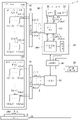
본 발명의 제1의 실시형태에 따른 측정 시스템(1)을 도 1에 나타낸다. 측정 시스템(1)은, 반도체 기판(2)의 주면에 형성된 광 반도체 소자(200)의 특성을 측정한다. 측정 시스템(1)은, 광 반도체 소자(200)에 대향해서 배치된 프로브 유닛 (10)과, 광 반도체 소자(200)를 구동하는 구동장치(20)와, 광 반도체 소자(200)에서의 출사광을 처리하는 처리장치(30)를 구비한다. 측정 시스템(1)은, 반도체 기판(2)을 스테이지(55)에 탑재한 상태에서 광 반도체 소자(200)의 특성을 측정한다.A
측정 시스템(1)은, 제어 장치(40) 및 프로버 컨트롤러(prober controller)(50)를 더 포함한다. 프로버 컨트롤러(50)는, 프로브 유닛(10)이나 스테이지(55)의 위치를 조정한다. 제어 장치(40)는, 측정 시스템(1)의 동작 전체를 제어한다. 예를 들면, 제어 장치(40)로부터의 제어 신호에 응답해서, 구동 장치(20), 처리 장치(30), 프로버 컨트롤러(50)가 동작한다. 또한, 제어장치(40)는, 처리장치(30)에 의해 얻어진 광 반도체 소자(200)로부터의 출사광의 데이터를 처리하고 광 반도체 소자(200)의 특성을 산출하는 기능도 갖는다. 제어 장치(40)로는, 예를 들어 개인용 컴퓨터(PC) 등을 사용해도 좋다.The
후술하는 바와 같이, 측정 시스템(1)에서는, 광 출력(IL) 특성, 순방향 전압 Vf, 역방향 전류 Ir 등의 광 전기 특성을, 복수의 광 반도체 소자(200)에 대해서 동시에 측정한다. 또한, 측정 시스템(1)에서는, 분광 특성에 대해 광 반도체 소자 (200)를 1개씩 측정한다. 이하에서 복수의 광 반도체 소자(200)에 대해 동시에 행하는 측정을 「패럴렐 측정(parallel measurement)」이라고도 칭한다. 또한, 광 반도체 소자(200)에 대하여 1개씩 차례로 행하는 측정을 「시리얼 측정(serial measurement)」이라고도 칭한다.As will be described later, in the
도 1에 나타내는 바와 같이, 프로브 유닛(10)은, 광 프로브(11)(1,1)~광 프로브(11)(m,n)을 갖는 광 프로브 어레이(110)를 포함한다. 이하에서는, 광 프로브(11)(1,1)~광 프로브(11)(m,n)를 「광 프로브(11)」이라고도 칭한다. 광 프로브(11)의 선단은, 광 반도체 소자(200)의 광 신호 단자와 광학적으로 접속한다. 측정 시스템(1)에서는, 광 프로브(11)가 광 반도체 소자(200)에서의 출사광을 수광하는 광 접속 장치로서 사용된다.As shown in FIG. 1 , the
예를 들면, 광 프로브 어레이(110)는, 반도체 기판(2)의 주면의 면 법선 방향에서 보아서(이하,「평면시(planar view)라 함), m×n개의 광 프로브(11)의 선단을 m행 n열의 매트릭스 형태로 배치한 구성을 가진다. 이 경우, n심(core)의 다심 프로브를 m열 배치해서 광 프로브 어레이(110)를 구성해도 좋다. For example, in the
또한, 프로브 유닛(10)은, 전기 프로브 어레이(120)를 구비한다. 전기 프로브 어레이(120)는, 광 프로브(11)(1,1)~광 프로브(11)(m,n)에 각각 대응해서 배치 된 전기 프로브(12)(1,1)~전기 프로브(12)(m,n)를 갖는다. 이하에서, 전기 프로브 (12)(1,1)~전기 프로브(12)(m,n)를 「전기 프로브(12)」라고도 칭한다. 전기 프로브(12)의 선단은, 광 반도체 소자(200)의 전기 신호 단자와 전기적으로 접속한다.In addition, the
반도체 기판(2)에 형성된 광 반도체 소자(200)의 배치와, 광 프로브(11) 및 전기 프로브(12)의 배치는 대응한다. 예를 들면, m×n개의 광 프로브(11)의 선단을 m행 n열의 매트릭스 형태로 배치한 경우, m×n개의 전기 프로브(12)의 선단이 m행 n열의 매트릭스 형태로 배치되도록 전기 프로브 어레이(120)를 구성한다.The arrangement of the
그리고, 광 반도체 소자(200)의 배치 피치와, 광 프로브(11) 및 전기 프로브 (12)의 배치 피치를 일치시킨다. 그에 따라, 광 프로브 어레이(110)와 반도체 기판 (2)의 위치 맞춤에 의해 m×n개의 광 반도체 소자(200)와, m×n개의 광 프로브(11) 및 m×n개의 전기 프로브(12)가 동시에 위치 맞춤된다. 동일한 광 반도체 소자(200)에 접속하는 광 프로브(11)와 전기 프로브(12) 세트를, 아래에서 「프로브 세트」라고 칭한다.And the arrangement pitch of the
도 1에 나타내는 측정 시스템(1)에서는, 1개의 광 반도체 소자(200)에 대응하는 하나의 프로브 세트가, 1개의 광 프로브(11)와 1개의 전기 프로브(12)에 의해 구성되어 있다. 그러나, 하나의 프로브 세트를 구성하는 광 프로브(11)나 전기 프로브(12)의 갯수는 복수이어도 좋다. 예를 들면, 1개의 광 반도체 소자(200)에 대해서 광 반도체 소자(200)에 구동 전류를 공급하는 전기 프로브(12)와. 광 반도체 소자(200)의 접지 단자에 접속하는 GND용의 전기 프로브(12)를 사용해도 좋다. 이와 같이, 1개의 광 반도체 소자(200)에 대해서 배치하는 광 프로브(11)나 전기 프로브(12)의 개수는, 광 반도체 소자(200)의 사양 등에 따라서 임의로 설정해도 좋다. In the
측정 시스템(1)에 의한 광 반도체 소자(200)의 측정에서는, 먼저 광 반도체 소자(200)와 프로브 유닛(10)의 위치 맞춤을 수행한다. 광 반도체 소자(200)와 프로브 유닛(10)의 위치 맞춤에 의해 광 반도체 소자(200)의 광 신호 단자가 광 프로브(11)와 광학적으로 접속한다. 동시에, 광 반도체 소자(200)의 전기 신호 단자가 전기 프로브(12)와 전기적으로 접속한다.In the measurement of the
광 반도체 소자(200)와 프로브 유닛(10)을 위치 맞춤한 상태에서, 구동 장치(20)는, 전기 프로브(12)(1,1)~전기 프로브(12)(m,n)에, 구동 전류 I(1,1)~구동 전류I(m,n)를 공급한다. 이하에 있어서, 구동 전류I(1,1)~구동 전류I(m, n)를 「구동 전류 I」라고도 칭한다. 구동 장치(20)에서, 구동 전류 I는 전기 배선 E를 전파한다. 전기 배선 E는, 구동 전류 I가 각각 전파하는 복수의 전기 배선의 세트이다. 프로브 유닛(10)과 구동 장치(20) 사이에 배치된 제1 접속반(first connection board)(61)을 통해서 구동장치(20)로부터 광 반도체 소자(200)에 구동 전류 I가 공급된다.In a state in which the
예를 들면, 구동 장치(20)는, 도 2에 나타내는 바와 같이, m×n개의 전기 프로브(12)에 각각 접속하는 m×n개의 드라이버(21)(1,1)~드라이버(21)(m,n)를 갖는다. 드라이버(21)(1,1)~드라이버(21)(m,n)은, 전기 프로브(12)(1,1)~전기 프로브(12)(m,n)와 1대 1로 대응한다. 이하에서는, 드라이버(21)(1,1)~드라이버(21)(m,n)를 「드라이버(21)」이라고도 칭한다. 구동 장치(20)는, 전기 프로브(12)를 통해서 드라이버(21)에서 광 반도체 소자(200) 각각에 구동 전류 I를 공급한다.For example, as shown in Fig. 2, the
측정 시스템(1)에서는, 제어 장치(40)가, 구동 전류 I를 광 반도체 소자(200)에 공급하기 위한 제어 신호를 구동 장치(20)로 출력한다. 제어 신호를 수신한 구동 장치(20)의 드라이버(21)는, 각각의 드라이버(21)가 접속하는 광 반도체 소자(200)에 구동 전류 I를 공급한다. 예를 들면, 제어 장치(40)는 시리얼 제어 신호를 출력하고, 이 시리얼 제어 신호가 패럴렐 제어 신호로 변환되어서 드라이버(21)에 각각 송신된다.In the
전기 프로브(12)에서 공급된 구동 전류 I에 의해, 광 반도체 소자(200)가 통전한다. 그리고, 통전한 광 반도체 소자(200)로부터의 출사광을, 구동 전류 I를 공급한 전기 프로브(12)과 함께 프로브 세트를 구성하는 광 프로브(11)가 수광한다.The
패럴렐 측정에서는, m×n개의 광 반도체 소자(200)에 대해서 동시에 통전한다. 이때, m×n개의 광 반도체 소자(200)로부터의 출사광을, m×n개의 광 프로브 (11)가 각각 수광한다. 광 프로브(11)(1,1)~광 프로브(11)(m,n)가 수광하는 출사 광을, 출사광 L(1,1)~출사광 L(m,n)로 한다. 출사광 L(1,1)~출사광 L(m,n)을 「출사광 L」이라고도 칭한다. 출사광 L은, 제2 접속반(second connection board)(62) 및 광 배선 F를 경유해서, 처리 장치(30)의 광 분기 장치(310)로 입력한다. 광 배선 F는, 출사광 L이 각각 전파하는 복수의 광 배선 세트이다. In parallel measurement, m x n
광 분기 장치(310)는, 광 프로브(11)(1,1)~광 프로브(11)(m,n)가 수광한 출사광 L(1,1)~출사광 L(m, n) 각각을, 제1 분기광 L1(1,1)~제1 분기광 L1(m,n)과, 제2 분기광 L2(1,1)~제2 분기광 L2(m,n)로 분기한다. 제1 분기광 L1(1,1)~제1 분기광 L1(m,n)을 「제1 분기광 L1」라고도 칭한다. 제2 분기광 L2(1,1)~제2 분기광 L2(m,n)을 「제2 분기광 L2」라고도 칭한다. 광 분기 장치(310)에서 광 배선 F1을 전파해서, 제1 분기광 L1은 합류기(32)에 입력한다. 광 배선 F1은, 제1 분기광 L1이 각각 전파하는 복수의 광 배선 세트이다. 또한, 광 분기 장치(310)에서 광 배선 F2를 전파하고, 제2 분기광 L2는 광전 변환 장치(340)에 입력한다. 광 배선 F2는, 제2 분기광 L2가 각각 전파하는 복수의 광 배선 세트이다. The optical branching
예를 들면, 광 분기 장치(310)는, 도 3에 나타내는 바와 같이, m×n개의 광 커플러(31)(1,1)~광 커플러(31)(m,n)를 갖는다. 광 커플러(31)(1,1)~광 커플러(31) (m,n)은, 광 프로브(11)(1,1)~광 프로브(11)(m,n)와 1대 1로 대응한다. 광 커플러 (31)(1,1)~광 커플러(31)(m,n)는, 광 프로브(11)(1,1)~광 프로브(11)(m,n)가 수광 한 출사광 L 각각을 제1 분기광 L1와 제2 분기광 L2로 분할한다. 이하에서는, 광 커플러(31)(1,1)~광 커플러(31)(m,n)를 「광 커플러(31)」라고도 칭한다.For example, as shown in Fig. 3, the optical branching
제2 접속반(62)은, 예를 들면 m×n개의 커넥터를 갖는 다심의 어댑터를 갖는다. 제2 접속반(62)의 커넥터를 통해서 광 프로브(11)와 광 커플러(31)가 광학적으로 접속한다. 제2 접속반(62)은, 예를 들면, 다련(多連) 어레이 타입이나 다심(多芯) 커넥터 타입의 구성이 가능하다.The second connecting
이하에 설명하는 바와 같이, 제1 분기광 L1은 시리얼 측정에 사용된다. 또한 제2 분기광 L2는 패럴렐 측정에 사용된다. 예를 들면, 제1 분기광 L1은 출사광 L의 10%정도이며, 제2 분기광 L2는 출사광 L의 90%정도이다.As described below, the first branch light L1 is used for serial measurement. Also, the second branch light L2 is used for parallel measurement. For example, the first branched light L1 is about 10% of the emitted light L, and the second branched light L2 is about 90% of the emitted light L.
제1 분기광 L1은, 광 반도체 소자(200)의 출사광 L에 대한 분광 특성의 측정 등에 사용한다. 구체적으로는 m×n개의 광 프로브(11)가 수광한 m×n개의 출사광 L의 제1 분기광 L1은, m×n개의 입력 단자와 1개의 출력 단자를 갖는 합류기(32)의, 입력 단자에 각각 입력한다. 시리얼 측정에서는, 후술하는 바와 같이, 합류기(32)에 차례로 입력한 제1 분기광 L1이, 합류기(32)의 출력 단자에서 분광 모듈(33)에 출력된다. 분광 모듈(33)은, 입력된 제1 분기광 L1을 분광한다.The first branched light L1 is used for, for example, measurement of a spectral characteristic of the
합류기(32)에는, 예를 들면, Y분기로 구성된 광 도파로 타입의 구성 등을 적합하게 사용할 수 있다. 이 구성의 합류기(32)는, 형상이 소형이며, 합류기로서 사용하는 경우에 손실이 적어 취급하기 쉽다. 혹은, 1입력 2분기 출력의 융착 연신형 광 커플러를 다단으로 융착 접속해서 합류기(32)를 구성해도 좋다.For the merging
분광 모듈(33)에 의한 제1 분기광 L1의 분광에 의해 출사광 L의 분광 특성을 측정할 때에, 제어 장치(40)는, 구동하는 광 반도체 소자(200)를 하나씩 선택한다. 예를 들면, 제어 장치(40)는 광 반도체 소자(200)에 구동 전류 I를 공급하는 드라이버(21)를 차례로 선택한다. 선택된 드라이버(21)가 구동하는 광 반도체 소자(200)로부터의 출사광 L의 제1 분기광 L1이, 합류기(32)에서 출력한다. 합류기(32)에서 출력된 제1 분기광 L1은, 분광 모듈(33)에 입력한다. 분광 모듈(33)은 제1 분기광 L1을 분광하고, 분광한 데이터를 제어 장치(40)로 송신한다. 이에 따라, 선택된 광 반도체 소자(200)의 분광 특성이 측정된다. 제어 장치(40)가 광 반도체 소자(200)를 하나씩 선택함에 따라, m×n개의 광 반도체 소자(200)의 분광 특성이 차례로 측정된다.When the spectral characteristics of the emitted light L are measured by the spectroscopy of the first branched light L1 by the
상기와 같이, 분광 모듈(33)에 의해, 복수의 광 프로브(11)가 각각 수광한 출사광 L의 제1 분기광 L1이 하나씩 분광된다. 이처럼, 분광 모듈(33)에 의한 분광 특성의 측정은, 시리얼 측정이다. 분광 모듈(33)에 의해 얻어지는 분광 특성은, 제어 장치(40)에 접속하는 기억 장치에, 광 반도체 소자(200)에 대응지어서 보존된다.As described above, the first branched light L1 of the emitted light L received by the plurality of
출사광 L에서 분기된 제2 분기광 L2은, 광 신호/전기 신호 변환(OE변환)되고, 광 반도체 소자(200)의 출사광 L에 대한 광 출력(IL) 특성, 순방향 전압 Vf, 역방향 전류 Ir 등의 광전기 특성의 측정에 사용된다. 구체적으로는, m×n개의 광 프로브(11)에서 출사된 m×n개의 출사광 L의 제2 분기광 L2는, 처리 장치(30)의 광전 변환 장치(340)에 입력한다. 광전 변환 장치(340)는, m×n개의 제2 분기광 L2 각각을 OE 변환한다.The second branched light L2 branched from the emitted light L is converted into an optical signal/electrical signal (OE conversion), and the optical output (IL) characteristic of the
광전 변환 장치(340)는, 광 프로브(11)와 1대 1로 대응하는 복수의 광전 변환기(OE변환기)를 갖는다. OE 변환기 각각에, 광 프로브(11)가 수광한 출사광 L의 제2 분기광 L2가 1개씩 입력한다. 예를 들면, 광전 변환 장치(340)는, 도 4에 나타내는 바와 같이, m×n개의 광 프로브(11)와 1대 1로 광학적으로 접속하는 m×n개의 OE 변환기(34)(1,1)~OE 변환기(34)(m,n)를 갖는다. 이하에서는, OE 변환기(34)(1,1)~OE 변환기(34)(m,n)를 「OE 변환기(34)」라고도 칭한다. 광 프로브(11)와 OE 변환기(34)는, 광 커플러(31)를 통해서 광학적으로 접속한다. 광 프로브(11)가 각각 수광한 출사광 L 중 적어도 일부가 제2 분기광 L2로서 OE 변환기(34)에 입력한다. OE 변환기(34)는, 제2 분기광 L2를 전기 신호로 변환한다.The
광전 변환 장치(340)에 의해 제2 분기광 L2에서 전기 신호로 변환된 전기 신호는, 변환기(35)에 의해 아날로그/디지털(AD) 변환된다. 그리고 또한, 변환기(35)는, 디지털 변환된 m×n개의 전기 신호에 대해서 패럴렐/시리얼 변환한다. 시리얼 변환된 데이터는 제어 장치(40)로 송신되고, 광 반도체 소자(200)의 특성이 취득, 순차적으로 격납된다. 예를 들면, 제어 장치(40)가 구동 전류 I와 제2 분기광 L2의 데이터를 처리함으로써, 광 출력(IL) 특성, 순방향 전압 Vf, 역방향 전류 Ir 등의 광전기 특성이, 광 반도체 소자(200) 대해서 측정된다.The electrical signal converted into the electrical signal in the second branch light L2 by the
상기와 같이, 광전변환장치(340)를 이용한 측정은, m×n개의 광 반도체 소자 (200)를 동시에 통전하고, m×n개의 광 반도체 소자(200)에서의 출사광 L을 처리하는 패럴렐 측정이다. 복수의 OE 변환기(34)가, 복수의 광 반도체 소자(200)에서의 출사광 L을 동시에 처리한다. 패럴렐 측정에 의해 얻어진 특성은,제어 장치(40)에 접속하는 기억장치에, 광 반도체 소자(200)에 대응지어서 보존된다. As described above, the measurement using the
도 5는, 측정 시스템(1)을 이용한 1개분의 광 반도체 소자(200)에 대한 측정계의 일부를 나타낸다. 광 반도체 소자(200)와 프로브 유닛(10)의 위치 맞춤에 의해, 전기 프로브(12)는 광 반도체 소자(200)의 전기 신호 단자(미도시)와 접속한다. 이때, 광 프로브(11)의 선단과 광 반도체 소자(200)의 광 신호 단자(미도시)의 작동 거리 WD는, 광 프로브(11)와 광 반도체 소자(200)의 광 신호 단자가 광학적으로 접속하는 거리로 설정된다. 또한, 전기 프로브(12)에는 탄성이 있기 때문에 전기 프로브(12)가 광 반도체 소자(200)와 접속한 상태인 채로 작동 거리 WD에 대해 수십 μm정도의 조정은 가능하다. 프로브 유닛(10)의 프로브 고정부(13)에 광 프로브(11)와 전기 프로브(12)가 지지되어서 광 프로브(11)와 전기 프로브(12)의 위치가 고정된다. 광 프로브(11)와 전기 프로브(12)는 별개의 프로브 고정부(13)에 의해 고정 지지해도 좋다. FIG. 5 shows a part of the measurement system for one
광 반도체 소자(200)와 프로브 유닛(10)의 위치 맞춤에서는, 예를 들면, 프로버 컨트롤러(50)의 제어에 의해, 반도체 기판(2)의 주면과 평행한 XY 평면 및 반도체 기판(2)의 주면에 수직인 Z방향에 대해 프로브 유닛(10)이 이동한다. 혹은, 프로버 컨트롤러(50)의 제어에 의해 XY 평면 및 Z방향에 대해, 반도체 기판(2)을 탑재한 상태에서 스테이지(55)를 이동한다. 또한, 스테이지(55)는 Z방향을 중심축으로서 회전 가능하다. 광 반도체 소자(200)에 대해서 광 프로브(11) 및 전기 프로브(12)를, 예를 들면 수 μm 단위로 위치 맞춤이 가능하다.In the alignment of the
광 반도체 소자(200)에서의 출사광 L이 입사하는 광 프로브(11)의 선단은, 예를 들면, 멀티모드 파이버 또는 싱글모드 파이버로 구성된다. 광 프로브(11)의 선단은, 구형상으로 성형 가공되어 있어도 좋다. 광 프로브(11)의 선단을 구형상으로 함으로써 광 프로브(11)의 선단의 개구수 NA의 조정, 작동거리 WD, 광 프로브(11)의 선단에서의 출사광 L의 반사 귀환광(return light)의 절감 등에 대응할 수 있다. 그 결과, 광 프로브(11)의 선단에 있어서 출사광 L을 안정적으로 수광할 수 있다.The tip of the
도 5에 도시한 상태에 있어서, 드라이버(21)가, 예를 들면 직류 전류 또는 수μ초~수십μ초의 펄스 전류의 구동 전류 I를 출력한다. 구동 전류 I는, 제1 접속반(61) 및 전기 프로브(12)를 통해서 광 반도체 소자(200)에 공급된다. 구동 전류 I가 공급된 광 반도체 소자(200)는, 출사광 L을 출사한다. 광 프로브(11)는, 광 반도체 소자(200)에서의 출사광 L을 수광한다. 광 프로브(11)를 전파한 출사광 L은, 제2 접속반(62)을 통해서 광 커플러(31)에 전파한다. 광 커플러(31)는, 출사광 L을 제1 분기광 L1과 제2 분기광 L2로 분기한다. 제1 분기광 L1은 합류기(32)를 통해서 분광 모듈(33)에 입력한다. 제2 분기광 L2는, OE 변환기(34)에 입력한다.In the state shown in Fig. 5, the
이상에서 설명한 바와 같이, 측정 시스템(1)은, m×n개의 광 프로브(11)에 각각 접속하는 m×n개의 OE 변환기(34)와, m×n개의 전기 프로브(12)에 각각 접속하는 m×n개의 드라이버(21)를 구비한다. 이에 따라, 측정 시스템(1)에 의하면, m×n개의 광 반도체 소자(200)를 동시에 측정하는 패럴렐 측정과, 광 반도체 소자(200)를 1개씩 측정하는 시리얼 측정이 가능하다.As described above, the
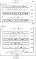
도 6을 참조해서, 측정 시스템(1)에 의해 m×n개의 광 반도체 소자(200)를 측정하는 방법의 예를 이하에 설명한다. 도 6은, 단계 S10에 나타내는 패럴렐 측정을 행한 후에, 단계 S20에 나타내는 시리얼 측정을 행하는 경우를 예시하고 있다.With reference to FIG. 6, the example of the method of measuring the mxn
우선, 단계 S10의 단계 S11에 있어서, 구동 장치(20)가 m×n개의 광 반도체 소자(200)를 동시에 구동한다. 단계 S12에 있어서, 광 프로브(11)가, 광 반도체 소자(200)로부터의 출사광 L을 수광한다. 그리고, 단계 S13에 있어서, 광 분기 장치(310)가 광 프로브(11)에 의해 수광한 m×n개의 출사광 L 각각을, 제1 분기광 L1와 제2 분기광 L2으로 분기한다.First, in step S11 of step S10, the driving
단계 S14에 있어서, 광전 변환 장치(340)가, m×n개의 제2 분기광 L2를 동시에 광전 변환한다. 광전 변환에 의해 제2 분기광 L2에서 변환된 전기 신호는, 변환기(35)를 통해서 제어 장치(40)에 송신된다. In step S14, the
단계 S15에 있어서, 제어 장치(40)는, 광 반도체 소자(200)에 공급된 구동 전류 I 및 제2 분기광 L2에서 얻은 전기 신호를 이용하여, m×n개의 광 반도체 소자(200)의 광 전기 특성을 취득한다. 예를 들면, 구동 전류 I와 제2 분기광 L2의 데이터를 이용해서, 광 반도체 소자(200)의 광 출력(IL) 특성, 순방향 전압 Vf, 역방향 전류 Ir이 취득된다.In step S15 , the
이어서, 단계 S20의 단계 S21에 있어서, 제어 장치(40)가 1개의 광 반도체 소자(200)를 선택한다. 단계 S22에 있어서, 구동 장치(20)가, 선택된 광 반도체 소자(200)에 구동 전류 I를 공급해서 광 반도체 소자(200)를 구동한다. 단계 S23에 있어서, 광 프로브(11)가, 구동한 광 반도체 소자(200)에서의 출사광 L을 수광한다. 그리고, 단계 S24에 있어서, 광 분기 장치(310)가, 광 프로브(11)가 수광한 출사광 L을 제1 분기광 L1과 제2 분기광 L2로 분기한다.Next, in step S21 of step S20 , the
단계 S25에 있어서, 합류기(32)를 통해서 분광 모듈(33)에 입력한 제1 분기 광 L1을, 분광 모듈(33)이 분광한다. 분광 모듈(33)이 분광한 파장 특성 데이터는 제어 장치(40)에 송신된다. 단계 S26에 있어서, 제어 장치(40)는, 분광 모듈(33)이 분광한 파장 특성 데이터를 이용하여, 선택한 광 반도체 소자(200)의 분광 특성을 취득한다. In step S25 , the first branched light L1 input to the
단계 S27에 있어서, 제어 장치(40)는, m×n개의 광 반도체 소자(200)를 모두 선택했는지 여부를 판정한다. 선택하지 않은 광 반도체 소자(200)가 있는 경우는, 처리는 단계 S21로 돌아온다. 모든 광 반도체 소자(200)를 선택하면, 처리를 종료한다.In step S27, the
광 반도체 소자(200)의 분광 특성의 측정은, m×n번 반복된다. 따라서, 분광 모듈(33)에 의한 측정 시간이 짧을수록 시리얼 측정에 요하는 시간을 단축할 수있다. 따라서, 분광 모듈(33)은 적절한 파장 분해 능력을 가지고, 수광 적산 시간이 밀리초 단위로 짧아 측정 데이터의 전송 레이트가 빠른 것이 측정 시간 단축에 바람직하다.The measurement of the spectral characteristics of the
상기에서는, 패럴렐 측정에 의해 m×n개의 광 반도체 소자(200)에 대해서 동시에 광 전기 특성을 측정한 후, 시리얼 측정에 의해 m×n개의 광 반도체 소자(200)의 분광 특성을 하나씩 측정하는 예를 설명하였다. 그러나, 측정 시스템(1)에 의한 측정에서는, 패럴렐 측정과 시리얼 측정의 순서는 임의로 설정 가능하다. 예를 들면, 시리얼 측정 후에 패럴렐 측정을 실시해도 좋다. 또한, 패럴렐 측정 도중에서 시리얼 측정을 행해도 좋다. 즉, 패럴렐 측정에 의해 측정되는 특성과 시리얼 측정에 의해 측정되는 특성의 측정 순서는, 임의로 설정 가능하다.In the above, an example of measuring the spectral characteristics of m×n
반도체 기판(2)에 형성된 모든 광 반도체 소자(200)를 측정하기 위해서는, m×n개의 광 반도체 소자(200)의 측정이 종료할 때마다 반도체 기판(2) 또는 프로브 유닛(10)을 이동시켜, 미측정의 광 반도체 소자(200)를 측정한다. 그리고, 반도체 기판(2)에 형성된 모든 광 반도체 소자(200)의 측정이 종료할 때까지 도 6을 참조해서 설명한 광 반도체 소자(200)의 측정을 반복한다.In order to measure all the
측정 시스템(1)에 의하면, m×n개의 광 반도체 소자(200)의 측정을 반복함으로써 반도체 기판(2)에 형성된 모든 광 반도체 소자(200)의 측정을 효율적으로 실행할 수 있다. 이하에서, 측정 시스템(1)에 의해 동시에 측정 가능한 광 반도체 소자(200)의 개수를, 측정 시스템(1)의 「채널 수」라고도 칭한다. 도 1에 나타내는측정 시스템(1)의 채널 수는, m×n이다.According to the
반도체 기판(2)에 형성된 광 반도체 소자 (200)의 총수가 Nw개인 경우, m×n 개의 광 반도체 소자(200)의 측정을 반복하는 횟수는, 최소로 대략 Nw/채널이다. 측정 시스템(1)에 의한 측정에서는 광 반도체 소자(200)의 1개씩에 대해 광 프로브 (11)와 전기 프로브(12)의 위치 맞춤을 하는 측정에 비해서 반도체 기판(2)에 형성된 모든 광 반도체 소자(200)를 측정하는 것에 요하는 시간을 대폭 단축할 수 있다.When the total number of the
또한, m×n개의 광 반도체 소자(200)에 대응하는 m×n개의 분광 모듈(33)을 처리 장치(30)에 준비하는 구성도 생각할 수 있다. 그러나, 그 구성은, 비용이나 실장 공간의 증대가 커서 비효율적이다. 도 1에 나타내는 측정 시스템(1)에 의하면, 간단한 회로 구성과 효율적인 동작에 의해, 다채널 측정에 의한 측정 시간의 단축을 실현할 수 있다. Further, a configuration in which m×n
이하에, 측정 시스템(1)에 의한 광 반도체 소자(200)의 측정 시간에 대해 설명한다. 여기서, 프로브 유닛(10)과 반도체 기판(2)의 위치 맞춤 시간을 tp, 패럴렐 측정 시간에 요하는 시간을 tm, m×n개의 광 반도체 소자(200)의 시리얼 측정에 요하는 시간을 tb로 한다. 이 경우, 측정 시스템(1)에 의해 m×n개의 광 반도체 소자(200)의 측정에 요하는 총 측정 시간 Tk1는, 아래의 식(1)로 나타내어진다:Hereinafter, the measurement time of the
Tk1 = tp + tm + tb…(1)Tk1 = tp + tm + tb… (One)
시리얼 측정에서의 1개의 광 반도체 소자(200)의 측정 시간을 ts로 하면, tb= ts×(m×n)이다.Assuming that the measurement time of one
또한, 여러 측정 항목에 관해서 측정하는 패럴렐 측정에서는, 광 반도체 소자(200)를 방열시키기 위해, 광 반도체 소자(200)로의 구동 전류 I의 공급을 정지하는 시간(이하, 「슬립 시간(sleep time) tr」이라고 칭한다)을, 측정항목 사이에서 설치해도 좋다. 이 경우, 패럴렐 측정에 있어서 구동 전류 I를 광 반도체 소자 (200)에 공급하는 시간을 tl으로 해서, tm=tl + tr이다.Note that, in parallel measurement for measuring various measurement items, the time for stopping the supply of the driving current I to the
도 7a 및 도 7b에, 채널 수가 64인 측정 시스템(1)을 이용한 광 반도체 소자 (200)의 측정 시간의 예를 나타낸다. 도 7a에 나타내는 시간 t1은, 구동전류 I=4mA에서의 순방향 전압 Vf의 측정 시간이다. 시간 t2는, 구동 전류 I=4mA에서의 광출력(IL) 특성의 측정 시간이다. 시간 t3는, 구동 전류 I=9mA에서의 순방향 전압 Vf의 측정 시간이다. 시간 t4는, 구동전류 I=9mA에서의 광 출력(IL) 특성의 측정 시간이다. 시간 t5는, 역방향 전류 Ir의 측정 시간이다. 도 7a에 나타내는 바와 같이 순방향 전압 Vf와 광 출력(IL)의 특성의 측정 후에, 각각 슬립 시간을 마련하고 있다. 슬립 시간 tr의 설정은, 특히 광 반도체 소자(200)가 통전에 의한 국부적인 가열에 의해 열화하기 쉬운 경우, 효과적이다.7A and 7B, an example of the measurement time of the
구동 전류 I=4mA에서의 측정 데이터와 구동 전류 I=9mA에서의 측정 데이터를 이용하여, 광 반도체 소자(200)의 임계치 전류(threshold current)나 기울기 효율(slope efficiency)을 산출할 수 있다.A threshold current or slope efficiency of the
예를 들면, 도 7b에 나타내는 바와 같이, 순방향 전압 Vf의 측정에 요하는 시간 t1 및 시간 t3는 10m초, 광 출력(IL) 특성의 측정에 요하는 시간 t2 및 시간 t2는 13m초이다. 또한, 시리얼 측정에서의 1개의 광 반도체 소자(200)의 측정 시간 ts는 2m초이며, tb=ts×64=128초이다. 슬립 시간은 각각 100m초이며, 총 슬립 시간 tr은 400m초이다. 따라서, 도 7a 및 도 7b에 나타내는 측정에서는, 64개의 광 반도체 소자(200)의 측정에 요하는 총 측정 시간은 574m초이다.For example, as shown in Fig. 7B, the time t1 and time t3 required for the measurement of the forward voltage Vf are 10 m seconds, and the time t2 and time t2 required for the measurement of the light output (IL) characteristic are 13 m seconds. In addition, the measurement time ts of one
(제2의 실시형태)(Second embodiment)
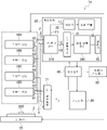
본 발명의 제2의 실시형태에 따른 측정 시스템(1a)은, 도 8에 나타내는 바와 복수의 프로브 유닛(10)을 갖는다. 측정 시스템(1a)에서는, 프로브 유닛(10A)~프로브 유닛(10D) 중 어느 것과 구동 장치(20) 및 광전 변환 장치(340)를 접속해서 프로브 유닛(10)마다 광 반도체 소자(200)의 출사광 L을 처리한다. 측정 시스템(1a)은, 구동 장치(20)가 접속하는 프로브 유닛(10)을 절환(switch)하는 제1 절환 회로(71)와, 광전 변환 장치(340)가 접속하는 프로브 유닛(10)을 절환하는 제2 절환 회로(72)를 구비한다.A
또한, 도 8에서는, 측정 시스템(1a)이 4개의 프로브 유닛(10)을 갖는 구성을 나타냈지만, 측정 시스템(1a)이 구비하는 프로브 유닛(10)의 개수는 임의이다. 이하에 있어서, 측정 시스템(1a)이 가지는 프로브 유닛(10)의 수를 U로 나타낸다.In addition, although the structure which the
프로브 유닛(10)의 개수를 늘림으로써 측정에 사용하는 광학 프로브(11)와 전기 프로브(12)의 개수를 증가시킬 수 있다. 측정 시스템(1a)에 따르면, 프로브 유닛(10)과 반도체 기판(2)의 한번의 위치 맞춤에 의해, 광 프로브(11) 및 전기 프로브(12)와 위치 맞춤된 광 반도체 소자(200)의 개수가 증가하고, 위치 맞춤의 횟수를 줄일 수 있다.By increasing the number of
도 8에 나타내는 측정 시스템(1a)의 OE 변환기(34)나 드라이버(21)의 수는, 도 1의 측정 시스템(1)과 같다. 따라서, 측정 비용이나 실장 공간의 증대를 억제할 수 있다. 도 8에 나타내는 측정 시스템(1a)에서는, 프로브 유닛(10A)~프로브 유닛(10D) 중 어느 것의 전기 프로브(12)를 구동 장치(20)와 선택적으로 접속한다. 그리고, 선택한 전기 프로브(12)와 프로브 세트를 구성하는 광 프로브(11)를, 광전 변환 장치(340)에 접속한다. The number of
프로브 유닛(10A)~프로브 유닛(10D)과 구동 장치(20) 사이에 배치된 제1 절환 회로(71)는, 예를 들면 m×n개의 아날로그 스위치를 갖는 구성이어도 좋다. 아날로그 스위치의 입력 단자는 구동 장치(20)의 드라이버(21)와 접속한다. 아날로그 스위치의 4개의 출력 단자는, 프로브 유닛(10A)~프로브 유닛(10D)의 전기 프로브 (12)에 접속한다. 그리고, m×n개의 아날로그 스위치는, m×n개의 드라이버(21)와 m×n개의 전기 프로브(12)를 1대 1로 접속한다. 아날로그 스위치의 절환에 의해, 프로브 유닛(10A)~프로브 유닛(10D) 중 어느 것의 전기 프로브(12)와 드라이버(21)가 접속한다. The
측정 시스템(1a)의 광 분기 장치(310)는 프로브 유닛(10A)~프로브 유닛(10D)에 포함된 모든 광 프로브(11)와 1대 1로 대응하는, m×n×U개의 광 커플러(31)를 가진다. 광 분기 장치(310)와 광전 변환 장치(340) 사이에 배치된 제2 절환 회로(72)는, 프로브 유닛(10)마다 광 프로브(11)와 OE 변환기(34)를 광 커플러(31)를 통해서 광학적으로 접속한다.The optical branching
제2 절환 회로(72)는, 예를 들면 m×n개의 광 스위치를 갖는 구성이어도 좋다. 제2 절환 회로(72)의 광 스위치의 절환에 의해 프로브 유닛(10A)~프로브 유닛(10D) 중 어느 하나의 광 프로브(11)가, 광 커플러(31)를 통해서 OE 변환기(34)와 접속한다. 광 스위치의 4개의 입력 단자는, 프로브 유닛(10A)~프로브 유닛(10D) 중 어느 것에 접속하는 4개의 광 커플러(31)에 접속하고, 광 스위치의 출력 단자는 OE 변환기(34) 중 하나에 접속한다. 그리고, 광 스위치에 의해 광 커플러(31)를 통한 프로브 유닛(10)과 광전 변환 장치(340)와의 접속이 바뀐다. 이와 같이, m×n개의 광 스위치는, 광 커플러(31)를 통해서 m×n개의 광 프로브(11)와 m×n개의 OE 변환기(34)를 1대 1로 접속한다.The
제1 절환 회로(71)나 제2 절환 회로(72)에서의 절환 동작은, 제어 장치(40)에 의해 제어된다. 그리고, 구동 장치(20)나 광전 변환 장치(340)와 접속하는 프로브 유닛(10)을 절환하면서 패럴렐 측정이 이루어진다. 시리얼 측정에서는, m×n×U개의 광 커플러(31)에서의 제1 분기광 L1이, m×n×U개의 입력 단자를 갖는 합류 기(32)에 입력하고, 합류기(32)의 출력 단자에서 제1 분기광 L1이 순서대로 출력된다. 그리고, 합류기(32)에서 출력되는 제1 분기광 L1을, 분광 모듈(33)이 분광한다.The switching operation in the
예를 들면, 프로브 유닛(10)의 수가 U개인 경우, 제2 절환 회로(72)에, U×1(U입력, 1출력)의 광 스위치를 m×n개 사용한다. 또한, 제1 절환 회로(71)에, U×1의 아날로그 스위치를 m×n개 사용하거나, 혹은 동등한 기능의 스위칭 소자를 사용해도 좋다. 따라서 m×n×U심의 광 프로브 어레이(110) 및 전기 프로브 어레이(120)를 실현할 수 있다. 광 스위치나 아날로그 스위치의 절환 횟수는, (U-1)회이다.For example, when the number of
U개의 프로브 유닛(10)을 갖는 측정 시스템에 의한 측정 시간 Tk1는, 이하의 식(2)로 표현된다:A measurement time Tk1 by a measurement system having
Tk1 = N×{tp+U×((tm+(m×n)×ts)+(U-1)×tsw)}…(2)Tk1 = N×{tp+U×((tm+(m×n)×ts)+(U-1)×tsw)}… (2)
식(2)에서, N은 반도체 기판(2)에 형성된 광 반도체 소자(200)의 개수가 Nw인 경우의 측정의 반복 횟수이다. 반복 횟수 N은, Nw/(U×(m×n))로 나타내어진다. 또한, 식(2)에서 tp는 1회의 위치 맞춤 시간, tm은 패럴렐 측정에 요하는 시간, ts는 시리얼 측정에 요하는 시간이다. tsw는, 광 스위치의 절환 시간이다.In Equation (2), N is the number of repetitions of the measurement when the number of
상기에서는, m×n×U개의 광 커플러(31)를 갖는 광 분기 장치(310)를 사용하는 예를 보여주었다. 그러나, m×n개의 광 커플러(31)를 갖는 U개의 광 분기 장치 (310)를 사용하고, 광 스위치에 의해 광 분기 장치(310)와 접속하는 프로브 유닛 (10)을 절환해도 좋다. 또한, 상기에서는 합류기(32)가 m×n×U개의 입력 단자를 갖는 예를 나타내었다. 그러나, m×n개의 입력 단자를 갖는 U개의 합류기(32)를 사용하여 광 분기 장치(310)와 접속하는 합류기(32)를 광 스위치에 의해 절환해도 좋다. In the above, an example of using the optical branching
측정 시스템(1a)에 의한 광 반도체 소자(200)의 측정에서는, 반도체 기판(2)에 형성된 모든 광 반도체 소자(200)를 측정할 때까지 m×n×U개의 광 반도체 소자 (200)의 측정이 종료할 때마다 반도체 기판(2) 또는 프로브 유닛(10)을 이동시킨다. 그리고, 새롭게 프로브 유닛(10)과 위치 맞춤한 광 반도체 소자(200)에 대해서 도 6을 참조해서 설명한 측정을 실행한다.In the measurement of the optical-
이상에 설명한 바와 같이, 제2의 실시형태에 따른 측정 시스템(1a)에서는, 광 프로브 어레이(110) 및 전기 프로브 어레이(120)를 갖는 프로브 유닛(10)을 U개(U≥2) 사용한다. 따라서, 측정 시스템(1a)에 따르면, 광 프로브(11) 및 전기 프로브(12)의 갯수를 도 1의 측정 시스템(1)의 U배로 늘리고, 또 도 1의 측정 시스템(1)의 구동 장치(20)나 광전 변환 장치(340)를 사용할 수 있다. 따라서, 측정 시스템의 확장성이 용이하다. 그리고 또한, 측정 시스템(1a)에 의하면, 광 반도체 소자(200)와 프로브 유닛(10)의 위치 맞춤 횟수가 감소하고, 측정 시간을 단축할 수 있다. 다른 것은 제1의 실시형태와 실질적으로 동일하고, 중복된 설명을 생략한다. 이하에서는, 프로브 유닛(10)을 갖는 측정 시스템(1) 및 측정 시스템(1a)을 총칭해서, 「측정 시스템(1)」이라고도 칭한다.As described above, in the
이하에, 측정 시스템(1)과, 도 9에 나타내는 비교 예의 측정 시스템(이하에 있어서, 단순히 「비교 예의 측정 시스템」이라고 한다)에 대하여 측정 시간을 비교한다.Below, the measurement time is compared with respect to the
비교 예의 측정 시스템은, 반도체 기판(2)에 형성된 광 반도체 소자(200)를, 전기 프로브(12)를 통해서 공급되는 구동 전류에 의해 구동한다. 광 반도체 소자(200)에서의 출사광 L은, 적분구(積分球)(300)에 의해 수광한다. 그리고, 출사광 L의 특성을, OE 변환기(34) 등의 측정 기기로 측정한다.The measurement system of the comparative example drives the
적분구(300)의 하부에 개구홀이 형성되고, 개구홀에서 광 반도체 소자(200)로부터의 출사광 L이 적분구(300)의 내부에 입사한다. 출사광 L은, 구상(球狀)의 적분구(300)의 내벽면에서 반복하여 반사해서 입사 강도가 평균화 된다. 적분구(300)의 내벽면에 포토디덱터(photodetector) 등의 OE 변환기를 설치함으로써 내벽면의 소정의 면적분의 입사 강도를 측정할 수 있다. 그리고, 적분구(300)의 내벽면의 면적분의 입사 강도를 곱함으로써 출사광 L의 강도를 산출할 수 있다. 출사광 L이 OE 변환기에 직접 조사하지 않도록 개구홀과 OE 변환기(34) 사이에 차광판(301)을 설치해도 좋다. 출사광 L의 분광 특성에 관해서는 적분구(300)의 내벽면에 설치한 파이버 콜리메이터(fiber collimator)(302)에 입사한 출사광 L을, 분광 모듈(33)에 입력해서 측정한다.An opening hole is formed in the lower portion of the integrating
비교 예의 측정 시스템에서는, 위치를 고정한 적분구(300)의 내부에 출사광 L이 동시에 입사하는 광 반도체 소자(200)가 m×n개의 경우, 반도체 기판(2)에 형성된 모든 광 반도체 소자(200)의 측정에 요하는 측정 시간 Tk2는, 이하의 식(3)으로 나타내어진다:In the measurement system of the comparative example, when there are m x n
Tk2= N×(tp+(m×n)×(tm+ts))…(3)Tk2=N×(tp+(m×n)×(tm+ts))… (3)
식(3)에서, N은, m×n개의 광 반도체 소자(200)의 측정의 반복 횟수이다. 또한 1회의 측정에서의 위치 맞춤 시간이 tp, 광전기 특성의 측정에 요하는 시간이 tm, 분광 특성의 측정에 요하는 시간이 ts이다. m×n은, 적분구(300)의 위치를 고정한 경우에 출사광 L을 수광할 수 있는 광 반도체 소자(200)의 개수이며, 측정 시스템(1)의 채널 수에 상당한다. 또한, 비교 예의 측정 시스템에서는, OE 변환기(34)에 의한 광 전기 특성의 측정과 분광 모듈(33)에 의한 분광 특성의 측정이 동시에 실행 가능하다. 이 경우, tm≥ts이면, 식(3)에서 ts=0이다. 다만, 비교 예의 측정 시스템에서는, 광 반도체 소자(200)는 하나씩 측정된다.In Formula (3), N is the number of repetitions of the measurement of the mxn optical-
한편, 측정 시스템(1)에 의한 총 측정 시간 Tk1은, 식(2)에 나타낸 바와 같다. 프로브 유닛(10)의 유닛 수 U는 1이며, 측정의 반복 횟수 N이 측정 시스템(1)과 비교 예의 측정 시스템에서 같은 경우, Tk2-Tk1=(m×n-1)×tm이다. 즉, 측정 시간을 비교하면, 비교 예의 측정 시스템보다도 측정 시스템(1) 쪽이, (m×n-1)×tm 만큼 측정 시간이 짧다.On the other hand, the total measurement time Tk1 by the
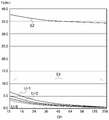
도 10에, 측정 시스템(1)과 비교 예의 측정 시스템의 측정 시간의 비교를 나타낸다. 도 10의 가로축은 채널 수 CH이며, 세로축은 반도체 기판(2)에 형성된 광 반도체 소자(200)의 총 측정 시간 Tk이다. 채널 수 CH는, m×n×U이다. 반도체 기판(2)에 형성된 광 반도체 소자(200)의 개수는 153,544개이다. 광전기 특성의 측정 요하는 시간이 tm=0.8초, 분광 특성의 측정에 요하는 시간이 ts=0.003초이다. 또한, 위치 맞춤 시간이 tp=1.5초, 광 스위치의 절환 시간이 tsw=0.006초이다.In FIG. 10, comparison of the measurement time of the
도 10에 있어서, 특성 S1이 측정 시스템(1)을 이용한 경우의 측정 시간이다. 특성 S1에 있어서, 프로브 유닛(10)의 유닛 수를 U로 나타내었다(이하에서 같다). 특성 S2가 비교 예의 측정 시스템을 이용한 경우의 측정 시간이다.In FIG. 10 , the characteristic S1 is the measurement time when the
도 10에 나타낸 바와 같이, 비교 예의 측정 시스템에서는, m×n≥48에 있어서 측정 시간은 거의 일정하다. 도 10에서 알 수 있는 바와 같이, 측정 시스템(1)을 사용함으로써, 광 반도체 소자(200)의 측정 시간을, 비교 예의 측정 시스템보다도 대폭 단축할 수 있다.As shown in Fig. 10, in the measurement system of the comparative example, the measurement time is substantially constant at mxn≥48. 10, by using the
도 11은, 도 10에 나타낸 측정 시스템(1)에 의한 측정 시간 Tk를 확대한 그래프이다. 프로브 유닛(10)의 유닛 수 U가 많은 경우에는, 광 스위치나 아날로그 스위치의 절환 시간이 측정 시간 Tk에 포함된다. 그래도 도 11에 나타내는 바와 같이 프로브 유닛(10)의 유닛 수 U가 많을수록 측정 시간 Tk가 짧다.11 : is the graph which expanded the measurement time Tk by the
예를 들면, U=1에서 m×n=12심의 프로브 유닛(10)의 경우, 측정시간 Tk=8시간이다. 한편, U=1에서 m×n=48심의 프로브 유닛(10)의 경우, 측정 시간 Tk=2시간정도이며, 12심의 프로브 유닛(10)의 경우의 1/4이다. 또한, 채널 수를 작게 해서 측정 시간 Tk를 2시간 정도로 하고 싶은 경우에는, m×n=24심의 프로브 유닛(10)을 4개 사용하여도 좋다.For example, in the case of the
이상에 설명한 바와 같이, 측정 시스템(1)에 의하면, 반도체 기판(2)에 형성된 광 반도체 소자(200)의 측정을 m×n×U개씩 반복하여 행함으로써 반도체 기판(2)에 형성된 광 반도체 소자(200)를 단시간에 측정할 수 있다. 광 반도체 소자(200)의 측정 시간을 대폭 단축할 수 있어서 광 반도체 소자(200)의 전수의 측정 값과 요구 사양과의 비교에 따른 양품, 불량품의 판정을 할 수 있다. 따라서, 광 반도체 소자(200)를 모듈 실장했을 때의 수율을 개선할 수 있다. 또한, 프로브 유닛(10)의 증설에 따른 광 프로브(11) 및 전기 프로브(12)의 다심화에 의해 측정 시간의 단축화를 실현할 수 있다. 이때, 복수의 프로브 유닛(10)에서 하나의 프로브 유닛(10)을 광 스위치나 아날로그 스위치에 의해 선택함으로써 측정 시스템(1)의 사이즈의 증대를 억제하고, 또한 측정 시스템(1)의 확장을 용이하게 할 수 있다 .As described above, according to the
(그 밖의 실시형태)(Other embodiments)
상기와 같이 본 발명은 실시형태에 따라 기재하는데, 이 개시의 일부를 이루는 논술 및 도면은 본 발명을 한정하는 것이라고 이해해서는 아니다. 이 개시로부터 당업자에게는 다양한 대체 실시형태, 실시 예 및 운용 기술이 명확해질 것이다.As mentioned above, although this invention is described according to embodiment, it should not be understood that the description and drawing which form a part of this indication limit this invention. Various alternative embodiments, examples, and operating techniques will become apparent to those skilled in the art from this disclosure.
예를 들면, 상기에서는, n심의 다심 프로브를 m열 배치해서 광 프로브 어레이(110)를 구성하는 예를 설명하였는데, m심의 다심 프로브를 n열 배치해서 광 프로브 어레이(110)를 구성해도 좋다. 또한, 1개의 드라이버(21)가 복수의 전기 프로브(12)에 구동 전류를 공급해도 좋다. 따라서, 측정 시스템의 비용이나 실장 공간을 억제할 수 있다. 예를 들면, 1개의 드라이버(21)가 m×n개의 광 반도체 소자(200)에 구동 전류를 공급해서, 패럴렐 측정을 실행해도 좋다. For example, in the above, the example in which n-core multicore probes are arranged in m rows to configure the
또한, 광 접속 장치로서 m×n의 다심의 광 프로브 어레이(110)를 광 파이버 또는 도파로 형태의 구성으로 나타냈지만, 광 프로브 어레이(110)는 다른 구성으로 배치해도 좋다. 예를 들면, m×n개의 적분구를 웨이퍼의 상방에 배치하고, 적분구끼리를 어느 정도 떨어진 상태로 배치해서 광 접속 장치를 구성하는 것도 가능하다. 이 경우, m×n의 심 수는 적어지지만, 광 분기 장치에 관해 OE 변환기의 단부와 분광용 기기의 단부가 적분구의 내부에 포함되므로 처리장치(30)의 구성이 간소해진다. 또한, 적분구의 개구홀의 면적을 크게 할 수 있어서, 사이즈가 큰 광 반도체 소자(200)의 측정이 가능해진다. 광 반도체 소자(200)의 크기가 작은 경우는, 복수 개의 광 반도체 소자(200)에서의 출사광 L이 적분구의 내부에 입사 가능하게 된다. 따라서, 반도체 기판(2)도 프로브 유닛(10)도 이동하지 않는 1회의 설치상태로 여러 개의 광 반도체 소자(200)를 순차적으로 측정 가능하다.In addition, although the mxn multi-core
이와 같이, 본 발명은 여기에서는 기재하고 있지 않은 다양한 실시형태 등을 포함하는 것은 물론이다.As described above, it goes without saying that the present invention includes various embodiments not described herein.
1,1a,1b; 측정 시스템
2; 반도체 기판
10; 프로브 유닛
11; 광 프로브
12; 전기 프로브
20; 구동 장치
21; 드라이버
30; 처리 장치
31; 광 커플러(optical coupler)
32; 합류기
33; 분광 모듈
34; OE 변환기
40; 제어 장치
50; 프로버 컨트롤러(prober controller)
55; 스테이지
61; 제1 접속반
62; 제2 접속반
71; 제1 절환 회로
72; 제2 절환 회로
110; 광 프로브 어레이
120; 전기 프로브 어레이
200; 광 반도체 소자
300; 적분구(積分球)
301; 차광판
302; 파이버 콜리메이터(fiber collimator)
310; 광 분기 장치
340; 광전 변환 장치1,1a,1b; measuring system
2; semiconductor substrate
10; probe unit
11; optical probe
12; electrical probe
20; drive
21; driver
30; processing unit
31; optical coupler
32; confluence
33; spectroscopy module
34; OE converter
40; controller
50; prober controller
55; stage
61; first junction panel
62; 2nd junction panel
71; 1st switching circuit
72; second switching circuit
110; Optical probe array
120; electrical probe array
200; Optical semiconductor device
300; integrating sphere
301; shading plate
302; fiber collimator
310; optical branching device
340; photoelectric converter
Claims (8)
복수의 상기 광 반도체 소자를 구동하는 구동 장치와,
복수의 상기 광 반도체 소자에서의 출사광을 각각 수광(受光)하는 복수의 광 접속 장치를 갖는 프로브 유닛과,
복수의 광전 변환기를 갖는 처리 장치를, 구비하며,
상기 광 접속 장치와 상기 광전 변환기는 1대 1로 접속하여, 상기 광 접속 장치가 수광한 상기 출사광의 적어도 일부가 상기 광전 변환기에 입력하고,
상기 광전 변환기는 입력한 상기 출사광을 전기 신호로 변환하는 것을 특징으로 하는 측정 시스템.
A measurement system for measuring characteristics of an optical semiconductor device, comprising:
a driving device for driving the plurality of optical semiconductor elements;
a probe unit having a plurality of optical connection devices for receiving light emitted from the plurality of optical semiconductor elements, respectively;
A processing device having a plurality of photoelectric converters, comprising:
the optical connection device and the photoelectric converter are connected one-to-one, so that at least a part of the emitted light received by the optical connection device is input to the photoelectric converter;
The photoelectric converter converts the inputted output light into an electrical signal.
상기 프로브 유닛이 복수의 전기 프로브를 가지며,
상기 구동 장치가, 상기 전기 프로브와 1대 1로 대응하는 복수의 드라이버(driver)를 가지며,
상기 드라이버가, 상기 전기 프로브를 통해서 상기 광 반도체 소자에 구동 전류를 공급하는 것을 특징으로 하는 측정 시스템.
According to claim 1,
wherein the probe unit has a plurality of electrical probes;
The driving device has a plurality of drivers corresponding to the electrical probe one-to-one,
The driver supplies a driving current to the optical semiconductor element through the electrical probe.
상기 처리 장치가,
복수의 상기 광 접속 장치가 각각 수광한 상기 출사광의 각각을 제1 분기광(分岐光)과 제2 분기광으로 분기하는 광 분기 장치와,
상기 제1 분기광을 분광(分光)하는 분광 모듈을 더 구비하고,
상기 분광 모듈이, 복수의 상기 광 접속 장치가 수광한 상기 출사광의 상기 제1 분기광을 하나씩 순서대로 분광하는 것을 특징으로 하는 측정 시스템.
3. The method of claim 1 or 2,
the processing device,
an optical branching device for branching each of the outgoing lights received by the plurality of optical connection devices into a first branched light and a second branched beam;
Further comprising a spectroscopy module for splitting the first branched light,
The measurement system, wherein the spectroscopy module sequentially separates the first branched lights of the outgoing light received by the plurality of optical connection devices one by one.
상기 광 분기 장치가, 복수의 상기 광 접속 장치와 1대 1로 대응하는 복수의 광 커플러를 가지며,
상기 광 커플러가, 상기 출사광을 상기 제1 분기광과 상기 제2 분기광으로 분기하는 것을 특징으로 하는 측정 시스템.
4. The method of claim 3,
the optical branching device has a plurality of optical couplers corresponding to the plurality of optical connection devices in a one-to-one manner;
The optical coupler splits the emitted light into the first branched light and the second branched light.
상기 제2 분기광이 상기 광전 변환기에 입력하는 것을 특징으로 하는 측정 시스템.
4. The method of claim 3,
The second branched light is input to the photoelectric converter.
상기 광 접속 장치가, 선단에 상기 출사광이 입사하는 광 프로브인 것을 특징으로 하는 측정 시스템.
3. The method of claim 1 or 2,
The measurement system according to claim 1, wherein the optical connection device is an optical probe through which the emitted light is incident on a tip.
상기 광 접속 장치가, 내부에 상기 출사광이 입사하는 적분구(積分球)인 것을 특징으로 하는 측정 시스템.
3. The method of claim 1 or 2,
The measurement system, wherein the optical connection device is an integrating sphere into which the emitted light is incident.
복수의 상기 프로브 유닛을 구비하고,
복수의 상기 프로브 유닛 중 어느 하나와 상기 구동 장치 및 상기 광전 변환기와의 접속을 절환(switch)해서, 상기 프로브 유닛마다 상기 출사광을 처리하는 것을 특징으로 하는 측정 시스템.3. The method of claim 1 or 2,
A plurality of the probe units are provided,
A measurement system, characterized in that the output light is processed for each of the probe units by switching the connection between any one of the plurality of probe units and the driving device and the photoelectric converter.
Applications Claiming Priority (2)
| Application Number | Priority Date | Filing Date | Title |
|---|---|---|---|
| JPJP-P-2020-210963 | 2020-12-21 | ||
| JP2020210963A JP2022097804A (en) | 2020-12-21 | 2020-12-21 | Measurement system |
Publications (1)
| Publication Number | Publication Date |
|---|---|
| KR20220089618A true KR20220089618A (en) | 2022-06-28 |
Family
ID=82022211
Family Applications (1)
| Application Number | Title | Priority Date | Filing Date |
|---|---|---|---|
| KR1020210149645A KR20220089618A (en) | 2020-12-21 | 2021-11-03 | Measurement system |
Country Status (5)
| Country | Link |
|---|---|
| US (1) | US20220196570A1 (en) |
| JP (1) | JP2022097804A (en) |
| KR (1) | KR20220089618A (en) |
| CN (1) | CN114720832A (en) |
| TW (1) | TWI785793B (en) |
Citations (2)
| Publication number | Priority date | Publication date | Assignee | Title |
|---|---|---|---|---|
| JPS6064443A (en) | 1983-09-20 | 1985-04-13 | Seiko Epson Corp | Probe card |
| JPS6231136A (en) | 1985-08-02 | 1987-02-10 | Matsushita Electric Ind Co Ltd | Device for evaluating photosemiconductor element |
Family Cites Families (6)
| Publication number | Priority date | Publication date | Assignee | Title |
|---|---|---|---|---|
| CN201141906Y (en) * | 2007-08-22 | 2008-10-29 | 英业达股份有限公司 | LED test device |
| US8476918B2 (en) * | 2010-04-28 | 2013-07-02 | Tsmc Solid State Lighting Ltd. | Apparatus and method for wafer level classification of light emitting device |
| KR101136968B1 (en) * | 2010-05-25 | 2012-04-19 | 한국생산기술연구원 | Optical-electricity inspection apparatus suing probe array |
| US8823406B2 (en) * | 2010-10-20 | 2014-09-02 | Cascade Micotech, Inc. | Systems and methods for simultaneous optical testing of a plurality of devices under test |
| US9040896B2 (en) * | 2011-07-01 | 2015-05-26 | James Albert Walker | Optoelectronic-device wafer probe and method therefor |
| TWI468650B (en) * | 2012-09-14 | 2015-01-11 | Ind Tech Res Inst | Optical detecting system and optical detecting device thereof |
-
2020
- 2020-12-21 JP JP2020210963A patent/JP2022097804A/en active Pending
-
2021
- 2021-09-11 TW TW110133885A patent/TWI785793B/en active
- 2021-09-23 US US17/483,150 patent/US20220196570A1/en active Pending
- 2021-11-03 KR KR1020210149645A patent/KR20220089618A/en not_active Application Discontinuation
- 2021-12-21 CN CN202111569930.5A patent/CN114720832A/en active Pending
Patent Citations (2)
| Publication number | Priority date | Publication date | Assignee | Title |
|---|---|---|---|---|
| JPS6064443A (en) | 1983-09-20 | 1985-04-13 | Seiko Epson Corp | Probe card |
| JPS6231136A (en) | 1985-08-02 | 1987-02-10 | Matsushita Electric Ind Co Ltd | Device for evaluating photosemiconductor element |
Also Published As
| Publication number | Publication date |
|---|---|
| TWI785793B (en) | 2022-12-01 |
| TW202225693A (en) | 2022-07-01 |
| US20220196570A1 (en) | 2022-06-23 |
| CN114720832A (en) | 2022-07-08 |
| JP2022097804A (en) | 2022-07-01 |
Similar Documents
| Publication | Publication Date | Title |
|---|---|---|
| US9040896B2 (en) | Optoelectronic-device wafer probe and method therefor | |
| US11680870B2 (en) | Opto electrical test measurement system for integrated photonic devices and circuits | |
| US20180259730A1 (en) | Photonic interface for electronic circuit | |
| JP2020530121A (en) | Contact module that is insensitive to position tolerances for contacting optoelectronic chips | |
| EP3221729A1 (en) | Planar lightwave circuit active connector | |
| CN109906393A (en) | The method and system of integrated circuit is enabled for optical alignment silicon photon | |
| CN102075242A (en) | Loss analysis device of passive device | |
| Dumke et al. | Power transmission by optical fibers for component inherent communication | |
| KR20220089618A (en) | Measurement system | |
| US5066097A (en) | Connector for an optical cable | |
| CN111982166B (en) | Photoelectric detector array and system for multi-core optical fiber spectral coupling | |
| KR20090053490A (en) | Probe card with optical transmitting unit and memory tester having the same | |
| JPS6231136A (en) | Device for evaluating photosemiconductor element | |
| US11784720B2 (en) | Optical module | |
| US20230063481A1 (en) | Intelligent Wafer-Level Testing of Photonic Devices | |
| JP7346259B2 (en) | measurement system | |
| CN112985487B (en) | Array type photoelectric detector test system | |
| Herick et al. | Realization of an opto-electronic bias for pulse-driven Josephson voltage standards at PTB | |
| US20040099797A1 (en) | High density fiber optic output interface and system | |
| Matveev et al. | Organizing energy-and-information exchange between devices for controlling the shape of a transformable antenna, using fiber-optic technology | |
| KR19990078216A (en) | Module for branching light | |
| US20130322829A1 (en) | Optical-electrical transmission assembly and optical transmission module using the same | |
| KR100689502B1 (en) | Reliability testing apparatus for optical communication module | |
| KR100289147B1 (en) | Device for testing function of optical transmitter and receiver | |
| CN116387282A (en) | Test structure and test method |
Legal Events
| Date | Code | Title | Description |
|---|---|---|---|
| E902 | Notification of reason for refusal | ||
| E601 | Decision to refuse application |