KR20220044854A - Light-emitting element, light-emitting device, electronic appliance, and lighting device - Google Patents
Light-emitting element, light-emitting device, electronic appliance, and lighting device Download PDFInfo
- Publication number
- KR20220044854A KR20220044854A KR1020227009858A KR20227009858A KR20220044854A KR 20220044854 A KR20220044854 A KR 20220044854A KR 1020227009858 A KR1020227009858 A KR 1020227009858A KR 20227009858 A KR20227009858 A KR 20227009858A KR 20220044854 A KR20220044854 A KR 20220044854A
- Authority
- KR
- South Korea
- Prior art keywords
- light emitting
- organic compound
- abbreviation
- light
- emitting device
- Prior art date
Links
Images


Classifications
-
- H—ELECTRICITY
- H10—SEMICONDUCTOR DEVICES; ELECTRIC SOLID-STATE DEVICES NOT OTHERWISE PROVIDED FOR
- H10K—ORGANIC ELECTRIC SOLID-STATE DEVICES
- H10K50/00—Organic light-emitting devices
- H10K50/10—OLEDs or polymer light-emitting diodes [PLED]
- H10K50/11—OLEDs or polymer light-emitting diodes [PLED] characterised by the electroluminescent [EL] layers
- H10K50/12—OLEDs or polymer light-emitting diodes [PLED] characterised by the electroluminescent [EL] layers comprising dopants
-
- H—ELECTRICITY
- H10—SEMICONDUCTOR DEVICES; ELECTRIC SOLID-STATE DEVICES NOT OTHERWISE PROVIDED FOR
- H10K—ORGANIC ELECTRIC SOLID-STATE DEVICES
- H10K85/00—Organic materials used in the body or electrodes of devices covered by this subclass
- H10K85/60—Organic compounds having low molecular weight
- H10K85/649—Aromatic compounds comprising a hetero atom
- H10K85/657—Polycyclic condensed heteroaromatic hydrocarbons
- H10K85/6576—Polycyclic condensed heteroaromatic hydrocarbons comprising only sulfur in the heteroaromatic polycondensed ring system, e.g. benzothiophene
-
- H01L51/5004—
-
- H01L51/5016—
-
- H01L51/506—
-
- H01L51/5203—
-
- H—ELECTRICITY
- H10—SEMICONDUCTOR DEVICES; ELECTRIC SOLID-STATE DEVICES NOT OTHERWISE PROVIDED FOR
- H10K—ORGANIC ELECTRIC SOLID-STATE DEVICES
- H10K50/00—Organic light-emitting devices
- H10K50/10—OLEDs or polymer light-emitting diodes [PLED]
- H10K50/14—Carrier transporting layers
- H10K50/15—Hole transporting layers
-
- H—ELECTRICITY
- H10—SEMICONDUCTOR DEVICES; ELECTRIC SOLID-STATE DEVICES NOT OTHERWISE PROVIDED FOR
- H10K—ORGANIC ELECTRIC SOLID-STATE DEVICES
- H10K85/00—Organic materials used in the body or electrodes of devices covered by this subclass
- H10K85/30—Coordination compounds
- H10K85/321—Metal complexes comprising a group IIIA element, e.g. Tris (8-hydroxyquinoline) gallium [Gaq3]
- H10K85/322—Metal complexes comprising a group IIIA element, e.g. Tris (8-hydroxyquinoline) gallium [Gaq3] comprising boron
-
- H—ELECTRICITY
- H10—SEMICONDUCTOR DEVICES; ELECTRIC SOLID-STATE DEVICES NOT OTHERWISE PROVIDED FOR
- H10K—ORGANIC ELECTRIC SOLID-STATE DEVICES
- H10K85/00—Organic materials used in the body or electrodes of devices covered by this subclass
- H10K85/30—Coordination compounds
- H10K85/341—Transition metal complexes, e.g. Ru(II)polypyridine complexes
- H10K85/342—Transition metal complexes, e.g. Ru(II)polypyridine complexes comprising iridium
-
- H—ELECTRICITY
- H10—SEMICONDUCTOR DEVICES; ELECTRIC SOLID-STATE DEVICES NOT OTHERWISE PROVIDED FOR
- H10K—ORGANIC ELECTRIC SOLID-STATE DEVICES
- H10K85/00—Organic materials used in the body or electrodes of devices covered by this subclass
- H10K85/60—Organic compounds having low molecular weight
- H10K85/631—Amine compounds having at least two aryl rest on at least one amine-nitrogen atom, e.g. triphenylamine
- H10K85/633—Amine compounds having at least two aryl rest on at least one amine-nitrogen atom, e.g. triphenylamine comprising polycyclic condensed aromatic hydrocarbons as substituents on the nitrogen atom
-
- H—ELECTRICITY
- H10—SEMICONDUCTOR DEVICES; ELECTRIC SOLID-STATE DEVICES NOT OTHERWISE PROVIDED FOR
- H10K—ORGANIC ELECTRIC SOLID-STATE DEVICES
- H10K85/00—Organic materials used in the body or electrodes of devices covered by this subclass
- H10K85/60—Organic compounds having low molecular weight
- H10K85/631—Amine compounds having at least two aryl rest on at least one amine-nitrogen atom, e.g. triphenylamine
- H10K85/636—Amine compounds having at least two aryl rest on at least one amine-nitrogen atom, e.g. triphenylamine comprising heteroaromatic hydrocarbons as substituents on the nitrogen atom
-
- H—ELECTRICITY
- H10—SEMICONDUCTOR DEVICES; ELECTRIC SOLID-STATE DEVICES NOT OTHERWISE PROVIDED FOR
- H10K—ORGANIC ELECTRIC SOLID-STATE DEVICES
- H10K85/00—Organic materials used in the body or electrodes of devices covered by this subclass
- H10K85/60—Organic compounds having low molecular weight
- H10K85/649—Aromatic compounds comprising a hetero atom
- H10K85/657—Polycyclic condensed heteroaromatic hydrocarbons
- H10K85/6572—Polycyclic condensed heteroaromatic hydrocarbons comprising only nitrogen in the heteroaromatic polycondensed ring system, e.g. phenanthroline or carbazole
-
- H—ELECTRICITY
- H10—SEMICONDUCTOR DEVICES; ELECTRIC SOLID-STATE DEVICES NOT OTHERWISE PROVIDED FOR
- H10K—ORGANIC ELECTRIC SOLID-STATE DEVICES
- H10K2101/00—Properties of the organic materials covered by group H10K85/00
- H10K2101/10—Triplet emission
-
- H—ELECTRICITY
- H10—SEMICONDUCTOR DEVICES; ELECTRIC SOLID-STATE DEVICES NOT OTHERWISE PROVIDED FOR
- H10K—ORGANIC ELECTRIC SOLID-STATE DEVICES
- H10K2101/00—Properties of the organic materials covered by group H10K85/00
- H10K2101/30—Highest occupied molecular orbital [HOMO], lowest unoccupied molecular orbital [LUMO] or Fermi energy values
-
- H—ELECTRICITY
- H10—SEMICONDUCTOR DEVICES; ELECTRIC SOLID-STATE DEVICES NOT OTHERWISE PROVIDED FOR
- H10K—ORGANIC ELECTRIC SOLID-STATE DEVICES
- H10K2101/00—Properties of the organic materials covered by group H10K85/00
- H10K2101/40—Interrelation of parameters between multiple constituent active layers or sublayers, e.g. HOMO values in adjacent layers
-
- H—ELECTRICITY
- H10—SEMICONDUCTOR DEVICES; ELECTRIC SOLID-STATE DEVICES NOT OTHERWISE PROVIDED FOR
- H10K—ORGANIC ELECTRIC SOLID-STATE DEVICES
- H10K2101/00—Properties of the organic materials covered by group H10K85/00
- H10K2101/90—Multiple hosts in the emissive layer
-
- H—ELECTRICITY
- H10—SEMICONDUCTOR DEVICES; ELECTRIC SOLID-STATE DEVICES NOT OTHERWISE PROVIDED FOR
- H10K—ORGANIC ELECTRIC SOLID-STATE DEVICES
- H10K50/00—Organic light-emitting devices
- H10K50/10—OLEDs or polymer light-emitting diodes [PLED]
- H10K50/14—Carrier transporting layers
- H10K50/16—Electron transporting layers
-
- H—ELECTRICITY
- H10—SEMICONDUCTOR DEVICES; ELECTRIC SOLID-STATE DEVICES NOT OTHERWISE PROVIDED FOR
- H10K—ORGANIC ELECTRIC SOLID-STATE DEVICES
- H10K85/00—Organic materials used in the body or electrodes of devices covered by this subclass
- H10K85/60—Organic compounds having low molecular weight
- H10K85/615—Polycyclic condensed aromatic hydrocarbons, e.g. anthracene
Abstract
낮은 구동 전압 및 높은 발광 효율을 갖는 발광 소자가 제공된다. 발광 소자는, 한 쌍의 전극 사이에, 정공 수송 층 및 정공 수송 층 위의 발광 층을 포함한다. 발광 층은 전자 수송성을 갖는 제1 유기 화합물, 정공 수송성을 갖는 제2 유기 화합물, 및 삼중항 여기 에너지를 발광으로 변환시키는 발광성의 제3 유기 화합물을 함유한다. 제1 유기 화합물과 제2 유기 화합물의 조합은 엑시플렉스를 형성한다. 정공 수송 층은 적어도, HOMO 준위가 제2 유기 화합물의 HOMO 준위 이하인 제4 유기 화합물 및 HOMO 준위가 제2 유기 화합물의 HOMO 준위보다 높은 제5 유기 화합물을 함유한다.A light emitting device having a low driving voltage and high luminous efficiency is provided. The light emitting device includes, between a pair of electrodes, a hole transport layer and a light emitting layer over the hole transport layer. The light emitting layer contains a first organic compound having an electron transport property, a second organic compound having a hole transport property, and a third organic compound having a light emitting property that converts triplet excitation energy into light emission. The combination of the first organic compound and the second organic compound forms an exciplex. The hole transport layer contains at least a fourth organic compound whose HOMO level is below the HOMO level of the second organic compound and a fifth organic compound whose HOMO level is higher than the HOMO level of the second organic compound.
Description
본 발명의 하나의 실시형태는, 전계 인가에 의해 발광이 가능한 유기 화합물을 한 쌍의 전극 사이에 개재한 발광 소자에 관한 것이며, 또한 이러한 발광 소자를 포함하는 발광 장치, 전자 기기, 및 조명 장치에 관한 것이다.One embodiment of the present invention relates to a light emitting device in which an organic compound capable of emitting light by application of an electric field is interposed between a pair of electrodes, and to a light emitting device, electronic device, and lighting device including such a light emitting device it's about
박형, 경량, 고속 응답성, 및 저전압에서의 DC 구동과 같은 특징을 갖는, 발광체로서 유기 화합물을 포함하는 발광 소자는, 차세대 평판 디스플레이에 응용될 것으로 기대된다. 특히, 발광 소자가 매트릭스로 배열된 표시 장치는, 종래의 액정 표시 장치에 비해 넓은 시야각 및 높은 시인성의 이점을 갖는 것으로 고려된다.A light-emitting device including an organic compound as a light-emitting body having characteristics such as thinness, light weight, high-speed response, and DC driving at low voltage is expected to be applied to next-generation flat panel displays. In particular, a display device in which light emitting elements are arranged in a matrix is considered to have advantages of a wide viewing angle and high visibility compared to a conventional liquid crystal display device.
발광 소자는 하기 발광 메커니즘을 갖는다고 한다: 한 쌍의 전극 사이에 발광체를 포함하는 발광 층을 개재한 당해 한 쌍의 전극 사이에 전압을 인가하면, 캐소드(cathode)로부터 주입된 전자 및 애노드(anode)로부터 주입된 정공이 발광 층의 발광 중심에서 재결합되어 분자 엑시톤을 형성하고, 분자 엑시톤이 기저 상태로 완화될 때 에너지가 방출되어 발광된다. 여기 상태로서는 일중항 여기 상태 및 삼중항 여기 상태가 알려져 있으며, 발광은 아마도 어느 한쪽 상태를 통해 얻어질 수 있을 것이다. 일중항 여기 상태 (S*)로부터의 발광은 형광이라 불리고, 삼중항 여기 상태 (T*)로부터의 발광은 인광이라 불린다.The light emitting device is said to have the following light emitting mechanism: when a voltage is applied between a pair of electrodes with a light emitting layer including a light emitting body between the pair of electrodes, electrons injected from the cathode and the anode ), the holes injected from the light emitting layer recombine at the emission center of the light emitting layer to form molecular excitons, and when the molecular excitons are relaxed to the ground state, energy is released and light is emitted. Singlet excited states and triplet excited states are known as excited states, and light emission may be obtained through either state. The emission from the singlet excited state (S * ) is called fluorescence, and the emission from the triplet excited state (T * ) is called phosphorescence.
이러한 발광 소자의 소자 특성을 향상시키기 위해, 소자 구조의 개선, 재료의 개발 등이 활발히 수행되고 있다 (예를 들어, 특허 문헌 1 참조).In order to improve the device characteristics of such a light emitting device, improvement of device structure, development of materials, etc. are being actively performed (see, for example, Patent Document 1).
발명의 개시disclosure of the invention
특허 문헌 1에 개시된 바와 같이, 개선된 소자 구조 등이 개발되었지만; 발광 소자는 발광 효율, 신뢰성, 및 발광 특성 면에서 여전히 개선될 필요가 있고, 보다 우수한 특성을 갖는 발광 소자가 개발될 것이 기대되고 있다.As disclosed in
상기 관점에서, 본 발명의 하나의 실시형태의 목적은, 저전압에서 구동되며 높은 발광 효율을 갖는 발광 소자를 제공하는 것이다.In view of the above, it is an object of one embodiment of the present invention to provide a light emitting device driven at a low voltage and having high luminous efficiency.
본 발명의 하나의 실시형태는, 한 쌍의 전극 사이에, 정공 수송 층 및 정공 수송 층 위의 발광 층을 포함하는 발광 소자이다. 발광 층은 전자 수송성을 갖는 제1 유기 화합물, 정공 수송성을 갖는 제2 유기 화합물, 및 삼중항 여기 에너지를 발광으로 변환시키는 발광성의 제3 유기 화합물을 포함한다. 제1 유기 화합물과 제2 유기 화합물의 조합은 엑시플렉스(exciplex)를 형성한다. 정공 수송 층은 적어도, HOMO 준위가 제2 유기 화합물의 HOMO 준위 이하인 제4 유기 화합물 및 HOMO 준위가 제2 유기 화합물의 HOMO 준위보다 높은 제5 유기 화합물을 함유한다.One embodiment of the present invention is a light emitting device comprising, between a pair of electrodes, a hole transport layer and a light emitting layer over the hole transport layer. The light emitting layer includes a first organic compound having an electron transport property, a second organic compound having a hole transport property, and a third organic compound having a light emitting property that converts triplet excitation energy into light emission. The combination of the first organic compound and the second organic compound forms an exciplex. The hole transport layer contains at least a fourth organic compound whose HOMO level is below the HOMO level of the second organic compound and a fifth organic compound whose HOMO level is higher than the HOMO level of the second organic compound.
본 발명의 하나의 실시형태는, 한 쌍의 전극 사이에, 정공 주입 층, 정공 주입 층 위의 정공 수송 층, 정공 수송 층 위의 발광 층, 발광 층 위의 전자 수송 층, 및 전자 수송 층 위의 전자 주입 층을 포함하는 발광 소자이다. 발광 층은 전자 수송성을 갖는 제1 유기 화합물, 정공 수송성을 갖는 제2 유기 화합물, 및 삼중항 여기 에너지를 발광으로 변환시키는 발광성의 제3 유기 화합물을 함유한다. 제1 유기 화합물과 제2 유기 화합물의 조합은 엑시플렉스를 형성한다. 정공 수송 층은 적어도, HOMO 준위가 제2 유기 화합물의 HOMO 준위 이하인 제4 유기 화합물 및 HOMO 준위가 제2 유기 화합물의 HOMO 준위보다 높은 제5 유기 화합물을 함유한다.One embodiment of the present invention provides, between a pair of electrodes, a hole injection layer, a hole transport layer over the hole injection layer, a light emitting layer over the hole transport layer, an electron transport layer over the light emitting layer, and an electron transport layer over the electron transport layer. It is a light emitting device comprising an electron injection layer of The light emitting layer contains a first organic compound having an electron transport property, a second organic compound having a hole transport property, and a third organic compound having a light emitting property that converts triplet excitation energy into light emission. The combination of the first organic compound and the second organic compound forms an exciplex. The hole transport layer contains at least a fourth organic compound whose HOMO level is below the HOMO level of the second organic compound and a fifth organic compound whose HOMO level is higher than the HOMO level of the second organic compound.
상기에 기재된 구조 각각에서, 제1 유기 화합물이 호스트 재료로서 사용되고, 제2 유기 화합물이 어시스트 재료로서 사용되고, 제3 유기 화합물이 게스트 재료로서 사용되는 것이 바람직함을 인지한다. 즉, 발광 층 내의 제3 유기 화합물의 질량 분율 (또는 부피 분율)은 바람직하게는 제1 유기 화합물 및 제2 유기 화합물 각각의 질량 분율보다 낮다.It is recognized that in each of the structures described above, it is preferable that the first organic compound is used as the host material, the second organic compound is used as the assist material, and the third organic compound is used as the guest material. That is, the mass fraction (or volume fraction) of the third organic compound in the light emitting layer is preferably lower than the mass fraction of each of the first organic compound and the second organic compound.
또한, 상기에 기재된 구조 각각에서, 제1 유기 화합물 (호스트 재료) 및 제2 유기 화합물 (어시스트 재료)로부터 형성된 엑시플렉스의 발광 파장은 제1 유기 화합물 (호스트 재료) 및 제2 유기 화합물 (어시스트 재료) 각각의 발광 파장 (형광 파장)보다 길고; 따라서, 제1 유기 화합물 (호스트 재료)의 형광 스펙트럼 및 제2 유기 화합물 (어시스트 재료)의 형광 스펙트럼이 보다 장파장측에 위치하는 발광 스펙트럼으로 변환될 수 있다.Further, in each of the structures described above, the emission wavelength of the exciplex formed from the first organic compound (host material) and the second organic compound (assist material) is the first organic compound (host material) and the second organic compound (assist material) ) longer than each emission wavelength (fluorescence wavelength); Accordingly, the fluorescence spectrum of the first organic compound (host material) and the fluorescence spectrum of the second organic compound (assist material) can be converted into an emission spectrum located on the longer wavelength side.
따라서, 본 발명의 하나의 실시형태의 발광 소자 내의 발광 층에서 엑시플렉스가 형성되면, 제3 유기 화합물 (게스트 재료)의 흡수 스펙트럼과, 제1 유기 화합물 (호스트 재료) 및 제2 유기 화합물 (어시스트 재료) 각각의 발광 파장 (형광 파장)보다 장파장측에 위치하는 엑시플렉스의 발광 스펙트럼 사이의 중첩을 이용하는 에너지 전달이 수행될 수 있고, 이는 에너지 전달 효율을 높게 만들고, 따라서 발광 소자가 높은 발광 효율을 가질 수 있다.Therefore, when exciplex is formed in the light emitting layer in the light emitting device of one embodiment of the present invention, the absorption spectrum of the third organic compound (guest material), and the first organic compound (host material) and the second organic compound (assist) material) energy transfer using the overlap between the emission spectra of exciplex located on the longer wavelength side than the respective emission wavelengths (fluorescence wavelength) can be performed, which makes the energy transfer efficiency high, and thus the light emitting device exhibits high luminous efficiency can have
또한, 정공 수송 층은 적어도, HOMO 준위가 제2 유기 화합물 (어시스트 재료)의 HOMO 준위 이하인 제4 유기 화합물 및 HOMO 준위가 제2 유기 화합물 (어시스트 재료)의 HOMO 준위보다 높은 제5 유기 화합물을 함유한다. 정공 수송 층의 제4 유기 화합물은 정공을 발광 층 (주로 발광 층 내의 제2 유기 화합물 (어시스트 재료))에 주입하는 기능을 가져 발광 층으로의 정공의 도입을 용이하게 하고, 이는 발광 효율을 증가시킨다. 정공 수송 층의 제5 유기 화합물의 HOMO 준위는 제2 유기 화합물 (어시스트 재료)의 HOMO 준위보다 높기 때문에, 구동 전압 (간단히, 전압), 특히 구동개시 전압이 감소될 수 있다. 이들 효과는, 정공 수송 층이 2종 이상의 유기 화합물을 함유하고, HOMO 준위의 상기에 기재된 관계가 존재하는 경우에만 얻어질 수 있다.Further, the hole transport layer contains at least a fourth organic compound whose HOMO level is below the HOMO level of the second organic compound (assist material) and a fifth organic compound whose HOMO level is higher than the HOMO level of the second organic compound (assist material). do. The fourth organic compound in the hole transport layer has a function of injecting holes into the light emitting layer (mainly the second organic compound (assist material) in the light emitting layer) to facilitate the introduction of holes into the light emitting layer, which increases the luminous efficiency make it Since the HOMO level of the fifth organic compound of the hole transport layer is higher than the HOMO level of the second organic compound (assist material), the driving voltage (simply, voltage), particularly, the driving start voltage can be reduced. These effects can be obtained only when the hole transporting layer contains two or more kinds of organic compounds, and the above-described relationship of HOMO levels exists.
또한, 상기에 기재된 구조 각각에서, 제4 유기 화합물의 최저 삼중항 여기 에너지 준위 (T1 준위)가 제1 유기 화합물 및 제2 유기 화합물의 것들보다 높은 것이 바람직하다. 이러한 구조는, 발광 층의 삼중항 여기 에너지가 정공 수송 층으로 확산되는 것이 억제될 수 있게 하고, 따라서 소자의 발광 효율이 증가될 수 있다. 발광 층의 삼중항 여기 에너지가 정공 수송 층으로 확산되는 것을 막기 위해, 정공 수송 층 내의 제4 유기 화합물의 질량 분율 (또는 부피 분율)은 바람직하게는 20% 이상 (100% 미만)임을 인지한다.Further, in each of the structures described above, it is preferred that the lowest triplet excitation energy level (T 1 level) of the fourth organic compound is higher than those of the first organic compound and the second organic compound. This structure allows the triplet excitation energy of the light emitting layer to be suppressed from diffusing into the hole transport layer, and thus the light emitting efficiency of the device can be increased. It is recognized that the mass fraction (or volume fraction) of the fourth organic compound in the hole transport layer is preferably 20% or more (less than 100%) in order to prevent the triplet excitation energy of the light emitting layer from diffusing into the hole transport layer.
또한, 상기에 기재된 구조 각각에서, 제1 유기 화합물 (호스트 재료)은 π-전자 부족 헤테로방향족 화합물이고, 제2 유기 화합물 (어시스트 재료)은 π-전자 풍부 헤테로방향족 화합물 또는 방향족 아민 화합물이고, 제3 유기 화합물 (게스트 재료)은 인광성 화합물인 것이 바람직하다.Further, in each of the structures described above, the first organic compound (host material) is a π-electron deficient heteroaromatic compound, and the second organic compound (assist material) is a π-electron rich heteroaromatic compound or an aromatic amine compound, 3 The organic compound (guest material) is preferably a phosphorescent compound.
또한, 본 발명의 하나의 실시형태는, 그의 카테고리 내에, 발광 소자를 포함하는 발광 장치, 및 발광 장치를 포함하는 전자 기기 및 조명 장치를 포함한다. 따라서, 본 명세서에서 발광 장치는 화상 표시 장치, 및 광원 (예를 들어, 조명 장치)를 지칭한다. 또한, 발광 장치는, 그의 카테고리 내에, 플렉시블 인쇄 회로 (FPC), 테이프 자동 접합 (TAB) 테이프, 또는 테이프 캐리어 패키지 (TCP)와 같은 커넥터에 발광 장치가 연결된 모듈, TAB 테이프 또는 TCP의 팁에 인쇄 배선판이 제공된 모듈, 및 칩 온 글래스 (COG) 방법에 의해 발광 소자에 집적 회로 (IC)가 직접 장착된 모듈 모두를 포함한다.Further, one embodiment of the present invention includes, within its category, a light emitting device including a light emitting element, and an electronic device and a lighting device including the light emitting device. Accordingly, in this specification, a light emitting device refers to an image display device and a light source (eg, a lighting device). Also, light emitting devices, within their category, are modules in which the light emitting device is connected to a connector, such as a flexible printed circuit (FPC), a tape self-bonding (TAB) tape, or a tape carrier package (TCP), printed on the tip of a TAB tape or TCP. It includes both a module provided with a wiring board, and a module in which an integrated circuit (IC) is directly mounted on a light emitting element by a chip-on-glass (COG) method.
본 발명의 하나의 실시형태의 발광 소자 내의 발광 층에서 엑시플렉스가 형성되면, 제3 유기 화합물 (게스트 재료)의 흡수 스펙트럼과, 제1 유기 화합물 (호스트 재료) 및 제2 유기 화합물 (어시스트 재료) 각각의 발광 파장 (형광 파장)보다 장파장측에 위치하는 엑시플렉스의 발광 스펙트럼 사이의 중첩을 이용하는 에너지 전달이 수행될 수 있고, 이는 에너지 전달 효율을 높게 만들고, 따라서 발광 소자가 높은 발광 효율을 가질 수 있다.When exciplex is formed in the light emitting layer in the light emitting device of one embodiment of the present invention, the absorption spectrum of the third organic compound (guest material), and the first organic compound (host material) and the second organic compound (assist material) Energy transfer using the overlap between the light emission spectra of the exciplex located on the longer wavelength side than each light emission wavelength (fluorescence wavelength) can be performed, which makes the energy transfer efficiency high, and thus the light emitting device can have high light emission efficiency there is.
도 1은 본 발명의 하나의 실시형태의 발광 소자를 나타낸다.
도 2의 (A) 및 도 2의 (B)는 본 발명의 하나의 실시형태의 개념을 나타낸다.
도 3은 DBq (약어) 1 분자, TPA (약어) 1 분자, 및 DBq (약어)와 TPA (약어)의 이량체의 에너지 준위를 나타낸다.
도 4의 (A) 내지 도 4의 (F)는 각각 DBq (약어) 1 분자, TPA (약어) 1 분자, 및 DBq (약어)와 TPA (약어)의 이량체의 HOMO 및 LUMO의 분포를 나타낸다.
도 5의 (A) 내지 도 5의 (C)는 본 발명의 하나의 실시형태의 정공 수송 층 및 발광 층의 에너지 준위의 개념을 나타낸다.
도 6은 본 발명의 하나의 실시형태의 발광 소자를 나타낸다.
도 7의 (A) 및 도 7의 (B)는 발광 소자의 구조를 나타낸다.
도 8은 발광 소자의 구조를 나타낸다.
도 9의 (A) 및 도 9의 (B)는 발광 장치를 나타낸다.
도 10의 (A) 내지 도 10의 (D)는 전자 기기를 나타낸다.
도 11의 (A) 내지 도 11의 (D)는 전자 기기를 나타낸다.
도 12의 (A) 내지 도 12의 (C)는 조명 장치를 나타낸다.
도 13은 실시예에서의 발광 소자의 구조를 나타낸다.
도 14는 실시예 1에 기재된 발광 소자의 휘도 대 전류 밀도 특성을 나타낸다.
도 15는 실시예 1에 기재된 발광 소자의 휘도 대 전압 특성을 나타낸다.
도 16은 실시예 1에 기재된 발광 소자의 전류 효율 대 휘도 특성을 나타낸다.
도 17은 실시예 1에 기재된 발광 소자의 전류 대 전압 특성을 나타낸다.
도 18은 실시예 1에 기재된 발광 소자의 발광 스펙트럼을 나타낸다.
도 19는 실시예 1에서의 발광 소자의 전력 효율 대 휘도 특성을 나타낸다.
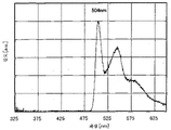
도 20은 2mDBTPDBq-II (약어)의 인광 스펙트럼을 나타낸다.
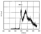
도 21은 PCBA1BP (약어)의 인광 스펙트럼을 나타낸다.
도 22는 BPAFLP (약어)의 인광 스펙트럼을 나타낸다.1 shows a light emitting device according to an embodiment of the present invention.
2A and 2B show the concept of one embodiment of the present invention.
3 shows the energy levels of one molecule of DBq (abbreviation), one molecule of TPA (abbreviation), and a dimer of DBq (abbreviation) and TPA (abbreviation).
4(A) to 4(F) show the distribution of HOMO and LUMO of DBq (abbreviation) 1 molecule, TPA (abbreviation) 1 molecule, and a dimer of DBq (abbreviation) and TPA (abbreviation), respectively. .
5A to 5C show the concept of energy levels of the hole transport layer and the light emitting layer according to one embodiment of the present invention.
6 shows a light emitting device according to an embodiment of the present invention.
7A and 7B show the structure of the light emitting device.
8 shows the structure of a light emitting device.
9A and 9B show a light emitting device.
10A to 10D show electronic devices.
11A to 11D show electronic devices.
12A to 12C show a lighting device.
13 shows the structure of a light emitting device in the embodiment.
14 shows the luminance versus current density characteristics of the light emitting device described in Example 1. FIG.
15 shows the luminance versus voltage characteristics of the light emitting device described in Example 1. FIG.
16 shows the current efficiency versus luminance characteristics of the light emitting device described in Example 1. FIG.
17 shows the current versus voltage characteristics of the light emitting device described in Example 1. FIG.
18 shows the emission spectrum of the light emitting device described in Example 1. FIG.
19 shows the power efficiency versus luminance characteristics of the light emitting device in Example 1. FIG.
20 shows the phosphorescence spectrum of 2mDBTPDBq-II (abbreviated).
21 shows the phosphorescence spectrum of PCBA1BP (abbreviated).
22 shows the phosphorescence spectrum of BPAFLP (abbreviated).
발명을 실시하기 위한 최선의 형태Best Mode for Carrying Out the Invention
이하, 본 발명의 실시형태를 첨부된 도면을 참조로 하여 상세히 설명할 것이다. 본 발명은 하기 기재로 제한되지 않으며, 그의 형태 및 상세사항은 본 발명의 취지 및 범위로부터 벗어나지 않으면서 다양한 방식으로 변화될 수 있음을 인지한다. 따라서, 본 발명은 하기 실시형태의 기재로 제한되는 것으로 해석되어선 안된다.DETAILED DESCRIPTION OF THE PREFERRED EMBODIMENTS Hereinafter, embodiments of the present invention will be described in detail with reference to the accompanying drawings. It is recognized that the present invention is not limited to the following description, and its form and details may be changed in various ways without departing from the spirit and scope of the present invention. Accordingly, the present invention should not be construed as being limited to the description of the following embodiments.
도면 등에 나타낸 각 구성요소의 위치, 크기, 범위 등은, 용이한 이해를 위해 일부 경우에 정확하게 표시되지 않았음을 인지한다. 따라서, 개시된 발명은 도면 등에 개시된 위치, 크기, 범위 등으로 반드시 제한되지는 않는다.It is recognized that the position, size, range, etc. of each component shown in the drawings and the like are not accurately indicated in some cases for easy understanding. Accordingly, the disclosed invention is not necessarily limited to the position, size, scope, etc. disclosed in the drawings and the like.
본 명세서 등에서, "제1", "제2" 및 "제3" 등의 서수는 구성요소들간의 혼동을 피하기 위해 사용된 것이며, 구성요소를 수적으로 제한하는 것은 아니다.In this specification and the like, ordinal numbers such as “first”, “second”, and “third” are used to avoid confusion between components, and do not limit the number of components.
(실시형태 1) (Embodiment 1)
본 실시형태에서는, 본 발명의 하나의 실시형태인 발광 소자의 구조적 개념 및 발광 소자의 구체적 구조를 설명할 것이다. 먼저, 본 발명의 하나의 실시형태인 발광 소자의 소자 구조를 도 1을 참조로 하여 설명할 것이다.In this embodiment, the structural concept of the light emitting element and the specific structure of the light emitting element which are one embodiment of the present invention will be described. First, the device structure of a light emitting device according to an embodiment of the present invention will be described with reference to FIG. 1 .
도 1에 나타낸 소자 구조는, 한 쌍의 전극 (제1 전극(101) 및 제2 전극(103)) 사이에, 정공 수송 층(112) 및 정공 수송 층(112) 위의 발광 층(113)을 포함한다. 발광 층(113)은 전자 수송성을 갖는 제1 유기 화합물(120), 정공 수송성을 갖는 제2 유기 화합물(122), 및 삼중항 여기 에너지를 발광으로 변환시키는 발광성의 제3 유기 화합물(124)을 함유한다. 제1 유기 화합물(120)과 제2 유기 화합물(122)의 조합은 엑시플렉스를 형성한다. 정공 수송 층(112)은 적어도, HOMO 준위가 제2 유기 화합물(122)의 HOMO 준위 이하인 제4 유기 화합물(126) 및 HOMO 준위가 제2 유기 화합물(122)의 HOMO 준위보다 높은 제5 유기 화합물(128)을 함유한다.The device structure shown in FIG. 1 is between a pair of electrodes (a
도 1에서, 제1 전극(101)과 정공 수송 층(112) 사이의 영역에는 필요한 경우 정공 주입 층 또는 정공 수송 층이 형성될 수 있음을 인지한다. 또한, 도 1에서, 제2 전극(103)과 발광 층(113) 사이의 영역에는 필요한 경우 전자 주입 층 또는 전자 수송 층이 형성될 수 있다.In FIG. 1 , it is recognized that a hole injection layer or a hole transport layer may be formed in a region between the
제1 유기 화합물(120)이 호스트 재료로서 사용되고, 제2 유기 화합물(122)이 어시스트 재료로서 사용되고, 제3 유기 화합물(124)이 게스트 재료로서 사용되는 것이 바람직함을 인지한다. 즉, 발광 층 내의 제3 유기 화합물의 질량 분율 (또는 부피 분율)은 바람직하게는 제1 유기 화합물 및 제2 유기 화합물 각각의 질량 분율보다 낮다. 하기 기재에서는, 일부 경우에, 제1 유기 화합물(120), 제2 유기 화합물(122), 및 제3 유기 화합물(124)을 각각 호스트 재료, 어시스트 재료, 및 게스트 재료로서 언급한다.It is recognized that it is preferable that the first
예를 들어, 10-6 ㎠/Vs 이상의 전자 이동도를 갖는 전자 수송 재료가 제1 유기 화합물(120) (호스트 재료)로서 사용될 수 있다. 또한, 예를 들어, 10-6 ㎠/Vs 이상의 정공 이동도를 갖는 정공 수송 재료가 제2 유기 화합물(122) (어시스트 재료)로서 사용될 수 있다.For example, an electron transporting material having an electron mobility of 10 −6
상기 구조에서, 제1 유기 화합물(120) (호스트 재료) 및 제2 유기 화합물(122) (어시스트 재료) 각각의 최저 삼중항 여기 에너지 준위 (T1 준위)는 바람직하게는 제3 유기 화합물(124) (게스트 재료)의 T1 준위보다 높음을 인지한다. 그 이유는 하기와 같다: 제1 유기 화합물(120) (호스트 재료) 및 제2 유기 화합물(122) (어시스트 재료) 각각의 T1 준위가 제3 유기 화합물(124) (게스트 재료)의 T1 준위보다 낮으면, 발광에 기여하는 제3 유기 화합물(124) (게스트 재료)의 삼중항 여기 에너지가 제1 유기 화합물(120) (호스트 재료) 및 제2 유기 화합물(122) (어시스트 재료)에 의해 소광되며, 이는 발광 효율을 감소시킨다.In the above structure, the lowest triplet excitation energy level (T 1 level) of each of the first organic compound 120 (host material) and the second organic compound 122 (assist material) is preferably the third organic compound 124 ) (guest material) above the T 1 level. The reason is as follows: the
또한, 호스트 재료로부터 게스트 재료로의 에너지 전달의 효율 향상을 위해서는, 분자간의 에너지 전달 메커니즘으로서 공지된 포스터(Foerster) 메커니즘 (쌍극자-쌍극자 상호작용) 및 덱스터(Dexter) 메커니즘 (전자 교환 상호작용)이 고려된다. 이들 메커니즘에 따르면, 호스트 재료의 발광 스펙트럼 (일중항 여기 상태로부터의 에너지 전달에서는 형광 스펙트럼, 삼중항 여기 상태로부터의 에너지 전달에서는 인광 스펙트럼)이 게스트 재료의 흡수 스펙트럼 (구체적으로는, 최장파장 (최저 에너지)측의 흡수 밴드에서의 스펙트럼)과 크게 중첩되는 것이 바람직하다.In addition, in order to improve the efficiency of energy transfer from the host material to the guest material, the Foerster mechanism (dipole-dipole interaction) and Dexter mechanism (electron exchange interaction), which are known as intermolecular energy transfer mechanisms, are are considered According to these mechanisms, the emission spectrum of the host material (fluorescence spectrum in energy transfer from singlet excited state, phosphorescence spectrum in energy transfer from triplet excited state) of the guest material (specifically, the longest wavelength (lowest wavelength) It is preferable that the spectrum in the absorption band on the energy side) greatly overlap.
그러나, 예를 들어, 게스트 재료로서 인광성 화합물을 사용하는 경우에는, 호스트 재료의 형광 스펙트럼과 게스트 재료의 최장파장 (최저 에너지)측의 흡수 밴드에서의 흡수 스펙트럼 사이의 중첩을 얻기가 어렵다. 그 이유는 하기와 같다: 호스트 재료의 형광 스펙트럼이 게스트 재료의 최장파장 (최저 에너지)측의 흡수 밴드에서의 흡수 스펙트럼과 중첩되는 경우, 호스트 재료의 인광 스펙트럼이 형광 스펙트럼에 비해 보다 장파장 (보다 낮은 에너지)측에 위치하기 때문에, 호스트 재료의 T1 준위가 인광성 화합물의 T1 준위보다 낮게 되고, 상기에 기재된 소광 문제가 발생되지만; 소광 문제를 피하기 위해, 호스트 재료를, 호스트 재료의 T1 준위가 게스트 재료로서 사용되는 인광성 화합물의 T1 준위보다 높게 되도록 설계하면, 호스트 재료의 형광 스펙트럼이 보다 단파장 (보다 높은 에너지)측으로 변위되고, 따라서 형광 스펙트럼이 게스트 재료의 최장파장 (최저 에너지)측의 흡수 밴드에서의 흡수 스펙트럼과 어떠한 중첩도 갖지 않는다. 이러한 이유로, 일반적으로, 호스트 재료의 형광 스펙트럼과 게스트 재료의 최장파장 (최저 에너지)측의 흡수 밴드에서의 흡수 스펙트럼 사이의 중첩을 얻어 호스트 재료의 일중항 여기 상태로부터의 에너지 전달을 최대화하는 것은 어렵다.However, for example, when a phosphorescent compound is used as the guest material, it is difficult to obtain overlap between the fluorescence spectrum of the host material and the absorption spectrum in the absorption band on the longest wavelength (lowest energy) side of the guest material. The reason is as follows: when the fluorescence spectrum of the host material overlaps with the absorption spectrum in the absorption band on the longest wavelength (lowest energy) side of the guest material, the phosphorescence spectrum of the host material has a longer wavelength (lower energy) than the fluorescence spectrum. energy) side, the T 1 level of the host material becomes lower than the T 1 level of the phosphorescent compound, and the quenching problem described above occurs; In order to avoid the quenching problem, if the host material is designed such that the T 1 level of the host material is higher than the T 1 level of the phosphorescent compound used as the guest material, the fluorescence spectrum of the host material is shifted toward the shorter wavelength (higher energy) side. Therefore, the fluorescence spectrum does not have any overlap with the absorption spectrum in the absorption band on the longest wavelength (lowest energy) side of the guest material. For this reason, in general, it is difficult to obtain an overlap between the fluorescence spectrum of the host material and the absorption spectrum in the absorption band on the longest wavelength (lowest energy) side of the guest material to maximize energy transfer from the singlet excited state of the host material. .
따라서, 본 발명의 하나의 실시형태에서, 제1 유기 화합물(120)과 제2 유기 화합물(122)의 조합은 엑시플렉스 (또한 여기 착체로서 언급됨)를 형성한다. 엑시플렉스를 도 2의 (A) 및 도 2의 (B)를 참조로 하여 하기에서 설명할 것이다.Thus, in one embodiment of the present invention, the combination of the first
도 2의 (A)는 엑시플렉스의 개념을 나타내는 개략도이고; 제1 유기 화합물(120) (또는 제2 유기 화합물(122))의 형광 스펙트럼, 제1 유기 화합물(120) (또는 제2 유기 화합물(122))의 인광 스펙트럼, 제3 유기 화합물(124)의 흡수 스펙트럼, 및 엑시플렉스의 발광 스펙트럼이 나타나 있다.Figure 2 (A) is a schematic diagram showing the concept of the exciplex; The fluorescence spectrum of the first organic compound 120 (or the second organic compound 122), the phosphorescence spectrum of the first organic compound 120 (or the second organic compound 122), and the third
예를 들어, 발광 층(113)에서, 제1 유기 화합물(120) (호스트 재료)의 형광 스펙트럼 및 제2 유기 화합물(122) (어시스트 재료)의 형광 스펙트럼은 보다 장파장측에 위치하는 엑시플렉스의 발광 스펙트럼으로 변환된다. 또한, 엑시플렉스의 발광 스펙트럼이 제3 유기 화합물(124) (게스트 재료)의 흡수 스펙트럼과 크게 중첩되도록 제1 유기 화합물(120) (호스트 재료) 및 제2 유기 화합물(122) (어시스트 재료)을 선택하는 것은, 일중항 여기 상태로부터의 에너지 전달이 최대화될 수 있게 한다 (도 2의 (A) 참조).For example, in the
또한, 삼중항 여기 상태의 경우에는, 호스트 재료가 아닌 엑시플렉스로부터의 에너지 전달이 일어나는 것으로 고려됨을 인지한다.It is also recognized that in the case of triplet excited states, energy transfer is considered to occur from the exciplex rather than the host material.
따라서, 형성된 엑시플렉스의 발광 파장이 제1 유기 화합물(120) (호스트 재료) 및 제2 유기 화합물(122) (어시스트 재료) 각각의 발광 파장 (형광 파장)보다 길기 때문에, 제1 유기 화합물(120) (호스트 재료)의 형광 스펙트럼 또는 제2 유기 화합물(122) (어시스트 재료)의 형광 스펙트럼이 보다 장파장측에 위치하는 발광 스펙트럼이 될 수 있다.Therefore, since the emission wavelength of the formed exciplex is longer than the emission wavelength (fluorescence wavelength) of each of the first organic compound 120 (host material) and the second organic compound 122 (assist material), the first organic compound 120 ) (host material) or the fluorescence spectrum of the second organic compound 122 (assist material) may be an emission spectrum located on the longer wavelength side.
또한, 엑시플렉스는 아마도 일중항 여기 에너지와 삼중항 여기 에너지 사이에 극히 작은 차이를 가질 것이다. 즉, 일중항 상태로부터의 엑시플렉스의 발광 스펙트럼 및 삼중항 상태로부터의 그의 발광 스펙트럼이 서로 매우 근접해 있다. 따라서, 상기에 기재된 바와 같이 엑시플렉스의 발광 스펙트럼 (일반적으로 일중항 상태로부터의 엑시플렉스의 발광 스펙트럼)이 최장파장측에 위치하는 제3 유기 화합물(124) (게스트 재료)의 흡수 밴드와 중첩되도록 설계를 수행하는 경우, 삼중항 상태로부터의 엑시플렉스의 발광 스펙트럼 (이는 많은 경우에 실온에서 관찰되지 않고 저온에서도 관찰되지 않음)이 또한 최장파장측에 위치하는 제3 유기 화합물(124) (게스트 재료)의 흡수 밴드와 중첩된다. 즉, 삼중항 여기 상태로부터의 에너지 전달의 효율 뿐만 아니라 일중항 여기 상태로부터의 에너지 전달의 효율이 증가할 수 있고, 그 결과, 일중항 및 삼중항 여기 상태 둘 다로부터 발광이 효율적으로 얻어질 수 있다.Also, the exciplex probably has an extremely small difference between the singlet excitation energy and the triplet excitation energy. That is, the emission spectrum of exciplex from the singlet state and the emission spectrum thereof from the triplet state are very close to each other. Therefore, as described above, the emission spectrum of the exciplex (generally the emission spectrum of the exciplex from the singlet state) overlaps with the absorption band of the third organic compound 124 (guest material) located on the longest wavelength side. When carrying out the design, the emission spectrum of the exciplex from the triplet state (which in many cases is not observed at room temperature and not even at low temperature) is also found in the third
상기에 기재된 바와 같이, 본 발명의 하나의 실시형태의 발광 소자에서는, 발광 층(113)에 형성된 엑시플렉스의 발광 스펙트럼과 제3 유기 화합물(124) (게스트 재료)의 흡수 스펙트럼 사이의 중첩을 이용하여 에너지가 전달되고; 따라서, 에너지 전달 효율이 높다.As described above, in the light emitting device of one embodiment of the present invention, the overlap between the emission spectrum of the exciplex formed in the
또한, 엑시플렉스는 여기 상태로만 존재하고, 따라서 에너지를 흡수할 수 있는 기저 상태를 갖지 않는다. 따라서, 제3 유기 화합물(124) (게스트 재료)의 일중항 여기 상태 및 삼중항 여기 상태로부터 엑시플렉스로의 에너지 전달에 의해 제3 유기 화합물(124) (게스트 재료)이 발광 전에 실활되는 (즉, 발광 효율이 감소됨) 현상은 아마도 원칙적으로 발생하지 않을 것이다.Also, exciplexes exist only in excited states and therefore do not have a ground state capable of absorbing energy. Therefore, by energy transfer from the singlet excited state and the triplet excited state to the exciplex of the third organic compound 124 (guest material), the third organic compound 124 (guest material) is deactivated before light emission (i.e. , the luminous efficiency is reduced), which probably does not occur in principle.
상기에 기재된 엑시플렉스는 여기 상태의 상이한 분자들간의 상호작용에 의해 형성됨을 인지한다. 엑시플렉스는 일반적으로, 비교적 낮은 LUMO (LUMO: 최저 비점유 분자 오비탈) 준위를 갖는 재료와 비교적 높은 HOMO (HOMO: 최고 점유 분자 오비탈) 준위를 갖는 재료 사이에서 용이하게 형성되는 것으로 공지되어 있다.It is recognized that the exciplexes described above are formed by interactions between different molecules in an excited state. Exciplexes are generally known to form readily between materials having a relatively low LUMO (LUMO: lowest unoccupied molecular orbital) level and a material having a relatively high HOMO (HOMO: highest occupied molecular orbital) level.
여기서, 제1 유기 화합물(120), 제2 유기 화합물(122), 및 엑시플렉스의 에너지 준위의 개념을 도 2의 (B)를 참조로 하여 설명한다. 도 2의 (B)는 제1 유기 화합물(120), 제2 유기 화합물(122), 및 엑시플렉스의 에너지 준위를 개략적으로 나타내는 것임을 인지한다.Here, the concept of the energy level of the first
제1 유기 화합물(120) (호스트 재료) 및 제2 유기 화합물(122) (어시스트 재료)의 HOMO 준위 및 LUMO 준위는 서로 상이하다. 구체적으로는, 에너지 준위는 하기 순서로 달라진다: 제1 유기 화합물(120)의 HOMO 준위 < 제2 유기 화합물(122)의 HOMO 준위 < 제1 유기 화합물(120)의 LUMO 준위 < 제2 유기 화합물(122)의 LUMO 준위. 엑시플렉스가 이들 두 유기 화합물에 의해 형성되는 경우, 엑시플렉스의 LUMO 준위 및 HOMO 준위는 각각 제1 유기 화합물(120) (호스트 재료) 및 제2 유기 화합물(122) (어시스트 재료)로부터 유래된다 (도 2의 (B) 참조). The HOMO level and LUMO level of the first organic compound 120 (host material) and the second organic compound 122 (assist material) are different from each other. Specifically, the energy level varies in the following order: HOMO level of the first
엑시플렉스의 발광 파장은 HOMO 준위와 LUMO 준위 사이의 에너지 차에 의존한다. 일반적 경향으로, 에너지 차가 크면, 발광 파장이 짧고, 에너지 차가 작으면, 발광 파장이 길다.The emission wavelength of exciplex depends on the energy difference between the HOMO level and the LUMO level. In general, when the energy difference is large, the emission wavelength is short, and when the energy difference is small, the emission wavelength is long.
따라서, 엑시플렉스의 에너지 차는 제1 유기 화합물(120) (호스트 재료)의 에너지 차 및 제2 유기 화합물(122) (어시스트 재료)의 에너지 차보다 작다. 즉, 엑시플렉스의 발광 파장은 제1 유기 화합물(120) 및 제2 유기 화합물(122) 각각의 발광 파장보다 길다.Therefore, the energy difference of Exciplex is smaller than the energy difference of the first organic compound 120 (host material) and the energy difference of the second organic compound 122 (assist material). That is, the emission wavelength of the exciplex is longer than the emission wavelength of each of the first
엑시플렉스가 실제로 이러한 특성을 갖는지의 여부를 확인하기 위해 분자 오비탈 계산을 하기와 같이 수행하였다. 일반적으로, 헤테로방향족 화합물과 방향족 아민의 조합은 종종, 방향족 아민의 LUMO 준위보다 낮은 헤테로방향족 화합물의 LUMO 준위 (전자를 쉽게 수용하는 특성) 및 헤테로방향족 화합물의 HOMO 준위보다 높은 방향족 아민의 HOMO 준위 (정공을 쉽게 수용하는 특성)의 영향 하에 엑시플렉스를 형성한다. 따라서, 헤테로방향족 화합물의 LUMO를 형성하는 전형적인 골격이며 본 발명의 하나의 실시형태에서의 제1 유기 화합물(120)의 모델인 디벤조[f,h]퀴녹살린 (약어: DBq)과, 방향족 아민의 HOMO를 형성하는 전형적인 골격이며 본 발명의 하나의 실시형태에서의 제2 유기 화합물(122)의 모델인 트리페닐아민 (약어: TPA)의 조합을 사용하여 계산을 수행하였다.Molecular orbital calculations were performed as follows to confirm whether Exciplex actually has these properties. In general, the combination of a heteroaromatic compound and an aromatic amine often results in a lower LUMO level of the heteroaromatic compound (a property of easily accepting electrons) than the LUMO level of the aromatic amine and a higher HOMO level of the aromatic amine than the HOMO level of the heteroaromatic compound ( It forms an exciplex under the influence of the property of easily accepting holes). Accordingly, dibenzo[f,h]quinoxaline (abbreviation: DBq), which is a typical skeleton forming the LUMO of heteroaromatic compounds and is a model of the first
먼저, 최저 일중항 여기 상태 (S1) 및 최저 삼중항 여기 상태 (T1)에서의 DBq (약어) 1 분자 및 TPA (약어) 1 분자의 최적 분자 구조 및 여기 에너지를, 시간-의존 밀도 함수 이론 (TD-DFT)을 이용하여 계산하였다. 또한, DBq (약어)와 TPA (약어)의 이량체의 여기 에너지를 또한 계산하였다.First, the optimal molecular structure and excitation energy of 1 molecule of DBq (abbreviated) and 1 molecule of TPA (abbreviated) in the lowest singlet excited state (S 1 ) and lowest triplet excited state (T 1 ) are obtained as a time-dependent density function. It was calculated using theory (TD-DFT). In addition, the excitation energies of the dimers of DBq (abbreviation) and TPA (abbreviation) were also calculated.
밀도 함수 이론 (DFT)에서, 총 에너지는 위치 에너지, 전자간 정전 에너지, 전자 운동 에너지, 및 복잡한 전자간 상호작용을 모두 포함하는 교환-상관 에너지의 합계로서 나타내어진다. 또한 DFT에서는, 교환-상관 상호작용이, 전자 밀도로 표시되는 하나의 전자 전위의 함수 (또 다른 함수의 함수)로 근사되어, 높은 속도 및 높은 정확도의 계산을 가능하게 한다. 여기서는, 하이브리드 함수인 B3LYP를 이용하여 교환-상관 에너지에 관한 각각의 파라미터의 무게를 특정하였다.In density functional theory (DFT), total energy is expressed as the sum of exchange-correlated energies including potential energy, interelectron electrostatic energy, electron kinetic energy, and complex interelectron interactions. Also in DFT, the exchange-correlation interaction is approximated as a function of one electron potential expressed as electron density (a function of another function), enabling high-speed and high-accuracy calculations. Here, the weight of each parameter regarding the exchange-correlation energy was specified using the hybrid function B3LYP.
또한, 기저 함수로서, 6-311 (각각의 원자가 오비탈에 대한 3개의 단축 함수를 사용하는 3중-분할 원자가(triple-split valence) 기저계의 기저 함수)을 모든 원자에 적용하였다.Also, as a basis function, 6-311 (a basis function of a triple-split valence basis system using three uniaxial functions for each valence orbital) was applied to all atoms.
상기 기저 함수에 의해, 예를 들어, 수소 원자의 경우에는 1s 내지 3s 오비탈이 고려되며, 탄소 원자의 경우에는 1s 내지 4s 및 2p 내지 4p 오비탈이 고려된다. 또한, 계산 정확도를 향상시키기 위해, 분극 기저계로서 p 함수 및 d 함수를 각각 수소 원자 및 수소 원자 이외의 원자에 가하였다.By the basis function, for example, 1s to 3s orbitals are considered for a hydrogen atom, and 1s to 4s and 2p to 4p orbitals are considered for a carbon atom. In addition, in order to improve the calculation accuracy, a p function and a d function as a polarization basis system were applied to a hydrogen atom and an atom other than the hydrogen atom, respectively.
양자 화학 계산 프로그램으로서는 가우시안(Gaussian) 09를 사용하였음을 인지한다. 고성능 컴퓨터 (알틱스(Altix) 4700, 에스지아이 재팬, 리미티드(SGI Japan, Ltd.) 제조)를 계산에 사용하였다.It is recognized that Gaussian 09 was used as a quantum chemistry calculation program. A high-performance computer (Altix 4700, manufactured by SGI Japan, Ltd.) was used for calculation.
먼저, DBq (약어) 1 분자, TPA (약어) 1 분자, 및 DBq (약어)와 TPA (약어)의 이량체의 HOMO 준위 및 LUMO 준위를 계산하였다. 도 3에 HOMO 준위 및 LUMO 준위를 나타내었다.First, the HOMO level and LUMO level of one molecule of DBq (abbreviation), one molecule of TPA (abbreviation), and a dimer of DBq (abbreviation) and TPA (abbreviation) were calculated. 3 shows the HOMO level and the LUMO level.
도 3에 나타낸 바와 같이, DBq (약어)와 TPA (약어)의 이량체는, TPA (약어)의 LUMO 준위보다 낮은 DBq (약어)의 LUMO 준위 (-1.99 eV) 및 DBq (약어)의 HOMO 준위보다 높은 TPA (약어)의 HOMO 준위 (-5.21 eV)의 영향 하에 DBq (약어) 및 TPA (약어)의 엑시플렉스를 형성한다는 것이 시사된다.As shown in Fig. 3, the dimer of DBq (abbreviation) and TPA (abbreviation) has a lower LUMO level of DBq (abbreviation) than the LUMO level of TPA (abbreviation) (-1.99 eV) and HOMO level of DBq (abbreviation). It is suggested to form exciplexes of DBq (abbreviation) and TPA (abbreviation) under the influence of the HOMO level (-5.21 eV) of higher TPA (abbreviation).
도 4의 (A) 내지 도 4의 (F)는 DBq (약어) 1 분자, TPA (약어) 1 분자, 및 DBq (약어)와 TPA (약어)의 이량체의 HOMO 및 LUMO의 분포를 나타낸다.4A to 4F show the distribution of HOMO and LUMO of one molecule of DBq (abbreviation), one molecule of TPA (abbreviation), and a dimer of DBq (abbreviation) and TPA (abbreviation).
도 4의 (A)는 DBq (약어) 1 분자의 LUMO 분포를 나타내고, 도 4의 (B)는 DBq 1 분자의 HOMO 분포를 나타내고, 도 4의 (C)는 TPA (약어) 1 분자의 LUMO 분포를 나타내고, 도 4의 (D)는 TPA (약어) 1 분자의 HOMO 분포를 나타내고, 도 4의 (E)는 DBq (약어)와 TPA (약어)의 이량체의 LUMO 분포를 나타내고, 도 4의 (F)는 DBq (약어)와 TPA (약어)의 이량체의 HOMO 분포를 나타냄을 인지한다.Fig. 4(A) shows the LUMO distribution of one molecule of DBq (abbreviation), Fig. 4(B) shows the HOMO distribution of one molecule of DBq, and Fig. 4(C) shows the LUMO of one molecule of TPA (abbreviation). Figure 4 (D) shows the HOMO distribution of one molecule of TPA (abbreviation), Figure 4 (E) shows the LUMO distribution of a dimer of DBq (abbreviation) and TPA (abbreviation), Figure 4 Note that (F) in (F) represents the HOMO distribution of a dimer of DBq (abbreviation) and TPA (abbreviation).
도 4의 (E) 및 도 4의 (F)에 나타낸 바와 같이, DBq (약어)와 TPA (약어)의 이량체의 LUMO는 DBq (약어)측에 분포하고, 그의 HOMO는 TPA (약어)측에 분포하고, 이는 도 3에 나타낸 결과와 일치한다.As shown in Fig. 4(E) and Fig. 4(F), the LUMO of the dimer of DBq (abbreviation) and TPA (abbreviation) is distributed on the DBq (abbreviation) side, and its HOMO is on the TPA (abbreviation) side. , which is consistent with the results shown in Fig.
본 발명의 하나의 실시형태에서의 엑시플렉스의 형성 방법은, 하기에 기재되는 두가지 방법 중 어느 한쪽일 수 있다.The method of forming exciplex in one embodiment of the present invention may be any one of the two methods described below.
하나의 엑시플렉스 형성 방법은, 캐리어(양이온 또는 음이온)를 갖는 제1 유기 화합물(120) (호스트 재료) 및 제2 유기 화합물(122)(어시스트 재료)로부터 엑시플렉스를 형성하는 것이다.One exciplex formation method is to form an exciplex from a first organic compound 120 (host material) and a second organic compound 122 (assist material) having a carrier (cation or anion).
일반적으로는, 전자 및 정공이 호스트 재료 중에서 재결합되는 경우, 여기 상태의 호스트 재료로부터 게스트 재료로 여기 에너지가 전달되고, 따라서 게스트 재료가 여기 상태가 되어 발광하게 된다. 호스트 재료로부터 게스트 재료로 여기 에너지가 전달되기 전에, 호스트 재료 자체가 발광하거나 여기 에너지가 열 에너지로 전환되고, 이는 여기 에너지의 부분적 실활을 초래한다.In general, when electrons and holes recombine in a host material, excitation energy is transferred from the host material in an excited state to the guest material, so that the guest material enters an excited state and emits light. Before the excitation energy is transferred from the host material to the guest material, the host material itself emits light or the excitation energy is converted into thermal energy, which results in partial deactivation of the excitation energy.
그러나, 본 발명의 하나의 실시형태에서는, 캐리어 (양이온 또는 음이온)를 갖는 제1 유기 화합물(120) (호스트 재료) 및 제2 유기 화합물(122) (어시스트 재료)로부터 엑시플렉스가 형성되고; 따라서, 제1 유기 화합물(120) (호스트 재료)의 일중항 엑시톤의 형성이 억제될 수 있다. 즉, 일중항 엑시톤을 형성하지 않으면서 직접 엑시플렉스를 형성하는 방법이 존재할 수 있다. 따라서, 일중항 여기 에너지의 실활이 억제될 수 있다. 따라서, 긴 수명을 갖는 발광 소자가 얻어질 수 있다.However, in one embodiment of the present invention, exciplex is formed from a first organic compound 120 (host material) and a second organic compound 122 (assist material) having a carrier (cation or anion); Accordingly, the formation of singlet excitons of the first organic compound 120 (host material) can be suppressed. That is, there may be a method of directly forming an exciplex without forming a singlet exciton. Therefore, the deactivation of singlet excitation energy can be suppressed. Accordingly, a light emitting element having a long lifetime can be obtained.
예를 들어, 제1 유기 화합물(120)이 전자 수송 재료 중 전자 (캐리어)를 쉽게 포획하는 특성을 갖는 (낮은 LUMO 준위를 갖는) 전자 트랩핑 화합물이고, 제2 유기 화합물(122)이 정공 수송 재료 중 정공 (캐리어)을 쉽게 포획하는 특성을 갖는 (높은 HOMO 준위를 갖는) 정공 트랩핑 화합물인 경우에는, 제1 유기 화합물(120)의 음이온 및 제2 유기 화합물(122)의 양이온으로부터 직접 엑시플렉스가 형성된다. 이러한 방법을 통해 형성된 엑시플렉스는 특히 일렉트로플렉스(electroplex)로서 언급된다. For example, the first
상기에 기재된 방식으로, 제1 유기 화합물(120) (호스트 재료)의 일중항 여기 상태의 생성을 억제하고, 일렉트로플렉스로부터 제3 유기 화합물(124) (게스트 재료)로 에너지를 전달함으로써, 높은 발광 효율을 갖는 발광 소자가 얻어질 수 있다. 이 경우, 제1 유기 화합물(120) (호스트 재료)의 삼중항 여기 상태의 생성도 유사하게 억제되고, 직접 엑시플렉스가 형성되고; 따라서, 아마도 엑시플렉스로부터 제3 유기 화합물(124) (게스트 재료)로의 에너지 전달이 일어날 것임을 인지한다.In the manner described above, by suppressing the generation of a singlet excited state of the first organic compound 120 (host material) and transferring energy from the electroplex to the third organic compound 124 (guest material), high luminescence A light emitting element with efficiency can be obtained. In this case, the generation of the triplet excited state of the first organic compound 120 (host material) is similarly suppressed, and a direct exciplex is formed; Accordingly, it is recognized that energy transfer will likely occur from the exciplex to the third organic compound 124 (guest material).
다른 엑시플렉스 형성 방법은, 제1 유기 화합물(120) (호스트 재료) 및 제2 유기 화합물(122) (어시스트 재료) 중 하나가 일중항 엑시톤을 형성하고, 이어서 기저 상태의 다른 하나와 상호작용하여 엑시플렉스를 형성하는 기본적 방법이다. 일렉트로플렉스와 달리, 이 경우에는 일시적으로 제1 유기 화합물(120) (호스트 재료) 또는 제2 유기 화합물(122) (어시스트 재료)의 일중항 여기 상태가 생성되지만, 이는 엑시플렉스로 빠르게 전환되고; 따라서, 일중항 여기 에너지의 실활이 억제될 수 있다. 따라서, 제1 유기 화합물(120) 또는 제2 유기 화합물(122)의 여기 에너지의 실활을 억제할 수 있다. 이 경우, 아마도, 제1 유기 화합물(120) (호스트 재료)의 삼중항 여기 상태도 유사하게 엑시플렉스로 빠르게 전환되고, 엑시플렉스로부터 제3 유기 화합물(124) (게스트 재료)로 에너지가 전달될 것임을 인지한다.Another method of exciplex formation is that one of the first organic compound 120 (host material) and the second organic compound 122 (assist material) forms a singlet exciton and then interacts with the other in the ground state This is a basic method of forming an exciplex. Unlike electroflex, in this case a singlet excited state of either the first organic compound 120 (host material) or the second organic compound 122 (assist material) is temporarily created in this case, but it is rapidly converted to exciplex; Therefore, the deactivation of singlet excitation energy can be suppressed. Accordingly, deactivation of the excitation energy of the first
제1 유기 화합물(120) (호스트 재료)이 전자 트랩핑 화합물이고, 제2 유기 화합물(122) (어시스트 재료)이 정공 트랩핑 화합물이고, 이들 화합물의 HOMO 준위간 차이 및 LUMO 준위간 차이가 큰 (구체적으로는, 0.3 eV 이상) 경우, 전자는 선택적으로 제1 유기 화합물(120) (호스트 재료)로 주입되고, 정공은 선택적으로 제2 유기 화합물(122) (어시스트 재료)로 주입됨을 인지한다. 이 경우, 일중항 엑시톤을 통해 엑시플렉스가 형성되는 방법에 비해 일렉트로플렉스가 형성되는 방법이 아마도 우선적일 것이다.The first organic compound 120 (host material) is an electron trapping compound, and the second organic compound 122 (assist material) is a hole trapping compound, and the difference between the HOMO and LUMO levels of these compounds is large. (specifically, 0.3 eV or more), it is recognized that electrons are selectively injected into the first organic compound 120 (host material), and holes are selectively injected into the second organic compound 122 (assist material) . In this case, the method in which the electroplex is formed is probably preferred over the method in which the exciplex is formed through a singlet exciton.
다음으로, 여기 에너지의 계산 결과를 나타낸다. DBq (약어) 1 분자의 S1 여기 에너지는 3.294 eV이고, 형광 파장은 376.4 nm이다. DBq (약어) 1 분자의 T1 여기 에너지는 2.460 eV이고, 인광 파장은 504.1 nm이다. 한편, TPA (약어) 1 분자의 S1 여기 에너지는 3.508 eV이고, 형광 파장은 353.4 nm이다. TPA (약어) 1 분자의 T1 여기 에너지는 2.610 eV이고, 인광 파장은 474.7 nm이다.Next, the calculation result of the excitation energy is shown. The S 1 excitation energy of one molecule of DBq (abbreviation) is 3.294 eV, and the fluorescence wavelength is 376.4 nm. The T 1 excitation energy of one molecule of DBq (abbreviation) is 2.460 eV, and the phosphorescence wavelength is 504.1 nm. On the other hand, the S 1 excitation energy of one molecule of TPA (abbreviation) is 3.508 eV, and the fluorescence wavelength is 353.4 nm. T 1 excitation energy of one molecule of TPA (abbreviation) is 2.610 eV, and the phosphorescence wavelength is 474.7 nm.
여기서는, S1 및 T1 준위에서의 DBq (약어)와 TPA (약어)의 이량체의 최적 분자 구조로부터 얻어지는 여기 에너지를 나타낸다. DBq (약어)와 TPA (약어)의 이량체의 S1 여기 에너지는 2.036 eV이고, 형광 파장은 609.1 nm이다. DBq (약어)와 TPA (약어)의 이량체의 T1 여기 에너지는 2.030 eV이고, 인광 파장은 610.0 nm이다.Here, the excitation energy obtained from the optimal molecular structure of the dimer of DBq (abbreviation) and TPA (abbreviation) at the S 1 and T 1 levels is shown. The S 1 excitation energy of the dimer of DBq (abbreviation) and TPA (abbreviation) is 2.036 eV, and the fluorescence wavelength is 609.1 nm. The T 1 excitation energy of the dimer of DBq (abbreviation) and TPA (abbreviation) is 2.030 eV, and the phosphorescence wavelength is 610.0 nm.
상기 내용은, DBq (약어)와 TPA (약어)의 이량체의 형광 파장은 DBq (약어) 1 분자의 형광 파장 및 TPA (약어) 1 분자의 형광 파장보다 길다는 것을 보여준다. 상기 내용은 또한, DBq (약어)와 TPA (약어)의 이량체의 형광 파장과 인광 파장 사이의 차가 단지 0.9 nm이고, 이들 파장은 실질적으로 동일함을 보여준다.The above shows that the fluorescence wavelength of the dimer of DBq (abbreviation) and TPA (abbreviation) is longer than the fluorescence wavelength of one molecule of DBq (abbreviation) and the fluorescence wavelength of one molecule of TPA (abbreviation). The above also shows that the difference between the fluorescence and phosphorescence wavelengths of the dimers of DBq (abbreviation) and TPA (abbreviation) is only 0.9 nm, and these wavelengths are substantially the same.
이들 결과는 엑시플렉스가 일중항 여기 에너지 및 삼중항 여기 에너지를 실질적으로 동일한 에너지로 집약시킬 수 있음을 나타낸다. 따라서, 상기에 기재된 바와 같이, 엑시플렉스는 그의 일중항 상태 및 삼중항 상태 둘 다로부터 인광성 화합물에 에너지를 효율적으로 전달할 수 있다는 것이 시사된다.These results indicate that exciplex can concentrate singlet excitation energy and triplet excitation energy into substantially the same energy. Thus, as described above, it is suggested that exciplex can efficiently transfer energy to phosphorescent compounds from both its singlet and triplet states.
이러한 효과는 에너지 전달 매체로서의 엑시플렉스의 사용에 특이적인 것이다. 일반적으로는, 호스트 재료의 일중항 여기 상태 또는 삼중항 여기 상태로부터 인광성 화합물로의 에너지 전달이 고려된다. 한편, 본 발명의 하나의 실시형태는, 호스트 재료 및 또 다른 재료의 엑시플렉스가 먼저 형성되고, 엑시플렉스로부터의 에너지 전달이 이용된다는 점에서 종래 기술과 큰 차이가 있다. 또한, 이러한 차이는 이례적으로 높은 발광 효율을 제공한다.This effect is specific to the use of Exiplex as an energy transfer medium. In general, energy transfer from a singlet excited state or a triplet excited state of a host material to a phosphorescent compound is contemplated. On the other hand, one embodiment of the present invention is significantly different from the prior art in that an exciplex of a host material and another material is formed first, and energy transfer from the exciplex is used. In addition, this difference provides an exceptionally high luminous efficiency.
일반적으로, 발광 소자의 발광 층에 엑시플렉스를 사용하는 것은, 발광 색을 조절할 수 있는 것 등의 가치를 갖지만, 이는 통상적으로 발광 효율의 현저한 감소를 초래함을 인지한다. 따라서, 엑시플렉스의 사용은 매우 효율적인 발광 소자를 얻기에는 부적합한 것으로 여겨져 왔다. 그러나, 본 발명자들은, 본 발명의 하나의 실시형태에서 나타난 바와 같이, 엑시플렉스를 에너지 전달 매체로서 사용하는 것이, 역으로 발광 효율을 최대화시킬 수 있다는 것을 발견하였다. 이러한 기술적 발상은 종래의 고정 관념과 상반되는 것이다.In general, it is recognized that the use of exciplex in the light emitting layer of a light emitting device has a value such as being able to control the light emitting color, but this usually results in a significant decrease in the luminous efficiency. Therefore, the use of exciplex has been considered inappropriate to obtain a very efficient light emitting device. However, the present inventors have discovered that, as shown in one embodiment of the present invention, the use of exciplex as an energy transfer medium can conversely maximize luminous efficiency. This technical idea is contrary to conventional stereotypes.
엑시플렉스의 발광 스펙트럼과 제3 유기 화합물(124) (게스트 재료)의 흡수 스펙트럼이 서로 충분히 중첩되게 하기 위해서는, 발광 스펙트럼의 피크의 에너지와 흡수 스펙트럼의 최저 에너지측의 흡수 밴드의 피크의 에너지 사이의 차가 바람직하게는 0.3 eV 이하이다. 이 차는 더욱 바람직하게는 0.2 eV 이하, 훨씬 더 바람직하게는 0.1 eV 이하이다.In order to sufficiently overlap the emission spectrum of the exciplex and the absorption spectrum of the third organic compound 124 (guest material), there is a difference between the energy of the peak of the emission spectrum and the energy of the peak of the absorption band on the lowest energy side of the absorption spectrum. The difference is preferably 0.3 eV or less. This difference is more preferably 0.2 eV or less, and even more preferably 0.1 eV or less.
본 발명의 하나의 실시형태인 발광 소자에서는, 엑시플렉스의 여기 에너지가 제3 유기 화합물(124) (게스트 재료)로 충분히 전달되는 것, 및 엑시플렉스로부터의 발광이 실질적으로 관찰되지 않는 것이 바람직하다. 따라서, 바람직하게는 엑시플렉스를 통해 에너지가 제3 유기 화합물(124) (게스트 재료)로 전달되어 제3 유기 화합물(124)이 인광을 발광한다. 제3 유기 화합물(124)은 바람직하게는 삼중항 여기 에너지를 발광으로 변환시키는 발광 재료이고, 특히 바람직하게는 인광성 화합물임을 인지한다.In the light emitting device which is one embodiment of the present invention, it is preferable that the excitation energy of the exciplex is sufficiently transferred to the third organic compound 124 (guest material), and that light emission from the exciplex is not substantially observed. . Accordingly, energy is preferably transferred to the third organic compound 124 (guest material) via the exciplex so that the third
다음으로, 본 발명의 하나의 실시형태인 정공 수송 층(112) 및 발광 층(113)의 에너지 준위의 개념을 도 5의 (A) 내지 도 5의 (C)를 참조로 하여 설명할 것이다. 도 5의 (A) 내지 도 5의 (C)는 정공 수송 층(112) (정공 수송 층(112a), (112b), 및 (112c)) 및 발광 층(113)의 에너지 준위를 개략적으로 나타냄을 인지한다.Next, the concept of energy levels of the
도 5의 (A) 내지 도 5의 (C)에 나타낸 발광 층(113)에서, 상기에 기재된 제1 유기 화합물(120)과 제2 유기 화합물(122)의 조합은 엑시플렉스를 형성함을 인지한다.In the
도 5의 (A)는, 일례로서, T1 준위가 제2 유기 화합물(122) (어시스트 재료)의 T1 준위보다 높고 HOMO 준위가 제2 유기 화합물(122) (어시스트 재료)의 HOMO 준위보다 낮은 1종의 유기 화합물로 형성된 정공 수송 층(112a)의 에너지 준위를 나타낸다.5A shows, as an example, the T 1 level is higher than the T 1 level of the second organic compound 122 (assist material), and the HOMO level is higher than the HOMO level of the second organic compound 122 (assist material). It shows the energy level of the
도 5의 (A)에 나타낸 구조의 경우, 정공 수송 층(112a)의 HOMO 준위는 엑시플렉스가 형성되는 발광 층(113)의 HOMO 준위보다 낮고; 따라서, 정공 수송 층(112a)으로부터 발광 층(113)의 보다 깊은 영역으로 정공이 도입되기 용이해지고, 이는 발광 층(113)의 발광 효율이 증가될 수 있게 한다. 한편, 구동개시 전압은 도 5의 (A)에 나타낸 E1 (엑시플렉스가 형성되는 발광 층(113)의 LUMO 준위와 HOMO 준위 사이의 에너지 차)의 에너지에 의해 결정되고, 이는 에너지에 상응하는 전압보다 낮을 수 없다. 예를 들어, E1이 2 eV이면, 구동개시 전압은 2 V 미만이 될 수 없다. 이는, 도 5의 (A)에 나타낸 구조의 경우, E2a (엑시플렉스가 형성되는 발광 층(113)의 LUMO 준위와 정공 수송 층(112a)의 HOMO 준위 사이의 에너지 차)의 에너지가 E1의 에너지보다 높기 때문이다.In the case of the structure shown in FIG. 5A , the HOMO level of the
다음으로, 도 5의 (B)는, 일례로서, T1 준위가 제2 유기 화합물(122) (어시스트 재료)의 T1 준위보다 높고, HOMO 준위가 제2 유기 화합물(122) (어시스트 재료)의 HOMO 준위보다 높은 1종의 유기 화합물로 형성된 정공 수송 층(112b)의 에너지 준위를 나타낸다.Next, in FIG. 5B , as an example, the T 1 level is higher than the T 1 level of the second organic compound 122 (assist material), and the HOMO level is the second organic compound 122 (assist material). The energy level of the
도 5의 (B)에 나타낸 구조의 경우, 정공 수송 층(112b)의 HOMO 준위가 엑시플렉스가 형성되는 발광 층(113)의 HOMO 준위보다 높고; 따라서, 구동 전압 (특히, 구동개시 전압)이 정공 수송 층(112b)의 HOMO 준위에 의존한다. 구체적으로, 구동개시 전압은 도 5의 (B)에 나타낸 E2b (엑시플렉스가 형성되는 발광 층(113)의 LUMO 준위와 정공 수송 층(112b)의 HOMO 준위 사이의 에너지 차)의 에너지에 의해 결정된다. 따라서, 도 5의 (B)에 나타낸 구조의 경우, E2b의 에너지가 E1 (엑시플렉스가 형성되는 발광 층(113)의 LUMO 준위와 HOMO 준위 사이의 에너지 차)의 에너지보다 낮고; 따라서, 구동개시 전압이 감소될 수 있다. 그러나, 정공이 정공 수송 층(112b)으로부터 발광 층(113)으로 쉽게 수송되지 않고, 이는 특히 고휘도 (실용 휘도) 영역에서 발광 효율을 감소시킨다.In the case of the structure shown in FIG. 5B , the HOMO level of the
다음으로, 도 5의 (C)는, 일례로서, 적어도, HOMO 준위가 제2 유기 화합물(122) (어시스트 재료)의 HOMO 준위 이하인 제4 유기 화합물(126) 및 HOMO 준위가 제2 유기 화합물(122) (어시스트 재료)의 HOMO 준위보다 높은 제5 유기 화합물(128)을 함유하는 정공 수송 층(112c)의 에너지 준위를 나타낸다. 도 5의 (C)에 나타낸 정공 수송 층(112c)의 에너지 준위는 본 발명의 하나의 실시형태의 개념이다.Next, FIG. 5C shows, as an example, at least a fourth
도 5의 (C)에 나타낸 구조의 경우, 정공 수송 층(112c)의 HOMO 준위는, 제4 유기 화합물(126)로 인해 제2 유기 화합물(122) (어시스트 재료)의 HOMO 준위 이하일 수 있다. 따라서, 정공 수송 층(112c)으로부터 발광 층(113)의 보다 깊은 영역으로 정공이 도입되기 용이해지고, 이는 발광 층(113)의 발광 효율이 증가될 수 있게 한다. 또한, 구동 전압 (특히, 구동개시 전압)이 정공 수송 층(112c)의 HOMO 준위에 의존한다. 정공 수송 층(112c)의 HOMO 준위는 제5 유기 화합물(128)에 의해 영향받는다. 정공 수송 층(112c)의 LUMO 준위는 제4 유기 화합물(126)에 의해 영향받는다. 즉, 구동개시 전압은 도 5의 (C)에 나타낸 E2c (엑시플렉스가 형성되는 발광 층(113)의 LUMO 준위와 제5 유기 화합물(128)의 HOMO 준위 사이의 에너지 차)의 에너지에 의해 결정된다. 따라서, 도 5의 (C)에 나타낸 구조의 경우, E2c의 에너지가 E1 (엑시플렉스가 형성되는 발광 층(113)의 LUMO 준위와 HOMO 준위 사이의 에너지 차)의 에너지보다 낮기 때문에, 구동개시 전압이 감소될 수 있다.In the case of the structure shown in FIG. 5C , the HOMO level of the
도 5의 (C)에 나타낸 구조에 의하면, 발광 층(113)의 발광 에너지보다 낮은 전기 에너지에 의해 재결합 전류가 흐를 수 있다. 일반적으로, 구동개시 전압은 발광 층(113)의 발광 에너지에 상응하는 전압이며, 그 전압보다 낮은 전압에서는 작동이 개시되지 않는 것으로 여겨진다. 그러나, 본 발명의 하나의 실시형태에서 구동개시 전압은 정공 수송 층(112c)에 함유된 제5 유기 화합물(128)에 의해 영향받고, 따라서 이전에 통상적으로 인정된 구동개시 전압보다 낮을 수 있다. 또한, 구동 개시시, 제5 유기 화합물(128)의 여기 에너지 생성에 대한 기여로 인해, 발광 효율이 아마도 낮을 것이지만, 구동 개시시에는 휘도가 지나치게 낮아 시인이 가능하지 않고; 따라서, 실용상 문제가 생기지 않는다. 실제로, 휘도가 실용 휘도 (구체적으로, 1 cd/㎡ 이상)이면, 주로 제4 유기 화합물(126)로부터 발광 층(113)으로의 정공 주입이 수행되고, 제5 유기 화합물(128)은 발광 층(113)으로의 정공 주입 또는 여기 상태에 거의 관여하지 않고; 따라서, 높은 발광 효율이 얻어질 수 있다.According to the structure shown in FIG. 5C , a recombination current may flow by electric energy lower than the emission energy of the
상기에 기재된 바와 같이, 본 실시형태에 기재된 발광 소자에서, 정공 수송 층(112c)은 적어도, HOMO 준위가 제2 유기 화합물(122) (어시스트 재료)의 HOMO 준위 이하인 제4 유기 화합물(126) 및 HOMO 준위가 제2 유기 화합물(122) (어시스트 재료)의 HOMO 준위보다 높은 제5 유기 화합물(128)을 함유한다. 정공 수송 층(112c)의 제4 유기 화합물(126)은 정공을 발광 층(113) (주로 발광 층(113) 내의 제2 유기 화합물(122) (어시스트 재료))에 주입하는 기능을 갖고, 따라서 발광 효율이 증가될 수 있다. 또한, 정공 수송 층(112c)의 제5 유기 화합물(128)의 HOMO 준위는 제2 유기 화합물(122) (어시스트 재료)의 HOMO 준위보다 높고; 따라서, 발광 층에 대한 구동 전압, 특히 구동개시 전압이 감소될 수 있다. 이들 효과는, 정공 수송 층이 2종 이상의 유기 화합물을 함유하고, HOMO 준위의 상기에 기재된 관계가 존재하는 경우에만 얻어질 수 있다.As described above, in the light emitting device described in the present embodiment, the
본 발명의 하나의 실시형태의 발광 소자에서 제1 유기 화합물(120) (호스트 재료)로서 인광성 화합물이 사용되는 경우에는, 제1 유기 화합물(120) 자체가 발광하기 쉽고, 에너지가 제3 유기 화합물(124) (게스트 재료)로 전달될 수 있는 가능성이 적다. 이 경우, 제1 유기 화합물(120)이 효율적으로 발광할 수 있으면 바람직하지만, 제1 유기 화합물(120) (호스트 재료)은 농도 소광의 문제를 일으키기 때문에 높은 발광 효율을 달성하기가 어렵다. 따라서, 제1 유기 화합물(120) (호스트 재료) 및 제2 유기 화합물(122) (어시스트 재료) 중 적어도 하나가 형광성 화합물 (즉, 일중항 여기 상태로부터 발광 또는 열 실활이 일어나기 쉬운 화합물)인 경우가 효과적이다. 따라서, 제1 유기 화합물(120) 및 제2 유기 화합물(122) 중 적어도 하나가 형광성 화합물인 것이 바람직하다.When a phosphorescent compound is used as the first organic compound 120 (host material) in the light emitting device of one embodiment of the present invention, the first
상기에 기재된 바와 같이, 본 실시형태에 기재된 발광 소자에서는, 엑시플렉스의 발광 스펙트럼과 제3 유기 화합물 (게스트 재료)의 흡수 스펙트럼 사이의 중첩을 이용하는 에너지 전달로 인해 에너지 전달 효율이 향상될 수 있고; 따라서, 발광 소자가 높은 발광 효율을 가질 수 있다.As described above, in the light emitting device described in this embodiment, energy transfer efficiency can be improved due to energy transfer using the overlap between the emission spectrum of exciplex and the absorption spectrum of the third organic compound (guest material); Accordingly, the light emitting device may have high luminous efficiency.
또한, 본 실시형태에 기재된 발광 소자에서는, HOMO 준위가 발광 층에 사용되는 정공 수송성을 갖는 제2 유기 화합물의 HOMO 준위 이하인 제4 유기 화합물, 및 HOMO 준위가 제2 유기 화합물의 HOMO 준위보다 높은 제5 유기 화합물이 정공 수송 층에 사용된다. 이러한 구조는, 발광 소자의 전류 효율이 증가되고, 발광 소자의 전압, 특히 구동개시 전압이 감소될 수 있게 한다.Further, in the light emitting device described in the present embodiment, a fourth organic compound having a HOMO level lower than or equal to the HOMO level of the second organic compound having hole transport properties used in the light emitting layer, and a second organic compound having a HOMO level higher than the HOMO level of the second
본 실시형태에 기재된 구조는, 다른 실시형태에 기재된 임의의 구조와 적절히 조합될 수 있음을 인지한다.It is recognized that the structures described in this embodiment can be appropriately combined with any structures described in other embodiments.
(실시형태 2) (Embodiment 2)
본 실시형태에서는, 실시형태 1에 기재된 발광 소자의 변형예를 도 6을 참조로 하여 설명할 것이다. 실시형태 1에서의 발광 소자의 부분의 기능과 유사한 기능을 갖는 부분은 동일한 참조 번호로 나타내었고, 이러한 부분에 대한 설명은 생략함을 인지한다.In this embodiment, a modified example of the light emitting element described in
도 6에 나타낸 바와 같이, 본 실시형태에 기재된 발광 소자는, 한 쌍의 전극 (제1 전극(101) 및 제2 전극(103)) 사이에, 정공 주입 층(111), 정공 주입 층(111) 위의 정공 수송 층(112), 정공 수송 층(112) 위의 발광 층(113), 발광 층(113) 위의 전자 수송 층(114), 및 전자 수송 층(114) 위의 전자 주입 층(115)을 포함한다. 발광 층(113)은 전자 수송성을 갖는 제1 유기 화합물(120), 정공 수송성을 갖는 제2 유기 화합물(122), 및 삼중항 여기 에너지를 발광으로 변환시키는 발광성의 제3 유기 화합물(124)을 함유한다. 제1 유기 화합물(120)과 제2 유기 화합물(122)의 조합은 엑시플렉스를 형성한다. 정공 수송 층(112)은 적어도, HOMO 준위가 제2 유기 화합물(122)의 HOMO 준위 이하인 제4 유기 화합물(126) 및 HOMO 준위가 제2 유기 화합물(122)의 HOMO 준위보다 높은 제5 유기 화합물(128)을 함유한다.As shown in FIG. 6 , in the light emitting device according to the present embodiment, a
발광 층(113)에서, 제3 유기 화합물(124) (게스트 재료)이 제1 유기 화합물(120) (호스트 재료) 및 제2 유기 화합물(122) (어시스트 재료) 중에 분산되어, 발광 층(113)에서의 높은 농도로 인한 농도 소광이 억제될 수 있고; 따라서, 발광 소자의 발광 효율이 증가될 수 있음을 인지한다.In the
제1 유기 화합물(120) (호스트 재료)과 제2 유기 화합물(122) (어시스트 재료)의 조합은 엑시플렉스를 형성한다.The combination of the first organic compound 120 (host material) and the second organic compound 122 (assist material) forms an exciplex.
본 실시형태에 기재된 발광 소자가 제조되는 구체적 예를 하기에서 설명할 것이다.Specific examples in which the light emitting device described in this embodiment is manufactured will be described below.
기판(100)은 발광 소자의 지지체로서 사용된다. 예를 들어, 유리, 석영, 플라스틱 등이 기판(100)에 사용될 수 있다. 또한, 가요성 기판이 사용될 수 있다. 가요성 기판은, 예를 들어, 폴리카르보네이트, 폴리아릴레이트, 또는 폴리에테르 술폰으로 제조된 플라스틱 기판 등의, 굽어질 수 있는 기판이다. 다르게는, 막(폴리프로필렌, 폴리에스테르, 폴리비닐 플루오라이드, 폴리비닐 클로라이드 등으로 제조됨), 증착에 의해 형성된 무기막 등이 사용될 수 있다. 발광 소자의 제조 방법에서 지지체로서 기능할 수 있는 한, 또 다른 기판이 사용될 수 있음을 인지한다.The
제1 전극(101) 및 제2 전극(103)으로서는, 금속, 합금, 전기 전도성 화합물, 이들의 혼합물 등이 사용될 수 있다. 구체적으로는, 산화인듐-산화주석 (ITO: 산화인듐주석), 규소 또는 산화규소를 함유하는 산화인듐-산화주석, 산화인듐-산화아연, 산화텅스텐 및 산화아연을 함유하는 산화인듐, 금 (Au), 백금 (Pt), 니켈 (Ni), 텅스텐 (W), 크로뮴 (Cr), 몰리브데넘 (Mo), 철 (Fe), 코발트 (Co), 구리 (Cu), 팔라듐 (Pd), 또는 티타늄 (Ti)이 사용될 수 있다. 또한, 주기율표의 1족 또는 2족에 속하는 원소, 예를 들어, 알칼리 금속, 예컨대 리튬 (Li) 또는 세슘 (Cs), 알칼리 토금속, 예컨대 마그네슘 (Mg), 칼슘 (Ca), 또는 스트론튬 (Sr), 이러한 원소를 함유하는 합금 (예를 들어, MgAg 또는 AlLi), 희토류 금속, 예컨대 유로퓸 (Eu) 또는 이테르븀 (Yb), 이러한 원소를 함유하는 합금, 그래핀 등이 사용될 수 있다. 제1 전극(101) 및 제2 전극(103)은, 예를 들어, 스퍼터링법, 증착법 (진공 증착법 포함) 등에 의해 형성될 수 있음을 인지한다. 본 실시형태에서는, 제1 전극(101)이 애노드로서 사용되고, 제2 전극(103)이 캐소드로서 사용됨을 인지한다.As the
정공 주입 층(111) 및 정공 수송 층(112)에 사용되는 높은 정공 수송성을 갖는 물질로서는, 예를 들어: 방향족 아민 화합물, 예컨대 4,4'-비스[N-(1-나프틸)-N-페닐아미노]비페닐 (약어: NPB 또는 α-NPD), N,N'-비스(3-메틸페닐)-N,N'-디페닐-[1,1'-비페닐]-4,4'-디아민 (약어: TPD), 4,4',4"-트리스(카르바졸-9-일)트리페닐아민 (약어: TCTA), 4,4',4"-트리스(N,N-디페닐아미노)트리페닐아민 (약어: TDATA), 4,4',4"-트리스[N-(3-메틸페닐)-N-페닐아미노]트리페닐아민 (약어: MTDATA), 및 4,4'-비스[N-(스피로-9,9'-비플루오렌-2-일)-N-페닐아미노]비페닐 (약어: BSPB); 3-[N-(9-페닐카르바졸-3-일)-N-페닐아미노]-9-페닐카르바졸 (약어: PCzPCA1); 3,6-비스[N-(9-페닐카르바졸-3-일)-N-페닐아미노]-9-페닐카르바졸 (약어: PCzPCA2); 3-[N-(1-나프틸)-N-(9-페닐카르바졸-3-일)아미노]-9-페닐카르바졸 (약어: PCzPCN1) 등을 들 수 있다. 하기 카르바졸 유도체가 사용될 수도 있다: 4,4'-디(N-카르바졸릴)비페닐 (약어: CBP), 1,3,5-트리스[4-(N-카르바졸릴)페닐]벤젠 (약어: TCPB), 및 9-[4-(10-페닐-9-안트릴)페닐]-9H-카르바졸 (약어: CzPA). 하기에 제공되는 정공 수송 재료가 사용될 수도 있다. 여기에 제공된 물질은 주로, 10-6 ㎠/Vs 이상의 정공 이동도를 갖는 것들이다. 상기 물질 이외의 임의의 물질이, 그의 정공 수송성이 그의 전자 수송성보다 높은 한, 사용될 수 있음을 인지한다.As the material having high hole transport property used for the hole injection layer 111 and the hole transport layer 112, for example: an aromatic amine compound such as 4,4'-bis[N-(1-naphthyl)-N -Phenylamino]biphenyl (abbreviation: NPB or α-NPD), N,N'-bis(3-methylphenyl)-N,N'-diphenyl-[1,1'-biphenyl]-4,4' -diamine (abbreviation: TPD), 4,4',4"-tris(carbazol-9-yl)triphenylamine (abbreviation: TCTA), 4,4',4"-tris(N,N-diphenyl Amino)triphenylamine (abbreviation: TDATA), 4,4′,4″-tris[N-(3-methylphenyl)-N-phenylamino]triphenylamine (abbreviation: MTDATA), and 4,4′-bis [N-(spiro-9,9'-bifluoren-2-yl)-N-phenylamino]biphenyl (abbreviation: BSPB); 3-[N-(9-phenylcarbazol-3-yl)- N-phenylamino]-9-phenylcarbazole (abbreviation: PCzPCA1);3,6-bis[N-(9-phenylcarbazol-3-yl)-N-phenylamino]-9-phenylcarbazole (abbreviation : PCzPCA2), 3-[N-(1-naphthyl)-N-(9-phenylcarbazol-3-yl)amino]-9-phenylcarbazole (abbreviation: PCzPCN1), etc. Bazole derivatives may also be used: 4,4'-di(N-carbazolyl)biphenyl (abbreviation: CBP), 1,3,5-tris[4-(N-carbazolyl)phenyl]benzene (abbreviation : TCPB), and 9-[4-(10-phenyl-9-anthryl)phenyl]-9H-carbazole (abbreviation: CzPA).The hole transport material provided below may also be used.The material provided herein is It is mainly those having a hole mobility of 10 -6
폴리(N-비닐카르바졸) (약어: PVK), 폴리(4-비닐트리페닐아민) (약어: PVTPA), 폴리[N-(4-{N'-[4-(4-디페닐아미노)페닐]페닐-N'-페닐아미노}페닐)메타크릴아미드] (약어: PTPDMA), 또는 폴리[N,N'-비스(4-부틸페닐)-N,N'-비스(페닐)벤지딘] (약어: Poly-TPD) 등의 고분자 화합물이 정공 주입 층(111) 및 정공 수송 층(112)에 사용될 수도 있다.Poly(N-vinylcarbazole) (abbreviation: PVK), poly(4-vinyltriphenylamine) (abbreviation: PVTPA), poly[N-(4-{N'-[4-(4-diphenylamino)) phenyl]phenyl-N'-phenylamino}phenyl)methacrylamide] (abbreviation: PTPDMA), or poly[N,N'-bis(4-butylphenyl)-N,N'-bis(phenyl)benzidine] ( A high molecular compound such as abbreviation: Poly-TPD) may be used for the
정공 주입 층(111)에 사용될 수 있는 수용체 물질의 예로서는, 전이 금속 산화물 및 주기율표의 4족 내지 8족에 속하는 금속의 산화물을 들 수 있다. 구체적으로는, 산화몰리브데넘이 특히 바람직하다.Examples of the acceptor material that can be used for the
정공 수송 층(112)에서, HOMO 준위가 제2 유기 화합물(122)(어시스트 재료)의 HOMO 준위 이하인 제4 유기 화합물(126) 및 HOMO 준위가 제2 유기 화합물(122)(어시스트 재료)의 HOMO 준위보다 높은 제5 유기 화합물(128)로서 사용되는 물질은 상기에 제공된 물질로부터 선택될 수 있다. 제4 유기 화합물(126) 및 제5 유기 화합물(128)로서 사용되는 물질은 상기에 제공된 물질로 제한되지 않고, 이들 물질은 제2 유기 화합물(122) (어시스트 재료)로서 사용되는 물질에 따라 실시자에 의해 적절히 선택될 수 있음을 인지한다.In the
발광 층(113)은 제1 유기 화합물(120) (호스트 재료), 제2 유기 화합물(122) (어시스트 재료), 및 제3 유기 화합물(124) (게스트 재료)을 함유한다.The
제1 유기 화합물(120) (호스트 재료)로서는 전자 수송 재료가 바람직하게 사용된다. 제2 유기 화합물(122) (어시스트 재료)로서는 정공 수송 재료가 바람직하게 사용된다. 제3 유기 화합물(124) (게스트 재료)로서는 삼중항 여기 에너지를 발광으로 변환시키는 발광 재료가 바람직하게 사용된다.As the first organic compound 120 (host material), an electron transporting material is preferably used. As the second organic compound 122 (assist material), a hole transport material is preferably used. As the third organic compound 124 (guest material), a light-emitting material that converts triplet excitation energy into light emission is preferably used.
전자 수송 재료로서는, π-전자 부족 헤테로방향족 화합물, 예컨대 질소-함유 헤테로방향족 화합물이 바람직하고; 예를 들어, 폴리아졸 골격을 갖는 헤테로시클릭 화합물 (예를 들어, 옥사디아졸 유도체, 이미다졸 유도체, 및 트리아졸 유도체), 예컨대 2-(4-비페닐릴)-5-(4-tert-부틸페닐)-1,3,4-옥사디아졸 (약어: PBD), 3-(4-비페닐릴)-4-페닐-5-(4-tert-부틸페닐)-1,2,4-트리아졸 (약어: TAZ), 1,3-비스[5-(p-tert-부틸페닐)-1,3,4-옥사디아졸-2-일]벤젠 (약어: OXD-7), 9-[4-(5-페닐-1,3,4-옥사디아졸-2-일)페닐]-9H-카르바졸 (약어: CO11), 2,2',2"-(1,3,5-벤젠트리일)트리스(1-페닐-1H-벤즈이미다졸) (약어: TPBI), 및 2-[3-(디벤조티오펜-4-일)페닐]-1-페닐-1H-벤즈이미다졸 (약어: mDBTBIm-II); 디아진 골격을 갖는 헤테로시클릭 화합물 (예를 들어, 피라진 유도체, 피리미딘 유도체, 피리다진 유도체, 퀴녹살린 유도체, 및 디벤조퀴녹살린 유도체), 예컨대 2-[3-(디벤조티오펜-4-일)페닐]디벤조[f,h]퀴녹살린 (약어: 2mDBTPDBq-II), 2-[3'-(디벤조티오펜-4-일)비페닐-3-일]디벤조[f,h]퀴녹살린 (약어: 2mDBTBPDBq-II), 2-[3'-(9H-카르바졸-9-일)비페닐-3-일]디벤조[f,h]퀴녹살린 (약어: 2mCzBPDBq), 4,6-비스[3-(페난트렌-9-일)페닐]피리미딘 (약어: 4,6mPnP2Pm), 및 4,6-비스[3-(4-디벤조티에닐)페닐]피리미딘 (약어: 4,6mDBTP2Pm-II); 및 피리딘 골격을 갖는 헤테로시클릭 화합물 (예를 들어, 피리딘 유도체, 퀴놀린 유도체, 및 디벤조퀴놀린 유도체), 예컨대 3,5-비스[3-(9H-카르바졸-9-일)페닐]피리딘 (약어: 35DCzPPy) 및 1,3,5-트리[3-(3-피리딜)페닐]벤젠 (약어: TmPyPB)을 들 수 있다. 상기에 제공된 재료 중, 디아진 골격을 갖는 헤테로시클릭 화합물 및 피리딘 골격을 갖는 헤테로시클릭 화합물이 높은 신뢰성을 가져서 바람직하다. 구체적으로, 디아진 (피리미딘 또는 피라진) 골격을 갖는 헤테로시클릭 화합물은 높은 전자 수송성을 가져 구동 전압의 감소에 기여한다.As the electron transport material, a ?-electron deficient heteroaromatic compound, such as a nitrogen-containing heteroaromatic compound, is preferable; For example, heterocyclic compounds having a polyazole skeleton (eg, oxadiazole derivatives, imidazole derivatives, and triazole derivatives) such as 2-(4-biphenylyl)-5-(4-tert) -Butylphenyl)-1,3,4-oxadiazole (abbreviation: PBD), 3-(4-biphenylyl)-4-phenyl-5-(4-tert-butylphenyl)-1,2,4 -triazole (abbreviation: TAZ), 1,3-bis[5-(p-tert-butylphenyl)-1,3,4-oxadiazol-2-yl]benzene (abbreviation: OXD-7), 9 -[4-(5-phenyl-1,3,4-oxadiazol-2-yl)phenyl]-9H-carbazole (abbreviation: CO11), 2,2',2"-(1,3,5 -Benzenetriyl)tris(1-phenyl-1H-benzimidazole) (abbreviation: TPBI), and 2-[3-(dibenzothiophen-4-yl)phenyl]-1-phenyl-1H-benzimi Dazole (abbreviation: mDBTBIm-II); heterocyclic compounds having a diazine skeleton (eg, pyrazine derivatives, pyrimidine derivatives, pyridazine derivatives, quinoxaline derivatives, and dibenzoquinoxaline derivatives), such as 2-[ 3-(dibenzothiophen-4-yl)phenyl]dibenzo[f,h]quinoxaline (abbreviation: 2mDBTPDBq-II), 2-[3'-(dibenzothiophen-4-yl)biphenyl- 3-yl]dibenzo[f,h]quinoxaline (abbreviation: 2mDBTBPDBq-II), 2-[3'-(9H-carbazol-9-yl)biphenyl-3-yl]dibenzo[f,h ]quinoxaline (abbreviation: 2mCzBPDBq), 4,6-bis[3-(phenanthren-9-yl)phenyl]pyrimidine (abbreviation: 4,6mPnP2Pm), and 4,6-bis[3-(4-di benzothienyl)phenyl]pyrimidine (abbreviation: 4,6mDBTP2Pm-II), and heterocyclic compounds having a pyridine skeleton (eg, pyridine derivatives, quinoline derivatives, and dibenzoquinoline derivatives), such as 3,5- bis[3-(9H-carbazol-9-yl)phenyl]pyridine (abbreviation: 35DCzPPy) and 1,3,5-tri[3-(3-pyridyl)phenyl]benzene (abbreviation: TmPyPB). Among the materials provided above, a heterocyclic compound having a diazine skeleton and a heterocyclic compound having a pyridine skeleton are preferred because of their high reliability. The heterocyclic compound having a diazine (pyrimidine or pyrazine) skeleton has a high electron transporting property and contributes to a decrease in the driving voltage.
정공 수송 재료로서는, π-전자 풍부 헤테로방향족 화합물 (예를 들어, 카르바졸 유도체 또는 인돌 유도체) 또는 방향족 아민 화합물이 바람직하고; 예를 들어, 방향족 아민 골격을 갖는 화합물, 예컨대 4,4'-비스[N-(1-나프틸)-N-페닐아미노]비페닐 (약어: NPB), N,N'-비스(3-메틸페닐)-N,N'-디페닐-[1,1'-비페닐]-4,4'-디아민 (약어: TPD), 4,4'-비스[N-(스피로-9,9'-비플루오렌-2-일)-N-페닐아미노]비페닐 (약어: BSPB), 4-페닐-4'-(9-페닐플루오렌-9-일)트리페닐아민 (약어: BPAFLP), 4-페닐-3'-(9-페닐플루오렌-9-일)트리페닐아민 (약어: mBPAFLP), 4-페닐-4'-(9-페닐-9H-카르바졸-3-일)트리페닐아민 (약어: PCBA1BP), 4,4'-디페닐-4"-(9-페닐-9H-카르바졸-3-일)트리페닐아민 (약어: PCBBi1BP), 4-(1-나프틸)-4'-(9-페닐-9H-카르바졸-3-일)-트리페닐아민 (약어: PCBANB), 4,4'-디(1-나프틸)-4"-(9-페닐-9H-카르바졸-3-일)트리페닐아민(약어: PCBNBB), 9,9-디메틸-N-페닐-N-[4-(9-페닐-9H-카르바졸-3-일)페닐]-플루오렌-2-아민 (약어: PCBAF), 및 N-페닐-N-[4-(9-페닐-9H-카르바졸-3-일)페닐]스피로-9,9'-비플루오렌-2-아민 (약어: PCBASF); 카르바졸 골격을 갖는 화합물, 예컨대 1,3-비스(N-카르바졸릴)벤젠 (약어: mCP), 4,4'-디(N-카르바졸릴)비페닐 (약어: CBP), 3,6-비스(3,5-디페닐페닐)-9-페닐카르바졸 (약어: CzTP), 및 3,3'-비스(9-페닐-9H-카르바졸) (약어: PCCP); 티오펜 골격을 갖는 화합물, 예컨대 4,4',4"-(벤젠-1,3,5-트리일)트리(디벤조티오펜) (약어: DBT3P-II), 2,8-디페닐-4-[4-(9-페닐-9H-플루오렌-9-일)페닐]디벤조티오펜 (약어: DBTFLP-III), 및 4-[4-(9-페닐-9H-플루오렌-9-일)페닐]-6-페닐디벤조티오펜 (약어: DBTFLP-IV); 및 푸란 골격을 갖는 화합물, 예컨대 4,4',4"-(벤젠-1,3,5-트리일)트리(디벤조푸란) (약어: DBF3P-II) 및 4-{3-[3-(9-페닐-9H-플루오렌-9-일)페닐]페닐}디벤조푸란 (약어: mmDBFFLBi-II)을 들 수 있다. 상기에 제공된 재료 중, 방향족 아민 골격을 갖는 화합물 및 카르바졸 골격을 갖는 화합물은 높은 신뢰성 및 높은 정공 수송성을 가져 구동 전압의 감소에 기여하기 때문에 이들 화합물이 바람직하다.As the hole transport material, a ?-electron-rich heteroaromatic compound (eg, a carbazole derivative or an indole derivative) or an aromatic amine compound is preferable; For example, compounds having an aromatic amine skeleton, such as 4,4'-bis[N-(1-naphthyl)-N-phenylamino]biphenyl (abbreviation: NPB), N,N'-bis(3- Methylphenyl)-N,N'-diphenyl-[1,1'-biphenyl]-4,4'-diamine (abbreviation: TPD), 4,4'-bis[N-(spiro-9,9'- Bifluoren-2-yl)-N-phenylamino]biphenyl (abbreviation: BSPB), 4-phenyl-4'-(9-phenylfluoren-9-yl)triphenylamine (abbreviation: BPAFLP), 4 -Phenyl-3'-(9-phenylfluoren-9-yl)triphenylamine (abbreviation: mBPAFLP), 4-phenyl-4'-(9-phenyl-9H-carbazol-3-yl)triphenylamine (abbreviation: PCBA1BP), 4,4'-diphenyl-4"-(9-phenyl-9H-carbazol-3-yl)triphenylamine (abbreviation: PCBBi1BP), 4-(1-naphthyl)-4 '-(9-phenyl-9H-carbazol-3-yl)-triphenylamine (abbreviation: PCBANB), 4,4'-di(1-naphthyl)-4"-(9-phenyl-9H-carbox Bazol-3-yl)triphenylamine (abbreviation: PCBNBB), 9,9-dimethyl-N-phenyl-N-[4-(9-phenyl-9H-carbazol-3-yl)phenyl]-fluorene- 2-amine (abbreviation: PCBAF), and N-phenyl-N-[4-(9-phenyl-9H-carbazol-3-yl)phenyl]spiro-9,9'-bifluoren-2-amine ( Abbreviations: PCBASF); compounds having a carbazole skeleton, such as 1,3-bis(N-carbazolyl)benzene (abbreviation: mCP), 4,4′-di(N-carbazolyl)biphenyl (abbreviation: CBP), 3, 6-bis(3,5-diphenylphenyl)-9-phenylcarbazole (abbreviation: CzTP), and 3,3′-bis(9-phenyl-9H-carbazole) (abbreviation: PCCP); Compounds having a thiophene skeleton, such as 4,4',4"-(benzene-1,3,5-triyl)tri(dibenzothiophene) (abbreviation: DBT3P-II), 2,8-diphenyl- 4-[4-(9-phenyl-9H-fluoren-9-yl)phenyl]dibenzothiophene (abbreviation: DBTFLP-III), and 4-[4-(9-phenyl-9H-fluorene-9) -yl)phenyl]-6-phenyldibenzothiophene (abbreviation: DBTFLP-IV); and a compound having a furan skeleton, such as 4,4',4"-(benzene-1,3,5-triyl)tri (dibenzofuran) (abbreviation: DBF3P-II) and 4-{3-[3-(9-phenyl-9H-fluoren-9-yl)phenyl]phenyl}dibenzofuran (abbreviation: mmDBFFLBi-II) can be heard Of the materials provided above, compounds having an aromatic amine skeleton and compounds having a carbazole skeleton are preferred because they have high reliability and high hole transport properties, contributing to a reduction in driving voltage.
이들 전자 수송 재료 및 정공 수송 재료는 청색 파장 범위에서 흡수 스펙트럼을 갖지 않는 것이 바람직함을 인지한다. 구체적으로는, 흡수 스펙트럼의 흡수단이 바람직하게는 440 nm 이하에 있다.It is recognized that these electron transport materials and hole transport materials preferably do not have absorption spectra in the blue wavelength range. Specifically, the absorption edge of the absorption spectrum is preferably 440 nm or less.
한편, 삼중항 여기 에너지를 발광으로 변환시키는 발광 재료의 예는, 인광성 재료 및 열 활성화 지연 형광을 나타내는 열 활성화 지연 형광성 (TADF) 재료를 포함한다.On the other hand, examples of the light emitting material that converts triplet excitation energy into light emission include a phosphorescent material and a thermally activated delayed fluorescence (TADF) material that exhibits thermally activated delayed fluorescence.
인광성 재료로서는, 예를 들어, 440 nm 내지 520 nm에서 발광 피크를 갖는 인광성 재료가 있고, 그의 예는, 4H-트리아졸 골격을 갖는 유기금속 이리듐 착체, 예컨대 트리스{2-[5-(2-메틸페닐)-4-(2,6-디메틸페닐)-4H-1,2,4-트리아졸-3-일-κN2]페닐-κC}이리듐(III) (약어: Ir(mpptz-dmp)3), 트리스(5-메틸-3,4-디페닐-4H-1,2,4-트리아졸레이토)이리듐(III) (약어: [Ir(Mptz)3], 및 트리스[4-(3-비페닐)-5-이소프로필-3-페닐-4H-1,2,4-트리아졸레이토]이리듐(III) (약어: Ir(iPrptz-3b)3); 1H-트리아졸 골격을 갖는 유기금속 이리듐 착체, 예컨대 트리스[3-메틸-1-(2-메틸페닐)-5-페닐-1H-1,2,4-트리아졸레이토]이리듐(III) (약어: [Ir(Mptzl-mp)3]) 및 트리스(1-메틸-5-페닐-3-프로필-1H-1,2,4-트리아졸레이토)이리듐(III) (약어: Ir(Prptzl-Me)3); 이미다졸 골격을 갖는 유기금속 이리듐 착체, 예컨대 fac-트리스[1-(2,6-디이소프로필페닐)-2-페닐-1H-이미다졸]이리듐(III) (약어: Ir(iPrpmi)3) 및 트리스[3-(2,6-디메틸페닐)-7-메틸이미다조[1,2-f]페난트리디네이토]이리듐(III) (약어: Ir(dmpimpt-Me)3); 및 전자 흡인 기를 갖는 페닐피리딘 유도체가 리간드인 유기금속 이리듐 착체, 예컨대 비스[2-(4',6'-디플루오로페닐)피리디네이토-N,C2']이리듐(III) 테트라키스(1-피라졸릴)보레이트 (약어: FIr6), 비스[2-(4',6'-디플루오로페닐)피리디네이토-N,C2']이리듐(III) 피콜리네이트 (약어: FIrpic), 비스{2-[3',5'-비스(트리플루오로메틸)페닐]피리디네이토-N,C2'}이리듐(III) 피콜리네이트 (약어: Ir(CF3ppy)2(pic)), 및 비스[2-(4',6'-디플루오로페닐)피리디네이토-N,C2']이리듐(III) 아세틸아세토네이트 (약어: Fir(acac))를 포함한다. 상기에 제공된 재료 중, 4H-트리아졸 골격을 갖는 유기금속 이리듐 착체는 높은 신뢰성 및 높은 발광 효율을 갖고, 따라서 특히 바람직하다.As the phosphorescent material, for example, there is a phosphorescent material having an emission peak at 440 nm to 520 nm, and examples thereof include an organometallic iridium complex having a 4H-triazole skeleton, such as tris{2-[5-( 2-methylphenyl)-4-(2,6-dimethylphenyl)-4H-1,2,4-triazol-3-yl-κN 2 ]phenyl-κC}iridium(III) (abbreviation: Ir(mpptz-dmp) ) 3 ), tris(5-methyl-3,4-diphenyl-4H-1,2,4-triazolato)iridium(III) (abbreviation: [Ir(Mptz) 3 ], and tris[4-( 3-biphenyl)-5-isopropyl-3-phenyl-4H-1,2,4-triazolato]iridium (III) (abbreviation: Ir(iPrptz-3b) 3 ); having a 1H-triazole skeleton Organometallic iridium complexes such as tris[3-methyl-1-(2-methylphenyl)-5-phenyl-1H-1,2,4-triazolato]iridium(III) (abbreviation: [Ir(Mptzl-mp) 3 ]) and tris(1-methyl-5-phenyl-3-propyl-1H-1,2,4-triazolato)iridium(III) (abbreviation: Ir(Prptzl-Me) 3 ); organometallic iridium complexes having, such as fac-tris[1-(2,6-diisopropylphenyl)-2-phenyl-1H-imidazole]iridium(III) (abbreviations: Ir(iPrpmi) 3 ) and tris[3 -(2,6-dimethylphenyl)-7-methylimidazo[1,2-f]phenanthridineto]iridium(III) (abbreviation: Ir(dmpimpt-Me) 3 ); and having an electron withdrawing group Organometallic iridium complexes in which the phenylpyridine derivative is a ligand, such as bis[2-(4',6'-difluorophenyl)pyridinato-N,C 2' ]iridium(III) tetrakis(1-pyrazolyl) ) borate (abbreviation: FIr6), bis[2-(4',6'-difluorophenyl)pyridinato-N,C 2' ]iridium(III) picolinate (abbreviation: FIrpic), bis{ 2-[3′,5′-bis(trifluoromethyl)phenyl]pyridinato-N,C 2′ }iridium(III) picolinate (abbreviation: Ir(CF 3 ppy) 2 (pic)) , and bis[2-(4′,6′-difluorophenyl)pyridinato-N,C 2′ ]iridium (III) acetylacetonate (abbreviated as Fir(acac)). Of the materials provided above, an organometallic iridium complex having a 4H-triazole skeleton has high reliability and high luminous efficiency, and is therefore particularly preferred.
520 nm 내지 600 nm에서 발광 피크를 갖는 인광성 재료의 예는, 피리미딘 골격을 갖는 유기금속 이리듐 착체, 예컨대 트리스(4-메틸-6-페닐피리미디네이토)이리듐(III) (약어: Ir(mppm)3), 트리스(4-t-부틸-6-페닐피리미디네이토)이리듐(III) (약어: Ir(tBuppm)3), (아세틸아세토네이토)비스(6-메틸-4-페닐피리미디네이토)이리듐(III) (약어: Ir(mppm)2(acac)), (아세틸아세토네이토)비스(6-tert-부틸-4-페닐피리미디네이토)이리듐(III) (약어: Ir(tBuppm)2(acac)), (아세틸아세토네이토)비스[4-(2-노르보르닐)-6-페닐피리미디네이토]이리듐(III) (엔도- 및 엑소-혼합물) (약어: Ir(nbppm)2(acac)), (아세틸아세토네이토)비스[5-메틸-6-(2-메틸페닐)-4-페닐피리미디네이토]이리듐(III) (약어: Ir(mpmppm)2(acac)), 및 (아세틸아세토네이토)비스(4,6-디페닐피리미디네이토)이리듐(III) (약어: Ir(dppm)2(acac)); 피라진 골격을 갖는 유기금속 이리듐 착체, 예컨대 (아세틸아세토네이토)비스(3,5-디메틸-2-페닐피라지네이토)이리듐(III) (약어: Ir(mppr-Me)2(acac)) 및 (아세틸아세토네이토)비스(5-이소프로필-3-메틸-2-페닐피라지네이토)이리듐(III) (약어: Ir(mppr-iPr)2(acac)); 피리딘 골격을 갖는 유기금속 이리듐 착체, 예컨대 트리스(2-페닐피리디네이토-N,C2')이리듐(III) (약어: Ir(ppy)3), 비스(2-페닐피리디네이토-N,C2')이리듐(III) 아세틸아세토네이트 (약어: Ir(ppy)2acac), 비스(벤조[h]퀴놀리네이토)이리듐(III) 아세틸아세토네이트 (약어: Ir(bzq)2(acac)), 트리스(벤조[h]퀴놀리네이토)이리듐(III) (약어: Ir(bzq)3), 트리스(2-페닐퀴놀리네이토-N,C2')이리듐(III) (약어: Ir(pq)3), 및 비스(2-페닐퀴놀리네이토-N,C2')이리듐(III) 아세틸아세토네이트 (약어: Ir(pq)2(acac)); 및 희토류 금속 착체, 예컨대 트리스(아세틸아세토네이토) (모노페난트롤린)테르븀(III) (약어: Tb(acac)3(Phen))을 포함한다. 상기에 제공된 재료 중, 피리미딘 골격을 갖는 유기금속 이리듐 착체는 두드러지게 높은 신뢰성 및 발광 효율을 갖고, 따라서 특히 바람직하다.Examples of phosphorescent materials having an emission peak at 520 nm to 600 nm include organometallic iridium complexes having a pyrimidine skeleton, such as tris(4-methyl-6-phenylpyrimidinato)iridium(III) (abbreviation: Ir). (mppm) 3 ), tris(4-t-butyl-6-phenylpyrimidinato)iridium(III) (abbreviation: Ir(tBuppm) 3 ), (acetylacetonato)bis(6-methyl-4- Phenylpyrimidinato)iridium(III) (abbreviation: Ir(mppm) 2 (acac)), (acetylacetonato)bis(6-tert-butyl-4-phenylpyrimidinato)iridium(III) ( Abbreviations: Ir(tBuppm) 2 (acac)), (acetylacetonato)bis[4-(2-norbornyl)-6-phenylpyrimidinato]iridium(III) (endo- and exo-mixture) (abbreviation: Ir(nbppm) 2 (acac)), (acetylacetonato)bis[5-methyl-6-(2-methylphenyl)-4-phenylpyrimidinato]iridium(III) (abbreviation: Ir( mpmppm) 2 (acac)), and (acetylacetonato)bis(4,6-diphenylpyrimidinato)iridium(III) (abbreviation: Ir(dppm) 2 (acac)); organometallic iridium complexes having a pyrazine skeleton, such as (acetylacetonato)bis(3,5-dimethyl-2-phenylpyrazinato)iridium(III) (abbreviation: Ir(mppr-Me) 2 (acac)) and (acetylacetonato)bis(5-isopropyl-3-methyl-2-phenylpyrazinato)iridium(III) (abbreviation: Ir(mppr-iPr) 2 (acac)); Organometallic iridium complexes having a pyridine skeleton, such as tris(2-phenylpyridinato-N,C 2′ )iridium(III) (abbreviation: Ir(ppy) 3 ), bis(2-phenylpyridinato- N,C 2' )iridium(III) acetylacetonate (abbreviation: Ir(ppy) 2 acac), bis(benzo[h]quinolinato)iridium(III) acetylacetonate (abbreviation: Ir(bzq) 2 (acac)), tris(benzo[h]quinolinato)iridium(III) (abbreviation: Ir(bzq) 3 ), tris(2-phenylquinolinato-N,C 2′ )iridium(III) (abbreviation: Ir(pq) 3 ), and bis(2-phenylquinolinato-N,C 2′ )iridium(III) acetylacetonate (abbreviation: Ir(pq) 2 (acac)); and rare earth metal complexes such as tris(acetylacetonato)(monophenanthroline)terbium(III) (abbreviation: Tb(acac) 3 (Phen)). Of the materials provided above, an organometallic iridium complex having a pyrimidine skeleton has remarkably high reliability and luminous efficiency, and is therefore particularly preferred.
600 nm 내지 700 nm에서 발광 피크를 갖는 인광성 재료의 예는, 피리미딘 골격을 갖는 유기금속 이리듐 착체, 예컨대 비스[4,6-비스(3-메틸페닐)피리미디네이토](디이소부틸릴메타노)이리듐(III) (약어: Ir(5mdppm)2(dibm)), 비스[4,6-비스(3-메틸페닐)피리미디네이토] (디피발로일메타네이토)이리듐(III) (약어: Ir(5mdppm)2(dpm)), 및 비스[4,6-디(나프탈렌-1-일)피리미디네이토](디피발로일메타네이토)이리듐(III) (약어: Ir(dlnpm)2(dpm)); 피라진 골격을 갖는 유기금속 이리듐 착체, 예컨대 (아세틸아세토네이토)비스(2,3,5-트리페닐피라지네이토)이리듐(III) (약어: Ir(tppr)2(acac)), 비스(2,3,5-트리페닐피라지네이토)(디피발로일메타네이토)이리듐(III) (약어: Ir(tppr)2(dpm)), 또는 (아세틸아세토네이토)비스[2,3-비스(4-플루오로페닐)퀴녹살리네이토]이리듐(III) (약어: Ir(Fdpq)2(acac)); 피리딘 골격을 갖는 유기금속 이리듐 착체, 예컨대 트리스(1-페닐이소퀴놀리네이토-N,C2')이리듐(III) (약어: Ir(piq)3) 및 비스(1-페닐이소퀴놀리네이토-N,C2')이리듐(III)아세틸아세토네이트 (약어: Ir(piq)2acac); 백금 착체, 예컨대 2,3,7,8,12,13,17,18-옥타에틸-21H,23H-포르피린 백금(II) (약어: PtOEP); 및 희토류 금속 착체, 예컨대 트리스(1,3-디페닐-1,3-프로판디오네이토)(모노페난트롤린)유로퓸(III) (약어: Eu(DBM)3(Phen)) 및 트리스[1-(2-테노일)-3,3,3-트리플루오로아세토네이토](모노페난트롤린)유로퓸(III) (약어: Eu(TTA)3(Phen))을 포함한다. 상기에 제공된 재료 중, 피리미딘 골격을 갖는 유기금속 이리듐 착체는 두드러지게 높은 신뢰성 및 발광 효율을 갖고, 따라서 특히 바람직하다. 또한, 피라진 골격을 갖는 유기금속 이리듐 착체는 유리한 색도를 갖는 적색 발광을 제공할 수 있다.Examples of the phosphorescent material having an emission peak at 600 nm to 700 nm are organometallic iridium complexes having a pyrimidine skeleton, such as bis[4,6-bis(3-methylphenyl)pyrimidinato](diisobutylyl methano)iridium(III) (abbreviation: Ir(5mdppm) 2 (dibm)), bis[4,6-bis(3-methylphenyl)pyrimidinato](dipivaloylmethanato)iridium(III) ( Abbreviations: Ir(5mdppm) 2 (dpm)), and bis[4,6-di(naphthalen-1-yl)pyrimidinato](dipivaloylmethanato)iridium(III) (abbreviation: Ir(dlnpm) ) 2 (dpm)); Organometallic iridium complexes having a pyrazine skeleton, such as (acetylacetonato)bis(2,3,5-triphenylpyrazinato)iridium(III) (abbreviation: Ir(tppr) 2 (acac)), bis(2 ,3,5-triphenylpyrazinato)(dipivaloylmethanato)iridium(III) (abbreviation: Ir(tppr) 2 (dpm)), or (acetylacetonato)bis[2,3-bis (4-fluorophenyl)quinoxalineto]iridium(III) (abbreviation: Ir(Fdpq) 2 (acac)); Organometallic iridium complexes having a pyridine backbone, such as tris(1-phenylisoquinolinato-N,C 2′ )iridium(III) (abbreviation: Ir(piq) 3 ) and bis(1-phenylisoquinolinae) to-N,C 2′ )iridium(III)acetylacetonate (abbreviation: Ir(piq) 2 acac); platinum complexes such as 2,3,7,8,12,13,17,18-octaethyl-21H,23H-porphyrin platinum(II) (abbreviation: PtOEP); and rare earth metal complexes such as tris(1,3-diphenyl-1,3-propandionato)(monophenanthroline)europium(III) (abbreviations: Eu(DBM) 3 (Phen)) and tris[1- (2-thenoyl)-3,3,3-trifluoroacetonato](monophenanthroline)europium(III) (abbreviation: Eu(TTA) 3 (Phen)). Of the materials provided above, an organometallic iridium complex having a pyrimidine skeleton has remarkably high reliability and luminous efficiency, and is therefore particularly preferred. In addition, an organometallic iridium complex having a pyrazine skeleton can provide red light emission with advantageous chromaticity.
TADF 재료에 의해 나타나는 "지연 형광"은, 통상의 형광과 동일한 스펙트럼 및 매우 긴 수명을 갖는 발광을 지칭함을 인지한다. 수명은 10-6초 이상, 바람직하게는 10-3초 이상이다. TADF 재료의 구체적 예는, 풀러린, 그의 유도체, 아크리딘 유도체, 예컨대 프로플라빈, 및 에오신을 포함한다. 또한, 금속-함유 포르피린, 예컨대 마그네슘 (Mg), 아연 (Zn), 카드뮴 (Cd), 주석 (Sn), 백금 (Pt), 인듐 (In), 또는 팔라듐 (Pd)을 함유하는 포르피린을 들 수 있다. 금속-함유 포르피린의 예는, 프로토포르피린-플루오린화주석 착체 (SnF2(Proto IX)), 메소포르피린-플루오린화주석 착체 (SnF2(Meso IX)), 헤마토포르피린-플루오린화주석 착체 (SnF2(Hemato IX)), 코프로포르피린 테트라메틸 에스테르-플루오린화주석 착체 (SnF2(Copro III-4Me)), 옥타에틸포르피린-플루오린화주석 착체 (SnF2(OEP)), 에티오포르피린-플루오린화주석 착체 (SnF2(Etio I)), 및 옥타에틸포르피린-염화백금 착체 (PtCl2(OEP))를 포함한다. 다르게는, π-전자 풍부 헤테로방향족 고리 및 π-전자 부족 헤테로방향족 고리를 포함하는 헤테로시클릭 화합물, 예컨대 2-(비페닐-4-일)-4,6-비스(12-페닐인돌로[2,3-α]카르바졸-11-일)-1,3,5-트리아진 (약어: PIC-TRZ)이 사용될 수 있다. π-전자 풍부 헤테로방향족 고리가 π-전자 부족 헤테로방향족 고리에 직접 결합된 재료가 특히 바람직하게 사용되고, 이 경우에는 π-전자 풍부 헤테로방향족 고리의 공여체 특성 및 π-전자 부족 헤테로방향족 고리의 수용체 특성 둘 다 증가되고, S1 준위와 T1 준위 사이의 에너지 차가 작아지게 됨을 인지한다.It is recognized that "delayed fluorescence" exhibited by TADF materials refers to light emission with the same spectrum and very long lifetime as conventional fluorescence. The lifetime is at least 10 -6 seconds, preferably at least 10 -3 seconds. Specific examples of the TADF material include fullerene, derivatives thereof, acridine derivatives such as proplavin, and eosin. Also included are metal-containing porphyrins, such as porphyrins containing magnesium (Mg), zinc (Zn), cadmium (Cd), tin (Sn), platinum (Pt), indium (In), or palladium (Pd). there is. Examples of metal-containing porphyrins include protoporphyrin-tin fluoride complex (SnF 2 (Proto IX)), mesoporphyrin-tin fluoride complex (SnF 2 (Meso IX)), hematoporphyrin-tin fluoride complex (SnF) 2 (Hemato IX)), coproporphyrin tetramethyl ester-tin fluoride complex (SnF 2 (Copro III-4Me)), octaethylporphyrin-tin fluoride complex (SnF 2 (OEP)), ethioporphyrin-fluoro tin phosphide complex (SnF 2 (Etio I)), and octaethylporphyrin-platinum chloride complex (PtCl 2 (OEP)). Alternatively, heterocyclic compounds comprising π-electron rich heteroaromatic rings and π-electron deficient heteroaromatic rings, such as 2-(biphenyl-4-yl)-4,6-bis(12-phenylindolo[ 2,3-α]carbazol-11-yl)-1,3,5-triazine (abbreviation: PIC-TRZ) can be used. A material in which the π-electron rich heteroaromatic ring is directly bonded to the π-electron deficient heteroaromatic ring is particularly preferably used, in which case the donor properties of the π-electron rich heteroaromatic ring and the acceptor properties of the π-electron deficient heteroaromatic ring It is recognized that both are increased, and the energy difference between the S 1 level and the T 1 level becomes smaller.
제1 유기 화합물(120) (호스트 재료), 제2 유기 화합물(122) (어시스트 재료), 및 제3 유기 화합물(124) (게스트 재료)로서 사용될 수 있는 재료는 상기에 제공된 것들로 제한되지 않음을 인지한다. 엑시플렉스가 형성될 수 있고, 엑시플렉스의 발광 스펙트럼이 제3 유기 화합물(124) (게스트 재료)의 흡수 스펙트럼과 중첩되고, 엑시플렉스의 발광 스펙트럼의 피크가 제3 유기 화합물(124) (게스트 재료)의 흡수 스펙트럼의 피크보다 장파장을 갖도록 하는 조합이 결정된다.Materials that can be used as the first organic compound 120 (host material), the second organic compound 122 (assist material), and the third organic compound 124 (guest material) are not limited to those provided above be aware of Exciplex can be formed, the emission spectrum of the exiplex overlaps with the absorption spectrum of the third organic compound 124 (guest material), and the peak of the emission spectrum of the exciplex is the third organic compound 124 (guest material) ) to have a longer wavelength than the peak of the absorption spectrum is determined.
제1 유기 화합물(120) (호스트 재료)로서 전자 수송 재료가 사용되고, 제2 유기 화합물(122) (어시스트 재료)로서 정공 수송 재료가 사용되는 경우, 화합물의 혼합비에 의해 캐리어 밸런스가 조절될 수 있다. 구체적으로는, 제1 유기 화합물(120) 대 제2 유기 화합물(122)의 비율은 바람직하게는 1:9 내지 9:1이다.When an electron transporting material is used as the first organic compound 120 (host material) and a hole transporting material is used as the second organic compound 122 (assist material), the carrier balance can be adjusted by the mixing ratio of the compounds. . Specifically, the ratio of the first
전자 수송 층(114)은 높은 전자 수송성을 갖는 물질을 함유하는 층이다. 전자 수송 층(114)에서는, 상기에 제공된 전자 수송 재료에 추가로, 트리스(8-퀴놀리놀레이토)알루미늄 (약어: Alq3), 트리스(4-메틸-8-퀴놀리놀레이토)알루미늄 (약어: Almq3), 비스(10-히드록시벤조[h]퀴놀리네이토)베릴륨 (약어: BeBq2), BAlq, Zn(BOX)2, 또는 비스[2-(2-히드록시페닐)벤조티아졸레이토]아연 (약어: Zn(BTZ)2) 등의 금속 착체가 사용될 수 있다. 2-(4-비페닐릴)-5-(4-tert-부틸페닐)-1,3,4-옥사디아졸 (약어: PBD), 1,3-비스[5-(p-tert-부틸페닐)-1,3,4-옥사디아졸-2-일]벤젠 (약어: OXD-7), 3-(4-tert-부틸페닐)-4-페닐-5-(4-비페닐릴)-1,2,4-트리아졸 (약어: TAZ), 3-(4-tert-부틸페닐)-4-(4-에틸페닐)-5-(4-비페닐릴)-1,2,4-트리아졸 (약어: p-EtTAZ), 바쏘페난트롤린 (약어: Bphen), 바쏘큐프로인 (약어: BCP), 또는 4,4'-비스(5-메틸벤족사졸-2-일)스틸벤 (약어: BzOs) 등의 헤테로방향족 화합물이 사용될 수도 있다. 폴리(2,5-피리딘디일) (약어: PPy), 폴리[(9,9-디헥실플루오렌-2,7-디일)-코-(피리딘-3,5-디일)] (약어: PF-Py) 또는 폴리[(9,9-디옥틸플루오렌-2,7-디일)-코-(2,2'-비피리딘-6,6'-디일)] (약어: PF-BPy) 등의 고분자 화합물이 사용될 수도 있다. 여기에 제공된 물질은 주로, 10-6 ㎠/Vs 이상의 전자 이동도를 갖는 것들이다. 상기 물질 이외의 임의의 물질이, 그의 전자 수송성이 그의 정공 수송성보다 높은 한, 전자 수송 층(114)에 사용될 수 있음을 인지한다.The
전자 수송 층(114)은 단층으로 제한되지 않고, 임의의 상기 물질을 함유하는 2층 이상의 적층체일 수 있다.The
전자 주입 층(115)은 높은 전자 주입성을 갖는 물질을 함유하는 층이다. 전자 주입 층(115)에는, 플루오린화리튬 (LiF), 플루오린화세슘 (CsF), 플루오린화칼슘 (CaF2), 또는 산화리튬 (LiOx) 등의 알칼리 금속 또는 알칼리 토금속의 화합물이 사용될 수 있다. 플루오린화에르븀 (ErF3) 등의 희토류 금속 화합물이 사용될 수도 있다. 상기에 제공된, 전자 수송 층(114)의 형성을 위한 임의의 물질이 사용될 수도 있다.The
전자 주입 층(115)에는 유기 화합물 및 전자 공여체 (공여체)가 혼합된 복합 재료가 사용될 수도 있다. 이러한 복합 재료는, 전자 공여체가 유기 화합물에서 전자 발생을 일으키기 때문에, 전자 주입성 및 전자 수송성이 우수하다. 이 경우, 유기 화합물은 바람직하게는 발생된 전자 수송에 있어 우수한 재료이다. 구체적으로는, 예를 들어, 상기에 기재된 전자 수송 층(114)의 형성을 위한 물질 (예를 들어, 금속 착체 및 헤테로방향족 화합물)이 사용될 수 있다. 전자 공여체로서는, 유기 화합물에 대해 전자 공여성을 나타내는 물질이 사용될 수 있다. 구체적으로는, 알칼리 금속, 알칼리 토금속, 및 희토류 금속이 바람직하고, 리튬, 세슘, 마그네슘, 칼슘, 에르븀, 이테르븀 등을 들 수 있다. 알칼리 금속 산화물 또는 알칼리 토금속 산화물이 또한 바람직하고, 그의 예는 산화리튬, 산화칼슘, 및 산화바륨을 포함한다. 산화마그네슘 등의 루이스 염기가 사용될 수도 있다. 테트라티아풀발렌 (약어: TTF) 등의 유기 화합물이 사용될 수도 있다.A composite material in which an organic compound and an electron donor (donor) are mixed may be used for the
상기에 기재된 정공 주입 층(111), 정공 수송 층(112), 발광 층(113), 전자 수송 층(114), 및 전자 주입 층(115) 각각은, 증착법 (예를 들어, 진공 증착법), 잉크젯법, 또는 코팅법 등의 방법에 의해 형성될 수 있음을 인지한다.Each of the
상기에 기재된 발광 소자의 발광 층(113)에서 얻어진 발광은, 제1 전극(101) 및 제2 전극(103) 중 하나 또는 둘 다를 통해 외부로 추출된다. 따라서, 본 실시형태에서의 제1 전극(101) 및 제2 전극(103) 중 하나 또는 둘 다는 투광성을 갖는 전극이다.Light emitted from the
상기에 기재된 바와 같이, 본 실시형태에 기재된 발광 소자에서는, 엑시플렉스의 발광 스펙트럼과 제3 유기 화합물 (게스트 재료)의 흡수 스펙트럼 사이의 중첩을 이용하는 에너지 전달로 인해 에너지 전달 효율이 향상될 수 있고; 따라서, 발광 소자가 높은 발광 효율을 가질 수 있다.As described above, in the light emitting device described in this embodiment, energy transfer efficiency can be improved due to energy transfer using the overlap between the emission spectrum of exciplex and the absorption spectrum of the third organic compound (guest material); Accordingly, the light emitting device may have high luminous efficiency.
또한, 본 실시형태에 기재된 발광 소자에서는, HOMO 준위가 발광 층에 사용되는 정공 수송성을 갖는 제2 유기 화합물의 HOMO 준위 이하인 제4 유기 화합물 및 HOMO 준위가 제2 유기 화합물의 HOMO 준위보다 높은 제5 유기 화합물이 정공 수송 층에 사용된다. 이러한 구조는, 발광 소자의 전류 효율이 증가되고, 전압, 특히 구동개시 전압이 감소될 수 있게 한다.Further, in the light emitting device described in the present embodiment, a fourth organic compound having a HOMO level equal to or lower than the HOMO level of the second organic compound having hole transport properties used in the light emitting layer, and a fifth organic compound having a HOMO level higher than the HOMO level of the second organic compound An organic compound is used in the hole transport layer. This structure allows the current efficiency of the light emitting element to be increased and the voltage, particularly the driving start voltage, to be reduced.
또한, 본 실시형태에 기재된 발광 소자는 본 발명의 하나의 실시형태이고, 특히 정공 수송 층 및 발광 층의 구조에 의해 특성화된다. 따라서, 본 실시형태에 기재된 구조가 사용되는 경우, 패시브(passive) 매트릭스 발광 장치, 액티브(active) 매트릭스 발광 장치 등이 제조될 수 있다. 이들 발광 장치 각각이 본 발명에 포함된다.Further, the light emitting device described in this embodiment is one embodiment of the present invention, and is particularly characterized by the structures of the hole transport layer and the light emitting layer. Accordingly, when the structure described in this embodiment is used, a passive matrix light emitting device, an active matrix light emitting device, and the like can be manufactured. Each of these light emitting devices is included in the present invention.
액티브 매트릭스 발광 장치의 경우, TFT의 구조에 대한 특별한 제한은 없음을 인지한다. 예를 들어, 스태거드(staggered) TFT 또는 인버티드 스태거드(inverted staggered) TFT가 적절히 사용될 수 있다. 또한, TFT 기판 위에 형성된 구동 회로는 n형 TFT 및 p형 TFT 둘 다 또는 n형 TFT 또는 p형 TFT 중 한쪽만을 사용하여 형성될 수 있다. 또한, TFT에 사용되는 반도체 막의 결정성에 대한 특별한 제한은 없다. 예를 들어, 비정질 반도체 막, 결정성 반도체 막, 산화물 반도체 막 등이 사용될 수 있다.Note that in the case of an active matrix light emitting device, there is no particular limitation on the structure of the TFT. For example, a staggered TFT or an inverted staggered TFT may be appropriately used. Further, the driving circuit formed over the TFT substrate can be formed using both the n-type TFT and the p-type TFT or only one of the n-type TFT or the p-type TFT. Further, there is no particular limitation on the crystallinity of the semiconductor film used for the TFT. For example, an amorphous semiconductor film, a crystalline semiconductor film, an oxide semiconductor film, or the like can be used.
본 실시형태에 기재된 구조는, 다른 실시형태에 기재된 임의의 구조와 적절히 조합될 수 있음을 인지한다.It is recognized that the structures described in this embodiment can be appropriately combined with any structures described in other embodiments.
(실시형태 3) (Embodiment 3)
본 실시형태에서는, 본 발명의 하나의 실시형태로서, 복수의 발광 층 사이에 전하 발생 층을 개재시킨 발광 소자 (이하, 탠덤(tandem) 발광 소자로서 언급됨)를 설명할 것이다.In this embodiment, as one embodiment of the present invention, a light-emitting element (hereinafter referred to as a tandem light-emitting element) with a charge generating layer interposed between a plurality of light-emitting layers will be described.
본 실시형태에 기재된 발광 소자는, 도 7의 (A)에 나타낸 바와 같이 한 쌍의 전극 (제1 전극(301) 및 제2 전극(303)) 사이에 복수의 발광 층 (제1 발광 층(311) 및 제2 발광 층(312))을 포함하는 탠덤 발광 소자이다.The light emitting element described in this embodiment has a plurality of light emitting layers (a first light emitting layer ( 311) and a second light emitting layer 312).
본 실시형태에서, 제1 전극(301)은 애노드로서 기능하고, 제2 전극(303)은 캐소드로서 기능한다. 제1 전극(301) 및 제2 전극(303)은 실시형태 2에 기재된 구조와 유사한 구조를 가질 수 있음을 인지한다. 또한, 복수의 발광 층 (제1 발광 층(311) 및 제2 발광 층(312))이 실시형태 1 또는 2에 기재된 구조와 유사한 구조를 가질 수도 있지만, 임의의 발광 층이 실시형태 1 또는 2에 기재된 구조와 유사한 구조를 가질 수 있다. 즉, 제1 발광 층(311) 및 제2 발광 층(312)의 구조는 서로 동일하거나 상이할 수 있고, 실시형태 1 또는 2에 기재된 구조와 유사할 수 있다. 제1 발광 층(311) 및 제2 발광 층(312) 중 하나 또는 둘 다가 실시형태 1 또는 2에 기재된 정공 수송 층을 포함함을 인지한다.In this embodiment, the
또한, 복수의 발광 층 (제1 발광 층(311) 및 제2 발광 층(312)) 사이에 전하 발생 층(313)이 있다. 전하 발생 층(313)은, 제1 전극(301)과 제2 전극(303) 사이에 전압을 인가하였을 때, 발광 층 중 하나에 전자를 주입하는 기능 및 발광 층 중 다른 하나에 정공을 주입하는 기능을 갖는다. 본 실시형태에서, 제1 전극(301)의 전위가 제2 전극(303)의 것보다 높게 되도록 전압을 인가하는 경우, 전하 발생 층(313)은 제1 발광 층(311)에 전자를 주입하고, 제2 발광 층(312)에 정공을 주입한다.Also, there is a
광 추출 효율의 면에서, 전하 발생 층(313)은 바람직하게는 가시광 투과성을 가짐 (구체적으로는, 전하 발생 층(313)은 40% 이상의 가시광 투과율을 가짐)을 인지한다. 또한, 전하 발생 층(313)은, 제1 전극(301) 또는 제2 전극(303)보다 낮은 도전율을 갖는 경우에도 기능한다.In terms of light extraction efficiency, it is noted that the
전하 발생 층(313)은, 높은 정공 수송성을 갖는 유기 화합물에 전자 수용체 (수용체)가 첨가된 구조 또는 높은 전자 수송성을 갖는 유기 화합물에 전자 공여체 (공여체)가 첨가된 구조 중 어느 한쪽을 가질 수 있다. 다르게는, 이들 구조 둘 다가 적층될 수 있다.The
높은 정공 수송성을 갖는 유기 화합물에 전자 수용체가 첨가된 구조의 경우, 높은 정공 수송성을 갖는 유기 화합물로서는, 예를 들어, 방향족 아민 화합물, 예컨대 NPB, TPD, TDATA, MTDATA, 또는 4,4'-비스[N-(스피로-9,9'-비플루오렌-2-일)-N-페닐아미노]비페닐 (약어: BSPB) 등이 사용될 수 있다. 여기에 제공된 물질은 주로, 10-6 ㎠/Vs 이상의 정공 이동도를 갖는 것들이다. 상기 물질 이외의 임의의 물질이, 그의 정공 수송성이 그의 전자 수송성보다 높은 한 사용될 수 있음을 인지한다.In the case of a structure in which an electron acceptor is added to an organic compound having a high hole transport property, as an organic compound having a high hole transport property, for example, an aromatic amine compound such as NPB, TPD, TDATA, MTDATA, or 4,4'-bis [N-(spiro-9,9'-bifluoren-2-yl)-N-phenylamino]biphenyl (abbreviation: BSPB) and the like can be used. The materials provided herein are mainly those having a hole mobility of 10 -6
또한, 전자 수용체의 예는, 7,7,8,8-테트라시아노-2,3,5,6-테트라플루오로퀴노디메탄 (약어: F4-TCNQ), 클로라닐 등을 포함한다. 다른 예는 전이 금속 산화물을 포함한다. 다른 예는 주기율표의 4족 내지 8족에 속하는 금속의 산화물을 포함한다. 구체적으로는, 산화바나듐, 산화니오븀, 산화탄탈럼, 산화크로뮴, 산화몰리브데넘, 산화텅스텐, 산화망가니즈, 및 산화레늄이 이들의 높은 전자 수용성으로 인해 바람직하다. 이들 금속 산화물 중, 산화몰리브데넘은 공기 중에서 안정하고, 낮은 흡습성을 갖고, 취급이 용이하기 때문에 특히 바람직하다.Further, examples of the electron acceptor include 7,7,8,8-tetracyano-2,3,5,6-tetrafluoroquinodimethane (abbreviation: F 4 -TCNQ), chloranyl, and the like. Other examples include transition metal oxides. Other examples include oxides of metals belonging to
한편, 높은 전자 수송성을 갖는 유기 화합물에 전자 공여체가 첨가된 구조의 경우, 높은 전자 수송성을 갖는 유기 화합물로서는, 예를 들어, 퀴놀린 골격 또는 벤조퀴놀린 골격을 갖는 금속 착체, 예컨대 Alq, Almq3, BeBq2, 또는 BAlq 등이 사용될 수 있다. 다르게는, 옥사졸계 리간드 또는 티아졸계 리간드를 갖는 금속 착체, 예컨대 Zn(BOX)2 또는 Zn(BTZ)2가 사용될 수 있다. 이러한 금속 착체 이외에, PBD, OXD-7, TAZ, BPhen, BCP 등이 사용될 수 있다. 여기에 제공된 물질은 주로, 10-6 ㎠/Vs 이상의 전자 이동도를 갖는 것들이다. 상기 물질 이외의 임의의 물질이, 그의 전자 수송성이 그의 정공 수송성보다 높은 한 사용될 수 있음을 인지한다.On the other hand, in the case of a structure in which an electron donor is added to an organic compound having high electron transport properties, as an organic compound having high electron transport properties, for example, a metal complex having a quinoline skeleton or a benzoquinoline skeleton, such as Alq, Almq 3 , BeBq 2 , or BAlq or the like may be used. Alternatively, a metal complex having an oxazole-based ligand or a thiazole-based ligand, such as Zn(BOX) 2 or Zn(BTZ) 2 , may be used. In addition to these metal complexes, PBD, OXD-7, TAZ, BPhen, BCP and the like can be used. The materials provided herein are mainly those having an electron mobility of 10 -6
또한, 전자 공여체로서, 알칼리 금속, 알칼리 토금속, 희토류 금속, 주기율표의 13족에 속하는 금속, 또는 이들의 산화물 또는 탄산염이 사용될 수 있다. 구체적으로는, 리튬 (Li), 세슘 (Cs), 마그네슘 (Mg), 칼슘 (Ca), 이테르븀 (Yb), 인듐 (In), 산화리튬, 탄산세슘 등이 바람직하게 사용된다. 테트라티아나프타센 등의 유기 화합물이 전자 공여체로서 사용될 수도 있다.Further, as the electron donor, alkali metals, alkaline earth metals, rare earth metals, metals belonging to Group 13 of the periodic table, or oxides or carbonates thereof can be used. Specifically, lithium (Li), cesium (Cs), magnesium (Mg), calcium (Ca), ytterbium (Yb), indium (In), lithium oxide, cesium carbonate, etc. are preferably used. An organic compound such as tetratianaphthacene may also be used as the electron donor.
임의의 상기 재료로 전하 발생 층(313)을 형성함으로써, 발광 층이 적층되는 경우에 발생되는 구동 전압의 증가를 억제할 수 있다.By forming the
도 7의 (A)는 2개의 발광 층을 포함하는 발광 소자를 나타내지만, 본 발명은 도 7의 (B)에 나타낸 바와 같이 n개의 발광 층 (n은 3 이상임)이 적층된 발광 소자에도 유사하게 적용될 수 있다. 본 실시형태의 발광 소자에서와 같이 한 쌍의 전극 사이에 복수의 발광 층이 있는 경우, 발광 층 사이에 전하 발생 층(313)을 제공함으로써, 전류 밀도를 낮게 유지하면서 발광 소자가 고휘도 영역에서 발광할 수 있다. 전류 밀도가 낮게 유지될 수 있기 때문에, 소자가 긴 수명을 가질 수 있다. 발광 소자가 조명에 적용되는 경우, 전극 재료의 저항으로 인한 전압 강하가 감소됨으로써 대면적에서 균일한 발광이 달성될 수 있다. 또한, 저전압에서 구동될 수 있고 전력 소비가 낮은 발광 장치를 달성할 수 있다.7(A) shows a light-emitting device including two light-emitting layers, but the present invention is similar to a light-emitting device in which n light-emitting layers (n is 3 or more) are stacked as shown in FIG. 7(B). can be applied When there are a plurality of light emitting layers between a pair of electrodes as in the light emitting device of this embodiment, by providing a
또한, 발광 층의 발광 색을 상이하게 함으로써, 발광 소자 전체로부터 원하는 색의 빛이 얻어질 수 있다. 예를 들어, 2개의 발광 층을 갖는 발광 소자에서 제1 및 제2 발광 층의 발광 색을 보색으로 함으로써, 발광 소자가 전체적으로 백색 광을 발광하도록 할 수 있다. 용어 "보색"은, 색 혼합시 무채색이 얻어지는 색 관계를 의미함을 인지한다. 즉, 발광 색이 보색인 물질로부터 발광된 빛의 혼합에 의해 백색 광의 발광이 얻어질 수 있다.In addition, by making the light emitting color of the light emitting layer different, light of a desired color can be obtained from the entire light emitting element. For example, in a light emitting device having two light emitting layers, by making the light emitting colors of the first and second light emitting layers complementary colors, the light emitting device may emit white light as a whole. It is recognized that the term "complementary color" refers to a color relationship in which an achromatic color is obtained when mixing colors. That is, light emission of white light may be obtained by mixing light emitted from a material having an emission color of a complementary color.
또한, 3개의 발광 층을 갖는 발광 소자에도 동일하게 적용된다. 예를 들어, 제1 발광 층의 발광 색이 적색이고, 제2 발광 층의 발광 색이 녹색이고, 제3 발광 층의 발광 색이 청색인 경우, 발광 소자는 전체적으로 백색 광을 발광할 수 있다.The same applies to a light emitting device having three light emitting layers. For example, when the emission color of the first emission layer is red, the emission color of the second emission layer is green, and the emission color of the third emission layer is blue, the light emitting device may emit white light as a whole.
본 실시형태에 기재된 구조는, 다른 실시형태에 기재된 임의의 구조와 적절히 조합될 수 있음을 인지한다.It is recognized that the structures described in this embodiment can be appropriately combined with any structures described in other embodiments.
(실시형태 4)(Embodiment 4)
본 실시형태에서는, 본 발명의 하나의 실시형태인 발광 장치를 설명할 것이다.In this embodiment, a light emitting device which is one embodiment of the present invention will be described.
본 실시형태에 기재된 발광 장치는, 한 쌍의 전극 사이의 광 공진 효과를 이용한 마이크로 광 공진기 (마이크로캐비티) 구조를 갖는다. 발광 장치는, 도 8에 나타낸 바와 같이, 각각 한 쌍의 전극 (반사 전극(451) 및 반투과 및 반반사 전극(452)) 사이에 적어도 EL 층(455)을 갖는 복수의 발광 소자를 포함한다. 또한, EL 층(455)은 적어도 정공 수송 층 (도시되지 않음) 및 발광 층(454) ((454R), (454G), 및 (454B))을 포함하고, 정공 주입 층, 전자 수송 층, 전자 주입 층, 전하 발생 층 등을 추가로 포함할 수 있다.The light emitting device described in this embodiment has a micro optical resonator (microcavity) structure utilizing the optical resonance effect between a pair of electrodes. The light emitting device includes a plurality of light emitting elements each having at least an
제1 발광 소자(450R)는, 반사 전극(451) 위에, 제1 투명 도전 층(453a), 일부가 제1 발광 층(454B), 제2 발광 층(454G), 및 제3 발광 층(454R)을 포함하는 EL 층(455), 및 반투과 및 반반사 전극(452)이 순차적으로 적층되어 있는 구조를 갖는다. 제2 발광 소자(450G)는, 반사 전극(451) 위에, 제2 투명 도전 층(453b), EL 층(455), 및 반투과 및 반반사 전극(452)이 순차적으로 적층되어 있는 구조를 갖는다. 제3 발광 소자(450B)는, 반사 전극(451) 위에, EL 층(455) 및 반투과 및 반반사 전극(452)이 순차적으로 적층되어 있는 구조를 갖는다.The first
발광 소자 (제1 발광 소자(450R), 제2 발광 소자(450G), 및 제3 발광 소자(450B))에 대해, 반사 전극(451), EL 층(455), 및 반투과 및 반반사 전극(452)은 공통적임을 인지한다. 제1 발광 층(454B)은 420 nm 내지 480 nm의 파장 영역의 피크를 갖는 빛 (λB)을 발광한다. 제2 발광 층(454G)은 500 nm 내지 550 nm의 파장 영역의 피크를 갖는 빛 (λG)을 발광한다. 제3 발광 층(454R)은 600 nm 내지 760 nm의 파장 영역의 피크를 갖는 빛 (λR)을 발광한다. 따라서, 각각의 발광 소자 (제1 발광 소자(450R), 제2 발광 소자(450G), 및 제3 발광 소자(450B))에서, 제1 발광 층(454B), 제2 발광 층(454G), 및 제3 발광 층(454R)으로부터 발광된 빛이 서로 중첩되고; 따라서, 가시광 범위를 커버하는 폭넓은 발광 스펙트럼을 갖는 빛이 발광될 수 있다. 상기 파장은 λB < λG < λR의 관계를 만족함을 인지한다.For the light-emitting elements (the first light-emitting
본 실시형태에 기재된 발광 소자 각각은, 반사 전극(451)과 반투과 및 반반사 전극(452) 사이에 EL 층(455)이 삽입되어 있는 구조를 갖는다. EL 층(455)에 포함된 발광 층으로부터 모든 방향으로 발광된 빛은 마이크로 광 공진기 (마이크로캐비티)로서 기능하는 반사 전극(451) 및 반투과 및 반반사 전극(452)에 의해 공진된다. 반사 전극(451)은 반사성을 갖는 도전성 재료를 사용하여 형성되며, 가시광 반사율이 40% 내지 100%, 바람직하게는 70% 내지 100%이고, 저항률이 1 x 10⁻² Ωcm 이하인 막이 사용됨을 인지한다. 또한, 반투과 및 반반사 전극(452)은 반사성을 갖는 도전성 재료 및 투광성을 갖는 도전성 재료를 사용하여 형성되며, 가시광 반사율이 20% 내지 80%, 바람직하게는 40% 내지 70%이고, 저항률이 1 x 10⁻² Ωcm 이하인 막이 사용된다.Each of the light emitting elements described in this embodiment has a structure in which an
본 실시형태에서, 각각 제1 발광 소자(450R) 및 제2 발광 소자(450G)에 있는 투명 도전 층 (제1 투명 도전 층(453a) 및 제2 투명 도전 층(453b))의 두께를 발광 소자마다 변화시킴으로써, 발광 소자에서 반사 전극(451)으로부터 반투과 및 반반사 전극(452)까지의 광로 길이가 달라진다. 즉, 발광 소자 각각의 발광 층으로부터 발광된, 폭넓은 발광 스펙트럼을 갖는 빛에서는, 반사 전극(451)과 반투과 및 반반사 전극(452) 사이에서 공진되는 파장을 갖는 빛을 증강시킬 수 있으면서, 이들 사이에서 공진되지 않는 파장을 갖는 빛은 감쇠시킬 수 있다. 따라서, 소자에서 반사 전극(451)으로부터 반투과 및 반반사 전극(452)까지의 광로 길이가 상이하면, 상이한 파장을 갖는 빛이 추출될 수 있다.In the present embodiment, the thickness of the transparent conductive layers (the first transparent
광로 길이 (또한, 광학 거리로서 언급됨)는 실제 거리와 굴절률의 곱으로 표현됨을 인지한다. 본 실시형태에서, 광로 길이는 실제 두께와 n (굴절률)의 곱이고; 즉, 광로 길이 = 실제 두께 × n이다.It is recognized that the optical path length (also referred to as optical distance) is expressed as the product of the actual distance and the refractive index. In this embodiment, the optical path length is the product of the actual thickness and n (refractive index); That is, the optical path length = actual thickness × n.
또한, 제1 발광 소자(450R)에서 반사 전극(451)으로부터 반투과 및 반반사 전극(452)까지의 광로 길이는 mλR/2 (m은 1 이상의 자연수임)로 설정되고; 제2 발광 소자(450G)에서 반사 전극(451)으로부터 반투과 및 반반사 전극(452)까지의 광로 길이는 mλG/2 (m은 1 이상의 자연수임)로 설정되고; 제3 발광 소자(450B)에서 반사 전극(451)으로부터 반투과 및 반반사 전극(452)까지의 광로 길이는 mλB/2 (m은 1 이상의 자연수임)로 설정된다.Further, the optical path length from the
이러한 방식으로, 제1 발광 소자(450R)로부터는 주로 EL 층(455)에 포함된 제3 발광 층(454R)으로부터 발광된 빛 (λR)이 추출되고, 제2 발광 소자(450G)로부터는 주로 EL 층(455)에 포함된 제2 발광 층(454G)으로부터 발광된 빛 (λG)이 추출되고, 제3 발광 소자(450B)로부터는 주로 EL 층(455)에 포함된 제1 발광 층(454B)으로부터 발광된 빛 (λB)이 추출된다. 각각의 발광 소자로부터 추출된 빛은 반투과 및 반반사 전극(452)측을 통해 발광됨을 인지한다.In this way, the light λ R emitted from the third
또한, 엄밀히 말하면, 반사 전극(451)으로부터 반투과 및 반반사 전극(452)까지의 광로 길이는 반사 전극(451)에서의 반사 영역으로부터 반투과 및 반반사 전극(452)에서의 반사 영역까지의 거리이다. 그러나, 반사 전극(451) 및 반투과 및 반반사 전극(452)에서 반사 영역의 위치를 정확히 결정하는 것은 어렵고; 따라서, 반사 전극(451) 및 반투과 및 반반사 전극(452)에서 반사 영역이 설정될 수 있는 임의의 위치에서 상기 효과가 충분히 얻어질 수 있다고 가정된다.Further, strictly speaking, the optical path length from the
다음으로, 제1 발광 소자(450R)에서, 제3 발광 층(454R)으로부터 발광된 빛의 반사 전극(451)에 의해 반사된 빛 (제1 반사광)이, 제3 발광 층(454R)으로부터 반투과 및 반반사 전극(452)으로 직접 입사되는 빛 (제1 입사광)과 간섭되기 때문에, 반사 전극(451)으로부터 제3 발광 층(454R)까지의 광로 길이는 (2nR-1)λR/4 (nR은 1 이상의 자연수임)로 조정된다. 광로 길이를 조정함으로써, 제1 반사광 및 제1 입사광의 위상을 서로 맞출 수 있고, 제3 발광 층(454R)으로부터의 발광된 빛이 증폭될 수 있다.Next, in the first
엄밀히 말하면, 반사 전극(451)으로부터 제3 발광 층(454R)까지의 광로 길이는 반사 전극(451)에서의 반사 영역으로부터 제3 발광 층(454R)에서의 발광 영역까지의 광로 길이일 수 있음을 인지한다. 그러나, 반사 전극(451)에서의 반사 영역 및 제3 발광 층(454R)에서의 발광 영역의 위치를 정확히 결정하는 것은 어렵고; 따라서, 반사 전극(451) 및 제3 발광 층(454R)에서 각각 반사 영역 및 발광 영역이 설정될 수 있는 임의의 위치에서 상기 효과가 충분히 얻어질 수 있다고 가정된다.Strictly speaking, the optical path length from the
다음으로, 제2 발광 소자(450G)에서, 제2 발광 층(454G)으로부터 발광된 빛의 반사 전극(451)에 의해 반사된 빛 (제2 반사광)이, 제2 발광 층(454G)으로부터 반투과 및 반반사 전극(452)으로 직접 입사되는 빛 (제2 입사광)과 간섭되기 때문에, 반사 전극(451)으로부터 제2 발광 층(454G)까지의 광로 길이는 (2nG-1)λG/4 (nG는 1 이상의 자연수임)로 조정된다. 광로 길이를 조정함으로써, 제2 반사광 및 제2 입사광의 위상을 서로 맞출 수 있고, 제2 발광 층(454G)으로부터의 발광된 빛이 증폭될 수 있다.Next, in the second
엄밀히 말하면, 반사 전극(451)으로부터 제2 발광 층(454G)까지의 광로 길이는 반사 전극(451)에서의 반사 영역으로부터 제2 발광 층(454G)에서의 발광 영역까지의 광로 길이일 수 있음을 인지한다. 그러나, 반사 전극(451)에서의 반사 영역 및 제2 발광 층(454G)에서의 발광 영역의 위치를 정확히 결정하는 것은 어렵고; 따라서, 반사 전극(451) 및 제2 발광 층(454G)에서 각각 반사 영역 및 발광 영역이 설정될 수 있는 임의의 위치에서 상기 효과가 충분히 얻어질 수 있다고 가정된다.Strictly speaking, the optical path length from the
다음으로, 제3 발광 소자(450B)에서, 제1 발광 층(454B)으로부터 발광된 빛의 반사 전극(451)에 의해 반사된 빛 (제3 반사광)이, 제1 발광 층(454B)으로부터 반투과 및 반반사 전극(452)으로 직접 입사되는 빛 (제3 입사광)과 간섭되기 때문에, 반사 전극(451)으로부터 제1 발광 층(454B)까지의 광로 길이는 (2nB-1)λB/4 (nB는 1 이상의 자연수임)로 조정된다. 광로 길이를 조정함으로써, 제3 반사광 및 제3 입사광의 위상을 서로 맞출 수 있고, 제1 발광 층(454B)으로부터의 발광된 빛이 증폭될 수 있다.Next, in the third
엄밀히 말하면, 반사 전극(451)으로부터 제1 발광 층(454B)까지의 광로 길이는 반사 전극(451)에서의 반사 영역으로부터 제1 발광 층(454B)에서의 발광 영역까지의 광로 길이일 수 있음을 인지한다. 그러나, 반사 전극(451)에서의 반사 영역 및 제1 발광 층(454B)에서의 발광 영역의 위치를 정확히 결정하는 것은 어렵고; 따라서, 반사 전극(451) 및 제1 발광 층(454B)에서 각각 반사 영역 및 발광 영역이 설정될 수 있는 임의의 위치에서 상기 효과가 충분히 얻어질 수 있다고 가정된다.Strictly speaking, the optical path length from the
상기에 기재된 구조에서 발광 소자 각각은 EL 층 내에 복수의 발광 층을 포함하지만, 본 발명은 이들로 제한되지 않으며; 예를 들어, 실시형태 3에 기재된 탠덤 (적층형) 발광 소자의 구조가 조합될 수 있고, 이 경우 하나의 발광 소자에서 복수의 발광 층이, 그들 사이에 전하 발생 층이 삽입되도록 제공된다.Each of the light emitting elements in the structure described above includes a plurality of light emitting layers in the EL layer, but the present invention is not limited thereto; For example, the structures of the tandem (stacked type) light emitting device described in
본 실시형태에 기재된 발광 장치는 마이크로캐비티 구조를 가지며, 여기서는 동일한 구조를 갖는 EL 층을 포함하는 경우에도 발광 소자에 따라 달라지는 파장을 갖는 빛이 추출될 수 있고, 따라서 R, G, 및 B의 색을 위한 발광 소자를 형성할 필요가 없다. 따라서, 상기 구조는, 보다 높은 해상도의 디스플레이를 달성하기 용이함 등으로 인해 풀 컬러 디스플레이에 유리하다. 또한, 정면 방향으로 소정의 파장을 갖는 발광 강도를 증가시킬 수 있고, 따라서 전력 소비가 감소될 수 있다. 상기 구조는, 3색 이상의 화소를 포함하는 컬러 디스플레이 (화상 표시 장치)에 적용되는 경우에 특히 유용하지만, 조명 등에 적용될 수도 있다.The light emitting device described in this embodiment has a microcavity structure, wherein even when it includes an EL layer having the same structure, light having a wavelength that varies depending on the light emitting element can be extracted, and thus the colors of R, G, and B There is no need to form a light emitting device for Accordingly, the structure is advantageous for a full-color display due to easiness of achieving a display of higher resolution or the like. Further, it is possible to increase the intensity of light emission having a predetermined wavelength in the front direction, and thus power consumption can be reduced. The above structure is particularly useful when applied to a color display (image display device) including pixels of three or more colors, but may also be applied to lighting or the like.
본 실시형태에 기재된 구조는, 다른 실시형태에 기재된 임의의 구조와 적절히 조합될 수 있음을 인지한다.It is recognized that the structures described in this embodiment can be appropriately combined with any structures described in other embodiments.
(실시형태 5) (Embodiment 5)
본 실시형태에서는, 본 발명의 하나의 실시형태인 발광 소자를 포함하는 발광 장치를 설명할 것이다.In this embodiment, a light emitting device including a light emitting element which is one embodiment of the present invention will be described.
발광 장치는 패시브 매트릭스 발광 장치 또는 액티브 매트릭스 발광 장치 중 어느 한쪽일 수 있다. 다른 실시형태에 기재된 임의의 발광 소자가 본 실시형태에 기재된 발광 장치에 적용될 수 있음을 인지한다.The light emitting device may be either a passive matrix light emitting device or an active matrix light emitting device. It is recognized that any light emitting element described in other embodiments can be applied to the light emitting device described in this embodiment.
본 실시형태에서는, 액티브 매트릭스 발광 장치를 도 9의 (A) 및 도 9의 (B)를 참조로 하여 설명한다.In this embodiment, an active matrix light emitting device will be described with reference to Figs. 9A and 9B.
도 9의 (A)는 발광 장치를 나타내는 상면도이고, 도 9의 (B)는 도 9의 (A)에서 파선 A-B를 따라 절단된 단면도이다. 본 실시형태의 액티브 매트릭스 발광 장치는 소자 기판(501) 위에 있는 화소부(502), 구동 회로부 (소스 라인 구동 회로)(503), 및 구동 회로부 (게이트 라인 구동 회로)(504) ((504a) 및 (504b))를 포함한다. 화소부(502), 구동 회로부(503), 및 구동 회로부(504)는 밀봉재(505)에 의해 소자 기판(501)과 밀봉 기판(506) 사이에 밀봉된다.FIG. 9A is a top view showing a light emitting device, and FIG. 9B is a cross-sectional view taken along a broken line A-B in FIG. 9A . The active matrix light emitting device of this embodiment has a
또한, 소자 기판(501) 위에는, 구동 회로부(503) 및 구동 회로부(504)에 외부로부터의 신호 (예를 들어, 비디오 신호, 클럭 신호, 스타트 신호, 리셋 신호 등) 또는 전위를 전달하는 외부 입력 단자를 접속시키기 위한 배선(507)이 있다. 여기서는, 외부 입력 단자로서 플렉시블 인쇄 회로 (FPC)(508)가 있는 예를 설명한다. 여기서는 단지 FPC를 나타내었지만, FPC에 인쇄 배선판 (PWB)이 부착될 수 있다. 본 명세서에서 발광 장치는, 그의 카테고리 내에, 발광 장치 자체 뿐만 아니라 FPC 또는 PWB가 있는 발광 장치도 포함한다.Further, on the
다음으로, 단면 구조를 도 9의 (B)를 참조로 하여 설명할 것이다. 구동 회로부 및 화소부가 소자 기판(501) 위에 형성되고; 여기서는 소스 라인 구동 회로인 구동 회로부(503) 및 화소부(502)가 나타나 있다.Next, the cross-sectional structure will be described with reference to FIG. 9B. a driving circuit portion and a pixel portion are formed over the
구동 회로부(503)로서 n-채널 TFT(509) 및 p-채널 TFT(510)의 조합인 CMOS 회로가 형성된 예를 나타내었다. 구동 회로부에 포함된 회로는 임의의 다양한 회로, 예컨대 CMOS 회로, PMOS 회로, 또는 NMOS 회로를 사용하여 형성될 수 있음을 인지한다. 본 실시형태에서는, 기판 위에 구동 회로가 형성된 드라이버-일체형 구조를 설명하였지만, 구동 회로는 반드시 기판 위에 형성될 필요는 없고, 기판 외부에 형성될 수도 있다.An example in which a CMOS circuit which is a combination of an n-
화소부(502)는, 각각 스위칭 TFT(511), 전류 제어 TFT(512), 및 전류 제어 TFT(512)의 배선 (소스 전극 또는 드레인 전극)에 전기적으로 접속된 제1 전극(513)을 포함하는 복수의 화소로 형성된다. 제1 전극(513)의 단부를 덮도록 절연물(514)이 형성된다. 본 실시형태에서, 절연물(514)은 포지티브 감광성 아크릴 수지를 사용하여 형성된다. 본 실시형태에서는 제1 전극(513)이 애노드로서 사용됨을 인지한다.The
또한, 절연물(514) 위에 적층되는 막에 의한 양호한 피복성을 얻기 위해서는, 절연물(514)이 바람직하게는, 상단부 또는 하단부에 곡률을 갖는 곡면을 갖도록 형성된다. 예를 들어, 절연물(514)의 재료로서 포지티브 감광성 아크릴 수지를 사용하는 경우, 절연물(514)은 바람직하게는, 상단부에 곡률 반경 (0.2 ㎛ 내지 3 ㎛)을 갖는 곡면을 갖도록 형성된다. 절연물(514)은 네거티브 감광성 수지 또는 포지티브 감광성 수지 중 어느 한쪽을 사용하여 형성될 수 있다. 유기 화합물로 제한되지 않으며, 유기 화합물, 또는 산화규소 또는 산화질화실리콘 등의 무기 화합물을 사용할 수 있다.Further, in order to obtain good coverage by the film laminated on the
제1 전극(513) 위에는 EL 층(515) 및 제2 전극(516)이 적층된다. EL 층(515)에는, 적어도 정공 수송 층 및 발광 층이 있다. 실시형태 1 또는 2에 기재된 구조가 정공 수송 층 및 발광 층에 사용될 수 있다. 본 실시형태에서는 제2 전극(516)이 캐소드로서 사용됨을 인지한다.An
발광 소자(517)는 제1 전극(513), EL 층(515), 및 제2 전극(516)의 적층 구조로 형성된다. 제1 전극(513), EL 층(515), 및 제2 전극(516) 각각에, 실시형태 2에 기재된 임의의 재료가 사용될 수 있다. 도시되지는 않았지만, 제2 전극(516)은 외부 입력 단자인 FPC(508)에 전기적으로 접속된다.The
도 9의 (B)의 단면도에는 단지 하나의 발광 소자(517)가 나타나 있지만, 복수의 발광 소자가 화소부(502)에 매트릭스로 배열된다. 3종의 색 (R, G, 및 B)의 빛을 발광하는 발광 소자가 화소부(502)에 선택적으로 형성됨으로써 풀 컬러 디스플레이가 가능한 발광 장치가 얻어질 수 있다. 다르게는, 컬러 필터와 조합함으로써 풀 컬러 디스플레이가 가능한 발광 장치가 제조될 수 있다. Although only one
또한, 밀봉재(505)에 의해 밀봉 기판(506)이 소자 기판(501)에 부착됨으로써 소자 기판(501), 밀봉 기판(506), 및 밀봉재(505)로 둘러싸인 공간(518)에 발광 소자(517)가 있다. 공간(518)은 불활성 기체 (예컨대 질소 및 아르곤) 또는 밀봉재(505)로 충전될 수 있음을 인지한다.Further, the sealing
밀봉재(505)에는 바람직하게는 에폭시계 수지가 사용된다. 이러한 재료는 바람직하게는 가능한 한 적은 수분 및 산소가 투과될 수 있게 한다. 밀봉 기판(506)으로서는, 유리 기판 또는 석영 기판 이외에도, 섬유유리-강화 플라스틱 (FRP), 폴리비닐 플루오라이드 (PVF), 폴리에스테르, 아크릴 등으로 형성된 플라스틱 기판이 사용될 수 있다.For the sealing
상기에 기재된 바와 같이, 액티브 매트릭스 발광 장치가 얻어질 수 있다.As described above, an active matrix light emitting device can be obtained.
본 실시형태에 기재된 구조는, 다른 실시형태에 기재된 임의의 구조와 적절히 조합될 수 있음을 인지한다.It is recognized that the structures described in this embodiment can be appropriately combined with any structures described in other embodiments.
(실시형태 6) (Embodiment 6)
본 실시형태에서는, 각각 상기 실시형태에 기재된 본 발명의 하나의 실시형태의 발광 장치를 포함하는 전자 기기를 설명할 것이다. 전자 기기의 예는, 비디오 카메라 및 디지털 카메라 등의 카메라, 고글형 디스플레이, 네비게이션 시스템, 음성 재생 장치 (예를 들어, 카 오디오 시스템 및 오디오 시스템), 컴퓨터, 게임기, 휴대 정보 단말기 (예를 들어, 모바일 컴퓨터, 휴대 전화, 스마트폰, 휴대용 게임기, 전자 서적, 및 타블렛형 단말기), 및 기록 매체가 있는 화상 재생 장치 (구체적으로는, 디지털 다기능 디스크 (DVD) 등의 기록 매체를 재생할 수 있고, 화상을 표시할 수 있는 표시 장치가 장착된 장치)를 포함한다. 이들 전자 기기의 구체적 예를 도 10의 (A) 내지 도 10의 (D) 및 도 11의 (A) 내지 도 11의 (D)를 참조로 하여 설명할 것이다.In this embodiment, an electronic device including the light emitting device of one embodiment of the present invention described in each of the above embodiments will be described. Examples of the electronic device include a camera such as a video camera and a digital camera, a goggle-type display, a navigation system, a voice reproducing device (eg, a car audio system and an audio system), a computer, a game machine, a portable information terminal (eg, Mobile computers, cell phones, smart phones, portable game machines, electronic books, and tablet-type terminals), and image reproducing apparatuses with recording media (specifically, recording media such as digital multi-function discs (DVDs), etc. can be reproduced, and images a device equipped with a display device capable of displaying Specific examples of these electronic devices will be described with reference to FIGS. 10A to 10D and FIGS. 11A to 11D .
도 10의 (A)는, 하우징(611), 지지대(612), 표시부(613), 스피커부(614), 비디오 입력 단자(615) 등을 포함하는, 본 발명의 하나의 실시형태의 텔레비전 장치를 나타낸다. 이 텔레비전 장치에서, 본 발명의 하나의 실시형태의 발광 장치는 표시부(613)에 적용될 수 있다. 본 발명의 하나의 실시형태의 발광 장치는 저전압에서 구동되고 높은 전류 효율을 갖기 때문에, 본 발명의 하나의 실시형태의 발광 장치를 적용함으로써, 전력 소비가 감소된 텔레비전 장치를 얻을 수 있다.FIG. 10A is a television device according to an embodiment of the present invention, including a
도 10의 (B)는, 본체(621), 하우징(622), 표시부(623), 키보드(624), 외부 접속 포트(625), 포인팅 디바이스(626) 등을 포함하는, 본 발명의 하나의 실시형태의 컴퓨터를 나타낸다. 이 컴퓨터에서, 본 발명의 하나의 실시형태의 발광 장치는 표시부(623)에 적용될 수 있다. 본 발명의 하나의 실시형태의 발광 장치는 저전압에서 구동되고 높은 전류 효율을 갖기 때문에, 본 발명의 하나의 실시형태의 발광 장치를 적용함으로써, 전력 소비가 감소된 컴퓨터를 얻을 수 있다.FIG. 10B shows a
도 10의 (C)는, 본체(631), 하우징(632), 표시부(633), 음성 입력부(634), 음성 출력부(635), 조작 키(636), 외부 접속 포트(637), 안테나(638) 등을 포함하는, 본 발명의 하나의 실시형태의 휴대 전화를 나타낸다. 이 휴대 전화에서, 본 발명의 하나의 실시형태의 발광 장치는 표시부(633)에 적용될 수 있다. 본 발명의 하나의 실시형태의 발광 장치는 저전압에서 구동되고 높은 전류 효율을 갖기 때문에, 본 발명의 하나의 실시형태의 발광 장치를 적용함으로써, 전력 소비가 감소된 휴대 전화를 얻을 수 있다.10C shows a
도 10의 (D)는, 본체(641), 표시부(642), 하우징(643), 외부 접속 포트(644), 리모콘 수신부(645), 수상부(646), 배터리(647), 음성 입력부(648), 조작 키(649), 접안부(650) 등을 포함하는, 본 발명의 하나의 실시형태의 카메라를 나타낸다. 이 카메라에서, 본 발명의 하나의 실시형태의 발광 장치는 표시부(642)에 적용될 수 있다. 본 발명의 하나의 실시형태의 발광 장치는 저전압에서 구동되고 높은 전류 효율을 갖기 때문에, 본 발명의 하나의 실시형태의 발광 장치를 적용함으로써, 전력 소비가 감소된 카메라를 얻을 수 있다.10D shows a
도 11의 (A) 내지 도 11의 (D)는 본 발명의 하나의 실시형태의 휴대형 단말기의 예를 나타낸다. 도 11의 (A) 내지 도 11의 (C)는 휴대형 단말기(5000)를 나타내고, 도 11의 (D)는 휴대형 단말기(6000)를 나타낸다.11A to 11D show examples of a portable terminal according to an embodiment of the present invention. 11A to 11C show the
도 11의 (A), 도 11의 (B), 및 도 11의 (C)는, 각각, 휴대형 단말기(5000)의 정면도, 측면도, 및 배면도이다. 도 11의 (D)는 휴대형 단말기(6000)의 정면도이다.11A, 11B, and 11C are a front view, a side view, and a rear view of the
휴대형 단말기(5000)는 하우징(5001), 표시부(5003), 전원 버튼(5005), 전면 카메라(5007), 배면 카메라(5009), 제1 외부 접속 단자(5011), 제2 외부 접속 단자(5013) 등을 포함한다.The
또한, 표시부(5003)는 하우징(5001)에 내장되어 있고, 이는 터치 패널로서 사용될 수 있다. 예를 들어, 표시부(5003) 위의 아이콘(5015) 등을 접촉함으로써 e-메일링이나 스케쥴 관리가 수행될 수 있다. 또한, 하우징(5001)의 전면에는 전면 카메라(5007)가 내장됨으로써 사용자측의 화상을 촬영할 수 있다. 하우징(5001)의 배면에는 배면 카메라(5009)가 내장됨으로써, 사용자의 반대측의 화상을 촬영할 수 있다. 또한, 하우징(5001)은 제1 외부 접속 단자(5011) 및 제2 외부 접속 단자(5013)를 포함한다. 예를 들어, 제1 외부 접속 단자(5011)를 통해 이어폰 등으로 음성이 출력될 수 있고, 제2 외부 접속 단자(5013)를 통해 데이터가 이동될 수 있다.In addition, the
도 11의 (D)의 휴대형 단말기(6000)는 제1 하우징(6001), 제2 하우징(6003), 힌지부(6005), 제1 표시부(6007), 제2 표시부(6009), 전원 버튼(6011), 제1 카메라(6013), 제2 카메라(6015) 등을 포함한다.The
제1 표시부(6007)는 제1 하우징(6001)에 내장되어 있다. 제2 표시부(6009)는 제2 하우징(6003)에 내장되어 있다. 예를 들어, 제1 표시부(6007) 및 제2 표시부(6009)는 각각 표시 패널 및 터치 패널로서 사용된다. 사용자는, 제1 표시부(6007)에 표시된 텍스트 아이콘(6017)을 확인하면서, 제2 표시부(6009)에 표시된 아이콘(6019) 또는 키보드(6021) (실제로, 제2 표시부(6009)에 표시된 키보드 화상)를 접촉함으로써, 화상을 선택하고, 문자를 입력하는 것 등을 행할 수 있다. 다르게는, 제1 표시부(6007) 및 제2 표시부(6009)가 각각 터치 패널 및 표시 패널일 수 있거나, 또는 제1 표시부(6007) 및 제2 표시부(6009)가 터치 패널일 수 있다.The
제1 하우징(6001) 및 제2 하우징(6003)은 힌지부(6005)에서 서로 접속되어 개폐된다. 이러한 구조에서는, 휴대형 단말기(6000) 휴대시, 제1 하우징(6001)에 내장된 제1 표시부(6007) 및 제2 하우징(6003)에 내장된 제2 표시부(6009)는 바람직하게는 서로 마주보도록 구성되고, 이 경우 제1 표시부(6007) 및 제2 표시부(6009)의 표면 (예를 들어, 플라스틱 기판)이 보호될 수 있다.The
다르게는, 제1 하우징(6001) 및 제2 하우징(6003)은 힌지부(6005)에 의해 분리될 수 있다 (이는 컨버터블형이라 불림). 따라서, 휴대형 단말기(6000)의 적용 범위가 확장될 수 있고, 예를 들어, 제1 하우징(6001)은 수직 배향으로 사용되고, 제2 하우징(6003)은 수평 배향으로 사용된다.Alternatively, the
또한, 제1 카메라(6013) 및 제2 카메라(6015)가 3D 화상을 촬영할 수 있다.Also, the
휴대형 단말기(5000) 및 휴대형 단말기(6000)는 무선으로 데이터를 송수신할 수 있다. 예를 들어, 무선 인터넷 접속을 통해, 원하는 데이터를 구입하고 다운로드할 수 있다.The
휴대형 단말기(5000) 및 휴대형 단말기(6000)는 각종 데이터 (예를 들어, 정지 화상, 동영상, 및 텍스트 화상)을 표시하는 기능, 캘린더, 날짜, 시각 등을 표시부에 표시하는 기능, 표시부에 표시된 데이터를 터치 입력에 의해 조작 또는 편집하는 터치-입력 기능, 및 각종 소프트웨어 (프로그램)에 의해 처리를 제어하는 기능 등의 다른 기능을 가질 수 있다. 외부 광량에 따라 표시 휘도를 최적화할 수 있는 광 검출기, 또는 자이로스코프 또는 가속도 센서 등의 경사 검출 센서 등의 검출기가 포함될 수 있다.The
본 발명의 하나의 실시형태의 발광 장치는 휴대형 단말기(5000)의 표시부(5003) 및 휴대형 단말기(6000)의 제1 표시부(6007) 및/또는 휴대형 단말기(6000)의 제2 표시부(6009)에 적용될 수 있다. 본 발명의 하나의 실시형태의 발광 장치는 저전압에서 구동되고 높은 전류 효율을 갖기 때문에, 본 발명의 하나의 실시형태의 발광 장치를 적용함으로써, 전력 소비가 감소된 휴대형 단말기를 얻을 수 있다.The light emitting device of one embodiment of the present invention is provided on the
상기에 기재된 바와 같이, 본 발명의 하나의 실시형태의 발광 장치의 적용 범위는 매우 넓어서, 발광 장치를 다양한 분야의 전자 기기에 적용할 수 있다. 본 발명의 하나의 실시형태의 발광 장치를 사용함으로써, 전력 소비가 감소된 전자 기기를 얻을 수 있다.As described above, the application range of the light emitting device of one embodiment of the present invention is very wide, and the light emitting device can be applied to electronic devices in various fields. By using the light emitting device of one embodiment of the present invention, an electronic device with reduced power consumption can be obtained.
본 발명의 하나의 실시형태의 발광 장치는 조명 장치로서 사용될 수도 있다. 조명 장치의 구체적 예를 도 12의 (A) 내지 도 12의 (C)를 참조로 하여 설명한다.The light emitting device of one embodiment of the present invention may be used as a lighting device. A specific example of the lighting device will be described with reference to FIGS. 12A to 12C .
도 12의 (A)는 본 발명의 하나의 실시형태의 발광 장치를 백라이트로서 사용한 액정 표시 장치의 일례를 나타낸다. 도 12의 (A)에 나타낸 액정 표시 장치는 하우징(701), 액정 패널(702), 백라이트(703), 및 하우징(704)을 포함한다. 액정 패널(702)은 드라이버 IC(705)에 접속된다. 본 발명의 하나의 실시형태의 발광 장치는 백라이트(703)로서 사용되고, 단자(706)를 통해 전류가 공급된다. 상기에 기재된 바와 같이 본 발명의 하나의 실시형태의 발광 장치를 액정 표시 장치의 백라이트로서 사용함으로써, 전력 소비가 낮은 백라이트를 얻을 수 있다. 또한, 본 발명의 하나의 실시형태의 발광 장치는 면발광용의 조명 장치이고, 발광 장치의 대면적화가 가능하기 때문에, 백라이트가 대면적화될 수 있다. 따라서, 전력 소비가 낮은 대면적 액정 표시 장치를 얻을 수 있다.12A shows an example of a liquid crystal display device using the light emitting device of one embodiment of the present invention as a backlight. The liquid crystal display device shown in FIG. 12A includes a
도 12의 (B)는 본 발명의 하나의 실시형태의 발광 장치가 조명 장치인 탁상용 스탠드에 사용된 일례를 나타낸다. 도 12의 (B)에 나타낸 탁상용 스탠드는 하우징(801) 및 광원(802)을 갖고, 본 발명의 하나의 실시형태의 발광 장치는 광원(802)으로서 사용된다. 본 발명의 하나의 실시형태의 발광 장치는 저전압에서 구동되고 높은 전류 효율을 갖기 때문에, 본 발명의 하나의 실시형태의 발광 장치를 적용함으로써, 전력 소비가 감소된 탁상용 스탠드를 얻을 수 있다.Fig. 12B shows an example in which the light emitting device of one embodiment of the present invention is used for a table-top stand as a lighting device. The desk stand shown in FIG. 12B has a
도 12의 (C)는 본 발명의 하나의 실시형태의 발광 장치가 실내 조명 장치(901)에 사용된 일례를 나타낸다. 본 발명의 하나의 실시형태의 발광 장치는 또한 대면적을 가질 수 있기 때문에, 본 발명의 하나의 실시형태의 발광 장치는 대면적을 갖는 조명 장치로서 사용될 수 있다. 본 발명의 하나의 실시형태의 발광 장치는 저전압에서 구동되고 높은 전류 효율을 갖기 때문에, 본 발명의 하나의 실시형태의 발광 장치를 적용함으로써, 전력 소비가 감소된 조명 장치를 얻을 수 있다. 상기에 기재된 바와 같이 본 발명의 하나의 실시형태의 발광 장치가 실내 조명 장치(901)에 사용된 실내에, 도 10의 (A)를 참조로 하여 설명된 본 발명의 하나의 실시형태의 텔레비전 장치(902)가 설치될 수 있어, 공공 방송 및 영화를 감상할 수 있다.12C shows an example in which the light emitting device of one embodiment of the present invention is used for the
본 실시형태는 임의의 다른 실시형태와 적절히 자유롭게 조합될 수 있음을 인지한다.It is recognized that this embodiment can be freely combined with any other embodiment as appropriate.
[실시예 1] [Example 1]
본 실시예에서는, 본 발명의 하나의 실시형태의 발광 소자 (발광 소자 1) 및 비교용 발광 소자 (비교용 발광 소자 2)를 도 13을 참조로 하여 설명할 것이다. 본 실시예에서 사용된 재료의 화학식을 하기에 나타내었다.In this example, a light emitting element (light emitting element 1) and a light emitting element for comparison (light emitting


발광 소자 1 및 비교용 발광 소자 2의 제조 방법을 하기에서 설명할 것이다.The manufacturing method of the light-emitting
(발광 소자 1)(Light emitting element 1)
먼저, 기판(1100) 위에, 규소 또는 산화규소를 함유하는 산화인듐-산화주석 화합물 (ITO-SiO2, 이하, ITSO로 약칭됨)을 스퍼터링법에 의해 침착시켜, 제1 전극(1101)을 형성하였다. 사용된 타겟에서 In2O3 대 SnO2 대 SiO2의 조성비는 85:10:5 [wt%]였음을 인지한다. 제1 전극(1101)의 두께를 110 nm로 셋팅하였고, 전극 면적은 2 mm x 2 mm였다. 여기서, 제1 전극(1101)은 발광 소자의 애노드로서 기능하는 전극이다. First, on a substrate 1100 , an indium oxide-tin oxide compound containing silicon or silicon oxide (ITO-SiO 2 , hereinafter abbreviated as ITSO) is deposited by sputtering to form a
다음으로, 기판(1100) 위에 발광 소자를 형성하기 위한 전처리로서, 기판 표면을 물로 세척하고, 200℃에서 한시간 동안 소성시키고, 370초 동안 UV 오존 처리를 수행하였다.Next, as a pretreatment for forming a light emitting device on the substrate 1100, the substrate surface was washed with water, baked at 200° C. for one hour, and UV ozone treatment was performed for 370 seconds.
그 후, 기판(1100)을 대략 10-4 Pa까지 감압된 진공 증착 장치로 옮기고, 진공 증착 장치의 가열 챔버에서 170℃에서 30분 동안 진공 소성을 수행한 후, 기판(1100)을 약 30분 동안 냉각시켰다. Thereafter, the substrate 1100 is transferred to a vacuum deposition apparatus under reduced pressure to approximately 10 −4 Pa, and vacuum firing is performed at 170° C. for 30 minutes in a heating chamber of the vacuum deposition apparatus, and then the substrate 1100 is heated for about 30 minutes. cooled while
이어서, 제1 전극(1101)이 형성된 기판(1100)을, 제1 전극(1101)이 형성된 면이 아래를 향하도록 하여, 진공 증착 장치 내에 있는 기판 홀더에 고정시켰다. 진공 증착 장치의 압력을 약 10-4 Pa로 감소시켰다. 그 후, 제1 전극(1101) 위에, 저항 가열을 이용한 증착법에 의해, 4,4',4"-(벤젠-1,3,5-트리일)트리(디벤조티오펜) (약어: DBT3P-II) 및 산화몰리브데넘을 공증착에 의해 침착시켜, 정공 주입 층(1111)을 형성하였다. 정공 주입 층(1111)의 두께를 40 nm로 셋팅하고, DBT3P-II (약어) 대 산화몰리브데넘의 중량비를 4:2 (= DBT3P-II:산화몰리브데넘)로 조정하였다.Next, the substrate 1100 on which the
다음으로, 정공 주입 층(1111) 위에 4-페닐-4'-(9-페닐플루오렌-9-일)트리페닐아민 (약어:BPAFLP) 및 3-[N-(9-페닐카르바졸-3-일)-N-페닐아미노]-9-페닐카르바졸 (약어: PCzPCA1)을 공증착에 의해 침착시켜, 정공 수송 층(1112)을 형성하였다. 정공 수송 층(1112)의 두께를 20 nm로 셋팅하였다. BPAFLP (약어) 대 PCzPCA1 (약어)의 중량비를 0.5:0.5 (= BPAFLP:PCzPCA1)로 조정하였다.Next, on the
정공 수송 층(1112)에서, BPAFLP (약어)는 제4 유기 화합물이고, PCzPCA1 (약어)은 제5 유기 화합물임을 인지한다.It is recognized that in the
다음으로, 정공 수송 층(1112) 위에 2mDBTPDBq-II (약어), 4-페닐-4'-(9-페닐-9H-카르바졸-3-일)트리페닐아민 (약어: PCBA1BP), 및 (아세틸아세토네이토)비스(6-tert-부틸-4-페닐피리미디네이토)이리듐(III) (약어: [Ir(tBuppm)2(acac)])을 공증착에 의해 침착시켜 제1 발광 층(1113a)을 형성하였다. 여기서, 2mDBTPDBq-II (약어) 대 PCBA1BP (약어) 대 [Ir(tBuppm)2(acac)] (약어)의 중량비를 0.8:0.2:0.06 (= 2mDBTPDBq-II:PCBA1BP:[Ir(tBuppm)2(acac)])으로 조정하였다. 제1 발광 층(1113a)의 두께를 20 nm로 셋팅하였다.Next, on the
제1 발광 층(1113a)에서, 2mDBTPDBq-II (약어)는 제1 유기 화합물 (호스트 재료)이고, PCBA1BP (약어)는 제2 유기 화합물 (어시스트 재료)이고, [Ir(tBuppm)2(acac)]은 제3 유기 화합물 (게스트 재료)임을 인지한다.In the first
다음으로, 제1 발광 층(1113a) 위에 2mDBTPDBq-II (약어), PCBA1BP (약어), 및 [Ir(tBuppm)2(acac)] (약어)를 공증착에 의해 침착시켜 제2 발광 층(1113b)을 형성하였다. 여기서, 2mDBTPDBq-II (약어) 대 PCBA1BP (약어) 대 [Ir(tBuppm)2(acac)] (약어)의 중량비를 0.8:0.2:0.05 (= 2mDBTPDBq-II:PCBA1BP:[Ir(tBuppm)2(acac)])로 조정하였다. 제2 발광 층(1113b)의 두께를 20 nm로 셋팅하였다.Next, 2mDBTPDBq-II (abbreviation), PCBA1BP (abbreviation), and [Ir(tBuppm) 2 (acac)] (abbreviation) are deposited on the first
제2 발광 층(1113b)에서, 2mDBTPDBq-II(약어)는 제1 유기 화합물 (호스트 재료)이고, PCBA1BP (약어)는 제2 유기 화합물 (어시스트 재료)이고, [Ir(tBuppm)2(acac)] (약어)는 제3 유기 화합물 (게스트 재료)임을 인지한다.In the second
다음으로, 제2 발광 층(1113b) 위에 2mDBTPDBq-II (약어)를 10 nm의 두께로 침착시켜 제1 전자 수송 층(1114a)을 형성하였다.Next, 2mDBTPDBq-II (abbreviation) was deposited on the second
그 후, 제1 전자 수송 층(1114a) 위에 바쏘페난트롤린 (약어: BPhen)을 20 nm의 두께로 침착시켜 제2 전자 수송 층(1114b)을 형성하였다.Then, vasophenanthroline (abbreviation: BPhen) was deposited on the first
다음으로, 제2 전자 수송 층(1114b) 위에 플루오린화리튬 (LiF)을 증착에 의해 1 nm의 두께로 침착시켜 전자 주입 층(1115)을 형성하였다.Next, on the second
마지막으로, 캐소드로서 기능하는 제2 전극(1103)으로서 알루미늄 (Al)을 증착에 의해 200 nm의 두께로 침착시켰다. 따라서, 본 실시예의 발광 소자 1을 제조하였다.Finally, aluminum (Al) was deposited to a thickness of 200 nm by vapor deposition as the
모든 상기 증착 수순에서, 증착은 저항-가열법에 의해 수행하였음을 인지한다.It is noted that, in all of the above deposition procedures, deposition was performed by a resistance-heat method.
(비교용 발광 소자 2) (
비교용 발광 소자 2의 구조는, 정공 수송 층(1112)의 구조를 제외하고는 발광 소자 1의 것과 동일하다. 단지 상이한 구조만을 하기에서 설명할 것이다. The structure of the
정공 주입 층(1111) 위에, BPAFLP (약어)를 증착에 의해 침착시켜 정공 수송 층(1112)을 형성하였다. 정공 수송 층(1112)의 두께를 20 nm로 셋팅하였다.On the
표 1에, 상기에 기재된 바와 같이 얻어진 발광 소자 1 및 비교용 발광 소자 2의 소자 구조를 나타내었다.In Table 1, the device structures of the

다음으로, 본 실시예에서 발광 소자 1 및 비교용 발광 소자 2의 정공 수송 층에 사용된 BPAFLP (약어) 및 PCzPCA1 (약어)의 박막, 및 본 실시예에서 발광 소자 1 및 비교용 발광 소자 2의 제1 발광 층 및 제2 발광 층에 사용된 PCBA1BP (약어)의 박막의 전기화학적 특성 (HOMO 준위 및 LUMO 준위) (측정 기기: AC-2, 리켄 케이키 컴파니, 리미티드(Riken Keiki Co., Ltd) 제조)을 측정하였다. 박막의 전기화학적 특성은 하기에 기재되는 바와 같이 측정하였음을 인지한다.Next, thin films of BPAFLP (abbreviation) and PCzPCA1 (abbreviation) used in the hole transport layers of light emitting
HOMO 준위의 값은, 대기 중에서 광전자 분광계 (AC-2, 리켄 케이키 컴파니, 리미티드 제조)로 측정된 이온화 전위의 값을 음의 값으로 환산함으로써 얻었다. LUMO 준위의 값은, 각각의 막의 흡수 스펙트럼의 데이터를 측정하고, 흡수 스펙트럼의 데이터를 이용하여 직접 전이를 가정하여 Tauc 플롯으로부터 얻은 흡수단을 광학적 에너지 갭으로 간주하여 HOMO 준위의 값에 가산하는 방식으로 얻었다.The value of the HOMO level was obtained by converting the value of the ionization potential measured with a photoelectron spectrometer (AC-2, manufactured by Rikken Keiki Co., Ltd.) into a negative value in the atmosphere. The value of the LUMO level is calculated by measuring the absorption spectrum data of each film, assuming a direct transition using the absorption spectrum data, and adding the absorption edge obtained from the Tauc plot as an optical energy gap and adding it to the value of the HOMO level. obtained with
표 2에, 박막의 전기화학적 특성의 측정 결과를 나타내었다.Table 2 shows the measurement results of the electrochemical properties of the thin film.

표 2에 따르면, BPAFLP (약어)의 HOMO 준위, LUMO 준위, 및 밴드 갭 (Bg)은 각각 -5.63 eV, -2.29 eV, 및 3.34 eV였고, PCzPCA1 (약어)의 HOMO 준위, LUMO 준위, 및 밴드 갭 (Bg)은 각각 -5.17 eV, -2.26 eV, 및 2.91 eV였고, PCBA1BP (약어)의 HOMO 준위, LUMO 준위, 및 밴드 갭 (Bg)은 각각 -5.42 eV, -2.21 eV, 및 3.21 eV였다.According to Table 2, the HOMO level, LUMO level, and band gap (Bg) of BPAFLP (abbreviation) were -5.63 eV, -2.29 eV, and 3.34 eV, respectively, and the HOMO level, LUMO level, and band of PCzPCA1 (abbreviation). The gap (Bg) was -5.17 eV, -2.26 eV, and 2.91 eV, respectively, and the HOMO level, LUMO level, and band gap (Bg) of PCBA1BP (abbreviated) were -5.42 eV, -2.21 eV, and 3.21 eV, respectively. .
표 3에, 표 1 및 표 2에 따른 본 실시예에서의 발광 소자 1 및 비교용 발광 소자 2의 정공 수송 층 및 발광 층 (제2 유기 화합물)의 재료 및 HOMO 준위를 나타내었다.Table 3 shows the materials and HOMO levels of the hole transport layer and the light emitting layer (second organic compound) of the

표 3에 나타낸 바와 같이, 본 실시예의 발광 소자 1의 정공 수송 층에서는, 제2 유기 화합물 (어시스트 재료)인 PCBA1BP (약어)의 HOMO 준위 이하인 HOMO 준위를 갖는 제4 유기 화합물로서 BPAFLP (약어)가 사용되었고, HOMO 준위가 제2 유기 화합물 (어시스트 재료)인 PCBA1BP (약어)의 HOMO 준위보다 높은 제5 유기 화합물로서 PCzPCA1 (약어)이 사용되었다. 한편, 비교용 발광 소자 2에서는, 제2 유기 화합물 (어시스트 재료)인 PCBA1BP (약어)의 HOMO 준위 이하인 HOMO 준위를 갖는 1종의 유기 화합물 (BPAFLP (약어))이 사용되었다.As shown in Table 3, in the hole transport layer of the
질소 분위기를 함유하는 글러브 박스 내에서, 발광 소자 1 및 비교용 발광 소자 2를 각각 유리 기판을 사용하여 밀봉하여 공기에 노출되지 않도록 하였다 (구체적으로는, 밀봉재를 소자의 외부 연부에 도포하고, 밀봉시 80℃에서 1시간 동안 열 처리를 수행했음). 이어서, 발광 소자의 작동 특성을 측정하였다. 측정은 실온에서 (25℃에서 유지되는 분위기에서) 수행하였음을 인지한다.In a glove box containing a nitrogen atmosphere, light emitting
도 14는 발광 소자 1 및 비교용 발광 소자 2의 휘도 대 전류 밀도 특성을 나타낸다. 도 14에서, 수평축은 전류 밀도 (mA/㎠)를 나타내고, 수직축은 휘도 (cd/㎡)를 나타낸다. 도 15는 발광 소자 1 및 비교용 발광 소자 2의 휘도 대 전압 특성을 나타낸다. 도 15에서, 수평축은 전압 (V)을 나타내고, 수직축은 휘도 (cd/㎡)를 나타낸다. 도 16은 발광 소자 1 및 비교용 발광 소자 2의 전류 효율 대 휘도 특성을 나타낸다. 도 16에서, 수평축은 휘도 (cd/㎡)를 나타내고, 수직축은 전류 효율 (cd/A)을 나타낸다. 도 17은 발광 소자 1 및 비교용 발광 소자 2의 전류 대 전압 특성을 나타낸다. 도 17에서, 수평축은 전압 (V)을 나타내고, 수직축은 전류 (mA)를 나타낸다. 도 18은 발광 소자 1 및 비교용 발광 소자 2의 발광 스펙트럼을 나타낸다. 도 18에서, 수평축은 파장 (nm)을 나타내고, 수직축은 발광 강도 (임의 단위)를 나타낸다. 도 18에서, 발광 소자의 데이터는 실질적으로 서로 중첩됨을 인지한다. 도 19는 발광 소자 1 및 비교용 발광 소자 2의 전력 효율 (lm/W) 대 휘도 특성을 나타낸다.14 shows the luminance versus current density characteristics of light-emitting
도 19에 나타낸 바와 같이, 1000 cd/㎡ 부근의 휘도에서의 발광 소자 1의 전력 효율은 105 (lm/W)이고, 1000 cd/㎡ 부근의 휘도에서의 비교용 발광 소자 2의 전력 효율은 93 (lm/W)이다. 따라서, 본 발명의 하나의 실시형태의 발광 소자의 전력 효율은 비교용 발광 소자 2의 것보다 12 (lm/W)만큼 더 높다.As shown in FIG. 19 , the power efficiency of light emitting
또한, 표 4에, 1000 cd/㎡ 부근의 휘도에서의 각각의 발광 소자의 전압 (V), 전류 밀도 (mA/㎠), CIE 색도 좌표 (x, y), 전류 효율 (cd/A), 및 외부 양자 효율 (%)을 나타내었다.In addition, in Table 4, voltage (V), current density (mA/cm2), CIE chromaticity coordinates (x, y), current efficiency (cd/A), and external quantum efficiency (%).

표 4에 나타낸 바와 같이, 1112 cd/㎡의 휘도에서의 발광 소자 1의 CIE 색도 좌표 (x, y)는 (0.43, 0.56)이고, 1037 cd/㎡의 휘도에서의 비교용 발광 소자 2의 CIE 색도 좌표 (x, y)는 (0.43, 0.56)이다.As shown in Table 4, the CIE chromaticity coordinates (x, y) of light emitting
1112 cd/㎡의 휘도에서의 발광 소자 1의 전압 및 전류 효율은 각각 2.6 V 및 87 cd/A이다. 1037 cd/㎡의 휘도에서의 비교용 발광 소자 2의 전압 및 전류 효율은 각각 2.9 V 및 85 cd/A이다.The voltage and current efficiencies of light-emitting
따라서, 본 발명의 하나의 실시형태인 발광 소자 1의 전압은 비교용 발광 소자 2의 것에 비해 0.3 V만큼 더 낮을 수 있고, 발광 소자 1의 전류 효율은 비교용 발광 소자 2의 것에 비해 동등 이상이다. 또한, 도 17에 나타낸 바와 같이, 발광 소자 1의 구동개시 전압은 비교용 발광 소자 2의 것보다 낮을 수 있다.Accordingly, the voltage of light emitting
상기에 기재된 바와 같이, 본 발명의 하나의 실시형태의 발광 소자에서는, 정공 수송 층이, HOMO 준위가 발광 층에 사용된 정공 수송성을 갖는 제2 유기 화합물의 HOMO 준위 이하인 제4 유기 화합물 및 HOMO 준위가 제2 유기 화합물의 HOMO 준위보다 높은 제5 유기 화합물을 함유한다. 이러한 구조에 의해, 발광 소자의 구동 전압이 감소될 수 있고, 그의 전류 효율이 증가될 수 있다.As described above, in the light emitting device of one embodiment of the present invention, the hole transport layer has a fourth organic compound and a HOMO level whose HOMO level is equal to or lower than the HOMO level of the second organic compound having a hole transport property used in the light emitting layer. contains a fifth organic compound that is higher than the HOMO level of the second organic compound. With this structure, the driving voltage of the light emitting element can be reduced, and the current efficiency thereof can be increased.
본 실시예에서 (발광 소자 1의) 발광 층에 사용된 제1 유기 화합물 (2mDBTPDBq-II)의 박막의 PL 피크 파장은 426 nm이고, 제2 유기 화합물 (PCBA1BP)의 PL 피크 파장은 416 nm이고, 이들 유기 화합물의 혼합막의 PL 피크 파장은 519 nm이고, 이는 파장이 보다 장파장측으로 변위된 것을 나타냄을 인지한다. 따라서, 이들 2종의 유기 화합물의 조합은 엑시플렉스를 형성한다.The PL peak wavelength of the thin film of the first organic compound (2mDBTPDBq-II) used in the light emitting layer (of the light emitting element 1) in this embodiment is 426 nm, and the PL peak wavelength of the second organic compound (PCBA1BP) is 416 nm, and , recognize that the PL peak wavelength of the mixed film of these organic compounds is 519 nm, indicating that the wavelength is shifted to the longer wavelength side. Thus, the combination of these two organic compounds forms an exciplex.
상기에 기재된 바와 같이, 발광 소자 1에서는, HOMO 준위가 발광 층에서 엑시플렉스의 형성에 기여하는 제2 유기 화합물 (PCBA1BP)의 HOMO 준위보다 높은 제5 유기 화합물 (PCzPCA1)이 정공 수송 층에 첨가되고; 따라서, 발광 소자 1의 구동개시 전압은 제5 유기 화합물이 첨가되지 않은 비교용 발광 소자 2의 것보다 낮을 수 있다.As described above, in light emitting
제2 유기 화합물로서 PCBA1BP 대신에 사용된 PCzPCA1을 발광 층에 첨가하면, 구동개시 전압은 발광 소자 1의 경우에서와 같이 감소될 수 있음을 인지한다. 그러나, PCzPCA1은 PCBA1BP의 HOMO 준위보다 높은 HOMO 준위를 갖고; 따라서, 제1 유기 화합물 (2mDBTPDBq-II)과 PCzPCA1에 의해 형성된 엑시플렉스의 발광 파장이 571 nm이고, 이는 PCBA1BP를 사용한 경우 (519 nm)보다 장파장측에 위치한다. 따라서, 본 실시예에서와 같이 발광 층에 녹색 인광성 재료를 사용하는 경우에는, 녹색 인광성 재료가 쉽게 여기되지 않고, 이는 발광 효율 (외부 양자 효율)을 감소시킨다. 한편, 본 발명 (발광 소자 1)은 이러한 문제를 갖지 않는다. 즉, 본 발명의 하나의 실시형태의 구조는, 에너지 갭이 큰 (즉, 구동개시 전압이 원칙적으로 높은) 녹색 또는 청색 광을 발광하는 발광 소자에서 발광 효율을 감소시키지 않으면서 전압을 감소시키는 데 있어 특히 효과적이다.It is noted that if PCzPCA1 used instead of PCBA1BP as the second organic compound is added to the light emitting layer, the driving start voltage can be reduced as in the case of the
(참고예 1) (Reference Example 1)
상기 실시예에서 사용된 (아세틸아세토네이토)비스(6-tert-부틸-4-페닐피리미디네이토)이리듐(III) (약어: [Ir(tBuppm)2(acac)])의 합성예를 구체적으로 설명할 것이다. [Ir(tBuppm)2(acac)]의 구조를 하기에 나타내었다.Synthesis example of (acetylacetonato)bis(6-tert-butyl-4-phenylpyrimidinato)iridium (III) (abbreviation: [Ir(tBuppm) 2 (acac)]) used in the above Examples It will be explained in detail. The structure of [Ir(tBuppm) 2 (acac)] is shown below.

<수순 1: 4-tert-부틸-6-페닐피리미딘 (약어: HtBuppm)의 합성 방법><Step 1: Synthesis method of 4-tert-butyl-6-phenylpyrimidine (abbreviation: HtBuppm)>
먼저, 환류관이 장착된 나스 플라스크(recovery flask)에, 22.5 g의 4,4-디메틸-1-페닐펜탄-1,3-디온 및 50 g의 포름아미드를 넣고, 플라스크 내 공기를 질소로 치환하였다. 이 반응 용기를 가열하여, 반응 용액을 5시간 동안 환류시켰다. 그 후, 이 용액을 수성 수산화나트륨 용액에 붓고, 유기 층을 디클로로메탄으로 추출하였다. 얻어진 유기 층을 물 및 포화 식염수로 세척하고, 황산마그네슘으로 건조시켰다. 건조된 용액을 여과하였다. 이 용액의 용매를 증류시키고, 이어서 전개 용매로서 헥산 및 에틸 아세테이트를 10:1의 부피비로 사용하여 실리카 겔 컬럼 크로마토그래피에 의해 얻어진 잔류물을 정제하여, 피리미딘 유도체 HtBuppm (무색 오일형 물질, 수율 14%)을 얻었다. 수순 1의 합성 반응식을 하기 (a-1)에 나타내었다.First, in a recovery flask equipped with a reflux tube, 22.5 g of 4,4-dimethyl-1-phenylpentane-1,3-dione and 50 g of formamide were put, and the air in the flask was replaced with nitrogen. did The reaction vessel was heated, and the reaction solution was refluxed for 5 hours. Then, this solution was poured into aqueous sodium hydroxide solution, and the organic layer was extracted with dichloromethane. The obtained organic layer was washed with water and saturated brine, and dried over magnesium sulfate. The dried solution was filtered. The solvent of this solution was distilled, and the residue obtained was purified by silica gel column chromatography using hexane and ethyl acetate as a developing solvent in a volume ratio of 10:1, and the pyrimidine derivative HtBuppm (colorless oily substance, yield 14) %) was obtained. The synthesis reaction scheme of

<수순 2: 디-μ-클로로-비스[비스(6-tert-부틸-4-페닐피리미디네이토)이리듐(III)] (약어: [Ir(tBuppm)2Cl]2)의 합성 방법> <Step 2: Synthesis method of di-μ-chloro-bis[bis(6-tert-butyl-4-phenylpyrimidinato)iridium (III)] (abbreviation: [Ir(tBuppm) 2 Cl] 2 )>
다음으로, 15 mL의 2-에톡시에탄올, 5 mL의 물, 수순 1에서 얻어진 1.49 g의 HtBuppm, 및 1.04 g의 염화이리듐 수화물 (IrCl3 x H20)을 환류관이 장착된 나스 플라스크에 넣고, 플라스크 내의 공기를 아르곤으로 치환하였다. 그 후, 마이크로파 조사 (2.45 GHz, 100 W)를 1시간 동안 수행하여 반응을 일으켰다. 용매를 증류시키고, 이어서 얻어진 잔류물을 흡인-여과하고, 에탄올로 세척하여, 복핵 착체 [Ir(tBuppm)2Cl]2 (황녹색 분말, 수율 73%)를 얻었다. 수순 2의 합성 반응식을 하기 (a-2)에 나타내었다.Next, 15 mL of 2-ethoxyethanol, 5 mL of water, 1.49 g of HtBuppm obtained in

<수순 3: (아세틸아세토네이토)비스(6-tert-부틸-4-페닐피리미디네이토)이리듐(III) (약어: [Ir(tBuppm)2(acac)])의 합성 방법> <Step 3: Synthesis method of (acetylacetonato)bis(6-tert-butyl-4-phenylpyrimidinato)iridium(III) (abbreviation: [Ir(tBuppm) 2 (acac)])>
추가로, 40 mL의 2-에톡시에탄올, 수순 2에서 얻어진 1.61 g의 복핵 착체 [Ir(tBuppm)2Cl]2, 0.36 g의 아세틸아세톤, 및 1.27 g의 탄산나트륨을 환류관이 장착된 나스 플라스크에 넣고, 플라스크 내의 공기를 아르곤으로 치환하였다. 그 후, 마이크로파 조사 (2.45 GHz, 100 W)를 1시간 동안 수행하여 반응을 일으켰다. 용매를 증류시키고, 얻어진 잔류물을 에탄올로 흡인-여과하고, 물 및 에탄올로 세척하였다. 이 고체를 디클로로메탄 중에 용해시키고, 혼합물을, 셀라이트 (와코 퓨어 케미칼 인더스트리즈, 리미티드(Wako Pure Chemical Industries, Ltd.) 제조, 카탈로그 번호 531-16855), 알루미나, 및 셀라이트가 이 순서로 적층된 여과 보조제로 여과하였다. 용매를 증류시키고, 얻어진 고체를 디클로로메탄과 헥산의 혼합 용매로 재결정화시켜, 목적물을 황색 분말로서 얻었다 (수율 68%). 수순 3의 합성 반응식을 하기 (a-3)에 나타내었다.Further, 40 mL of 2-ethoxyethanol, 1.61 g of the binuclear complex [Ir(tBuppm) 2 Cl] 2 obtained in Step 2 , 0.36 g of acetylacetone, and 1.27 g of sodium carbonate were added to a NAS flask equipped with a reflux tube. , and the air in the flask was substituted with argon. After that, microwave irradiation (2.45 GHz, 100 W) was performed for 1 hour to cause a reaction. The solvent was distilled off, and the obtained residue was suction-filtered with ethanol and washed with water and ethanol. This solid was dissolved in dichloromethane, and the mixture was laminated with Celite (manufactured by Wako Pure Chemical Industries, Ltd., catalog number 531-16855), alumina, and Celite in this order. Filtration with used filter aid. The solvent was distilled off, and the obtained solid was recrystallized with a mixed solvent of dichloromethane and hexane to obtain the target product as a yellow powder (yield 68%). The synthesis reaction scheme of

상기 합성 방법에 의해 얻어진 화합물을 핵 자기 공명(1H-NMR) 방법에 의해 측정하였음을 인지한다. 이들 측정 결과에서는, [Ir(tBuppm)2(acac)] (약어)가 얻어진 것으로 나타났다.It is recognized that the compound obtained by the above synthesis method was measured by nuclear magnetic resonance ( 1 H-NMR) method. These measurement results showed that [Ir(tBuppm) 2 (acac)] (abbreviation) was obtained.
얻어진 물질의 1H-NMR 데이터는 다음과 같다: 1H-NMR. δ(CDCl3): 1.50(s, 18H), 1.79(s, 6H), 5.26(s, 1H), 6.33(d, 2H), 6.77(t, 2H), 6.85(t, 2H), 7.70(d, 2H), 7.76(s, 2H), 9.02(s, 2H). 1 H-NMR data of the obtained material are as follows: 1 H-NMR. δ(CDCl 3 ): 1.50(s, 18H), 1.79(s, 6H), 5.26(s, 1H), 6.33(d, 2H), 6.77(t, 2H), 6.85(t, 2H), 7.70( d, 2H), 7.76 (s, 2H), 9.02 (s, 2H).
(참고예 2)(Reference Example 2)
상기 실시예에서 발광 소자에 사용된, 2mDBTPDBq-II (약어), PCBA1BP (약어), 및 BPAFLP (약어)의 T1 준위를 측정하였다. T1 준위는, 각각의 물질의 인광 발광을 측정하고, 인광 발광 파장을 전자 볼트로 변환시키는 방식으로 측정하였음을 인지한다. 측정에서, 각각의 물질에 325 nm의 파장을 갖는 여기 광을 조사하였고, 측정 온도는 10 K였다. 에너지 준위 측정에서는, 흡수 파장으로부터의 계산이 발광 파장으로부터의 계산보다 정확함을 인지한다. 그러나, 여기서는, 각각의 T1 준위의 흡수가 매우 낮고 측정이 어려웠고; 따라서, 인광 스펙트럼에서 최단파장측에 위치하는 피크 파장을 측정하여 각각의 T1 준위를 측정하였다. 이 때문에, 측정값에 다소의 오차가 포함될 수 있다.T 1 levels of 2mDBTPDBq-II (abbreviation), PCBA1BP (abbreviation), and BPAFLP (abbreviation) used in the light emitting device in the above Examples were measured. It is recognized that the T 1 level was measured by measuring the phosphorescence emission of each material and converting the phosphorescence emission wavelength into electron volts. In the measurement, each material was irradiated with excitation light having a wavelength of 325 nm, and the measurement temperature was 10 K. Note that in energy level measurements, calculations from absorption wavelengths are more accurate than calculations from emission wavelengths. However, here, the absorption of each T 1 level was very low and difficult to measure; Therefore, each T 1 level was measured by measuring the peak wavelength located on the shortest wavelength side in the phosphorescence spectrum. For this reason, some errors may be included in the measured values.
도 20, 도 21, 및 도 22에, 각각, 2mDBTPDBq-II (약어)의 측정 인광, PCBA1BP (약어)의 측정 인광, 및 BPAFLP (약어)의 측정 인광을 나타내었다. 표 5에 측정 결과를 나타내었다. 이들 결과로부터 명백한 바와 같이, 정공 수송 층에 사용되고 제4 유기 화합물에 상응하는 BPAFLP (약어)의 T1 준위는, 상기 실시예에서 제1 유기 화합물로서 사용된 2mDBTPDBq-II (약어) 및 상기 실시예에서 제2 유기 화합물로서 사용된 PCBA1BP (약어)의 것들보다 높다.20, 21, and 22 show the measured phosphorescence of 2mDBTPDBq-II (abbreviation), the measured phosphorescence of PCBA1BP (abbreviation), and the measured phosphorescence of BPAFLP (abbreviation), respectively. Table 5 shows the measurement results. As is evident from these results, the T 1 level of BPAFLP (abbreviation) used in the hole transport layer and corresponding to the fourth organic compound is 2mDBTPDBq-II (abbreviation) used as the first organic compound in the above Examples and higher than those of PCBA1BP (abbreviation) used as the second organic compound in

100: 기판, 101: 제1 전극, 103: 제2 전극, 111:정공 주입 층, 112: 정공 수송 층, 112a: 정공 수송 층, 112b: 정공 수송 층, 112c: 정공 수송 층, 113: 발광 층, 114: 전자 수송 층, 115: 전자 주입 층, 120, 제1 유기 화합물, 122: 제2 유기 화합물, 124: 제3 유기 화합물, 126: 제4 유기 화합물, 128: 제5 유기 화합물, 301: 제1 전극, 303: 제2 전극, 311: 제1 발광 층, 312: 제2 발광 층, 313: 전하 발생 층, 450R: 제1 발광 소자, 450G: 제2 발광 소자, 450B: 제3 발광 소자, 451: 반사 전극, 452: 반투과 및 반반사 전극, 453a: 제1 투명 도전 층, 453b: 제2 투명 도전 층, 454: 발광 층, 454B: 제1 발광 층, 454G: 제2 발광 층, 454R: 제3 발광 층, 455: EL 층, 501:소자 기판, 502: 화소부, 503: 구동 회로부, 504: 구동 회로부, 505: 밀봉재, 506: 밀봉 기판, 507: 배선, 508: FPC, 509: n-채널 TFT, 510: p-채널 TFT, 511: 스위칭 TFT, 512: 전류 제어 TFT, 513: 제1 전극, 514: 절연물, 515: EL 층, 516: 제2 전극, 517: 발광 소자, 518: 공간, 611: 하우징, 612: 지지대, 613: 표시부, 614: 스피커부, 615: 비디오 입력 단자, 621: 본체, 622: 하우징, 623: 표시부, 624: 키보드, 625: 외부 접속 포트, 626: 포인팅 디바이스, 631: 본체, 632: 하우징, 633: 표시부, 634: 음성 입력부, 635: 음성 출력부, 636: 조작 키, 637: 외부 접속 포트, 638: 안테나, 641: 본체, 642: 표시부, 643: 하우징, 644: 외부 접속 포트, 645: 리모콘 수신부, 646: 수상부, 647: 배터리, 648: 음성 입력부, 649: 조작 키, 650: 접안부, 701: 하우징, 702: 액정 패널, 703: 백라이트, 704: 하우징, 705: 드라이버 IC, 706: 단자, 801: 하우징, 802: 광원, 901: 조명 장치, 902: 텔레비전 장치, 1100: 기판, 1101: 제1 전극, 1103: 제2 전극, 1111: 정공 주입 층, 1112: 정공 수송 층, 1113a: 제1 발광 층, 1113b: 제2 발광 층, 1114a: 제1 전자 수송 층, 1114b: 제2 전자 수송 층, 1115: 전자 주입 층, 5000: 휴대형 단말기, 5001: 하우징, 5003: 표시부, 5005: 전원 버튼, 5007: 전면 카메라, 5009: 배면 카메라, 5011:외부 접속 단자, 5013: 외부 접속 단자, 5015: 아이콘, 6000: 휴대형 단말기, 6001: 하우징, 6003: 하우징, 6005: 힌지부, 6007: 표시부, 6009: 표시부, 6011: 전원 버튼, 6013: 카메라, 6015: 카메라, 6017: 텍스트 아이콘, 6019: 아이콘, 6021: 키보드
본 출원은, 2012년 4월 20일에 일본 특허청에 출원된 일본 특허 출원 제2012-096887호에 기초한 것이며, 이 출원의 전문이 본원에 참조로 포함된다.100: substrate, 101: first electrode, 103: second electrode, 111: hole injection layer, 112: hole transport layer, 112a: hole transport layer, 112b: hole transport layer, 112c: hole transport layer, 113: light emitting layer , 114: electron transport layer, 115: electron injection layer, 120, first organic compound, 122: second organic compound, 124: third organic compound, 126: fourth organic compound, 128: fifth organic compound, 301: First electrode, 303: second electrode, 311: first light-emitting layer, 312: second light-emitting layer, 313: charge generation layer, 450R: first light-emitting element, 450G: second light-emitting element, 450B: third light-emitting element , 451: reflective electrode, 452: transflective and semi-reflective electrode, 453a: first transparent conductive layer, 453b: second transparent conductive layer, 454: light-emitting layer, 454B: first light-emitting layer, 454G: second light-emitting layer; 454R third light emitting layer, 455 EL layer, 501 element substrate, 502 pixel portion, 503 driver circuit portion, 504 driver circuit portion, 505 sealing material, 506 sealing substrate, 507 wiring, 508 FPC, 509 : n-channel TFT, 510: p-channel TFT, 511: switching TFT, 512: current control TFT, 513: first electrode, 514: insulator, 515: EL layer, 516: second electrode, 517: light emitting element; 518: space, 611: housing, 612: support, 613: display, 614: speaker, 615: video input terminal, 621: main body, 622: housing, 623: display, 624: keyboard, 625: external connection port, 626 : pointing device, 631 main body, 632 housing, 633 display unit, 634 audio input unit, 635 audio output unit, 636 operation keys, 637 external connection port, 638 antenna, 641 main body, 642 display unit, 643: housing, 644: external connection port, 645: remote control receiver, 646: receiver, 647: battery, 648: audio input unit, 649: pair small key, 650 eyepiece, 701 housing, 702 liquid crystal panel, 703 backlight, 704 housing, 705 driver IC, 706 terminal, 801 housing, 802 light source, 901 lighting device, 902 television device , 1100: substrate, 1101: first electrode, 1103: second electrode, 1111: hole injection layer, 1112: hole transport layer, 1113a: first emissive layer, 1113b: second emissive layer, 1114a: first electron transport layer , 1114b: second electron transport layer, 1115: electron injection layer, 5000: portable terminal, 5001: housing, 5003: display unit, 5005: power button, 5007: front camera, 5009: rear camera, 5011: external connection terminal, 5013 : external connection terminal, 5015: icon, 6000: portable terminal, 6001: housing, 6003: housing, 6005: hinge, 6007: display, 6009: display, 6011: power button, 6013: camera, 6015: camera, 6017: text icon, 6019: icon, 6021: keyboard
This application is based on Japanese Patent Application No. 2012-096887 for which it applied to the Japan Patent Office on April 20, 2012, The entirety of this application is incorporated herein by reference.
Claims (2)
한 쌍의 전극 사이에, 정공 수송 층과, 발광 층을 포함하고,
상기 발광 층은 제1 유기 화합물과, 제2 유기 화합물과, 삼중항 여기 에너지를 발광으로 변환시키는 제3 유기 화합물을 포함하고,
상기 제1 유기 화합물과 상기 제2 유기 화합물은 여기 착체를 형성하는 조합이고,
상기 제1 유기 화합물의 HOMO 준위는 상기 제2 유기 화합물의 HOMO 준위보다 낮고,
상기 제1 유기 화합물의 LUMO 준위는 상기 제2 유기 화합물의 LUMO 준위보다 낮고,
상기 정공 수송 층은 상기 제2 유기 화합물의 HOMO 준위보다 높은 HOMO 준위를 갖는 제4 유기 화합물을 포함하고,
상기 여기 착체의 PL 피크의 에너지와 상기 제3 유기 화합물의 흡수 스펙트럼의 최저 에너지측의 흡수 밴드의 피크의 에너지의 차가 0.3 eV 이내인, 발광 장치.A light emitting device comprising:
Between the pair of electrodes, it comprises a hole transport layer and a light emitting layer,
The light emitting layer includes a first organic compound, a second organic compound, and a third organic compound that converts triplet excitation energy into light emission;
The first organic compound and the second organic compound are a combination that forms an exciplex,
The HOMO level of the first organic compound is lower than the HOMO level of the second organic compound,
The LUMO level of the first organic compound is lower than the LUMO level of the second organic compound,
The hole transport layer comprises a fourth organic compound having a higher HOMO level than the HOMO level of the second organic compound,
The light emitting device, wherein the difference between the energy of the PL peak of the exciplex and the energy of the peak of the absorption band on the lowest energy side of the absorption spectrum of the third organic compound is within 0.3 eV.
한 쌍의 전극 사이에, 정공 수송 층과, 발광 층을 포함하고,
상기 발광 층은 제1 유기 화합물과, 제2 유기 화합물과, 삼중항 여기 에너지를 발광으로 변환시키는 제3 유기 화합물을 포함하고,
상기 제1 유기 화합물과 상기 제2 유기 화합물은 여기 착체를 형성하는 조합이고,
상기 제1 유기 화합물의 HOMO 준위는 상기 제2 유기 화합물의 HOMO 준위보다 낮고,
상기 제1 유기 화합물의 LUMO 준위는 상기 제2 유기 화합물의 LUMO 준위보다 낮고,
상기 정공 수송 층은 상기 제2 유기 화합물의 T1 준위보다 높은 T1 준위를 갖는 제4 유기 화합물을 포함하고,
상기 여기 착체의 PL 피크의 에너지와 상기 제3 유기 화합물의 흡수 스펙트럼의 최저 에너지측의 흡수 밴드의 피크의 에너지의 차가 0.3 eV 이내인, 발광 장치.A light emitting device comprising:
Between the pair of electrodes, it comprises a hole transport layer and a light emitting layer,
The light emitting layer includes a first organic compound, a second organic compound, and a third organic compound that converts triplet excitation energy into light emission;
The first organic compound and the second organic compound are a combination that forms an exciplex,
The HOMO level of the first organic compound is lower than the HOMO level of the second organic compound,
The LUMO level of the first organic compound is lower than the LUMO level of the second organic compound,
The hole transport layer includes a fourth organic compound having a T 1 level higher than the T 1 level of the second organic compound,
The light emitting device, wherein the difference between the energy of the PL peak of the exciplex and the energy of the peak of the absorption band on the lowest energy side of the absorption spectrum of the third organic compound is within 0.3 eV.
Priority Applications (1)
| Application Number | Priority Date | Filing Date | Title |
|---|---|---|---|
| KR1020237006841A KR20230035438A (en) | 2012-04-20 | 2013-04-08 | Light-emitting element, light-emitting device, electronic appliance, and lighting device |
Applications Claiming Priority (4)
| Application Number | Priority Date | Filing Date | Title |
|---|---|---|---|
| JPJP-P-2012-096887 | 2012-04-20 | ||
| JP2012096887 | 2012-04-20 | ||
| PCT/JP2013/061135 WO2013157506A1 (en) | 2012-04-20 | 2013-04-08 | Light-emitting element, light-emitting device, electronic appliance, and lighting device |
| KR1020217001556A KR20210008947A (en) | 2012-04-20 | 2013-04-08 | Light-emitting element, light-emitting device, electronic appliance, and lighting device |
Related Parent Applications (1)
| Application Number | Title | Priority Date | Filing Date |
|---|---|---|---|
| KR1020217001556A Division KR20210008947A (en) | 2012-04-20 | 2013-04-08 | Light-emitting element, light-emitting device, electronic appliance, and lighting device |
Related Child Applications (1)
| Application Number | Title | Priority Date | Filing Date |
|---|---|---|---|
| KR1020237006841A Division KR20230035438A (en) | 2012-04-20 | 2013-04-08 | Light-emitting element, light-emitting device, electronic appliance, and lighting device |
Publications (1)
| Publication Number | Publication Date |
|---|---|
| KR20220044854A true KR20220044854A (en) | 2022-04-11 |
Family
ID=49379265
Family Applications (6)
| Application Number | Title | Priority Date | Filing Date |
|---|---|---|---|
| KR1020147029248A KR101909775B1 (en) | 2012-04-20 | 2013-04-08 | Light-emitting element, light-emitting device, electronic appliance, and lighting device |
| KR1020217001556A KR20210008947A (en) | 2012-04-20 | 2013-04-08 | Light-emitting element, light-emitting device, electronic appliance, and lighting device |
| KR1020227009858A KR20220044854A (en) | 2012-04-20 | 2013-04-08 | Light-emitting element, light-emitting device, electronic appliance, and lighting device |
| KR1020207004273A KR20200019264A (en) | 2012-04-20 | 2013-04-08 | Light-emitting element, light-emitting device, electronic appliance, and lighting device |
| KR1020237006841A KR20230035438A (en) | 2012-04-20 | 2013-04-08 | Light-emitting element, light-emitting device, electronic appliance, and lighting device |
| KR1020187029481A KR102079562B1 (en) | 2012-04-20 | 2013-04-08 | Light-emitting element, light-emitting device, electronic appliance, and lighting device |
Family Applications Before (2)
| Application Number | Title | Priority Date | Filing Date |
|---|---|---|---|
| KR1020147029248A KR101909775B1 (en) | 2012-04-20 | 2013-04-08 | Light-emitting element, light-emitting device, electronic appliance, and lighting device |
| KR1020217001556A KR20210008947A (en) | 2012-04-20 | 2013-04-08 | Light-emitting element, light-emitting device, electronic appliance, and lighting device |
Family Applications After (3)
| Application Number | Title | Priority Date | Filing Date |
|---|---|---|---|
| KR1020207004273A KR20200019264A (en) | 2012-04-20 | 2013-04-08 | Light-emitting element, light-emitting device, electronic appliance, and lighting device |
| KR1020237006841A KR20230035438A (en) | 2012-04-20 | 2013-04-08 | Light-emitting element, light-emitting device, electronic appliance, and lighting device |
| KR1020187029481A KR102079562B1 (en) | 2012-04-20 | 2013-04-08 | Light-emitting element, light-emitting device, electronic appliance, and lighting device |
Country Status (7)
| Country | Link |
|---|---|
| US (6) | US9076976B2 (en) |
| JP (8) | JP5982321B2 (en) |
| KR (6) | KR101909775B1 (en) |
| CN (1) | CN104247077B (en) |
| DE (1) | DE112013002094B4 (en) |
| TW (4) | TWI729340B (en) |
| WO (1) | WO2013157506A1 (en) |
Families Citing this family (32)
| Publication number | Priority date | Publication date | Assignee | Title |
|---|---|---|---|---|
| TWI743606B (en) * | 2011-02-28 | 2021-10-21 | 日商半導體能源研究所股份有限公司 | Light-emitting element |
| KR102347025B1 (en) * | 2012-03-14 | 2022-01-03 | 가부시키가이샤 한도오따이 에네루기 켄큐쇼 | Light-emitting element |
| WO2013157591A1 (en) | 2012-04-20 | 2013-10-24 | Semiconductor Energy Laboratory Co., Ltd. | Light-emitting element, light-emitting device, electronic appliance, and lighting device |
| DE112013002094B4 (en) * | 2012-04-20 | 2018-08-16 | Semiconductor Energy Laboratory Co., Ltd. | Light emitting element, light emitting device, electronic device and lighting device |
| TWI744192B (en) | 2012-08-03 | 2021-10-21 | 日商半導體能源研究所股份有限公司 | Light-emitting element, light-emitting device, display device, electronic appliance, and lighting device |
| TWI720697B (en) | 2012-08-03 | 2021-03-01 | 日商半導體能源研究所股份有限公司 | Light-emitting element |
| US10043982B2 (en) | 2013-04-26 | 2018-08-07 | Semiconductor Energy Laboratory Co., Ltd. | Light-emitting element, light-emitting device, display device, electronic device, and lighting device |
| US9362517B2 (en) | 2013-12-02 | 2016-06-07 | Semiconductor Energy Laboratory Co., Ltd. | Light-emitting element, display module, lighting module, light-emitting device, display device, electronic appliance, and lighting device |
| US10734587B2 (en) | 2014-03-13 | 2020-08-04 | Merck Patent Gmbh | Formulations of luminescent compounds |
| CN103887439B (en) * | 2014-04-08 | 2016-08-17 | 西南大学 | A kind of Organic Light Emitting Diode with magnetic effect |
| TWI729649B (en) | 2014-05-30 | 2021-06-01 | 日商半導體能源研究所股份有限公司 | Light-emitting element, light-emitting device, electronic device, and lighting device |
| JP6780925B2 (en) | 2014-07-25 | 2020-11-04 | 株式会社半導体エネルギー研究所 | Light emitting elements, light emitting devices, electronic devices and lighting devices |
| KR102353647B1 (en) | 2014-08-29 | 2022-01-20 | 가부시키가이샤 한도오따이 에네루기 켄큐쇼 | Light-emitting element, display device, electronic device, and lighting device |
| KR102409803B1 (en) | 2014-10-10 | 2022-06-17 | 가부시키가이샤 한도오따이 에네루기 켄큐쇼 | Light-emitting element, display device, electronic device, and lighting device |
| JP2016082239A (en) | 2014-10-16 | 2016-05-16 | 株式会社半導体エネルギー研究所 | Light emitting element, light emitting device, electronic apparatus and lighting device |
| KR101706752B1 (en) | 2015-02-17 | 2017-02-27 | 서울대학교산학협력단 | Organic light-emitting device comprising delayed fluorescent host, phosphorescent dopant and fluorescent dopant |
| US10903440B2 (en) * | 2015-02-24 | 2021-01-26 | Semiconductor Energy Laboratory Co., Ltd. | Light-emitting element, light-emitting device, electronic device, and lighting device |
| TWI749726B (en) * | 2015-03-09 | 2021-12-11 | 日商半導體能源研究所股份有限公司 | Light-emitting element, display device, electronic device, and lighting device |
| TWI737594B (en) * | 2015-03-09 | 2021-09-01 | 日商半導體能源研究所股份有限公司 | Light-emitting element, display device, electronic device, and lighting device |
| TWI757234B (en) | 2015-05-21 | 2022-03-11 | 日商半導體能源研究所股份有限公司 | Light-emitting element, display device, electronic device, and lighting device |
| WO2016203350A1 (en) * | 2015-06-17 | 2016-12-22 | Semiconductor Energy Laboratory Co., Ltd. | Iridium complex, light-emitting element, display device, electronic device, and lighting device |
| KR102647906B1 (en) | 2015-08-07 | 2024-03-13 | 가부시키가이샤 한도오따이 에네루기 켄큐쇼 | Light-emitting devices, display devices, electronic devices, and lighting devices |
| TW202316695A (en) * | 2015-09-30 | 2023-04-16 | 日商半導體能源研究所股份有限公司 | Light-emitting element, display device, electronic device, and lighting device |
| KR20180088818A (en) * | 2015-12-01 | 2018-08-07 | 가부시키가이샤 한도오따이 에네루기 켄큐쇼 | A light emitting device, a light emitting device, an electronic device, and a lighting device |
| CN105511118B (en) * | 2016-02-03 | 2018-09-11 | 京东方科技集团股份有限公司 | A kind of display device |
| CN105810839A (en) * | 2016-03-10 | 2016-07-27 | 南京邮电大学 | Monolayer blue light exciplex organic light-emitting device and manufacturing method thereof |
| WO2018100476A1 (en) | 2016-11-30 | 2018-06-07 | Semiconductor Energy Laboratory Co., Ltd. | Light-emitting element, light-emitting device, electronic device, and lighting device |
| KR20200072546A (en) | 2017-11-02 | 2020-06-22 | 가부시키가이샤 한도오따이 에네루기 켄큐쇼 | Light-emitting element, display device, electronic device, and lighting device |
| KR102244800B1 (en) | 2017-12-11 | 2021-04-26 | 주식회사 엘지화학 | Organic light emitting device and method of manufacturing the same |
| JP7218348B2 (en) | 2018-03-07 | 2023-02-06 | 株式会社半導体エネルギー研究所 | Light-emitting elements, light-emitting devices, electronic devices and lighting devices |
| US11930653B2 (en) | 2019-02-06 | 2024-03-12 | Semiconductor Energy Laboratory Co., Ltd. | Light-emitting device, light-emitting appliance, display device, electronic appliance, and lighting device |
| CN110957558B (en) * | 2019-11-25 | 2021-06-15 | 北京无线电测量研究所 | Antenna support and spacecraft |
Citations (1)
| Publication number | Priority date | Publication date | Assignee | Title |
|---|---|---|---|---|
| JP2010182699A (en) | 2004-02-13 | 2010-08-19 | Idemitsu Kosan Co Ltd | Organic electroluminescent device |
Family Cites Families (92)
| Publication number | Priority date | Publication date | Assignee | Title |
|---|---|---|---|---|
| JPH10162955A (en) * | 1996-11-28 | 1998-06-19 | Seiko Precision Kk | Manufacture of organic el element |
| WO2000070655A2 (en) | 1999-05-13 | 2000-11-23 | The Trustees Of Princeton University | Very high efficiency organic light emitting devices based on electrophosphorescence |
| DE60143106D1 (en) | 2000-07-17 | 2010-11-04 | Fujifilm Corp | Light-emitting element and azole compound |
| JP4712232B2 (en) * | 2000-07-17 | 2011-06-29 | 富士フイルム株式会社 | Light emitting device and azole compound |
| JP4554047B2 (en) * | 2000-08-29 | 2010-09-29 | 株式会社半導体エネルギー研究所 | Light emitting device |
| DE60111473T3 (en) | 2000-10-30 | 2012-09-06 | Kabushiki Kaisha Toyota Chuo Kenkyusho | Organic light emitting devices |
| SG148030A1 (en) | 2000-12-28 | 2008-12-31 | Semiconductor Energy Lab | Luminescent device |
| TW545080B (en) | 2000-12-28 | 2003-08-01 | Semiconductor Energy Lab | Light emitting device and method of manufacturing the same |
| TW519770B (en) | 2001-01-18 | 2003-02-01 | Semiconductor Energy Lab | Light emitting device and manufacturing method thereof |
| SG118118A1 (en) | 2001-02-22 | 2006-01-27 | Semiconductor Energy Lab | Organic light emitting device and display using the same |
| ITTO20010692A1 (en) | 2001-07-13 | 2003-01-13 | Consiglio Nazionale Ricerche | ORGANIC ELECTROLUMINESCENT DEVICE BASED ON THE EMISSION OF EXCIPLEXES OR ELECTROPLLEXES AND ITS REALIZATION. |
| US6863997B2 (en) | 2001-12-28 | 2005-03-08 | The Trustees Of Princeton University | White light emitting OLEDs from combined monomer and aggregate emission |
| ITBO20020165A1 (en) | 2002-03-29 | 2003-09-29 | Consiglio Nazionale Ricerche | ORGANIC ELECTROLUMINESCENT DEVICE WITH CHROMOPHOR DROGANTS |
| TWI314947B (en) | 2002-04-24 | 2009-09-21 | Eastman Kodak Compan | Organic light emitting diode devices with improved operational stability |
| JP4531342B2 (en) | 2003-03-17 | 2010-08-25 | 株式会社半導体エネルギー研究所 | White organic light emitting device and light emitting device |
| KR100543003B1 (en) * | 2003-09-15 | 2006-01-20 | 삼성에스디아이 주식회사 | Full color organic electroluminescent device and method for manufacturing the same |
| US7175922B2 (en) | 2003-10-22 | 2007-02-13 | Eastman Kodak Company | Aggregate organic light emitting diode devices with improved operational stability |
| JP4416546B2 (en) | 2004-03-19 | 2010-02-17 | シャープ株式会社 | Organic electroluminescence device |
| WO2005090365A1 (en) | 2004-03-18 | 2005-09-29 | Sharp Kabushiki Kaisha | Organosilanes, process for production of the same, and use thereof |
| JP5109236B2 (en) | 2004-06-09 | 2012-12-26 | 三菱化学株式会社 | Hole blocking material and organic electroluminescent device |
| WO2006015567A1 (en) * | 2004-08-13 | 2006-02-16 | Novaled Ag | Layer arrangement for a light-emitting component |
| US7597967B2 (en) | 2004-12-17 | 2009-10-06 | Eastman Kodak Company | Phosphorescent OLEDs with exciton blocking layer |
| US20060134464A1 (en) | 2004-12-22 | 2006-06-22 | Fuji Photo Film Co. Ltd | Organic electroluminescent element |
| JP2006203172A (en) * | 2004-12-22 | 2006-08-03 | Fuji Photo Film Co Ltd | Organic electroluminescent element |
| US7683536B2 (en) * | 2005-03-31 | 2010-03-23 | The Trustees Of Princeton University | OLEDs utilizing direct injection to the triplet state |
| US20060251921A1 (en) * | 2005-05-06 | 2006-11-09 | Stephen Forrest | OLEDs utilizing direct injection to the triplet state |
| US20070090756A1 (en) | 2005-10-11 | 2007-04-26 | Fujifilm Corporation | Organic electroluminescent element |
| CN102633820B (en) | 2005-12-01 | 2015-01-21 | 新日铁住金化学株式会社 | Compound for organic electroluminescent element and organic electroluminescent element |
| CN101627487B (en) | 2007-02-21 | 2011-08-03 | 株式会社半导体能源研究所 | Light-emitting element, light-emitting device, electronic device and quinoxaline derivative |
| JP2008288344A (en) | 2007-05-16 | 2008-11-27 | Nippon Hoso Kyokai <Nhk> | Organic el element |
| US8034465B2 (en) | 2007-06-20 | 2011-10-11 | Global Oled Technology Llc | Phosphorescent oled having double exciton-blocking layers |
| KR101434358B1 (en) * | 2007-07-24 | 2014-09-23 | 삼성디스플레이 주식회사 | White organic light emitting device |
| DE102007053396A1 (en) | 2007-08-07 | 2009-02-12 | Osram Opto Semiconductors Gmbh | Radiation-emitting device |
| CN102655223B (en) * | 2007-10-19 | 2015-07-22 | 株式会社半导体能源研究所 | Light-emitting element, light-emitting device, and electronic device |
| US20100308308A1 (en) * | 2007-10-24 | 2010-12-09 | Basf Se | Use of substituted tris(diphenylamino)triazine compounds in oleds |
| CN101918465A (en) * | 2008-01-17 | 2010-12-15 | 帝斯曼知识产权资产管理有限公司 | Water borne crosslinkable block copolymers obtained using RAFT |
| EP2091097A3 (en) * | 2008-02-13 | 2013-05-15 | Semiconductor Energy Laboratory Co, Ltd. | Light-emitting element, light-emitting device, and electronic device |
| JP2009211892A (en) * | 2008-03-03 | 2009-09-17 | Fujifilm Corp | Organic electroluminescent element |
| KR101453874B1 (en) * | 2008-03-04 | 2014-10-21 | 삼성디스플레이 주식회사 | White organic light emitting device |
| WO2009145062A1 (en) * | 2008-05-16 | 2009-12-03 | Semiconductor Energy Laboratory Co., Ltd. | Light-emitting element, light-emitting device, and electronic device |
| JP5325707B2 (en) | 2008-09-01 | 2013-10-23 | 株式会社半導体エネルギー研究所 | Light emitting element |
| CN102217419A (en) | 2008-09-05 | 2011-10-12 | 株式会社半导体能源研究所 | Light-emitting element, light-emitting device, and electronic device |
| JP5759669B2 (en) * | 2008-12-01 | 2015-08-05 | 株式会社半導体エネルギー研究所 | LIGHT EMITTING ELEMENT, LIGHT EMITTING DEVICE, ELECTRONIC DEVICE, AND LIGHTING DEVICE |
| WO2010137509A1 (en) * | 2009-05-29 | 2010-12-02 | Semiconductor Energy Laboratory Co., Ltd. | Light-emitting element, light-emitting device, lighting device, and electronic appliance |
| US8766269B2 (en) | 2009-07-02 | 2014-07-01 | Semiconductor Energy Laboratory Co., Ltd. | Light-emitting device, lighting device, and electronic device |
| KR101761431B1 (en) * | 2009-08-21 | 2017-07-25 | 토소가부시키가이샤 | Cyclic azine derivatives, processes for producing these, and organic electroluminescent element containing these as component |
| JP5586254B2 (en) * | 2009-09-01 | 2014-09-10 | ユー・ディー・シー アイルランド リミテッド | Organic electroluminescent device, organic electroluminescent device manufacturing method, display device and lighting device |
| JP5732463B2 (en) | 2009-10-05 | 2015-06-10 | トルン ライティング リミテッドThorn Lighting Limited | Multi-layer organic element |
| KR101352116B1 (en) | 2009-11-24 | 2014-01-14 | 엘지디스플레이 주식회사 | White Organic Light Emitting Device |
| JP2011139044A (en) * | 2009-12-01 | 2011-07-14 | Semiconductor Energy Lab Co Ltd | Luminous element, luminous device, electronic equipment, and lighting device |
| KR101317923B1 (en) | 2009-12-07 | 2013-10-16 | 고쿠리쓰다이가쿠호진 규슈다이가쿠 | Organic light-emitting material and organic light-emitting element |
| JP4620802B1 (en) * | 2010-01-20 | 2011-01-26 | 富士フイルム株式会社 | Organic electroluminescence device |
| EP2366753B1 (en) | 2010-03-02 | 2015-06-17 | Semiconductor Energy Laboratory Co., Ltd. | Light-Emitting Element and Lighting Device |
| DE102010010481A1 (en) * | 2010-03-06 | 2011-09-08 | Merck Patent Gmbh | Organic electroluminescent device |
| EP2367215A1 (en) * | 2010-03-15 | 2011-09-21 | Novaled AG | An organic photoactive device |
| JP5602555B2 (en) * | 2010-05-17 | 2014-10-08 | 株式会社半導体エネルギー研究所 | LIGHT EMITTING ELEMENT, LIGHT EMITTING DEVICE, ELECTRONIC DEVICE, AND LIGHTING DEVICE |
| EP2398056B1 (en) * | 2010-06-21 | 2016-03-02 | Heliatek GmbH | Organic solar cell with several transport layer systems |
| EP2617712A4 (en) | 2010-08-31 | 2014-02-19 | Idemitsu Kosan Co | Nitrogen-containing aromatic heterocyclic derivative and organic electroluminescence device using same |
| US8933436B2 (en) * | 2010-10-13 | 2015-01-13 | The Regents Of The University Of Michigan | Ordered organic-organic multilayer growth |
| WO2012111680A1 (en) | 2011-02-16 | 2012-08-23 | Semiconductor Energy Laboratory Co., Ltd. | Light-emitting body, light-emitting layer, and light-emitting device |
| CN103081155B (en) | 2011-02-16 | 2016-08-03 | 株式会社半导体能源研究所 | Light-emitting component |
| KR102345510B1 (en) | 2011-02-16 | 2021-12-31 | 가부시키가이샤 한도오따이 에네루기 켄큐쇼 | Light-emitting element |
| TWI743606B (en) | 2011-02-28 | 2021-10-21 | 日商半導體能源研究所股份有限公司 | Light-emitting element |
| US8969854B2 (en) | 2011-02-28 | 2015-03-03 | Semiconductor Energy Laboratory Co., Ltd. | Light-emitting layer and light-emitting element |
| JP5694019B2 (en) * | 2011-03-17 | 2015-04-01 | 株式会社東芝 | Organic electroluminescent element, display device and lighting device |
| DE202012013751U1 (en) | 2011-03-23 | 2021-03-01 | Semiconductor Energy Laboratory Co., Ltd. | Light emitting element |
| KR102128592B1 (en) | 2011-03-30 | 2020-06-30 | 가부시키가이샤 한도오따이 에네루기 켄큐쇼 | Light-emitting element |
| WO2012137693A1 (en) | 2011-04-07 | 2012-10-11 | Semiconductor Energy Laboratory Co., Ltd. | Light-emitting element |
| JP2012243983A (en) | 2011-05-20 | 2012-12-10 | Nippon Hoso Kyokai <Nhk> | Organic electroluminescent element |
| JP5532020B2 (en) | 2011-06-28 | 2014-06-25 | コニカミノルタ株式会社 | Organic electroluminescence element and display device using the same |
| KR101429537B1 (en) * | 2011-07-11 | 2014-08-12 | 엘지디스플레이 주식회사 | Organic light emitting diodes |
| US9136478B2 (en) * | 2011-10-14 | 2015-09-15 | Lg Display Co., Ltd. | Organic light emitting device and display panel using the same method, terminal, and server for implementing fast playout |
| KR101803537B1 (en) | 2012-02-09 | 2017-11-30 | 가부시키가이샤 한도오따이 에네루기 켄큐쇼 | Light-emitting element |
| KR101358784B1 (en) * | 2012-02-14 | 2014-02-10 | 삼성디스플레이 주식회사 | Organic light-emitting device having improved efficiency characterisitics and organic light-emitting display apparatus including the same |
| KR20200049908A (en) | 2012-03-14 | 2020-05-08 | 가부시키가이샤 한도오따이 에네루기 켄큐쇼 | Light-emitting element, light-emitting device, electronic device, and lighting device |
| JP2013232629A (en) | 2012-04-06 | 2013-11-14 | Semiconductor Energy Lab Co Ltd | Light-emitting element, light-emitting device, electronic device, and lighting device |
| KR101419810B1 (en) | 2012-04-10 | 2014-07-15 | 서울대학교산학협력단 | Organic light-emitting diode comprising exciplex forming co-host |
| JP6158542B2 (en) | 2012-04-13 | 2017-07-05 | 株式会社半導体エネルギー研究所 | LIGHT EMITTING ELEMENT, LIGHT EMITTING DEVICE, ELECTRONIC DEVICE, AND LIGHTING DEVICE |
| JP6158543B2 (en) | 2012-04-13 | 2017-07-05 | 株式会社半導体エネルギー研究所 | LIGHT EMITTING ELEMENT, LIGHT EMITTING DEVICE, ELECTRONIC DEVICE, AND LIGHTING DEVICE |
| WO2013157591A1 (en) | 2012-04-20 | 2013-10-24 | Semiconductor Energy Laboratory Co., Ltd. | Light-emitting element, light-emitting device, electronic appliance, and lighting device |
| DE112013002094B4 (en) | 2012-04-20 | 2018-08-16 | Semiconductor Energy Laboratory Co., Ltd. | Light emitting element, light emitting device, electronic device and lighting device |
| US8994013B2 (en) | 2012-05-18 | 2015-03-31 | Semiconductor Energy Laboratory Co., Ltd. | Light-emitting element, light-emitting device, display device, electronic device, and lighting device |
| CN102694131B (en) * | 2012-06-04 | 2015-06-03 | 京东方科技集团股份有限公司 | Organic light-emitting device, manufacturing method thereof and display device |
| KR101932563B1 (en) * | 2012-06-27 | 2018-12-28 | 삼성디스플레이 주식회사 | Organic light-emitting device comprising multi-layered hole transporting layer, and organic light-emitting display apparatus including the same |
| DE102013214661B4 (en) | 2012-08-03 | 2023-01-05 | Semiconductor Energy Laboratory Co., Ltd. | Light-emitting element, light-emitting device and lighting device |
| WO2014021443A1 (en) | 2012-08-03 | 2014-02-06 | Semiconductor Energy Laboratory Co., Ltd. | Light-emitting element, light-emitting device, display device, electronic appliance, and lighting device |
| TWI744192B (en) | 2012-08-03 | 2021-10-21 | 日商半導體能源研究所股份有限公司 | Light-emitting element, light-emitting device, display device, electronic appliance, and lighting device |
| TWI720697B (en) | 2012-08-03 | 2021-03-01 | 日商半導體能源研究所股份有限公司 | Light-emitting element |
| KR20210152006A (en) | 2013-01-10 | 2021-12-14 | 가부시키가이샤 한도오따이 에네루기 켄큐쇼 | Light-emitting element, light-emitting device, electronic device, and lighting device |
| CN104900815A (en) * | 2015-05-26 | 2015-09-09 | 京东方科技集团股份有限公司 | Bi-layer doped phosphorescent luminescent device and preparation method thereof |
| CN105810839A (en) * | 2016-03-10 | 2016-07-27 | 南京邮电大学 | Monolayer blue light exciplex organic light-emitting device and manufacturing method thereof |
| CN108039416A (en) * | 2017-12-06 | 2018-05-15 | 华南理工大学 | Lamination white light emitting diode based on quanta point electroluminescent and preparation method thereof |
-
2013
- 2013-04-08 DE DE112013002094.7T patent/DE112013002094B4/en active Active
- 2013-04-08 KR KR1020147029248A patent/KR101909775B1/en active IP Right Grant
- 2013-04-08 CN CN201380020859.2A patent/CN104247077B/en active Active
- 2013-04-08 KR KR1020217001556A patent/KR20210008947A/en not_active IP Right Cessation
- 2013-04-08 WO PCT/JP2013/061135 patent/WO2013157506A1/en active Application Filing
- 2013-04-08 KR KR1020227009858A patent/KR20220044854A/en not_active Application Discontinuation
- 2013-04-08 KR KR1020207004273A patent/KR20200019264A/en active Application Filing
- 2013-04-08 KR KR1020237006841A patent/KR20230035438A/en not_active Application Discontinuation
- 2013-04-08 KR KR1020187029481A patent/KR102079562B1/en active IP Right Grant
- 2013-04-12 TW TW108100233A patent/TWI729340B/en active
- 2013-04-12 TW TW106111572A patent/TWI665815B/en active
- 2013-04-12 TW TW102113048A patent/TWI589049B/en active
- 2013-04-12 TW TW110118750A patent/TWI775450B/en active
- 2013-04-17 US US13/864,407 patent/US9076976B2/en active Active
- 2013-04-18 JP JP2013087112A patent/JP5982321B2/en active Active
-
2015
- 2015-07-02 US US14/790,613 patent/US9525149B2/en active Active
-
2016
- 2016-08-01 JP JP2016151017A patent/JP6126280B2/en active Active
- 2016-12-13 US US15/377,019 patent/US10600972B2/en active Active
-
2017
- 2017-04-06 JP JP2017075717A patent/JP6425758B2/en active Active
-
2018
- 2018-10-23 JP JP2018198924A patent/JP6588142B2/en active Active
-
2019
- 2019-09-11 JP JP2019165016A patent/JP6926162B2/en active Active
-
2020
- 2020-03-16 US US16/819,547 patent/US11183644B2/en active Active
- 2020-12-30 US US17/138,394 patent/US11672177B2/en active Active
-
2021
- 2021-08-04 JP JP2021127989A patent/JP7202425B2/en active Active
-
2022
- 2022-12-23 JP JP2022206492A patent/JP7314386B2/en active Active
-
2023
- 2023-05-18 US US18/199,020 patent/US20230292613A1/en active Pending
- 2023-07-12 JP JP2023114232A patent/JP2023126386A/en active Pending
Patent Citations (1)
| Publication number | Priority date | Publication date | Assignee | Title |
|---|---|---|---|---|
| JP2010182699A (en) | 2004-02-13 | 2010-08-19 | Idemitsu Kosan Co Ltd | Organic electroluminescent device |
Also Published As
Similar Documents
| Publication | Publication Date | Title |
|---|---|---|
| US11672177B2 (en) | Light-emitting element, light-emitting device, electronic appliance, and lighting device | |
| JP7030158B2 (en) | Light emitting elements, light emitting devices, electronic devices and lighting devices |
Legal Events
| Date | Code | Title | Description |
|---|---|---|---|
| A107 | Divisional application of patent | ||
| E902 | Notification of reason for refusal | ||
| E601 | Decision to refuse application | ||
| J201 | Request for trial against refusal decision | ||
| J301 | Trial decision |
Free format text: TRIAL NUMBER: 2023101000413; TRIAL DECISION FOR APPEAL AGAINST DECISION TO DECLINE REFUSAL REQUESTED 20230224 Effective date: 20231005 |