KR20210120003A - A semiconductor device and an electronic device having the semiconductor device - Google Patents
A semiconductor device and an electronic device having the semiconductor device Download PDFInfo
- Publication number
- KR20210120003A KR20210120003A KR1020217024567A KR20217024567A KR20210120003A KR 20210120003 A KR20210120003 A KR 20210120003A KR 1020217024567 A KR1020217024567 A KR 1020217024567A KR 20217024567 A KR20217024567 A KR 20217024567A KR 20210120003 A KR20210120003 A KR 20210120003A
- Authority
- KR
- South Korea
- Prior art keywords
- transistor
- oxide
- layer
- insulator
- conductor
- Prior art date
Links
- 239000004065 semiconductor Substances 0.000 title claims abstract description 436
- 230000015654 memory Effects 0.000 claims abstract description 320
- 239000003990 capacitor Substances 0.000 claims abstract description 134
- 239000000758 substrate Substances 0.000 claims abstract description 92
- XUIMIQQOPSSXEZ-UHFFFAOYSA-N Silicon Chemical compound [Si] XUIMIQQOPSSXEZ-UHFFFAOYSA-N 0.000 claims abstract description 81
- 229910052710 silicon Inorganic materials 0.000 claims abstract description 81
- 239000010703 silicon Substances 0.000 claims abstract description 81
- 230000006870 function Effects 0.000 claims description 113
- 229910044991 metal oxide Inorganic materials 0.000 claims description 64
- 150000004706 metal oxides Chemical class 0.000 claims description 64
- 238000000034 method Methods 0.000 claims description 31
- 230000015572 biosynthetic process Effects 0.000 claims description 29
- 229910052733 gallium Inorganic materials 0.000 claims description 22
- 229910052738 indium Inorganic materials 0.000 claims description 21
- 229910052725 zinc Inorganic materials 0.000 claims description 11
- 239000010410 layer Substances 0.000 description 464
- 239000012212 insulator Substances 0.000 description 412
- 239000004020 conductor Substances 0.000 description 347
- 229910052760 oxygen Inorganic materials 0.000 description 95
- QVGXLLKOCUKJST-UHFFFAOYSA-N atomic oxygen Chemical compound [O] QVGXLLKOCUKJST-UHFFFAOYSA-N 0.000 description 93
- 239000001301 oxygen Substances 0.000 description 93
- 229910052739 hydrogen Inorganic materials 0.000 description 86
- 239000001257 hydrogen Substances 0.000 description 86
- 230000002829 reductive effect Effects 0.000 description 84
- 238000010586 diagram Methods 0.000 description 82
- 239000010408 film Substances 0.000 description 77
- UFHFLCQGNIYNRP-UHFFFAOYSA-N Hydrogen Chemical compound [H][H] UFHFLCQGNIYNRP-UHFFFAOYSA-N 0.000 description 76
- 239000000463 material Substances 0.000 description 55
- 239000011701 zinc Substances 0.000 description 54
- 239000012535 impurity Substances 0.000 description 49
- 239000013078 crystal Substances 0.000 description 42
- TWNQGVIAIRXVLR-UHFFFAOYSA-N oxo(oxoalumanyloxy)alumane Chemical compound O=[Al]O[Al]=O TWNQGVIAIRXVLR-UHFFFAOYSA-N 0.000 description 41
- 229910052581 Si3N4 Inorganic materials 0.000 description 39
- HQVNEWCFYHHQES-UHFFFAOYSA-N silicon nitride Chemical compound N12[Si]34N5[Si]62N3[Si]51N64 HQVNEWCFYHHQES-UHFFFAOYSA-N 0.000 description 39
- 238000004519 manufacturing process Methods 0.000 description 35
- 238000009792 diffusion process Methods 0.000 description 33
- 239000000203 mixture Substances 0.000 description 32
- IJGRMHOSHXDMSA-UHFFFAOYSA-N Atomic nitrogen Chemical compound N#N IJGRMHOSHXDMSA-UHFFFAOYSA-N 0.000 description 29
- 229910052782 aluminium Inorganic materials 0.000 description 27
- XAGFODPZIPBFFR-UHFFFAOYSA-N aluminium Chemical group [Al] XAGFODPZIPBFFR-UHFFFAOYSA-N 0.000 description 27
- PXHVJJICTQNCMI-UHFFFAOYSA-N Nickel Chemical group [Ni] PXHVJJICTQNCMI-UHFFFAOYSA-N 0.000 description 24
- RVTZCBVAJQQJTK-UHFFFAOYSA-N oxygen(2-);zirconium(4+) Chemical compound [O-2].[O-2].[Zr+4] RVTZCBVAJQQJTK-UHFFFAOYSA-N 0.000 description 23
- 229910001928 zirconium oxide Inorganic materials 0.000 description 23
- 125000004429 atom Chemical group 0.000 description 21
- XLYOFNOQVPJJNP-UHFFFAOYSA-N water Substances O XLYOFNOQVPJJNP-UHFFFAOYSA-N 0.000 description 20
- 229910001868 water Inorganic materials 0.000 description 20
- 229910052735 hafnium Inorganic materials 0.000 description 19
- 238000003860 storage Methods 0.000 description 19
- 238000010438 heat treatment Methods 0.000 description 17
- GYHNNYVSQQEPJS-UHFFFAOYSA-N Gallium Chemical group [Ga] GYHNNYVSQQEPJS-UHFFFAOYSA-N 0.000 description 16
- XEEYBQQBJWHFJM-UHFFFAOYSA-N Iron Chemical group [Fe] XEEYBQQBJWHFJM-UHFFFAOYSA-N 0.000 description 16
- VBJZVLUMGGDVMO-UHFFFAOYSA-N hafnium atom Chemical compound [Hf] VBJZVLUMGGDVMO-UHFFFAOYSA-N 0.000 description 16
- 229910052751 metal Inorganic materials 0.000 description 16
- 230000002093 peripheral effect Effects 0.000 description 16
- VYPSYNLAJGMNEJ-UHFFFAOYSA-N Silicium dioxide Chemical compound O=[Si]=O VYPSYNLAJGMNEJ-UHFFFAOYSA-N 0.000 description 15
- RTAQQCXQSZGOHL-UHFFFAOYSA-N Titanium Chemical group [Ti] RTAQQCXQSZGOHL-UHFFFAOYSA-N 0.000 description 15
- 229910000449 hafnium oxide Inorganic materials 0.000 description 15
- WIHZLLGSGQNAGK-UHFFFAOYSA-N hafnium(4+);oxygen(2-) Chemical compound [O-2].[O-2].[Hf+4] WIHZLLGSGQNAGK-UHFFFAOYSA-N 0.000 description 15
- APFVFJFRJDLVQX-UHFFFAOYSA-N indium atom Chemical compound [In] APFVFJFRJDLVQX-UHFFFAOYSA-N 0.000 description 15
- 229910052757 nitrogen Inorganic materials 0.000 description 15
- 229910052814 silicon oxide Inorganic materials 0.000 description 15
- 229910052719 titanium Inorganic materials 0.000 description 15
- 239000010936 titanium Chemical group 0.000 description 15
- WFKWXMTUELFFGS-UHFFFAOYSA-N tungsten Chemical compound [W] WFKWXMTUELFFGS-UHFFFAOYSA-N 0.000 description 14
- 229910052721 tungsten Inorganic materials 0.000 description 14
- 239000010937 tungsten Substances 0.000 description 14
- 229910052715 tantalum Inorganic materials 0.000 description 13
- GUVRBAGPIYLISA-UHFFFAOYSA-N tantalum atom Chemical compound [Ta] GUVRBAGPIYLISA-UHFFFAOYSA-N 0.000 description 13
- RYGMFSIKBFXOCR-UHFFFAOYSA-N Copper Chemical group [Cu] RYGMFSIKBFXOCR-UHFFFAOYSA-N 0.000 description 12
- 230000004888 barrier function Effects 0.000 description 12
- 239000002184 metal Substances 0.000 description 12
- 229910052759 nickel Inorganic materials 0.000 description 12
- 230000003071 parasitic effect Effects 0.000 description 12
- 238000002441 X-ray diffraction Methods 0.000 description 11
- 230000007547 defect Effects 0.000 description 11
- 150000002431 hydrogen Chemical class 0.000 description 11
- 229910052727 yttrium Inorganic materials 0.000 description 11
- VWQVUPCCIRVNHF-UHFFFAOYSA-N yttrium atom Chemical group [Y] VWQVUPCCIRVNHF-UHFFFAOYSA-N 0.000 description 11
- ATJFFYVFTNAWJD-UHFFFAOYSA-N Tin Chemical group [Sn] ATJFFYVFTNAWJD-UHFFFAOYSA-N 0.000 description 10
- XLOMVQKBTHCTTD-UHFFFAOYSA-N Zinc monoxide Chemical compound [Zn]=O XLOMVQKBTHCTTD-UHFFFAOYSA-N 0.000 description 10
- 229910052802 copper Inorganic materials 0.000 description 10
- 239000010949 copper Chemical group 0.000 description 10
- 238000010894 electron beam technology Methods 0.000 description 10
- 238000003475 lamination Methods 0.000 description 10
- 238000012545 processing Methods 0.000 description 10
- 229910052718 tin Inorganic materials 0.000 description 10
- QCWXUUIWCKQGHC-UHFFFAOYSA-N Zirconium Chemical group [Zr] QCWXUUIWCKQGHC-UHFFFAOYSA-N 0.000 description 9
- 230000007423 decrease Effects 0.000 description 9
- 229910052746 lanthanum Inorganic materials 0.000 description 9
- FZLIPJUXYLNCLC-UHFFFAOYSA-N lanthanum atom Chemical group [La] FZLIPJUXYLNCLC-UHFFFAOYSA-N 0.000 description 9
- 229910052726 zirconium Inorganic materials 0.000 description 9
- 230000008859 change Effects 0.000 description 8
- 238000005229 chemical vapour deposition Methods 0.000 description 8
- 229910052742 iron Inorganic materials 0.000 description 8
- 239000002356 single layer Substances 0.000 description 8
- FYYHWMGAXLPEAU-UHFFFAOYSA-N Magnesium Chemical compound [Mg] FYYHWMGAXLPEAU-UHFFFAOYSA-N 0.000 description 7
- ZOKXTWBITQBERF-UHFFFAOYSA-N Molybdenum Chemical group [Mo] ZOKXTWBITQBERF-UHFFFAOYSA-N 0.000 description 7
- 229910052732 germanium Inorganic materials 0.000 description 7
- GNPVGFCGXDBREM-UHFFFAOYSA-N germanium atom Chemical group [Ge] GNPVGFCGXDBREM-UHFFFAOYSA-N 0.000 description 7
- 229910052749 magnesium Inorganic materials 0.000 description 7
- 239000011777 magnesium Substances 0.000 description 7
- 229910052750 molybdenum Inorganic materials 0.000 description 7
- 239000011733 molybdenum Chemical group 0.000 description 7
- -1 num Chemical class 0.000 description 7
- 230000008569 process Effects 0.000 description 7
- 229910052707 ruthenium Inorganic materials 0.000 description 7
- 238000007789 sealing Methods 0.000 description 7
- 238000001228 spectrum Methods 0.000 description 7
- 238000004544 sputter deposition Methods 0.000 description 7
- CIWBSHSKHKDKBQ-JLAZNSOCSA-N Ascorbic acid Chemical compound OC[C@H](O)[C@H]1OC(=O)C(O)=C1O CIWBSHSKHKDKBQ-JLAZNSOCSA-N 0.000 description 6
- ZOXJGFHDIHLPTG-UHFFFAOYSA-N Boron Chemical group [B] ZOXJGFHDIHLPTG-UHFFFAOYSA-N 0.000 description 6
- 229910052684 Cerium Inorganic materials 0.000 description 6
- 229910052779 Neodymium Inorganic materials 0.000 description 6
- MWUXSHHQAYIFBG-UHFFFAOYSA-N Nitric oxide Chemical compound O=[N] MWUXSHHQAYIFBG-UHFFFAOYSA-N 0.000 description 6
- NRTOMJZYCJJWKI-UHFFFAOYSA-N Titanium nitride Chemical compound [Ti]#N NRTOMJZYCJJWKI-UHFFFAOYSA-N 0.000 description 6
- 229910052796 boron Inorganic materials 0.000 description 6
- 239000000969 carrier Substances 0.000 description 6
- ZMIGMASIKSOYAM-UHFFFAOYSA-N cerium Chemical compound [Ce][Ce][Ce][Ce][Ce][Ce][Ce][Ce][Ce][Ce][Ce][Ce][Ce][Ce][Ce][Ce][Ce][Ce][Ce][Ce][Ce][Ce][Ce][Ce][Ce][Ce][Ce][Ce][Ce][Ce][Ce][Ce][Ce][Ce][Ce][Ce][Ce][Ce] ZMIGMASIKSOYAM-UHFFFAOYSA-N 0.000 description 6
- AJNVQOSZGJRYEI-UHFFFAOYSA-N digallium;oxygen(2-) Chemical compound [O-2].[O-2].[O-2].[Ga+3].[Ga+3] AJNVQOSZGJRYEI-UHFFFAOYSA-N 0.000 description 6
- 229910001195 gallium oxide Inorganic materials 0.000 description 6
- 125000004435 hydrogen atom Chemical group [H]* 0.000 description 6
- 230000014759 maintenance of location Effects 0.000 description 6
- QEFYFXOXNSNQGX-UHFFFAOYSA-N neodymium atom Chemical compound [Nd] QEFYFXOXNSNQGX-UHFFFAOYSA-N 0.000 description 6
- 150000004767 nitrides Chemical class 0.000 description 6
- 230000003647 oxidation Effects 0.000 description 6
- 238000007254 oxidation reaction Methods 0.000 description 6
- 125000004430 oxygen atom Chemical group O* 0.000 description 6
- OKTJSMMVPCPJKN-UHFFFAOYSA-N Carbon Chemical compound [C] OKTJSMMVPCPJKN-UHFFFAOYSA-N 0.000 description 5
- KJTLSVCANCCWHF-UHFFFAOYSA-N Ruthenium Chemical compound [Ru] KJTLSVCANCCWHF-UHFFFAOYSA-N 0.000 description 5
- HCHKCACWOHOZIP-UHFFFAOYSA-N Zinc Chemical compound [Zn] HCHKCACWOHOZIP-UHFFFAOYSA-N 0.000 description 5
- 229910052783 alkali metal Inorganic materials 0.000 description 5
- 150000001340 alkali metals Chemical class 0.000 description 5
- 229910052784 alkaline earth metal Inorganic materials 0.000 description 5
- 150000001342 alkaline earth metals Chemical class 0.000 description 5
- 229910052790 beryllium Inorganic materials 0.000 description 5
- ATBAMAFKBVZNFJ-UHFFFAOYSA-N beryllium atom Chemical group [Be] ATBAMAFKBVZNFJ-UHFFFAOYSA-N 0.000 description 5
- 229910052799 carbon Inorganic materials 0.000 description 5
- 230000000694 effects Effects 0.000 description 5
- 230000005669 field effect Effects 0.000 description 5
- 239000002159 nanocrystal Substances 0.000 description 5
- MZLGASXMSKOWSE-UHFFFAOYSA-N tantalum nitride Chemical compound [Ta]#N MZLGASXMSKOWSE-UHFFFAOYSA-N 0.000 description 5
- 229910052720 vanadium Inorganic materials 0.000 description 5
- GPPXJZIENCGNKB-UHFFFAOYSA-N vanadium Chemical group [V]#[V] GPPXJZIENCGNKB-UHFFFAOYSA-N 0.000 description 5
- 239000011787 zinc oxide Substances 0.000 description 5
- 238000004458 analytical method Methods 0.000 description 4
- 238000001341 grazing-angle X-ray diffraction Methods 0.000 description 4
- 229910003437 indium oxide Inorganic materials 0.000 description 4
- PJXISJQVUVHSOJ-UHFFFAOYSA-N indium(iii) oxide Chemical compound [O-2].[O-2].[O-2].[In+3].[In+3] PJXISJQVUVHSOJ-UHFFFAOYSA-N 0.000 description 4
- 239000011810 insulating material Substances 0.000 description 4
- 238000005259 measurement Methods 0.000 description 4
- 230000036961 partial effect Effects 0.000 description 4
- 230000035699 permeability Effects 0.000 description 4
- 229910001925 ruthenium oxide Inorganic materials 0.000 description 4
- WOCIAKWEIIZHES-UHFFFAOYSA-N ruthenium(iv) oxide Chemical compound O=[Ru]=O WOCIAKWEIIZHES-UHFFFAOYSA-N 0.000 description 4
- 239000000523 sample Substances 0.000 description 4
- 238000001004 secondary ion mass spectrometry Methods 0.000 description 4
- 239000000126 substance Substances 0.000 description 4
- 101000967087 Homo sapiens Metal-response element-binding transcription factor 2 Proteins 0.000 description 3
- 101001071233 Homo sapiens PHD finger protein 1 Proteins 0.000 description 3
- 101000612397 Homo sapiens Prenylcysteine oxidase 1 Proteins 0.000 description 3
- 102100040632 Metal-response element-binding transcription factor 2 Human genes 0.000 description 3
- 102100036879 PHD finger protein 1 Human genes 0.000 description 3
- GWEVSGVZZGPLCZ-UHFFFAOYSA-N Titan oxide Chemical compound O=[Ti]=O GWEVSGVZZGPLCZ-UHFFFAOYSA-N 0.000 description 3
- 150000001875 compounds Chemical class 0.000 description 3
- 239000000470 constituent Substances 0.000 description 3
- 230000001066 destructive effect Effects 0.000 description 3
- 238000007599 discharging Methods 0.000 description 3
- 230000005684 electric field Effects 0.000 description 3
- 238000002149 energy-dispersive X-ray emission spectroscopy Methods 0.000 description 3
- 238000010348 incorporation Methods 0.000 description 3
- AMGQUBHHOARCQH-UHFFFAOYSA-N indium;oxotin Chemical compound [In].[Sn]=O AMGQUBHHOARCQH-UHFFFAOYSA-N 0.000 description 3
- 239000012528 membrane Substances 0.000 description 3
- 239000013081 microcrystal Substances 0.000 description 3
- 238000002156 mixing Methods 0.000 description 3
- 230000004048 modification Effects 0.000 description 3
- 238000012986 modification Methods 0.000 description 3
- QGLKJKCYBOYXKC-UHFFFAOYSA-N nonaoxidotritungsten Chemical compound O=[W]1(=O)O[W](=O)(=O)O[W](=O)(=O)O1 QGLKJKCYBOYXKC-UHFFFAOYSA-N 0.000 description 3
- 238000000059 patterning Methods 0.000 description 3
- 239000012466 permeate Substances 0.000 description 3
- 230000004044 response Effects 0.000 description 3
- 230000005236 sound signal Effects 0.000 description 3
- 229910052712 strontium Inorganic materials 0.000 description 3
- CIOAGBVUUVVLOB-UHFFFAOYSA-N strontium atom Chemical compound [Sr] CIOAGBVUUVVLOB-UHFFFAOYSA-N 0.000 description 3
- OGIDPMRJRNCKJF-UHFFFAOYSA-N titanium oxide Inorganic materials [Ti]=O OGIDPMRJRNCKJF-UHFFFAOYSA-N 0.000 description 3
- 229910001930 tungsten oxide Inorganic materials 0.000 description 3
- YVTHLONGBIQYBO-UHFFFAOYSA-N zinc indium(3+) oxygen(2-) Chemical compound [O--].[Zn++].[In+3] YVTHLONGBIQYBO-UHFFFAOYSA-N 0.000 description 3
- 238000010521 absorption reaction Methods 0.000 description 2
- 239000000956 alloy Substances 0.000 description 2
- 229910045601 alloy Inorganic materials 0.000 description 2
- 239000002131 composite material Substances 0.000 description 2
- 238000003795 desorption Methods 0.000 description 2
- 239000000428 dust Substances 0.000 description 2
- 238000002003 electron diffraction Methods 0.000 description 2
- 238000000605 extraction Methods 0.000 description 2
- 239000007789 gas Substances 0.000 description 2
- 238000005247 gettering Methods 0.000 description 2
- 230000010354 integration Effects 0.000 description 2
- 229910052451 lead zirconate titanate Inorganic materials 0.000 description 2
- 239000011159 matrix material Substances 0.000 description 2
- 230000007246 mechanism Effects 0.000 description 2
- 125000004433 nitrogen atom Chemical group N* 0.000 description 2
- BASFCYQUMIYNBI-UHFFFAOYSA-N platinum Chemical compound [Pt] BASFCYQUMIYNBI-UHFFFAOYSA-N 0.000 description 2
- 230000003362 replicative effect Effects 0.000 description 2
- 239000011347 resin Substances 0.000 description 2
- 229920005989 resin Polymers 0.000 description 2
- 229910000679 solder Inorganic materials 0.000 description 2
- 238000006467 substitution reaction Methods 0.000 description 2
- 229910019311 (Ba,Sr)TiO Inorganic materials 0.000 description 1
- VYZAMTAEIAYCRO-UHFFFAOYSA-N Chromium Chemical compound [Cr] VYZAMTAEIAYCRO-UHFFFAOYSA-N 0.000 description 1
- 239000004593 Epoxy Substances 0.000 description 1
- PXGOKWXKJXAPGV-UHFFFAOYSA-N Fluorine Chemical compound FF PXGOKWXKJXAPGV-UHFFFAOYSA-N 0.000 description 1
- BQCADISMDOOEFD-UHFFFAOYSA-N Silver Chemical compound [Ag] BQCADISMDOOEFD-UHFFFAOYSA-N 0.000 description 1
- 230000001133 acceleration Effects 0.000 description 1
- 230000003321 amplification Effects 0.000 description 1
- 230000005540 biological transmission Effects 0.000 description 1
- 229910000416 bismuth oxide Inorganic materials 0.000 description 1
- 229910052800 carbon group element Inorganic materials 0.000 description 1
- 239000000919 ceramic Substances 0.000 description 1
- 238000006243 chemical reaction Methods 0.000 description 1
- 229910052804 chromium Inorganic materials 0.000 description 1
- 239000011651 chromium Substances 0.000 description 1
- 229910017052 cobalt Inorganic materials 0.000 description 1
- 239000010941 cobalt Substances 0.000 description 1
- GUTLYIVDDKVIGB-UHFFFAOYSA-N cobalt atom Chemical compound [Co] GUTLYIVDDKVIGB-UHFFFAOYSA-N 0.000 description 1
- 230000000295 complement effect Effects 0.000 description 1
- 238000010276 construction Methods 0.000 description 1
- PMHQVHHXPFUNSP-UHFFFAOYSA-M copper(1+);methylsulfanylmethane;bromide Chemical compound Br[Cu].CSC PMHQVHHXPFUNSP-UHFFFAOYSA-M 0.000 description 1
- 230000003247 decreasing effect Effects 0.000 description 1
- 238000013461 design Methods 0.000 description 1
- TYIXMATWDRGMPF-UHFFFAOYSA-N dibismuth;oxygen(2-) Chemical compound [O-2].[O-2].[O-2].[Bi+3].[Bi+3] TYIXMATWDRGMPF-UHFFFAOYSA-N 0.000 description 1
- 239000003989 dielectric material Substances 0.000 description 1
- 238000002050 diffraction method Methods 0.000 description 1
- 230000005611 electricity Effects 0.000 description 1
- 239000011737 fluorine Substances 0.000 description 1
- 229910052731 fluorine Inorganic materials 0.000 description 1
- YBMRDBCBODYGJE-UHFFFAOYSA-N germanium oxide Inorganic materials O=[Ge]=O YBMRDBCBODYGJE-UHFFFAOYSA-N 0.000 description 1
- 239000011521 glass Substances 0.000 description 1
- PCHJSUWPFVWCPO-UHFFFAOYSA-N gold Chemical compound [Au] PCHJSUWPFVWCPO-UHFFFAOYSA-N 0.000 description 1
- 229910052737 gold Inorganic materials 0.000 description 1
- 239000010931 gold Substances 0.000 description 1
- 238000009499 grossing Methods 0.000 description 1
- 125000005843 halogen group Chemical group 0.000 description 1
- 238000002173 high-resolution transmission electron microscopy Methods 0.000 description 1
- 238000010191 image analysis Methods 0.000 description 1
- 238000003384 imaging method Methods 0.000 description 1
- 230000002401 inhibitory effect Effects 0.000 description 1
- 238000009413 insulation Methods 0.000 description 1
- 229910052741 iridium Inorganic materials 0.000 description 1
- GKOZUEZYRPOHIO-UHFFFAOYSA-N iridium atom Chemical compound [Ir] GKOZUEZYRPOHIO-UHFFFAOYSA-N 0.000 description 1
- HFGPZNIAWCZYJU-UHFFFAOYSA-N lead zirconate titanate Chemical compound [O-2].[O-2].[O-2].[O-2].[O-2].[Ti+4].[Zr+4].[Pb+2] HFGPZNIAWCZYJU-UHFFFAOYSA-N 0.000 description 1
- WPBNNNQJVZRUHP-UHFFFAOYSA-L manganese(2+);methyl n-[[2-(methoxycarbonylcarbamothioylamino)phenyl]carbamothioyl]carbamate;n-[2-(sulfidocarbothioylamino)ethyl]carbamodithioate Chemical compound [Mn+2].[S-]C(=S)NCCNC([S-])=S.COC(=O)NC(=S)NC1=CC=CC=C1NC(=S)NC(=O)OC WPBNNNQJVZRUHP-UHFFFAOYSA-L 0.000 description 1
- 238000013507 mapping Methods 0.000 description 1
- 229910052758 niobium Inorganic materials 0.000 description 1
- 239000010955 niobium Substances 0.000 description 1
- GUCVJGMIXFAOAE-UHFFFAOYSA-N niobium atom Chemical compound [Nb] GUCVJGMIXFAOAE-UHFFFAOYSA-N 0.000 description 1
- 229910000484 niobium oxide Inorganic materials 0.000 description 1
- URLJKFSTXLNXLG-UHFFFAOYSA-N niobium(5+);oxygen(2-) Chemical compound [O-2].[O-2].[O-2].[O-2].[O-2].[Nb+5].[Nb+5] URLJKFSTXLNXLG-UHFFFAOYSA-N 0.000 description 1
- 238000003199 nucleic acid amplification method Methods 0.000 description 1
- 230000003287 optical effect Effects 0.000 description 1
- 230000001151 other effect Effects 0.000 description 1
- SIWVEOZUMHYXCS-UHFFFAOYSA-N oxo(oxoyttriooxy)yttrium Chemical compound O=[Y]O[Y]=O SIWVEOZUMHYXCS-UHFFFAOYSA-N 0.000 description 1
- PVADDRMAFCOOPC-UHFFFAOYSA-N oxogermanium Chemical compound [Ge]=O PVADDRMAFCOOPC-UHFFFAOYSA-N 0.000 description 1
- BPUBBGLMJRNUCC-UHFFFAOYSA-N oxygen(2-);tantalum(5+) Chemical compound [O-2].[O-2].[O-2].[O-2].[O-2].[Ta+5].[Ta+5] BPUBBGLMJRNUCC-UHFFFAOYSA-N 0.000 description 1
- 230000000704 physical effect Effects 0.000 description 1
- 239000011295 pitch Substances 0.000 description 1
- 229910052697 platinum Inorganic materials 0.000 description 1
- 239000000047 product Substances 0.000 description 1
- 230000006798 recombination Effects 0.000 description 1
- 230000009467 reduction Effects 0.000 description 1
- 230000000717 retained effect Effects 0.000 description 1
- 239000003566 sealing material Substances 0.000 description 1
- 229910052709 silver Inorganic materials 0.000 description 1
- 239000004332 silver Substances 0.000 description 1
- 238000004611 spectroscopical analysis Methods 0.000 description 1
- 230000003068 static effect Effects 0.000 description 1
- VEALVRVVWBQVSL-UHFFFAOYSA-N strontium titanate Chemical compound [Sr+2].[O-][Ti]([O-])=O VEALVRVVWBQVSL-UHFFFAOYSA-N 0.000 description 1
- 238000012916 structural analysis Methods 0.000 description 1
- 229910001936 tantalum oxide Inorganic materials 0.000 description 1
- JBQYATWDVHIOAR-UHFFFAOYSA-N tellanylidenegermanium Chemical compound [Te]=[Ge] JBQYATWDVHIOAR-UHFFFAOYSA-N 0.000 description 1
- 239000010409 thin film Substances 0.000 description 1
Images


Classifications
-
- H—ELECTRICITY
- H01—ELECTRIC ELEMENTS
- H01L—SEMICONDUCTOR DEVICES NOT COVERED BY CLASS H10
- H01L27/00—Devices consisting of a plurality of semiconductor or other solid-state components formed in or on a common substrate
- H01L27/02—Devices consisting of a plurality of semiconductor or other solid-state components formed in or on a common substrate including semiconductor components specially adapted for rectifying, oscillating, amplifying or switching and having at least one potential-jump barrier or surface barrier; including integrated passive circuit elements with at least one potential-jump barrier or surface barrier
- H01L27/12—Devices consisting of a plurality of semiconductor or other solid-state components formed in or on a common substrate including semiconductor components specially adapted for rectifying, oscillating, amplifying or switching and having at least one potential-jump barrier or surface barrier; including integrated passive circuit elements with at least one potential-jump barrier or surface barrier the substrate being other than a semiconductor body, e.g. an insulating body
- H01L27/1203—Devices consisting of a plurality of semiconductor or other solid-state components formed in or on a common substrate including semiconductor components specially adapted for rectifying, oscillating, amplifying or switching and having at least one potential-jump barrier or surface barrier; including integrated passive circuit elements with at least one potential-jump barrier or surface barrier the substrate being other than a semiconductor body, e.g. an insulating body the substrate comprising an insulating body on a semiconductor body, e.g. SOI
- H01L27/1207—Devices consisting of a plurality of semiconductor or other solid-state components formed in or on a common substrate including semiconductor components specially adapted for rectifying, oscillating, amplifying or switching and having at least one potential-jump barrier or surface barrier; including integrated passive circuit elements with at least one potential-jump barrier or surface barrier the substrate being other than a semiconductor body, e.g. an insulating body the substrate comprising an insulating body on a semiconductor body, e.g. SOI combined with devices in contact with the semiconductor body, i.e. bulk/SOI hybrid circuits
-
- H—ELECTRICITY
- H01—ELECTRIC ELEMENTS
- H01L—SEMICONDUCTOR DEVICES NOT COVERED BY CLASS H10
- H01L27/00—Devices consisting of a plurality of semiconductor or other solid-state components formed in or on a common substrate
- H01L27/02—Devices consisting of a plurality of semiconductor or other solid-state components formed in or on a common substrate including semiconductor components specially adapted for rectifying, oscillating, amplifying or switching and having at least one potential-jump barrier or surface barrier; including integrated passive circuit elements with at least one potential-jump barrier or surface barrier
- H01L27/04—Devices consisting of a plurality of semiconductor or other solid-state components formed in or on a common substrate including semiconductor components specially adapted for rectifying, oscillating, amplifying or switching and having at least one potential-jump barrier or surface barrier; including integrated passive circuit elements with at least one potential-jump barrier or surface barrier the substrate being a semiconductor body
- H01L27/06—Devices consisting of a plurality of semiconductor or other solid-state components formed in or on a common substrate including semiconductor components specially adapted for rectifying, oscillating, amplifying or switching and having at least one potential-jump barrier or surface barrier; including integrated passive circuit elements with at least one potential-jump barrier or surface barrier the substrate being a semiconductor body including a plurality of individual components in a non-repetitive configuration
- H01L27/0688—Integrated circuits having a three-dimensional layout
-
- G—PHYSICS
- G11—INFORMATION STORAGE
- G11C—STATIC STORES
- G11C11/00—Digital stores characterised by the use of particular electric or magnetic storage elements; Storage elements therefor
- G11C11/21—Digital stores characterised by the use of particular electric or magnetic storage elements; Storage elements therefor using electric elements
- G11C11/34—Digital stores characterised by the use of particular electric or magnetic storage elements; Storage elements therefor using electric elements using semiconductor devices
- G11C11/40—Digital stores characterised by the use of particular electric or magnetic storage elements; Storage elements therefor using electric elements using semiconductor devices using transistors
- G11C11/401—Digital stores characterised by the use of particular electric or magnetic storage elements; Storage elements therefor using electric elements using semiconductor devices using transistors forming cells needing refreshing or charge regeneration, i.e. dynamic cells
- G11C11/403—Digital stores characterised by the use of particular electric or magnetic storage elements; Storage elements therefor using electric elements using semiconductor devices using transistors forming cells needing refreshing or charge regeneration, i.e. dynamic cells with charge regeneration common to a multiplicity of memory cells, i.e. external refresh
- G11C11/404—Digital stores characterised by the use of particular electric or magnetic storage elements; Storage elements therefor using electric elements using semiconductor devices using transistors forming cells needing refreshing or charge regeneration, i.e. dynamic cells with charge regeneration common to a multiplicity of memory cells, i.e. external refresh with one charge-transfer gate, e.g. MOS transistor, per cell
-
- G—PHYSICS
- G11—INFORMATION STORAGE
- G11C—STATIC STORES
- G11C11/00—Digital stores characterised by the use of particular electric or magnetic storage elements; Storage elements therefor
- G11C11/21—Digital stores characterised by the use of particular electric or magnetic storage elements; Storage elements therefor using electric elements
- G11C11/34—Digital stores characterised by the use of particular electric or magnetic storage elements; Storage elements therefor using electric elements using semiconductor devices
- G11C11/40—Digital stores characterised by the use of particular electric or magnetic storage elements; Storage elements therefor using electric elements using semiconductor devices using transistors
- G11C11/401—Digital stores characterised by the use of particular electric or magnetic storage elements; Storage elements therefor using electric elements using semiconductor devices using transistors forming cells needing refreshing or charge regeneration, i.e. dynamic cells
- G11C11/4063—Auxiliary circuits, e.g. for addressing, decoding, driving, writing, sensing or timing
- G11C11/407—Auxiliary circuits, e.g. for addressing, decoding, driving, writing, sensing or timing for memory cells of the field-effect type
- G11C11/409—Read-write [R-W] circuits
- G11C11/4096—Input/output [I/O] data management or control circuits, e.g. reading or writing circuits, I/O drivers or bit-line switches
-
- G—PHYSICS
- G11—INFORMATION STORAGE
- G11C—STATIC STORES
- G11C11/00—Digital stores characterised by the use of particular electric or magnetic storage elements; Storage elements therefor
- G11C11/21—Digital stores characterised by the use of particular electric or magnetic storage elements; Storage elements therefor using electric elements
- G11C11/34—Digital stores characterised by the use of particular electric or magnetic storage elements; Storage elements therefor using electric elements using semiconductor devices
- G11C11/40—Digital stores characterised by the use of particular electric or magnetic storage elements; Storage elements therefor using electric elements using semiconductor devices using transistors
- G11C11/401—Digital stores characterised by the use of particular electric or magnetic storage elements; Storage elements therefor using electric elements using semiconductor devices using transistors forming cells needing refreshing or charge regeneration, i.e. dynamic cells
- G11C11/4063—Auxiliary circuits, e.g. for addressing, decoding, driving, writing, sensing or timing
- G11C11/407—Auxiliary circuits, e.g. for addressing, decoding, driving, writing, sensing or timing for memory cells of the field-effect type
- G11C11/409—Read-write [R-W] circuits
- G11C11/4097—Bit-line organisation, e.g. bit-line layout, folded bit lines
-
- H—ELECTRICITY
- H01—ELECTRIC ELEMENTS
- H01L—SEMICONDUCTOR DEVICES NOT COVERED BY CLASS H10
- H01L21/00—Processes or apparatus adapted for the manufacture or treatment of semiconductor or solid state devices or of parts thereof
- H01L21/70—Manufacture or treatment of devices consisting of a plurality of solid state components formed in or on a common substrate or of parts thereof; Manufacture of integrated circuit devices or of parts thereof
- H01L21/77—Manufacture or treatment of devices consisting of a plurality of solid state components or integrated circuits formed in, or on, a common substrate
- H01L21/78—Manufacture or treatment of devices consisting of a plurality of solid state components or integrated circuits formed in, or on, a common substrate with subsequent division of the substrate into plural individual devices
- H01L21/82—Manufacture or treatment of devices consisting of a plurality of solid state components or integrated circuits formed in, or on, a common substrate with subsequent division of the substrate into plural individual devices to produce devices, e.g. integrated circuits, each consisting of a plurality of components
- H01L21/822—Manufacture or treatment of devices consisting of a plurality of solid state components or integrated circuits formed in, or on, a common substrate with subsequent division of the substrate into plural individual devices to produce devices, e.g. integrated circuits, each consisting of a plurality of components the substrate being a semiconductor, using silicon technology
- H01L21/8232—Field-effect technology
- H01L21/8234—MIS technology, i.e. integration processes of field effect transistors of the conductor-insulator-semiconductor type
-
- H—ELECTRICITY
- H01—ELECTRIC ELEMENTS
- H01L—SEMICONDUCTOR DEVICES NOT COVERED BY CLASS H10
- H01L27/00—Devices consisting of a plurality of semiconductor or other solid-state components formed in or on a common substrate
- H01L27/02—Devices consisting of a plurality of semiconductor or other solid-state components formed in or on a common substrate including semiconductor components specially adapted for rectifying, oscillating, amplifying or switching and having at least one potential-jump barrier or surface barrier; including integrated passive circuit elements with at least one potential-jump barrier or surface barrier
- H01L27/04—Devices consisting of a plurality of semiconductor or other solid-state components formed in or on a common substrate including semiconductor components specially adapted for rectifying, oscillating, amplifying or switching and having at least one potential-jump barrier or surface barrier; including integrated passive circuit elements with at least one potential-jump barrier or surface barrier the substrate being a semiconductor body
- H01L27/06—Devices consisting of a plurality of semiconductor or other solid-state components formed in or on a common substrate including semiconductor components specially adapted for rectifying, oscillating, amplifying or switching and having at least one potential-jump barrier or surface barrier; including integrated passive circuit elements with at least one potential-jump barrier or surface barrier the substrate being a semiconductor body including a plurality of individual components in a non-repetitive configuration
-
- H—ELECTRICITY
- H01—ELECTRIC ELEMENTS
- H01L—SEMICONDUCTOR DEVICES NOT COVERED BY CLASS H10
- H01L27/00—Devices consisting of a plurality of semiconductor or other solid-state components formed in or on a common substrate
- H01L27/02—Devices consisting of a plurality of semiconductor or other solid-state components formed in or on a common substrate including semiconductor components specially adapted for rectifying, oscillating, amplifying or switching and having at least one potential-jump barrier or surface barrier; including integrated passive circuit elements with at least one potential-jump barrier or surface barrier
- H01L27/04—Devices consisting of a plurality of semiconductor or other solid-state components formed in or on a common substrate including semiconductor components specially adapted for rectifying, oscillating, amplifying or switching and having at least one potential-jump barrier or surface barrier; including integrated passive circuit elements with at least one potential-jump barrier or surface barrier the substrate being a semiconductor body
- H01L27/08—Devices consisting of a plurality of semiconductor or other solid-state components formed in or on a common substrate including semiconductor components specially adapted for rectifying, oscillating, amplifying or switching and having at least one potential-jump barrier or surface barrier; including integrated passive circuit elements with at least one potential-jump barrier or surface barrier the substrate being a semiconductor body including only semiconductor components of a single kind
- H01L27/085—Devices consisting of a plurality of semiconductor or other solid-state components formed in or on a common substrate including semiconductor components specially adapted for rectifying, oscillating, amplifying or switching and having at least one potential-jump barrier or surface barrier; including integrated passive circuit elements with at least one potential-jump barrier or surface barrier the substrate being a semiconductor body including only semiconductor components of a single kind including field-effect components only
- H01L27/088—Devices consisting of a plurality of semiconductor or other solid-state components formed in or on a common substrate including semiconductor components specially adapted for rectifying, oscillating, amplifying or switching and having at least one potential-jump barrier or surface barrier; including integrated passive circuit elements with at least one potential-jump barrier or surface barrier the substrate being a semiconductor body including only semiconductor components of a single kind including field-effect components only the components being field-effect transistors with insulated gate
-
- H01L27/108—
-
- H—ELECTRICITY
- H10—SEMICONDUCTOR DEVICES; ELECTRIC SOLID-STATE DEVICES NOT OTHERWISE PROVIDED FOR
- H10B—ELECTRONIC MEMORY DEVICES
- H10B12/00—Dynamic random access memory [DRAM] devices
-
- G—PHYSICS
- G11—INFORMATION STORAGE
- G11C—STATIC STORES
- G11C11/00—Digital stores characterised by the use of particular electric or magnetic storage elements; Storage elements therefor
- G11C11/21—Digital stores characterised by the use of particular electric or magnetic storage elements; Storage elements therefor using electric elements
- G11C11/34—Digital stores characterised by the use of particular electric or magnetic storage elements; Storage elements therefor using electric elements using semiconductor devices
- G11C11/40—Digital stores characterised by the use of particular electric or magnetic storage elements; Storage elements therefor using electric elements using semiconductor devices using transistors
- G11C11/401—Digital stores characterised by the use of particular electric or magnetic storage elements; Storage elements therefor using electric elements using semiconductor devices using transistors forming cells needing refreshing or charge regeneration, i.e. dynamic cells
- G11C11/4063—Auxiliary circuits, e.g. for addressing, decoding, driving, writing, sensing or timing
- G11C11/407—Auxiliary circuits, e.g. for addressing, decoding, driving, writing, sensing or timing for memory cells of the field-effect type
- G11C11/408—Address circuits
- G11C11/4087—Address decoders, e.g. bit - or word line decoders; Multiple line decoders
-
- G—PHYSICS
- G11—INFORMATION STORAGE
- G11C—STATIC STORES
- G11C11/00—Digital stores characterised by the use of particular electric or magnetic storage elements; Storage elements therefor
- G11C11/21—Digital stores characterised by the use of particular electric or magnetic storage elements; Storage elements therefor using electric elements
- G11C11/34—Digital stores characterised by the use of particular electric or magnetic storage elements; Storage elements therefor using electric elements using semiconductor devices
- G11C11/40—Digital stores characterised by the use of particular electric or magnetic storage elements; Storage elements therefor using electric elements using semiconductor devices using transistors
- G11C11/401—Digital stores characterised by the use of particular electric or magnetic storage elements; Storage elements therefor using electric elements using semiconductor devices using transistors forming cells needing refreshing or charge regeneration, i.e. dynamic cells
- G11C11/4063—Auxiliary circuits, e.g. for addressing, decoding, driving, writing, sensing or timing
- G11C11/407—Auxiliary circuits, e.g. for addressing, decoding, driving, writing, sensing or timing for memory cells of the field-effect type
- G11C11/409—Read-write [R-W] circuits
- G11C11/4091—Sense or sense/refresh amplifiers, or associated sense circuitry, e.g. for coupled bit-line precharging, equalising or isolating
-
- G—PHYSICS
- G11—INFORMATION STORAGE
- G11C—STATIC STORES
- G11C2207/00—Indexing scheme relating to arrangements for writing information into, or reading information out from, a digital store
- G11C2207/002—Isolation gates, i.e. gates coupling bit lines to the sense amplifier
-
- G—PHYSICS
- G11—INFORMATION STORAGE
- G11C—STATIC STORES
- G11C2207/00—Indexing scheme relating to arrangements for writing information into, or reading information out from, a digital store
- G11C2207/005—Transfer gates, i.e. gates coupling the sense amplifier output to data lines, I/O lines or global bit lines
-
- H—ELECTRICITY
- H01—ELECTRIC ELEMENTS
- H01L—SEMICONDUCTOR DEVICES NOT COVERED BY CLASS H10
- H01L27/00—Devices consisting of a plurality of semiconductor or other solid-state components formed in or on a common substrate
- H01L27/02—Devices consisting of a plurality of semiconductor or other solid-state components formed in or on a common substrate including semiconductor components specially adapted for rectifying, oscillating, amplifying or switching and having at least one potential-jump barrier or surface barrier; including integrated passive circuit elements with at least one potential-jump barrier or surface barrier
- H01L27/12—Devices consisting of a plurality of semiconductor or other solid-state components formed in or on a common substrate including semiconductor components specially adapted for rectifying, oscillating, amplifying or switching and having at least one potential-jump barrier or surface barrier; including integrated passive circuit elements with at least one potential-jump barrier or surface barrier the substrate being other than a semiconductor body, e.g. an insulating body
- H01L27/1214—Devices consisting of a plurality of semiconductor or other solid-state components formed in or on a common substrate including semiconductor components specially adapted for rectifying, oscillating, amplifying or switching and having at least one potential-jump barrier or surface barrier; including integrated passive circuit elements with at least one potential-jump barrier or surface barrier the substrate being other than a semiconductor body, e.g. an insulating body comprising a plurality of TFTs formed on a non-semiconducting substrate, e.g. driving circuits for AMLCDs
- H01L27/1222—Devices consisting of a plurality of semiconductor or other solid-state components formed in or on a common substrate including semiconductor components specially adapted for rectifying, oscillating, amplifying or switching and having at least one potential-jump barrier or surface barrier; including integrated passive circuit elements with at least one potential-jump barrier or surface barrier the substrate being other than a semiconductor body, e.g. an insulating body comprising a plurality of TFTs formed on a non-semiconducting substrate, e.g. driving circuits for AMLCDs with a particular composition, shape or crystalline structure of the active layer
- H01L27/1225—Devices consisting of a plurality of semiconductor or other solid-state components formed in or on a common substrate including semiconductor components specially adapted for rectifying, oscillating, amplifying or switching and having at least one potential-jump barrier or surface barrier; including integrated passive circuit elements with at least one potential-jump barrier or surface barrier the substrate being other than a semiconductor body, e.g. an insulating body comprising a plurality of TFTs formed on a non-semiconducting substrate, e.g. driving circuits for AMLCDs with a particular composition, shape or crystalline structure of the active layer with semiconductor materials not belonging to the group IV of the periodic table, e.g. InGaZnO
-
- H—ELECTRICITY
- H01—ELECTRIC ELEMENTS
- H01L—SEMICONDUCTOR DEVICES NOT COVERED BY CLASS H10
- H01L27/00—Devices consisting of a plurality of semiconductor or other solid-state components formed in or on a common substrate
- H01L27/02—Devices consisting of a plurality of semiconductor or other solid-state components formed in or on a common substrate including semiconductor components specially adapted for rectifying, oscillating, amplifying or switching and having at least one potential-jump barrier or surface barrier; including integrated passive circuit elements with at least one potential-jump barrier or surface barrier
- H01L27/12—Devices consisting of a plurality of semiconductor or other solid-state components formed in or on a common substrate including semiconductor components specially adapted for rectifying, oscillating, amplifying or switching and having at least one potential-jump barrier or surface barrier; including integrated passive circuit elements with at least one potential-jump barrier or surface barrier the substrate being other than a semiconductor body, e.g. an insulating body
- H01L27/13—Devices consisting of a plurality of semiconductor or other solid-state components formed in or on a common substrate including semiconductor components specially adapted for rectifying, oscillating, amplifying or switching and having at least one potential-jump barrier or surface barrier; including integrated passive circuit elements with at least one potential-jump barrier or surface barrier the substrate being other than a semiconductor body, e.g. an insulating body combined with thin-film or thick-film passive components
-
- H—ELECTRICITY
- H01—ELECTRIC ELEMENTS
- H01L—SEMICONDUCTOR DEVICES NOT COVERED BY CLASS H10
- H01L29/00—Semiconductor devices adapted for rectifying, amplifying, oscillating or switching, or capacitors or resistors with at least one potential-jump barrier or surface barrier, e.g. PN junction depletion layer or carrier concentration layer; Details of semiconductor bodies or of electrodes thereof ; Multistep manufacturing processes therefor
- H01L29/66—Types of semiconductor device ; Multistep manufacturing processes therefor
- H01L29/68—Types of semiconductor device ; Multistep manufacturing processes therefor controllable by only the electric current supplied, or only the electric potential applied, to an electrode which does not carry the current to be rectified, amplified or switched
- H01L29/76—Unipolar devices, e.g. field effect transistors
- H01L29/772—Field effect transistors
- H01L29/78—Field effect transistors with field effect produced by an insulated gate
- H01L29/786—Thin film transistors, i.e. transistors with a channel being at least partly a thin film
- H01L29/78645—Thin film transistors, i.e. transistors with a channel being at least partly a thin film with multiple gate
- H01L29/78648—Thin film transistors, i.e. transistors with a channel being at least partly a thin film with multiple gate arranged on opposing sides of the channel
-
- H—ELECTRICITY
- H01—ELECTRIC ELEMENTS
- H01L—SEMICONDUCTOR DEVICES NOT COVERED BY CLASS H10
- H01L29/00—Semiconductor devices adapted for rectifying, amplifying, oscillating or switching, or capacitors or resistors with at least one potential-jump barrier or surface barrier, e.g. PN junction depletion layer or carrier concentration layer; Details of semiconductor bodies or of electrodes thereof ; Multistep manufacturing processes therefor
- H01L29/66—Types of semiconductor device ; Multistep manufacturing processes therefor
- H01L29/68—Types of semiconductor device ; Multistep manufacturing processes therefor controllable by only the electric current supplied, or only the electric potential applied, to an electrode which does not carry the current to be rectified, amplified or switched
- H01L29/76—Unipolar devices, e.g. field effect transistors
- H01L29/772—Field effect transistors
- H01L29/78—Field effect transistors with field effect produced by an insulated gate
- H01L29/786—Thin film transistors, i.e. transistors with a channel being at least partly a thin film
- H01L29/7869—Thin film transistors, i.e. transistors with a channel being at least partly a thin film having a semiconductor body comprising an oxide semiconductor material, e.g. zinc oxide, copper aluminium oxide, cadmium stannate
-
- H—ELECTRICITY
- H01—ELECTRIC ELEMENTS
- H01L—SEMICONDUCTOR DEVICES NOT COVERED BY CLASS H10
- H01L29/00—Semiconductor devices adapted for rectifying, amplifying, oscillating or switching, or capacitors or resistors with at least one potential-jump barrier or surface barrier, e.g. PN junction depletion layer or carrier concentration layer; Details of semiconductor bodies or of electrodes thereof ; Multistep manufacturing processes therefor
- H01L29/66—Types of semiconductor device ; Multistep manufacturing processes therefor
- H01L29/68—Types of semiconductor device ; Multistep manufacturing processes therefor controllable by only the electric current supplied, or only the electric potential applied, to an electrode which does not carry the current to be rectified, amplified or switched
- H01L29/76—Unipolar devices, e.g. field effect transistors
- H01L29/772—Field effect transistors
- H01L29/78—Field effect transistors with field effect produced by an insulated gate
- H01L29/786—Thin film transistors, i.e. transistors with a channel being at least partly a thin film
- H01L29/78696—Thin film transistors, i.e. transistors with a channel being at least partly a thin film characterised by the structure of the channel, e.g. multichannel, transverse or longitudinal shape, length or width, doping structure, or the overlap or alignment between the channel and the gate, the source or the drain, or the contacting structure of the channel
Abstract
신규 구성의 반도체 장치를 제공한다. 반도체 장치는 제 1 메모리 셀을 가지는 제 1 소자층과, 제 2 메모리 셀을 가지는 제 2 소자층과, 구동 회로를 가지는 실리콘 기판을 가진다. 제 1 소자층은 실리콘 기판과 제 2 소자층 사이에 제공된다. 1 메모리 셀은 제 1 트랜지스터와 제 1 커패시터를 가진다. 2 메모리 셀은 제 2 트랜지스터와 제 2 커패시터를 가진다. 제 1 트랜지스터의 소스 및 드레인 중 한쪽 및 제 2 트랜지스터의 소스 및 드레인 중 한쪽은 각각 구동 회로에 전기적으로 접속되기 위한 배선에 전기적으로 접속된다. 배선은 제 1 트랜지스터가 가지는 제 1 반도체층 및 제 2 트랜지스터가 가지는 제 2 반도체층과 접하며 실리콘 기판의 표면에 대하여 수직 방향 또는 실질적으로 수직인 방향으로 제공된다.A semiconductor device having a novel configuration is provided. A semiconductor device has a first element layer having a first memory cell, a second element layer having a second memory cell, and a silicon substrate having a driving circuit. The first device layer is provided between the silicon substrate and the second device layer. One memory cell has a first transistor and a first capacitor. The second memory cell has a second transistor and a second capacitor. One of the source and drain of the first transistor and one of the source and drain of the second transistor are electrically connected to a wiring for electrically connecting to the driving circuit, respectively. The wiring is in contact with the first semiconductor layer of the first transistor and the second semiconductor layer of the second transistor, and is provided in a direction perpendicular or substantially perpendicular to the surface of the silicon substrate.

Description
본 명세서에서는 반도체 장치 등에 대하여 설명한다.In this specification, a semiconductor device and the like will be described.
본 명세서에서 반도체 장치란, 반도체 특성을 이용한 장치이며 반도체 소자(트랜지스터, 다이오드, 포토다이오드 등)를 포함하는 회로, 이 회로를 가지는 장치 등을 말한다. 또한 반도체 특성을 이용함으로써 기능할 수 있는 장치 전반을 말한다. 예를 들어 집적 회로, 집적 회로를 가진 칩이나, 패키지에 칩을 수납한 전자 부품은 반도체 장치의 일례이다. 또한 기억 장치, 표시 장치, 발광 장치, 조명 장치, 및 전자 기기 등은 그 자체가 반도체 장치인 경우가 있고, 반도체 장치를 가지는 경우가 있다.In this specification, a semiconductor device is a device using semiconductor characteristics and refers to a circuit including a semiconductor element (transistor, diode, photodiode, etc.), a device having the circuit, and the like. It also refers to the overall device that can function by using semiconductor characteristics. For example, an integrated circuit, a chip having an integrated circuit, or an electronic component housing the chip in a package is an example of a semiconductor device. In addition, a memory device, a display device, a light emitting device, a lighting device, an electronic device, etc. may themselves be a semiconductor device, and may have a semiconductor device.
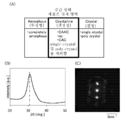
트랜지스터에 적용 가능한 반도체로서, 금속 산화물이 주목을 받고 있다. "IGZO", "이그조" 등이라고 불리는 In-Ga-Zn 산화물은 다원계 금속 산화물의 대표적인 것이다. IGZO에 관한 연구에서, 단결정도 비정질도 아닌, CAAC(c-axis aligned crystalline) 구조 및 nc(nanocrystalline) 구조가 발견되었다(예를 들어 비특허문헌 1).As a semiconductor applicable to transistors, metal oxides are attracting attention. In-Ga-Zn oxide called "IGZO" In the study about IGZO, neither single crystal nor amorphous, CAAC (c-axis aligned crystalline) structure and nc (nanocrystalline) structure were discovered (for example, nonpatent literature 1).
채널 형성 영역에 금속 산화물 반도체를 가지는 트랜지스터(이하, "산화물 반도체 트랜지스터" 또는 "OS 트랜지스터"라고 부르는 경우가 있음)는 오프 전류가 매우 작다는 것이 보고되어 있다(예를 들어 비특허문헌 1, 비특허문헌 2). OS 트랜지스터가 사용된 다양한 반도체 장치가 제작되어 있다(예를 들어, 비특허문헌 3, 비특허문헌 4).It has been reported that a transistor having a metal oxide semiconductor in the channel formation region (hereinafter, sometimes referred to as an "oxide semiconductor transistor" or an "OS transistor") has an extremely small off current (for example, Non-Patent
OS 트랜지스터의 제조 프로세스는 종래의 Si 트랜지스터의 CMOS 프로세스에 포함시킬 수 있고, OS 트랜지스터는 Si 트랜지스터 위에 적층하는 것이 가능하다. 예를 들어 특허문헌 1에서는 OS 트랜지스터를 가진 메모리 셀 어레이의 층을 Si 트랜지스터가 제공된 기판 위에 복수로 적층한 구성에 대하여 개시(開示)되어 있다.The manufacturing process of the OS transistor can be incorporated into the conventional CMOS process of the Si transistor, and the OS transistor can be stacked on the Si transistor. For example,
본 발명의 일 형태는 신규 구성의 반도체 장치 등을 제공하는 것을 과제 중 하나로 한다. 또는 본 발명의 일 형태는 극소한 오프 전류를 이용한 기억 장치로서 기능하는 반도체 장치에 있어서, 제조 비용의 저감을 도모할 수 있는 신규 구성의 반도체 장치 등을 제공하는 것을 과제 중 하나로 한다. 또는 본 발명의 일 형태는 극소한 오프 전류를 이용한 기억 장치로서 기능하는 반도체 장치에 있어서, 저소비 전력화에 뛰어난 신규 구성의 반도체 장치 등을 제공하는 것을 과제 중 하나로 한다. 또는 본 발명의 일 형태는 극소한 오프 전류를 이용한 기억 장치로서 기능하는 반도체 장치에 있어서, 장치의 소형화를 도모할 수 있는 신규 구성의 반도체 장치 등을 제공하는 것을 과제 중 하나로 한다. 또는 본 발명의 일 형태는 극소한 오프 전류를 이용한 기억 장치로서 기능하는 반도체 장치에 있어서, 트랜지스터의 전기 특성의 변동이 작고 신뢰성이 우수한 신규 구성의 반도체 장치 등을 제공하는 것을 과제 중 하나로 한다.One of the problems is to provide a semiconductor device or the like having a novel configuration. Another object of one embodiment of the present invention is to provide a semiconductor device or the like having a novel configuration capable of reducing manufacturing cost in a semiconductor device functioning as a memory device using a minimal off-state current. Another object of one embodiment of the present invention is to provide a semiconductor device having a novel configuration excellent in reducing power consumption in a semiconductor device functioning as a memory device using a minimal off-state current. Another object of one embodiment of the present invention is to provide a semiconductor device or the like of a novel configuration capable of reducing the size of a semiconductor device functioning as a memory device using a minimal off-state current. Another object of one aspect of the present invention is to provide a semiconductor device or the like of a novel configuration that has a small variation in the electrical characteristics of a transistor and is excellent in reliability in a semiconductor device functioning as a memory device using a minimal off-state current.
복수의 과제의 기재는 서로의 과제의 존재를 방해하는 것이 아니다. 본 발명의 일 형태는 예시한 과제를 모두 해결할 필요는 없다. 또한 열거한 것 외의 과제가 본 명세서의 기재로부터 저절로 명백해지고, 이러한 과제들도 본 발명의 일 형태의 과제가 될 수 있다.The description of a plurality of tasks does not prevent the existence of each other's tasks. One embodiment of the present invention does not need to solve all the exemplified problems. In addition, subjects other than those listed will become apparent by themselves from the description of the present specification, and these subjects may also become subjects of one embodiment of the present invention.
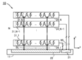
본 발명의 일 형태는 제 1 메모리 셀을 가지는 제 1 소자층과, 제 2 메모리 셀을 가지는 제 2 소자층과, 전환 회로를 가지는 제 3 소자층과, 구동 회로를 가지는 실리콘 기판을 가지고, 제 1 소자층은 실리콘 기판과 제 2 소자층 사이에 제공되고, 제 3 소자층은 실리콘 기판과 제 1 소자층 사이에 제공되고, 제 1 메모리 셀은 제 1 트랜지스터와 제 1 커패시터를 가지고, 제 2 메모리 셀은 제 2 트랜지스터와 제 2 커패시터를 가지고, 전환 회로는 제 1 메모리 셀 또는 제 2 메모리 셀과 구동 회로 사이의 도통 상태를 제어하는 기능을 가지는 제 3 트랜지스터를 가지고, 제 1 트랜지스터의 소스 및 드레인 중 한쪽 및 제 2 트랜지스터의 소스 및 드레인 중 한쪽은 각각 제 3 트랜지스터의 소스 및 드레인 중 한쪽에 전기적으로 접속하기 위한 배선에 전기적으로 접속되고, 제 3 트랜지스터의 소스 및 드레인 중 다른 쪽은 구동 회로에 전기적으로 접속되고, 배선은 제 1 트랜지스터가 가지는 제 1 반도체층 및 제 2 트랜지스터가 가지는 제 2 반도체층에 접하며 실리콘 기판의 표면에 대하여 수직 방향 또는 실질적으로 수직인 방향으로 제공되는, 반도체 장치이다.One aspect of the present invention includes a silicon substrate having a first element layer having a first memory cell, a second element layer having a second memory cell, a third element layer having a switching circuit, and a driving circuit, A first device layer is provided between the silicon substrate and the second device layer, a third device layer is provided between the silicon substrate and the first device layer, the first memory cell having a first transistor and a first capacitor, The memory cell has a second transistor and a second capacitor, and the switching circuit has a third transistor having a function of controlling a conduction state between the first memory cell or the second memory cell and the driving circuit, the source of the first transistor and One of the drains and one of the source and drain of the second transistor are electrically connected to a wiring for electrically connecting to one of the source and drain of the third transistor, respectively, and the other of the source and drain of the third transistor is a driving circuit is electrically connected to, and the wiring is provided in a direction perpendicular or substantially perpendicular to the surface of the silicon substrate in contact with the first semiconductor layer of the first transistor and the second semiconductor layer of the second transistor. .
본 발명의 일 형태에 있어서, 제 1 반도체층 및 제 2 반도체층은 각각 채널 형성 영역에 금속 산화물을 가지는 반도체 장치가 바람직하다.In one embodiment of the present invention, it is preferable that the first semiconductor layer and the second semiconductor layer each have a metal oxide in the channel formation region.
본 발명의 일 형태에 있어서, 제 1 커패시터는 제 1 반도체층의 아래층에 제공되고, 제 2 커패시터는 제 2 반도체층의 아래층에 제공되는 반도체 장치가 바람직하다.In one aspect of the present invention, it is preferable that the first capacitor is provided under the first semiconductor layer and the second capacitor is provided under the second semiconductor layer.
본 발명의 일 형태에 있어서, 제 1 커패시터는 제 1 반도체층의 위층에 제공되고, 제 2 커패시터는 제 2 반도체층의 위층에 제공되는 반도체 장치가 바람직하다.In one aspect of the present invention, it is preferable that the first capacitor is provided on an upper layer of the first semiconductor layer, and the second capacitor is provided on the upper layer of the second semiconductor layer.
본 발명의 일 형태에 있어서, 제 1 커패시터의 한쪽 전극은 제 1 반도체층과 같은 층에 제공되고, 제 2 커패시터의 한쪽 전극은 제 2 반도체층과 같은 층에 제공되는 반도체 장치가 바람직하다.In one embodiment of the present invention, it is preferable that one electrode of the first capacitor is provided on the same layer as the first semiconductor layer, and one electrode of the second capacitor is provided on the same layer as the second semiconductor layer.
본 발명의 일 형태는 제 1 메모리 셀을 가지는 제 1 소자층과, 제 2 메모리 셀을 가지는 제 2 소자층과, 제 1 제어 회로를 가지는 제 3 소자층과, 구동 회로를 가지는 실리콘 기판을 가지고, 상기 제 1 소자층은 상기 실리콘 기판과 상기 제 2 소자층 사이에 제공되고, 상기 제 3 소자층은 상기 실리콘 기판과 상기 제 1 소자층 사이에 제공되고, 상기 제 1 메모리 셀은 제 1 트랜지스터와 제 1 커패시터를 가지고, 상기 제 2 메모리 셀은 제 2 트랜지스터와 제 2 커패시터를 가지고, 상기 제 1 제어 회로는 상기 제 1 메모리 셀로부터 판독되는 신호를 증폭하기 위한 제 3 트랜지스터를 가지고, 제 1 트랜지스터의 소스 및 드레인 중 한쪽 및 제 2 트랜지스터의 소스 및 드레인 중 한쪽은 각각 상기 제 3 트랜지스터의 게이트에 전기적으로 하기 위한 제 1 배선에 전기적으로 접속되고, 제 3 트랜지스터의 소스 및 드레인 중 한쪽은 상기 구동 회로에 전기적으로 하기 위한 제 2 배선에 전기적으로 접속되고, 상기 제 1 배선은 상기 제 1 트랜지스터가 가지는 제 1 반도체층 및 상기 제 2 트랜지스터가 가지는 제 2 반도체층에 접하며 상기 실리콘 기판의 표면에 대하여 수직 방향 또는 실질적으로 수직인 방향으로 제공되고, 상기 제 2 배선은 상기 제 1 배선에 대하여 평행한 방향 또는 실질적으로 평행한 방향으로 제공되는 반도체 장치이다.One embodiment of the present invention includes a first element layer having a first memory cell, a second element layer having a second memory cell, a third element layer having a first control circuit, and a silicon substrate having a driving circuit, , the first device layer is provided between the silicon substrate and the second device layer, the third device layer is provided between the silicon substrate and the first device layer, and the first memory cell is a first transistor and a first capacitor, wherein the second memory cell has a second transistor and a second capacitor, and the first control circuit has a third transistor for amplifying a signal read from the first memory cell; One of the source and drain of the transistor and one of the source and drain of the second transistor are respectively electrically connected to the first wiring for electrically connecting the gate of the third transistor, and one of the source and drain of the third transistor is connected to the above It is electrically connected to a second wiring for electrically connecting to the driving circuit, and the first wiring is in contact with the first semiconductor layer of the first transistor and the second semiconductor layer of the second transistor, and is formed on the surface of the silicon substrate. The semiconductor device is provided in a direction perpendicular or substantially perpendicular to the semiconductor device, and the second wiring is provided in a direction parallel or substantially parallel to the first wiring.
본 발명의 일 형태에 있어서, 상기 제 1 제어 회로는 제 4 트랜지스터를 가지고, 상기 제 4 트랜지스터의 소스 및 드레인 중 한쪽은 상기 제 3 트랜지스터의 소스 및 드레인 중 한쪽에 전기적으로 접속되고, 상기 제 4 트랜지스터의 소스 및 드레인 중 다른 쪽은 상기 제 2 배선에 전기적으로 접속되는 반도체 장치가 바람직하다.In one aspect of the present invention, the first control circuit has a fourth transistor, one of a source and a drain of the fourth transistor is electrically connected to one of a source and a drain of the third transistor, Preferably, a semiconductor device in which the other of the source and drain of the transistor is electrically connected to the second wiring.
본 발명의 일 형태에 있어서, 상기 제 1 제어 회로는 제 5 트랜지스터 및 제 6 트랜지스터를 가지고, 상기 제 5 트랜지스터의 소스 및 드레인 중 한쪽은 상기 제 3 트랜지스터의 게이트에 전기적으로 접속되고, 상기 제 5 트랜지스터의 소스 및 드레인 중 다른 쪽은 상기 제 2 배선에 전기적으로 접속되고, 상기 제 6 트랜지스터의 소스 및 드레인 중 한쪽은 상기 제 3 트랜지스터의 소스 및 드레인 중 다른 쪽에 전기적으로 접속되고, 상기 제 6 트랜지스터의 소스 및 드레인 중 다른 쪽은 그라운드선에 전기적으로 접속되는 반도체 장치가 바람직하다.In one aspect of the present invention, the first control circuit includes a fifth transistor and a sixth transistor, and one of a source and a drain of the fifth transistor is electrically connected to a gate of the third transistor, and the fifth transistor The other of the source and the drain of the transistor is electrically connected to the second wiring, and one of the source and the drain of the sixth transistor is electrically connected to the other of the source and the drain of the third transistor, the sixth transistor It is preferable that the other of the source and the drain of the semiconductor device is electrically connected to the ground line.
본 발명의 일 형태에 있어서, 상기 제 1 반도체층 및 제 2 반도체층은 각각 채널 형성 영역에 금속 산화물을 가지는 반도체 장치가 바람직하다.In one embodiment of the present invention, it is preferable that the first semiconductor layer and the second semiconductor layer each have a metal oxide in a channel formation region.
본 발명의 일 형태에 있어서, 상기 금속 산화물은 In과, Ga과, Zn을 포함하는 반도체 장치가 바람직하다.In one embodiment of the present invention, the metal oxide is preferably a semiconductor device containing In, Ga, and Zn.
본 발명의 일 형태에 있어서, 상기 제 1 커패시터는 상기 제 1 반도체층의 아래층에 제공되고, 상기 제 2 커패시터는 상기 제 2 반도체층의 아래층에 제공되는 반도체 장치가 바람직하다.In one aspect of the present invention, it is preferable that the first capacitor is provided under the first semiconductor layer, and the second capacitor is provided under the second semiconductor layer.
본 발명의 일 형태에 있어서, 상기 제 1 커패시터는 상기 제 1 반도체층의 위층에 제공되고, 상기 제 2 커패시터는 상기 제 2 반도체층의 위층에 제공되는 반도체 장치가 바람직하다.In one aspect of the present invention, it is preferable that the first capacitor is provided on an upper layer of the first semiconductor layer, and the second capacitor is provided on an upper layer of the second semiconductor layer.
본 발명의 일 형태에 있어서, 상기 제 1 커패시터의 한쪽 전극은 상기 제 1 반도체층과 같은 층에 제공되고, 상기 제 2 커패시터의 한쪽 전극은 상기 제 2 반도체층과 같은 층에 제공되는 반도체 장치가 바람직하다.In one aspect of the present invention, there is provided a semiconductor device in which one electrode of the first capacitor is provided on the same layer as the first semiconductor layer, and one electrode of the second capacitor is provided on the same layer as the second semiconductor layer. desirable.
본 발명의 일 형태는 제 1 메모리 셀을 가지는 제 1 소자층과, 제 2 메모리 셀을 가지는 제 2 소자층을 가지고, 상기 제 1 소자층과 상기 제 2 소자층은 적층되어 제공되고, 상기 제 1 메모리 셀은 제 1 트랜지스터와 제 1 커패시터를 가지고, 상기 제 2 메모리 셀은 제 2 트랜지스터와, 제 3 트랜지스터와, 제 2 커패시터를 가지고, 상기 제 1 트랜지스터의 소스 및 드레인 중 한쪽은 상기 제 1 커패시터의 한쪽 전극에 전기적으로 접속되고, 상기 제 2 트랜지스터의 소스 및 드레인 중 한쪽은 상기 제 3 트랜지스터의 게이트 및 상기 제 2 커패시터의 한쪽 전극에 전기적으로 접속되는 반도체 장치이다.One aspect of the present invention is provided with a first element layer having a first memory cell and a second element layer having a second memory cell, wherein the first element layer and the second element layer are stacked, A first memory cell has a first transistor and a first capacitor, the second memory cell has a second transistor, a third transistor, and a second capacitor, and one of a source and a drain of the first transistor is the first A semiconductor device electrically connected to one electrode of a capacitor, and one of a source and a drain of the second transistor is electrically connected to a gate of the third transistor and one electrode of the second capacitor.
본 발명의 일 형태에 있어서, 기판을 가지고, 상기 제 2 소자층은 상기 기판과 상기 제 1 소자층 사이에 제공되는 반도체 장치가 바람직하다.In one aspect of the present invention, it is preferable that the semiconductor device has a substrate, wherein the second element layer is provided between the substrate and the first element layer.
본 발명의 일 형태에 있어서, 상기 제 1 트랜지스터는 제 1 반도체층을 가지고, 상기 제 2 트랜지스터는 제 2 반도체층을 가지고, 상기 제 1 반도체층 및 제 2 반도체층은 각각 채널 형성 영역에 금속 산화물을 가지는 반도체 장치가 바람직하다.In one embodiment of the present invention, the first transistor has a first semiconductor layer, the second transistor has a second semiconductor layer, and the first semiconductor layer and the second semiconductor layer each have a metal oxide in a channel formation region. A semiconductor device having a
본 발명의 일 형태에 있어서, 상기 금속 산화물은 In과, Ga과, Zn을 포함하는 반도체 장치가 바람직하다.In one embodiment of the present invention, the metal oxide is preferably a semiconductor device containing In, Ga, and Zn.
또한 상기 외의 본 발명의 일 형태에 대해서는 이하의 실시형태에서의 설명, 및 도면에 기재되어 있다.In addition, about one aspect of this invention other than the above, it describes in the description and drawings in the following embodiment.
본 발명의 일 형태는 신규 구성의 반도체 장치 등을 제공할 수 있다. 또는 본 발명의 일 형태는 극소한 오프 전류를 이용한 기억 장치로서 기능하는 반도체 장치에 있어서, 제조 비용의 저감을 도모할 수 있는 신규 구성의 반도체 장치 등을 제공할 수 있다. 또는 본 발명의 일 형태는 극소한 오프 전류를 이용한 기억 장치로서 기능하는 반도체 장치에 있어서, 저소비 전력성에 뛰어난 신규 구성의 반도체 장치 등을 제공할 수 있다. 또는 본 발명의 일 형태는 극소한 오프 전류를 이용한 기억 장치로서 기능하는 반도체 장치에 있어서, 장치의 소형화를 도모할 수 있는 신규 구성의 반도체 장치 등을 제공할 수 있다. 또는 본 발명의 일 형태는 극소한 오프 전류를 이용한 기억 장치로서 기능하는 반도체 장치에 있어서, 트랜지스터의 전기 특성의 변동이 작고 신뢰성이 우수한 신규 구성의 반도체 장치 등을 제공할 수 있다.One embodiment of the present invention can provide a semiconductor device or the like having a novel configuration. Alternatively, one embodiment of the present invention can provide a semiconductor device having a novel configuration capable of reducing manufacturing cost in a semiconductor device functioning as a memory device using a minimal off-state current. Alternatively, one embodiment of the present invention can provide a semiconductor device having a novel configuration excellent in low power consumption in a semiconductor device functioning as a memory device using a minimal off-state current. Alternatively, one embodiment of the present invention can provide a semiconductor device having a novel configuration capable of reducing the size of a semiconductor device functioning as a storage device using a minimal off-state current. Alternatively, one embodiment of the present invention can provide a semiconductor device having a novel configuration in which variations in electrical characteristics of transistors are small and reliability is excellent in a semiconductor device functioning as a memory device using a minimal off-state current.
복수의 효과의 기재는 다른 효과의 존재를 방해하는 것은 아니다. 또한 본 발명의 일 형태는 예시한 효과 모두를 반드시 가질 필요는 없다. 또한 본 발명의 일 형태에서, 상기 외의 과제, 효과, 및 신규 특징에 대해서는 본 명세서의 기재 및 도면으로부터 저절로 명백해진다.The description of a plurality of effects does not prevent the existence of other effects. In addition, one embodiment of the present invention does not necessarily have all of the illustrated effects. Moreover, in one aspect of this invention, about the subject other than the above, an effect, and a novel characteristic, it becomes clear from description and drawing of this specification spontaneously.
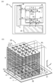
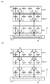
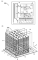
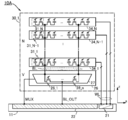
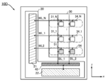
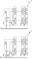
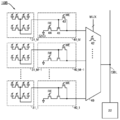
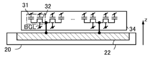
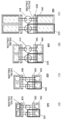
도 1은 반도체 장치의 구성예를 나타낸 (A) 블록도 및 (B) 모식도이다.
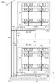
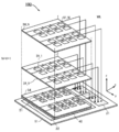
도 2는 반도체 장치의 구성예를 나타낸 모식도이다.
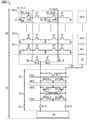
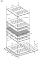
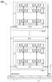
도 3은 반도체 장치의 구성예를 나타낸 (A) 모식도 및 (B) 모식도이다.
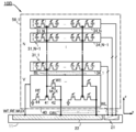
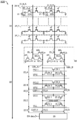
도 4는 반도체 장치의 구성예를 나타낸 회로도이다.
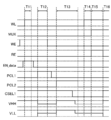
도 5는 반도체 장치의 구성예를 나타낸 타이밍 차트이다.
도 6은 반도체 장치의 구성예를 나타낸 (A) 블록도 및 (B) 모식도이다.
도 7은 반도체 장치의 구성예를 나타낸 모식도이다.
도 8은 반도체 장치의 구성예를 나타낸 회로도이다.
도 9는 반도체 장치의 구성예를 나타낸 모식도이다.
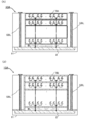
도 10은 반도체 장치의 구성예를 나타낸 (A) 모식도 및 (B) 모식도이다.
도 11은 반도체 장치의 구성예를 나타낸 (A) 블록도 및 (B) 모식도이다.
도 12는 반도체 장치의 구성예를 나타낸 (A) 블록도 및 (B) 회로도이다.
도 13은 반도체 장치의 구성예를 나타낸 블록도이다.
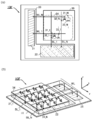
도 14는 반도체 장치의 구성예를 나타낸 모식도이다.
도 15는 반도체 장치의 구성예를 나타낸 모식도이다.
도 16은 반도체 장치의 구성예를 나타낸 모식도이다.
도 17은 반도체 장치의 구성예를 나타낸 모식도이다.
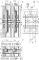
도 18은 반도체 장치의 구성예를 나타낸 (A) 회로도 및 (B) 회로도이다.
도 19는 반도체 장치의 구성예를 나타낸 (A) 회로도 및 (B) 회로도이다.
도 20은 반도체 장치의 구성예를 나타낸 회로도이다.
도 21은 반도체 장치의 구성예를 나타낸 회로도이다.
도 22는 반도체 장치의 구성예를 나타낸 회로도이다.
도 23은 반도체 장치의 구성예를 나타낸 타이밍 차트이다.
도 24는 반도체 장치의 구성예를 나타낸 회로도이다.
도 25는 반도체 장치의 구성예를 나타낸 (A) 블록도 및 (B) 모식도이다.
도 26은 반도체 장치의 구성예를 나타낸 모식도이다.
도 27은 반도체 장치의 구성예를 나타낸 (A) 모식도 및 (B) 모식도이다.
도 28은 반도체 장치의 구성예를 나타낸 회로도이다.
도 29는 반도체 장치의 구성예를 나타낸 타이밍 차트이다.
도 30은 반도체 장치의 구성예를 설명하는 모식도이다.
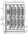
도 31은 반도체 장치의 구성예를 나타낸 모식도이다.
도 32는 반도체 장치의 구성예를 나타낸 모식도이다.
도 33은 반도체 장치의 구성예를 설명하는 모식도이다.
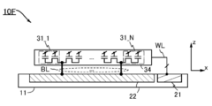
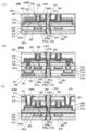
도 34는 반도체 장치의 구성예를 나타낸 단면 모식도이다.
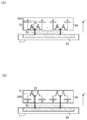
도 35는 반도체 장치의 구성예를 나타낸 (A) 단면 모식도 및 (B) 단면 모식도이다.
도 36은 반도체 장치의 구성예를 나타낸 (A) 단면 모식도, (B) 단면 모식도, 및 (C) 단면 모식도이다.
도 37은 반도체 장치의 구성예를 나타낸 단면 모식도이다.
도 38은 반도체 장치의 구성예를 나타낸 단면 모식도이다.
도 39는 반도체 장치의 구성예를 나타낸 (A) 상면도, (B) 단면 모식도, 및 (C) 단면 모식도이다.
도 40은 반도체 장치의 구성예를 나타낸 (A) 내지 (D) 상면도이다.
도 41은 (A) IGZO의 결정 구조의 분류를 설명하는 도면, (B) CAAC-IGZO막의 XRD 스펙트럼을 설명하는 도면, (C) CAAC-IGZO막의 극미 전자선 회절 패턴을 설명하는 도면이다.
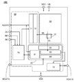
도 42는 반도체 장치의 구성예를 설명하는 블록도이다.
도 43은 반도체 장치의 구성예를 나타낸 개념도이다.
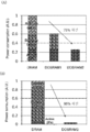
도 44는 반도체 장치의 구성예를 나타낸 (A) 그래프 및 (B) 그래프이다.
도 45는 전자 부품의 일례를 설명하는 (A) 모식도, (B) 모식도이다.
도 46은 전자 기기의 예를 나타낸 도면이다.BRIEF DESCRIPTION OF THE DRAWINGS It is (A) a block diagram and (B) a schematic diagram which showed the structural example of a semiconductor device.
2 is a schematic diagram showing a configuration example of a semiconductor device.
Fig. 3 is a schematic view (A) and a schematic view (B) showing a configuration example of a semiconductor device.
4 is a circuit diagram showing a configuration example of a semiconductor device.
5 is a timing chart showing a configuration example of a semiconductor device.
6 is a block diagram (A) and a schematic diagram (B) showing a configuration example of a semiconductor device.
7 is a schematic diagram showing a configuration example of a semiconductor device.
8 is a circuit diagram showing a configuration example of a semiconductor device.
9 is a schematic diagram showing a configuration example of a semiconductor device.
Fig. 10 is a schematic diagram (A) and a schematic diagram (B) showing a configuration example of a semiconductor device.
11 is a block diagram (A) and a schematic diagram (B) of a configuration example of a semiconductor device.
12 is a block diagram (A) and a circuit diagram (B) showing a configuration example of a semiconductor device.
13 is a block diagram showing a configuration example of a semiconductor device.
14 is a schematic diagram showing a configuration example of a semiconductor device.
15 is a schematic diagram showing a configuration example of a semiconductor device.
16 is a schematic diagram showing a configuration example of a semiconductor device.
17 is a schematic diagram showing a configuration example of a semiconductor device.
Fig. 18 is a circuit diagram (A) and a circuit diagram (B) showing a configuration example of a semiconductor device.
19 is (A) a circuit diagram and (B) a circuit diagram showing a configuration example of a semiconductor device.
20 is a circuit diagram showing a configuration example of a semiconductor device.
21 is a circuit diagram showing a configuration example of a semiconductor device.
22 is a circuit diagram showing a configuration example of a semiconductor device.
23 is a timing chart showing a configuration example of a semiconductor device.
24 is a circuit diagram showing a configuration example of a semiconductor device.
25 is a block diagram (A) and a schematic diagram (B) of a configuration example of a semiconductor device.
26 is a schematic diagram showing a configuration example of a semiconductor device.
Fig. 27 is a schematic view (A) and a schematic view (B) showing a configuration example of a semiconductor device.
28 is a circuit diagram showing a configuration example of a semiconductor device.
29 is a timing chart showing a configuration example of a semiconductor device.
It is a schematic diagram explaining the structural example of a semiconductor device.
31 is a schematic diagram showing a configuration example of a semiconductor device.
32 is a schematic diagram showing a configuration example of a semiconductor device.
33 is a schematic diagram for explaining a configuration example of a semiconductor device.
34 is a schematic cross-sectional view showing a configuration example of a semiconductor device.
Fig. 35 is a schematic cross-sectional view (A) and a schematic cross-sectional view (B) of a structural example of a semiconductor device.
Fig. 36 is (A) cross-sectional schematic view, (B) cross-sectional schematic view, and (C) cross-sectional schematic view showing a configuration example of a semiconductor device.
37 is a schematic cross-sectional view showing a configuration example of a semiconductor device.
38 is a schematic cross-sectional view showing a configuration example of a semiconductor device.
Fig. 39 is (A) a top view, (B) a schematic cross-sectional view, and (C) a cross-sectional schematic view showing a configuration example of a semiconductor device.
Fig. 40 is a top view (A) to (D) showing a configuration example of a semiconductor device.
FIG. 41 : (A) a figure explaining the classification of the crystal structure of IGZO, (B) a figure explaining the XRD spectrum of a CAAC-IGZO film, (C) a figure explaining the microelectron-beam diffraction pattern of a CAAC-IGZO film.
42 is a block diagram for explaining a configuration example of a semiconductor device.
43 is a conceptual diagram showing a configuration example of a semiconductor device.
44 is a graph (A) and a graph (B) showing a configuration example of a semiconductor device.
It is a schematic diagram (A) and (B) schematic diagram explaining an example of an electronic component.
46 is a diagram illustrating an example of an electronic device.
이하에서 본 발명의 실시형태에 대하여 설명한다. 다만, 본 발명의 일 형태는 이하의 설명에 한정되지 않고, 본 발명의 취지 및 그 범위에서 벗어남이 없이 그 형태 및 자세한 사항을 다양하게 변경할 수 있다는 것은 통상의 기술자라면 용이하게 이해된다. 따라서, 본 발명의 일 형태는 이하에 나타내는 실시형태의 기재 내용에 한정하여 해석되는 것이 아니다.EMBODIMENT OF THE INVENTION Below, embodiment of this invention is described. However, one embodiment of the present invention is not limited to the following description, and it is easily understood by those skilled in the art that various changes can be made in the form and details without departing from the spirit and scope of the present invention. Therefore, one embodiment of the present invention is not interpreted as being limited to the description of the embodiment shown below.
또한 본 명세서 등에서 '제 1', '제 2' 및 '제 3'이라는 서수사는 구성 요소의 혼동을 피하기 위하여 붙인 것이다. 따라서 구성 요소의 수를 한정하는 것은 아니다. 또한 구성 요소의 순서를 한정하는 것은 아니다. 또한 예를 들어 본 명세서 등의 한 실시형태에서 '제 1'이라고 언급된 구성 요소가 다른 실시형태 또는 청구범위에서 '제 2'라고 언급된 구성 요소가 될 수도 있다. 또한 예를 들어 본 명세서 등의 한 실시형태에서 '제 1'이라고 언급된 구성 요소를 다른 실시형태 또는 청구범위에서 생략할 수도 있다.Also, in this specification, ordinal numbers such as 'first', 'second', and 'third' are added to avoid confusion of components. Therefore, the number of components is not limited. Also, the order of the components is not limited. Also, for example, a component referred to as 'first' in one embodiment such as this specification may be a component referred to as 'second' in another embodiment or claim. Also, for example, a component referred to as 'first' in one embodiment such as this specification may be omitted from another embodiment or claims.
도면에서 동일한 요소 또는 같은 기능을 가지는 요소, 동일한 재질의 요소, 또는 동시에 형성되는 요소 등에는 동일한 부호를 붙이는 경우가 있고, 이의 반복적인 설명은 생략하는 경우가 있다.In the drawings, the same reference numerals may be attached to the same elements or elements having the same function, elements made of the same material, or elements formed at the same time, and repeated descriptions thereof may be omitted.
본 명세서에서 예를 들어 전원 전위(VDD)를 전위(VDD), VDD 등이라고 생략하여 기재하는 경우가 있다. 이는 다른 구성 요소(예를 들어 신호, 전압, 회로, 소자, 전극, 배선 등)에 대해서도 마찬가지이다.In this specification, for example, the power supply potential VDD may be omitted and described as the potential VDD, VDD, or the like. The same is true for other components (eg signals, voltages, circuits, devices, electrodes, wiring, etc.).
또한 복수의 요소에 같은 부호를 사용하는 경우, 특히 이들을 구별할 필요가 있을 때는 부호에 "_1", "_2", "[n]", "[m, n]" 등의 식별용 부호를 부기하여 기재하는 경우가 있다. 예를 들어 두 번째의 배선(GL)을 배선(GL[2])이라고 기재한다.In addition, when the same code is used for multiple elements, especially when it is necessary to distinguish them, an identification code such as "_1", "_2", "[n]", "[m, n]" is added to the code It is sometimes described. For example, the second wiring GL is described as a wiring GL[2].
(실시형태 1)(Embodiment 1)
본 발명의 일 형태인 반도체 장치 및 반도체 장치의 동작 방법의 구성예에 대하여, 도 1 내지 도 5를 참조하여 설명한다.A configuration example of a semiconductor device and a method of operating a semiconductor device according to one embodiment of the present invention will be described with reference to FIGS. 1 to 5 .
또한, 반도체 장치는 반도체 특성을 이용한 장치이며 반도체 소자(트랜지스터, 다이오드, 포토다이오드 등)를 포함하는 회로, 이 회로를 가지는 장치이다. 본 실시형태에서 설명하는 반도체 장치는 극소한 오프 전류의 트랜지스터를 이용한 기억 장치로서 기능하는 반도체 장치로서 기능시킬 수 있다.Further, a semiconductor device is a device using semiconductor characteristics, and is a circuit including a semiconductor element (transistor, diode, photodiode, etc.), and a device having this circuit. The semiconductor device described in this embodiment can function as a semiconductor device functioning as a memory device using a transistor with a minimal off-state current.
도 1의 (A)는 본 실시형태에서 설명하는 반도체 장치의 블록도이다. 도 1의 (A)에 도시된 반도체 장치(10)는 주변 회로(20) 및 메모리 셀 어레이(30)를 가진다.Fig. 1A is a block diagram of a semiconductor device described in this embodiment. The
주변 회로(20)는 행 드라이버(row driver)(21) 및 열 드라이버(column driver)(22)를 가진다. 행 드라이버(21) 및 열 드라이버(22)는 단순히 구동 회로 또는 드라이버라고 하는 경우가 있다.The
행 드라이버(21)는 워드선(WL)에 메모리 셀 어레이(30)를 구동하기 위한 신호를 출력하는 기능을 가지는 회로이다. 구체적으로 행 드라이버(21)는 워드선(WL)(도 1의 (A)에서는 WL_1 및 WL_N을 도시하였음. N은 2 이상의 자연수)에 워드 신호를 전달하는 기능을 가진다. 행 드라이버(21)는 워드선 측 구동 회로라고 하는 경우가 있다. 또한 행 드라이버(21)는 지정된 어드레스에 대응하는 워드선(WL)을 선택하기 위한 디코더 회로 및 버퍼 회로 등을 포함한다. 또한 워드선(WL)은 단순히 배선이라고 하는 경우가 있다.The
열 드라이버(22)는 비트선(BL)에 메모리 셀 어레이(30)를 구동하기 위한 신호를 출력하는 기능을 가지는 회로이다. 구체적으로 열 드라이버(22)는 비트선(BL)(도 1의 (A)에서는 BL_1 및 BL_2)에 데이터 신호를 전달하는 기능을 가진다. 열 드라이버(22)는 비트선 측 구동 회로라고 하는 경우가 있다. 또한 열 드라이버(22)는 감지 증폭기, 프리차지 회로, 지정된 어드레스에 대응하는 비트선을 선택하기 위한 디코더 회로 등을 포함한다. 또한 비트선(BL)은 단순히 배선이라고 하는 경우가 있다. 또한 도면에 있어서, 시인성을 높기 위하여 비트선(BL)은 굵은 선 또는 굵은 점선 등으로 도시되어 있는 경우가 있다.The
비트선(BL)에 공급되는 데이터 신호는 메모리 셀에 기록되는 신호, 또는 메모리 셀로부터 판독되는 신호에 상당한다. 데이터 신호는 데이터 1 또는 데이터 0에 대응하는 하이 레벨 또는 로(low) 레벨의 전위를 가지는 2개의 값의 신호로서 설명한다. 또한 데이터 신호는, 3개의 값 이상의 다치(多値)이어도 좋다. 하이 레벨의 전위는 VDD이고, 로 레벨의 전위는 VSS 또는 그라운드 전위(GND)이다. 비트선(BL)에 공급되는 신호로서는 데이터 신호 외에, 데이터를 판독하기 위한 프리차지 전위 등이 있다. 프리차지 전위는 VDD/2로 할 수 있다.The data signal supplied to the bit line BL corresponds to a signal written to the memory cell or a signal read out from the memory cell. A data signal is described as a two-valued signal having a potential of a high level or a low level corresponding to
메모리 셀 어레이(30)는 복수, 예를 들어 N층(N은 2 이상의 자연수)의 소자층(34_1 내지 34_N)을 가진다. 소자층(34_1)은 하나 이상의 메모리 셀(31_1)을 가진다. 메모리 셀(31_1)은 트랜지스터(32_1) 및 커패시터(33_1)를 가진다. 소자층(34_N)은 하나 이상의 메모리 셀(31_N)을 가진다. 메모리 셀(31_N)은 트랜지스터(32_N) 및 커패시터(33_N)를 가진다. 또한 커패시터는 용량 소자라고 부르는 경우가 있다. 또한 소자층은 커패시터나 트랜지스터 등의 소자가 제공되는 층이고, 도전체, 반도체, 절연체 등의 부재로 구성되는 층이다.The
트랜지스터(32_1 내지 32_N)는 워드선(WL_1 내지 WL_N)에 공급되는 워드 신호에 따라 온 또는 오프가 제어되는 스위치로서 기능한다. 트랜지스터(32_1 내지 32_N)는 각각 소스 및 드레인 중 한쪽이 비트선(BL) 중 어느 하나(도면 중, BL_1)에 접속된다.The transistors 32_1 to 32_N function as switches whose ON or OFF is controlled according to a word signal supplied to the word lines WL_1 to WL_N. Each of the transistors 32_1 to 32_N has one of a source and a drain connected to one of the bit lines BL (BL_1 in the drawing).
트랜지스터(32_1 내지 32_N)로서는, 채널 형성 영역이 산화물 반도체를 가지는 트랜지스터(이하, OS 트랜지스터라고 함)로 구성되는 것이 바람직하다. 본 발명의 일 형태의 구성에서는, OS 트랜지스터를 가지는 메모리 셀을 사용하는 구성으로 함으로써, 오프 시에 소스와 드레인 사이를 흐르는 누설 전류(이하, 오프 전류)가 매우 낮은 특성을 이용하여, 원하는 전압에 따른 전하를 소스 및 드레인 중 다른 쪽에 있는 커패시터(33_1 내지 33_N)에 유지시킬 수 있다. 즉 메모리 셀(31_1 내지 31_N)에, 한번 기록한 데이터를 장시간 유지시킬 수 있다. 그러므로, 데이터 리프레시의 빈도를 낮추고 저소비 전력화를 도모할 수 있다.As the transistors 32_1 to 32_N, it is preferable that the channel formation region is formed of a transistor having an oxide semiconductor (hereinafter referred to as an OS transistor). In the configuration of one embodiment of the present invention, by using a memory cell having an OS transistor, the leakage current flowing between the source and the drain (hereinafter, the off current) at the time of OFF is very low, so that a desired voltage is obtained. The corresponding charge may be maintained in the capacitors 33_1 to 33_N located on the other side of the source and the drain. That is, data written once can be maintained in the memory cells 31_1 to 31_N for a long time. Therefore, the frequency of data refresh can be reduced and power consumption can be reduced.
이에 더하여, OS 트랜지스터를 사용한 메모리 셀(31_1 내지 31_N)에서는 전하를 충전 또는 방전함으로써 데이터의 재기록 및 판독이 가능하게 되므로 데이터의 기록 및 판독 횟수를 실질적으로 무제한으로 할 수 있다. OS 트랜지스터를 사용한 메모리 셀(31_1 내지 31_N)는, 자기 메모리 또는 저항 변화형 메모리 등과 달리, 원자 레벨에서의 구조 변화가 일어나지 않으므로 재기록 내성이 뛰어나다. 또한 OS 트랜지스터를 사용한 메모리 셀(31_1 내지 31_N)은 플래시 메모리와 달리, 재기록 동작을 반복하여도 전자 포획 중심의 증가로 인한 불안정성이 확인되지 않는다.In addition, in the memory cells 31_1 to 31_N using OS transistors, since data can be rewritten and read by charging or discharging electric charges, the number of times of data writing and reading can be substantially unlimited. The memory cells 31_1 to 31_N using OS transistors, unlike magnetic memories or resistance-variable memories, do not undergo structural change at the atomic level, and thus have excellent rewrite resistance. Also, unlike the flash memory, in the memory cells 31_1 to 31_N using OS transistors, instability due to an increase in the electron trapping center is not confirmed even when the rewrite operation is repeated.
또한 OS 트랜지스터를 사용한 메모리 셀(31_1 내지 31_N)은 채널 형성 영역에 실리콘을 포함하는 트랜지스터(이하, Si 트랜지스터)를 가지는 실리콘 기판 위 등에 자유로이 배치할 수 있기 때문에 집적화가 용이하다. 또한 OS 트랜지스터는 Si 트랜지스터와 같은 제조 장치를 사용하여 제작할 수 있으므로 낮은 비용으로 제작할 수 있다.In addition, since the memory cells 31_1 to 31_N using OS transistors can be freely disposed on a silicon substrate or the like having a transistor including silicon (hereinafter referred to as a Si transistor) in the channel formation region, integration is easy. In addition, the OS transistor can be manufactured at a low cost because it can be manufactured using the same manufacturing device as the Si transistor.
또한 OS 트랜지스터는 게이트 전극, 소스 전극, 및 드레인 전극에 더하여 백 게이트 전극을 포함하면, 4단자의 반도체 소자로 할 수 있다. OS 트랜지스터는, 게이트 전극 또는 백 게이트 전극에 인가하는 전압에 따라, 소스와 드레인 사이를 흐르는 신호의 입출력을 독립적으로 제어할 수 있는 전기 회로망으로 구성할 수 있다. 그러므로 LSI와 같은 사상으로 회로 설계를 수행할 수 있다. 그리고 OS 트랜지스터는 고온 환경하에서 Si 트랜지스터보다 뛰어난 전기 특성을 가진다. 구체적으로는 125℃ 이상 150℃ 이하와 같은 높은 온도에서도 온 전류와 오프 전류의 비가 크기 때문에 양호한 스위칭 동작을 수행할 수 있다.In addition, if the OS transistor includes a back gate electrode in addition to a gate electrode, a source electrode, and a drain electrode, it can be set as a four-terminal semiconductor device. The OS transistor can be configured as an electric circuit that can independently control input/output of a signal flowing between a source and a drain according to a voltage applied to the gate electrode or the back gate electrode. Therefore, circuit design can be performed with the same idea as LSI. In addition, the OS transistor has superior electrical characteristics than the Si transistor under a high-temperature environment. Specifically, even at a high temperature such as 125°C or more and 150°C or less, a good switching operation can be performed because the ratio of the on-current to the off-current is large.
또한 도 1의 (A)에 나타낸 메모리 셀은 OS 트랜지스터가 메모리에 사용된 DOSRAM(Dynamic Oxide Semiconductor Random Access Memory)이라고 부를 수 있다. 하나의 트랜지스터 및 하나의 용량 소자로 구성할 수 있으므로 메모리의 고밀도화를 실현할 수 있다. 또한, OS 트랜지스터를 사용함으로써, 데이터의 유지 기간을 길게 할 수 있다. 커패시터(33_1 내지 33_N)는 전극이 되는 도전체 사이에 절연체가 개재(介在)된 구성이다. 또한 전극을 구성하는 도전체로서는, 금속 외에, 도전성을 부여한 반도체층 등을 사용할 수 있다. 또한 자세한 사항은 후술하지만, 커패시터(33_1 내지 33_N)를 트랜지스터(32_1 내지 32_N)의 위쪽 또는 아래쪽에서 중첩되는 위치에 배치할 뿐만 아니라 트랜지스터(32_1 내지 32_N)를 구성하는 반도체층 또는 전극 등의 일부를 커패시터(33_1 내지 33_N)의 한쪽 전극으로서 사용할 수 있다.Also, the memory cell shown in FIG. 1A can be called a DOSRAM (Dynamic Oxide Semiconductor Random Access Memory) in which an OS transistor is used for a memory. Since it can be configured with one transistor and one capacitor, it is possible to realize high density of the memory. In addition, by using the OS transistor, the data retention period can be lengthened. The capacitors 33_1 to 33_N have a configuration in which an insulator is interposed between conductors serving as electrodes. Moreover, as a conductor which comprises an electrode, the semiconductor layer etc. which provided electroconductivity other than a metal can be used. In addition, although the details will be described later, the capacitors 33_1 to 33_N are not only disposed at positions overlapping above or below the transistors 32_1 to 32_N, but also a part of the semiconductor layers or electrodes constituting the transistors 32_1 to 32_N. It can be used as one electrode of the capacitors 33_1 to 33_N.
도 1의 (A)에서 설명한 각 구성에 있어서, 본 발명의 일 형태에 포함되는 소자층(34_1 내지 34_N)에 대하여 설명하기 위하여, 도 1의 (B)에 나타낸 모식도를 사용하여 설명한다. 도 1의 (B)에 도시된 모식도는 도 1의 (A)에서 설명한 각 구성의 배치를 설명하기 위하여 x축, y축, z축 방향을 규정한 사시도에 대응한다. 또한 이해를 용이하게 하기 위하여, 명세서 중에서 x축 방향을 깊이 방향, y축 방향을 수평 방향, z축 방향을 수직 방향이라고 부르는 경우가 있다.In order to explain the element layers 34_1 to 34_N included in one embodiment of the present invention in each configuration described with reference to Fig. 1A, the schematic diagram shown in Fig. 1B is used. The schematic diagram shown in FIG. 1B corresponds to a perspective view in which the x-axis, y-axis, and z-axis directions are defined in order to explain the arrangement of each configuration described in FIG. 1A . Also, in order to facilitate understanding, in the specification, the x-axis direction is referred to as a depth direction, the y-axis direction is referred to as a horizontal direction, and the z-axis direction is sometimes referred to as a vertical direction.
도 1의 (B)에 도시된 바와 같이 소자층(34_1 내지 34_N)은 N층으로 적층되어 제공된다. 메모리 셀(31_1 내지 31_N)을 가지는 소자층(34_1 내지 34_N)은 각각 실리콘 기판(11)에 제공된 열 드라이버(22)와 중첩되는 영역을 가진다. 도 1의 (B)에 도시된 바와 같이 소자층(34_1)은 실리콘 기판(11)과 소자층(34_N) 사이에 제공된다고도 할 수 있다.As shown in FIG. 1B , the device layers 34_1 to 34_N are provided by being stacked in N layers. The device layers 34_1 to 34_N having the memory cells 31_1 to 31_N each have a region overlapping with the
또한 소자층(34_1)이 가지는 메모리 셀(31_1)의 트랜지스터와, 소자층(34_N)이 가지는 메모리 셀(31_N)의 트랜지스터는 수직 방향으로 제공된 비트선(BL)을 통하여 접속된다. 또한 비트선(BL)은 실리콘 기판(11)에 제공된 열 드라이버(22)에 접속된다.Also, the transistor of the memory cell 31_1 included in the device layer 34_1 and the transistor of the memory cell 31_N included in the device layer 34_N are connected through bit lines BL provided in the vertical direction. The bit line BL is also connected to the
비트선(BL_1)은 메모리 셀(31_1)이 가지는 트랜지스터의 반도체층 및 메모리 셀(31_N)이 가지는 트랜지스터의 반도체층과 접하여 제공된다. 또는 비트선(BL_1)은 메모리 셀(31_1)이 가지는 트랜지스터의 반도체층의 소스 또는 드레인으로서 기능하는 영역 및 메모리 셀(31_N)이 가지는 트랜지스터의 반도체층의 소스 또는 드레인으로서 기능하는 영역과 접하여 제공된다. 또는 비트선(BL_1)은 메모리 셀(31_1)이 가지는 트랜지스터의 반도체층의 소스 또는 드레인으로서 기능하는 영역과 접하여 제공되는 도전체 및 메모리 셀(31_N)이 가지는 트랜지스터의 반도체층의 소스 또는 드레인으로서 기능하는 영역과 접하여 제공되는 도전체와 접하여 제공된다. 즉 비트선(BL)은 메모리 셀(31_1)이 가지는 트랜지스터의 소스 및 드레인 중 한쪽과, 메모리 셀(31_N)이 가지는 트랜지스터의 소스 및 드레인 중 한쪽과, 열 드라이버(22)를 수직 방향으로 전기적으로 하기 위한 배선이라고 할 수 있다.The bit line BL_1 is provided in contact with the semiconductor layer of the transistor included in the memory cell 31_1 and the semiconductor layer of the transistor included in the memory cell 31_N. Alternatively, the bit line BL_1 is provided in contact with a region serving as a source or drain of the semiconductor layer of the transistor of the memory cell 31_1 and a region serving as a source or drain of the semiconductor layer of the transistor of the memory cell 31_N. . Alternatively, the bit line BL_1 serves as a conductor provided in contact with a region serving as a source or drain of the semiconductor layer of the transistor of the memory cell 31_1 and as a source or drain of the semiconductor layer of the transistor of the memory cell 31_N. It is provided in contact with the conductor provided in contact with the region to be used. That is, the bit line BL electrically connects one of the source and the drain of the transistor of the memory cell 31_1, one of the source and the drain of the transistor of the memory cell 31_N, and the
또한 비트선(BL)은 열 드라이버(22)가 제공되는 실리콘 기판(11)의 면에 대하여 수직 방향 또는 실질적으로 수직인 방향으로 연장되어 제공된다고 할 수 있다. 즉 도 1의 (B)에 도시된 바와 같이 비트선(BL)은 메모리 셀(31_1)이 가지는 트랜지스터 및 메모리 셀(31_N)이 가지는 트랜지스터에 접속되며 상기 실리콘 기판의 표면(xy 평면)에 대하여 수직 방향 또는 실질적으로 수직인 방향'(z방향)으로 제공된다. 또한 "실질적으로 수직"이란, 85° 이상 95° 이하의 각도로 배치되어 있는 상태를 말한다.In addition, it can be said that the bit line BL extends in a direction perpendicular or substantially perpendicular to the surface of the
또한 실리콘 기판(11)에 제공된 행 드라이버(21)와, 소자층(34_1) 내지 소자층(34_N)의 깊이 방향으로 연장되어 제공되는 워드선(WL)과는 소자층(34_1) 내지 소자층(34_N)의 메모리 셀(31_1 내지 31_N)이 제공되지 않는 영역, 예를 들어 소자층(34_1) 내지 소자층(34_N)의 외주부에서의 개구부를 통하여 접속되는 구성으로 하면 좋다. 실리콘 기판(11)에 제공된 행 드라이버(21)와 각 소자층에 제공된 워드선(WL)은 소자층(34_1) 내지 소자층(34_N)의 위층에 제공되는 배선을 통하여 접속되어도 좋다.In addition, the
본 발명의 일 형태는 각 소자층에 제공되는 트랜지스터로서, 오프 전류가 매우 낮은 OS 트랜지스터를 사용한다. 그러므로, 메모리 셀에 유지되는 데이터의 리프레시 빈도를 저감할 수 있어, 저소비 전력화가 도모된 반도체 장치로 할 수 있다. OS 트랜지스터는 적층하여 제공할 수 있고, 수직 방향으로 반복적으로 같은 제조 공정을 사용하여 제작할 수 있어, 제조 비용의 저감을 도모할 수 있다. 또한 본 발명의 일 형태는, 메모리 셀을 구성하는 트랜지스터를 평면 방향이 아니라 수직 방향으로 배치함으로써, 메모리 밀도의 향상을 도모할 수 있어, 장치의 소형화를 도모할 수 있다. 또한, OS 트랜지스터는 고온 환경하에서도 Si 트랜지스터에 비하여 전기 특성의 변동이 작으므로, 적층하며 집적화할 때의 트랜지스터의 전기 특성의 변동이 작고 신뢰성이 우수한 기억 장치로서 기능하는 반도체 장치로 할 수 있다. 또한 본 발명의 일 형태는, 메모리 셀 어레이로부터 연장되어 제공되는 비트선을 수직 방향으로 제공함으로써, 메모리 셀 어레이와 열 드라이버의 비트선의 길이를 짧게 할 수 있다. 그러므로, 비트선의 기생 용량을 크게 삭감할 수 있어, 메모리 셀에 유지되는 데이터 신호를 다치화하여도 전위를 판독할 수 있다.In one embodiment of the present invention, an OS transistor having a very low off-state current is used as a transistor provided in each element layer. Therefore, it is possible to reduce the refresh frequency of data held in the memory cell, and a semiconductor device with reduced power consumption can be achieved. OS transistors can be provided by stacking, and can be manufactured using the same manufacturing process repeatedly in the vertical direction, thereby reducing manufacturing cost. In one embodiment of the present invention, by arranging the transistors constituting the memory cell in the vertical direction instead of in the planar direction, the memory density can be improved and the device can be downsized. In addition, since the OS transistor has less variation in electrical characteristics compared to the Si transistor even under a high-temperature environment, it can be used as a semiconductor device functioning as a reliable memory device with small variation in the electrical characteristics of the transistors when stacked and integrated. Further, according to one embodiment of the present invention, the length of the bit lines of the memory cell array and the column driver can be shortened by providing the bit lines extended from the memory cell array in the vertical direction. Therefore, the parasitic capacitance of the bit line can be greatly reduced, and the potential can be read even when the data signal held in the memory cell is multi-valued.
도 2에서는, 도 1의 (A) 및 (B)를 사용하여 설명한 반도체 장치(10)의 수직 방향(z축 방향)에 평행한 면의 단면 모식도에 대하여 나타내었다.In FIG. 2, the cross-sectional schematic diagram of the plane parallel to the perpendicular|vertical direction (z-axis direction) of the
도 2에 도시된 바와 같이 반도체 장치(10)는 각 층의 소자층에 제공된 메모리 셀(31_1 내지 31_N)과, 실리콘 기판(11)에 제공되는 열 드라이버(22)를 최단 거리인 수직 방향으로 제공되는 비트선(BL)을 통하여 접속하는 구성으로 할 수 있다. 비트선(BL)을 평면 방향으로 배치하는 구성에 비하여 비트선(BL)의 개수는 증가되지만 하나의 비트선에 접속되는 메모리 셀(31_1 내지 31_N)의 개수를 줄일 수 있기 때문에 비트선(BL)의 기생 용량을 작게 할 수 있다. 그러므로, 메모리 셀(31_1 내지 31_N)이 가지는 커패시터(33_1 내지 33_N)의 용량을 작게 하여도 전하의 이동에 따른 비트선(BL)의 전위를 변동시킬 수 있다.As shown in FIG. 2 , the
또한 메모리 셀(31_1 내지 31_N)이 가지는 커패시터(33_1 내지 33_N)의 용량을 작게 할 수 있으므로, 커패시터(33_1 내지 33_N)를 트랜지스터(32_1 내지 32_N)와 같은 층에 제공할 수 있다. 커패시터(33_1 내지 33_N)를 트랜지스터(32_1 내지 32_N)와 같은 층에 제공하는 구성으로 함으로써, 각 소자층(34_1 내지 34_N)을 얇게 할 수 있다. 그러므로, 반도체 장치(10)의 소형화를 도모할 수 있다.In addition, since the capacitance of the capacitors 33_1 to 33_N of the memory cells 31_1 to 31_N can be reduced, the capacitors 33_1 to 33_N can be provided on the same layer as the transistors 32_1 to 32_N. By providing the capacitors 33_1 to 33_N on the same layer as the transistors 32_1 to 32_N, each of the device layers 34_1 to 34_N can be made thin. Therefore, the size of the
또한 메모리 셀(31_1 내지 31_N)이 가지는 커패시터(33_1 내지 33_N)는 트랜지스터(32_1 내지 32_N)와 같은 층에 제공하는 구성이어도 좋지만, 다른 구성이어도 좋다. 예를 들어, 도 3의 (A)에 나타낸 모식도에서는, 소자층(34_1 내지 34_N)이 가지는 메모리 셀(31)의 커패시터(33A)가 트랜지스터(32)에 대하여 수직 방향으로 위쪽에 제공되는 구성을 나타내었다. 상기 구성으로 함으로써 용량을 크게 할 수 있기 때문에 판독되는 데이터의 신뢰성, 데이터의 유지 시간의 향상을 도모할 수 있다. 이에 더하여, 도 3의 (A)의 구성에서는 한쪽 전극이 고정 전위에 접속된 커패시터(33A)의 전극을 트랜지스터(32)의 위쪽에 배치할 수 있기 때문에 외부로부터의 노이즈의 영향을 억제할 수 있다.The capacitors 33_1 to 33_N included in the memory cells 31_1 to 31_N may be provided in the same layer as the transistors 32_1 to 32_N, but may have a different configuration. For example, in the schematic diagram shown in FIG. 3A , the
또한 도 3의 (B)에 나타낸 모식도에서는 소자층(34_1 내지 34_N)이 가지는 메모리 셀(31)의 커패시터(33B)가 트랜지스터(32)에 대하여 수직 방향으로 아래쪽에 제공되는 구성을 나타내었다. 상기 구성으로 함으로써 용량을 크게 할 수 있기 때문에 판독되는 데이터의 신뢰성, 데이터의 유지 시간의 향상을 도모할 수 있다. 이에 더하여 도 3의 (B)의 구성에서는 한쪽 전극이 고정 전위에 접속된 커패시터(33B)의 전극을 트랜지스터(32)와 열 드라이버(22) 사이에 배치할 수 있기 때문에 열 드라이버(22)의 노이즈가 메모리 셀(31)에 영향을 미치는 것을 억제할 수 있다.Also, in the schematic diagram shown in FIG. 3B , the
도 4는 도 1의 (A)에서 설명한, 소자층(34_1 내지 34_N)을 가지는 메모리 셀 어레이(30)의 회로의 구성예와, 상기 메모리 셀에 접속되는 열 드라이버(22)의 구체적인 회로의 구성예에 대하여 설명하는 회로도이다.4 is an example of the circuit configuration of the
도 4에는 메모리 셀 어레이(30)로서 소자층(34_1 내지 34_N)을 도시하였다. 도 4에서는 비트선(BL_A)에 접속된 메모리 셀로서 메모리 셀(31_N_A)을 도시하였다. 메모리 셀(31_N_A)은 게이트가 워드선(WL_A)에 접속된 트랜지스터(32A)와 커패시터(33)를 가진다. 또한 도 4에서는 비트선(BL_B)에 접속된 메모리 셀로서 메모리 셀(31_N_B)을 도시하였다. 메모리 셀(31_N_B)은 게이트가 워드선(WL_B)에 접속된 트랜지스터(32B)와 커패시터(33)를 가진다. 각 소자층의 커패시터(33)는 고정 전위, 예를 들어 그라운드 전위가 공급되는 배선(VL)에 접속된다.4 illustrates the device layers 34_1 to 34_N as the
또한 도 4에는 열 드라이버(22)가 가지는 회로로서, 실리콘 기판 측에 있는 프리차지 회로(22_1), 감지 증폭기(22_2), 선택 스위치(22_3), 기록 판독 회로(29)를 나타내었다. 프리차지 회로(22_1) 및 감지 증폭기(22_2)를 구성하는 트랜지스터로서, Si 트랜지스터를 사용한다. 선택 스위치(22_3)에도 Si 트랜지스터를 사용할 수 있다.4 shows a precharge circuit 22_1 , a sense amplifier 22_2 , a select switch 22_3 , and a write/
프리차지 회로(22_1)는 n채널형 트랜지스터(24_1 내지 24_3)로 구성된다. 프리차지 회로(22_1)는 프리차지선(PCL)에 공급되는 프리차지 신호에 따라, 비트선(BL_A) 및 비트선(BL_B)을 VDD와 VSS의 중간의 전위 VDD/2에 상당하는 중간 전위 VPC로 프리차지하기 위한 회로이다.The precharge circuit 22_1 includes n-channel transistors 24_1 to 24_3. In response to the precharge signal supplied to the precharge line PCL, the precharge circuit 22_1 connects the bit lines BL_A and the bit lines BL_B to an intermediate potential VPC corresponding to an intermediate potential VDD/2 between VDD and VSS. It is a circuit for precharging with
감지 증폭기(22_2)는 배선(VHH) 또는 배선(VLL)에 접속된, p채널형 트랜지스터(25_1, 25_2) 및 n채널형 트랜지스터(25_3, 25_4)로 구성된다. 배선(VHH) 또는 배선(VLL)은 VDD 또는 VSS를 공급하는 기능을 가지는 배선이다. 트랜지스터(25_1 내지 25_4)는 인버터 루프를 구성하는 트랜지스터이다. 감지 증폭기(22_2)는 워드선(WL_A, WL_B)을 하이 레벨로 하고 메모리 셀(31_N_A, 31_N_B)을 선택함으로써 변화하는 비트선(BL_A) 및 비트선(BL_B)의 전위를 고전원 전위 VDD 또는 저전원 전위 VSS로 한다. 비트선(BL_A) 및 비트선(BL_B)의 전위는 기록 판독 회로(29)를 통하여 외부에 출력할 수 있다. 비트선(BL_A) 및 비트선(BL_B)은 비트선쌍에 상당한다.The sense amplifier 22_2 includes p-channel transistors 25_1 and 25_2 and n-channel transistors 25_3 and 25_4 connected to the wiring VHH or VLL. The wiring VHH or the wiring VLL is a wiring having a function of supplying VDD or VSS. Transistors 25_1 to 25_4 are transistors constituting an inverter loop. The sense amplifier 22_2 sets the word lines WL_A and WL_B to a high level and selects the memory cells 31_N_A and 31_N_B to change the potentials of the bit lines BL_A and BL_B to a high power potential VDD or a low voltage. Let it be the power supply potential VSS. The potentials of the bit line BL_A and the bit line BL_B can be output to the outside through the write/
또한 도 5에는 도 4에 나타낸 회로도의 동작을 설명하기 위한 타이밍 차트를 나타내었다. 도 5에 나타낸 타이밍 차트에 있어서, 기간(T1)은 초기화의 동작, 기간(T2)은 기록의 동작, 기간(T3)은 비액세스 시의 동작, 기간(T4)은 판독의 동작을 설명하는 기간에 대응한다. 또한 도 5에 대한 설명에서는, 선택 스위치(22_3)가 가지는 스위치(23_A, 23_B)의 설명을 생략하지만, 기록의 동작 및 판독의 동작 시에 적절히 온이 되도록 선택된다.5 is a timing chart for explaining the operation of the circuit diagram shown in FIG. 4 . In the timing chart shown in Fig. 5, a period T1 is an initialization operation, a period T2 is a write operation, a period T3 is a non-access operation, and a period T4 is a period for explaining the read operation. respond to 5, the description of the switches 23_A and 23_B included in the selection switch 22_3 is omitted, but they are selected so as to be appropriately turned on during the write operation and the read operation.
도 5에서, 파형 사이에 붙인 화살표는 동작의 이해를 용이하게 하기 위한 것이다. 신호선 중 배선(PCL)의 고레벨(H레벨)은 VDD이다. WL의 고레벨은 VHM(>VDD)이지만 VDD로 하여도 좋다.In Fig. 5, arrows placed between the waveforms are for facilitating understanding of the operation. The high level (H level) of the wiring PCL among the signal lines is VDD. The high level of WL is VHM (>VDD), but VDD may be used.
기간(T1)에서는 배선(VPC), 배선(VHH), 및 배선(VLL)은 VDD/2가 된다. 비트선(BL_A)은 프리차지되어 VDD/2가 된다. 비트선(BL_A)의 프리차지는 프리차지 회로(22_1)에 의하여 수행된다. 배선(PCL)을 고레벨(H레벨)로 함으로써 비트선(BL_A)(또는 비트선(BL_B))의 프리차지와 전위의 평활화가 수행된다.In the period T1, the wiring VPC, the wiring VHH, and the wiring VLL become VDD/2. The bit line BL_A is precharged to VDD/2. The precharge of the bit line BL_A is performed by the precharge circuit 22_1 . By setting the wiring PCL to a high level (H level), pre-charging of the bit line BL_A (or the bit line BL_B) and smoothing of the potential are performed.
기간(T2)에서는 기록 액세스가 있으면 비트선(BL_A)(또는 비트선(BL_B))을 프리차지 상태로부터 부유 상태로 한다. 이는 배선(PCL)을 H레벨로부터 L레벨로 함으로써 수행된다. 워드선(WL_A)을 H레벨로 한다. WL_A가 선택된 후, VHH는 VDD가 되고 VLL은 GND가 된다. 트랜지스터(32A)가 온이 됨으로써 비트선(BL_A)에 데이터(DA1)가 기록된다. 워드선(WL_A)을 L레벨로 한 후, 비트선(BL_A)(또는 비트선(BL_B))의 프리차지 동작을 시작하고 이들을 VDD/2로 프리차지한다.In the period T2, if there is write access, the bit line BL_A (or the bit line BL_B) is brought from the precharge state to the floating state. This is performed by bringing the wiring PCL from the H level to the L level. The word line WL_A is set to H level. After WL_A is selected, VHH becomes VDD and VLL becomes GND. When the
기간(T3)에서는 배선(PCL)은 H레벨이고 워드선(WL_A)은 L레벨이다. VPC, VHH, 및 VLL은 VDD/2이다. 비트선쌍 및 로컬 비트선쌍은 VDD/2로 프리차지되어 있다. VHH, VLL을 VDD/2로 해둠으로써 감지 증폭기(22_2)의 누설 전류를 저감할 수 있다.In the period T3, the wiring PCL is at the H level and the word line WL_A is at the L level. VPC, VHH, and VLL are VDD/2. The bit line pair and the local bit line pair are precharged to VDD/2. By setting VHH and VLL to VDD/2, the leakage current of the sense amplifier 22_2 can be reduced.
기간(T4)에서는 판독 액세스가 있으면 비트선(BL_A)(또는 비트선(BL_B))을 프리차지 상태로부터 부유 상태로 한다. 다음으로, 워드선(WL_A)을 H레벨로 하여 트랜지스터(32A)를 온으로 한다. 비트선(BL_A)에는 데이터(DA1)가 기록된다. 워드선(WL_A)을 H레벨로 한 후, VHH를 VDD로 하며 VLL을 GND로 하고, 감지 증폭기(22_2)를 차동 증폭 회로로서 기능시키고, 비트선(BL_A)의 데이터(DA1)를 증폭한다. 비트선(BL_A)의 데이터(DA1)는 기록 판독 회로(29)에 의하여 판독된다.In the period T4, when there is read access, the bit line BL_A (or the bit line BL_B) is brought into the floating state from the precharge state. Next, the word line WL_A is brought to the H level, and the
본 발명의 일 형태의 반도체 장치는, 각 소자층에 제공되는 트랜지스터로서 오프 전류가 매우 낮은 OS 트랜지스터를 사용한다. OS 트랜지스터는 Si 트랜지스터가 제공되는 실리콘 기판 위에 적층하여 제공할 수 있다. 그러므로, 수직 방향으로 반복적으로 같은 제조 공정을 사용하여 제작할 수 있어, 제조 비용의 저감을 도모할 수 있다. 또한 본 발명의 일 형태는, 메모리 셀을 구성하는 트랜지스터를 평면 방향이 아니라 수직 방향으로 배치함으로써, 메모리 밀도의 향상을 도모할 수 있고, 장치의 소형화를 도모할 수 있다.In the semiconductor device of one embodiment of the present invention, an OS transistor having a very low off-state current is used as the transistor provided for each element layer. The OS transistor may be provided by being stacked on a silicon substrate on which the Si transistor is provided. Therefore, it is possible to manufacture repeatedly using the same manufacturing process in the vertical direction, thereby reducing manufacturing cost. In one embodiment of the present invention, by arranging the transistors constituting the memory cell in the vertical direction instead of in the planar direction, the memory density can be improved and the device can be downsized.
(실시형태 2)(Embodiment 2)
본 발명의 일 형태인 반도체 장치의 구성예에 대하여, 도 6 내지 도 10을 참조하여 설명한다. 실시형태 1과 같은 부호를 붙인 구성에 대해서는, 실시형태 1의 설명을 원용하고, 설명을 생략하는 경우가 있다.A configuration example of a semiconductor device according to one embodiment of the present invention will be described with reference to FIGS. 6 to 10 . About the structure which attached|subjected the same code|symbol as
도 6의 (A)에는 반도체 장치(10A)의 블록도를 나타내었다.6A is a block diagram of the
주변 회로(20)는 행 드라이버(21), 열 드라이버(22), 및 전환 회로가 제공되는 소자층(26)을 가진다. 전환 회로는 단순히 구동 회로라고 하는 경우가 있다. 전환 회로는 메모리 셀과 열 드라이버 사이의 도통 상태를 제어하는 기능을 가지는 트랜지스터를 가진다.The
전환 회로가 제공되는 소자층(26)은 열 드라이버(22)를 비트선(BL)에 선택적으로 접속하는 기능을 가진다. 전환 회로는 열 드라이버(22)로부터 출력되는 선택 신호에 따라 소정의 비트선과 열 드라이버(22)의 감지 증폭기 등의 구동 회로를 접속하는 멀티플렉서로서의 기능을 가진다. 전환 회로는, 전환 회로에서 선택된 비트선(BL)에 메모리 셀 어레이(30)를 구동하기 위한 신호를 출력하는 기능을 가지는 회로이다.The
도 6의 (A)의 반도체 장치에 있어서, 전환 회로가 제공되는 소자층(26)은 수직 방향에서 열 드라이버(22)에 접속된 비트선(BL)의 개수가 저감되어, 데이터의 기록 시간의 단축, 판독 정밀도의 향상을 도모할 수 있다.In the semiconductor device of Fig. 6A, in the
또한, 전환 회로를 구성하는 트랜지스터는 OS 트랜지스터인 것이 바람직하다. OS 트랜지스터를 사용한 전환 회로를 가지는 소자층(26)은 Si 트랜지스터를 사용한 회로 위 등에 자유로이 배치할 수 있기 때문에 용이하게 집적화할 수 있다. 또한 OS 트랜지스터는 Si 트랜지스터와 같은 제조 장치를 사용하여 제작할 수 있으므로 저비용으로 제작할 수 있다.Further, the transistor constituting the switching circuit is preferably an OS transistor. Since the
도 6의 (A)에서 설명한 각 구성에 있어서, 본 발명의 일 형태에 있는 소자층(34_1 내지 34_N) 및 전환 회로를 가지는 소자층(26)에 대하여 설명하기 위하여, 도 6의 (B)에 나타낸 모식도를 사용하여 설명한다. 도 6의 (B)에 도시된 모식도는 도 6의 (A)에서 설명한 각 구성의 배치를 설명하기 위하여 x축, y축, z축 방향을 규정한 사시도에 대응한다.In each configuration described with reference to Fig. 6A, in order to explain the element layers 34_1 to 34_N and the
도 6의 (B)에 도시된 바와 같이 반도체 장치(10A)에 있어서, 전환 회로를 구성하는 트랜지스터가 제공되는 소자층(26)이 V층(V는 1 이상의 자연수), 소자층(34_1) 내지 소자층(34_N)이 N층 있고, 총 (N+V)층의 OS 트랜지스터를 가지는 층이 실리콘 기판(11) 위에 적층하여 제공된다. 소자층(34_1) 내지 소자층(34_N)이 가지는 메모리 셀(31_1 내지 31_N) 및 전환 회로를 구성하는 트랜지스터가 제공되는 소자층(26)은 각각 실리콘 기판(11)에 제공된 열 드라이버(22)와 중첩되는 영역을 가진다. 도 6의 (B)에 도시된 바와 같이 소자층(26)은 실리콘 기판(11)과 소자층(34_1) 사이에 제공된다고도 할 수 있다. 또한 도 6의 (B)에 도시된 바와 같이 소자층(34_1)은 실리콘 기판(11)과 소자층(34_N) 사이에 제공된다고도 할 수 있다.As shown in FIG. 6B, in the
또한 소자층(34_1)이 가지는 메모리 셀(31_1)의 트랜지스터와, 소자층(34_N)이 가지는 메모리 셀(31_N)의 트랜지스터는 수직 방향으로 제공된 비트선(BL)을 통하여 접속된다. 또한 비트선(BL)은 전환 회로를 구성하는 트랜지스터가 제공되는 소자층(26)에 접속된다. 소자층(26)은 실리콘 기판(11)에 제공된 열 드라이버(22)에 접속된다.Also, the transistor of the memory cell 31_1 included in the device layer 34_1 and the transistor of the memory cell 31_N included in the device layer 34_N are connected through bit lines BL provided in the vertical direction. Further, the bit line BL is connected to the
비트선(BL_1)은 메모리 셀(31_1)이 가지는 트랜지스터의 반도체층과 접하여 제공된다. 또는 비트선(BL_1)은 메모리 셀(31_1)이 가지는 트랜지스터의 반도체층의 소스 또는 드레인으로서 기능하는 영역과 접하여 제공된다. 또는 비트선(BL_1)은 메모리 셀(31_1)이 가지는 트랜지스터의 반도체층의 소스 또는 드레인으로서 기능하는 영역과 접하여 제공되는 도전체와 접하여 제공된다. 즉 비트선(BL)은 메모리 셀(31_1)이 가지는 트랜지스터의 소스 및 드레인 중 한쪽과, 메모리 셀(31_N)이 가지는 트랜지스터의 소스 및 드레인 중 한쪽과, 소자층(26)을 수직 방향으로 전기적으로 하기 위한 배선이라고 할 수 있다.The bit line BL_1 is provided in contact with the semiconductor layer of the transistor included in the memory cell 31_1 . Alternatively, the bit line BL_1 is provided in contact with a region serving as a source or drain of the semiconductor layer of the transistor of the memory cell 31_1 . Alternatively, the bit line BL_1 is provided in contact with a conductor provided in contact with a region serving as a source or drain of the semiconductor layer of the transistor of the memory cell 31_1. That is, the bit line BL electrically connects one of the source and the drain of the transistor of the memory cell 31_1, one of the source and the drain of the transistor of the memory cell 31_N, and the
본 발명의 일 형태는, 각 소자층에 제공되는 트랜지스터로서, 오프 전류가 매우 낮은 OS 트랜지스터를 사용한다. 그러므로, 메모리 셀에 유지된 데이터의 리프레시 빈도를 저감할 수 있어, 저소비 전력화가 도모된 반도체 장치로 할 수 있다. OS 트랜지스터는 적층하여 제공할 수 있고, 수직 방향으로 반복적으로 같은 제조 공정을 사용하여 제작할 수 있고, 제조 비용의 저감을 도모할 수 있다. 또한 본 발명의 일 형태는, 메모리 셀을 구성하는 트랜지스터를 평면 방향이 아니라 수직 방향으로 배치함으로써, 메모리 밀도의 향상을 도모할 수 있고, 장치의 소형화를 도모할 수 있다. 또한, OS 트랜지스터는 고온 환경하에서도 Si 트랜지스터에 비하여 전기 특성의 변동이 작으므로, 적층하며 집적화할 때의 트랜지스터의 전기 특성의 변동이 작고 신뢰성이 우수한 기억 장치로서 기능하는 반도체 장치로 할 수 있다.In one embodiment of the present invention, an OS transistor having a very low off-state current is used as the transistor provided in each element layer. Therefore, it is possible to reduce the refresh frequency of the data held in the memory cell, and it is possible to obtain a semiconductor device in which power consumption is reduced. OS transistors can be provided by stacking, and can be manufactured using the same manufacturing process repeatedly in the vertical direction, thereby reducing manufacturing cost. In one embodiment of the present invention, by arranging the transistors constituting the memory cell in the vertical direction instead of in the planar direction, the memory density can be improved and the device can be downsized. In addition, since the OS transistor has less variation in electrical characteristics compared to the Si transistor even under a high-temperature environment, it can be used as a semiconductor device functioning as a reliable memory device with small variation in the electrical characteristics of the transistors when stacked and integrated.
이에 더하여, 본 발명의 일 형태는 전환 회로를 가지는 소자층을 가진다. 전환 회로는 열 드라이버가 가지는 감지 증폭기에 접속된 비트선(BL)의 개수를 저감할 수 있다. 그러므로, 비트선(BL)의 부하를 저감할 수 있다. 전환 회로는 수직 방향에서 열 드라이버에 접속된 비트선(BL)의 개수를 저감하고, 데이터의 기록 시간의 단축, 판독 정밀도의 향상을 도모할 수 있다. 또한, 비트선을 불필요하게 충방전하는 것을 피할 수 있어, 저소비 전력화가 도모된 반도체 장치로 할 수 있다. 감지 증폭기 등의 회로의 바로 위에 메모리 셀을 배치할 수 있기 때문에 반도체 장치의 소형화를 도모할 수 있다. 또한 메모리 셀이 가지는 커패시터의 용량을 작게 하여도 동작시킬 수 있다. 또한 본 발명의 일 형태는, 메모리 셀 어레이로부터 연장되어 제공되는 비트선을 수직 방향으로 제공함으로써, 메모리 셀 어레이와 열 드라이버의 비트선의 길이를 짧게 할 수 있다. 그러므로, 비트선의 기생 용량을 크게 삭감할 수 있어, 메모리 셀에 유지되는 데이터 신호를 다치화하여도 전위를 판독할 수 있다.In addition to this, one embodiment of the present invention has an element layer having a switching circuit. The switching circuit can reduce the number of bit lines BL connected to the sense amplifier of the column driver. Therefore, the load on the bit line BL can be reduced. The switching circuit can reduce the number of bit lines BL connected to the column driver in the vertical direction, shorten the data writing time, and improve the read accuracy. In addition, unnecessary charging and discharging of the bit line can be avoided, and a semiconductor device with reduced power consumption can be obtained. Since the memory cell can be arranged directly above the circuit such as the sense amplifier, the size of the semiconductor device can be reduced. In addition, the operation can be performed even when the capacitance of the capacitor of the memory cell is reduced. Further, according to one embodiment of the present invention, the length of the bit lines of the memory cell array and the column driver can be shortened by providing the bit lines extended from the memory cell array in the vertical direction. Therefore, the parasitic capacitance of the bit line can be greatly reduced, and the potential can be read even when the data signal held in the memory cell is multi-valued.
도 7에서는, 도 6의 (A) 및 (B)를 사용하여 설명한 반도체 장치(10A)의 수직 방향(z축 방향)에 평행한 면의 단면 모식도에 대하여 나타내었다.In FIG. 7, the cross-sectional schematic diagram of the plane parallel to the perpendicular|vertical direction (z-axis direction) of the
도 7에 도시된 바와 같이 반도체 장치(10A)는 각 층의 소자층에 제공된 메모리 셀(31_1 내지 31_N)과, 소자층(26)과, 실리콘 기판(11)에 제공되는 열 드라이버(22)를 최단 거리인 수직 방향으로 제공되는 비트선(BL)을 통하여 접속하는 구성으로 할 수 있다. 전환 회로(27)를 가지는 소자층(26)의 개수는 증가되지만 열 드라이버(22)가 가지는 감지 증폭기에 접속된 비트선(BL)의 개수를 저감할 수 있다. 그러므로, 비트선(BL)의 부하를 저감할 수 있다.As shown in FIG. 7 , the
또한 도 7에 도시된 바와 같이 전환 회로(27)가 가지는 트랜지스터(28_1 내지 28_n(n은 2 이상의 자연수))는, 열 드라이버(22)로부터 출력되는 선택 신호(MUX)에 따라 선택된 비트선(BL)의 전위를 신호(BL_OUT)로서 열 드라이버(22)에 출력할 수 있다. 또한 도 7에 도시된 반도체 장치(10A)는 유닛(30_1)으로서 나타낼 수 있다.Further, as shown in FIG. 7 , the transistors 28_1 to 28_n (n is a natural number equal to or greater than 2) included in the switching
도 8에는, 메모리 셀 어레이(30)로서 소자층(34_1 내지 34_N) 외에, 트랜지스터(28_a, 28_b)를 가지는 소자층(26)을 더한 회로도를 도시하였다. 도 8에 도시된 트랜지스터(28_a, 28_b)를 가지는 소자층(26) 위에는, 소자층(34_1 내지 34_N)이 제공되고, 비트선(BL_A 및 BL_B)이 수직 방향으로 제공된다. 즉 주변 회로의 일부를 구성하는 전환 회로를 가지는 소자층은 소자층(34_1 내지 34_N)과 마찬가지로 적층하여 제공할 수 있다. 비트선(BL_A 및 BL_B)은 트랜지스터(28_a, 28_b)의 소스 및 드레인 중 한쪽에 접속된다.8 is a circuit diagram in which an
또한 도 8에는, 열 드라이버(22)가 가지는 회로로서, 실리콘 기판 측에 있는 프리차지 회로(22_1), 감지 증폭기(22_2), 스위치 회로(22_3), 및 기록 판독 회로(29)를 나타내었다. 프리차지 회로(22_1) 및 감지 증폭기(22_2)를 구성하는 트랜지스터로서, Si 트랜지스터를 사용한다. 선택 스위치(22_3)에도 Si 트랜지스터를 사용할 수 있다. 트랜지스터(28_a, 28_b)의 소스 및 드레인 중 다른 쪽은 프리차지 회로(22_1) 및 감지 증폭기(22_2)를 구성하는 트랜지스터에 접속된다. 또한 도 8에서는, 스위치 회로(22_3)가 가지는 스위치 회로(23_A)에 접속되는 배선에 접속되는 소자층(34_1 내지 34_N), 및 소자층(26)을 나타내는 블록 외에, 스위치 회로(22_3)가 가지는 스위치 회로(23_B)에 접속되는 배선에 접속되는 소자층(34_1 내지 34_N), 및 소자층(26)을 나타내는 블록을 도시하였다.8, a precharge circuit 22_1, a sense amplifier 22_2, a switch circuit 22_3, and a write/
전환 회로를 가지는 소자층(26)에서는, 비트선(BL_A 또는 BL_B)을 선택하여, 프리차지 회로(22_1) 및 감지 증폭기(22_2)에 접속되는 한 쌍의 배선 중 한쪽, 및 스위치(23_A)에 접속된다. 또한 또 하나의 한 쌍의 전환 회로를 가지는 소자층(26)에서도, 비트선(BL)을 선택하여, 프리차지 회로(22_1) 및 감지 증폭기(22_2)에 접속되는 한 쌍의 배선 중 다른 쪽, 및 스위치(23_B)에 접속된다. 선택된 비트선에 접속된 메모리 셀의 워드선을 하이 레벨로 하여 선택함으로써 프리차지된 비트선의 전위가 변화되고, 상기 변화에 따라 프리차지 회로(22_1) 및 감지 증폭기(22_2)에 접속된 한 쌍의 배선의 전위가 고전원 전위 VDD 또는 저전원 전위 VSS가 된다. 상기 전위는 스위치 회로(22_3) 및 기록 판독 회로(29)를 통하여 외부에 출력할 수 있다.In the
도 8에 도시된 바와 같이 반도체 장치(10A)는, 전환 회로를 가지는 소자층(26)의 개수가 증가되지만, 복수의 비트선(BL) 중 어느 하나를 선택하여 열 드라이버(22)에 접속할 수 있다. 그러므로, 적은 개수의 비트선(BL)을 감지 증폭기(22_2)에 접속하는 구성으로 할 수 있어, 비트선(BL)의 부하를 저감할 수 있다.As shown in FIG. 8 , in the
또한 도 7에서 도시한 반도체 장치(10A)의 유닛(30_1)은 수직 방향으로 적층하여 제공하는 구성으로 할 수 있다. 도 9에는, 도 7에서 설명한 유닛(30_1)이 M단(유닛(30_1 내지 30_M), M은 2 이상) 적층된 구성의 반도체 장치(10A)를 도시하였다. 도 9는 반도체 장치의 수직 방향(z축 방향)에 대하여 평행한 면의 단면 모식도에 상당한다. 즉 도 9에 나타낸 반도체 장치(10A)의 구성은 도 7에 도시된 소자층의 적층을 총 MХ(N+V)층으로 한 구성이다.In addition, the units 30_1 of the
도 9에 도시된 바와 같이 반도체 장치(10A)는 유닛(30_1 내지 30_M)에 있어서 각각 전환 회로(27_1 내지 27_M)를 가진다. 전환 회로(27_1 내지 27_M)는 선택 신호(MUX)가 입력됨으로써 신호(BL_OUT)를 출력한다. 신호(BL_OUT)가 출력되는 복수의 배선 중 어느 하나는 선택 신호(SEL)로 전환 가능한 스위치 회로(98)로 선택되고, 비트선(BL)과는 다른 배선(GBL)을 통하여 열 드라이버(22)에 접속된다. 또한 스위치 회로(98)에는 전환 회로(27_1 내지 27_M)를 구성하는 OS 트랜지스터를 사용할 수 있다.As shown in FIG. 9 , the
상기 구성으로 함으로써, 유닛(30_1 내지 30_M) 각각의 소자층(34_1 내지 34_N)의 적층 수를 삭감할 수 있다. 그러므로, 유닛(30_1 내지 30_M) 각각의 비트선(BL)의 길이를 짧게 할 수 있어, 비트선(BL)의 부하를 저감할 수 있다. 또한 도면에 있어서, 시인성을 높이기 위하여 배선(GBL)은 굵은 선 또는 굵은 점선 등으로 도시한 경우가 있다. 배선(GBL)은 글로벌 비트선이라고 부르는 경우가 있다.With the above configuration, the number of stacked device layers 34_1 to 34_N of each of the units 30_1 to 30_M can be reduced. Therefore, the length of the bit line BL of each of the units 30_1 to 30_M can be shortened, and the load on the bit line BL can be reduced. In addition, in the drawings, the wiring GBL may be illustrated as a thick line or a thick dotted line in order to increase visibility. The wiring GBL is sometimes called a global bit line.
또한 도 9에 도시된 배선(GBL)은 OS 트랜지스터를 가지는 소자층을 제작한 후에 제공할 수 있다. 예를 들어, 도 10의 (A)에 도시된 단면도의 모식도와 같이, OS 트랜지스터를 가지는 소자층을 제작하고, 각 소자층을 둘러싸는 밀봉층(70A)의 외주에 개구를 형성하고, 상기 개구에 배선(GBL)을 제공할 수 있다. 또는, 도 10의 (A)에 도시된 단면도의 모식도와 같이, OS 트랜지스터를 가지는 소자층을 제작하고, 각 소자층을 일괄적으로 둘러싸는 밀봉층(70B)의 외주에 개구를 형성하고, 상기 개구에 배선(GBL)을 제공할 수 있다. 또한 배선(GBL)을 가진 각 소자층의 자세한 사항에 대해서는, 실시형태 3에서 자세히 설명한다.Also, the wiring GBL shown in FIG. 9 may be provided after the device layer including the OS transistor is manufactured. For example, as in the schematic diagram of the cross-sectional view shown in Fig. 10A, an element layer having an OS transistor is prepared, an opening is formed on the outer periphery of the
본 발명의 일 형태의 반도체 장치는, 각 소자층에 제공되는 트랜지스터로서 오프 전류가 매우 낮은 OS 트랜지스터를 사용한다. OS 트랜지스터는 Si 트랜지스터가 제공되는 실리콘 기판 위에 적층하여 제공할 수 있다. 그러므로, 수직 방향으로 반복적으로 같은 제조 공정을 사용하여 제작할 수 있어, 제조 비용의 저감을 도모할 수 있다. 또한 본 발명의 일 형태는, 메모리 셀을 구성하는 트랜지스터를 평면 방향이 아니라 수직 방향으로 배치함으로써, 메모리 밀도의 향상을 도모할 수 있고, 장치의 소형화를 도모할 수 있다.In the semiconductor device of one embodiment of the present invention, an OS transistor having a very low off-state current is used as the transistor provided for each element layer. The OS transistor may be provided by being stacked on a silicon substrate on which the Si transistor is provided. Therefore, it is possible to manufacture repeatedly using the same manufacturing process in the vertical direction, thereby reducing manufacturing cost. In one embodiment of the present invention, by arranging the transistors constituting the memory cell in the vertical direction instead of in the planar direction, the memory density can be improved and the device can be downsized.
이에 더하여, 본 발명의 일 형태는 전환 회로를 가지는 소자층을 가진다. 전환 회로는 수직 방향에서, 열 드라이버에 접속된 비트선(BL)의 개수를 저감하고, 데이터의 기록 시간의 단축, 판독 정밀도의 향상을 도모할 수 있다. 또한, 비트선을 불필요하게 충방전하는 것을 피할 수 있어, 저소비 전력화가 도모된 반도체 장치로 할 수 있다.In addition to this, one embodiment of the present invention has an element layer having a switching circuit. The switching circuit can reduce the number of bit lines BL connected to the column driver in the vertical direction, shorten the data writing time, and improve the read accuracy. In addition, unnecessary charging and discharging of the bit line can be avoided, and a semiconductor device with reduced power consumption can be obtained.
(실시형태 3)(Embodiment 3)
본 발명의 일 형태인 반도체 장치의 구성예에 대하여, 도 11 내지 도 24를 참조하여 설명한다. 실시형태 1과 같은 부호를 붙인 구성에 대해서는, 실시형태 1의 설명을 원용하고, 설명을 생략하는 경우가 있다.A configuration example of a semiconductor device according to one embodiment of the present invention will be described with reference to FIGS. 11 to 24 . About the structure which attached|subjected the same code|symbol as
도 11의 (A)에는 반도체 장치(10B)의 블록도를 나타내었다.11A is a block diagram of the
주변 회로(20)는 행 드라이버(21)와, 열 드라이버(22)와, 제어 회로가 제공되는 소자층(40)을 가진다. 제어 회로는 OS 트랜지스터로 구성되는 감지 증폭기로서 기능하는 회로를 가진다.The
제어 회로가 제공되는 소자층(40)은 OS 트랜지스터로 구성되는 감지 증폭기로서 기능하는 회로를 가진다. OS 트랜지스터로 구성되는 감지 증폭기는 각 메모리 셀로의 데이터 신호의 기록 또는 판독 외에, 메모리 셀(31_1 내지 31_N)을 포함하는 유닛(50_1 내지 50_M)을 선택하기 위한 전환 회로로서 기능한다. OS 트랜지스터로 구성되는 감지 증폭기를 구동하기 위한 제어 신호(WE, RE, MUX)가 열 드라이버(22)로부터 소자층(40)에 공급된다. 감지 증폭기로서 기능하는 회로는 메모리 셀로의 데이터 신호의 판독 또는 기록을 제어하기 위한 트랜지스터를 가지므로 제어 회로라고 하는 경우가 있다.The
도 11의 (A)의 반도체 장치에 있어서, 제어 회로는 증폭기로서 기능시킬 수 있다. 상기 구성으로 함으로써, 판독 시에 비트선(BL)의 미세한 전위차를 증폭하여, Si 트랜지스터를 사용한 감지 증폭기를 구동할 수 있다.In the semiconductor device of FIG. 11A , the control circuit can function as an amplifier. With the above configuration, it is possible to drive a sense amplifier using a Si transistor by amplifying a minute potential difference of the bit line BL at the time of reading.
또한, 제어 회로를 구성하는 트랜지스터는 OS 트랜지스터인 것이 바람직하다. OS 트랜지스터를 사용한 제어 회로를 가지는 소자층(40)은 Si 트랜지스터를 사용한 회로 위 등에 자유로이 배치할 수 있기 때문에 용이하게 집적화할 수 있다. 또한 OS 트랜지스터는 Si 트랜지스터와 같은 제조 장치를 사용하여 제작할 수 있으므로 저비용으로 제작할 수 있다.Further, the transistor constituting the control circuit is preferably an OS transistor. Since the
도 11의 (A)에서 설명한 각 구성에 있어서, 본 발명의 일 형태에 있는 소자층(34_1 내지 34_N) 및 제어 회로를 가지는 소자층(40)에 대하여 설명하기 위하여, 도 11의 (B)에 도시된 모식도를 사용하여 설명한다. 도 11의 (B)에 도시된 모식도는 도 11의 (A)에서 설명한 각 구성의 배치를 설명하기 위하여 x축, y축, z축 방향을 규정한 사시도에 대응한다.In order to explain the
도 11의 (B)에 도시된 바와 같이 반도체 장치(10B)에 있어서, 제어 회로를 구성하는 트랜지스터가 제공되는 소자층(40)이 V층(V는 1 이상의 자연수), 소자층(34_1) 내지 소자층(34_N)이 N층 있고, 총 (N+V)층의 OS 트랜지스터를 가지는 층이 실리콘 기판(11) 위에 적층하여 제공된다. 소자층(34_1) 내지 소자층(34_N)이 가지는 메모리 셀(31_1 내지 31_N), 및 제어 회로를 구성하는 트랜지스터가 제공되는 소자층(40)은 각각 실리콘 기판(11)에 제공된 열 드라이버(22)와 중첩되는 영역을 가진다. 도 11의 (B)에 도시된 바와 같이 소자층(40)은 실리콘 기판(11)과 소자층(34_1) 사이에 제공된다고도 할 수 있다. 또한 도 11의 (B)에 도시된 바와 같이 소자층(34_1)은 실리콘 기판(11)과 소자층(34_N) 사이에 제공된다고도 할 수 있다.11B, in the
또한 소자층(34_1)이 가지는 메모리 셀(31_1)의 트랜지스터와, 소자층(34_N)이 가지는 메모리 셀(31_N)의 트랜지스터는 수직 방향으로 제공된 비트선(BL)을 통하여 접속된다. 또한 비트선(BL)은 제어 회로를 구성하는 트랜지스터가 제공되는 소자층(40)에 접속된다. 소자층(40)은 비트선(BL)과는 따로 제공된 배선(GBL)(도시하지 않았음)을 통하여 실리콘 기판(11)에 제공된 열 드라이버(22)에 접속된다. 또한 도면에 있어서, 배선(GBL)은 시인성을 높이기 위하여, 굵은 선 또는 굵은 점선 등으로 도시한 경우가 있다.Also, the transistor of the memory cell 31_1 included in the device layer 34_1 and the transistor of the memory cell 31_N included in the device layer 34_N are connected through bit lines BL provided in the vertical direction. Further, the bit line BL is connected to the
비트선(BL_1)은 메모리 셀(31_1)이 가지는 트랜지스터의 반도체층과 접하여 제공된다. 또는 비트선(BL_1)은 메모리 셀(31_1)이 가지는 트랜지스터의 반도체층의 소스 또는 드레인으로서 기능하는 영역과 접하여 제공된다. 또는 비트선(BL_1)은 메모리 셀(31_1)이 가지는 트랜지스터의 반도체층의 소스 또는 드레인으로서 기능하는 영역과 접하여 제공되는 도전체와 접하여 제공된다. 즉 비트선(BL)은 메모리 셀(31_1)이 가지는 트랜지스터의 소스 및 드레인 중 한쪽과, 메모리 셀(31_N)이 가지는 트랜지스터의 소스 및 드레인 중 한쪽과, 소자층(40)을 수직 방향으로 전기적으로 하기 위한 배선이라고 할 수 있다.The bit line BL_1 is provided in contact with the semiconductor layer of the transistor included in the memory cell 31_1 . Alternatively, the bit line BL_1 is provided in contact with a region serving as a source or drain of the semiconductor layer of the transistor of the memory cell 31_1 . Alternatively, the bit line BL_1 is provided in contact with a conductor provided in contact with a region serving as a source or drain of the semiconductor layer of the transistor of the memory cell 31_1. That is, the bit line BL electrically connects one of the source and the drain of the transistor of the memory cell 31_1, one of the source and the drain of the transistor of the memory cell 31_N, and the
반도체 장치(10B)는 1종류의 메모리 셀을 가지지만, 2종류 이상의 메모리 셀을 가져도 좋다. 도 12의 (A)는 반도체 장치(10C)의 구성예를 나타낸 블록도이고, 반도체 장치(10B)의 변형예이다. 반도체 장치(10C)는 메모리 셀(31) 외에, 메모리 셀(31)과 다른 구성인 메모리 셀(51)이 메모리 셀 어레이(30)에 제공되는 점에서 반도체 장치(10B)와 상이하다. 반도체 장치(10C)는 하나 이상의 메모리 셀(51)로 구성되어 있는 소자층(54)을 가진다.Although the
반도체 장치(10C)에 있어서, 소자층(54)은 소자층(34_i)(i는 1 이상 N-1 이하의 정수)과 소자층(34_i+1) 사이에 제공할 수 있다. 또한, 소자층(54)은 2층 이상 제공되어도 좋다. 반도체 장치(10C)가 소자층(54)을 2층 이상 가지는 경우, 예를 들어 제 1 소자층(54)과 제 2 소자층 사이에는 소자층(34)이 제공되어도 좋고, 제공되지 않아도 된다.In the
반도체 장치(10C)에서 행 드라이버(21)는 워드선(WL2)을 통하여 메모리 셀(51)에 전기적으로 접속되어 있다. 반도체 장치(10C)가 가지는 행 드라이버(21)는 워드선(WL)뿐만 아니라 워드선(WL2)에도 메모리 셀 어레이(30)를 구동하기 위한 신호를 출력하는 기능을 가진다. 구체적으로 행 드라이버(21)는 워드선(WL)뿐만 아니라 워드선(WL2)에도 워드 신호를 전달하는 기능을 가진다. 또한, 워드선(WL)에 워드 신호를 전달하는 기능을 가지는 행 드라이버와 별도로 워드선(WL2)에 워드 신호를 전달하는 기능을 가지는 행 드라이버를 제공하여도 좋다. 또한, 워드선(WL2)은 단순히 배선이라고 부르는 경우가 있다.In the
도 12의 (B)는 메모리 셀(51)의 구성예를 도시한 회로도이다. 메모리 셀(51)은 트랜지스터(55)와, 트랜지스터(56)와, 용량 소자(57)를 가진다.12B is a circuit diagram showing a configuration example of the
트랜지스터(55)의 소스 및 드레인 중 한쪽은 트랜지스터(56)의 게이트에 전기적으로 접속되어 있다. 트랜지스터(56)의 게이트는 용량 소자(57)의 한쪽 전극에 전기적으로 접속되어 있다. 트랜지스터(55)의 소스 및 드레인 중 다른 쪽, 및 트랜지스터(56)의 소스 및 드레인 중 한쪽은 배선(BL)에 전기적으로 접속되어 있다. 트랜지스터(56)의 소스 및 드레인 중 다른 쪽은 배선(SL)에 전기적으로 접속되어 있다. 용량 소자(57)의 다른 쪽 전극은 배선(CAL)에 전기적으로 접속되어 있다. 여기서, 트랜지스터(55)의 소스 및 드레인 중 한쪽과, 트랜지스터(56)의 게이트와, 용량 소자(57)의 한쪽 전극이 전기적으로 접속되는 노드를 노드(N)로 한다.One of the source and drain of the
배선(CAL)은 용량 소자(57)의 다른 쪽 전극에 소정의 전위를 인가하기 위한 배선으로서의 기능을 가진다. 메모리 셀(51)로부터 데이터를 판독 할 때의 배선(CAL)의 전위를 메모리 셀(51)에 데이터를 기록할 때 및 메모리 셀(51)에 데이터를 유지하는 중일 때의 배선(CAL)의 전위와 상이하게 한다. 이에 의하여, 메모리 셀(51)로부터 데이터를 판독 할 때의 트랜지스터(56)의 외견상 문턱 전압을, 메모리 셀(51)에 데이터를 기록할 때 및 메모리 셀(51)에 데이터를 유지하는 중일 때의 트랜지스터(56)의 외견상 문턱 전압과 상이하게 할 수 있다.The wiring CAL has a function as a wiring for applying a predetermined potential to the other electrode of the
메모리 셀(51)이 도 12의 (B)에 도시된 구성인 경우, 메모리 셀(51)에 데이터를 기록할 때 및 메모리 셀(51)에 데이터를 유지하는 중일 때에는 메모리 셀(51)에 기록된 데이터와 상관없이 배선(SL)과 배선(BL) 사이에 전류가 흐르지 않는다. 한편, 메모리 셀(51)로부터 데이터를 판독할 때에는 배선(SL)과 배선(BL) 사이에 메모리 셀(51)에 유지된 데이터에 대응하는 전류가 흐른다.When the
트랜지스터(55)는 OS 트랜지스터로 하는 것이 바람직하다. 상술한 바와 같이, OS 트랜지스터는 오프 전류가 매우 낮다. 따라서, 메모리 셀(51)에 기록된 데이터에 대응하는 전하가 노드(N)에 장시간 유지될 수 있다. 즉, 메모리 셀(51)에 있어서, 한번 기록한 데이터가 장시간 유지될 수 있다. 그러므로, 데이터 리프레시의 빈도를 낮추고, 본 발명의 일 형태의 반도체 장치의 소비 전력을 저감할 수 있다.The
또한 OS 트랜지스터를 사용한 메모리 셀(51)은 실리콘 기판 위 등에 자유로이 배치할 수 있기 때문에 용이하게 집적화할 수 있다. 또한, 메모리 셀(51)의 집적화의 관점에서 트랜지스터(56)를 OS 트랜지스터로 하는 것이 바람직하다.In addition, since the
트랜지스터(55)는 백 게이트 전극을 가지는 것이 바람직하다. 백 게이트 전극에 인가하는 전위를 제어함으로써, 트랜지스터(55)의 문턱 전압을 제어할 수 있다. 이에 의하여, 예를 들어 트랜지스터(55)의 온 전류를 크게 하고, 오프 전류를 작게 할 수 있다. 또한, 트랜지스터(56)가 OS 트랜지스터인 경우에는 트랜지스터(56)에도 백 게이트 전극을 제공하는 것이 바람직하다.The
도 12의 (B)에 도시된 구성의 메모리 셀(51)은 OS 트랜지스터를 메모리에 사용한 NOSRAM(Nonvolatile Oxide Semiconductor RAM)이라고 부를 수 있다. NOSRAM은 비파괴 판독이 가능하다는 특징을 가진다. 한편, 메모리 셀(31)에 적용할 수 있는 DOSRAM은 유지된 데이터를 판독할 때는 파괴 판독을 수행한다.The
반도체 장치(10C)의 동작에 대하여 설명한다. 열 드라이버(22)로부터 메모리 셀 어레이(30)에 기록되는 데이터는 메모리 셀(31)에 유지된다. 메모리 셀(31)에 유지된 데이터 중 판독 빈도가 높은 데이터는 메모리 셀(31)로부터 메모리 셀(51)로 기록된다. 상술한 바와 같이, NOSRAM인 메모리 셀(51)은 비파괴 판독이 가능하므로, 데이터 리프레시의 빈도를 낮출 수 있다. 따라서, 본 발명의 일 형태의 반도체 장치의 소비 전력을 저감할 수 있다.The operation of the
또한, 노드(N)의 전위는 메모리 셀(51)에 기록된 데이터뿐만 아니라 배선(CAL)의 전위에 따라서도 변동한다. 그러므로, 메모리 셀(51)에 데이터를 기록한 후, 배선(CAL)의 전위를 조정함으로써, 메모리 셀(51)에 유지된 데이터를 보정할 수 있다. 예를 들어, 메모리 셀(51)에 유지된 데이터를 보정하는 경우, 메모리 셀(51)로부터 데이터를 판독할 때의 배선(CAL)의 전위는 메모리 셀(51)에 유지된 데이터를 보정하지 않는 경우에 메모리 셀(51)로부터 데이터를 판독할 때의 배선(CAL)의 전위와 상이하게 할 수 있다. 따라서, 예를 들어 메모리 셀에 기록된 데이터가 화상 데이터인 경우, 반도체 장치(10C)는 화상 처리를 수행할 수 있다. 따라서, 반도체 장치(10C)는 예를 들어 화상 엔진으로 할 수 있다.In addition, the potential of the node N fluctuates depending on the potential of the wiring CAL as well as the data written to the
또한, 반도체 장치(10C)에 있어서, i는 N/2, 또는 그 근방의 값으로 하는 것이 바람직하다. 이에 의하여, 예를 들어 메모리 셀(51)로부터 메모리 셀(31_1)까지의 배선 거리 또는 메모리 셀(51)로부터 메모리 셀(31_N)까지의 배선 거리를 짧게 할 수 있다. 이에 의하여, 메모리 셀(51)로부터 예를 들어 메모리 셀(31_1) 또는 메모리 셀(31_N)로 데이터를 기록할 때의, 배선(BL) 등의 배선 저항으로 인한 데이터 전위의 저하를 억제할 수 있다.In the
도 13은 반도체 장치(10D)의 구성예를 나타낸 블록도이고, 반도체 장치(10C)의 변형예이다. 반도체 장치(10D)의 구성은 소자층(34_1)의 앞, 즉 소자층(34_1)과 소자층(40) 사이에 소자층(54)이 제공되는 점에서 반도체 장치(10C)의 구성과 상이하다.13 is a block diagram showing a configuration example of the
반도체 장치(10D)는 감지 증폭기 등이 제공되는 소자층(40)과 소자층(54) 사이의 배선 거리가 짧다는 특징을 가진다. 이에 의하여, 메모리 셀(51)의 배선 저항의 증가에 기인하는 동작의 어려움을 해소할 수 있고, 메모리 셀(51)의 동작의 제어를 수행하기 쉬워진다. 또한, 소자층(34_N)의 뒤, 즉 예를 들어 소자층(34_N)의 위에 소자층(54)을 제공하여도 좋다.The
도 14는 도 12의 (A)에 도시된 반도체 장치(10C)의 각 구성의 배치를 설명하기 위하여 x축, y축, z축 방향을 규정한 사시도이다. 또한, 도 15는 도 13에 도시된 반도체 장치(10D)의 각 구성의 배치를 설명하기 위하여 x축, y축, z축 방향을 규정한 사시도이다.14 is a perspective view in which the x-axis, y-axis, and z-axis directions are defined in order to explain the arrangement of each configuration of the
도 14에 도시된 구성의 반도체 장치(10C) 및 도 15에 도시된 구성의 반도체 장치(10D)에서는 제어 회로를 구성하는 트랜지스터가 제공되는 소자층(40)이 V층, 소자층(34_1) 내지 소자층(34_N)이 N층, 소자층(54)이 1층 있고, 총 (N+V+1)층의 OS 트랜지스터를 가지는 층이 실리콘 기판(11) 위에 적층하여 제공된다. 소자층(54)이 가지는 메모리 셀(51)은 실리콘 기판(11)에 제공된 열 드라이버(22)와 중첩되는 영역을 가진다. 또한, 소자층(54)은 2층 이상 제공하여도 좋다. 예를 들어, 소자층(54)을 H층(H는 1 이상의 정수) 제공하여도 좋다. 반도체 장치(10C)에 소자층(54)을 H층 제공하는 경우, 반도체 장치(10C)에는 총 (N+V+H)층의 OS 트랜지스터를 가지는 층이 제공된다.In the
도 16은 반도체 장치(10E)의 구성예를 설명하는, x축, y축, z축 방향을 규정한 사시도이다. 반도체 장치(10E)에서는, DOSRAM을 가질 수 있는 소자층(34_i)과 소자층(34_i+1) 사이에 감지 증폭기를 가지는 소자층(40)을 제공할 수 있다. 또한, 소자층(34_i)과 소자층(40) 사이, 소자층(40)과 소자층(34_i+1) 사이에 각각 NOSRAM을 가질 수 있는 소자층(541)을 제공할 수 있다. 즉, 2개의 소자층(34) 사이에 소자층(40) 및 소자층(54)을 제공할 수 있다. 또한, 반도체 장치(10E)에서는, 소자층(54)을 1층만 제공하여도 좋고, 3층 이상 제공하여도 좋다.16 is a perspective view in which the x-axis, y-axis, and z-axis directions are prescribed for explaining a configuration example of the
본 발명의 일 형태는, 각 소자층에 제공되는 트랜지스터로서, 오프 전류가 매우 낮은 OS 트랜지스터를 사용한다. 그러므로, 메모리 셀에 유지된 데이터의 리프레시 빈도를 저감할 수 있어, 저소비 전력화가 도모된 반도체 장치로 할 수 있다. OS 트랜지스터는 적층하여 제공할 수 있고, 수직 방향으로 반복적으로 같은 제조 공정을 사용하여 제작할 수 있고, 제조 비용의 저감을 도모할 수 있다. 또한 본 발명의 일 형태는, 메모리 셀을 구성하는 트랜지스터를 평면 방향이 아니라 수직 방향으로 배치함으로써, 메모리 밀도의 향상을 도모할 수 있고, 장치의 소형화를 도모할 수 있다. 또한, OS 트랜지스터는 고온 환경하에서도 Si 트랜지스터에 비하여 전기 특성의 변동이 작으므로, 적층하며 집적화할 때의 트랜지스터의 전기 특성의 변동이 작고 신뢰성이 우수한 기억 장치로서 기능하는 반도체 장치로 할 수 있다.In one embodiment of the present invention, an OS transistor having a very low off-state current is used as the transistor provided in each element layer. Therefore, it is possible to reduce the refresh frequency of the data held in the memory cell, and it is possible to obtain a semiconductor device in which power consumption is reduced. OS transistors can be provided by stacking, and can be manufactured using the same manufacturing process repeatedly in the vertical direction, thereby reducing manufacturing cost. In one embodiment of the present invention, by arranging the transistors constituting the memory cell in the vertical direction instead of in the planar direction, the memory density can be improved and the device can be downsized. In addition, since the OS transistor has less variation in electrical characteristics compared to the Si transistor even under a high-temperature environment, it can be used as a semiconductor device functioning as a reliable memory device with small variation in the electrical characteristics of the transistors when stacked and integrated.
이에 더하여, 본 발명의 일 형태는 제어 회로를 가지는 소자층을 가진다. 제어 회로는 증폭기로서 기능시킬 수 있다. 상기 구성으로 함으로써, 판독 시에 비트선(BL)의 미세한 전위차를 증폭하여, Si 트랜지스터를 사용한 감지 증폭기를 구동할 수 있다. Si 트랜지스터를 사용한 감지 증폭기 등의 회로를 소형화할 수 있기 때문에 반도체 장치의 소형화를 도모할 수 있다. 또한 메모리 셀이 가지는 커패시터의 용량을 작게 하여도 동작시킬 수 있다. 또한 본 발명의 일 형태는, 메모리 셀 어레이로부터 연장되어 제공되는 비트선을 수직 방향으로 제공함으로써, 메모리 셀 어레이와 열 드라이버의 비트선의 길이를 짧게 할 수 있다. 그러므로, 비트선의 기생 용량을 크게 삭감할 수 있어, 메모리 셀에 유지되는 데이터 신호를 다치화하여도 전위를 판독할 수 있다. 또한 본 발명의 일 형태는, 메모리 셀에 유지된 데이터를 전류로서 판독할 수 있기 때문에 다치화하여도 데이터의 판독을 용이하게 수행할 수 있다.In addition to this, one embodiment of the present invention has an element layer having a control circuit. The control circuit can function as an amplifier. With the above configuration, it is possible to drive a sense amplifier using a Si transistor by amplifying a minute potential difference of the bit line BL at the time of reading. Since a circuit such as a sense amplifier using a Si transistor can be downsized, a semiconductor device can be downsized. In addition, the operation can be performed even when the capacitance of the capacitor of the memory cell is reduced. Further, according to one embodiment of the present invention, the length of the bit lines of the memory cell array and the column driver can be shortened by providing the bit lines extended from the memory cell array in the vertical direction. Therefore, the parasitic capacitance of the bit line can be greatly reduced, and the potential can be read even when the data signal held in the memory cell is multi-valued. Further, according to one embodiment of the present invention, since data held in the memory cell can be read as an electric current, data can be read easily even with multi-valued data.
도 17에서는, 도 11의 (A) 및 (B)를 사용하여 설명한 반도체 장치(10B)의 수직 방향(z축 방향)에 평행한 면의 단면 모식도에 대하여 나타내었다.In FIG. 17, the cross-sectional schematic diagram of the plane parallel to the perpendicular|vertical direction (z-axis direction) of the
도 17에 도시된 바와 같이 반도체 장치(10B)는, 각 층의 소자층에 제공된 메모리 셀(31_1 내지 31_N)과, 소자층(40)과, 실리콘 기판(11)에 제공되는 열 드라이버(22)를 최단 거리인 수직 방향으로 제공되는 비트선(BL) 및 비트선(GBL)을 통하여 접속하는 구성으로 할 수 있다. 제어 회로를 구성하는 트랜지스터를 가지는 소자층(40)의 개수는 증가되지만, 열 드라이버(22)에 접속되는, 수직 방향으로 제공된 배선의 개수를 저감할 수 있다. 비트선(BL)의 부하가 저감됨으로써 기록 시간을 단축하거나 데이터를 판독하기 쉽게 할 수 있다.As shown in FIG. 17 , the
또한 도 17에 도시된 바와 같이 소자층(40)이 가지는 트랜지스터(41 내지 44)는, 열 드라이버(22)로부터 출력되는 제어 신호(WE, RE) 및 선택 신호(MUX)에 따라 제어된다. 각 트랜지스터는, 제어 신호 및 선택 신호에 따라 배선(GBL)을 통하여 비트선(BL)의 전위를 열 드라이버(22)에 출력할 수 있다. 또한 도 17에 도시된 반도체 장치(10B)는 유닛(50_1)으로서 나타낼 수 있다.Also, as shown in FIG. 17 , the
이어서, 소자층(40)이 가지는 OS 트랜지스터로 구성되는 감지 증폭기로서 기능하는 회로의 구체적인 구성예에 대하여, 도 18의 (A), (B) 및 도 19의 (A), (B)를 참조하여 설명한다.Next, for a specific configuration example of a circuit functioning as a sense amplifier composed of OS transistors included in the
도 18의 (A)에는 도 17에 도시된 유닛(50_1)에 상당하는 유닛(50)을 도시하였다. 도 19의 (A)에 도시된 유닛(50)에서 소자층(40A)은 트랜지스터(41 내지 44)를 가진다. 트랜지스터(41 내지 44)는 각각 OS 트랜지스터로 구성될 수 있고, n채널형 트랜지스터로서 도시되었다.FIG. 18A shows a
트랜지스터(41)는 메모리 셀로부터 데이터 신호를 판독하는 기간에서 비트선(BL)의 전위에 따른 전위까지 배선(GBL)을 증폭하기 위한 소스 폴로어를 구성하는 트랜지스터이다. 트랜지스터(42)는 게이트에 입력된 선택 신호(MUX)에 따라 소스와 드레인 사이의 온 또는 오프를 제어하는 스위치로서 기능하는 트랜지스터이다. 트랜지스터(43)는 게이트에 입력된 기록 제어 신호(WE)에 따라 소스와 드레인 사이의 온 또는 오프를 제어하는 스위치로서 기능하는 트랜지스터이다. 트랜지스터(44)는 게이트에 입력된 판독 제어 신호(RE)에 따라 소스와 드레인 사이의 온 또는 오프를 제어하는 스위치로서 기능하는 트랜지스터이다. 또한 트랜지스터(44)의 소스 측에는 고정 전위인 그라운드 전위 GND가 공급된다.The
또한 도 18의 (A)에 도시된 소자층(40A)의 구성에는 도 18의 (B) 및 도 19의 (A), (B)에 도시된 변형예를 적용할 수 있다. 도 18의 (B)의 소자층(40B)은 트랜지스터(43)의 소스 및 드레인 중 한쪽의 접속을, 배선(GBL)에서 트랜지스터(41)의 소스 및 드레인 중 한쪽으로 전환한 구성이다. 도 19의 (A)의 소자층(40C)은 트랜지스터(42)의 기능을 열 드라이버(22)로 수행함으로써 트랜지스터(42)를 생략한 구성에 상당한다. 도 19의 (B)의 소자층(40D)은 트랜지스터(44)를 생략한 구성에 상당한다.Also, the modified examples shown in FIGS. 18(B) and 19(A) and (B) can be applied to the configuration of the
도 20에는 도 17에서 설명한 유닛(50_1)을 적층한 구성의 모식도를 도시하였다. 도 17에 도시된 바와 같이, 도 20에 도시된 반도체 장치(10B)는 각 소자층에 제공된 메모리 셀(31_1 내지 31_N)을 가진다. 도 20에 도시된 반도체 장치(10B)는 메모리 셀(31_1 내지 31_N)과 소자층(40_1 내지 40_M)을 최단 거리인 수직 방향으로 제공되는 비트선(BL)을 통하여 접속하고, 배선(GBL)을 통하여 소자층(40)을 열 드라이버(22)에 접속하는 구성으로 한다.20 is a schematic diagram of a configuration in which the units 50_1 described in FIG. 17 are stacked. As shown in FIG. 17 , the
또한 도 18에 도시된 반도체 장치(10B)의 M단의 유닛(50_1 내지 50_M)은 수직 방향으로 적층하여 제공되는 구성으로 할 수 있다. 도 18에 도시된 바와 같이 반도체 장치(10B)는 유닛(50_1 내지 50_M)에서 각각 OS 트랜지스터로 구성되는 감지 증폭기로서 기능하는 회로를 가지는 소자층(40_1 내지 40_M)을 가진다. 즉 도 20에 나타낸 반도체 장치(10B)의 구성은 도 17에 도시된 소자층의 적층을 총 MХ(N+V)층으로 한 구성이다.In addition, the M-stage units 50_1 to 50_M of the
도 21에는 유닛(50)으로서 도 14에 도시된 반도체 장치(10D)를 적용한 구성의 모식도를 도시하였다. 유닛(50_1) 내지 유닛(50_M)의 각각에 대하여, 소자층(40)과, 소자층(54)과, 소자층(34_1) 내지 소자층(34_N)이 수직 방향으로 적층하여 제공된다. 또한, 유닛(50)으로서 반도체 장치(10C) 및 반도체 장치(10E)를 적용하여도 좋다.FIG. 21 is a schematic diagram of a configuration to which the
본 발명의 일 형태는, 각 소자층에 제공되는 트랜지스터로서, 오프 전류가 매우 낮은 OS 트랜지스터를 사용한다. 그러므로, 메모리 셀에 유지된 데이터의 리프레시 빈도를 저감할 수 있어, 저소비 전력화가 도모된 반도체 장치로 할 수 있다. OS 트랜지스터는 적층하여 제공할 수 있고, 수직 방향으로 반복적으로 같은 제조 공정을 사용하여 제작할 수 있고, 제조 비용의 저감을 도모할 수 있다. 또한 본 발명의 일 형태는, 메모리 셀을 구성하는 트랜지스터를 평면 방향이 아니라 수직 방향으로 배치함으로써, 메모리 밀도의 향상을 도모할 수 있고, 장치의 소형화를 도모할 수 있다. 또한, OS 트랜지스터는 고온 환경하에서도 Si 트랜지스터에 비하여 전기 특성의 변동이 작으므로, 적층하며 집적화할 때의 트랜지스터의 전기 특성의 변동이 작고 신뢰성이 우수한 기억 장치로서 기능하는 반도체 장치로 할 수 있다.In one embodiment of the present invention, an OS transistor having a very low off-state current is used as the transistor provided in each element layer. Therefore, it is possible to reduce the refresh frequency of the data held in the memory cell, and it is possible to obtain a semiconductor device in which power consumption is reduced. OS transistors can be provided by stacking, and can be manufactured using the same manufacturing process repeatedly in the vertical direction, thereby reducing manufacturing cost. In one embodiment of the present invention, by arranging the transistors constituting the memory cell in the vertical direction instead of in the planar direction, the memory density can be improved and the device can be downsized. In addition, since the OS transistor has less variation in electrical characteristics compared to the Si transistor even under a high-temperature environment, it can be used as a semiconductor device functioning as a reliable memory device with small variation in the electrical characteristics of the transistors when stacked and integrated.
이에 더하여, 본 발명의 일 형태는 제어 회로를 가지는 소자층을 가진다. 제어 회로에서는, 비트선(BL)을 트랜지스터(41)의 게이트에 접속하므로 트랜지스터(41)를 증폭기로서 기능시킬 수 있다. 상기 구성으로 함으로써, 판독 시에 비트선(BL)의 미세한 전위차를 증폭하여, Si 트랜지스터를 사용한 감지 증폭기를 구동할 수 있다. Si 트랜지스터를 사용한 감지 증폭기 등의 회로를 소형화할 수 있기 때문에 반도체 장치의 소형화를 도모할 수 있다. 또한 메모리 셀이 가지는 커패시터의 용량을 작게 하여도 동작시킬 수 있다.In addition to this, one embodiment of the present invention has an element layer having a control circuit. In the control circuit, since the bit line BL is connected to the gate of the
도 22에는 메모리 셀 어레이(30)로서 기능하는 도 17에서 설명한 소자층(34_1 내지 34_N) 외에 트랜지스터(41_a, 41_b, 42_a, 42_b, 43_a, 43_b, 44_a, 44_b)를 가지는 소자층(40)을 도시하였다. 도 22에 도시된 트랜지스터(41_a, 41_b, 42_a, 42_b, 43_a, 43_b, 44_a, 44_b)를 가지는 소자층(40) 위에는 소자층(34_1 내지 34_N)이 제공되고, 비트선(BL_A 및 BL_B)이 수직 방향으로 제공된다. 즉 주변 회로의 일부를 구성하는 전환 회로를 가지는 소자층은 소자층(34_1 내지 34_N)과 마찬가지로 적층하여 제공할 수 있다. 비트선(BL_A) 및 비트선(BL_B)은 트랜지스터(41_a) 및 트랜지스터(41_b)의 게이트에 접속된다.22 shows an
또한 도 22에 있어서, 소자층(40)이 가지는 트랜지스터(42_a, 42_b, 43_a, 43_b)는 배선(GBL_A 및 GBL_B)과 접속된다. 배선(GBL_A 및 GBL_B)은 비트선(BL_A 및 BL_B)과 마찬가지로 수직 방향으로 제공되고, 열 드라이버(22)가 가지는 트랜지스터에 접속된다. 또한 소자층(40)이 가지는 트랜지스터(42_a, 42_b, 43_a, 43_b, 44_a, 44_b)의 게이트에는 제어 신호(WE, RE, MUX)가 공급된다.22, the transistors 42_a, 42_b, 43_a, and 43_b included in the
또한 도 22에는, 열 드라이버(22)가 가지는 회로로서, 실리콘 기판 측에 있는 프리차지 회로(22_A), 프리차지 회로(22_B), 감지 증폭기(22_C), 스위치 회로(22_D), 스위치 회로(22_E), 및 기록 판독 회로(29)를 도시하였다. 프리차지 회로(22_A), 프리차지 회로(22_B), 및 감지 증폭기(22_C)를 구성하는 트랜지스터로서는 Si 트랜지스터를 사용한다. 스위치 회로(22_D), 스위치 회로(22_E)를 구성하는 스위치(23_A 내지 23_D)에도 Si 트랜지스터를 사용할 수 있다. 트랜지스터(42_a, 42_b, 43_a, 43_b)의 소스 및 드레인 중 한쪽은 프리차지 회로(22_A), 프리차지 회로(22_B), 감지 증폭기(22_C), 스위치 회로(22_D)를 구성하는 트랜지스터에 접속된다.In Fig. 22, circuits included in the
프리차지 회로(22_A)는 n채널형 트랜지스터(24_1 내지 24_3)로 구성된다. 프리차지 회로(22_A)는 프리차지선(PCL1)에 공급되는 프리차지 신호에 따라, 비트선(BL_A) 및 비트선(BL_B)을 VDD와 VSS의 중간의 전위 VDD/2에 상당하는 중간 전위 VPC로 프리차지하기 위한 회로이다.The precharge circuit 22_A includes n-channel transistors 24_1 to 24_3. In response to the precharge signal supplied to the precharge line PCL1, the precharge circuit 22_A connects the bit line BL_A and the bit line BL_B to an intermediate potential VPC corresponding to an intermediate potential VDD/2 between VDD and VSS. It is a circuit for precharging with
프리차지 회로(22_B)는 n채널형 트랜지스터(24_4 내지 24_6)로 구성된다. 프리차지 회로(22_B)는 프리차지선(PCL2)에 공급되는 프리차지 신호에 따라, 배선(GBL_A) 및 배선(GBL_B)을 VDD와 VSS의 중간의 전위 VDD/2에 상당하는 중간 전위 VPC로 프리차지하기 위한 회로이다.The precharge circuit 22_B includes n-channel transistors 24_4 to 24_6. The precharge circuit 22_B precharges the wiring GBL_A and the wiring GBL_B to an intermediate potential VPC corresponding to a potential VDD/2 intermediate between VDD and VSS in response to a precharge signal supplied to the precharge line PCL2. circuit to occupy.
감지 증폭기(22_C)는 배선(VHH) 또는 배선(VLL)에 접속된, p채널형 트랜지스터(25_1, 25_2) 및 n채널형 트랜지스터(25_3, 25_4)로 구성된다. 배선(VHH) 또는 배선(VLL)은 VDD 또는 VSS를 공급하는 기능을 가지는 배선이다. 트랜지스터(25_1 내지 25_4)는 인버터 루프를 구성하는 트랜지스터이다. 감지 증폭기(22_C)는 워드선(WL_A, WL_B)를 하이 레벨로 하고 메모리 셀(31_N_A, 31_N_B)을 선택함으로써 변화되는 비트선(BL_A) 및 비트선(BL_B)의 전위에 따라 배선(GBL_A) 및 배선(GBL_B)의 전위를 고전원 전위 VDD 또는 저전원 전위 VSS로 한다. 배선(GBL_A) 및 배선(GBL_B)의 전위는 스위치 회로(22_D), 스위치 회로(22_E), 및 기록/판독 회로(25)를 통하여 외부에 출력할 수 있다. 비트선(BL_A) 및 비트선(BL_B), 그리고 배선(GBL_A) 및 배선(GBL_B)은 비트선쌍에 상당한다. 기록/판독 회로(25)는 신호(EN_data)에 따라 데이터 신호의 기록이 제어된다.The sense amplifier 22_C includes p-channel transistors 25_1 and 25_2 and n-channel transistors 25_3 and 25_4 connected to the wiring VHH or the wiring VLL. The wiring VHH or the wiring VLL is a wiring having a function of supplying VDD or VSS. Transistors 25_1 to 25_4 are transistors constituting an inverter loop. The sense amplifier 22_C sets the word lines WL_A and WL_B to a high level and selects the memory cells 31_N_A and 31_N_B to change the potential of the bit line BL_A and the bit line BL_B according to the potential of the wiring GBL_A and Let the potential of the wiring GBL_B be the high power supply potential VDD or the low power supply potential VSS. The potentials of the wiring GBL_A and the wiring GBL_B may be externally output through the switch circuit 22_D, the switch circuit 22_E, and the write/
스위치 회로(22_D)는 감지 증폭기(22_C)와 배선(GBL_A) 및 배선(GBL_B) 사이의 도통 상태를 제어하기 위한 회로이다. 스위치 회로(22_D)는 전환 신호(CSEL1)의 제어에 의하여 온 또는 오프가 전환된다. 스위치(23_A 및 23_B)가 n채널형 트랜지스터인 경우, 전환 신호(CSEL1)가 하이 레벨일 때 스위치(23_A 및 23_B)가 온, 로 레벨일 때 스위치(23_A 및 23_B)가 오프가 된다. 스위치 회로(22_E)는 기록 판독 회로(29)와, 감지 증폭기(22_C)에 접속되는 비트선쌍 사이의 도통 상태를 제어하기 위한 회로이다. 스위치 회로(22_D)는 전환 신호(CSEL1)의 제어에 의하여 온 또는 오프가 전환된다. 스위치(23_C 및 23_D)는 스위치(23_A 및 23_B)와 마찬가지로 CSEL2의 제어에 의하여 온 또는 오프가 전환되면 된다.The switch circuit 22_D is a circuit for controlling the conduction state between the sense amplifier 22_C and the wiring GBL_A and the wiring GBL_B. The switch circuit 22_D is switched on or off under the control of the switching signal CSEL1 . When the switches 23_A and 23_B are n-channel transistors, the switches 23_A and 23_B are turned on when the switching signal CSEL1 is at a high level, and the switches 23_A and 23_B are turned off when they are at a low level. The switch circuit 22_E is a circuit for controlling the conduction state between the write/
또한 도 23에는 도 22에 나타낸 회로도의 동작을 설명하기 위한 타이밍 차트를 나타내었다. 도 23에 나타낸 타이밍 차트에 있어서, 기간(T11)은 기록의 동작, 기간(T12)은 비트선(BL)의 프리차지 동작, 기간(T13)은 배선(GBL)의 프리차지 동작, 기간(T14)은 전하 공유(charge sharing)의 동작, 기간(T15)은 판독 대기의 동작, 기간(T16)은 판독의 동작을 설명하는 기간에 대응한다.23 is a timing chart for explaining the operation of the circuit diagram shown in FIG. 22 . In the timing chart shown in Fig. 23, a period T11 is a write operation, a period T12 is a precharge operation of the bit line BL, a period T13 is a precharge operation of the wiring GBL, and a period T14 is a period T14. ) corresponds to the period describing the operation of charge sharing, the period T15 is the operation of read standby, and the period T16 is the operation of the read.
기간(T11)은 데이터 신호를 기록하고자 하는 메모리 셀이 가지는 트랜지스터의 게이트에 접속된 워드선을 하이 레벨로 한다. 이때, 제어 신호(WE) 및 신호(EN_data)를 하이 레벨로 하고, 데이터 신호를 배선(GBL) 및 비트선(BL)을 통하여 메모리 셀에 기록한다.In the period T11, the word line connected to the gate of the transistor of the memory cell to which the data signal is to be written is set to high level. At this time, the control signal WE and the signal EN_data are set to a high level, and the data signal is written to the memory cell through the wiring GBL and the bit line BL.
기간(T12)은 비트선(BL)을 프리차지하기 위하여, 제어 신호(WE)를 하이 레벨로 한 상태에서 프리차지선(PCL1)을 하이 레벨로 한다. 비트선(BL)은 프리차지 전위로 프리차지된다. 기간(T12)에서, 감지 증폭기(22_C)에 전원 전압을 공급하는 배선(VHH) 또는 배선(VLL)을 둘 다 VDD/2로 하여 관통 전류로 인한 소비 전력을 억제하는 것이 바람직하다.In the period T12, the precharge line PCL1 is set to a high level while the control signal WE is set to a high level in order to precharge the bit line BL. The bit line BL is precharged to a precharge potential. In the period T12, it is preferable to set both the wiring VHH and the wiring VLL for supplying the power supply voltage to the sense amplifier 22_C to VDD/2 to suppress power consumption due to the through current.
기간(T13)은 배선(GBL)을 프리차지하기 위하여, 프리차지선(PCL2)을 하이 레벨로 한다. 배선(GBL)은 프리차지 전위로 프리차지된다. 기간(T13)에서, 배선(VHH) 및 배선(VLL)을 둘 다 VDD로 함으로써 부하가 큰 배선(GBL)을 단시간으로 프리차지할 수 있다.In the period T13, the precharge line PCL2 is set to a high level in order to precharge the wiring GBL. The wiring GBL is precharged to a precharge potential. In the period T13, by setting both the wiring VHH and the wiring VLL to VDD, it is possible to precharge the heavy wiring GBL in a short time.
기간(T14)은 비트선(BL) 및 배선(GBL)에 프리차지된 전하를 평형화하기 위한 전하 공유를 위하여, 제어 신호(WL) 및 제어 신호(MUX)를 하이 레벨로 한다. 비트선(BL)과 배선(GBL)이 등전위가 된다. 기간(T14)에서, 감지 증폭기(22_C)에 전원 전압을 공급하는 배선(VHH) 또는 배선(VLL)을 둘 다 VDD/2로 하여 관통 전류로 인한 소비 전력을 억제하는 것이 바람직하다.In the period T14, the control signal WL and the control signal MUX are set to a high level for charge sharing for balancing the charges precharged in the bit line BL and the wiring GBL. The bit line BL and the wiring GBL become equipotential. In the period T14, it is preferable to set both the wiring VHH and the wiring VLL for supplying the power supply voltage to the sense amplifier 22_C to VDD/2 to suppress power consumption due to the through current.
기간(T15)에서는 제어 신호(RE)를 하이 레벨로 한다. 이는 비트선(BL)의 전위에 따라 트랜지스터(41)에 전류가 흐르고, 상기 전류량에 따라 배선(GBL)의 전위가 변동되는 기간이다. 전환 신호(CSEL1)를 로 레벨로 하여, 배선(GBL)의 전위의 변동이 감지 증폭기(22_C)의 영향을 받지 않도록 한다. 배선(VHH) 또는 배선(VLL)은 기간(T14)과 같다.In the period T15, the control signal RE is set to a high level. This is a period in which a current flows through the
기간(T16)에서는 전환 신호(CSEL1)를 하이 레벨로 하여 배선(GBL)의 전위의 변동을 감지 증폭기(22_C)에 접속된 비트선쌍으로 증폭함으로써 메모리 셀에 기록된 데이터 신호를 판독한다.In the period T16, the data signal written in the memory cell is read by setting the switching signal CSEL1 to a high level and amplifying the change in the potential of the wiring GBL by the bit line pair connected to the sense amplifier 22_C.
또한 도 17에 도시된 반도체 장치(10B)의 구성은, 도 18의 (B)의 소자층(40B)의 회로 구성을 채용하는 경우, 도 24에 도시된 회로도와 같이 나타낼 수 있다. 도 24에서는 각 유닛이 가지는 소자층(40_1 내지 40_M)의 트랜지스터(42)만을 발췌하여, 상기 트랜지스터(42)로 구성되는 전환 회로(49)를 도시하였다. 즉 소자층(40_1 내지 40_M)은 상기 전환 회로(49)로 선택된 소자층(40_1 내지 40_M) 중 어느 하나에 의하여 선택된 메모리 셀(31_1 내지 31_M) 중 어느 하나를 선택하여 데이터 신호의 기록 또는 판독을 수행할 수 있다.In addition, the configuration of the
본 발명의 일 형태의 반도체 장치는, 각 소자층에 제공되는 트랜지스터로서, 오프 전류가 매우 낮은 OS 트랜지스터를 사용한다. OS 트랜지스터는 Si 트랜지스터가 제공되는 실리콘 기판 위에 적층하여 제공할 수 있다. 그러므로, 수직 방향으로 반복적으로 같은 제조 공정을 사용하여 제작할 수 있어, 제조 비용의 저감을 도모할 수 있다. 또한 본 발명의 일 형태는, 메모리 셀을 구성하는 트랜지스터를 평면 방향이 아니라 수직 방향으로 배치함으로써, 메모리 밀도의 향상을 도모할 수 있고, 장치의 소형화를 도모할 수 있다.In the semiconductor device of one embodiment of the present invention, an OS transistor having an extremely low off-state current is used as the transistor provided in each element layer. The OS transistor may be provided by being stacked on a silicon substrate on which the Si transistor is provided. Therefore, it is possible to manufacture repeatedly using the same manufacturing process in the vertical direction, thereby reducing manufacturing cost. In one embodiment of the present invention, by arranging the transistors constituting the memory cell in the vertical direction instead of in the planar direction, the memory density can be improved and the device can be downsized.
이에 더하여, 본 발명의 일 형태는 제어 회로를 가지는 소자층을 가진다. 제어 회로는, 비트선(BL)을 트랜지스터(41)의 게이트에 접속하기 때문에 트랜지스터(41)를 증폭기로서 기능시킬 수 있다. 상기 구성으로 함으로써, 판독 시에 비트선(BL)의 미세한 전위차를 증폭하여, Si 트랜지스터를 사용한 감지 증폭기를 구동할 수 있다. Si 트랜지스터를 사용한 감지 증폭기 등의 회로를 소형화할 수 있기 때문에 반도체 장치의 소형화를 도모할 수 있다. 또한 메모리 셀이 가지는 커패시터의 용량을 작게 하여도 동작시킬 수 있다.In addition to this, one embodiment of the present invention has an element layer having a control circuit. The control circuit connects the bit line BL to the gate of the
(실시형태 4)(Embodiment 4)
본 발명의 일 형태인 반도체 장치 및 반도체 장치의 동작 방법의 구성예에 대하여, 도 25 내지 도 29를 참조하여 설명한다. 실시형태 1과 같은 부호를 붙인 구성에 대해서는, 실시형태 1의 설명을 원용하고, 설명을 생략하는 경우가 있다.A configuration example of a semiconductor device and a method of operating a semiconductor device according to one embodiment of the present invention will be described with reference to FIGS. 25 to 29 . About the structure which attached|subjected the same code|symbol as
도 25의 (A)는 본 실시형태에서 설명하는 반도체 장치의 블록도이다. 도 1의 (A)에 도시된 반도체 장치(10F)는 주변 회로(20) 및 메모리 셀 어레이(30)를 가진다.25A is a block diagram of the semiconductor device described in the present embodiment. The
메모리 셀 어레이(30)는 복수 또는 단층의 소자층(34)을 가진다. 소자층(34)은 하나 이상의 메모리 셀(31_1 내지 31_N(N은 2 이상의 자연수))을 가진다. 메모리 셀(31_1)은 트랜지스터(32_1) 및 커패시터(33_1)를 가진다. 메모리 셀(31_N)은 트랜지스터(32_N) 및 커패시터(33_N)를 가진다. 또한 커패시터는 용량 소자라고 부르는 경우가 있다. 또한 소자층은 커패시터나 트랜지스터 등의 소자가 제공되는 층이고, 도전체, 반도체, 절연체 등의 부재로 구성되는 층이다.The
도 25의 (A)에서 설명한 각 구성에 있어서, 본 발명의 일 형태에 있는 소자층(34)에 대하여 설명하기 위하여, 도 25의 (B)에 나타낸 모식도를 사용하여 설명한다. 도 25의 (B)에 도시된 모식도는 도 25의 (A)에서 설명한 각 구성의 배치를 설명하기 위하여 x축, y축, z축 방향을 규정한 사시도에 대응한다.In order to demonstrate the
도 25의 (B)에 도시된 바와 같이 메모리 셀(31_1 내지 31_N)을 가지는 소자층(34)은 실리콘 기판(11)에 제공된 열 드라이버(22)와 중첩되는 영역을 가진다.As shown in FIG. 25B , the
소자층(34)이 가지는 메모리 셀(31_1)의 트랜지스터는 수직 방향으로 제공된 비트선(BL_1)을 통하여 열 드라이버(22)와 접속된다. 소자층(34)이 가지는 메모리 셀(31_N)의 트랜지스터는 수직 방향으로 제공된 비트선(BL_N)을 통하여 열 드라이버(22)와 접속된다. 비트선(BL_1 및 BL_N), 그리고 그 외의 비트선(BL)은 실리콘 기판(11)에 제공된 열 드라이버(22)에 접속된다.The transistor of the memory cell 31_1 of the
본 발명의 일 형태는, 각 소자층에 제공되는 트랜지스터로서, 오프 전류가 매우 낮은 OS 트랜지스터를 사용한다. 그러므로, 메모리 셀에 유지된 데이터의 리프레시 빈도를 저감할 수 있어, 저소비 전력화가 도모된 반도체 장치로 할 수 있다. OS 트랜지스터는 적층하여 제공할 수 있고, 수직 방향으로 반복적으로 같은 제조 공정을 사용하여 제작할 수 있고, 제조 비용의 저감을 도모할 수 있다. 또한 본 발명의 일 형태는, 메모리 셀을 구성하는 트랜지스터를 평면 방향이 아니라 수직 방향으로 배치함으로써, 메모리 밀도의 향상을 도모할 수 있고, 장치의 소형화를 도모할 수 있다. 또한, OS 트랜지스터는 고온 환경하에서도 Si 트랜지스터에 비하여 전기 특성의 변동이 작으므로, 적층하며 집적화할 때의 트랜지스터의 전기 특성의 변동이 작고 신뢰성이 우수한 기억 장치로서 기능하는 반도체 장치로 할 수 있다. 또한 본 발명의 일 형태는, 메모리 셀 어레이로부터 연장되어 제공되는 비트선을 수직 방향으로 제공함으로써, 메모리 셀 어레이와 열 드라이버의 비트선의 길이를 짧게 할 수 있다. 그러므로, 비트선의 기생 용량을 크게 삭감할 수 있어, 메모리 셀에 유지되는 데이터 신호를 다치화하여도 전위를 판독할 수 있다.In one embodiment of the present invention, an OS transistor having a very low off-state current is used as the transistor provided in each element layer. Therefore, it is possible to reduce the refresh frequency of the data held in the memory cell, and it is possible to obtain a semiconductor device in which power consumption is reduced. OS transistors can be provided by stacking, and can be manufactured using the same manufacturing process repeatedly in the vertical direction, thereby reducing manufacturing cost. In one embodiment of the present invention, by arranging the transistors constituting the memory cell in the vertical direction instead of in the planar direction, the memory density can be improved and the device can be downsized. In addition, since the OS transistor has less variation in electrical characteristics compared to the Si transistor even under a high-temperature environment, it can be used as a semiconductor device functioning as a reliable memory device with small variation in the electrical characteristics of the transistors when stacked and integrated. Further, according to one embodiment of the present invention, the length of the bit lines of the memory cell array and the column driver can be shortened by providing the bit lines extended from the memory cell array in the vertical direction. Therefore, the parasitic capacitance of the bit line can be greatly reduced, and the potential can be read even when the data signal held in the memory cell is multi-valued.
도 26에서는, 도 25의 (A) 및 (B)를 사용하여 설명한 반도체 장치(10F)의 수직 방향(z축 방향)에 평행한 면의 단면 모식도에 대하여 나타내었다.In FIG. 26, the cross-sectional schematic diagram of the plane parallel to the perpendicular|vertical direction (z-axis direction) of the
도 26에 도시된 바와 같이 반도체 장치(10F)는 소자층(34)에 제공된 메모리 셀(31_1 내지 31_N)과, 실리콘 기판(11)에 제공되는 열 드라이버(22)를 최단 거리인 수직 방향으로 제공되는 비트선(BL)을 통하여 접속하는 구성으로 할 수 있다. 비트선을 평면 방향으로 배치하는 구성에 비하여 비트선의 개수는 증가되지만 하나의 비트선에 접속되는 메모리 셀의 개수를 줄일 수 있기 때문에 비트선의 기생 용량을 작게 할 수 있다. 그러므로, 메모리 셀이 가지는 커패시터의 용량을 작게 하여도, 전하의 이동에 따른 비트선의 전위를 변동시킬 수 있다.26 , the
또한 메모리 셀(31_1 내지 31_N)이 가지는 커패시터(33_1 내지 33_N)의 용량을 작게 할 수 있으므로, 커패시터(33_1 내지 33_N)를 트랜지스터(32_1 내지 32_N)와 같은 층에 제공할 수 있다. 커패시터(33_1 내지 33_N)를 트랜지스터(32_1 내지 32_N)와 같은 층에 제공하는 구성으로 함으로써, 한 층마다의 소자층(34_1 내지 34_N)을 얇게 할 수 있다. 그러므로, 반도체 장치(10F)의 소형화를 도모할 수 있다.In addition, since the capacitance of the capacitors 33_1 to 33_N of the memory cells 31_1 to 31_N can be reduced, the capacitors 33_1 to 33_N can be provided on the same layer as the transistors 32_1 to 32_N. By providing the capacitors 33_1 to 33_N on the same layer as the transistors 32_1 to 32_N, the device layers 34_1 to 34_N for each layer can be made thin. Therefore, the size of the
또한 메모리 셀(31_1 내지 31_N)이 가지는 커패시터(33_1 내지 33_N)는 트랜지스터(32_1 내지 32_N)와 같은 층에 제공하는 구성이어도 좋지만, 다른 구성이어도 좋다. 예를 들어, 도 27의 (A)에 나타낸 모식도에서는, 소자층(34_1 내지 34_N)이 가지는 메모리 셀(31)의 커패시터(33A)가 트랜지스터(32)에 대하여 수직 방향으로 위쪽에 제공되는 구성을 나타내었다. 상기 구성으로 함으로써 용량을 크게 할 수 있기 때문에 판독되는 데이터의 신뢰성, 데이터의 유지 시간의 향상을 도모할 수 있다. 이에 더하여, 도 27의 (A)의 구성에서는 트랜지스터(32)의 위쪽에, 한쪽 전극이 고정 전위에 접속된 커패시터(33A)의 전극을 배치할 수 있기 때문에, 외부로부터의 노이즈의 영향을 억제할 수 있다.The capacitors 33_1 to 33_N included in the memory cells 31_1 to 31_N may be provided in the same layer as the transistors 32_1 to 32_N, but may have a different configuration. For example, in the schematic diagram shown in FIG. 27A , the
또한 도 27의 (B)에 나타낸 모식도는 소자층(34_1 내지 34_N)이 가지는 메모리 셀(31)의 커패시터(33B)가 트랜지스터(32)에 대하여 수직 방향으로 아래쪽에 제공되는 구성을 나타낸다. 상기 구성으로 함으로써 용량을 크게 할 수 있기 때문에 판독되는 데이터의 신뢰성, 데이터의 유지 시간의 향상을 도모할 수 있다. 이에 더하여 도 27의 (B)의 구성에서는 트랜지스터(32)와 열 드라이버(22) 사이에 한쪽 전극이 고정 전위에 접속된 커패시터(33B)의 전극을 배치할 수 있기 때문에 열 드라이버(22)의 노이즈가 메모리 셀(31)에 영향을 미치는 것을 억제할 수 있다.Also, the schematic diagram shown in FIG. 27B shows a configuration in which the
도 28은 도 25의 (A)에서 설명한, 소자층(34)을 가지는 메모리 셀 어레이(30)의 회로의 구성예와, 상기 메모리 셀에 접속되는 열 드라이버(22)의 구체적인 회로의 구성예에 대하여 설명하는 회로도이다.Fig. 28 shows a circuit configuration example of the
도 28에는 메모리 셀 어레이(30)로서 소자층(34)을 도시하였다. 도 28에서는, 비트선(BL_A)에 접속된 메모리 셀로서 메모리 셀(31_N_A)을 가진다. 메모리 셀(31_N_A)에는 게이트가 워드선(WL_A)에 접속된 트랜지스터(32A)와 커패시터(33)가 도시되어 있다. 또한 도 28에서는, 비트선(BL_B)에 접속된 메모리 셀로서 메모리 셀(31_N_B)을 가진다. 메모리 셀(31_N_B)에는 게이트가 워드선(WL_B)에 접속된 트랜지스터(32B)와 커패시터(33)가 도시되었다. 각 소자층의 커패시터(33)는 고정 전위, 예를 들어 그라운드 전위가 공급되는 배선(VL)에 접속된다.28 shows the
또한 도 28에는, 열 드라이버(22)가 가지는 회로로서, 실리콘 기판 측에 있는 프리차지 회로(22_1), 감지 증폭기(22_2), 스위치 회로(22_3), 기록 판독 회로(29)를 나타내었다. 프리차지 회로(22_1) 및 감지 증폭기(22_2)를 구성하는 트랜지스터로서, Si 트랜지스터를 사용한다. 선택 스위치(22_3)에도 Si 트랜지스터를 사용할 수 있다.28, a precharge circuit 22_1, a sense amplifier 22_2, a switch circuit 22_3, and a write/
또한 도 29에는 도 28에 나타낸 회로도의 동작을 설명하기 위한 타이밍 차트를 나타내었다. 도 29에 나타낸 타이밍 차트에 있어서, 기간(T1)은 초기화의 동작, 기간(T2)은 기록의 동작, 기간(T3)은 비액세스 시의 동작, 기간(T4)은 판독의 동작을 설명하는 기간에 대응한다.In addition, FIG. 29 shows a timing chart for explaining the operation of the circuit diagram shown in FIG. 28 . In the timing chart shown in Fig. 29, a period T1 is an initialization operation, a period T2 is a write operation, a period T3 is a non-access operation, and a period T4 is a read operation. respond to
본 발명의 일 형태의 반도체 장치는, 각 소자층에 제공되는 트랜지스터로서 오프 전류가 매우 낮은 OS 트랜지스터를 사용한다. OS 트랜지스터는 Si 트랜지스터가 제공되는 실리콘 기판 위에 적층하여 제공할 수 있다. 그러므로, 수직 방향으로 반복적으로 같은 제조 공정을 사용하여 제작할 수 있어, 제조 비용의 저감을 도모할 수 있다. 또한 본 발명의 일 형태는, 메모리 셀을 구성하는 트랜지스터를 평면 방향이 아니라 수직 방향으로 배치함으로써, 메모리 밀도의 향상을 도모할 수 있고, 장치의 소형화를 도모할 수 있다.In the semiconductor device of one embodiment of the present invention, an OS transistor having a very low off-state current is used as the transistor provided for each element layer. The OS transistor may be provided by being stacked on a silicon substrate on which the Si transistor is provided. Therefore, it is possible to manufacture repeatedly using the same manufacturing process in the vertical direction, thereby reducing manufacturing cost. In one embodiment of the present invention, by arranging the transistors constituting the memory cell in the vertical direction instead of in the planar direction, the memory density can be improved and the device can be downsized.
(실시형태 5)(Embodiment 5)
본 실시형태에서는, 상기 실시형태 1에서 설명한 반도체 장치(10)에 적용 가능한 회로의 변형예에 대하여, 도 30을 참조하여 설명한다.In the present embodiment, a modified example of the circuit applicable to the
앞에서 설명한 소자층(34_1 내지 34_N)이 가지는 메모리 셀에 있어서, 트랜지스터는 백 게이트 전극이 없는 톱 게이트 구조 또는 보텀 게이트 구조의 트랜지스터로서 도시하였지만, 트랜지스터(32)의 구조는 이에 한정되지 않는다. 예를 들어, 도 30에 도시된 바와 같이, 메모리 셀(31)이 가지는 트랜지스터는 백 게이트 전극선(BGL)에 접속된 백 게이트 전극을 가지는 트랜지스터(32)로 하여도 좋다. 도 30의 구성으로 함으로써, 트랜지스터(32)의 문턱 전압 등의 전기 특성을 외부로부터 제어하기 쉽게 할 수 있다.In the above-described memory cell of the device layers 34_1 to 34_N, the transistor is illustrated as a top-gate or bottom-gate transistor without a back gate electrode, but the structure of the
(실시형태 6)(Embodiment 6)
본 실시형태에서는, 상기 실시형태 2에서 설명한 반도체 장치(10A)에 적용 가능한 회로의 변형예에 대하여, 도 31을 참조하여 설명한다.In the present embodiment, a modified example of the circuit applicable to the
앞에서 설명한 소자층(26)의 전환 회로를 구성하는 트랜지스터는 백 게이트 전극이 없는 톱 게이트 구조 또는 보텀 게이트 구조의 트랜지스터로서 도시하였지만, 트랜지스터의 구조는 이에 한정되지 않는다. 예를 들어, 도 31에 도시된 바와 같이, 전환 회로(27)를 구성하는 트랜지스터는 백 게이트 전극선(BGL)에 접속된 백 게이트 전극을 가지는 트랜지스터(28)로 하여도 좋다. 도 31의 구성으로 함으로써, 트랜지스터(28)의 문턱 전압 등의 전기 특성을 외부로부터 제어하기 쉽게 할 수 있다.Although the transistor constituting the switching circuit of the
(실시형태 7)(Embodiment 7)
본 실시형태에서는, 상기 실시형태 3에서 설명한 반도체 장치(10B)에 적용 가능한 회로의 변형예에 대하여, 도 32를 참조하여 설명한다.In the present embodiment, a modified example of the circuit applicable to the
앞에서 설명한 소자층(34_1 내지 34_N)이 가지는 메모리 셀에 있어서, 트랜지스터는 백 게이트 전극이 없는 톱 게이트 구조 또는 보텀 게이트 구조의 트랜지스터로서 도시하였지만, 트랜지스터(32)의 구조는 이에 한정되지 않는다. 예를 들어, 도 32에 도시된 바와 같이, 메모리 셀(31)이 가지는 트랜지스터는 백 게이트 전극선(BGL)에 접속된 백 게이트 전극을 가지는 트랜지스터(32)로 하여도 좋다. 도 32의 구성으로 함으로써, 트랜지스터(32)의 문턱 전압 등의 전기 특성을 외부로부터 제어하기 쉽게 할 수 있다.In the above-described memory cell of the device layers 34_1 to 34_N, the transistor is illustrated as a top-gate or bottom-gate transistor without a back gate electrode, but the structure of the
(실시형태 8)(Embodiment 8)
본 실시형태에서는, 상기 실시형태 4에서 설명한 반도체 장치에 적용 가능한 회로의 변형예에 대하여, 도 33을 참조하여 설명한다.In the present embodiment, a modified example of the circuit applicable to the semiconductor device described in the fourth embodiment will be described with reference to FIG. 33 .
앞에서 설명한 소자층(34)이 가지는 메모리 셀에 있어서, 트랜지스터는 백 게이트 전극이 없는 톱 게이트 구조 또는 보텀 게이트 구조의 트랜지스터로서 도시하였지만, 트랜지스터(32)의 구조는 이에 한정되지 않는다. 예를 들어, 도 33에 도시된 바와 같이, 메모리 셀(31)이 가지는 트랜지스터는 백 게이트 전극선(BGL)에 접속된 백 게이트 전극을 가지는 트랜지스터(32)로 하여도 좋다. 도 33의 구성으로 함으로써, 트랜지스터(32)의 문턱 전압 등의 전기 특성을 외부로부터 제어하기 쉽게 할 수 있다.In the memory cell of the
(실시형태 9)(Embodiment 9)
이하에서는, 본 발명의 일 형태에 따른 기억 장치로서 기능하는 반도체 장치의 일례에 대하여 설명한다.Hereinafter, an example of a semiconductor device functioning as a memory device according to one embodiment of the present invention will be described.
도 34는 반도체 기판(311)에 제공된 회로를 가지는 소자층(411) 위에 메모리 유닛(470)(메모리 유닛(470_1) 내지 메모리 유닛(470_m): m은 2 이상의 자연수)이 적층하여 제공된 반도체 장치의 예를 나타낸 도면이다. 도 34에는 소자층(411)과, 소자층(411) 위의 복수의 메모리 유닛(470)이 적층되어 있고, 복수의 메모리 유닛(470)에는 각각 트랜지스터층(413)(트랜지스터층(413_1) 내지 트랜지스터층(413_m))과, 각 트랜지스터층(413) 위의 복수의 메모리 디바이스층(415)(메모리 디바이스층(415_1) 내지 메모리 디바이스층(415_n): n은 2 이상의 자연수)이 제공되는 예를 나타내었다. 또한, 각 메모리 유닛(470)에서 트랜지스터층(413) 위에 메모리 디바이스층(415)이 제공되는 예를 나타내었지만, 본 실시형태에서는 이에 한정되지 않는다. 복수의 메모리 디바이스층(415) 위에 트랜지스터층(413)을 제공하여도 좋고, 트랜지스터층(413)의 위아래에 메모리 디바이스층(415)이 제공되어도 좋다.34 shows a semiconductor device provided by stacking memory units 470 (memory units 470_1 to 470_m: m is a natural number equal to or greater than 2) on an
소자층(411)은 반도체 기판(311)에 제공된 트랜지스터(300)를 가지고, 반도체 장치의 회로(주변 회로라고 부르는 경우가 있음)로서 기능할 수 있다. 회로의 예로서는, 열 드라이버, 행 드라이버, 열 디코더, 행 디코더, 감지 증폭기, 프리차지 회로, 증폭 회로, 워드선 드라이버 회로, 출력 회로, 컨트롤 로직 회로 등을 들 수 있다.The
트랜지스터층(413)은 트랜지스터(200T)를 가지고, 각 메모리 유닛(470)을 제어하는 회로로서 기능할 수 있다. 메모리 디바이스층(415)은 메모리 디바이스(420)를 가진다. 본 실시형태에 나타낸 메모리 디바이스(420)는 트랜지스터(200M)와 용량 소자(292)를 가진다.The
또한, 상기 m의 값에 대해서는 특별히 제한되지 않지만, 2 이상 100 이하, 바람직하게는 2 이상 50 이하, 더 바람직하게는 2 이상 10 이하이다. 또한, 상기 n의 값에 대해서는 특별히 제한되지 않지만, 2 이상 100 이하, 바람직하게는 2 이상 50 이하, 더 바람직하게는 2 이상 10 이하이다. 또한, 상기 m과 n의 곱은 4 이상 256 이하, 바람직하게는 4 이상 128 이하, 더 바람직하게는 4 이상 64 이하이다.The value of m is not particularly limited, but is 2 or more and 100 or less, preferably 2 or more and 50 or less, and more preferably 2 or more and 10 or less. The value of n is not particularly limited, but is 2 or more and 100 or less, preferably 2 or more and 50 or less, and more preferably 2 or more and 10 or less. Further, the product of m and n is 4 or more and 256 or less, preferably 4 or more and 128 or less, and more preferably 4 or more and 64 or less.
또한, 도 34는 메모리 유닛에 포함되는 트랜지스터(200T) 및 트랜지스터(200M)의 채널 길이 방향의 단면도를 나타낸 것이다.34 is a cross-sectional view of the
도 34에 도시된 바와 같이, 반도체 기판(311)에 트랜지스터(300)가 제공되고, 트랜지스터(300) 위에는 메모리 유닛(470)이 가지는 트랜지스터층(413)과 메모리 디바이스층(415)이 제공되고, 하나의 메모리 유닛(470) 내에서 트랜지스터층(413)이 가지는 트랜지스터(200T)와, 메모리 디바이스층(415)이 가지는 메모리 디바이스(420)는 복수의 도전체(424)에 의하여 전기적으로 접속되고, 트랜지스터(300)와, 각 메모리 유닛(470)의 트랜지스터층(413)이 가지는 트랜지스터(200T)는 도전체(426)에 의하여 전기적으로 접속된다. 또한, 도전체(426)는 트랜지스터(200T)의 소스, 드레인, 게이트 중 어느 하나에 전기적으로 접속되는 도전체(428)를 통하여 트랜지스터(200T)에 전기적으로 접속되는 것이 바람직하다. 도전체(424)는 메모리 디바이스층(415)의 각 층에 제공되는 것이 바람직하다. 또한, 도전체(426)는 트랜지스터층(413) 및 메모리 디바이스층(415)의 각 층에 제공되는 것이 바람직하다.34 , a
또한, 자세한 사항은 후술하지만, 도전체(424)의 측면 및 도전체(426)의 측면에는 물 또는 수소 등의 불순물이나 산소의 투과를 억제하는 절연체를 제공하는 것이 바람직하다. 이와 같은 절연체로서, 예를 들어 질화 실리콘, 산화 알루미늄, 또는 질화산화 실리콘 등을 사용하면 좋다.In addition, although details will be described later, it is preferable to provide an insulator for suppressing permeation of impurities such as water or hydrogen or oxygen on the side surface of the
메모리 디바이스(420)는 트랜지스터(200M)와 용량 소자(292)를 가지고, 트랜지스터(200M)는 트랜지스터층(413)이 가지는 트랜지스터(200T)와 같은 구조로 할 수 있다. 또한, 트랜지스터(200T)와 트랜지스터(200M)를 통틀어 트랜지스터(200)라고 하는 경우가 있다.The
여기서, 트랜지스터(200)에는, 채널이 형성되는 영역(이하 채널 형성 영역이라고도 함)을 포함하는 반도체에 산화물 반도체로서 기능하는 금속 산화물(이하 산화물 반도체라고도 함)을 사용하는 것이 바람직하다.Here, for the
산화물 반도체로서 예를 들어 In-M-Zn 산화물(원소 M은 알루미늄, 갈륨, 이트륨, 주석, 구리, 바나듐, 베릴륨, 붕소, 타이타늄, 철, 니켈, 저마늄, 지르코늄, 몰리브데넘, 란타넘, 세륨, 네오디뮴, 하프늄, 탄탈럼, 텅스텐, 및 마그네슘 등 중에서 선택된 1종류 또는 복수 종류) 등의 금속 산화물을 사용하는 것이 좋다. 또한 산화물 반도체로서 산화 인듐, In-Ga 산화물, In-Zn 산화물을 사용하여도 좋다. 또한, 인듐의 비율이 높은 조성의 산화물 반도체로 함으로써, 트랜지스터의 온 전류 또는 전계 효과 이동도 등을 높일 수 있다.As an oxide semiconductor, for example, In-M-Zn oxide (element M is aluminum, gallium, yttrium, tin, copper, vanadium, beryllium, boron, titanium, iron, nickel, germanium, zirconium, molybdenum, lanthanum, It is preferable to use one or more metal oxides selected from among cerium, neodymium, hafnium, tantalum, tungsten, and magnesium. In addition, as the oxide semiconductor, indium oxide, In-Ga oxide, or In-Zn oxide may be used. Moreover, by setting it as an oxide semiconductor of a composition with a high ratio of indium, the on-current of a transistor, a field effect mobility, etc. can be raised.
채널 형성 영역에 산화물 반도체를 사용한 트랜지스터(200)는 비도통 상태에서 누설 전류가 매우 작기 때문에, 저소비 전력의 반도체 장치를 제공할 수 있다. 또한, 산화물 반도체는 스퍼터링법 등을 사용하여 성막할 수 있기 때문에, 고집적형 반도체 장치를 구성하는 트랜지스터(200)에 사용할 수 있다.Since the
한편, 산화물 반도체를 사용한 트랜지스터는 산화물 반도체 내의 불순물 및 산소 결손(VO: oxygen vacancy라고도 함)으로 인하여 그 전기 특성이 변동되므로, 노멀리 온 특성(게이트 전극에 전압을 인가하지 않아도 채널이 존재하고, 트랜지스터에 전류가 흐르는 특성)이 되기 쉽다.On the other hand, a transistor using an oxide semiconductor has its electrical characteristics fluctuated due to impurities and oxygen vacancies (VO: oxygen vacancy) in the oxide semiconductor. , a characteristic in which current flows through the transistor).
그래서, 불순물 농도 및 결함 준위 밀도가 저감된 산화물 반도체를 사용하는 것이 좋다. 본 명세서 등에서 불순물 농도가 낮고 결함 준위 밀도가 낮은 것을 고순도 진성 또는 실질적으로 고순도 진성이라고 한다.Therefore, it is preferable to use an oxide semiconductor with reduced impurity concentration and defect state density. In the present specification, etc., a low impurity concentration and a low density of defect states are referred to as high-purity intrinsic or substantially high-purity intrinsic.
따라서, 산화물 반도체 내의 불순물 농도는 가능한 한 저감되어 있는 것이 바람직하다. 또한, 산화물 반도체 내의 불순물로서는, 예를 들어 수소, 질소, 알칼리 금속, 알칼리 토금속, 철, 니켈, 실리콘 등이 있다.Therefore, it is preferable that the impurity concentration in the oxide semiconductor is reduced as much as possible. Moreover, as an impurity in an oxide semiconductor, there exist hydrogen, nitrogen, an alkali metal, alkaline-earth metal, iron, nickel, silicon, etc., for example.
특히, 산화물 반도체에 포함되는 불순물로서의 수소는 산화물 반도체 내에 산소 결손을 형성하는 경우가 있다. 또한, 산소 결손에 수소가 들어간 결함(이하, VOH라고 하는 경우가 있음)은 캐리어가 되는 전자를 생성하는 경우가 있다. 또한 수소의 일부가 금속 원자와 결합하는 산소와 반응하여, 캐리어가 되는 전자가 생성되는 경우가 있다.In particular, hydrogen as an impurity contained in the oxide semiconductor may form oxygen vacancies in the oxide semiconductor. In addition, a defect in which hydrogen entered oxygen vacancies (hereinafter, may be referred to as VO H) may generate electrons serving as carriers. In addition, a part of hydrogen may react with oxygen bonded to a metal atom to generate electrons serving as carriers.
따라서, 수소가 많이 포함되어 있는 산화물 반도체를 사용한 트랜지스터는 노멀리 온 특성이 되기 쉽다. 또한, 산화물 반도체 내의 수소는 열, 전계 등의 스트레스로 인하여 움직이기 쉽기 때문에, 산화물 반도체에 많은 수소가 포함되면 트랜지스터의 신뢰성이 악화될 우려도 있다.Therefore, a transistor using an oxide semiconductor containing a lot of hydrogen tends to have normally-on characteristics. In addition, since hydrogen in the oxide semiconductor is easy to move due to stress such as heat or electric field, there is a risk that the reliability of the transistor may be deteriorated when a large amount of hydrogen is contained in the oxide semiconductor.
따라서, 트랜지스터(200)에 사용되는 산화물 반도체는 수소 등의 불순물 및 산소 결손이 저감된 고순도 진성인 산화물 반도체를 사용하는 것이 바람직하다.Therefore, it is preferable to use a high-purity intrinsic oxide semiconductor in which impurities such as hydrogen and oxygen vacancies are reduced as the oxide semiconductor used in the
<밀봉 구조><Sealing structure>
따라서, 외부로부터 불순물이 혼입되는 것을 억제하기 위하여, 불순물의 확산을 억제하는 재료(이하, 불순물에 대한 배리어성 재료라고도 함)를 사용하여 트랜지스터(200)를 밀봉하면 좋다.Therefore, in order to suppress the incorporation of impurities from the outside, the
또한, 본 명세서에서 배리어성이란, 대응하는 물질의 확산을 억제하는 기능(투과성이 낮다고도 함)을 말한다. 또는, 대응하는 물질을 포획 및 고착하는(게터링이라고도 함) 기능을 말한다.In addition, in this specification, the barrier property refers to the function of suppressing the diffusion of the corresponding substance (it is also said that permeability is low). Or, it refers to the ability to trap and fix (also called gettering) the corresponding substance.
예를 들어 수소 및 산소의 확산을 억제하는 기능을 가지는 재료로서, 산화 알루미늄, 산화 하프늄, 산화 갈륨, 인듐 갈륨 아연 산화물, 질화 실리콘, 또는 질화산화 실리콘 등이 있다. 특히, 질화 실리콘 또는 질화산화 실리콘은 수소에 대한 배리어성이 높기 때문에, 밀봉하는 재질로서 사용하는 것이 바람직하다.Examples of the material having a function of suppressing diffusion of hydrogen and oxygen include aluminum oxide, hafnium oxide, gallium oxide, indium gallium zinc oxide, silicon nitride, or silicon nitride oxide. In particular, since silicon nitride or silicon nitride oxide has high barrier properties to hydrogen, it is preferably used as a sealing material.
또한, 예를 들어 수소를 포획 및 고착하는 기능을 가지는 재료로서, 산화 알루미늄, 산화 하프늄, 산화 갈륨, 인듐 갈륨 아연 산화물 등의 금속 산화물이 있다.Further, for example, as a material having a function of trapping and fixing hydrogen, there are metal oxides such as aluminum oxide, hafnium oxide, gallium oxide, and indium gallium zinc oxide.
트랜지스터(300)와 트랜지스터(200) 사이에는 배리어성을 가지는 층으로서 절연체(211), 절연체(212), 및 절연체(214)가 제공되는 것이 바람직하다. 절연체(211), 절연체(212), 및 절연체(214) 중 적어도 하나에 수소 등의 불순물의 확산이나 투과를 억제하는 재료를 사용함으로써, 반도체 기판(311), 트랜지스터(300) 등에 포함되는 수소나 물 등의 불순물이 트랜지스터(200)로 확산되는 것을 억제할 수 있다. 또한, 절연체(211), 절연체(212), 및 절연체(214) 중 적어도 하나에 산소의 투과를 억제하는 재료를 사용함으로써, 트랜지스터(200)의 채널 또는 트랜지스터층(413)에 포함되는 산소가 소자층(411)으로 확산되는 것을 억제할 수 있다. 예를 들어, 절연체(211) 및 절연체(212)로서 수소나 물 등의 불순물의 투과를 억제하는 재료를 사용하고, 절연체(214)로서 산소의 투과를 억제하는 재료를 사용하는 것이 바람직하다. 또한, 절연체(214)로서 수소를 흡수하고, 흡장하는 특성을 가지는 재료를 사용하는 것이 더 바람직하다. 절연체(211) 및 절연체(212)로서, 예를 들어, 질화 실리콘, 질화산화 실리콘 등의 질화물을 사용할 수 있다. 절연체(214)로서, 예를 들어, 산화 알루미늄, 산화 하프늄, 산화 갈륨, 인듐 갈륨 아연 산화물 등의 금속 산화물을 사용할 수 있다. 절연체(214)로서 산화 알루미늄을 사용하는 것이 특히 바람직하다.Preferably, an
또한, 트랜지스터층(413) 및 메모리 디바이스층(415)의 측면, 즉 메모리 유닛(470)의 측면에는 절연체(287)가 제공되는 것이 바람직하고, 메모리 유닛(470)의 상면에는 절연체(282)가 제공되는 것이 바람직하다. 이때 절연체(282)는, 절연체(287)와 접하는 것이 바람직하고, 절연체(287)는, 절연체(211), 절연체(212), 및 절연체(214) 중 적어도 하나와 접하는 것이 바람직하다. 절연체(287) 및 절연체(282)로서 절연체(214)에 사용할 수 있는 재료를 사용하는 것이 바람직하다.In addition, an
또한, 절연체(282) 및 절연체(287)를 덮도록 절연체(283) 및 절연체(284)가 제공되는 것이 바람직하고, 절연체(283)는 절연체(211), 절연체(212), 및 절연체(214) 중 적어도 하나와 접하는 것이 바람직하다. 도 34에서는, 절연체(287)가 절연체(214)의 측면, 절연체(212)의 측면, 및 절연체(211)의 상면 및 측면과 접하고, 절연체(283)가 절연체(287)의 상면 및 측면, 및 절연체(211)의 상면과 접하는 예를 나타내었지만, 본 실시형태는 이에 한정되지 않는다. 절연체(287)가 절연체(214)의 측면, 및 절연체(212)의 상면 및 측면과 접하고, 절연체(283)가 절연체(287)의 상면 및 측면, 및 절연체(212)의 상면과 접하여도 좋다. 절연체(282) 및 절연체(287)로서 절연체(211) 및 절연체(212)에 사용할 수 있는 재료를 사용하는 것이 바람직하다.Further, an
상기 구조에 있어서, 절연체(287) 및 절연체(282)에 산소의 투과를 억제하는 재료를 사용하는 것이 바람직하다. 또한, 절연체(287) 및 절연체(282)에 수소를 포획 및 고착하는 특성을 가지는 재료를 사용하는 것이 더 바람직하다. 트랜지스터(200)에 근접하는 측에 수소를 포획 및 고착하는 기능을 가지는 재료를 사용함으로써, 트랜지스터(200) 내 또는 메모리 유닛(470) 내의 수소는 절연체(214), 절연체(287), 및 절연체(282)에 포획 및 고착되기 때문에 트랜지스터(200) 내의 수소 농도를 저감할 수 있다. 또한, 절연체(283) 및 절연체(284)에 수소나 물 등의 불순물의 투과를 억제하는 재료를 사용하는 것이 바람직하다.In the above structure, it is preferable to use a material that suppresses the permeation of oxygen to the
상술한 바와 같은 구조로 함으로써, 메모리 유닛(470)은 절연체(211), 절연체(212), 절연체(214), 절연체(287), 절연체(282), 절연체(283), 및 절연체(284)로 둘러싸인다. 더 구체적으로는, 메모리 유닛(470)은 절연체(214), 절연체(287), 및 절연체(282)(제 1 구조체라고 표기하는 경우가 있음)로 둘러싸이고, 메모리 유닛(470) 및 제 1 구조체는 절연체(211), 절연체(212), 절연체(283), 및 절연체(284)(제 2 구조체라고 표기하는 경우가 있음)로 둘러싸인다. 또한, 이와 같이 메모리 유닛(470)을 2층 이상의 복수의 구조체로 둘러싸는 구조를 네스팅 구조(Nesting structure)라고 부르는 경우가 있다. 여기서, 메모리 유닛(470)이 복수의 구조체로 둘러싸이는 것을 메모리 유닛(470)이 복수의 절연체에 의하여 밀봉된다고 표기하는 경우가 있다.With the structure as described above, the
또한, 제 2 구조체는 제 1 구조체를 개재하여 트랜지스터(200)를 밀봉한다. 따라서, 제 2 구조체의 외부에 존재하는 수소는, 제 2 구조체에 의하여 제 2 구조체 내부(트랜지스터(200) 측)로의 확산이 억제된다. 즉, 제 1 구조체는 제 2 구조체의 내부 구조에 존재하는 수소를 효율적으로 포획하고 고착할 수 있다.In addition, the second structure seals the
상기 구조에서는, 구체적으로는, 제 1 구조체에 산화 알루미늄 등의 금속 산화물을 사용하고, 제 2 구조체에 질화 실리콘 등의 질화물을 사용할 수 있다. 더 구체적으로는 트랜지스터(200)와 질화 실리콘막 사이에 산화 알루미늄막을 배치하는 것이 좋다.Specifically, in the above structure, a metal oxide such as aluminum oxide may be used for the first structure, and a nitride such as silicon nitride may be used for the second structure. More specifically, it is preferable to arrange an aluminum oxide film between the
또한, 구조체에 사용하는 재료는 성막 조건을 적절히 설정함으로써, 막 내의 수소 농도를 저감할 수 있다.In addition, the hydrogen concentration in the film can be reduced by appropriately setting film formation conditions for the material used for the structure.
일반적으로, CVD법을 사용하여 성막한 막은, 스퍼터링법을 사용하여 성막한 막보다 피복성이 높다. 한편, CVD법에 사용하는 화합물 가스는 수소를 포함하는 경우가 많고, CVD법을 사용하여 성막한 막은, 스퍼터링법을 사용하여 성막한 막보다 수소의 함유량이 많다.In general, a film formed by using the CVD method has a higher coverage than a film formed by using the sputtering method. On the other hand, the compound gas used for the CVD method contains hydrogen in many cases, and a film formed by the CVD method has a higher hydrogen content than a film formed by the sputtering method.
따라서, 예를 들어 트랜지스터(200)와 근접하는 막으로서, 막 내의 수소 농도가 저감된 막(구체적으로는 스퍼터링법을 사용하여 형성한 막)을 사용하는 것이 좋다. 한편, 불순물의 확산을 억제하는 막으로서 피복성이 높으면서도 막 내의 수소 농도가 비교적 높은 막(구체적으로는 CVD법을 사용하여 성막한 막)을 사용하는 경우에는, 트랜지스터(200)와 피복성이 높으면서도 막 내의 수소 농도가 비교적 높은 막 사이에, 수소를 포획 및 고착하는 기능을 가지며 수소 농도가 저감된 막을 배치하는 것이 좋다.Therefore, for example, it is preferable to use a film having a reduced hydrogen concentration in the film (specifically, a film formed by sputtering) as the film adjacent to the
즉, 트랜지스터(200)에 근접하여 배치하는 막은 막 내의 수소 농도가 비교적 낮은 막을 사용하면 좋다. 한편으로, 막 내의 수소 농도가 비교적 높은 막은 트랜지스터(200)에서 떨어져 배치하는 것이 좋다.That is, as the film disposed close to the
상기 구조에서, 구체적으로는, 트랜지스터(200)를 CVD법을 사용하여 성막한 질화 실리콘막을 사용하여 밀봉하는 경우에는, 트랜지스터(200)와 CVD법을 사용하여 성막한 질화 실리콘막 사이에 스퍼터링법을 사용하여 성막한 산화 알루미늄막을 배치하는 것이 좋다. 더 바람직하게는 CVD법을 사용하여 성막한 질화 실리콘막과 스퍼터링법을 사용하여 성막한 산화 알루미늄막 사이에 스퍼터링법을 사용하여 성막한 질화 실리콘막을 배치하는 것이 좋다.In the above structure, specifically, when the
또한, CVD법을 사용하여 성막하는 경우에는, 수소 원자를 포함하지 않거나, 또는 수소 원자의 함유량이 적은 화합물 가스를 사용하여 성막함으로써, 성막한 막에 포함되는 수소 농도를 저감하여도 좋다.In the case of forming a film using the CVD method, the concentration of hydrogen contained in the formed film may be reduced by forming the film using a compound gas that does not contain hydrogen atoms or has a small content of hydrogen atoms.
또한, 각 트랜지스터층(413)과 메모리 디바이스층(415) 사이, 또는 각 메모리 디바이스층(415) 사이에도 절연체(282) 및 절연체(214)가 제공되는 것이 바람직하다. 또한, 절연체(282)와 절연체(214) 사이에 절연체(296)가 제공되는 것이 바람직하다. 절연체(296)는 절연체(283) 및 절연체(284)와 같은 재료를 사용할 수 있다. 또는, 산화 실리콘, 산화질화 실리콘을 사용할 수 있다. 또는, 공지의 절연성 재료를 사용하여도 좋다. 여기서, 절연체(282), 절연체(296), 및 절연체(214)는 트랜지스터(200)를 구성하는 요소이어도 좋다. 절연체(282), 절연체(296), 및 절연체(214)가 트랜지스터(200)의 구성 요소를 겸함으로써, 반도체 장치의 제작에 필요한 공정 수를 삭감할 수 있기 때문에 바람직하다.In addition, the
또한, 각 트랜지스터층(413)과 메모리 디바이스층(415) 사이, 또는 각 메모리 디바이스층(415) 사이에 제공되는 절연체(282), 절연체(296), 및 절연체(214) 각각의 측면은 절연체(287)와 접하는 것이 바람직하다. 이와 같은 구조로 함으로써, 트랜지스터층(413) 및 메모리 디바이스층(415)은 각각 절연체(282), 절연체(296), 절연체(214), 절연체(287), 절연체(283), 및 절연체(284)로 둘러싸이고 밀봉된다.In addition, each side of the
또한, 절연체(284)의 주위에 절연체(274)를 제공하여도 좋다. 또한, 절연체(274), 절연체(284), 절연체(283), 및 절연체(211)에 매립되도록 도전체(430)를 제공하여도 좋다. 도전체(430)는 트랜지스터(300), 즉 소자층(411)에 포함되는 회로에 전기적으로 접속된다.In addition, the
또한, 메모리 디바이스층(415)에서는 용량 소자(292)가 트랜지스터(200M)와 같은 층에 형성되어 있기 때문에, 메모리 디바이스(420)의 높이를 트랜지스터(200M)와 같은 정도로 할 수 있어, 각 메모리 디바이스층(415)의 높이가 지나치게 높아지는 것을 억제할 수 있다. 이로써, 비교적 용이하게 메모리 디바이스층(415)의 개수를 증가시킬 수 있다. 예를 들어, 트랜지스터층(413)과 메모리 디바이스층(415)으로 이루어진 적층을 100층 정도로 하여도 좋다.In addition, in the memory device layer 415 , since the
<트랜지스터(200)><Transistor (200)>
도 35의 (A)를 사용하여, 트랜지스터층(413)이 가지는 트랜지스터(200T) 및 메모리 디바이스(420)가 가지는 트랜지스터(200M)에 사용할 수 있는 트랜지스터(200)에 대하여 설명한다.The
도 35의 (A)에 도시된 바와 같이, 트랜지스터(200)는 절연체(216)와, 도전체(205)(도전체(205a) 및 도전체(205b))와, 절연체(222)와, 절연체(224)와, 산화물(230)(산화물(230a), 산화물(230b), 및 산화물(230c))과, 도전체(242)(도전체(242a) 및 도전체(242b))와, 산화물(243)(산화물(243a) 및 산화물(243b))과, 절연체(272)와, 절연체(273)와, 절연체(250)와, 도전체(260)(도전체(260a) 및 도전체(260b))를 가진다.As shown in FIG. 35A , the
또한, 절연체(216) 및 도전체(205)는 절연체(214) 위에 제공되고, 절연체(273) 위에는 절연체(280) 및 절연체(282)가 제공된다. 절연체(214), 절연체(280), 및 절연체(282)는 트랜지스터(200)의 일부를 구성한다고 간주할 수 있다.Further, the
또한 본 발명의 일 형태의 반도체 장치는 트랜지스터(200)에 전기적으로 접속되고 플러그로서 기능하는 도전체(240)(도전체(240a) 및 도전체(240b))를 가진다. 또한, 플러그로서 기능하는 도전체(240)의 측면에 접하여 절연체(241)(절연체(241a) 및 절연체(241b))가 제공되어도 좋다. 또한 절연체(282) 위 및 도전체(240) 위에는 도전체(240)에 전기적으로 접속되고 배선으로서 기능하는 도전체(246)(도전체(246a) 및 도전체(246b))가 제공된다.Further, the semiconductor device of one embodiment of the present invention has a conductor 240 (
또한, 도전체(240a) 및 도전체(240b)에는 텅스텐, 구리, 또는 알루미늄을 주성분으로 하는 도전성 재료를 사용하는 것이 바람직하다. 또한, 도전체(240a) 및 도전체(240b)는 적층 구조로 하여도 좋다.In addition, it is preferable to use a conductive material mainly composed of tungsten, copper, or aluminum for the
또한, 도전체(240)를 적층 구조로 하는 경우, 물 또는 수소 등의 불순물 및 산소의 투과를 억제하는 기능을 가지는 도전성 재료를 사용하는 것이 바람직하다. 예를 들어, 탄탈럼, 질화 탄탈럼, 타이타늄, 질화 타이타늄, 루테늄, 또는 산화 루테늄 등을 사용하는 것이 바람직하다. 또한 물 또는 수소 등의 불순물 및 산소의 투과를 억제하는 기능을 가지는 도전성 재료는 단층 또는 적층으로 사용하여도 좋다. 상기 도전성 재료를 사용함으로써, 절연체(280) 등으로부터 확산되는 물 또는 수소 등의 불순물이 도전체(240a) 및 도전체(240b)를 통하여 산화물(230)에 혼입되는 것을 더 저감할 수 있다. 또한, 절연체(280)에 첨가된 산소가 도전체(240a) 및 도전체(240b)에 흡수되는 것을 방지할 수 있다.In addition, when the conductor 240 has a laminated structure, it is preferable to use a conductive material having a function of suppressing the permeation of impurities such as water or hydrogen, and oxygen. For example, it is preferable to use tantalum, tantalum nitride, titanium, titanium nitride, ruthenium, or ruthenium oxide. In addition, a conductive material having a function of suppressing the permeation of impurities such as water or hydrogen and oxygen may be used in a single layer or in a laminated layer. By using the conductive material, it is possible to further reduce mixing of impurities such as water or hydrogen that diffuse from the
또한, 도전체(240)의 측면과 접하여 제공되는 절연체(241)에는 예를 들어 질화 실리콘, 산화 알루미늄, 또는 질화산화 실리콘 등을 사용하면 좋다. 절연체(241)는 절연체(272), 절연체(273), 절연체(280), 및 절연체(282)와 접하여 제공되기 때문에 절연체(280) 등으로부터 물 또는 수소 등의 불순물이 도전체(240a) 및 도전체(240b)를 통하여 산화물(230)에 혼입되는 것을 억제할 수 있다. 특히, 질화 실리콘은 수소에 대한 차단성이 높기 때문에 적합하다. 또한, 절연체(280)에 포함되는 산소가 도전체(240a) 및 도전체(240b)에 흡수되는 것을 방지할 수 있다.In addition, for the
도전체(246)에는 텅스텐, 구리, 또는 알루미늄을 주성분으로 하는 도전성 재료를 사용하는 것이 바람직하다. 또한, 상기 도전체는 적층 구조로 하여도 좋고, 예를 들어 타이타늄 또는 질화 타이타늄과 상기 도전성 재료의 적층으로 하여도 좋다. 또한, 상기 도전체는 절연체에 제공된 개구에 매립되도록 형성하여도 좋다.It is preferable to use a conductive material mainly composed of tungsten, copper, or aluminum for the
트랜지스터(200)에서, 도전체(260)는 트랜지스터의 제 1 게이트로서 기능하고, 도전체(205)는 트랜지스터의 제 2 게이트로서 기능한다. 또한, 도전체(242a) 및 도전체(242b)는 소스 전극 또는 드레인 전극으로서 기능한다.In
산화물(230)은 채널 형성 영역을 가지는 반도체로서 기능한다.The
절연체(250)는 제 1 게이트 절연체로서 기능하고, 절연체(222) 및 절연체(224)는 제 2 게이트 절연체로서 기능한다.
여기서, 도 35의 (A)에 도시된 트랜지스터(200)에서는 절연체(280), 절연체(273), 절연체(272), 도전체(242) 등에 제공한 개구부 내에, 산화물(230c) 및 절연체(250)를 개재하여 도전체(260)가 자기 정합(self-aligned)적으로 형성된다.Here, in the
즉, 도전체(260)는 산화물(230c) 및 절연체(250)를 개재하여, 절연체(280) 등에 형성된 개구를 메우도록 형성되기 때문에 도전체(242a)와 도전체(242b) 사이의 영역에 도전체(260)의 위치를 맞출 필요가 없다.That is, since the
여기서, 절연체(280) 등에 형성된 개구 내에 산화물(230c)을 제공하는 것이 바람직하다. 따라서, 절연체(250) 및 도전체(260)는 산화물(230c)을 개재하여 산화물(230b) 및 산화물(230a)의 적층 구조와 중첩되는 영역을 가진다. 상기 구조로 함으로써 산화물(230c)과 절연체(250)를 연속 성막에 의하여 형성할 수 있기 때문에, 산화물(230)과 절연체(250)의 계면을 청정하게 유지할 수 있다. 따라서, 계면 산란으로 인한 캐리어 전도에 대한 영향이 작아지고, 트랜지스터(200)는 높은 온 전류 및 높은 주파수 특성을 얻을 수 있다.Here, it is preferable to provide the
또한, 도 35의 (A)에 도시된 트랜지스터(200)는 도전체(260)의 저면 및 측면이 절연체(250)에 접한다. 또한 절연체(250)의 저면 및 측면은 산화물(230c)과 접한다.Also, in the
또한, 트랜지스터(200)는 도 35의 (A)에 도시된 바와 같이, 절연체(282)와 산화물(230c)이 직접 접하는 구조이다. 상기 구조로 함으로써, 절연체(280)에 포함되는 산소가 도전체(260)로 확산되는 것을 억제할 수 있다.Also, as shown in FIG. 35A , the
따라서 절연체(280)에 포함되는 산소는 산화물(230c)을 통하여 산화물(230a) 및 산화물(230b)에 효율적으로 공급될 수 있기 때문에, 산화물(230a) 내 및 산화물(230b) 내의 산소 결손을 저감하고, 트랜지스터(200)의 전기 특성 및 신뢰성을 향상시킬 수 있다.Therefore, since oxygen included in the
이하에서는, 본 발명의 일 형태에 따른 트랜지스터(200)를 가지는 반도체 장치의 자세한 구성에 대하여 설명한다.Hereinafter, a detailed configuration of a semiconductor device including the
트랜지스터(200)는 채널 형성 영역을 포함하는 산화물(230)(산화물(230a), 산화물(230b), 및 산화물(230c))에 산화물 반도체로서 기능하는 금속 산화물(이하, 산화물 반도체라고도 함)을 사용하는 것이 바람직하다.The
예를 들어, 산화물 반도체로서 기능하는 금속 산화물은 에너지 갭이 2eV 이상, 바람직하게는 2.5eV 이상의 것을 사용하는 것이 바람직하다. 에너지 갭이 큰 금속 산화물을 사용함으로써, 트랜지스터(200)의 비도통 상태에서의 누설 전류(오프 전류)를 매우 작게 할 수 있다. 이와 같은 트랜지스터를 사용함으로써, 저소비 전력의 반도체 장치를 제공할 수 있다.For example, it is preferable to use a metal oxide functioning as an oxide semiconductor having an energy gap of 2 eV or more, preferably 2.5 eV or more. By using the metal oxide having a large energy gap, the leakage current (off current) in the non-conductive state of the
구체적으로, 산화물(230)로서 In-M-Zn 산화물(원소 M은 알루미늄, 갈륨, 이트륨, 주석, 구리, 바나듐, 베릴륨, 붕소, 타이타늄, 철, 니켈, 저마늄, 지르코늄, 몰리브데넘, 란타넘, 세륨, 네오디뮴, 하프늄, 탄탈럼, 텅스텐, 및 마그네슘 등 중에서 선택된 1종류 또는 복수 종류) 등의 금속 산화물을 사용하는 것이 좋다. 특히, 원소 M은 알루미늄, 갈륨, 이트륨, 또는 주석을 사용하면 좋다. 또한 산화물(230)로서 In-M 산화물, In-Zn 산화물, 또는 M-Zn 산화물을 사용하여도 좋다.Specifically, as the
도 35의 (A)에 도시된 바와 같이, 산화물(230)은 절연체(224) 위의 산화물(230a)과, 산화물(230a) 위의 산화물(230b)과, 산화물(230b) 위에 배치되고 적어도 일부가 산화물(230b)의 상면에 접하는 산화물(230c)을 가지는 것이 바람직하다. 여기서, 산화물(230c)의 측면은 산화물(243a), 산화물(243b), 도전체(242a), 도전체(242b), 절연체(272), 절연체(273), 및 절연체(280)와 접하여 제공되어 있는 것이 바람직하다.35A , the
즉, 산화물(230)은 산화물(230a)과, 산화물(230a) 위의 산화물(230b)과, 산화물(230b) 위의 산화물(230c)을 가진다. 산화물(230b) 아래에 산화물(230a)을 가짐으로써, 산화물(230a)보다 아래쪽에 형성된 구조물로부터 산화물(230b)로의 불순물의 확산을 억제할 수 있다. 또한, 산화물(230b) 위에 산화물(230c)을 가짐으로써, 산화물(230c)보다 위쪽에 형성된 구조물로부터 산화물(230b)로의 불순물의 확산을 억제할 수 있다.That is, the
또한 트랜지스터(200)에서 채널 형성 영역과 그 근방에서 산화물(230a), 산화물(230b), 및 산화물(230c)의 3층이 적층되는 구성을 나타내었지만, 본 발명은 이에 한정되는 것이 아니다. 예를 들어 산화물(230b)의 단층, 산화물(230b)과 산화물(230a)의 2층 구조, 산화물(230b)과 산화물(230c)의 2층 구조, 또는 4층 이상의 적층 구조를 제공하는 구성으로 하여도 좋다. 예를 들어, 산화물(230c)을 2층 구조로 하여, 4층의 적층 구조를 제공하는 구성으로 하여도 좋다.In addition, although a configuration in which three layers of an
또한, 산화물(230)은 각 금속 원자의 원자수비가 상이한 산화물의 적층 구조를 가지는 것이 바람직하다. 구체적으로는, 산화물(230a)에 사용하는 금속 산화물에서 구성 원소 중의 원소 M의 원자수비가 산화물(230b)에 사용하는 금속 산화물에서의 구성 원소 중의 원소 M의 원자수비보다 큰 것이 바람직하다. 또한, 산화물(230a)에 사용하는 금속 산화물에서 In에 대한 원소 M의 원자수비가 산화물(230b)에 사용하는 금속 산화물에서의 In에 대한 원소 M의 원자수비보다 큰 것이 바람직하다. 또한, 산화물(230b)에 사용하는 금속 산화물에서 원소 M에 대한 In의 원자수비가 산화물(230a)에 사용하는 금속 산화물에서의 원소 M에 대한 In의 원자수비보다 큰 것이 바람직하다. 또한, 산화물(230c)에는 산화물(230a) 또는 산화물(230b)에 사용할 수 있는 금속 산화물을 사용할 수 있다.In addition, the
구체적으로는, 산화물(230a)로서 In:Ga:Zn=1:3:4[원자수비] 또는 그 근방의 조성, 또는 1:1:0.5[원자수비] 또는 그 근방의 조성의 금속 산화물을 사용하면 좋다.Specifically, as the
또한 산화물(230b)로서, In:Ga:Zn=4:2:3[원자수비] 또는 그 근방의 조성, 또는 1:1:1[원자수비] 또는 그 근방의 조성의 금속 산화물을 사용하면 좋다. 또한, 산화물(230b)로서 In:Ga:Zn=5:1:3[원자수비] 또는 그 근방의 조성, 또는 In:Ga:Zn=10:1:3[원자수비] 또는 그 근방의 조성의 금속 산화물을 사용하여도 좋다. 또한, 산화물(230b)로서, In-Zn 산화물(예를 들어, In:Zn=2:1[원자수비] 또는 그 근방의 조성, In:Zn=5:1[원자수비] 또는 그 근방의 조성, 또는 In:Zn=10:1[원자수비] 또는 그 근방의 조성)을 사용하여도 좋다. 또한, 산화물(230b)로서, In 산화물을 사용하여도 좋다.Further, as the
또한, 산화물(230c)로서, In:Ga:Zn=1:3:4[원자수비 또는 그 근방의 조성], Ga:Zn=2:1[원자수비] 또는 그 근방의 조성, 또는 Ga:Zn=2:5[원자수비] 또는 그 근방의 조성의 금속 산화물을 사용하면 좋다. 또한, 산화물(230b)에 사용할 수 있는 재료를 산화물(230c)에 적용하고, 단층으로 또는 적층으로 제공하여도 좋다. 예를 들어, 산화물(230c)을 적층 구조로 하는 경우의 구체적인 예로서는, In:Ga:Zn=4:2:3[원자수비] 또는 그 근방의 조성과 In:Ga:Zn=1:3:4[원자수비] 또는 그 근방의 조성의 적층 구조, Ga:Zn=2:1[원자수비] 또는 그 근방의 조성과 In:Ga:Zn=4:2:3[원자수비] 또는 그 근방의 조성의 적층 구조, Ga:Zn=2:5[원자수비] 또는 그 근방의 조성과 In:Ga:Zn=4:2:3[원자수비] 또는 그 근방의 조성의 적층 구조, 산화 갈륨과 In:Ga:Zn=4:2:3[원자수비] 또는 그 근방의 조성의 적층 구조 등을 들 수 있다.Further, as the
또한, 실시형태 1에 나타낸, 메모리 셀 어레이(30)가 가지는 OS 트랜지스터의 구성과, 소자층(40)이 가지는 OS 트랜지스터의 구성을 상이하게 하여도 좋다. 예를 들어, 메모리 셀 어레이(30)에 제공되는 OS 트랜지스터가 가지는 산화물(230c)에는 In:Ga:Zn=4:2:3[원자수비] 또는 그 근방의 조성의 금속 산화물을 사용하고, 소자층(40)에 제공되는 OS 트랜지스터가 가지는 산화물(230c)에는 In:Ga:Zn=5:1:3[원자수비] 또는 그 근방의 조성, In:Ga:Zn=10:1:3[원자수비] 또는 그 근방의 조성, In:Zn=10:1[원자수비] 또는 그 근방의 조성, In:Zn=5:1[원자수비] 또는 그 근방의 조성, In:Zn=2:1[원자수비] 또는 그 근방의 조성의 금속 산화물을 사용하면 좋다.Note that the configuration of the OS transistor of the
또한, 산화물(230b), 산화물(230c)에서, 막 내의 인듐의 비율을 높이면 트랜지스터의 온 전류 또는 전계 효과 이동도 등을 높일 수 있기 때문에 적합하다. 또한 상술한 근방의 조성이란, 원하는 원자수비의 ±30%의 범위를 포함한 것이다.In addition, in the
또한, 산화물(230b)은 결정성을 가져도 좋다. 예를 들어 후술하는 CAAC-OS(c-axis aligned crystalline oxide semiconductor)를 사용하는 것이 바람직하다. CAAC-OS 등의 결정성을 가지는 산화물은 불순물이나 결함(산소 결손 등)이 적고 결정성이 높은 치밀한 구조를 가진다. 따라서 소스 전극 또는 드레인 전극에 의한 산화물(230b)로부터의 산소 추출을 억제할 수 있다. 또한, 가열 처리를 수행하여도, 산화물(230b)로부터 산소가 추출되는 것을 저감할 수 있기 때문에, 트랜지스터(200)는 제조 공정에서의 높은 온도(소위 thermal budget)에 대하여 안정적이다.In addition, the
도전체(205)는 산화물(230) 및 도전체(260)와 중첩되도록 배치된다. 또한, 도전체(205)는 절연체(216)에 매립되어 제공되는 것이 바람직하다.The
도전체(205)가 게이트 전극으로서 기능하는 경우, 도전체(205)에 인가하는 전위를 도전체(260)에 인가하는 전위와 연동시키지 않고 독립적으로 변화시킴으로써, 트랜지스터(200)의 문턱 전압(Vth)을 제어할 수 있다. 특히, 도전체(205)에 음의 전위를 인가함으로써, 트랜지스터(200)의 Vth를 크게 하고, 오프 전류를 저감할 수 있다. 따라서, 도전체(205)에 음의 전위를 인가하는 것이, 인가하지 않은 경우보다 도전체(260)에 인가하는 전위가 0V일 때의 드레인 전류를 더 작게 할 수 있다.When the
또한, 도전체(205)는 도 35의 (A)에 도시된 바와 같이, 산화물(230)에서 도전체(242a) 및 도전체(242b)와 중첩되지 않는 영역의 크기보다 크게 제공하는 것이 좋다. 여기서는 도시하지 않았지만, 도전체(205)는 산화물(230)의 채널 폭 방향에서 산화물(230a) 및 산화물(230b)보다 외측의 영역까지 연장되어 있는 것이 바람직하다. 즉, 산화물(230)의 채널 폭 방향에서의 측면의 외측에서 도전체(205)와 도전체(260)는 절연체를 개재하여 중첩되어 있는 것이 바람직하다. 도전체(205)를 크게 제공함으로써, 도전체(205)를 형성한 후의 제작 공정의, 플라스마를 사용한 처리에서, 국소적인 차징(charging)(차지 업(charge up)이라고 함)의 완화를 할 수 있는 경우가 있다. 다만, 본 발명의 일 형태는 이에 한정되지 않는다. 도전체(205)는 적어도 도전체(242a)와 도전체(242b) 사이에 위치하는 산화물(230)과 중첩되면 좋다.In addition, as shown in FIG. 35A , it is preferable to provide the
또한, 절연체(224)의 저면을 기준으로 하여, 산화물(230a) 및 산화물(230b)과, 도전체(260)가 중첩되지 않는 영역에서의 도전체(260)의 저면의 높이는 산화물(230b)의 저면의 높이보다 낮은 위치에 배치되어 있는 것이 바람직하다.In addition, with respect to the bottom surface of the
도시하지 않았지만, 채널 폭 방향에서 게이트 전극으로서 기능하는 도전체(260)는 채널 형성 영역의 산화물(230b)의 측면 및 상면을 산화물(230c) 및 절연체(250)를 개재하여 덮는 구조로 함으로써, 도전체(260)로부터 발생되는 전계를 산화물(230b)에 생기는 채널 형성 영역 전체에 작용시키기 쉬워진다. 따라서, 트랜지스터(200)의 온 전류를 증대시키고 주파수 특성을 향상시킬 수 있다. 본 명세서에서는, 도전체(260) 및 도전체(205)의 전계로 채널 형성 영역을 전기적으로 둘러싸는 트랜지스터의 구조를 surrounded channel(S-channel) 구조라고 부른다.Although not shown, the
또한 도전체(205a)는 물 또는 수소 등의 불순물 및 산소의 투과를 억제하는 도전체인 것이 바람직하다. 예를 들어 타이타늄, 질화 타이타늄, 탄탈럼, 또는 질화 탄탈럼을 사용할 수 있다. 또한 도전체(205b)에는 텅스텐, 구리, 또는 알루미늄을 주성분으로 하는 도전성 재료를 사용하는 것이 바람직하다. 또한 도전체(205)는 2층으로 도시하였지만, 3층 이상의 다층 구조를 가져도 좋다.In addition, the
여기서 산화물 반도체와, 산화물 반도체의 아래층에 위치하는 절연체 또는 도전체와, 산화물 반도체의 위층에 위치하는 절연체 또는 도전체로서, 대기에 개방하지 않고 상이한 종류의 막을 연속적으로 성막함으로써, 불순물(특히 수소, 물)의 농도가 저감된, 실질적으로 고순도 진성인 산화물 반도체막을 성막할 수 있어 바람직하다.Here, an oxide semiconductor, an insulator or conductor positioned below the oxide semiconductor, and an insulator or conductor positioned above the oxide semiconductor, by successively forming different types of films without opening to the atmosphere, impurities (especially hydrogen, It is preferable because a substantially high-purity intrinsic oxide semiconductor film having a reduced concentration of water) can be formed.
절연체(222), 절연체(272), 및 절연체(273) 중 적어도 하나는 물 또는 수소 등의 불순물이 기판 측으로부터 또는 위쪽으로부터 트랜지스터(200)에 혼입되는 것을 억제하는 배리어 절연막으로서 기능하는 것이 바람직하다. 따라서 절연체(222), 절연체(272), 및 절연체(273) 중 적어도 하나는 수소 원자, 수소 분자, 물 분자, 질소 원자, 질소 분자, 산화 질소 분자(N2O, NO, NO2 등), 구리 원자 등의 불순물의 확산을 억제하는 기능을 가지는(상기 불순물이 투과하기 어려운) 절연성 재료를 사용하는 것이 바람직하다. 또는, 산소(예를 들어 산소 원자, 산소 분자 등 중 적어도 하나)의 확산을 억제하는 기능을 가지는(상기 산소가 투과하기 어려운) 절연성 재료를 사용하는 것이 바람직하다.At least one of the
예를 들어, 절연체(273)로서 질화 실리콘 또는 질화산화 실리콘 등을 사용하고, 절연체(222) 및 절연체(272)로서 산화 알루미늄 또는 산화 하프늄 등을 사용하는 것이 바람직하다.For example, it is preferable to use silicon nitride or silicon nitride oxide as the
이로써, 물 또는 수소 등의 불순물이 절연체(222)를 통하여 트랜지스터(200) 측으로 확산되는 것을 억제할 수 있다. 또는, 절연체(224) 등에 포함되는 산소가 절연체(222)를 통하여 기판 측으로 확산되는 것을 억제할 수 있다.Accordingly, it is possible to suppress diffusion of impurities such as water or hydrogen to the
또한, 물 또는 수소 등의 불순물이, 절연체(272) 및 절연체(273)를 개재하여 배치된 절연체(280) 등으로부터 트랜지스터(200) 측으로 확산되는 것을 억제할 수 있다. 이와 같이, 트랜지스터(200)를 물 또는 수소 등의 불순물 및 산소의 확산을 억제하는 기능을 가지는 절연체(272) 및 절연체(273)로 둘러싸는 구조로 하는 것이 바람직하다.In addition, it is possible to suppress diffusion of impurities such as water or hydrogen from the
여기서, 산화물(230)과 접하는 절연체(224)는 가열에 의하여 산소가 이탈되는 것이 바람직하다. 본 명세서에서는, 가열에 의하여 이탈되는 산소를 과잉 산소라고 부르는 경우가 있다. 예를 들어, 절연체(224)에는 산화 실리콘 또는 산화질화 실리콘 등을 적절히 사용하면 좋다. 산소를 포함한 절연체를 산화물(230)과 접하여 제공함으로써, 산화물(230) 내의 산소 결손을 저감하여, 트랜지스터(200)의 신뢰성을 향상시킬 수 있다.Here, it is preferable that oxygen is released from the
절연체(224)로서, 구체적으로는 가열에 의하여 일부의 산소가 이탈되는 산화물 재료를 사용하는 것이 바람직하다. 가열에 의하여 산소가 이탈되는 산화물이란, 승온 이탈 가스 분석(TDS(Thermal Desorption Spectroscopy) 분석)에서, 산소 분자의 이탈량이 1.0Х1018molecules/cm3 이상, 바람직하게는 1.0Х1019molecules/cm3 이상, 더 바람직하게는 2.0Х1019molecules/cm3 이상, 또는 3.0Х1020molecules/cm3 이상인 산화물막이다. 또한, 상기 TDS 분석 시에서의 막의 표면 온도로서는 100℃ 이상 700℃ 이하, 또는 100℃ 이상 400℃ 이하의 범위가 바람직하다.As the
절연체(222)는 물 또는 수소 등의 불순물이 기판 측으로부터 트랜지스터(200)에 혼입되는 것을 억제하는 배리어 절연막으로서 기능하는 것이 바람직하다. 예를 들어, 절연체(222)는 절연체(224)보다 수소 투과성이 낮은 것이 바람직하다. 절연체(222) 및 절연체(283)에 의하여 절연체(224) 및 산화물(230) 등을 둘러쌈으로써, 외부로부터 물 또는 수소 등의 불순물이 트랜지스터(200)로 침입하는 것을 억제할 수 있다.The
또한, 절연체(222)는 산소(예를 들어, 산소 원자, 산소 분자 등 중 적어도 하나)의 확산을 억제하는 기능을 가지는(상기 산소가 투과하기 어려운) 것이 바람직하다. 예를 들어 절연체(222)는 절연체(224)보다 산소 투과성이 낮은 것이 바람직하다. 절연체(222)가 산소나 불순물의 확산을 억제하는 기능을 가지면, 산화물(230)에 포함되는 산소가 절연체(222)보다 아래쪽으로 확산되는 것을 저감할 수 있기 때문에 바람직하다. 또한 절연체(224)나 산화물(230)이 가지는 산소와 도전체(205)가 반응하는 것을 억제할 수 있다.In addition, the
절연체(222)에는 절연성 재료인 알루미늄 및 하프늄 중 한쪽 또는 양쪽의 산화물을 포함한 절연체를 사용하는 것이 좋다. 알루미늄 및 하프늄 중 한쪽 또는 양쪽의 산화물을 포함한 절연체로서, 산화 알루미늄, 산화 하프늄, 알루미늄 및 하프늄을 포함한 산화물(하프늄 알루미네이트) 등을 사용하는 것이 바람직하다. 이와 같은 재료를 사용하여 절연체(222)를 형성한 경우, 절연체(222)는 산화물(230)로부터의 산소의 방출이나, 트랜지스터(200)의 주변부로부터 산화물(230)로의 수소 등의 불순물의 혼입을 억제하는 층으로서 기능한다.It is preferable to use an insulator including an oxide of one or both of aluminum and hafnium, which are insulating materials, for the
또는, 이들 절연체에, 예를 들어 산화 알루미늄, 산화 비스무트, 산화 저마늄, 산화 나이오븀, 산화 실리콘, 산화 타이타늄, 산화 텅스텐, 산화 이트륨, 산화 지르코늄을 첨가하여도 좋다. 또는 이들 절연체를 질화 처리하여도 좋다. 상기 절연체에 산화 실리콘, 산화질화 실리콘, 또는 질화 실리콘을 적층하여 사용하여도 좋다.Alternatively, aluminum oxide, bismuth oxide, germanium oxide, niobium oxide, silicon oxide, titanium oxide, tungsten oxide, yttrium oxide, or zirconium oxide may be added to these insulators, for example. Alternatively, these insulators may be nitrided. Silicon oxide, silicon oxynitride, or silicon nitride may be laminated on the insulator and used.
또한 절연체(222)에는, 예를 들어 산화 알루미늄, 산화 하프늄, 산화 탄탈럼, 산화 지르코늄, 타이타늄산 지르콘산 연(PZT), 타이타늄산 스트론튬(SrTiO3), 또는 (Ba,Sr)TiO3(BST) 등 소위 high-k 재료를 포함한 절연체를 단층 또는 적층으로 사용하여도 좋다. 예를 들어, 절연체(222)를 적층으로 하는 경우, 산화 지르코늄과, 산화 알루미늄과, 산화 지르코늄이 이 순서대로 형성된 3층 적층이나, 산화 지르코늄과, 산화 알루미늄과, 산화 지르코늄과, 산화 알루미늄이 이 순서대로 형성된 4층 적층 등을 사용하면 좋다. 또한, 절연체(222)에는 하프늄과 지르코늄이 포함된 화합물 등을 사용하여도 좋다. 반도체 장치의 미세화 및 고집적화가 진행되면, 게이트 절연체 및 용량 소자에 사용되는 유전체의 박막화로 인하여 트랜지스터나 용량 소자의 누설 전류 등의 문제가 발생하는 경우가 있다. 게이트 절연체, 및 용량 소자에 사용되는 유전체로서 기능하는 절연체에 high-k 재료를 사용함으로써, 물리적 막 두께를 유지하면서, 트랜지스터 동작 시의 게이트 전위의 저감 및 용량 소자의 용량의 확보가 가능하다.The
또한, 절연체(222) 및 절연체(224)가 2층 이상의 적층 구조를 가져도 좋다. 그 경우, 같은 재료로 이루어지는 적층 구조에 한정되지 않고, 상이한 재료로 이루어지는 적층 구조이어도 좋다.In addition, the
또한, 산화물(230b)과, 소스 전극 또는 드레인 전극으로서 기능하는 도전체(242)(도전체(242a) 및 도전체(242b)) 사이에 산화물(243)(산화물(243a) 및 산화물(243b))를 배치하여도 좋다. 도전체(242)와 산화물(230b)이 접하지 않는 구성이 되므로, 도전체(242)가 산화물(230b)의 산소를 흡수하는 것을 억제할 수 있다. 즉 도전체(242)의 산화를 방지함으로써, 도전체(242)의 도전율의 저하를 억제할 수 있다. 따라서 산화물(243)은 도전체(242)의 산화를 억제하는 기능을 가지는 것이 바람직하다.Further, the oxide 243 (
소스 전극이나 드레인 전극으로서 기능하는 도전체(242)와 산화물(230b) 사이에 산소의 투과를 억제하는 기능을 가지는 산화물(243)을 배치함으로써, 도전체(242)와 산화물(230b) 사이의 전기 저항이 저감되기 때문에 바람직하다. 이와 같은 구성으로 함으로써, 트랜지스터(200)의 전기 특성 및 트랜지스터(200)의 신뢰성을 향상시킬 수 있다.By disposing an
산화물(243)로서 알루미늄, 갈륨, 이트륨, 주석, 구리, 바나듐, 베릴륨, 붕소, 타이타늄, 철, 니켈, 저마늄, 지르코늄, 몰리브데넘, 란타넘, 세륨, 네오디뮴, 하프늄, 탄탈럼, 텅스텐, 및 마그네슘 등에서 선택된 1종류 또는 복수 종류로 이루어진 원소 M을 가진 금속 산화물을 사용하여도 좋다. 특히, 원소 M은 알루미늄, 갈륨, 이트륨, 또는 주석을 사용하면 좋다. 산화물(243)은 산화물(230b)보다 원소 M의 농도가 높은 것이 바람직하다. 또한 산화물(243)로서, 산화 갈륨을 사용하여도 좋다. 또한 산화물(243)로서, In-M-Zn 산화물 등의 금속 산화물을 사용하여도 좋다. 구체적으로는 산화물(243)에 사용하는 금속 산화물에서의 In에 대한 원소 M의 원자수비가, 산화물(230b)에 사용하는 금속 산화물에서의 In에 대한 원소 M의 원자수비보다 큰 것이 바람직하다. 또한 산화물(243)의 막 두께는 0.5nm 이상 5nm 이하인 것이 바람직하고, 1nm 이상 3nm 이하인 것이 더 바람직하다. 또한 산화물(243)은 결정성을 가지는 것이 바람직하다. 산화물(243)이 결정성을 가지는 경우, 산화물(230) 내의 산소의 방출을 적합하게 억제할 수 있다. 예를 들어 산화물(243)이 육방정 등의 결정 구조를 가지면, 산화물(230) 내의 산소가 방출되는 것을 억제할 수 있는 경우가 있다.As
또한, 산화물(243)은 반드시 제공될 필요는 없다. 그 경우, 도전체(242)(도전체(242a) 및 도전체(242b))와 산화물(230)이 접함으로써, 산화물(230) 내의 산소가 도전체(242)로 확산되고, 도전체(242)가 산화되는 경우가 있다. 도전체(242)가 산화됨으로써, 도전체(242)의 도전율이 저하하는 개연성이 높다. 또한, 산화물(230) 내의 산소가 도전체(242)로 확산되는 것을 도전체(242)가 산화물(230) 내의 산소를 흡수한다고 환언할 수 있다.Also, the
또한, 산화물(230) 내의 산소가 도전체(242)(도전체(242a) 및 도전체(242b))로 확산됨으로써, 도전체(242a)와 산화물(230b) 사이, 및 도전체(242b)와 산화물(230b) 사이에 이층(異層)이 형성되는 경우가 있다. 상기 이층은 도전체(242)보다 산소를 많이 포함하기 때문에, 상기 이층은 절연성을 가지는 것으로 추정된다. 이때, 도전체(242)와, 상기 이층과, 산화물(230b)의 3층 구조는 금속-절연체-반도체로 이루어지는 3층 구조로 간주할 수 있고, MIS(Metal-Insulator-Semiconductor) 구조라고 부르거나, 또는 MIS 구조를 주로 한 다이오드 접합 구조라고 부르는 경우가 있다.Further, oxygen in the
또한, 상기 이층은 도전체(242)와 산화물(230b) 사이에 형성되는 것에 한정되지 않고, 예를 들어 이층이 도전체(242)와 산화물(230c) 사이에 형성되는 경우나, 도전체(242)와 산화물(230b) 사이, 및 도전체(242)와 산화물(230c) 사이에 형성되는 경우가 있다.In addition, the double layer is not limited to being formed between the
산화물(243) 위에는 소스 전극 및 드레인 전극으로서 기능하는 도전체(242)(도전체(242a) 및 도전체(242b))가 제공된다. 도전체(242)의 막 두께는 예를 들어 1nm 이상 50nm 이하, 바람직하게는 2nm 이상 25nm 이하로 하면 좋다.A conductor 242 (
도전체(242)로서는 알루미늄, 크로뮴, 구리, 은, 금, 백금, 탄탈럼, 니켈, 타이타늄, 몰리브데넘, 텅스텐, 하프늄, 바나듐, 나이오븀, 망가니즈, 마그네슘, 지르코늄, 베릴륨, 인듐, 루테늄, 이리듐, 스트론튬, 란타넘 중에서 선택된 금속 원소, 또는 상술한 금속 원소를 성분으로 하는 합금이나, 상술한 금속 원소를 조합한 합금 등을 사용하는 것이 바람직하다. 예를 들어 질화 탄탈럼, 질화 타이타늄, 텅스텐, 타이타늄과 알루미늄을 포함하는 질화물, 탄탈럼과 알루미늄을 포함하는 질화물, 산화 루테늄, 질화 루테늄, 스트론튬과 루테늄을 포함하는 산화물, 란타넘과 니켈을 포함하는 산화물 등을 사용하는 것이 바람직하다. 또한 질화 탄탈럼, 질화 타이타늄, 타이타늄과 알루미늄을 포함하는 질화물, 탄탈럼과 알루미늄을 포함하는 질화물, 산화 루테늄, 질화 루테늄, 스트론튬과 루테늄을 포함하는 산화물, 란타넘과 니켈을 포함하는 산화물은 산화되기 어려운 도전성 재료, 또는 산소를 흡수하여도 도전성을 유지하는 재료이기 때문에 바람직하다.The
절연체(272)는 도전체(242) 상면과 접하여 제공되고, 배리어층으로서 기능하는 것이 바람직하다. 상기 구성으로 함으로써, 절연체(280)에 포함되는 과잉 산소를 도전체(242)가 흡수하는 것을 억제할 수 있다. 또한, 도전체(242)의 산화를 억제함으로써, 트랜지스터(200)와 배선의 접촉 저항이 증가되는 것을 억제할 수 있다. 따라서, 트랜지스터(200)에 양호한 전기 특성 및 신뢰성을 부여할 수 있다.The
따라서, 절연체(272)는 산소의 확산을 억제하는 기능을 가지는 것이 바람직하다. 예를 들어, 절연체(272)는 절연체(280)보다 산소의 확산을 억제하는 기능을 가지는 것이 바람직하다. 절연체(272)로서는, 예를 들어 알루미늄 및 하프늄 중 한쪽 또는 양쪽의 산화물을 포함하는 절연체를 성막하는 것이 좋다. 또한, 절연체(272)로서는, 예를 들어 질화 알루미늄을 포함하는 절연체를 사용하면 좋다.Therefore, the
도 35의 (A)에 도시된 바와 같이, 절연체(272)는 도전체(242b)의 상면의 일부 및 도전체(242b)의 측면과 접한다. 또한, 도시하지 않았지만, 절연체(272)는 도전체(242a)의 상면의 일부 및 도전체(242a)의 측면과 접한다. 또한, 절연체(272) 위에 절연체(273)가 배치되어 있다. 이와 같이 함으로써 예를 들어 절연체(280)에 첨가된 산소가 도전체(242)에 흡수되는 것을 억제할 수 있다.35A , the
절연체(250)는 게이트 절연체로서 기능한다. 절연체(250)는 산화물(230c)의 상면에 접하여 배치하는 것이 바람직하다. 절연체(250)는 산화 실리콘, 산화질화 실리콘, 질화산화 실리콘, 질화 실리콘, 플루오린을 첨가한 산화 실리콘, 탄소를 첨가한 산화 실리콘, 탄소 및 질소를 첨가한 산화 실리콘, 공공을 가지는 산화 실리콘을 사용할 수 있다. 특히, 산화 실리콘 및 산화질화 실리콘은 열에 대하여 안정적이기 때문에 바람직하다.The
절연체(224)와 마찬가지로 절연체(250)는 가열에 의하여 산소가 방출되는 절연체를 사용하여 형성되는 것이 바람직하다. 가열에 의하여 산소가 방출되는 절연체를 절연체(250)로서 산화물(230c)의 상면과 접하여 제공함으로써, 산화물(230b)의 채널 형성 영역에 산소를 효과적으로 공급할 수 있다. 또한 절연체(224)와 마찬가지로 절연체(250) 내의 물 또는 수소 등의 불순물의 농도가 저감되어 있는 것이 바람직하다. 절연체(250)의 막 두께는, 1nm 이상 20nm 이하로 하는 것이 바람직하다.Like the
또한 절연체(250)와 도전체(260) 사이에 금속 산화물을 제공하여도 좋다. 상기 금속 산화물은 절연체(250)로부터 도전체(260)로의 산소 확산을 억제하는 것이 바람직하다. 산소의 확산을 억제하는 금속 산화물을 제공함으로써, 절연체(250)로부터 도전체(260)로의 산소의 확산이 억제된다. 즉, 산화물(230)에 공급하는 산소량의 감소를 억제할 수 있다. 또한 절연체(250)의 산소로 인한 도전체(260)의 산화를 억제할 수 있다.Also, a metal oxide may be provided between the
또한 상기 금속 산화물은 게이트 절연체의 일부로서의 기능을 가지는 경우가 있다. 따라서, 절연체(250)에 산화 실리콘이나 산화질화 실리콘 등을 사용하는 경우, 상기 금속 산화물에는 비유전율이 높은 high-k 재료인 금속 산화물을 사용하는 것이 바람직하다. 게이트 절연체를 절연체(250)와 상기 금속 산화물의 적층 구조로 함으로써, 열에 대하여 안정적이고, 또한 비유전율이 높은 적층 구조로 할 수 있다. 따라서, 게이트 절연체의 물리적 막 두께를 유지하면서 트랜지스터 동작 시에 인가되는 게이트 전위를 저감할 수 있다. 또한 게이트 절연체로서 기능하는 절연체의 등가 산화막 두께(EOT)를 저감할 수 있다.In addition, the said metal oxide may have a function as a part of a gate insulator. Accordingly, when silicon oxide or silicon oxynitride is used for the
구체적으로는, 하프늄, 알루미늄, 갈륨, 이트륨, 지르코늄, 텅스텐, 타이타늄, 탄탈럼, 니켈, 저마늄, 및 마그네슘 등 중에서 선택된 1종류 또는 2종류 이상이 포함된 금속 산화물을 사용할 수 있다. 특히, 알루미늄 및 하프늄 중 한쪽 또는 양쪽의 산화물을 포함한 절연체인, 산화 알루미늄, 산화 하프늄, 알루미늄 및 하프늄을 포함한 산화물(하프늄 알루미네이트) 등을 사용하는 것이 바람직하다.Specifically, a metal oxide including one or two or more selected from hafnium, aluminum, gallium, yttrium, zirconium, tungsten, titanium, tantalum, nickel, germanium, and magnesium may be used. In particular, it is preferable to use aluminum oxide, hafnium oxide, an oxide containing aluminum and hafnium (hafnium aluminate), etc., which are insulators containing oxides of one or both of aluminum and hafnium.
또는, 상기 금속 산화물은 게이트의 일부로서의 기능을 가지는 경우가 있다. 이 경우에는, 산소를 포함한 도전성 재료를 채널 형성 영역 측에 제공하는 것이 좋다. 산소를 포함한 도전성 재료를 채널 형성 영역 측에 제공함으로써, 상기 도전성 재료로부터 이탈된 산소가 채널 형성 영역에 공급되기 쉬워진다.Alternatively, the metal oxide may have a function as a part of the gate. In this case, it is preferable to provide a conductive material containing oxygen on the side of the channel formation region. By providing the conductive material containing oxygen on the side of the channel formation region, oxygen released from the conductive material is easily supplied to the channel formation region.
특히, 게이트로서 기능하는 도전체로서, 채널이 형성되는 금속 산화물에 포함되는 금속 원소 및 산소를 포함한 도전성 재료를 사용하는 것이 바람직하다. 또한, 상술한 금속 원소 및 질소를 포함한 도전성 재료를 사용하여도 좋다. 또한, 인듐 주석 산화물, 산화 텅스텐을 포함한 인듐 산화물, 산화 텅스텐을 포함한 인듐 아연 산화물, 산화 타이타늄을 포함한 인듐 산화물, 산화 타이타늄을 포함한 인듐 주석 산화물, 인듐 아연 산화물, 실리콘을 첨가한 인듐 주석 산화물을 사용하여도 좋다. 또한, 질소를 포함한 인듐 갈륨 아연 산화물을 사용하여도 좋다. 이와 같은 재료를 사용함으로써, 채널이 형성되는 금속 산화물에 포함되는 수소를 포획할 수 있는 경우가 있다. 또는, 외부의 절연체 등으로부터 혼입되는 수소를 포획할 수 있는 경우가 있다.In particular, as the conductor functioning as the gate, it is preferable to use a conductive material containing a metal element and oxygen contained in the metal oxide in which the channel is formed. Moreover, you may use the electrically conductive material containing the above-mentioned metallic element and nitrogen. In addition, using indium tin oxide, indium oxide containing tungsten oxide, indium zinc oxide containing tungsten oxide, indium oxide containing titanium oxide, indium tin oxide containing titanium oxide, indium zinc oxide, indium tin oxide containing silicon, also good In addition, indium gallium zinc oxide containing nitrogen may be used. By using such a material, hydrogen contained in the metal oxide in which the channel is formed can be captured in some cases. Alternatively, there is a case where hydrogen mixed from an external insulator or the like can be captured.
도전체(260)는 도 35의 (A)에서는 2층 구조로 나타내었지만 단층 구조이어도 좋고, 3층 이상의 적층 구조이어도 좋다.Although the
도전체(260a)에는 수소 원자, 수소 분자, 물 분자, 질소 원자, 질소 분자, 산화 질소 분자(N2O, NO, NO2 등), 구리 원자 등의 불순물의 확산을 억제하는 기능을 가지는 도전성 재료를 사용하는 것이 바람직하다. 또는, 산소(예를 들어, 산소 원자, 산소 분자 등 중 적어도 하나)의 확산을 억제하는 기능을 가지는 도전성 재료를 사용하는 것이 바람직하다.In the
또한 도전체(260a)가 산소의 확산을 억제하는 기능을 가짐으로써, 절연체(250)에 포함되는 산소로 인하여 도전체(260b)가 산화되어 도전율이 저하되는 것을 억제할 수 있다. 산소의 확산을 억제하는 기능을 가지는 도전성 재료로서는, 예를 들어 탄탈럼, 질화 탄탈럼, 루테늄, 또는 산화 루테늄 등을 사용하는 것이 바람직하다.In addition, since the
또한 도전체(260b)에는 텅스텐, 구리, 또는 알루미늄을 주성분으로 하는 도전성 재료를 사용하는 것이 바람직하다. 또한 도전체(260)는 배선으로서도 기능하기 때문에, 도전성이 높은 도전체를 사용하는 것이 바람직하다. 예를 들어, 텅스텐, 구리, 또는 알루미늄을 주성분으로 하는 도전성 재료를 사용할 수 있다. 또한, 도전체(260b)는 적층 구조로 하여도 좋고, 예를 들어 타이타늄 또는 질화 타이타늄과 상기 도전성 재료의 적층 구조로 하여도 좋다.In addition, it is preferable to use a conductive material mainly composed of tungsten, copper, or aluminum for the
<<금속 산화물>><<Metal Oxide>>
산화물(230)로서는 산화물 반도체로서 기능하는 금속 산화물을 사용하는 것이 바람직하다. 이하에서는, 본 발명에 따른 산화물(230)에 적용 가능한 금속 산화물에 대하여 설명한다.As the
금속 산화물은 적어도 인듐 또는 아연을 포함하는 것이 바람직하다. 특히, 인듐 및 아연을 포함하는 것이 바람직하다. 또한 이들에 더하여 갈륨, 이트륨, 주석 등이 포함되는 것이 바람직하다. 또한 붕소, 타이타늄, 철, 니켈, 저마늄, 지르코늄, 몰리브데넘, 란타넘, 세륨, 네오디뮴, 하프늄, 탄탈럼, 텅스텐, 마그네슘 등 중에서 선택된 1종류 또는 복수 종류가 포함되어도 좋다.The metal oxide preferably contains at least indium or zinc. In particular, it is preferable to include indium and zinc. In addition, it is preferable that gallium, yttrium, tin and the like are included. In addition, one or more types selected from boron, titanium, iron, nickel, germanium, zirconium, molybdenum, lanthanum, cerium, neodymium, hafnium, tantalum, tungsten, magnesium and the like may be included.
여기서는 금속 산화물이 인듐, 원소 M, 및 아연을 포함한 In-M-Zn 산화물(원소 M은 알루미늄, 갈륨, 이트륨, 주석, 구리, 바나듐, 베릴륨, 붕소, 타이타늄, 철, 니켈, 저마늄, 지르코늄, 몰리브데넘, 란타넘, 세륨, 네오디뮴, 하프늄, 탄탈럼, 텅스텐, 및 마그네슘 등 중에서 선택된 1종류 또는 복수 종류)인 경우를 생각한다. 특히, 원소 M은 알루미늄, 갈륨, 이트륨, 또는 주석을 사용하면 좋다.wherein the metal oxides are In-M-Zn oxides containing indium, element M, and zinc (element M is aluminum, gallium, yttrium, tin, copper, vanadium, beryllium, boron, titanium, iron, nickel, germanium, zirconium, One or more types selected from molybdenum, lanthanum, cerium, neodymium, hafnium, tantalum, tungsten, and magnesium) is considered. In particular, as the element M, aluminum, gallium, yttrium, or tin may be used.
또한 본 명세서 등에서, 질소를 가지는 금속 산화물도 금속 산화물(metal oxide)이라고 총칭하는 경우가 있다. 또한 질소를 가지는 금속 산화물을 금속 산질화물(metal oxynitride)이라고 불러도 좋다.In addition, in this specification and the like, a metal oxide having nitrogen may also be collectively referred to as a metal oxide. Also, a metal oxide having nitrogen may be referred to as a metal oxynitride.
<트랜지스터(300)><Transistor (300)>
도 35의 (B)를 사용하여 트랜지스터(300)에 대하여 설명한다. 트랜지스터(300)는 반도체 기판(311) 위에 제공되고, 게이트로서 기능하는 도전체(316), 게이트 절연체로서 기능하는 절연체(315), 반도체 기판(311)의 일부로 이루어지는 반도체 영역(313), 및 소스 영역 또는 드레인 영역으로서 기능하는 저저항 영역(314a) 및 저저항 영역(314b)을 가진다. 트랜지스터(300)는 p채널형 및 n채널형 중 어느 쪽이어도 좋다.The
여기서, 도 35의 (B)에 도시된 트랜지스터(300)에서는 채널이 형성되는 반도체 영역(313)(반도체 기판(311)의 일부)이 볼록 형상을 가진다. 또한, 반도체 영역(313)의 측면 및 상면을 절연체(315)를 개재하여 도전체(316)가 덮도록 제공되어 있다. 또한, 도전체(316)에는 일함수를 조정하는 재료를 사용하여도 좋다. 이와 같은 트랜지스터(300)는 반도체 기판(311)의 볼록부를 이용하기 때문에 FIN형 트랜지스터라고도 불린다. 또한, 볼록부의 상부에 접하여 볼록부를 형성하기 위한 마스크로서 기능하는 절연체를 가져도 좋다. 또한, 여기서는 반도체 기판(311)의 일부를 가공하여 볼록부를 형성하는 경우를 도시하였지만, SOI 기판을 가공하여 볼록 형상을 가지는 반도체막을 형성하여도 좋다.Here, in the
또한, 도 35의 (B)에 도시된 트랜지스터(300)는 일례이고, 그 구조에 한정되지 않고 회로 구성이나 구동 방법에 따라 적절한 트랜지스터를 사용하면 좋다.In addition, the
<메모리 디바이스(420)><
다음으로, 도 36의 (A)를 사용하여, 도 34에 도시된 메모리 디바이스(420)에 대하여 설명한다. 또한, 메모리 디바이스(420)가 가지는 트랜지스터(200M)에 대하여 트랜지스터(200)와 중복되는 설명은 생략한다.Next, the
메모리 디바이스(420)에서, 트랜지스터(200M)의 도전체(242a)는 용량 소자(292)의 한쪽 전극으로서 기능하고, 절연체(272) 및 절연체(273)는 유전체로서 기능한다. 절연체(272) 및 절연체(273)를 사이에 두고 도전체(242a)와 중첩되도록 도전체(290)가 제공되고, 이는 용량 소자(292)의 다른 쪽 전극으로서 기능한다. 도전체(290)는 인접된 메모리 디바이스(420)가 가지는 용량 소자(292)의 다른 쪽 전극으로서 사용하여도 좋다. 또는, 도전체(290)는 인접된 메모리 디바이스(420)가 가지는 도전체(290)와 전기적으로 접속되어도 좋다.In the
도전체(290)는 절연체(272) 및 절연체(273)를 사이에 두고 도전체(242a)의 상면 및 도전체(242a)의 측면에도 배치된다. 이때 용량 소자(292)는 도전체(242a)와 도전체(290)가 중첩되는 면적에 의하여 얻어지는 용량보다 큰 용량을 얻을 수 있기 때문에 바람직하다.The
도전체(424)는 도전체(242b)와 전기적으로 접속되며 도전체(205)를 통하여 아래층에 위치하는 도전체(424)와 전기적으로 접속된다.The
용량 소자(292)의 유전체로서, 질화 실리콘, 질화산화 실리콘, 산화 알루미늄, 및 산화 하프늄 등을 사용할 수 있다. 또한, 이들 재료를 적층하여 사용할 수 있다. 용량 소자(292)의 유전체를 적층 구조로 하는 경우, 산화 알루미늄과 질화 실리콘의 적층, 산화 하프늄과 산화 실리콘의 적층을 사용할 수 있다. 여기서, 적층의 위아래는 한정되지 않는다. 예를 들어, 산화 알루미늄 위에 질화 실리콘이 적층되어도 좋고, 질화 실리콘 위에 산화 알루미늄이 적층되어도 좋다.As the dielectric of the
또한, 용량 소자(292)의 유전체로서 상기 재료보다 높은 유전율을 가지는 산화 지르코늄을 사용하여도 좋다. 용량 소자(292)의 유전체로서 산화 지르코늄을 단층으로 사용하여도 좋고, 적층의 일부로서 사용하여도 좋다. 예를 들어, 산화 지르코늄과 산화 알루미늄의 적층을 사용할 수 있다. 또한, 용량 소자(292)의 유전체를 3층의 적층으로 하여도 좋고, 제 1 층 및 제 3 층에 산화 지르코늄을 사용하고, 제 1 층과 제 3 층 사이의 제 2 층에 산화 알루미늄을 사용하여도 좋다.Further, as the dielectric of the
용량 소자(292)의 유전체로서 높은 유전율을 가지는 산화 지르코늄을 사용함으로써, 용량 소자(292)가 메모리 디바이스(420)에서 점유하는 면적을 삭감할 수 있다. 그러므로, 메모리 디바이스(420)에 필요한 면적을 삭감할 수 있고, 비트 코스트(bit cost)를 향상시킬 수 있어 바람직하다.By using zirconium oxide having a high dielectric constant as the dielectric of the
또한, 도전체(290)로서, 도전체(205), 도전체(242), 도전체(260), 도전체(424) 등에 사용할 수 있는 재료를 사용할 수 있다.In addition, as the
본 실시형태에서는, 도전체(424)를 사이에 두고, 트랜지스터(200M) 및 용량 소자(292)가 대칭으로 배치되는 예를 나타내었다. 이와 같이 한 쌍의 트랜지스터(200M) 및 용량 소자(292)를 배치함으로써, 트랜지스터(200M)와 전기적으로 접속되는 도전체(424)의 개수를 줄일 수 있다. 그러므로, 메모리 디바이스(420)에 필요한 면적을 삭감할 수 있고, 비트 코스트를 향상시킬 수 있어 바람직하다.In this embodiment, an example in which the
도전체(424)의 측면에 절연체(241)가 제공되어 있는 경우, 도전체(424)는 도전체(242b)의 상면 중 적어도 일부와 접속된다.When the
도전체(424) 및 도전체(205)를 사용함으로써, 메모리 유닛(470) 내의 트랜지스터(200T)와 메모리 디바이스(420)를 전기적으로 접속할 수 있다.By using the
<메모리 디바이스(420)의 변형예 1><Modification example 1 of the
다음으로, 도 36의 (B)를 사용하여, 메모리 디바이스(420)의 변형예로서 메모리 디바이스(420A)에 대하여 설명한다. 메모리 디바이스(420A)는 트랜지스터(200M)와, 트랜지스터(200M)에 전기적으로 접속되는 용량 소자(292A)를 가진다. 용량 소자(292A)는 트랜지스터(200M)의 아래쪽에 제공된다.Next, the
메모리 디바이스(420A)에서 도전체(242a)는 산화물(243a), 산화물(230b), 산화물(230a), 절연체(224), 및 절연체(222)에 제공된 개구 내에 배치되고, 상기 개구의 바닥 부분에서 도전체(205)와 전기적으로 접속된다. 도전체(205)는 용량 소자(292A)와 전기적으로 접속된다.In
용량 소자(292A)는 전극 중 한쪽으로서 기능하는 도전체(294)와, 유전체로서 기능하는 절연체(295)와, 전극 중 다른 쪽으로서 기능하는 도전체(297)를 가진다. 도전체(297)는 절연체(295)를 사이에 두고 도전체(294)와 중첩한다. 또한, 도전체(297)는 도전체(205)와 전기적으로 접속된다.The
도전체(294)는 절연체(296) 위에 제공된 절연체(298)에 형성된 개구의 바닥 부분 및 측면에 제공되고, 절연체(295)는 절연체(298) 및 도전체(294)를 덮도록 제공된다. 또한, 도전체(297)는 절연체(295)가 가지는 오목부에 매립되도록 제공된다.A
또한, 절연체(296)에 매립되도록 도전체(299)가 제공되고, 도전체(299)는 도전체(294)에 전기적으로 접속된다. 도전체(299)는 인접된 메모리 디바이스(420A)의 도전체(294)와 전기적으로 접속되어도 좋다.Further, a
도전체(297)는 절연체(295)를 사이에 두고 도전체(294)의 상면 및 도전체(294)의 측면에도 배치된다. 이때 용량 소자(292A)는 도전체(294)와 도전체(297)가 중첩되는 면적에 의하여 얻어지는 용량보다 큰 용량을 얻을 수 있기 때문에 바람직하다.The
용량 소자(292A)의 유전체로서 기능하는 절연체(295)로서, 질화 실리콘, 질화산화 실리콘, 산화 알루미늄, 및 산화 하프늄 등을 사용할 수 있다. 또한, 이들 재료를 적층하여 사용할 수 있다. 절연체(295)를 적층 구조로 하는 경우, 산화 알루미늄과 질화 실리콘의 적층, 산화 하프늄과 산화 실리콘의 적층을 사용할 수 있다. 여기서, 적층의 위아래는 한정되지 않는다. 예를 들어, 산화 알루미늄 위에 질화 실리콘이 적층되어도 좋고, 질화 실리콘 위에 산화 알루미늄이 적층되어도 좋다.As the
또한, 절연체(295)로서 상기 재료보다 높은 유전율을 가지는 산화 지르코늄을 사용하여도 좋다. 절연체(295)로서 산화 지르코늄을 단층으로 사용하여도 좋고, 적층의 일부로서 사용하여도 좋다. 예를 들어, 산화 지르코늄과 산화 알루미늄의 적층을 사용할 수 있다. 또한, 절연체(295)를 3층의 적층으로 하여도 좋고, 제 1 층 및 제 3 층에 산화 지르코늄을 사용하고, 제 1 층과 제 3 층 사이의 제 2 층에 산화 알루미늄을 사용하여도 좋다.Further, as the
절연체(295)로서 높은 유전율을 가지는 산화 지르코늄을 사용함으로써, 용량 소자(292A)가 메모리 디바이스(420A)에서 점유하는 면적을 삭감할 수 있다. 그러므로, 메모리 디바이스(420A)에 필요한 면적을 삭감할 수 있고, 비트 코스트를 향상시킬 수 있어 바람직하다.By using zirconium oxide having a high dielectric constant as the
또한, 도전체(297), 도전체(294), 및 도전체(299)로서, 도전체(205), 도전체(242), 도전체(260), 도전체(424) 등에 사용할 수 있는 재료를 사용할 수 있다.In addition, as the
또한, 절연체(298)로서 절연체(214), 절연체(216), 절연체(224), 및 절연체(280) 등에 사용할 수 있는 재료를 사용할 수 있다.In addition, as the
<메모리 디바이스(420)의 변형예 2><Modified example 2 of the
다음으로, 도 36의 (C)를 사용하여, 메모리 디바이스(420)의 변형예로서 메모리 디바이스(420B)에 대하여 설명한다. 메모리 디바이스(420B)는 트랜지스터(200M)와, 트랜지스터(200M)에 전기적으로 접속되는 용량 소자(292B)를 가진다. 용량 소자(292B)는 트랜지스터(200M)의 위쪽에 제공된다.Next, the
용량 소자(292B)는 전극 중 한쪽으로서 기능하는 도전체(276)와, 유전체로서 기능하는 절연체(277)와, 전극 중 다른 쪽으로서 기능하는 도전체(278)를 가진다. 도전체(278)는 절연체(277)를 사이에 두고 도전체(276)와 중첩한다.The
절연체(282) 위에 절연체(275)가 제공되고, 도전체(276)는 절연체(275), 절연체(282), 절연체(280), 절연체(273), 및 절연체(272)에 형성된 개구의 바닥 부분 및 측면에 제공된다. 절연체(277)는 절연체(282) 및 도전체(276)를 덮도록 제공된다. 또한, 도전체(278)는 절연체(277)가 가지는 오목부 내에서 도전체(276)와 중첩되도록 제공되고, 적어도 그 일부는 절연체(277)를 개재하여 절연체(275) 위에 제공된다. 도전체(278)는 인접된 메모리 디바이스(420B)가 가지는 용량 소자(292B)의 다른 쪽 전극으로서 사용하여도 좋다. 또는, 도전체(278)는 인접된 메모리 디바이스(420B)가 가지는 도전체(278)와 전기적으로 접속되어도 좋다.An
도전체(278)는 절연체(277)를 사이에 두고 도전체(276)의 상면 및 도전체(276)의 측면에도 배치된다. 이때 용량 소자(292B)는 도전체(276)와 도전체(278)가 중첩되는 면적에 의하여 얻어지는 용량보다 큰 용량을 얻을 수 있기 때문에 바람직하다.The
또한, 도전체(278)가 가지는 오목부를 매립하도록 절연체(279)를 제공하여도 좋다.In addition, the
용량 소자(292B)의 유전체로서 기능하는 절연체(277)로서, 질화 실리콘, 질화산화 실리콘, 산화 알루미늄, 및 산화 하프늄 등을 사용할 수 있다. 또한, 이들 재료를 적층하여 사용할 수 있다. 절연체(277)를 적층 구조로 하는 경우, 산화 알루미늄과 질화 실리콘의 적층, 산화 하프늄과 산화 실리콘의 적층을 사용할 수 있다. 여기서, 적층의 위아래는 한정되지 않는다. 예를 들어, 산화 알루미늄 위에 질화 실리콘이 적층되어도 좋고, 질화 실리콘 위에 산화 알루미늄이 적층되어도 좋다.As the
또한, 절연체(277)로서 상기 재료보다 높은 유전율을 가지는 산화 지르코늄을 사용하여도 좋다. 절연체(277)로서 산화 지르코늄을 단층으로 사용하여도 좋고, 적층의 일부로서 사용하여도 좋다. 예를 들어, 산화 지르코늄과 산화 알루미늄의 적층을 사용할 수 있다. 또한, 절연체(277)를 3층의 적층으로 하여도 좋고, 제 1 층 및 제 3 층에 산화 지르코늄을 사용하고, 제 1 층과 제 3 층 사이의 제 2 층에 산화 알루미늄을 사용하여도 좋다.In addition, as the
절연체(277)로서 높은 유전율을 가지는 산화 지르코늄을 사용함으로써, 용량 소자(292B)가 메모리 디바이스(420B)에서 점유하는 면적을 삭감할 수 있다. 그러므로, 메모리 디바이스(420B)에 필요한 면적을 삭감할 수 있고, 비트 코스트를 향상시킬 수 있어 바람직하다.By using zirconium oxide having a high dielectric constant as the
또한, 도전체(276) 및 도전체(278)로서, 도전체(205), 도전체(242), 도전체(260), 도전체(424) 등에 사용할 수 있는 재료를 사용할 수 있다.In addition, as the
또한, 절연체(275) 및 절연체(279)로서, 절연체(214), 절연체(216), 절연체(224), 및 절연체(280) 등에 사용할 수 있는 재료를 사용할 수 있다.In addition, as the
<메모리 디바이스(420)와 트랜지스터(200T)의 접속><Connection between the
도 34에서는 일점쇄선으로 둘러싼 영역(422)에서 메모리 디바이스(420)가 도전체(424) 및 도전체(205)를 통하여 트랜지스터(200T)의 게이트에 전기적으로 접속되어 있지만, 본 실시형태는 이에 한정되지 않는다.In FIG. 34 , the
도 37은 메모리 디바이스(420)가 도전체(424), 도전체(205), 도전체(246b), 및 도전체(240b)를 통하여 트랜지스터(200T)의 소스 및 드레인 중 한쪽으로서 기능하는 도전체(242b)와 전기적으로 접속되는 예를 나타낸 것이다.FIG. 37 shows that
이와 같이, 트랜지스터층(413)이 가지는 회로의 기능에 따라 메모리 디바이스(420)와 트랜지스터(200T)의 접속 방법을 결정할 수 있다.As described above, a connection method between the
도 38은 메모리 유닛(470)이, 트랜지스터(200T)를 가지는 트랜지스터층(413)과, 4층의 메모리 디바이스층(415)(메모리 디바이스층(415_1) 내지 메모리 디바이스층(415_4))을 가지는 예를 나타낸 것이다.38 is an example in which the
메모리 디바이스층(415_1) 내지 메모리 디바이스층(415_4)은 각각 복수의 메모리 디바이스(420)를 가진다.Each of the memory device layers 415_1 to 415_4 has a plurality of
메모리 디바이스(420)는 도전체(424) 및 도전체(205)를 통하여, 다른 메모리 디바이스층(415)이 가지는 메모리 디바이스(420) 및 트랜지스터층(413)이 가지는 트랜지스터(200T)와 전기적으로 접속된다.The
메모리 유닛(470)은 절연체(211), 절연체(212), 절연체(214), 절연체(287), 절연체(282), 절연체(283), 및 절연체(284)에 의하여 밀봉된다. 절연체(284)의 주위에는 절연체(274)가 제공된다. 또한, 절연체(274), 절연체(284), 절연체(283), 및 절연체(211)에는 도전체(430)가 제공되고, 소자층(411)과 전기적으로 접속된다.The
또한, 밀봉 구조의 내부에는 절연체(280)가 제공된다. 절연체(280)는 가열에 의하여 산소를 방출하는 기능을 가진다. 또는, 절연체(280)는 과잉 산소 영역을 가진다.In addition, an
또한, 절연체(211), 절연체(283), 및 절연체(284)는 수소에 대한 차단성이 높은 기능을 가지는 재료이면 적합하다. 또한, 절연체(214), 절연체(282), 및 절연체(287)는 수소를 포획 또는 수소를 고착하는 기능을 가지는 재료이면 적합하다.In addition, the
예를 들어, 상기 수소에 대한 차단성이 높은 기능을 가지는 재료로서 질화 실리콘 또는 질화산화 실리콘 등을 들 수 있다. 또한, 상기 수소를 포획 또는 수소를 고착하는 기능을 가지는 재료로서 산화 알루미늄, 산화 하프늄, 그리고 알루미늄 및 하프늄을 포함하는 산화물(하프늄 알루미네이트) 등을 들 수 있다.For example, silicon nitride or silicon nitride oxide may be mentioned as a material having a high barrier property against hydrogen. Further, examples of the material having a function of trapping hydrogen or fixing hydrogen include aluminum oxide, hafnium oxide, and oxides containing aluminum and hafnium (hafnium aluminate).
또한, 본 명세서에서 배리어성이란, 대응하는 물질의 확산을 억제하는 기능(투과성이 낮다고도 함)을 말한다. 또는, 대응하는 물질을 포획 및 고착하는(게터링이라고도 함) 기능을 말한다.In addition, in this specification, the barrier property refers to the function of suppressing the diffusion of the corresponding substance (it is also said that permeability is low). Or, it refers to the ability to trap and fix (also called gettering) the corresponding substance.
또한, 절연체(211), 절연체(212), 절연체(214), 절연체(287), 절연체(282), 절연체(283), 및 절연체(284)에 사용하는 재료의 결정 구조에 대하여 특별히 한정되지 않지만, 비정질 또는 결정성을 가지는 구조로 하면 좋다. 예를 들어, 수소를 포획 또는 수소를 고착하는 기능을 가지는 재료로서, 비정질의 산화 알루미늄막을 사용하면 적합하다. 비정질의 산화 알루미늄은 결정성이 높은 산화 알루미늄보다 수소를 포획 및 고착하는 양이 많은 경우가 있다.In addition, the crystal structure of the material used for the
여기서, 절연체(280) 내의 과잉 산소와, 절연체(280)와 접하는 산화물 반도체 내의 수소의 확산에 대해서는, 아래와 같은 모델이 생각된다.Here, the following model is considered for the diffusion of excess oxygen in the
산화물 반도체 내에 존재하는 수소는 산화물 반도체에 접하는 절연체(280)를 통하여 다른 구조체로 확산된다. 절연체(280) 내의 과잉 산소가 산화물 반도체 내의 산소와 반응하여 OH 결합이 되고, 상기 수소는 절연체(280) 내에서 확산된다. OH 결합을 가진 수소 원자가 수소를 포획 또는 수소를 고착하는 기능을 가지는 재료(대표적으로는, 절연체(282))에 도달하였을 때, 수소 원자는 절연체(282) 내의 원자(예를 들어, 금속 원자 등)와 결합된 산소 원자와 반응하여, 절연체(282) 내에 포획 또는 고착된다. 한편으로, OH 결합을 가진 과잉 산소의 산소 원자는 과잉 산소로서 절연체(280) 내에 잔존한다고 추측된다. 즉, 상기 수소의 확산에서, 절연체(280) 내의 과잉 산소가 중개적인 역할을 맡을 개연성이 높다.Hydrogen present in the oxide semiconductor diffuses to other structures through the
상기 모델을 만족시키기 위해서는, 반도체 장치의 제작 공정이 중요한 요소 중 하나가 된다.In order to satisfy the above model, a manufacturing process of a semiconductor device becomes one of the important factors.
일례로서, 산화물 반도체에 과잉 산소를 가지는 절연체(280)를 형성하고, 그 후에 절연체(282)를 형성한다. 그 후, 가열 처리를 수행하는 것이 바람직하다. 상기 가열 처리는 구체적으로는 산소를 포함하는 분위기, 질소를 포함하는 분위기, 또는 산소와 질소의 혼합 분위기에서 350℃ 이상, 바람직하게는 400℃ 이상의 온도에서 가열 처리를 수행한다. 가열 처리의 시간은 1시간 이상, 바람직하게는 4시간 이상, 더 바람직하게는 8시간 이상으로 한다.As an example, the
상기 가열 처리에 의하여 산화물 반도체 내의 수소는 절연체(280), 절연체(282), 및 절연체(287)를 통하여 외부로 확산될 수 있다. 즉, 산화물 반도체 및 상기 산화물 반도체 근방에 존재하는 수소의 절대량을 저감할 수 있다.By the heat treatment, hydrogen in the oxide semiconductor may be diffused to the outside through the
상기 가열 처리 후에 절연체(283) 및 절연체(284)를 형성한다. 절연체(283) 및 절연체(284)는 수소에 대한 차단성이 높은 기능을 가지는 재료이므로 외부로 확산된 수소 또는 외부에 존재하는 수소가 내부, 구체적으로는 산화물 반도체 또는 절연체(280) 측에 들어가는 것을 억제할 수 있다.After the heat treatment, an
또한, 상기 가열 처리를, 절연체(282)를 형성한 후에 수행하는 구성에 대하여 예시하였지만, 이에 한정되지 않는다. 예를 들어, 트랜지스터층(413)의 형성 후, 또는 메모리 디바이스층(415_1) 내지 메모리 디바이스층(415_3)의 형성 후에 각각 상기 가열 처리를 수행하여도 좋다. 또한, 상기 가열 처리에 의하여 수소를 외부로 확산시킬 때에는 트랜지스터층(413)의 위쪽 또는 가로 방향으로 수소가 확산된다. 마찬가지로, 메모리 디바이스층(415_1) 내지 메모리 디바이스층(415_3)의 형성 후에 가열 처리를 하는 경우에는 수소는 위쪽 또는 가로 방향으로 확산된다.In addition, although the above-mentioned heat treatment was exemplified with respect to a configuration performed after the
또한, 상기 제작 공정에서, 절연체(211)와 절연체(283)가 접착됨으로써 상술한 밀봉 구조가 형성된다.In addition, in the manufacturing process, the above-described sealing structure is formed by bonding the
상술한 바와 같이, 상기 구조 및 상기 제작 공정으로 함으로써, 수소 농도가 저감된 산화물 반도체를 사용한 반도체 장치를 제공할 수 있다. 따라서, 신뢰성이 양호한 반도체 장치를 제공할 수 있다. 또한 본 발명의 일 형태에 의하여 전기 특성이 양호한 반도체 장치를 제공할 수 있다.As described above, it is possible to provide a semiconductor device using an oxide semiconductor having a reduced hydrogen concentration by using the structure and the manufacturing process. Therefore, it is possible to provide a semiconductor device with good reliability. Further, according to one embodiment of the present invention, a semiconductor device having good electrical characteristics can be provided.
도 39의 (A) 내지 (C)는 도전체(424)의 배치가 도 38과 다른 예를 나타낸 도면이다. 도 39의 (A)는 메모리 디바이스(420)를 상면으로부터 보았을 때의 레이아웃도를 나타내고, 도 39의 (B)는 도 39의 (A)의 일점쇄선 A1-A2로 나타낸 부분의 단면도이고, 도 39의 (C)는 도 39의 (A)의 일점쇄선 B1-B2로 나타낸 부분의 단면도이다. 또한, 도 39의 (A)에서는 도면의 이해를 용이하게 하기 위하여 도전체(205)의 도시를 생략하였다. 도전체(205)를 제공하는 경우, 도전체(205)는 도전체(260) 및 도전체(424)와 중첩되는 영역을 가진다.39A to 39C are views showing an example in which the arrangement of the
도 39의 (A)에 도시된 바와 같이, 도전체(424)가 제공되는 개구, 즉 도전체(424)는 산화물(230a) 및 산화물(230b)과 중첩되는 영역뿐만 아니라, 산화물(230a) 및 산화물(230b)의 외측에도 제공되어 있다. 도 39의 (A)에서는 도전체(424)가 산화물(230a) 및 산화물(230b)의 B2 측으로 넘어서 연장되도록 제공되는 예를 나타내었지만, 본 실시형태는 이에 한정되지 않는다. 도전체(424)는 산화물(230a) 및 산화물(230b)의 B1 측으로 넘어서 연장되도록 제공되어도 좋고, B1 측과 B2 측의 양쪽으로 넘어서 연장되도록 제공되어도 좋다.As shown in (A) of FIG. 39 , the opening through which the
도 39의 (B) 및 (C)는 메모리 디바이스층(415_p-1) 위에 메모리 디바이스층(415_p)이 적층되는 예를 나타낸 것이다(p는 2 이상 n 이하의 자연수). 메모리 디바이스층(415_p-1)이 가지는 메모리 디바이스(420)는 도전체(424) 및 도전체(205)를 통하여 메모리 디바이스층(415_p)이 가지는 메모리 디바이스(420)와 전기적으로 접속된다.39B and 39C show an example in which the memory device layer 415_p is stacked on the memory device layer 415_p-1 (p is a natural number greater than or equal to 2 and less than or equal to n). The
도 39의 (B)는 메모리 디바이스층(415_p-1)에서 도전체(424)가 메모리 디바이스층(415_p-1)의 도전체(242) 및 메모리 디바이스층(415_p)의 도전체(205)에 접속되는 예를 나타낸 것이다. 여기서, 도전체(424)는 도전체(242), 산화물(243), 산화물(230b), 및 산화물(230a)의 B2 측의 외측에서 메모리 디바이스층(415_p-1)의 도전체(205)와도 접속되어 있다.39B shows that the
도 39의 (C)에서는 도전체(424)가 도전체(242), 산화물(243), 산화물(230b), 및 산화물(230a)의 B2 측의 측면을 따라 형성되고, 절연체(280), 절연체(273), 절연체(272), 절연체(224), 및 절연체(222)에 형성된 개구를 통하여 도전체(205)와 전기적으로 접속되어 있는 것을 알 수 있다. 여기서 도전체(424)가 도전체(242), 산화물(243), 산화물(230b), 및 산화물(230a)의 B2 측의 측면을 따라 제공되는 예를 도 39의 (B)에서는 점선으로 나타내었다. 또한, 도전체(242), 산화물(243), 산화물(230b), 산화물(230a), 절연체(224), 및 절연체(222)의 B2 측의 측면과 도전체(424) 사이에 절연체(241)가 형성되는 경우가 있다.In FIG. 39(C) , a
도전체(242) 등과 중첩되지 않는 영역에도 도전체(424)를 제공함으로써, 메모리 디바이스(420)는 상이한 메모리 디바이스층(415)에 제공된 메모리 디바이스(420)와 전기적으로 접속될 수 있다. 또한, 메모리 디바이스(420)는 트랜지스터층(413)에 제공된 트랜지스터(200T)에도 전기적으로 접속될 수 있다.By providing the
또한, 도전체(424)를 비트선으로 할 때, 도전체(242) 등과 중첩되지 않는 영역에도 도전체(424)를 제공함으로써, B1-B2 방향으로 인접된 메모리 디바이스(420)의 비트선의 거리를 확장할 수 있다. 도 39의 (A)에 도시된 바와 같이, 도전체(242) 위에서의 도전체(424)끼리의 간격은 d1이고, 산화물(230a)보다 아래층, 즉 절연체(224) 및 절연체(222)에 형성된 개구 내에 위치하는 도전체(424)끼리의 간격은 d2이고, d2는 d1보다 크다. 일부의 간격을 d2로 하면, B1-B2 방향으로 인접된 도전체(424)끼리의 간격이 d1인 경우에 비하여 도전체(424)의 기생 용량을 저감할 수 있다. 도전체(424)의 기생 용량을 저감함으로써 용량 소자(292)에 필요한 용량을 저감할 수 있으므로 바람직하다.Further, when the
메모리 디바이스(420)에는 2개의 메모리 셀에 대하여 공통의 비트선으로서 기능하는 도전체(424)가 제공된다. 용량 소자에 사용되는 유전체의 유전율이나, 비트선 간의 기생 용량을 적절히 조정함으로써 각 메모리 셀의 셀 크기를 축소할 수 있다. 여기서는, 채널 길이를 30nm(30nm 노드라고도 함)로 하였을 때의 메모리 셀의 셀 크기의 추산, 비트 밀도의 추산, 및 비트 코스트의 추산에 대하여 설명한다. 또한, 이하에서 설명하는 도 40의 (A) 내지 (D)에서는 도면의 이해를 용이하게 하기 위하여 도전체(205)의 도시를 생략하였다. 도전체(205)를 제공하는 경우, 도전체(205)는 도전체(260) 및 도전체(424)와 중첩되는 영역을 가진다.The
도 40의 (A)는, 용량 소자의 유전체로서 두께 10nm의 산화 하프늄과, 그 위에 1nm의 산화 실리콘이 순차적으로 적층되고, 메모리 디바이스(420)가 가지는 각 메모리 셀의 도전체(242), 산화물(243), 산화물(230a), 및 산화물(230b) 사이에는 슬릿이 제공되고, 도전체(242) 및 상기 슬릿과 중첩되도록 비트선으로서 기능하는 도전체(424)가 제공되는 예를 나타낸 것이다. 이와 같이 하여 얻어진 메모리 셀(432)을 셀 A라고 부른다.Fig. 40A shows a
셀 A의 셀 크기는 45.25F2이다.The cell size of cell A is 45.25F 2 .
도 40의 (B)는, 용량 소자의 유전체로서 제 1 산화 지르코늄과, 그 위에 산화 알루미늄과, 그 위에 제 2 산화 지르코늄이 순차적으로 적층되고, 메모리 디바이스(420)가 가지는 각 메모리 셀의 도전체(242), 산화물(243), 산화물(230a), 및 산화물(230b) 사이에는 슬릿이 제공되고, 도전체(242) 및 상기 슬릿과 중첩되도록 비트선으로서 기능하는 도전체(424)가 제공되는 예를 나타낸 것이다. 이와 같이 하여 얻어진 메모리 셀(433)을 셀 B라고 부른다.FIG. 40B shows a first zirconium oxide as a dielectric of the capacitor, an aluminum oxide thereon, and a second zirconium oxide are sequentially stacked thereon, and the
셀 B는 셀 A와 비교하여 용량 소자에 사용하는 유전체의 유전율이 높기 때문에 용량 소자의 면적을 축소할 수 있다. 따라서, 셀 B는 셀 A에 비하여 셀 크기를 축소할 수 있다. 셀 B의 셀 크기는 25.53F2이다.Compared to cell A, cell B has a higher dielectric constant of a dielectric used for the capacitor, so that the area of the capacitor can be reduced. Accordingly, cell B may reduce the cell size compared to cell A. The cell size of cell B is 25.53F 2 .
셀 A 및 셀 B는 도 34, 도 36의 (A) 내지 (C), 및 도 37에 도시된 메모리 디바이스(420), 메모리 디바이스(420A), 또는 메모리 디바이스(420B)가 가지는 메모리 셀에 대응한다.Cells A and B correspond to memory cells of the
도 40의 (C)는, 용량 소자의 유전체로서 제 1 산화 지르코늄과, 그 위에 산화 알루미늄과, 그 위에 제 2 산화 지르코늄이 적층되고, 메모리 디바이스(420)가 가지는 도전체(242), 산화물(243), 산화물(230a), 및 산화물(230b)을 각 메모리 셀에서 공유하고, 도전체(242)와 중첩되는 일부 및 도전체(242)의 외측의 일부와 중첩되도록 비트선으로서 기능하는 도전체(424)가 제공되는 예를 나타낸 것이다. 이와 같이 하여 얻어진 메모리 셀(434)을 셀 C라고 부른다.FIG. 40C shows a
셀 C에서의 도전체(424)의 간격은 도전체(242)의 위쪽과 비교하여 산화물(230a)보다 아래층에서 넓어진다. 그러므로, 도전체(424)의 기생 용량을 저감할 수 있어, 용량 소자의 면적을 축소할 수 있다. 또한 도전체(242), 산화물(243), 산화물(230a), 및 산화물(230b)에 슬릿을 제공하지 않는다. 이로써, 셀 C는 셀 A 및 셀 B에 비하여 셀 크기를 축소할 수 있다. 셀 C의 셀 크기는 17.20F2이다.The spacing of the
도 40의 (D)는 셀 C에서 도전체(205) 및 절연체(216)를 제공하지 않는 예를 나타낸 것이다. 이와 같은 메모리 셀(435)을 셀 D라고 부른다.FIG. 40D shows an example in which the
셀 D에 도전체(205) 및 절연체(216)를 제공하지 않으면 메모리 디바이스(420)를 얇게 할 수 있다. 그러므로, 메모리 디바이스(420)를 가지는 메모리 디바이스층(415)을 얇게 할 수 있어, 메모리 디바이스층(415)을 복수 적층한 메모리 유닛(470)의 높이를 낮게 할 수 있다. 도전체(424) 및 도전체(205)를 비트선으로 간주하였을 때, 메모리 유닛(470) 내에서 비트선을 짧게 할 수 있다. 비트선을 짧게 할 수 있기 때문에 비트선의 기생 부하가 저감되고, 도전체(424)의 기생 용량을 더 저감할 수 있어 용량 소자의 면적을 축소할 수 있다. 또한 도전체(242), 산화물(243), 산화물(230a), 및 산화물(230b)에 슬릿을 제공하지 않는다. 이로써, 셀 D는 셀 A, 셀 B, 및 셀 C에 비하여 셀 크기를 축소할 수 있다. 셀 D의 셀 크기는 15.12F2이다.Failure to provide
셀 C 및 셀 D는 도 39의 (A) 내지 (C)에 도시된 메모리 디바이스(420)가 가지는 메모리 셀에 대응한다.Cells C and D correspond to memory cells included in the
여기서, 셀 A 내지 셀 D, 및 셀 D에서 다치화를 수행한 셀 E에 대하여 비트 밀도 및 비트 코스트 Cb를 추산하였다. 또한, 얻어진 추산과, 현재 시판되고 있는 DRAM의 비트 밀도 및 비트 코스트의 예상값을 비교하였다. Here, bit densities and bit costs C b were estimated for cells A to D, and cell E for which multi-value was performed in cell D. In addition, the obtained estimate was compared with the expected values of bit density and bit cost of DRAMs currently on the market.
본 발명의 일 형태의 반도체 장치에서의 비트 코스트 Cb를 수학식 1을 사용하여 추산하였다. The bit cost C b in the semiconductor device of one embodiment of the present invention was estimated using the equation (1).
[수학식 1][Equation 1]

여기서, n은 메모리 디바이스층의 적층 수, Pc는 공통 부분으로서 주로 소자층(411)의 패터닝 횟수, Ps는 메모리 디바이스층(415) 및 트랜지스터층(413)의 1층당 패터닝 횟수, Dd는 DRAM의 비트 밀도, D3d는 메모리 디바이스층(415) 1층의 비트 밀도, Pd는 DRAM의 패터닝 횟수를 나타낸다. 다만, Pd에는 스케일링에 따른 증가분이 포함된다.Here, n is the number of stacked memory device layers, P c is the number of patterning of the
시판되고 있는 DRAM의 비트 밀도의 예상값 및 본 발명의 일 형태의 반도체 장치의 비트 밀도의 추산을 표 1에 나타내었다. 또한, 시판되고 있는 DRAM의 프로세스 노드는 18nm 및 1Xnm의 2종류이다. 또한, 본 발명의 일 형태의 반도체 장치의 프로세스 노드를 30nm로 하고, 셀 A 내지 셀 E의 메모리 디바이스층의 적층 수를 5층, 10층, 및 20층으로 하여 비트 밀도를 추산하였다.Table 1 shows the expected value of the bit density of commercially available DRAM and the estimate of the bit density of the semiconductor device of one embodiment of the present invention. In addition, there are two types of process nodes for DRAMs on the market: 18 nm and 1X nm. In addition, the bit density was estimated by setting the process node of the semiconductor device of one embodiment of the present invention to be 30 nm and the number of stacked memory device layers in cells A to E to be 5, 10, and 20 layers.
[표 1][Table 1]

시판되고 있는 DRAM의 비트 코스트로부터, 본 발명의 일 형태의 반도체 장치의 상대적인 비트 코스트를 추산한 결과를 표 2에 나타내었다. 또한, 비트 코스트의 비교에는 프로세스 노드가 1Xnm인 DRAM을 사용하였다. 또한, 본 발명의 일 형태의 반도체 장치의 프로세스 노드를 30nm로 하고, 셀 A 내지 셀 D의 메모리 디바이스층의 적층 수를 5층, 10층, 및 20층으로 하여 추산하였다.Table 2 shows the results of estimating the relative bit cost of the semiconductor device of one embodiment of the present invention from the bit cost of commercially available DRAM. In addition, for bit cost comparison, DRAM with a process node of 1Xnm was used. In addition, it was estimated that the process node of the semiconductor device of one embodiment of the present invention was set to 30 nm, and the number of stacked memory device layers in cells A to D was 5, 10, and 20 layers.
[표 2][Table 2]

본 실시형태에 기재된 구성은 다른 실시형태 등에 기재되는 구성과 적절히 조합하여 사용할 수 있다.The configuration described in this embodiment can be used in appropriate combination with the configuration described in other embodiments or the like.
(실시형태 10)(Embodiment 10)
본 실시형태에서는 앞의 실시형태에서 설명한 OS 트랜지스터에 사용할 수 있는 금속 산화물(이하, 산화물 반도체라고도 함)에 대하여 설명한다.In this embodiment, a metal oxide (hereinafter also referred to as an oxide semiconductor) that can be used in the OS transistor described in the previous embodiment will be described.
금속 산화물은 적어도 인듐 또는 아연을 포함하는 것이 바람직하다. 특히 인듐 및 아연을 포함하는 것이 바람직하다. 또한 이들에 더하여 알루미늄, 갈륨, 이트륨, 주석 등이 포함되는 것이 바람직하다. 또한 붕소, 타이타늄, 철, 니켈, 저마늄, 지르코늄, 몰리브데넘, 란타넘, 세륨, 네오디뮴, 하프늄, 탄탈럼, 텅스텐, 마그네슘, 코발트 등 중에서 선택된 1종류 또는 복수 종류가 포함되어도 좋다.The metal oxide preferably contains at least indium or zinc. It is particularly preferred to include indium and zinc. In addition, aluminum, gallium, yttrium, tin, etc. are preferably included in addition to these. In addition, one or more types selected from boron, titanium, iron, nickel, germanium, zirconium, molybdenum, lanthanum, cerium, neodymium, hafnium, tantalum, tungsten, magnesium, cobalt, and the like may be included.
<결정 구조의 분류><Classification of crystal structure>
우선, 산화물 반도체에서의 결정 구조의 분류에 대하여 도 41의 (A)를 사용하여 설명한다. 도 41의 (A)는 산화물 반도체, 대표적으로는 IGZO(In과, Ga과, Zn을 포함하는 금속 산화물)의 결정 구조의 분류를 설명하는 도면이다.First, the classification of crystal structures in oxide semiconductors will be described with reference to FIG. 41A. Fig. 41A is a diagram for explaining the classification of the crystal structure of an oxide semiconductor, typically IGZO (a metal oxide containing In, Ga, and Zn).
도 41의 (A)에 도시된 바와 같이, 산화물 반도체는 크게 나누어 'Amorphous(무정형)'와, 'Crystalline(결정성)'과, 'Crystal(결정)'로 분류된다. 또한 'Amorphous'의 범주에는 completely amorphous가 포함된다. 또한 'Crystalline'의 범주에는 CAAC(c-axis-aligned crystalline), nc(nanocrystalline), 및 CAC(cloud-aligned composite)가 포함된다. 또한, 'Crystalline'의 분류에서는 single crystal, poly crystal, 및 completely amorphous는 제외된다. 또한 'Crystal'의 범주에는 single crystal 및 poly crystal이 포함된다.As shown in (A) of FIG. 41 , oxide semiconductors are broadly classified into 'Amorphous', 'Crystalline', and 'Crystal'. Also, the category of 'Amorphous' includes completely amorphous. In addition, the category of 'Crystalline' includes c-axis-aligned crystalline (CAAC), nanocrystalline (nc), and cloud-aligned composite (CAC). In addition, single crystal, poly crystal, and completely amorphous are excluded from the classification of 'Crystalline'. Also, the category of 'Crystal' includes single crystal and poly crystal.
또한, 도 41의 (A)에 도시된 굵은 테두리 내의 구조는, 'Amorphous(무정형)'와 'Crystal(결정)' 사이의 중간 상태이고, 새로운 경계 영역(New crystalline phase)에 속하는 구조이다. 즉, 상기 구조는 에너지적으로 불안정한 'Amorphous(무정형)'나, 'Crystal(결정)'과는 전혀 다른 구조라고 할 수 있다.In addition, the structure within the thick frame shown in (A) of FIG. 41 is an intermediate state between 'Amorphous' and 'Crystal', and is a structure belonging to a new boundary region (New crystalline phase). That is, the structure can be said to be a completely different structure from the energetically unstable 'Amorphous' or 'Crystal'.
또한 막 또는 기판의 결정 구조는 X선 회절(XRD: X-Ray Diffraction) 스펙트럼을 사용하여 평가할 수 있다. 여기서, 'Crystalline'으로 분류되는 CAAC-IGZO막의 GIXD(Grazing-Incidence XRD) 측정에 의하여 얻어지는 XRD 스펙트럼을 도 41의 (B)에 나타내었다(세로축은 강도(Intensity)를 임의 단위(a.u.)로 나타냄). 또한 GIXD법은 박막법 또는 Seemann-Bohlin법이라고도 한다. 이하에서는, 도 41의 (B)에 나타낸 GIXD 측정에 의하여 얻어지는 XRD 스펙트럼을 단순히 XRD 스펙트럼이라고 나타낸다. 또한 도 41의 (B)에 나타낸 CAAC-IGZO막의 조성은 In:Ga:Zn=4:2:3[원자수비] 근방이다. 또한 도 41의 (B)에 나타낸 CAAC-IGZO막의 두께는 500nm이다.In addition, the crystal structure of the film or substrate can be evaluated using an X-ray diffraction (XRD) spectrum. Here, the XRD spectrum obtained by GIXD (Grazing-Incidence XRD) measurement of the CAAC-IGZO film classified as 'Crystalline' is shown in FIG. ). The GIXD method is also called the thin film method or the Seemann-Bohlin method. In the following, the XRD spectrum obtained by the GIXD measurement shown in FIG. 41B is simply referred to as an XRD spectrum. In addition, the composition of the CAAC-IGZO film shown in FIG. 41B is in the vicinity of In:Ga:Zn=4:2:3 [atomic ratio]. In addition, the thickness of the CAAC-IGZO film shown in FIG. 41B is 500 nm.
도 41의 (B)에 나타낸 바와 같이, CAAC-IGZO막의 XRD 스펙트럼에서는 명확한 결정성을 나타내는 피크가 검출된다. 구체적으로는, CAAC-IGZO막의 XRD 스펙트럼에서는 2θ=31° 근방에 c축 배향을 나타내는 피크가 검출된다. 또한 도 41의 (B)에 나타낸 바와 같이, 2θ=31° 근방의 피크는, 피크 강도가 검출된 각도를 축으로 좌우 비대칭이다.As shown in FIG. 41B, a peak showing clear crystallinity is detected in the XRD spectrum of the CAAC-IGZO film. Specifically, in the XRD spectrum of the CAAC-IGZO film, a peak showing a c-axis orientation is detected in the vicinity of 2θ = 31°. Further, as shown in FIG. 41B , the peak in the vicinity of 2θ = 31° is asymmetrical about the angle at which the peak intensity was detected as an axis.
또한 막 또는 기판의 결정 구조는, 극미 전자선 회절법(NBED: Nano Beam Electron Diffraction)에 의하여 관찰되는 회절 패턴(극미 전자선 회절 패턴이라고도 함)으로 평가할 수 있다. CAAC-IGZO막의 회절 패턴을 도 41의 (C)에 나타내었다. 도 41의 (C)는 기판에 대하여 평행하게 전자선을 입사하는 NBED에 의하여 관찰되는 회절 패턴을 나타낸 것이다. 또한 도 41의 (C)에 나타낸 CAAC-IGZO막의 조성은 In:Ga:Zn=4:2:3[원자수비] 근방이다. 또한 극미 전자선 회절법에서는 프로브 직경을 1nm로 하여 전자선 회절이 수행된다.In addition, the crystal structure of a film|membrane or a board|substrate can be evaluated by the diffraction pattern (also referred to as a microelectron-beam diffraction pattern) observed by NBED (Nano Beam Electron Diffraction). The diffraction pattern of the CAAC-IGZO film is shown in FIG. 41(C). FIG. 41C shows the diffraction pattern observed by the NBED, which is incident with an electron beam parallel to the substrate. In addition, the composition of the CAAC-IGZO film shown in FIG. 41C is in the vicinity of In:Ga:Zn=4:2:3 [atomic ratio]. Also, in the microelectron diffraction method, electron beam diffraction is performed with a probe diameter of 1 nm.
도 41의 (C)에 나타낸 바와 같이, CAAC-IGZO막의 회절 패턴에서는 c축 배향을 나타내는 복수의 스폿이 관찰된다.As shown in FIG. 41(C), a plurality of spots showing c-axis orientation are observed in the diffraction pattern of the CAAC-IGZO film.
<<산화물 반도체의 구조>><<Structure of Oxide Semiconductor>>
또한, 산화물 반도체는 결정 구조에 착안한 경우, 도 41의 (A)와는 상이한 분류가 되는 경우가 있다. 예를 들어, 산화물 반도체는 단결정 산화물 반도체와 이 외의 비단결정 산화물 반도체로 나누어진다. 비단결정 산화물 반도체로서는, 예를 들어 상술한 CAAC-OS 및 nc-OS가 있다. 또한 비단결정 산화물 반도체에는 다결정 산화물 반도체, a-like OS(amorphous-like oxide semiconductor), 비정질 산화물 반도체 등이 포함된다.In addition, when paying attention to the crystal structure, the oxide semiconductor may become a different classification from FIG. 41(A). For example, oxide semiconductors are divided into single crystal oxide semiconductors and other non-single crystal oxide semiconductors. Examples of the non-single crystal oxide semiconductor include the CAAC-OS and nc-OS described above. In addition, the non-single crystal oxide semiconductor includes a polycrystalline oxide semiconductor, an amorphous-like oxide semiconductor (a-like OS), an amorphous oxide semiconductor, and the like.
여기서, 상술한 CAAC-OS, nc-OS, 및 a-like OS의 자세한 내용에 대하여 설명한다.Here, details of the above-described CAAC-OS, nc-OS, and a-like OS will be described.
[CAAC-OS][CAAC-OS]
CAAC-OS는 복수의 결정 영역을 가지고, 상기 복수의 결정 영역은 c축이 특정 방향으로 배향되는 산화물 반도체이다. 또한 특정 방향이란, CAAC-OS막의 두께 방향, CAAC-OS막의 피형성면의 법선 방향, 또는 CAAC-OS막의 표면의 법선 방향을 말한다. 또한 결정 영역이란, 원자 배열에 주기성을 가지는 영역이다. 또한 원자 배열을 격자 배열로 간주하면, 결정 영역은 격자 배열이 정렬된 영역이기도 하다. 또한 CAAC-OS는 a-b면 방향에서 복수의 결정 영역이 연결되는 영역을 가지고, 상기 영역은 변형을 가지는 경우가 있다. 또한 변형이란 복수의 결정 영역이 연결되는 영역에서, 격자 배열이 정렬된 영역과 격자 배열이 정렬된 다른 영역 사이에서 격자 배열의 방향이 변화되는 부분을 가리킨다. 즉, CAAC-OS는 c축 배향을 가지고, a-b면 방향으로는 명확한 배향을 가지지 않는 산화물 반도체이다.The CAAC-OS has a plurality of crystal regions, wherein the plurality of crystal regions is an oxide semiconductor in which a c-axis is oriented in a specific direction. Note that the specific direction refers to a thickness direction of the CAAC-OS film, a direction normal to a surface to be formed of the CAAC-OS film, or a direction normal to a surface of the CAAC-OS film. In addition, the crystal region is a region having periodicity in the atomic arrangement. Also, if the atomic arrangement is regarded as a lattice arrangement, the crystal region is also a region in which the lattice arrangement is aligned. In addition, the CAAC-OS may have a region in which a plurality of crystal regions are connected in the a-b plane direction, and the region may have deformation. Also, the deformation refers to a portion in which a direction of a lattice arrangement is changed between a region in which a lattice arrangement is arranged and another region in which a lattice arrangement is arranged in a region where a plurality of crystal regions are connected. That is, the CAAC-OS is an oxide semiconductor that has a c-axis orientation and does not have a clear orientation in the a-b plane direction.
또한 상기 복수의 결정 영역의 각각은, 하나 또는 복수의 미소한 결정(최대 직경이 10nm 미만인 결정)으로 구성된다. 결정 영역이 하나의 미소한 결정으로 구성되는 경우, 상기 결정 영역의 최대 직경은 10nm 미만이 된다. 또한 결정 영역이 다수의 미소한 결정으로 구성되는 경우, 상기 결정 영역의 크기는 수십nm 정도가 되는 경우가 있다.In addition, each of the plurality of crystal regions is composed of one or a plurality of minute crystals (crystals having a maximum diameter of less than 10 nm). When the crystal region is composed of one microcrystal, the maximum diameter of the crystal region is less than 10 nm. In addition, when the crystal region is composed of a large number of microcrystals, the size of the crystal region may be on the order of several tens of nm.
또한, In-M-Zn 산화물(원소 M은 알루미늄, 갈륨, 이트륨, 주석, 타이타늄 등에서 선택된 1종류 또는 복수 종류)에서, CAAC-OS는 인듐(In) 및 산소를 가지는 층(이하, In층)과, 원소 M, 아연(Zn), 및 산소를 가지는 층(이하 (M, Zn)층)이 적층된 층상의 결정 구조(층상 구조라고도 함)를 가지는 경향이 있다. 또한 인듐과 원소 M은 서로 치환될 수 있다. 따라서 (M,Zn)층에는 인듐이 포함되는 경우가 있다. 또한 In층에는 원소 M이 포함되는 경우가 있다. 또한 In층에는 Zn이 포함되는 경우도 있다. 상기 층상 구조는 예를 들어 고분해능 TEM 이미지에서, 격자상(格子像)으로 관찰된다.In addition, in In-M-Zn oxide (element M is one or more types selected from aluminum, gallium, yttrium, tin, titanium, etc.), CAAC-OS is a layer having indium (In) and oxygen (hereinafter, In layer) It tends to have a layered crystal structure (also referred to as a layered structure) in which a layer (hereinafter referred to as (M, Zn) layer) having an element M, zinc (Zn), and oxygen is laminated. Also, indium and element M may be substituted for each other. Therefore, the (M,Zn) layer may contain indium. In addition, the element M may be contained in the In layer. In addition, Zn may be contained in the In layer. The layered structure is observed in a lattice form, for example, in a high-resolution TEM image.
예를 들어, XRD 장치를 사용하여 CAAC-OS막의 구조 해석을 수행할 때, θ/2θ 스캔을 사용한 Out-of-plane XRD 측정에서는, c축 배향을 나타내는 피크가 2θ=31° 또는 그 근방에서 검출된다. 또한 c축 배향을 나타내는 피크의 위치(2θ의 값)는 CAAC-OS를 구성하는 금속 원소의 종류, 조성 등에 따라 변동되는 경우가 있다.For example, when performing structural analysis of a CAAC-OS film using an XRD apparatus, in out-of-plane XRD measurement using a θ/2θ scan, the peak indicating the c-axis orientation is at or near 2θ=31°. detected. In addition, the position (value of 2θ) of the peak indicating the c-axis orientation may fluctuate depending on the type and composition of the metal element constituting the CAAC-OS.
또한 예를 들어 CAAC-OS막의 전자선 회절 패턴에서, 복수의 휘점(스폿)이 관측된다. 또한 어떤 스폿과 다른 스폿은 시료를 투과한 입사 전자선의 스폿(다이렉트 스폿이라고도 함)을 대칭 중심으로 하여 점대칭의 위치에서 관측된다.Also, for example, in the electron beam diffraction pattern of the CAAC-OS film, a plurality of bright spots (spots) are observed. In addition, a spot different from a certain spot is observed at a point-symmetric position with the spot of the incident electron beam passing through the sample (also referred to as a direct spot) as the center of symmetry.
상기 특정 방향에서 결정 영역을 관찰한 경우, 상기 결정 영역 내의 격자 배열은 기본적으로 육방 격자이지만, 단위 격자는 정육각형에 한정되지 않고, 비정육각형인 경우가 있다. 또한 상기 변형에서 오각형, 칠각형 등의 격자 배열을 가지는 경우가 있다. 또한 CAAC-OS에서는, 변형 근방에서도 명확한 결정립계(그레인 바운더리라고도 함)를 확인할 수 없다. 즉, 격자 배열의 변형에 의하여 결정립계의 형성이 억제되어 있는 것을 알 수 있다. 이는, CAAC-OS가 a-b면 방향에서 산소 원자의 배열이 조밀하지 않거나, 금속 원자가 치환됨으로써 원자 사이의 결합 거리가 변화되는 것 등에 의하여, 변형을 허용할 수 있기 때문이라고 생각된다.When the crystal region is observed from the specific direction, the lattice arrangement in the crystal region is basically a hexagonal lattice, but the unit lattice is not limited to a regular hexagon, and may be a non-regular hexagon. In addition, in the above variant, there is a case in which a lattice arrangement such as a pentagon, a heptagon, or the like is provided. Moreover, in CAAC-OS, clear grain boundaries (also called grain boundaries) cannot be confirmed even in the vicinity of strain. That is, it can be seen that the formation of grain boundaries is suppressed by the deformation of the lattice arrangement. This is thought to be because the CAAC-OS can be deformed by the fact that the arrangement of oxygen atoms in the a-b plane direction is not dense, or the bonding distance between atoms is changed due to substitution of metal atoms.
또한 명확한 결정립계가 확인되는 결정 구조는 소위 다결정(polycrystal)이다. 결정립계는 재결합 중심이 되고, 캐리어가 포획되어 트랜지스터의 온 전류의 저하, 전계 효과 이동도의 저하 등을 일으킬 가능성이 높다. 따라서 명확한 결정립계가 확인되지 않는 CAAC-OS는 트랜지스터의 반도체층에 적합한 결정 구조를 가지는 결정성의 산화물의 하나이다. 또한 CAAC-OS를 구성하기 위해서는, Zn을 포함하는 구성이 바람직하다. 예를 들어, In-Zn 산화물 및 In-Ga-Zn 산화물은 In 산화물보다 결정립계의 발생을 억제할 수 있기 때문에 적합하다.Also, a crystal structure in which a clear grain boundary is confirmed is a so-called polycrystal. The grain boundary becomes a recombination center, and carriers are trapped, which is highly likely to cause a decrease in the on-state current of the transistor, a decrease in the field effect mobility, and the like. Accordingly, CAAC-OS, in which no clear grain boundaries are identified, is one of crystalline oxides having a crystal structure suitable for a semiconductor layer of a transistor. Further, in order to configure the CAAC-OS, a configuration containing Zn is preferable. For example, In-Zn oxide and In-Ga-Zn oxide are suitable because they can suppress the generation of grain boundaries than In oxide.
CAAC-OS는 결정성이 높고, 명확한 결정립계가 확인되지 않는 산화물 반도체이다. 따라서, CAAC-OS는 결정립계에 기인하는 전자 이동도의 저하가 일어나기 어렵다고 할 수 있다. 또한 산화물 반도체의 결정성은 불순물의 혼입이나 결함의 생성 등에 의하여 저하되는 경우가 있기 때문에, CAAC-OS는 불순물이나 결함(산소 결손 등)이 적은 산화물 반도체라고도 할 수 있다. 따라서, CAAC-OS를 가지는 산화물 반도체는 물리적 성질이 안정된다. 그러므로 CAAC-OS를 가지는 산화물 반도체는 열에 강하고 신뢰성이 높다. 또한, CAAC-OS는 제조 공정에서의 높은 온도(소위 thermal budget)에 대해서도 안정적이다. 따라서, OS 트랜지스터에 CAAC-OS를 사용하면 제조 공정의 자유도를 높일 수 있게 된다.CAAC-OS is an oxide semiconductor with high crystallinity and no clear grain boundaries. Therefore, in CAAC-OS, it can be said that the decrease in electron mobility due to the grain boundary hardly occurs. In addition, since the crystallinity of an oxide semiconductor may be deteriorated due to mixing of impurities or generation of defects, the CAAC-OS can also be referred to as an oxide semiconductor with few impurities and defects (such as oxygen vacancies). Accordingly, the oxide semiconductor having CAAC-OS has stable physical properties. Therefore, the oxide semiconductor having CAAC-OS is resistant to heat and has high reliability. In addition, CAAC-OS is stable against the high temperatures of the manufacturing process (so-called thermal budget). Therefore, when the CAAC-OS is used for the OS transistor, the degree of freedom in the manufacturing process can be increased.
[nc-OS][nc-OS]
nc-OS는 미소한 영역(예를 들어, 1nm 이상 10nm 이하의 영역, 특히 1nm 이상 3nm 이하의 영역)에서 원자 배열에 주기성을 가진다. 바꿔 말하면, nc-OS는 미소한 결정을 가진다. 또한 상기 미소한 결정은 크기가 예를 들어 1nm 이상 10nm 이하, 특히 1nm 이상 3nm 이하이기 때문에 나노 결정이라고도 한다. 또한 nc-OS에서는 상이한 나노 결정 간에서 결정 방위에 규칙성이 보이지 않는다. 그러므로 막 전체에서 배향성이 보이지 않는다. 따라서 nc-OS는 분석 방법에 따라서는 a-like OS나 비정질 산화물 반도체와 구별할 수 없는 경우가 있다. 예를 들어, XRD 장치를 사용하여 nc-OS막의 구조 해석을 수행할 때, θ/2θ 스캔을 사용한 Out-of-plane XRD 측정에서는, 결정성을 나타내는 피크가 검출되지 않는다. 또한 나노 결정보다 큰 프로브 직경(예를 들어 50nm 이상)의 전자선을 사용하는 전자선 회절(제한 시야 전자선 회절이라고도 함)을 nc-OS막에 대하여 수행하면 헤일로 패턴과 같은 회절 패턴이 관측된다. 한편, nc-OS막에 대하여 나노 결정의 크기와 가깝거나 나노 결정보다 작은 프로브 직경(예를 들어 1nm 이상 30nm 이하)의 전자선을 사용하는 전자선 회절(나노빔 전자선 회절이라고도 함)을 수행하면, 다이렉트 스폿을 중심으로 하는 링 형상의 영역 내에 복수의 스폿이 관측되는 전자선 회절 패턴이 취득되는 경우가 있다.The nc-OS has periodicity in the arrangement of atoms in a microscopic region (eg, a region of 1 nm or more and 10 nm or less, particularly a region of 1 nm or more and 3 nm or less). In other words, the nc-OS has micro-decisions. In addition, since the size of the microcrystals is, for example, 1 nm or more and 10 nm or less, particularly 1 nm or more and 3 nm or less, they are also called nanocrystals. Also, in nc-OS, there is no regularity in the crystal orientation between different nanocrystals. Therefore, no orientation is seen throughout the film. Therefore, depending on the analysis method, nc-OS cannot be distinguished from a-like OS or amorphous oxide semiconductor in some cases. For example, when the structure analysis of the nc-OS film is performed using an XRD apparatus, a peak indicating crystallinity is not detected in the out-of-plane XRD measurement using the θ/2θ scan. In addition, when electron beam diffraction (also referred to as limited-field electron beam diffraction) using an electron beam with a probe diameter larger than that of a nanocrystal (for example, 50 nm or more) is performed on the nc-OS film, a diffraction pattern such as a halo pattern is observed. On the other hand, electron beam diffraction (also referred to as nanobeam electron diffraction) using an electron beam having a probe diameter (for example, 1 nm or more and 30 nm or less) that is close to the size of nanocrystals or smaller than nanocrystals is performed on the nc-OS film. An electron beam diffraction pattern in which a plurality of spots are observed in a ring-shaped region centered on the spot may be obtained.
[a-like OS][a-like OS]
a-like OS는 nc-OS와 비정질 산화물 반도체의 중간의 구조를 가지는 산화물 반도체이다. a-like OS는 공동(void) 또는 저밀도 영역을 가진다. 즉, a-like OS는 nc-OS 및 CAAC-OS에 비하여 결정성이 낮다. 또한, a-like OS는 nc-OS 및 CAAC-OS에 비하여 막 내의 수소 농도가 높다.The a-like OS is an oxide semiconductor having an intermediate structure between an nc-OS and an amorphous oxide semiconductor. The a-like OS has voids or low-density regions. That is, a-like OS has lower crystallinity than nc-OS and CAAC-OS. In addition, a-like OS has a higher concentration of hydrogen in the membrane than nc-OS and CAAC-OS.
<<산화물 반도체의 구성>><<Composition of oxide semiconductor>>
다음으로, 상술한 CAC-OS에 대하여 자세히 설명한다. 또한 CAC-OS는 재료 구성에 관한 것이다.Next, the above-described CAC-OS will be described in detail. CAC-OS is also about material construction.
[CAC-OS][CAC-OS]
CAC-OS란, 예를 들어 금속 산화물을 구성하는 원소가 0.5nm 이상 10nm 이하, 바람직하게는 1nm 이상 3nm 이하, 또는 그 근방의 크기로 편재한 재료의 한 구성이다. 또한 아래에서는, 금속 산화물에 하나 또는 복수의 금속 원소가 편재하고, 상기 금속 원소를 가지는 영역이 0.5nm 이상 10nm 이하, 바람직하게는 1nm 이상 3nm 이하, 또는 그 근방의 크기로 혼합된 상태를 모자이크 패턴 또는 패치 패턴이라고도 한다.The CAC-OS is, for example, a configuration of a material in which the elements constituting the metal oxide are uniformly distributed in sizes of 0.5 nm or more and 10 nm or less, preferably 1 nm or more and 3 nm or less, or a size thereof in the vicinity thereof. In addition, in the following, one or more metal elements are ubiquitous in the metal oxide, and the region having the metal elements is mixed with a size of 0.5 nm or more and 10 nm or less, preferably 1 nm or more and 3 nm or less, or a mosaic pattern. Also called a patch pattern.
또한 CAC-OS란, 재료가 제 1 영역과 제 2 영역으로 분리하여 모자이크 패턴을 형성하고, 상기 제 1 영역이 막 내에 분포된 구성(이하 클라우드상이라고도 함)이다. 즉, CAC-OS는 상기 제 1 영역과 상기 제 2 영역이 혼합된 구성을 가지는 복합 금속 산화물이다.The CAC-OS is a configuration in which a material is separated into a first region and a second region to form a mosaic pattern, and the first region is distributed in a film (hereinafter also referred to as a cloud shape). That is, the CAC-OS is a composite metal oxide having a configuration in which the first region and the second region are mixed.
여기서, In-Ga-Zn 산화물에서의 CAC-OS를 구성하는 금속 원소에 대한 In, Ga, 및 Zn의 원자수비를 각각 [In], [Ga], 및 [Zn]이라고 표기한다. 예를 들어, In-Ga-Zn 산화물에서의 CAC-OS에서, 제 1 영역은 [In]이 CAC-OS막의 조성에서의 [In]보다 큰 영역이다. 또한 제 2 영역은 [Ga]이 CAC-OS막의 조성에서의 [Ga]보다 큰 영역이다. 또는 예를 들어 제 1 영역은 [In]이 제 2 영역에서의 [In]보다 크고, [Ga]이 제 2 영역에서의 [Ga]보다 작은 영역이다. 또한 제 2 영역은 [Ga]이 제 1 영역에서의 [Ga]보다 크고, [In]이 제 1 영역에서의 [In]보다 작은 영역이다.Here, the atomic ratios of In, Ga, and Zn to the metal elements constituting the CAC-OS in the In-Ga-Zn oxide are denoted as [In], [Ga], and [Zn], respectively. For example, in CAC-OS in In-Ga-Zn oxide, the first region is a region in which [In] is larger than [In] in the composition of the CAC-OS film. Further, the second region is a region in which [Ga] is larger than [Ga] in the composition of the CAC-OS film. Or, for example, in the first region, [In] is larger than [In] in the second region, and [Ga] is smaller than [Ga] in the second region. Further, in the second region, [Ga] is larger than [Ga] in the first region and [In] is smaller than [In] in the first region.
구체적으로는, 상기 제 1 영역은 인듐 산화물, 인듐 아연 산화물 등이 주성분인 영역이다. 또한 상기 제 2 영역은 갈륨 산화물, 갈륨 아연 산화물 등이 주성분인 영역이다. 즉, 상기 제 1 영역을 In을 주성분으로 하는 영역이라고 바꿔 말할 수 있다. 또한 상기 제 2 영역을 Ga을 주성분으로 하는 영역이라고 바꿔 말할 수 있다.Specifically, the first region is a region mainly composed of indium oxide, indium zinc oxide, or the like. In addition, the second region is a region mainly composed of gallium oxide, gallium zinc oxide, and the like. That is, the first region can be said to be a region containing In as a main component. Moreover, the said 2nd area|region can be said in other words as the area|region which has Ga as a main component.
또한 상기 제 1 영역과 상기 제 2 영역 사이에서 명확한 경계를 관찰할 수 없는 경우가 있다.Also, there is a case where a clear boundary cannot be observed between the first region and the second region.
예를 들어 In-Ga-Zn 산화물에서의 CAC-OS에서는, 에너지 분산형 X선 분광법(EDX: Energy Dispersive X-ray spectroscopy)을 사용하여 취득한 EDX 매핑으로부터, In을 주성분으로 하는 영역(제 1 영역)과, Ga을 주성분으로 하는 영역(제 2 영역)이 편재되고 혼합된 구조를 가지는 것을 확인할 수 있다.For example, in CAC-OS in In-Ga-Zn oxide, a region (first region) containing In as a main component from EDX mapping obtained using energy dispersive X-ray spectroscopy (EDX). ) and a region (second region) containing Ga as a main component can be seen to have a localized and mixed structure.
CAC-OS를 트랜지스터에 사용하는 경우에는, 제 1 영역에 기인하는 도전성과 제 2 영역에 기인하는 절연성이 상보적으로 작용함으로써, 스위칭 기능(On/Off 기능)을 CAC-OS에 부여할 수 있다. 즉, CAC-OS는 재료의 일부에서는 도전성 기능을 가지고 재료의 다른 일부에서는 절연성 기능을 가지며, 재료의 전체로서는 반도체로서의 기능을 가진다. 도전성의 기능과 절연성의 기능을 분리함으로써, 양쪽의 기능을 최대한 높일 수 있다. 따라서 CAC-OS를 트랜지스터에 사용함으로써, 높은 온 전류(Ion), 높은 전계 효과 이동도(μ), 및 양호한 스위칭 동작을 실현할 수 있다.When the CAC-OS is used for a transistor, the conductivity resulting from the first region and the insulation caused by the second region complement each other, so that a switching function (On/Off function) can be imparted to the CAC-OS. . That is, the CAC-OS has a conductive function in a part of the material, an insulating function in another part of the material, and functions as a semiconductor as a whole of the material. By separating the conductive function and the insulating function, both functions can be maximized. Therefore, by using the CAC-OS for the transistor, it is possible to realize high on-current (I on ), high field-effect mobility (μ), and good switching operation.
산화물 반도체는 다양한 구조를 가지고, 각각이 상이한 특성을 가진다. 본 발명의 일 형태의 산화물 반도체는 비정질 산화물 반도체, 다결정 산화물 반도체, a-like OS, CAC-OS, nc-OS, CAAC-OS 중 2종류 이상을 가져도 좋다.Oxide semiconductors have various structures, each having different characteristics. The oxide semiconductor of one embodiment of the present invention may include two or more of an amorphous oxide semiconductor, a polycrystalline oxide semiconductor, a-like OS, CAC-OS, nc-OS, and CAAC-OS.
<산화물 반도체를 가지는 트랜지스터><Transistor having oxide semiconductor>
이어서, 상기 산화물 반도체를 트랜지스터에 사용하는 경우에 대하여 설명한다.Next, the case where the oxide semiconductor is used for a transistor will be described.
상기 산화물 반도체를 트랜지스터에 사용함으로써, 전계 효과 이동도가 높은 트랜지스터를 실현할 수 있다. 또한, 신뢰성이 높은 트랜지스터를 실현할 수 있다.By using the oxide semiconductor for a transistor, a transistor with high field effect mobility can be realized. In addition, a transistor with high reliability can be realized.
트랜지스터에는 캐리어 농도가 낮은 산화물 반도체를 사용하는 것이 바람직하다. 예를 들어 산화물 반도체의 캐리어 농도는 1Х1017cm-3 이하, 바람직하게는 1Х1015cm-3 이하, 더 바람직하게는 1Х1013cm-3 이하, 더욱 바람직하게는 1Х1011cm-3 이하, 더욱더 바람직하게는 1Х1010cm-3 미만이고, 1Х10-9cm-3 이상이다. 또한, 산화물 반도체막의 캐리어 농도를 낮추는 경우에는, 산화물 반도체막 내의 불순물 농도를 낮추고, 결함 준위 밀도를 낮추면 좋다. 본 명세서 등에서, 불순물 농도가 낮고, 결함 준위 밀도가 낮은 것을 고순도 진성 또는 실질적으로 고순도 진성이라고 한다. 또한 캐리어 농도가 낮은 산화물 반도체를 고순도 진성 또는 실질적으로 고순도 진성인 산화물 반도체라고 하는 경우가 있다.It is preferable to use an oxide semiconductor with a low carrier concentration for the transistor. For example, the carrier concentration of the oxide semiconductor is 1Х10 17 cm -3 or less, preferably 1Х10 15 cm -3 or less, more preferably 1Х10 13 cm -3 or less, even more preferably 1Х10 11 cm -3 or less, even more preferably Usually less than 1Х10 10 cm -3 and greater than 1Х10 -9 cm -3. Further, when the carrier concentration of the oxide semiconductor film is lowered, the impurity concentration in the oxide semiconductor film may be lowered and the density of defect states may be lowered. In this specification and the like, a thing having a low impurity concentration and a low density of defect states is called high-purity intrinsic or substantially high-purity intrinsic. In addition, an oxide semiconductor with a low carrier concentration is sometimes called a high-purity intrinsic or substantially high-purity intrinsic oxide semiconductor.
또한 고순도 진성 또는 실질적으로 고순도 진성인 산화물 반도체막은 결함 준위 밀도가 낮기 때문에, 트랩 준위 밀도도 낮아지는 경우가 있다.Further, since the high-purity intrinsic or substantially high-purity intrinsic oxide semiconductor film has a low density of defect states, the density of trap states may also decrease in some cases.
또한, 산화물 반도체의 트랩 준위에 포획된 전하는, 소실되는 데 걸리는 시간이 길어, 마치 고정 전하처럼 작용하는 경우가 있다. 그러므로 트랩 준위 밀도가 높은 산화물 반도체에 채널 형성 영역이 형성되는 트랜지스터는 전기 특성이 불안정해지는 경우가 있다.In addition, the charge trapped in the trap level of the oxide semiconductor takes a long time to dissipate, so it may act as if it were a fixed charge. Therefore, a transistor in which a channel formation region is formed in an oxide semiconductor having a high density of trap states may have unstable electrical characteristics.
따라서 트랜지스터의 전기 특성을 안정적으로 하기 위해서는, 산화물 반도체 내의 불순물 농도를 저감하는 것이 유효하다. 또한, 산화물 반도체 내의 불순물 농도를 저감하기 위해서는, 근접한 막 내의 불순물 농도도 저감하는 것이 바람직하다. 불순물로서는, 수소, 질소, 알칼리 금속, 알칼리 토금속, 철, 니켈, 실리콘 등이 있다.Therefore, in order to stabilize the electrical characteristics of the transistor, it is effective to reduce the impurity concentration in the oxide semiconductor. In addition, in order to reduce the impurity concentration in the oxide semiconductor, it is preferable to also reduce the impurity concentration in the adjacent film. Examples of impurities include hydrogen, nitrogen, alkali metals, alkaline earth metals, iron, nickel, silicon and the like.
<불순물><Impurities>
여기서, 산화물 반도체 내에서의 각 불순물의 영향에 대하여 설명한다.Here, the influence of each impurity in an oxide semiconductor is demonstrated.
산화물 반도체에 14족 원소 중 하나인 실리콘이나 탄소가 포함되면, 산화물 반도체에서 결함 준위가 형성된다. 그러므로 산화물 반도체에서의 실리콘이나 탄소의 농도와, 산화물 반도체와의 계면 근방의 실리콘이나 탄소의 농도(이차 이온 질량 분석법(SIMS: Secondary Ion Mass Spectrometry))에 의하여 얻어지는 농도)를 2Х1018atoms/cm3 이하, 바람직하게는 2Х1017atoms/cm3 이하로 한다.When silicon or carbon, which is one of group 14 elements, is included in the oxide semiconductor, a defect level is formed in the oxide semiconductor. Therefore, the concentration of silicon or carbon in the oxide semiconductor and the concentration of silicon or carbon near the interface with the oxide semiconductor (concentration obtained by Secondary Ion Mass Spectrometry (SIMS)) are 2Х10 18 atoms/cm 3 Hereinafter, preferably 2Х10 17 atoms/cm 3 or less.
또한 산화물 반도체에 알칼리 금속 또는 알칼리 토금속이 포함되면, 결함 준위를 형성하고 캐리어를 생성하는 경우가 있다. 따라서 알칼리 금속 또는 알칼리 토금속이 포함되는 산화물 반도체를 사용한 트랜지스터는 노멀리 온 특성을 가지기 쉽다. 그러므로, SIMS에 의하여 얻어지는 산화물 반도체 내의 알칼리 금속 또는 알칼리 토금속의 농도를 1Х1018atoms/cm3 이하, 바람직하게는 2Х1016atoms/cm3 이하로 한다.Moreover, when an alkali metal or alkaline earth metal is contained in an oxide semiconductor, a defect level may be formed and a carrier may be produced|generated. Therefore, a transistor using an oxide semiconductor containing an alkali metal or alkaline earth metal tends to have a normally-on characteristic. Therefore, the concentration of the alkali metal or alkaline earth metal in the oxide semiconductor obtained by SIMS is set to 1Х10 18 atoms/cm 3 or less, preferably 2Х10 16 atoms/cm 3 or less.
또한 산화물 반도체에 질소가 포함되면, 캐리어인 전자가 발생하고 캐리어 농도가 증가되어 n형화되기 쉽다. 그러므로 질소가 포함되는 산화물 반도체를 반도체에 사용한 트랜지스터는 노멀리 온 특성을 가지기 쉽다. 또는 산화물 반도체에 질소가 포함되면, 트랩 준위가 형성되는 경우가 있다. 이 결과, 트랜지스터의 전기 특성이 불안정해지는 경우가 있다. 그러므로, SIMS에 의하여 얻어지는 산화물 반도체 내의 질소 농도를 5Х1019atoms/cm3 미만, 바람직하게는 5Х1018atoms/cm3 이하, 더 바람직하게는 1Х1018atoms/cm3 이하, 더욱 바람직하게는 5Х1017atoms/cm3 이하로 한다.In addition, when nitrogen is contained in the oxide semiconductor, electrons as carriers are generated, and the carrier concentration is increased, so that the n-type is likely to be formed. Therefore, a transistor using an oxide semiconductor containing nitrogen as a semiconductor tends to have a normally-on characteristic. Alternatively, when nitrogen is contained in the oxide semiconductor, a trap level may be formed. As a result, the electrical characteristics of the transistor may become unstable. Therefore, the nitrogen concentration in the oxide semiconductor obtained by SIMS is less than 5Х10 19 atoms/cm 3 , preferably 5Х10 18 atoms/cm 3 or less, more preferably 1Х10 18 atoms/cm 3 or less, still more preferably 5Х10 17 atoms /cm 3 or less.
또한, 산화물 반도체에 포함되는 수소는 금속 원자와 결합하는 산소와 반응하여 물이 되기 때문에, 산소 결손을 형성하는 경우가 있다. 상기 산소 결손에 수소가 들어감으로써 캐리어인 전자가 생성되는 경우가 있다. 또한 수소의 일부가 금속 원자와 결합하는 산소와 결합하여, 캐리어인 전자를 생성하는 경우가 있다. 따라서 수소가 포함되는 산화물 반도체를 사용한 트랜지스터는 노멀리 온 특성을 가지기 쉽다. 그러므로 산화물 반도체 내의 수소는 가능한 한 저감되어 있는 것이 바람직하다. 구체적으로는, 산화물 반도체에서 SIMS에 의하여 얻어지는 수소 농도를 1Х1020atoms/cm3 미만, 바람직하게는 1Х1019atoms/cm3 미만, 더 바람직하게는 5Х1018atoms/cm3 미만, 더 바람직하게는 1Х1018atoms/cm3 미만으로 한다.Moreover, since hydrogen contained in an oxide semiconductor reacts with oxygen couple|bonded with a metal atom to become water, oxygen vacancies may be formed. When hydrogen enters the oxygen vacancies, electrons serving as carriers are sometimes generated. In addition, a part of hydrogen may combine with oxygen bonded to a metal atom to generate electrons as carriers. Therefore, a transistor using an oxide semiconductor containing hydrogen tends to have normally-on characteristics. Therefore, it is preferable that hydrogen in the oxide semiconductor be reduced as much as possible. Specifically, the hydrogen concentration obtained by SIMS in the oxide semiconductor is less than 1Х10 20 atoms/cm 3 , preferably less than 1Х10 19 atoms/cm 3 , more preferably less than 5Х10 18 atoms/cm 3 , more preferably less than 1Х10 It should be less than 18 atoms/cm 3 .
불순물이 충분히 저감된 산화물 반도체를 트랜지스터의 채널 형성 영역에 사용함으로써, 안정된 전기 특성을 부여할 수 있다.By using an oxide semiconductor in which impurities have been sufficiently reduced in the channel formation region of the transistor, stable electrical characteristics can be imparted.
또한, 본 실시형태는 본 명세서에서 나타내는 다른 실시형태와 적절히 조합할 수 있다.In addition, this embodiment can be suitably combined with other embodiment shown in this specification.
(실시형태 11)(Embodiment 11)
본 실시형태에서는 실시형태 1 내지 실시형태 4에 기재된 반도체 장치(10, 10A, 10B, 10F)에서의 주변 회로(20)의 자세한 사항에 대하여 설명한다.In this embodiment, details of the
도 42는 메모리 장치로서 기능하는 반도체 장치의 구성예를 나타낸 블록도이다. 반도체 장치(10E)는 주변 회로(20) 및 메모리 셀 어레이(30)를 가진다. 주변 회로(20)는 행 디코더(71), 워드선 드라이버 회로(72), 열 드라이버(22), 출력 회로(73), 컨트롤 로직 회로(74)를 가진다. 또한 행 디코더(71) 및 워드선 드라이버 회로(72)는 실시형태 1 등에서 설명한 행 드라이버에 적용할 수 있다.42 is a block diagram showing a configuration example of a semiconductor device functioning as a memory device. The
열 드라이버(22)는 열 디코더(81), 프리차지 회로(82), 증폭 회로(83), 및 기록 회로(84)를 가진다. 프리차지 회로(82)는 배선(BL) 등을 프리차지하는 기능을 가진다. 증폭 회로(83)는 배선(BL)으로부터 판독된 데이터 신호를 증폭하는 기능을 가진다. 증폭된 데이터 신호는 출력 회로(73)를 통하여 디지털 데이터 신호(RDATA)로서 기억 장치(10E)의 외부에 출력된다.The
반도체 장치(10E)에는 외부로부터 전원 전압으로서 저전원 전압(VSS), 주변 회로(20)용 고전원 전압(VDD), 메모리 셀 어레이(30)용 고전원 전압(VIL)이 공급된다.A low power supply voltage VSS, a high power supply voltage VDD for the
또한, 반도체 장치(10E)에는 제어 신호(CE, WE, RE), 어드레스 신호(ADDR), 데이터 신호(WDATA)가 외부로부터 입력된다. 어드레스 신호(ADDR)는 행 디코더(71) 및 열 디코더(81)에 입력되고, WDATA는 기록 회로(84)에 입력된다.In addition, the control signals CE, WE, and RE, the address signal ADDR, and the data signal WDATA are externally input to the
컨트롤 로직 회로(74)는 외부로부터의 입력 신호(CE, WE, RE)를 처리하여 행 디코더(71), 열 디코더(81)의 제어 신호를 생성한다. CE는 칩 인에이블 신호이고, WE는 기록 인에이블 신호이고, RE는 판독 인에이블 신호이다. 컨트롤 로직 회로(74)가 처리하는 신호는, 이에 한정되지 않고, 필요에 따라 다른 제어 신호를 입력하면 좋다. 예를 들어, 불량 비트를 판정하기 위한 제어 신호를 입력하고, 특정된 메모리 셀의 어드레스로부터 판독되는 데이터 신호를 불량 비트로서 특정하여도 좋다.The
또한 상술한 각 회로 또는 각 신호는 필요에 따라 적절히 취사할 수 있다.In addition, each of the above-described circuits or each signal can be properly cooked as needed.
일반적으로 컴퓨터 등의 반도체 장치에서는 용도에 따라 다양한 기억 장치(메모리)가 사용된다. 도 43에 각종 기억 장치를 계층마다 도시하였다. 상층에 위치하는 기억 장치일수록 빠른 액세스 속도가 요구되고, 하층에 위치하는 기억 장치일수록 큰 기억 용량과 높은 기록 밀도가 요구된다. 도 43에서는 CPU 등의 연산 처리 장치에 레지스터로서 포함되는 메모리, SRAM(Static Random Access Memory), DRAM(Dynamic Random Access Memory), 3D NAND 메모리를 위에서부터 이 순서대로 나타내었다.In general, in semiconductor devices such as computers, various storage devices (memories) are used according to their uses. In Fig. 43, various storage devices are shown for each layer. A storage device located in an upper layer requires a faster access speed, and a storage device located in a lower layer requires a large storage capacity and a high recording density. In FIG. 43, a memory, a static random access memory (SRAM), a dynamic random access memory (DRAM), and a 3D NAND memory included as registers in an arithmetic processing device such as a CPU are shown in this order from the top.
CPU 등의 연산 처리 장치에 레지스터로서 포함되는 메모리는 연산 결과의 일시적인 저장 등에 사용되기 때문에, 연산 처리 장치로부터의 액세스 빈도가 높다. 따라서 빠른 동작 속도가 기억 용량보다 더 요구된다. 또한 레지스터는 연산 처리 장치의 설정 정보 등을 유지하는 기능도 가진다.Since the memory included as a register in an arithmetic processing device such as a CPU is used for temporary storage of arithmetic results, etc., the access frequency from the arithmetic processing device is high. Therefore, a high operating speed is required more than the storage capacity. The register also has a function of holding setting information and the like of the arithmetic processing unit.
SRAM은 예를 들어 캐시(cache)에 사용된다. 캐시는 메인 메모리에 유지되는 정보의 일부를 복제하여 유지하는 기능을 가진다. 사용 빈도가 높은 데이터를 캐시에 복제함으로써 데이터에 대한 액세스 속도를 빠르게 할 수 있다.SRAM is used, for example, for cache. The cache has a function of replicating and maintaining a part of information maintained in the main memory. By replicating frequently used data to the cache, access to data can be speeded up.
DRAM은 예를 들어 메인 메모리에 사용된다. 메인 메모리는 스토리지에서 판독된 프로그램이나 데이터를 유지하는 기능을 가진다. DRAM의 기록 밀도는 약 0.1Gbit/mm2 내지 0.3Gbit/mm2이다.DRAM is used for main memory, for example. The main memory has a function of holding the program or data read from the storage. The recording density of DRAM is about 0.1 Gbit/mm 2 to 0.3 Gbit/mm 2 .
3D NAND 메모리는 예를 들어 스토리지에 사용된다. 스토리지는 장기간 저장할 필요가 있는 데이터나 연산 처리 장치에서 사용되는 각종 프로그램 등을 유지하는 기능을 가진다. 따라서 스토리지에서는 큰 기억 용량과 높은 기록 밀도가 동작 속도보다 더 요구된다. 스토리지에 사용되는 기억 장치의 기록 밀도는 약 0.6Gbit/mm2 내지 6.0Gbit/mm2이다.3D NAND memory is used for storage, for example. The storage has a function of maintaining data that needs to be stored for a long period of time, various programs used in an arithmetic processing device, and the like. Therefore, in storage, large storage capacity and high recording density are more demanded than operation speed. The recording density of the storage device used for storage is about 0.6 Gbit/mm 2 to 6.0 Gbit/mm 2 .
본 발명의 일 형태의 기억 장치로서 기능하는 반도체 장치는 동작 속도가 빠르고, 장기간에 걸친 데이터 유지가 가능하다. 본 발명의 일 형태의 반도체 장치는 캐시가 위치하는 계층과 메인 메모리가 위치하는 계층의 양쪽을 포함하는 경계 영역(901)에 위치하는 반도체 장치로서 적합하게 사용할 수 있다. 또한, 본 발명의 일 형태의 반도체 장치는 메인 메모리가 위치하는 계층과 스토리지가 위치하는 계층의 양쪽을 포함하는 경계 영역(902)에 위치하는 반도체 장치로서 적합하게 사용할 수 있다.A semiconductor device functioning as a storage device of one embodiment of the present invention has a high operating speed and enables data retention over a long period of time. The semiconductor device of one embodiment of the present invention can be suitably used as a semiconductor device located in the
(실시형태 12)(Embodiment 12)
본 실시형태에서는 앞의 실시형태에 나타낸 반도체 장치 등이 제공된 전자 부품 및 전자 기기의 소비 전력에 대하여 설명한다.In this embodiment, the power consumption of the electronic component and electronic device provided with the semiconductor device etc. which were shown in the previous embodiment is demonstrated.
도 44의 (A), (B)에 DRAM 및 DOSRAM의 소비 전력을 설명하는 도면을 나타내었다. 도 44의 (A)는 DRAM, DOSRAM1, 및 DOSRAM2의 소비 전력을, 도 44의 (B)는 DRAM 및 DOSRAM2의 소비 전력을 각각 나타낸 것이다.Figure 44 (A) and (B) are diagrams for explaining the power consumption of DRAM and DOSRAM. Fig. 44A shows power consumption of DRAM, DOSRAM1, and DOSRAM2, and Fig. 44B shows power consumption of DRAM and DOSRAM2, respectively.
또한, 도 44의 (A), (B)는 다양한 사용 방법을 상정하여 추산한 결과이다. 또한, 도 44의 (A)에는 액티브 모드가 10%(전자 기기 등의 사용 상황에서 하루의 10%가 액티브 모드인 경우를 상정함), 스탠바이 모드가 90%인 경우를 상정하였을 때의 일반적인 DRAM 및 본 발명의 일 형태의 전자 기기(DOSRAM1, DOSRAM2)를 상정하여 추산한 결과를 나타내었다. 또한, 도 44의 (B)에는 액티브 모드가 1%(전자 기기 등의 사용 상황에서 하루의 1%가 액티브 모드인 경우를 상정함), 스탠바이 모드가 99%인 경우를 상정하였을 때의 일반적인 DRAM 및 본 발명의 일 형태의 전자 기기(DOSRAM2)를 상정하여 추산한 결과를 나타내었다.In addition, (A) and (B) of FIG. 44 are the results of estimation assuming various usage methods. Also, in FIG. 44(A) , it is assumed that the active mode is 10% (assuming that 10% of a day is in the active mode under usage conditions such as electronic devices) and the standby mode is 90%. and an estimation result assuming an electronic device (DOSRAM1, DOSRAM2) of one embodiment of the present invention. Also, in (B) of FIG. 44 , it is assumed that the active mode is 1% (assuming that 1% of a day is in the active mode under usage conditions such as electronic devices) and the standby mode is 99%. and an estimation result assuming an electronic device (DOSRAM2) of one embodiment of the present invention.
또한 도 44의 (A), (B)에서 세로축은 소비 전력(Power consumption)을 임의 단위(A.U.)로 나타낸다. 또한, 도 44의 (A)에서 가로축은 DRAM, DOSRAM1, 및 DOSRAM2를 나타내고, 도 44의 (B)에서 가로축은 DRAM, DOSRAM2를 나타낸다.Also, in (A) and (B) of FIG. 44 , the vertical axis represents power consumption in arbitrary units (A.U.). In addition, in FIG. 44(A), the horizontal axis indicates DRAM, DOSRAM1, and DOSRAM2, and in FIG. 44(B), the horizontal axis indicates DRAM and DOSRAM2.
또한 도 44의 (A), (B)에서 그래프의 아래 단은 Active 시의 소비 전력을 나타내고, 가운데 단은 Stanby 시의 소비 전력을 나타내고, 위 단은 Refresh 시의 소비 전력을 나타낸다.Also, in (A) and (B) of FIG. 44 , the lower row of the graph shows power consumption during Active, the middle row shows power consumption during Standby, and the upper row shows power consumption during Refresh.
또한, DOSRAM2는 스탠바이 시에 DOSRAM1에 대하여 파워 게이팅을 실시하는 것을 상정한 것이다.In addition, it is assumed that DOSRAM2 performs power gating with respect to DOSRAM1 in standby.
도 44의 (A)에 나타낸 바와 같이 일반적인 DRAM에 비하여 본 발명의 일 형태의 전자 기기(DOSRAM1, DOSRAM2)는 소비 전력량이 낮다는 것을 알 수 있다. 특히, DOSRAM2는 일반적인 DRAM에 비하여 전력을 75% 삭감할 수 있는 효과를 가지는 것으로 추산된다.As shown in FIG. 44(A) , it can be seen that the electronic devices DOSRAM1 and DOSRAM2 of one embodiment of the present invention consume less power than a general DRAM. In particular, it is estimated that DOSRAM2 has the effect of reducing power by 75% compared to general DRAM.
또한, 도 44의 (B)에 나타낸 바와 같이 액티브 모드가 1%인 경우에서는, 본 발명의 일 형태의 전자 기기(DOSRAM2)는 일반적인 DRAM에 비하여 전력을 95% 삭감할 수 있는 효과를 가지는 것으로 추산된다.In addition, as shown in FIG. 44B, when the active mode is 1%, it is estimated that the electronic device (DOSRAM2) of one embodiment of the present invention has the effect of reducing power by 95% compared to the general DRAM. do.
상술한 바와 같이, 본 발명의 일 형태에 의하여 소비 전력량이 삭감된 반도체 장치 또는 전자 기기를 제공할 수 있다.As described above, according to one embodiment of the present invention, it is possible to provide a semiconductor device or electronic device in which the amount of power consumption is reduced.
본 실시형태는 다른 실시형태 등에 기재된 구성과 적절히 조합하여 실시할 수 있다.This embodiment can be implemented in appropriate combination with the structures described in other embodiments and the like.
(실시형태 13)(Embodiment 13)
본 실시형태는 상기 실시형태에 나타낸 반도체 장치 등이 제공된 전자 부품 및 전자 기기의 일례를 나타낸 것이다.This embodiment shows an example of the electronic component and electronic device provided with the semiconductor device etc. which were shown in the said embodiment.
<전자 부품><Electronic Components>
우선, 반도체 장치(10) 등이 제공된 전자 부품의 예를 도 45의 (A) 및 (B)를 사용하여 설명한다.First, an example of an electronic component provided with the
도 45의 (A)에 전자 부품(700) 및 전자 부품(700)이 실장된 기판(실장 기판(704))의 사시도를 나타내었다. 도 45의 (A)에 나타낸 전자 부품(700)은 실리콘 기판(11) 위에 소자층(34)이 적층된 반도체 장치(10)를 몰드(711) 내에 가진다. 도 45의 (A)에서는 전자 부품(700)의 내부를 나타내기 위하여 일부를 도면에 반영하지 않았다. 전자 부품(700)은 몰드(711)의 외측에 랜드(712)를 가진다. 랜드(712)는 전극 패드(713)에 전기적으로 접속되고, 전극 패드(713)는 반도체 장치(10)와 와이어(714)에 의하여 전기적으로 접속된다. 전자 부품(700)은 예를 들어 인쇄 기판(702)에 실장된다. 이러한 전자 부품이 복수로 조합되고 각각이 인쇄 기판(702) 위에서 전기적으로 접속됨으로써, 실장 기판(704)이 완성된다.45A is a perspective view of an
도 45의 (B)에 전자 부품(730)의 사시도를 나타내었다. 전자 부품(730)은 SiP(System in package) 또는 MCM(Multi Chip Module)의 일례이다. 전자 부품(730)은 패키지 기판(732)(인쇄 기판) 위에 인터포저(731)가 제공되고, 인터포저(731) 위에 반도체 장치(735) 및 복수의 기억 장치(100)가 제공되어 있다.45B is a perspective view of the
전자 부품(730)에서는 반도체 장치(10)를 광대역 메모리(HBM: High Bandwidth Memory)로서 사용하는 예를 나타내었다. 또한 반도체 장치(735)로서는 CPU, GPU, FPGA 등의 집적 회로(반도체 장치)를 사용할 수 있다.In the
패키지 기판(732)은 세라믹 기판, 플라스틱 기판, 또는 유리 에폭시 기판 등을 사용할 수 있다. 인터포저(731)는 실리콘 인터포저, 수지 인터포저 등을 사용할 수 있다.The
인터포저(731)는 복수의 배선을 가지고, 단자 피치가 상이한 복수의 집적 회로를 전기적으로 접속하는 기능을 가진다. 복수의 배선은 단층 또는 다층으로 제공된다. 또한 인터포저(731)는 인터포저(731) 위에 제공된 집적 회로를 패키지 기판(732)에 제공된 전극과 전기적으로 접속하는 기능을 가진다. 그러므로 인터포저를 "재배선 기판" 또는 "중간 기판"이라고 하는 경우가 있다. 또한 인터포저(731)에 관통 전극을 제공하고, 상기 관통 전극을 사용하여 집적 회로와 패키지 기판(732)을 전기적으로 접속하는 경우도 있다. 또한 실리콘 인터포저에서는 관통 전극으로서 TSV(Through Silicon Via)를 사용할 수도 있다.The
인터포저(731)로서 실리콘 인터포저를 사용하는 것이 바람직하다. 실리콘 인터포저에서는 능동 소자를 제공할 필요가 없기 때문에, 집적 회로보다 낮은 비용으로 제작할 수 있다. 한편, 실리콘 인터포저의 배선은 반도체 프로세스로 형성할 수 있으므로, 수지 인터포저에서는 어려운 미세 배선을 형성하기 쉽다.It is preferable to use a silicon interposer as the
HBM에서는 넓은 메모리 밴드 폭을 실현하기 위하여 많은 배선을 접속할 필요가 있다. 그러므로 HBM을 실장하는 인터포저에는 미세하고 밀도가 높은 배선의 형성이 요구된다. 따라서 HBM을 실장하는 인터포저에는 실리콘 인터포저를 사용하는 것이 바람직하다.In HBM, it is necessary to connect many wirings in order to realize a wide memory bandwidth. Therefore, the formation of fine and dense wiring is required for the interposer for mounting the HBM. Therefore, it is preferable to use a silicon interposer for the interposer for mounting the HBM.
또한 실리콘 인터포저를 사용한 SiP나 MCM 등에서는, 집적 회로와 인터포저 사이의 팽창 계수의 차이로 인한 신뢰성의 저하가 발생하기 어렵다. 또한 실리콘 인터포저는 표면의 평탄성이 높으므로 실리콘 인터포저 위에 제공되는 집적 회로와 실리콘 인터포저 사이의 접속 불량이 발생하기 어렵다. 특히, 인터포저 위에 복수의 집적 회로를 나란히 배치하는 2.5D 패키지(2.5차원 실장)에서는 실리콘 인터포저를 사용하는 것이 바람직하다.In addition, in SiP or MCM using a silicon interposer, a decrease in reliability due to a difference in expansion coefficient between the integrated circuit and the interposer is unlikely to occur. In addition, since the surface of the silicon interposer is high, it is difficult to cause poor connection between the integrated circuit provided on the silicon interposer and the silicon interposer. In particular, it is preferable to use a silicon interposer in a 2.5D package (2.5-dimensional mounting) in which a plurality of integrated circuits are arranged side by side on the interposer.
또한 전자 부품(730)과 중첩시켜 히트 싱크(방열판)를 제공하여도 좋다. 히트 싱크를 제공하는 경우에는 인터포저(731) 위에 제공하는 집적 회로의 높이를 일치시키는 것이 바람직하다. 예를 들어 본 실시형태에 나타낸 전자 부품(730)에서는 반도체 장치(10)와 반도체 장치(735)의 높이를 일치시키는 것이 바람직하다.In addition, a heat sink (heat sink) may be provided by overlapping the
전자 부품(730)을 다른 기판에 실장하기 위하여 패키지 기판(732)의 바닥부에 전극(733)을 제공하여도 좋다. 도 45의 (B)에서는 전극(733)을 땜납 볼로 형성하는 예를 나타내었다. 패키지 기판(732)의 바닥부에 땜납 볼을 매트릭스상으로 제공함으로써, BGA(Ball Grid Array) 실장을 실현할 수 있다. 또한 전극(733)을 도전성의 핀으로 형성하여도 좋다. 패키지 기판(732)의 바닥부에 도전성의 핀을 매트릭스상으로 제공함으로써, PGA(Pin Grid Array) 실장을 실현할 수 있다.In order to mount the
전자 부품(730)은 BGA 및 PGA에 한정되지 않고, 다양한 실장 방법을 사용하여 다른 기판에 실장할 수 있다. 예를 들어, SPGA(Staggered Pin Grid Array), LGA(Land Grid Array), QFP(Quad Flat Package), QFJ(Quad Flat J-leaded package), 또는 QFN(Quad Flat Non-leaded package) 등의 실장 방법을 사용할 수 있다.The
<전자 기기><Electronic device>
다음으로 상기 전자 부품을 가진 전자 기기의 예에 대하여 도 46을 사용하여 설명한다.Next, an example of an electronic device including the electronic component will be described with reference to FIG. 46 .
로봇(7100)은 조도 센서, 마이크로폰, 카메라, 스피커, 디스플레이, 각종 센서(적외선 센서, 초음파 센서, 가속도 센서, 피에조 센서, 광 센서, 자이로 센서 등), 및 이동 기구 등을 가진다. 전자 부품(730)은 프로세서 등을 가지고, 이들 주변 기기를 제어하는 기능을 가진다. 예를 들어 전자 부품(700)은 센서로 취득된 데이터를 기억하는 기능을 가진다.The
마이크로폰은 사용자의 음성 및 환경 소리 등의 음향 신호를 검지하는 기능을 가진다. 또한 스피커는 음성 및 경고음 등의 오디오 신호를 출력하는 기능을 가진다. 로봇(7100)은 마이크로폰을 통하여 입력된 오디오 신호를 해석하고, 필요한 오디오 신호를 스피커로부터 출력할 수 있다. 로봇(7100)에서는, 마이크로폰 및 스피커를 사용하여 사용자와 의사소통할 수 있다.The microphone has a function of detecting an acoustic signal such as a user's voice and an environment sound. In addition, the speaker has a function of outputting audio signals such as voice and warning sound. The
카메라는 로봇(7100)의 주위를 촬상하는 기능을 가진다. 또한 로봇(7100)은 이동 기구를 사용하여 이동하는 기능을 가진다. 로봇(7100)은 카메라를 사용하여 주위의 화상을 촬상하고, 화상을 해석하여 이동할 때의 장애물의 유무 등을 검지할 수 있다.The camera has a function of imaging the surroundings of the
비행체(7120)는 프로펠러, 카메라, 및 배터리 등을 가지고, 자율적으로 비행하는 기능을 가진다. 전자 부품(730)은 이들 주변 기기를 제어하는 기능을 가진다.The
예를 들어 카메라로 촬영된 화상 데이터는 전자 부품(700)에 저장된다. 전자 부품(730)은 화상 데이터를 해석하여, 이동할 때의 장애물의 유무 등을 검지할 수 있다. 또한 전자 부품(730)에 의하여 배터리의 축전 용량의 변화로부터 배터리 잔량을 추정할 수 있다.For example, image data captured by a camera is stored in the
로봇 청소기(7140)는 상면에 배치된 디스플레이, 측면에 배치된 복수의 카메라, 브러시, 조작 버튼, 각종 센서 등을 가진다. 도시하지 않았지만, 로봇 청소기(7300)에는 타이어, 흡입구 등이 구비되어 있다. 로봇 청소기(7300)는 자율적으로 주행하고, 먼지를 검지하고, 하면에 제공된 흡입구로부터 먼지를 흡인할 수 있다.The
예를 들어 전자 부품(730)은 카메라가 촬영한 화상을 해석하여 벽, 가구, 또는 단차 등의 장애물의 유무를 판단할 수 있다. 또한 화상 해석에 의하여, 배선 등 브러시에 얽히기 쉬운 물체를 검지한 경우에는 브러시의 회전을 멈출 수 있다.For example, the
자동차(7160)는 엔진, 타이어, 브레이크, 조타 장치, 카메라 등을 가진다. 예를 들어 전자 부품(730)은 내비게이션 정보, 속도, 엔진의 상태, 기어의 선택 상태, 브레이크의 사용 빈도 등의 데이터에 의거하여, 자동차(7160)의 주행 상태를 최적화하기 위한 제어를 수행한다. 예를 들어 카메라로 촬영된 화상 데이터는 전자 부품(700)에 저장된다.The
전자 부품(700) 및/또는 전자 부품(730)은 TV 장치(7200)(텔레비전 수상 장치), 스마트폰(7210), PC(퍼스널 컴퓨터)(7220, 7230), 게임기(7240), 게임기(7260) 등에 제공될 수 있다.The
예를 들어 TV 장치(7200)에 내장된 전자 부품(730)은 화상 엔진으로서 기능시킬 수 있다. 예를 들어 전자 부품(730)은 노이즈 제거, 해상도 업컨버전 등의 화상 처리를 수행한다.For example, the
스마트폰(7210)은 휴대 정보 단말기의 일례이다. 스마트폰(7210)은 마이크로폰, 카메라, 스피커, 각종 센서, 및 표시부를 가진다. 전자 부품(730)에 의하여 이들 주변 기기가 제어된다.The
PC(7220), PC(7230)는 각각 노트북형 PC, 거치형 PC의 예이다. PC(7230)에는 키보드(7232) 및 모니터 장치(7233)를 무선 또는 유선으로 접속할 수 있다. 게임기(7240)는 휴대용 게임기의 예이다. 게임기(7260)는 거치형 게임기의 예이다. 게임기(7260)에는 무선 또는 유선으로 컨트롤러(7262)가 접속되어 있다. 컨트롤러(7262)에 전자 부품(700) 및/또는 전자 부품(730)을 제공할 수도 있다.The
본 실시형태는 다른 실시형태 등에 기재된 구성과 적절히 조합하여 실시할 수 있다.This embodiment can be implemented in appropriate combination with the structures described in other embodiments and the like.
(본 명세서 등의 기재에 관한 부기)(Additional notes regarding description of this specification, etc.)
상술한 실시형태 및 실시형태에서의 각 구성의 설명에 대하여 이하에 부기한다.Description of each structure in the above-mentioned embodiment and embodiment is appended to the following.
각 실시형태에 기재된 구성은, 다른 실시형태 또는 실시예에 기재되는 구성과 적절히 조합하여 본 발명의 일 형태로 할 수 있다. 또한 하나의 실시형태에 복수의 구성예가 제시되는 경우에는 구성예를 적절히 조합할 수 있다.The configuration described in each embodiment can be appropriately combined with the configuration described in other embodiments or examples to form one embodiment of the present invention. In addition, when a plurality of structural examples are presented in one embodiment, the structural examples can be appropriately combined.
또한 어느 하나의 실시형태에 기재되는 내용(일부의 내용이어도 좋음)은 그 실시형태에 기재되는 다른 내용(일부의 내용이어도 좋음) 및/또는 하나 또는 복수의 다른 실시형태에 기재되는 내용(일부의 내용이어도 좋음)에 대하여 적용, 조합, 또는 치환 등을 행할 수 있다.In addition, the content (partial content) described in any one embodiment may be other content (partial content) described in the embodiment and/or content described in one or a plurality of other embodiments (partial content) content may be used), application, combination, or substitution can be performed.
또한 실시형태에서 설명하는 내용이란, 각 실시형태에서 다양한 도면을 사용하여 설명하는 내용, 또는 명세서에 기재되는 문장을 사용하여 설명하는 내용을 말한다.In addition, the content described in embodiment means the content demonstrated using various drawings in each embodiment, or the content demonstrated using the sentence described in the specification.
또한 어느 하나의 실시형태에 기재되는 도면(일부이어도 좋음)은 그 도면의 다른 부분, 그 실시형태에 기재되는 다른 도면(일부이어도 좋음), 및/또는 하나 또는 복수의 다른 실시형태에 기재되는 도면(일부이어도 좋음)을 조합함으로써 더 많은 도면을 구성할 수 있다.In addition, drawings (which may be part of) described in any one embodiment are other parts of the drawings, other drawings (may be part of) described in the embodiment, and/or drawings described in one or more other embodiments More drawings can be constituted by combining (parts may be sufficient).
또한 본 명세서 등에서 블록도에서는 구성 요소를 기능마다 분류하고, 서로 독립적인 블록으로서 나타내었다. 그러나 실제의 회로 등에서는, 구성 요소를 기능마다 분류하기가 어려우므로, 하나의 회로에 복수의 기능이 관련되는 경우나, 복수의 회로에 하나의 기능이 관련되는 경우가 있을 수 있다. 따라서 블록도의 블록은, 명세서에서 설명한 구성 요소에 한정되지 않고, 상황에 따라 적절히 바꿔 말할 수 있다.In addition, in the block diagrams in this specification and the like, the components are classified for each function and shown as blocks independent of each other. However, in an actual circuit or the like, since it is difficult to classify components for each function, there may be cases in which a plurality of functions are related to one circuit or a case in which a function is related to a plurality of circuits. Accordingly, the blocks in the block diagram are not limited to the components described in the specification, and can be appropriately changed depending on the situation.
또한 도면에서, 크기, 층의 두께, 또는 영역은 설명의 편의상 임의의 크기로 나타낸 것이다. 따라서 반드시 그 스케일에 한정되지는 않는다. 또한 도면은 명확성을 위하여 모식적으로 도시된 것이고, 도면에 나타낸 형상 또는 값 등에 한정되지 않는다. 예를 들어 노이즈로 인한 신호, 전압, 또는 전류의 편차, 또는 타이밍 차이로 인한 신호, 전압, 또는 전류의 편차 등을 포함할 수 있다.In addition, in the drawings, the size, the thickness of the layer, or the region is indicated by an arbitrary size for convenience of description. Therefore, it is not necessarily limited to the scale. In addition, the drawings are schematically shown for clarity, and are not limited to the shapes or values shown in the drawings. For example, it may include a deviation of a signal, voltage, or current due to noise, or a deviation of a signal, voltage, or current due to a timing difference.
또한 도면 등에 도시된 구성 요소의 위치 관계는 상대적이다. 따라서, 도면을 참조하여 구성 요소를 설명할 때, 위치 관계를 나타내는 "위에", "아래에" 등의 말은 편의상 사용되는 경우가 있다. 구성 요소의 위치 관계는 본 명세서의 기재 내용에 한정되지 않고, 상황에 따라 적절히 바꿔 말할 수 있다.In addition, the positional relationship of the components shown in the drawings and the like is relative. Accordingly, when describing components with reference to the drawings, words such as “above” and “below” indicating a positional relationship are sometimes used for convenience. The positional relationship of the components is not limited to the description of the present specification, and can be appropriately changed depending on the situation.
본 명세서 등에서 트랜지스터의 접속 관계를 설명하는 경우, "소스 및 드레인 중 한쪽"(또는 제 1 전극 또는 제 1 단자), "소스 및 드레인 중 다른 쪽"(또는 제 2 전극 또는 제 2 단자)이라는 표기를 사용한다. 이는, 트랜지스터의 소스와 드레인은 트랜지스터의 구조 또는 동작 조건 등에 따라 바뀌기 때문이다. 또한 트랜지스터의 소스와 드레인의 호칭에 대해서는 소스(드레인) 단자나 소스(드레인) 전극 등, 상황에 따라 적절히 바꿔 말할 수 있다.In this specification, etc., when describing the connection relationship of transistors, the expression "one of the source and the drain" (or the first electrode or the first terminal), "the other of the source and the drain" (or the second electrode or the second terminal) use This is because the source and drain of the transistor change depending on the structure or operating conditions of the transistor. Also, the names of the source and drain of the transistor can be appropriately changed depending on the situation, such as a source (drain) terminal and a source (drain) electrode.
또한 본 명세서 등에서 "전극"이나 "배선"이라는 용어는, 이들 구성 요소를 기능적으로 한정하는 것이 아니다. 예를 들어 "전극"은 "배선"의 일부로서 사용되는 경우가 있고, 그 반대도 마찬가지이다. 또한 "전극"이나 "배선"이라는 용어는, 복수의 "전극"이나 "배선"이 일체가 되어 형성되어 있는 경우 등도 포함한다.In addition, in this specification and the like, the terms "electrode" and "wiring" do not functionally limit these components. For example, "electrode" is sometimes used as a part of "wiring", and vice versa. In addition, the terms "electrode" and "wiring" also include a case where a plurality of "electrodes" or "wiring" are integrally formed.
또한 본 명세서 등에서 전압과 전위는 적절히 바꿔 말할 수 있다. 전압은 기준이 되는 전위로부터의 전위차를 말하고, 예를 들어 기준이 되는 전위가 그라운드 전압(접지 전압)인 경우, 전압을 전위로 바꿔 말할 수 있다. 그라운드 전위는 반드시 0V를 뜻하는 것은 아니다. 또한 전위는 상대적인 것이고, 기준이 되는 전위에 따라서는 배선 등에 공급되는 전위를 변화시키는 경우가 있다.In this specification and the like, voltage and potential can be appropriately used interchangeably. The voltage refers to a potential difference from a potential as a reference. For example, when the potential as a reference is a ground voltage (ground voltage), the voltage can be converted to a potential. Ground potential does not necessarily mean 0V. The potential is relative, and the potential supplied to the wiring or the like may be changed depending on the potential used as a reference.
또한 본 명세서 등에서 노드는 회로 구성이나 디바이스 구조 등에 따라 단자, 배선, 전극, 도전층, 도전체, 불순물 영역 등으로 바꿔 말할 수 있다. 또한 단자, 배선 등을 노드로 바꿔 말할 수 있다.In this specification and the like, a node can be referred to as a terminal, a wiring, an electrode, a conductive layer, a conductor, an impurity region, etc. according to a circuit configuration or a device structure. Also, terminals, wirings, etc. can be replaced with nodes.
본 명세서 등에서 "A와 B가 접속되어 있다"란, A와 B가 전기적으로 접속되어 있는 것을 말한다. 여기서, "A와 B가 전기적으로 접속되어 있다"란 A와 B 사이에서 대상물(스위치, 트랜지스터 소자, 또는 다이오드 등의 소자, 혹은 상기 소자 및 배선을 포함하는 회로 등을 가리킴)이 존재하는 경우에 A와 B의 전기 신호의 전달이 가능한 접속을 말한다. 또한 A와 B가 전기적으로 접속되어 있는 경우에는 A와 B가 직접 접속되어 있는 경우가 포함된다. 여기서, "A와 B가 적집 접속되어 있다"란 상기 대상물을 통하지 않고, A와 B 사이의 배선(또는 전극) 등을 통하여 A와 B의 전기 신호의 전달이 가능한 접속을 말한다. 바꿔 말하면, 적집 접속이란 등가 회로로 나타내었을 때 같은 회로도로 간주할 수 있는 접속을 말한다.In this specification and the like, "A and B are connected" means that A and B are electrically connected. Here, "A and B are electrically connected" means when an object (referring to an element such as a switch, a transistor element, or a diode, or a circuit including the element and wiring) exists between A and B. A connection that allows the transmission of electrical signals between A and B. In addition, when A and B are electrically connected, the case where A and B are directly connected is included. Here, "A and B are integrally connected" refers to a connection in which electrical signals of A and B can be transmitted through a wiring (or electrode) between A and B without passing through the object. In other words, the integrated connection refers to a connection that can be regarded as the same circuit diagram when represented by an equivalent circuit.
본 명세서 등에서 스위치란 도통 상태(온 상태) 또는 비도통 상태(오프 상태)가 되어 전류를 흘릴지 여부를 제어하는 기능을 가지는 것을 말한다. 또는 스위치란, 전류를 흘리는 경로를 선택하고 전환하는 기능을 가지는 것을 말한다.In this specification and the like, a switch refers to a switch having a function of controlling whether to flow a current in a conduction state (on state) or a non-conduction state (off state). Alternatively, a switch means having a function of selecting and switching a path through which a current flows.
본 명세서 등에서 채널 길이란 예를 들어 트랜지스터의 상면도에서 반도체(또는 트랜지스터가 온 상태일 때 반도체 내에서 전류가 흐르는 부분)와 게이트가 중첩되는 영역, 또는 채널이 형성되는 영역에서의 소스와 드레인 사이의 거리를 말한다.In this specification, the channel length is, for example, in a top view of a transistor, between a source and a drain in a region where a gate overlaps with a semiconductor (or a portion in which a current flows in a semiconductor when the transistor is in an on state) or a channel is formed. say the distance of
본 명세서 등에서 채널 폭이란 예를 들어 반도체(또는 트랜지스터가 온 상태일 때 반도체 내에서 전류가 흐르는 부분)와 게이트 전극이 중첩되는 영역, 또는 채널이 형성되는 영역에서의 소스와 드레인이 대향하는 부분의 길이를 말한다.In this specification, for example, the channel width refers to, for example, a region where a semiconductor (or a region through which a current flows in a semiconductor when a transistor is in an on state) and a gate electrode overlap, or a region where a source and a drain face each other in a region where a channel is formed. say the length
또한 본 명세서 등에서 "막", "층" 등이라는 어구는, 경우에 따라 또는 상황에 따라 서로 교체할 수 있다. 예를 들어 "도전층"이라는 용어를 "도전막"이라는 용어로 변경할 수 있는 경우가 있다. 또는 예를 들어 "절연막"이라는 용어를 "절연층"이라는 용어로 변경할 수 있는 경우가 있다.In addition, in this specification, the phrases "film", "layer", etc. may be interchanged with each other depending on the case or situation. For example, the term "conductive layer" may be changed to the term "conductive film" in some cases. Alternatively, for example, the term "insulating film" may be changed to the term "insulating layer".
BL_1: 비트선, DA1: 데이터, PCL1: 프리차지선, PCL2: 프리차지선, T1: 기간, T2: 기간, T3: 기간, T4: 기간, T11: 기간, T12: 기간, T13: 기간, T14: 기간, T15: 기간, T16: 기간, WL_N: 워드선, WL_1: 워드선, WL2: 워드선, 10: 반도체 장치, 10A: 반도체 장치, 10B: 반도체 장치, 10C: 반도체 장치, 10D: 반도체 장치, 10E: 반도체 장치, 10F: 반도체 장치, 11: 실리콘 기판, 20: 주변 회로, 21: 행 드라이버, 22: 열 드라이버, 22_A: 프리차지 회로, 22_B: 프리차지 회로, 22_C: 감지 증폭기, 22_D: 스위치 회로, 22_E: 스위치 회로, 22_1: 프리차지 회로, 22_2: 감지 증폭기, 22_3: 스위치 회로, 23_A: 스위치, 23_B: 스위치, 23_C: 스위치, 23_D: 스위치, 24_1: 트랜지스터, 24_3: 트랜지스터, 24_4: 트랜지스터, 24_6: 트랜지스터, 25: 회로, 25_1: 트랜지스터, 25_2: 트랜지스터, 25_3: 트랜지스터, 25_4: 트랜지스터, 26: 소자층, 27: 회로, 27_M: 회로, 27_1: 회로, 28: 트랜지스터, 28_a: 트랜지스터, 28_b: 트랜지스터, 28_n: 트랜지스터, 28_1: 트랜지스터, 29: 회로, 30: 메모리 셀 어레이, 30_M: 유닛, 30_1: 유닛, 31: 메모리 셀, 31_M: 메모리 셀, 31_N: 메모리 셀, 31_N_A: 메모리 셀, 31_N_B: 메모리 셀, 31_1: 메모리 셀, 31_1_A: 메모리 셀, 31_1_B: 메모리 셀, 32: 트랜지스터, 32_N: 트랜지스터, 32_1: 트랜지스터, 32A: 트랜지스터, 32B: 트랜지스터, 33: 커패시터, 33_N: 커패시터, 33_1: 커패시터, 33A: 커패시터, 33B: 커패시터, 34: 소자층, 34_i: 소자층, 34_N: 소자층, 34_1: 소자층, 40: 소자층, 40_M: 소자층, 40_1: 소자층, 40A: 소자층, 40B: 소자층, 40C: 소자층, 40D: 소자층, 41: 트랜지스터, 41_a: 트랜지스터, 41_b: 트랜지스터, 42: 트랜지스터, 42_a: 트랜지스터, 42_b: 트랜지스터, 43: 트랜지스터, 43_a: 트랜지스터, 43_b: 트랜지스터, 44: 트랜지스터, 44_a: 트랜지스터, 44_b: 트랜지스터, 49: 회로, 50: 유닛, 50_M: 유닛, 50_1: 유닛, 51: 메모리 셀, 54: 소자층, 55: 트랜지스터, 56: 트랜지스터, 57: 용량 소자, 70A: 밀봉층, 70B: 밀봉층, 71: 행 디코더, 72: 워드선 드라이버 회로, 73: 출력 회로, 74: 컨트롤 로직 회로, 81: 열 디코더, 82: 프리차지 회로, 83: 증폭 회로, 84: 회로, 98: 스위치 회로, 100: 기억 장치, 200: 트랜지스터, 200M: 트랜지스터, 200T: 트랜지스터, 205: 도전체, 205a: 도전체, 205b: 도전체, 211: 절연체, 212: 절연체, 214: 절연체, 216: 절연체, 222: 절연체, 224: 절연체, 230: 산화물, 230a: 산화물, 230b: 산화물, 230c: 산화물, 240: 도전체, 240a: 도전체, 240b: 도전체, 241: 절연체, 241a: 절연체, 241b: 절연체, 242: 도전체, 242a: 도전체, 242b: 도전체, 243: 산화물, 243a: 산화물, 243b: 산화물, 246: 도전체, 246a: 도전체, 246b: 도전체, 250: 절연체, 260: 도전체, 260a: 도전체, 260b: 도전체, 272: 절연체, 273: 절연체, 274: 절연체, 275: 절연체, 276: 도전체, 277: 절연체, 278: 도전체, 279: 절연체, 280: 절연체, 282: 절연체, 283: 절연체, 284: 절연체, 287: 절연체, 290: 도전체, 292: 용량 소자, 292A: 용량 소자, 292B: 용량 소자, 294: 도전체, 295: 절연체, 296: 절연체, 297: 도전체, 298: 절연체, 299: 도전체, 300: 트랜지스터, 311: 반도체 기판, 313: 반도체 영역, 314a: 저저항 영역, 314b: 저저항 영역, 315: 절연체, 316: 도전체, 411: 소자층, 413: 트랜지스터층, 413_m: 트랜지스터층, 413_1: 트랜지스터층, 415: 메모리 디바이스층, 415_n: 메모리 디바이스층, 415_p: 메모리 디바이스층, 415_p-1: 메모리 디바이스층, 415_1: 메모리 디바이스층, 415_3: 메모리 디바이스층, 415_4: 메모리 디바이스층, 420: 메모리 디바이스, 420A: 메모리 디바이스, 420B: 메모리 디바이스, 422: 영역, 424: 도전체, 426: 도전체, 428: 도전체, 430: 도전체, 432: 메모리 셀, 433: 메모리 셀, 434: 메모리 셀, 435: 메모리 셀, 470: 메모리 유닛, 470_m: 메모리 유닛, 470_1: 메모리 유닛, 700: 전자 부품, 702: 인쇄 기판, 704: 실장 기판, 711: 몰드, 712: 랜드, 713: 전극 패드, 714: 와이어, 730: 전자 부품, 731: 인터포저, 732: 패키지 기판, 733: 전극, 735: 반도체 장치, 901: 경계 영역, 902: 경계 영역, 7100: 로봇, 7120: 비행체, 7140: 로봇 청소기, 7160: 자동차, 7200: TV 장치, 7210: 스마트폰, 7220: PC, 7230: PC, 7232: 키보드, 7233: 모니터 장치, 7240: 게임기, 7260: 게임기, 7262: 컨트롤러, 7300: 로봇 청소기BL_1: bit line, DA1: data, PCL1: pre-charge line, PCL2: pre-charge line, T1: period, T2: period, T3: period, T4: period, T11: period, T12: period, T13: period, T14 : period, T15: period, T16: period, WL_N: word line, WL_1: word line, WL2: word line, 10: semiconductor device, 10A: semiconductor device, 10B: semiconductor device, 10C: semiconductor device, 10D: semiconductor device , 10E: semiconductor device, 10F: semiconductor device, 11: silicon substrate, 20: peripheral circuit, 21: row driver, 22: column driver, 22_A: precharge circuit, 22_B: precharge circuit, 22_C: sense amplifier, 22_D: Switch circuit, 22_E: switch circuit, 22_1: precharge circuit, 22_2: sense amplifier, 22_3: switch circuit, 23_A: switch, 23_B: switch, 23_C: switch, 23_D: switch, 24_1: transistor, 24_3: transistor, 24_4: Transistor, 24_6: transistor, 25: circuit, 25_1: transistor, 25_2: transistor, 25_3: transistor, 25_4: transistor, 26: device layer, 27: circuit, 27_M: circuit, 27_1: circuit, 28: transistor, 28_a: transistor , 28_b: transistor, 28_n: transistor, 28_1: transistor, 29: circuit, 30: memory cell array, 30_M: unit, 30_1: unit, 31: memory cell, 31_M: memory cell, 31_N: memory cell, 31_N_A: memory cell , 31_N_B: memory cell, 31_1: memory cell, 31_1_A: memory cell, 31_1_B: memory cell, 32: transistor, 32_N: transistor, 32_1: transistor, 32A: transistor, 32B: transistor, 33: capacitor, 33_N: capacitor, 33_1 : capacitor, 33A: capacitor, 33B: capacitor, 34: device layer, 34_i: device layer, 34_N: device layer, 34_1: device layer, 40: device layer, 40_M: Device layer, 40_1: device layer, 40A: device layer, 40B: device layer, 40C: device layer, 40D: device layer, 41: transistor, 41_a: transistor, 41_b: transistor, 42: transistor, 42_a: transistor, 42_b: Transistor, 43: transistor, 43_a: transistor, 43_b: transistor, 44: transistor, 44_a: transistor, 44_b: transistor, 49: circuit, 50: unit, 50_M: unit, 50_1: unit, 51: memory cell, 54: device Layer, 55 transistor, 56 transistor, 57 capacitive element, 70A sealing layer, 70B sealing layer, 71 row decoder, 72 word line driver circuit, 73 output circuit, 74 control logic circuit, 81: Column decoder, 82 precharge circuit, 83 amplification circuit, 84 circuit, 98 switch circuit, 100 memory device, 200 transistor, 200M transistor, 200T transistor, 205 conductor, 205a conductor, 205b conductor, 211 insulator, 212 insulator, 214 insulator, 216 insulator, 222 insulator, 224 insulator, 230 oxide, 230a oxide, 230b oxide, 230c oxide, 240 conductor, 240a conductor, 240b conductor, 241 insulator, 241a insulator, 241b insulator, 242 conductor, 242a conductor, 242b conductor, 243 oxide, 243a oxide, 243b oxide, 246 : conductor, 246a: conductor, 246b: conductor, 250: insulator, 260: conductor, 260a: conductor, 260b: conductor, 272: insulator, 273: insulator, 274: insulator, 275: insulator, 276 : conductor, 277 insulator, 278 conductor, 279 insulator, 280 insulator, 282 insulator, 283 insulator, 284 insulator, 287 insulator, 290 conductor, 292 capacitive element, 292A capacitor element, 292B: capacitive element, 294: conductor, 295 DESCRIPTION OF SYMBOLS Insulator, 296: insulator, 297: conductor, 298: insulator, 299: conductor, 300: transistor, 311: semiconductor substrate, 313: semiconductor region, 314a: low-resistance region, 314b: low-resistance region, 315: insulator , 316: conductor, 411: element layer, 413: transistor layer, 413_m: transistor layer, 413_1: transistor layer, 415: memory device layer, 415_n: memory device layer, 415_p: memory device layer, 415_p-1: memory device Layer, 415_1: memory device layer, 415_3: memory device layer, 415_4: memory device layer, 420: memory device, 420A: memory device, 420B: memory device, 422: region, 424: conductor, 426: conductor, 428 : conductor, 430: conductor, 432: memory cell, 433: memory cell, 434: memory cell, 435: memory cell, 470: memory unit, 470_m: memory unit, 470_1: memory unit, 700: electronic component, 702 : printed board, 704: mounting board, 711: mold, 712: land, 713: electrode pad, 714: wire, 730: electronic component, 731: interposer, 732: package substrate, 733: electrode, 735: semiconductor device, 901: border area, 902: border area, 7100: robot, 7120: air vehicle, 7140: robot vacuum cleaner, 7160: car, 7200: TV device, 7210: smartphone, 7220: PC, 7230: PC, 7232: keyboard, 7233 : monitor device, 7240: game machine, 7260: game machine, 7262: controller, 7300: robot cleaner
Claims (17)
제 1 메모리 셀을 가지는 제 1 소자층과,
제 2 메모리 셀을 가지는 제 2 소자층과,
전환 회로를 가지는 제 3 소자층과,
구동 회로를 가지는 실리콘 기판을 가지고,
상기 제 1 소자층은 상기 실리콘 기판과 상기 제 2 소자층 사이에 제공되고,
상기 제 3 소자층은 상기 실리콘 기판과 상기 제 1 소자층 사이에 제공되고,
상기 제 1 메모리 셀은 제 1 트랜지스터와 제 1 커패시터를 가지고,
상기 제 2 메모리 셀은 제 2 트랜지스터와 제 2 커패시터를 가지고,
상기 전환 회로는 상기 제 1 메모리 셀 또는 상기 제 2 메모리 셀과 상기 구동 회로 사이의 도통 상태를 제어하는 기능을 가지는 제 3 트랜지스터를 가지고,
제 1 트랜지스터의 소스 및 드레인 중 한쪽 및 제 2 트랜지스터의 소스 및 드레인 중 한쪽은 각각 상기 제 3 트랜지스터의 소스 및 드레인 중 한쪽과 전기적으로 접속하기 위한 배선에 전기적으로 접속되고,
제 3 트랜지스터의 소스 및 드레인 중 다른 쪽은 상기 구동 회로에 전기적으로 접속되고,
상기 배선은 상기 제 1 트랜지스터가 가지는 제 1 반도체층 및 상기 제 2 트랜지스터가 가지는 제 2 반도체층에 접하며 상기 실리콘 기판의 표면에 대하여 수직 방향 또는 실질적으로 수직인 방향으로 제공되는, 반도체 장치.A semiconductor device comprising:
a first element layer having a first memory cell;
a second device layer having a second memory cell;
a third element layer having a switching circuit;
having a silicon substrate having a driving circuit,
The first device layer is provided between the silicon substrate and the second device layer,
the third device layer is provided between the silicon substrate and the first device layer;
wherein the first memory cell has a first transistor and a first capacitor;
the second memory cell has a second transistor and a second capacitor;
the switching circuit has a third transistor having a function of controlling a conduction state between the first memory cell or the second memory cell and the driving circuit;
One of the source and drain of the first transistor and one of the source and drain of the second transistor are electrically connected to a wiring for electrically connecting to one of the source and drain of the third transistor, respectively;
the other of the source and drain of the third transistor is electrically connected to the driving circuit,
and the wiring is provided in a direction perpendicular or substantially perpendicular to the surface of the silicon substrate in contact with the first semiconductor layer of the first transistor and the second semiconductor layer of the second transistor.
상기 제 1 반도체층 및 제 2 반도체층은 각각 채널 형성 영역에 금속 산화물을 가지는, 반도체 장치.The method of claim 1,
The first semiconductor layer and the second semiconductor layer each have a metal oxide in a channel formation region.
상기 제 1 커패시터는 상기 제 1 반도체층의 아래층에 제공되고,
상기 제 2 커패시터는 상기 제 2 반도체층의 아래층에 제공되는, 반도체 장치.3. The method according to claim 1 or 2,
the first capacitor is provided under the first semiconductor layer;
and the second capacitor is provided under the second semiconductor layer.
상기 제 1 커패시터는 상기 제 1 반도체층의 위층에 제공되고,
상기 제 2 커패시터는 상기 제 2 반도체층의 위층에 제공되는, 반도체 장치.3. The method according to claim 1 or 2,
the first capacitor is provided on an upper layer of the first semiconductor layer;
and the second capacitor is provided on a layer above the second semiconductor layer.
상기 제 1 커패시터의 한쪽 전극은 상기 제 1 반도체층과 같은 층에 제공되고,
상기 제 2 커패시터의 한쪽 전극은 상기 제 2 반도체층과 같은 층에 제공되는, 반도체 장치.3. The method according to claim 1 or 2,
one electrode of the first capacitor is provided on the same layer as the first semiconductor layer,
and one electrode of the second capacitor is provided in the same layer as the second semiconductor layer.
제 1 메모리 셀을 가지는 제 1 소자층과,
제 2 메모리 셀을 가지는 제 2 소자층과,
제 1 제어 회로를 가지는 제 3 소자층과,
구동 회로를 가지는 실리콘 기판을 가지고,
상기 제 1 소자층은 상기 실리콘 기판과 상기 제 2 소자층 사이에 제공되고,
상기 제 3 소자층은 상기 실리콘 기판과 상기 제 1 소자층 사이에 제공되고,
상기 제 1 메모리 셀은 제 1 트랜지스터와 제 1 커패시터를 가지고,
상기 제 2 메모리 셀은 제 2 트랜지스터와 제 2 커패시터를 가지고,
상기 제 1 제어 회로는 상기 제 1 메모리 셀로부터 판독되는 신호를 증폭하기 위한 제 3 트랜지스터를 가지고,
제 1 트랜지스터의 소스 및 드레인 중 한쪽 및 제 2 트랜지스터의 소스 및 드레인 중 한쪽은 각각 상기 제 3 트랜지스터의 게이트에 전기적으로 접속하기 위한 제 1 배선에 전기적으로 접속되고,
제 3 트랜지스터의 소스 및 드레인 중 한쪽은 상기 구동 회로에 전기적으로 접속하기 위한 제 2 배선에 전기적으로 접속되고,
상기 제 1 배선은 상기 제 1 트랜지스터가 가지는 제 1 반도체층 및 상기 제 2 트랜지스터가 가지는 제 2 반도체층에 접하며 상기 실리콘 기판의 표면에 대하여 수직 방향 또는 실질적으로 수직인 방향으로 제공되고,
상기 제 2 배선은 상기 제 1 배선에 대하여 평행한 방향 또는 실질적으로 평행한 방향으로 제공되는, 반도체 장치.A semiconductor device comprising:
a first element layer having a first memory cell;
a second device layer having a second memory cell;
a third element layer having a first control circuit;
having a silicon substrate having a driving circuit,
The first device layer is provided between the silicon substrate and the second device layer,
the third device layer is provided between the silicon substrate and the first device layer;
wherein the first memory cell has a first transistor and a first capacitor;
the second memory cell has a second transistor and a second capacitor;
the first control circuit has a third transistor for amplifying a signal read from the first memory cell;
one of the source and drain of the first transistor and one of the source and drain of the second transistor are respectively electrically connected to a first wiring for electrically connecting to the gate of the third transistor,
one of the source and the drain of the third transistor is electrically connected to a second wiring for electrically connecting to the driving circuit;
The first wiring is in contact with the first semiconductor layer of the first transistor and the second semiconductor layer of the second transistor and is provided in a direction perpendicular or substantially perpendicular to the surface of the silicon substrate,
and the second wiring is provided in a direction parallel or substantially parallel to the first wiring.
상기 제 1 제어 회로는 제 4 트랜지스터를 가지고,
상기 제 4 트랜지스터의 소스 및 드레인 중 한쪽은 상기 제 3 트랜지스터의 소스 및 드레인 중 한쪽에 전기적으로 접속되고,
상기 제 4 트랜지스터의 소스 및 드레인 중 다른 쪽은 상기 제 2 배선에 전기적으로 접속되는, 반도체 장치.7. The method of claim 6,
wherein the first control circuit has a fourth transistor;
one of the source and the drain of the fourth transistor is electrically connected to one of the source and the drain of the third transistor,
the other of the source and the drain of the fourth transistor is electrically connected to the second wiring.
상기 제 1 제어 회로는 제 5 트랜지스터 및 제 6 트랜지스터를 가지고,
상기 제 5 트랜지스터의 소스 및 드레인 중 한쪽은 상기 제 3 트랜지스터의 게이트에 전기적으로 접속되고,
상기 제 5 트랜지스터의 소스 및 드레인 중 다른 쪽은 상기 제 2 배선에 전기적으로 접속되고,
상기 제 6 트랜지스터의 소스 및 드레인 중 한쪽은 상기 제 3 트랜지스터의 소스 및 드레인 중 다른 쪽에 전기적으로 접속되고,
상기 제 6 트랜지스터의 소스 및 드레인 중 다른 쪽은 그라운드선에 전기적으로 접속되는, 반도체 장치.8. The method according to claim 6 or 7,
wherein the first control circuit has a fifth transistor and a sixth transistor;
one of the source and the drain of the fifth transistor is electrically connected to the gate of the third transistor,
The other of the source and drain of the fifth transistor is electrically connected to the second wiring,
One of the source and the drain of the sixth transistor is electrically connected to the other of the source and the drain of the third transistor,
The other of the source and the drain of the sixth transistor is electrically connected to a ground line.
상기 제 1 반도체층 및 제 2 반도체층은 각각 채널 형성 영역에 금속 산화물을 가지는, 반도체 장치.9. The method according to any one of claims 6 to 8,
The first semiconductor layer and the second semiconductor layer each have a metal oxide in a channel formation region.
상기 금속 산화물은 In과, Ga과, Zn을 포함하는, 반도체 장치.10. The method of claim 9,
The metal oxide includes In, Ga, and Zn, the semiconductor device.
상기 제 1 커패시터는 상기 제 1 반도체층의 아래층에 제공되고,
상기 제 2 커패시터는 상기 제 2 반도체층의 아래층에 제공되는, 반도체 장치.11. The method according to any one of claims 6 to 10,
the first capacitor is provided under the first semiconductor layer;
and the second capacitor is provided under the second semiconductor layer.
상기 제 1 커패시터는 상기 제 1 반도체층의 위층에 제공되고,
상기 제 2 커패시터는 상기 제 2 반도체층의 위층에 제공되는, 반도체 장치.12. The method according to any one of claims 6 to 11,
the first capacitor is provided on an upper layer of the first semiconductor layer;
and the second capacitor is provided on a layer above the second semiconductor layer.
상기 제 1 커패시터의 한쪽 전극은 상기 제 1 반도체층과 같은 층에 제공되고,
상기 제 2 커패시터의 한쪽 전극은 상기 제 2 반도체층과 같은 층에 제공되는, 반도체 장치.12. The method according to any one of claims 6 to 11,
one electrode of the first capacitor is provided on the same layer as the first semiconductor layer,
and one electrode of the second capacitor is provided in the same layer as the second semiconductor layer.
제 1 메모리 셀을 가지는 제 1 소자층과,
제 2 메모리 셀을 가지는 제 2 소자층을 가지고,
상기 제 1 소자층과 상기 제 2 소자층은 적층되어 제공되고,
상기 제 1 메모리 셀은 제 1 트랜지스터와 제 1 커패시터를 가지고,
상기 제 2 메모리 셀은 제 2 트랜지스터와, 제 3 트랜지스터와, 제 2 커패시터를 가지고,
상기 제 1 트랜지스터의 소스 및 드레인 중 한쪽은 상기 제 1 커패시터의 한쪽 전극에 전기적으로 접속되고,
상기 제 2 트랜지스터의 소스 및 드레인 중 한쪽은 상기 제 3 트랜지스터의 게이트 및 상기 제 2 커패시터의 한쪽 전극에 전기적으로 접속되는, 반도체 장치.A semiconductor device comprising:
a first element layer having a first memory cell;
a second device layer having a second memory cell;
The first device layer and the second device layer are provided stacked,
wherein the first memory cell has a first transistor and a first capacitor;
the second memory cell has a second transistor, a third transistor, and a second capacitor;
one of the source and the drain of the first transistor is electrically connected to one electrode of the first capacitor,
one of the source and the drain of the second transistor is electrically connected to the gate of the third transistor and one electrode of the second capacitor.
기판을 가지고,
상기 제 2 소자층은 상기 기판과 상기 제 1 소자층 사이에 제공되는, 반도체 장치.15. The method of claim 14,
have a board,
and the second element layer is provided between the substrate and the first element layer.
상기 제 1 트랜지스터는 제 1 반도체층을 가지고,
상기 제 2 트랜지스터는 제 2 반도체층을 가지고,
상기 제 1 반도체층 및 제 2 반도체층은 각각 채널 형성 영역에 금속 산화물을 가지는, 반도체 장치.16. The method of claim 14 or 15,
The first transistor has a first semiconductor layer,
The second transistor has a second semiconductor layer,
The first semiconductor layer and the second semiconductor layer each have a metal oxide in a channel formation region.
상기 금속 산화물은 In과, Ga과, Zn을 포함하는, 반도체 장치.17. The method of claim 16,
The metal oxide includes In, Ga, and Zn, the semiconductor device.
Applications Claiming Priority (11)
| Application Number | Priority Date | Filing Date | Title |
|---|---|---|---|
| JPJP-P-2019-011692 | 2019-01-25 | ||
| JPJP-P-2019-011690 | 2019-01-25 | ||
| JP2019011691 | 2019-01-25 | ||
| JP2019011690 | 2019-01-25 | ||
| JPJP-P-2019-011688 | 2019-01-25 | ||
| JPJP-P-2019-011691 | 2019-01-25 | ||
| JP2019011692 | 2019-01-25 | ||
| JP2019011688 | 2019-01-25 | ||
| JPJP-P-2019-013505 | 2019-01-29 | ||
| JP2019013505 | 2019-01-29 | ||
| PCT/IB2019/059906 WO2020152522A1 (en) | 2019-01-25 | 2019-11-19 | Semiconductor device and electric apparatus having said semiconductor device |
Publications (1)
| Publication Number | Publication Date |
|---|---|
| KR20210120003A true KR20210120003A (en) | 2021-10-06 |
Family
ID=71736829
Family Applications (1)
| Application Number | Title | Priority Date | Filing Date |
|---|---|---|---|
| KR1020217024567A KR20210120003A (en) | 2019-01-25 | 2019-11-19 | A semiconductor device and an electronic device having the semiconductor device |
Country Status (6)
| Country | Link |
|---|---|
| US (1) | US20220085073A1 (en) |
| JP (1) | JP7462575B2 (en) |
| KR (1) | KR20210120003A (en) |
| CN (1) | CN113330552A (en) |
| TW (1) | TW202105678A (en) |
| WO (1) | WO2020152522A1 (en) |
Families Citing this family (5)
| Publication number | Priority date | Publication date | Assignee | Title |
|---|---|---|---|---|
| CN115274664A (en) * | 2021-04-30 | 2022-11-01 | 华为技术有限公司 | Three-dimensional memory, chip packaging structure and electronic equipment |
| TWI807494B (en) * | 2021-11-19 | 2023-07-01 | 鯨鏈科技股份有限公司 | Input and output circuit for wafer on wafer technology, and chip device using thereof |
| US20230260557A1 (en) * | 2022-02-11 | 2023-08-17 | Taiwan Semiconductor Manufacturing Company, Ltd. | Memory device and method of operating the same |
| WO2024052787A1 (en) * | 2022-09-09 | 2024-03-14 | 株式会社半導体エネルギー研究所 | Semiconductor device |
| CN116863974B (en) * | 2023-09-05 | 2023-11-21 | 北京超弦存储器研究院 | Semiconductor device and electronic apparatus |
Citations (1)
| Publication number | Priority date | Publication date | Assignee | Title |
|---|---|---|---|---|
| US20120063208A1 (en) | 2010-09-13 | 2012-03-15 | Semiconductor Energy Laboratory Co., Ltd. | Memory device |
Family Cites Families (6)
| Publication number | Priority date | Publication date | Assignee | Title |
|---|---|---|---|---|
| JP3399432B2 (en) * | 1999-02-26 | 2003-04-21 | セイコーエプソン株式会社 | Electro-optical device manufacturing method and electro-optical device |
| US6687147B2 (en) * | 2002-04-02 | 2004-02-03 | Hewlett-Packard Development Company, L.P. | Cubic memory array with diagonal select lines |
| TWI574259B (en) | 2010-09-29 | 2017-03-11 | 半導體能源研究所股份有限公司 | Semiconductor memory device and method for driving the same |
| JP5770068B2 (en) * | 2010-11-12 | 2015-08-26 | 株式会社半導体エネルギー研究所 | Semiconductor device |
| JP2013065638A (en) * | 2011-09-15 | 2013-04-11 | Elpida Memory Inc | Semiconductor device |
| JP6607681B2 (en) * | 2014-03-07 | 2019-11-20 | 株式会社半導体エネルギー研究所 | Semiconductor device |
-
2019
- 2019-11-15 TW TW108141513A patent/TW202105678A/en unknown
- 2019-11-19 JP JP2020567657A patent/JP7462575B2/en active Active
- 2019-11-19 CN CN201980089579.4A patent/CN113330552A/en active Pending
- 2019-11-19 WO PCT/IB2019/059906 patent/WO2020152522A1/en active Application Filing
- 2019-11-19 US US17/422,312 patent/US20220085073A1/en active Pending
- 2019-11-19 KR KR1020217024567A patent/KR20210120003A/en active Search and Examination
Patent Citations (1)
| Publication number | Priority date | Publication date | Assignee | Title |
|---|---|---|---|---|
| US20120063208A1 (en) | 2010-09-13 | 2012-03-15 | Semiconductor Energy Laboratory Co., Ltd. | Memory device |
Non-Patent Citations (4)
| Title |
|---|
| K.Kato et al., "Evaluation of Off-State Current Characteristics of Transistor Using Oxide Semiconductor Material, Indium-Gallium-Zinc Oxide," Jpn.J.Appl.Phys., vol.51, 021201(2012). |
| S. Amano et al., "Low Power LC Display Using In-Ga-Zn-Oxide TFTs Based on Variable Frame Frequency," SID Symp. Dig. Papers, vol.41, pp.626-629(2010). |
| S. Yamazaki et al., "Properties of crystalline In-Ga-Zn-oxide semiconductor and its transistor characteristics," Jpn.J.Appl.Phys., vol.53, 04ED18(2014). |
| T. Ishizu et al., "Embedded Oxide Semiconductor Memories:A Key Enabler for Low-Power ULSI," ECS Tran., vol.79, pp.149-156(2017). |
Also Published As
| Publication number | Publication date |
|---|---|
| US20220085073A1 (en) | 2022-03-17 |
| WO2020152522A1 (en) | 2020-07-30 |
| JPWO2020152522A1 (en) | 2020-07-30 |
| CN113330552A (en) | 2021-08-31 |
| JP7462575B2 (en) | 2024-04-05 |
| TW202105678A (en) | 2021-02-01 |
Similar Documents
| Publication | Publication Date | Title |
|---|---|---|
| JP7462575B2 (en) | Semiconductor Device | |
| JP7429686B2 (en) | semiconductor equipment | |
| JP7459079B2 (en) | semiconductor equipment | |
| KR102608086B1 (en) | Semiconductor device, method of manufacturing semiconductor device | |
| JP2017034249A (en) | Semiconductor device, circuit board, and electronic equipment | |
| US20220085020A1 (en) | Memory device | |
| US20220108985A1 (en) | Memory device, semiconductor device, and electronic device | |
| KR20200096521A (en) | Semiconductor device | |
| WO2020170067A1 (en) | Semiconductor device and electrical device provided with same | |
| KR20200138305A (en) | Storage and electronic devices | |
| WO2020245697A1 (en) | Semiconductor device | |
| JP7467430B2 (en) | Storage device | |
| WO2020170069A1 (en) | Storage device having error detecting function, semiconductor device, and electronic apparatus | |
| JP7344904B2 (en) | semiconductor equipment | |
| JP2019201060A (en) | Semiconductor device, and method of manufacturing the same | |
| KR20210120001A (en) | imaging devices and electronic devices |
Legal Events
| Date | Code | Title | Description |
|---|---|---|---|
| A201 | Request for examination |