KR20210015846A - Organic compounds, light-emitting elements, light-emitting devices, electronic devices, and lighting devices - Google Patents
Organic compounds, light-emitting elements, light-emitting devices, electronic devices, and lighting devices Download PDFInfo
- Publication number
- KR20210015846A KR20210015846A KR1020207035441A KR20207035441A KR20210015846A KR 20210015846 A KR20210015846 A KR 20210015846A KR 1020207035441 A KR1020207035441 A KR 1020207035441A KR 20207035441 A KR20207035441 A KR 20207035441A KR 20210015846 A KR20210015846 A KR 20210015846A
- Authority
- KR
- South Korea
- Prior art keywords
- light
- addition
- abbreviation
- emitting element
- layer
- Prior art date
Links
- 150000002894 organic compounds Chemical class 0.000 title claims abstract description 139
- 125000001997 phenyl group Chemical group [H]C1=C([H])C([H])=C(*)C([H])=C1[H] 0.000 claims abstract description 50
- 125000001072 heteroaryl group Chemical group 0.000 claims abstract description 35
- 229910052799 carbon Inorganic materials 0.000 claims abstract description 26
- 229910052760 oxygen Inorganic materials 0.000 claims abstract description 24
- QVGXLLKOCUKJST-UHFFFAOYSA-N atomic oxygen Chemical group [O] QVGXLLKOCUKJST-UHFFFAOYSA-N 0.000 claims abstract description 21
- 239000001301 oxygen Substances 0.000 claims abstract description 21
- NINIDFKCEFEMDL-UHFFFAOYSA-N Sulfur Chemical group [S] NINIDFKCEFEMDL-UHFFFAOYSA-N 0.000 claims abstract description 20
- 229910052717 sulfur Chemical group 0.000 claims abstract description 20
- 239000011593 sulfur Chemical group 0.000 claims abstract description 20
- TXCDCPKCNAJMEE-UHFFFAOYSA-N dibenzofuran Chemical group C1=CC=C2C3=CC=CC=C3OC2=C1 TXCDCPKCNAJMEE-UHFFFAOYSA-N 0.000 claims abstract description 12
- YNPNZTXNASCQKK-UHFFFAOYSA-N phenanthrene Chemical group C1=CC=C2C3=CC=CC=C3C=CC2=C1 YNPNZTXNASCQKK-UHFFFAOYSA-N 0.000 claims abstract description 12
- OKTJSMMVPCPJKN-UHFFFAOYSA-N Carbon Chemical compound [C] OKTJSMMVPCPJKN-UHFFFAOYSA-N 0.000 claims abstract description 11
- IYYZUPMFVPLQIF-ALWQSETLSA-N dibenzothiophene Chemical group C1=CC=CC=2[34S]C3=C(C=21)C=CC=C3 IYYZUPMFVPLQIF-ALWQSETLSA-N 0.000 claims abstract description 10
- 125000003983 fluorenyl group Chemical group C1(=CC=CC=2C3=CC=CC=C3CC12)* 0.000 claims abstract description 9
- 125000001624 naphthyl group Chemical group 0.000 claims abstract description 9
- 125000005580 triphenylene group Chemical group 0.000 claims abstract description 9
- 125000003785 benzimidazolyl group Chemical group N1=C(NC2=C1C=CC=C2)* 0.000 claims abstract description 8
- 125000006617 triphenylamine group Chemical group 0.000 claims abstract description 8
- 239000000463 material Substances 0.000 claims description 210
- 239000000758 substrate Substances 0.000 claims description 103
- 125000004432 carbon atom Chemical group C* 0.000 claims description 72
- 230000005525 hole transport Effects 0.000 claims description 54
- 238000000034 method Methods 0.000 claims description 43
- 229930195734 saturated hydrocarbon Natural products 0.000 claims description 37
- 125000003118 aryl group Chemical group 0.000 claims description 23
- 125000000217 alkyl group Chemical group 0.000 claims description 21
- 239000001257 hydrogen Substances 0.000 claims description 19
- 229910052739 hydrogen Inorganic materials 0.000 claims description 19
- 125000004435 hydrogen atom Chemical class [H]* 0.000 claims description 19
- 125000003367 polycyclic group Chemical group 0.000 claims description 19
- 125000002950 monocyclic group Chemical group 0.000 claims description 16
- 150000001716 carbazoles Chemical class 0.000 claims description 8
- YLQBMQCUIZJEEH-UHFFFAOYSA-N Furan Chemical group C=1C=COC=1 YLQBMQCUIZJEEH-UHFFFAOYSA-N 0.000 claims description 7
- 125000001424 substituent group Chemical group 0.000 claims description 7
- YTPLMLYBLZKORZ-UHFFFAOYSA-N Thiophene Chemical group C=1C=CSC=1 YTPLMLYBLZKORZ-UHFFFAOYSA-N 0.000 claims description 6
- 125000004122 cyclic group Chemical group 0.000 claims description 6
- 125000000843 phenylene group Chemical group C1(=C(C=CC=C1)*)* 0.000 claims description 4
- UJOBWOGCFQCDNV-UHFFFAOYSA-N Carbazole Natural products C1=CC=C2C3=CC=CC=C3NC2=C1 UJOBWOGCFQCDNV-UHFFFAOYSA-N 0.000 claims description 3
- 125000000168 pyrrolyl group Chemical group 0.000 claims description 3
- 150000001721 carbon Chemical class 0.000 claims 1
- ITOKSWHFPQBNSE-UHFFFAOYSA-N [1]benzofuro[3,2-d]pyrimidine Chemical class N1=CN=C2C3=CC=CC=C3OC2=C1 ITOKSWHFPQBNSE-UHFFFAOYSA-N 0.000 abstract description 28
- OICJTSLHQGDCTQ-UHFFFAOYSA-N [1]benzothiolo[3,2-d]pyrimidine Chemical class N1=CN=C2C3=CC=CC=C3SC2=C1 OICJTSLHQGDCTQ-UHFFFAOYSA-N 0.000 abstract description 22
- 125000000609 carbazolyl group Chemical group C1(=CC=CC=2C3=CC=CC=C3NC12)* 0.000 abstract description 10
- 239000010410 layer Substances 0.000 description 298
- YXFVVABEGXRONW-UHFFFAOYSA-N Toluene Chemical compound CC1=CC=CC=C1 YXFVVABEGXRONW-UHFFFAOYSA-N 0.000 description 117
- 230000000052 comparative effect Effects 0.000 description 67
- 239000007787 solid Substances 0.000 description 56
- -1 1-methylcyclohexyl group Chemical group 0.000 description 55
- 238000002347 injection Methods 0.000 description 51
- 239000007924 injection Substances 0.000 description 51
- 230000015572 biosynthetic process Effects 0.000 description 42
- 238000003786 synthesis reaction Methods 0.000 description 41
- 239000010408 film Substances 0.000 description 32
- MILUBEOXRNEUHS-UHFFFAOYSA-N iridium(3+) Chemical compound [Ir+3] MILUBEOXRNEUHS-UHFFFAOYSA-N 0.000 description 30
- VYPSYNLAJGMNEJ-UHFFFAOYSA-N silicon dioxide Inorganic materials O=[Si]=O VYPSYNLAJGMNEJ-UHFFFAOYSA-N 0.000 description 29
- 238000000295 emission spectrum Methods 0.000 description 28
- 239000000203 mixture Substances 0.000 description 28
- 239000000243 solution Substances 0.000 description 27
- XLYOFNOQVPJJNP-UHFFFAOYSA-N water Substances O XLYOFNOQVPJJNP-UHFFFAOYSA-N 0.000 description 27
- 150000001875 compounds Chemical class 0.000 description 26
- 238000005160 1H NMR spectroscopy Methods 0.000 description 24
- LFQSCWFLJHTTHZ-UHFFFAOYSA-N Ethanol Chemical compound CCO LFQSCWFLJHTTHZ-UHFFFAOYSA-N 0.000 description 22
- 239000000706 filtrate Substances 0.000 description 22
- 229910052757 nitrogen Inorganic materials 0.000 description 22
- 239000000126 substance Substances 0.000 description 21
- 239000007983 Tris buffer Substances 0.000 description 20
- CUJRVFIICFDLGR-UHFFFAOYSA-N acetylacetonate Chemical compound CC(=O)[CH-]C(C)=O CUJRVFIICFDLGR-UHFFFAOYSA-N 0.000 description 20
- XEKOWRVHYACXOJ-UHFFFAOYSA-N Ethyl acetate Chemical compound CCOC(C)=O XEKOWRVHYACXOJ-UHFFFAOYSA-N 0.000 description 18
- 238000000859 sublimation Methods 0.000 description 18
- 230000008022 sublimation Effects 0.000 description 18
- 239000000047 product Substances 0.000 description 17
- 239000004065 semiconductor Substances 0.000 description 17
- 238000003756 stirring Methods 0.000 description 17
- IJGRMHOSHXDMSA-UHFFFAOYSA-N Atomic nitrogen Chemical compound N#N IJGRMHOSHXDMSA-UHFFFAOYSA-N 0.000 description 16
- 238000000862 absorption spectrum Methods 0.000 description 16
- 238000012360 testing method Methods 0.000 description 15
- XKRFYHLGVUSROY-UHFFFAOYSA-N Argon Chemical compound [Ar] XKRFYHLGVUSROY-UHFFFAOYSA-N 0.000 description 14
- KDLHZDBZIXYQEI-UHFFFAOYSA-N Palladium Chemical compound [Pd] KDLHZDBZIXYQEI-UHFFFAOYSA-N 0.000 description 14
- 238000010586 diagram Methods 0.000 description 14
- 230000005284 excitation Effects 0.000 description 14
- 230000005281 excited state Effects 0.000 description 14
- 229910052741 iridium Inorganic materials 0.000 description 14
- GKOZUEZYRPOHIO-UHFFFAOYSA-N iridium atom Chemical compound [Ir] GKOZUEZYRPOHIO-UHFFFAOYSA-N 0.000 description 14
- 229910052751 metal Inorganic materials 0.000 description 14
- 239000002184 metal Substances 0.000 description 14
- 230000003287 optical effect Effects 0.000 description 14
- 239000010409 thin film Substances 0.000 description 14
- 239000011159 matrix material Substances 0.000 description 13
- ODHXBMXNKOYIBV-UHFFFAOYSA-N triphenylamine Chemical compound C1=CC=CC=C1N(C=1C=CC=CC=1)C1=CC=CC=C1 ODHXBMXNKOYIBV-UHFFFAOYSA-N 0.000 description 13
- 125000005595 acetylacetonate group Chemical group 0.000 description 12
- XJHCXCQVJFPJIK-UHFFFAOYSA-M caesium fluoride Chemical compound [F-].[Cs+] XJHCXCQVJFPJIK-UHFFFAOYSA-M 0.000 description 12
- 238000006243 chemical reaction Methods 0.000 description 12
- BWHMMNNQKKPAPP-UHFFFAOYSA-L potassium carbonate Chemical compound [K+].[K+].[O-]C([O-])=O BWHMMNNQKKPAPP-UHFFFAOYSA-L 0.000 description 12
- 238000000746 purification Methods 0.000 description 12
- 239000000370 acceptor Substances 0.000 description 11
- PNEYBMLMFCGWSK-UHFFFAOYSA-N aluminium oxide Inorganic materials [O-2].[O-2].[O-2].[Al+3].[Al+3] PNEYBMLMFCGWSK-UHFFFAOYSA-N 0.000 description 11
- HXITXNWTGFUOAU-UHFFFAOYSA-N dihydroxy-phenylborane Natural products OB(O)C1=CC=CC=C1 HXITXNWTGFUOAU-UHFFFAOYSA-N 0.000 description 11
- CYPYTURSJDMMMP-WVCUSYJESA-N (1e,4e)-1,5-diphenylpenta-1,4-dien-3-one;palladium Chemical compound [Pd].[Pd].C=1C=CC=CC=1\C=C\C(=O)\C=C\C1=CC=CC=C1.C=1C=CC=CC=1\C=C\C(=O)\C=C\C1=CC=CC=C1.C=1C=CC=CC=1\C=C\C(=O)\C=C\C1=CC=CC=C1 CYPYTURSJDMMMP-WVCUSYJESA-N 0.000 description 10
- 125000006268 biphenyl-3-yl group Chemical group [H]C1=C([H])C([H])=C(C([H])=C1[H])C1=C([H])C(*)=C([H])C([H])=C1[H] 0.000 description 10
- 239000003086 colorant Substances 0.000 description 10
- 238000005259 measurement Methods 0.000 description 10
- BASFCYQUMIYNBI-UHFFFAOYSA-N platinum Chemical compound [Pt] BASFCYQUMIYNBI-UHFFFAOYSA-N 0.000 description 10
- 238000007789 sealing Methods 0.000 description 10
- CZPWVGJYEJSRLH-UHFFFAOYSA-N Pyrimidine Chemical compound C1=CN=CN=C1 CZPWVGJYEJSRLH-UHFFFAOYSA-N 0.000 description 9
- 150000004696 coordination complex Chemical class 0.000 description 9
- 230000006866 deterioration Effects 0.000 description 9
- 239000011521 glass Substances 0.000 description 9
- VLKZOEOYAKHREP-UHFFFAOYSA-N n-Hexane Chemical compound CCCCCC VLKZOEOYAKHREP-UHFFFAOYSA-N 0.000 description 9
- QJGQUHMNIGDVPM-UHFFFAOYSA-N nitrogen group Chemical group [N] QJGQUHMNIGDVPM-UHFFFAOYSA-N 0.000 description 9
- 125000002524 organometallic group Chemical group 0.000 description 9
- 238000007738 vacuum evaporation Methods 0.000 description 9
- 238000007740 vapor deposition Methods 0.000 description 9
- XESMNQMWRSEIET-UHFFFAOYSA-N 2,9-dinaphthalen-2-yl-4,7-diphenyl-1,10-phenanthroline Chemical compound C1=CC=CC=C1C1=CC(C=2C=C3C=CC=CC3=CC=2)=NC2=C1C=CC1=C(C=3C=CC=CC=3)C=C(C=3C=C4C=CC=CC4=CC=3)N=C21 XESMNQMWRSEIET-UHFFFAOYSA-N 0.000 description 8
- 238000010521 absorption reaction Methods 0.000 description 8
- 150000004982 aromatic amines Chemical class 0.000 description 8
- 239000007795 chemical reaction product Substances 0.000 description 8
- 238000004891 communication Methods 0.000 description 8
- ZQASITYRQOCACA-UHFFFAOYSA-N dicyclohexyl-[2-(2-methyl-1,3-dioxolan-2-yl)phenyl]phosphane Chemical compound C=1C=CC=C(P(C2CCCCC2)C2CCCCC2)C=1C1(C)OCCO1 ZQASITYRQOCACA-UHFFFAOYSA-N 0.000 description 8
- 238000004519 manufacturing process Methods 0.000 description 8
- 238000005481 NMR spectroscopy Methods 0.000 description 7
- 238000004458 analytical method Methods 0.000 description 7
- 229910052786 argon Inorganic materials 0.000 description 7
- AZFHXIBNMPIGOD-UHFFFAOYSA-N 4-hydroxypent-3-en-2-one iridium Chemical compound [Ir].CC(O)=CC(C)=O.CC(O)=CC(C)=O.CC(O)=CC(C)=O AZFHXIBNMPIGOD-UHFFFAOYSA-N 0.000 description 6
- OKKJLVBELUTLKV-UHFFFAOYSA-N Methanol Chemical compound OC OKKJLVBELUTLKV-UHFFFAOYSA-N 0.000 description 6
- 229910008449 SnF 2 Inorganic materials 0.000 description 6
- 239000011575 calcium Substances 0.000 description 6
- 239000002131 composite material Substances 0.000 description 6
- IYYZUPMFVPLQIF-UHFFFAOYSA-N dibenzothiophene Chemical compound C1=CC=C2C3=CC=CC=C3SC2=C1 IYYZUPMFVPLQIF-UHFFFAOYSA-N 0.000 description 6
- 239000007789 gas Substances 0.000 description 6
- 238000010438 heat treatment Methods 0.000 description 6
- AMWRITDGCCNYAT-UHFFFAOYSA-L hydroxy(oxo)manganese;manganese Chemical compound [Mn].O[Mn]=O.O[Mn]=O AMWRITDGCCNYAT-UHFFFAOYSA-L 0.000 description 6
- AUHZEENZYGFFBQ-UHFFFAOYSA-N mesitylene Substances CC1=CC(C)=CC(C)=C1 AUHZEENZYGFFBQ-UHFFFAOYSA-N 0.000 description 6
- 125000001827 mesitylenyl group Chemical group [H]C1=C(C(*)=C(C([H])=C1C([H])([H])[H])C([H])([H])[H])C([H])([H])[H] 0.000 description 6
- 229910000476 molybdenum oxide Inorganic materials 0.000 description 6
- PQQKPALAQIIWST-UHFFFAOYSA-N oxomolybdenum Chemical compound [Mo]=O PQQKPALAQIIWST-UHFFFAOYSA-N 0.000 description 6
- 229910000027 potassium carbonate Inorganic materials 0.000 description 6
- 239000002096 quantum dot Substances 0.000 description 6
- 229910052761 rare earth metal Inorganic materials 0.000 description 6
- 238000011084 recovery Methods 0.000 description 6
- 238000005092 sublimation method Methods 0.000 description 6
- JUJWROOIHBZHMG-UHFFFAOYSA-N Pyridine Chemical group C1=CC=NC=C1 JUJWROOIHBZHMG-UHFFFAOYSA-N 0.000 description 5
- 229910052782 aluminium Inorganic materials 0.000 description 5
- XAGFODPZIPBFFR-UHFFFAOYSA-N aluminium Chemical compound [Al] XAGFODPZIPBFFR-UHFFFAOYSA-N 0.000 description 5
- 239000012298 atmosphere Substances 0.000 description 5
- 125000005605 benzo group Chemical group 0.000 description 5
- 230000002950 deficient Effects 0.000 description 5
- ZUOUZKKEUPVFJK-UHFFFAOYSA-N diphenyl Chemical group C1=CC=CC=C1C1=CC=CC=C1 ZUOUZKKEUPVFJK-UHFFFAOYSA-N 0.000 description 5
- 230000000694 effects Effects 0.000 description 5
- 230000001747 exhibiting effect Effects 0.000 description 5
- 125000005843 halogen group Chemical group 0.000 description 5
- 239000011810 insulating material Substances 0.000 description 5
- 239000011777 magnesium Substances 0.000 description 5
- 238000007639 printing Methods 0.000 description 5
- 230000008569 process Effects 0.000 description 5
- 150000003252 quinoxalines Chemical class 0.000 description 5
- 150000002910 rare earth metals Chemical class 0.000 description 5
- 230000002194 synthesizing effect Effects 0.000 description 5
- 239000003981 vehicle Substances 0.000 description 5
- 239000011701 zinc Substances 0.000 description 5
- IYZMXHQDXZKNCY-UHFFFAOYSA-N 1-n,1-n-diphenyl-4-n,4-n-bis[4-(n-phenylanilino)phenyl]benzene-1,4-diamine Chemical compound C1=CC=CC=C1N(C=1C=CC(=CC=1)N(C=1C=CC(=CC=1)N(C=1C=CC=CC=1)C=1C=CC=CC=1)C=1C=CC(=CC=1)N(C=1C=CC=CC=1)C=1C=CC=CC=1)C1=CC=CC=C1 IYZMXHQDXZKNCY-UHFFFAOYSA-N 0.000 description 4
- FQJQNLKWTRGIEB-UHFFFAOYSA-N 2-(4-tert-butylphenyl)-5-[3-[5-(4-tert-butylphenyl)-1,3,4-oxadiazol-2-yl]phenyl]-1,3,4-oxadiazole Chemical compound C1=CC(C(C)(C)C)=CC=C1C1=NN=C(C=2C=C(C=CC=2)C=2OC(=NN=2)C=2C=CC(=CC=2)C(C)(C)C)O1 FQJQNLKWTRGIEB-UHFFFAOYSA-N 0.000 description 4
- GEQBRULPNIVQPP-UHFFFAOYSA-N 2-[3,5-bis(1-phenylbenzimidazol-2-yl)phenyl]-1-phenylbenzimidazole Chemical compound C1=CC=CC=C1N1C2=CC=CC=C2N=C1C1=CC(C=2N(C3=CC=CC=C3N=2)C=2C=CC=CC=2)=CC(C=2N(C3=CC=CC=C3N=2)C=2C=CC=CC=2)=C1 GEQBRULPNIVQPP-UHFFFAOYSA-N 0.000 description 4
- ZVFQEOPUXVPSLB-UHFFFAOYSA-N 3-(4-tert-butylphenyl)-4-phenyl-5-(4-phenylphenyl)-1,2,4-triazole Chemical compound C1=CC(C(C)(C)C)=CC=C1C(N1C=2C=CC=CC=2)=NN=C1C1=CC=C(C=2C=CC=CC=2)C=C1 ZVFQEOPUXVPSLB-UHFFFAOYSA-N 0.000 description 4
- CINYXYWQPZSTOT-UHFFFAOYSA-N 3-[3-[3,5-bis(3-pyridin-3-ylphenyl)phenyl]phenyl]pyridine Chemical compound C1=CN=CC(C=2C=C(C=CC=2)C=2C=C(C=C(C=2)C=2C=C(C=CC=2)C=2C=NC=CC=2)C=2C=C(C=CC=2)C=2C=NC=CC=2)=C1 CINYXYWQPZSTOT-UHFFFAOYSA-N 0.000 description 4
- OYPRJOBELJOOCE-UHFFFAOYSA-N Calcium Chemical compound [Ca] OYPRJOBELJOOCE-UHFFFAOYSA-N 0.000 description 4
- 239000000956 alloy Substances 0.000 description 4
- 229910045601 alloy Inorganic materials 0.000 description 4
- REDXJYDRNCIFBQ-UHFFFAOYSA-N aluminium(3+) Chemical compound [Al+3] REDXJYDRNCIFBQ-UHFFFAOYSA-N 0.000 description 4
- 229940058303 antinematodal benzimidazole derivative Drugs 0.000 description 4
- WZJYKHNJTSNBHV-UHFFFAOYSA-N benzo[h]quinoline Chemical group C1=CN=C2C3=CC=CC=C3C=CC2=C1 WZJYKHNJTSNBHV-UHFFFAOYSA-N 0.000 description 4
- YNHIGQDRGKUECZ-UHFFFAOYSA-L bis(triphenylphosphine)palladium(ii) dichloride Chemical compound [Cl-].[Cl-].[Pd+2].C1=CC=CC=C1P(C=1C=CC=CC=1)C1=CC=CC=C1.C1=CC=CC=C1P(C=1C=CC=CC=1)C1=CC=CC=C1 YNHIGQDRGKUECZ-UHFFFAOYSA-L 0.000 description 4
- 229910052791 calcium Inorganic materials 0.000 description 4
- 238000000151 deposition Methods 0.000 description 4
- 125000006575 electron-withdrawing group Chemical group 0.000 description 4
- 150000002390 heteroarenes Chemical class 0.000 description 4
- 150000002391 heterocyclic compounds Chemical class 0.000 description 4
- 229910052738 indium Inorganic materials 0.000 description 4
- APFVFJFRJDLVQX-UHFFFAOYSA-N indium atom Chemical compound [In] APFVFJFRJDLVQX-UHFFFAOYSA-N 0.000 description 4
- 150000004866 oxadiazoles Chemical class 0.000 description 4
- 230000000737 periodic effect Effects 0.000 description 4
- 150000005041 phenanthrolines Chemical class 0.000 description 4
- 229910052697 platinum Inorganic materials 0.000 description 4
- 229920003227 poly(N-vinyl carbazole) Polymers 0.000 description 4
- 229920000642 polymer Polymers 0.000 description 4
- 150000003220 pyrenes Chemical class 0.000 description 4
- 150000003222 pyridines Chemical class 0.000 description 4
- 229940083082 pyrimidine derivative acting on arteriolar smooth muscle Drugs 0.000 description 4
- 150000003230 pyrimidines Chemical class 0.000 description 4
- 239000010453 quartz Substances 0.000 description 4
- 125000002943 quinolinyl group Chemical group N1=C(C=CC2=CC=CC=C12)* 0.000 description 4
- 239000011347 resin Substances 0.000 description 4
- 229920005989 resin Polymers 0.000 description 4
- 150000003839 salts Chemical class 0.000 description 4
- 239000002356 single layer Substances 0.000 description 4
- 238000001308 synthesis method Methods 0.000 description 4
- WFKWXMTUELFFGS-UHFFFAOYSA-N tungsten Chemical compound [W] WFKWXMTUELFFGS-UHFFFAOYSA-N 0.000 description 4
- 229910052721 tungsten Inorganic materials 0.000 description 4
- 239000010937 tungsten Substances 0.000 description 4
- 238000000870 ultraviolet spectroscopy Methods 0.000 description 4
- 238000001771 vacuum deposition Methods 0.000 description 4
- SPDPTFAJSFKAMT-UHFFFAOYSA-N 1-n-[4-[4-(n-[4-(3-methyl-n-(3-methylphenyl)anilino)phenyl]anilino)phenyl]phenyl]-4-n,4-n-bis(3-methylphenyl)-1-n-phenylbenzene-1,4-diamine Chemical compound CC1=CC=CC(N(C=2C=CC(=CC=2)N(C=2C=CC=CC=2)C=2C=CC(=CC=2)C=2C=CC(=CC=2)N(C=2C=CC=CC=2)C=2C=CC(=CC=2)N(C=2C=C(C)C=CC=2)C=2C=C(C)C=CC=2)C=2C=C(C)C=CC=2)=C1 SPDPTFAJSFKAMT-UHFFFAOYSA-N 0.000 description 3
- SMAJQIMJGFHCCR-UHFFFAOYSA-N 4-[3,5-di(dibenzothiophen-4-yl)phenyl]dibenzothiophene Chemical compound C12=CC=CC=C2SC2=C1C=CC=C2C1=CC(C=2C=3SC4=CC=CC=C4C=3C=CC=2)=CC(C2=C3SC=4C(C3=CC=C2)=CC=CC=4)=C1 SMAJQIMJGFHCCR-UHFFFAOYSA-N 0.000 description 3
- JGFSUSSEDMCHLG-UHFFFAOYSA-N 4-chloro-8-phenyl-[1]benzofuro[3,2-d]pyrimidine Chemical compound ClC=1C2=C(N=CN=1)C1=C(O2)C=CC(=C1)C1=CC=CC=C1 JGFSUSSEDMCHLG-UHFFFAOYSA-N 0.000 description 3
- VDHOGVHFPFGPIP-UHFFFAOYSA-N 9-[3-[5-(3-carbazol-9-ylphenyl)pyridin-3-yl]phenyl]carbazole Chemical compound C12=CC=CC=C2C2=CC=CC=C2N1C1=CC(C=2C=NC=C(C=2)C=2C=CC=C(C=2)N2C3=CC=CC=C3C3=CC=CC=C32)=CC=C1 VDHOGVHFPFGPIP-UHFFFAOYSA-N 0.000 description 3
- 229920000178 Acrylic resin Polymers 0.000 description 3
- 239000004925 Acrylic resin Substances 0.000 description 3
- ZAMOUSCENKQFHK-UHFFFAOYSA-N Chlorine atom Chemical group [Cl] ZAMOUSCENKQFHK-UHFFFAOYSA-N 0.000 description 3
- YMWUJEATGCHHMB-UHFFFAOYSA-N Dichloromethane Chemical compound ClCCl YMWUJEATGCHHMB-UHFFFAOYSA-N 0.000 description 3
- WHXSMMKQMYFTQS-UHFFFAOYSA-N Lithium Chemical compound [Li] WHXSMMKQMYFTQS-UHFFFAOYSA-N 0.000 description 3
- FYYHWMGAXLPEAU-UHFFFAOYSA-N Magnesium Chemical compound [Mg] FYYHWMGAXLPEAU-UHFFFAOYSA-N 0.000 description 3
- ZMXDDKWLCZADIW-UHFFFAOYSA-N N,N-Dimethylformamide Chemical compound CN(C)C=O ZMXDDKWLCZADIW-UHFFFAOYSA-N 0.000 description 3
- PXHVJJICTQNCMI-UHFFFAOYSA-N Nickel Chemical compound [Ni] PXHVJJICTQNCMI-UHFFFAOYSA-N 0.000 description 3
- XUIMIQQOPSSXEZ-UHFFFAOYSA-N Silicon Chemical compound [Si] XUIMIQQOPSSXEZ-UHFFFAOYSA-N 0.000 description 3
- HEMHJVSKTPXQMS-UHFFFAOYSA-M Sodium hydroxide Chemical compound [OH-].[Na+] HEMHJVSKTPXQMS-UHFFFAOYSA-M 0.000 description 3
- FZWLAAWBMGSTSO-UHFFFAOYSA-N Thiazole Chemical compound C1=CSC=N1 FZWLAAWBMGSTSO-UHFFFAOYSA-N 0.000 description 3
- ATJFFYVFTNAWJD-UHFFFAOYSA-N Tin Chemical compound [Sn] ATJFFYVFTNAWJD-UHFFFAOYSA-N 0.000 description 3
- PTFCDOFLOPIGGS-UHFFFAOYSA-N Zinc dication Chemical compound [Zn+2] PTFCDOFLOPIGGS-UHFFFAOYSA-N 0.000 description 3
- DGEZNRSVGBDHLK-UHFFFAOYSA-N [1,10]phenanthroline Chemical compound C1=CN=C2C3=NC=CC=C3C=CC2=C1 DGEZNRSVGBDHLK-UHFFFAOYSA-N 0.000 description 3
- XHCLAFWTIXFWPH-UHFFFAOYSA-N [O-2].[O-2].[O-2].[O-2].[O-2].[V+5].[V+5] Chemical compound [O-2].[O-2].[O-2].[O-2].[O-2].[V+5].[V+5] XHCLAFWTIXFWPH-UHFFFAOYSA-N 0.000 description 3
- 229910052783 alkali metal Inorganic materials 0.000 description 3
- 150000001340 alkali metals Chemical class 0.000 description 3
- 150000001556 benzimidazoles Chemical class 0.000 description 3
- 229910052792 caesium Inorganic materials 0.000 description 3
- TVFDJXOCXUVLDH-UHFFFAOYSA-N caesium atom Chemical compound [Cs] TVFDJXOCXUVLDH-UHFFFAOYSA-N 0.000 description 3
- 238000000576 coating method Methods 0.000 description 3
- 239000013078 crystal Substances 0.000 description 3
- 238000007872 degassing Methods 0.000 description 3
- 230000003111 delayed effect Effects 0.000 description 3
- 150000004826 dibenzofurans Chemical class 0.000 description 3
- DKHNGUNXLDCATP-UHFFFAOYSA-N dipyrazino[2,3-f:2',3'-h]quinoxaline-2,3,6,7,10,11-hexacarbonitrile Chemical group C12=NC(C#N)=C(C#N)N=C2C2=NC(C#N)=C(C#N)N=C2C2=C1N=C(C#N)C(C#N)=N2 DKHNGUNXLDCATP-UHFFFAOYSA-N 0.000 description 3
- 238000001704 evaporation Methods 0.000 description 3
- 239000000284 extract Substances 0.000 description 3
- 238000000605 extraction Methods 0.000 description 3
- 229910052736 halogen Inorganic materials 0.000 description 3
- 150000002366 halogen compounds Chemical class 0.000 description 3
- 125000001449 isopropyl group Chemical group [H]C([H])([H])C([H])(*)C([H])([H])[H] 0.000 description 3
- 239000002346 layers by function Substances 0.000 description 3
- 239000003446 ligand Substances 0.000 description 3
- 229910052744 lithium Inorganic materials 0.000 description 3
- FUJCRWPEOMXPAD-UHFFFAOYSA-N lithium oxide Chemical compound [Li+].[Li+].[O-2] FUJCRWPEOMXPAD-UHFFFAOYSA-N 0.000 description 3
- 229910001947 lithium oxide Inorganic materials 0.000 description 3
- 229910052749 magnesium Inorganic materials 0.000 description 3
- 150000002739 metals Chemical class 0.000 description 3
- QGLKJKCYBOYXKC-UHFFFAOYSA-N nonaoxidotritungsten Chemical compound O=[W]1(=O)O[W](=O)(=O)O[W](=O)(=O)O1 QGLKJKCYBOYXKC-UHFFFAOYSA-N 0.000 description 3
- LXNAVEXFUKBNMK-UHFFFAOYSA-N palladium(II) acetate Substances [Pd].CC(O)=O.CC(O)=O LXNAVEXFUKBNMK-UHFFFAOYSA-N 0.000 description 3
- YJVFFLUZDVXJQI-UHFFFAOYSA-L palladium(ii) acetate Chemical compound [Pd+2].CC([O-])=O.CC([O-])=O YJVFFLUZDVXJQI-UHFFFAOYSA-L 0.000 description 3
- 229920003023 plastic Polymers 0.000 description 3
- 239000004033 plastic Substances 0.000 description 3
- 229920000728 polyester Polymers 0.000 description 3
- 229920001721 polyimide Polymers 0.000 description 3
- 229920002620 polyvinyl fluoride Polymers 0.000 description 3
- 125000003373 pyrazinyl group Chemical group 0.000 description 3
- 125000000714 pyrimidinyl group Chemical group 0.000 description 3
- 239000003566 sealing material Substances 0.000 description 3
- 229910052710 silicon Inorganic materials 0.000 description 3
- 239000010703 silicon Substances 0.000 description 3
- 229910052814 silicon oxide Inorganic materials 0.000 description 3
- 238000004544 sputter deposition Methods 0.000 description 3
- 238000006467 substitution reaction Methods 0.000 description 3
- 238000000967 suction filtration Methods 0.000 description 3
- 229940042055 systemic antimycotics triazole derivative Drugs 0.000 description 3
- 238000002834 transmittance Methods 0.000 description 3
- 229910001930 tungsten oxide Inorganic materials 0.000 description 3
- 229910001935 vanadium oxide Inorganic materials 0.000 description 3
- HDMYKJVSQIHZLM-UHFFFAOYSA-N 1-[3,5-di(pyren-1-yl)phenyl]pyrene Chemical compound C1=CC(C=2C=C(C=C(C=2)C=2C3=CC=C4C=CC=C5C=CC(C3=C54)=CC=2)C=2C3=CC=C4C=CC=C5C=CC(C3=C54)=CC=2)=C2C=CC3=CC=CC4=CC=C1C2=C43 HDMYKJVSQIHZLM-UHFFFAOYSA-N 0.000 description 2
- XOYZGLGJSAZOAG-UHFFFAOYSA-N 1-n,1-n,4-n-triphenyl-4-n-[4-[4-(n-[4-(n-phenylanilino)phenyl]anilino)phenyl]phenyl]benzene-1,4-diamine Chemical group C1=CC=CC=C1N(C=1C=CC(=CC=1)N(C=1C=CC=CC=1)C=1C=CC(=CC=1)C=1C=CC(=CC=1)N(C=1C=CC=CC=1)C=1C=CC(=CC=1)N(C=1C=CC=CC=1)C=1C=CC=CC=1)C1=CC=CC=C1 XOYZGLGJSAZOAG-UHFFFAOYSA-N 0.000 description 2
- NYPMWIHVZGWERR-UHFFFAOYSA-N 10-(3-dibenzothiophen-4-ylphenyl)phenanthro[9,10-b]pyrazine Chemical compound C1=C2C3=CC=CC=C3C3=NC=CN=C3C2=CC=C1C1=CC(C2=C3SC=4C(C3=CC=C2)=CC=CC=4)=CC=C1 NYPMWIHVZGWERR-UHFFFAOYSA-N 0.000 description 2
- ASXSTQHYXCIZRV-UHFFFAOYSA-N 10-phenylspiro[acridine-9,10'-anthracene]-9'-one Chemical compound C12=CC=CC=C2C(=O)C2=CC=CC=C2C1(C1=CC=CC=C11)C2=CC=CC=C2N1C1=CC=CC=C1 ASXSTQHYXCIZRV-UHFFFAOYSA-N 0.000 description 2
- HLHAHILPKRWJRV-UHFFFAOYSA-N 2,4,8-trichloro-[1]benzofuro[3,2-d]pyrimidine Chemical compound N1=C(Cl)N=C2C3=CC(Cl)=CC=C3OC2=C1Cl HLHAHILPKRWJRV-UHFFFAOYSA-N 0.000 description 2
- CNSRBJWFPJMRFB-UHFFFAOYSA-N 2,8-diphenyl-4-[4-(9-phenylfluoren-9-yl)phenyl]dibenzothiophene Chemical compound C1=CC=CC=C1C1=CC=C(SC=2C3=CC(=CC=2C=2C=CC(=CC=2)C2(C4=CC=CC=C4C4=CC=CC=C42)C=2C=CC=CC=2)C=2C=CC=CC=2)C3=C1 CNSRBJWFPJMRFB-UHFFFAOYSA-N 0.000 description 2
- GJLCPQHEVZERAU-UHFFFAOYSA-N 2-(3-dibenzothiophen-4-ylphenyl)-1-phenylbenzimidazole Chemical compound C1=CC=CC=C1N1C2=CC=CC=C2N=C1C1=CC=CC(C=2C=3SC4=CC=CC=C4C=3C=CC=2)=C1 GJLCPQHEVZERAU-UHFFFAOYSA-N 0.000 description 2
- IZJOTDOLRQTPHC-UHFFFAOYSA-N 2-(4-carbazol-9-ylphenyl)-5-phenyl-1,3,4-oxadiazole Chemical compound C1=CC=CC=C1C1=NN=C(C=2C=CC(=CC=2)N2C3=CC=CC=C3C3=CC=CC=C32)O1 IZJOTDOLRQTPHC-UHFFFAOYSA-N 0.000 description 2
- IXHWGNYCZPISET-UHFFFAOYSA-N 2-[4-(dicyanomethylidene)-2,3,5,6-tetrafluorocyclohexa-2,5-dien-1-ylidene]propanedinitrile Chemical compound FC1=C(F)C(=C(C#N)C#N)C(F)=C(F)C1=C(C#N)C#N IXHWGNYCZPISET-UHFFFAOYSA-N 0.000 description 2
- VCZWXBZWLXSLOZ-UHFFFAOYSA-N 2-hydroxy-5-phenylbenzonitrile Chemical compound C1=C(C#N)C(O)=CC=C1C1=CC=CC=C1 VCZWXBZWLXSLOZ-UHFFFAOYSA-N 0.000 description 2
- WAJDLGKOJABKAN-UHFFFAOYSA-N 3-(4-naphthalen-1-ylphenyl)-9-phenylcarbazole Chemical compound C1=CC=CC=C1N1C2=CC=C(C=3C=CC(=CC=3)C=3C4=CC=CC=C4C=CC=3)C=C2C2=CC=CC=C21 WAJDLGKOJABKAN-UHFFFAOYSA-N 0.000 description 2
- FTZXDZQJFKXEGW-UHFFFAOYSA-N 3-(9,9-dimethylacridin-10-yl)xanthen-9-one Chemical compound C12=CC=CC=C2C(C)(C)C2=CC=CC=C2N1C1=CC=C2C(=O)C3=CC=CC=C3OC2=C1 FTZXDZQJFKXEGW-UHFFFAOYSA-N 0.000 description 2
- PUMOFXXLEABBTC-UHFFFAOYSA-N 3-(9h-carbazol-3-yl)-9h-carbazole Chemical class C1=CC=C2C3=CC(C4=CC=C5NC=6C(C5=C4)=CC=CC=6)=CC=C3NC2=C1 PUMOFXXLEABBTC-UHFFFAOYSA-N 0.000 description 2
- TVMBOHMLKCZFFW-UHFFFAOYSA-N 3-N,6-N,9-triphenyl-3-N,6-N-bis(9-phenylcarbazol-3-yl)carbazole-3,6-diamine Chemical compound C1=CC=CC=C1N(C=1C=C2C3=CC(=CC=C3N(C=3C=CC=CC=3)C2=CC=1)N(C=1C=CC=CC=1)C=1C=C2C3=CC=CC=C3N(C=3C=CC=CC=3)C2=CC=1)C1=CC=C(N(C=2C=CC=CC=2)C=2C3=CC=CC=2)C3=C1 TVMBOHMLKCZFFW-UHFFFAOYSA-N 0.000 description 2
- PCUTZMWETFJZDZ-UHFFFAOYSA-N 3-[3-(3-carbazol-9-ylphenyl)phenyl]phenanthro[9,10-b]pyrazine Chemical compound C12=CC=CC=C2C2=CC=CC=C2N1C1=CC(C=2C=CC=C(C=2)C=2N=C3C4=CC=CC=C4C4=CC=CC=C4C3=NC=2)=CC=C1 PCUTZMWETFJZDZ-UHFFFAOYSA-N 0.000 description 2
- IHPRFEGMZFFUMH-UHFFFAOYSA-N 3-[4-(3,6-diphenylcarbazol-9-yl)phenyl]phenanthro[9,10-b]pyrazine Chemical compound C1=CC=CC=C1C1=CC=C(N(C=2C=CC(=CC=2)C=2N=C3C4=CC=CC=C4C4=CC=CC=C4C3=NC=2)C=2C3=CC(=CC=2)C=2C=CC=CC=2)C3=C1 IHPRFEGMZFFUMH-UHFFFAOYSA-N 0.000 description 2
- QVSJCRDHNCCXFC-UHFFFAOYSA-N 3-[9-[4-(4,6-diphenyl-1,3,5-triazin-2-yl)phenyl]carbazol-3-yl]-9-phenylcarbazole Chemical compound C1=CC=CC=C1C1=NC(C=2C=CC=CC=2)=NC(C=2C=CC(=CC=2)N2C3=CC=C(C=C3C3=CC=CC=C32)C=2C=C3C4=CC=CC=C4N(C=4C=CC=CC=4)C3=CC=2)=N1 QVSJCRDHNCCXFC-UHFFFAOYSA-N 0.000 description 2
- ALEAISKRDWWJRK-UHFFFAOYSA-N 4,6-bis(3-dibenzothiophen-4-ylphenyl)pyrimidine Chemical compound C12=CC=CC=C2SC2=C1C=CC=C2C1=CC(C=2C=C(N=CN=2)C=2C=CC=C(C=2)C2=C3SC=4C(C3=CC=C2)=CC=CC=4)=CC=C1 ALEAISKRDWWJRK-UHFFFAOYSA-N 0.000 description 2
- RVTNHUBWDWSZKX-UHFFFAOYSA-N 4-[3-[3-(9-phenylfluoren-9-yl)phenyl]phenyl]dibenzofuran Chemical compound C1=CC=CC=C1C1(C=2C=C(C=CC=2)C=2C=C(C=CC=2)C=2C=3OC4=CC=CC=C4C=3C=CC=2)C2=CC=CC=C2C2=CC=CC=C21 RVTNHUBWDWSZKX-UHFFFAOYSA-N 0.000 description 2
- AWXGSYPUMWKTBR-UHFFFAOYSA-N 4-carbazol-9-yl-n,n-bis(4-carbazol-9-ylphenyl)aniline Chemical compound C12=CC=CC=C2C2=CC=CC=C2N1C1=CC=C(N(C=2C=CC(=CC=2)N2C3=CC=CC=C3C3=CC=CC=C32)C=2C=CC(=CC=2)N2C3=CC=CC=C3C3=CC=CC=C32)C=C1 AWXGSYPUMWKTBR-UHFFFAOYSA-N 0.000 description 2
- CRHRWHRNQKPUPO-UHFFFAOYSA-N 4-n-naphthalen-1-yl-1-n,1-n-bis[4-(n-naphthalen-1-ylanilino)phenyl]-4-n-phenylbenzene-1,4-diamine Chemical compound C1=CC=CC=C1N(C=1C2=CC=CC=C2C=CC=1)C1=CC=C(N(C=2C=CC(=CC=2)N(C=2C=CC=CC=2)C=2C3=CC=CC=C3C=CC=2)C=2C=CC(=CC=2)N(C=2C=CC=CC=2)C=2C3=CC=CC=C3C=CC=2)C=C1 CRHRWHRNQKPUPO-UHFFFAOYSA-N 0.000 description 2
- OPYUBDQDQKABTN-UHFFFAOYSA-N 4-phenyl-6-[4-(9-phenylfluoren-9-yl)phenyl]dibenzothiophene Chemical compound C1=CC=CC=C1C1=CC=CC2=C1SC1=C(C=3C=CC(=CC=3)C3(C4=CC=CC=C4C4=CC=CC=C43)C=3C=CC=CC=3)C=CC=C12 OPYUBDQDQKABTN-UHFFFAOYSA-N 0.000 description 2
- OKEZAUMKBWTTCR-AATRIKPKSA-N 5-methyl-2-[4-[(e)-2-[4-(5-methyl-1,3-benzoxazol-2-yl)phenyl]ethenyl]phenyl]-1,3-benzoxazole Chemical compound CC1=CC=C2OC(C3=CC=C(C=C3)/C=C/C3=CC=C(C=C3)C=3OC4=CC=C(C=C4N=3)C)=NC2=C1 OKEZAUMKBWTTCR-AATRIKPKSA-N 0.000 description 2
- UZNZNHYEKOEABY-UHFFFAOYSA-N 8-chloro-2,4-di(dibenzofuran-4-yl)-[1]benzofuro[3,2-d]pyrimidine Chemical compound C1=CC=C(C=2OC3=C(C=21)C=CC=C3)C=1N=C(C2=C(N=1)C1=C(O2)C=CC(=C1)Cl)C1=CC=CC2=C1OC1=C2C=CC=C1 UZNZNHYEKOEABY-UHFFFAOYSA-N 0.000 description 2
- PPSSWKFADZFOAK-UHFFFAOYSA-N 8-chloro-4-[3-(3-dibenzothiophen-4-ylphenyl)phenyl]-[1]benzofuro[3,2-d]pyrimidine Chemical compound C1=C2SC3=C(C4=CC(C5=CC(C6=NC=NC7=C6OC6=C7C=C(Cl)C=C6)=CC=C5)=CC=C4)C=CC=C3C2=CC=C1 PPSSWKFADZFOAK-UHFFFAOYSA-N 0.000 description 2
- NQSPKOIKJXTLOP-UHFFFAOYSA-N 8-phenyl-3H-[1]benzofuro[3,2-d]pyrimidin-4-one Chemical compound C1(=CC=CC=C1)C=1C=CC2=C(C=1)C=1N=CNC(C=1O2)=O NQSPKOIKJXTLOP-UHFFFAOYSA-N 0.000 description 2
- UQVFZEYHQJJGPD-UHFFFAOYSA-N 9-[4-(10-phenylanthracen-9-yl)phenyl]carbazole Chemical compound C1=CC=CC=C1C(C1=CC=CC=C11)=C(C=CC=C2)C2=C1C1=CC=C(N2C3=CC=CC=C3C3=CC=CC=C32)C=C1 UQVFZEYHQJJGPD-UHFFFAOYSA-N 0.000 description 2
- VFUDMQLBKNMONU-UHFFFAOYSA-N 9-[4-(4-carbazol-9-ylphenyl)phenyl]carbazole Chemical group C12=CC=CC=C2C2=CC=CC=C2N1C1=CC=C(C=2C=CC(=CC=2)N2C3=CC=CC=C3C3=CC=CC=C32)C=C1 VFUDMQLBKNMONU-UHFFFAOYSA-N 0.000 description 2
- VIJYEGDOKCKUOL-UHFFFAOYSA-N 9-phenylcarbazole Chemical compound C1=CC=CC=C1N1C2=CC=CC=C2C2=CC=CC=C21 VIJYEGDOKCKUOL-UHFFFAOYSA-N 0.000 description 2
- ROFVEXUMMXZLPA-UHFFFAOYSA-N Bipyridyl Chemical class N1=CC=CC=C1C1=CC=CC=N1 ROFVEXUMMXZLPA-UHFFFAOYSA-N 0.000 description 2
- ZKHISQHQYQCSJE-UHFFFAOYSA-N C1=CC=CC=C1N(C=1C=CC(=CC=1)N(C=1C=CC=CC=1)C=1C=C(C=C(C=1)N(C=1C=CC=CC=1)C=1C=CC(=CC=1)N(C=1C=CC=CC=1)C=1C=CC=CC=1)N(C=1C=CC=CC=1)C=1C=CC(=CC=1)N(C=1C=CC=CC=1)C=1C=CC=CC=1)C1=CC=CC=C1 Chemical compound C1=CC=CC=C1N(C=1C=CC(=CC=1)N(C=1C=CC=CC=1)C=1C=C(C=C(C=1)N(C=1C=CC=CC=1)C=1C=CC(=CC=1)N(C=1C=CC=CC=1)C=1C=CC=CC=1)N(C=1C=CC=CC=1)C=1C=CC(=CC=1)N(C=1C=CC=CC=1)C=1C=CC=CC=1)C1=CC=CC=C1 ZKHISQHQYQCSJE-UHFFFAOYSA-N 0.000 description 2
- 229920002430 Fibre-reinforced plastic Polymers 0.000 description 2
- ZHNUHDYFZUAESO-UHFFFAOYSA-N Formamide Chemical compound NC=O ZHNUHDYFZUAESO-UHFFFAOYSA-N 0.000 description 2
- CSNNHWWHGAXBCP-UHFFFAOYSA-L Magnesium sulfate Chemical compound [Mg+2].[O-][S+2]([O-])([O-])[O-] CSNNHWWHGAXBCP-UHFFFAOYSA-L 0.000 description 2
- 229920001609 Poly(3,4-ethylenedioxythiophene) Polymers 0.000 description 2
- 239000004642 Polyimide Substances 0.000 description 2
- SMWDFEZZVXVKRB-UHFFFAOYSA-N Quinoline Chemical compound N1=CC=CC2=CC=CC=C21 SMWDFEZZVXVKRB-UHFFFAOYSA-N 0.000 description 2
- DKGAVHZHDRPRBM-UHFFFAOYSA-N Tert-Butanol Chemical compound CC(C)(C)O DKGAVHZHDRPRBM-UHFFFAOYSA-N 0.000 description 2
- WGLPBDUCMAPZCE-UHFFFAOYSA-N Trioxochromium Chemical compound O=[Cr](=O)=O WGLPBDUCMAPZCE-UHFFFAOYSA-N 0.000 description 2
- 229910052769 Ytterbium Inorganic materials 0.000 description 2
- HCHKCACWOHOZIP-UHFFFAOYSA-N Zinc Chemical compound [Zn] HCHKCACWOHOZIP-UHFFFAOYSA-N 0.000 description 2
- 230000001133 acceleration Effects 0.000 description 2
- 239000002253 acid Substances 0.000 description 2
- 229910052784 alkaline earth metal Inorganic materials 0.000 description 2
- 150000001342 alkaline earth metals Chemical class 0.000 description 2
- 150000001454 anthracenes Chemical class 0.000 description 2
- 239000004760 aramid Substances 0.000 description 2
- 229920003235 aromatic polyamide Polymers 0.000 description 2
- QVQLCTNNEUAWMS-UHFFFAOYSA-N barium oxide Chemical compound [Ba]=O QVQLCTNNEUAWMS-UHFFFAOYSA-N 0.000 description 2
- 230000004888 barrier function Effects 0.000 description 2
- GQVWHWAWLPCBHB-UHFFFAOYSA-L beryllium;benzo[h]quinolin-10-olate Chemical compound [Be+2].C1=CC=NC2=C3C([O-])=CC=CC3=CC=C21.C1=CC=NC2=C3C([O-])=CC=CC3=CC=C21 GQVWHWAWLPCBHB-UHFFFAOYSA-L 0.000 description 2
- 239000004305 biphenyl Substances 0.000 description 2
- HTJWUNNIRKDDIV-UHFFFAOYSA-N bis(1-adamantyl)-butylphosphane Chemical compound C1C(C2)CC(C3)CC2CC13P(CCCC)C1(C2)CC(C3)CC2CC3C1 HTJWUNNIRKDDIV-UHFFFAOYSA-N 0.000 description 2
- UFVXQDWNSAGPHN-UHFFFAOYSA-K bis[(2-methylquinolin-8-yl)oxy]-(4-phenylphenoxy)alumane Chemical compound [Al+3].C1=CC=C([O-])C2=NC(C)=CC=C21.C1=CC=C([O-])C2=NC(C)=CC=C21.C1=CC([O-])=CC=C1C1=CC=CC=C1 UFVXQDWNSAGPHN-UHFFFAOYSA-K 0.000 description 2
- ZADPBFCGQRWHPN-UHFFFAOYSA-N boronic acid Chemical compound OBO ZADPBFCGQRWHPN-UHFFFAOYSA-N 0.000 description 2
- 125000000484 butyl group Chemical group [H]C([*])([H])C([H])([H])C([H])([H])C([H])([H])[H] 0.000 description 2
- XZCJVWCMJYNSQO-UHFFFAOYSA-N butyl pbd Chemical compound C1=CC(C(C)(C)C)=CC=C1C1=NN=C(C=2C=CC(=CC=2)C=2C=CC=CC=2)O1 XZCJVWCMJYNSQO-UHFFFAOYSA-N 0.000 description 2
- 238000005229 chemical vapour deposition Methods 0.000 description 2
- 239000011651 chromium Substances 0.000 description 2
- 229910000423 chromium oxide Inorganic materials 0.000 description 2
- 239000011248 coating agent Substances 0.000 description 2
- 239000004020 conductor Substances 0.000 description 2
- 239000010949 copper Substances 0.000 description 2
- 125000004093 cyano group Chemical group *C#N 0.000 description 2
- 125000000582 cycloheptyl group Chemical group [H]C1([H])C([H])([H])C([H])([H])C([H])([H])C([H])(*)C([H])([H])C1([H])[H] 0.000 description 2
- 125000000113 cyclohexyl group Chemical group [H]C1([H])C([H])([H])C([H])([H])C([H])(*)C([H])([H])C1([H])[H] 0.000 description 2
- 125000001511 cyclopentyl group Chemical group [H]C1([H])C([H])([H])C([H])([H])C([H])(*)C1([H])[H] 0.000 description 2
- 239000000412 dendrimer Substances 0.000 description 2
- 229920000736 dendritic polymer Polymers 0.000 description 2
- 239000002274 desiccant Substances 0.000 description 2
- 238000006073 displacement reaction Methods 0.000 description 2
- 230000005684 electric field Effects 0.000 description 2
- 239000007772 electrode material Substances 0.000 description 2
- 238000005516 engineering process Methods 0.000 description 2
- 239000003822 epoxy resin Substances 0.000 description 2
- 125000001495 ethyl group Chemical group [H]C([H])([H])C([H])([H])* 0.000 description 2
- ADHNFLCTOCFIFV-UHFFFAOYSA-N europium(3+) 1,10-phenanthroline Chemical compound [Eu+3].c1cnc2c(c1)ccc1cccnc21 ADHNFLCTOCFIFV-UHFFFAOYSA-N 0.000 description 2
- 239000000835 fiber Substances 0.000 description 2
- 239000011151 fibre-reinforced plastic Substances 0.000 description 2
- 238000001914 filtration Methods 0.000 description 2
- 239000011888 foil Substances 0.000 description 2
- 150000002240 furans Chemical class 0.000 description 2
- 239000010931 gold Substances 0.000 description 2
- 230000005283 ground state Effects 0.000 description 2
- 125000004051 hexyl group Chemical group [H]C([H])([H])C([H])([H])C([H])([H])C([H])([H])C([H])([H])C([H])([H])* 0.000 description 2
- 238000004770 highest occupied molecular orbital Methods 0.000 description 2
- 239000005457 ice water Substances 0.000 description 2
- 238000005286 illumination Methods 0.000 description 2
- 150000002460 imidazoles Chemical class 0.000 description 2
- 230000006872 improvement Effects 0.000 description 2
- 150000002484 inorganic compounds Chemical class 0.000 description 2
- 229910010272 inorganic material Inorganic materials 0.000 description 2
- 229940079865 intestinal antiinfectives imidazole derivative Drugs 0.000 description 2
- 230000001678 irradiating effect Effects 0.000 description 2
- 125000000959 isobutyl group Chemical group [H]C([H])([H])C([H])(C([H])([H])[H])C([H])([H])* 0.000 description 2
- 238000010030 laminating Methods 0.000 description 2
- 239000007788 liquid Substances 0.000 description 2
- PQXKHYXIUOZZFA-UHFFFAOYSA-M lithium fluoride Chemical compound [Li+].[F-] PQXKHYXIUOZZFA-UHFFFAOYSA-M 0.000 description 2
- 229910003002 lithium salt Inorganic materials 0.000 description 2
- 159000000002 lithium salts Chemical class 0.000 description 2
- 238000004020 luminiscence type Methods 0.000 description 2
- 125000000040 m-tolyl group Chemical group [H]C1=C([H])C(*)=C([H])C(=C1[H])C([H])([H])[H] 0.000 description 2
- 230000005389 magnetism Effects 0.000 description 2
- 239000011572 manganese Substances 0.000 description 2
- FQPSGWSUVKBHSU-UHFFFAOYSA-N methacrylamide Chemical compound CC(=C)C(N)=O FQPSGWSUVKBHSU-UHFFFAOYSA-N 0.000 description 2
- 125000002496 methyl group Chemical group [H]C([H])([H])* 0.000 description 2
- WOYDRSOIBHFMGB-UHFFFAOYSA-N n,9-diphenyl-n-(9-phenylcarbazol-3-yl)carbazol-3-amine Chemical compound C1=CC=CC=C1N(C=1C=C2C3=CC=CC=C3N(C=3C=CC=CC=3)C2=CC=1)C1=CC=C(N(C=2C=CC=CC=2)C=2C3=CC=CC=2)C3=C1 WOYDRSOIBHFMGB-UHFFFAOYSA-N 0.000 description 2
- IBHBKWKFFTZAHE-UHFFFAOYSA-N n-[4-[4-(n-naphthalen-1-ylanilino)phenyl]phenyl]-n-phenylnaphthalen-1-amine Chemical group C1=CC=CC=C1N(C=1C2=CC=CC=C2C=CC=1)C1=CC=C(C=2C=CC(=CC=2)N(C=2C=CC=CC=2)C=2C3=CC=CC=C3C=CC=2)C=C1 IBHBKWKFFTZAHE-UHFFFAOYSA-N 0.000 description 2
- 229910000484 niobium oxide Inorganic materials 0.000 description 2
- URLJKFSTXLNXLG-UHFFFAOYSA-N niobium(5+);oxygen(2-) Chemical compound [O-2].[O-2].[O-2].[O-2].[O-2].[Nb+5].[Nb+5] URLJKFSTXLNXLG-UHFFFAOYSA-N 0.000 description 2
- 150000007978 oxazole derivatives Chemical class 0.000 description 2
- 125000002971 oxazolyl group Chemical group 0.000 description 2
- DYIZHKNUQPHNJY-UHFFFAOYSA-N oxorhenium Chemical compound [Re]=O DYIZHKNUQPHNJY-UHFFFAOYSA-N 0.000 description 2
- BPUBBGLMJRNUCC-UHFFFAOYSA-N oxygen(2-);tantalum(5+) Chemical compound [O-2].[O-2].[O-2].[O-2].[O-2].[Ta+5].[Ta+5] BPUBBGLMJRNUCC-UHFFFAOYSA-N 0.000 description 2
- 229910052763 palladium Inorganic materials 0.000 description 2
- NFHFRUOZVGFOOS-UHFFFAOYSA-N palladium;triphenylphosphane Chemical compound [Pd].C1=CC=CC=C1P(C=1C=CC=CC=1)C1=CC=CC=C1.C1=CC=CC=C1P(C=1C=CC=CC=1)C1=CC=CC=C1.C1=CC=CC=C1P(C=1C=CC=CC=1)C1=CC=CC=C1.C1=CC=CC=C1P(C=1C=CC=CC=1)C1=CC=CC=C1 NFHFRUOZVGFOOS-UHFFFAOYSA-N 0.000 description 2
- 125000001147 pentyl group Chemical group C(CCCC)* 0.000 description 2
- 150000002987 phenanthrenes Chemical class 0.000 description 2
- KBBSSGXNXGXONI-UHFFFAOYSA-N phenanthro[9,10-b]pyrazine Chemical compound C1=CN=C2C3=CC=CC=C3C3=CC=CC=C3C2=N1 KBBSSGXNXGXONI-UHFFFAOYSA-N 0.000 description 2
- XHXFXVLFKHQFAL-UHFFFAOYSA-N phosphoryl trichloride Chemical compound ClP(Cl)(Cl)=O XHXFXVLFKHQFAL-UHFFFAOYSA-N 0.000 description 2
- IEQIEDJGQAUEQZ-UHFFFAOYSA-N phthalocyanine Chemical compound N1C(N=C2C3=CC=CC=C3C(N=C3C4=CC=CC=C4C(=N4)N3)=N2)=C(C=CC=C2)C2=C1N=C1C2=CC=CC=C2C4=N1 IEQIEDJGQAUEQZ-UHFFFAOYSA-N 0.000 description 2
- 230000000704 physical effect Effects 0.000 description 2
- 238000005240 physical vapour deposition Methods 0.000 description 2
- SIOXPEMLGUPBBT-UHFFFAOYSA-M picolinate Chemical compound [O-]C(=O)C1=CC=CC=N1 SIOXPEMLGUPBBT-UHFFFAOYSA-M 0.000 description 2
- 229920000078 poly(4-vinyltriphenylamine) Polymers 0.000 description 2
- 229920000172 poly(styrenesulfonic acid) Polymers 0.000 description 2
- 229920000647 polyepoxide Polymers 0.000 description 2
- 229920000139 polyethylene terephthalate Polymers 0.000 description 2
- 239000005020 polyethylene terephthalate Substances 0.000 description 2
- 150000004032 porphyrins Chemical class 0.000 description 2
- XAEFZNCEHLXOMS-UHFFFAOYSA-M potassium benzoate Chemical compound [K+].[O-]C(=O)C1=CC=CC=C1 XAEFZNCEHLXOMS-UHFFFAOYSA-M 0.000 description 2
- 125000002924 primary amino group Chemical group [H]N([H])* 0.000 description 2
- 238000012545 processing Methods 0.000 description 2
- 125000001436 propyl group Chemical group [H]C([*])([H])C([H])([H])C([H])([H])[H] 0.000 description 2
- 238000010926 purge Methods 0.000 description 2
- 230000006824 pyrimidine synthesis Effects 0.000 description 2
- 230000005855 radiation Effects 0.000 description 2
- 230000009467 reduction Effects 0.000 description 2
- 229910003449 rhenium oxide Inorganic materials 0.000 description 2
- 125000002914 sec-butyl group Chemical group [H]C([H])([H])C([H])([H])C([H])(*)C([H])([H])[H] 0.000 description 2
- 159000000000 sodium salts Chemical class 0.000 description 2
- 238000001228 spectrum Methods 0.000 description 2
- 238000004528 spin coating Methods 0.000 description 2
- 239000010935 stainless steel Substances 0.000 description 2
- 229910001220 stainless steel Inorganic materials 0.000 description 2
- 229910001936 tantalum oxide Inorganic materials 0.000 description 2
- JBQYATWDVHIOAR-UHFFFAOYSA-N tellanylidenegermanium Chemical compound [Te]=[Ge] JBQYATWDVHIOAR-UHFFFAOYSA-N 0.000 description 2
- 125000000999 tert-butyl group Chemical group [H]C([H])([H])C(*)(C([H])([H])[H])C([H])([H])[H] 0.000 description 2
- FHCPAXDKURNIOZ-UHFFFAOYSA-N tetrathiafulvalene Chemical compound S1C=CSC1=C1SC=CS1 FHCPAXDKURNIOZ-UHFFFAOYSA-N 0.000 description 2
- 150000003577 thiophenes Chemical class 0.000 description 2
- 239000010936 titanium Substances 0.000 description 2
- 238000012546 transfer Methods 0.000 description 2
- TVIVIEFSHFOWTE-UHFFFAOYSA-K tri(quinolin-8-yloxy)alumane Chemical compound [Al+3].C1=CN=C2C([O-])=CC=CC2=C1.C1=CN=C2C([O-])=CC=CC2=C1.C1=CN=C2C([O-])=CC=CC2=C1 TVIVIEFSHFOWTE-UHFFFAOYSA-K 0.000 description 2
- 150000003918 triazines Chemical class 0.000 description 2
- LWIHDJKSTIGBAC-UHFFFAOYSA-K tripotassium phosphate Chemical compound [K+].[K+].[K+].[O-]P([O-])([O-])=O LWIHDJKSTIGBAC-UHFFFAOYSA-K 0.000 description 2
- NAWDYIZEMPQZHO-UHFFFAOYSA-N ytterbium Chemical compound [Yb] NAWDYIZEMPQZHO-UHFFFAOYSA-N 0.000 description 2
- 229910052725 zinc Inorganic materials 0.000 description 2
- HTPBWAPZAJWXKY-UHFFFAOYSA-L zinc;quinolin-8-olate Chemical compound [Zn+2].C1=CN=C2C([O-])=CC=CC2=C1.C1=CN=C2C([O-])=CC=CC2=C1 HTPBWAPZAJWXKY-UHFFFAOYSA-L 0.000 description 2
- NLOHUARANQHPPJ-UHFFFAOYSA-N (3-dibenzothiophen-4-ylphenyl)boronic acid Chemical compound OB(O)C1=CC=CC(C=2C=3SC4=CC=CC=C4C=3C=CC=2)=C1 NLOHUARANQHPPJ-UHFFFAOYSA-N 0.000 description 1
- IWZZBBJTIUYDPZ-DVACKJPTSA-N (z)-4-hydroxypent-3-en-2-one;iridium;2-phenylpyridine Chemical compound [Ir].C\C(O)=C\C(C)=O.[C-]1=CC=CC=C1C1=CC=CC=N1.[C-]1=CC=CC=C1C1=CC=CC=N1 IWZZBBJTIUYDPZ-DVACKJPTSA-N 0.000 description 1
- XGCDBGRZEKYHNV-UHFFFAOYSA-N 1,1-bis(diphenylphosphino)methane Chemical compound C=1C=CC=CC=1P(C=1C=CC=CC=1)CP(C=1C=CC=CC=1)C1=CC=CC=C1 XGCDBGRZEKYHNV-UHFFFAOYSA-N 0.000 description 1
- JYEUMXHLPRZUAT-UHFFFAOYSA-N 1,2,3-triazine Chemical group C1=CN=NN=C1 JYEUMXHLPRZUAT-UHFFFAOYSA-N 0.000 description 1
- UPWZWQGQRNPKTE-UHFFFAOYSA-N 1,2,3-trimethylidenecyclopropane Chemical class C=C1C(=C)C1=C UPWZWQGQRNPKTE-UHFFFAOYSA-N 0.000 description 1
- RTSZQXSYCGBHMO-UHFFFAOYSA-N 1,2,4-trichloro-3-prop-1-ynoxybenzene Chemical compound CC#COC1=C(Cl)C=CC(Cl)=C1Cl RTSZQXSYCGBHMO-UHFFFAOYSA-N 0.000 description 1
- 125000005918 1,2-dimethylbutyl group Chemical group 0.000 description 1
- YJTKZCDBKVTVBY-UHFFFAOYSA-N 1,3-Diphenylbenzene Chemical group C1=CC=CC=C1C1=CC=CC(C=2C=CC=CC=2)=C1 YJTKZCDBKVTVBY-UHFFFAOYSA-N 0.000 description 1
- VRHPTNPRFKGMEH-UHFFFAOYSA-N 1-N,3-N,5-N-triphenyl-1-N,3-N,5-N-tris(9-phenylcarbazol-3-yl)benzene-1,3,5-triamine Chemical compound C1=CC=CC=C1N(C=1C=C2C3=CC=CC=C3N(C=3C=CC=CC=3)C2=CC=1)C1=CC(N(C=2C=CC=CC=2)C=2C=C3C4=CC=CC=C4N(C=4C=CC=CC=4)C3=CC=2)=CC(N(C=2C=CC=CC=2)C=2C=C3C4=CC=CC=C4N(C=4C=CC=CC=4)C3=CC=2)=C1 VRHPTNPRFKGMEH-UHFFFAOYSA-N 0.000 description 1
- IPNLBJDLLBQZDZ-UHFFFAOYSA-N 1-N,6-N-diphenyl-1-N,6-N-bis[4-(9-phenylfluoren-9-yl)phenyl]pyrene-1,6-diamine Chemical compound C1=CC=CC=C1N(C=1C2=CC=C3C=CC(=C4C=CC(C2=C43)=CC=1)N(C=1C=CC=CC=1)C=1C=CC(=CC=1)C1(C2=CC=CC=C2C2=CC=CC=C21)C=1C=CC=CC=1)C1=CC=C(C2(C3=CC=CC=C3C3=CC=CC=C32)C=2C=CC=CC=2)C=C1 IPNLBJDLLBQZDZ-UHFFFAOYSA-N 0.000 description 1
- NXVCHTPHKWNQBW-UHFFFAOYSA-N 1-n,1-n,4-n-triphenyl-4-n-(9,9'-spirobi[fluorene]-2-yl)benzene-1,4-diamine Chemical compound C1=CC=CC=C1N(C=1C=CC(=CC=1)N(C=1C=CC=CC=1)C=1C=C2C3(C4=CC=CC=C4C4=CC=CC=C43)C3=CC=CC=C3C2=CC=1)C1=CC=CC=C1 NXVCHTPHKWNQBW-UHFFFAOYSA-N 0.000 description 1
- QXPAPGDQRWESTP-UHFFFAOYSA-N 1-n,1-n,4-n-triphenyl-4-n-(9-phenylcarbazol-3-yl)benzene-1,4-diamine Chemical compound C1=CC=CC=C1N(C=1C=CC(=CC=1)N(C=1C=CC=CC=1)C=1C=C2C3=CC=CC=C3N(C=3C=CC=CC=3)C2=CC=1)C1=CC=CC=C1 QXPAPGDQRWESTP-UHFFFAOYSA-N 0.000 description 1
- JYLIWIHHHFIIJG-UHFFFAOYSA-N 1-n,3-n-diphenyl-1-n,3-n-bis(9-phenylcarbazol-3-yl)benzene-1,3-diamine Chemical compound C1=CC=CC=C1N(C=1C=C2C3=CC=CC=C3N(C=3C=CC=CC=3)C2=CC=1)C1=CC=CC(N(C=2C=CC=CC=2)C=2C=C3C4=CC=CC=C4N(C=4C=CC=CC=4)C3=CC=2)=C1 JYLIWIHHHFIIJG-UHFFFAOYSA-N 0.000 description 1
- FQNVFRPAQRVHKO-UHFFFAOYSA-N 1-n,4-n-bis(4-methylphenyl)-1-n,4-n-diphenylbenzene-1,4-diamine Chemical compound C1=CC(C)=CC=C1N(C=1C=CC(=CC=1)N(C=1C=CC=CC=1)C=1C=CC(C)=CC=1)C1=CC=CC=C1 FQNVFRPAQRVHKO-UHFFFAOYSA-N 0.000 description 1
- JMOPQSRRTXUCQF-UHFFFAOYSA-N 1-n,6-n-di(dibenzofuran-2-yl)-1-n,6-n-diphenylpyrene-1,6-diamine Chemical compound C1=CC=CC=C1N(C=1C2=CC=C3C=CC(=C4C=CC(C2=C43)=CC=1)N(C=1C=CC=CC=1)C=1C=C2C3=CC=CC=C3OC2=CC=1)C1=CC=C(OC=2C3=CC=CC=2)C3=C1 JMOPQSRRTXUCQF-UHFFFAOYSA-N 0.000 description 1
- LFDCLPOBNOSPME-UHFFFAOYSA-N 1-n,6-n-di(dibenzothiophen-2-yl)-1-n,6-n-diphenylpyrene-1,6-diamine Chemical compound C1=CC=CC=C1N(C=1C2=CC=C3C=CC(=C4C=CC(C2=C43)=CC=1)N(C=1C=CC=CC=1)C=1C=C2C3=CC=CC=C3SC2=CC=1)C1=CC=C(SC=2C3=CC=CC=2)C3=C1 LFDCLPOBNOSPME-UHFFFAOYSA-N 0.000 description 1
- 125000001637 1-naphthyl group Chemical group [H]C1=C([H])C([H])=C2C(*)=C([H])C([H])=C([H])C2=C1[H] 0.000 description 1
- ZABORCXHTNWZRV-UHFFFAOYSA-N 10-[4-(4,6-diphenyl-1,3,5-triazin-2-yl)phenyl]phenoxazine Chemical compound O1C2=CC=CC=C2N(C2=CC=C(C=C2)C2=NC(=NC(=N2)C2=CC=CC=C2)C2=CC=CC=C2)C2=C1C=CC=C2 ZABORCXHTNWZRV-UHFFFAOYSA-N 0.000 description 1
- CYPVTICNYNXTQP-UHFFFAOYSA-N 10-[4-[4-(9,9-dimethylacridin-10-yl)phenyl]sulfonylphenyl]-9,9-dimethylacridine Chemical compound C12=CC=CC=C2C(C)(C)C2=CC=CC=C2N1C1=CC=C(S(=O)(=O)C=2C=CC(=CC=2)N2C3=CC=CC=C3C(C)(C)C3=CC=CC=C32)C=C1 CYPVTICNYNXTQP-UHFFFAOYSA-N 0.000 description 1
- WAZCYXLGIFUKPS-UHFFFAOYSA-N 11-phenyl-12-[4-(11-phenylindolo[2,3-a]carbazol-12-yl)-6-(4-phenylphenyl)-1,3,5-triazin-2-yl]indolo[2,3-a]carbazole Chemical compound C1=CC=CC=C1C1=CC=C(C=2N=C(N=C(N=2)N2C3=C4N(C=5C=CC=CC=5)C5=CC=CC=C5C4=CC=C3C3=CC=CC=C32)N2C3=C4N(C=5C=CC=CC=5)C5=CC=CC=C5C4=CC=C3C3=CC=CC=C32)C=C1 WAZCYXLGIFUKPS-UHFFFAOYSA-N 0.000 description 1
- QWENRTYMTSOGBR-UHFFFAOYSA-N 1H-1,2,3-Triazole Chemical group C=1C=NNN=1 QWENRTYMTSOGBR-UHFFFAOYSA-N 0.000 description 1
- HQYLCTWBSBBHPN-UHFFFAOYSA-N 2,3-bis[4-(10-phenylanthracen-9-yl)phenyl]-6-pyridin-2-ylpyridine Chemical compound C1=CC=CC=C1C(C1=CC=CC=C11)=C(C=CC=C2)C2=C1C1=CC=C(C=2C(=NC(=CC=2)C=2N=CC=CC=2)C=2C=CC(=CC=2)C=2C3=CC=CC=C3C(C=3C=CC=CC=3)=C3C=CC=CC3=2)C=C1 HQYLCTWBSBBHPN-UHFFFAOYSA-N 0.000 description 1
- OVSKIKFHRZPJSS-UHFFFAOYSA-N 2,4-D Chemical compound OC(=O)COC1=CC=C(Cl)C=C1Cl OVSKIKFHRZPJSS-UHFFFAOYSA-N 0.000 description 1
- XXPNWFWBNCOYIN-UHFFFAOYSA-N 2,4-di(dibenzofuran-4-yl)-8-phenyl-[1]benzofuro[3,2-d]pyrimidine Chemical compound C1=CC=C(C=2OC3=C(C=21)C=CC=C3)C=1N=C(C2=C(N=1)C1=C(O2)C=CC(=C1)C1=CC=CC=C1)C1=CC=CC2=C1OC1=C2C=CC=C1 XXPNWFWBNCOYIN-UHFFFAOYSA-N 0.000 description 1
- HZYFQXTWTRMKOS-UHFFFAOYSA-N 2,4-diphenyl-[1]benzofuro[3,2-d]pyrimidine Chemical compound C1(=CC=CC=C1)C=1N=C(C2=C(N=1)C1=C(O2)C=CC=C1)C1=CC=CC=C1 HZYFQXTWTRMKOS-UHFFFAOYSA-N 0.000 description 1
- BFTIPCRZWILUIY-UHFFFAOYSA-N 2,5,8,11-tetratert-butylperylene Chemical group CC(C)(C)C1=CC(C2=CC(C(C)(C)C)=CC=3C2=C2C=C(C=3)C(C)(C)C)=C3C2=CC(C(C)(C)C)=CC3=C1 BFTIPCRZWILUIY-UHFFFAOYSA-N 0.000 description 1
- KGEXHQQDTHHXQA-UHFFFAOYSA-N 2,8-dichloro-4-[3-(3-dibenzothiophen-4-ylphenyl)phenyl]-[1]benzofuro[3,2-d]pyrimidine Chemical compound ClC=1N=C(C2=C(N=1)C1=C(O2)C=CC(=C1)Cl)C=1C=C(C=CC=1)C1=CC(=CC=C1)C1=CC=CC2=C1SC1=C2C=CC=C1 KGEXHQQDTHHXQA-UHFFFAOYSA-N 0.000 description 1
- MVVGSPCXHRFDDR-UHFFFAOYSA-N 2-(1,3-benzothiazol-2-yl)phenol Chemical compound OC1=CC=CC=C1C1=NC2=CC=CC=C2S1 MVVGSPCXHRFDDR-UHFFFAOYSA-N 0.000 description 1
- GHGZVWOTJDLREY-UHFFFAOYSA-N 2-(1,3-benzoxazol-2-yl)phenol Chemical compound OC1=CC=CC=C1C1=NC2=CC=CC=C2O1 GHGZVWOTJDLREY-UHFFFAOYSA-N 0.000 description 1
- UOCMXZLNHQBBOS-UHFFFAOYSA-N 2-(1,3-benzoxazol-2-yl)phenol zinc Chemical compound [Zn].Oc1ccccc1-c1nc2ccccc2o1.Oc1ccccc1-c1nc2ccccc2o1 UOCMXZLNHQBBOS-UHFFFAOYSA-N 0.000 description 1
- UWANKHHZZKHIMI-UHFFFAOYSA-N 2-(3-dibenzothiophen-4-ylphenyl)-[1]benzofuro[3,2-d]pyrimidine Chemical compound C1=CC=C(C=2SC3=C(C21)C=CC=C3)C=3C=C(C=CC3)C=3N=CC2=C(N3)C3=C(O2)C=CC=C3 UWANKHHZZKHIMI-UHFFFAOYSA-N 0.000 description 1
- NBYLBWHHTUWMER-UHFFFAOYSA-N 2-Methylquinolin-8-ol Chemical compound C1=CC=C(O)C2=NC(C)=CC=C21 NBYLBWHHTUWMER-UHFFFAOYSA-N 0.000 description 1
- PJEQASXKXVZLEK-UHFFFAOYSA-N 2-N',7-N'-diphenyl-2-N',7-N'-bis[4-(N-phenylanilino)phenyl]-9,9'-spirobi[fluorene]-2',7'-diamine Chemical compound C1=CC=CC=C1N(C=1C=CC(=CC=1)N(C=1C=CC=CC=1)C=1C=C2C3(C4=CC=CC=C4C4=CC=CC=C43)C3=CC(=CC=C3C2=CC=1)N(C=1C=CC=CC=1)C=1C=CC(=CC=1)N(C=1C=CC=CC=1)C=1C=CC=CC=1)C1=CC=CC=C1 PJEQASXKXVZLEK-UHFFFAOYSA-N 0.000 description 1
- PYFMUGYMWJYDTP-UHFFFAOYSA-N 2-[2,3-bis[cyano-(2,3,4,5,6-pentafluorophenyl)methylidene]cyclopropylidene]-2-(2,3,4,5,6-pentafluorophenyl)acetonitrile Chemical compound FC1=C(F)C(F)=C(F)C(F)=C1C(C#N)=C(C1=C(C#N)C=2C(=C(F)C(F)=C(F)C=2F)F)C1=C(C#N)C1=C(F)C(F)=C(F)C(F)=C1F PYFMUGYMWJYDTP-UHFFFAOYSA-N 0.000 description 1
- 125000006176 2-ethylbutyl group Chemical group [H]C([H])([H])C([H])([H])C([H])(C([H])([H])*)C([H])([H])C([H])([H])[H] 0.000 description 1
- 125000005916 2-methylpentyl group Chemical group 0.000 description 1
- TUMRGNWURXLFBN-UHFFFAOYSA-N 2-n,7-n-bis(4-carbazol-9-ylphenyl)-9,9-dimethyl-2-n,7-n-diphenylfluorene-2,7-diamine Chemical compound C1=C2C(C)(C)C3=CC(N(C=4C=CC=CC=4)C=4C=CC(=CC=4)N4C5=CC=CC=C5C5=CC=CC=C54)=CC=C3C2=CC=C1N(C=1C=CC(=CC=1)N1C2=CC=CC=C2C2=CC=CC=C21)C1=CC=CC=C1 TUMRGNWURXLFBN-UHFFFAOYSA-N 0.000 description 1
- 125000001622 2-naphthyl group Chemical group [H]C1=C([H])C([H])=C2C([H])=C(*)C([H])=C([H])C2=C1[H] 0.000 description 1
- VQGHOUODWALEFC-UHFFFAOYSA-N 2-phenylpyridine Chemical compound C1=CC=CC=C1C1=CC=CC=N1 VQGHOUODWALEFC-UHFFFAOYSA-N 0.000 description 1
- OBAJPWYDYFEBTF-UHFFFAOYSA-N 2-tert-butyl-9,10-dinaphthalen-2-ylanthracene Chemical compound C1=CC=CC2=CC(C3=C4C=CC=CC4=C(C=4C=C5C=CC=CC5=CC=4)C4=CC=C(C=C43)C(C)(C)C)=CC=C21 OBAJPWYDYFEBTF-UHFFFAOYSA-N 0.000 description 1
- DMEVMYSQZPJFOK-UHFFFAOYSA-N 3,4,5,6,9,10-hexazatetracyclo[12.4.0.02,7.08,13]octadeca-1(18),2(7),3,5,8(13),9,11,14,16-nonaene Chemical group N1=NN=C2C3=CC=CC=C3C3=CC=NN=C3C2=N1 DMEVMYSQZPJFOK-UHFFFAOYSA-N 0.000 description 1
- GWHSOUPRKHXZPK-UHFFFAOYSA-N 3,6-bis(3,5-diphenylphenyl)-9-phenylcarbazole Chemical compound C1=CC=CC=C1C1=CC(C=2C=CC=CC=2)=CC(C=2C=C3C4=CC(=CC=C4N(C=4C=CC=CC=4)C3=CC=2)C=2C=C(C=C(C=2)C=2C=CC=CC=2)C=2C=CC=CC=2)=C1 GWHSOUPRKHXZPK-UHFFFAOYSA-N 0.000 description 1
- GRTDQSRHHHDWSQ-UHFFFAOYSA-N 3,6-diphenyl-9-[4-(10-phenylanthracen-9-yl)phenyl]carbazole Chemical compound C1=CC=CC=C1C1=CC=C(N(C=2C=CC(=CC=2)C=2C3=CC=CC=C3C(C=3C=CC=CC=3)=C3C=CC=CC3=2)C=2C3=CC(=CC=2)C=2C=CC=CC=2)C3=C1 GRTDQSRHHHDWSQ-UHFFFAOYSA-N 0.000 description 1
- MKAQNAJLIITRHR-UHFFFAOYSA-N 3-(3-dibenzothiophen-4-ylphenyl)phenanthro[9,10-b]pyrazine Chemical compound C1=CC=C2C3=NC(C=4C=CC=C(C=4)C4=C5SC=6C(C5=CC=C4)=CC=CC=6)=CN=C3C3=CC=CC=C3C2=C1 MKAQNAJLIITRHR-UHFFFAOYSA-N 0.000 description 1
- WQRYZOAFWABMBD-UHFFFAOYSA-N 3-(4-phenanthren-9-ylphenyl)-9-phenylcarbazole Chemical compound C1=CC=CC=C1N1C2=CC=C(C=3C=CC(=CC=3)C=3C4=CC=CC=C4C4=CC=CC=C4C=3)C=C2C2=CC=CC=C21 WQRYZOAFWABMBD-UHFFFAOYSA-N 0.000 description 1
- NRELWBPPAKVJAI-UHFFFAOYSA-N 3-(9-naphthalen-2-ylcarbazol-3-yl)-9-phenylcarbazole Chemical compound C1=CC=CC=C1N1C2=CC=C(C=3C=C4C5=CC=CC=C5N(C=5C=C6C=CC=CC6=CC=5)C4=CC=3)C=C2C2=CC=CC=C21 NRELWBPPAKVJAI-UHFFFAOYSA-N 0.000 description 1
- QIEWTACDLJLBTE-UHFFFAOYSA-N 3-N,6-N,9-triphenyl-3-N,6-N-bis[4-(N-phenylanilino)phenyl]carbazole-3,6-diamine Chemical compound C1=CC=CC=C1N(C=1C=CC(=CC=1)N(C=1C=CC=CC=1)C=1C=C2C3=CC(=CC=C3N(C=3C=CC=CC=3)C2=CC=1)N(C=1C=CC=CC=1)C=1C=CC(=CC=1)N(C=1C=CC=CC=1)C=1C=CC=CC=1)C1=CC=CC=C1 QIEWTACDLJLBTE-UHFFFAOYSA-N 0.000 description 1
- DPECCMXOGAHFKQ-UHFFFAOYSA-N 3-N,6-N-dinaphthalen-1-yl-9-phenyl-3-N,6-N-bis[4-(N-phenylanilino)phenyl]carbazole-3,6-diamine Chemical compound C1=CC=CC=C1N(C=1C=CC(=CC=1)N(C=1C=C2C3=CC(=CC=C3N(C=3C=CC=CC=3)C2=CC=1)N(C=1C=CC(=CC=1)N(C=1C=CC=CC=1)C=1C=CC=CC=1)C=1C2=CC=CC=C2C=CC=1)C=1C2=CC=CC=C2C=CC=1)C1=CC=CC=C1 DPECCMXOGAHFKQ-UHFFFAOYSA-N 0.000 description 1
- LLDZJTIZVZFNCM-UHFFFAOYSA-J 3-[18-(2-carboxyethyl)-8,13-diethyl-3,7,12,17-tetramethylporphyrin-21,24-diid-2-yl]propanoic acid;dichlorotin(2+) Chemical compound [H+].[H+].[Cl-].[Cl-].[Sn+4].[N-]1C(C=C2C(=C(C)C(=CC=3C(=C(C)C(=C4)N=3)CC)[N-]2)CCC([O-])=O)=C(CCC([O-])=O)C(C)=C1C=C1C(C)=C(CC)C4=N1 LLDZJTIZVZFNCM-UHFFFAOYSA-J 0.000 description 1
- MFWOWURWNZHYLA-UHFFFAOYSA-N 3-[3-(3-dibenzothiophen-4-ylphenyl)phenyl]phenanthro[9,10-b]pyrazine Chemical compound C1=CC=C2C3=NC(C=4C=CC=C(C=4)C=4C=CC=C(C=4)C4=C5SC=6C(C5=CC=C4)=CC=CC=6)=CN=C3C3=CC=CC=C3C2=C1 MFWOWURWNZHYLA-UHFFFAOYSA-N 0.000 description 1
- OGGKVJMNFFSDEV-UHFFFAOYSA-N 3-methyl-n-[4-[4-(n-(3-methylphenyl)anilino)phenyl]phenyl]-n-phenylaniline Chemical compound CC1=CC=CC(N(C=2C=CC=CC=2)C=2C=CC(=CC=2)C=2C=CC(=CC=2)N(C=2C=CC=CC=2)C=2C=C(C)C=CC=2)=C1 OGGKVJMNFFSDEV-UHFFFAOYSA-N 0.000 description 1
- 125000005917 3-methylpentyl group Chemical group 0.000 description 1
- DGVHCUNJUVMAKG-UHFFFAOYSA-N 4,6-bis(3-phenanthren-9-ylphenyl)pyrimidine Chemical compound C1=CC=C2C(C=3C=CC=C(C=3)C=3C=C(N=CN=3)C=3C=CC=C(C=3)C=3C4=CC=CC=C4C4=CC=CC=C4C=3)=CC3=CC=CC=C3C2=C1 DGVHCUNJUVMAKG-UHFFFAOYSA-N 0.000 description 1
- MBWBBPGBJFUUMC-UHFFFAOYSA-N 4-(3-dibenzothiophen-4-ylphenyl)-8-phenyl-[1]benzofuro[3,2-d]pyrimidine Chemical compound C1=CC=C(C=2SC3=C(C21)C=CC=C3)C=3C=C(C=CC3)C=3C2=C(N=CN3)C3=C(O2)C=CC(=C3)C3=CC=CC=C3 MBWBBPGBJFUUMC-UHFFFAOYSA-N 0.000 description 1
- QKVWPNRUXZYLQV-UHFFFAOYSA-N 4-(3-triphenylen-2-ylphenyl)dibenzothiophene Chemical compound C1=CC=C2C3=CC(C=4C=CC=C(C=4)C4=C5SC=6C(C5=CC=C4)=CC=CC=6)=CC=C3C3=CC=CC=C3C2=C1 QKVWPNRUXZYLQV-UHFFFAOYSA-N 0.000 description 1
- SRVJOVJZRDHXLX-UHFFFAOYSA-N 4-[3-(3-dibenzothiophen-4-ylphenyl)phenyl]-2,8-diphenyl-[1]benzofuro[3,2-d]pyrimidine Chemical compound C1=CC=C(C=2SC3=C(C=21)C=CC=C3)C=1C=C(C=CC=1)C1=CC(=CC=C1)C=1C2=C(N=C(N=1)C1=CC=CC=C1)C1=C(O2)C=CC(=C1)C1=CC=CC=C1 SRVJOVJZRDHXLX-UHFFFAOYSA-N 0.000 description 1
- PXJJGOFCOSJEQL-UHFFFAOYSA-N 4-[3-(3-dibenzothiophen-4-ylphenyl)phenyl]-8-phenyl-[1]benzofuro[3,2-d]pyrimidine Chemical compound C1=CC=C(C=2SC3=C(C=21)C=CC=C3)C=1C=C(C=CC=1)C1=CC(=CC=C1)C=1C2=C(N=CN=1)C1=C(O2)C=CC(=C1)C1=CC=CC=C1 PXJJGOFCOSJEQL-UHFFFAOYSA-N 0.000 description 1
- LGDCSNDMFFFSHY-UHFFFAOYSA-N 4-butyl-n,n-diphenylaniline Polymers C1=CC(CCCC)=CC=C1N(C=1C=CC=CC=1)C1=CC=CC=C1 LGDCSNDMFFFSHY-UHFFFAOYSA-N 0.000 description 1
- OYUKRQOCPFZNHR-UHFFFAOYSA-N 4-methylquinolin-8-ol Chemical compound C1=CC=C2C(C)=CC=NC2=C1O OYUKRQOCPFZNHR-UHFFFAOYSA-N 0.000 description 1
- DIVZFUBWFAOMCW-UHFFFAOYSA-N 4-n-(3-methylphenyl)-1-n,1-n-bis[4-(n-(3-methylphenyl)anilino)phenyl]-4-n-phenylbenzene-1,4-diamine Chemical compound CC1=CC=CC(N(C=2C=CC=CC=2)C=2C=CC(=CC=2)N(C=2C=CC(=CC=2)N(C=2C=CC=CC=2)C=2C=C(C)C=CC=2)C=2C=CC(=CC=2)N(C=2C=CC=CC=2)C=2C=C(C)C=CC=2)=C1 DIVZFUBWFAOMCW-UHFFFAOYSA-N 0.000 description 1
- IJVFZXJHZBXCJC-UHFFFAOYSA-N 4-n-[4-(9,10-diphenylanthracen-2-yl)phenyl]-1-n,1-n,4-n-triphenylbenzene-1,4-diamine Chemical compound C1=CC=CC=C1N(C=1C=CC(=CC=1)N(C=1C=CC=CC=1)C=1C=CC(=CC=1)C=1C=C2C(C=3C=CC=CC=3)=C3C=CC=CC3=C(C=3C=CC=CC=3)C2=CC=1)C1=CC=CC=C1 IJVFZXJHZBXCJC-UHFFFAOYSA-N 0.000 description 1
- AEJARLYXNFRVLK-UHFFFAOYSA-N 4H-1,2,3-triazole Chemical group C1C=NN=N1 AEJARLYXNFRVLK-UHFFFAOYSA-N 0.000 description 1
- FADIAMGIKWXGRY-UHFFFAOYSA-N 5,12-bis(2-phenylphenyl)tetracene Chemical compound C1=CC=CC=C1C1=CC=CC=C1C(C1=CC2=CC=CC=C2C=C11)=C(C=CC=C2)C2=C1C1=CC=CC=C1C1=CC=CC=C1 FADIAMGIKWXGRY-UHFFFAOYSA-N 0.000 description 1
- PVCONXMDUZOPJH-UHFFFAOYSA-N 5-bromo-2-hydroxybenzonitrile Chemical compound OC1=CC=C(Br)C=C1C#N PVCONXMDUZOPJH-UHFFFAOYSA-N 0.000 description 1
- MWQDBYKWEGXSJW-UHFFFAOYSA-N 6,12-dimethoxy-5,11-diphenylchrysene Chemical compound C12=C3C=CC=CC3=C(OC)C(C=3C=CC=CC=3)=C2C2=CC=CC=C2C(OC)=C1C1=CC=CC=C1 MWQDBYKWEGXSJW-UHFFFAOYSA-N 0.000 description 1
- UCVFLGABQASTCC-UHFFFAOYSA-N 6-(3-dibenzothiophen-4-ylphenyl)phenanthro[9,10-b]pyrazine Chemical compound C1=CN=C2C3=CC(C=4C=CC=C(C=4)C4=C5SC=6C(C5=CC=C4)=CC=CC=6)=CC=C3C3=CC=CC=C3C2=N1 UCVFLGABQASTCC-UHFFFAOYSA-N 0.000 description 1
- WTHBTUVMXUWUNO-UHFFFAOYSA-N 6-[3-(9,10-diphenylanthracen-2-yl)phenyl]naphtho[2,1-b][1]benzofuran Chemical compound C1=CC=CC=C1C(C1=CC=C(C=C11)C=2C=C(C=CC=2)C=2C=3OC4=CC=CC=C4C=3C3=CC=CC=C3C=2)=C(C=CC=C2)C2=C1C1=CC=CC=C1 WTHBTUVMXUWUNO-UHFFFAOYSA-N 0.000 description 1
- JFHIIYSJKXQYIJ-UHFFFAOYSA-N 7-[4-(10-phenyl-9-anthryl)phenyl]-7h-dibenzo[c,g]carbazole Chemical compound C1=CC=CC=C1C(C1=CC=CC=C11)=C(C=CC=C2)C2=C1C1=CC=C(N2C3=C(C4=CC=CC=C4C=C3)C3=C4C=CC=CC4=CC=C32)C=C1 JFHIIYSJKXQYIJ-UHFFFAOYSA-N 0.000 description 1
- XJJZDHLZRNRKHD-UHFFFAOYSA-N 8-chloro-4-(3-dibenzothiophen-4-ylphenyl)-[1]benzofuro[3,2-d]pyrimidine Chemical compound ClC=1C=CC2=C(C=1)C=1N=CN=C(C=1O2)C1=CC(=CC=C1)C1=CC=CC2=C1SC1=C2C=CC=C1 XJJZDHLZRNRKHD-UHFFFAOYSA-N 0.000 description 1
- USIXUMGAHVBSHQ-UHFFFAOYSA-N 9,10-bis(3,5-diphenylphenyl)anthracene Chemical compound C1=CC=CC=C1C1=CC(C=2C=CC=CC=2)=CC(C=2C3=CC=CC=C3C(C=3C=C(C=C(C=3)C=3C=CC=CC=3)C=3C=CC=CC=3)=C3C=CC=CC3=2)=C1 USIXUMGAHVBSHQ-UHFFFAOYSA-N 0.000 description 1
- VIZUPBYFLORCRA-UHFFFAOYSA-N 9,10-dinaphthalen-2-ylanthracene Chemical compound C12=CC=CC=C2C(C2=CC3=CC=CC=C3C=C2)=C(C=CC=C2)C2=C1C1=CC=C(C=CC=C2)C2=C1 VIZUPBYFLORCRA-UHFFFAOYSA-N 0.000 description 1
- FCNCGHJSNVOIKE-UHFFFAOYSA-N 9,10-diphenylanthracene Chemical compound C1=CC=CC=C1C(C1=CC=CC=C11)=C(C=CC=C2)C2=C1C1=CC=CC=C1 FCNCGHJSNVOIKE-UHFFFAOYSA-N 0.000 description 1
- OAXLYKRMEWDQGS-UHFFFAOYSA-N 9,9-dimethyl-2-n,2-n,7-n,7-n-tetraphenylfluorene-2,7-diamine Chemical compound C1=C2C(C)(C)C3=CC(N(C=4C=CC=CC=4)C=4C=CC=CC=4)=CC=C3C2=CC=C1N(C=1C=CC=CC=1)C1=CC=CC=C1 OAXLYKRMEWDQGS-UHFFFAOYSA-N 0.000 description 1
- GJWBRYKOJMOBHH-UHFFFAOYSA-N 9,9-dimethyl-n-[4-(9-phenylcarbazol-3-yl)phenyl]-n-(4-phenylphenyl)fluoren-2-amine Chemical compound C1=C2C(C)(C)C3=CC=CC=C3C2=CC=C1N(C=1C=CC(=CC=1)C=1C=C2C3=CC=CC=C3N(C=3C=CC=CC=3)C2=CC=1)C(C=C1)=CC=C1C1=CC=CC=C1 GJWBRYKOJMOBHH-UHFFFAOYSA-N 0.000 description 1
- QUSBGJQBCNEPES-UHFFFAOYSA-N 9,9-dimethyl-n-phenyl-n-[4-(9-phenylcarbazol-3-yl)phenyl]fluoren-2-amine Chemical compound C1=C2C(C)(C)C3=CC=CC=C3C2=CC=C1N(C=1C=CC(=CC=1)C=1C=C2C3=CC=CC=C3N(C=3C=CC=CC=3)C2=CC=1)C1=CC=CC=C1 QUSBGJQBCNEPES-UHFFFAOYSA-N 0.000 description 1
- MZYDBGLUVPLRKR-UHFFFAOYSA-N 9-(3-carbazol-9-ylphenyl)carbazole Chemical compound C12=CC=CC=C2C2=CC=CC=C2N1C1=CC(N2C3=CC=CC=C3C3=CC=CC=C32)=CC=C1 MZYDBGLUVPLRKR-UHFFFAOYSA-N 0.000 description 1
- RQTORZWIAZFXNZ-UHFFFAOYSA-N 9-(3-phenylphenyl)-3-[9-(3-phenylphenyl)carbazol-3-yl]carbazole Chemical compound C1=CC=CC=C1C1=CC=CC(N2C3=CC=C(C=C3C3=CC=CC=C32)C=2C=C3C4=CC=CC=C4N(C=4C=C(C=CC=4)C=4C=CC=CC=4)C3=CC=2)=C1 RQTORZWIAZFXNZ-UHFFFAOYSA-N 0.000 description 1
- ZAYDYNVXBIQORO-UHFFFAOYSA-N 9-(3-phenylphenyl)-3-[9-(4-phenylphenyl)carbazol-3-yl]carbazole Chemical compound C1=CC=CC=C1C1=CC=C(C=C1)N1C2=C(C3=CC(=CC=C13)C1=CC=C3N(C4=CC=CC=C4C3=C1)C1=CC=CC(C3=CC=CC=C3)=C1)C=CC=C2 ZAYDYNVXBIQORO-UHFFFAOYSA-N 0.000 description 1
- GVEOOAAZBOGDSN-UHFFFAOYSA-N 9-(4-phenylphenyl)-3-[9-(4-phenylphenyl)carbazol-3-yl]carbazole Chemical compound C1=CC=CC=C1C1=CC=C(N2C3=CC=C(C=C3C3=CC=CC=C32)C=2C=C3C4=CC=CC=C4N(C=4C=CC(=CC=4)C=4C=CC=CC=4)C3=CC=2)C=C1 GVEOOAAZBOGDSN-UHFFFAOYSA-N 0.000 description 1
- DTGCMKMICLCAQU-UHFFFAOYSA-N 9-[3-[2-(3-phenanthren-9-ylphenyl)ethenyl]phenyl]phenanthrene Chemical compound C1=CC=C2C(C=3C=CC=C(C=3)C=CC=3C=C(C=CC=3)C=3C4=CC=CC=C4C4=CC=CC=C4C=3)=CC3=CC=CC=C3C2=C1 DTGCMKMICLCAQU-UHFFFAOYSA-N 0.000 description 1
- LNNMKLNCLINVKV-UHFFFAOYSA-N 9-[3-[6-(3-carbazol-9-ylphenyl)pyrimidin-4-yl]phenyl]carbazole Chemical compound C12=CC=CC=C2C2=CC=CC=C2N1C1=CC(C=2C=C(N=CN=2)C=2C=CC=C(C=2)N2C3=CC=CC=C3C3=CC=CC=C32)=CC=C1 LNNMKLNCLINVKV-UHFFFAOYSA-N 0.000 description 1
- HOGUGXVETSOMRE-UHFFFAOYSA-N 9-[4-[2-(4-phenanthren-9-ylphenyl)ethenyl]phenyl]phenanthrene Chemical compound C1=CC=C2C(C3=CC=C(C=C3)C=CC=3C=CC(=CC=3)C=3C4=CC=CC=C4C4=CC=CC=C4C=3)=CC3=CC=CC=C3C2=C1 HOGUGXVETSOMRE-UHFFFAOYSA-N 0.000 description 1
- XCICDYGIJBPNPC-UHFFFAOYSA-N 9-[4-[3,5-bis(4-carbazol-9-ylphenyl)phenyl]phenyl]carbazole Chemical compound C12=CC=CC=C2C2=CC=CC=C2N1C1=CC=C(C=2C=C(C=C(C=2)C=2C=CC(=CC=2)N2C3=CC=CC=C3C3=CC=CC=C32)C=2C=CC(=CC=2)N2C3=CC=CC=C3C3=CC=CC=C32)C=C1 XCICDYGIJBPNPC-UHFFFAOYSA-N 0.000 description 1
- SXGIRTCIFPJUEQ-UHFFFAOYSA-N 9-anthracen-9-ylanthracene Chemical group C1=CC=CC2=CC3=CC=CC=C3C(C=3C4=CC=CC=C4C=C4C=CC=CC4=3)=C21 SXGIRTCIFPJUEQ-UHFFFAOYSA-N 0.000 description 1
- BHMSJRYEKYBHTN-UHFFFAOYSA-N 9-phenyl-10-[4-[4-(9-phenylfluoren-9-yl)phenyl]phenyl]anthracene Chemical compound C1=CC=CC=C1C(C1=CC=CC=C11)=C(C=CC=C2)C2=C1C1=CC=C(C=2C=CC(=CC=2)C2(C3=CC=CC=C3C3=CC=CC=C32)C=2C=CC=CC=2)C=C1 BHMSJRYEKYBHTN-UHFFFAOYSA-N 0.000 description 1
- DDCOSPFEMPUOFY-UHFFFAOYSA-N 9-phenyl-3-[4-(10-phenylanthracen-9-yl)phenyl]carbazole Chemical compound C1=CC=CC=C1C(C1=CC=CC=C11)=C(C=CC=C2)C2=C1C1=CC=C(C=2C=C3C4=CC=CC=C4N(C=4C=CC=CC=4)C3=CC=2)C=C1 DDCOSPFEMPUOFY-UHFFFAOYSA-N 0.000 description 1
- QTBSBXVTEAMEQO-UHFFFAOYSA-M Acetate Chemical compound CC([O-])=O QTBSBXVTEAMEQO-UHFFFAOYSA-M 0.000 description 1
- JBRZTFJDHDCESZ-UHFFFAOYSA-N AsGa Chemical compound [As]#[Ga] JBRZTFJDHDCESZ-UHFFFAOYSA-N 0.000 description 1
- 102100025982 BMP/retinoic acid-inducible neural-specific protein 1 Human genes 0.000 description 1
- ZYNFGMXIAPFYDQ-UHFFFAOYSA-N C1=CC=C(C=C1)N1C(=NN=C1C1=CC=C(C=C1)N1C2=CC=CC=C2N(C2=CC=CC=C2)C2=CC=CC=C12)C1=CC=CC=C1 Chemical compound C1=CC=C(C=C1)N1C(=NN=C1C1=CC=C(C=C1)N1C2=CC=CC=C2N(C2=CC=CC=C2)C2=CC=CC=C12)C1=CC=CC=C1 ZYNFGMXIAPFYDQ-UHFFFAOYSA-N 0.000 description 1
- XMWRBQBLMFGWIX-UHFFFAOYSA-N C60 fullerene Chemical compound C12=C3C(C4=C56)=C7C8=C5C5=C9C%10=C6C6=C4C1=C1C4=C6C6=C%10C%10=C9C9=C%11C5=C8C5=C8C7=C3C3=C7C2=C1C1=C2C4=C6C4=C%10C6=C9C9=C%11C5=C5C8=C3C3=C7C1=C1C2=C4C6=C2C9=C5C3=C12 XMWRBQBLMFGWIX-UHFFFAOYSA-N 0.000 description 1
- 244000025254 Cannabis sativa Species 0.000 description 1
- 235000012766 Cannabis sativa ssp. sativa var. sativa Nutrition 0.000 description 1
- 235000012765 Cannabis sativa ssp. sativa var. spontanea Nutrition 0.000 description 1
- 229920000298 Cellophane Polymers 0.000 description 1
- VYZAMTAEIAYCRO-UHFFFAOYSA-N Chromium Chemical compound [Cr] VYZAMTAEIAYCRO-UHFFFAOYSA-N 0.000 description 1
- RYGMFSIKBFXOCR-UHFFFAOYSA-N Copper Chemical compound [Cu] RYGMFSIKBFXOCR-UHFFFAOYSA-N 0.000 description 1
- 229920000742 Cotton Polymers 0.000 description 1
- 229910052691 Erbium Inorganic materials 0.000 description 1
- VGGSQFUCUMXWEO-UHFFFAOYSA-N Ethene Chemical compound C=C VGGSQFUCUMXWEO-UHFFFAOYSA-N 0.000 description 1
- 239000005977 Ethylene Substances 0.000 description 1
- 229910052693 Europium Inorganic materials 0.000 description 1
- GYHNNYVSQQEPJS-UHFFFAOYSA-N Gallium Chemical compound [Ga] GYHNNYVSQQEPJS-UHFFFAOYSA-N 0.000 description 1
- 229910001218 Gallium arsenide Inorganic materials 0.000 description 1
- 101000933342 Homo sapiens BMP/retinoic acid-inducible neural-specific protein 1 Proteins 0.000 description 1
- 101000715194 Homo sapiens Cell cycle and apoptosis regulator protein 2 Proteins 0.000 description 1
- 101000837344 Homo sapiens T-cell leukemia translocation-altered gene protein Proteins 0.000 description 1
- XEEYBQQBJWHFJM-UHFFFAOYSA-N Iron Chemical compound [Fe] XEEYBQQBJWHFJM-UHFFFAOYSA-N 0.000 description 1
- 239000002879 Lewis base Substances 0.000 description 1
- PWHULOQIROXLJO-UHFFFAOYSA-N Manganese Chemical compound [Mn] PWHULOQIROXLJO-UHFFFAOYSA-N 0.000 description 1
- ZOKXTWBITQBERF-UHFFFAOYSA-N Molybdenum Chemical compound [Mo] ZOKXTWBITQBERF-UHFFFAOYSA-N 0.000 description 1
- KWYHDKDOAIKMQN-UHFFFAOYSA-N N,N,N',N'-tetramethylethylenediamine Chemical compound CN(C)CCN(C)C KWYHDKDOAIKMQN-UHFFFAOYSA-N 0.000 description 1
- VUMVABVDHWICAZ-UHFFFAOYSA-N N-phenyl-N-[4-[4-[N-(9,9'-spirobi[fluorene]-2-yl)anilino]phenyl]phenyl]-9,9'-spirobi[fluorene]-2-amine Chemical group C1=CC=CC=C1N(C=1C=C2C3(C4=CC=CC=C4C4=CC=CC=C43)C3=CC=CC=C3C2=CC=1)C1=CC=C(C=2C=CC(=CC=2)N(C=2C=CC=CC=2)C=2C=C3C4(C5=CC=CC=C5C5=CC=CC=C54)C4=CC=CC=C4C3=CC=2)C=C1 VUMVABVDHWICAZ-UHFFFAOYSA-N 0.000 description 1
- BDJVMWQFJIUGGA-UHFFFAOYSA-N N1N=NC=C1.C(C)(C)(C)C1=CC=C(C=C1)C1=NN=C(N1C1=CC=C(C=C1)CC)C1=CC=C(C=C1)C1=CC=CC=C1 Chemical class N1N=NC=C1.C(C)(C)(C)C1=CC=C(C=C1)C1=NN=C(N1C1=CC=C(C=C1)CC)C1=CC=C(C=C1)C1=CC=CC=C1 BDJVMWQFJIUGGA-UHFFFAOYSA-N 0.000 description 1
- 229910052779 Neodymium Inorganic materials 0.000 description 1
- 239000004677 Nylon Substances 0.000 description 1
- OTCYVTOIHSKZAJ-UHFFFAOYSA-N OB(O)C1=CC(=CC=C1)N1C2=C(C=CC=C2)C2=C1C=CC1=C2SC2=C1C=CC=C2 Chemical compound OB(O)C1=CC(=CC=C1)N1C2=C(C=CC=C2)C2=C1C=CC1=C2SC2=C1C=CC=C2 OTCYVTOIHSKZAJ-UHFFFAOYSA-N 0.000 description 1
- ZCQWOFVYLHDMMC-UHFFFAOYSA-N Oxazole Chemical compound C1=COC=N1 ZCQWOFVYLHDMMC-UHFFFAOYSA-N 0.000 description 1
- CBENFWSGALASAD-UHFFFAOYSA-N Ozone Chemical compound [O-][O+]=O CBENFWSGALASAD-UHFFFAOYSA-N 0.000 description 1
- 229920012266 Poly(ether sulfone) PES Polymers 0.000 description 1
- 239000004952 Polyamide Substances 0.000 description 1
- 239000004743 Polypropylene Substances 0.000 description 1
- WDVSHHCDHLJJJR-UHFFFAOYSA-N Proflavine Chemical compound C1=CC(N)=CC2=NC3=CC(N)=CC=C3C=C21 WDVSHHCDHLJJJR-UHFFFAOYSA-N 0.000 description 1
- 229920000297 Rayon Polymers 0.000 description 1
- 229910008355 Si-Sn Inorganic materials 0.000 description 1
- 229910052581 Si3N4 Inorganic materials 0.000 description 1
- BQCADISMDOOEFD-UHFFFAOYSA-N Silver Chemical compound [Ag] BQCADISMDOOEFD-UHFFFAOYSA-N 0.000 description 1
- 229910006453 Si—Sn Inorganic materials 0.000 description 1
- 244000061458 Solanum melongena Species 0.000 description 1
- 235000002597 Solanum melongena Nutrition 0.000 description 1
- 229910000831 Steel Inorganic materials 0.000 description 1
- 102100028692 T-cell leukemia translocation-altered gene protein Human genes 0.000 description 1
- 229910052771 Terbium Inorganic materials 0.000 description 1
- RTAQQCXQSZGOHL-UHFFFAOYSA-N Titanium Chemical compound [Ti] RTAQQCXQSZGOHL-UHFFFAOYSA-N 0.000 description 1
- 235000005811 Viola adunca Nutrition 0.000 description 1
- 240000009038 Viola odorata Species 0.000 description 1
- 235000013487 Viola odorata Nutrition 0.000 description 1
- 235000002254 Viola papilionacea Nutrition 0.000 description 1
- GBKYFASVJPZWLI-UHFFFAOYSA-N [Pt+2].N1C(C=C2C(=C(CC)C(C=C3C(=C(CC)C(=C4)N3)CC)=N2)CC)=C(CC)C(CC)=C1C=C1C(CC)=C(CC)C4=N1 Chemical compound [Pt+2].N1C(C=C2C(=C(CC)C(C=C3C(=C(CC)C(=C4)N3)CC)=N2)CC)=C(CC)C(CC)=C1C=C1C(CC)=C(CC)C4=N1 GBKYFASVJPZWLI-UHFFFAOYSA-N 0.000 description 1
- OEEBMHFZRDUQFW-UHFFFAOYSA-L [Pt](Cl)Cl.C(C)C1=C(C=2C=C3C(=C(C(=CC=4C(=C(C(=CC5=C(C(=C(N5)C=C1N2)CC)CC)N4)CC)CC)N3)CC)CC)CC Chemical compound [Pt](Cl)Cl.C(C)C1=C(C=2C=C3C(=C(C(=CC=4C(=C(C(=CC5=C(C(=C(N5)C=C1N2)CC)CC)N4)CC)CC)N3)CC)CC)CC OEEBMHFZRDUQFW-UHFFFAOYSA-L 0.000 description 1
- FYNZMQVSXQQRNQ-UHFFFAOYSA-J [Sn](F)(F)(F)F.C(C)C1=C(C=2C=C3C(=C(C(=CC=4C(=C(C(=CC5=C(C(=C(N5)C=C1N2)CC)CC)N4)CC)CC)N3)CC)CC)CC Chemical compound [Sn](F)(F)(F)F.C(C)C1=C(C=2C=C3C(=C(C(=CC=4C(=C(C(=CC5=C(C(=C(N5)C=C1N2)CC)CC)N4)CC)CC)N3)CC)CC)CC FYNZMQVSXQQRNQ-UHFFFAOYSA-J 0.000 description 1
- SORGEQQSQGNZFI-UHFFFAOYSA-N [azido(phenoxy)phosphoryl]oxybenzene Chemical compound C=1C=CC=CC=1OP(=O)(N=[N+]=[N-])OC1=CC=CC=C1 SORGEQQSQGNZFI-UHFFFAOYSA-N 0.000 description 1
- XPOLVIIHTDKJRY-UHFFFAOYSA-N acetic acid;methanimidamide Chemical compound NC=N.CC(O)=O XPOLVIIHTDKJRY-UHFFFAOYSA-N 0.000 description 1
- 150000001251 acridines Chemical class 0.000 description 1
- 125000005073 adamantyl group Chemical group C12(CC3CC(CC(C1)C3)C2)* 0.000 description 1
- 229910000272 alkali metal oxide Inorganic materials 0.000 description 1
- 229910000287 alkaline earth metal oxide Inorganic materials 0.000 description 1
- 239000005407 aluminoborosilicate glass Substances 0.000 description 1
- 229940027998 antiseptic and disinfectant acridine derivative Drugs 0.000 description 1
- 229940027991 antiseptic and disinfectant quinoline derivative Drugs 0.000 description 1
- 229910052788 barium Inorganic materials 0.000 description 1
- DSAJWYNOEDNPEQ-UHFFFAOYSA-N barium atom Chemical compound [Ba] DSAJWYNOEDNPEQ-UHFFFAOYSA-N 0.000 description 1
- 239000002585 base Substances 0.000 description 1
- 238000005452 bending Methods 0.000 description 1
- HFACYLZERDEVSX-UHFFFAOYSA-N benzidine Chemical compound C1=CC(N)=CC=C1C1=CC=C(N)C=C1 HFACYLZERDEVSX-UHFFFAOYSA-N 0.000 description 1
- 125000000499 benzofuranyl group Chemical group O1C(=CC2=C1C=CC=C2)* 0.000 description 1
- XSCHRSMBECNVNS-UHFFFAOYSA-N benzopyrazine Natural products N1=CC=NC2=CC=CC=C21 XSCHRSMBECNVNS-UHFFFAOYSA-N 0.000 description 1
- 125000004196 benzothienyl group Chemical group S1C(=CC2=C1C=CC=C2)* 0.000 description 1
- 235000010290 biphenyl Nutrition 0.000 description 1
- 125000006267 biphenyl group Chemical group 0.000 description 1
- 125000000319 biphenyl-4-yl group Chemical group [H]C1=C([H])C([H])=C([H])C([H])=C1C1=C([H])C([H])=C([*])C([H])=C1[H] 0.000 description 1
- 239000005388 borosilicate glass Substances 0.000 description 1
- 210000000481 breast Anatomy 0.000 description 1
- 229910052793 cadmium Inorganic materials 0.000 description 1
- BDOSMKKIYDKNTQ-UHFFFAOYSA-N cadmium atom Chemical compound [Cd] BDOSMKKIYDKNTQ-UHFFFAOYSA-N 0.000 description 1
- FJDQFPXHSGXQBY-UHFFFAOYSA-L caesium carbonate Chemical compound [Cs+].[Cs+].[O-]C([O-])=O FJDQFPXHSGXQBY-UHFFFAOYSA-L 0.000 description 1
- 229910000024 caesium carbonate Inorganic materials 0.000 description 1
- WUKWITHWXAAZEY-UHFFFAOYSA-L calcium difluoride Chemical compound [F-].[F-].[Ca+2] WUKWITHWXAAZEY-UHFFFAOYSA-L 0.000 description 1
- BRPQOXSCLDDYGP-UHFFFAOYSA-N calcium oxide Chemical compound [O-2].[Ca+2] BRPQOXSCLDDYGP-UHFFFAOYSA-N 0.000 description 1
- 239000000292 calcium oxide Substances 0.000 description 1
- ODINCKMPIJJUCX-UHFFFAOYSA-N calcium oxide Inorganic materials [Ca]=O ODINCKMPIJJUCX-UHFFFAOYSA-N 0.000 description 1
- 235000009120 camo Nutrition 0.000 description 1
- 229910052800 carbon group element Inorganic materials 0.000 description 1
- 150000004649 carbonic acid derivatives Chemical class 0.000 description 1
- 235000005607 chanvre indien Nutrition 0.000 description 1
- 229910052804 chromium Inorganic materials 0.000 description 1
- 150000001846 chrysenes Chemical class 0.000 description 1
- 229910017052 cobalt Inorganic materials 0.000 description 1
- 239000010941 cobalt Substances 0.000 description 1
- GUTLYIVDDKVIGB-UHFFFAOYSA-N cobalt atom Chemical compound [Co] GUTLYIVDDKVIGB-UHFFFAOYSA-N 0.000 description 1
- 238000004040 coloring Methods 0.000 description 1
- 230000000295 complement effect Effects 0.000 description 1
- 229910052802 copper Inorganic materials 0.000 description 1
- XCJYREBRNVKWGJ-UHFFFAOYSA-N copper(II) phthalocyanine Chemical compound [Cu+2].C12=CC=CC=C2C(N=C2[N-]C(C3=CC=CC=C32)=N2)=NC1=NC([C]1C=CC=CC1=1)=NC=1N=C1[C]3C=CC=CC3=C2[N-]1 XCJYREBRNVKWGJ-UHFFFAOYSA-N 0.000 description 1
- 239000011258 core-shell material Substances 0.000 description 1
- 125000000753 cycloalkyl group Chemical group 0.000 description 1
- 125000004855 decalinyl group Chemical group C1(CCCC2CCCCC12)* 0.000 description 1
- 238000011161 development Methods 0.000 description 1
- 125000005331 diazinyl group Chemical group N1=NC(=CC=C1)* 0.000 description 1
- ZXHUJRZYLRVVNP-UHFFFAOYSA-N dibenzofuran-4-ylboronic acid Chemical compound C12=CC=CC=C2OC2=C1C=CC=C2B(O)O ZXHUJRZYLRVVNP-UHFFFAOYSA-N 0.000 description 1
- 125000004988 dibenzothienyl group Chemical group C1(=CC=CC=2SC3=C(C21)C=CC=C3)* 0.000 description 1
- GOXNHPQCCUVWRO-UHFFFAOYSA-N dibenzothiophen-4-ylboronic acid Chemical compound C12=CC=CC=C2SC2=C1C=CC=C2B(O)O GOXNHPQCCUVWRO-UHFFFAOYSA-N 0.000 description 1
- 238000007607 die coating method Methods 0.000 description 1
- SBZXBUIDTXKZTM-UHFFFAOYSA-N diglyme Chemical compound COCCOCCOC SBZXBUIDTXKZTM-UHFFFAOYSA-N 0.000 description 1
- 238000003618 dip coating Methods 0.000 description 1
- DMBHHRLKUKUOEG-UHFFFAOYSA-N diphenylamine Chemical compound C=1C=CC=CC=1NC1=CC=CC=C1 DMBHHRLKUKUOEG-UHFFFAOYSA-N 0.000 description 1
- 229920001971 elastomer Polymers 0.000 description 1
- YQGOJNYOYNNSMM-UHFFFAOYSA-N eosin Chemical compound [Na+].OC(=O)C1=CC=CC=C1C1=C2C=C(Br)C(=O)C(Br)=C2OC2=C(Br)C(O)=C(Br)C=C21 YQGOJNYOYNNSMM-UHFFFAOYSA-N 0.000 description 1
- UYAHIZSMUZPPFV-UHFFFAOYSA-N erbium Chemical compound [Er] UYAHIZSMUZPPFV-UHFFFAOYSA-N 0.000 description 1
- RTZKZFJDLAIYFH-UHFFFAOYSA-N ether Substances CCOCC RTZKZFJDLAIYFH-UHFFFAOYSA-N 0.000 description 1
- PQJJJMRNHATNKG-UHFFFAOYSA-N ethyl bromoacetate Chemical compound CCOC(=O)CBr PQJJJMRNHATNKG-UHFFFAOYSA-N 0.000 description 1
- OGPBJKLSAFTDLK-UHFFFAOYSA-N europium atom Chemical compound [Eu] OGPBJKLSAFTDLK-UHFFFAOYSA-N 0.000 description 1
- 230000008020 evaporation Effects 0.000 description 1
- 239000002657 fibrous material Substances 0.000 description 1
- 238000010304 firing Methods 0.000 description 1
- 150000002220 fluorenes Chemical class 0.000 description 1
- 125000001153 fluoro group Chemical group F* 0.000 description 1
- 229910003472 fullerene Inorganic materials 0.000 description 1
- JUQAECQBUNODQP-UHFFFAOYSA-N furo[3,2-d]pyrimidine Chemical group C1=NC=C2OC=CC2=N1 JUQAECQBUNODQP-UHFFFAOYSA-N 0.000 description 1
- 229910052733 gallium Inorganic materials 0.000 description 1
- PCHJSUWPFVWCPO-UHFFFAOYSA-N gold Chemical compound [Au] PCHJSUWPFVWCPO-UHFFFAOYSA-N 0.000 description 1
- 229910052737 gold Inorganic materials 0.000 description 1
- 229910021389 graphene Inorganic materials 0.000 description 1
- RBTKNAXYKSUFRK-UHFFFAOYSA-N heliogen blue Chemical compound [Cu].[N-]1C2=C(C=CC=C3)C3=C1N=C([N-]1)C3=CC=CC=C3C1=NC([N-]1)=C(C=CC=C3)C3=C1N=C([N-]1)C3=CC=CC=C3C1=N2 RBTKNAXYKSUFRK-UHFFFAOYSA-N 0.000 description 1
- 239000011487 hemp Substances 0.000 description 1
- 125000005842 heteroatom Chemical group 0.000 description 1
- 125000002883 imidazolyl group Chemical group 0.000 description 1
- AMGQUBHHOARCQH-UHFFFAOYSA-N indium;oxotin Chemical compound [In].[Sn]=O AMGQUBHHOARCQH-UHFFFAOYSA-N 0.000 description 1
- 125000001041 indolyl group Chemical group 0.000 description 1
- 239000011261 inert gas Substances 0.000 description 1
- 238000007733 ion plating Methods 0.000 description 1
- 238000010884 ion-beam technique Methods 0.000 description 1
- CECAIMUJVYQLKA-UHFFFAOYSA-N iridium 1-phenylisoquinoline Chemical compound [Ir].C1=CC=CC=C1C1=NC=CC2=CC=CC=C12.C1=CC=CC=C1C1=NC=CC2=CC=CC=C12.C1=CC=CC=C1C1=NC=CC2=CC=CC=C12 CECAIMUJVYQLKA-UHFFFAOYSA-N 0.000 description 1
- 125000004491 isohexyl group Chemical group C(CCC(C)C)* 0.000 description 1
- 125000001972 isopentyl group Chemical group [H]C([H])([H])C([H])(C([H])([H])[H])C([H])([H])C([H])([H])* 0.000 description 1
- 125000002183 isoquinolinyl group Chemical group C1(=NC=CC2=CC=CC=C12)* 0.000 description 1
- 238000003475 lamination Methods 0.000 description 1
- 239000010985 leather Substances 0.000 description 1
- 150000007527 lewis bases Chemical class 0.000 description 1
- 239000004973 liquid crystal related substance Substances 0.000 description 1
- 210000004185 liver Anatomy 0.000 description 1
- 239000000395 magnesium oxide Substances 0.000 description 1
- CPLXHLVBOLITMK-UHFFFAOYSA-N magnesium oxide Inorganic materials [Mg]=O CPLXHLVBOLITMK-UHFFFAOYSA-N 0.000 description 1
- 229910052943 magnesium sulfate Inorganic materials 0.000 description 1
- 235000019341 magnesium sulphate Nutrition 0.000 description 1
- AXZKOIWUVFPNLO-UHFFFAOYSA-N magnesium;oxygen(2-) Chemical compound [O-2].[Mg+2] AXZKOIWUVFPNLO-UHFFFAOYSA-N 0.000 description 1
- 229910052748 manganese Inorganic materials 0.000 description 1
- 239000011259 mixed solution Substances 0.000 description 1
- 239000012046 mixed solvent Substances 0.000 description 1
- 238000002156 mixing Methods 0.000 description 1
- 229910052750 molybdenum Inorganic materials 0.000 description 1
- 239000011733 molybdenum Substances 0.000 description 1
- CMLCVSPDRZVSRT-UHFFFAOYSA-N n,9-diphenyl-n-(9,9'-spirobi[fluorene]-2-yl)carbazol-3-amine Chemical compound C1=CC=CC=C1N(C=1C=C2C3=CC=CC=C3N(C=3C=CC=CC=3)C2=CC=1)C1=CC=C(C=2C(=CC=CC=2)C23C4=CC=CC=C4C4=CC=CC=C43)C2=C1 CMLCVSPDRZVSRT-UHFFFAOYSA-N 0.000 description 1
- BBNZOXKLBAWRSH-UHFFFAOYSA-N n,9-diphenyl-n-[4-(10-phenylanthracen-9-yl)phenyl]carbazol-3-amine Chemical compound C1=CC=CC=C1N(C=1C=C2C3=CC=CC=C3N(C=3C=CC=CC=3)C2=CC=1)C1=CC=C(C=2C3=CC=CC=C3C(C=3C=CC=CC=3)=C3C=CC=CC3=2)C=C1 BBNZOXKLBAWRSH-UHFFFAOYSA-N 0.000 description 1
- LNFOMBWFZZDRKO-UHFFFAOYSA-N n,9-diphenyl-n-[4-[4-(10-phenylanthracen-9-yl)phenyl]phenyl]carbazol-3-amine Chemical compound C1=CC=CC=C1N(C=1C=C2C3=CC=CC=C3N(C=3C=CC=CC=3)C2=CC=1)C1=CC=C(C=2C=CC(=CC=2)C=2C3=CC=CC=C3C(C=3C=CC=CC=3)=C3C=CC=CC3=2)C=C1 LNFOMBWFZZDRKO-UHFFFAOYSA-N 0.000 description 1
- CRWAGLGPZJUQQK-UHFFFAOYSA-N n-(4-carbazol-9-ylphenyl)-4-[2-[4-(n-(4-carbazol-9-ylphenyl)anilino)phenyl]ethenyl]-n-phenylaniline Chemical compound C=1C=C(N(C=2C=CC=CC=2)C=2C=CC(=CC=2)N2C3=CC=CC=C3C3=CC=CC=C32)C=CC=1C=CC(C=C1)=CC=C1N(C=1C=CC(=CC=1)N1C2=CC=CC=C2C2=CC=CC=C21)C1=CC=CC=C1 CRWAGLGPZJUQQK-UHFFFAOYSA-N 0.000 description 1
- AJNJGJDDJIBTBP-UHFFFAOYSA-N n-(9,10-diphenylanthracen-2-yl)-n,9-diphenylcarbazol-3-amine Chemical compound C1=CC=CC=C1N(C=1C=C2C(C=3C=CC=CC=3)=C3C=CC=CC3=C(C=3C=CC=CC=3)C2=CC=1)C1=CC=C(N(C=2C=CC=CC=2)C=2C3=CC=CC=2)C3=C1 AJNJGJDDJIBTBP-UHFFFAOYSA-N 0.000 description 1
- RVHDEFQSXAYURV-UHFFFAOYSA-N n-[4-(9,10-diphenylanthracen-2-yl)phenyl]-n,9-diphenylcarbazol-3-amine Chemical compound C1=CC=CC=C1N(C=1C=C2C3=CC=CC=C3N(C=3C=CC=CC=3)C2=CC=1)C1=CC=C(C=2C=C3C(C=4C=CC=CC=4)=C4C=CC=CC4=C(C=4C=CC=CC=4)C3=CC=2)C=C1 RVHDEFQSXAYURV-UHFFFAOYSA-N 0.000 description 1
- COVCYOMDZRYBNM-UHFFFAOYSA-N n-naphthalen-1-yl-9-phenyl-n-(9-phenylcarbazol-3-yl)carbazol-3-amine Chemical compound C1=CC=CC=C1N1C2=CC=C(N(C=3C=C4C5=CC=CC=C5N(C=5C=CC=CC=5)C4=CC=3)C=3C4=CC=CC=C4C=CC=3)C=C2C2=CC=CC=C21 COVCYOMDZRYBNM-UHFFFAOYSA-N 0.000 description 1
- MSCLVLGBAGCXEC-UHFFFAOYSA-N n-phenyl-n-[4-(9-phenylcarbazol-3-yl)phenyl]-9,9'-spirobi[fluorene]-2-amine Chemical compound C1=CC=CC=C1N(C=1C=C2C3(C4=CC=CC=C4C4=CC=CC=C43)C3=CC=CC=C3C2=CC=1)C1=CC=C(C=2C=C3C4=CC=CC=C4N(C=4C=CC=CC=4)C3=CC=2)C=C1 MSCLVLGBAGCXEC-UHFFFAOYSA-N 0.000 description 1
- 150000002790 naphthalenes Chemical class 0.000 description 1
- QEFYFXOXNSNQGX-UHFFFAOYSA-N neodymium atom Chemical compound [Nd] QEFYFXOXNSNQGX-UHFFFAOYSA-N 0.000 description 1
- 125000001971 neopentyl group Chemical group [H]C([*])([H])C(C([H])([H])[H])(C([H])([H])[H])C([H])([H])[H] 0.000 description 1
- 229910052759 nickel Inorganic materials 0.000 description 1
- 239000012299 nitrogen atmosphere Substances 0.000 description 1
- 125000002868 norbornyl group Chemical group C12(CCC(CC1)C2)* 0.000 description 1
- 229920001778 nylon Polymers 0.000 description 1
- 125000003261 o-tolyl group Chemical group [H]C1=C([H])C(*)=C(C([H])=C1[H])C([H])([H])[H] 0.000 description 1
- 239000012044 organic layer Substances 0.000 description 1
- NRNFFDZCBYOZJY-UHFFFAOYSA-N p-quinodimethane Chemical class C=C1C=CC(=C)C=C1 NRNFFDZCBYOZJY-UHFFFAOYSA-N 0.000 description 1
- 125000001037 p-tolyl group Chemical group [H]C1=C([H])C(=C([H])C([H])=C1*)C([H])([H])[H] 0.000 description 1
- 239000012466 permeate Substances 0.000 description 1
- 125000002080 perylenyl group Chemical group C1(=CC=C2C=CC=C3C4=CC=CC5=CC=CC(C1=C23)=C45)* 0.000 description 1
- CSHWQDPOILHKBI-UHFFFAOYSA-N peryrene Natural products C1=CC(C2=CC=CC=3C2=C2C=CC=3)=C3C2=CC=CC3=C1 CSHWQDPOILHKBI-UHFFFAOYSA-N 0.000 description 1
- 150000005359 phenylpyridines Chemical class 0.000 description 1
- 229920002647 polyamide Polymers 0.000 description 1
- 229920000767 polyaniline Polymers 0.000 description 1
- 239000004645 polyester resin Substances 0.000 description 1
- 229920001225 polyester resin Polymers 0.000 description 1
- 239000011112 polyethylene naphthalate Substances 0.000 description 1
- 239000002861 polymer material Substances 0.000 description 1
- 229920001155 polypropylene Polymers 0.000 description 1
- 229920002635 polyurethane Polymers 0.000 description 1
- 239000004814 polyurethane Substances 0.000 description 1
- 239000004800 polyvinyl chloride Substances 0.000 description 1
- 229920000915 polyvinyl chloride Polymers 0.000 description 1
- 238000002953 preparative HPLC Methods 0.000 description 1
- 229960000286 proflavine Drugs 0.000 description 1
- 230000002250 progressing effect Effects 0.000 description 1
- UMJSCPRVCHMLSP-UHFFFAOYSA-N pyridine Natural products COC1=CC=CN=C1 UMJSCPRVCHMLSP-UHFFFAOYSA-N 0.000 description 1
- 125000004076 pyridyl group Chemical group 0.000 description 1
- 238000006862 quantum yield reaction Methods 0.000 description 1
- 150000003248 quinolines Chemical class 0.000 description 1
- MKWQJYNEKZKCSA-UHFFFAOYSA-N quinoxaline Chemical compound N1=C=C=NC2=CC=CC=C21 MKWQJYNEKZKCSA-UHFFFAOYSA-N 0.000 description 1
- 150000002909 rare earth metal compounds Chemical class 0.000 description 1
- 239000002964 rayon Substances 0.000 description 1
- 230000006798 recombination Effects 0.000 description 1
- 238000005215 recombination Methods 0.000 description 1
- 238000004064 recycling Methods 0.000 description 1
- 238000002310 reflectometry Methods 0.000 description 1
- 230000004044 response Effects 0.000 description 1
- 239000005060 rubber Substances 0.000 description 1
- 229910001925 ruthenium oxide Inorganic materials 0.000 description 1
- WOCIAKWEIIZHES-UHFFFAOYSA-N ruthenium(iv) oxide Chemical compound O=[Ru]=O WOCIAKWEIIZHES-UHFFFAOYSA-N 0.000 description 1
- 125000003548 sec-pentyl group Chemical group [H]C([H])([H])C([H])([H])C([H])([H])C([H])(*)C([H])([H])[H] 0.000 description 1
- HQVNEWCFYHHQES-UHFFFAOYSA-N silicon nitride Chemical compound N12[Si]34N5[Si]62N3[Si]51N64 HQVNEWCFYHHQES-UHFFFAOYSA-N 0.000 description 1
- 229910052709 silver Inorganic materials 0.000 description 1
- 239000004332 silver Substances 0.000 description 1
- 150000003384 small molecules Chemical class 0.000 description 1
- 239000005361 soda-lime glass Substances 0.000 description 1
- HPALAKNZSZLMCH-UHFFFAOYSA-M sodium;chloride;hydrate Chemical class O.[Na+].[Cl-] HPALAKNZSZLMCH-UHFFFAOYSA-M 0.000 description 1
- XHFLOLLMZOTPSM-UHFFFAOYSA-M sodium;hydrogen carbonate;hydrate Chemical class [OH-].[Na+].OC(O)=O XHFLOLLMZOTPSM-UHFFFAOYSA-M 0.000 description 1
- 239000002195 soluble material Substances 0.000 description 1
- 238000005507 spraying Methods 0.000 description 1
- 239000010959 steel Substances 0.000 description 1
- 229910052712 strontium Inorganic materials 0.000 description 1
- CIOAGBVUUVVLOB-UHFFFAOYSA-N strontium atom Chemical compound [Sr] CIOAGBVUUVVLOB-UHFFFAOYSA-N 0.000 description 1
- 150000003457 sulfones Chemical class 0.000 description 1
- 229920002994 synthetic fiber Polymers 0.000 description 1
- 239000012209 synthetic fiber Substances 0.000 description 1
- 229920003002 synthetic resin Polymers 0.000 description 1
- 239000000057 synthetic resin Substances 0.000 description 1
- 229910052715 tantalum Inorganic materials 0.000 description 1
- GUVRBAGPIYLISA-UHFFFAOYSA-N tantalum atom Chemical compound [Ta] GUVRBAGPIYLISA-UHFFFAOYSA-N 0.000 description 1
- 239000013076 target substance Substances 0.000 description 1
- DKWSBNMUWZBREO-UHFFFAOYSA-N terbium Chemical compound [Tb][Tb][Tb][Tb][Tb][Tb][Tb][Tb][Tb][Tb][Tb][Tb][Tb][Tb][Tb][Tb][Tb][Tb][Tb][Tb][Tb][Tb][Tb][Tb][Tb][Tb][Tb][Tb][Tb][Tb][Tb][Tb][Tb][Tb][Tb][Tb][Tb][Tb][Tb][Tb][Tb][Tb][Tb][Tb][Tb][Tb][Tb][Tb][Tb][Tb][Tb][Tb][Tb] DKWSBNMUWZBREO-UHFFFAOYSA-N 0.000 description 1
- 125000001973 tert-pentyl group Chemical group [H]C([H])([H])C([H])([H])C(*)(C([H])([H])[H])C([H])([H])[H] 0.000 description 1
- 150000003518 tetracenes Chemical class 0.000 description 1
- 239000004753 textile Substances 0.000 description 1
- 150000007979 thiazole derivatives Chemical class 0.000 description 1
- 229930192474 thiophene Chemical class 0.000 description 1
- 229910052719 titanium Inorganic materials 0.000 description 1
- 229910000314 transition metal oxide Inorganic materials 0.000 description 1
- 239000012780 transparent material Substances 0.000 description 1
- 125000004306 triazinyl group Chemical group 0.000 description 1
- QGJSAGBHFTXOTM-UHFFFAOYSA-K trifluoroerbium Chemical compound F[Er](F)F QGJSAGBHFTXOTM-UHFFFAOYSA-K 0.000 description 1
- 229910000404 tripotassium phosphate Inorganic materials 0.000 description 1
- 235000019798 tripotassium phosphate Nutrition 0.000 description 1
- LENZDBCJOHFCAS-UHFFFAOYSA-N tris Chemical compound OCC(N)(CO)CO LENZDBCJOHFCAS-UHFFFAOYSA-N 0.000 description 1
- COIOYMYWGDAQPM-UHFFFAOYSA-N tris(2-methylphenyl)phosphane Chemical compound CC1=CC=CC=C1P(C=1C(=CC=CC=1)C)C1=CC=CC=C1C COIOYMYWGDAQPM-UHFFFAOYSA-N 0.000 description 1
- 238000005019 vapor deposition process Methods 0.000 description 1
- 239000013585 weight reducing agent Substances 0.000 description 1
- 229910052727 yttrium Inorganic materials 0.000 description 1
- VWQVUPCCIRVNHF-UHFFFAOYSA-N yttrium atom Chemical compound [Y] VWQVUPCCIRVNHF-UHFFFAOYSA-N 0.000 description 1
- CJGUQZGGEUNPFQ-UHFFFAOYSA-L zinc;2-(1,3-benzothiazol-2-yl)phenolate Chemical compound [Zn+2].[O-]C1=CC=CC=C1C1=NC2=CC=CC=C2S1.[O-]C1=CC=CC=C1C1=NC2=CC=CC=C2S1 CJGUQZGGEUNPFQ-UHFFFAOYSA-L 0.000 description 1
Images


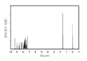
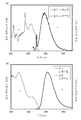


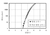

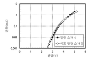


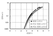


Classifications
-
- C—CHEMISTRY; METALLURGY
- C07—ORGANIC CHEMISTRY
- C07D—HETEROCYCLIC COMPOUNDS
- C07D519/00—Heterocyclic compounds containing more than one system of two or more relevant hetero rings condensed among themselves or condensed with a common carbocyclic ring system not provided for in groups C07D453/00 or C07D455/00
-
- C—CHEMISTRY; METALLURGY
- C07—ORGANIC CHEMISTRY
- C07D—HETEROCYCLIC COMPOUNDS
- C07D491/00—Heterocyclic compounds containing in the condensed ring system both one or more rings having oxygen atoms as the only ring hetero atoms and one or more rings having nitrogen atoms as the only ring hetero atoms, not provided for by groups C07D451/00 - C07D459/00, C07D463/00, C07D477/00 or C07D489/00
- C07D491/02—Heterocyclic compounds containing in the condensed ring system both one or more rings having oxygen atoms as the only ring hetero atoms and one or more rings having nitrogen atoms as the only ring hetero atoms, not provided for by groups C07D451/00 - C07D459/00, C07D463/00, C07D477/00 or C07D489/00 in which the condensed system contains two hetero rings
- C07D491/04—Ortho-condensed systems
- C07D491/044—Ortho-condensed systems with only one oxygen atom as ring hetero atom in the oxygen-containing ring
- C07D491/048—Ortho-condensed systems with only one oxygen atom as ring hetero atom in the oxygen-containing ring the oxygen-containing ring being five-membered
-
- C—CHEMISTRY; METALLURGY
- C07—ORGANIC CHEMISTRY
- C07D—HETEROCYCLIC COMPOUNDS
- C07D495/00—Heterocyclic compounds containing in the condensed system at least one hetero ring having sulfur atoms as the only ring hetero atoms
- C07D495/02—Heterocyclic compounds containing in the condensed system at least one hetero ring having sulfur atoms as the only ring hetero atoms in which the condensed system contains two hetero rings
- C07D495/04—Ortho-condensed systems
-
- C—CHEMISTRY; METALLURGY
- C09—DYES; PAINTS; POLISHES; NATURAL RESINS; ADHESIVES; COMPOSITIONS NOT OTHERWISE PROVIDED FOR; APPLICATIONS OF MATERIALS NOT OTHERWISE PROVIDED FOR
- C09K—MATERIALS FOR MISCELLANEOUS APPLICATIONS, NOT PROVIDED FOR ELSEWHERE
- C09K11/00—Luminescent, e.g. electroluminescent, chemiluminescent materials
- C09K11/06—Luminescent, e.g. electroluminescent, chemiluminescent materials containing organic luminescent materials
-
- H01L51/0071—
-
- H01L51/0073—
-
- H01L51/0074—
-
- H01L51/5012—
-
- H—ELECTRICITY
- H10—SEMICONDUCTOR DEVICES; ELECTRIC SOLID-STATE DEVICES NOT OTHERWISE PROVIDED FOR
- H10K—ORGANIC ELECTRIC SOLID-STATE DEVICES
- H10K50/00—Organic light-emitting devices
- H10K50/10—OLEDs or polymer light-emitting diodes [PLED]
- H10K50/11—OLEDs or polymer light-emitting diodes [PLED] characterised by the electroluminescent [EL] layers
-
- H—ELECTRICITY
- H10—SEMICONDUCTOR DEVICES; ELECTRIC SOLID-STATE DEVICES NOT OTHERWISE PROVIDED FOR
- H10K—ORGANIC ELECTRIC SOLID-STATE DEVICES
- H10K59/00—Integrated devices, or assemblies of multiple devices, comprising at least one organic light-emitting element covered by group H10K50/00
-
- H—ELECTRICITY
- H10—SEMICONDUCTOR DEVICES; ELECTRIC SOLID-STATE DEVICES NOT OTHERWISE PROVIDED FOR
- H10K—ORGANIC ELECTRIC SOLID-STATE DEVICES
- H10K85/00—Organic materials used in the body or electrodes of devices covered by this subclass
- H10K85/60—Organic compounds having low molecular weight
- H10K85/649—Aromatic compounds comprising a hetero atom
- H10K85/653—Aromatic compounds comprising a hetero atom comprising only oxygen as heteroatom
-
- H—ELECTRICITY
- H10—SEMICONDUCTOR DEVICES; ELECTRIC SOLID-STATE DEVICES NOT OTHERWISE PROVIDED FOR
- H10K—ORGANIC ELECTRIC SOLID-STATE DEVICES
- H10K85/00—Organic materials used in the body or electrodes of devices covered by this subclass
- H10K85/60—Organic compounds having low molecular weight
- H10K85/649—Aromatic compounds comprising a hetero atom
- H10K85/654—Aromatic compounds comprising a hetero atom comprising only nitrogen as heteroatom
-
- H—ELECTRICITY
- H10—SEMICONDUCTOR DEVICES; ELECTRIC SOLID-STATE DEVICES NOT OTHERWISE PROVIDED FOR
- H10K—ORGANIC ELECTRIC SOLID-STATE DEVICES
- H10K85/00—Organic materials used in the body or electrodes of devices covered by this subclass
- H10K85/60—Organic compounds having low molecular weight
- H10K85/649—Aromatic compounds comprising a hetero atom
- H10K85/657—Polycyclic condensed heteroaromatic hydrocarbons
- H10K85/6572—Polycyclic condensed heteroaromatic hydrocarbons comprising only nitrogen in the heteroaromatic polycondensed ring system, e.g. phenanthroline or carbazole
-
- H—ELECTRICITY
- H10—SEMICONDUCTOR DEVICES; ELECTRIC SOLID-STATE DEVICES NOT OTHERWISE PROVIDED FOR
- H10K—ORGANIC ELECTRIC SOLID-STATE DEVICES
- H10K85/00—Organic materials used in the body or electrodes of devices covered by this subclass
- H10K85/60—Organic compounds having low molecular weight
- H10K85/649—Aromatic compounds comprising a hetero atom
- H10K85/657—Polycyclic condensed heteroaromatic hydrocarbons
- H10K85/6574—Polycyclic condensed heteroaromatic hydrocarbons comprising only oxygen in the heteroaromatic polycondensed ring system, e.g. cumarine dyes
-
- H—ELECTRICITY
- H10—SEMICONDUCTOR DEVICES; ELECTRIC SOLID-STATE DEVICES NOT OTHERWISE PROVIDED FOR
- H10K—ORGANIC ELECTRIC SOLID-STATE DEVICES
- H10K85/00—Organic materials used in the body or electrodes of devices covered by this subclass
- H10K85/60—Organic compounds having low molecular weight
- H10K85/649—Aromatic compounds comprising a hetero atom
- H10K85/657—Polycyclic condensed heteroaromatic hydrocarbons
- H10K85/6576—Polycyclic condensed heteroaromatic hydrocarbons comprising only sulfur in the heteroaromatic polycondensed ring system, e.g. benzothiophene
-
- H—ELECTRICITY
- H10—SEMICONDUCTOR DEVICES; ELECTRIC SOLID-STATE DEVICES NOT OTHERWISE PROVIDED FOR
- H10K—ORGANIC ELECTRIC SOLID-STATE DEVICES
- H10K2101/00—Properties of the organic materials covered by group H10K85/00
- H10K2101/10—Triplet emission
-
- H—ELECTRICITY
- H10—SEMICONDUCTOR DEVICES; ELECTRIC SOLID-STATE DEVICES NOT OTHERWISE PROVIDED FOR
- H10K—ORGANIC ELECTRIC SOLID-STATE DEVICES
- H10K50/00—Organic light-emitting devices
- H10K50/10—OLEDs or polymer light-emitting diodes [PLED]
- H10K50/11—OLEDs or polymer light-emitting diodes [PLED] characterised by the electroluminescent [EL] layers
- H10K50/125—OLEDs or polymer light-emitting diodes [PLED] characterised by the electroluminescent [EL] layers specially adapted for multicolour light emission, e.g. for emitting white light
- H10K50/13—OLEDs or polymer light-emitting diodes [PLED] characterised by the electroluminescent [EL] layers specially adapted for multicolour light emission, e.g. for emitting white light comprising stacked EL layers within one EL unit
-
- H—ELECTRICITY
- H10—SEMICONDUCTOR DEVICES; ELECTRIC SOLID-STATE DEVICES NOT OTHERWISE PROVIDED FOR
- H10K—ORGANIC ELECTRIC SOLID-STATE DEVICES
- H10K85/00—Organic materials used in the body or electrodes of devices covered by this subclass
- H10K85/30—Coordination compounds
- H10K85/341—Transition metal complexes, e.g. Ru(II)polypyridine complexes
- H10K85/342—Transition metal complexes, e.g. Ru(II)polypyridine complexes comprising iridium
Abstract
신규 유기 화합물인 벤조퓨로피리미딘 유도체 또는 벤조티에노피리미딘 유도체를 제공한다. 하기 일반식(G1)으로 나타내어지는 유기 화합물이다.

또한, 일반식(G1)에 있어서, Q는 산소 또는 황을 나타낸다. 또한, A는 총탄소수 12 내지 100의 기이고, 또한 벤젠 고리, 나프탈렌 고리, 플루오렌 고리, 페난트렌 고리, 트라이페닐렌 고리, 다이벤조싸이오펜 고리를 포함하는 헤테로 방향족 고리, 다이벤조퓨란 고리를 포함하는 헤테로 방향족 고리, 카바졸 고리를 포함하는 헤테로 방향족 고리, 벤즈이미다졸 고리, 트라이페닐아민 구조 중 어느 하나 또는 복수를 가진다.It provides a novel organic compound, a benzofuropyrimidine derivative or a benzothienopyrimidine derivative. It is an organic compound represented by the following general formula (G1).
In addition, in General Formula (G1), Q represents oxygen or sulfur. In addition, A is a group having a total carbon number of 12 to 100, and a benzene ring, a naphthalene ring, a fluorene ring, a phenanthrene ring, a triphenylene ring, a heteroaromatic ring including a dibenzothiophene ring, and a dibenzofuran ring. It has any one or more of a heteroaromatic ring including, a heteroaromatic ring including a carbazole ring, a benzimidazole ring, and a triphenylamine structure.

Description
본 발명의 일 형태는 유기 화합물, 발광 소자, 발광 장치, 전자 기기, 및 조명 장치에 관한 것이다. 다만, 본 발명의 일 형태는 상기 기술분야에 한정되지 않는다. 즉 본 발명의 일 형태는 물건, 방법, 제조 방법, 또는 구동 방법에 관한 것이다. 또는, 본 발명의 일 형태는 공정(process), 기계(machine), 제품(manufacture), 또는 조성물(composition of matter)에 관한 것이다. 또한 구체적으로는, 반도체 장치, 표시 장치, 액정 표시 장치 등을 일례로서 들 수 있다.One embodiment of the present invention relates to an organic compound, a light emitting device, a light emitting device, an electronic device, and a lighting device. However, one embodiment of the present invention is not limited to the above technical field. That is, one aspect of the present invention relates to an object, a method, a manufacturing method, or a driving method. Or, one aspect of the present invention relates to a process, a machine, a manufacture, or a composition of matter. Moreover, specifically, a semiconductor device, a display device, a liquid crystal display device, etc. are mentioned as an example.
한 쌍의 전극 사이에 EL층을 끼워 이루어지는 발광 소자(유기 EL 소자라고도 함)는, 박형 경량, 입력 신호에 대한 고속 응답성, 저소비전력 등의 특성을 가지기 때문에, 이들이 적용된 디스플레이는 차세대 플랫 패널 디스플레이로서 주목을 받고 있다.Light-emitting elements (also referred to as organic EL elements) formed by sandwiching an EL layer between a pair of electrodes have characteristics such as thinness, light weight, high-speed response to input signals, and low power consumption, so the displays to which these are applied are next-generation flat panel displays. Is attracting attention.
발광 소자는 한 쌍의 전극 사이에 전압을 인가함으로써, 각 전극으로부터 주입된 전자 및 정공이 EL층에서 재결합하여, EL층에 포함되는 발광 물질(유기 화합물)이 들뜬 상태가 되고, 그 들뜬 상태가 바닥 상태로 되돌아갈 때에 발광한다. 또한, 들뜬 상태의 종류로서는, 단일항 들뜬 상태(S*)와 삼중항 들뜬 상태(T*)가 있고, 단일항 들뜬 상태로부터의 발광이 형광, 삼중항 들뜬 상태로부터의 발광이 인광이라고 불리고 있다. 또한, 발광 소자에서의 그들의 통계적인 생성 비율은 S*:T*=1:3인 것으로 생각된다. 발광 물질로부터 얻어지는 발광 스펙트럼은 그 발광 물질 특유의 것이고, 상이한 종류의 유기 화합물을 발광 물질로서 사용함으로써, 다양한 발광색의 발광 소자를 얻을 수 있다.In the light-emitting element, by applying a voltage between a pair of electrodes, electrons and holes injected from each electrode recombine in the EL layer, and the light-emitting material (organic compound) contained in the EL layer becomes excited, and the excited state is reduced. It glows when it returns to the ground state. In addition, as the type of excited state, there are singlet excited state (S * ) and triplet excited state (T * ), and light emission from the singlet excited state is called fluorescence, and light emission from the triplet excited state is called phosphorescence. . In addition, it is considered that their statistical production ratio in the light emitting device is S * :T * = 1:3. The light emission spectrum obtained from the light-emitting material is peculiar to the light-emitting material, and by using different kinds of organic compounds as the light-emitting material, light-emitting elements of various light-emitting colors can be obtained.
이와 같은 발광 소자에 관해서는, 그 소자 특성을 향상시키기 위하여 소자 구조의 개량이나 재료 개발 등이 활발히 진행되고 있다(예를 들어, 특허문헌 1 참조).Regarding such a light-emitting device, in order to improve the device characteristics, improvement of the device structure, material development, and the like are actively progressing (see, for example, Patent Document 1).
그러므로, 본 발명의 일 형태에서는 신규 유기 화합물을 제공한다. 또한, 본 발명의 다른 일 형태에서는 신규 유기 화합물인 벤조퓨로피리미딘 골격 또는 벤조티에노피리미딘 유도체를 제공한다. 또한, 본 발명의 일 형태에서는 발광 소자에 사용할 수 있는 신규 유기 화합물을 제공한다. 또한, 본 발명의 일 형태에서는 발광 소자의 EL층에 사용할 수 있는 신규 유기 화합물을 제공한다. 또한, 본 발명의 일 형태인 신규 유기 화합물을 사용한 신뢰성이 높은 신규 발광 소자를 제공한다. 또한, 신규 발광 장치, 신규 전자 기기, 또는 신규 조명 장치를 제공한다. 또한, 이들 과제의 기재는 다른 과제의 존재를 방해하는 것은 아니다. 또한, 본 발명의 일 형태는 이들 과제 모두를 반드시 해결할 필요는 없다. 또한, 이들 이외의 과제는 명세서, 도면, 청구항 등의 기재로부터 저절로 명백해지는 것이며 명세서, 도면, 청구항 등의 기재로부터 이들 이외의 과제를 추출할 수 있다.Therefore, in one aspect of the present invention, a novel organic compound is provided. In addition, another aspect of the present invention provides a novel organic compound such as a benzofuropyrimidine skeleton or a benzothienopyrimidine derivative. In addition, one embodiment of the present invention provides a novel organic compound that can be used in a light emitting device. In addition, one embodiment of the present invention provides a novel organic compound that can be used in the EL layer of a light emitting device. Further, a novel light emitting device with high reliability using a novel organic compound, which is one embodiment of the present invention, is provided. Further, a new light emitting device, a new electronic device, or a new lighting device is provided. In addition, description of these problems does not interfere with the existence of other problems. In addition, one embodiment of the present invention does not necessarily have to solve all of these problems. In addition, problems other than these will become apparent from description of the specification, drawings, claims, and the like, and subjects other than these can be extracted from the description of the specification, drawings, and claims.
본 발명의 일 형태는 벤조퓨로피리미딘 유도체 또는 벤조티에노피리미딘 유도체이고, 하기 일반식(G1)으로 나타내어지는 유기 화합물이다. 또한, 하기 일반식(G1)으로 나타내어지는 바와 같이, 벤조퓨로피리미딘 골격 또는 벤조티에노피리미딘 골격의 8위치에 비치환된 페닐기를 가지는 구조이다.One embodiment of the present invention is a benzofuropyrimidine derivative or a benzothienopyrimidine derivative, and is an organic compound represented by the following general formula (G1). Further, as represented by the following general formula (G1), it is a structure having an unsubstituted phenyl group at the 8 position of a benzofuropyrimidine skeleton or a benzothienopyrimidine skeleton.
[화학식 1][Formula 1]

상기 일반식(G1)에 있어서, Q는 산소 또는 황을 나타낸다. 또한, A는 총탄소수 12 내지 100의 기이고, 또한 벤젠 고리, 나프탈렌 고리, 플루오렌 고리, 페난트렌 고리, 트라이페닐렌 고리, 다이벤조싸이오펜 고리를 포함하는 헤테로 방향족 고리, 다이벤조퓨란 고리를 포함하는 헤테로 방향족 고리, 카바졸 고리를 포함하는 헤테로 방향족 고리, 벤즈이미다졸 고리, 트라이페닐아민 구조 중 어느 하나 또는 복수를 가진다. 또한, R1은 수소, 탄소수 1 내지 6의 알킬기, 치환 또는 비치환된 탄소수 5 내지 7의 단일 고리식 포화 탄화수소, 치환 또는 비치환된 탄소수 7 내지 10의 다환식 포화 탄화수소, 치환 또는 비치환된 탄소수 6 내지 13의 아릴기, 또는 치환 또는 비치환된 탄소수 3 내지 12의 헤테로아릴기를 나타낸다.In the general formula (G1), Q represents oxygen or sulfur. In addition, A is a group having a total carbon number of 12 to 100, and a benzene ring, a naphthalene ring, a fluorene ring, a phenanthrene ring, a triphenylene ring, a heteroaromatic ring including a dibenzothiophene ring, and a dibenzofuran ring. It has any one or more of a heteroaromatic ring including, a heteroaromatic ring including a carbazole ring, a benzimidazole ring, and a triphenylamine structure. In addition, R 1 is hydrogen, an alkyl group having 1 to 6 carbon atoms, a substituted or unsubstituted monocyclic saturated hydrocarbon having 5 to 7 carbon atoms, a substituted or unsubstituted polycyclic saturated hydrocarbon having 7 to 10 carbon atoms, a substituted or unsubstituted It represents a C6-C13 aryl group or a substituted or unsubstituted C3-C12 heteroaryl group.
또한, 본 발명의 다른 일 형태는 벤조퓨로피리미딘 유도체 또는 벤조티에노피리미딘 유도체이고, 하기 일반식(G2)으로 나타내어지는 유기 화합물이다. 또한, 하기 일반식(G2)으로 나타내어지는 바와 같이, 벤조퓨로피리미딘 골격 또는 벤조티에노피리미딘 골격의 8위치에 비치환된 페닐기를 가지는 구조이다.Further, another embodiment of the present invention is a benzofuropyrimidine derivative or a benzothienopyrimidine derivative, and is an organic compound represented by the following general formula (G2). Further, as represented by the following general formula (G2), it is a structure having an unsubstituted phenyl group at the 8 position of the benzofuropyrimidine skeleton or the benzothienopyrimidine skeleton.
[화학식 2][Formula 2]

상기 일반식(G2)에 있어서, Q는 산소 또는 황을 나타낸다. 또한, α는 치환 또는 비치환된 페닐렌기를 나타내고, n은 0 내지 4의 정수를 나타낸다. 또한, Htuni는 정공 수송성을 가지는 골격을 나타낸다. 또한, R1은 수소, 탄소수 1 내지 6의 알킬기, 치환 또는 비치환된 탄소수 5 내지 7의 단일 고리식 포화 탄화수소, 치환 또는 비치환된 탄소수 7 내지 10의 다환식 포화 탄화수소, 치환 또는 비치환된 탄소수 6 내지 13의 아릴기, 또는 치환 또는 비치환된 탄소수 3 내지 12의 헤테로아릴기를 나타낸다.In the general formula (G2), Q represents oxygen or sulfur. In addition, α represents a substituted or unsubstituted phenylene group, and n represents an integer of 0 to 4. In addition, Ht uni represents a skeleton having hole transport properties. In addition, R 1 is hydrogen, an alkyl group having 1 to 6 carbon atoms, a substituted or unsubstituted monocyclic saturated hydrocarbon having 5 to 7 carbon atoms, a substituted or unsubstituted polycyclic saturated hydrocarbon having 7 to 10 carbon atoms, a substituted or unsubstituted It represents a C6-C13 aryl group or a substituted or unsubstituted C3-C12 heteroaryl group.
또한, 본 발명의 다른 일 형태는, 벤조퓨로피리미딘 유도체 또는 벤조티에노피리미딘 유도체이고, 하기 일반식(G3)으로 나타내어지는 유기 화합물이다. 또한, 하기 일반식(G3)으로 나타내어지는 바와 같이, 벤조퓨로피리미딘 골격 또는 벤조티에노피리미딘 골격의 8위치에 비치환된 페닐기를 가지는 구조이다.Further, another aspect of the present invention is a benzofuropyrimidine derivative or a benzothienopyrimidine derivative, and is an organic compound represented by the following general formula (G3). Further, as represented by the following general formula (G3), it is a structure having a phenyl group unsubstituted at the 8 position of the benzofuropyrimidine skeleton or the benzothienopyrimidine skeleton.
[화학식 3][Formula 3]

상기 일반식(G3)에 있어서, Q는 산소 또는 황을 나타낸다. 또한, Htuni는 정공 수송성을 가지는 골격을 나타낸다. 또한, R1은 수소, 탄소수 1 내지 6의 알킬기, 치환 또는 비치환된 탄소수 5 내지 7의 단일 고리식 포화 탄화수소, 치환 또는 비치환된 탄소수 7 내지 10의 다환식 포화 탄화수소, 치환 또는 비치환된 탄소수 6 내지 13의 아릴기, 또는 치환 또는 비치환된 탄소수 3 내지 12의 헤테로아릴기를 나타낸다.In the general formula (G3), Q represents oxygen or sulfur. In addition, Ht uni represents a skeleton having hole transport properties. In addition, R 1 is hydrogen, an alkyl group having 1 to 6 carbon atoms, a substituted or unsubstituted monocyclic saturated hydrocarbon having 5 to 7 carbon atoms, a substituted or unsubstituted polycyclic saturated hydrocarbon having 7 to 10 carbon atoms, a substituted or unsubstituted It represents a C6-C13 aryl group or a substituted or unsubstituted C3-C12 heteroaryl group.
또한, 본 발명의 다른 일 형태는 벤조퓨로피리미딘 유도체 또는 벤조티에노피리미딘 유도체이고, 하기 일반식(G4)으로 나타내어지는 유기 화합물이다. 또한, 하기 일반식(G4)으로 나타내어지는 바와 같이, 벤조퓨로피리미딘 골격 또는 벤조티에노피리미딘 골격의 8위치에 비치환된 페닐기를 가지는 구조이다.Further, another aspect of the present invention is a benzofuropyrimidine derivative or a benzothienopyrimidine derivative, and is an organic compound represented by the following general formula (G4). Further, as represented by the following general formula (G4), it is a structure having a phenyl group unsubstituted at the 8 position of the benzofuropyrimidine skeleton or the benzothienopyrimidine skeleton.
[화학식 4][Formula 4]

상기 일반식(G4)에 있어서, Q는 산소 또는 황을 나타낸다. 또한, Htuni는 정공 수송성을 가지는 골격을 나타낸다. 또한, R1은 수소, 탄소수 1 내지 6의 알킬기, 치환 또는 비치환된 탄소수 5 내지 7의 단일 고리식 포화 탄화수소, 치환 또는 비치환된 탄소수 7 내지 10의 다환식 포화 탄화수소, 치환 또는 비치환된 탄소수 6 내지 13의 아릴기, 또는 치환 또는 비치환된 탄소수 3 내지 12의 헤테로아릴기를 나타낸다.In the general formula (G4), Q represents oxygen or sulfur. In addition, Ht uni represents a skeleton having hole transport properties. In addition, R 1 is hydrogen, an alkyl group having 1 to 6 carbon atoms, a substituted or unsubstituted monocyclic saturated hydrocarbon having 5 to 7 carbon atoms, a substituted or unsubstituted polycyclic saturated hydrocarbon having 7 to 10 carbon atoms, a substituted or unsubstituted It represents a C6-C13 aryl group or a substituted or unsubstituted C3-C12 heteroaryl group.
또한, 상기 각 구성에 있어서, 상기 일반식(G2), (G3), 및 (G4) 중의 Htuni는 각각 독립적으로 피롤 고리 구조, 퓨란 고리 구조, 또는 싸이오펜 고리 구조 중 어느 하나를 가진다.In addition, in each of the above configurations, Ht uni in the general formulas (G2), (G3), and (G4) each independently has any one of a pyrrole ring structure, a furan ring structure, or a thiophene ring structure.
또한, 상기 각 구성에 있어서, 상기 일반식(G2), (G3), 및 (G4) 중의 Htuni는 각각 독립적으로 하기 일반식(Ht-1) 내지 (Ht-26) 중 어느 하나이다.In addition, in each of the above configurations, Ht uni in the general formulas (G2), (G3), and (G4) is each independently any one of the following general formulas (Ht-1) to (Ht-26).
[화학식 5][Formula 5]

또한, 상기 일반식(Ht-1) 내지 일반식(Ht-26)에 있어서, Q는 산소 또는 황을 나타낸다. 또한, R2 내지 R71은 각각 1 내지 4의 치환기를 나타내고, 또한 각각 독립적으로 수소, 탄소수 1 내지 6의 알킬기, 치환 또는 비치환된 페닐기 중 어느 하나를 나타낸다. 또한, Ar1은 치환 또는 비치환된 탄소수 6 내지 13의 아릴기를 나타낸다.In addition, in the general formulas (Ht-1) to (Ht-26), Q represents oxygen or sulfur. Further, R 2 to R 71 each represents a substituent of 1 to 4, and each independently represents hydrogen, an alkyl group having 1 to 6 carbon atoms, or a substituted or unsubstituted phenyl group. In addition, Ar 1 represents a substituted or unsubstituted aryl group having 6 to 13 carbon atoms.
또한 본 발명의 다른 일 형태는 구조식(100, 101, 102, 117, 또는 200) 중 어느 하나로 나타내어지는 유기 화합물이다.In addition, another aspect of the present invention is an organic compound represented by any one of structural formulas (100, 101, 102, 117, or 200).
[화학식 6][Formula 6]

또한, 본 발명의 다른 일 형태는 상술한 본 발명의 일 형태인 유기 화합물을 사용한 발광 소자이다. 또한, 상기 유기 화합물에 더하여 게스트 재료를 가지는 발광 소자도 본 발명에 포함한다.In addition, another aspect of the present invention is a light emitting device using the organic compound, which is one aspect of the present invention described above. Further, in addition to the organic compound, a light emitting device having a guest material is also included in the present invention.
본 발명의 다른 일 형태는, 상술한 본 발명의 일 형태인 유기 화합물을 사용한 발광 소자이다. 또한, 한 쌍의 전극 사이에 가지는 EL층이나, EL층에 포함되는 발광층에 본 발명의 일 형태인 유기 화합물을 사용하여 형성된 발광 소자도 본 발명에 포함되는 것으로 한다. 또한, 상기 발광 소자에 더하여, 전극과 접하여 유기화합물을 가지는 층(예를 들어 캡층)을 가지는 경우도 발광 소자에 포함하고, 본 발명에 포함되는 것으로 한다. 또한, 발광 소자에 더하여, 트랜지스터, 기판 등을 가지는 발광 장치도 발명의 범주에 포함된다. 또한, 이들 발광 장치에 더하여, 마이크로폰, 카메라, 조작용 버튼, 외부 접속부, 하우징, 커버, 지지대, 또는 스피커 등을 가지는 전자 기기나 조명 장치도 발명의 범주에 포함된다.Another aspect of the present invention is a light emitting device using the organic compound which is one aspect of the present invention described above. In addition, a light-emitting element formed by using an organic compound as an embodiment of the present invention in an EL layer provided between a pair of electrodes or a light-emitting layer included in the EL layer is also included in the present invention. In addition, in addition to the light-emitting device, a case in which a layer having an organic compound (eg, a cap layer) in contact with the electrode is included in the light-emitting device and is included in the present invention. In addition to the light-emitting element, a light-emitting device having a transistor, a substrate, or the like is also included in the scope of the invention. Further, in addition to these light-emitting devices, electronic devices and lighting devices having a microphone, a camera, a button for operation, an external connection, a housing, a cover, a support, or a speaker are also included in the scope of the invention.
또한, 본 발명의 일 형태는 발광 소자를 가지는 발광 장치를 포함하고, 또한 발광 장치를 가지는 조명 장치도 범주에 포함하는 것으로 한다. 따라서, 본 명세서에서 발광 장치란, 화상 표시 디바이스 또는 광원(조명 장치를 포함함)을 가리킨다. 또한, 발광 장치에, 예를 들어 FPC(Flexible printed circuit) 또는 TCP(Tape Carrier Package) 등의 커넥터가 장착된 모듈, TCP 끝에 인쇄 배선판이 제공된 모듈, 또는 발광 소자에 COG(Chip On Glass) 방식으로 IC(집적 회로)가 직접 실장된 모듈도 모두 발광 장치에 포함되는 것으로 한다.In addition, one embodiment of the present invention includes a light-emitting device having a light-emitting element, and also includes a lighting device having a light-emitting device in the category. Therefore, in this specification, the light emitting device refers to an image display device or a light source (including a lighting device). In addition, in the light emitting device, for example, a module equipped with a connector such as FPC (Flexible printed circuit) or TCP (Tape Carrier Package), a module provided with a printed wiring board at the end of the TCP, or a COG (Chip On Glass) method in the light emitting device. All modules in which an IC (integrated circuit) is directly mounted are also included in the light emitting device.
본 발명의 일 형태에서는 신규 유기 화합물을 제공할 수 있다. 또한, 본 발명의 다른 일 형태에서는 신규 유기 화합물인 벤조퓨로피리미딘 유도체 또는 벤조티에노피리미딘 유도체를 제공할 수 있다. 또한, 본 발명의 일 형태에서는 발광 소자에 사용할 수 있는 신규 유기 화합물을 제공할 수 있다. 또한, 본 발명의 일 형태에서는 발광 소자의 EL층에 사용할 수 있는 신규 유기 화합물을 제공할 수 있다. 또한, 본 발명의 일 형태인 신규 유기 화합물을 사용함으로써 신뢰성이 높은 신규 발광 소자를 제공할 수 있다. 또한, 신규 발광 장치, 신규 전자 기기, 또는 신규 조명 장치를 제공할 수 있다.In one embodiment of the present invention, a novel organic compound can be provided. In addition, in another embodiment of the present invention, a novel organic compound such as a benzofuropyrimidine derivative or a benzothienopyrimidine derivative may be provided. In addition, in one embodiment of the present invention, a novel organic compound that can be used in a light emitting device can be provided. In addition, in one embodiment of the present invention, a novel organic compound that can be used in the EL layer of a light emitting device can be provided. In addition, a novel light-emitting device with high reliability can be provided by using a novel organic compound as an embodiment of the present invention. In addition, a new light emitting device, a new electronic device, or a new lighting device can be provided.
도 1은 발광 소자의 구조에 대하여 설명한 도면.
도 2는 발광 장치에 대하여 설명한 도면.
도 3은 발광 장치에 대하여 설명한 도면.
도 4는 전자 기기에 대하여 설명한 도면.
도 5는 전자 기기에 대하여 설명한 도면.
도 6은 자동차에 대하여 설명한 도면.
도 7은 조명 장치에 대하여 설명한 도면.
도 8은 구조식(100)으로 나타낸 유기 화합물의 1H-NMR 차트.
도 9는 구조식(100)으로 나타낸 유기 화합물의 자외·가시 흡수 스펙트럼 및 발광 스펙트럼.
도 10은 구조식(101)으로 나타낸 유기 화합물의 1H-NMR 차트.
도 11은 구조식(101)으로 나타낸 유기 화합물의 자외·가시 흡수 스펙트럼 및 발광 스펙트럼.
도 12는 구조식(102)으로 나타낸 유기 화합물의 1H-NMR 차트.
도 13은 구조식(200)으로 나타낸 유기 화합물의 1H-NMR 차트.
도 14는 발광 소자에 대하여 설명한 도면.
도 15는 발광 소자 1, 비교 발광 소자 2, 및 비교 발광 소자 3의 전류 밀도-휘도 특성을 나타낸 도면.
도 16은 발광 소자 1, 비교 발광 소자 2, 및 비교 발광 소자 3의 전압-휘도 특성을 나타낸 도면.
도 17은 발광 소자 1, 비교 발광 소자 2, 및 비교 발광 소자 3의 휘도-전류 효율 특성을 나타낸 도면.
도 18은 발광 소자 1, 비교 발광 소자 2, 및 비교 발광 소자 3의 전압-전류 특성을 나타낸 도면.
도 19는 발광 소자 1, 비교 발광 소자 2, 및 비교 발광 소자 3의 발광 스펙트럼을 나타낸 도면.
도 20은 발광 소자 1, 비교 발광 소자 2, 및 비교 발광 소자 3의 신뢰성을 나타낸 도면.
도 21은 발광 소자 4 및 비교 발광 소자 5의 전류 밀도-휘도 특성을 나타낸 도면.
도 22는 발광 소자 4 및 비교 발광 소자 5의 전압-휘도 특성을 나타낸 도면.
도 23은 발광 소자 4 및 비교 발광 소자 5의 휘도-전류 효율 특성을 나타낸 도면.
도 24는 발광 소자 4 및 비교 발광 소자 5의 전압-전류 특성을 나타낸 도면.
도 25는 발광 소자 4 및 비교 발광 소자 5의 발광 스펙트럼을 나타낸 도면.
도 26은 발광 소자 4 및 비교 발광 소자 5의 신뢰성을 나타낸 도면.
도 27은 발광 소자 6, 비교 발광 소자 7, 및 비교 발광 소자 8의 전류 밀도-휘도 특성을 나타낸 도면.
도 28은 발광 소자 6, 비교 발광 소자 7, 및 비교 발광 소자 8의 전압-휘도 특성을 나타낸 도면.
도 29는 발광 소자 6, 비교 발광 소자 7, 및 비교 발광 소자 8의 휘도-전류 효율 특성을 나타낸 도면.
도 30은 발광 소자 6, 비교 발광 소자 7, 및 비교 발광 소자 8의 전압-전류 특성을 나타낸 도면.
도 31은 발광 소자 6, 비교 발광 소자 7, 및 비교 발광 소자 8의 발광 스펙트럼을 나타낸 도면.
도 32는 발광 소자 6, 비교 발광 소자 7, 및 비교 발광 소자 8의 신뢰성을 나타낸 도면.
도 33은 구조식(117)으로 나타낸 유기 화합물의 1H-NMR 차트.
도 34는 발광 소자 9의 전류 밀도-휘도 특성을 나타낸 도면.
도 35는 발광 소자 9의 전압-휘도 특성을 나타낸 도면.
도 36은 발광 소자 9의 휘도-전류 효율 특성을 나타낸 도면.
도 37은 발광 소자 9의 전압-전류 특성을 나타낸 도면.
도 38은 발광 소자 9의 발광 스펙트럼을 나타낸 도면.1 is a view explaining the structure of a light emitting device.
2 is a view explaining a light emitting device.
3 is a diagram explaining a light emitting device.
4 is a diagram illustrating an electronic device.
5 is a diagram explaining an electronic device.
6 is a view explaining a vehicle.
7 is a diagram explaining a lighting device.
8 is a 1 H-NMR chart of an organic compound represented by Structural Formula (100).
9 is an ultraviolet/visible absorption spectrum and emission spectrum of an organic compound represented by Structural Formula (100).
10 is a 1 H-NMR chart of an organic compound represented by Structural Formula (101).
11 is an ultraviolet/visible absorption spectrum and emission spectrum of an organic compound represented by structural formula (101).
12 is a 1 H-NMR chart of an organic compound represented by structural formula (102).
13 is a 1 H-NMR chart of an organic compound represented by structural formula (200).
14 is a diagram explaining a light-emitting element.
15 is a view showing current density-luminance characteristics of Light-Emitting
16 is a view showing voltage-luminance characteristics of Light-Emitting
17 is a view showing luminance-current efficiency characteristics of Light-Emitting
18 is a view showing voltage-current characteristics of Light-Emitting
19 is a view showing emission spectra of Light-Emitting
20 is a diagram showing the reliability of Light-Emitting
21 is a view showing current density-luminance characteristics of Light-Emitting
22 is a view showing voltage-luminance characteristics of Light-Emitting
23 is a diagram showing luminance-current efficiency characteristics of Light-Emitting
24 is a view showing voltage-current characteristics of Light-Emitting
25 is a diagram showing emission spectra of Light-Emitting
26 is a diagram showing the reliability of Light-Emitting
27 is a view showing current density-luminance characteristics of Light-Emitting
28 is a diagram showing voltage-luminance characteristics of Light-Emitting
29 is a view showing luminance-current efficiency characteristics of Light-Emitting
30 is a diagram showing voltage-current characteristics of Light-Emitting
31 is a view showing emission spectra of Light-Emitting
Fig. 32 is a diagram showing the reliability of Light-Emitting
33 is a 1 H-NMR chart of an organic compound represented by Structural Formula (117).
34 is a view showing current density-luminance characteristics of Light-Emitting
35 is a view showing voltage-luminance characteristics of Light-Emitting
36 is a view showing luminance-current efficiency characteristics of Light-Emitting
37 is a diagram showing voltage-current characteristics of Light-Emitting
38 is a diagram showing an emission spectrum of Light-Emitting
이하, 본 발명의 실시형태에 대하여 도면을 사용하여 자세히 설명한다. 다만, 본 발명은 이하의 설명에 한정되지 않고, 본 발명의 취지 및 그 범위에서 벗어남이 없이 그 형태 및 자세한 사항을 다양하게 변경할 수 있다. 따라서 본 발명은 이하에 나타내는 실시형태의 기재 내용에 한정되어 해석되는 것은 아니다.Hereinafter, embodiments of the present invention will be described in detail with reference to the drawings. However, the present invention is not limited to the following description, and the form and details can be variously changed without departing from the spirit and scope of the present invention. Therefore, the present invention is not interpreted as being limited to the description of the embodiments shown below.
또한, 도면 등에 나타낸 각 구성의 위치, 크기, 범위 등은 이해하기 쉽게 하기 위하여 실제의 위치, 크기, 범위 등을 나타내지 않는 경우가 있다. 따라서, 개시(開示)하는 발명은 도면 등에 개시된 위치, 크기, 범위 등에 반드시 한정되지는 않는다.In addition, the location, size, range, etc. of each component shown in the drawings or the like may not indicate the actual location, size, range, etc. for easy understanding. Accordingly, the disclosed invention is not necessarily limited to the position, size, and range disclosed in the drawings or the like.
또한, 본 명세서 등에서 도면을 사용하여 발명의 구성을 설명하는 데 있어서, 같은 것을 가리키는 부호는 상이한 도면 간에서도 공통적으로 사용한다.In addition, in describing the configuration of the invention using the drawings in this specification and the like, reference numerals indicating the same are used in common among different drawings.
(실시형태 1)(Embodiment 1)
본 실시형태에서는 본 발명의 일 형태인 유기 화합물에 대하여 설명한다. 또한, 본 발명의 일 형태인 유기 화합물은 하기 일반식(G1)으로 나타내어지는, 벤조퓨로피리미딘 유도체 또는 벤조티에노피리미딘 유도체이다. 또한, 본 발명의 일 형태인 유기 화합물은 하기 일반식(G1)으로 나타내어지는 것과 같이 벤조퓨로피리미딘 골격 또는 벤조티에노피리미딘 골격의 8위치에 비치환된 페닐기를 가지는 구조이다.In this embodiment, an organic compound which is one embodiment of the present invention will be described. Further, the organic compound which is one embodiment of the present invention is a benzofuropyrimidine derivative or a benzothienopyrimidine derivative represented by the following general formula (G1). In addition, the organic compound as an embodiment of the present invention has a structure having a phenyl group unsubstituted at the 8 position of the benzofuropyrimidine skeleton or the benzothienopyrimidine skeleton as represented by the following general formula (G1).
[화학식 7][Formula 7]

또한, 일반식(G1)에 있어서 Q는 산소 또는 황을 나타낸다. 또한, A는 총탄소수 12 내지 100의 기이고, 또한 벤젠 고리, 나프탈렌 고리, 플루오렌 고리, 페난트렌 고리, 트라이페닐렌 고리, 다이벤조싸이오펜 고리를 포함하는 헤테로 방향족 고리, 다이벤조퓨란 고리를 포함하는 헤테로 방향족 고리, 카바졸 고리를 포함하는 헤테로 방향족 고리, 벤즈이미다졸 고리, 트라이페닐아민 구조 중 어느 하나 또는 복수를 가진다. 또한, R1은 수소, 탄소수 1 내지 6의 알킬기, 치환 또는 비치환된 탄소수 5 내지 7의 단일 고리식 포화 탄화수소, 치환 또는 비치환된 탄소수 7 내지 10의 다환식 포화 탄화수소, 치환 또는 비치환된 탄소수 6 내지 13의 아릴기, 또는 치환 또는 비치환된 탄소수 3 내지 12의 헤테로아릴기를 나타낸다.In addition, in General Formula (G1), Q represents oxygen or sulfur. In addition, A is a group having a total carbon number of 12 to 100, and a benzene ring, a naphthalene ring, a fluorene ring, a phenanthrene ring, a triphenylene ring, a heteroaromatic ring including a dibenzothiophene ring, and a dibenzofuran ring. It has any one or more of a heteroaromatic ring including, a heteroaromatic ring including a carbazole ring, a benzimidazole ring, and a triphenylamine structure. In addition, R 1 is hydrogen, an alkyl group having 1 to 6 carbon atoms, a substituted or unsubstituted monocyclic saturated hydrocarbon having 5 to 7 carbon atoms, a substituted or unsubstituted polycyclic saturated hydrocarbon having 7 to 10 carbon atoms, a substituted or unsubstituted It represents a C6-C13 aryl group or a substituted or unsubstituted C3-C12 heteroaryl group.
또한, 본 발명의 다른 일 형태는 하기 일반식(G2)으로 나타내어지는 유기 화합물이다.In addition, another aspect of the present invention is an organic compound represented by the following general formula (G2).
[화학식 8][Formula 8]

상기 일반식(G2)에 있어서, Q는 산소 또는 황을 나타낸다. 또한, α는 치환 또는 비치환된 페닐렌기를 나타내고, n은 0 내지 4의 정수를 나타낸다. 또한, Htuni는 정공 수송성을 가지는 골격을 나타낸다. 또한, R1은 수소, 탄소수 1 내지 6의 알킬기, 치환 또는 비치환된 탄소수 5 내지 7의 단일 고리식 포화 탄화수소, 치환 또는 비치환된 탄소수 7 내지 10의 다환식 포화 탄화수소, 치환 또는 비치환된 탄소수 6 내지 13의 아릴기, 또는 치환 또는 비치환된 탄소수 3 내지 12의 헤테로아릴기를 나타낸다.In the general formula (G2), Q represents oxygen or sulfur. In addition, α represents a substituted or unsubstituted phenylene group, and n represents an integer of 0 to 4. In addition, Ht uni represents a skeleton having hole transport properties. In addition, R 1 is hydrogen, an alkyl group having 1 to 6 carbon atoms, a substituted or unsubstituted monocyclic saturated hydrocarbon having 5 to 7 carbon atoms, a substituted or unsubstituted polycyclic saturated hydrocarbon having 7 to 10 carbon atoms, a substituted or unsubstituted It represents a C6-C13 aryl group or a substituted or unsubstituted C3-C12 heteroaryl group.
또한, 본 발명의 다른 일 형태는 하기 일반식(G3)으로 나타내어지는 유기 화합물이다.In addition, another aspect of the present invention is an organic compound represented by the following general formula (G3).
[화학식 9][Formula 9]

상기 일반식(G3)에 있어서, Q는 산소 또는 황을 나타낸다. 또한, Htuni는 정공 수송성을 가지는 골격을 나타낸다. 또한, R1은, 수소, 탄소수 1 내지 6의 알킬기, 치환 또는 비치환된 탄소수 5 내지 7의 단일 고리식 포화 탄화수소, 치환 또는 비치환된 탄소수 7 내지 10의 다환식 포화 탄화수소, 치환 또는 비치환된 탄소수 6 내지 13의 아릴기, 또는 치환 또는 비치환된 탄소수 3 내지 12의 헤테로아릴기를 나타낸다.In the general formula (G3), Q represents oxygen or sulfur. In addition, Ht uni represents a skeleton having hole transport properties. In addition, R 1 is hydrogen, an alkyl group having 1 to 6 carbon atoms, a substituted or unsubstituted monocyclic saturated hydrocarbon having 5 to 7 carbon atoms, a substituted or unsubstituted polycyclic saturated hydrocarbon having 7 to 10 carbon atoms, a substituted or unsubstituted A substituted or unsubstituted aryl group having 6 to 13 carbon atoms or a substituted or unsubstituted heteroaryl group having 3 to 12 carbon atoms.
또한, 본 발명의 다른 일 형태는 하기 일반식(G4)으로 나타내어지는 유기 화합물이다.In addition, another aspect of the present invention is an organic compound represented by the following general formula (G4).
[화학식 10][Formula 10]

상기 일반식(G4)에 있어서, Q는 산소 또는 황을 나타낸다. 또한, Htuni는 정공 수송성을 가지는 골격을 나타낸다. 또한, R1은 수소, 탄소수 1 내지 6의 알킬기, 치환 또는 비치환된 탄소수 5 내지 7의 단일 고리식 포화 탄화수소, 치환 또는 비치환된 탄소수 7 내지 10의 다환식 포화 탄화수소, 치환 또는 비치환된 탄소수 6 내지 13의 아릴기, 또는 치환 또는 비치환된 탄소수 3 내지 12의 헤테로아릴기를 나타낸다.In the general formula (G4), Q represents oxygen or sulfur. In addition, Ht uni represents a skeleton having hole transport properties. In addition, R 1 is hydrogen, an alkyl group having 1 to 6 carbon atoms, a substituted or unsubstituted monocyclic saturated hydrocarbon having 5 to 7 carbon atoms, a substituted or unsubstituted polycyclic saturated hydrocarbon having 7 to 10 carbon atoms, a substituted or unsubstituted It represents a C6-C13 aryl group or a substituted or unsubstituted C3-C12 heteroaryl group.
또한, 상기 일반식(G2), (G3), 및 (G4) 중의 Htuni는 각각 독립적으로 피롤 고리 구조, 퓨란 고리 구조, 또는 싸이오펜 고리 구조 중 어느 하나를 가진다.In addition, Ht uni in the general formulas (G2), (G3), and (G4) each independently has any one of a pyrrole ring structure, a furan ring structure, or a thiophene ring structure.
또한, 상기 일반식(G2), (G3), 및 (G4) 중의 Htuni는 각각 독립적으로 하기 일반식(Ht-1) 내지 (Ht-26) 중 어느 하나이다.In addition, Ht uni in the general formulas (G2), (G3), and (G4) is independently any one of the following general formulas (Ht-1) to (Ht-26).
[화학식 11][Formula 11]

또한, 상기 일반식(Ht-1) 내지 일반식(Ht-26)에 있어서, Q는 산소 또는 황을 나타낸다. 또한, R2 내지 R71은 각각 1 내지 4의 치환기를 나타내고, 또한 각각 독립적으로 수소, 탄소수 1 내지 6의 알킬기, 치환 또는 비치환된 페닐기 중 어느 하나를 나타낸다. 또한, Ar1은 치환 또는 비치환된 탄소수 6 내지 13의 아릴기를 나타낸다.In addition, in the general formulas (Ht-1) to (Ht-26), Q represents oxygen or sulfur. Further, R 2 to R 71 each represents a substituent of 1 to 4, and each independently represents hydrogen, an alkyl group having 1 to 6 carbon atoms, or a substituted or unsubstituted phenyl group. In addition, Ar 1 represents a substituted or unsubstituted aryl group having 6 to 13 carbon atoms.
또한, 상기 일반식(G1), (G2), (G3), 및 (G4) 중의 치환 또는 비치환된 탄소수 5 내지 7의 단일 고리식 포화 탄화수소, 치환 또는 비치환된 탄소수 7 내지 10의 다환식 포화 탄화수소, 치환 또는 비치환된 탄소수 6 내지 13의 아릴기, 또는 치환 또는 비치환된 탄소수 3 내지 12의 헤테로아릴기, 치환 또는 비치환된 페닐렌기가 치환기를 가지는 경우, 상기 치환기로서는 메틸기, 에틸기, 프로필기, 아이소프로필기, 뷰틸기, 아이소뷰틸기, sec-뷰틸기, tert-뷰틸기, 펜틸기, 헥실기와 같은 탄소수 1 내지 7의 알킬기나, 사이클로펜틸기, 사이클로헥실기, 사이클로헵틸기, 8,9,10-트라이노보난일기와 같은 탄소수 5 내지 7의 사이클로알킬기나, 페닐기, 나프틸기, 바이페닐기와 같은 탄소수 6 내지 12의 아릴기 등을 들 수 있다.In addition, a substituted or unsubstituted monocyclic saturated hydrocarbon having 5 to 7 carbon atoms in the general formulas (G1), (G2), (G3), and (G4), a substituted or unsubstituted polycyclic group having 7 to 10 carbon atoms When a saturated hydrocarbon, a substituted or unsubstituted aryl group having 6 to 13 carbon atoms, or a substituted or unsubstituted heteroaryl group having 3 to 12 carbon atoms, or a substituted or unsubstituted phenylene group has a substituent, the substituent is a methyl group or an ethyl group. , Propyl group, isopropyl group, butyl group, isobutyl group, sec-butyl group, tert-butyl group, pentyl group, alkyl group having 1 to 7 carbon atoms such as hexyl group, cyclopentyl group, cyclohexyl group, cycloheptyl group A cycloalkyl group having 5 to 7 carbon atoms such as a yl group and an 8,9,10-trinobonanyl group, and an aryl group having 6 to 12 carbon atoms such as a phenyl group, a naphthyl group, and a biphenyl group.
또한, 상기 일반식(G1), (G2), (G3), 및 (G4)에 있어서의 R1이, 탄소수 5 내지 7의 단일 고리식 포화 탄화수소를 나타내는 경우의 구체적인 예로서는, 사이클로펜틸기, 사이클로헥실기, 1-메틸사이클로헥실기, 사이클로헵틸기 등을 들 수 있다.In addition, as a specific example of the case where R 1 in the general formulas (G1), (G2), (G3), and (G4) represents a monocyclic saturated hydrocarbon having 5 to 7 carbon atoms, a cyclopentyl group, a cyclo Hexyl group, 1-methylcyclohexyl group, cycloheptyl group, etc. are mentioned.
또한 상기 일반식(G1), (G2), (G3), 및 (G4)에서의 R1이 탄소수 7 내지 10의 다환식 포화 탄화수소를 나타내는 경우의 구체적인 예로서는, 노보닐기, 아다만틸기, 데칼린기, 트라이사이클로데실기 등을 들 수 있다.Further, specific examples of the case where R 1 in the general formulas (G1), (G2), (G3), and (G4) represents a polycyclic saturated hydrocarbon having 7 to 10 carbon atoms include a norbornyl group, an adamantyl group, and a decalin group. , Tricyclodecyl group, etc. are mentioned.
또한, 상기 일반식(G1), (G2), (G3), 및 (G4)에서의 R1이 탄소수 6 내지 13의 아릴기를 나타내는 경우의 구체적인 예로서는 페닐기, o-톨릴기, m-톨릴기, p-톨릴기, 메시틸기, o-바이페닐기, m-바이페닐기, p-바이페닐기, 1-나프틸기, 2-나프틸기, 플루오렌일기 등을 들 수 있다.Further, specific examples of the case where R 1 in the general formulas (G1), (G2), (G3), and (G4) represents an aryl group having 6 to 13 carbon atoms include a phenyl group, an o-tolyl group, an m-tolyl group, p-tolyl group, mesityl group, o-biphenyl group, m-biphenyl group, p-biphenyl group, 1-naphthyl group, 2-naphthyl group, fluorenyl group, and the like.
또한, 상기 일반식(G1), (G2), (G3), 및 (G4)에서의 R1이 탄소수 1 내지 6의 알킬기를 나타내는 경우의 구체적인 예로서는, 메틸기, 에틸기, 프로필기, 아이소프로필기, 뷰틸기, sec-뷰틸기, 아이소뷰틸기, tert-뷰틸기, 펜틸기, 아이소펜틸기, sec-펜틸기, tert-펜틸기, 네오펜틸기, 헥실기, 아이소헥실기, 3-메틸펜틸기, 2-메틸펜틸기, 2-에틸뷰틸기, 1,2-다이메틸뷰틸기, 2,3-다이메틸뷰틸기 등을 들 수 있다.Further, specific examples of the case where R 1 in the general formulas (G1), (G2), (G3), and (G4) represents an alkyl group having 1 to 6 carbon atoms include methyl group, ethyl group, propyl group, isopropyl group, Butyl group, sec-butyl group, isobutyl group, tert-butyl group, pentyl group, isopentyl group, sec-pentyl group, tert-pentyl group, neopentyl group, hexyl group, isohexyl group, 3-methylpentyl group , 2-methylpentyl group, 2-ethylbutyl group, 1,2-dimethylbutyl group, 2,3-dimethylbutyl group, and the like.
또한 상기 일반식(G1), (G2), (G3), 및 (G4)에서의 R1이 탄소수 3 내지 12의 헤테로아릴기를 나타내는 경우의 구체적인 예로서는, 트라이아진일기, 피라진일기, 피리미딘일기, 피리딘일기, 퀴놀린일기, 아이소퀴놀린일기, 벤조싸이엔일기, 벤조퓨란일기, 인돌일기, 다이벤조싸이엔일기, 다이벤조퓨란일기, 또는 카바졸릴기 등을 들 수 있다.Further, specific examples of the case where R 1 in the general formulas (G1), (G2), (G3), and (G4) represents a heteroaryl group having 3 to 12 carbon atoms include a triazinyl group, a pyrazinyl group, a pyrimidinyl group, Pyridinyl group, quinolinyl group, isoquinolinyl group, benzothienyl group, benzofuranyl group, indolyl group, dibenzothienyl group, dibenzofuranyl group, or carbazolyl group.
또한, 상기 일반식(G1), (G2), (G3), 및 (G4)에 있어서의 R1이 상술한 구체적인 예로 나타내어지는 기를 가짐으로써, 본 발명의 일 형태인 유기 화합물은 높은 T1 준위를 가진다.In addition, since R 1 in the general formulas (G1), (G2), (G3), and (G4) has a group represented by the above-described specific example, the organic compound of one embodiment of the present invention has a high T1 level. Have.
다음으로, 상술한 본 발명의 일 형태인 유기 화합물의 구체적인 구조식을 이하에 나타낸다. 다만, 본 발명은 이들에 한정되지 않는다.Next, the specific structural formula of the organic compound which is one embodiment of the present invention described above is shown below. However, the present invention is not limited to these.
[화학식 12][Formula 12]

[화학식 13][Formula 13]

[화학식 14][Formula 14]

또한, 상기 구조식(100 내지 123), 구조식(200 내지 206)으로 나타내어지는 유기 화합물은 상기 일반식(G1)으로 나타내어지는 유기 화합물의 일례이지만, 본 발명의 일 형태인 유기 화합물은 이에 한정되지 않는다.In addition, the organic compound represented by the structural formulas (100 to 123) and the structural formulas (200 to 206) is an example of the organic compound represented by the general formula (G1), but the organic compound as an embodiment of the present invention is not limited thereto. .
다음으로, 본 발명의 일 형태이고 하기 일반식(G1)으로 나타내어지는 벤조퓨호피리미딘 유도체, 또는 벤조티에노피리미딘 유도체의 합성 방법에 대하여 설명한다.Next, a method for synthesizing a benzofuhopyrimidine derivative or a benzothienopyrimidine derivative represented by the following general formula (G1) in one embodiment of the present invention will be described.
[화학식 15][Formula 15]

일반식(G1)에서, Q는 산소 또는 황을 나타낸다. 또한, A는 총탄소수 12 내지 100의 기이고, 또한 벤젠 고리, 나프탈렌 고리, 플루오렌 고리, 페난트렌 고리, 트라이페닐렌 고리, 다이벤조싸이오펜 고리를 포함하는 헤테로 방향족 고리, 다이벤조퓨란 고리를 포함하는 헤테로 방향족 고리, 카바졸 고리를 포함하는 헤테로 방향족 고리, 벤즈이미다졸 고리, 트라이페닐아민 구조 중 어느 하나 또는 복수를 가진다. 또한, R1은 수소, 탄소수 1 내지 6의 알킬기, 치환 또는 비치환된 탄소수 5 내지 7의 단일 고리식 포화 탄화수소, 치환 또는 비치환된 탄소수 7 내지 10의 다환식 포화 탄화수소, 치환 또는 비치환된 탄소수 6 내지 13의 아릴기, 또는 치환 또는 비치환된 탄소수 3 내지 12의 헤테로아릴기를 나타낸다.In general formula (G1), Q represents oxygen or sulfur. In addition, A is a group having a total carbon number of 12 to 100, and a benzene ring, a naphthalene ring, a fluorene ring, a phenanthrene ring, a triphenylene ring, a heteroaromatic ring including a dibenzothiophene ring, and a dibenzofuran ring. It has any one or more of a heteroaromatic ring including, a heteroaromatic ring including a carbazole ring, a benzimidazole ring, and a triphenylamine structure. In addition, R 1 is hydrogen, an alkyl group having 1 to 6 carbon atoms, a substituted or unsubstituted monocyclic saturated hydrocarbon having 5 to 7 carbon atoms, a substituted or unsubstituted polycyclic saturated hydrocarbon having 7 to 10 carbon atoms, a substituted or unsubstituted It represents a C6-C13 aryl group or a substituted or unsubstituted C3-C12 heteroaryl group.
<<일반식(G1)으로 나타내어지는 유기 화합물의 합성 방법>><< Synthesis method of organic compound represented by general formula (G1) >>
상기 일반식(G1)으로 나타내어지는 유기 화합물의 합성에는, 다양한 반응을 적용할 수 있고, 예를 들어 이하의 합성 스킴으로 나타내는 간편한 방법으로, 일반식(G1)으로 나타내어지는 유기 화합물을 합성할 수 있다.Various reactions can be applied to the synthesis of the organic compound represented by the general formula (G1), and for example, an organic compound represented by the general formula (G1) can be synthesized by a simple method represented by the following synthesis scheme. have.
하기 합성 스킴(P1)에 나타낸 바와 같이, 8위치 페닐 치환의 벤조퓨로피리미딘 골격 또는 벤조티에노피리미딘 골격을 포함하는 할로젠 화합물(A1)과, A의 보론산 화합물(A2)을 반응시킴으로써, 일반식(G1)으로 나타내어지는 유기 화합물을 얻을 수 있다.As shown in the following synthesis scheme (P1), a halogen compound (A1) containing an 8-position phenyl substituted benzofuropyrimidine skeleton or a benzothienopyrimidine skeleton, and a boronic acid compound (A2) of A are reacted. By doing so, an organic compound represented by General Formula (G1) can be obtained.
[화학식 16][Formula 16]

또한, 상기 합성 스킴(P1)에 있어서, X는 할로젠을 나타내고, Q는 산소 또는 황을 나타낸다. 또한, A는 총탄소수 12 내지 100의 기이고, 또한 벤젠 고리, 나프탈렌 고리, 플루오렌 고리, 페난트렌 고리, 트라이페닐렌 고리, 다이벤조싸이오펜 고리를 포함하는 헤테로 방향족 고리, 다이벤조퓨란 고리를 포함하는 헤테로 방향족 고리, 카바졸 고리를 포함하는 헤테로 방향족 고리, 벤즈이미다졸 고리, 트라이페닐아민 구조 중 어느 하나 또는 복수를 가진다. 또한, R1은 수소, 탄소수 1 내지 6의 알킬기, 치환 또는 비치환된 탄소수 5 내지 7의 단일 고리식 포화 탄화수소, 치환 또는 비치환된 탄소수 7 내지 10의 다환식 포화 탄화수소, 치환 또는 비치환된 탄소수 6 내지 13의 아릴기, 또는 치환 또는 비치환된 탄소수 3 내지 12의 헤테로아릴기를 나타낸다.In addition, in the above synthesis scheme (P1), X represents halogen, and Q represents oxygen or sulfur. In addition, A is a group having a total carbon number of 12 to 100, and a benzene ring, a naphthalene ring, a fluorene ring, a phenanthrene ring, a triphenylene ring, a heteroaromatic ring including a dibenzothiophene ring, and a dibenzofuran ring. It has any one or more of a heteroaromatic ring including, a heteroaromatic ring including a carbazole ring, a benzimidazole ring, and a triphenylamine structure. In addition, R 1 is hydrogen, an alkyl group having 1 to 6 carbon atoms, a substituted or unsubstituted monocyclic saturated hydrocarbon having 5 to 7 carbon atoms, a substituted or unsubstituted polycyclic saturated hydrocarbon having 7 to 10 carbon atoms, a substituted or unsubstituted It represents a C6-C13 aryl group or a substituted or unsubstituted C3-C12 heteroaryl group.
또한, 하기 합성 스킴(P2)에 나타낸 바와 같이, 벤조퓨로피리미딘 골격 또는 벤조티에노피리미딘 골격을 포함하는 다이할로젠 화합물(B1)과, A의 보론산 화합물(A2)을 반응시켜, 중간체(B2)와 페닐보론산 화합물(B3)을 반응시킴으로써, 일반식(G1)으로 나타내어지는 유기 화합물을 얻을 수도 있다.In addition, as shown in the following synthesis scheme (P2), a dihalogen compound (B1) containing a benzofuropyrimidine skeleton or a benzothienopyrimidine skeleton and a boronic acid compound (A2) of A are reacted, An organic compound represented by the general formula (G1) can also be obtained by reacting the intermediate (B2) and the phenylboronic acid compound (B3).
[화학식 17][Formula 17]

또한, 상기 합성 스킴(P2)에 있어서, X는 할로젠을 나타내고, Q는 산소 또는 황을 나타낸다. 또한, A는 총탄소수 12 내지 100의 기이고, 또한 벤젠 고리, 나프탈렌 고리, 플루오렌 고리, 페난트렌 고리, 트라이페닐렌 고리, 다이벤조싸이오펜 고리를 포함하는 헤테로 방향족 고리, 다이벤조퓨란 고리를 포함하는 헤테로 방향족 고리, 카바졸 고리를 포함하는 헤테로 방향족 고리, 벤즈이미다졸 고리, 트라이페닐아민 구조 중 어느 하나 또는 복수를 가진다. 또한, R1은 수소, 탄소수 1 내지 6의 알킬기, 치환 또는 비치환된 탄소수 5 내지 7의 단일 고리식 포화 탄화수소, 치환 또는 비치환된 탄소수 7 내지 10의 다환식 포화 탄화수소, 치환 또는 비치환된 탄소수 6 내지 13의 아릴기, 또는 치환 또는 비치환된 탄소수 3 내지 12의 헤테로아릴기를 나타낸다. 또한, B1은 보론산 또는 보론산 에스터 또는 고리상 트라이올보레이트 염 등을 나타낸다. 또한, 고리상 트라이올보레이트 염은 리튬 염 외에 포타슘 염, 소듐 염을 사용하여도 좋다.In addition, in the above synthesis scheme (P2), X represents halogen, and Q represents oxygen or sulfur. In addition, A is a group having a total carbon number of 12 to 100, and a benzene ring, a naphthalene ring, a fluorene ring, a phenanthrene ring, a triphenylene ring, a heteroaromatic ring including a dibenzothiophene ring, and a dibenzofuran ring. It has any one or more of a heteroaromatic ring including, a heteroaromatic ring including a carbazole ring, a benzimidazole ring, and a triphenylamine structure. In addition, R 1 is hydrogen, an alkyl group having 1 to 6 carbon atoms, a substituted or unsubstituted monocyclic saturated hydrocarbon having 5 to 7 carbon atoms, a substituted or unsubstituted polycyclic saturated hydrocarbon having 7 to 10 carbon atoms, a substituted or unsubstituted It represents a C6-C13 aryl group or a substituted or unsubstituted C3-C12 heteroaryl group. In addition, B 1 represents a boronic acid or a boronic acid ester or a cyclic triolborate salt. Further, as the cyclic triolborate salt, potassium salt or sodium salt may be used in addition to lithium salt.
또한, 하기 합성 스킴(P3)에 나타내는 바와 같이, 벤조퓨로피리미딘 골격 또는 벤조티에노피리미딘 골격을 포함하는 트라이할로젠 화합물(C1)과, A의 보론산 화합물(A2)을 반응시켜, 중간체(C2)와 R1의 보론산 화합물(C3)을 반응시켜, 중간체(C4)와 페닐보론산 화합물(B3)을 반응시킴으로써, 일반식(G1)으로 나타내어지는 유기 화합물을 얻을 수도 있다.Further, as shown in the following synthesis scheme (P3), a trihalogen compound (C1) containing a benzofuropyrimidine skeleton or a benzothienopyrimidine skeleton and a boronic acid compound (A2) of A are reacted, An organic compound represented by the general formula (G1) can also be obtained by reacting the intermediate (C2) with the boronic acid compound (C3) of R 1 , and reacting the intermediate (C4) with the phenylboronic acid compound (B3).
[화학식 18][Formula 18]

또한, 상기 합성 스킴(P3)에 있어서, X는 할로젠을 나타내고, Q는 산소 또는 황을 나타낸다. 또한, A는 총탄소수 12 내지 100의 기이고, 또한 벤젠 고리, 나프탈렌 고리, 플루오렌 고리, 페난트렌 고리, 트라이페닐렌 고리, 다이벤조싸이오펜 고리를 포함하는 헤테로 방향족 고리, 다이벤조퓨란 고리를 포함하는 헤테로 방향족 고리, 카바졸 고리를 포함하는 헤테로 방향족 고리, 벤즈이미다졸 고리, 트라이페닐아민 구조 중 어느 하나 또는 복수를 가진다. 또한, R1은 수소, 탄소수 1 내지 6의 알킬기, 치환 또는 비치환된 탄소수 5 내지 7의 단일 고리식 포화 탄화수소, 치환 또는 비치환된 탄소수 7 내지 10의 다환식 포화 탄화수소, 치환 또는 비치환된 탄소수 6 내지 13의 아릴기, 또는 치환 또는 비치환된 탄소수 3 내지 12의 헤테로아릴기를 나타낸다. 또한, B1은 보론산 또는 보론산 에스터 또는 고리상 트라이올보레이트 염 등을 나타낸다. 또한, 고리상 트라이올보레이트 염은 리튬 염 외에 포타슘 염, 소듐 염을 사용하여도 좋다.In addition, in the above synthesis scheme (P3), X represents halogen, and Q represents oxygen or sulfur. In addition, A is a group having a total carbon number of 12 to 100, and a benzene ring, a naphthalene ring, a fluorene ring, a phenanthrene ring, a triphenylene ring, a heteroaromatic ring including a dibenzothiophene ring, and a dibenzofuran ring. It has any one or more of a heteroaromatic ring including, a heteroaromatic ring including a carbazole ring, a benzimidazole ring, and a triphenylamine structure. In addition, R 1 is hydrogen, an alkyl group having 1 to 6 carbon atoms, a substituted or unsubstituted monocyclic saturated hydrocarbon having 5 to 7 carbon atoms, a substituted or unsubstituted polycyclic saturated hydrocarbon having 7 to 10 carbon atoms, a substituted or unsubstituted It represents a C6-C13 aryl group or a substituted or unsubstituted C3-C12 heteroaryl group. In addition, B 1 represents a boronic acid or a boronic acid ester or a cyclic triolborate salt. Further, as the cyclic triolborate salt, potassium salt or sodium salt may be used in addition to lithium salt.
또한, 상기 합성 스킴(P1), (P2), 및 (P3)에 있어서 사용한 8위치 페닐 치환의 벤조퓨로피리미딘 골격 또는 벤조티에노피리미딘 골격을 포함하는 할로젠 화합물(A1), A의 보론산 화합물(A2), 벤조퓨로피리미딘 골격 또는 벤조티에노피리미딘 골격을 포함하는 다이할로젠 화합물(B1), 중간체(B2), 페닐보론산 화합물(B3), 벤조퓨로피리미딘 골격 또는 벤조티에노피리미딘 골격을 포함하는 트라이할로젠 화합물(C1), 중간체(C2), R1의 보론산 화합물(C3), 및 중간체(C4)는 다양한 종류가 시판되어 있거나, 또는 합성이 가능하기 때문에, 일반식(G1)으로 나타내어지는 벤조퓨로피리미딘 유도체, 또는 벤조티에노피리미딘 유도체는 많은 종류를 합성할 수 있다. 따라서, 본 발명의 일 형태인 유기 화합물은 베리에이션이 풍부하다는 특징이 있다.In addition, the halogen compound (A1), A containing a benzofuropyrimidine skeleton or a benzothienopyrimidine skeleton having an 8-position phenyl substitution used in the above synthesis schemes (P1), (P2), and (P3) Boronic acid compound (A2), dihalogen compound (B1) containing benzofuropyrimidine skeleton or benzothienopyrimidine skeleton, intermediate (B2), phenylboronic acid compound (B3), benzofuropyrimidine skeleton Or a trihalogen compound (C1), an intermediate (C2), a boronic acid compound of R 1 (C3), and an intermediate (C4) containing a benzothienopyrimidine skeleton are commercially available in various types or can be synthesized. Therefore, many types of benzofuropyrimidine derivatives or benzothienopyrimidine derivatives represented by the general formula (G1) can be synthesized. Therefore, the organic compound, which is one embodiment of the present invention, is characterized by rich variations.
여기까지는 본 발명의 일 형태인 유기 화합물, 및 그 합성 방법의 일례에 대하여 설명하였지만, 본 발명은 이에 한정되지 않고, 다른 합성 방법을 사용하여 합성되어도 좋다.So far, an organic compound as an embodiment of the present invention and an example of a synthesis method thereof have been described, but the present invention is not limited thereto, and may be synthesized using other synthesis methods.
본 실시형태에서 나타낸 구성은, 다른 실시형태에서 나타내는 구성과 적절히 조합하여 사용할 수 있다.The configuration shown in this embodiment can be used in appropriate combination with the configuration shown in other embodiments.
(실시형태 2)(Embodiment 2)
본 실시형태에서는, 실시형태 1에서 나타낸 유기 화합물을 사용한 발광 소자에 대하여 도 1을 사용하여 설명한다.In this embodiment, a light-emitting element using the organic compound shown in
<<발광 소자의 기본적인 구조>><<Basic structure of light emitting device>>
우선, 발광 소자의 기본적인 구조에 대하여 설명한다. 도 1의 (A)에는 한 쌍의 전극 사이에 발광층을 포함하는 EL층을 가지는 발광 소자의 일례를 도시하였다. 구체적으로는, 제 1 전극(101)과 제 2 전극(102) 사이에 EL층(103)이 끼워진 구조를 가진다.First, the basic structure of the light emitting device will be described. 1A shows an example of a light-emitting element having an EL layer including a light-emitting layer between a pair of electrodes. Specifically, it has a structure in which the
또한, 도 1의 (B)에는 한 쌍의 전극 사이에 복수(도 1의 (B)에서는 2층)의 EL층(103a, 103b)을 가지고, EL층 사이에 전하 발생층(104)을 가지는 적층 구조(탠덤 구조)의 발광 소자의 일례를 도시하였다. 탠덤 구조의 발광 소자는 저전압 구동이 가능하고 소비전력이 낮은 발광 장치를 실현할 수 있다.In addition, in Fig. 1B, a plurality of
전하 발생층(104)은 제 1 전극(101)과 제 2 전극(102)에 전압이 인가되었을 때에, 한쪽의 EL층(103a 또는 103b)에 전자를 주입하고, 다른 쪽의 EL층(103b 또는 103a)에 정공을 주입하는 기능을 가진다. 따라서, 도 1의 (B)에서 제 1 전극(101)에 제 2 전극(102)보다 전위가 높게 되도록 전압을 인가하면, 전하 발생층(104)으로부터 EL층(103a)에 전자가 주입되고, EL층(103b)에 정공이 주입된다.When a voltage is applied to the
또한, 전하 발생층(104)은 광 추출 효율의 관점에서 가시광에 대하여 투광성을 가지는(구체적으로는, 전하 발생층(104)에 대한 가시광의 투과율이 40% 이상) 것이 바람직하다. 또한, 전하 발생층(104)은 제 1 전극(101)이나 제 2 전극(102)보다 도전율이 낮아도 기능한다.In addition, it is preferable that the
또한, 도 1의 (C)에는 도 1의 (A)에 도시된 EL층(103)(도 1의 (B)의 EL층(103a, 103b)이 적층 구조를 가지는 경우도 미찬가지임)이 적층 구조를 가지는 경우의 일례를 나타내었다. 다만, 이 경우, 제 1 전극(101)은 양극으로서 기능하는 것으로 한다. EL층(103)은 제 1 전극(101) 위에 정공(홀) 주입층(111), 정공(홀) 수송층(112), 발광층(113), 전자 수송층(114), 전자 주입층(115)이 순차적으로 적층된 구조를 가진다. 또한, 도 1의 (B)에 도시된 탠덤 구조와 같이, 복수의 EL층을 가지는 경우에도, 각 EL층은 상술한 바와 같이 양극 측에서 순차적으로 적층되는 구조를 가진다. 또한, 제 1 전극(101)이 음극이고, 제 2 전극(102)이 양극인 경우, EL층의 적층 순서는 반대가 된다.In addition, in Fig. 1C, the
EL층(103, 103a, 103b)에 포함되는 발광층(113)은 각각 발광 물질이나 복수의 물질을 적절히 조합하여 가지고, 원하는 발광색을 나타내는 형광 발광이나 인광 발광을 얻을 수 있는 구성으로 할 수 있다. 또한, 발광층(113)을 발광색이 상이한 적층 구조로 하여도 좋다. 또한, 이 경우 적층된 각 발광층에 사용되는 발광 물질이나 기타 물질에는 각각 상이한 재료를 사용하면 좋다. 또한, 도 1의 (B)에 도시된 복수의 EL층(103a, 103b)으로부터 각각 상이한 발광색이 얻어지는 구성으로 하여도 좋다. 이 경우에도 각 발광층에 사용되는 발광 물질이나 기타 물질을 상이한 재료로 하면 좋다.The light-emitting
또한 본 발명의 일 형태인 발광 소자에서 EL층(103, 103a, 103b)에서 얻어진 발광을 양쪽 전극 사이에서 공진시킴으로써, 얻어지는 발광을 강하게 하는 구성으로 하여도 좋다. 예를 들어 도 1의 (C)에서 제 1 전극(101)을 반사 전극으로 하고, 제 2 전극(102)을 반투과·반반사 전극으로 함으로써 미소광 공진기(마이크로캐비티) 구조를 형성함으로써, EL층(103)으로부터 얻어지는 발광을 강하게 할 수 있다.Further, in the light emitting device according to an embodiment of the present invention, the light emitted from the EL layers 103, 103a, and 103b may be resonated between both electrodes to enhance the light emission obtained. For example, by forming a micro-light resonator (microcavity) structure by using the
또한, 발광 소자의 제 1 전극(101)이 반사성을 가지는 도전성 재료와 투광성을 가지는 도전성 재료(투명 도전막)의 적층 구조로 이루어지는 반사 전극인 경우, 투명 도전막의 막 두께를 제어함으로써 광학 조정을 수행할 수 있다. 구체적으로는, 발광층(113)으로부터 얻어지는 광의 파장 λ에 대하여 제 1 전극(101)과 제 2 전극(102)의 전극 간 거리가 mλ/2(다만, m은 자연수) 근방이 되도록 조정하는 것이 바람직하다.In addition, when the
또한, 발광층(113)으로부터 얻어지는 원하는 광(파장: λ)을 증폭시키기 위하여, 제 1 전극(101)으로부터 발광층(113)의 원하는 광이 얻어지는 영역(발광 영역)까지의 광학 거리와, 제 2 전극(102)으로부터 발광층(113)의 원하는 광이 얻어지는 영역(발광 영역)까지의 광학 거리를 각각 (2m'+1)λ/4(다만, m'는 자연수) 근방이 되도록 조절하는 것이 바람직하다. 또한, 여기서 발광 영역이란 발광층(113)에서의 정공(홀)과 전자의 재결합 영역을 말한다.In addition, in order to amplify the desired light (wavelength: λ) obtained from the light-emitting
이와 같은 광학 조정을 수행함으로써 발광층(113)으로부터 얻어지는 특정한 단색광의 스펙트럼을 좁혀 색 순도가 좋은 발광을 얻을 수 있다.By performing such optical adjustment, the spectrum of specific monochromatic light obtained from the light-emitting
다만, 상술한 경우, 제 1 전극(101)과 제 2 전극(102) 사이의 광학 거리는 엄밀하게는 제 1 전극(101)에서의 반사 영역으로부터 제 2 전극(102)에서의 반사 영역까지의 총두께라고 할 수 있다. 그러나, 제 1 전극(101)이나 제 2 전극(102)에서의 반사 영역을 엄밀하게 결정하는 것은 어렵기 때문에, 제 1 전극(101)과 제 2 전극(102)의 임의의 위치를 반사 영역으로 가정함으로써 상술한 효과를 충분히 얻을 수 있는 것으로 한다. 또한, 제 1 전극(101)과, 원하는 광이 얻어지는 발광층 사이의 광학 거리는, 엄밀하게는 제 1 전극(101)에서의 반사 영역과, 원하는 광이 얻어지는 발광층에서의 발광 영역 사이의 광학 거리라고 할 수 있다. 그러나, 제 1 전극(101)에서의 반사 영역이나, 원하는 광이 얻어지는 발광층에서의 발광 영역을 엄밀하게 결정하는 것은 어렵기 때문에, 제 1 전극(101)의 임의의 위치를 반사 영역으로, 원하는 광이 얻어지는 발광층의 임의의 위치를 발광 영역으로 가정함으로써 상술한 효과를 충분히 얻을 수 있는 것으로 한다.However, in the above-described case, the optical distance between the
도 1의 (C)에 도시된 발광 소자가 마이크로캐비티 구조를 가지는 경우, EL층이 공통이어도 파장이 상이한 광(단색광)을 추출할 수 있다. 따라서, 상이한 발광색을 얻기 위한 구분 착색(예를 들어, RGB)이 불필요하게 되고, 고정세(高精細)화가 가능하게 된다. 또한, 착색층(컬러 필터)과 조합할 수도 있다. 또한, 특정 파장의 정면 방향의 발광 강도를 강하게 할 수 있기 때문에, 저소비전력화를 도모할 수 있다.When the light emitting element shown in Fig. 1C has a microcavity structure, light having a different wavelength (single color light) can be extracted even if the EL layer is common. Therefore, divisional coloring (for example, RGB) for obtaining different luminous colors becomes unnecessary, and high definition can be achieved. Moreover, it can also be combined with a colored layer (color filter). Further, since the light emission intensity in the front direction of a specific wavelength can be increased, power consumption can be reduced.
도 1의 (E)에 도시된 발광 소자는, 도 1의 (B)에 도시된 탠덤 구조의 발광 소자의 일례이며, 도면에 도시된 바와 같이 3개의 EL층(103a, 103b, 103c)이 전하 발생층(104a, 104b)을 개재(介在)하여 적층되는 구조를 가진다. 또한, 3개의 EL층(103a, 103b, 103c)은 각각 발광층(113a, 113b, 113c)을 가지고, 각 발광층의 발광색은 자유로이 조합할 수 있다. 예를 들어, 발광층(113a)을 청색으로, 발광층(113b)을 적색, 녹색, 및 황색 중 어느 색으로, 발광층(113c)을 청색으로 할 수 있지만, 발광층(113a)을 적색으로, 발광층(113b)을 청색, 녹색, 및 황색 중 어느 색으로, 발광층(113c)을 적색으로 할 수도 있다.The light-emitting element shown in Fig. 1E is an example of the tandem light-emitting element shown in Fig. 1B, and as shown in the drawing, the three
또한, 상술한 본 발명의 일 형태인 발광 소자에서, 제 1 전극(101) 및 제 2 전극(102) 중 적어도 한쪽을 투광성을 가지는 전극(투명 전극, 반투과·반반사 전극 등)으로 한다. 투광성을 가지는 전극이 투명 전극인 경우, 투명 전극의 가시광의 투과율은 40% 이상으로 한다. 또한, 반투과·반반사 전극인 경우, 반투과·반반사 전극의 가시광의 반사율은 20% 이상 80% 이하, 바람직하게는 40% 이상 70% 이하로 한다. 또한, 이들 전극은 저항률을 1×10⁻²Ωcm 이하로 하는 것이 바람직하다.In addition, in the light-emitting element according to one embodiment of the present invention described above, at least one of the
또한, 상술한 본 발명의 일 형태인 발광 소자에서, 제 1 전극(101) 및 제 2 전극(102) 중 한쪽이 반사성을 가지는 전극(반사 전극)인 경우, 반사성을 가지는 전극의 가시광의 반사율은 40% 이상 100% 이하, 바람직하게는 70% 이상 100% 이하로 한다. 또한, 이 전극은 저항률을 1×10⁻²Ωcm 이하로 하는 것이 바람직하다.In addition, in the light-emitting device of one embodiment of the present invention described above, when one of the
<<발광 소자의 구체적인 구조 및 제작 방법>><<Specific structure and manufacturing method of light emitting device>>
다음으로, 본 발명의 일 형태이고, 도 1에 도시된 발광 소자의 구체적인 구조 및 제작 방법에 대하여 설명한다. 또한, 여기서는 도 1의 (A)나 도 1의 (C)에 도시된 바와 같이, EL층(103)이 단층 구조인 발광 소자뿐만 아니라, 도 1의 (B), (D), 및 (E)에 나타낸 탠덤 구조의 발광 소자에 대해서도 통틀어 설명한다. 또한, 도 1에 도시된 각 발광 소자가 마이크로캐비티 구조를 가지는 경우, 예를 들어 제 1 전극(101)을 반사 전극으로서 형성하고, 제 2 전극(102)을 반투과·반반사 전극으로서 형성하면 좋다. 또한, 원하는 전극 재료를 하나 또는 복수로 사용하여 단층 또는 적층하여 형성할 수 있다. 또한, 제 2 전극(102)은 EL층(103, 103b)을 형성한 후, 상기와 마찬가지로 재료를 선택하여 형성한다. 또한, 이들 전극의 제작에는 스퍼터링법이나 진공 증착법을 사용할 수 있다.Next, a specific structure and manufacturing method of the light emitting device shown in FIG. 1, which is one embodiment of the present invention, will be described. In addition, here, as shown in Figs. 1A and 1C, the
<제 1 전극 및 제 2 전극><First electrode and second electrode>
제 1 전극(101) 및 제 2 전극(102)을 형성하는 재료로서는, 상술한 양쪽 전극의 기능을 만족시킬 수 있다면 이하에 나타내는 재료를 적절히 조합하여 사용할 수 있다. 예를 들어, 금속, 합금, 전기 전도성 화합물, 및 이들의 혼합물 등을 적절히 사용할 수 있다. 구체적으로는, In-Sn 산화물(ITO라고도 함), In-Si-Sn 산화물(ITSO라고도 함), In-Zn 산화물, In-W-Zn 산화물을 들 수 있다. 그 외에 알루미늄(Al), 타이타늄(Ti), 크로뮴(Cr), 망가니즈(Mn), 철(Fe), 코발트(Co), 니켈(Ni), 구리(Cu), 갈륨(Ga), 아연(Zn), 인듐(In), 주석(Sn), 몰리브데넘(Mo), 탄탈럼(Ta), 텅스텐(W), 팔라듐(Pd), 금(Au), 백금(Pt), 은(Ag), 이트륨(Y), 네오디뮴(Nd) 등의 금속, 및 이들을 적절히 조합하여 포함하는 합금을 사용할 수도 있다. 그 외에, 위에서 예시하지 않은 원소 주기율표의 1족 또는 2족에 속하는 원소(예를 들어, 리튬(Li), 세슘(Cs), 칼슘(Ca), 스트론튬(Sr)), 유로퓸(Eu), 이터븀(Yb) 등의 희토류 금속 및 이들을 적절히 조합하여 포함하는 합금, 그리고 그래핀 등을 사용할 수 있다.As the material for forming the
도 1에 도시된 발광 소자에서 도 1의 (C)에 도시된 바와 같이 적층 구조를 가지는 EL층(103)을 가지고, 제 1 전극(101)이 양극인 경우, 제 1 전극(101) 위에 EL층(103)의 정공 주입층(111), 정공 수송층(112)이 진공 증착법으로 순차적으로 적층 형성된다. 또한 도 1의 (D)에 도시된 바와 같이, 적층 구조를 가지는 복수의 EL층(103a, 103b)이 전하 발생층(104)을 끼워 적층되고, 제 1 전극(101)이 양극인 경우, 제 1 전극(101) 위에 EL층(103a)의 정공 주입층(111a), 정공 수송층(112a)이 진공 증착법으로 순차적으로 적층 형성될 뿐만 아니라, EL층(103a), 전하 발생층(104)이 순차적으로 적층 형성된 후, 전하 발생층(104) 위에 EL층(103b)의 정공 주입층(111b), 정공 수송층(112b)이 마찬가지로 순차적으로 적층 형성된다.In the light emitting device shown in FIG. 1, when the
<정공 주입층 및 정공 수송층><Hole injection layer and hole transport layer>
정공 주입층(111, 111a, 111b)은 양극인 제 1 전극(101)이나 전하 발생층(104)으로부터 EL층(103, 103a, 103b)에 정공(홀)을 주입하는 층이고, 정공 주입성이 높은 재료를 포함하는 층이다.The hole injection layers 111, 111a, 111b are layers for injecting holes (holes) into the EL layers 103, 103a, 103b from the
정공 주입성이 높은 재료로서는, 몰리브데넘 산화물이나 바나듐 산화물, 루테늄 산화물, 텅스텐 산화물, 망가니즈 산화물 등의 전이 금속 산화물을 들 수 있다. 이 외에, 프탈로사이아닌(약칭: H2Pc)이나 구리 프탈로사이아닌(약칭: CuPc) 등의 프탈로사이아닌계의 화합물 등을 사용할 수 있다.Examples of the material having high hole injection properties include transition metal oxides such as molybdenum oxide, vanadium oxide, ruthenium oxide, tungsten oxide and manganese oxide. In addition, phthalocyanine-based compounds such as phthalocyanine (abbreviation: H 2 Pc) and copper phthalocyanine (abbreviation: CuPc) can be used.
또한 저분자의 화합물인 4,4',4''-트리스(N,N-다이페닐아미노)트라이페닐아민(약칭: TDATA), 4,4',4''-트리스[N-(3-메틸페닐)-N-페닐아미노]트라이페닐아민(약칭: MTDATA), 4,4'-비스[N-(4-다이페닐아미노페닐)-N-페닐아미노]바이페닐(약칭: DPAB), 4,4'-비스(N-{4-[N'-(3-메틸페닐)-N'-페닐아미노]페닐}-N-페닐아미노)바이페닐(약칭: DNTPD), 1,3,5-트리스[N-(4-다이페닐아미노페닐)-N-페닐아미노]벤젠(약칭: DPA3B), 3-[N-(9-페닐카바졸-3-일)-N-페닐아미노]-9-페닐카바졸(약칭: PCzPCA1), 3,6-비스[N-(9-페닐카바졸-3-일)-N-페닐아미노]-9-페닐카바졸(약칭: PCzPCA2), 3-[N-(1-나프틸)-N-(9-페닐카바졸-3-일)아미노]-9-페닐카바졸(약칭: PCzPCN1) 등의 방향족 아민 화합물 등을 사용할 수 있다.In addition, 4,4',4''-tris(N,N-diphenylamino)triphenylamine (abbreviation: TDATA), 4,4',4''-tris[N-(3-methylphenyl), which are low molecular weight compounds )-N-phenylamino]triphenylamine (abbreviation: MTDATA), 4,4'-bis[N-(4-diphenylaminophenyl)-N-phenylamino]biphenyl (abbreviation: DPAB), 4,4 '-Bis(N-{4-[N'-(3-methylphenyl)-N'-phenylamino]phenyl}-N-phenylamino)biphenyl (abbreviation: DNTPD), 1,3,5-tris[N -(4-diphenylaminophenyl)-N-phenylamino]benzene (abbreviation: DPA3B), 3-[N-(9-phenylcarbazol-3-yl)-N-phenylamino]-9-phenylcarbazole (Abbreviation: PCzPCA1), 3,6-bis[N-(9-phenylcarbazol-3-yl)-N-phenylamino]-9-phenylcarbazole (abbreviation: PCzPCA2), 3-[N-(1 Aromatic amine compounds, such as -naphthyl)-N-(9-phenylcarbazol-3-yl)amino]-9-phenylcarbazole (abbreviation: PCzPCN1), and the like can be used.
또한 고분자 화합물(올리고머, 덴드리머, 폴리머 등)인, 폴리(N-바이닐카바졸)(약칭: PVK), 폴리(4-바이닐트라이페닐아민)(약칭: PVTPA), 폴리[N-(4-{N'-[4-(4-다이페닐아미노)페닐]페닐-N'-페닐아미노}페닐)메타크릴아마이드](약칭: PTPDMA), 폴리[N,N'-비스(4-뷰틸페닐)-N,N'-비스(페닐)벤지딘](약칭: Poly-TPD) 등을 사용할 수 있다. 또는 폴리(3,4-에틸렌다이옥시싸이오펜)/폴리(스타이렌설폰산)(약칭: PEDOT/PSS), 폴리아닐린/폴리(스타이렌설폰산)(PAni/PSS) 등의 산을 첨가한 고분자계 화합물 등을 사용할 수도 있다.In addition, poly(N-vinylcarbazole) (abbreviation: PVK), poly(4-vinyltriphenylamine) (abbreviation: PVTPA), poly[N-(4-{), which are high molecular compounds (oligomers, dendrimers, polymers, etc.) N'-[4-(4-diphenylamino)phenyl]phenyl-N'-phenylamino}phenyl)methacrylamide] (abbreviation: PTPDMA), poly[N,N'-bis(4-butylphenyl)- N,N'-bis(phenyl)benzidine] (abbreviation: Poly-TPD) and the like can be used. Or a polymer compound to which an acid such as poly(3,4-ethylenedioxythiophene)/poly(styrenesulfonic acid) (abbreviation: PEDOT/PSS), polyaniline/poly(styrenesulfonic acid) (PAni/PSS) is added Etc. can also be used.
또한, 정공 주입성이 높은 재료로서는 정공 수송성 재료와 억셉터성 재료(전자 수용성 재료)를 포함하는 복합 재료를 사용할 수도 있다. 이 경우, 억셉터성 재료에 의하여 정공 수송성 재료로부터 전자가 추출되어 정공 주입층(111, 111a, 111b)에서 정공이 발생되고, 정공 수송층(112, 112a, 112b)을 통하여 발광층(113, 113a, 113b)에 정공이 주입된다. 또한, 정공 주입층(111, 111a, 111b)은 정공 수송성 재료와 억셉터성 재료(전자 수용성 재료)를 포함하는 복합 재료로 이루어지는 단층으로 형성하여도 좋지만, 정공 수송성 재료와 억셉터성 재료(전자 수용성 재료)를 각각 다른 층으로서 적층하여 형성하여도 좋다.Further, as a material having high hole injection properties, a composite material containing a hole transporting material and an acceptor material (electron-accepting material) can also be used. In this case, electrons are extracted from the hole transport material by the acceptor material to generate holes in the hole injection layers 111, 111a, 111b, and the
정공 수송층(112, 112a, 112b)은 정공 주입층(111, 111a, 111b)에 의하여, 제 1 전극(101)으로부터 주입된 정공을 발광층(113, 113a, 113b)으로 수송하는 층이다. 또한, 정공 수송층(112, 112a, 112b)은 정공 수송성 재료를 포함하는 층이다. 정공 수송층(112, 112a, 112b)에 사용되는 정공 수송성 재료로서는, 특히 정공 주입층(111, 111a, 111b)과 동일한 HOMO 준위 또는 가까운 HOMO 준위를 가지는 것을 사용하는 것이 바람직하다.The
정공 주입층(111, 111a, 111b)에 사용되는 억셉터성 재료로서는, 원소 주기율표에서 4족 내지 8족에 속하는 금속의 산화물을 사용할 수 있다. 구체적으로는, 산화 몰리브데넘, 산화 바나듐, 산화 나이오븀, 산화 탄탈럼, 산화 크로뮴, 산화 텅스텐, 산화 망가니즈, 산화 레늄을 들 수 있다. 이 중에서도 특히, 산화 몰리브데넘은 대기 중에서도 안정적이고, 흡습성이 낮아 취급하기 쉽기 때문에 바람직하다. 그 외에, 퀴노다이메테인 유도체나 클로라닐 유도체, 헥사아자트라이페닐렌 유도체 등의 유기 억셉터를 사용할 수 있다. 전자 흡인기(할로젠기나 사이아노기)를 가지는 것으로서는, 7,7,8,8-테트라사이아노-2,3,5,6-테트라플루오로퀴노다이메테인(약칭: F4-TCNQ), 클로라닐, 2,3,6,7,10,11-헥사사이아노-1,4,5,8,9,12-헥사아자트라이페닐렌(약칭: HAT-CN), 1,3,4,5,7,8-헥사플루오로테트라사이아노-나프토퀴노다이메테인(약칭: F6-TCNNQ) 등을 들 수 있다. 특히 HAT-CN과 같이 헤테로 원자를 복수로 가지는 축합 방향 고리에 전자 흡인기가 결합된 화합물이, 열적으로 안정적이므로 바람직하다. 또한, 전자 흡인기(특히 플루오로기와 같은 할로젠기나 사이아노기)를 가지는 [3]라디알렌 유도체는 전자 수용성이 매우 높기 때문에 바람직하고, 구체적으로는 α,α',α''-1,2,3-사이클로프로페인트라이일리덴트리스[4-사이아노-2,3,5,6-테트라플루오로벤젠아세토나이트릴], α,α',α''-1,2,3-사이클로프로페인트라이일리덴트리스[2,6-다이클로로-3,5-다이플루오로-4-(트라이플루오로메틸)벤젠아세토나이트릴], α,α',α''-1,2,3-사이클로프로페인트라이일리덴트리스[2,3,4,5,6-펜타플루오로벤젠아세토나이트릴] 등을 들 수 있다.As the acceptor material used for the hole injection layers 111, 111a, 111b, an oxide of a metal belonging to
정공 주입층(111, 111a, 111b) 및 정공 수송층(112, 112a, 112b)에 사용하는 정공 수송성 재료로서는 10-6cm2/Vs 이상의 정공 이동도를 가지는 물질이 바람직하다. 또한, 전자보다 정공의 수송성이 높은 물질이라면 이들 외의 물질을 사용할 수 있다.The hole transport material used for the hole injection layers 111, 111a, 111b and the
정공 수송성 재료로서는, π전자 과잉형 헤테로 방향족 화합물(예를 들어 카바졸 유도체, 퓨란 유도체, 및 싸이오펜 유도체)이나 방향족 아민(방향족 아민 골격을 가지는 화합물) 등 정공 수송성이 높은 재료가 바람직하다.As the hole-transporting material, a material having high hole-transporting properties, such as a π electron-excessive heteroaromatic compound (for example, a carbazole derivative, a furan derivative, and a thiophene derivative) or an aromatic amine (a compound having an aromatic amine skeleton), is preferable.
상기 카바졸 유도체(카바졸 골격을 가지는 화합물)로서는, 바이카바졸 유도체(예를 들어, 3,3'-바이카바졸 유도체), 카바졸릴기를 가지는 방향족 아민 등을 들 수 있다.Examples of the carbazole derivatives (compounds having a carbazole skeleton) include bicarbazole derivatives (for example, 3,3'-bicarbazole derivatives), aromatic amines having a carbazolyl group, and the like.
또한, 바이카바졸 유도체(예를 들어, 3,3'-바이카바졸 유도체)로서는, 구체적으로는, 3,3'-비스(9-페닐-9H-카바졸)(약칭: PCCP), 9,9'-비스(1,1'-바이페닐-4-일)-3,3'-바이-9H-카바졸, 9,9'-비스(1,1'-바이페닐-3-일)-3,3'-바이-9H-카바졸, 9-(1,1'-바이페닐-3-일)-9'-(1,1'-바이페닐-4-일)-9H,9'H-3,3'-바이카바졸(약칭: mBPCCBP), 9-(2-나프틸)-9'-페닐-9H,9'H-3,3'-바이카바졸(약칭: βNCCP) 등을 들 수 있다.In addition, as a bicarbazole derivative (e.g., 3,3'-bicarbazole derivative), specifically, 3,3'-bis(9-phenyl-9H-carbazole) (abbreviation: PCCP), 9 ,9'-bis(1,1'-biphenyl-4-yl)-3,3'-bi-9H-carbazole, 9,9'-bis(1,1'-biphenyl-3-yl) -3,3'-bi-9H-carbazole, 9-(1,1'-biphenyl-3-yl)-9'-(1,1'-biphenyl-4-yl)-9H,9' H-3,3'-bicarbazole (abbreviation: mBPCCBP), 9-(2-naphthyl)-9'-phenyl-9H,9'H-3,3'-bicarbazole (abbreviation: βNCCP), etc. Can be mentioned.
또한, 카바졸릴기를 가지는 방향족 아민으로서는, 구체적으로는, 4-페닐-4'-(9-페닐-9H-카바졸-3-일)트라이페닐아민(약칭: PCBA1BP), N-(4-바이페닐)-N-(9,9-다이메틸-9H-플루오렌-2-일)-9-페닐-9H-카바졸-3-아민(약칭: PCBiF), N-(1,1'-바이페닐-4-일)-N-[4-(9-페닐-9H-카바졸-3-일)페닐]-9,9-다이메틸-9H-플루오렌-2-아민(약칭: PCBBiF), 4,4'-다이페닐-4''-(9-페닐-9H-카바졸-3-일)트라이페닐아민(약칭: PCBBi1BP), 4-(1-나프틸)-4'-(9-페닐-9H-카바졸-3-일)트라이페닐아민(약칭: PCBANB), 4,4'-다이(1-나프틸)-4''-(9-페닐-9H-카바졸-3-일)트라이페닐아민(약칭: PCBNBB), 4-페닐다이페닐-(9-페닐-9H-카바졸-3-일)아민(약칭: PCA1BP), N,N'-비스(9-페닐카바졸-3-일)-N,N'-다이페닐벤젠-1,3-다이아민(약칭: PCA2B), N,N',N''-트라이페닐-N,N',N''-트리스(9-페닐카바졸-3-일)벤젠-1,3,5-트라이아민(약칭: PCA3B), 9,9-다이메틸-N-페닐-N-[4-(9-페닐-9H-카바졸-3-일)페닐]플루오렌-2-아민(약칭: PCBAF), N-페닐-N-[4-(9-페닐-9H-카바졸-3-일)페닐]스파이로-9,9'-바이플루오렌-2-아민(약칭: PCBASF), 3-[N-(9-페닐카바졸-3-일)-N-페닐아미노]-9-페닐카바졸(약칭: PCzPCA1), 3,6-비스[N-(9-페닐카바졸-3-일)-N-페닐아미노]-9-페닐카바졸(약칭: PCzPCA2), 3-[N-(1-나프틸)-N-(9-페닐카바졸-3-일)아미노]-9-페닐카바졸(약칭: PCzPCN1), 3-[N-(4-다이페닐아미노페닐)-N-페닐아미노]-9-페닐카바졸(약칭: PCzDPA1), 3,6-비스[N-(4-다이페닐아미노페닐)-N-페닐아미노]-9-페닐카바졸(약칭: PCzDPA2), 3,6-비스[N-(4-다이페닐아미노페닐)-N-(1-나프틸)아미노]-9-페닐카바졸(약칭: PCzTPN2), 2-[N-(9-페닐카바졸-3-일)-N-페닐아미노]스파이로-9,9'-바이플루오렌(약칭: PCASF), N-[4-(9H-카바졸-9-일)페닐]-N-(4-페닐)페닐아닐린(약칭: YGA1BP), N,N'-비스[4-(카바졸-9-일)페닐]-N,N'-다이페닐-9,9-다이메틸플루오렌-2,7-다이아민(약칭: YGA2F), 4,4',4''-트리스(카바졸-9-일)트라이페닐아민(약칭: TCTA) 등을 들 수 있다.In addition, as an aromatic amine having a carbazolyl group, specifically, 4-phenyl-4'-(9-phenyl-9H-carbazol-3-yl)triphenylamine (abbreviation: PCBA1BP), N-(4-bi Phenyl)-N-(9,9-dimethyl-9H-fluoren-2-yl)-9-phenyl-9H-carbazol-3-amine (abbreviation: PCBiF), N-(1,1'-bi Phenyl-4-yl)-N-[4-(9-phenyl-9H-carbazol-3-yl)phenyl]-9,9-dimethyl-9H-fluoren-2-amine (abbreviation: PCBBiF), 4,4'-diphenyl-4''-(9-phenyl-9H-carbazol-3-yl)triphenylamine (abbreviation: PCBBi1BP), 4-(1-naphthyl)-4'-(9- Phenyl-9H-carbazol-3-yl)triphenylamine (abbreviation: PCBANB), 4,4'-di(1-naphthyl)-4''-(9-phenyl-9H-carbazol-3-yl ) Triphenylamine (abbreviation: PCBNBB), 4-phenyldiphenyl- (9-phenyl-9H-carbazol-3-yl) amine (abbreviation: PCA1BP), N,N'-bis (9-phenylcarbazole- 3-yl)-N,N'-diphenylbenzene-1,3-diamine (abbreviation: PCA2B), N,N',N''-triphenyl-N,N',N''-tris(9 -Phenylcarbazol-3-yl)benzene-1,3,5-triamine (abbreviation: PCA3B), 9,9-dimethyl-N-phenyl-N-[4-(9-phenyl-9H-carbazole -3-yl)phenyl]fluoren-2-amine (abbreviation: PCBAF), N-phenyl-N-[4-(9-phenyl-9H-carbazol-3-yl)phenyl]spiro-9,9 '-Bifluoren-2-amine (abbreviation: PCBASF), 3-[N-(9-phenylcarbazol-3-yl)-N-phenylamino]-9-phenylcarbazole (abbreviation: PCzPCA1), 3 ,6-bis[N-(9-phenylcarbazol-3-yl)-N-phenylamino]-9-phenylcarbazole (abbreviation: PCzPCA2), 3-[N-(1-naphthyl)-N- (9-phenylcarbazol-3-yl)amino]-9-phenylcarbazole (abbreviation: PCzPCN1), 3-[N-(4-diphenylaminophenyl)-N-phenylamino]-9-phenylcarbazole (Abbreviation: PCzDPA1), 3,6-bis[N-(4-diphenylaminophenyl)-N-phenylamino]-9-phenylcarbazole (abbreviation: PCzDPA2), 3,6-bis[N-(4 -Diphenylaminophenyl)-N-(1-naphthyl)amino]-9-phenylcarbazole (abbreviation: PCzTPN2), 2 -[N-(9-phenylcarbazol-3-yl)-N-phenylamino]spiro-9,9'-bifluorene (abbreviation: PCASF), N-[4-(9H-carbazole-9 -Yl)phenyl]-N-(4-phenyl)phenylaniline (abbreviation: YGA1BP), N,N'-bis[4-(carbazol-9-yl)phenyl]-N,N'-diphenyl-9 ,9-dimethylfluorene-2,7-diamine (abbreviation: YGA2F), 4,4',4''-tris (carbazol-9-yl) triphenylamine (abbreviation: TCTA), and the like. have.
카바졸 유도체로서는, 상기에 더하여, 3-[4-(9-페난트릴)-페닐]-9-페닐-9H-카바졸(약칭: PCPPn), 3-[4-(1-나프틸)-페닐]-9-페닐-9H-카바졸(약칭: PCPN), 1,3-비스(N-카바졸릴)벤젠(약칭: mCP), 4,4'-다이(N-카바졸릴)바이페닐(약칭: CBP), 3,6-비스(3,5-다이페닐페닐)-9-페닐카바졸(약칭: CzTP), 1,3,5-트리스[4-(N-카바졸릴)페닐]벤젠(약칭: TCPB), 9-[4-(10-페닐-9-안트라센일)페닐]-9H-카바졸(약칭: CzPA) 등을 들 수 있다.As a carbazole derivative, in addition to the above, 3-[4-(9-phenanthryl)-phenyl]-9-phenyl-9H-carbazole (abbreviation: PCPPn), 3-[4-(1-naphthyl)- Phenyl]-9-phenyl-9H-carbazole (abbreviation: PCPN), 1,3-bis (N-carbazolyl) benzene (abbreviation: mCP), 4,4'-di (N-carbazolyl) biphenyl ( Abbreviation: CBP), 3,6-bis(3,5-diphenylphenyl)-9-phenylcarbazole (abbreviation: CzTP), 1,3,5-tris[4-(N-carbazolyl)phenyl]benzene (Abbreviation: TCPB), 9-[4-(10-phenyl-9-anthracenyl)phenyl]-9H-carbazole (abbreviation: CzPA), etc. are mentioned.
상기, 싸이오펜 유도체 및 퓨란 유도체로서는, 구체적으로는, 1,3,5-트라이(다이벤조싸이오펜-4-일)벤젠(약칭: DBT3P-II), 2,8-다이페닐-4-[4-(9-페닐-9H-플루오렌-9-일)페닐]다이벤조싸이오펜(약칭: DBTFLP-III), 4-[4-(9-페닐-9H-플루오렌-9-일)페닐]-6-페닐다이벤조싸이오펜(약칭: DBTFLP-IV) 등의 싸이오펜 골격을 가지는 화합물, 4,4',4''-(벤젠-1,3,5-트라이일)트라이(다이벤조퓨란)(약칭: DBF3P-II), 4-{3-[3-(9-페닐-9H-플루오렌-9-일)페닐]페닐}다이벤조퓨란(약칭: mmDBFFLBi-II) 등의 퓨란 골격을 가지는 화합물 등을 들 수 있다.As the thiophene derivative and the furan derivative, specifically, 1,3,5-tri(dibenzothiophen-4-yl)benzene (abbreviation: DBT3P-II), 2,8-diphenyl-4-[ 4-(9-phenyl-9H-fluoren-9-yl)phenyl]dibenzothiophene (abbreviation: DBTFLP-III), 4-[4-(9-phenyl-9H-fluoren-9-yl)phenyl ]-6-Phenyldibenzothiophene (abbreviation: DBTFLP-IV), a compound having a thiophene skeleton, 4,4',4''-(benzene-1,3,5-triyl)tri(dibenzo Furan) (abbreviation: DBF3P-II), 4-{3-[3-(9-phenyl-9H-fluoren-9-yl) phenyl] phenyl} dibenzofuran (abbreviation: mmDBFFLBi-II) and other furan skeletons And compounds having.
상기 방향족 아민으로서는, 구체적으로는 4,4'-비스[N-(1-나프틸)-N-페닐아미노]바이페닐(약칭: NPB 또는 α-NPD), N,N'-비스(3-메틸페닐)-N,N'-다이페닐-[1,1'-바이페닐]-4,4'-다이아민(약칭: TPD), 4,4'-비스[N-(스파이로-9,9'-바이플루오렌-2-일)-N-페닐아미노]바이페닐(약칭: BSPB), 4-페닐-4'-(9-페닐플루오렌-9-일)트라이페닐아민(약칭: BPAFLP), 4-페닐-3'-(9-페닐플루오렌-9-일)트라이페닐아민(약칭: mBPAFLP), N-(9,9-다이메틸-9H-플루오렌-2-일)-N-{9,9-다이메틸-2-[N'-페닐-N'-(9,9-다이메틸-9H-플루오렌-2-일)아미노]-9H-플루오렌-7-일}페닐아민(약칭: DFLADFL), N-(9,9-다이메틸-2-다이페닐아미노-9H-플루오렌-7-일)다이페닐아민(약칭: DPNF), 2-[N-(4-다이페닐아미노페닐)-N-페닐아미노]스파이로-9,9'-바이플루오렌(약칭: DPASF), 2,7-비스[N-(4-다이페닐아미노페닐)-N-페닐아미노]스파이로-9,9'-바이플루오렌(약칭: DPA2SF), 4,4',4''-트리스[N-(1-나프틸)-N-페닐아미노]트라이페닐아민(약칭: 1-TNATA), 4,4',4''-트리스(N,N-다이페닐아미노)트라이페닐아민(약칭: TDATA), 4,4',4''-트리스[N-(3-메틸페닐)-N-페닐아미노]트라이페닐아민(약칭: m-MTDATA), N,N'-다이(p-톨릴)-N,N'-다이페닐-p-페닐렌다이아민(약칭: DTDPPA), 4,4'-비스[N-(4-다이페닐아미노페닐)-N-페닐아미노]바이페닐(약칭: DPAB), N,N'-비스{4-[비스(3-메틸페닐)아미노]페닐}-N,N'-다이페닐-(1,1'-바이페닐)-4,4'-다이아민(약칭: DNTPD), 1,3,5-트리스[N-(4-다이페닐아미노페닐)-N-페닐아미노]벤젠(약칭: DPA3B) 등을 들 수 있다.As the aromatic amine, specifically, 4,4'-bis[N-(1-naphthyl)-N-phenylamino]biphenyl (abbreviation: NPB or α-NPD), N,N'-bis(3- Methylphenyl)-N,N'-diphenyl-[1,1'-biphenyl]-4,4'-diamine (abbreviation: TPD), 4,4'-bis[N-(spiro-9,9 '-Bifluoren-2-yl)-N-phenylamino]biphenyl (abbreviation: BSPB), 4-phenyl-4'-(9-phenylfluoren-9-yl) triphenylamine (abbreviation: BPAFLP) , 4-phenyl-3'-(9-phenylfluoren-9-yl)triphenylamine (abbreviation: mBPAFLP), N-(9,9-dimethyl-9H-fluoren-2-yl)-N- {9,9-dimethyl-2-[N'-phenyl-N'-(9,9-dimethyl-9H-fluoren-2-yl)amino]-9H-fluoren-7-yl}phenylamine (Abbreviation: DFLADFL), N-(9,9-dimethyl-2-diphenylamino-9H-fluoren-7-yl) diphenylamine (abbreviation: DPNF), 2-[N-(4-diphenyl Aminophenyl)-N-phenylamino]spiro-9,9'-bifluorene (abbreviation: DPASF), 2,7-bis[N-(4-diphenylaminophenyl)-N-phenylamino]spiro -9,9'-bifluorene (abbreviation: DPA2SF), 4,4',4''-tris[N-(1-naphthyl)-N-phenylamino]triphenylamine (abbreviation: 1-TNATA) , 4,4',4''-tris(N,N-diphenylamino)triphenylamine (abbreviation: TDATA), 4,4',4''-tris(N-(3-methylphenyl)-N- Phenylamino]triphenylamine (abbreviation: m-MTDATA), N,N'-di(p-tolyl)-N,N'-diphenyl-p-phenylenediamine (abbreviation: DTDPPA), 4,4' -Bis[N-(4-diphenylaminophenyl)-N-phenylamino]biphenyl (abbreviation: DPAB), N,N'-bis{4-[bis(3-methylphenyl)amino]phenyl}-N, N'-diphenyl-(1,1'-biphenyl)-4,4'-diamine (abbreviation: DNTPD), 1,3,5-tris[N-(4-diphenylaminophenyl)-N- Phenylamino]benzene (abbreviation: DPA3B), and the like.
정공 수송성 재료로서는, 폴리(N-바이닐카바졸)(약칭: PVK), 폴리(4-바이닐트라이페닐아민)(약칭: PVTPA), 폴리[N-(4-{N'-[4-(4-다이페닐아미노)페닐]페닐-N'-페닐아미노}페닐)메타크릴아마이드](약칭: PTPDMA), 폴리[N,N'-비스(4-뷰틸페닐)-N,N'-비스(페닐)벤지딘](약칭: Poly-TPD) 등의 고분자 화합물을 사용할 수도 있다.As a hole-transporting material, poly(N-vinylcarbazole) (abbreviation: PVK), poly(4-vinyltriphenylamine) (abbreviation: PVTPA), poly[N-(4-{N'-[4-(4) -Diphenylamino)phenyl]phenyl-N'-phenylamino}phenyl)methacrylamide] (abbreviation: PTPDMA), poly[N,N'-bis(4-butylphenyl)-N,N'-bis(phenyl) ) Benzidine] (abbreviation: Poly-TPD) can also be used.
다만, 정공 수송성 재료는 상기에 한정되지 않고, 공지의 다양한 재료를 한 종류 또는 복수 종류 조합하여 정공 수송성 재료로서 정공 주입층(111, 111a, 111b) 및 정공 수송층(112, 112a, 112b)에 사용할 수 있다. 또한, 정공 수송층(112, 112a, 112b)은 각각 복수의 층으로 형성되어도 좋다. 즉, 예를 들어 제 1 정공 수송층과 제 2 정공 수송층이 적층되어도 좋다.However, the hole-transporting material is not limited to the above, and a combination of one or a plurality of known various materials is used as a hole-transporting material for the hole injection layers 111, 111a, 111b and the
도 1에 도시된 발광 소자에서는, EL층(103, 103a)의 정공 수송층(112, 112a) 위에 발광층(113, 113a)이 진공 증착법에 의하여 형성된다. 또한, 도 1의 (D)에 나타낸 탠덤 구조의 발광 소자의 경우에는, EL층(103a) 및 전하 발생층(104)이 형성된 후, EL층(103b)의 정공 수송층(112b) 위에도 발광층(113b)이 진공 증착법에 의하여 형성된다.In the light-emitting element shown in Fig. 1, light-emitting
<발광층><Light-emitting layer>
발광층(113, 113a, 113b, 113c)은 발광 물질을 포함하는 층이다. 또한, 발광 물질로서는 청색, 자색, 청자색, 녹색, 황록색, 황색, 주황색, 적색 등의 발광색을 나타내는 물질을 적절히 사용한다. 또한, 복수의 발광층(113a, 113b, 113c)에 상이한 발광 물질을 사용함으로써 상이한 발광색을 나타내는 구성(예를 들어, 보색 관계에 있는 발광색을 조합하여 얻어지는 백색 발광)으로 할 수 있다. 또한, 하나의 발광층이 상이한 발광 물질을 가지는 적층 구조이어도 좋다.The emission layers 113, 113a, 113b, and 113c are layers including a light emitting material. In addition, as the light-emitting material, a material exhibiting light emission colors such as blue, purple, blue-violet, green, yellow-green, yellow, orange, and red is appropriately used. In addition, by using different light-emitting materials for the plurality of light-emitting
또한, 발광층(113, 113a, 113b, 113c)은 발광 물질(게스트 재료)에 더하여 한 종류 또는 복수 종류의 유기 화합물(호스트 재료 등)을 가져도 좋다. 또한, 한 종류 또는 복수 종류의 유기 화합물로서는 본 발명의 일 형태인 유기 화합물이나 본 실시형태에서 설명하는 정공 수송성 재료 및 전자 수송성 재료 중 한쪽 또는 양쪽을 사용할 수 있다.Further, the light-emitting
발광층(113, 113a, 113b, 113c)에 사용할 수 있는 발광 물질로서는, 특별히 한정은 없고, 단일항 여기 에너지를 가시광 영역의 발광으로 변환하는 발광 물질, 또는 삼중항 여기 에너지를 가시광 영역의 발광으로 변환하는 발광 물질을 사용할 수 있다.The light-emitting material that can be used for the light-emitting
또한, 다른 발광 물질로서는 예를 들어 다음과 같은 것을 들 수 있다.Moreover, as another light emitting substance, the following things are mentioned, for example.
단일항 여기 에너지를 발광으로 변환하는 발광 물질로서는, 형광을 발하는 물질(형광 재료)을 들 수 있고, 예를 들어 피렌 유도체, 안트라센 유도체, 트라이페닐렌 유도체, 플루오렌 유도체, 카바졸 유도체, 다이벤조싸이오펜 유도체, 다이벤조퓨란 유도체, 다이벤조퀴녹살린 유도체, 퀴녹살린 유도체, 피리딘 유도체, 피리미딘 유도체, 페난트렌 유도체, 나프탈렌 유도체 등을 들 수 있다. 특히 피렌 유도체는 발광 양자 수율이 높아 바람직하다. 피렌 유도체의 구체적인 예로서는, N,N'-비스(3-메틸페닐)-N,N'-비스[3-(9-페닐-9H-플루오렌-9-일)페닐]피렌-1,6-다이아민(약칭: 1,6mMemFLPAPrn), N,N'-다이페닐-N,N'-비스[4-(9-페닐-9H-플루오렌-9-일)페닐]피렌-1,6-다이아민(약칭: 1,6FLPAPrn), N,N'-비스(다이벤조퓨란-2-일)-N,N'-다이페닐피렌-1,6-다이아민(약칭: 1,6FrAPrn), N,N'-비스(다이벤조싸이오펜-2-일)-N,N'-다이페닐피렌-1,6-다이아민(약칭: 1,6ThAPrn), N,N'-(피렌-1,6-다이일)비스[(N-페닐벤조[b]나프토[1,2-d]퓨란)-6-아민](약칭: 1,6BnfAPrn), N,N'-(피렌-1,6-다이일)비스[(N-페닐벤조[b]나프토[1,2-d]퓨란)-8-아민](약칭: 1,6BnfAPrn-02), N,N'-(피렌-1,6-다이일)비스[(6,N-다이페닐벤조[b]나프토[1,2-d]퓨란)-8-아민](약칭: 1,6BnfAPrn-03) 등을 들 수 있다.As a light-emitting substance that converts singlet excitation energy into light emission, a substance that emits fluorescence (a fluorescent material) is exemplified, for example, a pyrene derivative, an anthracene derivative, a triphenylene derivative, a fluorene derivative, a carbazole derivative, and a dibenzo. Thiophene derivatives, dibenzofuran derivatives, dibenzoquinoxaline derivatives, quinoxaline derivatives, pyridine derivatives, pyrimidine derivatives, phenanthrene derivatives, naphthalene derivatives, and the like. In particular, pyrene derivatives are preferred because of their high light emission quantum yield. As a specific example of the pyrene derivative, N,N'-bis(3-methylphenyl)-N,N'-bis[3-(9-phenyl-9H-fluoren-9-yl)phenyl]pyrene-1,6-dia Min (abbreviation: 1,6mMemFLPAPrn), N,N'-diphenyl-N,N'-bis[4-(9-phenyl-9H-fluoren-9-yl)phenyl]pyrene-1,6-diamine (Abbreviation: 1,6FLPAPrn), N,N'-bis(dibenzofuran-2-yl)-N,N'-diphenylpyrene-1,6-diamine (abbreviation: 1,6FrAPrn), N,N '-Bis(dibenzothiophen-2-yl)-N,N'-diphenylpyrene-1,6-diamine (abbreviation: 1,6ThAPrn), N,N'-(pyrene-1,6-di Il) bis[(N-phenylbenzo[b]naphtho[1,2-d]furan)-6-amine] (abbreviation: 1,6BnfAPrn), N,N'-(pyrene-1,6-diyl )Bis[(N-phenylbenzo[b]naphtho[1,2-d]furan)-8-amine] (abbreviation: 1,6BnfAPrn-02), N,N'-(pyrene-1,6-di One) bis[(6,N-diphenylbenzo[b]naphtho[1,2-d]furan)-8-amine] (abbreviation: 1,6BnfAPrn-03), and the like.
그 외에도, 5,6-비스[4-(10-페닐-9-안트릴)페닐]-2,2'-바이피리딘(약칭: PAP2BPy), 5,6-비스[4'-(10-페닐-9-안트릴)바이페닐-4-일]-2,2'-바이피리딘(약칭: PAPP2BPy), N,N'-비스[4-(9H-카바졸-9-일)페닐]-N,N'-다이페닐스틸벤-4,4'-다이아민(약칭: YGA2S), 4-(9H-카바졸-9-일)-4'-(10-페닐-9-안트릴)트라이페닐아민(약칭: YGAPA), 4-(9H-카바졸-9-일)-4'-(9,10-다이페닐-2-안트릴)트라이페닐아민(약칭: 2YGAPPA), N,9-다이페닐-N-[4-(10-페닐-9-안트릴)페닐]-9H-카바졸-3-아민(약칭: PCAPA), 4-(10-페닐-9-안트릴)-4'-(9-페닐-9H-카바졸-3-일)트라이페닐아민(약칭: PCBAPA), 4-[4-(10-페닐-9-안트릴)페닐]-4'-(9-페닐-9H-카바졸-3-일)트라이페닐아민(약칭: PCBAPBA), 페릴렌, 2,5,8,11-테트라-tert-뷰틸페릴렌(약칭: TBP), N,N''-(2-tert-뷰틸안트라센-9,10-다이일다이-4,1-페닐렌)비스[N,N',N'-트라이페닐-1,4-페닐렌다이아민](약칭: DPABPA), N,9-다이페닐-N-[4-(9,10-다이페닐-2-안트릴)페닐]-9H-카바졸-3-아민(약칭: 2PCAPPA), N-[4-(9,10-다이페닐-2-안트릴)페닐]-N,N',N'-트라이페닐-1,4-페닐렌다이아민(약칭: 2DPAPPA) 등을 사용할 수 있다.In addition, 5,6-bis[4-(10-phenyl-9-anthryl)phenyl]-2,2'-bipyridine (abbreviation: PAP2BPy), 5,6-bis[4'-(10-phenyl) -9-anthryl)biphenyl-4-yl]-2,2'-bipyridine (abbreviation: PAPP2BPy), N,N'-bis[4-(9H-carbazol-9-yl)phenyl]-N ,N'-diphenylstilbene-4,4'-diamine (abbreviation: YGA2S), 4-(9H-carbazol-9-yl)-4'-(10-phenyl-9-anthryl)triphenyl Amine (abbreviation: YGAPA), 4-(9H-carbazol-9-yl)-4'-(9,10-diphenyl-2-anthryl) triphenylamine (abbreviation: 2YGAPPA), N,9-di Phenyl-N-[4-(10-phenyl-9-anthryl)phenyl]-9H-carbazol-3-amine (abbreviation: PCAPA), 4-(10-phenyl-9-anthryl)-4'- (9-phenyl-9H-carbazol-3-yl)triphenylamine (abbreviation: PCBAPA), 4-[4-(10-phenyl-9-anthryl)phenyl]-4'-(9-phenyl-9H -Carbazol-3-yl)triphenylamine (abbreviation: PCBAPBA), perylene, 2,5,8,11-tetra-tert-butylperylene (abbreviation: TBP), N,N''-(2- tert-butylanthracene-9,10-diyldi-4,1-phenylene)bis[N,N',N'-triphenyl-1,4-phenylenediamine] (abbreviation: DPABPA), N, 9-diphenyl-N-[4-(9,10-diphenyl-2-anthryl)phenyl]-9H-carbazol-3-amine (abbreviation: 2PCAPPA), N-[4-(9,10- Diphenyl-2-anthryl)phenyl]-N,N',N'-triphenyl-1,4-phenylenediamine (abbreviation: 2DPAPPA) and the like can be used.
또한, 삼중항 여기 에너지를 발광으로 변환하는 발광 물질로서는, 예를 들어 인광을 발하는 물질(인광 재료)이나 열 활성화 지연 형광을 발하는 열 활성화 지연 형광(Thermally activated delayed fluorescence: TADF) 재료를 들 수 있다.In addition, as a light-emitting material that converts triplet excitation energy into light emission, for example, a material that emits phosphorescence (a phosphorescent material) or a material that emits thermally activated delayed fluorescence (TADF) may be mentioned. .
인광 재료로서는 유기 금속 착체, 금속 착체(백금 착체), 희토류 금속 착체 등을 들 수 있다. 이들은 물질마다 다른 발광색(발광 피크)을 나타내기 때문에 필요에 따라 적절히 선택하여 사용한다.Examples of the phosphorescent material include organic metal complexes, metal complexes (platinum complexes), and rare earth metal complexes. These materials exhibit different luminescence colors (luminescence peaks) for each substance, so they are appropriately selected and used as necessary.
청색 또는 녹색을 나타내고 발광 스펙트럼의 피크 파장이 450nm 이상 570nm 이하인 인광 재료로서는 다음과 같은 물질을 들 수 있다.Examples of the phosphorescent material exhibiting blue or green color and having a peak wavelength of 450 nm or more and 570 nm or less in the emission spectrum include the following materials.
예를 들어, 트리스{2-[5-(2-메틸페닐)-4-(2,6-다이메틸페닐)-4H-1,2,4-트라이아졸-3-일-κN2]페닐-κC}이리듐(III)(약칭: [Ir(mpptz-dmp)3]), 트리스(5-메틸-3,4-다이페닐-4H-1,2,4-트라이아졸레이토)이리듐(III)(약칭: [Ir(Mptz)3]), 트리스[4-(3-바이페닐)-5-아이소프로필-3-페닐-4H-1,2,4-트라이아졸레이토]이리듐(III)(약칭: [Ir(iPrptz-3b)3]), 트리스[3-(5-바이페닐)-5-아이소프로필-4-페닐-4H-1,2,4-트라이아졸레이토]이리듐(III)(약칭: [Ir(iPr5btz)3]) 등의 4H-트라이아졸 골격을 가지는 유기 금속 착체, 트리스[3-메틸-1-(2-메틸페닐)-5-페닐-1H-1,2,4-트라이아졸레이토]이리듐(III)(약칭: [Ir(Mptz1-mp)3]), 트리스(1-메틸-5-페닐-3-프로필-1H-1,2,4-트라이아졸레이토)이리듐(III)(약칭: [Ir(Prptz1-Me)3]) 등의 1H-트라이아졸 골격을 가지는 유기 금속 착체, fac-트리스[1-(2,6-다이아이소프로필페닐)-2-페닐-1H-이미다졸]이리듐(III)(약칭: [Ir(iPrpmi)3]), 트리스[3-(2,6-다이메틸페닐)-7-메틸이미다조[1,2-f]페난트리디네이토]이리듐(III)(약칭: [Ir(dmpimpt-Me)3]) 등의 이미다졸 골격을 가지는 유기 금속 착체, 비스[2-(4',6'-다이플루오로페닐)피리디네이토-N,C2']이리듐(III)테트라키스(1-피라졸릴)보레이트(약칭: FIr6), 비스[2-(4',6'-다이플루오로페닐)피리디네이토-N,C2']이리듐(III)피콜리네이트(약칭: FIrpic), 비스{2-[3',5'-비스(트라이플루오로메틸)페닐]피리디네이토-N,C2'}이리듐(III)피콜리네이트(약칭: [Ir(CF3ppy)2(pic)]), 비스[2-(4',6'-다이플루오로페닐)피리디네이토-N,C2']이리듐(III)아세틸아세토네이트(약칭: FIr(acac)) 등과 같이 전자 흡인기를 가지는 페닐피리딘 유도체를 배위자로 하는 유기 금속 착체 등을 들 수 있다.For example, tris{2-[5-(2-methylphenyl)-4-(2,6-dimethylphenyl)-4H-1,2,4-triazol-3-yl-κN 2 ]phenyl-κC} Iridium (III) (abbreviation: [Ir (mpptz-dmp) 3 ]), tris (5-methyl-3,4-diphenyl-4H-1,2,4-triazolato) iridium (III) (abbreviation: [Ir(Mptz) 3 ]), tris[4-(3-biphenyl)-5-isopropyl-3-phenyl-4H-1,2,4-triazolato]iridium(III) (abbreviation: [Ir (iPrptz-3b) 3 ]), tris[3-(5-biphenyl)-5-isopropyl-4-phenyl-4H-1,2,4-triazolato]iridium(III) (abbreviation: [Ir (iPr5btz) 3 ]) Organometallic complexes having a 4H-triazole skeleton such as tris[3-methyl-1-(2-methylphenyl)-5-phenyl-1H-1,2,4-triazolato]iridium (III) (abbreviation: [Ir(Mptz1-mp) 3 ]), tris(1-methyl-5-phenyl-3-propyl-1H-1,2,4-triazolato) iridium (III) (abbreviation: Organometallic complexes having a 1H-triazole skeleton such as [Ir(Prptz1-Me) 3 ]), fac-tris[1-(2,6-diisopropylphenyl)-2-phenyl-1H-imidazole]iridium (III) (abbreviation: [Ir(iPrpmi) 3 ]), tris[3-(2,6-dimethylphenyl)-7-methylimidazo[1,2-f]phenanthridineto]iridium(III ) (Abbreviation: [Ir(dmpimpt-Me) 3 ]), an organometallic complex having an imidazole skeleton, bis[2-(4',6'-difluorophenyl)pyridinato-N,C 2 ' ]Iridium(III) tetrakis(1-pyrazolyl)borate (abbreviation: FIr6), bis[2-(4',6'-difluorophenyl)pyridinato-N,C 2' ]iridium ( III) Picolinate (abbreviation: FIrpic), bis{2-[3',5'-bis(trifluoromethyl)phenyl]pyridinato-N,C 2' }iridium(III)picolinate ( Abbreviation: [Ir(CF 3 ppy) 2 (pic)]), bis[2-(4',6'-difluorophenyl)pyridinato-N,C 2' ]iridium(III)acetylacetonate (Abbreviation: FIr(acac )), and the like, as a ligand having a phenylpyridine derivative having an electron withdrawing group.
녹색 또는 황색을 나타내고 발광 스펙트럼의 피크 파장이 495nm 이상 590nm 이하인 인광 재료로서는 다음과 같은 물질을 들 수 있다.Examples of the phosphorescent material exhibiting green or yellow color and having a peak wavelength of 495 nm or more and 590 nm or less in the emission spectrum include the following materials.
예를 들어, 트리스(4-메틸-6-페닐피리미디네이토)이리듐(III)(약칭: [Ir(mppm)3]), 트리스(4-t-뷰틸-6-페닐피리미디네이토)이리듐(III)(약칭: [Ir(tBuppm)3]), (아세틸아세토네이토)비스(6-메틸-4-페닐피리미디네이토)이리듐(III)(약칭: [Ir(mppm)2(acac)]), (아세틸아세토네이토)비스(6-tert-뷰틸-4-페닐피리미디네이토)이리듐(III)(약칭: [Ir(tBuppm)2(acac)]), (아세틸아세토네이토)비스[6-(2-노보닐)-4-페닐피리미디네이토]이리듐(III)(약칭: [Ir(nbppm)2(acac)]), (아세틸아세토네이토)비스[5-메틸-6-(2-메틸페닐)-4-페닐피리미디네이토]이리듐(III)(약칭: [Ir(mpmppm)2(acac)]), (아세틸아세토네이토)비스{4,6-다이메틸-2-[6-(2,6-다이메틸페닐)-4-피리미딘일-κN3]페닐-κC}이리듐(III)(약칭: [Ir(dmppm-dmp)2(acac)]), (아세틸아세토네이토)비스(4,6-다이페닐피리미디네이토)이리듐(III)(약칭: [Ir(dppm)2(acac)])과 같은 피리미딘 골격을 가지는 유기 금속 이리듐 착체, (아세틸아세토네이토)비스(3,5-다이메틸-2-페닐피라지네이토)이리듐(III)(약칭: [Ir(mppr-Me)2(acac)]), (아세틸아세토네이토)비스(5-아이소프로필-3-메틸-2-페닐피라지네이토)이리듐(III)(약칭: [Ir(mppr-iPr)2(acac)])과 같은 피라진 골격을 가지는 유기 금속 이리듐 착체, 트리스(2-페닐피리디네이토-N,C2')이리듐(III)(약칭: [Ir(ppy)3]), 비스(2-페닐피리디네이토-N,C2')이리듐(III)아세틸아세토네이트(약칭: [Ir(ppy)2(acac)]), 비스(벤조[h]퀴놀리네이토)이리듐(III)아세틸아세토네이트(약칭: [Ir(bzq)2(acac)]), 트리스(벤조[h]퀴놀리네이토)이리듐(III)(약칭: [Ir(bzq)3]), 트리스(2-페닐퀴놀리네이토-N,C2')이리듐(III)(약칭: [Ir(pq)3]), 비스(2-페닐퀴놀리네이토-N,C2')이리듐(III)아세틸아세토네이트(약칭: [Ir(pq)2(acac)]), 비스[2-(2-피리딘일-κN)페닐-κC][2-(4-페닐-2-피리딘일-κN)페닐-κC]이리듐(III)(약칭: [Ir(ppy)2(4dppy)]), 비스[2-(2-피리딘일-κN)페닐-κC][2-(4-메틸-5-페닐-2-피리딘일-κN)페닐-κC]와 같은 피리딘 골격을 가지는 유기 금속 이리듐 착체, 비스(2,4-다이페닐-1,3-옥사졸레이토-N,C2')이리듐(III)아세틸아세토네이트(약칭: [Ir(dpo)2(acac)]), 비스{2-[4'-(퍼플루오로페닐)페닐]피리디네이토-N,C2'}이리듐(III)아세틸아세토네이트(약칭: [Ir(p-PF-ph)2(acac)]), 비스(2-페닐벤조싸이아졸레이토-N,C2')이리듐(III)아세틸아세토네이트(약칭: [Ir(bt)2(acac)]) 등의 유기 금속 착체 외에 트리스(아세틸아세토네이토)(모노페난트롤린)터븀(III)(약칭: [Tb(acac)3(Phen)])과 같은 희토류 금속 착체를 들 수 있다.For example, tris (4-methyl-6-phenylpyrimidineto) iridium (III) (abbreviation: [Ir (mppm) 3 ]), tris (4-t-butyl-6-phenylpyrimidinato) Iridium (III) (abbreviation: [Ir (tBuppm) 3 ]), (acetylacetonato) bis (6-methyl-4-phenylpyrimidinato) iridium (III) (abbreviation: [Ir (mppm) 2 ( acac)]), (acetylacetonato)bis(6-tert-butyl-4-phenylpyrimidinato)iridium(III) (abbreviation: [Ir(tBuppm) 2 (acac)]), (acetylacetonone To)bis[6-(2-norbornyl)-4-phenylpyrimidinato]iridium(III) (abbreviation: [Ir(nbppm) 2 (acac)]), (acetylacetonato)bis[5- Methyl-6-(2-methylphenyl)-4-phenylpyrimidinato]iridium(III) (abbreviation: [Ir(mpmppm) 2 (acac)]), (acetylacetonato)bis{4,6-di Methyl-2-[6-(2,6-dimethylphenyl)-4-pyrimidinyl-κN 3 ]phenyl-κC}iridium(III) (abbreviation: [Ir(dmppm-dmp) 2 (acac)]), Organometallic iridium complex having a pyrimidine skeleton such as (acetylacetonato)bis(4,6-diphenylpyrimidinato)iridium(III) (abbreviation: [Ir(dppm) 2 (acac)]), ( Acetylacetonato)bis(3,5-dimethyl-2-phenylpyrazinato)iridium(III) (abbreviation: [Ir(mppr-Me) 2 (acac)]), (acetylacetonato)bis( Organometallic iridium complex having a pyrazine skeleton such as 5-isopropyl-3-methyl-2-phenylpyrazinato) iridium (III) (abbreviation: [Ir(mppr-iPr) 2 (acac)]), tris(2) -Phenylpyridinato-N,C 2' )Iridium (III) (abbreviation: [Ir(ppy) 3 ]), Bis (2-phenylpyridinato-N,C 2' ) Iridium (III) acetyl Acetonate (abbreviation: [Ir(ppy) 2 (acac)]), bis(benzo[h]quinolinato) iridium(III)acetylacetonate (abbreviation: [Ir(bzq) 2 (acac)]), Tris(benzo[h]quinolinato)iridium(III) (abbreviation: [Ir(bzq) 3 ]), tris(2- Phenylquinolinato-N,C 2' ) Iridium (III) (abbreviation: [Ir(pq) 3 ]), Bis (2-phenylquinolinato-N, C 2' ) Iridium (III) acetylaceto Nate (abbreviation: [Ir(pq) 2 (acac)]), bis[2-(2-pyridinyl-κN)phenyl-κC][2-(4-phenyl-2-pyridinyl-κN)phenyl-κC ]Iridium(III) (abbreviation: [Ir(ppy) 2 (4dppy)]), bis[2-(2-pyridinyl-κN)phenyl-κC][2-(4-methyl-5-phenyl-2- Organometallic iridium complex having a pyridine skeleton such as pyridinyl-κN)phenyl-κC], bis (2,4-diphenyl-1,3-oxazolato-N,C 2' ) iridium (III) acetylacetonate (Abbreviation: [Ir(dpo) 2 (acac)]), bis{2-[4'-(perfluorophenyl)phenyl]pyridinato-N,C 2' }iridium(III)acetylacetonate ( Abbreviation: [Ir(p-PF-ph) 2 (acac)]), bis(2-phenylbenzothiazolato-N,C 2' ) iridium (III) acetylacetonate (abbreviation: [Ir(bt) 2 In addition to organometallic complexes such as (acac)]), rare earth metal complexes such as tris(acetylacetonato)(monophenanthroline)terbium(III) (abbreviation: [Tb(acac) 3 (Phen)]) can be mentioned. have.
황색 또는 적색을 나타내고, 발광 스펙트럼의 피크 파장이 570nm 이상 750nm 이하인 인광 재료로서는 다음과 같은 물질을 들 수 있다.Examples of the phosphorescent material exhibiting yellow or red color and having a peak wavelength of 570 nm or more and 750 nm or less in the emission spectrum include the following substances.
예를 들어, (다이아이소뷰티릴메타네이토)비스[4,6-비스(3-메틸페닐)피리미디네이토]이리듐(III)(약칭: [Ir(5mdppm)2(dibm)]), 비스[4,6-비스(3-메틸페닐)피리미디네이토](다이피발로일메타네이토)이리듐(III)(약칭: [Ir(5mdppm)2(dpm)]), (다이피발로일메타네이토)비스[4,6-다이(나프탈렌-1-일)피리미디네이토]이리듐(III)(약칭: [Ir(d1npm)2(dpm)])과 같은 피리미딘 골격을 가지는 유기 금속 착체, (아세틸아세토네이토)비스(2,3,5-트라이페닐피라지네이토)이리듐(III)(약칭: [Ir(tppr)2(acac)]), 비스(2,3,5-트라이페닐피라지네이토)(다이피발로일메타네이토)이리듐(III)(약칭: [Ir(tppr)2(dpm)]), 비스{4,6-다이메틸-2-[3-(3,5-다이메틸페닐)-5-페닐-2-피라진일-κN]페닐-κC}(2,6-다이메틸-3,5-헵테인다이오네이토-κ2O,O')이리듐(III)(약칭: [Ir(dmdppr-P)2(dibm)]), 비스{4,6-다이메틸-2-[5-(4-사이아노-2,6-다이메틸페닐)-3-(3,5-다이메틸페닐)-2-피라진일-κN]페닐-κC}(2,2,6,6-테트라메틸-3,5-헵테인다이오네이토-κ2O,O')이리듐(III)(약칭: [Ir(dmdppr-dmCP)2(dpm)]), (아세틸아세토네이토)비스[2-메틸-3-페닐퀴녹살리네이토-N,C2']이리듐(III)(약칭: [Ir(mpq)2(acac)]), (아세틸아세토네이토)비스(2,3-다이페닐퀴녹살리네이토-N,C2')이리듐(III)(약칭: [Ir(dpq)2(acac)]), (아세틸아세토네이토)비스[2,3-비스(4-플루오로페닐)퀴녹살리네이토]이리듐(III)(약칭: [Ir(Fdpq)2(acac)])과 같은 피라진 골격을 가지는 유기 금속 착체나, 트리스(1-페닐아이소퀴놀리네이토-N,C2')이리듐(III)(약칭: [Ir(piq)3]), 비스(1-페닐아이소퀴놀리네이토-N,C2')이리듐(III)아세틸아세토네이트(약칭: [Ir(piq)2(acac)]), 비스[4,6-다이메틸-2-(2-퀴놀린일-κN)페닐-κC](2,4-펜테인다이오네이토-κ2O,O')이리듐(III)과 같은 피리딘 골격을 가지는 유기 금속 착체, 2,3,7,8,12,13,17,18-옥타에틸-21H,23H-포르피린백금(II)(약칭: [PtOEP])과 같은 백금 착체, 트리스(1,3-다이페닐-1,3-프로페인다이오네이토)(모노페난트롤린)유로퓸(III)(약칭: [Eu(DBM)3(Phen)]), 트리스[1-(2-테노일)-3,3,3-트라이플루오로아세토네이토](모노페난트롤린)유로퓸(III)(약칭: [Eu(TTA)3(Phen)])과 같은 희토류 금속 착체를 들 수 있다.For example, (diisobutyrylmethanato)bis[4,6-bis(3-methylphenyl)pyrimidinato]iridium(III) (abbreviation: [Ir(5mdppm) 2 (dibm)]), bis [4,6-bis(3-methylphenyl)pyrimidinato](dipivaloylmethanato)iridium(III)(abbreviation: [Ir(5mdppm) 2 (dpm)]), (dipivaloyl meta Organometallic complex having a pyrimidine skeleton such as naito)bis[4,6-di(naphthalen-1-yl)pyrimidinato]iridium(III) (abbreviation: [Ir(d1npm) 2 (dpm)]) , (Acetylacetonato)bis(2,3,5-triphenylpyrazinato)iridium(III) (abbreviation: [Ir(tppr) 2 (acac)]), bis(2,3,5-triphenyl Pyrazinato) (dipivaloylmethanato) iridium (III) (abbreviation: [Ir(tppr) 2 (dpm)]), bis(4,6-dimethyl-2-[3-(3,5) -Dimethylphenyl)-5-phenyl-2-pyrazinyl-κN]phenyl-κC}(2,6-dimethyl-3,5-heptanedioneato-κ 2 O,O') iridium (III) ( Abbreviation: [Ir(dmdppr-P) 2 (dibm)]), bis(4,6-dimethyl-2-[5-(4-cyano-2,6-dimethylphenyl)-3-(3,5 -Dimethylphenyl)-2-pyrazinyl-κN]phenyl-κC}(2,2,6,6-tetramethyl-3,5-heptanedioneto-κ 2 O,O') iridium (III) ( Abbreviation: [Ir(dmdppr-dmCP) 2 (dpm)]), (acetylacetonato)bis[2-methyl-3-phenylquinoxalinato-N,C 2′ ]iridium(III) (abbreviation: [ Ir(mpq) 2 (acac)]), (acetylacetonato) bis(2,3-diphenylquinoxalinato-N,C 2' ) iridium (III) (abbreviation: [Ir(dpq) 2 ( acac)]), (acetylacetonato)bis[2,3-bis(4-fluorophenyl)quinoxalinato]iridium(III) (abbreviation: [Ir(Fdpq) 2 (acac)]) Organometallic complexes having a pyrazine skeleton, tris(1-phenylisoquinolinato-N,C 2' )iridium(III) (abbreviation: [Ir(piq) 3 ]), bis(1-phenylisoquinoli) NATO-N,C 2' ) Iridium (III) acetylacee Tonate (abbreviation: [Ir(piq) 2 (acac)]), bis[4,6-dimethyl-2-(2-quinolinyl-κN)phenyl-κC](2,4-pentanedioneto -κ 2 O,O') Organometallic complex having a pyridine skeleton such as iridium (III), 2,3,7,8,12,13,17,18-octaethyl-21H,23H-porphyrin platinum (II) (Abbreviation: [PtOEP]), such as platinum complex, tris (1,3-diphenyl-1,3-propanedioneto) (monophenanthroline) europium (III) (abbreviation: [Eu(DBM) 3 (Phen)]), tris[1-(2-tenoyl)-3,3,3-trifluoroacetonato] (monophenanthroline) europium (III) (abbreviation: [Eu(TTA) 3 ( And rare earth metal complexes such as Phen)]).
발광층(113, 113a, 113b, 113c)에 사용하는 유기 화합물(호스트 재료)로서는 발광 물질(게스트 재료)의 에너지 갭보다 큰 에너지 갭을 가지는 물질을 한 종류 또는 복수 종류 선택하여 사용하면 좋다.As the organic compound (host material) used for the light-emitting
따라서, 발광층(113, 113a, 113b, 113c)에 사용하는 발광 물질이 형광 재료인 경우, 발광 물질과 조합하여 사용하는 유기 화합물(호스트 재료)로서 단일항 들뜬 상태의 에너지 준위가 크고, 삼중항 들뜬 상태의 에너지 준위가 작은 유기 화합물을 사용하는 것이 바람직하다. 또한, 발광 물질과 조합하여 사용하는 유기 화합물(호스트 재료)로서는, 실시형태 1에서 나타낸 본 발명의 일 형태인 유기 화합물이나, 본 실시형태에서 나타내는 정공 수송성 재료(상술함)나 전자 수송성 재료(후술함)에 더하여, 바이폴러성의 재료 등을 사용할 수 있다. 실시형태 1에서 나타낸 본 발명의 일 형태인 유기 화합물을 발광층에 사용함으로써(특히 호스트 재료로서 사용함으로써), 발광 소자의 초기 열화를 억제하여, 신뢰성을 향상시킬 수 있다.Therefore, when the light-emitting material used in the light-emitting
일부 상기의 구체적인 예와 중복되지만, 발광 물질(형광 재료, 인광 재료)과의 바람직한 조합이라는 관점에서, 이하에 유기 화합물의 구체적인 예를 나타낸다.Although some overlap with the above specific examples, a specific example of an organic compound is shown below from the viewpoint of a preferable combination with a light-emitting substance (fluorescent material, phosphorescent material).
발광 물질이 형광 재료인 경우, 발광 물질과 조합하여 사용할 수 있는 유기 화합물(호스트 재료)로서는, 안트라센 유도체, 테트라센 유도체, 페난트렌 유도체, 피렌 유도체, 크리센 유도체, 다이벤조[g,p]크리센 유도체 등의 축합 다환 방향족 화합물을 들 수 있다. 또한, 실시형태 1에서 나타낸 본 발명의 일 형태인 유기 화합물을 사용하는 것이 바람직하다.When the light-emitting material is a fluorescent material, examples of organic compounds (host materials) that can be used in combination with the light-emitting material include anthracene derivatives, tetracene derivatives, phenanthrene derivatives, pyrene derivatives, chrysene derivatives, and dibenzo[g,p]creases. Condensed polycyclic aromatic compounds, such as a sen derivative, are mentioned. Moreover, it is preferable to use the organic compound which is one aspect of this invention shown in
또한, 형광성의 발광 물질과 조합하여 사용하는 유기 화합물(호스트 재료)의 구체적인 예로서는, 9-페닐-3-[4-(10-페닐-9-안트릴)페닐]-9H-카바졸(약칭: PCzPA), 3,6-다이페닐-9-[4-(10-페닐-9-안트릴)페닐]-9H-카바졸(약칭: DPCzPA), 3-[4-(1-나프틸)-페닐]-9-페닐-9H-카바졸(약칭: PCPN), 9,10-다이페닐안트라센(약칭: DPAnth), N,N-다이페닐-9-[4-(10-페닐-9-안트릴)페닐]-9H-카바졸-3-아민(약칭: CzA1PA), 4-(10-페닐-9-안트릴)트라이페닐아민(약칭: DPhPA), YGAPA, PCAPA, N,9-다이페닐-N-{4-[4-(10-페닐-9-안트릴)페닐]페닐}-9H-카바졸-3-아민(약칭: PCAPBA), N-(9,10-다이페닐-2-안트릴)-N,9-다이페닐-9H-카바졸-3-아민(약칭: 2PCAPA), 6,12-다이메톡시-5,11-다이페닐크리센, N,N,N',N',N'',N'',N''',N'''-옥타페닐다이벤조[g,p]크리센-2,7,10,15-테트라아민(약칭: DBC1), 9-[4-(10-페닐-9-안트라센일)페닐]-9H-카바졸(약칭: CzPA), 7-[4-(10-페닐-9-안트릴)페닐]-7H-다이벤조[c,g]카바졸(약칭: cgDBCzPA), 6-[3-(9,10-다이페닐-2-안트릴)페닐]-벤조[b]나프토[1,2-d]퓨란(약칭: 2mBnfPPA), 9-페닐-10-{4-(9-페닐-9H-플루오렌-9-일)-바이페닐-4'-일}-안트라센(약칭: FLPPA), 9,10-비스(3,5-다이페닐페닐)안트라센(약칭: DPPA), 9,10-다이(2-나프틸)안트라센(약칭: DNA), 2-tert-뷰틸-9,10-다이(2-나프틸)안트라센(약칭: t-BuDNA), 9,9'-바이안트릴(약칭: BANT), 9,9'-(스틸벤-3,3'-다이일)다이페난트렌(약칭: DPNS), 9,9'-(스틸벤-4,4'-다이일)다이페난트렌(약칭: DPNS2), 1,3,5-트라이(1-피렌일)벤젠(약칭: TPB3), 5,12-다이페닐테트라센, 5,12-비스(바이페닐-2-일)테트라센 등을 들 수 있다.In addition, as a specific example of the organic compound (host material) used in combination with a fluorescent light emitting substance, 9-phenyl-3-[4-(10-phenyl-9-anthryl)phenyl]-9H-carbazole (abbreviation: PCzPA), 3,6-diphenyl-9-[4-(10-phenyl-9-anthryl)phenyl]-9H-carbazole (abbreviation: DPCzPA), 3-[4-(1-naphthyl)- Phenyl]-9-phenyl-9H-carbazole (abbreviation: PCPN), 9,10-diphenylanthracene (abbreviation: DPAnth), N,N-diphenyl-9-[4-(10-phenyl-9-an) Triphenyl]-9H-carbazol-3-amine (abbreviation: CzA1PA), 4-(10-phenyl-9-anthryl) triphenylamine (abbreviation: DPhPA), YGAPA, PCAPA, N,9-diphenyl -N-{4-[4-(10-phenyl-9-anthryl)phenyl]phenyl}-9H-carbazol-3-amine (abbreviation: PCAPBA), N-(9,10-diphenyl-2- Anthryl)-N,9-diphenyl-9H-carbazol-3-amine (abbreviation: 2PCAPA), 6,12-dimethoxy-5,11-diphenylchrysene, N,N,N',N ',N'',N'',N''',N'''-octaphenyldibenzo[g,p]chrysene-2,7,10,15-tetraamine (abbreviation: DBC1), 9- [4-(10-phenyl-9-anthracenyl)phenyl]-9H-carbazole (abbreviation: CzPA), 7-[4-(10-phenyl-9-anthryl)phenyl]-7H-dibenzo[c ,g]carbazole (abbreviation: cgDBCzPA), 6-[3-(9,10-diphenyl-2-anthryl)phenyl]-benzo[b]naphtho[1,2-d]furan (abbreviation: 2mBnfPPA ), 9-phenyl-10-{4-(9-phenyl-9H-fluoren-9-yl)-biphenyl-4'-yl}-anthracene (abbreviation: FLPPA), 9,10-bis(3, 5-diphenylphenyl) anthracene (abbreviation: DPPA), 9,10-di (2-naphthyl) anthracene (abbreviation: DNA), 2-tert-butyl-9,10-di (2-naphthyl) anthracene ( Abbreviation: t-BuDNA), 9,9'-Bianthryl (abbreviation: BANT), 9,9'-(Stilben-3,3'-diyl) diphenanthrene (abbreviation: DPNS), 9,9 '-(Stilben-4,4'-diyl) diphenanthrene (abbreviation: DPNS2), 1,3,5-tri(1-pyrenyl) benzene (abbreviation: TPB3), 5,12-diphenyltetra Sen, 5,12 -Bis(biphenyl-2-yl)tetracene, etc. are mentioned.
또한, 발광 물질이 인광 재료인 경우, 발광 물질과 조합하여 사용하는 유기 화합물(호스트 재료)로서는, 발광 물질의 삼중항 여기 에너지(기저 상태와 삼중항 들뜬 상태의 에너지 차이)보다 삼중항 여기 에너지가 큰 유기 화합물을 선택하면 좋다. 특히, 실시형태 1에서 나타낸 본 발명의 일 형태인 유기 화합물은 적합하다. 또한, 들뜬 복합체를 형성하기 위하여 복수의 유기 화합물(예를 들어, 제 1 호스트 재료, 및 제 2 호스트 재료(또는 어시스트 재료) 등)를 발광 물질과 조합하여 사용하는 경우에는, 이들 복수의 유기 화합물을 인광 재료와 혼합시켜 사용하는 것이 바람직하다.In addition, when the light-emitting material is a phosphorescent material, as an organic compound (host material) used in combination with the light-emitting material, the triplet excitation energy is higher than the triplet excitation energy (the energy difference between the ground state and the triplet excited state) of the light-emitting material. Choose a large organic compound. In particular, the organic compound which is one embodiment of the present invention shown in
이와 같은 구성으로 함으로써, 들뜬 복합체로부터 발광 물질로의 에너지 이동인 ExTET(Exciplex-Triplet Energy Transfer)을 사용한 발광을 효율적으로 얻을 수 있다. 또한, 복수의 유기 화합물의 조합으로서는, 들뜬 복합체가 형성되기 쉬운 것이 좋고, 정공을 받기 쉬운 화합물(정공 수송성 재료)과, 전자를 받기 쉬운 화합물(전자 수송성 재료)을 조합하는 것이 특히 바람직하다. 또한, 실시형태 1에서 나타낸 본 발명의 일 형태의 유기 화합물은 삼중항 들뜬 상태가 안정적이기 때문에, 발광 물질이 인광 재료인 경우의 호스트 재료로서 적합하다. 상술한 바와 같은 들뜬 복합체를 형성하는 경우에는, 전자 수송성 재료로서 적합하다. 또한, 특히 그 삼중항 여기 에너지 준위로부터 녹색 발광을 나타내는 인광 재료와 조합하여 사용하는 경우에 적합하다.By setting it as such a structure, light emission using ExTET (Exciplex-Triplet Energy Transfer), which is energy transfer from an excited composite to a light-emitting material, can be efficiently obtained. In addition, as a combination of a plurality of organic compounds, it is preferable that an excited complex is easily formed, and it is particularly preferable to combine a compound that is susceptible to holes (hole transporting material) and a compound that is susceptible to electrons (electron transporting material). In addition, since the organic compound of one embodiment of the present invention shown in
또한, 발광 물질이 인광 재료인 경우에 발광 물질과 조합하여 사용할 수 있는 유기 화합물(호스트 재료, 어시스트 재료)로서는, 방향족 아민, 카바졸 유도체, 다이벤조싸이오펜 유도체, 다이벤조퓨란 유도체, 아연이나 알루미늄계의 금속 착체, 옥사다이아졸 유도체, 트라이아졸 유도체, 벤즈이미다졸 유도체, 퀴녹살린 유도체, 다이벤조퀴녹살린 유도체, 피리미딘 유도체, 트라이아진 유도체, 피리딘 유도체, 바이피리딘 유도체, 페난트롤린 유도체 등을 들 수 있다.In addition, when the light-emitting material is a phosphorescent material, examples of organic compounds (host material, assist material) that can be used in combination with the light-emitting material include aromatic amines, carbazole derivatives, dibenzothiophene derivatives, dibenzofuran derivatives, zinc or aluminum. Metal complexes, oxadiazole derivatives, triazole derivatives, benzimidazole derivatives, quinoxaline derivatives, dibenzoquinoxaline derivatives, pyrimidine derivatives, triazine derivatives, pyridine derivatives, bipyridine derivatives, phenanthroline derivatives, etc. Can be lifted.
또한, 상술한 것들 중, 정공 수송성이 높은 유기 화합물인 방향족 아민(방향족 아민 골격을 가지는 화합물)의 구체적인 예로서는, 상기에 나타낸 정공 수송성 재료의 구체적인 예와 같은 것을 들 수 있다.In addition, among the above, specific examples of the aromatic amine (a compound having an aromatic amine skeleton), which is an organic compound having high hole transport properties, includes the same as the specific examples of the hole transport material described above.
또한, 정공 수송성이 높은 유기 화합물인 카바졸 유도체의 구체적인 예로서는, 상기에 나타낸 정공 수송성 재료의 구체적인 예와 같은 것을 들 수 있다.Moreover, as a specific example of the carbazole derivative which is an organic compound with high hole-transport property, the same thing as the specific example of the hole-transport material shown above can be mentioned.
또한, 정공 수송성이 높은 유기 화합물인 다이벤조싸이오펜 유도체, 다이벤조퓨란 유도체의 구체적인 예로서는, 4-{3-[3-(9-페닐-9H-플루오렌-9-일)페닐]페닐}다이벤조퓨란(약칭: mmDBFFLBi-II), 4,4',4''-(벤젠-1,3,5-트라이일)트라이(다이벤조퓨란)(약칭: DBF3P-II), 1,3,5-트라이(다이벤조싸이오펜-4-일)벤젠(약칭: DBT3P-II), 2,8-다이페닐-4-[4-(9-페닐-9H-플루오렌-9-일)페닐]다이벤조싸이오펜(약칭: DBTFLP-III), 4-[4-(9-페닐-9H-플루오렌-9-일)페닐]-6-페닐다이벤조싸이오펜(약칭: DBTFLP-IV), 4-[3-(트라이페닐렌-2-일)페닐]다이벤조싸이오펜(약칭: mDBTPTp-II) 등을 들 수 있다.In addition, as specific examples of dibenzothiophene derivatives and dibenzofuran derivatives, which are organic compounds with high hole transport properties, 4-{3-[3-(9-phenyl-9H-fluoren-9-yl)phenyl]phenyl}di Benzofuran (abbreviation: mmDBFFLBi-II), 4,4',4''-(benzene-1,3,5-triyl) tri(dibenzofuran) (abbreviation: DBF3P-II), 1,3,5 -Tri(dibenzothiophen-4-yl)benzene (abbreviation: DBT3P-II), 2,8-diphenyl-4-[4-(9-phenyl-9H-fluoren-9-yl)phenyl]di Benzothiophene (abbreviation: DBTFLP-III), 4-[4-(9-phenyl-9H-fluoren-9-yl)phenyl]-6-phenyldibenzothiophene (abbreviation: DBTFLP-IV), 4- [3-(triphenylen-2-yl)phenyl]dibenzothiophene (abbreviation: mDBTPTp-II), and the like.
또한, 전자 수송성이 높은 유기 화합물인 아연이나 알루미늄계의 금속 착체의 구체적인 예로서는, 트리스(8-퀴놀리놀레이토)알루미늄(III)(약칭: Alq), 트리스(4-메틸-8-퀴놀리놀레이토)알루미늄(III)(약칭: Almq3), 비스(10-하이드록시벤조[h]퀴놀리네이토)베릴륨(II)(약칭: BeBq2), 비스(2-메틸-8-퀴놀리놀레이토)(4-페닐페놀레이토)알루미늄(III)(약칭: BAlq), 비스(8-퀴놀리놀레이토)아연(II)(약칭: Znq) 등, 퀴놀린 골격 또는 벤조퀴놀린 골격을 가지는 금속 착체 등을 들 수 있다.Further, specific examples of zinc or aluminum-based metal complexes, which are organic compounds having high electron transport properties, include tris(8-quinolinolato)aluminum(III) (abbreviation: Alq), tris(4-methyl-8-quinolinol) Lato) aluminum (III) (abbreviation: Almq 3 ), bis (10-hydroxybenzo[h] quinolinato) beryllium (II) (abbreviation: BeBq 2 ), bis (2-methyl-8-quinolinol) Lato) (4-phenylphenolato) aluminum (III) (abbreviation: BAlq), bis (8-quinolinolato) zinc (II) (abbreviation: Znq), etc., metal complexes having a quinoline skeleton or a benzoquinoline skeleton, etc. Can be mentioned.
이 외에, 비스[2-(2-벤즈옥사졸릴)페놀레이토]아연(II)(약칭: ZnPBO), 비스[2-(2-벤조싸이아졸릴)페놀레이토]아연(II)(약칭: ZnBTZ) 등의 옥사졸계, 싸이아졸계 배위자를 가지는 금속 착체 등도 사용할 수 있다.In addition, bis[2-(2-benzoxazolyl)phenolato]zinc(II) (abbreviation: ZnPBO), bis[2-(2-benzothiazolyl)phenolato]zinc(II) (abbreviation: ZnBTZ A metal complex having an oxazole-based or thiazole-based ligand such as) can also be used.
또한, 전자 수송성이 높은 유기 화합물인, 옥사다이아졸 유도체, 트라이아졸 유도체, 벤즈이미다졸 유도체, 벤즈이미다졸 유도체, 퀴녹살린 유도체, 다이벤조퀴녹살린 유도체, 페난트롤린 유도체의 구체적인 예로서는, 2-(4-바이페닐릴)-5-(4-tert-뷰틸페닐)-1,3,4-옥사다이아졸(약칭: PBD), 1,3-비스[5-(p-tert-뷰틸페닐)-1,3,4-옥사다이아졸-2-일]벤젠(약칭: OXD-7), 9-[4-(5-페닐-1,3,4-옥사다이아졸-2-일)페닐]-9H-카바졸(약칭: CO11), 3-(4-바이페닐릴)-5-(4-tert-뷰틸페닐)-4-페닐-1,2,4-트라이아졸(약칭: TAZ), 2,2',2''-(1,3,5-벤젠트라이일)트리스(1-페닐-1H-벤즈이미다졸)(약칭: TPBI), 2-[3-(다이벤조싸이오펜-4-일)페닐]-1-페닐-1H-벤즈이미다졸(약칭: mDBTBIm-II), 4,4'-비스(5-메틸벤즈옥사졸-2-일)스틸벤(약칭: BzOS), 바소페난트롤린(약칭: Bphen), 바소큐프로인(약칭: BCP), 2,9-비스(나프탈렌-2-일)-4,7-다이페닐-1,10-페난트롤린(약칭: NBphen), 2-[3-(다이벤조싸이오펜-4-일)페닐]다이벤조[f,h]퀴녹살린(약칭: 2mDBTPDBq-II), 2-[3'-(다이벤조싸이오펜-4-일)바이페닐-3-일]다이벤조[f,h]퀴녹살린(약칭: 2mDBTBPDBq-II), 2-[3'-(9H-카바졸-9-일)바이페닐-3-일]다이벤조[f,h]퀴녹살린(약칭: 2mCzBPDBq), 2-[4-(3,6-다이페닐-9H-카바졸-9-일)페닐]다이벤조[f,h]퀴녹살린(약칭: 2CzPDBq-III), 7-[3-(다이벤조싸이오펜-4-일)페닐]다이벤조[f,h]퀴녹살린(약칭: 7mDBTPDBq-II), 및 6-[3-(다이벤조싸이오펜-4-일)페닐]다이벤조[f,h]퀴녹살린(약칭: 6mDBTPDBq-II) 등을 들 수 있다.In addition, specific examples of the oxadiazole derivatives, triazole derivatives, benzimidazole derivatives, benzimidazole derivatives, quinoxaline derivatives, dibenzoquinoxaline derivatives, and phenanthroline derivatives, which are organic compounds with high electron transport properties, include 2-( 4-biphenylyl)-5-(4-tert-butylphenyl)-1,3,4-oxadiazole (abbreviation: PBD), 1,3-bis[5-(p-tert-butylphenyl)- 1,3,4-oxadiazol-2-yl]benzene (abbreviation: OXD-7), 9-[4-(5-phenyl-1,3,4-oxadiazol-2-yl)phenyl]- 9H-carbazole (abbreviation: CO11), 3-(4-biphenylyl)-5-(4-tert-butylphenyl)-4-phenyl-1,2,4-triazole (abbreviation: TAZ), 2 ,2',2''-(1,3,5-benzenetriyl)tris(1-phenyl-1H-benzimidazole) (abbreviation: TPBI), 2-[3-(dibenzothiophene-4- Yl)phenyl]-1-phenyl-1H-benzimidazole (abbreviation: mDBTBIm-II), 4,4'-bis (5-methylbenzoxazol-2-yl) stilbene (abbreviation: BzOS), vasophenan Troline (abbreviation: Bphen), vasocuproin (abbreviation: BCP), 2,9-bis (naphthalen-2-yl) -4,7-diphenyl-1,10-phenanthroline (abbreviation: NBphen) , 2-[3-(dibenzothiophen-4-yl)phenyl]dibenzo[f,h]quinoxaline (abbreviation: 2mDBTPDBq-II), 2-[3'-(dibenzothiophen-4-yl) )Biphenyl-3-yl]dibenzo[f,h]quinoxaline (abbreviation: 2mDBTBPDBq-II), 2-[3'-(9H-carbazol-9-yl)biphenyl-3-yl]dibenzo [f,h]quinoxaline (abbreviation: 2mCzBPDBq), 2-[4-(3,6-diphenyl-9H-carbazol-9-yl)phenyl]dibenzo[f,h]quinoxaline (abbreviation: 2CzPDBq -III), 7-[3-(dibenzothiophen-4-yl)phenyl]dibenzo[f,h]quinoxaline (abbreviation: 7mDBTPDBq-II), and 6-[3-(dibenzothiophene- 4-yl)phenyl]dibenzo[f,h]quinoxaline (abbreviation: 6mDBTPDBq-II), and the like.
또한, 전자 수송성이 높은 유기 화합물인, 다이아진 골격을 가지는 헤테로 고리 화합물, 트라이아진 골격을 가지는 헤테로 고리 화합물, 피리딘 골격을 가지는 헤테로 고리 화합물의 구체적인 예로서는, 4,6-비스[3-(페난트렌-9-일)페닐]피리미딘(약칭: 4,6mPnP2Pm), 4,6-비스[3-(4-다이벤조싸이엔일)페닐]피리미딘(약칭: 4,6mDBTP2Pm-II), 4,6-비스[3-(9H-카바졸-9-일)페닐]피리미딘(약칭: 4,6mCzP2Pm), 2-{4-[3-(N-페닐-9H-카바졸-3-일)-9H-카바졸-9-일]페닐}-4,6-다이페닐-1,3,5-트라이아진(약칭: PCCzPTzn), 9-[3-(4,6-다이페닐-1,3,5-트라이아진-2-일)페닐]-9'-페닐-2,3'-바이-9H-카바졸(약칭: mPCCzPTzn-02), 3,5-비스[3-(9H-카바졸-9-일)페닐]피리딘(약칭: 35DCzPPy), 1,3,5-트라이[3-(3-피리딜)페닐]벤젠(약칭: TmPyPB) 등을 들 수 있다. 또한, 특히 실시형태 1에서 나타낸 본 발명의 일 형태인 유기 화합물도 사용할 수 있다.In addition, specific examples of a heterocyclic compound having a diazine skeleton, a heterocyclic compound having a triazine skeleton, and a heterocyclic compound having a pyridine skeleton, which are organic compounds having high electron transport properties, include 4,6-bis[3-(phenanthrene -9-yl)phenyl]pyrimidine (abbreviation: 4,6mPnP2Pm), 4,6-bis[3-(4-dibenzothienyl)phenyl]pyrimidine (abbreviation: 4,6mDBTP2Pm-II), 4, 6-bis[3-(9H-carbazol-9-yl)phenyl]pyrimidine (abbreviation: 4,6mCzP2Pm), 2-{4-[3-(N-phenyl-9H-carbazol-3-yl) -9H-carbazol-9-yl]phenyl}-4,6-diphenyl-1,3,5-triazine (abbreviation: PCCzPTzn), 9-[3-(4,6-diphenyl-1,3) ,5-triazin-2-yl)phenyl]-9'-phenyl-2,3'-bi-9H-carbazole (abbreviation: mPCCzPTzn-02), 3,5-bis[3-(9H-carbazole -9-yl)phenyl]pyridine (abbreviation: 35DCzPPy), 1,3,5-tri[3-(3-pyridyl)phenyl]benzene (abbreviation: TmPyPB), and the like. Moreover, the organic compound which is one embodiment of this invention especially shown in
또한, 전자 수송성이 높은 유기 화합물로서는, 폴리(2,5-피리딘다이일)(약칭: PPy), 폴리[(9,9-다이헥실플루오렌-2,7-다이일)-co-(피리딘-3,5-다이일)](약칭: PF-Py), 폴리[(9,9-다이옥틸플루오렌-2,7-다이일)-co-(2,2'-바이피리딘-6,6'-다이일)](약칭: PF-BPy)과 같은 고분자 화합물을 사용할 수도 있다.In addition, as an organic compound with high electron transport property, poly(2,5-pyridindiyl) (abbreviation: PPy), poly[(9,9-dihexylfluorene-2,7-diyl)-co-(pyridine -3,5-diyl)] (abbreviation: PF-Py), poly[(9,9-dioctylfluorene-2,7-diyl)-co-(2,2'-bipyridin-6, 6'-diyl)] (abbreviation: PF-BPy) may be used.
또한, 발광층(113, 113a, 113b, 113c)에 유기 화합물을 복수로 사용하는 경우, 들뜬 복합체를 형성하는 2종류의 화합물(제 1 화합물 및 제 2 화합물)과, 유기 금속 착체를 혼합시켜 사용하여도 좋다. 이 경우, 다양한 유기 화합물을 적절히 조합하여 사용할 수 있지만, 들뜬 복합체를 효율적으로 형성하기 위해서는, 정공을 받기 쉬운 화합물(정공 수송성 재료)과, 전자를 받기 쉬운 화합물(전자 수송성 재료)을 조합하는 것이 특히 바람직하다. 또한, 정공 수송성 재료 및 전자 수송성 재료로서는, 구체적으로 본 실시형태에서 나타내는 재료를 사용할 수 있다. 이 구성에 의하여, 고효율, 저전압, 장수명을 동시에 실현할 수 있다.In addition, when a plurality of organic compounds are used in the
TADF 재료란, 삼중항 들뜬 상태를 미량의 열 에너지에 의하여 단일항 들뜬 상태로 업 컨버트(역 항간 교차)할 수 있고, 단일항 들뜬 상태로부터의 발광(형광)을 효율적으로 발하는 재료를 말한다. 또한, 열 활성화 지연 형광이 효율적으로 얻어지는 조건으로서는 삼중항 들뜬 준위와 단일항 들뜬 준위의 에너지 차가 0eV 이상 0.2eV 이하, 바람직하게는 0eV 이상 0.1eV 이하인 것을 들 수 있다. 또한, TADF 재료에서의 지연 형광이란, 통상의 형광과 마찬가지의 스펙트럼을 가지면서도 수명이 현저히 긴 발광을 말한다. 그 수명은 10-6초 이상, 바람직하게는 10-3초 이상이다.The TADF material refers to a material that can up-convert (crossover between reverse terms) from a triplet excited state to a singlet excited state by a trace amount of heat energy, and efficiently emit light emission (fluorescence) from a singlet excited state. Further, as conditions for efficiently obtaining thermally activated delayed fluorescence, the energy difference between the triplet excitation level and the singlet excitation level is 0 eV or more and 0.2 eV or less, and preferably 0 eV or more and 0.1 eV or less. In addition, delayed fluorescence in a TADF material refers to light emission having a spectrum similar to that of ordinary fluorescence and having a remarkably long lifetime. Its lifetime is 10 -6 seconds or more, preferably 10 -3 seconds or more.
TADF 재료로서는, 예를 들어, 풀러렌이나 그 유도체, 프로플라빈 등의 아크리딘 유도체, 에오신 등을 들 수 있다. 또한, 마그네슘(Mg), 아연(Zn), 카드뮴(Cd), 주석(Sn), 백금(Pt), 인듐(In), 또는 팔라듐(Pd) 등을 포함하는 금속 함유 포르피린을 들 수 있다. 금속 함유 포르피린으로서는, 예를 들어, 프로토포르피린-플루오린화 주석 착체(약칭: SnF2(Proto IX)), 메소포르피린-플루오린화 주석 착체(약칭: SnF2(Meso IX)), 헤마토포르피린-플루오린화 주석 착체(약칭: SnF2(Hemato IX)), 코프로포르피린테트라메틸에스터-플루오린화 주석 착체(약칭: SnF2(Copro III-4Me)), 옥타에틸포르피린-플루오린화 주석 착체(약칭: SnF2(OEP)), 에티오포르피린-플루오린화 주석 착체(약칭: SnF2(Etio I)), 옥타에틸포르피린-염화 백금 착체(약칭: PtCl2OEP) 등을 들 수 있다.Examples of the TADF material include fullerene and its derivatives, acridine derivatives such as proflavin, and eosin. Further, metal-containing porphyrins including magnesium (Mg), zinc (Zn), cadmium (Cd), tin (Sn), platinum (Pt), indium (In), palladium (Pd), and the like may be mentioned. Examples of the metal-containing porphyrin include protoporphyrin-tin fluoride complex (abbreviation: SnF 2 (Proto IX)), mesoporphyrin-tin fluoride complex (abbreviation: SnF 2 (Meso IX)), hematoporphyrin-fluoro. Tin rinide complex (abbreviation: SnF 2 (Hemato IX)), coproporpyrintetramethylester-tin fluoride complex (abbreviation: SnF 2 (Copro III-4Me)), octaethylporphyrin-tin fluoride complex (abbreviation: SnF 2 (OEP)), an ethioporphyrin-tin fluoride complex (abbreviation: SnF 2 (Etio I)), an octaethyl porphyrin-platinum chloride complex (abbreviation: PtCl 2 OEP), and the like.
그 외에도, 2-(바이페닐-4-일)-4,6-비스(12-페닐인돌로[2,3-a]카바졸-11-일)-1,3,5-트라이아진(약칭: PIC-TRZ), 2-{4-[3-(N-페닐-9H-카바졸-3-일)-9H-카바졸-9-일]페닐}-4,6-다이페닐-1,3,5-트라이아진(약칭: PCCzPTzn), 2-[4-(10H-페녹사진-10-일)페닐]-4,6-다이페닐-1,3,5-트라이아진(약칭: PXZ-TRZ), 3-[4-(5-페닐-5,10-다이하이드로페나진-10-일)페닐]-4,5-다이페닐-1,2,4-트라이아졸(약칭: PPZ-3TPT), 3-(9,9-다이메틸-9H-아크리딘-10-일)-9H-크산텐-9-온(약칭: ACRXTN), 비스[4-(9,9-다이메틸-9,10-다이하이드로아크리딘)페닐]설폰(약칭: DMAC-DPS), 10-페닐-10H,10'H-스파이로[아크리딘-9,9'-안트라센]-10'-온(약칭: ACRSA) 등의 π전자 과잉형 헤테로 방향족 고리 및 π전자 부족형 헤테로 방향족 고리를 가지는 헤테로 고리 화합물을 사용할 수 있다. 또한, π전자 과잉형 헤테로 방향족 고리와 π전자 부족형 헤테로 방향족 고리가 직접 결합된 물질은 π전자 과잉형 헤테로 방향족 고리의 도너성과 π전자 부족형 헤테로 방향족 고리의 억셉터성이 모두 강해져, 단일항 들뜬 상태와 삼중항 들뜬 상태의 에너지 차가 작아지기 때문에 특히 바람직하다.In addition, 2-(biphenyl-4-yl)-4,6-bis(12-phenylindolo[2,3-a]carbazol-11-yl)-1,3,5-triazine (abbreviation : PIC-TRZ), 2-{4-[3-(N-phenyl-9H-carbazol-3-yl)-9H-carbazol-9-yl]phenyl}-4,6-diphenyl-1, 3,5-triazine (abbreviation: PCCzPTzn), 2-[4-(10H-phenoxazine-10-yl)phenyl]-4,6-diphenyl-1,3,5-triazine (abbreviation: PXZ- TRZ), 3-[4-(5-phenyl-5,10-dihydrophenazine-10-yl)phenyl]-4,5-diphenyl-1,2,4-triazole (abbreviation: PPZ-3TPT ), 3-(9,9-dimethyl-9H-acridin-10-yl)-9H-xanthene-9-one (abbreviation: ACRXTN), bis[4-(9,9-dimethyl-9 ,10-dihydroacridine)phenyl]sulfone (abbreviation: DMAC-DPS), 10-phenyl-10H,10'H-spiro[acridine-9,9'-anthracene]-10'-one ( Abbreviation: ACRSA), etc., and a heterocyclic compound having a π electron-deficient heteroaromatic ring and a π electron deficient heteroaromatic ring can be used. In addition, the substance in which the π electron-excessive heteroaromatic ring and the π electron-deficient heteroaromatic ring are directly bonded to each other has strong donor properties of the π electron-excessive heteroaromatic ring and the acceptor property of the π electron-deficient heteroaromatic ring, which is a single term. It is particularly preferable because the energy difference between the excited state and the triplet excited state becomes small.
또한, TADF 재료를 사용하는 경우, 다른 유기 화합물과 조합하여 사용할 수도 있다. 특히 상술한 호스트 재료, 정공 수송 재료, 전자 수송 재료와 조합할 수 있고, 실시형태 1에서 나타낸 본 발명의 일 형태인 유기 화합물을 TADF 재료에 대한 호스트 재료로서 사용하는 것이 바람직하다.In addition, when using a TADF material, it can also be used in combination with other organic compounds. Particularly, it is preferable to use the organic compound as a host material for the TADF material, which can be combined with the above-described host material, hole transport material, and electron transport material, and is one embodiment of the present invention shown in the first embodiment.
또한 상기 재료는 저분자 재료나 고분자 재료와 조합함으로써 발광층(113, 113a, 113b, 113c)의 형성에 사용할 수 있다. 또한, 성막에는 공지의 방법(증착법이나 도포법이나 인쇄법 등)을 적절히 사용할 수 있다.In addition, the material can be used to form the
도 1에 나타낸 발광 소자에 있어서, EL층(103, 103a)의 발광층(113, 113a) 위에 전자 수송층(114, 114a)이 형성된다. 또한, 도 1의 (D)에 나타낸 탠덤 구조의 발광 소자의 경우에는, EL층(103a) 및 전하 발생층(104)이 형성된 후, EL층(103b)의 발광층(113b) 위에도 전자 수송층(114b)이 형성된다.In the light emitting device shown in Fig. 1,
<전자 수송층><Electron transport layer>
전자 수송층(114, 114a, 114b)은 전자 주입층(115, 115a, 115b)에 의하여 제 2 전극(102)으로부터 주입된 전자를 발광층(113, 113a, 113b)에 수송하는 층이다. 또한, 전자 수송층(114, 114a, 114b)은 전자 수송성 재료를 포함하는 층이다. 전자 수송층(114, 114a, 114b)에 사용하는 전자 수송성 재료는 1×10⁻⁶cm2/Vs 이상의 전자 이동도를 가지는 물질이 바람직하다. 또한, 정공보다 전자의 수송성이 높은 물질이라면, 이들 외의 물질을 사용할 수 있다. 또한, 실시형태 1에서 나타낸 본 발명의 일 형태의 유기 화합물은 전자 수송성이 우수하기 때문에, 전자 수송층으로서도 이용할 수 있다.The
전자 수송성 재료로서는, 퀴놀린 골격을 가지는 금속 착체, 벤조퀴놀린 골격을 가지는 금속 착체, 옥사졸 골격을 가지는 금속 착체, 싸이아졸 골격을 가지는 금속 착체 등 외에, 옥사다이아졸 유도체, 트라이아졸 유도체, 이미다졸 유도체, 옥사졸 유도체, 싸이아졸 유도체, 페난트롤린 유도체, 퀴놀린 배위자를 가지는 퀴놀린 유도체, 벤조퀴놀린 유도체, 퀴녹살린 유도체, 다이벤조퀴녹살린 유도체, 피리딘 유도체, 바이피리딘 유도체, 피리미딘 유도체, 그 외에 함질소 헤테로 방향족 화합물을 포함하는 π전자 부족형 헤테로 방향족 화합물 등의 전자 수송성이 높은 재료를 사용할 수 있다.As the electron transporting material, in addition to a metal complex having a quinoline skeleton, a metal complex having a benzoquinoline skeleton, a metal complex having an oxazole skeleton, a metal complex having a thiazole skeleton, etc., oxadiazole derivatives, triazole derivatives, imidazole derivatives , Oxazole derivatives, thiazole derivatives, phenanthroline derivatives, quinoline derivatives having a quinoline ligand, benzoquinoline derivatives, quinoxaline derivatives, dibenzoquinoxaline derivatives, pyridine derivatives, bipyridine derivatives, pyrimidine derivatives, and other nitrogen-containing Materials having high electron transport properties, such as a π electron-deficient heteroaromatic compound containing a heteroaromatic compound, can be used.
전자 수송성 재료의 구체적인 예로서는, 트리스(8-퀴놀리놀레이토)알루미늄(III)(약칭: Alq3), 트리스(4-메틸-8-퀴놀리놀레이토)알루미늄(III)(약칭: Almq3), 비스(10-하이드록시벤조[h]퀴놀리네이토)베릴륨(II)(약칭: BeBq2), 비스(2-메틸-8-퀴놀리놀레이토)(4-페닐페놀레이토)알루미늄(III)(약칭: BAlq), 비스(8-퀴놀리놀레이토)아연(II)(약칭: Znq) 등의 퀴놀린 골격 또는 벤조퀴놀린 골격을 가지는 금속 착체, 비스[2-(2-벤즈옥사졸릴)페놀레이토]아연(II)(약칭: ZnPBO), 비스[2-(2-벤조싸이아졸릴)페놀레이토]아연(II)(약칭: ZnBTZ), 비스[2-(2-하이드록시페닐)벤조싸이아졸레이토]아연(II)(약칭: Zn(BTZ)2) 등의 옥사졸 골격 또는 싸이아졸 골격을 가지는 금속 착체 등을 들 수 있다.As a specific example of the electron transporting material, tris (8-quinolinolato) aluminum (III) (abbreviation: Alq 3 ), tris (4-methyl-8-quinolinolato) aluminum (III) (abbreviation: Almq 3 ) , Bis(10-hydroxybenzo[h]quinolinato)beryllium(II) (abbreviation: BeBq 2 ), bis(2-methyl-8-quinolinolato)(4-phenylphenolato)aluminum(III ) (Abbreviation: BAlq), bis (8-quinolinolato) zinc (II) (abbreviation: Znq), a metal complex having a quinoline skeleton or a benzoquinoline skeleton, bis[2-(2-benzoxazolyl)phenol Lato] zinc (II) (abbreviation: ZnPBO), bis[2-(2-benzothiazolyl) phenol lato] zinc (II) (abbreviation: ZnBTZ), bis[2-(2-hydroxyphenyl)benzocy And metal complexes having an oxazole skeleton such as azoleto] zinc (II) (abbreviation: Zn(BTZ) 2 ) or a thiazole skeleton.
또한 금속 착체 외에도 2-(4-바이페닐릴)-5-(4-tert-뷰틸페닐)-1,3,4-옥사다이아졸(약칭: PBD), 1,3-비스[5-(p-tert-뷰틸페닐)-1,3,4-옥사다이아졸-2-일]벤젠(약칭: OXD-7), 9-[4-(5-페닐-1,3,4-옥사다이아졸-2-일)페닐]-9H-카바졸(약칭: CO11) 등의 옥사다이아졸 유도체, 3-(4-바이페닐릴)-5-(4-tert-뷰틸페닐)-4-페닐-1,2,4-트라이아졸(약칭: TAZ), 3-(4-tert-뷰틸페닐)-4-(4-에틸페닐)-5-(4-바이페닐릴)-1,2,4-트라이아졸(약칭: p-EtTAZ) 등의 트라이아졸 유도체, 2,2',2''-(1,3,5-벤젠트라이일)트리스(1-페닐-1H-벤즈이미다졸)(약칭: TPBI), 2-[3-(다이벤조싸이오펜-4-일)페닐]-1-페닐-1H-벤즈이미다졸(약칭: mDBTBIm-II) 등의 이미다졸 유도체(벤즈이미다졸 유도체를 포함함)나, 4,4'-비스(5-메틸벤즈옥사졸-2-일)스틸벤(약칭: BzOS) 등의 옥사졸 유도체, 바소페난트롤린(약칭: Bphen), 바소큐프로인(약칭: BCP), 2,9-비스(나프탈렌-2-일)-4,7-다이페닐-1,10-페난트롤린(약칭: NBphen) 등의 페난트롤린 유도체, 2-[3-(다이벤조싸이오펜-4-일)페닐]다이벤조[f,h]퀴녹살린(약칭: 2mDBTPDBq-II), 2-[3'-(다이벤조싸이오펜-4-일)바이페닐-3-일]다이벤조[f,h]퀴녹살린(약칭: 2mDBTBPDBq-II), 2-[3'-(9H-카바졸-9-일)바이페닐-3-일]다이벤조[f,h]퀴녹살린(약칭: 2mCzBPDBq), 2-[4-(3,6-다이페닐-9H-카바졸-9-일)페닐]다이벤조[f,h]퀴녹살린(약칭: 2CzPDBq-III), 7-[3-(다이벤조싸이오펜-4-일)페닐]다이벤조[f,h]퀴녹살린(약칭: 7mDBTPDBq-II), 및 6-[3-(다이벤조싸이오펜-4-일)페닐]다이벤조[f,h]퀴녹살린(약칭: 6mDBTPDBq-II) 등의 퀴녹살린 유도체, 또는 다이벤조퀴녹살린 유도체, 3,5-비스[3-(9H-카바졸-9-일)페닐]피리딘(약칭: 35DCzPPy), 1,3,5-트라이[3-(3-피리딜)페닐]벤젠(약칭: TmPyPB) 등의 피리딘 유도체, 4,6-비스[3-(페난트렌-9-일)페닐]피리미딘(약칭: 4,6mPnP2Pm), 4,6-비스[3-(4-다이벤조싸이엔일)페닐]피리미딘(약칭: 4,6mDBTP2Pm-II), 4,6-비스[3-(9H-카바졸-9-일)페닐]피리미딘(약칭: 4,6mCzP2Pm) 등의 피리미딘 유도체, 2-{4-[3-(N-페닐-9H-카바졸-3-일)-9H-카바졸-9-일]페닐}-4,6-다이페닐-1,3,5-트라이아진(약칭: PCCzPTzn) 등의 트라이아진 유도체를 사용할 수 있다. 또한, 특히 실시형태 1에서 나타낸 본 발명의 일 형태인 유기 화합물도 사용할 수 있다.In addition to the metal complex, 2-(4-biphenylyl)-5-(4-tert-butylphenyl)-1,3,4-oxadiazole (abbreviation: PBD), 1,3-bis[5-(p -tert-butylphenyl)-1,3,4-oxadiazol-2-yl]benzene (abbreviation: OXD-7), 9-[4-(5-phenyl-1,3,4-oxadiazole- 2-yl)phenyl]-9H-carbazole (abbreviation: CO11) and other oxadiazole derivatives, 3-(4-biphenylyl)-5-(4-tert-butylphenyl)-4-phenyl-1, 2,4-triazole (abbreviation: TAZ), 3-(4-tert-butylphenyl)-4-(4-ethylphenyl)-5-(4-biphenylyl)-1,2,4-triazole Triazole derivatives such as (abbreviation: p-EtTAZ), 2,2',2''-(1,3,5-benzenetriyl) tris(1-phenyl-1H-benzimidazole) (abbreviation: TPBI) , 2-[3-(dibenzothiophen-4-yl)phenyl]-1-phenyl-1H-benzimidazole (abbreviation: mDBTBIm-II) and other imidazole derivatives (including benzimidazole derivatives); , 4,4'-bis(5-methylbenzoxazol-2-yl) stilbene (abbreviation: BzOS) and other oxazole derivatives, vasophenanthroline (abbreviation: Bphen), vasocuproin (abbreviation: BCP ), phenanthroline derivatives such as 2,9-bis(naphthalen-2-yl)-4,7-diphenyl-1,10-phenanthroline (abbreviated name: NBphen), 2-[3-(dibenzothy) Offen-4-yl)phenyl]dibenzo[f,h]quinoxaline (abbreviation: 2mDBTPDBq-II), 2-[3'-(dibenzothiophen-4-yl)biphenyl-3-yl]dibenzo [f,h]quinoxaline (abbreviation: 2mDBTBPDBq-II), 2-[3'-(9H-carbazol-9-yl)biphenyl-3-yl]dibenzo[f,h]quinoxaline (abbreviation: 2mCzBPDBq), 2-[4-(3,6-diphenyl-9H-carbazol-9-yl)phenyl]dibenzo[f,h]quinoxaline (abbreviation: 2CzPDBq-III), 7-[3-( Dibenzothiophen-4-yl)phenyl]dibenzo[f,h]quinoxaline (abbreviation: 7mDBTPDBq-II), and 6-[3-(dibenzothiophen-4-yl)phenyl]dibenzo[f quinoxaline derivatives such as,h]quinoxaline (abbreviation: 6mDBTPDBq-II), or dibenzoquinoxaline derivatives, 3,5-bis[3-(9H-carbazole-9-yl) ) Pyridine derivatives such as phenyl] pyridine (abbreviation: 35DCzPPy), 1,3,5-tri[3-(3-pyridyl) phenyl] benzene (abbreviation: TmPyPB), 4,6-bis[3-(phenanthrene) -9-yl)phenyl]pyrimidine (abbreviation: 4,6mPnP2Pm), 4,6-bis[3-(4-dibenzothienyl)phenyl]pyrimidine (abbreviation: 4,6mDBTP2Pm-II), 4, Pyrimidine derivatives such as 6-bis[3-(9H-carbazol-9-yl)phenyl]pyrimidine (abbreviation: 4,6mCzP2Pm), 2-{4-[3-(N-phenyl-9H-carbazole) Triazine derivatives such as -3-yl)-9H-carbazol-9-yl]phenyl}-4,6-diphenyl-1,3,5-triazine (abbreviation: PCCzPTzn) can be used. Moreover, the organic compound which is one embodiment of this invention especially shown in
또한, 폴리(2,5-피리딘다이일)(약칭: PPy), 폴리[(9,9-다이헥실플루오렌-2,7-다이일)-co-(피리딘-3,5-다이일)](약칭: PF-Py), 폴리[(9,9-다이옥틸플루오렌-2,7-다이일)-co-(2,2'-바이피리딘-6,6'-다이일)](약칭: PF-BPy) 등의 고분자 화합물을 사용할 수도 있다.Further, poly(2,5-pyridindiyl) (abbreviation: PPy), poly[(9,9-dihexylfluorene-2,7-diyl)-co-(pyridin-3,5-diyl) ](Abbreviation: PF-Py), poly[(9,9-dioctylfluorene-2,7-diyl)-co-(2,2'-bipyridin-6,6'-diyl)]( Abbreviation: PF-BPy) may be used.
또한, 전자 수송층(114, 114a, 114b)은 단층뿐만 아니라, 상기 물질로 이루어지는 층이 2층 이상 적층된 구조이어도 좋다.In addition, the
다음으로, 도 1의 (D)에 도시된 발광 소자에 있어서, EL층(103a)의 전자 수송층(114a) 위에 전자 주입층(115a)이 진공 증착법에 의하여 형성된다. 그 후, EL층(103a) 및 전하 발생층(104)이 형성되고, EL층(103b)의 전자 수송층(114b)까지 형성된 후, 위에 전자 주입층(115b)이 진공 증착법에 의하여 형성된다.Next, in the light emitting device shown in Fig. 1D, an
<전자 주입층><Electron injection layer>
전자 주입층(115, 115a, 115b)은 전자 주입성이 높은 물질을 포함하는 층이다. 전자 주입층(115, 115a, 115b)에는 플루오린화 리튬(LiF), 플루오린화 세슘(CsF), 플루오린화 칼슘(CaF2), 리튬 산화물(LiOx) 등과 같은 알칼리 금속, 알칼리 토금속, 또는 그들의 화합물을 사용할 수 있다. 또한, 플루오린화 어븀(ErF3)과 같은 희토류 금속 화합물을 사용할 수 있다. 또한, 전자 주입층(115, 115a, 115b)에 전자화물(electride)을 사용하여도 좋다. 전자화물로서는, 예를 들어, 칼슘과 알루미늄의 혼합 산화물에 전자를 고농도로 첨가한 물질 등을 들 수 있다. 또한, 상술한 전자 수송층(114, 114a, 114b)을 구성하는 물질을 사용할 수도 있다.The electron injection layers 115, 115a and 115b are layers containing a material having high electron injection properties. The electron injection layers 115, 115a, 115b include alkali metals such as lithium fluoride (LiF), cesium fluoride (CsF), calcium fluoride (CaF 2 ), lithium oxide (LiO x ), or a compound thereof You can use In addition, rare earth metal compounds such as erbium fluoride (ErF 3 ) can be used. Further, an electron may be used for the electron injection layers 115, 115a, 115b. Examples of the electronic product include substances in which electrons are added at a high concentration to a mixed oxide of calcium and aluminum. In addition, a material constituting the
또한, 전자 주입층(115, 115a, 115b)에, 유기 화합물과 전자 공여체(도너)를 혼합하여 이루어지는 복합 재료를 사용하여도 좋다. 이와 같은 복합 재료는, 전자 공여체에 의하여 유기 화합물에 전자가 발생하기 때문에, 전자 주입성 및 전자 수송성이 우수하다. 이 경우, 유기 화합물로서는 발생한 전자의 수송에 우수한 재료인 것이 바람직하고, 구체적으로는 예를 들어 상술한 전자 수송층(114, 114a, 114b)에 사용하는 전자 수송성 재료(금속 착체나 헤테로 방향족 화합물 등)를 사용할 수 있다. 전자 공여체로서는, 유기 화합물에 대하여 전자 공여성을 나타내는 물질이면 좋다. 구체적으로는, 알칼리 금속이나 알칼리 토금속이나 희토류 금속이 바람직하고, 리튬, 세슘, 마그네슘, 칼슘, 어븀, 이터븀 등을 들 수 있다. 또한, 알칼리 금속 산화물이나 알칼리 토금속 산화물이 바람직하고, 리튬 산화물, 칼슘 산화물, 바륨 산화물 등을 들 수 있다. 또한, 산화 마그네슘 등의 루이스 염기를 사용할 수도 있다. 또한, 테트라싸이아풀발렌(약칭: TTF) 등의 유기 화합물을 사용할 수도 있다.In addition, a composite material obtained by mixing an organic compound and an electron donor (donor) may be used for the electron injection layers 115, 115a, 115b. Such a composite material is excellent in electron injection properties and electron transport properties because electrons are generated in the organic compound by the electron donor. In this case, the organic compound is preferably a material excellent for transporting generated electrons. Specifically, for example, an electron-transporting material (metal complex or heteroaromatic compound) used for the aforementioned
또한, 도 1의 (D)에 도시된 발광 소자에 있어서, 발광층(113b)으로부터 얻어지는 광을 증폭시키는 경우에는 제 2 전극(102)과 발광층(113b) 사이의 광학 거리가, 발광층(113b)이 나타내는 광의 파장 λ의 1/4 미만이 되도록 형성하는 것이 바람직하다. 이 경우, 전자 수송층(114b) 또는 전자 주입층(115b)의 막 두께를 변화시킴으로써 조정할 수 있다.In addition, in the light-emitting element shown in FIG. 1D, in the case of amplifying the light obtained from the light-emitting
<전하 발생층><Charge generation layer>
도 1의 (D)에 도시된 발광 소자에 있어서, 전하 발생층(104)은, 제 1 전극(양극)(101)과 제 2 전극(음극)(102) 사이에 전압을 인가하였을 때, EL층(103a)에 전자를 주입하고, EL층(103b)에 정공을 주입하는 기능을 가진다. 또한, 전하 발생층(104)은 정공 수송성 재료에 전자 수용체(억셉터)가 첨가된 구성이어도 좋고, 전자 수송성 재료에 전자 공여체(도너)가 첨가된 구성이어도 좋다. 또한, 이들 양쪽 구성이 적층되어도 좋다. 또한, 상술한 재료를 사용하여 전하 발생층(104)을 형성함으로써, EL층이 적층된 경우의 구동 전압의 상승을 억제할 수 있다.In the light emitting device shown in Fig. 1D, when a voltage is applied between the first electrode (anode) 101 and the second electrode (cathode) 102, the
전하 발생층(104)에서 정공 수송성 재료에 전자 수용체가 첨가된 구성으로 하는 경우, 정공 수송성 재료로서는 본 실시형태에서 나타낸 재료를 사용할 수 있다. 또한, 전자 수용체로서는, 7,7,8,8-테트라사이아노-2,3,5,6-테트라플루오로퀴노다이메테인(약칭: F4-TCNQ), 클로라닐 등을 들 수 있다. 또한, 원소 주기율표에서의 4족 내지 8족에 속하는 금속의 산화물을 들 수 있다. 구체적으로는, 산화 바나듐, 산화 나이오븀, 산화 탄탈럼, 산화 크로뮴, 산화 몰리브데넘, 산화 텅스텐, 산화 망가니즈, 산화 레늄 등을 들 수 있다.In the case where the electron acceptor is added to the hole transport material in the
전하 발생층(104)에서, 전자 수송성 재료에 전자 공여체가 첨가된 구성으로 하는 경우, 전자 수송성 재료로서는 본 실시형태에서 나타낸 재료를 사용할 수 있다. 또한, 전자 공여체로서는 알칼리 금속 또는 알칼리 토금속 또는 희토류 금속 또는 원소 주기율표에서 2족, 13족에 속하는 금속 및 그 산화물, 탄산염을 사용할 수 있다. 구체적으로는, 리튬(Li), 세슘(Cs), 마그네슘(Mg), 칼슘(Ca), 이터븀(Yb), 인듐(In), 산화 리튬, 탄산 세슘 등을 사용하는 것이 바람직하다. 또한, 테트라싸이아나프타센 등의 유기 화합물을 전자 공여체로서 사용하여도 좋다.In the case where the
또한, 도 1의 (E)의 EL층(103c)은 상술한 EL층(103, 103a, 103b)과 같은 구성으로 하면 좋다. 또한, 전하 발생층(104a, 104b)도 상술한 전하 발생층(104)과 같은 구성으로 하면 좋다.In addition, the
<기판><Substrate>
본 실시형태에서 나타낸 발광 소자는 다양한 기판 위에 형성할 수 있다. 또한, 기판의 종류는 특정한 것에 한정되지 않는다. 기판의 일례로서는 반도체 기판(예를 들어, 단결정 기판 또는 실리콘 기판), SOI 기판, 유리 기판, 석영 기판, 플라스틱 기판, 금속 기판, 스테인리스강 기판, 스테인리스강 포일을 가지는 기판, 텅스텐 기판, 텅스텐 포일을 가지는 기판, 가요성 기판, 접합 필름, 섬유상의 재료를 포함하는 종이, 또는 기재 필름 등을 들 수 있다.The light emitting device shown in this embodiment can be formed on various substrates. In addition, the type of the substrate is not limited to a specific one. Examples of the substrate include a semiconductor substrate (e.g., a single crystal substrate or a silicon substrate), an SOI substrate, a glass substrate, a quartz substrate, a plastic substrate, a metal substrate, a stainless steel substrate, a substrate having a stainless steel foil, a tungsten substrate, and a tungsten foil. The eggplant may be a substrate, a flexible substrate, a bonding film, a paper containing a fibrous material, or a base film.
또한, 유리 기판의 일례로서는 바륨보로실리케이트 유리, 알루미노보로실리케이트 유리, 또는 소다석회 유리 등을 들 수 있다. 또한, 가요성 기판, 접합 필름, 기재 필름 등의 일례로서는, 폴리에틸렌테레프탈레이트(PET), 폴리에틸렌나프탈레이트(PEN), 폴리에터설폰(PES)으로 대표되는 플라스틱, 아크릴 수지 등의 합성 수지, 폴리프로필렌, 폴리에스터, 폴리플루오린화바이닐, 또는 폴리염화바이닐, 폴리아마이드, 폴리이미드, 아라미드 수지, 에폭시 수지, 무기 증착 필름, 또는 종이류 등을 들 수 있다.Moreover, as an example of a glass substrate, barium borosilicate glass, aluminoborosilicate glass, soda-lime glass, etc. are mentioned. In addition, examples of flexible substrates, bonding films, and substrate films include plastics typified by polyethylene terephthalate (PET), polyethylene naphthalate (PEN), and polyethersulfone (PES), synthetic resins such as acrylic resins, and poly Propylene, polyester, polyvinyl fluoride, or polyvinyl chloride, polyamide, polyimide, aramid resin, epoxy resin, inorganic vapor deposition film, or paper.
또한, 본 실시형태에서 나타낸 발광 소자의 제작에는 증착법 등의 진공 프로세스나, 스핀 코팅법, 잉크젯법 등의 용액 프로세스를 사용할 수 있다. 증착법을 사용하는 경우에는, 스퍼터링법, 이온 플레이팅법, 이온 빔 증착법, 분자선 증착법, 진공 증착법 등의 물리 기상 증착법(PVD법)이나, 화학 증착법(CVD법) 등을 사용할 수 있다. 특히, 발광 소자의 EL층에 포함되는 기능층(정공 주입층(111, 111a, 111b), 정공 수송층(112, 112a, 112b), 발광층(113, 113a, 113b, 113c), 전자 수송층(114, 114a, 114b), 전자 주입층(115, 115a, 115b), 및 전하 발생층(104, 104a, 104b))에 대해서는 증착법(진공 증착법 등), 도포법(딥 코팅법, 다이 코팅법, 바 코팅법, 스핀 코팅법, 스프레이 코팅법 등), 인쇄법(잉크젯법, 스크린(공판 인쇄)법, 오프셋(평판 인쇄)법, 플렉소(철판 인쇄)법, 그라비어법, 마이크로 콘택트법, 나노임프린트법 등) 등의 방법으로 형성할 수 있다.In addition, a vacuum process such as a vapor deposition method or a solution process such as a spin coating method or an inkjet method can be used to fabricate the light emitting device shown in this embodiment. When using the vapor deposition method, a physical vapor deposition method (PVD method) such as a sputtering method, an ion plating method, an ion beam vapor deposition method, a molecular beam vapor deposition method, a vacuum vapor deposition method, or a chemical vapor deposition method (CVD method) can be used. In particular, functional layers (hole injection layers 111, 111a, 111b),
또한, 본 실시형태에서 나타낸 발광 소자의 EL층(103, 103a, 103b)을 구성하는 각 기능층(정공 주입층(111, 111a, 111b), 정공 수송층(112, 112a, 112b), 발광층(113, 113a, 113b, 113c), 전자 수송층(114, 114a, 114b), 전자 주입층(115, 115a, 115b)이나 전하 발생층(104, 104a, 104b))은 상술한 재료에 한정되지 않고, 그 외의 재료이어도 각 층의 기능을 만족시킬 수 있는 것이라면 조합하여 사용할 수 있다. 일례로서는, 고분자 화합물(올리고머, 덴드리머, 폴리머 등), 중분자 화합물(저분자와 고분자의 중간 영역의 화합물: 분자량 400 내지 4000), 무기 화합물(퀀텀닷(quantum dot) 재료 등) 등을 사용할 수 있다. 또한, 퀀텀닷 재료로서는, 콜로이드상 퀀텀닷 재료, 합금형 퀀텀닷 재료, 코어·셸형 퀀텀닷 재료, 코어형 퀀텀닷 재료 등을 사용할 수 있다.In addition, each functional layer (hole injection layers 111, 111a, 111b) constituting the EL layers 103, 103a, 103b of the light emitting device shown in this embodiment,
본 실시형태에서 나타낸 구성은 다른 실시형태에서 나타내는 구성과 적절히 조합하여 사용할 수 있는 것으로 한다.It is assumed that the configuration shown in this embodiment can be used in appropriate combination with the configuration shown in the other embodiments.
(실시형태 3)(Embodiment 3)
본 실시형태에서는 본 발명의 일 형태인 발광 장치에 대하여 설명한다. 또한, 도 2의 (A)에 도시된 발광 장치는 제 1 기판(201) 위의 트랜지스터(FET)(202)와 발광 소자(203R, 203G, 203B, 203W)가 전기적으로 접속되어 이루어지는 액티브 매트릭스형 발광 장치이고, 복수의 발광 소자(203R, 203G, 203B, 203W)는 공통의 EL층(204)을 가지고, 또한 각 발광 소자의 발광색에 따라 각 발광 소자의 전극 사이의 광학 거리가 조정된 마이크로캐비티 구조를 가진다. 또한, EL층(204)으로부터 얻어진 발광이 제 2 기판(205)에 형성된 컬러 필터(206R, 206G, 206B)를 통하여 사출되는 톱 이미션형 발광 장치이다.In this embodiment, a light emitting device according to an embodiment of the present invention will be described. In addition, the light emitting device shown in FIG. 2A is an active matrix type in which a transistor (FET) 202 on a
도 2의 (A)에 도시된 발광 장치는 제 1 전극(207)이 반사 전극으로서 기능하도록 형성된다. 또한, 제 2 전극(208)이 반투과·반반사 전극으로서 기능하도록 형성된다. 또한, 제 1 전극(207) 및 제 2 전극(208)을 형성하는 전극 재료로서는 다른 실시형태의 기재를 참조하여 적절히 사용하면 좋다.The light emitting device shown in Fig. 2A is formed so that the
또한, 도 2의 (A)에서, 예를 들어 발광 소자(203R)를 적색 발광 소자로, 발광 소자(203G)를 녹색 발광 소자로, 발광 소자(203B)를 청색 발광 소자로, 발광 소자(203W)를 백색 발광 소자로 하는 경우, 도 2의 (B)에 도시된 바와 같이, 발광 소자(203R)는 제 1 전극(207)과 제 2 전극(208) 사이가 광학 거리(200R)가 되도록 조정되고, 발광 소자(203G)는 제 1 전극(207)과 제 2 전극(208) 사이가 광학 거리(200G)가 되도록 조정되고, 발광 소자(203B)는 제 1 전극(207)과 제 2 전극(208) 사이가 광학 거리(200B)가 되도록 조정된다. 또한, 도 2의 (B)에 도시된 바와 같이, 발광 소자(203R)에서 도전층(210R)을 제 1 전극(207)에 적층하고, 발광 소자(203G)에서 도전층(210G)을 제 1 전극(207)에 적층함으로써 광학 조정을 행할 수 있다.In Fig. 2A, for example, the light-emitting
제 2 기판(205)에는 컬러 필터(206R, 206G, 206B)가 형성되어 있다. 또한, 컬러 필터는 가시광 중 특정한 파장 영역의 광을 투과시키고, 특정한 파장 영역의 광을 막는 필터이다. 따라서, 도 2의 (A)에 도시된 바와 같이, 발광 소자(203R)와 중첩되는 위치에 적색의 파장 영역의 광만을 투과시키는 컬러 필터(206R)를 제공함으로써, 발광 소자(203R)로부터 적색 발광을 얻을 수 있다. 또한, 발광 소자(203G)와 중첩되는 위치에 녹색의 파장 영역의 광만을 투과시키는 컬러 필터(206G)를 제공함으로써, 발광 소자(203G)로부터 녹색 발광을 얻을 수 있다. 또한, 발광 소자(203B)와 중첩되는 위치에 청색의 파장 영역의 광만을 투과시키는 컬러 필터(206B)를 제공함으로써, 발광 소자(203B)로부터 청색 발광을 얻을 수 있다. 다만, 발광 소자(203W)는 컬러 필터를 제공하지 않아도 백색 발광을 얻을 수 있다. 또한, 한 종류의 컬러 필터의 단부에는 흑색층(블랙 매트릭스)(209)이 제공되어도 좋다. 또한, 컬러 필터(206R, 206G, 206B)나 흑색층(209)은 투명한 재료를 사용한 오버코트층으로 덮여 있어도 좋다.Color filters 206R, 206G, and 206B are formed on the
도 2의 (A)에는 제 2 기판(205) 측으로 발광을 추출하는 구조(톱 이미션형)의 발광 장치를 도시하였지만, 도 2의 (C)에 도시된 바와 같이 FET(202)가 형성되어 있는 제 1 기판(201) 측으로 광을 추출하는 구조(보텀 이미션형)의 발광 장치로 하여도 좋다. 또한, 보텀 이미션형 발광 장치의 경우에는, 제 1 전극(207)이 반투과·반반사 전극으로서 기능하도록 형성되고, 제 2 전극(208)이 반사 전극으로서 기능하도록 형성된다. 또한, 제 1 기판(201)에는 적어도 투광성의 기판을 사용한다. 또한, 컬러 필터(206R', 206G', 206B')는 도 2의 (C)에 도시된 바와 같이 발광 소자(203R, 203G, 203B)보다 제 1 기판(201) 측에 제공하면 좋다.2A shows a light emitting device having a structure (top emission type) for extracting light emission toward the
또한, 도 2의 (A)에서 발광 소자가 적색 발광 소자, 녹색 발광 소자, 청색 발광 소자, 백색 발광 소자인 경우에 대하여 나타내었지만, 본 발명의 일 형태인 발광 소자는 그 구성에 한정되지 않고, 황색의 발광 소자나 주황색의 발광 소자를 가지는 구성이어도 좋다. 또한, 이들 발광 소자를 제작하기 위하여 EL층(발광층, 정공 주입층, 정공 수송층, 전자 수송층, 전자 주입층, 전하 발생층 등)에 사용하는 재료로서는 다른 실시형태의 기재를 참조하여 적절히 사용하면 좋다. 또한, 그 경우에는 발광 소자의 발광색에 따라 컬러 필터를 적절히 선택할 필요가 있다.In addition, although the case where the light-emitting element is a red light-emitting element, a green light-emitting element, a blue light-emitting element, and a white light-emitting element in FIG. 2A is shown, the light-emitting element as an embodiment of the present invention is not limited to its configuration, A configuration including a yellow light-emitting element or an orange light-emitting element may be used. In addition, as a material used for the EL layer (light emitting layer, hole injection layer, hole transport layer, electron transport layer, electron injection layer, charge generation layer, etc.) in order to fabricate these light emitting devices, referring to the description of other embodiments, it may be appropriately used. . Further, in that case, it is necessary to appropriately select a color filter according to the light emission color of the light emitting element.
이상과 같은 구성으로 함으로써, 복수의 발광색을 나타내는 발광 소자를 구비한 발광 장치를 얻을 수 있다.By setting it as the above structure, it is possible to obtain a light-emitting device including light-emitting elements exhibiting a plurality of luminous colors.
또한, 본 실시형태에서 나타낸 구성은 다른 실시형태에서 나타내는 구성과 적절히 조합하여 사용할 수 있는 것으로 한다.In addition, it is assumed that the configuration shown in this embodiment can be used in appropriate combination with the configuration shown in the other embodiments.
(실시형태 4)(Embodiment 4)
본 실시형태에서는 본 발명의 일 형태인 발광 장치에 대하여 설명한다.In this embodiment, a light emitting device according to an embodiment of the present invention will be described.
본 발명의 일 형태인 발광 소자의 소자 구성을 적용함으로써, 액티브 매트릭스형 발광 장치나 패시브 매트릭스형 발광 장치를 제작할 수 있다. 또한, 액티브 매트릭스형 발광 장치는 발광 소자와 트랜지스터(FET)를 조합한 구성을 가진다. 따라서, 패시브 매트릭스형 발광 장치, 액티브 매트릭스형 발광 장치는 양쪽 모두 본 발명의 일 형태에 포함된다. 또한, 본 실시형태에서 나타내는 발광 장치에는 다른 실시형태에서 설명한 발광 소자를 적용할 수 있다.By applying the element configuration of the light-emitting element as one embodiment of the present invention, an active matrix light-emitting device or a passive matrix light-emitting device can be manufactured. Further, the active matrix type light emitting device has a configuration in which a light emitting element and a transistor (FET) are combined. Accordingly, both the passive matrix light emitting device and the active matrix light emitting device are included in one embodiment of the present invention. Further, the light-emitting elements described in other embodiments can be applied to the light-emitting device shown in this embodiment.
본 실시형태에서는 액티브 매트릭스형 발광 장치에 대하여 도 3을 사용하여 설명한다.In this embodiment, an active matrix light emitting device will be described with reference to FIG. 3.
또한, 도 3의 (A)는 발광 장치를 도시한 상면도이고, 도 3의 (B)는 도 3의 (A)를 쇄선 A-A'를 따라 절단한 단면도이다. 액티브 매트릭스형 발광 장치는 제 1 기판(301) 위에 제공된 화소부(302), 구동 회로부(소스선 구동 회로)(303), 및 구동 회로부(게이트선 구동 회로)(304a, 304b)를 가진다. 화소부(302) 및 구동 회로부(303, 304a, 304b)는 실재(305)에 의하여 제 1 기판(301)과 제 2 기판(306) 사이에 밀봉된다.In addition, FIG. 3A is a top view showing a light emitting device, and FIG. 3B is a cross-sectional view of FIG. 3A taken along dashed line A-A'. The active matrix type light emitting device has a
또한, 제 1 기판(301) 위에는 리드 배선(307)이 제공된다. 리드 배선(307)은 외부 입력 단자인 FPC(308)와 전기적으로 접속된다. 또한, FPC(308)는 구동 회로부(303, 304a, 304b)에 외부로부터의 신호(예를 들어, 비디오 신호, 클록 신호, 스타트 신호, 리셋 신호 등)나 전위를 전달한다. 또한, FPC(308)에는 인쇄 배선 기판(PWB)이 장착되어도 좋다. 또한, 이들 FPC나 PWB가 장착된 상태는 발광 장치에 포함된다.Further, a
다음으로, 도 3의 (B)에 단면 구조를 나타내었다.Next, a cross-sectional structure is shown in Fig. 3B.
화소부(302)는 FET(스위칭용 FET)(311), FET(전류 제어용 FET)(312), 및 FET(312)와 전기적으로 접속된 제 1 전극(313)을 가지는 복수의 화소로 형성된다. 또한, 각 화소가 가지는 FET의 개수는 특별히 한정되지 않고, 필요에 따라 적절히 제공할 수 있다.The
FET(309, 310, 311, 312)는 특별히 한정되지 않고, 예를 들어 스태거형이나 역 스태거형 등의 트랜지스터를 적용할 수 있다. 또한, 톱 게이트형이나 보텀 게이트형 등의 트랜지스터 구조이어도 좋다.The
또한, 이들 FET(309, 310, 311, 312)에 사용할 수 있는 반도체의 결정성에 대해서는 특별히 한정되지 않고, 비정질 반도체, 결정성을 가지는 반도체(미결정 반도체, 다결정 반도체, 단결정 반도체, 또는 일부에 결정 영역을 가지는 반도체) 중 어느 것을 사용하여도 좋다. 또한, 결정성을 가지는 반도체를 사용함으로써 트랜지스터 특성의 열화를 억제할 수 있어 바람직하다.In addition, the crystallinity of the semiconductor that can be used for these
또한, 이들 반도체로서는 예를 들어 14족 원소, 화합물 반도체, 산화물 반도체, 유기 반도체 등을 사용할 수 있다. 대표적으로는, 실리콘을 포함하는 반도체, 갈륨 비소를 포함하는 반도체, 인듐을 포함하는 산화물 반도체 등을 적용할 수 있다.In addition, as these semiconductors, for example, group 14 elements, compound semiconductors, oxide semiconductors, organic semiconductors, and the like can be used. Typically, a semiconductor containing silicon, a semiconductor containing gallium arsenide, an oxide semiconductor containing indium, and the like can be applied.
구동 회로부(303)는 FET(309)와 FET(310)를 가진다. 또한, FET(309)와 FET(310)는 단극성(N형 및 P형 중 어느 한쪽만)의 트랜지스터를 포함하는 회로로 형성되어도 좋고, N형 트랜지스터와 P형 트랜지스터를 포함하는 CMOS 회로로 형성되어도 좋다. 또한, 외부에 구동 회로를 가지는 구성으로 하여도 좋다.The driving
제 1 전극(313)의 단부는 절연물(314)로 덮여 있다. 또한, 절연물(314)에는 네거티브형 감광성 수지나 포지티브형 감광성 수지(아크릴 수지) 등의 유기 화합물이나, 산화 실리콘, 산화 질화 실리콘, 질화 실리콘 등의 무기 화합물을 사용할 수 있다. 절연물(314)의 상단부 또는 하단부에는 곡률을 가지는 곡면을 가지는 것이 바람직하다. 이로써, 절연물(314) 상층에 형성되는 막의 피복성을 양호한 것으로 할 수 있다.The end of the
제 1 전극(313) 위에는 EL층(315) 및 제 2 전극(316)이 적층 형성된다. EL층(315)은 발광층, 정공 주입층, 정공 수송층, 전자 수송층, 전자 주입층, 전하 발생층 등을 가진다.An
또한, 본 실시형태에서 나타내는 발광 소자(317)의 구성에는 다른 실시형태에서 설명한 구성이나 재료를 적용할 수 있다. 또한, 여기서는 도시하지 않았지만, 제 2 전극(316)은 외부 입력 단자인 FPC(308)에 전기적으로 접속되어 있다.In addition, the configurations and materials described in other embodiments can be applied to the configuration of the light-emitting
또한, 도 3의 (B)에 도시된 단면도에서는 발광 소자(317)를 하나만 도시하였지만, 화소부(302)에서는 복수의 발광 소자가 매트릭스상으로 배치되어 있는 것으로 한다. 화소부(302)에는 3종류(R, G, B)의 발광이 얻어지는 발광 소자를 각각 선택적으로 형성하여 풀 컬러 표시가 가능한 발광 장치를 형성할 수 있다. 또한, 3종류(R, G, B)의 발광이 얻어지는 발광 소자 외에, 예를 들어 화이트(W), 옐로(Y), 마젠타(M), 시안(C) 등의 발광이 얻어지는 발광 소자를 형성하여도 좋다. 예를 들어, 3종류(R, G, B)의 발광이 얻어지는 발광 소자에 상술한 여러 종류의 발광이 얻어지는 발광 소자를 추가함으로써, 색 순도의 향상, 소비전력의 저감 등의 효과를 얻을 수 있다. 또한, 컬러 필터와 조합함으로써 풀 컬러 표시가 가능한 발광 장치로 하여도 좋다. 또한, 컬러 필터의 종류로서는 적색(R), 녹색(G), 청색(B), 시안(C), 마젠타(M), 옐로(Y) 등을 사용할 수 있다.In addition, although only one light-emitting
제 1 기판(301) 위의 FET(309, 310, 311, 312)나 발광 소자(317)는, 제 2 기판(306)과 제 1 기판(301)을 실재(305)에 의하여 접합함으로써, 제 1 기판(301), 제 2 기판(306), 및 실재(305)로 둘러싸인 공간(318)에 제공된 구조를 가진다. 또한, 공간(318)에는 불활성 가스(질소나 아르곤 등)나 유기물(실재(305)를 포함함)이 충전되어 있어도 좋다.The
실재(305)에는 에폭시 수지나 유리 프릿(glass frit)을 사용할 수 있다. 또한, 실재(305)에는 수분이나 산소를 가능한 한 투과시키지 않는 재료를 사용하는 것이 바람직하다. 또한, 제 2 기판(306)에는 제 1 기판(301)에 사용할 수 있는 것을 마찬가지로 사용할 수 있다. 따라서, 다른 실시형태에서 설명한 다양한 기판을 적절히 사용할 수 있는 것으로 한다. 기판으로서, 유리 기판이나 석영 기판 외에, FRP(Fiber-Reinforced Plastics), PVF(Polyvinyl Fluoride), 폴리에스터, 또는 아크릴 수지 등으로 이루어지는 플라스틱 기판을 사용할 수 있다. 실재로서 유리 프릿을 사용하는 경우에는, 접착성의 관점에서 제 1 기판(301) 및 제 2 기판(306)은 유리 기판인 것이 바람직하다.Epoxy resin or glass frit may be used for the
이상과 같이 하여, 액티브 매트릭스형 발광 장치를 얻을 수 있다.In the manner described above, an active matrix light emitting device can be obtained.
또한, 액티브 매트릭스형 발광 장치를 가요성 기판에 형성하는 경우, 가요성 기판 위에 FET와 발광 소자를 직접 형성하여도 좋지만, 박리층을 가지는 다른 기판에 FET와 발광 소자를 형성한 후에, 열, 힘을 가하거나 레이저 조사 등을 행함으로써 FET와 발광 소자를 박리층에서 박리하여 가요성 기판으로 전치하여 형성하여도 좋다. 또한, 박리층으로서는 예를 들어, 텅스텐막과 산화 실리콘막의 무기막 적층이나, 폴리이미드 등의 유기 수지막 등을 사용할 수 있다. 또한, 가요성 기판으로서는 트랜지스터를 형성할 수 있는 기판에 더하여, 종이 기판, 셀로판 기판, 아라미드 필름 기판, 폴리이미드 필름 기판, 직물 기판(천연 섬유(비단, 솜, 삼), 합성 섬유(나일론, 폴리우레탄, 폴리에스터), 또는 재생 섬유(아세테이트, 큐프라, 레이온, 재생 폴리에스터) 등을 포함함), 피혁 기판, 또는 고무 기판 등을 들 수 있다. 이들 기판을 사용함으로써, 내구성이나 내열성이 우수해지고, 경량화 및 박형화를 도모할 수 있다.In addition, when the active matrix type light emitting device is formed on a flexible substrate, the FET and the light emitting element may be directly formed on the flexible substrate, but after forming the FET and the light emitting element on another substrate having a peeling layer, heat and power The FET and the light-emitting element may be separated from the peeling layer by applying or performing laser irradiation, etc. to form a flexible substrate. In addition, as the release layer, for example, an inorganic film lamination of a tungsten film and a silicon oxide film or an organic resin film such as polyimide can be used. In addition, as a flexible substrate, in addition to a substrate capable of forming a transistor, a paper substrate, a cellophane substrate, an aramid film substrate, a polyimide film substrate, a textile substrate (natural fiber (silk, cotton, hemp), synthetic fiber (nylon, poly Urethane, polyester), or recycled fibers (including acetate, cupra, rayon, recycled polyester), and the like), a leather substrate, or a rubber substrate. By using these substrates, durability and heat resistance become excellent, and weight reduction and thickness reduction can be achieved.
또한, 본 실시형태에서 나타낸 구성은, 다른 실시형태에서 나타낸 구성과 적절히 조합하여 사용할 수 있다.In addition, the configuration shown in this embodiment can be used in appropriate combination with the configuration shown in the other embodiments.
(실시형태 5)(Embodiment 5)
본 실시형태에서는, 본 발명의 일 형태인 발광 소자, 본 발명의 일 형태인 발광 소자를 가지는 발광 장치를 적용하여 완성시킨 다양한 전자 기기나 자동차의 일례에 대하여 설명한다. 또한 발광 장치는 본 실시형태에서 설명하는 전자 기기에 있어서, 주로 표시부에 적용할 수 있다.In this embodiment, examples of various electronic devices and automobiles completed by applying a light-emitting element as one embodiment of the present invention and a light-emitting device having a light-emitting element as one embodiment of the present invention will be described. In addition, the light-emitting device can be mainly applied to a display unit in the electronic device described in the present embodiment.
도 4의 (A) 내지 (C)에 도시된 전자 기기는 하우징(7000), 표시부(7001), 스피커(7003), LED 램프(7004), 조작 키(7005)(전원 스위치 또는 조작 스위치를 포함함), 접속 단자(7006), 센서(7007)(힘, 변위, 위치, 속도, 가속도, 각속도, 회전수, 거리, 광, 액체, 자기, 온도, 화학 물질, 음성, 시간, 경도, 전기장, 전류, 전압, 전력, 방사선, 유량, 습도, 경사도, 진동, 냄새, 또는 적외선을 측정하는 기능을 포함하는 것), 마이크로폰(7008) 등을 가질 수 있다.The electronic devices shown in FIGS. 4A to 4C include a
도 4의 (A)는 모바일 컴퓨터를 도시한 것이며, 상술한 것 외에 스위치(7009), 적외선 포트(7010) 등을 가질 수 있다.4A illustrates a mobile computer, and may have a
도 4의 (B)는 기록 매체를 가지는 휴대형 화상 재생 장치(예를 들어, DVD 재생 장치)를 도시한 것이며, 상술한 것 외에 제 2 표시부(7002), 기록 매체 판독부(7011) 등을 가질 수 있다.Fig. 4B shows a portable image reproducing apparatus (for example, a DVD reproducing apparatus) having a recording medium, and has a
도 4의 (C)는 텔레비전 수상 기능을 가지는 디지털 카메라를 도시한 것이며, 상술한 것 외에 안테나(7014), 셔터 버튼(7015), 수상부(7016) 등을 가질 수 있다.4C shows a digital camera having a television receiving function, and may have an
도 4의 (D)는 휴대 정보 단말기이다. 휴대 정보 단말기는 표시부(7001)의 3면 이상에 정보를 표시하는 기능을 가진다. 여기서는 정보(7052), 정보(7053), 정보(7054)가 각각 다른 면에 표시되어 있는 예를 도시하였다. 예를 들어, 사용자는 옷의 가슴 포켓에 휴대 정보 단말기를 수납한 상태에서, 휴대 정보 단말기 위쪽에서 볼 수 있는 위치에 표시된 정보(7053)를 확인할 수 있다. 사용자는 휴대 정보 단말기를 포켓으로부터 꺼내지 않고 표시를 확인하고, 예를 들어 전화를 받을지 여부를 판단할 수 있다.4D is a portable information terminal. The portable information terminal has a function of displaying information on three or more surfaces of the
도 4의 (E)는 휴대 정보 단말기(스마트폰을 포함함)이며, 하우징(7000)에 표시부(7001), 조작 키(7005) 등을 가질 수 있다. 또한 휴대 정보 단말기에는 스피커(7003), 접속 단자(7006), 센서(7007) 등을 제공하여도 좋다. 또한 휴대 정보 단말기는 문자나 화상 정보를 그 복수의 면에 표시할 수 있다. 여기서는 3개의 아이콘(7050)을 표시한 예를 도시하였다. 또한 파선의 직사각형으로 나타낸 정보(7051)를 표시부(7001)의 다른 면에 표시할 수도 있다. 정보(7051)의 일례로서는 전자 메일, SNS(소셜 네트워크 서비스), 전화 등의 착신의 알림, 전자 메일이나 SNS 등의 제목, 송신자명, 일시, 시각, 배터리의 잔량, 안테나 수신의 강도 등이 있다. 또는 정보(7051)가 표시되는 위치에는 아이콘(7050) 등을 표시하여도 좋다.4E is a portable information terminal (including a smartphone), and may have a
도 4의 (F)는 대형 텔레비전 장치(텔레비전 또는 텔레비전 수신기라고도 함)를 도시한 것이며, 하우징(7000), 표시부(7001) 등을 가질 수 있다. 또한, 여기서는 스탠드(7018)에 의하여 하우징(7000)을 지지한 구성을 나타내었다. 또한, 텔레비전 장치의 조작은 별체의 리모트 컨트롤러(7111) 등에 의하여 수행할 수 있다. 또한, 표시부(7001)에 터치 센서를 구비하여도 좋고, 손가락 등으로 표시부(7001)를 터치함으로써 조작하여도 좋다. 리모트 컨트롤러(7111)는 상기 리모트 컨트롤러(7111)로부터 출력되는 정보를 표시하는 표시부를 가져도 좋다. 리모트 컨트롤러(7111)가 구비하는 조작 키 또는 터치 패널에 의하여 채널 및 음량을 조작할 수 있고, 표시부(7001)에 표시되는 화상을 조작할 수 있다.4F shows a large-sized television device (also referred to as a television or television receiver), and may have a
도 4의 (A) 내지 (F)에 도시된 전자 기기는 다양한 기능을 가질 수 있다. 예를 들어, 다양한 정보(정지 화상, 동영상, 텍스트 화상 등)를 표시부에 표시하는 기능, 터치 패널 기능, 달력, 날짜 또는 시각 등을 표시하는 기능, 다양한 소프트웨어(프로그램)에 의하여 처리를 제어하는 기능, 무선 통신 기능, 무선 통신 기능을 사용하여 다양한 컴퓨터 네트워크에 접속하는 기능, 무선 통신 기능을 사용하여 다양한 데이터를 송신 또는 수신하는 기능, 기록 매체에 기록되어 있는 프로그램 또는 데이터를 판독하여 표시부에 표시하는 기능 등을 가질 수 있다. 또한, 복수의 표시부를 가지는 전자 기기에서는 하나의 표시부에서 주로 화상 정보를 표시하고, 다른 하나의 표시부에서 주로 문자 정보를 표시하는 기능, 또는 복수의 표시부에 시차(視差)를 고려한 화상을 표시함으로써 입체적인 화상을 표시하는 기능 등을 가질 수 있다. 또한, 수상부를 가지는 전자 기기에서는 정지 화상을 촬영하는 기능, 동영상을 촬영하는 기능, 촬영한 화상을 자동 또는 수동으로 보정하는 기능, 촬영한 화상을 기록 매체(외부 또는 카메라에 내장)에 저장하는 기능, 촬영한 화상을 표시부에 표시하는 기능 등을 가질 수 있다. 또한, 도 4의 (A) 내지 (F)에 도시된 전자 기기가 가질 수 있는 기능은 이들에 한정되지 않고, 다양한 기능을 가질 수 있다.The electronic devices shown in FIGS. 4A to 4F may have various functions. For example, a function to display various information (still images, moving pictures, text images, etc.) on the display, a touch panel function, a function to display a calendar, date or time, etc., a function to control processing by various software (programs) , Wireless communication function, function to connect to various computer networks by using wireless communication function, function to transmit or receive various data using wireless communication function, function to read programs or data recorded in recording medium and display them on the display unit It can have functions, etc. In addition, in an electronic device having a plurality of display units, one display unit mainly displays image information, and the other display unit mainly displays text information, or displays images in consideration of parallax on a plurality of display units. It may have a function of displaying an image or the like. In addition, in electronic devices having a receiving part, the function of shooting a still image, the function of shooting a video, the function of automatically or manually correcting the captured image, the function of saving the captured image to a recording medium (external or built-in camera). , It may have a function of displaying the captured image on the display unit. In addition, functions that the electronic device illustrated in FIGS. 4A to 4F may have are not limited thereto, and may have various functions.
도 4의 (G)는 손목시계형 휴대 정보 단말기이고, 예를 들어 스마트 워치로서 사용할 수 있다. 이 손목시계형 휴대 정보 단말기는 하우징(7000), 표시부(7001), 조작용 버튼(7022, 7023), 접속 단자(7024), 밴드(7025), 마이크로폰(7026), 센서(7029), 스피커(7030) 등을 가진다. 표시부(7001)는 그 표시면이 만곡되며, 만곡된 표시면을 따라 표시를 수행할 수 있다. 또한 이 휴대 정보 단말기는 예를 들어 무선 통신이 가능한 헤드세트와의 상호 통신에 의하여 핸즈프리로 통화를 할 수 있다. 또한 접속 단자(7024)에 의하여 다른 정보 단말기와 서로 데이터를 주고받고 하거나 충전할 수도 있다. 무선 급전에 의하여 충전할 수도 있다.4G is a wristwatch type portable information terminal, which can be used as a smart watch, for example. This wristwatch type portable information terminal includes a
베젤 부분을 겸하는 하우징(7000)에 탑재된 표시부(7001)는 비직사각형의 표시 영역을 가진다. 표시부(7001)는 시각을 나타내는 아이콘, 기타 아이콘 등을 표시할 수 있다. 또한, 표시부(7001)는 터치 센서(입력 장치)를 탑재한 터치 패널(입출력 장치)이어도 좋다.The
또한, 도 4의 (G)에 도시된 스마트 워치는 다양한 기능을 가질 수 있다. 예를 들어, 다양한 정보(정지 화상, 동영상, 텍스트 화상 등)를 표시부에 표시하는 기능, 터치 패널 기능, 달력, 날짜 또는 시각 등을 표시하는 기능, 다양한 소프트웨어(프로그램)에 의하여 처리를 제어하는 기능, 무선 통신 기능, 무선 통신 기능을 사용하여 다양한 컴퓨터 네트워크에 접속하는 기능, 무선 통신 기능을 사용하여 다양한 데이터를 송신 또는 수신하는 기능, 기록 매체에 기록되어 있는 프로그램 또는 데이터를 판독하여 표시부에 표시하는 기능 등을 가질 수 있다.In addition, the smart watch shown in FIG. 4G may have various functions. For example, a function to display various information (still images, moving pictures, text images, etc.) on the display, a touch panel function, a function to display a calendar, date or time, etc., a function to control processing by various software (programs) , Wireless communication function, function to connect to various computer networks by using wireless communication function, function to transmit or receive various data using wireless communication function, function to read programs or data recorded in recording medium and display them on the display unit It can have functions, etc.
또한, 하우징(7000) 내부에 스피커, 센서(힘, 변위, 위치, 속도, 가속도, 각속도, 회전수, 거리, 광, 액체, 자기, 온도, 화학 물질, 음성, 시간, 경도, 전기장, 전류, 전압, 전력, 방사선, 유량, 습도, 경사도, 진동, 냄새, 또는 적외선을 측정하는 기능을 포함하는 것), 마이크로폰 등을 가질 수 있다.In addition, inside the
또한, 본 발명의 일 형태인 발광 장치 및 본 발명의 일 형태인 발광 소자를 가지는 표시 장치는, 본 실시형태에서 나타낸 전자 기기의 각 표시부에 사용할 수 있어, 장수명의 전자 기기를 실현할 수 있다.In addition, the light-emitting device of one embodiment of the present invention and the display device having the light-emitting element of one embodiment of the present invention can be used in each display portion of the electronic device shown in the present embodiment, thereby realizing an electronic device with a long life.
또한, 발광 장치를 적용한 전자 기기로서, 도 5의 (A) 내지 (C)에 도시된 바와 같은 접을 수 있는 휴대 정보 단말기를 들 수 있다. 도 5의 (A)에는 펼친 상태의 휴대 정보 단말기(9310)를 도시하였다. 또한, 도 5의 (B)에는 펼친 상태 및 접은 상태 중 한쪽으로부터 다른 쪽으로 변화하는 도중의 상태의 휴대 정보 단말기(9310)를 도시하였다. 또한, 도 5의 (C)에는 접은 상태의 휴대 정보 단말기(9310)를 도시하였다. 휴대 정보 단말기(9310)는 접은 상태에서는 가반성(可搬性)이 우수하고, 펼친 상태에서는 이음매가 없는 넓은 표시 영역에 의하여 표시의 일람성이 우수하다.Further, as an electronic device to which a light emitting device is applied, a foldable portable information terminal as shown in Figs. 5A to 5C is exemplified. 5A shows the
표시부(9311)는 힌지(9313)로 연결된 3개의 하우징(9315)에 의하여 지지되어 있다. 또한, 표시부(9311)는 터치 센서(입력 장치)가 탑재된 터치 패널(입출력 장치)이어도 좋다. 또한, 표시부(9311)는 힌지(9313)를 개재하여 2개의 하우징(9315) 사이를 굴곡시킴으로써, 휴대 정보 단말기(9310)를 펼친 상태로부터 접은 상태로 가역적으로 변형시킬 수 있다. 또한, 본 발명의 일 형태의 발광 장치는 표시부(9311)에 사용될 수 있다. 또한, 장수명의 전자 기기를 실현할 수 있다. 표시부(9311)의 표시 영역(9312)은, 접은 상태의 휴대 정보 단말기(9310)의 측면에 위치하는 표시 영역이다. 표시 영역(9312)에는 정보 아이콘이나 사용 빈도가 높은 애플리케이션이나 프로그램의 바로가기 등을 표시할 수 있어, 정보의 확인이나 애플리케이션 등의 기동을 원활하게 행할 수 있다.The
또한, 발광 장치를 적용한 자동차에 대하여 도 6의 (A), (B)에 도시하였다. 즉, 발광 장치를 자동차와 일체로 하여 제공할 수 있다. 구체적으로는, 도 6의 (A)에 도시된 자동차 외측의 라이트(5101)(차체 뒷부분도 포함함), 타이어의 휠(5102), 도어(5103)의 일부 또는 전체 등에 적용할 수 있다. 또한, 도 6의 (B)에 도시된 자동차 내측의 표시부(5104), 핸들(5105), 시프트 레버(5106), 좌석 시트(5107), 백미러(inner rearview mirror)(5108) 등에 적용할 수 있다. 그 외에, 유리창의 일부에 적용하여도 좋다.Further, a vehicle to which a light emitting device is applied is shown in Figs. 6A and 6B. That is, the light emitting device can be provided integrally with the automobile. Specifically, it can be applied to a light 5101 (including the rear part of the vehicle body), a
이상과 같이 하여, 본 발명의 일 형태인 발광 장치나 표시 장치를 적용한 전자 기기나 자동차를 얻을 수 있다. 또한, 그 경우에는 장수명의 전자 기기를 실현할 수 있다. 또한, 적용할 수 있는 전자 기기나 자동차는 본 실시형태에서 나타낸 것에 한정되지 않고, 다양한 분야에서 적용할 수 있다.In the manner described above, an electronic device or a vehicle to which the light emitting device or display device of one embodiment of the present invention is applied can be obtained. Further, in that case, an electronic device having a long life can be realized. In addition, the applicable electronic devices and automobiles are not limited to those shown in the present embodiment, but can be applied in various fields.
또한, 본 실시형태에서 나타낸 구성은 다른 실시형태에서 나타내는 구성과 적절히 조합하여 사용할 수 있다.In addition, the configuration shown in this embodiment can be used in appropriate combination with the configuration shown in other embodiments.
(실시형태 6)(Embodiment 6)
본 실시형태에서는 본 발명의 일 형태인 발광 장치, 또는 그 일부인 발광 소자를 적용하여 제작되는 조명 장치의 구성에 대하여 도 7을 사용하여 설명한다.In this embodiment, a configuration of a light-emitting device as one embodiment of the present invention or a lighting device manufactured by applying a light-emitting element as a part thereof will be described with reference to FIG. 7.
도 7의 (A), (B)는 조명 장치의 단면도의 일례를 나타낸 것이다. 또한, 도 7의 (A)는 기판 측에 광을 추출하는 보텀 이미션형 조명 장치를 나타낸 것이고, 도 7의 (B)는 밀봉 기판 측에 광을 추출하는 톱 이미션형 조명 장치를 나타낸 것이다.7A and 7B show an example of a cross-sectional view of a lighting device. In addition, FIG. 7(A) shows a bottom emission type illumination device that extracts light to the substrate side, and FIG. 7(B) shows a top emission type illumination device that extracts light to the sealing substrate side.
도 7의 (A)에 도시된 조명 장치(4000)는 기판(4001) 위에 발광 소자(4002)를 가진다. 또한, 기판(4001) 외측에, 요철을 가지는 기판(4003)을 가진다. 발광 소자(4002)는 제 1 전극(4004)과 EL층(4005)과 제 2 전극(4006)을 가진다.The
제 1 전극(4004)은 전극(4007)과 전기적으로 접속되고, 제 2 전극(4006)은 전극(4008)과 전기적으로 접속된다. 또한, 제 1 전극(4004)과 전기적으로 접속되는 보조 배선(4009)을 제공하여도 좋다. 또한, 보조 배선(4009) 위에는 절연층(4010)이 형성된다.The
또한, 기판(4001)과 밀봉 기판(4011)은 실재(4012)로 접착되어 있다. 또한, 밀봉 기판(4011)과 발광 소자(4002) 사이에는 건조제(4013)가 제공되어 있는 것이 바람직하다. 또한, 기판(4003)은 도 7의 (A)와 같은 요철을 가지기 때문에, 발광 소자(4002)에서 발생한 광의 추출 효율을 향상시킬 수 있다.In addition, the
도 7의 (B)의 조명 장치(4200)는 기판(4201) 위에 발광 소자(4202)를 가진다. 발광 소자(4202)는 제 1 전극(4204)과 EL층(4205)과 제 2 전극(4206)을 가진다.The
제 1 전극(4204)은 전극(4207)과 전기적으로 접속되고, 제 2 전극(4206)은 전극(4208)과 전기적으로 접속된다. 또한 제 2 전극(4206)과 전기적으로 접속되는 보조 배선(4209)을 제공하여도 좋다. 또한, 보조 배선(4209)의 하부에 절연층(4210)을 제공하여도 좋다.The
기판(4201)과, 요철이 있는 밀봉 기판(4211)은 실재(4212)로 접착되어 있다. 또한, 밀봉 기판(4211)과 발광 소자(4202) 사이에 배리어막(4213) 및 평탄화막(4214)을 제공하여도 좋다. 또한, 밀봉 기판(4211)은 도 7의 (B)와 같은 요철을 가지기 때문에, 발광 소자(4202)에서 발생한 광의 추출 효율을 향상시킬 수 있다.The
또한, 이들 조명 장치의 응용예로서는 실내의 조명용의 천장등(ceiling light)을 들 수 있다. 천장등에는 천장에 직접 설치하는 형식이나 천장에 매립하는 형식 등이 있다. 또한, 이와 같은 조명 장치는 발광 장치를 하우징이나 커버와 조합함으로써 구성된다.Moreover, as an application example of these lighting devices, a ceiling light for indoor lighting is mentioned. There are types of ceiling lamps that are installed directly on the ceiling or embedded in the ceiling. Further, such a lighting device is configured by combining a light emitting device with a housing or a cover.
그 외에도 바닥면에 빛을 조사하여 발밑의 안전성을 높일 수 있는 풋라이트 등으로의 응용도 가능하다. 풋라이트는, 예를 들어 침실, 계단, 또는 통로 등에 사용하는 것이 효과적이다. 그 경우, 방의 크기나 구조에 따라 크기나 형상을 적절히 변경할 수 있다. 또한, 발광 장치와 지지대를 조합하여 구성되는 거치형 조명 장치로 할 수도 있다.In addition, it can be applied as a footlight that can increase the safety of your feet by irradiating light on the floor. It is effective to use footlights, for example, in bedrooms, stairs, or passages. In that case, the size or shape can be appropriately changed according to the size or structure of the room. Further, it is also possible to use a stationary lighting device configured by combining a light emitting device and a support.
또한, 시트형 조명 장치(시트형 조명)로서 응용할 수도 있다. 시트형 조명은 벽면에 붙여서 사용하기 때문에, 장소를 차지하지 않고 폭넓은 용도에 사용할 수 있다. 또한, 대면적화도 용이하다. 또한, 곡면을 가지는 벽면이나 하우징에 사용할 수도 있다.Moreover, it can also be applied as a sheet-type lighting device (sheet-type lighting). Since sheet-type lighting is used by attaching it to the wall, it can be used in a wide range of applications without taking up a place. In addition, it is easy to enlarge the area. It can also be used for a wall or housing having a curved surface.
또한, 상기 외에도 실내에 설치된 가구의 일부에 본 발명의 일 형태인 발광 장치, 또는 그 일부인 발광 소자를 적용하여, 가구로서의 기능을 가지는 조명 장치로 할 수 있다.In addition, in addition to the above, a light-emitting device as an embodiment of the present invention or a light-emitting element as a part of the present invention may be applied to a part of furniture installed indoors to obtain a lighting device having a function as furniture.
이상과 같이, 발광 장치를 적용한 다양한 조명 장치를 얻을 수 있다. 또한, 이들 조명 장치는 본 발명의 일 형태에 포함되는 것으로 한다.As described above, various lighting devices to which a light emitting device is applied can be obtained. In addition, it is assumed that these lighting devices are included in one embodiment of the present invention.
또한, 본 실시형태에서 나타낸 구성은 다른 실시형태에서 나타낸 구성과 적절히 조합하여 사용할 수 있다.In addition, the configuration shown in this embodiment can be used in appropriate combination with the configuration shown in the other embodiments.
(실시예 1)(Example 1)
<<합성예 1>><<Synthesis Example 1>>
본 실시예에서는 실시형태 1의 구조식(100)으로 나타내어지는 본 발명의 일 형태인 유기 화합물 4-[3-(다이벤조싸이오펜-4-일)페닐]-8-페닐-[1]벤조퓨로[3,2-d]피리미딘(약칭: 8Ph-4mDBtPBfpm)의 합성 방법에 대하여 설명한다. 또한, 8Ph-4mDBtPBfpm의 구조를 이하에 나타낸다.In this example, the organic compound 4-[3-(dibenzothiophen-4-yl)phenyl]-8-phenyl-[1]benzopyu, which is an embodiment of the present invention represented by the structural formula (100) of Embodiment 1 A method for synthesizing lo[3,2-d]pyrimidine (abbreviation: 8Ph-4mDBtPBfpm) will be described. In addition, the structure of 8Ph-4mDBtPBfpm is shown below.
[화학식 19][Formula 19]

<4-[3-(다이벤조싸이오펜-4-일)페닐]-8-페닐-[1]벤조퓨로[3,2-d]피리미딘의 합성><Synthesis of 4-[3-(dibenzothiophen-4-yl)phenyl]-8-phenyl-[1]benzofuro[3,2-d]pyrimidine>
8-클로로-4-[3-(다이벤조싸이오펜-4-일)페닐]-[1]벤조퓨로[3,2-d]피리미딘 3.00g, 페닐보론산 0.95g, 인산 삼포타슘 4.12g, 디글림 65mL, t-뷰탄올 1.44g을 3구 플라스크에 넣고, 플라스크 내를 감압하에서 교반함으로써 탈기하여 질소 치환하였다. 이 혼합물에 아세트산 팔라듐(II) 42.7mg, 다이(1-아다만틸)-n-뷰틸포스핀 140mg을 첨가하고, 120℃에서 15.5시간 교반하였다.8-chloro-4-[3-(dibenzothiophen-4-yl)phenyl]-[1]benzofuro[3,2-d]pyrimidine 3.00 g, phenylboronic acid 0.95 g, tripotassium phosphate 4.12 g, 65 mL of diglyme and 1.44 g of t-butanol were placed in a three-necked flask, and the inside of the flask was stirred under reduced pressure to degassed and replaced with nitrogen. To this mixture, 42.7 mg of palladium (II) acetate and 140 mg of di(1-adamantyl)-n-butylphosphine were added, followed by stirring at 120°C for 15.5 hours.
이 반응액에 아세트산 팔라듐(II) 45.2mg, 다이(1-아다만틸)-n-뷰틸포스핀 140mg을 첨가하고, 120℃에서 6시간, 이어서 140℃에서 3시간 교반하였다. 이 반응액에 물을 첨가하고 흡인 여과하고, 얻어진 여과물을 아세트산 에틸 및 헥세인으로 세정하였다. 가열한 톨루엔으로 이 여과물을 용해시키고, 셀라이트, 알루미나, 셀라이트의 순서로 충전된 여과 보조제를 통과시켰다. 얻어진 용액을 농축, 건고하고, 톨루엔을 사용하여 재결정함으로써, 목적물을 포함하는 백색 고체를 수량 1.50g으로 얻었다.To this reaction solution, 45.2 mg of palladium(II) acetate and 140 mg of di(1-adamantyl)-n-butylphosphine were added, followed by stirring at 120°C for 6 hours and then at 140°C for 3 hours. Water was added to the reaction solution, suction filtered, and the resulting filtrate was washed with ethyl acetate and hexane. The filtrate was dissolved with heated toluene, and the filter aid filled in the order of celite, alumina, and celite was passed through. The obtained solution was concentrated, dried, and recrystallized using toluene to obtain a white solid containing the target substance in an amount of 1.50 g.
얻어진 백색 고체 1.50g을 트레인 서블리메이션법으로 승화 정제하였다. 승화 정제 조건은 압력 3.48Pa, 아르곤 가스를 유량 15mL/min으로 흘리면서, 280℃에서 고체를 가열하였다. 승화 정제 후, 목적물을 얻었다(백색 고체 1.02g, 회수율 68%). 이 합성 스킴을 하기 식(a-1)으로 나타낸다.1.50 g of the obtained white solid was purified by sublimation by a train sublimation method. The conditions for sublimation purification were heating the solid at 280°C while flowing a pressure of 3.48 Pa and an argon gas at a flow rate of 15 mL/min. After sublimation purification, the target product was obtained (white solid 1.02 g, recovery rate 68%). This synthesis scheme is represented by the following formula (a-1).
[화학식 20][Formula 20]

또한, 상기 반응에서 얻어진 백색 고체의 핵자기 공명 분광법(1H-NMR)에 의한 분석 결과를 이하에 나타낸다. 또한 1H-NMR 차트를 도 8에 나타내었다. 이 결과로부터, 본 실시예에서 상술한 구조식(100)으로 나타내어지는 본 발명의 일 형태인 유기 화합물 8Ph-4mDBtPBfpm이 얻어진 것을 알 수 있었다.In addition, the analysis results of the white solid obtained in the above reaction by nuclear magnetic resonance spectroscopy ( 1 H-NMR) are shown below. In addition, the 1 H-NMR chart is shown in FIG. 8. From this result, it was found that the organic compound 8Ph-4mDBtPBfpm, which is an embodiment of the present invention represented by the above-described structural formula (100), was obtained in this example.
1H-NMR.δ(CDCl3):7.42(t,1H), 7.49-7.53(m,4H), 7.64-7.66(m,2H), 7.71(d,2H), 7.79-7.82(m,2H), 7.87(d,1H), 7.97(t,2H), 8.23-8.25(m,2H), 8.52(s,1H), 8.72(d,1H), 9.05(s,1H), 9.33(s,1H). 1 H-NMR.δ(CDCl 3 ):7.42(t,1H), 7.49-7.53(m,4H), 7.64-7.66(m,2H), 7.71(d,2H), 7.79-7.82(m,2H) ), 7.87(d,1H), 7.97(t,2H), 8.23-8.25(m,2H), 8.52(s,1H), 8.72(d,1H), 9.05(s,1H), 9.33(s, 1H).
<<8Ph-4mDBtPBfpm의 물성에 대하여>><<About the physical properties of 8Ph-4mDBtPBfpm>>
다음으로, 8Ph-4mDBtPBfpm의 톨루엔 용액 및 고체 박막의 자외 가시 흡수 스펙트럼(이하, 단순히 "흡수 스펙트럼"이라고 함) 및 발광 스펙트럼을 측정하였다.Next, the ultraviolet and visible absorption spectrum (hereinafter simply referred to as "absorption spectrum") and emission spectrum of the 8Ph-4mDBtPBfpm toluene solution and the solid thin film were measured.
톨루엔 용액의 흡수 스펙트럼의 측정에는 자외 가시 분광 광도계(JASCO Corporation 제조, V550형)를 사용하였다. 또한 톨루엔 용액의 발광 스펙트럼의 측정에는 형광 광도계(Hamamatsu Photonics K.K. 제조, FS920)를 사용하였다. 얻어진 톨루엔 용액의 흡수 스펙트럼 및 발광 스펙트럼의 측정 결과를 도 9의 (A)에 나타내었다. 가로축은 파장을 나타내고, 세로축은 흡수 강도 및 발광 강도를 나타낸다.An ultraviolet-visible spectrophotometer (manufactured by JASCO Corporation, type V550) was used to measure the absorption spectrum of the toluene solution. In addition, a fluorescence photometer (manufactured by Hamamatsu Photonics K.K., FS920) was used to measure the emission spectrum of the toluene solution. The absorption spectrum and emission spectrum of the obtained toluene solution were measured and the results are shown in Fig. 9A. The horizontal axis represents wavelength, and the vertical axis represents absorption intensity and light emission intensity.
도 9의 (A)에 있어서, 8Ph-4mDBtPBfpm의 톨루엔 용액은 335nm, 316nm, 및 280nm 부근에 흡수 피크가 확인되고, 발광 파장의 피크는 389nm(여기 파장 320nm)이었다.In Fig. 9A, the toluene solution of 8Ph-4mDBtPBfpm had absorption peaks at 335 nm, 316 nm, and 280 nm, and the emission wavelength peak was 389 nm (excitation wavelength 320 nm).
고체 박막의 흡수 스펙트럼의 측정에는, 석영 기판 위에 진공 증착법으로 제작한 고체 박막을 사용하고, 자외 가시 분광 광도계(Hitachi High-Technologies Corporation 제조, U-4100)를 사용하여 측정하였다. 또한, 고체 박막의 발광 스펙트럼의 측정에는 상기와 같은 고체 박막을 사용하고, 형광 광도계(Hamamatsu Photonics K.K. 제조, FS920)를 사용하여 측정하였다. 얻어진 고체 박막의 흡수 스펙트럼 및 발광 스펙트럼의 측정 결과를 도 9의 (B)에 나타내었다. 가로축은 파장을 나타내고, 세로축은 흡수 강도 및 발광 강도를 나타낸다.For the measurement of the absorption spectrum of the solid thin film, a solid thin film produced by vacuum evaporation on a quartz substrate was used, and an ultraviolet visible spectrophotometer (manufactured by Hitachi High-Technologies Corporation, U-4100) was used to measure the absorption spectrum. In addition, for the measurement of the emission spectrum of the solid thin film, the solid thin film as described above was used, and it was measured using a fluorescent photometer (manufactured by Hamamatsu Photonics K.K., FS920). The measurement results of the absorption spectrum and emission spectrum of the obtained solid thin film are shown in Fig. 9B. The horizontal axis represents wavelength, and the vertical axis represents absorption intensity and light emission intensity.
도 9의 (B)에 의하여, 8Ph-4mDBtPBfpm의 고체 박막에서는 342nm, 320nm, 및 243nm 부근에 흡수 피크가 확인되고, 412nm(여기 파장 340nm) 부근에 발광 파장의 피크가 확인되었다.9B, in the solid thin film of 8Ph-4mDBtPBfpm, absorption peaks were observed in the vicinity of 342 nm, 320 nm, and 243 nm, and the peak of the emission wavelength was confirmed in the vicinity of 412 nm (excitation wavelength 340 nm).
본 발명의 일 형태인 유기 화합물 8Ph-4mDBtPBfpm은 높은 T1 준위를 가지고, 청색부터 황색 부근에서 발광하는 인광 재료(게스트 재료)에 적합한 호스트 재료라고 할 수 있다. 또한, 본 발명의 일 형태인 유기 화합물 8Ph-4mDBtPBfpm은 가시 영역의 인광 발광 물질의 호스트 재료나 발광 물질로서도 이용할 수 있다.The organic compound 8Ph-4mDBtPBfpm, which is one embodiment of the present invention, has a high T1 level and can be said to be a suitable host material for a phosphorescent material (guest material) emitting light from blue to yellow. In addition, the organic compound 8Ph-4mDBtPBfpm, which is an embodiment of the present invention, can be used as a host material or a light-emitting material of a phosphorescent light-emitting material in a visible region.
(실시예 2)(Example 2)
<<합성예 2>><<Synthesis Example 2>>
본 실시예에서는 실시형태 1의 구조식(101)으로 나타내어지는 본 발명의 일 형태인 유기 화합물 4-[3'-(다이벤조싸이오펜-4-일)바이페닐-3-일]-8-페닐-[1]벤조퓨로[3,2-d]피리미딘(약칭: 8Ph-4mDBtBPBfpm)의 합성 방법에 대하여 설명한다. 또한, 8Ph-4mDBtBPBfpm의 구조를 이하에 나타낸다.In this example, the organic compound 4-[3'-(dibenzothiophen-4-yl)biphenyl-3-yl]-8-phenyl which is an embodiment of the present invention represented by the structural formula (101) of the first embodiment The synthesis method of -[1]benzofuro[3,2-d]pyrimidine (abbreviation: 8Ph-4mDBtBPBfpm) will be described. In addition, the structure of 8Ph-4mDBtBPBfpm is shown below.
[화학식 21][Formula 21]

<단계 1: 2-하이드록시-5-페닐벤조나이트릴의 합성><Step 1: Synthesis of 2-hydroxy-5-phenylbenzonitrile>
페닐 보론산 1.57g, 5-브로모-2-하이드록시벤조나이트릴 2.30g, 탄산 포타슘 3.21g, 톨루엔 43.5mL, 에탄올 14.5mL, 및 물 11.6mL를 3구 플라스크에 첨가하고, 감압하에서 교반함으로써 탈기하여 질소 치환하였다.1.57 g of phenyl boronic acid, 2.30 g of 5-bromo-2-hydroxybenzonitrile, 3.21 g of potassium carbonate, 43.5 mL of toluene, 14.5 mL of ethanol, and 11.6 mL of water were added to a three-necked flask, followed by stirring under reduced pressure. It was degassed and replaced with nitrogen.
이 혼합물에 아세트산 팔라듐(II) 53.0mg, 트리스(2-메틸페닐)포스핀(약칭: P(o-tol)3) 0.142g을 첨가하고, 100℃에서 8시간 교반하였다. 얻어진 반응액에 물을 첨가하여 아세트산 에틸로 추출하고, 얻어진 유기층을 물 및 포화 식염수로 세정하여 황산 마그네슘으로 건조시켰다.To this mixture, 53.0 mg of palladium (II) acetate and 0.142 g of tris(2-methylphenyl)phosphine (abbreviation: P(o-tol) 3 ) were added, followed by stirring at 100°C for 8 hours. Water was added to the obtained reaction solution, extracted with ethyl acetate, and the obtained organic layer was washed with water and saturated brine, and dried over magnesium sulfate.
이 혼합물을 자연 여과하고, 여과액을 농축하여 담갈색 고체를 얻었다. 얻어진 고체에 가열한 톨루엔을 첨가하여 셀라이트, 알루미나, 셀라이트의 순서로 충전된 여과 보조제를 통과시켰다. 또한, 이때 석출된 여과물을 아세트산 에틸 및 다이클로로메테인과 메탄올의 혼합 용매로 용해시키고, 셀라이트, 알루미나, 셀라이트의 순서로 충전된 여과 보조제를 통과시켰다. 얻어진 용액을 농축, 건고함으로써 목적물인 담갈색 고체를 수량 1.86g, 수율 82%로 얻었다. 이 합성 스킴을 하기 식(b-1)으로 나타낸다.The mixture was filtered naturally, and the filtrate was concentrated to obtain a pale brown solid. Heated toluene was added to the obtained solid, and the filtration aid filled in the order of celite, alumina, and celite was passed through. In addition, the precipitated filtrate was dissolved in a mixed solvent of ethyl acetate, dichloromethane, and methanol, and passed through a filter aid filled in the order of celite, alumina, and celite. The obtained solution was concentrated and dried to obtain a light brown solid as the target product in a yield of 1.86 g and a yield of 82%. This synthesis scheme is represented by the following formula (b-1).
[화학식 22][Formula 22]

<단계 2: 3-아미노-5-페닐벤조[b]퓨란-2-카복실산에틸의 합성><Step 2: Synthesis of 3-amino-5-phenylbenzo[b]furan-2-ethyl carboxylic acid>
다음으로, 상기 단계 1에서 얻어진 목적물인 2-하이드록시-5-페닐벤조나이트릴 1.86g, 탄산 포타슘 2.65g을 3구 플라스크에 넣고 질소 치환하였다. 이 혼합물에 브로모 아세트산 에틸 1.91g, N,N-다이메틸폼아마이드 12mL를 첨가하고, 100℃에서 14시간 교반하였다. 얻어진 반응물을 얼음물에 넣고 1시간 교반하고, 흡인 여과에 의하여 얻어진 여과물을 물로 세정하고, 목적물인 갈색 고체를 수량 2.13g, 수율 80%로 얻었다. 이 합성 스킴을 하기 식(b-2)으로 나타낸다.Next, 1.86 g of 2-hydroxy-5-phenylbenzonitrile and 2.65 g of potassium carbonate, which are the target products obtained in
[화학식 23][Formula 23]

<단계 3: 8-페닐[1]벤조퓨로[3,2-d]피리미딘-4(3H)-온의 합성><Step 3: Synthesis of 8-phenyl[1]benzofuro[3,2-d]pyrimidin-4(3H)-one>
다음으로 상기 단계 2에서 얻어진 목적을인 3-아미노-5-페닐벤조[b]퓨란-2-카복실산에틸 2.13g, 폼아마이드 11mL를 가지형 플라스크에 넣고 150℃에서 가열하였다. 이 혼합물에 폼아미딘 아세트산 염 1.59g을 첨가하고, 160℃에서 14.5시간 교반하였다. 얻어진 반응물에 물을 첨가하여 흡인 여과하고, 여과물을 톨루엔, 헥세인으로 세정하고, 목적물인 담갈색 고체를 수량 1.86g, 수율 94%로 얻었다. 이 합성 스킴을 하기 식(b-3)으로 나타낸다.Next, 2.13 g of 3-amino-5-phenylbenzo[b]furan-2-ethyl carboxylic acid and 11 mL of formamide were placed in an eggplant-shaped flask and heated at 150°C. 1.59 g of formamidine acetic acid salt was added to this mixture, followed by stirring at 160°C for 14.5 hours. Water was added to the obtained reaction product and filtered with suction, and the filtrate was washed with toluene and hexane, and a light brown solid as the target product was obtained in a yield of 1.86 g and a yield of 94%. This synthesis scheme is represented by the following formula (b-3).
[화학식 24][Formula 24]

<단계 4: 4-클로로-8-페닐[1]벤조퓨로[3,2-d]피리미딘의 합성><Step 4: Synthesis of 4-chloro-8-phenyl[1]benzofuro[3,2-d]pyrimidine>
다음으로, 상기 단계 3에서 얻어진 목적물인 8-페닐[1]벤조퓨로[3,2-d]피리미딘-4(3H)-온 1.86g, N,N-다이메틸홈아마이드 0.05mL를 3구 플라스크에 넣고 교반하였다. 이 혼합물에 염화 포스포릴 10.7g을 첨가하고, 90℃에서 17시간 교반하였다. 얻어진 반응물을 얼음물에 넣고, 수산화 소듐 및 포화 중조수(重曹水)를 사용하여 중화하고, 1시간 교반하였다. 이 혼합물을 흡인 여과하고, 여과물을 에탄올로 세정하고, 목적물인 황토색 고체를 수량 1.84g, 수율 92%로 얻었다. 이 합성 스킴을 하기 식(b-4)으로 나타낸다.Next, 1.86 g of 8-phenyl[1]benzofuro[3,2-d]pyrimidine-4(3H)-one, the target product obtained in
[화학식 25][Formula 25]

<단계 5: 4-[3'-(다이벤조싸이오펜-4-일)바이페닐-3-일]-8-페닐-[1]벤조퓨로[3,2-d]피리미딘의 합성><Step 5: Synthesis of 4-[3'-(dibenzothiophen-4-yl)biphenyl-3-yl]-8-phenyl-[1]benzofuro[3,2-d]pyrimidine>
다음으로, 상기 단계 4에서 얻어진 4-클로로-8-페닐[1]벤조퓨로[3,2-d]피리미딘 1.00g, 3'-(다이벤조싸이오펜-4-일)-1,1'-바이페닐-3-일보론산 1.52g, 탄산 포타슘 0.997g, 톨루엔 13.5mL, 에탄올 4.5mL, 및 물 3.6mL를 3구 플라스크에 넣고, 감압하에서 교반함으로써 탈기하여 질소 치환하였다.Next, 1.00 g of 4-chloro-8-phenyl[1]benzofuro[3,2-d]pyrimidine obtained in
이 혼합물에 테트라키스트라이페닐포스핀팔라듐(0) 129mg을 첨가하고 100℃에서 6.5시간 교반하였다. 얻어진 반응물에 물을 첨가하고 흡인 여과하였다. 얻어진 여과물을 물 및 아세트산 에틸로 세정하고, 가열한 톨루엔에 용해시켜 셀라이트, 알루미나, 셀라이트의 순서로 충전된 여과 보조제를 통과시켰다. 얻어진 용액을 농축, 건고하고, 톨루엔을 사용하여 재결정함으로써 목적물인 백색 고체를 수량 1.11g, 수율 53%로 얻었다. 이 합성 스킴을 하기 식(b-5)으로 나타낸다.To this mixture, 129 mg of tetrakistriphenylphosphine palladium (0) was added, followed by stirring at 100°C for 6.5 hours. Water was added to the obtained reaction product, followed by suction filtration. The obtained filtrate was washed with water and ethyl acetate, dissolved in heated toluene, and passed through a filtration aid filled in the order of celite, alumina, and celite. The obtained solution was concentrated, dried, and recrystallized using toluene to obtain a white solid as a target object in a yield of 1.11 g and a yield of 53%. This synthesis scheme is represented by the following formula (b-5).
[화학식 26][Formula 26]

이 백색 고체 1.10g을 트레인 서블리메이션법으로 승화 정제하였다. 승화 정제 조건은 압력 2.8Pa, 아르곤 가스를 유량 10mL/min으로 흘리면서 295℃에서 고체를 가열하였다. 승화 정제 후, 목적물을 얻었다(담황색 고체 0.90g, 회수율 82%).1.10 g of this white solid was purified by sublimation by a train sublimation method. The conditions for sublimation purification were a pressure of 2.8 Pa, and the solid was heated at 295° C. while flowing argon gas at a flow rate of 10 mL/min. After sublimation purification, the target product was obtained (pale yellow solid 0.90 g, recovery rate 82%).
또한, 상기 반응에서 얻어진 백색 고체의 핵자기 공명 분광법(1H-NMR)에 의한 분석 결과를 이하에 나타낸다. 또한 1H-NMR 차트를 도 10에 나타내었다. 이 결과로부터, 본 실시예에서 상술한 구조식(101)으로 나타내어지는 본 발명의 일 형태인 유기 화합물, 8Ph-4mDBtBPBfpm이 얻어진 것을 알 수 있었다.In addition, the analysis results of the white solid obtained in the above reaction by nuclear magnetic resonance spectroscopy ( 1 H-NMR) are shown below. Further, a 1 H-NMR chart is shown in FIG. 10. From this result, it was found that an organic compound, 8Ph-4mDBtBPBfpm, which is an embodiment of the present invention represented by the above-described structural formula (101) in this example was obtained.
1H-NMR.δ(CDCl3):7.42(t,1H), 7.45-7.53(m,4H), 7.60-7.61(m,2H), 7.67-7.76(m,5H), 7.80(t,2H), 7.84(d,1H), 7.91(t,2H), 8.18-8.23(m,3H), 8.51(s,1H), 8.63(d,1H), 8.97(s,1H), 9.31(s,1H). 1 H-NMR.δ(CDCl 3 ):7.42(t,1H), 7.45-7.53(m,4H), 7.60-7.61(m,2H), 7.67-7.76(m,5H), 7.80(t,2H) ), 7.84(d,1H), 7.91(t,2H), 8.18-8.23(m,3H), 8.51(s,1H), 8.63(d,1H), 8.97(s,1H), 9.31(s, 1H).
<<8Ph-4mDBtBPBfpm의 물성에 대하여>><<About the physical properties of 8Ph-4mDBtBPBfpm>>
다음으로, 8Ph-4mDBtBPBfpm의 톨루엔 용액 및 고체 박막의 자외 가시 흡수 스펙트럼(이하, 단순히 "흡수 스펙트럼"이라고 함) 및 발광 스펙트럼을 측정하였다.Next, the ultraviolet and visible absorption spectrum (hereinafter simply referred to as “absorption spectrum”) and emission spectrum of the 8Ph-4mDBtBPBfpm toluene solution and the solid thin film were measured.
톨루엔 용액의 흡수 스펙트럼의 측정에는 자외 가시 분광 광도계(JASCO Corporation 제조, V550형)를 사용하였다. 또한 톨루엔 용액의 발광 스펙트럼의 측정에는 형광 광도계(Hamamatsu Photonics K.K. 제조, FS920)를 사용하였다. 얻어진 톨루엔 용액의 흡수 스펙트럼 및 발광 스펙트럼의 측정 결과를 도 11의 (A)에 나타내었다. 가로축은 파장을 나타내고, 세로축은 흡수 강도 및 발광 강도를 나타낸다.An ultraviolet-visible spectrophotometer (manufactured by JASCO Corporation, type V550) was used to measure the absorption spectrum of the toluene solution. In addition, a fluorescence photometer (manufactured by Hamamatsu Photonics K.K., FS920) was used to measure the emission spectrum of the toluene solution. The absorption spectrum and emission spectrum of the obtained toluene solution were measured and the results are shown in Fig. 11A. The horizontal axis represents wavelength, and the vertical axis represents absorption intensity and light emission intensity.
도 11의 (A)에 의하여, 8Ph-4mDBtBPBfpm의 톨루엔 용액은 332nm, 314nm, 및 280nm 부근에 흡수 피크가 확인되고, 발광 파장의 피크는 390nm(여기 파장 314nm)이었다.From (A) of FIG. 11, the toluene solution of 8Ph-4mDBtBPBfpm had absorption peaks at 332 nm, 314 nm, and 280 nm, and the emission wavelength peak was 390 nm (
고체 박막의 흡수 스펙트럼의 측정에는, 석영 기판 위에 진공 증착법으로 제작한 고체 박막을 사용하고, 자외 가시 분광 광도계(Hitachi High-Technologies Corporation 제조, U-4100)를 사용하여 측정하였다. 또한, 고체 박막의 발광 스펙트럼의 측정에는 상기와 같은 고체 박막을 사용하고, 형광 광도계(Hamamatsu Photonics K.K. 제조, FS920)를 사용하여 측정하였다. 얻어진 고체 박막의 흡수 스펙트럼 및 발광 스펙트럼의 측정 결과를 도 11의 (B)에 나타내었다. 가로축은 파장을 나타내고, 세로축은 흡수 강도 및 발광 강도를 나타낸다.In the measurement of the absorption spectrum of the solid thin film, a solid thin film produced by vacuum evaporation on a quartz substrate was used, and an ultraviolet visible spectrophotometer (manufactured by Hitachi High-Technologies Corporation, U-4100) was used to measure the absorption spectrum. In addition, for the measurement of the emission spectrum of the solid thin film, the solid thin film as described above was used, and a fluorescence photometer (manufactured by Hamamatsu Photonics K.K., FS920) was used. The measurement results of the absorption spectrum and emission spectrum of the obtained solid thin film are shown in Fig. 11B. The horizontal axis represents wavelength, and the vertical axis represents absorption intensity and light emission intensity.
도 11의 (B)에 의하여, 8Ph-4mDBtBPBfpm의 고체 박막에서는 340nm, 320nm, 및 244nm 부근에 흡수 피크가 확인되고, 408nm(여기 파장 330nm) 부근에 발광 파장의 피크가 확인되었다.11B, in the solid thin film of 8Ph-4mDBtBPBfpm, absorption peaks were observed in the vicinity of 340 nm, 320 nm, and 244 nm, and the emission wavelength peak was confirmed in the vicinity of 408 nm (excitation wavelength 330 nm).
본 발명의 일 형태인 유기 화합물 8Ph-4mDBtBPBfpm은 높은 T1 준위를 가지고, 청색부터 황색 부근에서 발광하는 인광 재료(게스트 재료)에 적합한 호스트 재료라고 할 수 있다. 또한, 본 발명의 일 형태인 유기 화합물 8Ph-4mDBtBPBfpm은 가시 영역의 인광 발광 물질의 호스트 재료나 발광 물질로서도 이용할 수 있다.The organic compound 8Ph-4mDBtBPBfpm, which is one embodiment of the present invention, has a high T1 level and can be said to be a suitable host material for a phosphorescent material (guest material) emitting light from blue to yellow. In addition, the organic compound 8Ph-4mDBtBPBfpm, which is an embodiment of the present invention, can be used as a host material or a light-emitting material of a phosphorescent light-emitting material in a visible region.
(실시예 3)(Example 3)
<<합성예 3>><<Synthesis Example 3>>
본 실시예에서는 실시형태 1의 구조식(102)으로 나타내어지는 본 발명의 일 형태인 유기 화합물 4-[3'-(다이벤조싸이오펜-4-일)바이페닐-3-일]-2,8-다이페닐[1]벤조퓨로[3,2-d]피리미딘(약칭: 2,8Ph-4mDBtBPBfpm)의 합성 방법에 대하여 설명한다. 또한, 2,8Ph-4mDBtBPBfpm의 구조를 이하에 나타낸다.In this example, the organic compound 4-[3'-(dibenzothiophen-4-yl)biphenyl-3-yl]-2,8 which is an embodiment of the present invention represented by the structural formula (102) of the first embodiment -A method for synthesizing diphenyl[1]benzofuro[3,2-d]pyrimidine (abbreviation: 2,8Ph-4mDBtBPBfpm) will be described. In addition, the structure of 2,8Ph-4mDBtBPBfpm is shown below.
[화학식 27][Formula 27]

<단계 1: 2,8-다이클로로-4-[3'-(다이벤조싸이오펜-4-일)바이페닐-3-일]-[1]벤조퓨로[3,2-d]피리미딘의 합성><Step 1: 2,8-dichloro-4-[3'-(dibenzothiophen-4-yl)biphenyl-3-yl]-[1]benzofuro[3,2-d]pyrimidine Synthesis of>
2,4,8-트라이클로로[1]벤조퓨로[3,2-d]피리미딘 1.22g, 3'-(다이벤조싸이오펜-4-일)-1,1'-바이페닐-3-일보론산 1.67g, 탄산 포타슘 1.02g, 톨루엔 13.7mL, 에탄올 4.6mL, 물 3.7mL를 3구 플라스크에 넣고, 감압하에서 교반함으로써 탈기하여 질소 치환하였다.2,4,8-trichloro[1]benzofuro[3,2-d]pyrimidine 1.22g, 3'-(dibenzothiophen-4-yl)-1,1'-biphenyl-3- 1.67 g of monoboronic acid, 1.02 g of potassium carbonate, 13.7 mL of toluene, 4.6 mL of ethanol, and 3.7 mL of water were placed in a three-necked flask, and stirred under reduced pressure to degassed and replaced with nitrogen.
이 혼합물에 비스(트라이페닐포스핀)팔라듐(II)다이클로라이드(약칭: Pd(PPh3)2Cl2) 78.0mg을 첨가하고, 100℃에서 6.5시간 교반하였다. 이 반응물에 물을 첨가하고 흡인 여과하고, 얻어진 여과물을 물, 에탄올, 및 톨루엔으로 세정하였다.To this mixture, 78.0 mg of bis(triphenylphosphine)palladium(II)dichloride (abbreviation: Pd(PPh 3 ) 2 Cl 2 ) was added, and the mixture was stirred at 100°C for 6.5 hours. Water was added to the reaction product, followed by suction filtration, and the obtained filtrate was washed with water, ethanol, and toluene.
가열한 톨루엔으로 이 여과물을 용해시키고, 셀라이트, 알루미나, 셀라이트의 순서로 충전된 여과 보조제를 통과시켰다. 얻어진 용액을 농축, 건고하고, 톨루엔을 사용하여 재결정함으로써, 목적물인 백색 고체를 수량 2.06g, 수율 98%로 얻었다. 이 합성 스킴을 하기 식(c-1)으로 나타낸다.The filtrate was dissolved with heated toluene, and the filter aid filled in the order of celite, alumina, and celite was passed through. The obtained solution was concentrated, dried, and recrystallized using toluene to obtain a target white solid in a yield of 2.06 g and a yield of 98%. This synthesis scheme is represented by the following formula (c-1).
[화학식 28][Formula 28]

<단계 2: 4-[3'-(다이벤조싸이오펜-4-일)바이페닐-3-일]-2,8-다이페닐[1]벤조퓨로[3,2-d]피리미딘의 합성><Step 2: 4-[3'-(dibenzothiophen-4-yl)biphenyl-3-yl]-2,8-diphenyl[1]benzofuro[3,2-d]pyrimidine Synthesis>
다음으로, 단계 1에서 얻어진 목적물인 2,8-다이클로로-4-[3'-(다이벤조싸이오펜-4-일)바이페닐-3-일]-[1]벤조퓨로[3,2-d]피리미딘 2.06g, 페닐보론산 0.968g, 플루오린화 세슘 1.09g, 메시틸렌 36mL을 3구 플라스크에 넣고, 감압하에서 교반함으로써 탈기하여 질소 치환하였다.Next, the target product obtained in
이 혼합물을 60℃에서 가열하고, 트리스(다이벤질리덴아세톤)다이팔라듐(0) 100mg, 2'-(다이사이클로헥실포스피노)아세토페논에틸렌케탈 78.3mg을 첨가하고, 100℃에서 18시간 교반하였다. 이 반응액에 물을 첨가하고 흡인 여과하고, 얻어진 여과물을 물, 에탄올, 및 톨루엔으로 세정하였다. 가열한 톨루엔으로 이 여과물을 용해시키고, 셀라이트, 알루미나, 셀라이트의 순서로 충전된 여과 보조제를 통과시켰다.The mixture was heated at 60°C, tris(dibenzylideneacetone)dipalladium(0)100mg, 2'-(dicyclohexylphosphino)acetophenoneethylene ketal 78.3mg were added, and stirred at 100°C for 18 hours. I did. Water was added to the reaction solution and filtered with suction, and the obtained filtrate was washed with water, ethanol, and toluene. The filtrate was dissolved with heated toluene, and the filter aid filled in the order of celite, alumina, and celite was passed through.
얻어진 용액을 농축하고, 톨루엔을 사용하여 재결정을 수행하고, 얻어진 고체를 헥세인과 메탄올의 혼합 용액으로 세정하였다. 얻어진 고체를 재순환 분취 HPLC에 의하여 정제하고, 목적물인 담황색 고체를 수량 0.760g, 수율 7.2%로 얻었다. 이 합성 스킴을 하기 식(c-2)으로 나타낸다.The obtained solution was concentrated, recrystallized using toluene, and the obtained solid was washed with a mixed solution of hexane and methanol. The obtained solid was purified by recycling preparative HPLC, and a pale yellow solid as the target product was obtained in a yield of 0.760 g and a yield of 7.2%. This synthesis scheme is represented by the following formula (c-2).
[화학식 29][Chemical Formula 29]

또한, 상기 반응에서 얻어진 담황색 고체의 핵자기 공명 분광법(1H-NMR)에 의한 분석 결과를 이하에 나타낸다. 또한 1H-NMR 차트를 도 12에 나타내었다. 이 결과로부터, 본 실시예에서 상술한 구조식(102)으로 나타내어지는 본 발명의 일 형태인 유기 화합물, 2,8Ph-4mDBtBPBfpm이 얻어진 것을 알 수 있었다.In addition, the analysis results of the pale yellow solid obtained in the above reaction by nuclear magnetic resonance spectroscopy ( 1 H-NMR) are shown below. Further, a 1 H-NMR chart is shown in FIG. 12. From this result, it was found that the organic compound, 2,8Ph-4mDBtBPBfpm, which is one embodiment of the present invention represented by the above-described structural formula (102) in this example was obtained.
1H-NMR.δ(CDCl3):7.41-7.56(m,8H), 7.60-7.64(m,2H), 7.71(t,1H), 7.73-7.81(m,6H), 7.86(d,1H), 7.90-7.94(m,2H), 8.20-8.24(m,3H), 8.59(s,1H), 8.74-8.77(m,3H), 9.10(s,1H). 1 H-NMR.δ(CDCl 3 ):7.41-7.56(m,8H), 7.60-7.64(m,2H), 7.71(t,1H), 7.73-7.81(m,6H), 7.86(d,1H) ), 7.90-7.94(m,2H), 8.20-8.24(m,3H), 8.59(s,1H), 8.74-8.77(m,3H), 9.10(s,1H).
본 발명의 일 형태인 유기 화합물 2,8Ph-4mDBtBPBfpm은 높은 T1 준위를 가지고, 청색부터 황색 부근에서 발광하는 인광 재료(게스트 재료)에 적합한 호스트 재료라고 할 수 있다. 또한, 본 발명의 일 형태인 유기 화합물 2,8Ph-4mDBtBPBfpm은 가시 영역의 인광 발광 물질의 호스트 재료나 발광 물질로서도 이용할 수 있다.The
(실시예 4)(Example 4)
<<합성예 4>><<Synthesis Example 4>>
본 실시예에서는 실시형태 1의 구조식(200)으로 나타내어지는 본 발명의 일 형태인 유기 화합물 2,4-비스(다이벤조퓨란-4-일)-8-페닐-[1]벤조퓨로[3,2-d]피리미딘(약칭: 8Ph-2,4DBf2Bfpm)의 합성 방법에 대하여 설명한다. 또한, 8Ph-2,4DBf2Bfpm의 구조를 이하에 나타낸다.In this example, the
[화학식 30][Formula 30]

<단계 1: 2,4-비스(다이벤조퓨란-4-일)-8-클로로-[1]벤조퓨로[3,2-d]피리미딘의 합성><Step 1: Synthesis of 2,4-bis(dibenzofuran-4-yl)-8-chloro-[1]benzofuro[3,2-d]pyrimidine>
2,4,8-트라이클로로[1]벤조퓨로[3,2-d]피리미딘 1.56g, 다이벤조퓨란-4-보론산 2.42g, 탄산 포타슘 1.58g, 톨루엔 22mL, 에탄올 7mL, 물 5.7mL를 3구 플라스크에 넣고, 플라스크 내를 감압하에서 교반함으로써 탈기하여 질소 치환하였다.2,4,8-trichloro[1]benzofuro[3,2-d]pyrimidine 1.56g, dibenzofuran-4-boronic acid 2.42g, potassium carbonate 1.58g, toluene 22mL, ethanol 7mL, water 5.7 mL was put into a three-necked flask, and the inside of the flask was stirred under reduced pressure to degassed and replaced with nitrogen.
이 혼합물에 비스(트라이페닐포스핀)팔라듐(II)다이클로라이드(약칭: Pd(PPh3)2Cl2)를 첨가하고, 100℃에서 7시간 교반하였다. 이 반응액에 물을 첨가하고 흡인 여과하고, 얻어진 여과물을 물, 에탄올, 및 톨루엔으로 세정하였다. 가열한 톨루엔으로 이 여과물을 용해시키고, 셀라이트, 알루미나, 셀라이트의 순서로 충전된 여과 보조제를 통과시켰다.To this mixture, bis(triphenylphosphine)palladium(II)dichloride (abbreviation: Pd(PPh 3 ) 2 Cl 2 ) was added, followed by stirring at 100°C for 7 hours. Water was added to the reaction solution and filtered with suction, and the obtained filtrate was washed with water, ethanol, and toluene. The filtrate was dissolved with heated toluene, and the filter aid filled in the order of celite, alumina, and celite was passed through.
얻어진 용액을 농축, 건고함으로써, 목적물인 백색 고체를 수량 2.84g, 수율 93%로 얻었다. 이 합성 스킴을 하기 식(d-1)으로 나타낸다.The obtained solution was concentrated and dried to obtain a white solid as a target product in a yield of 2.84 g and a yield of 93%. This synthesis scheme is represented by the following formula (d-1).
[화학식 31][Formula 31]

<단계 2: 2,4-비스(다이벤조퓨란-4-일)-8-페닐-[1]벤조퓨로[3,2-d]피리미딘의 합성><Step 2: Synthesis of 2,4-bis(dibenzofuran-4-yl)-8-phenyl-[1]benzofuro[3,2-d]pyrimidine>
다음으로, 단계 1의 목적물인 2,4-비스(다이벤조퓨란-4-일)-8-클로로-[1]벤조퓨로[3,2-d]피리미딘 2.84g, 페닐보론산 0.78g, 플루오린화 세슘 1.62g, 메시틸렌 53mL를 3구 플라스크에 넣고, 플라스크 내를 감압하에서 교반함으로써 탈기하여 질소 치환하였다.Next, 2,4-bis(dibenzofuran-4-yl)-8-chloro-[1]benzofuro[3,2-d]pyrimidine 2.84 g, phenylboronic acid 0.78 g , 1.62 g of cesium fluoride and 53 mL of mesitylene were put into a three-necked flask, and the inside of the flask was stirred under reduced pressure to degassed and replaced with nitrogen.
이 혼합물을 60℃까지 가열하고, 트리스(다이벤질리덴아세톤)다이팔라듐(0) 0.147g, 2'-(다이사이클로헥실포스피노)아세토페논에틸렌케탈 0.115g을 첩가하고, 100℃에서 12.5시간, 이어서 120℃에서 26시간 교반하였다. 또한, 이 혼합물에 트리스(다이벤질리덴아세톤)다이팔라듐(0) 0.145g, 2'-(다이사이클로헥실포스피노)아세토페논에틸렌케탈 0.115g을 첨가하고, 120℃에서 23.5시간 교반하였다.The mixture was heated to 60°C, tris(dibenzylideneacetone)dipalladium(0)0.147g and 2'-(dicyclohexylphosphino)acetophenoneethylene ketal 0.115g were added, followed by 12.5 hours at 100°C. Then, it stirred at 120 degreeC for 26 hours. Further, 0.145 g of tris(dibenzylideneacetone)dipalladium(0) and 0.115 g of 2'-(dicyclohexylphosphino)acetophenoneethylene ketal were added to this mixture, followed by stirring at 120°C for 23.5 hours.
이 반응액에 물을 첨가하고 흡인 여과하고, 얻어진 여과물을 물, 에탄올, 및 톨루엔으로 세정하였다. 가열한 톨루엔으로 이 여과물을 용해시키고, 셀라이트, 알루미나, 셀라이트의 순서로 충전된 여과 보조제를 통과시켰다. 얻어진 용액을 농축, 건고하고, 톨루엔을 사용하여 재결정함으로써, 목적물인 백색 고체를 수량 1.94g, 수율 63%로 얻었다.Water was added to the reaction solution and filtered with suction, and the obtained filtrate was washed with water, ethanol, and toluene. The filtrate was dissolved with heated toluene, and the filter aid filled in the order of celite, alumina, and celite was passed through. The obtained solution was concentrated, dried, and recrystallized using toluene to obtain a target white solid in a yield of 1.94 g and a yield of 63%.
이 백색 고체 1.93g을 트레인 서블리메이션법으로 승화 정제하였다. 승화 정제 조건은 압력 2.51Pa의, 아르곤 가스를 유량 11mL/min으로 흘리면서, 300℃에서 고체를 가열하였다. 승화 정제 후, 목적물의 담황색 고체를 수량 1.73g, 회수율 90%로 얻었다. 이 합성 스킴을 하기 식(d-2)으로 나타낸다.1.93 g of this white solid was purified by sublimation by a train sublimation method. As for the conditions for sublimation purification, the solid was heated at 300°C while flowing argon gas with a pressure of 2.51 Pa and a flow rate of 11 mL/min. After sublimation purification, a pale yellow solid of the target product was obtained in a yield of 1.73 g and a recovery rate of 90%. This synthesis scheme is represented by the following formula (d-2).
[화학식 32][Formula 32]

또한, 상기 반응에서 얻어진 담황색 고체의 핵자기 공명 분광법(1H-NMR)에 의한 분석 결과를 이하에 나타낸다. 또한 1H-NMR 차트를 도 13에 나타내었다. 이 결과로부터 본 실시예에서 상술한 구조식(200)으로 나타내어지는 본 발명의 일 형태인 유기 화합물 8Ph-2,4DBf2Bfpm이 얻어진 것을 알 수 있었다.In addition, the analysis results of the pale yellow solid obtained in the above reaction by nuclear magnetic resonance spectroscopy ( 1 H-NMR) are shown below. Further, a 1 H-NMR chart is shown in FIG. 13. From this result, it was found that the organic compound 8Ph-2,4DBf2Bfpm, which is one embodiment of the present invention represented by the above-described structural formula (200), was obtained in this example.
1H-NMR.δ(CDCl3):7.38-7.45(m,3H), 7.49-7.55(m,4H), 7.58(t,1H), 7.66(t,2H), 7.74(d,1H), 7.76-7.80(m,3H), 7.99(d,1H), 8.04(d,1H), 8.08(d,1H), 8.13(d,1H), 8.23(d,1H), 8.49(d,1H), 8.71(d,1H), 8.73(s,1H). 1 H-NMR.δ(CDCl 3 ): 7.38-7.45 (m,3H), 7.49-7.55 (m,4H), 7.58 (t,1H), 7.66 (t,2H), 7.74 (d,1H), 7.76-7.80(m,3H), 7.99(d,1H), 8.04(d,1H), 8.08(d,1H), 8.13(d,1H), 8.23(d,1H), 8.49(d,1H) , 8.71(d,1H), 8.73(s,1H).
본 발명의 일 형태인 유기 화합물 8Ph-2,4DBf2Bfpm은 높은 T1 준위를 가지고, 청색부터 황색 부근에서 발광하는 인광 재료(게스트 재료)에 적합한 호스트 재료라고 할 수 있다. 또한, 본 발명의 일 형태인 유기 화합물 8Ph-2,4DBf2Bfpm은 가시 영역의 인광 발광 물질의 호스트 재료나 발광 물질로서도 이용할 수 있다.The organic compound 8Ph-2,4DBf2Bfpm, which is one embodiment of the present invention, has a high T1 level and can be said to be a suitable host material for a phosphorescent material (guest material) emitting light from blue to yellow. In addition, the organic compound 8Ph-2,4DBf2Bfpm, which is one embodiment of the present invention, can be used as a host material or a light-emitting material of a phosphorescent light-emitting material in a visible region.
(실시예 5)(Example 5)
본 실시예에서는 본 발명의 일 형태인 발광 소자로서 실시예 1에서 설명한 4-[3-(다이벤조싸이오펜-4-일)페닐]-8-페닐-[1]벤조퓨로[3,2-d]피리미딘(약칭: 8Ph-4mDBtPBfpm)(구조식(100))을 발광층에 사용한 발광 소자 1, 비교로서 4,8-비스[3-(다이벤조싸이오펜-4-일)페닐]벤조퓨로[3,2-d]피리미딘(약칭: 4,8mDBtP2Bfpm)을 발광층에 사용한 비교 발광 소자 2, 비교로서 8-(다이벤조싸이오펜-4-일)-4-[3'-(다이벤조싸이오펜-4-일)바이페닐-3-일]-[1]벤조퓨로[3,2-d]피리미딘(약칭: 8DBt-4mDBtPBfpm)을 발광층에 사용한 비교 발광 소자 3에 대하여 소자 구조, 제작 방법, 및 그 특성에 대하여 설명한다. 또한, 본 실시예에서 사용하는 발광 소자의 소자 구조를 도 14에 도시하고, 구체적인 구성에 대하여 표 1에 나타내었다. 또한, 본 실시예에서 사용하는 재료의 화학식을 이하에 나타낸다.In this example, 4-[3-(dibenzothiophen-4-yl)phenyl]-8-phenyl-[1]benzofuro[3,2 described in Example 1 as a light-emitting device as an embodiment of the present invention. Light-emitting
[표 1][Table 1]

[화학식 33][Formula 33]

<<발광 소자의 제작>><< Fabrication of light emitting device >>
본 실시예에서 나타내는 발광 소자는 도 14에 도시된 바와 같이, 기판(900) 위에 형성된 제 1 전극(901) 위에 정공 주입층(911), 정공 수송층(912), 발광층(913), 전자 수송층(914), 전자 주입층(915)이 순차적으로 적층되고, 전자 주입층(915) 위에 제 2 전극(903)이 적층된 구조를 가진다.As shown in FIG. 14, the light emitting device shown in this embodiment includes a
우선, 기판(900) 위에 제 1 전극(901)을 형성하였다. 전극 면적은 4mm2(2mm×2mm)로 하였다. 또한, 기판(900)에는, 유리 기판을 사용하였다. 또한, 제 1 전극(901)은, 산화 실리콘을 포함하는 인듐 주석 산화물(ITSO)을 스퍼터링법으로, 70nm의 막 두께로 성막하여 형성하였다.First, a
여기서, 전처리로서, 기판의 표면을 물로 세정하고, 200℃에서 1시간 소성한 후, UV 오존 처리를 370초 수행하였다. 그 후, 10-4Pa 정도까지 내부가 감압된 진공 증착 장치에 기판을 도입하고, 진공 증착 장치 내의 가열실에서 170℃에서 30분 동안 진공 소성을 수행한 후, 기판을 30분 정도 동안 방랭하였다.Here, as a pretreatment, the surface of the substrate was washed with water and fired at 200° C. for 1 hour, and then UV ozone treatment was performed for 370 seconds. Thereafter, the substrate was introduced into a vacuum evaporation apparatus whose interior was decompressed to about 10 -4 Pa, and vacuum firing was performed at 170°C for 30 minutes in a heating chamber in the vacuum evaporation apparatus, and then the substrate was allowed to stand for about 30 minutes. .
다음으로, 제 1 전극(901) 위에 정공 주입층(911)을 형성하였다. 정공 주입층(911)은 진공 증착 장치 내를 10-4Pa까지 감압한 후, 1,3,5-트라이(다이벤조싸이오펜-4-일)벤젠(약칭: DBT3P-II)과 산화 몰리브데넘을 DBT3P-II:산화 몰리브데넘=2:1(질량비)로 하고, 막 두께가 50nm가 되도록 공증착하여 형성하였다.Next, a
다음으로, 정공 주입층(911) 위에 정공 수송층(912)을 형성하였다. 정공 수송층(912)은 4,4'-다이페닐-4''-(9-페닐-9H-카바졸-3-일)트라이페닐아민(약칭: PCBBi1BP)을 사용하고, 막 두께가 20nm가 되도록 증착하여 형성하였다.Next, a
다음으로, 정공 수송층(912) 위에 발광층(913)을 형성하였다.Next, an
발광층(913)은, 발광 소자 1의 경우에는 8Ph-4mDBtPBfpm 및 3,3'-비스(9-페닐-9H-카바졸)(약칭: PCCP)에 더하여, 게스트 재료(인광 발광 재료)로서 비스[2-(2-피리딘일-κN)페닐-κC][2-(4-페닐-2-피리딘일-κN)페닐-κC]이리듐(III)(약칭: [Ir(ppy)2(4dppy)])을 사용하여 중량비가 8Ph-4mDBtPBfpm:PCCP:[Ir(ppy)2(4dppy)]=0.6:0.4:0.1이 되도록 공증착하였다. 또한, 막 두께는 40nm로 하였다. 또한, 비교 발광 소자 2의 경우에는, 4,8mDBtP2Bfpm 및 PCCP에 더하여 게스트 재료(인광 발광 재료)로서 [Ir(ppy)2(4dppy)]를 사용하여 중량비가 4,8mDBtP2Bfpm:PCCP:[Ir(ppy)2(4dppy)]=0.6:0.4:0.1이 되도록 공증착하였다. 또한, 막 두께는 40nm로 하였다. 또한, 비교 발광 소자 3의 경우에는, 8DBt-4mDBtPBfpm 및 PCCP에 더하여, 게스트 재료(인광 발광 재료)로서 [Ir(ppy)2(4dppy)]를 사용하여 중량비가 8DBt-4mDBtPBfpm:PCCP:[Ir(ppy)2(4dppy)]=0.6:0.4:0.1이 되도록 공증착하였다. 또한, 막 두께는 40nm로 하였다.In the case of light-emitting
다음으로, 발광층(913) 위에 전자 수송층(914)을 형성하였다.Next, an
전자 수송층(914)은 발광 소자 1의 경우에는 8Ph-4mDBtPBfpm의 막 두께가 20nm, 2,9-비스(나프탈렌-2-일)-4,7-다이페닐-1,10-페난트롤린(약칭: NBphen)의 막 두께가 15nm가 되도록 순차적으로 증착하여 형성하였다. 또한, 비교 발광 소자 2의 경우에는, 4,8mDBtP2Bfpm의 막 두께가 20nm, NBphen의 막 두께가 15nm가 되도록 순차적으로 증착하여 형성하였다. 또한, 비교 발광 소자 3의 경우에는, 8DBt-4mDBtPBfpm의 막 두께가 20nm, NBphen의 막 두께가 15nm가 되도록 순차적으로 증착하여 형성하였다.The
다음으로, 전자 수송층(914) 위에 전자 주입층(915)을 형성하였다. 전자 주입층(915)은 플루오린화 리튬(LiF)을 사용하고, 막 두께가 1nm가 되도록 증착하여 형성하였다.Next, an
다음으로, 전자 주입층(915) 위에 제 2 전극(903)을 형성하였다. 제 2 전극(903)은 알루미늄을 사용하여 막 두께가 200nm가 되도록 증착법에 의하여 형성하였다. 또한, 본 실시예에서 제 2 전극(903)은 음극으로서 기능한다.Next, a
상술한 공정을 거쳐, 한 쌍의 전극 사이에 EL층(902)을 끼워 이루어지는 발광 소자를 기판(900) 위에 형성하였다. 또한, 상기 공정에서 설명한 정공 주입층(911), 정공 수송층(912), 발광층(913), 전자 수송층(914), 전자 주입층(915)은 본 발명의 일 형태의 EL층을 구성하는 기능층이다. 또한, 상술한 제작 방법에서의 증착 공정에서는, 모두 저항 가열법에 의한 증착법을 사용하였다.Through the above-described process, a light emitting element formed by sandwiching the
또한, 상술한 바와 같이 제작한 발광 소자는 다른 기판(도시하지 않았음)으로 밀봉된다. 또한, 다른 기판(도시하지 않았음)을 사용한 밀봉을 할 때에는, 질소 분위기의 글러브 박스 내에서 자외광에 의하여 고체화하는 실재를 도포한 다른 기판(도시하지 않았음)을 기판(900) 위에 고정하고, 기판(900) 위에 형성된 발광 소자의 주위에 실재가 부착되도록 기판끼리를 접착시켰다. 밀봉 시에는 365nm의 자외광을 6J/cm2 조사하여 실재를 고체화하고, 80℃에서 1시간 동안 열처리를 함으로써 실재를 안정화시켰다.In addition, the light emitting device fabricated as described above is sealed with another substrate (not shown). In addition, when sealing using another substrate (not shown), another substrate (not shown) coated with a material that solidifies by ultraviolet light in a glove box in a nitrogen atmosphere is fixed on the
<<발광 소자의 동작 특성>><<Operation characteristics of light emitting device>>
제작한 각 발광 소자의 동작 특성에 대하여 측정하였다. 또한, 측정은 실온(25℃로 유지된 분위기)에서 수행하였다. 또한, 각 발광 소자의 동작 특성의 결과로서 전류 밀도-휘도 특성을 도 15에, 전압-휘도 특성을 도 16에, 휘도-전류 효율 특성을 도 17에, 전압-전류 특성을 도 18에 각각 도시하였다.The operation characteristics of each manufactured light emitting device were measured. In addition, the measurement was performed at room temperature (atmosphere maintained at 25°C). In addition, current density-luminance characteristics are shown in Fig. 15, voltage-luminance characteristics are shown in Fig. 16, luminance-current efficiency characteristics are shown in Fig. 17, and voltage-current characteristics are shown in Fig. 18 as a result of the operating characteristics of each light emitting element. I did.
또한, 1000cd/m2 부근에서의 각 발광 소자의 주된 초기 특성값을 이하의 표 2에 나타내었다.In addition, it exhibited a major initial characteristic values of each light emitting device in 1000cd / m 2 vicinity in Table 2 below.
[표 2][Table 2]

또한, 발광 소자 1, 비교 발광 소자 2, 및 비교 발광 소자 3에 2.5mA/cm2의 전류 밀도로 전류를 흘렸을 때의 발광 수펙트럼을 도 19에 도시하였다. 도 19에 도시된 바와 같이, 발광 소자 1, 비교 발광 소자 2, 및 비교 발광 소자 3의 발광 스펙트럼은 558nm 부근에 피크를 가지고, 모두 다 발광층(913)에 포함되는 [Ir(ppy)2(4dppy)]의 발광에서 유래하는 것이 시사된다.In addition, the emission spectrum when a current is passed through the light-emitting
다음으로, 발광 소자 1, 비교 발광 소자 2 및 비교 발광 소자 3에 대한 신뢰성 시험을 행하였다. 신뢰성 시험의 결과를 도 20에 나타내었다. 도 20에서 세로축은 초기 휘도를 100%로 하였을 때의 정규화 휘도(%)를 나타내고, 가로축은 소자의 구동 시간(h)을 나타낸다. 또한, 신뢰성 시험으로서는, 50mA/cm2의 전류 밀도로 일정한 전류를 흘리는 정전류 구동 시험을 수행하였다.Next, a reliability test was performed on Light-Emitting
신뢰성 시험의 결과로부터, 발광 소자 1은 초기 휘도로부터 5% 저하되는 시간(LT95)이 83시간이고, 비교 발광 소자 2의 LT95가 51시간, 비교 발광 소자 3의 LT95가 43시간인 것에 비하여, 구동 초기에 있어서의 열화가 적은 것을 알 수 있었다. 본 발명의 일 형태인 유기 화합물 8Ph-4mDBtPBfpm(구조식(100))을 사용하는 것은 발광 소자의 소자 특성을 향상시키는 데 유용하다고 할 수 있다. 또한, 비교 발광 소자 2에 사용한 4,8mDBtP2Bfpm은 벤조퓨로피리미딘 골격의 8위치에 페닐기를 개재하여 다이벤조싸이오펜이 직접적으로 결합된 구조를 가지고, 비교 발광 소자 3에 사용한 8DBt-4mDBtPBfpm은 벤조퓨로피리미딘 골격의 8위치에 다이벤조싸이오펜이 결합된 구조를 가지지만, 발광 소자 1에 사용한 8Ph-4mDBtPBfpm은 벤조퓨로피리미딘 골격의 8위치에 페닐기를 가지는 분자 구조를 가진다. 이에 의하여, 초기 열화를 억제하기 위해서는 벤조퓨로피리미딘 골격의 8위치에 도입하는 치환기는 아무거나 좋은 것이 아니라, 비치환된 페닐기를 도입하는 것이 중요하다는 것을 알 수 있다.From the results of the reliability test, light-emitting
따라서, 본 발명의 일 형태인 유기 화합물과 같이 벤조퓨로피리미딘 골격 또는 벤조티에노피리미딘 골격의 8위치에 부피가 높지 않은 치환기인 페닐기를 가지는 구조의 유기 화합물을 발광 소자에 사용함으로써, 분자 간에서의 여기 에너지의 이동이 원활하게 되고, 발광 소자의 초기 열화의 억제에 효과가 있고, 신뢰성이 높은 발광 소자를 제공할 수 있다고 할 수 있다.Therefore, by using an organic compound having a structure having a phenyl group, which is a non-bulky substituent at the 8 position of the benzofuropyrimidine skeleton or the benzothienopyrimidine skeleton, in the light emitting device, It can be said that the movement of excitation energy in the liver is smooth, it is effective in suppressing initial deterioration of the light-emitting element, and a light-emitting element with high reliability can be provided.
(실시예 6)(Example 6)
본 실시예에서는 본 발명의 일 형태인 발광 소자로서 실시예 1에서 설명한 8Ph-4mDBtPBfpm(구조식(100))을 발광층에 사용한 발광 소자 4, 비교로서 4,8mDBtP2Bfpm을 발광층에 사용한 비교 발광 소자 5를 제작하고, 그 특성에 대하여 측정한 결과를 나타낸다.In this example, as a light-emitting device according to an embodiment of the present invention, light-emitting
또한, 본 실시예에서 제작한 발광 소자 4 및 비교 발광 소자 5의 소자 구조는 실시예 5에서 도시한 도 14와 같은 구조이지만, 소자 구조를 구성하는 각 층의 구체적인 구성에 대해서는 표 3에 나타낸 바와 같다. 또한, 본 실시예에서 사용하는 재료의 화학식을 이하에 나타낸다.In addition, the device structures of Light-Emitting
[표 3][Table 3]

[화학식 34][Formula 34]

<<각 발광 소자의 동작 특성>><<Operation characteristics of each light emitting element>>
제작한 발광 소자 4 및 비교 발광 소자 5의 동작 특성에 대하여 측정하였다. 또한 측정은 실온(25℃로 유지된 분위기)에서 수행하였다.The operation characteristics of the prepared light-emitting
각 발광 소자의 전류 밀도-휘도 특성을 도 21에, 전압-휘도 특성을 도 22에, 휘도-전류 효율 특성을 도 23에, 전압-전류 특성을 도 24에 각각 도시하였다.The current density-luminance characteristics of each light-emitting element are shown in Fig. 21, the voltage-luminance characteristics are shown in Fig. 22, the luminance-current efficiency characteristics are shown in Fig. 23, and the voltage-current characteristics are shown in Fig. 24, respectively.
또한, 1000cd/m2 부근에서의 각 발광 소자의 주된 초기 특성값을 이하의 표 4에 나타내었다.In addition, the main initial characteristic values of each light emitting element in the vicinity of 1000 cd/m 2 are shown in Table 4 below.
[표 4][Table 4]

또한, 발광 소자 4 및 비교 발광 소자 5에 2.5mA/cm2의 전류 밀도로 전류를 흘렸을 때의 발광 스펙트럼을 도 25에 도시하였다. 도 25에 도시된 바와 같이, 발광 소자의 발광 스펙트럼은 525nm 부근에 피크를 가지고, 발광층(913)에 포함되는 [Ir(ppy)2(mdppy)]의 발광에서 유래하는 것이 시사된다.In addition, the emission spectrum when a current was passed through Light-Emitting
다음으로, 발광 소자 4 및 비교 발광 소자 5에 대한 신뢰성 시험을 행하였다. 신뢰성 시험의 결과를 도 26에 나타내었다. 도 26에서 세로축은 초기 휘도를 100%로 하였을 때의 정규화 휘도(%)를 나타내고, 가로축은 소자의 구동 시간(h)을 나타낸다. 또한, 신뢰성 시험으로서는, 50mA/cm2의 전류 밀도로 일정한 전류를 흘리는 정전류 구동 시험을 수행하였다.Next, a reliability test for Light-Emitting
신뢰성 시험의 결과로부터, 본 발명의 일 형태인 유기 화합물 8Ph-4mDBtPBfpm을 사용한 발광 소자 4는 초기 휘도로부터 5% 저하되는 시간(LT95)이 33시간이고, 비교 유기 화합물 4,8mDBtP2Bfpm을 사용한 비교 발광 소자 5의 LT95가 24시간인 것에 비하여, 초기 열화가 억제되어 있었다. 이것은 본 발명의 일 형태인 유기 화합물 8Ph-4mDBtPBfpm이 벤조퓨로피리미딘 골격의 8위치에 적어도 페닐기를 가지는 것에 의한 효과라고 생각된다. 이에 의하여, 초기 열화를 억제하기 위해서는 벤조퓨로피리미딘 골격의 8위치에 비치환된 페닐기를 도입하는 것이 중요하다는 것을 알 수 있다. 이에 의하여, 본 발명의 일 형태인 유기 화합물을 사용하는 것은 발광 소자의 신뢰성을 향상시키는 데 유용하다고 할 수 있다.From the results of the reliability test, light-emitting
(실시예 7)(Example 7)
본 실시예에서는 본 발명의 일 형태인 발광 소자로서 실시예 2에서 설명한 4-[3'-(다이벤조싸이오펜-4-일)바이페닐-3-일]-8-페닐-[1]벤조퓨로[3,2-d]피리미딘(약칭: 8Ph-4mDBtBPBfpm)(구조식(101))을 발광층에 사용한 발광 소자 6, 비교로서 8-(다이벤조싸이오펜-4-일)-4-[3'-(다이벤조싸이오펜-4-일)바이페닐-3-일]-[1]벤조퓨로[3,2-d]피리미딘(약칭: 8DBt-4mDBtBPBfpm)을 발광층에 사용한 비교 발광 소자 7, 비교로서 4-[3'-(다이벤조싸이오펜-4-일)바이페닐-3-일]-8-[3-(다이벤조싸이오펜-4-일)페닐]-[1]벤조퓨로[3,2-d]피리미딘(약칭: 8mDBtP-4mDBtBPBfpm)을 발광층에 사용한 비교 발광 소자 8을 제작하고, 그 특성에 대하여 측정한 결과를 나타낸다.In this example, as a light emitting device according to an embodiment of the present invention, 4-[3'-(dibenzothiophen-4-yl)biphenyl-3-yl]-8-phenyl-[1]benzo described in Example 2 Light-emitting
또한, 본 실시예에서 제작한 발광 소자 6, 비교 발광 소자 7, 및 비교 발광 소자 8의 소자 구조는 실시예 5에서 도시한 도 14와 같은 구조이지만, 소자 구조를 구성하는 각 층의 구체적인 구성에 대해서는 표 5에 나타낸 바와 같다. 또한, 본 실시예에서 사용하는 재료의 화학식을 이하에 나타낸다.In addition, the device structures of Light-Emitting
[표 5][Table 5]

[화학식 35][Formula 35]

<<각 발광 소자의 동작 특성>><<Operation characteristics of each light emitting element>>
제작된 각 발광 소자 6, 비교 발광 소자 7, 및 비교 발광 소자 8)의 동작 특성에 대하여 측정하였다. 또한, 측정은 실온(25℃로 유지된 분위기)에서 수행하였다.The operation characteristics of each of the fabricated light-emitting
각 발광 소자의 전류 밀도-휘도 특성을 도 27에, 전압-휘도 특성을 도 28에, 휘도-전류 효율 특성을 도 29에, 전압-전류 특성을 도 30에 각각 도시하였다.The current density-luminance characteristics of each light-emitting element are shown in Fig. 27, the voltage-luminance characteristics are shown in Fig. 28, the luminance-current efficiency characteristics are shown in Fig. 29, and the voltage-current characteristics are shown in Fig. 30, respectively.
또한, 1000cd/m2 부근에서의 각 발광 소자의 주된 초기 특성값을 이하의 표 6에 나타내었다.In addition, the main initial characteristic values of each light emitting element in the vicinity of 1000 cd/m 2 are shown in Table 6 below.
[표 6][Table 6]

또한, 발광 소자 6, 비교 발광 소자 7, 및 비교 발광 소자 8에 2.5mA/cm2의 전류 밀도로 전류를 흘렸을 때의 발광 스펙트럼을 도 31에 도시하였다. 도 31에 도시된 바와 같이, 발광 소자의 발광 스펙트럼은 523nm 부근에 피크를 가지고, 발광층(913)에 포함되는 [Ir(ppy)2(mdppy)]의 발광에서 유래하는 것이 시사된다.In addition, the emission spectrum when current was passed through Light-Emitting
다음으로, 발광 소자 6, 비교 발광 소자 7, 및 비교 발광 소자 8에 대한 신뢰성 시험을 수행하였다. 신뢰성 시험의 결과를 도 32에 나타내었다. 도 32에서 세로축은 초기 휘도를 100%로 하였을 때의 정규화 휘도(%)를 나타내고, 가로축은 소자의 구동 시간(h)을 나타낸다. 또한, 신뢰성 시험으로서는, 50mA/cm2의 전류 밀도로 일정한 전류를 흘리는 정전류 구동 시험을 수행하였다.Next, reliability tests were performed on Light-Emitting
신뢰성 시험의 결과로부터, 본 발명의 일 형태인 유기 화합물 8Ph-4mDBtBPBfpm을 사용한 발광 소자 6은 비교 유기 화합물 8DBt-4mDBtBPBfpm을 사용한 비교 발광 소자 7이나 비교 유기 화합물 8mDBtP-4mDBtBPBfpm을 사용한 비교 발광 소자 8에 비하여 초기 열화가 억제되어 있었다. 이것은 본 발명의 일 형태인 유기 화합물 8Ph-4mDBtBPBfpm이 벤조퓨로피리미딘 골격의 8위치에 페닐기를 가지는 것으로 인한 효과라고 생각된다. 이에 의하여, 초기 열화를 억제하기 위해서는 벤조퓨로피리미딘 골격의 8위치에 비치환된 페닐기를 도입하는 것이 중요하다는 것을 알 수 있다. 이와 같이, 본 발명의 일 형태인 유기 화합물을 사용하는 것은 발광 소자의 신뢰성을 향상시키기 위하여 유용하다고 할 수 있다.From the results of the reliability test, light-emitting
<<참고 합성예 1>><<Reference Synthesis Example 1>>
본 참고 합성예에서는 본 실시예에서의 비교 발광 소자 7에 사용한 하기 구조식으로 나타내어지는 유기 화합물 8-(다이벤조싸이오펜-4-일)-4-[3'-(다이벤조싸이오펜-4-일)바이페닐-3-일]-[1]벤조퓨로[3,2-d]피리미딘(약칭: 8DBt-4mDBtBPBfpm)(구조식(300))의 합성예를 구체적으로 예시한다.In this Reference Synthesis Example, the organic compound 8-(dibenzothiophen-4-yl)-4-[3'-(dibenzothiophene-4-yl) represented by the following structural formula used for Comparative Light-Emitting
[화학식 36][Formula 36]

8-클로로-4-[3'-(다이벤조싸이오펜-4-일)바이페닐-3-일]-[1]벤조퓨로[3,2-d]피리미딘 7.00g, 다이벤조싸이오펜-4-보론산 3.56g, 2'-(다이사이클로헥실포스피노)아세토페논에틸렌케탈 0.281g, 플루오린화 세슘 6.00g, 메시틸렌 65mL를 3구 플라스크에 넣고, 감압하에서 교반함으로써 탈기하여 질소 치환하였다.8-chloro-4-[3'-(dibenzothiophen-4-yl)biphenyl-3-yl]-[1]benzofuro[3,2-d]pyrimidine 7.00 g, dibenzothiophene 3.56 g of -4-boronic acid, 0.281 g of 2'-(dicyclohexylphosphino)acetophenoneethylene ketal, 6.00 g of cesium fluoride, and 65 mL of mesitylene were added to a three-necked flask, and stirred under reduced pressure to degassing and nitrogen substitution. .
이 혼합물에 트리스(다이벤질리덴아세톤)다이팔라듐(0)(Pd2(dba)3) 0.359g을 첨가하고, 120℃에서 1시간 교반하였다. 이 혼합물에 탈기한 메시틸렌 65mL를 첨가하고, 120℃에서 9.5시간 교반하였다. 또한 이 혼합물에 탈기한 메시틸렌 30mL를 첨가하고, 120℃에서 7시간 교반하였다. 이 혼합물에 Pd2(dba)3 0.360g, 2'-(다이사이클로헥실포스피노)아세토페논에틸렌케탈 0.284g을 첨가하고, 130℃에서 15시간, 이어서 140℃에서 6시간 교반하였다.To this mixture was added 0.359 g of tris(dibenzylideneacetone)dipalladium(0)(Pd 2 (dba) 3 ), and the mixture was stirred at 120°C for 1 hour. 65 mL of degassed mesitylene was added to this mixture, and the mixture was stirred at 120°C for 9.5 hours. Further, 30 mL of degassed mesitylene was added to this mixture, followed by stirring at 120°C for 7 hours. To this mixture, 0.360 g of Pd 2 (dba) 3 and 0.284 g of 2'-(dicyclohexylphosphino)acetophenoneethylene ketal were added, followed by stirring at 130°C for 15 hours and then at 140°C for 6 hours.
이 혼합물에 다이벤조싸이오펜-4-보론산 2.37g, Pd2(dba)3 0.359g, 2'-(다이사이클로헥실포스피노)아세토페논에틸렌케탈 0.283g을 첨가하고, 140℃에서 40시간 교반하였다. 얻어진 반응물에 물을 첨가하여 흡인 여과하고, 얻어진 여과물을 물 및 아세트산 에틸로 세정하였다. 가열한 톨루엔으로 이 여과물을 용해시키고, 셀라이트, 알루미나, 셀라이트의 순서로 충전된 여과 보조제를 통과시켰다. 얻어진 용액을 농축, 건고하고, 톨루엔을 사용하여 재결정함으로써 목적물을 5.56g 얻었다(수율: 62%, 백색 고체).To this mixture, 2.37 g of dibenzothiophene-4-boronic acid, 0.359 g of Pd 2 (dba) 3, and 0.283 g of 2'-(dicyclohexylphosphino)acetophenoneethylene ketal were added, followed by stirring at 140°C for 40 hours. I did. Water was added to the obtained reaction product and filtered with suction, and the obtained filtrate was washed with water and ethyl acetate. The filtrate was dissolved with heated toluene, and a filter aid filled in the order of celite, alumina, and celite was passed through. The obtained solution was concentrated, dried, and recrystallized using toluene to obtain 5.56 g of the target product (yield: 62%, white solid).
이 백색 고체 1.95g을 트레인 서블리메이션법으로 승화 정제하였다. 승화 정제 조건은 압력 2.8Pa, 아르곤 가스를 유량 15mL/min으로 흘리면서, 355℃에서 고체를 가열하였다. 승화 정제 후, 목적물인 담갈색 고체를 1.46g, 회수율 75%로 얻었다. 합성 스킴을 하기 식(e-1)으로 나타낸다.1.95 g of this white solid was purified by sublimation by a train sublimation method. The conditions for sublimation purification were a pressure of 2.8 Pa, and the solid was heated at 355°C while flowing argon gas at a flow rate of 15 mL/min. After sublimation purification, a light brown solid as the target product was obtained at 1.46 g and a recovery rate of 75%. The synthesis scheme is represented by the following formula (e-1).
[화학식 37][Formula 37]

또한, 상기에서 얻어진 담갈색 고체의 핵자기 공명 분광법(1H-NMR)에 의한 분석 결과를 이하에 나타낸다. 이에 의하여, 8DBt-4mDBtBPBfpm이 얻어진 것을 알 수 있었다.In addition, the analysis results of the pale brown solid obtained above by nuclear magnetic resonance spectroscopy ( 1 H-NMR) are shown below. As a result, it was found that 8DBt-4mDBtBPBfpm was obtained.
1H-NMR.δ(CDCl3):7.47-7.51(m,4H), 7.59-7.65(m,4H), 7.70(t,1H), 7.76-7.87(m,6H), 7.95(d,1H), 8.09(d,1H), 8.21-8.24(m,5H), 8.66-8.68(m,2H), 9.01(s,1H), 9.34(s,1H). 1 H-NMR.δ(CDCl 3 ):7.47-7.51(m,4H), 7.59-7.65(m,4H), 7.70(t,1H), 7.76-7.87(m,6H), 7.95(d,1H) ), 8.09(d,1H), 8.21-8.24(m,5H), 8.66-8.68(m,2H), 9.01(s,1H), 9.34(s,1H).
<<참고 합성예 2>><<Reference Synthesis Example 2>>
본 참고 합성예에서는 본 실시예에 있어서의 비교 발광 소자 8에 사용한 하기 구조식으로 나타내어지는 유기 화합물 4-[3'-(다이벤조싸이오펜-4-일)바이페닐-3-일]-8-[3-(다이벤조싸이오펜-4-일)페닐]-[1]벤조퓨로[3,2-d]피리미딘(약칭: 8mDBtP-4mDBtBPBfpm)(구조식(301))의 합성예를 구체적으로 예시한다.In this Reference Synthesis Example, the organic compound 4-[3'-(dibenzothiophen-4-yl)biphenyl-3-yl]-8- represented by the following structural formula used for Comparative Light-Emitting
[화학식 38][Formula 38]

8-클로로-4-[3'-(다이벤조싸이오펜-4-일)바이페닐-3-일]-[1]벤조퓨로[3,2-d]피리미딘 1.23g, 3-(다이벤조싸이오펜-4-일)페닐보론산 0.837g, 2'-(다이사이클로헥실포스피노)아시토페논에틸렌케탈 49.2mg, 플루오린화 세슘 1.03g, 메시틸렌 30mL을 3구 플라스크에 넣고, 감압하에서 교반함으로써 탈기하여 질소 치환하였다.8-chloro-4-[3'-(dibenzothiophen-4-yl)biphenyl-3-yl]-[1]benzofuro[3,2-d]pyrimidine 1.23g, 3-(di Benzothiophen-4-yl) phenylboronic acid 0.837 g, 2'- (dicyclohexylphosphino) acytophenone ethylene ketal 49.2 mg, cesium fluoride 1.03 g,
이 혼합물에 트리스(다이벤질리덴아세톤)다이팔라듐(0)(Pd2(dba)3) 63.2mg을 첨가하고, 100℃에서 20.5시간 교반하였다. 이 혼합물에 2'-(다이사이클로헥실포스피노)아세토페논에틸렌케탈 49.1mg, Pd2(dba)3 63.0mg을 첨가하고, 120℃에서 23시간 교반하였다. 또한, 이 혼합물에 2'-(다이사이클로헥실포스피노)아세토페논에틸렌케탈 52.3mg, Pd2(dba)3 62.4mg을 첨가하고, 140℃에서 21시간 교반하였다.To this mixture, 63.2 mg of tris(dibenzylideneacetone)dipalladium(0)(Pd 2 (dba) 3 ) was added, followed by stirring at 100°C for 20.5 hours. To this mixture, 49.1 mg of 2'-(dicyclohexylphosphino)acetophenoneethylene ketal and 63.0 mg of Pd 2 (dba) 3 were added, followed by stirring at 120°C for 23 hours. Further, 52.3 mg of 2'-(dicyclohexylphosphino)acetophenoneethylene ketal and 62.4 mg of Pd 2 (dba) 3 were added to this mixture, followed by stirring at 140°C for 21 hours.
얻어진 반응물에 물을 첨가하여 흡인 여과하고, 얻어진 여과물을 물 및 아세트산 에틸로 세정하였다. 가열한 톨루엔으로 이 여과물을 용해시키고, 셀라이트, 알루미나, 셀라이트의 순서로 충전된 여과 보조제를 통과시켰다. 얻어진 용액을 농축, 건고하고, 톨루엔을 사용하여 재결정함으로써 목적물을 0.70g 얻었다(수율: 40%, 백색 고체).Water was added to the obtained reaction product and filtered with suction, and the obtained filtrate was washed with water and ethyl acetate. The filtrate was dissolved with heated toluene, and the filter aid filled in the order of celite, alumina, and celite was passed through. The obtained solution was concentrated, dried, and recrystallized using toluene to obtain 0.70 g of the target product (yield: 40%, white solid).
이 백색 고체 0.70g을 트레인 서블리메이션법으로 승화 정제하였다. 승화 정제 조건은 압력 2.8Pa, 아르곤 가스를 유량 10mL/min으로 흘리면서, 375℃에서 고체를 가열하였다. 승화 정제 후, 목적물인 황백색 고체를 0.54g, 회수율 77%로 얻었다. 합성 스킴을 하기 식(f-1)으로 나타낸다.0.70 g of this white solid was purified by sublimation by a train sublimation method. The conditions for sublimation purification were: a pressure of 2.8 Pa, and an argon gas was flowed at a flow rate of 10 mL/min while heating the solid at 375°C. After sublimation purification, the target object, a yellowish-white solid, was obtained at 0.54 g and a recovery rate of 77%. The synthesis scheme is represented by the following formula (f-1).
[화학식 39][Formula 39]

또한, 상기에서 얻어진 황백색 고체의 핵자기 공명 분광법(1H-NMR)에 의한 분석 결과를 이하에 나타낸다. 이로써, 8mDBtP-4mDBtBPBfpm이 얻어진 것을 알 수 있었다.In addition, the analysis results of the off-white solid obtained above by nuclear magnetic resonance spectroscopy ( 1 H-NMR) are shown below. As a result, it was found that 8mDBtP-4mDBtBPBfpm was obtained.
1H-NMR.δ(CDCl3):7.45-7.52(m,4H), 7.59-7.63(m,4H), 7.76-7.70(m,2H), 7.75(t,1H), 7.79-7.82(m,5H), 7.85(d,1H), 7.87-7.89(m,1H), 8.02(d,1H), 8.10(s,1H), 8.19-8.23(m,5H), 8.62(s,1H), 8.65(d,1H), 8.98(s,1H), 9.32(s,1H). 1 H-NMR.δ(CDCl 3 ):7.45-7.52(m,4H), 7.59-7.63(m,4H), 7.76-7.70(m,2H), 7.75(t,1H), 7.79-7.82(m) ,5H), 7.85(d,1H), 7.87-7.89(m,1H), 8.02(d,1H), 8.10(s,1H), 8.19-8.23(m,5H), 8.62(s,1H), 8.65(d,1H), 8.98(s,1H), 9.32(s,1H).
(실시예 8)(Example 8)
<<합성예 5>><<Synthesis Example 5>>
본 실시예에서는 실시형태 1의 구조식(117)으로 나타내어지는 본 발명의 일 형태인 유기 화합물 5-[3-(8-페닐[1]벤조퓨로[3,2-d]피리미딘-4-일)페닐]-5H-[1]벤조티에노[3,2-c]카바졸(약칭: 8Ph-4mBTczPBfpm)의 합성 방법에 대하여 설명한다. 또한, 8Ph-4mBTczPBfpm의 구조를 이하에 나타낸다.In this example, the organic compound 5-[3-(8-phenyl[1]benzofuro[3,2-d]pyrimidine-4-, which is an embodiment of the present invention represented by the structural formula (117) of the first embodiment. 1) A method for synthesizing phenyl]-5H-[1]benzothieno[3,2-c]carbazole (abbreviation: 8Ph-4mBTczPBfpm) will be described. In addition, the structure of 8Ph-4mBTczPBfpm is shown below.
[화학식 40][Formula 40]

<8Ph-4mBTczPBfpm의 합성><Synthesis of 8Ph-4mBTczPBfpm>
4-클로로-8-페닐[1]벤조퓨로[3,2-d]피리미딘 0.85g, 3-(5H-벤조티에노[3,2-c]카바졸-5-일)페닐보론산 1.31g, 탄산 포나슘 0.83g, 톨루엔 11.2mL, 에탄올 3.8mL, 물 3mL를 3구 플라스크에 첨가하고, 플라스크 내를 감압하에서 교반함으로써 탈기하여, 질소 치환하였다. 이 혼합물에 테트라키스트라이페닐포스핀팔라듐(0) 105mg을 첨가하고, 100℃에서 15시간 교반하였다. 이 반응물에 물을 첨가하여 흡인 여과하고, 얻어진 여과물을 물, 에탄올, 및 톨루엔으로 세정하였다. 가열한 톨루엔으로 얻어진 여과물을 용해시키고, 셀라이트, 알루미나, 셀라이트의 순서로 충전된 여과 보조제를 통과시켰다. 얻어진 용액을 농축, 건고하고, 톨루엔을 사용하여 재결정함으로써, 목적물인 황색 고체를 수량 1.35g, 수율 75%로 얻었다.4-chloro-8-phenyl[1]benzofuro[3,2-d]pyrimidine 0.85g, 3-(5H-benzothieno[3,2-c]carbazol-5-yl)phenylboronic acid 1.31 g, potassium carbonate 0.83 g, toluene 11.2 mL, ethanol 3.8 mL, and
얻어진 황색 고체 1.16g을 트레인 서블리메이션법으로 승화 정제하였다. 승화 정제 조건은 압력 2.61Pa, 아르곤 가스를 유량 10mL/min으로 흘리면서, 310℃에서 고체를 가열하였다. 승화 정제 후, 목적물인 황색 고체를 0.95g, 회수율 82%로 얻었다. 이 합성 스킴을 하기 식(g-1)으로 나타낸다.1.16 g of the obtained yellow solid was purified by sublimation by a train sublimation method. The conditions for sublimation purification were heating the solid at 310°C while flowing a pressure of 2.61 Pa and an argon gas at a flow rate of 10 mL/min. After sublimation purification, the target product, a yellow solid, was obtained at 0.95 g and a recovery rate of 82%. This synthesis scheme is represented by the following formula (g-1).
[화학식 41][Formula 41]

또한, 상기 반응으로 얻어진 황색 고체의 핵자기 공명 분광법(1H-NMR)에 의한 분석 결과를 이하에 나타낸다. 또한, 1H-NMR 차트를 도 33에 나타내었다. 이 결과로부터, 본 실시예에서 상술한 구조식(117)으로 나타내어지는 유기 화합물 8Ph-4mBTczPBfpm이 얻어진 것을 알 수 있었다.In addition, the analysis results of the yellow solid obtained by the above reaction by nuclear magnetic resonance spectroscopy ( 1 H-NMR) are shown below. Further, a 1 H-NMR chart is shown in FIG. 33. From this result, it was found that the organic compound 8Ph-4mBTczPBfpm represented by the structural formula (117) described above was obtained in this Example.
1H-NMR.δ(CDCl3):9.32(s,1H), 8.95(s,1H), 8.80(d,1H), 8.52(s,1H), 8.38(d,1H), 8.24(d,2H), 8.02(d,1H), 7.97-7.92(m,2H), 7.87(d,1H), 7.76(d,1H), 7.71-7.64(m,4H), 7.57-7.46(m,6H), 7.41(t,1H). 1 H-NMR.δ(CDCl 3 ):9.32(s,1H), 8.95(s,1H), 8.80(d,1H), 8.52(s,1H), 8.38(d,1H), 8.24(d, 2H), 8.02(d,1H), 7.97-7.92(m,2H), 7.87(d,1H), 7.76(d,1H), 7.71-7.64(m,4H), 7.57-7.46(m,6H) , 7.41(t,1H).
(실시예 9)(Example 9)
본 실시예에서는 본 발명의 일 형태인 발광 소자로서, 실시예 4에서 설명한 8Ph-2,4DBf2Bfpm(구조식(200)), PCCP, 및 [Ir(ppy)2(mdppy)]를 발광층에 사용한 발광 소자 9를 제작하고, 그 특성에 대하여 측정한 결과를 나타낸다.In this embodiment, as a light-emitting device according to an embodiment of the present invention, a light-emitting device using 8Ph-2,4DBf2Bfpm (structural formula (200)), PCCP, and [Ir(ppy) 2 (mdppy)] described in Example 4 for the light-emitting
또한, 본 실시예에서 제작한 발광 소자 9의 소자 구조는 실시예 5에서 나타낸 도 14와 같은 구조이지만, 소자 구조를 구성하는 각 층의 구체적인 구성에 대해서는 표 7에 나타낸 바와 같다. 또한, 본 실시예에서 사용하는 재료의 화학식을 이하에 나타낸다.In addition, the device structure of the light-emitting
[표 7][Table 7]

[화학식 42][Formula 42]

<<발광 소자 9의 동작 특성>><<Operation characteristics of light emitting
제작한 발광 소자 9의 동작 특성에 대하여 측정하였다. 또한 측정은 실온(25℃로 유지된 분위기)에서 수행하였다.The operation characteristics of the manufactured light-emitting
발광 소자 9의 전류 밀도-휘도 특성을 도 34에, 전압-휘도 특성을 도 35에, 휘도-전류 효율 특성을 도 36에, 전압-전류 특성을 도 37에 각각 도시하였다.The current density-luminance characteristics of the light-emitting
또한, 1000cd/m2 부근에서의 발광 소자 9의 주된 초기 특성값을 이하의 표 8에 나타내었다.In addition, the main initial characteristic values of the light-emitting
[표 8][Table 8]

또한, 각 발광 소자에 2.5mA/cm2의 전류 밀도로 전류를 흘렸을 때의 발광 스펙트럼을 도 38에 도시하였다. 도 38에 도시된 바와 같이, 발광 소자 9의 발광 스펙트럼은 525nm 부근에 피크를 가지고, 발광층(913)에 포함되는 [Ir(ppy)2(mdppy)]의 발광에서 유래하는 것이 시사된다.In addition, the emission spectrum when current was passed through each light emitting element at a current density of 2.5 mA/cm 2 is shown in FIG. 38. 38, it is suggested that the emission spectrum of Light-Emitting
101: 제 1 전극, 102: 제 2 전극, 103: EL층, 103a, 103b: EL층, 104, 104a, 104b: 전하 발생층, 111, 111a, 111b: 정공 주입층, 112, 112a, 112b: 정공 수송층, 113, 113a, 113b, 113c: 발광층, 114, 114a, 114b: 전자 수송층, 115, 115a, 115b: 전자 주입층, 200R, 200G, 200B: 광학 거리, 201: 제 1 기판, 202: 트랜지스터(FET), 203R, 203G, 203B, 203W: 발광 소자, 204: EL층, 205: 제 2 기판, 206R, 206G, 206B: 컬러 필터, 206R', 206G', 206B': 컬러 필터, 207: 제 1 전극, 208: 제 2 전극, 209: 흑색층(블랙 매트릭스), 210R, 210G: 도전층, 301: 제 1 기판, 302: 화소부, 303: 구동 회로부(소스선 구동 회로), 304a, 304b: 구동 회로부(게이트선 구동 회로), 305: 밀봉재, 306: 제 2 기판, 307: 리드 배선, 308: FPC, 309: FET, 310: FET, 311: FET, 312: FET, 313: 제 1 전극, 314: 절연물, 315: EL층, 316: 제 2 전극, 317: 발광 소자, 318: 공간, 900: 기판, 901: 제 1 전극, 902: EL층, 903: 제 2 전극, 911: 정공 주입층, 912: 정공 수송층, 913: 발광층, 914: 전자 수송층, 915: 전자 주입층, 4000: 조명 장치, 4001: 기판, 4002: 발광 소자, 4003: 기판, 4004: 제 1 전극, 4005: EL층, 4006: 제 2 전극, 4007: 전극, 4008: 전극, 4009: 보조 배선, 4010: 절연층, 4011: 밀봉 기판, 4012: 밀봉재, 4013: 건조제, 4200: 조명 장치, 4201: 기판, 4202: 발광 소자, 4204: 제 1 전극, 4205: EL층, 4206: 제 2 전극, 4207: 전극, 4208: 전극, 4209: 보조 배선, 4210: 절연층, 4211: 밀봉 기판, 4212: 밀봉재, 4213: 배리어막, 4214: 평탄화막, 5101: 라이트, 5102: 휠, 5103: 도어, 5104: 표시부, 5105: 핸들, 5106: 시프트 레버, 5107: 좌석 시트, 5108: 백미러(inner rearview mirror), 7000: 하우징, 7001: 표시부, 7002: 제 2 표시부, 7003: 스피커, 7004: LED 램프, 7005: 조작 키, 7006: 접속 단자, 7007: 센서, 7008: 마이크로폰, 7009: 스위치, 7010: 적외선 포트, 7011: 기록 매체 판독부, 7014: 안테나, 7015: 셔터 버튼, 7016: 수상부, 7018: 스탠드, 7021: 외부 접속부, 7022, 7023: 조작용 버튼, 7024: 접속 단자, 7025: 밴드, 7026: 마이크로폰, 7027: 시각을 나타내는 아이콘, 7028: 그 외의 아이콘, 7029: 센서, 7030: 스피커, 7052, 7053, 7054: 정보, 9310: 휴대 정보 단말기, 9311: 표시부, 9312: 표시 영역, 9313: 힌지, 9315: 하우징101: first electrode, 102: second electrode, 103: EL layer, 103a, 103b: EL layer, 104, 104a, 104b: charge generation layer, 111, 111a, 111b: hole injection layer, 112, 112a, 112b: Hole transport layer, 113, 113a, 113b, 113c: light emitting layer, 114, 114a, 114b: electron transport layer, 115, 115a, 115b: electron injection layer, 200R, 200G, 200B: optical distance, 201: first substrate, 202: transistor (FET), 203R, 203G, 203B, 203W: light-emitting element, 204: EL layer, 205: second substrate, 206R, 206G, 206B: color filter, 206R', 206G', 206B': color filter, 207: first 1 electrode, 208: second electrode, 209: black layer (black matrix), 210R, 210G: conductive layer, 301: first substrate, 302: pixel portion, 303: driving circuit portion (source line driving circuit), 304a, 304b : Driving circuit part (gate line driving circuit), 305: sealing material, 306: second substrate, 307: lead wiring, 308: FPC, 309: FET, 310: FET, 311: FET, 312: FET, 313: first electrode , 314: insulating material, 315: EL layer, 316: second electrode, 317: light emitting element, 318: space, 900: substrate, 901: first electrode, 902: EL layer, 903: second electrode, 911: hole injection Layer, 912: hole transport layer, 913: light emitting layer, 914: electron transport layer, 915: electron injection layer, 4000: lighting device, 4001: substrate, 4002: light emitting element, 4003: substrate, 4004: first electrode, 4005: EL layer , 4006: second electrode, 4007: electrode, 4008: electrode, 4009: auxiliary wiring, 4010: insulating layer, 4011: sealing substrate, 4012: sealing material, 4013: desiccant, 4200: lighting device, 4201: substrate, 4202: light emission Element, 4204: first electrode, 4205: EL layer, 4206: first 2 electrode, 4207: electrode, 4208: electrode, 4209: auxiliary wiring, 4210: insulating layer, 4211: sealing substrate, 4212: sealing material, 4213: barrier film, 4214: planarization film, 5101: light, 5102: wheel, 5103: Door, 5104: display, 5105: steering wheel, 5106: shift lever, 5107: seat seat, 5108: inner rearview mirror, 7000: housing, 7001: display, 7002: second display, 7003: speaker, 7004: LED Lamp, 7005: operation key, 7006: connection terminal, 7007: sensor, 7008: microphone, 7009: switch, 7010: infrared port, 7011: recording medium reader, 7014: antenna, 7015: shutter button, 7016: top, 7018: stand, 7021: external connection, 7022, 7023: operation button, 7024: connection terminal, 7025: band, 7026: microphone, 7027: time icon, 7028: other icons, 7029: sensor, 7030: speaker , 7052, 7053, 7054: information, 9310: portable information terminal, 9311: display, 9312: display area, 9313: hinge, 9315: housing
Claims (16)
[화학식 1]

(식 중, Q는 산소 또는 황을 나타낸다. 또한, A는 총탄소수 12 내지 100의 기이고, 또한 벤젠 고리, 나프탈렌 고리, 플루오렌 고리, 페난트렌 고리, 트라이페닐렌 고리, 다이벤조싸이오펜 고리를 포함하는 헤테로 방향족 고리, 다이벤조퓨란 고리를 포함하는 헤테로 방향족 고리, 카바졸 고리를 포함하는 헤테로 방향족 고리, 벤즈이미다졸 고리, 트라이페닐아민 구조 중 어느 하나 또는 복수를 가진다. 또한, R1은 수소, 탄소수 1 내지 6의 알킬기, 치환 또는 비치환된 탄소수 5 내지 7의 단일 고리식 포화 탄화수소, 치환 또는 비치환된 탄소수 7 내지 10의 다환식 포화 탄화수소, 치환 또는 비치환된 탄소수 6 내지 13의 아릴기, 또는 치환 또는 비치환된 탄소수 3 내지 12의 헤테로아릴기를 나타낸다.)Organic compound represented by general formula (G1).
[Formula 1]
(In the formula, Q represents oxygen or sulfur. In addition, A is a group having a total carbon number of 12 to 100, and a benzene ring, naphthalene ring, fluorene ring, phenanthrene ring, triphenylene ring, dibenzothiophene ring either or has a plurality of the heteroaromatic ring, dibenzofuran heteroaromatic ring containing ring, a carbazole heteroaromatic ring, benzimidazole ring containing ring, a triphenyl amine structure including Moreover, R 1 is Hydrogen, an alkyl group having 1 to 6 carbon atoms, a substituted or unsubstituted monocyclic saturated hydrocarbon having 5 to 7 carbon atoms, a substituted or unsubstituted polycyclic saturated hydrocarbon having 7 to 10 carbon atoms, a substituted or unsubstituted polycyclic saturated hydrocarbon having 6 to 13 carbon atoms It represents an aryl group or a substituted or unsubstituted heteroaryl group having 3 to 12 carbon atoms.)
[화학식 2]

(식 중, Q는 산소 또는 황을 나타낸다. 또한, α는 치환 또는 비치환된 페닐렌기를 나타내고, n은 0 내지 4의 정수를 나타낸다. 또한, Htuni는 정공 수송성을 가지는 골격을 나타낸다. 또한, R1은 수소, 탄소수 1 내지 6의 알킬기, 치환 또는 비치환된 탄소수 5 내지 7의 단일 고리식 포화 탄화수소, 치환 또는 비치환된 탄소수 7 내지 10의 다환식 포화 탄화수소, 치환 또는 비치환된 탄소수 6 내지 13의 아릴기, 또는 치환 또는 비치환된 탄소수 3 내지 12의 헤테로아릴기를 나타낸다.)Organic compound represented by general formula (G2).
[Formula 2]
(In the formula, Q represents oxygen or sulfur. In addition, α represents a substituted or unsubstituted phenylene group, and n represents an integer of 0 to 4. In addition, Ht uni represents a skeleton having hole transport properties. , R 1 is hydrogen, an alkyl group having 1 to 6 carbon atoms, a substituted or unsubstituted monocyclic saturated hydrocarbon having 5 to 7 carbon atoms, a substituted or unsubstituted polycyclic saturated hydrocarbon having 7 to 10 carbon atoms, a substituted or unsubstituted carbon number 6 to 13 aryl group, or a substituted or unsubstituted C 3 to C 12 heteroaryl group.)
[화학식 3]

(식 중, Q는 산소 또는 황을 나타낸다. 또한, Htuni는 정공 수송성을 가지는 골격을 나타낸다. 또한, R1은 수소, 탄소수 1 내지 6의 알킬기, 치환 또는 비치환된 탄소수 5 내지 7의 단일 고리식 포화 탄화수소, 치환 또는 비치환된 탄소수 7 내지 10의 다환식 포화 탄화수소, 치환 또는 비치환된 탄소수 6 내지 13의 아릴기, 또는 치환 또는 비치환된 탄소수 3 내지 12의 헤테로아릴기를 나타낸다.)Organic compound represented by general formula (G3).
[Formula 3]
(In the formula, Q represents oxygen or sulfur. In addition, Ht uni represents a skeleton having hole transport properties. In addition, R 1 represents hydrogen, an alkyl group having 1 to 6 carbon atoms, or a substituted or unsubstituted single carbon number of 5 to 7 A cyclic saturated hydrocarbon, a substituted or unsubstituted polycyclic saturated hydrocarbon having 7 to 10 carbon atoms, a substituted or unsubstituted aryl group having 6 to 13 carbon atoms, or a substituted or unsubstituted heteroaryl group having 3 to 12 carbon atoms.)
[화학식 4]

(식 중, Q는 산소 또는 황을 나타낸다. 또한, Htuni는 정공 수송성을 가지는 골격을 나타낸다. 또한, R1은 수소, 탄소수 1 내지 6의 알킬기, 치환 또는 비치환된 탄소수 5 내지 7의 단일 고리식 포화 탄화수소, 치환 또는 비치환된 탄소수 7 내지 10의 다환식 포화 탄화수소, 치환 또는 비치환된 탄소수 6 내지 13의 아릴기, 또는 치환 또는 비치환된 탄소수 3 내지 12의 헤테로아릴기를 나타낸다.)Organic compound represented by general formula (G4).
[Formula 4]
(In the formula, Q represents oxygen or sulfur. In addition, Ht uni represents a skeleton having hole transport properties. In addition, R 1 represents hydrogen, an alkyl group having 1 to 6 carbon atoms, or a substituted or unsubstituted single carbon number of 5 to 7 A cyclic saturated hydrocarbon, a substituted or unsubstituted polycyclic saturated hydrocarbon having 7 to 10 carbon atoms, a substituted or unsubstituted aryl group having 6 to 13 carbon atoms, or a substituted or unsubstituted heteroaryl group having 3 to 12 carbon atoms.)
상기 Htuni는 피롤 고리 구조, 퓨란 고리 구조, 또는 싸이오펜 고리 구조 중 어느 하나를 가지는, 유기 화합물.The method according to any one of claims 2 to 4,
The Ht uni has any one of a pyrrole ring structure, a furan ring structure, or a thiophene ring structure, an organic compound.
상기 Htuni는 하기 일반식(Ht-1) 내지 일반식(Ht-26) 중 어느 하나로 나타내어지는, 유기 화합물.
[화학식 5]

(식 중, Q는 산소 또는 황을 나타낸다. 또한, R2 내지 R71은 각각 1 내지 4의 치환기를 나타내고, 또한 각각 독립적으로 수소, 탄소수 1 내지 6의 알킬기, 치환 또는 비치환된 페닐기 중 어느 하나를 나타낸다. 또한, Ar1은 치환 또는 비치환된 탄소수 6 내지 13의 아릴기를 나타낸다.)The method according to any one of claims 2 to 5,
The Ht uni is an organic compound represented by any one of the following general formulas (Ht-1) to (Ht-26).
[Formula 5]
(In the formula, Q represents oxygen or sulfur. In addition, R 2 to R 71 each represent a substituent of 1 to 4, and each independently hydrogen, an alkyl group having 1 to 6 carbon atoms, or a substituted or unsubstituted phenyl group In addition, Ar 1 represents a substituted or unsubstituted aryl group having 6 to 13 carbon atoms.)
구조식(100, 101, 102, 117, 또는 200) 중 어느 하나로 나타내어지는, 유기 화합물.
[화학식 6]

An organic compound represented by any one of structural formulas (100, 101, 102, 117, or 200).
[Formula 6]
제 1 항 내지 제 7 항 중 어느 한 항에 기재된 유기 화합물을 사용한, 발광 소자.As a light-emitting element,
A light-emitting device using the organic compound according to any one of claims 1 to 7.
한 쌍의 전극 사이에 EL층을 가지고,
상기 EL층은 제 1 항 내지 제 7 항 중 어느 한 항에 기재된 유기 화합물을 가지는, 발광 소자.As a light-emitting element,
Have an EL layer between a pair of electrodes,
A light-emitting element in which the EL layer has the organic compound according to any one of claims 1 to 7.
한 쌍의 전극 사이에 EL층을 가지고,
상기 발광층은 제 1 항 내지 제 7 항 중 어느 한 항에 기재된 유기 화합물을 가지는, 발광 소자.As a light-emitting element,
Have an EL layer between a pair of electrodes,
A light-emitting element, wherein the light-emitting layer has the organic compound according to any one of claims 1 to 7.
한 쌍의 전극 사이에 EL층을 가지고,
상기 EL층은 발광층을 가지고,
상기 발광층은 제 1 항 내지 제 7 항 중 어느 한 항에 기재된 유기 화합물과, 인광 재료를 가지는, 발광 소자.As a light-emitting element,
Have an EL layer between a pair of electrodes,
The EL layer has a light emitting layer,
A light-emitting element, wherein the light-emitting layer includes the organic compound according to any one of claims 1 to 7 and a phosphorescent material.
한 쌍의 전극 사이에 EL층을 가지고,
상기 EL층은 발광층을 가지고,
상기 발광층은 제 1 항 내지 제 7 항 중 어느 한 항에 기재된 유기 화합물과, 인광 재료와, 카바졸 유도체를 가지는, 발광 소자.As a light-emitting element,
Have an EL layer between a pair of electrodes,
The EL layer has a light emitting layer,
A light-emitting element in which the light-emitting layer has the organic compound according to any one of claims 1 to 7, a phosphorescent material, and a carbazole derivative.
상기 카바졸 유도체는 바이카바졸 유도체인, 발광 소자.The method of claim 12,
The carbazole derivative is a bicarbazole derivative, a light emitting device.
제 8 항 내지 제 13 항 중 어느 한 항에 기재된 발광 소자와,
트랜지스터 또는 기판 중 적어도 하나를 가지는, 발광 장치.As a light emitting device,
The light-emitting element according to any one of claims 8 to 13, and
A light emitting device having at least one of a transistor or a substrate.
제 14 항에 기재된 발광 장치와,
마이크로폰, 카메라, 조작용 버튼, 외부 접속부, 또는 스피커 중 적어도 하나를 가지는, 전자 기기.As an electronic device,
The light emitting device according to claim 14,
An electronic device having at least one of a microphone, a camera, a button for operation, an external connection, or a speaker.
제 8 항 내지 제 13 항 중 어느 한 항에 기재된 발광 소자와,
하우징, 커버, 또는 지지대 중 적어도 하나를 가지는, 조명 장치.As a lighting device,
The light-emitting element according to any one of claims 8 to 13, and
A lighting device having at least one of a housing, a cover, or a support.
Applications Claiming Priority (3)
| Application Number | Priority Date | Filing Date | Title |
|---|---|---|---|
| JP2018104892 | 2018-05-31 | ||
| JPJP-P-2018-104892 | 2018-05-31 | ||
| PCT/IB2019/054167 WO2019229584A1 (en) | 2018-05-31 | 2019-05-21 | Organic compound, light-emitting element, light-emitting device, electronic equipment, and lighting device |
Publications (1)
| Publication Number | Publication Date |
|---|---|
| KR20210015846A true KR20210015846A (en) | 2021-02-10 |
Family
ID=68697461
Family Applications (1)
| Application Number | Title | Priority Date | Filing Date |
|---|---|---|---|
| KR1020207035441A KR20210015846A (en) | 2018-05-31 | 2019-05-21 | Organic compounds, light-emitting elements, light-emitting devices, electronic devices, and lighting devices |
Country Status (5)
| Country | Link |
|---|---|
| US (1) | US20210206775A1 (en) |
| JP (1) | JP7354100B2 (en) |
| KR (1) | KR20210015846A (en) |
| CN (1) | CN112218870A (en) |
| WO (1) | WO2019229584A1 (en) |
Families Citing this family (3)
| Publication number | Priority date | Publication date | Assignee | Title |
|---|---|---|---|---|
| US20230389344A1 (en) | 2020-09-24 | 2023-11-30 | Merck Patent Gmbh | Organic electroluminescent device |
| TW202231838A (en) | 2020-10-27 | 2022-08-16 | 德商麥克專利有限公司 | Organic electroluminescent device |
| WO2023052377A1 (en) | 2021-09-30 | 2023-04-06 | Merck Patent Gmbh | Organic electroluminescent apparatus |
Citations (1)
| Publication number | Priority date | Publication date | Assignee | Title |
|---|---|---|---|---|
| JP2010182699A (en) | 2004-02-13 | 2010-08-19 | Idemitsu Kosan Co Ltd | Organic electroluminescent device |
Family Cites Families (7)
| Publication number | Priority date | Publication date | Assignee | Title |
|---|---|---|---|---|
| KR102332836B1 (en) * | 2013-03-26 | 2021-12-01 | 가부시키가이샤 한도오따이 에네루기 켄큐쇼 | Light-emitting element, compound, organic compound, display module, lighting module, light-emitting device, display device, lighting device, and electronic device |
| US9755159B2 (en) | 2014-01-23 | 2017-09-05 | Universal Display Corporation | Organic materials for OLEDs |
| KR102287012B1 (en) | 2014-05-28 | 2021-08-09 | 덕산네오룩스 주식회사 | Compound for organic electronic element, organic electronic element using the same, and an electronic device thereof |
| KR101555680B1 (en) | 2015-03-03 | 2015-09-25 | 덕산네오룩스 주식회사 | Compound for organic electric element, organic electric element comprising the same and electronic device thereof |
| WO2017109637A1 (en) | 2015-12-25 | 2017-06-29 | Semiconductor Energy Laboratory Co., Ltd. | Compound, light-emitting element, display device, electronic device, and lighting device |
| KR101941154B1 (en) * | 2016-08-23 | 2019-01-23 | 주식회사 엘지화학 | Compound and organic light emitting device containing the same |
| TWI684637B (en) * | 2017-07-20 | 2020-02-11 | 南韓商Lg化學股份有限公司 | Compound and organic light emitting device comprising the same |
-
2019
- 2019-05-21 JP JP2020521634A patent/JP7354100B2/en active Active
- 2019-05-21 CN CN201980036561.8A patent/CN112218870A/en active Pending
- 2019-05-21 WO PCT/IB2019/054167 patent/WO2019229584A1/en active Application Filing
- 2019-05-21 US US17/056,625 patent/US20210206775A1/en active Pending
- 2019-05-21 KR KR1020207035441A patent/KR20210015846A/en unknown
Patent Citations (1)
| Publication number | Priority date | Publication date | Assignee | Title |
|---|---|---|---|---|
| JP2010182699A (en) | 2004-02-13 | 2010-08-19 | Idemitsu Kosan Co Ltd | Organic electroluminescent device |
Also Published As
| Publication number | Publication date |
|---|---|
| CN112218870A (en) | 2021-01-12 |
| US20210206775A1 (en) | 2021-07-08 |
| JPWO2019229584A1 (en) | 2021-07-26 |
| WO2019229584A1 (en) | 2019-12-05 |
| JP7354100B2 (en) | 2023-10-02 |
Similar Documents
| Publication | Publication Date | Title |
|---|---|---|
| JP6487103B1 (en) | Organic compound, light emitting element, light emitting device, electronic device, and lighting device | |
| JP7458452B2 (en) | light emitting element | |
| JP7441297B2 (en) | mixed material | |
| JP7143310B2 (en) | organic compounds, light-emitting elements, light-emitting devices, electronic devices, and lighting devices | |
| JP7170930B1 (en) | Light-emitting device, light-emitting device, electronic device, and lighting device | |
| JP7354100B2 (en) | Organic compounds, light emitting elements, light emitting devices, electronic equipment, and lighting devices | |
| JP2023025011A (en) | Light-emitting element | |
| JP2019189540A (en) | Organic compound, light emitting element, light emitting device, electronic apparatus, and illumination device | |
| JP7297758B2 (en) | Light-emitting elements, light-emitting devices, electronic devices, and lighting devices | |
| JP2020205412A (en) | Light-emitting device, light-emitting unit, electronic apparatus and illumination apparatus | |
| JP2022166086A (en) | Compound | |
| KR20210018142A (en) | Organic compound, light-emitting device, light-emitting apparatus, electronic device, and lighting device | |
| JP2021107386A (en) | Compound, light-emitting device, light-emitting apparatus, electronic equipment and illumination device | |
| JP2019127483A (en) | Organic compound, light-emitting element, light-emitting device, electronic apparatus, and lighting device | |
| JP7287953B2 (en) | Organometallic complex, light-emitting device, light-emitting device, electronic device, and lighting device | |
| JP7225097B2 (en) | organic compounds, light-emitting elements, light-emitting devices, electronic devices, and lighting devices | |
| WO2020058811A1 (en) | Organic compound, light-emitting device, light-emitting equipment, electronic device, and illumination device | |
| WO2018189623A1 (en) | Organic metal complex, light emitting element, light emitting device, electronic device, and lighting device | |
| TW202413588A (en) | Organic compound and light-emitting element |