CN112218870A - Organic compound, light-emitting element, light-emitting device, electronic device, and lighting device - Google Patents
Organic compound, light-emitting element, light-emitting device, electronic device, and lighting device Download PDFInfo
- Publication number
- CN112218870A CN112218870A CN201980036561.8A CN201980036561A CN112218870A CN 112218870 A CN112218870 A CN 112218870A CN 201980036561 A CN201980036561 A CN 201980036561A CN 112218870 A CN112218870 A CN 112218870A
- Authority
- CN
- China
- Prior art keywords
- light
- emitting element
- carbon atoms
- organic compound
- substituted
- Prior art date
- Legal status (The legal status is an assumption and is not a legal conclusion. Google has not performed a legal analysis and makes no representation as to the accuracy of the status listed.)
- Pending
Links
- 150000002894 organic compounds Chemical class 0.000 title claims abstract description 141
- 125000004432 carbon atom Chemical group C* 0.000 claims abstract description 106
- 125000001072 heteroaryl group Chemical group 0.000 claims abstract description 49
- 125000001997 phenyl group Chemical group [H]C1=C([H])C([H])=C(*)C([H])=C1[H] 0.000 claims abstract description 39
- 229910052760 oxygen Inorganic materials 0.000 claims abstract description 24
- QVGXLLKOCUKJST-UHFFFAOYSA-N atomic oxygen Chemical group [O] QVGXLLKOCUKJST-UHFFFAOYSA-N 0.000 claims abstract description 21
- 239000001301 oxygen Substances 0.000 claims abstract description 21
- NINIDFKCEFEMDL-UHFFFAOYSA-N Sulfur Chemical group [S] NINIDFKCEFEMDL-UHFFFAOYSA-N 0.000 claims abstract description 20
- 229910052717 sulfur Chemical group 0.000 claims abstract description 20
- 239000011593 sulfur Chemical group 0.000 claims abstract description 20
- YNPNZTXNASCQKK-UHFFFAOYSA-N phenanthrene Chemical group C1=CC=C2C3=CC=CC=C3C=CC2=C1 YNPNZTXNASCQKK-UHFFFAOYSA-N 0.000 claims abstract description 15
- IYYZUPMFVPLQIF-ALWQSETLSA-N dibenzothiophene Chemical group C1=CC=CC=2[34S]C3=C(C=21)C=CC=C3 IYYZUPMFVPLQIF-ALWQSETLSA-N 0.000 claims abstract description 12
- TXCDCPKCNAJMEE-UHFFFAOYSA-N dibenzofuran Chemical group C1=CC=C2C3=CC=CC=C3OC2=C1 TXCDCPKCNAJMEE-UHFFFAOYSA-N 0.000 claims abstract description 9
- 125000003983 fluorenyl group Chemical group C1(=CC=CC=2C3=CC=CC=C3CC12)* 0.000 claims abstract description 9
- 125000001624 naphthyl group Chemical group 0.000 claims abstract description 9
- 125000005580 triphenylene group Chemical group 0.000 claims abstract description 9
- 125000003785 benzimidazolyl group Chemical group N1=C(NC2=C1C=CC=C2)* 0.000 claims abstract description 8
- 125000006617 triphenylamine group Chemical group 0.000 claims abstract description 8
- 239000000463 material Substances 0.000 claims description 156
- 239000000126 substance Substances 0.000 claims description 114
- 239000000758 substrate Substances 0.000 claims description 103
- 229930195734 saturated hydrocarbon Natural products 0.000 claims description 36
- 125000003118 aryl group Chemical group 0.000 claims description 23
- 125000000217 alkyl group Chemical group 0.000 claims description 21
- 229910052739 hydrogen Inorganic materials 0.000 claims description 19
- 239000001257 hydrogen Substances 0.000 claims description 19
- 125000002950 monocyclic group Chemical group 0.000 claims description 18
- 125000003367 polycyclic group Chemical group 0.000 claims description 18
- 125000000609 carbazolyl group Chemical group C1(=CC=CC=2C3=CC=CC=C3NC12)* 0.000 claims description 11
- 125000001424 substituent group Chemical group 0.000 claims description 7
- YLQBMQCUIZJEEH-UHFFFAOYSA-N Furan Chemical group C=1C=COC=1 YLQBMQCUIZJEEH-UHFFFAOYSA-N 0.000 claims description 6
- YTPLMLYBLZKORZ-UHFFFAOYSA-N Thiophene Chemical group C=1C=CSC=1 YTPLMLYBLZKORZ-UHFFFAOYSA-N 0.000 claims description 6
- 238000005286 illumination Methods 0.000 claims description 4
- 125000000843 phenylene group Chemical group C1(=C(C=CC=C1)*)* 0.000 claims description 4
- 125000000168 pyrrolyl group Chemical group 0.000 claims description 3
- 125000004435 hydrogen atom Chemical class [H]* 0.000 claims 5
- OICJTSLHQGDCTQ-UHFFFAOYSA-N [1]benzothiolo[3,2-d]pyrimidine Chemical class N1=CN=C2C3=CC=CC=C3SC2=C1 OICJTSLHQGDCTQ-UHFFFAOYSA-N 0.000 abstract description 23
- LYOPNMRJNIZIPD-UHFFFAOYSA-N 1-benzofuran pyrimidine Chemical class N1=CN=CC=C1.O1C=CC2=C1C=CC=C2 LYOPNMRJNIZIPD-UHFFFAOYSA-N 0.000 abstract description 7
- UJOBWOGCFQCDNV-UHFFFAOYSA-N 9H-carbazole Chemical compound C1=CC=C2C3=CC=CC=C3NC2=C1 UJOBWOGCFQCDNV-UHFFFAOYSA-N 0.000 abstract description 4
- 239000010410 layer Substances 0.000 description 296
- YXFVVABEGXRONW-UHFFFAOYSA-N Toluene Chemical compound CC1=CC=CC=C1 YXFVVABEGXRONW-UHFFFAOYSA-N 0.000 description 117
- -1 1-methylcyclohexyl Chemical group 0.000 description 80
- 230000000052 comparative effect Effects 0.000 description 61
- 239000007787 solid Substances 0.000 description 56
- 150000001875 compounds Chemical class 0.000 description 47
- 230000006870 function Effects 0.000 description 45
- 230000015572 biosynthetic process Effects 0.000 description 44
- 238000002347 injection Methods 0.000 description 43
- 239000007924 injection Substances 0.000 description 43
- 238000000034 method Methods 0.000 description 43
- 238000003786 synthesis reaction Methods 0.000 description 42
- 239000000203 mixture Substances 0.000 description 33
- 229910052741 iridium Inorganic materials 0.000 description 30
- GKOZUEZYRPOHIO-UHFFFAOYSA-N iridium atom Chemical compound [Ir] GKOZUEZYRPOHIO-UHFFFAOYSA-N 0.000 description 30
- VYPSYNLAJGMNEJ-UHFFFAOYSA-N silicon dioxide Inorganic materials O=[Si]=O VYPSYNLAJGMNEJ-UHFFFAOYSA-N 0.000 description 29
- 238000000295 emission spectrum Methods 0.000 description 28
- 229910052757 nitrogen Inorganic materials 0.000 description 28
- XLYOFNOQVPJJNP-UHFFFAOYSA-N water Substances O XLYOFNOQVPJJNP-UHFFFAOYSA-N 0.000 description 26
- 239000007983 Tris buffer Substances 0.000 description 25
- 239000000243 solution Substances 0.000 description 25
- ITOKSWHFPQBNSE-UHFFFAOYSA-N [1]benzofuro[3,2-d]pyrimidine Chemical group N1=CN=C2C3=CC=CC=C3OC2=C1 ITOKSWHFPQBNSE-UHFFFAOYSA-N 0.000 description 24
- LFQSCWFLJHTTHZ-UHFFFAOYSA-N Ethanol Chemical compound CCO LFQSCWFLJHTTHZ-UHFFFAOYSA-N 0.000 description 22
- 230000005525 hole transport Effects 0.000 description 21
- 230000032258 transport Effects 0.000 description 21
- CUJRVFIICFDLGR-UHFFFAOYSA-N acetylacetonate Chemical compound CC(=O)[CH-]C(C)=O CUJRVFIICFDLGR-UHFFFAOYSA-N 0.000 description 20
- 239000010408 film Substances 0.000 description 20
- 238000005259 measurement Methods 0.000 description 19
- XEKOWRVHYACXOJ-UHFFFAOYSA-N Ethyl acetate Chemical compound CCOC(C)=O XEKOWRVHYACXOJ-UHFFFAOYSA-N 0.000 description 18
- 238000000859 sublimation Methods 0.000 description 18
- 230000008022 sublimation Effects 0.000 description 18
- 229910052751 metal Inorganic materials 0.000 description 17
- 239000002184 metal Substances 0.000 description 17
- 239000004065 semiconductor Substances 0.000 description 17
- 230000005281 excited state Effects 0.000 description 16
- 230000003287 optical effect Effects 0.000 description 16
- IJGRMHOSHXDMSA-UHFFFAOYSA-N Atomic nitrogen Chemical compound N#N IJGRMHOSHXDMSA-UHFFFAOYSA-N 0.000 description 15
- 229910052799 carbon Inorganic materials 0.000 description 15
- 230000005284 excitation Effects 0.000 description 15
- 238000003756 stirring Methods 0.000 description 15
- 238000005160 1H NMR spectroscopy Methods 0.000 description 14
- XKRFYHLGVUSROY-UHFFFAOYSA-N Argon Chemical compound [Ar] XKRFYHLGVUSROY-UHFFFAOYSA-N 0.000 description 14
- HEDRZPFGACZZDS-MICDWDOJSA-N Trichloro(2H)methane Chemical compound [2H]C(Cl)(Cl)Cl HEDRZPFGACZZDS-MICDWDOJSA-N 0.000 description 14
- 238000000862 absorption spectrum Methods 0.000 description 14
- 239000000370 acceptor Substances 0.000 description 14
- 239000003086 colorant Substances 0.000 description 14
- 239000000565 sealant Substances 0.000 description 14
- 238000012360 testing method Methods 0.000 description 14
- KDLHZDBZIXYQEI-UHFFFAOYSA-N Palladium Chemical compound [Pd] KDLHZDBZIXYQEI-UHFFFAOYSA-N 0.000 description 13
- 150000002431 hydrogen Chemical class 0.000 description 13
- 239000011159 matrix material Substances 0.000 description 13
- XJHCXCQVJFPJIK-UHFFFAOYSA-M caesium fluoride Chemical compound [F-].[Cs+] XJHCXCQVJFPJIK-UHFFFAOYSA-M 0.000 description 12
- BWHMMNNQKKPAPP-UHFFFAOYSA-L potassium carbonate Chemical compound [K+].[K+].[O-]C([O-])=O BWHMMNNQKKPAPP-UHFFFAOYSA-L 0.000 description 12
- 238000000746 purification Methods 0.000 description 12
- 239000010409 thin film Substances 0.000 description 12
- 238000007740 vapor deposition Methods 0.000 description 12
- PNEYBMLMFCGWSK-UHFFFAOYSA-N aluminium oxide Inorganic materials [O-2].[O-2].[O-2].[Al+3].[Al+3] PNEYBMLMFCGWSK-UHFFFAOYSA-N 0.000 description 11
- HXITXNWTGFUOAU-UHFFFAOYSA-N dihydroxy-phenylborane Natural products OB(O)C1=CC=CC=C1 HXITXNWTGFUOAU-UHFFFAOYSA-N 0.000 description 11
- 238000007789 sealing Methods 0.000 description 11
- 238000001771 vacuum deposition Methods 0.000 description 11
- CYPYTURSJDMMMP-WVCUSYJESA-N (1e,4e)-1,5-diphenylpenta-1,4-dien-3-one;palladium Chemical compound [Pd].[Pd].C=1C=CC=CC=1\C=C\C(=O)\C=C\C1=CC=CC=C1.C=1C=CC=CC=1\C=C\C(=O)\C=C\C1=CC=CC=C1.C=1C=CC=CC=1\C=C\C(=O)\C=C\C1=CC=CC=C1 CYPYTURSJDMMMP-WVCUSYJESA-N 0.000 description 10
- SMWDFEZZVXVKRB-UHFFFAOYSA-N Quinoline Chemical compound N1=CC=CC2=CC=CC=C21 SMWDFEZZVXVKRB-UHFFFAOYSA-N 0.000 description 10
- 238000000425 proton nuclear magnetic resonance spectrum Methods 0.000 description 10
- 238000006243 chemical reaction Methods 0.000 description 9
- 150000004696 coordination complex Chemical class 0.000 description 9
- 230000006866 deterioration Effects 0.000 description 9
- 238000010586 diagram Methods 0.000 description 9
- MILUBEOXRNEUHS-UHFFFAOYSA-N iridium(3+) Chemical compound [Ir+3] MILUBEOXRNEUHS-UHFFFAOYSA-N 0.000 description 9
- 238000004519 manufacturing process Methods 0.000 description 9
- VLKZOEOYAKHREP-UHFFFAOYSA-N n-Hexane Chemical compound CCCCCC VLKZOEOYAKHREP-UHFFFAOYSA-N 0.000 description 9
- QJGQUHMNIGDVPM-UHFFFAOYSA-N nitrogen group Chemical group [N] QJGQUHMNIGDVPM-UHFFFAOYSA-N 0.000 description 9
- 229920002554 vinyl polymer Polymers 0.000 description 9
- POILWHVDKZOXJZ-ARJAWSKDSA-M (z)-4-oxopent-2-en-2-olate Chemical compound C\C([O-])=C\C(C)=O POILWHVDKZOXJZ-ARJAWSKDSA-M 0.000 description 8
- XESMNQMWRSEIET-UHFFFAOYSA-N 2,9-dinaphthalen-2-yl-4,7-diphenyl-1,10-phenanthroline Chemical compound C1=CC=CC=C1C1=CC(C=2C=C3C=CC=CC3=CC=2)=NC2=C1C=CC1=C(C=3C=CC=CC=3)C=C(C=3C=C4C=CC=CC4=CC=3)N=C21 XESMNQMWRSEIET-UHFFFAOYSA-N 0.000 description 8
- 238000005481 NMR spectroscopy Methods 0.000 description 8
- 238000010521 absorption reaction Methods 0.000 description 8
- 150000004982 aromatic amines Chemical class 0.000 description 8
- ZUOUZKKEUPVFJK-UHFFFAOYSA-N diphenyl Chemical compound C1=CC=CC=C1C1=CC=CC=C1 ZUOUZKKEUPVFJK-UHFFFAOYSA-N 0.000 description 8
- 239000011521 glass Substances 0.000 description 8
- BASFCYQUMIYNBI-UHFFFAOYSA-N platinum Chemical compound [Pt] BASFCYQUMIYNBI-UHFFFAOYSA-N 0.000 description 8
- 238000000967 suction filtration Methods 0.000 description 8
- 230000002194 synthesizing effect Effects 0.000 description 8
- 229910052786 argon Inorganic materials 0.000 description 7
- 239000012298 atmosphere Substances 0.000 description 7
- 239000004327 boric acid Substances 0.000 description 7
- 238000004891 communication Methods 0.000 description 7
- 230000000694 effects Effects 0.000 description 7
- 239000007789 gas Substances 0.000 description 7
- KMGCVGZFTMILPV-UHFFFAOYSA-N iridium(3+);pentane-2,4-dione Chemical compound [Ir+3].CC(=O)CC(C)=O KMGCVGZFTMILPV-UHFFFAOYSA-N 0.000 description 7
- LENZDBCJOHFCAS-UHFFFAOYSA-N tris Chemical compound OCC(N)(CO)CO LENZDBCJOHFCAS-UHFFFAOYSA-N 0.000 description 7
- UHOVQNZJYSORNB-UHFFFAOYSA-N Benzene Chemical compound C1=CC=CC=C1 UHOVQNZJYSORNB-UHFFFAOYSA-N 0.000 description 6
- OKKJLVBELUTLKV-UHFFFAOYSA-N Methanol Chemical compound OC OKKJLVBELUTLKV-UHFFFAOYSA-N 0.000 description 6
- ZMXDDKWLCZADIW-UHFFFAOYSA-N N,N-Dimethylformamide Chemical compound CN(C)C=O ZMXDDKWLCZADIW-UHFFFAOYSA-N 0.000 description 6
- 239000011575 calcium Substances 0.000 description 6
- 150000001716 carbazoles Chemical class 0.000 description 6
- 239000007795 chemical reaction product Substances 0.000 description 6
- IYYZUPMFVPLQIF-UHFFFAOYSA-N dibenzothiophene sulfoxide Natural products C1=CC=C2C3=CC=CC=C3SC2=C1 IYYZUPMFVPLQIF-UHFFFAOYSA-N 0.000 description 6
- AMWRITDGCCNYAT-UHFFFAOYSA-L hydroxy(oxo)manganese;manganese Chemical compound [Mn].O[Mn]=O.O[Mn]=O AMWRITDGCCNYAT-UHFFFAOYSA-L 0.000 description 6
- AUHZEENZYGFFBQ-UHFFFAOYSA-N mesitylene Substances CC1=CC(C)=CC(C)=C1 AUHZEENZYGFFBQ-UHFFFAOYSA-N 0.000 description 6
- 125000001827 mesitylenyl group Chemical group [H]C1=C(C(*)=C(C([H])=C1C([H])([H])[H])C([H])([H])[H])C([H])([H])[H] 0.000 description 6
- 229910000476 molybdenum oxide Inorganic materials 0.000 description 6
- 125000002524 organometallic group Chemical group 0.000 description 6
- PQQKPALAQIIWST-UHFFFAOYSA-N oxomolybdenum Chemical compound [Mo]=O PQQKPALAQIIWST-UHFFFAOYSA-N 0.000 description 6
- 229920000642 polymer Polymers 0.000 description 6
- 229910000027 potassium carbonate Inorganic materials 0.000 description 6
- 239000002096 quantum dot Substances 0.000 description 6
- 238000011084 recovery Methods 0.000 description 6
- 238000005092 sublimation method Methods 0.000 description 6
- 229910052782 aluminium Inorganic materials 0.000 description 5
- XAGFODPZIPBFFR-UHFFFAOYSA-N aluminium Chemical compound [Al] XAGFODPZIPBFFR-UHFFFAOYSA-N 0.000 description 5
- 239000002585 base Substances 0.000 description 5
- 125000005843 halogen group Chemical group 0.000 description 5
- 239000012212 insulator Substances 0.000 description 5
- 125000000040 m-tolyl group Chemical group [H]C1=C([H])C(*)=C([H])C(=C1[H])C([H])([H])[H] 0.000 description 5
- 239000011777 magnesium Substances 0.000 description 5
- 150000002739 metals Chemical class 0.000 description 5
- 238000007639 printing Methods 0.000 description 5
- 150000003222 pyridines Chemical class 0.000 description 5
- 150000003252 quinoxalines Chemical class 0.000 description 5
- ANOBYBYXJXCGBS-UHFFFAOYSA-L stannous fluoride Chemical compound F[Sn]F ANOBYBYXJXCGBS-UHFFFAOYSA-L 0.000 description 5
- 238000005406 washing Methods 0.000 description 5
- 239000011701 zinc Substances 0.000 description 5
- FQJQNLKWTRGIEB-UHFFFAOYSA-N 2-(4-tert-butylphenyl)-5-[3-[5-(4-tert-butylphenyl)-1,3,4-oxadiazol-2-yl]phenyl]-1,3,4-oxadiazole Chemical compound C1=CC(C(C)(C)C)=CC=C1C1=NN=C(C=2C=C(C=CC=2)C=2OC(=NN=2)C=2C=CC(=CC=2)C(C)(C)C)O1 FQJQNLKWTRGIEB-UHFFFAOYSA-N 0.000 description 4
- VDHOGVHFPFGPIP-UHFFFAOYSA-N 9-[3-[5-(3-carbazol-9-ylphenyl)pyridin-3-yl]phenyl]carbazole Chemical compound C12=CC=CC=C2C2=CC=CC=C2N1C1=CC(C=2C=NC=C(C=2)C=2C=CC=C(C=2)N2C3=CC=CC=C3C3=CC=CC=C32)=CC=C1 VDHOGVHFPFGPIP-UHFFFAOYSA-N 0.000 description 4
- BTBUEUYNUDRHOZ-UHFFFAOYSA-N Borate Chemical compound [O-]B([O-])[O-] BTBUEUYNUDRHOZ-UHFFFAOYSA-N 0.000 description 4
- OYPRJOBELJOOCE-UHFFFAOYSA-N Calcium Chemical compound [Ca] OYPRJOBELJOOCE-UHFFFAOYSA-N 0.000 description 4
- JUJWROOIHBZHMG-UHFFFAOYSA-N Pyridine Chemical group C1=CC=NC=C1 JUJWROOIHBZHMG-UHFFFAOYSA-N 0.000 description 4
- XSTXAVWGXDQKEL-UHFFFAOYSA-N Trichloroethylene Chemical compound ClC=C(Cl)Cl XSTXAVWGXDQKEL-UHFFFAOYSA-N 0.000 description 4
- 125000005595 acetylacetonate group Chemical group 0.000 description 4
- 229910045601 alloy Inorganic materials 0.000 description 4
- 239000000956 alloy Substances 0.000 description 4
- WZJYKHNJTSNBHV-UHFFFAOYSA-N benzo[h]quinoline Chemical group C1=CN=C2C3=CC=CC=C3C=CC2=C1 WZJYKHNJTSNBHV-UHFFFAOYSA-N 0.000 description 4
- ATBAMAFKBVZNFJ-UHFFFAOYSA-N beryllium atom Chemical compound [Be] ATBAMAFKBVZNFJ-UHFFFAOYSA-N 0.000 description 4
- 239000004305 biphenyl Substances 0.000 description 4
- YNHIGQDRGKUECZ-UHFFFAOYSA-L bis(triphenylphosphine)palladium(ii) dichloride Chemical compound [Cl-].[Cl-].[Pd+2].C1=CC=CC=C1P(C=1C=CC=CC=1)C1=CC=CC=C1.C1=CC=CC=C1P(C=1C=CC=CC=1)C1=CC=CC=C1 YNHIGQDRGKUECZ-UHFFFAOYSA-L 0.000 description 4
- 229910052791 calcium Inorganic materials 0.000 description 4
- 238000000576 coating method Methods 0.000 description 4
- 239000002131 composite material Substances 0.000 description 4
- 125000004122 cyclic group Chemical group 0.000 description 4
- 230000003111 delayed effect Effects 0.000 description 4
- 239000007772 electrode material Substances 0.000 description 4
- 125000006575 electron-withdrawing group Chemical group 0.000 description 4
- 229910052738 indium Inorganic materials 0.000 description 4
- APFVFJFRJDLVQX-UHFFFAOYSA-N indium atom Chemical compound [In] APFVFJFRJDLVQX-UHFFFAOYSA-N 0.000 description 4
- 239000003446 ligand Substances 0.000 description 4
- 238000004020 luminiscence type Methods 0.000 description 4
- 150000004866 oxadiazoles Chemical class 0.000 description 4
- 230000000737 periodic effect Effects 0.000 description 4
- 229920003227 poly(N-vinyl carbazole) Polymers 0.000 description 4
- 229920000728 polyester Polymers 0.000 description 4
- 230000008569 process Effects 0.000 description 4
- 150000003220 pyrenes Chemical class 0.000 description 4
- 239000010453 quartz Substances 0.000 description 4
- 229910052761 rare earth metal Inorganic materials 0.000 description 4
- 150000002910 rare earth metals Chemical class 0.000 description 4
- 239000000376 reactant Substances 0.000 description 4
- 239000011347 resin Substances 0.000 description 4
- 229920005989 resin Polymers 0.000 description 4
- 239000002356 single layer Substances 0.000 description 4
- WFKWXMTUELFFGS-UHFFFAOYSA-N tungsten Chemical compound [W] WFKWXMTUELFFGS-UHFFFAOYSA-N 0.000 description 4
- 229910052721 tungsten Inorganic materials 0.000 description 4
- 239000010937 tungsten Substances 0.000 description 4
- 238000000870 ultraviolet spectroscopy Methods 0.000 description 4
- 125000001637 1-naphthyl group Chemical group [H]C1=C([H])C([H])=C2C(*)=C([H])C([H])=C([H])C2=C1[H] 0.000 description 3
- YRAJNWYBUCUFBD-UHFFFAOYSA-N 2,2,6,6-tetramethylheptane-3,5-dione Chemical compound CC(C)(C)C(=O)CC(=O)C(C)(C)C YRAJNWYBUCUFBD-UHFFFAOYSA-N 0.000 description 3
- ZVFQEOPUXVPSLB-UHFFFAOYSA-N 3-(4-tert-butylphenyl)-4-phenyl-5-(4-phenylphenyl)-1,2,4-triazole Chemical compound C1=CC(C(C)(C)C)=CC=C1C(N1C=2C=CC=CC=2)=NN=C1C1=CC=C(C=2C=CC=CC=2)C=C1 ZVFQEOPUXVPSLB-UHFFFAOYSA-N 0.000 description 3
- CINYXYWQPZSTOT-UHFFFAOYSA-N 3-[3-[3,5-bis(3-pyridin-3-ylphenyl)phenyl]phenyl]pyridine Chemical compound C1=CN=CC(C=2C=C(C=CC=2)C=2C=C(C=C(C=2)C=2C=C(C=CC=2)C=2C=NC=CC=2)C=2C=C(C=CC=2)C=2C=NC=CC=2)=C1 CINYXYWQPZSTOT-UHFFFAOYSA-N 0.000 description 3
- QVSJCRDHNCCXFC-UHFFFAOYSA-N 3-[9-[4-(4,6-diphenyl-1,3,5-triazin-2-yl)phenyl]carbazol-3-yl]-9-phenylcarbazole Chemical compound C1=CC=CC=C1C1=NC(C=2C=CC=CC=2)=NC(C=2C=CC(=CC=2)N2C3=CC=C(C=C3C3=CC=CC=C32)C=2C=C3C4=CC=CC=C4N(C=4C=CC=CC=4)C3=CC=2)=N1 QVSJCRDHNCCXFC-UHFFFAOYSA-N 0.000 description 3
- MBWBBPGBJFUUMC-UHFFFAOYSA-N 4-(3-dibenzothiophen-4-ylphenyl)-8-phenyl-[1]benzofuro[3,2-d]pyrimidine Chemical compound C1=CC=C(C=2SC3=C(C21)C=CC=C3)C=3C=C(C=CC3)C=3C2=C(N=CN3)C3=C(O2)C=CC(=C3)C3=CC=CC=C3 MBWBBPGBJFUUMC-UHFFFAOYSA-N 0.000 description 3
- SMAJQIMJGFHCCR-UHFFFAOYSA-N 4-[3,5-di(dibenzothiophen-4-yl)phenyl]dibenzothiophene Chemical compound C12=CC=CC=C2SC2=C1C=CC=C2C1=CC(C=2C=3SC4=CC=CC=C4C=3C=CC=2)=CC(C2=C3SC=4C(C3=CC=C2)=CC=CC=4)=C1 SMAJQIMJGFHCCR-UHFFFAOYSA-N 0.000 description 3
- PXJJGOFCOSJEQL-UHFFFAOYSA-N 4-[3-(3-dibenzothiophen-4-ylphenyl)phenyl]-8-phenyl-[1]benzofuro[3,2-d]pyrimidine Chemical compound C1=CC=C(C=2SC3=C(C=21)C=CC=C3)C=1C=C(C=CC=1)C1=CC(=CC=C1)C=1C2=C(N=CN=1)C1=C(O2)C=CC(=C1)C1=CC=CC=C1 PXJJGOFCOSJEQL-UHFFFAOYSA-N 0.000 description 3
- JGFSUSSEDMCHLG-UHFFFAOYSA-N 4-chloro-8-phenyl-[1]benzofuro[3,2-d]pyrimidine Chemical compound ClC=1C2=C(N=CN=1)C1=C(O2)C=CC(=C1)C1=CC=CC=C1 JGFSUSSEDMCHLG-UHFFFAOYSA-N 0.000 description 3
- 239000004925 Acrylic resin Substances 0.000 description 3
- 229920000178 Acrylic resin Polymers 0.000 description 3
- YMWUJEATGCHHMB-UHFFFAOYSA-N Dichloromethane Chemical compound ClCCl YMWUJEATGCHHMB-UHFFFAOYSA-N 0.000 description 3
- WHXSMMKQMYFTQS-UHFFFAOYSA-N Lithium Chemical compound [Li] WHXSMMKQMYFTQS-UHFFFAOYSA-N 0.000 description 3
- FYYHWMGAXLPEAU-UHFFFAOYSA-N Magnesium Chemical compound [Mg] FYYHWMGAXLPEAU-UHFFFAOYSA-N 0.000 description 3
- PXHVJJICTQNCMI-UHFFFAOYSA-N Nickel Chemical compound [Ni] PXHVJJICTQNCMI-UHFFFAOYSA-N 0.000 description 3
- XUIMIQQOPSSXEZ-UHFFFAOYSA-N Silicon Chemical compound [Si] XUIMIQQOPSSXEZ-UHFFFAOYSA-N 0.000 description 3
- HEMHJVSKTPXQMS-UHFFFAOYSA-M Sodium hydroxide Chemical compound [OH-].[Na+] HEMHJVSKTPXQMS-UHFFFAOYSA-M 0.000 description 3
- FZWLAAWBMGSTSO-UHFFFAOYSA-N Thiazole Chemical compound C1=CSC=N1 FZWLAAWBMGSTSO-UHFFFAOYSA-N 0.000 description 3
- 229910052769 Ytterbium Inorganic materials 0.000 description 3
- PTFCDOFLOPIGGS-UHFFFAOYSA-N Zinc dication Chemical compound [Zn+2] PTFCDOFLOPIGGS-UHFFFAOYSA-N 0.000 description 3
- DGEZNRSVGBDHLK-UHFFFAOYSA-N [1,10]phenanthroline Chemical compound C1=CN=C2C3=NC=CC=C3C=CC2=C1 DGEZNRSVGBDHLK-UHFFFAOYSA-N 0.000 description 3
- XHCLAFWTIXFWPH-UHFFFAOYSA-N [O-2].[O-2].[O-2].[O-2].[O-2].[V+5].[V+5] Chemical compound [O-2].[O-2].[O-2].[O-2].[O-2].[V+5].[V+5] XHCLAFWTIXFWPH-UHFFFAOYSA-N 0.000 description 3
- 229910052783 alkali metal Inorganic materials 0.000 description 3
- 150000001340 alkali metals Chemical class 0.000 description 3
- 229910052784 alkaline earth metal Inorganic materials 0.000 description 3
- 150000001342 alkaline earth metals Chemical class 0.000 description 3
- MFMVRILBADIIJO-UHFFFAOYSA-N benzo[e][1]benzofuran Chemical compound C1=CC=C2C(C=CO3)=C3C=CC2=C1 MFMVRILBADIIJO-UHFFFAOYSA-N 0.000 description 3
- 235000010290 biphenyl Nutrition 0.000 description 3
- 229910052792 caesium Inorganic materials 0.000 description 3
- TVFDJXOCXUVLDH-UHFFFAOYSA-N caesium atom Chemical compound [Cs] TVFDJXOCXUVLDH-UHFFFAOYSA-N 0.000 description 3
- 238000010549 co-Evaporation Methods 0.000 description 3
- 150000004826 dibenzofurans Chemical class 0.000 description 3
- DKHNGUNXLDCATP-UHFFFAOYSA-N dipyrazino[2,3-f:2',3'-h]quinoxaline-2,3,6,7,10,11-hexacarbonitrile Chemical group C12=NC(C#N)=C(C#N)N=C2C2=NC(C#N)=C(C#N)N=C2C2=C1N=C(C#N)C(C#N)=N2 DKHNGUNXLDCATP-UHFFFAOYSA-N 0.000 description 3
- 238000000605 extraction Methods 0.000 description 3
- 239000000835 fiber Substances 0.000 description 3
- 229910052736 halogen Inorganic materials 0.000 description 3
- 150000002366 halogen compounds Chemical class 0.000 description 3
- 238000010438 heat treatment Methods 0.000 description 3
- 150000002390 heteroarenes Chemical class 0.000 description 3
- 150000002391 heterocyclic compounds Chemical class 0.000 description 3
- 125000001449 isopropyl group Chemical group [H]C([H])([H])C([H])(*)C([H])([H])[H] 0.000 description 3
- 239000002346 layers by function Substances 0.000 description 3
- 229910052744 lithium Inorganic materials 0.000 description 3
- FUJCRWPEOMXPAD-UHFFFAOYSA-N lithium oxide Chemical compound [Li+].[Li+].[O-2] FUJCRWPEOMXPAD-UHFFFAOYSA-N 0.000 description 3
- 229910001947 lithium oxide Inorganic materials 0.000 description 3
- 229910052749 magnesium Inorganic materials 0.000 description 3
- QGLKJKCYBOYXKC-UHFFFAOYSA-N nonaoxidotritungsten Chemical compound O=[W]1(=O)O[W](=O)(=O)O[W](=O)(=O)O1 QGLKJKCYBOYXKC-UHFFFAOYSA-N 0.000 description 3
- LXNAVEXFUKBNMK-UHFFFAOYSA-N palladium(II) acetate Substances [Pd].CC(O)=O.CC(O)=O LXNAVEXFUKBNMK-UHFFFAOYSA-N 0.000 description 3
- YJVFFLUZDVXJQI-UHFFFAOYSA-L palladium(ii) acetate Chemical compound [Pd+2].CC([O-])=O.CC([O-])=O YJVFFLUZDVXJQI-UHFFFAOYSA-L 0.000 description 3
- NFHFRUOZVGFOOS-UHFFFAOYSA-N palladium;triphenylphosphane Chemical compound [Pd].C1=CC=CC=C1P(C=1C=CC=CC=1)C1=CC=CC=C1.C1=CC=CC=C1P(C=1C=CC=CC=1)C1=CC=CC=C1.C1=CC=CC=C1P(C=1C=CC=CC=1)C1=CC=CC=C1.C1=CC=CC=C1P(C=1C=CC=CC=1)C1=CC=CC=C1 NFHFRUOZVGFOOS-UHFFFAOYSA-N 0.000 description 3
- 229920003023 plastic Polymers 0.000 description 3
- 239000004033 plastic Substances 0.000 description 3
- 229910052697 platinum Inorganic materials 0.000 description 3
- 229920001721 polyimide Polymers 0.000 description 3
- 229920002620 polyvinyl fluoride Polymers 0.000 description 3
- 239000000047 product Substances 0.000 description 3
- 125000003373 pyrazinyl group Chemical group 0.000 description 3
- 150000003230 pyrimidines Chemical class 0.000 description 3
- 125000000714 pyrimidinyl group Chemical group 0.000 description 3
- 125000002943 quinolinyl group Chemical group N1=C(C=CC2=CC=CC=C12)* 0.000 description 3
- 239000011541 reaction mixture Substances 0.000 description 3
- 150000003839 salts Chemical class 0.000 description 3
- 229910052710 silicon Inorganic materials 0.000 description 3
- 239000010703 silicon Substances 0.000 description 3
- 229910052814 silicon oxide Inorganic materials 0.000 description 3
- 238000004544 sputter deposition Methods 0.000 description 3
- UGNWTBMOAKPKBL-UHFFFAOYSA-N tetrachloro-1,4-benzoquinone Chemical class ClC1=C(Cl)C(=O)C(Cl)=C(Cl)C1=O UGNWTBMOAKPKBL-UHFFFAOYSA-N 0.000 description 3
- 238000012546 transfer Methods 0.000 description 3
- 238000002834 transmittance Methods 0.000 description 3
- 229910001930 tungsten oxide Inorganic materials 0.000 description 3
- 229910001935 vanadium oxide Inorganic materials 0.000 description 3
- NAWDYIZEMPQZHO-UHFFFAOYSA-N ytterbium Chemical compound [Yb] NAWDYIZEMPQZHO-UHFFFAOYSA-N 0.000 description 3
- IJVBYWCDGKXHKK-UHFFFAOYSA-N 1-n,1-n,2-n,2-n-tetraphenylbenzene-1,2-diamine Chemical compound C1=CC=CC=C1N(C=1C(=CC=CC=1)N(C=1C=CC=CC=1)C=1C=CC=CC=1)C1=CC=CC=C1 IJVBYWCDGKXHKK-UHFFFAOYSA-N 0.000 description 2
- AFAIJUNLCOQZSK-UHFFFAOYSA-N 1-n,1-n,4-n-triphenyl-4-n-(2-phenylphenyl)benzene-1,4-diamine Chemical group C1=CC=CC=C1N(C=1C=CC(=CC=1)N(C=1C=CC=CC=1)C=1C(=CC=CC=1)C=1C=CC=CC=1)C1=CC=CC=C1 AFAIJUNLCOQZSK-UHFFFAOYSA-N 0.000 description 2
- IYZMXHQDXZKNCY-UHFFFAOYSA-N 1-n,1-n-diphenyl-4-n,4-n-bis[4-(n-phenylanilino)phenyl]benzene-1,4-diamine Chemical compound C1=CC=CC=C1N(C=1C=CC(=CC=1)N(C=1C=CC(=CC=1)N(C=1C=CC=CC=1)C=1C=CC=CC=1)C=1C=CC(=CC=1)N(C=1C=CC=CC=1)C=1C=CC=CC=1)C1=CC=CC=C1 IYZMXHQDXZKNCY-UHFFFAOYSA-N 0.000 description 2
- SPDPTFAJSFKAMT-UHFFFAOYSA-N 1-n-[4-[4-(n-[4-(3-methyl-n-(3-methylphenyl)anilino)phenyl]anilino)phenyl]phenyl]-4-n,4-n-bis(3-methylphenyl)-1-n-phenylbenzene-1,4-diamine Chemical compound CC1=CC=CC(N(C=2C=CC(=CC=2)N(C=2C=CC=CC=2)C=2C=CC(=CC=2)C=2C=CC(=CC=2)N(C=2C=CC=CC=2)C=2C=CC(=CC=2)N(C=2C=C(C)C=CC=2)C=2C=C(C)C=CC=2)C=2C=C(C)C=CC=2)=C1 SPDPTFAJSFKAMT-UHFFFAOYSA-N 0.000 description 2
- NYPMWIHVZGWERR-UHFFFAOYSA-N 10-(3-dibenzothiophen-4-ylphenyl)phenanthro[9,10-b]pyrazine Chemical compound C1=C2C3=CC=CC=C3C3=NC=CN=C3C2=CC=C1C1=CC(C2=C3SC=4C(C3=CC=C2)=CC=CC=4)=CC=C1 NYPMWIHVZGWERR-UHFFFAOYSA-N 0.000 description 2
- ZABORCXHTNWZRV-UHFFFAOYSA-N 10-[4-(4,6-diphenyl-1,3,5-triazin-2-yl)phenyl]phenoxazine Chemical compound O1C2=CC=CC=C2N(C2=CC=C(C=C2)C2=NC(=NC(=N2)C2=CC=CC=C2)C2=CC=CC=C2)C2=C1C=CC=C2 ZABORCXHTNWZRV-UHFFFAOYSA-N 0.000 description 2
- ASXSTQHYXCIZRV-UHFFFAOYSA-N 10-phenylspiro[acridine-9,10'-anthracene]-9'-one Chemical compound C12=CC=CC=C2C(=O)C2=CC=CC=C2C1(C1=CC=CC=C11)C2=CC=CC=C2N1C1=CC=CC=C1 ASXSTQHYXCIZRV-UHFFFAOYSA-N 0.000 description 2
- HLHAHILPKRWJRV-UHFFFAOYSA-N 2,4,8-trichloro-[1]benzofuro[3,2-d]pyrimidine Chemical compound N1=C(Cl)N=C2C3=CC(Cl)=CC=C3OC2=C1Cl HLHAHILPKRWJRV-UHFFFAOYSA-N 0.000 description 2
- XXPNWFWBNCOYIN-UHFFFAOYSA-N 2,4-di(dibenzofuran-4-yl)-8-phenyl-[1]benzofuro[3,2-d]pyrimidine Chemical compound C1=CC=C(C=2OC3=C(C=21)C=CC=C3)C=1N=C(C2=C(N=1)C1=C(O2)C=CC(=C1)C1=CC=CC=C1)C1=CC=CC2=C1OC1=C2C=CC=C1 XXPNWFWBNCOYIN-UHFFFAOYSA-N 0.000 description 2
- KGEXHQQDTHHXQA-UHFFFAOYSA-N 2,8-dichloro-4-[3-(3-dibenzothiophen-4-ylphenyl)phenyl]-[1]benzofuro[3,2-d]pyrimidine Chemical compound ClC=1N=C(C2=C(N=1)C1=C(O2)C=CC(=C1)Cl)C=1C=C(C=CC=1)C1=CC(=CC=C1)C1=CC=CC2=C1SC1=C2C=CC=C1 KGEXHQQDTHHXQA-UHFFFAOYSA-N 0.000 description 2
- CNSRBJWFPJMRFB-UHFFFAOYSA-N 2,8-diphenyl-4-[4-(9-phenylfluoren-9-yl)phenyl]dibenzothiophene Chemical compound C1=CC=CC=C1C1=CC=C(SC=2C3=CC(=CC=2C=2C=CC(=CC=2)C2(C4=CC=CC=C4C4=CC=CC=C42)C=2C=CC=CC=2)C=2C=CC=CC=2)C3=C1 CNSRBJWFPJMRFB-UHFFFAOYSA-N 0.000 description 2
- STTGYIUESPWXOW-UHFFFAOYSA-N 2,9-dimethyl-4,7-diphenyl-1,10-phenanthroline Chemical compound C=12C=CC3=C(C=4C=CC=CC=4)C=C(C)N=C3C2=NC(C)=CC=1C1=CC=CC=C1 STTGYIUESPWXOW-UHFFFAOYSA-N 0.000 description 2
- MVVGSPCXHRFDDR-UHFFFAOYSA-N 2-(1,3-benzothiazol-2-yl)phenol Chemical compound OC1=CC=CC=C1C1=NC2=CC=CC=C2S1 MVVGSPCXHRFDDR-UHFFFAOYSA-N 0.000 description 2
- GJLCPQHEVZERAU-UHFFFAOYSA-N 2-(3-dibenzothiophen-4-ylphenyl)-1-phenylbenzimidazole Chemical compound C1=CC=CC=C1N1C2=CC=CC=C2N=C1C1=CC=CC(C=2C=3SC4=CC=CC=C4C=3C=CC=2)=C1 GJLCPQHEVZERAU-UHFFFAOYSA-N 0.000 description 2
- IZJOTDOLRQTPHC-UHFFFAOYSA-N 2-(4-carbazol-9-ylphenyl)-5-phenyl-1,3,4-oxadiazole Chemical compound C1=CC=CC=C1C1=NN=C(C=2C=CC(=CC=2)N2C3=CC=CC=C3C3=CC=CC=C32)O1 IZJOTDOLRQTPHC-UHFFFAOYSA-N 0.000 description 2
- GEQBRULPNIVQPP-UHFFFAOYSA-N 2-[3,5-bis(1-phenylbenzimidazol-2-yl)phenyl]-1-phenylbenzimidazole Chemical compound C1=CC=CC=C1N1C2=CC=CC=C2N=C1C1=CC(C=2N(C3=CC=CC=C3N=2)C=2C=CC=CC=2)=CC(C=2N(C3=CC=CC=C3N=2)C=2C=CC=CC=2)=C1 GEQBRULPNIVQPP-UHFFFAOYSA-N 0.000 description 2
- VCZWXBZWLXSLOZ-UHFFFAOYSA-N 2-hydroxy-5-phenylbenzonitrile Chemical compound C1=C(C#N)C(O)=CC=C1C1=CC=CC=C1 VCZWXBZWLXSLOZ-UHFFFAOYSA-N 0.000 description 2
- HONWGFNQCPRRFM-UHFFFAOYSA-N 2-n-(3-methylphenyl)-1-n,1-n,2-n-triphenylbenzene-1,2-diamine Chemical compound CC1=CC=CC(N(C=2C=CC=CC=2)C=2C(=CC=CC=2)N(C=2C=CC=CC=2)C=2C=CC=CC=2)=C1 HONWGFNQCPRRFM-UHFFFAOYSA-N 0.000 description 2
- NSMJMUQZRGZMQC-UHFFFAOYSA-N 2-naphthalen-1-yl-1H-imidazo[4,5-f][1,10]phenanthroline Chemical compound C12=CC=CN=C2C2=NC=CC=C2C2=C1NC(C=1C3=CC=CC=C3C=CC=1)=N2 NSMJMUQZRGZMQC-UHFFFAOYSA-N 0.000 description 2
- WAJDLGKOJABKAN-UHFFFAOYSA-N 3-(4-naphthalen-1-ylphenyl)-9-phenylcarbazole Chemical compound C1=CC=CC=C1N1C2=CC=C(C=3C=CC(=CC=3)C=3C4=CC=CC=C4C=CC=3)C=C2C2=CC=CC=C21 WAJDLGKOJABKAN-UHFFFAOYSA-N 0.000 description 2
- FTZXDZQJFKXEGW-UHFFFAOYSA-N 3-(9,9-dimethylacridin-10-yl)xanthen-9-one Chemical compound C12=CC=CC=C2C(C)(C)C2=CC=CC=C2N1C1=CC=C2C(=O)C3=CC=CC=C3OC2=C1 FTZXDZQJFKXEGW-UHFFFAOYSA-N 0.000 description 2
- TVMBOHMLKCZFFW-UHFFFAOYSA-N 3-N,6-N,9-triphenyl-3-N,6-N-bis(9-phenylcarbazol-3-yl)carbazole-3,6-diamine Chemical compound C1=CC=CC=C1N(C=1C=C2C3=CC(=CC=C3N(C=3C=CC=CC=3)C2=CC=1)N(C=1C=CC=CC=1)C=1C=C2C3=CC=CC=C3N(C=3C=CC=CC=3)C2=CC=1)C1=CC=C(N(C=2C=CC=CC=2)C=2C3=CC=CC=2)C3=C1 TVMBOHMLKCZFFW-UHFFFAOYSA-N 0.000 description 2
- PCUTZMWETFJZDZ-UHFFFAOYSA-N 3-[3-(3-carbazol-9-ylphenyl)phenyl]phenanthro[9,10-b]pyrazine Chemical compound C12=CC=CC=C2C2=CC=CC=C2N1C1=CC(C=2C=CC=C(C=2)C=2N=C3C4=CC=CC=C4C4=CC=CC=C4C3=NC=2)=CC=C1 PCUTZMWETFJZDZ-UHFFFAOYSA-N 0.000 description 2
- MFWOWURWNZHYLA-UHFFFAOYSA-N 3-[3-(3-dibenzothiophen-4-ylphenyl)phenyl]phenanthro[9,10-b]pyrazine Chemical compound C1=CC=C2C3=NC(C=4C=CC=C(C=4)C=4C=CC=C(C=4)C4=C5SC=6C(C5=CC=C4)=CC=CC=6)=CN=C3C3=CC=CC=C3C2=C1 MFWOWURWNZHYLA-UHFFFAOYSA-N 0.000 description 2
- IHPRFEGMZFFUMH-UHFFFAOYSA-N 3-[4-(3,6-diphenylcarbazol-9-yl)phenyl]phenanthro[9,10-b]pyrazine Chemical compound C1=CC=CC=C1C1=CC=C(N(C=2C=CC(=CC=2)C=2N=C3C4=CC=CC=C4C4=CC=CC=C4C3=NC=2)C=2C3=CC(=CC=2)C=2C=CC=CC=2)C3=C1 IHPRFEGMZFFUMH-UHFFFAOYSA-N 0.000 description 2
- ALEAISKRDWWJRK-UHFFFAOYSA-N 4,6-bis(3-dibenzothiophen-4-ylphenyl)pyrimidine Chemical compound C12=CC=CC=C2SC2=C1C=CC=C2C1=CC(C=2C=C(N=CN=2)C=2C=CC=C(C=2)C2=C3SC=4C(C3=CC=C2)=CC=CC=4)=CC=C1 ALEAISKRDWWJRK-UHFFFAOYSA-N 0.000 description 2
- DGVHCUNJUVMAKG-UHFFFAOYSA-N 4,6-bis(3-phenanthren-9-ylphenyl)pyrimidine Chemical compound C1=CC=C2C(C=3C=CC=C(C=3)C=3C=C(N=CN=3)C=3C=CC=C(C=3)C=3C4=CC=CC=C4C4=CC=CC=C4C=3)=CC3=CC=CC=C3C2=C1 DGVHCUNJUVMAKG-UHFFFAOYSA-N 0.000 description 2
- DHDHJYNTEFLIHY-UHFFFAOYSA-N 4,7-diphenyl-1,10-phenanthroline Chemical compound C1=CC=CC=C1C1=CC=NC2=C1C=CC1=C(C=3C=CC=CC=3)C=CN=C21 DHDHJYNTEFLIHY-UHFFFAOYSA-N 0.000 description 2
- SRVJOVJZRDHXLX-UHFFFAOYSA-N 4-[3-(3-dibenzothiophen-4-ylphenyl)phenyl]-2,8-diphenyl-[1]benzofuro[3,2-d]pyrimidine Chemical compound C1=CC=C(C=2SC3=C(C=21)C=CC=C3)C=1C=C(C=CC=1)C1=CC(=CC=C1)C=1C2=C(N=C(N=1)C1=CC=CC=C1)C1=C(O2)C=CC(=C1)C1=CC=CC=C1 SRVJOVJZRDHXLX-UHFFFAOYSA-N 0.000 description 2
- LGDCSNDMFFFSHY-UHFFFAOYSA-N 4-butyl-n,n-diphenylaniline Polymers C1=CC(CCCC)=CC=C1N(C=1C=CC=CC=1)C1=CC=CC=C1 LGDCSNDMFFFSHY-UHFFFAOYSA-N 0.000 description 2
- OPYUBDQDQKABTN-UHFFFAOYSA-N 4-phenyl-6-[4-(9-phenylfluoren-9-yl)phenyl]dibenzothiophene Chemical compound C1=CC=CC=C1C1=CC=CC2=C1SC1=C(C=3C=CC(=CC=3)C3(C4=CC=CC=C4C4=CC=CC=C43)C=3C=CC=CC=3)C=CC=C12 OPYUBDQDQKABTN-UHFFFAOYSA-N 0.000 description 2
- UCVFLGABQASTCC-UHFFFAOYSA-N 6-(3-dibenzothiophen-4-ylphenyl)phenanthro[9,10-b]pyrazine Chemical compound C1=CN=C2C3=CC(C=4C=CC=C(C=4)C4=C5SC=6C(C5=CC=C4)=CC=CC=6)=CC=C3C3=CC=CC=C3C2=N1 UCVFLGABQASTCC-UHFFFAOYSA-N 0.000 description 2
- UZNZNHYEKOEABY-UHFFFAOYSA-N 8-chloro-2,4-di(dibenzofuran-4-yl)-[1]benzofuro[3,2-d]pyrimidine Chemical compound C1=CC=C(C=2OC3=C(C=21)C=CC=C3)C=1N=C(C2=C(N=1)C1=C(O2)C=CC(=C1)Cl)C1=CC=CC2=C1OC1=C2C=CC=C1 UZNZNHYEKOEABY-UHFFFAOYSA-N 0.000 description 2
- PPSSWKFADZFOAK-UHFFFAOYSA-N 8-chloro-4-[3-(3-dibenzothiophen-4-ylphenyl)phenyl]-[1]benzofuro[3,2-d]pyrimidine Chemical compound C1=C2SC3=C(C4=CC(C5=CC(C6=NC=NC7=C6OC6=C7C=C(Cl)C=C6)=CC=C5)=CC=C4)C=CC=C3C2=CC=C1 PPSSWKFADZFOAK-UHFFFAOYSA-N 0.000 description 2
- GFILKYYGHIQJSF-UHFFFAOYSA-N 8-dibenzothiophen-4-yl-4-[3-(3-dibenzothiophen-4-ylphenyl)phenyl]-[1]benzofuro[3,2-d]pyrimidine Chemical compound O1C2=CC=C(C=C2C2=C1C(=NC=N2)C1=CC=CC(=C1)C1=CC=CC(=C1)C1=CC=CC2=C1SC1=C2C=CC=C1)C1=CC=CC2=C1SC1=C2C=CC=C1 GFILKYYGHIQJSF-UHFFFAOYSA-N 0.000 description 2
- NQSPKOIKJXTLOP-UHFFFAOYSA-N 8-phenyl-3H-[1]benzofuro[3,2-d]pyrimidin-4-one Chemical compound C1(=CC=CC=C1)C=1C=CC2=C(C=1)C=1N=CNC(C=1O2)=O NQSPKOIKJXTLOP-UHFFFAOYSA-N 0.000 description 2
- LNNMKLNCLINVKV-UHFFFAOYSA-N 9-[3-[6-(3-carbazol-9-ylphenyl)pyrimidin-4-yl]phenyl]carbazole Chemical compound C12=CC=CC=C2C2=CC=CC=C2N1C1=CC(C=2C=C(N=CN=2)C=2C=CC=C(C=2)N2C3=CC=CC=C3C3=CC=CC=C32)=CC=C1 LNNMKLNCLINVKV-UHFFFAOYSA-N 0.000 description 2
- UQVFZEYHQJJGPD-UHFFFAOYSA-N 9-[4-(10-phenylanthracen-9-yl)phenyl]carbazole Chemical compound C1=CC=CC=C1C(C1=CC=CC=C11)=C(C=CC=C2)C2=C1C1=CC=C(N2C3=CC=CC=C3C3=CC=CC=C32)C=C1 UQVFZEYHQJJGPD-UHFFFAOYSA-N 0.000 description 2
- VIJYEGDOKCKUOL-UHFFFAOYSA-N 9-phenylcarbazole Chemical compound C1=CC=CC=C1N1C2=CC=CC=C2C2=CC=CC=C21 VIJYEGDOKCKUOL-UHFFFAOYSA-N 0.000 description 2
- ROFVEXUMMXZLPA-UHFFFAOYSA-N Bipyridyl Chemical class N1=CC=CC=C1C1=CC=CC=N1 ROFVEXUMMXZLPA-UHFFFAOYSA-N 0.000 description 2
- ZKHISQHQYQCSJE-UHFFFAOYSA-N C1=CC=CC=C1N(C=1C=CC(=CC=1)N(C=1C=CC=CC=1)C=1C=C(C=C(C=1)N(C=1C=CC=CC=1)C=1C=CC(=CC=1)N(C=1C=CC=CC=1)C=1C=CC=CC=1)N(C=1C=CC=CC=1)C=1C=CC(=CC=1)N(C=1C=CC=CC=1)C=1C=CC=CC=1)C1=CC=CC=C1 Chemical compound C1=CC=CC=C1N(C=1C=CC(=CC=1)N(C=1C=CC=CC=1)C=1C=C(C=C(C=1)N(C=1C=CC=CC=1)C=1C=CC(=CC=1)N(C=1C=CC=CC=1)C=1C=CC=CC=1)N(C=1C=CC=CC=1)C=1C=CC(=CC=1)N(C=1C=CC=CC=1)C=1C=CC=CC=1)C1=CC=CC=C1 ZKHISQHQYQCSJE-UHFFFAOYSA-N 0.000 description 2
- 229920002430 Fibre-reinforced plastic Polymers 0.000 description 2
- ZHNUHDYFZUAESO-UHFFFAOYSA-N Formamide Chemical compound NC=O ZHNUHDYFZUAESO-UHFFFAOYSA-N 0.000 description 2
- CSNNHWWHGAXBCP-UHFFFAOYSA-L Magnesium sulfate Chemical compound [Mg+2].[O-][S+2]([O-])([O-])[O-] CSNNHWWHGAXBCP-UHFFFAOYSA-L 0.000 description 2
- 229920001609 Poly(3,4-ethylenedioxythiophene) Polymers 0.000 description 2
- 239000004642 Polyimide Substances 0.000 description 2
- UIIMBOGNXHQVGW-UHFFFAOYSA-M Sodium bicarbonate Chemical compound [Na+].OC([O-])=O UIIMBOGNXHQVGW-UHFFFAOYSA-M 0.000 description 2
- DKGAVHZHDRPRBM-UHFFFAOYSA-N Tert-Butanol Chemical compound CC(C)(C)O DKGAVHZHDRPRBM-UHFFFAOYSA-N 0.000 description 2
- ATJFFYVFTNAWJD-UHFFFAOYSA-N Tin Chemical compound [Sn] ATJFFYVFTNAWJD-UHFFFAOYSA-N 0.000 description 2
- WGLPBDUCMAPZCE-UHFFFAOYSA-N Trioxochromium Chemical compound O=[Cr](=O)=O WGLPBDUCMAPZCE-UHFFFAOYSA-N 0.000 description 2
- HCHKCACWOHOZIP-UHFFFAOYSA-N Zinc Chemical compound [Zn] HCHKCACWOHOZIP-UHFFFAOYSA-N 0.000 description 2
- YEOIALCFGKWUBD-UHFFFAOYSA-N [3-(3-dibenzothiophen-4-ylphenyl)phenyl]boronic acid Chemical compound OB(O)C1=CC=CC(C=2C=C(C=CC=2)C=2C=3SC4=CC=CC=C4C=3C=CC=2)=C1 YEOIALCFGKWUBD-UHFFFAOYSA-N 0.000 description 2
- 230000001133 acceleration Effects 0.000 description 2
- YRKCREAYFQTBPV-UHFFFAOYSA-N acetylacetone Chemical compound CC(=O)CC(C)=O YRKCREAYFQTBPV-UHFFFAOYSA-N 0.000 description 2
- REDXJYDRNCIFBQ-UHFFFAOYSA-N aluminium(3+) Chemical compound [Al+3] REDXJYDRNCIFBQ-UHFFFAOYSA-N 0.000 description 2
- 150000001454 anthracenes Chemical class 0.000 description 2
- 229940058303 antinematodal benzimidazole derivative Drugs 0.000 description 2
- 239000004760 aramid Substances 0.000 description 2
- 229920003235 aromatic polyamide Polymers 0.000 description 2
- QVQLCTNNEUAWMS-UHFFFAOYSA-N barium oxide Chemical compound [Ba]=O QVQLCTNNEUAWMS-UHFFFAOYSA-N 0.000 description 2
- 230000004888 barrier function Effects 0.000 description 2
- 150000001556 benzimidazoles Chemical class 0.000 description 2
- 125000005605 benzo group Chemical group 0.000 description 2
- 229910052790 beryllium Inorganic materials 0.000 description 2
- GQVWHWAWLPCBHB-UHFFFAOYSA-L beryllium;benzo[h]quinolin-10-olate Chemical compound [Be+2].C1=CC=NC2=C3C([O-])=CC=CC3=CC=C21.C1=CC=NC2=C3C([O-])=CC=CC3=CC=C21 GQVWHWAWLPCBHB-UHFFFAOYSA-L 0.000 description 2
- 125000006268 biphenyl-3-yl group Chemical group [H]C1=C([H])C([H])=C(C([H])=C1[H])C1=C([H])C(*)=C([H])C([H])=C1[H] 0.000 description 2
- 125000000319 biphenyl-4-yl group Chemical group [H]C1=C([H])C([H])=C([H])C([H])=C1C1=C([H])C([H])=C([*])C([H])=C1[H] 0.000 description 2
- UFVXQDWNSAGPHN-UHFFFAOYSA-K bis[(2-methylquinolin-8-yl)oxy]-(4-phenylphenoxy)alumane Chemical compound [Al+3].C1=CC=C([O-])C2=NC(C)=CC=C21.C1=CC=C([O-])C2=NC(C)=CC=C21.C1=CC([O-])=CC=C1C1=CC=CC=C1 UFVXQDWNSAGPHN-UHFFFAOYSA-K 0.000 description 2
- KGBXLFKZBHKPEV-UHFFFAOYSA-N boric acid Chemical compound OB(O)O KGBXLFKZBHKPEV-UHFFFAOYSA-N 0.000 description 2
- 125000000484 butyl group Chemical group [H]C([*])([H])C([H])([H])C([H])([H])C([H])([H])[H] 0.000 description 2
- XZCJVWCMJYNSQO-UHFFFAOYSA-N butyl pbd Chemical compound C1=CC(C(C)(C)C)=CC=C1C1=NN=C(C=2C=CC(=CC=2)C=2C=CC=CC=2)O1 XZCJVWCMJYNSQO-UHFFFAOYSA-N 0.000 description 2
- WUKWITHWXAAZEY-UHFFFAOYSA-L calcium difluoride Chemical compound [F-].[F-].[Ca+2] WUKWITHWXAAZEY-UHFFFAOYSA-L 0.000 description 2
- 229910001634 calcium fluoride Inorganic materials 0.000 description 2
- 238000005229 chemical vapour deposition Methods 0.000 description 2
- 239000011651 chromium Substances 0.000 description 2
- 229910000423 chromium oxide Inorganic materials 0.000 description 2
- WDECIBYCCFPHNR-UHFFFAOYSA-N chrysene Chemical compound C1=CC=CC2=CC=C3C4=CC=CC=C4C=CC3=C21 WDECIBYCCFPHNR-UHFFFAOYSA-N 0.000 description 2
- 150000001846 chrysenes Chemical class 0.000 description 2
- 239000004020 conductor Substances 0.000 description 2
- 239000010949 copper Substances 0.000 description 2
- 239000011258 core-shell material Substances 0.000 description 2
- 239000013078 crystal Substances 0.000 description 2
- 125000004093 cyano group Chemical group *C#N 0.000 description 2
- 125000000582 cycloheptyl group Chemical group [H]C1([H])C([H])([H])C([H])([H])C([H])([H])C([H])(*)C([H])([H])C1([H])[H] 0.000 description 2
- 125000000113 cyclohexyl group Chemical group [H]C1([H])C([H])([H])C([H])([H])C([H])(*)C([H])([H])C1([H])[H] 0.000 description 2
- 125000001511 cyclopentyl group Chemical group [H]C1([H])C([H])([H])C([H])([H])C([H])(*)C1([H])[H] 0.000 description 2
- 230000002950 deficient Effects 0.000 description 2
- 238000007872 degassing Methods 0.000 description 2
- 239000000412 dendrimer Substances 0.000 description 2
- 229920000736 dendritic polymer Polymers 0.000 description 2
- 239000002274 desiccant Substances 0.000 description 2
- GOXNHPQCCUVWRO-UHFFFAOYSA-N dibenzothiophen-4-ylboronic acid Chemical compound C12=CC=CC=C2SC2=C1C=CC=C2B(O)O GOXNHPQCCUVWRO-UHFFFAOYSA-N 0.000 description 2
- 238000006073 displacement reaction Methods 0.000 description 2
- 230000005684 electric field Effects 0.000 description 2
- 238000005516 engineering process Methods 0.000 description 2
- YMKWUIWQLPMOHF-UHFFFAOYSA-N ethyl 3-amino-5-phenyl-1-benzofuran-2-carboxylate Chemical compound NC=1C2=C(OC=1C(=O)OCC)C=CC(=C2)C1=CC=CC=C1 YMKWUIWQLPMOHF-UHFFFAOYSA-N 0.000 description 2
- 125000001495 ethyl group Chemical group [H]C([H])([H])C([H])([H])* 0.000 description 2
- 230000001747 exhibiting effect Effects 0.000 description 2
- 239000011151 fibre-reinforced plastic Substances 0.000 description 2
- 239000011888 foil Substances 0.000 description 2
- 150000002240 furans Chemical class 0.000 description 2
- 239000010931 gold Substances 0.000 description 2
- 125000004051 hexyl group Chemical group [H]C([H])([H])C([H])([H])C([H])([H])C([H])([H])C([H])([H])C([H])([H])* 0.000 description 2
- 238000004770 highest occupied molecular orbital Methods 0.000 description 2
- 239000005457 ice water Substances 0.000 description 2
- 150000002460 imidazoles Chemical class 0.000 description 2
- 230000006872 improvement Effects 0.000 description 2
- 150000002484 inorganic compounds Chemical class 0.000 description 2
- 229910010272 inorganic material Inorganic materials 0.000 description 2
- 125000000959 isobutyl group Chemical group [H]C([H])([H])C([H])(C([H])([H])[H])C([H])([H])* 0.000 description 2
- WABPQHHGFIMREM-UHFFFAOYSA-N lead(0) Chemical compound [Pb] WABPQHHGFIMREM-UHFFFAOYSA-N 0.000 description 2
- 239000007788 liquid Substances 0.000 description 2
- PQXKHYXIUOZZFA-UHFFFAOYSA-M lithium fluoride Chemical compound [Li+].[F-] PQXKHYXIUOZZFA-UHFFFAOYSA-M 0.000 description 2
- 229910003002 lithium salt Inorganic materials 0.000 description 2
- 159000000002 lithium salts Chemical class 0.000 description 2
- 230000005389 magnetism Effects 0.000 description 2
- 239000011572 manganese Substances 0.000 description 2
- FQPSGWSUVKBHSU-UHFFFAOYSA-N methacrylamide Chemical compound CC(=C)C(N)=O FQPSGWSUVKBHSU-UHFFFAOYSA-N 0.000 description 2
- 125000002496 methyl group Chemical group [H]C([H])([H])* 0.000 description 2
- WOYDRSOIBHFMGB-UHFFFAOYSA-N n,9-diphenyl-n-(9-phenylcarbazol-3-yl)carbazol-3-amine Chemical compound C1=CC=CC=C1N(C=1C=C2C3=CC=CC=C3N(C=3C=CC=CC=3)C2=CC=1)C1=CC=C(N(C=2C=CC=CC=2)C=2C3=CC=CC=2)C3=C1 WOYDRSOIBHFMGB-UHFFFAOYSA-N 0.000 description 2
- COVCYOMDZRYBNM-UHFFFAOYSA-N n-naphthalen-1-yl-9-phenyl-n-(9-phenylcarbazol-3-yl)carbazol-3-amine Chemical compound C1=CC=CC=C1N1C2=CC=C(N(C=3C=C4C5=CC=CC=C5N(C=5C=CC=CC=5)C4=CC=3)C=3C4=CC=CC=C4C=CC=3)C=C2C2=CC=CC=C21 COVCYOMDZRYBNM-UHFFFAOYSA-N 0.000 description 2
- 229910000484 niobium oxide Inorganic materials 0.000 description 2
- URLJKFSTXLNXLG-UHFFFAOYSA-N niobium(5+);oxygen(2-) Chemical compound [O-2].[O-2].[O-2].[O-2].[O-2].[Nb+5].[Nb+5] URLJKFSTXLNXLG-UHFFFAOYSA-N 0.000 description 2
- 238000001225 nuclear magnetic resonance method Methods 0.000 description 2
- 150000007978 oxazole derivatives Chemical class 0.000 description 2
- 125000002971 oxazolyl group Chemical group 0.000 description 2
- DYIZHKNUQPHNJY-UHFFFAOYSA-N oxorhenium Chemical compound [Re]=O DYIZHKNUQPHNJY-UHFFFAOYSA-N 0.000 description 2
- BPUBBGLMJRNUCC-UHFFFAOYSA-N oxygen(2-);tantalum(5+) Chemical compound [O-2].[O-2].[O-2].[O-2].[O-2].[Ta+5].[Ta+5] BPUBBGLMJRNUCC-UHFFFAOYSA-N 0.000 description 2
- 229910052763 palladium Inorganic materials 0.000 description 2
- 125000001147 pentyl group Chemical group C(CCCC)* 0.000 description 2
- 150000002987 phenanthrenes Chemical class 0.000 description 2
- 150000005041 phenanthrolines Chemical class 0.000 description 2
- XHXFXVLFKHQFAL-UHFFFAOYSA-N phosphoryl trichloride Chemical compound ClP(Cl)(Cl)=O XHXFXVLFKHQFAL-UHFFFAOYSA-N 0.000 description 2
- IEQIEDJGQAUEQZ-UHFFFAOYSA-N phthalocyanine Chemical compound N1C(N=C2C3=CC=CC=C3C(N=C3C4=CC=CC=C4C(=N4)N3)=N2)=C(C=CC=C2)C2=C1N=C1C2=CC=CC=C2C4=N1 IEQIEDJGQAUEQZ-UHFFFAOYSA-N 0.000 description 2
- 238000005240 physical vapour deposition Methods 0.000 description 2
- 229920000078 poly(4-vinyltriphenylamine) Polymers 0.000 description 2
- 229920000172 poly(styrenesulfonic acid) Polymers 0.000 description 2
- 229920000767 polyaniline Polymers 0.000 description 2
- 229920000139 polyethylene terephthalate Polymers 0.000 description 2
- 239000005020 polyethylene terephthalate Substances 0.000 description 2
- 150000004032 porphyrins Chemical class 0.000 description 2
- XAEFZNCEHLXOMS-UHFFFAOYSA-M potassium benzoate Chemical compound [K+].[O-]C(=O)C1=CC=CC=C1 XAEFZNCEHLXOMS-UHFFFAOYSA-M 0.000 description 2
- 125000002924 primary amino group Chemical group [H]N([H])* 0.000 description 2
- 238000012545 processing Methods 0.000 description 2
- 125000001436 propyl group Chemical group [H]C([*])([H])C([H])([H])C([H])([H])[H] 0.000 description 2
- 229940083082 pyrimidine derivative acting on arteriolar smooth muscle Drugs 0.000 description 2
- XSCHRSMBECNVNS-UHFFFAOYSA-N quinoxaline Chemical compound N1=CC=NC2=CC=CC=C21 XSCHRSMBECNVNS-UHFFFAOYSA-N 0.000 description 2
- 230000005855 radiation Effects 0.000 description 2
- 229910003449 rhenium oxide Inorganic materials 0.000 description 2
- 125000002914 sec-butyl group Chemical group [H]C([H])([H])C([H])([H])C([H])(*)C([H])([H])[H] 0.000 description 2
- 159000000000 sodium salts Chemical class 0.000 description 2
- 238000001228 spectrum Methods 0.000 description 2
- 238000004528 spin coating Methods 0.000 description 2
- 239000010935 stainless steel Substances 0.000 description 2
- 229910001220 stainless steel Inorganic materials 0.000 description 2
- 229940042055 systemic antimycotics triazole derivative Drugs 0.000 description 2
- 229910001936 tantalum oxide Inorganic materials 0.000 description 2
- JBQYATWDVHIOAR-UHFFFAOYSA-N tellanylidenegermanium Chemical compound [Te]=[Ge] JBQYATWDVHIOAR-UHFFFAOYSA-N 0.000 description 2
- 125000000999 tert-butyl group Chemical group [H]C([H])([H])C(*)(C([H])([H])[H])C([H])([H])[H] 0.000 description 2
- FHCPAXDKURNIOZ-UHFFFAOYSA-N tetrathiafulvalene Chemical compound S1C=CSC1=C1SC=CS1 FHCPAXDKURNIOZ-UHFFFAOYSA-N 0.000 description 2
- 239000010936 titanium Substances 0.000 description 2
- 150000003918 triazines Chemical class 0.000 description 2
- 150000003852 triazoles Chemical class 0.000 description 2
- QGJSAGBHFTXOTM-UHFFFAOYSA-K trifluoroerbium Chemical compound F[Er](F)F QGJSAGBHFTXOTM-UHFFFAOYSA-K 0.000 description 2
- LWIHDJKSTIGBAC-UHFFFAOYSA-K tripotassium phosphate Chemical compound [K+].[K+].[K+].[O-]P([O-])([O-])=O LWIHDJKSTIGBAC-UHFFFAOYSA-K 0.000 description 2
- 239000003981 vehicle Substances 0.000 description 2
- 229910052725 zinc Inorganic materials 0.000 description 2
- HTPBWAPZAJWXKY-UHFFFAOYSA-N zinc;quinolin-8-ol Chemical compound [Zn+2].C1=CN=C2C(O)=CC=CC2=C1.C1=CN=C2C(O)=CC=CC2=C1 HTPBWAPZAJWXKY-UHFFFAOYSA-N 0.000 description 2
- NLOHUARANQHPPJ-UHFFFAOYSA-N (3-dibenzothiophen-4-ylphenyl)boronic acid Chemical compound OB(O)C1=CC=CC(C=2C=3SC4=CC=CC=C4C=3C=CC=2)=C1 NLOHUARANQHPPJ-UHFFFAOYSA-N 0.000 description 1
- IWZZBBJTIUYDPZ-DVACKJPTSA-N (z)-4-hydroxypent-3-en-2-one;iridium;2-phenylpyridine Chemical compound [Ir].C\C(O)=C\C(C)=O.[C-]1=CC=CC=C1C1=CC=CC=N1.[C-]1=CC=CC=C1C1=CC=CC=N1 IWZZBBJTIUYDPZ-DVACKJPTSA-N 0.000 description 1
- XGCDBGRZEKYHNV-UHFFFAOYSA-N 1,1-bis(diphenylphosphino)methane Chemical compound C=1C=CC=CC=1P(C=1C=CC=CC=1)CP(C=1C=CC=CC=1)C1=CC=CC=C1 XGCDBGRZEKYHNV-UHFFFAOYSA-N 0.000 description 1
- JYEUMXHLPRZUAT-UHFFFAOYSA-N 1,2,3-triazine Chemical group C1=CN=NN=C1 JYEUMXHLPRZUAT-UHFFFAOYSA-N 0.000 description 1
- RTSZQXSYCGBHMO-UHFFFAOYSA-N 1,2,4-trichloro-3-prop-1-ynoxybenzene Chemical compound CC#COC1=C(Cl)C=CC(Cl)=C1Cl RTSZQXSYCGBHMO-UHFFFAOYSA-N 0.000 description 1
- 125000005918 1,2-dimethylbutyl group Chemical group 0.000 description 1
- CMNQXQNIFOJSDX-UHFFFAOYSA-N 1-(4-carbazol-9-ylphenyl)-9,9-dimethyl-2-N,7-N-diphenylfluorene-2,7-diamine Chemical compound C1=CC=CC=2C3=CC=CC=C3N(C1=2)C1=CC=C(C=C1)C1=C(C=CC=2C3=CC=C(C=C3C(C1=2)(C)C)NC1=CC=CC=C1)NC1=CC=CC=C1 CMNQXQNIFOJSDX-UHFFFAOYSA-N 0.000 description 1
- XPJRXSOIBDISRB-UHFFFAOYSA-N 1-N,3-N-diphenyl-2-(9-phenylcarbazol-3-yl)benzene-1,3-diamine Chemical compound C1(=CC=CC=C1)N1C2=CC=CC=C2C=2C=C(C=CC12)C1=C(C=CC=C1NC1=CC=CC=C1)NC1=CC=CC=C1 XPJRXSOIBDISRB-UHFFFAOYSA-N 0.000 description 1
- XFDYBCQHRPMIGD-UHFFFAOYSA-N 1-N,6-N-bis(3-methylphenyl)-1-N,6-N-bis[3-(9-phenylfluoren-9-yl)phenyl]pyrene-1,6-diamine Chemical compound CC1=CC=CC(N(C=2C=C(C=CC=2)C2(C3=CC=CC=C3C3=CC=CC=C32)C=2C=CC=CC=2)C=2C3=CC=C4C=CC(=C5C=CC(C3=C54)=CC=2)N(C=2C=C(C)C=CC=2)C=2C=C(C=CC=2)C2(C3=CC=CC=C3C3=CC=CC=C32)C=2C=CC=CC=2)=C1 XFDYBCQHRPMIGD-UHFFFAOYSA-N 0.000 description 1
- HDMYKJVSQIHZLM-UHFFFAOYSA-N 1-[3,5-di(pyren-1-yl)phenyl]pyrene Chemical compound C1=CC(C=2C=C(C=C(C=2)C=2C3=CC=C4C=CC=C5C=CC(C3=C54)=CC=2)C=2C3=CC=C4C=CC=C5C=CC(C3=C54)=CC=2)=C2C=CC3=CC=CC4=CC=C1C2=C43 HDMYKJVSQIHZLM-UHFFFAOYSA-N 0.000 description 1
- NXVCHTPHKWNQBW-UHFFFAOYSA-N 1-n,1-n,4-n-triphenyl-4-n-(9,9'-spirobi[fluorene]-2-yl)benzene-1,4-diamine Chemical compound C1=CC=CC=C1N(C=1C=CC(=CC=1)N(C=1C=CC=CC=1)C=1C=C2C3(C4=CC=CC=C4C4=CC=CC=C43)C3=CC=CC=C3C2=CC=1)C1=CC=CC=C1 NXVCHTPHKWNQBW-UHFFFAOYSA-N 0.000 description 1
- QXPAPGDQRWESTP-UHFFFAOYSA-N 1-n,1-n,4-n-triphenyl-4-n-(9-phenylcarbazol-3-yl)benzene-1,4-diamine Chemical compound C1=CC=CC=C1N(C=1C=CC(=CC=1)N(C=1C=CC=CC=1)C=1C=C2C3=CC=CC=C3N(C=3C=CC=CC=3)C2=CC=1)C1=CC=CC=C1 QXPAPGDQRWESTP-UHFFFAOYSA-N 0.000 description 1
- CYPVTICNYNXTQP-UHFFFAOYSA-N 10-[4-[4-(9,9-dimethylacridin-10-yl)phenyl]sulfonylphenyl]-9,9-dimethylacridine Chemical compound C12=CC=CC=C2C(C)(C)C2=CC=CC=C2N1C1=CC=C(S(=O)(=O)C=2C=CC(=CC=2)N2C3=CC=CC=C3C(C)(C)C3=CC=CC=C32)C=C1 CYPVTICNYNXTQP-UHFFFAOYSA-N 0.000 description 1
- WAZCYXLGIFUKPS-UHFFFAOYSA-N 11-phenyl-12-[4-(11-phenylindolo[2,3-a]carbazol-12-yl)-6-(4-phenylphenyl)-1,3,5-triazin-2-yl]indolo[2,3-a]carbazole Chemical compound C1=CC=CC=C1C1=CC=C(C=2N=C(N=C(N=2)N2C3=C4N(C=5C=CC=CC=5)C5=CC=CC=C5C4=CC=C3C3=CC=CC=C32)N2C3=C4N(C=5C=CC=CC=5)C5=CC=CC=C5C4=CC=C3C3=CC=CC=C32)C=C1 WAZCYXLGIFUKPS-UHFFFAOYSA-N 0.000 description 1
- QWENRTYMTSOGBR-UHFFFAOYSA-N 1H-1,2,3-Triazole Chemical group C=1C=NNN=1 QWENRTYMTSOGBR-UHFFFAOYSA-N 0.000 description 1
- HQYLCTWBSBBHPN-UHFFFAOYSA-N 2,3-bis[4-(10-phenylanthracen-9-yl)phenyl]-6-pyridin-2-ylpyridine Chemical compound C1=CC=CC=C1C(C1=CC=CC=C11)=C(C=CC=C2)C2=C1C1=CC=C(C=2C(=NC(=CC=2)C=2N=CC=CC=2)C=2C=CC(=CC=2)C=2C3=CC=CC=C3C(C=3C=CC=CC=3)=C3C=CC=CC3=2)C=C1 HQYLCTWBSBBHPN-UHFFFAOYSA-N 0.000 description 1
- OVSKIKFHRZPJSS-UHFFFAOYSA-N 2,4-D Chemical compound OC(=O)COC1=CC=C(Cl)C=C1Cl OVSKIKFHRZPJSS-UHFFFAOYSA-N 0.000 description 1
- DTQJMAHDNUWGFH-UHFFFAOYSA-N 2,4-diphenyl-4,5-dihydro-1,3-oxazole Chemical compound C1OC(C=2C=CC=CC=2)=NC1C1=CC=CC=C1 DTQJMAHDNUWGFH-UHFFFAOYSA-N 0.000 description 1
- BFTIPCRZWILUIY-UHFFFAOYSA-N 2,5,8,11-tetratert-butylperylene Chemical group CC(C)(C)C1=CC(C2=CC(C(C)(C)C)=CC=3C2=C2C=C(C=3)C(C)(C)C)=C3C2=CC(C(C)(C)C)=CC3=C1 BFTIPCRZWILUIY-UHFFFAOYSA-N 0.000 description 1
- GHGZVWOTJDLREY-UHFFFAOYSA-N 2-(1,3-benzoxazol-2-yl)phenol Chemical compound OC1=CC=CC=C1C1=NC2=CC=CC=C2O1 GHGZVWOTJDLREY-UHFFFAOYSA-N 0.000 description 1
- YDNOJUAQBFXZCR-UHFFFAOYSA-N 2-(2,3,4,5,6-pentafluorophenyl)acetonitrile Chemical compound FC1=C(F)C(F)=C(CC#N)C(F)=C1F YDNOJUAQBFXZCR-UHFFFAOYSA-N 0.000 description 1
- SIQMLMTZLHZQQB-UHFFFAOYSA-N 2-(9-phenylcarbazol-3-yl)benzene-1,3,5-triamine Chemical compound NC1=CC(N)=CC(N)=C1C1=CC=C(N(C=2C=CC=CC=2)C=2C3=CC=CC=2)C3=C1 SIQMLMTZLHZQQB-UHFFFAOYSA-N 0.000 description 1
- PJEQASXKXVZLEK-UHFFFAOYSA-N 2-N',7-N'-diphenyl-2-N',7-N'-bis[4-(N-phenylanilino)phenyl]-9,9'-spirobi[fluorene]-2',7'-diamine Chemical compound C1=CC=CC=C1N(C=1C=CC(=CC=1)N(C=1C=CC=CC=1)C=1C=C2C3(C4=CC=CC=C4C4=CC=CC=C43)C3=CC(=CC=C3C2=CC=1)N(C=1C=CC=CC=1)C=1C=CC(=CC=1)N(C=1C=CC=CC=1)C=1C=CC=CC=1)C1=CC=CC=C1 PJEQASXKXVZLEK-UHFFFAOYSA-N 0.000 description 1
- BWXANYMTRAGZOW-UHFFFAOYSA-N 2-[4-(9-phenylfluoren-9-yl)phenyl]pyrene-1,6-diamine Chemical compound C1(=CC=CC=C1)C1(C2=CC=CC=C2C=2C=CC=CC1=2)C1=CC=C(C=C1)C1=C(C=2C=CC3=CC=C(C=4C=CC(=C1)C=2C=43)N)N BWXANYMTRAGZOW-UHFFFAOYSA-N 0.000 description 1
- IXHWGNYCZPISET-UHFFFAOYSA-N 2-[4-(dicyanomethylidene)-2,3,5,6-tetrafluorocyclohexa-2,5-dien-1-ylidene]propanedinitrile Chemical compound FC1=C(F)C(=C(C#N)C#N)C(F)=C(F)C1=C(C#N)C#N IXHWGNYCZPISET-UHFFFAOYSA-N 0.000 description 1
- RKVIAZWOECXCCM-UHFFFAOYSA-N 2-carbazol-9-yl-n,n-diphenylaniline Chemical compound C1=CC=CC=C1N(C=1C(=CC=CC=1)N1C2=CC=CC=C2C2=CC=CC=C21)C1=CC=CC=C1 RKVIAZWOECXCCM-UHFFFAOYSA-N 0.000 description 1
- ODZZDVMEXVQRAH-UHFFFAOYSA-N 2-dibenzofuran-2-yl-1-N,6-N-diphenylpyrene-1,6-diamine Chemical compound C1=C(C=CC=2OC3=C(C=21)C=CC=C3)C1=C(C=2C=CC3=CC=C(C=4C=CC(=C1)C=2C=43)NC1=CC=CC=C1)NC1=CC=CC=C1 ODZZDVMEXVQRAH-UHFFFAOYSA-N 0.000 description 1
- 125000006176 2-ethylbutyl group Chemical group [H]C([H])([H])C([H])([H])C([H])(C([H])([H])*)C([H])([H])C([H])([H])[H] 0.000 description 1
- MTUBTKOZCCGPSU-UHFFFAOYSA-N 2-n-naphthalen-1-yl-1-n,1-n,2-n-triphenylbenzene-1,2-diamine Chemical compound C1=CC=CC=C1N(C=1C(=CC=CC=1)N(C=1C=CC=CC=1)C=1C2=CC=CC=C2C=CC=1)C1=CC=CC=C1 MTUBTKOZCCGPSU-UHFFFAOYSA-N 0.000 description 1
- PNPLRTWSLDSFET-UHFFFAOYSA-N 2-naphthalen-1-yl-5-phenyl-1,3,4-oxadiazole Chemical compound C1=CC=CC=C1C1=NN=C(C=2C3=CC=CC=C3C=CC=2)O1 PNPLRTWSLDSFET-UHFFFAOYSA-N 0.000 description 1
- 125000001622 2-naphthyl group Chemical group [H]C1=C([H])C([H])=C2C([H])=C(*)C([H])=C([H])C2=C1[H] 0.000 description 1
- 125000004135 2-norbornyl group Chemical group [H]C1([H])C([H])([H])C2([H])C([H])([H])C1([H])C([H])([H])C2([H])* 0.000 description 1
- ASNZVCBDITXYPS-UHFFFAOYSA-N 2-phenyl-3h-1,2-benzothiazole Chemical compound S1C2=CC=CC=C2CN1C1=CC=CC=C1 ASNZVCBDITXYPS-UHFFFAOYSA-N 0.000 description 1
- VQGHOUODWALEFC-UHFFFAOYSA-N 2-phenylpyridine Chemical compound C1=CC=CC=C1C1=CC=CC=N1 VQGHOUODWALEFC-UHFFFAOYSA-N 0.000 description 1
- OBAJPWYDYFEBTF-UHFFFAOYSA-N 2-tert-butyl-9,10-dinaphthalen-2-ylanthracene Chemical compound C1=CC=CC2=CC(C3=C4C=CC=CC4=C(C=4C=C5C=CC=CC5=CC=4)C4=CC=C(C=C43)C(C)(C)C)=CC=C21 OBAJPWYDYFEBTF-UHFFFAOYSA-N 0.000 description 1
- DMEVMYSQZPJFOK-UHFFFAOYSA-N 3,4,5,6,9,10-hexazatetracyclo[12.4.0.02,7.08,13]octadeca-1(18),2(7),3,5,8(13),9,11,14,16-nonaene Chemical group N1=NN=C2C3=CC=CC=C3C3=CC=NN=C3C2=N1 DMEVMYSQZPJFOK-UHFFFAOYSA-N 0.000 description 1
- GWHSOUPRKHXZPK-UHFFFAOYSA-N 3,6-bis(3,5-diphenylphenyl)-9-phenylcarbazole Chemical compound C1=CC=CC=C1C1=CC(C=2C=CC=CC=2)=CC(C=2C=C3C4=CC(=CC=C4N(C=4C=CC=CC=4)C3=CC=2)C=2C=C(C=C(C=2)C=2C=CC=CC=2)C=2C=CC=CC=2)=C1 GWHSOUPRKHXZPK-UHFFFAOYSA-N 0.000 description 1
- GRTDQSRHHHDWSQ-UHFFFAOYSA-N 3,6-diphenyl-9-[4-(10-phenylanthracen-9-yl)phenyl]carbazole Chemical compound C1=CC=CC=C1C1=CC=C(N(C=2C=CC(=CC=2)C=2C3=CC=CC=C3C(C=3C=CC=CC=3)=C3C=CC=CC3=2)C=2C3=CC(=CC=2)C=2C=CC=CC=2)C3=C1 GRTDQSRHHHDWSQ-UHFFFAOYSA-N 0.000 description 1
- MKAQNAJLIITRHR-UHFFFAOYSA-N 3-(3-dibenzothiophen-4-ylphenyl)phenanthro[9,10-b]pyrazine Chemical compound C1=CC=C2C3=NC(C=4C=CC=C(C=4)C4=C5SC=6C(C5=CC=C4)=CC=CC=6)=CN=C3C3=CC=CC=C3C2=C1 MKAQNAJLIITRHR-UHFFFAOYSA-N 0.000 description 1
- WQRYZOAFWABMBD-UHFFFAOYSA-N 3-(4-phenanthren-9-ylphenyl)-9-phenylcarbazole Chemical compound C1=CC=CC=C1N1C2=CC=C(C=3C=CC(=CC=3)C=3C4=CC=CC=C4C4=CC=CC=C4C=3)C=C2C2=CC=CC=C21 WQRYZOAFWABMBD-UHFFFAOYSA-N 0.000 description 1
- PZLZJGZGJHZQAU-UHFFFAOYSA-N 3-(4-tert-butylphenyl)-4-(4-ethylphenyl)-5-(4-phenylphenyl)-1,2,4-triazole Chemical compound C1=CC(CC)=CC=C1N1C(C=2C=CC(=CC=2)C(C)(C)C)=NN=C1C1=CC=C(C=2C=CC=CC=2)C=C1 PZLZJGZGJHZQAU-UHFFFAOYSA-N 0.000 description 1
- NRELWBPPAKVJAI-UHFFFAOYSA-N 3-(9-naphthalen-2-ylcarbazol-3-yl)-9-phenylcarbazole Chemical compound C1=CC=CC=C1N1C2=CC=C(C=3C=C4C5=CC=CC=C5N(C=5C=C6C=CC=CC6=CC=5)C4=CC=3)C=C2C2=CC=CC=C21 NRELWBPPAKVJAI-UHFFFAOYSA-N 0.000 description 1
- OHKGDGZGMHGABJ-UHFFFAOYSA-N 3-(9H-carbazol-3-yl)-1-(3-phenylphenyl)-9H-carbazole Chemical compound C1(=CC(=CC=C1)C1=CC(=CC=2C3=CC=CC=C3NC12)C=1C=CC=2NC3=CC=CC=C3C2C1)C1=CC=CC=C1 OHKGDGZGMHGABJ-UHFFFAOYSA-N 0.000 description 1
- HVRZIVBRFDZHSZ-UHFFFAOYSA-N 3-(9H-carbazol-3-yl)-1-(4-phenylphenyl)-9H-carbazole Chemical compound C1(=CC=C(C=C1)C1=CC(=CC=2C3=CC=CC=C3NC12)C=1C=CC=2NC3=CC=CC=C3C2C1)C1=CC=CC=C1 HVRZIVBRFDZHSZ-UHFFFAOYSA-N 0.000 description 1
- PUMOFXXLEABBTC-UHFFFAOYSA-N 3-(9h-carbazol-3-yl)-9h-carbazole Chemical class C1=CC=C2C3=CC(C4=CC=C5NC=6C(C5=C4)=CC=CC=6)=CC=C3NC2=C1 PUMOFXXLEABBTC-UHFFFAOYSA-N 0.000 description 1
- QIEWTACDLJLBTE-UHFFFAOYSA-N 3-N,6-N,9-triphenyl-3-N,6-N-bis[4-(N-phenylanilino)phenyl]carbazole-3,6-diamine Chemical compound C1=CC=CC=C1N(C=1C=CC(=CC=1)N(C=1C=CC=CC=1)C=1C=C2C3=CC(=CC=C3N(C=3C=CC=CC=3)C2=CC=1)N(C=1C=CC=CC=1)C=1C=CC(=CC=1)N(C=1C=CC=CC=1)C=1C=CC=CC=1)C1=CC=CC=C1 QIEWTACDLJLBTE-UHFFFAOYSA-N 0.000 description 1
- DPECCMXOGAHFKQ-UHFFFAOYSA-N 3-N,6-N-dinaphthalen-1-yl-9-phenyl-3-N,6-N-bis[4-(N-phenylanilino)phenyl]carbazole-3,6-diamine Chemical compound C1=CC=CC=C1N(C=1C=CC(=CC=1)N(C=1C=C2C3=CC(=CC=C3N(C=3C=CC=CC=3)C2=CC=1)N(C=1C=CC(=CC=1)N(C=1C=CC=CC=1)C=1C=CC=CC=1)C=1C2=CC=CC=C2C=CC=1)C=1C2=CC=CC=C2C=CC=1)C1=CC=CC=C1 DPECCMXOGAHFKQ-UHFFFAOYSA-N 0.000 description 1
- LLDZJTIZVZFNCM-UHFFFAOYSA-J 3-[18-(2-carboxyethyl)-8,13-diethyl-3,7,12,17-tetramethylporphyrin-21,24-diid-2-yl]propanoic acid;dichlorotin(2+) Chemical compound [H+].[H+].[Cl-].[Cl-].[Sn+4].[N-]1C(C=C2C(=C(C)C(=CC=3C(=C(C)C(=C4)N=3)CC)[N-]2)CCC([O-])=O)=C(CCC([O-])=O)C(C)=C1C=C1C(C)=C(CC)C4=N1 LLDZJTIZVZFNCM-UHFFFAOYSA-J 0.000 description 1
- MYTPBXDNSPHTLI-UHFFFAOYSA-N 3-[9-[3-(4,6-diphenyl-1,3,5-triazin-2-yl)phenyl]carbazol-2-yl]-9-phenylcarbazole Chemical compound C1=CC=CC=C1C1=NC(C=2C=CC=CC=2)=NC(C=2C=C(C=CC=2)N2C3=CC(=CC=C3C3=CC=CC=C32)C=2C=C3C4=CC=CC=C4N(C=4C=CC=CC=4)C3=CC=2)=N1 MYTPBXDNSPHTLI-UHFFFAOYSA-N 0.000 description 1
- HKRYCAIWFBEJMJ-UHFFFAOYSA-N 3-methyl-1-(2-methylphenyl)-5-phenyl-1,2,4-triazole Chemical compound C=1C=CC=C(C)C=1N1N=C(C)N=C1C1=CC=CC=C1 HKRYCAIWFBEJMJ-UHFFFAOYSA-N 0.000 description 1
- 125000005917 3-methylpentyl group Chemical group 0.000 description 1
- UTKXUMCKRYEWMJ-UHFFFAOYSA-N 4,8-bis(3-dibenzothiophen-4-ylphenyl)-[1]benzofuro[3,2-d]pyrimidine Chemical compound C1=CC=C(C=2SC3=C(C=21)C=CC=C3)C=1C=C(C=CC=1)C=1C2=C(N=CN=1)C1=C(O2)C=CC(=C1)C1=CC(=CC=C1)C1=CC=CC2=C1SC1=C2C=CC=C1 UTKXUMCKRYEWMJ-UHFFFAOYSA-N 0.000 description 1
- QKVWPNRUXZYLQV-UHFFFAOYSA-N 4-(3-triphenylen-2-ylphenyl)dibenzothiophene Chemical compound C1=CC=C2C3=CC(C=4C=CC=C(C=4)C4=C5SC=6C(C5=CC=C4)=CC=CC=6)=CC=C3C3=CC=CC=C3C2=C1 QKVWPNRUXZYLQV-UHFFFAOYSA-N 0.000 description 1
- YACSIMLPPDISOJ-UHFFFAOYSA-N 4-(4-anilinophenyl)-3-(3-methylphenyl)-n-phenylaniline Chemical compound CC1=CC=CC(C=2C(=CC=C(NC=3C=CC=CC=3)C=2)C=2C=CC(NC=3C=CC=CC=3)=CC=2)=C1 YACSIMLPPDISOJ-UHFFFAOYSA-N 0.000 description 1
- IWABYDSLSZNDAQ-UHFFFAOYSA-N 4-[2-(4-anilinophenyl)ethenyl]-3-(4-carbazol-9-ylphenyl)-N-phenylaniline Chemical compound C1=CC=CC=2C3=CC=CC=C3N(C1=2)C1=CC=C(C=C1)C1=C(C=CC(=C1)NC1=CC=CC=C1)C=CC1=CC=C(C=C1)NC1=CC=CC=C1 IWABYDSLSZNDAQ-UHFFFAOYSA-N 0.000 description 1
- BXOCRHNCMIXLQS-UHFFFAOYSA-N 4-[3-([1]benzothiolo[3,2-c]carbazol-5-yl)phenyl]-8-phenyl-[1]benzofuro[3,2-d]pyrimidine Chemical compound C1(=CC=CC=C1)C=1C=CC2=C(C=1)C=1N=CN=C(C=1O2)C=1C=C(C=CC=1)N1C2=CC=CC=C2C=2C3=C(C=CC1=2)C1=C(S3)C=CC=C1 BXOCRHNCMIXLQS-UHFFFAOYSA-N 0.000 description 1
- RVTNHUBWDWSZKX-UHFFFAOYSA-N 4-[3-[3-(9-phenylfluoren-9-yl)phenyl]phenyl]dibenzofuran Chemical compound C1=CC=CC=C1C1(C=2C=C(C=CC=2)C=2C=C(C=CC=2)C=2C=3OC4=CC=CC=C4C=3C=CC=2)C2=CC=CC=C2C2=CC=CC=C21 RVTNHUBWDWSZKX-UHFFFAOYSA-N 0.000 description 1
- AWXGSYPUMWKTBR-UHFFFAOYSA-N 4-carbazol-9-yl-n,n-bis(4-carbazol-9-ylphenyl)aniline Chemical compound C12=CC=CC=C2C2=CC=CC=C2N1C1=CC=C(N(C=2C=CC(=CC=2)N2C3=CC=CC=C3C3=CC=CC=C32)C=2C=CC(=CC=2)N2C3=CC=CC=C3C3=CC=CC=C32)C=C1 AWXGSYPUMWKTBR-UHFFFAOYSA-N 0.000 description 1
- 125000001255 4-fluorophenyl group Chemical group [H]C1=C([H])C(*)=C([H])C([H])=C1F 0.000 description 1
- AZFHXIBNMPIGOD-UHFFFAOYSA-N 4-hydroxypent-3-en-2-one iridium Chemical compound [Ir].CC(O)=CC(C)=O.CC(O)=CC(C)=O.CC(O)=CC(C)=O AZFHXIBNMPIGOD-UHFFFAOYSA-N 0.000 description 1
- UQRONKZLYKUEMO-UHFFFAOYSA-N 4-methyl-1-(2,4,6-trimethylphenyl)pent-4-en-2-one Chemical group CC(=C)CC(=O)Cc1c(C)cc(C)cc1C UQRONKZLYKUEMO-UHFFFAOYSA-N 0.000 description 1
- DIVZFUBWFAOMCW-UHFFFAOYSA-N 4-n-(3-methylphenyl)-1-n,1-n-bis[4-(n-(3-methylphenyl)anilino)phenyl]-4-n-phenylbenzene-1,4-diamine Chemical compound CC1=CC=CC(N(C=2C=CC=CC=2)C=2C=CC(=CC=2)N(C=2C=CC(=CC=2)N(C=2C=CC=CC=2)C=2C=C(C)C=CC=2)C=2C=CC(=CC=2)N(C=2C=CC=CC=2)C=2C=C(C)C=CC=2)=C1 DIVZFUBWFAOMCW-UHFFFAOYSA-N 0.000 description 1
- XNEACAAHDFGREK-UHFFFAOYSA-N 4-n-(4-methylphenyl)-1-n,4-n-diphenylbenzene-1,4-diamine Chemical compound C1=CC(C)=CC=C1N(C=1C=CC(NC=2C=CC=CC=2)=CC=1)C1=CC=CC=C1 XNEACAAHDFGREK-UHFFFAOYSA-N 0.000 description 1
- IJVFZXJHZBXCJC-UHFFFAOYSA-N 4-n-[4-(9,10-diphenylanthracen-2-yl)phenyl]-1-n,1-n,4-n-triphenylbenzene-1,4-diamine Chemical compound C1=CC=CC=C1N(C=1C=CC(=CC=1)N(C=1C=CC=CC=1)C=1C=CC(=CC=1)C=1C=C2C(C=3C=CC=CC=3)=C3C=CC=CC3=C(C=3C=CC=CC=3)C2=CC=1)C1=CC=CC=C1 IJVFZXJHZBXCJC-UHFFFAOYSA-N 0.000 description 1
- AEJARLYXNFRVLK-UHFFFAOYSA-N 4H-1,2,3-triazole Chemical group C1C=NN=N1 AEJARLYXNFRVLK-UHFFFAOYSA-N 0.000 description 1
- NSPMIYGKQJPBQR-UHFFFAOYSA-N 4H-1,2,4-triazole Chemical compound C=1N=CNN=1 NSPMIYGKQJPBQR-UHFFFAOYSA-N 0.000 description 1
- FADIAMGIKWXGRY-UHFFFAOYSA-N 5,12-bis(2-phenylphenyl)tetracene Chemical compound C1=CC=CC=C1C1=CC=CC=C1C(C1=CC2=CC=CC=C2C=C11)=C(C=CC=C2)C2=C1C1=CC=CC=C1C1=CC=CC=C1 FADIAMGIKWXGRY-UHFFFAOYSA-N 0.000 description 1
- DWSKWYAKBATHET-UHFFFAOYSA-N 5,12-diphenyltetracene Chemical compound C1=CC=CC=C1C(C1=CC2=CC=CC=C2C=C11)=C(C=CC=C2)C2=C1C1=CC=CC=C1 DWSKWYAKBATHET-UHFFFAOYSA-N 0.000 description 1
- PVCONXMDUZOPJH-UHFFFAOYSA-N 5-bromo-2-hydroxybenzonitrile Chemical compound OC1=CC=C(Br)C=C1C#N PVCONXMDUZOPJH-UHFFFAOYSA-N 0.000 description 1
- OKEZAUMKBWTTCR-AATRIKPKSA-N 5-methyl-2-[4-[(e)-2-[4-(5-methyl-1,3-benzoxazol-2-yl)phenyl]ethenyl]phenyl]-1,3-benzoxazole Chemical compound CC1=CC=C2OC(C3=CC=C(C=C3)/C=C/C3=CC=C(C=C3)C=3OC4=CC=C(C=C4N=3)C)=NC2=C1 OKEZAUMKBWTTCR-AATRIKPKSA-N 0.000 description 1
- XGXLUZRXFWANFL-UHFFFAOYSA-N 5-methyl-4-(2-methylphenyl)-6-phenylpyrimidine Chemical compound CC1=CC=CC=C1C1=NC=NC(C=2C=CC=CC=2)=C1C XGXLUZRXFWANFL-UHFFFAOYSA-N 0.000 description 1
- AJVFKSLGHRZNOW-UHFFFAOYSA-N 6-methoxy-11-(2-methoxyphenyl)-5-phenylchrysene Chemical compound COC1=CC=CC=C1C1=C2C=3C=CC=CC3C(=C(C2=C2C=CC=CC2=C1)C1=CC=CC=C1)OC AJVFKSLGHRZNOW-UHFFFAOYSA-N 0.000 description 1
- JFHIIYSJKXQYIJ-UHFFFAOYSA-N 7-[4-(10-phenyl-9-anthryl)phenyl]-7h-dibenzo[c,g]carbazole Chemical compound C1=CC=CC=C1C(C1=CC=CC=C11)=C(C=CC=C2)C2=C1C1=CC=C(N2C3=C(C4=CC=CC=C4C=C3)C3=C4C=CC=CC4=CC=C32)C=C1 JFHIIYSJKXQYIJ-UHFFFAOYSA-N 0.000 description 1
- YPXARTRBTFSVIU-UHFFFAOYSA-N 8-(3-dibenzothiophen-4-ylphenyl)-4-[3-(3-dibenzothiophen-4-ylphenyl)phenyl]-[1]benzofuro[3,2-d]pyrimidine Chemical compound O1C2=CC=C(C=C2C2=C1C(=NC=N2)C1=CC=CC(=C1)C1=CC=CC(=C1)C1=CC=CC2=C1SC1=C2C=CC=C1)C1=CC=CC(=C1)C1=CC=CC2=C1SC1=C2C=CC=C1 YPXARTRBTFSVIU-UHFFFAOYSA-N 0.000 description 1
- 239000005725 8-Hydroxyquinoline Substances 0.000 description 1
- XJJZDHLZRNRKHD-UHFFFAOYSA-N 8-chloro-4-(3-dibenzothiophen-4-ylphenyl)-[1]benzofuro[3,2-d]pyrimidine Chemical compound ClC=1C=CC2=C(C=1)C=1N=CN=C(C=1O2)C1=CC(=CC=C1)C1=CC=CC2=C1SC1=C2C=CC=C1 XJJZDHLZRNRKHD-UHFFFAOYSA-N 0.000 description 1
- USIXUMGAHVBSHQ-UHFFFAOYSA-N 9,10-bis(3,5-diphenylphenyl)anthracene Chemical compound C1=CC=CC=C1C1=CC(C=2C=CC=CC=2)=CC(C=2C3=CC=CC=C3C(C=3C=C(C=C(C=3)C=3C=CC=CC=3)C=3C=CC=CC=3)=C3C=CC=CC3=2)=C1 USIXUMGAHVBSHQ-UHFFFAOYSA-N 0.000 description 1
- VIZUPBYFLORCRA-UHFFFAOYSA-N 9,10-dinaphthalen-2-ylanthracene Chemical compound C12=CC=CC=C2C(C2=CC3=CC=CC=C3C=C2)=C(C=CC=C2)C2=C1C1=CC=C(C=CC=C2)C2=C1 VIZUPBYFLORCRA-UHFFFAOYSA-N 0.000 description 1
- FCNCGHJSNVOIKE-UHFFFAOYSA-N 9,10-diphenylanthracene Chemical compound C1=CC=CC=C1C(C1=CC=CC=C11)=C(C=CC=C2)C2=C1C1=CC=CC=C1 FCNCGHJSNVOIKE-UHFFFAOYSA-N 0.000 description 1
- JSEQNGYLWKBMJI-UHFFFAOYSA-N 9,9-dimethyl-10h-acridine Chemical compound C1=CC=C2C(C)(C)C3=CC=CC=C3NC2=C1 JSEQNGYLWKBMJI-UHFFFAOYSA-N 0.000 description 1
- OAXLYKRMEWDQGS-UHFFFAOYSA-N 9,9-dimethyl-2-n,2-n,7-n,7-n-tetraphenylfluorene-2,7-diamine Chemical compound C1=C2C(C)(C)C3=CC(N(C=4C=CC=CC=4)C=4C=CC=CC=4)=CC=C3C2=CC=C1N(C=1C=CC=CC=1)C1=CC=CC=C1 OAXLYKRMEWDQGS-UHFFFAOYSA-N 0.000 description 1
- GJWBRYKOJMOBHH-UHFFFAOYSA-N 9,9-dimethyl-n-[4-(9-phenylcarbazol-3-yl)phenyl]-n-(4-phenylphenyl)fluoren-2-amine Chemical compound C1=C2C(C)(C)C3=CC=CC=C3C2=CC=C1N(C=1C=CC(=CC=1)C=1C=C2C3=CC=CC=C3N(C=3C=CC=CC=3)C2=CC=1)C(C=C1)=CC=C1C1=CC=CC=C1 GJWBRYKOJMOBHH-UHFFFAOYSA-N 0.000 description 1
- ZPHQFGUXWQWWAA-UHFFFAOYSA-N 9-(2-phenylphenyl)carbazole Chemical group C1=CC=CC=C1C1=CC=CC=C1N1C2=CC=CC=C2C2=CC=CC=C21 ZPHQFGUXWQWWAA-UHFFFAOYSA-N 0.000 description 1
- MZYDBGLUVPLRKR-UHFFFAOYSA-N 9-(3-carbazol-9-ylphenyl)carbazole Chemical compound C12=CC=CC=C2C2=CC=CC=C2N1C1=CC(N2C3=CC=CC=C3C3=CC=CC=C32)=CC=C1 MZYDBGLUVPLRKR-UHFFFAOYSA-N 0.000 description 1
- ZAYDYNVXBIQORO-UHFFFAOYSA-N 9-(3-phenylphenyl)-3-[9-(4-phenylphenyl)carbazol-3-yl]carbazole Chemical compound C1=CC=CC=C1C1=CC=C(C=C1)N1C2=C(C3=CC(=CC=C13)C1=CC=C3N(C4=CC=CC=C4C3=C1)C1=CC=CC(C3=CC=CC=C3)=C1)C=CC=C2 ZAYDYNVXBIQORO-UHFFFAOYSA-N 0.000 description 1
- XCICDYGIJBPNPC-UHFFFAOYSA-N 9-[4-[3,5-bis(4-carbazol-9-ylphenyl)phenyl]phenyl]carbazole Chemical compound C12=CC=CC=C2C2=CC=CC=C2N1C1=CC=C(C=2C=C(C=C(C=2)C=2C=CC(=CC=2)N2C3=CC=CC=C3C3=CC=CC=C32)C=2C=CC(=CC=2)N2C3=CC=CC=C3C3=CC=CC=C32)C=C1 XCICDYGIJBPNPC-UHFFFAOYSA-N 0.000 description 1
- BHMSJRYEKYBHTN-UHFFFAOYSA-N 9-phenyl-10-[4-[4-(9-phenylfluoren-9-yl)phenyl]phenyl]anthracene Chemical compound C1=CC=CC=C1C(C1=CC=CC=C11)=C(C=CC=C2)C2=C1C1=CC=C(C=2C=CC(=CC=2)C2(C3=CC=CC=C3C3=CC=CC=C32)C=2C=CC=CC=2)C=C1 BHMSJRYEKYBHTN-UHFFFAOYSA-N 0.000 description 1
- DDCOSPFEMPUOFY-UHFFFAOYSA-N 9-phenyl-3-[4-(10-phenylanthracen-9-yl)phenyl]carbazole Chemical compound C1=CC=CC=C1C(C1=CC=CC=C11)=C(C=CC=C2)C2=C1C1=CC=C(C=2C=C3C4=CC=CC=C4N(C=4C=CC=CC=4)C3=CC=2)C=C1 DDCOSPFEMPUOFY-UHFFFAOYSA-N 0.000 description 1
- KWOLFJPFCHCOCG-UHFFFAOYSA-N Acetophenone Natural products CC(=O)C1=CC=CC=C1 KWOLFJPFCHCOCG-UHFFFAOYSA-N 0.000 description 1
- JBRZTFJDHDCESZ-UHFFFAOYSA-N AsGa Chemical compound [As]#[Ga] JBRZTFJDHDCESZ-UHFFFAOYSA-N 0.000 description 1
- 102100025982 BMP/retinoic acid-inducible neural-specific protein 1 Human genes 0.000 description 1
- SEKNDVDBBOGZML-UHFFFAOYSA-N C1(=C(C(=CC(=C1)C)C)C1=CC=CC=2OC3=C(C21)C=CC=C3)C Chemical compound C1(=C(C(=CC(=C1)C)C)C1=CC=CC=2OC3=C(C21)C=CC=C3)C SEKNDVDBBOGZML-UHFFFAOYSA-N 0.000 description 1
- ZYNFGMXIAPFYDQ-UHFFFAOYSA-N C1=CC=C(C=C1)N1C(=NN=C1C1=CC=C(C=C1)N1C2=CC=CC=C2N(C2=CC=CC=C2)C2=CC=CC=C12)C1=CC=CC=C1 Chemical compound C1=CC=C(C=C1)N1C(=NN=C1C1=CC=C(C=C1)N1C2=CC=CC=C2N(C2=CC=CC=C2)C2=CC=CC=C12)C1=CC=CC=C1 ZYNFGMXIAPFYDQ-UHFFFAOYSA-N 0.000 description 1
- SZLZVPNMBKWFIT-UHFFFAOYSA-N C1=CC=CC=C1C(C1=CC=CC=C11)=C(C=CC=C2)C2=C1C1=CC=C(C=2C=CC(=CC=2)C=2C(=NC(=CC=2)C=2N=CC=CC=2)C=2C=CC(=CC=2)C=2C=CC(=CC=2)C=2C3=CC=CC=C3C(C=3C=CC=CC=3)=C3C=CC=CC3=2)C=C1 Chemical compound C1=CC=CC=C1C(C1=CC=CC=C11)=C(C=CC=C2)C2=C1C1=CC=C(C=2C=CC(=CC=2)C=2C(=NC(=CC=2)C=2N=CC=CC=2)C=2C=CC(=CC=2)C=2C=CC(=CC=2)C=2C3=CC=CC=C3C(C=3C=CC=CC=3)=C3C=CC=CC3=2)C=C1 SZLZVPNMBKWFIT-UHFFFAOYSA-N 0.000 description 1
- XMWRBQBLMFGWIX-UHFFFAOYSA-N C60 fullerene Chemical compound C12=C3C(C4=C56)=C7C8=C5C5=C9C%10=C6C6=C4C1=C1C4=C6C6=C%10C%10=C9C9=C%11C5=C8C5=C8C7=C3C3=C7C2=C1C1=C2C4=C6C4=C%10C6=C9C9=C%11C5=C5C8=C3C3=C7C1=C1C2=C4C6=C2C9=C5C3=C12 XMWRBQBLMFGWIX-UHFFFAOYSA-N 0.000 description 1
- 244000025254 Cannabis sativa Species 0.000 description 1
- 235000012766 Cannabis sativa ssp. sativa var. sativa Nutrition 0.000 description 1
- 235000012765 Cannabis sativa ssp. sativa var. spontanea Nutrition 0.000 description 1
- OKTJSMMVPCPJKN-UHFFFAOYSA-N Carbon Chemical compound [C] OKTJSMMVPCPJKN-UHFFFAOYSA-N 0.000 description 1
- BVKZGUZCCUSVTD-UHFFFAOYSA-L Carbonate Chemical compound [O-]C([O-])=O BVKZGUZCCUSVTD-UHFFFAOYSA-L 0.000 description 1
- 229920000298 Cellophane Polymers 0.000 description 1
- VYZAMTAEIAYCRO-UHFFFAOYSA-N Chromium Chemical compound [Cr] VYZAMTAEIAYCRO-UHFFFAOYSA-N 0.000 description 1
- RYGMFSIKBFXOCR-UHFFFAOYSA-N Copper Chemical compound [Cu] RYGMFSIKBFXOCR-UHFFFAOYSA-N 0.000 description 1
- 229920000742 Cotton Polymers 0.000 description 1
- 239000004593 Epoxy Substances 0.000 description 1
- 229910052691 Erbium Inorganic materials 0.000 description 1
- 229910052693 Europium Inorganic materials 0.000 description 1
- GYHNNYVSQQEPJS-UHFFFAOYSA-N Gallium Chemical compound [Ga] GYHNNYVSQQEPJS-UHFFFAOYSA-N 0.000 description 1
- 229910001218 Gallium arsenide Inorganic materials 0.000 description 1
- 101000933342 Homo sapiens BMP/retinoic acid-inducible neural-specific protein 1 Proteins 0.000 description 1
- 101000715194 Homo sapiens Cell cycle and apoptosis regulator protein 2 Proteins 0.000 description 1
- 101000837344 Homo sapiens T-cell leukemia translocation-altered gene protein Proteins 0.000 description 1
- UFHFLCQGNIYNRP-UHFFFAOYSA-N Hydrogen Chemical compound [H][H] UFHFLCQGNIYNRP-UHFFFAOYSA-N 0.000 description 1
- XEEYBQQBJWHFJM-UHFFFAOYSA-N Iron Chemical compound [Fe] XEEYBQQBJWHFJM-UHFFFAOYSA-N 0.000 description 1
- 239000002879 Lewis base Substances 0.000 description 1
- PWHULOQIROXLJO-UHFFFAOYSA-N Manganese Chemical compound [Mn] PWHULOQIROXLJO-UHFFFAOYSA-N 0.000 description 1
- ZOKXTWBITQBERF-UHFFFAOYSA-N Molybdenum Chemical compound [Mo] ZOKXTWBITQBERF-UHFFFAOYSA-N 0.000 description 1
- 229910052779 Neodymium Inorganic materials 0.000 description 1
- 239000004677 Nylon Substances 0.000 description 1
- OTCYVTOIHSKZAJ-UHFFFAOYSA-N OB(O)C1=CC(=CC=C1)N1C2=C(C=CC=C2)C2=C1C=CC1=C2SC2=C1C=CC=C2 Chemical compound OB(O)C1=CC(=CC=C1)N1C2=C(C=CC=C2)C2=C1C=CC1=C2SC2=C1C=CC=C2 OTCYVTOIHSKZAJ-UHFFFAOYSA-N 0.000 description 1
- SXKBKLGHKDARFJ-UHFFFAOYSA-N OC1=C(C=CC=C1)C=1OC2=C(N1)C=CC=C2.OC2=C(C=CC=C2)C=2OC1=C(N2)C=CC=C1.[Zn+2] Chemical compound OC1=C(C=CC=C1)C=1OC2=C(N1)C=CC=C2.OC2=C(C=CC=C2)C=2OC1=C(N2)C=CC=C1.[Zn+2] SXKBKLGHKDARFJ-UHFFFAOYSA-N 0.000 description 1
- ZCQWOFVYLHDMMC-UHFFFAOYSA-N Oxazole Chemical compound C1=COC=N1 ZCQWOFVYLHDMMC-UHFFFAOYSA-N 0.000 description 1
- CBENFWSGALASAD-UHFFFAOYSA-N Ozone Chemical compound [O-][O+]=O CBENFWSGALASAD-UHFFFAOYSA-N 0.000 description 1
- 229920012266 Poly(ether sulfone) PES Polymers 0.000 description 1
- 239000004952 Polyamide Substances 0.000 description 1
- 239000004743 Polypropylene Substances 0.000 description 1
- 229910019032 PtCl2 Inorganic materials 0.000 description 1
- CZPWVGJYEJSRLH-UHFFFAOYSA-N Pyrimidine Chemical compound C1=CN=CN=C1 CZPWVGJYEJSRLH-UHFFFAOYSA-N 0.000 description 1
- 229920000297 Rayon Polymers 0.000 description 1
- 229910008355 Si-Sn Inorganic materials 0.000 description 1
- 229910052581 Si3N4 Inorganic materials 0.000 description 1
- BQCADISMDOOEFD-UHFFFAOYSA-N Silver Chemical compound [Ag] BQCADISMDOOEFD-UHFFFAOYSA-N 0.000 description 1
- 229910006453 Si—Sn Inorganic materials 0.000 description 1
- PJANXHGTPQOBST-VAWYXSNFSA-N Stilbene Natural products C=1C=CC=CC=1/C=C/C1=CC=CC=C1 PJANXHGTPQOBST-VAWYXSNFSA-N 0.000 description 1
- 102100028692 T-cell leukemia translocation-altered gene protein Human genes 0.000 description 1
- RTAQQCXQSZGOHL-UHFFFAOYSA-N Titanium Chemical compound [Ti] RTAQQCXQSZGOHL-UHFFFAOYSA-N 0.000 description 1
- UVIFHAPRMMAMAR-UHFFFAOYSA-N [Al+3].C1(=CC=CC=C1)C1=CC=C(C=C1)O Chemical compound [Al+3].C1(=CC=CC=C1)C1=CC=C(C=C1)O UVIFHAPRMMAMAR-UHFFFAOYSA-N 0.000 description 1
- ULDZXLMVVHXOJN-UHFFFAOYSA-N [Ir+3].C(C(C)(C)C)(=O)CC(C(C)(C)C)=O.C1(=CC=CC=C1)C1=NC=C(N=C1C1=CC=CC=C1)C1=CC=CC=C1.C1(=CC=CC=C1)C1=NC=C(N=C1C1=CC=CC=C1)C1=CC=CC=C1 Chemical compound [Ir+3].C(C(C)(C)C)(=O)CC(C(C)(C)C)=O.C1(=CC=CC=C1)C1=NC=C(N=C1C1=CC=CC=C1)C1=CC=CC=C1.C1(=CC=CC=C1)C1=NC=C(N=C1C1=CC=CC=C1)C1=CC=CC=C1 ULDZXLMVVHXOJN-UHFFFAOYSA-N 0.000 description 1
- ZWHMXHRRJPXXPE-UHFFFAOYSA-N [Ir+3].C(C)(C)(C)C1=CC(=NC=N1)C1=CC=CC=C1.C(C)(C)(C)C1=CC(=NC=N1)C1=CC=CC=C1 Chemical compound [Ir+3].C(C)(C)(C)C1=CC(=NC=N1)C1=CC=CC=C1.C(C)(C)(C)C1=CC(=NC=N1)C1=CC=CC=C1 ZWHMXHRRJPXXPE-UHFFFAOYSA-N 0.000 description 1
- PQMLGKMSUIYHPT-UHFFFAOYSA-N [Ir+3].C(C)(C)(C)C1=NC=NC(=C1)C1=CC=CC=C1.C(C)(C)(C)C1=NC=NC(=C1)C1=CC=CC=C1.C(C)(C)(C)C1=NC=NC(=C1)C1=CC=CC=C1 Chemical compound [Ir+3].C(C)(C)(C)C1=NC=NC(=C1)C1=CC=CC=C1.C(C)(C)(C)C1=NC=NC(=C1)C1=CC=CC=C1.C(C)(C)(C)C1=NC=NC(=C1)C1=CC=CC=C1 PQMLGKMSUIYHPT-UHFFFAOYSA-N 0.000 description 1
- BSORJGJYRAXRHX-UHFFFAOYSA-N [Ir+3].C(C)(C)C=1N=C(C(=NC1)C1=CC=CC=C1)C.C(C)(C)C=1N=C(C(=NC1)C1=CC=CC=C1)C Chemical compound [Ir+3].C(C)(C)C=1N=C(C(=NC1)C1=CC=CC=C1)C.C(C)(C)C=1N=C(C(=NC1)C1=CC=CC=C1)C BSORJGJYRAXRHX-UHFFFAOYSA-N 0.000 description 1
- YTONQJIHQVWZPO-UHFFFAOYSA-N [Ir+3].C1(=CC=CC=C1)C1=NC=C(N=C1C1=CC=CC=C1)C1=CC=CC=C1.C1(=CC=CC=C1)C1=NC=C(N=C1C1=CC=CC=C1)C1=CC=CC=C1 Chemical compound [Ir+3].C1(=CC=CC=C1)C1=NC=C(N=C1C1=CC=CC=C1)C1=CC=CC=C1.C1(=CC=CC=C1)C1=NC=C(N=C1C1=CC=CC=C1)C1=CC=CC=C1 YTONQJIHQVWZPO-UHFFFAOYSA-N 0.000 description 1
- GQRQHOZMYVMJLM-UHFFFAOYSA-N [Ir+3].C1(=CC=CC=C1)C1=NC=NC(=C1)C1=CC=CC=C1.C1(=CC=CC=C1)C1=NC=NC(=C1)C1=CC=CC=C1 Chemical compound [Ir+3].C1(=CC=CC=C1)C1=NC=NC(=C1)C1=CC=CC=C1.C1(=CC=CC=C1)C1=NC=NC(=C1)C1=CC=CC=C1 GQRQHOZMYVMJLM-UHFFFAOYSA-N 0.000 description 1
- JVJHGUTWRXDPLB-UHFFFAOYSA-N [Ir+3].CC1=CC(=NC=N1)C1=CC=CC=C1.CC1=CC(=NC=N1)C1=CC=CC=C1 Chemical compound [Ir+3].CC1=CC(=NC=N1)C1=CC=CC=C1.CC1=CC(=NC=N1)C1=CC=CC=C1 JVJHGUTWRXDPLB-UHFFFAOYSA-N 0.000 description 1
- DRBGHRWFEIVPCL-UHFFFAOYSA-N [Ir+3].CC1=NC=NC(=C1)C1=CC=CC=C1.CC1=NC=NC(=C1)C1=CC=CC=C1.CC1=NC=NC(=C1)C1=CC=CC=C1 Chemical compound [Ir+3].CC1=NC=NC(=C1)C1=CC=CC=C1.CC1=NC=NC(=C1)C1=CC=CC=C1.CC1=NC=NC(=C1)C1=CC=CC=C1 DRBGHRWFEIVPCL-UHFFFAOYSA-N 0.000 description 1
- ZJRPSVJNTLSECD-UHFFFAOYSA-N [Ir+3].CC=1C(=NC=C(N1)C)C1=CC=CC=C1.CC=1C(=NC=C(N1)C)C1=CC=CC=C1 Chemical compound [Ir+3].CC=1C(=NC=C(N1)C)C1=CC=CC=C1.CC=1C(=NC=C(N1)C)C1=CC=CC=C1 ZJRPSVJNTLSECD-UHFFFAOYSA-N 0.000 description 1
- KVAZESJBXSMRTB-UHFFFAOYSA-N [Ir+3].CC=1N(C(=NN1)C1=CC=CC=C1)C1=CC=CC=C1.CC=1N(C(=NN1)C1=CC=CC=C1)C1=CC=CC=C1.CC=1N(C(=NN1)C1=CC=CC=C1)C1=CC=CC=C1 Chemical compound [Ir+3].CC=1N(C(=NN1)C1=CC=CC=C1)C1=CC=CC=C1.CC=1N(C(=NN1)C1=CC=CC=C1)C1=CC=CC=C1.CC=1N(C(=NN1)C1=CC=CC=C1)C1=CC=CC=C1 KVAZESJBXSMRTB-UHFFFAOYSA-N 0.000 description 1
- ZLZYEROSCUTGIV-UHFFFAOYSA-N [Ir+3].CN1N=C(N=C1C1=CC=CC=C1)CCC.CN1N=C(N=C1C1=CC=CC=C1)CCC.CN1N=C(N=C1C1=CC=CC=C1)CCC Chemical compound [Ir+3].CN1N=C(N=C1C1=CC=CC=C1)CCC.CN1N=C(N=C1C1=CC=CC=C1)CCC.CN1N=C(N=C1C1=CC=CC=C1)CCC ZLZYEROSCUTGIV-UHFFFAOYSA-N 0.000 description 1
- OEEBMHFZRDUQFW-UHFFFAOYSA-L [Pt](Cl)Cl.C(C)C1=C(C=2C=C3C(=C(C(=CC=4C(=C(C(=CC5=C(C(=C(N5)C=C1N2)CC)CC)N4)CC)CC)N3)CC)CC)CC Chemical compound [Pt](Cl)Cl.C(C)C1=C(C=2C=C3C(=C(C(=CC=4C(=C(C(=CC5=C(C(=C(N5)C=C1N2)CC)CC)N4)CC)CC)N3)CC)CC)CC OEEBMHFZRDUQFW-UHFFFAOYSA-L 0.000 description 1
- FYNZMQVSXQQRNQ-UHFFFAOYSA-J [Sn](F)(F)(F)F.C(C)C1=C(C=2C=C3C(=C(C(=CC=4C(=C(C(=CC5=C(C(=C(N5)C=C1N2)CC)CC)N4)CC)CC)N3)CC)CC)CC Chemical compound [Sn](F)(F)(F)F.C(C)C1=C(C=2C=C3C(=C(C(=CC=4C(=C(C(=CC5=C(C(=C(N5)C=C1N2)CC)CC)N4)CC)CC)N3)CC)CC)CC FYNZMQVSXQQRNQ-UHFFFAOYSA-J 0.000 description 1
- SUFKFXIFMLKZTD-UHFFFAOYSA-N [Tb+3].N1=CC=CC2=CC=C3C=CC=NC3=C12 Chemical compound [Tb+3].N1=CC=CC2=CC=C3C=CC=NC3=C12 SUFKFXIFMLKZTD-UHFFFAOYSA-N 0.000 description 1
- CJGUQZGGEUNPFQ-UHFFFAOYSA-N [Zn+2].S1C(=NC2=C1C=CC=C2)C2=C(C=CC=C2)O.S2C(=NC1=C2C=CC=C1)C1=C(C=CC=C1)O Chemical compound [Zn+2].S1C(=NC2=C1C=CC=C2)C2=C(C=CC=C2)O.S2C(=NC1=C2C=CC=C1)C1=C(C=CC=C1)O CJGUQZGGEUNPFQ-UHFFFAOYSA-N 0.000 description 1
- SORGEQQSQGNZFI-UHFFFAOYSA-N [azido(phenoxy)phosphoryl]oxybenzene Chemical compound C=1C=CC=CC=1OP(=O)(N=[N+]=[N-])OC1=CC=CC=C1 SORGEQQSQGNZFI-UHFFFAOYSA-N 0.000 description 1
- 229920006221 acetate fiber Polymers 0.000 description 1
- XPOLVIIHTDKJRY-UHFFFAOYSA-N acetic acid;methanimidamide Chemical compound NC=N.CC(O)=O XPOLVIIHTDKJRY-UHFFFAOYSA-N 0.000 description 1
- 239000002253 acid Substances 0.000 description 1
- 150000001251 acridines Chemical class 0.000 description 1
- 125000005073 adamantyl group Chemical group C12(CC3CC(CC(C1)C3)C2)* 0.000 description 1
- 239000002313 adhesive film Substances 0.000 description 1
- 229910000272 alkali metal oxide Inorganic materials 0.000 description 1
- 229910000287 alkaline earth metal oxide Inorganic materials 0.000 description 1
- 239000005407 aluminoborosilicate glass Substances 0.000 description 1
- UFVXQDWNSAGPHN-UHFFFAOYSA-N aluminum;2-methylquinolin-8-ol;4-phenylphenol Chemical compound [Al+3].C1=CC=C(O)C2=NC(C)=CC=C21.C1=CC=C(O)C2=NC(C)=CC=C21.C1=CC(O)=CC=C1C1=CC=CC=C1 UFVXQDWNSAGPHN-UHFFFAOYSA-N 0.000 description 1
- TVIVIEFSHFOWTE-UHFFFAOYSA-N aluminum;quinolin-8-ol Chemical compound [Al+3].C1=CN=C2C(O)=CC=CC2=C1.C1=CN=C2C(O)=CC=CC2=C1.C1=CN=C2C(O)=CC=CC2=C1 TVIVIEFSHFOWTE-UHFFFAOYSA-N 0.000 description 1
- 238000007611 bar coating method Methods 0.000 description 1
- 229910052788 barium Inorganic materials 0.000 description 1
- DSAJWYNOEDNPEQ-UHFFFAOYSA-N barium atom Chemical compound [Ba] DSAJWYNOEDNPEQ-UHFFFAOYSA-N 0.000 description 1
- 230000008901 benefit Effects 0.000 description 1
- 125000000499 benzofuranyl group Chemical group O1C(=CC2=C1C=CC=C2)* 0.000 description 1
- 125000004196 benzothienyl group Chemical group S1C(=CC2=C1C=CC=C2)* 0.000 description 1
- 230000005540 biological transmission Effects 0.000 description 1
- 239000005388 borosilicate glass Substances 0.000 description 1
- 229910052793 cadmium Inorganic materials 0.000 description 1
- BDOSMKKIYDKNTQ-UHFFFAOYSA-N cadmium atom Chemical compound [Cd] BDOSMKKIYDKNTQ-UHFFFAOYSA-N 0.000 description 1
- FJDQFPXHSGXQBY-UHFFFAOYSA-L caesium carbonate Chemical compound [Cs+].[Cs+].[O-]C([O-])=O FJDQFPXHSGXQBY-UHFFFAOYSA-L 0.000 description 1
- 229910000024 caesium carbonate Inorganic materials 0.000 description 1
- BRPQOXSCLDDYGP-UHFFFAOYSA-N calcium oxide Chemical compound [O-2].[Ca+2] BRPQOXSCLDDYGP-UHFFFAOYSA-N 0.000 description 1
- 239000000292 calcium oxide Substances 0.000 description 1
- ODINCKMPIJJUCX-UHFFFAOYSA-N calcium oxide Inorganic materials [Ca]=O ODINCKMPIJJUCX-UHFFFAOYSA-N 0.000 description 1
- 235000009120 camo Nutrition 0.000 description 1
- 229910052800 carbon group element Inorganic materials 0.000 description 1
- 235000005607 chanvre indien Nutrition 0.000 description 1
- 239000003795 chemical substances by application Substances 0.000 description 1
- 229910052804 chromium Inorganic materials 0.000 description 1
- 229910017052 cobalt Inorganic materials 0.000 description 1
- 239000010941 cobalt Substances 0.000 description 1
- GUTLYIVDDKVIGB-UHFFFAOYSA-N cobalt atom Chemical compound [Co] GUTLYIVDDKVIGB-UHFFFAOYSA-N 0.000 description 1
- 230000000295 complement effect Effects 0.000 description 1
- 229940125782 compound 2 Drugs 0.000 description 1
- 239000004567 concrete Substances 0.000 description 1
- 229910052802 copper Inorganic materials 0.000 description 1
- 125000000753 cycloalkyl group Chemical group 0.000 description 1
- IOJUPLGTWVMSFF-UHFFFAOYSA-N cyclobenzothiazole Natural products C1=CC=C2SC=NC2=C1 IOJUPLGTWVMSFF-UHFFFAOYSA-N 0.000 description 1
- 230000003247 decreasing effect Effects 0.000 description 1
- 238000000151 deposition Methods 0.000 description 1
- 238000011161 development Methods 0.000 description 1
- 125000005331 diazinyl group Chemical group N1=NC(=CC=C1)* 0.000 description 1
- ZXHUJRZYLRVVNP-UHFFFAOYSA-N dibenzofuran-4-ylboronic acid Chemical compound C12=CC=CC=C2OC2=C1C=CC=C2B(O)O ZXHUJRZYLRVVNP-UHFFFAOYSA-N 0.000 description 1
- 125000004988 dibenzothienyl group Chemical group C1(=CC=CC=2SC3=C(C21)C=CC=C3)* 0.000 description 1
- NZZIMKJIVMHWJC-UHFFFAOYSA-N dibenzoylmethane Chemical compound C=1C=CC=CC=1C(=O)CC(=O)C1=CC=CC=C1 NZZIMKJIVMHWJC-UHFFFAOYSA-N 0.000 description 1
- SBZXBUIDTXKZTM-UHFFFAOYSA-N diglyme Chemical compound COCCOCCOC SBZXBUIDTXKZTM-UHFFFAOYSA-N 0.000 description 1
- 238000003618 dip coating Methods 0.000 description 1
- 229920001971 elastomer Polymers 0.000 description 1
- YQGOJNYOYNNSMM-UHFFFAOYSA-N eosin Chemical compound [Na+].OC(=O)C1=CC=CC=C1C1=C2C=C(Br)C(=O)C(Br)=C2OC2=C(Br)C(O)=C(Br)C=C21 YQGOJNYOYNNSMM-UHFFFAOYSA-N 0.000 description 1
- 239000003822 epoxy resin Substances 0.000 description 1
- UYAHIZSMUZPPFV-UHFFFAOYSA-N erbium Chemical compound [Er] UYAHIZSMUZPPFV-UHFFFAOYSA-N 0.000 description 1
- PQJJJMRNHATNKG-UHFFFAOYSA-N ethyl bromoacetate Chemical compound CCOC(=O)CBr PQJJJMRNHATNKG-UHFFFAOYSA-N 0.000 description 1
- OGPBJKLSAFTDLK-UHFFFAOYSA-N europium atom Chemical compound [Eu] OGPBJKLSAFTDLK-UHFFFAOYSA-N 0.000 description 1
- LNBHUCHAFZUEGJ-UHFFFAOYSA-N europium(3+) Chemical compound [Eu+3] LNBHUCHAFZUEGJ-UHFFFAOYSA-N 0.000 description 1
- ADHNFLCTOCFIFV-UHFFFAOYSA-N europium(3+) 1,10-phenanthroline Chemical compound [Eu+3].c1cnc2c(c1)ccc1cccnc21 ADHNFLCTOCFIFV-UHFFFAOYSA-N 0.000 description 1
- 238000001704 evaporation Methods 0.000 description 1
- 239000004744 fabric Substances 0.000 description 1
- 239000002657 fibrous material Substances 0.000 description 1
- 239000000706 filtrate Substances 0.000 description 1
- 238000007647 flexography Methods 0.000 description 1
- 150000002220 fluorenes Chemical class 0.000 description 1
- 125000001153 fluoro group Chemical group F* 0.000 description 1
- 229910003472 fullerene Inorganic materials 0.000 description 1
- 229910052733 gallium Inorganic materials 0.000 description 1
- PCHJSUWPFVWCPO-UHFFFAOYSA-N gold Chemical compound [Au] PCHJSUWPFVWCPO-UHFFFAOYSA-N 0.000 description 1
- 229910052737 gold Inorganic materials 0.000 description 1
- 229910021389 graphene Inorganic materials 0.000 description 1
- 230000005484 gravity Effects 0.000 description 1
- 238000007646 gravure printing Methods 0.000 description 1
- 230000005283 ground state Effects 0.000 description 1
- LNEPOXFFQSENCJ-UHFFFAOYSA-N haloperidol Chemical compound C1CC(O)(C=2C=CC(Cl)=CC=2)CCN1CCCC(=O)C1=CC=C(F)C=C1 LNEPOXFFQSENCJ-UHFFFAOYSA-N 0.000 description 1
- RBTKNAXYKSUFRK-UHFFFAOYSA-N heliogen blue Chemical compound [Cu].[N-]1C2=C(C=CC=C3)C3=C1N=C([N-]1)C3=CC=CC=C3C1=NC([N-]1)=C(C=CC=C3)C3=C1N=C([N-]1)C3=CC=CC=C3C1=N2 RBTKNAXYKSUFRK-UHFFFAOYSA-N 0.000 description 1
- 239000011487 hemp Substances 0.000 description 1
- 125000005842 heteroatom Chemical group 0.000 description 1
- 125000002883 imidazolyl group Chemical group 0.000 description 1
- AMGQUBHHOARCQH-UHFFFAOYSA-N indium;oxotin Chemical compound [In].[Sn]=O AMGQUBHHOARCQH-UHFFFAOYSA-N 0.000 description 1
- 125000001041 indolyl group Chemical group 0.000 description 1
- 239000011261 inert gas Substances 0.000 description 1
- 229940079865 intestinal antiinfectives imidazole derivative Drugs 0.000 description 1
- 238000007733 ion plating Methods 0.000 description 1
- 238000010884 ion-beam technique Methods 0.000 description 1
- CECAIMUJVYQLKA-UHFFFAOYSA-N iridium 1-phenylisoquinoline Chemical compound [Ir].C1=CC=CC=C1C1=NC=CC2=CC=CC=C12.C1=CC=CC=C1C1=NC=CC2=CC=CC=C12.C1=CC=CC=C1C1=NC=CC2=CC=CC=C12 CECAIMUJVYQLKA-UHFFFAOYSA-N 0.000 description 1
- AOZVYCYMTUWJHJ-UHFFFAOYSA-K iridium(3+) pyridine-2-carboxylate Chemical compound [Ir+3].[O-]C(=O)C1=CC=CC=N1.[O-]C(=O)C1=CC=CC=N1.[O-]C(=O)C1=CC=CC=N1 AOZVYCYMTUWJHJ-UHFFFAOYSA-K 0.000 description 1
- 230000001678 irradiating effect Effects 0.000 description 1
- 125000004491 isohexyl group Chemical group C(CCC(C)C)* 0.000 description 1
- 125000001972 isopentyl group Chemical group [H]C([H])([H])C([H])(C([H])([H])[H])C([H])([H])C([H])([H])* 0.000 description 1
- 125000005956 isoquinolyl group Chemical group 0.000 description 1
- MWDZOUNAPSSOEL-UHFFFAOYSA-N kaempferol Natural products OC1=C(C(=O)c2cc(O)cc(O)c2O1)c3ccc(O)cc3 MWDZOUNAPSSOEL-UHFFFAOYSA-N 0.000 description 1
- 238000010030 laminating Methods 0.000 description 1
- 239000010985 leather Substances 0.000 description 1
- 150000007527 lewis bases Chemical class 0.000 description 1
- 239000004973 liquid crystal related substance Substances 0.000 description 1
- 238000001459 lithography Methods 0.000 description 1
- IQPNAANSBPBGFQ-UHFFFAOYSA-N luteolin Chemical compound C=1C(O)=CC(O)=C(C(C=2)=O)C=1OC=2C1=CC=C(O)C(O)=C1 IQPNAANSBPBGFQ-UHFFFAOYSA-N 0.000 description 1
- LRDGATPGVJTWLJ-UHFFFAOYSA-N luteolin Natural products OC1=CC(O)=CC(C=2OC3=CC(O)=CC(O)=C3C(=O)C=2)=C1 LRDGATPGVJTWLJ-UHFFFAOYSA-N 0.000 description 1
- 235000009498 luteolin Nutrition 0.000 description 1
- 239000000395 magnesium oxide Substances 0.000 description 1
- CPLXHLVBOLITMK-UHFFFAOYSA-N magnesium oxide Inorganic materials [Mg]=O CPLXHLVBOLITMK-UHFFFAOYSA-N 0.000 description 1
- 229910052943 magnesium sulfate Inorganic materials 0.000 description 1
- 235000019341 magnesium sulphate Nutrition 0.000 description 1
- AXZKOIWUVFPNLO-UHFFFAOYSA-N magnesium;oxygen(2-) Chemical compound [O-2].[Mg+2] AXZKOIWUVFPNLO-UHFFFAOYSA-N 0.000 description 1
- 229910052748 manganese Inorganic materials 0.000 description 1
- 238000000813 microcontact printing Methods 0.000 description 1
- 239000011259 mixed solution Substances 0.000 description 1
- 239000012046 mixed solvent Substances 0.000 description 1
- 229910052750 molybdenum Inorganic materials 0.000 description 1
- 239000011733 molybdenum Substances 0.000 description 1
- CMLCVSPDRZVSRT-UHFFFAOYSA-N n,9-diphenyl-n-(9,9'-spirobi[fluorene]-2-yl)carbazol-3-amine Chemical compound C1=CC=CC=C1N(C=1C=C2C3=CC=CC=C3N(C=3C=CC=CC=3)C2=CC=1)C1=CC=C(C=2C(=CC=CC=2)C23C4=CC=CC=C4C4=CC=CC=C43)C2=C1 CMLCVSPDRZVSRT-UHFFFAOYSA-N 0.000 description 1
- BBNZOXKLBAWRSH-UHFFFAOYSA-N n,9-diphenyl-n-[4-(10-phenylanthracen-9-yl)phenyl]carbazol-3-amine Chemical compound C1=CC=CC=C1N(C=1C=C2C3=CC=CC=C3N(C=3C=CC=CC=3)C2=CC=1)C1=CC=C(C=2C3=CC=CC=C3C(C=3C=CC=CC=3)=C3C=CC=CC3=2)C=C1 BBNZOXKLBAWRSH-UHFFFAOYSA-N 0.000 description 1
- LNFOMBWFZZDRKO-UHFFFAOYSA-N n,9-diphenyl-n-[4-[4-(10-phenylanthracen-9-yl)phenyl]phenyl]carbazol-3-amine Chemical compound C1=CC=CC=C1N(C=1C=C2C3=CC=CC=C3N(C=3C=CC=CC=3)C2=CC=1)C1=CC=C(C=2C=CC(=CC=2)C=2C3=CC=CC=C3C(C=3C=CC=CC=3)=C3C=CC=CC3=2)C=C1 LNFOMBWFZZDRKO-UHFFFAOYSA-N 0.000 description 1
- AJNJGJDDJIBTBP-UHFFFAOYSA-N n-(9,10-diphenylanthracen-2-yl)-n,9-diphenylcarbazol-3-amine Chemical compound C1=CC=CC=C1N(C=1C=C2C(C=3C=CC=CC=3)=C3C=CC=CC3=C(C=3C=CC=CC=3)C2=CC=1)C1=CC=C(N(C=2C=CC=CC=2)C=2C3=CC=CC=2)C3=C1 AJNJGJDDJIBTBP-UHFFFAOYSA-N 0.000 description 1
- RVHDEFQSXAYURV-UHFFFAOYSA-N n-[4-(9,10-diphenylanthracen-2-yl)phenyl]-n,9-diphenylcarbazol-3-amine Chemical compound C1=CC=CC=C1N(C=1C=C2C3=CC=CC=C3N(C=3C=CC=CC=3)C2=CC=1)C1=CC=C(C=2C=C3C(C=4C=CC=CC=4)=C4C=CC=CC4=C(C=4C=CC=CC=4)C3=CC=2)C=C1 RVHDEFQSXAYURV-UHFFFAOYSA-N 0.000 description 1
- IBHBKWKFFTZAHE-UHFFFAOYSA-N n-[4-[4-(n-naphthalen-1-ylanilino)phenyl]phenyl]-n-phenylnaphthalen-1-amine Chemical group C1=CC=CC=C1N(C=1C2=CC=CC=C2C=CC=1)C1=CC=C(C=2C=CC(=CC=2)N(C=2C=CC=CC=2)C=2C3=CC=CC=C3C=CC=2)C=C1 IBHBKWKFFTZAHE-UHFFFAOYSA-N 0.000 description 1
- MSCLVLGBAGCXEC-UHFFFAOYSA-N n-phenyl-n-[4-(9-phenylcarbazol-3-yl)phenyl]-9,9'-spirobi[fluorene]-2-amine Chemical compound C1=CC=CC=C1N(C=1C=C2C3(C4=CC=CC=C4C4=CC=CC=C43)C3=CC=CC=C3C2=CC=1)C1=CC=C(C=2C=C3C4=CC=CC=C4N(C=4C=CC=CC=4)C3=CC=2)C=C1 MSCLVLGBAGCXEC-UHFFFAOYSA-N 0.000 description 1
- 150000002790 naphthalenes Chemical class 0.000 description 1
- QEFYFXOXNSNQGX-UHFFFAOYSA-N neodymium atom Chemical compound [Nd] QEFYFXOXNSNQGX-UHFFFAOYSA-N 0.000 description 1
- 125000001971 neopentyl group Chemical group [H]C([*])([H])C(C([H])([H])[H])(C([H])([H])[H])C([H])([H])[H] 0.000 description 1
- 230000006855 networking Effects 0.000 description 1
- 229910052759 nickel Inorganic materials 0.000 description 1
- 239000012299 nitrogen atmosphere Substances 0.000 description 1
- 125000002868 norbornyl group Chemical group C12(CCC(CC1)C2)* 0.000 description 1
- 229920001778 nylon Polymers 0.000 description 1
- 125000003261 o-tolyl group Chemical group [H]C1=C([H])C(*)=C(C([H])=C1[H])C([H])([H])[H] 0.000 description 1
- 238000007645 offset printing Methods 0.000 description 1
- 239000012044 organic layer Substances 0.000 description 1
- 229960003540 oxyquinoline Drugs 0.000 description 1
- NRNFFDZCBYOZJY-UHFFFAOYSA-N p-quinodimethane Chemical class C=C1C=CC(=C)C=C1 NRNFFDZCBYOZJY-UHFFFAOYSA-N 0.000 description 1
- 125000001037 p-tolyl group Chemical group [H]C1=C([H])C(=C([H])C([H])=C1*)C([H])([H])[H] 0.000 description 1
- JZRYQZJSTWVBBD-UHFFFAOYSA-N pentaporphyrin i Chemical compound N1C(C=C2NC(=CC3=NC(=C4)C=C3)C=C2)=CC=C1C=C1C=CC4=N1 JZRYQZJSTWVBBD-UHFFFAOYSA-N 0.000 description 1
- 125000005062 perfluorophenyl group Chemical group FC1=C(C(=C(C(=C1F)F)F)F)* 0.000 description 1
- 125000002080 perylenyl group Chemical group C1(=CC=C2C=CC=C3C4=CC=CC5=CC=CC(C1=C23)=C45)* 0.000 description 1
- CSHWQDPOILHKBI-UHFFFAOYSA-N peryrene Natural products C1=CC(C2=CC=CC=3C2=C2C=CC=3)=C3C2=CC=CC3=C1 CSHWQDPOILHKBI-UHFFFAOYSA-N 0.000 description 1
- 150000005359 phenylpyridines Chemical class 0.000 description 1
- SIOXPEMLGUPBBT-UHFFFAOYSA-M picolinate Chemical compound [O-]C(=O)C1=CC=CC=N1 SIOXPEMLGUPBBT-UHFFFAOYSA-M 0.000 description 1
- 150000003057 platinum Chemical class 0.000 description 1
- HRGDZIGMBDGFTC-UHFFFAOYSA-N platinum(2+) Chemical compound [Pt+2] HRGDZIGMBDGFTC-UHFFFAOYSA-N 0.000 description 1
- 229920002647 polyamide Polymers 0.000 description 1
- 229920000647 polyepoxide Polymers 0.000 description 1
- 239000011112 polyethylene naphthalate Substances 0.000 description 1
- 229920001155 polypropylene Polymers 0.000 description 1
- 229920002635 polyurethane Polymers 0.000 description 1
- 239000004814 polyurethane Substances 0.000 description 1
- 239000004800 polyvinyl chloride Substances 0.000 description 1
- 229920000915 polyvinyl chloride Polymers 0.000 description 1
- 238000002953 preparative HPLC Methods 0.000 description 1
- 239000011241 protective layer Substances 0.000 description 1
- VLRICFVOGGIMKK-UHFFFAOYSA-N pyrazol-1-yloxyboronic acid Chemical compound OB(O)ON1C=CC=N1 VLRICFVOGGIMKK-UHFFFAOYSA-N 0.000 description 1
- 125000004076 pyridyl group Chemical group 0.000 description 1
- 238000006862 quantum yield reaction Methods 0.000 description 1
- 150000003248 quinolines Chemical class 0.000 description 1
- 125000005493 quinolyl group Chemical group 0.000 description 1
- 150000003254 radicals Chemical class 0.000 description 1
- 239000002964 rayon Substances 0.000 description 1
- 230000006798 recombination Effects 0.000 description 1
- 238000005215 recombination Methods 0.000 description 1
- 230000009467 reduction Effects 0.000 description 1
- 238000002310 reflectometry Methods 0.000 description 1
- 230000004044 response Effects 0.000 description 1
- 230000002441 reversible effect Effects 0.000 description 1
- 239000005060 rubber Substances 0.000 description 1
- 229910001925 ruthenium oxide Inorganic materials 0.000 description 1
- WOCIAKWEIIZHES-UHFFFAOYSA-N ruthenium(iv) oxide Chemical compound O=[Ru]=O WOCIAKWEIIZHES-UHFFFAOYSA-N 0.000 description 1
- 229920006395 saturated elastomer Polymers 0.000 description 1
- 238000007650 screen-printing Methods 0.000 description 1
- 125000003548 sec-pentyl group Chemical group [H]C([H])([H])C([H])([H])C([H])([H])C([H])(*)C([H])([H])[H] 0.000 description 1
- HQVNEWCFYHHQES-UHFFFAOYSA-N silicon nitride Chemical compound N12[Si]34N5[Si]62N3[Si]51N64 HQVNEWCFYHHQES-UHFFFAOYSA-N 0.000 description 1
- 229910052709 silver Inorganic materials 0.000 description 1
- 239000004332 silver Substances 0.000 description 1
- 239000005361 soda-lime glass Substances 0.000 description 1
- 229910000030 sodium bicarbonate Inorganic materials 0.000 description 1
- 235000017557 sodium bicarbonate Nutrition 0.000 description 1
- HPALAKNZSZLMCH-UHFFFAOYSA-M sodium;chloride;hydrate Chemical class O.[Na+].[Cl-] HPALAKNZSZLMCH-UHFFFAOYSA-M 0.000 description 1
- 241000894007 species Species 0.000 description 1
- 238000005507 spraying Methods 0.000 description 1
- PJANXHGTPQOBST-UHFFFAOYSA-N stilbene Chemical compound C=1C=CC=CC=1C=CC1=CC=CC=C1 PJANXHGTPQOBST-UHFFFAOYSA-N 0.000 description 1
- 235000021286 stilbenes Nutrition 0.000 description 1
- 229910052712 strontium Inorganic materials 0.000 description 1
- CIOAGBVUUVVLOB-UHFFFAOYSA-N strontium atom Chemical compound [Sr] CIOAGBVUUVVLOB-UHFFFAOYSA-N 0.000 description 1
- 150000003457 sulfones Chemical class 0.000 description 1
- 238000001308 synthesis method Methods 0.000 description 1
- 229920002994 synthetic fiber Polymers 0.000 description 1
- 239000012209 synthetic fiber Substances 0.000 description 1
- 229920003002 synthetic resin Polymers 0.000 description 1
- 239000000057 synthetic resin Substances 0.000 description 1
- 229910052715 tantalum Inorganic materials 0.000 description 1
- GUVRBAGPIYLISA-UHFFFAOYSA-N tantalum atom Chemical compound [Ta] GUVRBAGPIYLISA-UHFFFAOYSA-N 0.000 description 1
- 125000001973 tert-pentyl group Chemical group [H]C([H])([H])C([H])([H])C(*)(C([H])([H])[H])C([H])([H])[H] 0.000 description 1
- 150000003518 tetracenes Chemical class 0.000 description 1
- 125000003698 tetramethyl group Chemical group [H]C([H])([H])* 0.000 description 1
- TXBBUSUXYMIVOS-UHFFFAOYSA-N thenoyltrifluoroacetone Chemical compound FC(F)(F)C(=O)CC(=O)C1=CC=CS1 TXBBUSUXYMIVOS-UHFFFAOYSA-N 0.000 description 1
- 150000007979 thiazole derivatives Chemical class 0.000 description 1
- 229930192474 thiophene Chemical class 0.000 description 1
- 150000003577 thiophenes Chemical class 0.000 description 1
- 229910052719 titanium Inorganic materials 0.000 description 1
- 229910000314 transition metal oxide Inorganic materials 0.000 description 1
- 239000012780 transparent material Substances 0.000 description 1
- TVIVIEFSHFOWTE-UHFFFAOYSA-K tri(quinolin-8-yloxy)alumane Chemical compound [Al+3].C1=CN=C2C([O-])=CC=CC2=C1.C1=CN=C2C([O-])=CC=CC2=C1.C1=CN=C2C([O-])=CC=CC2=C1 TVIVIEFSHFOWTE-UHFFFAOYSA-K 0.000 description 1
- 125000004306 triazinyl group Chemical group 0.000 description 1
- 125000002023 trifluoromethyl group Chemical group FC(F)(F)* 0.000 description 1
- ODHXBMXNKOYIBV-UHFFFAOYSA-N triphenylamine Chemical compound C1=CC=CC=C1N(C=1C=CC=CC=1)C1=CC=CC=C1 ODHXBMXNKOYIBV-UHFFFAOYSA-N 0.000 description 1
- 229910000404 tripotassium phosphate Inorganic materials 0.000 description 1
- 235000019798 tripotassium phosphate Nutrition 0.000 description 1
- COIOYMYWGDAQPM-UHFFFAOYSA-N tris(2-methylphenyl)phosphane Chemical compound CC1=CC=CC=C1P(C=1C(=CC=CC=1)C)C1=CC=CC=C1C COIOYMYWGDAQPM-UHFFFAOYSA-N 0.000 description 1
- 238000007738 vacuum evaporation Methods 0.000 description 1
- 238000005019 vapor deposition process Methods 0.000 description 1
- 229910052727 yttrium Inorganic materials 0.000 description 1
- VWQVUPCCIRVNHF-UHFFFAOYSA-N yttrium atom Chemical compound [Y] VWQVUPCCIRVNHF-UHFFFAOYSA-N 0.000 description 1
Images


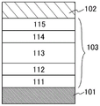


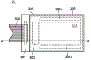


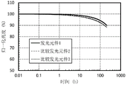


Classifications
-
- C—CHEMISTRY; METALLURGY
- C07—ORGANIC CHEMISTRY
- C07D—HETEROCYCLIC COMPOUNDS
- C07D519/00—Heterocyclic compounds containing more than one system of two or more relevant hetero rings condensed among themselves or condensed with a common carbocyclic ring system not provided for in groups C07D453/00 or C07D455/00
-
- C—CHEMISTRY; METALLURGY
- C07—ORGANIC CHEMISTRY
- C07D—HETEROCYCLIC COMPOUNDS
- C07D491/00—Heterocyclic compounds containing in the condensed ring system both one or more rings having oxygen atoms as the only ring hetero atoms and one or more rings having nitrogen atoms as the only ring hetero atoms, not provided for by groups C07D451/00 - C07D459/00, C07D463/00, C07D477/00 or C07D489/00
- C07D491/02—Heterocyclic compounds containing in the condensed ring system both one or more rings having oxygen atoms as the only ring hetero atoms and one or more rings having nitrogen atoms as the only ring hetero atoms, not provided for by groups C07D451/00 - C07D459/00, C07D463/00, C07D477/00 or C07D489/00 in which the condensed system contains two hetero rings
- C07D491/04—Ortho-condensed systems
- C07D491/044—Ortho-condensed systems with only one oxygen atom as ring hetero atom in the oxygen-containing ring
- C07D491/048—Ortho-condensed systems with only one oxygen atom as ring hetero atom in the oxygen-containing ring the oxygen-containing ring being five-membered
-
- C—CHEMISTRY; METALLURGY
- C07—ORGANIC CHEMISTRY
- C07D—HETEROCYCLIC COMPOUNDS
- C07D495/00—Heterocyclic compounds containing in the condensed system at least one hetero ring having sulfur atoms as the only ring hetero atoms
- C07D495/02—Heterocyclic compounds containing in the condensed system at least one hetero ring having sulfur atoms as the only ring hetero atoms in which the condensed system contains two hetero rings
- C07D495/04—Ortho-condensed systems
-
- C—CHEMISTRY; METALLURGY
- C09—DYES; PAINTS; POLISHES; NATURAL RESINS; ADHESIVES; COMPOSITIONS NOT OTHERWISE PROVIDED FOR; APPLICATIONS OF MATERIALS NOT OTHERWISE PROVIDED FOR
- C09K—MATERIALS FOR MISCELLANEOUS APPLICATIONS, NOT PROVIDED FOR ELSEWHERE
- C09K11/00—Luminescent, e.g. electroluminescent, chemiluminescent materials
- C09K11/06—Luminescent, e.g. electroluminescent, chemiluminescent materials containing organic luminescent materials
-
- H—ELECTRICITY
- H10—SEMICONDUCTOR DEVICES; ELECTRIC SOLID-STATE DEVICES NOT OTHERWISE PROVIDED FOR
- H10K—ORGANIC ELECTRIC SOLID-STATE DEVICES
- H10K50/00—Organic light-emitting devices
- H10K50/10—OLEDs or polymer light-emitting diodes [PLED]
- H10K50/11—OLEDs or polymer light-emitting diodes [PLED] characterised by the electroluminescent [EL] layers
-
- H—ELECTRICITY
- H10—SEMICONDUCTOR DEVICES; ELECTRIC SOLID-STATE DEVICES NOT OTHERWISE PROVIDED FOR
- H10K—ORGANIC ELECTRIC SOLID-STATE DEVICES
- H10K59/00—Integrated devices, or assemblies of multiple devices, comprising at least one organic light-emitting element covered by group H10K50/00
-
- H—ELECTRICITY
- H10—SEMICONDUCTOR DEVICES; ELECTRIC SOLID-STATE DEVICES NOT OTHERWISE PROVIDED FOR
- H10K—ORGANIC ELECTRIC SOLID-STATE DEVICES
- H10K85/00—Organic materials used in the body or electrodes of devices covered by this subclass
- H10K85/60—Organic compounds having low molecular weight
- H10K85/649—Aromatic compounds comprising a hetero atom
- H10K85/653—Aromatic compounds comprising a hetero atom comprising only oxygen as heteroatom
-
- H—ELECTRICITY
- H10—SEMICONDUCTOR DEVICES; ELECTRIC SOLID-STATE DEVICES NOT OTHERWISE PROVIDED FOR
- H10K—ORGANIC ELECTRIC SOLID-STATE DEVICES
- H10K85/00—Organic materials used in the body or electrodes of devices covered by this subclass
- H10K85/60—Organic compounds having low molecular weight
- H10K85/649—Aromatic compounds comprising a hetero atom
- H10K85/654—Aromatic compounds comprising a hetero atom comprising only nitrogen as heteroatom
-
- H—ELECTRICITY
- H10—SEMICONDUCTOR DEVICES; ELECTRIC SOLID-STATE DEVICES NOT OTHERWISE PROVIDED FOR
- H10K—ORGANIC ELECTRIC SOLID-STATE DEVICES
- H10K85/00—Organic materials used in the body or electrodes of devices covered by this subclass
- H10K85/60—Organic compounds having low molecular weight
- H10K85/649—Aromatic compounds comprising a hetero atom
- H10K85/657—Polycyclic condensed heteroaromatic hydrocarbons
- H10K85/6572—Polycyclic condensed heteroaromatic hydrocarbons comprising only nitrogen in the heteroaromatic polycondensed ring system, e.g. phenanthroline or carbazole
-
- H—ELECTRICITY
- H10—SEMICONDUCTOR DEVICES; ELECTRIC SOLID-STATE DEVICES NOT OTHERWISE PROVIDED FOR
- H10K—ORGANIC ELECTRIC SOLID-STATE DEVICES
- H10K85/00—Organic materials used in the body or electrodes of devices covered by this subclass
- H10K85/60—Organic compounds having low molecular weight
- H10K85/649—Aromatic compounds comprising a hetero atom
- H10K85/657—Polycyclic condensed heteroaromatic hydrocarbons
- H10K85/6574—Polycyclic condensed heteroaromatic hydrocarbons comprising only oxygen in the heteroaromatic polycondensed ring system, e.g. cumarine dyes
-
- H—ELECTRICITY
- H10—SEMICONDUCTOR DEVICES; ELECTRIC SOLID-STATE DEVICES NOT OTHERWISE PROVIDED FOR
- H10K—ORGANIC ELECTRIC SOLID-STATE DEVICES
- H10K85/00—Organic materials used in the body or electrodes of devices covered by this subclass
- H10K85/60—Organic compounds having low molecular weight
- H10K85/649—Aromatic compounds comprising a hetero atom
- H10K85/657—Polycyclic condensed heteroaromatic hydrocarbons
- H10K85/6576—Polycyclic condensed heteroaromatic hydrocarbons comprising only sulfur in the heteroaromatic polycondensed ring system, e.g. benzothiophene
-
- H—ELECTRICITY
- H10—SEMICONDUCTOR DEVICES; ELECTRIC SOLID-STATE DEVICES NOT OTHERWISE PROVIDED FOR
- H10K—ORGANIC ELECTRIC SOLID-STATE DEVICES
- H10K2101/00—Properties of the organic materials covered by group H10K85/00
- H10K2101/10—Triplet emission
-
- H—ELECTRICITY
- H10—SEMICONDUCTOR DEVICES; ELECTRIC SOLID-STATE DEVICES NOT OTHERWISE PROVIDED FOR
- H10K—ORGANIC ELECTRIC SOLID-STATE DEVICES
- H10K50/00—Organic light-emitting devices
- H10K50/10—OLEDs or polymer light-emitting diodes [PLED]
- H10K50/11—OLEDs or polymer light-emitting diodes [PLED] characterised by the electroluminescent [EL] layers
- H10K50/125—OLEDs or polymer light-emitting diodes [PLED] characterised by the electroluminescent [EL] layers specially adapted for multicolour light emission, e.g. for emitting white light
- H10K50/13—OLEDs or polymer light-emitting diodes [PLED] characterised by the electroluminescent [EL] layers specially adapted for multicolour light emission, e.g. for emitting white light comprising stacked EL layers within one EL unit
-
- H—ELECTRICITY
- H10—SEMICONDUCTOR DEVICES; ELECTRIC SOLID-STATE DEVICES NOT OTHERWISE PROVIDED FOR
- H10K—ORGANIC ELECTRIC SOLID-STATE DEVICES
- H10K85/00—Organic materials used in the body or electrodes of devices covered by this subclass
- H10K85/30—Coordination compounds
- H10K85/341—Transition metal complexes, e.g. Ru(II)polypyridine complexes
- H10K85/342—Transition metal complexes, e.g. Ru(II)polypyridine complexes comprising iridium
Abstract
A benzofuran pyrimidine derivative or benzothienopyrimidine derivative is provided as a novel organic compound. The present invention is an organic compound represented by the following general formula (G1). In the general formula (G1), Q represents oxygen or sulfur. A is a group having 12 to 100 carbon atoms in total, and has a heteroaromatic ring containing a benzene ring, a naphthalene ring, a fluorene ring, a phenanthrene ring, a triphenylene ring, a dibenzothiophene ring, a heteroaromatic ring containing a dibenzofuran ring, a heteroaromatic ring containing a carbazole ringAny one or more of the heteroaromatic ring, the benzimidazole ring, and the triphenylamine structure.
Description
Technical Field
One embodiment of the present invention relates to an organic compound, a light-emitting element, a light-emitting device, an electronic device, and a lighting device. One embodiment of the present invention is not limited to the above-described technical field. That is, one embodiment of the present invention relates to an object, a method, a manufacturing method, or a driving method. In addition, one embodiment of the present invention relates to a process (process), a machine (machine), a product (manufacture), or a composition (machine). Specifically, a semiconductor device, a display device, a liquid crystal display device, and the like can be given as examples.
Background
Since a light-emitting element (also referred to as an organic EL element) including an EL layer between a pair of electrodes has characteristics such as thinness, lightness in weight, high-speed response to an input signal, and low power consumption, a display using the light-emitting element is expected to be used as a next-generation flat panel display.
In the light-emitting element, when a voltage is applied between a pair of electrodes, electrons and holes injected from the respective electrodes are recombined in the EL layer, and a light-emitting substance (organic compound) included in the EL layer is brought into an excited state, and light is emitted when the excited state returns to a ground state. Further, the excited state may be of the singlet stateExcited state (S)*) And triplet excited state (T)*) In this case, light emission from a singlet excited state is referred to as fluorescence, and light emission from a triplet excited state is referred to as phosphorescence. In addition, in the light-emitting element, the statistical generation ratio of the singlet excited state and the triplet excited state is considered to be S*:T*1: 3. an emission spectrum obtained from a light-emitting substance is peculiar to the light-emitting substance, and a light-emitting element which emits various light-emitting colors can be obtained by using different kinds of organic compounds as the light-emitting substance.
In order to improve the element characteristics of such a light-emitting element, improvement of the element structure, development of materials, and the like have been actively performed (for example, see patent document 1).
[ Prior Art document ]
[ patent document ]
[ patent document 1] Japanese patent application laid-open No. 2010-182699
Disclosure of Invention
Technical problem to be solved by the invention
Accordingly, one embodiment of the present invention provides a novel organic compound. In addition, another embodiment of the present invention provides a benzofuran pyrimidine derivative or benzothienopyrimidine derivative which is a novel organic compound. In addition, one embodiment of the present invention provides a novel organic compound which can be used for a light-emitting element. In addition, one embodiment of the present invention provides a novel organic compound which can be used for an EL layer of a light-emitting element. In addition, one embodiment of the present invention provides a novel light-emitting element with high reliability using the novel organic compound of one embodiment of the present invention. In addition, one embodiment of the present invention provides a novel light-emitting device, a novel electronic device, or a novel lighting device. Note that the description of these objects does not hinder the existence of other objects. Note that one mode of the present invention is not required to achieve all the above-described objects. Note that, the objects other than the above-described object are obvious from the description of the specification, the drawings, the claims, and the like, and the objects other than the above-described object can be obtained from the description of the specification, the drawings, the claims, and the like.
Means for solving the problems
One embodiment of the present invention is a benzofuran pyrimidine derivative or benzothienopyrimidine derivative, and is an organic compound represented by the following general formula (G1). Further, the compound has a structure in which an unsubstituted phenyl group is bonded to the 8-position of a benzofuropyrimidine skeleton or a benzothienopyrimidine skeleton, as represented by the following general formula (G1).
[ chemical formula 1]

In the above general formula (G1), Q represents oxygen or sulfur. Further, a is a group having 12 to 100 total carbon atoms, and has any one or more of a heteroaromatic ring including a benzene ring, a naphthalene ring, a fluorene ring, a phenanthrene ring, a triphenylene ring, a dibenzothiophene ring, a heteroaromatic ring including a dibenzofuran ring, a heteroaromatic ring including a carbazole ring, a benzimidazole ring, and a triphenylamine structure. Furthermore, R1Represents hydrogen, an alkyl group having 1 to 6 carbon atoms, a substituted or unsubstituted monocyclic saturated hydrocarbon having 5 to 7 carbon atoms, a substituted or unsubstituted polycyclic saturated hydrocarbon having 7 to 10 carbon atoms, a substituted or unsubstituted aryl group having 6 to 13 carbon atoms, or a substituted or unsubstituted heteroaryl group having 3 to 12 carbon atoms.
In another embodiment of the present invention, the compound is a benzofuran pyrimidine derivative or benzothienopyrimidine derivative, and is an organic compound represented by the following general formula (G2). Further, as represented by the following general formula (G2), a compound having an unsubstituted phenyl group bonded to the 8-position of a benzofuropyrimidine skeleton or a benzothienopyrimidine skeleton.
[ chemical formula 2]

In the above general formula (G2), Q represents oxygen or sulfur. α represents a substituted or unsubstituted phenylene group, and n represents an integer of 0 to 4. In addition, HtuniIndicates that the compound has hole-transporting propertyThe skeleton of (2). R1Represents hydrogen, an alkyl group having 1 to 6 carbon atoms, a substituted or unsubstituted monocyclic saturated hydrocarbon having 5 to 7 carbon atoms, a substituted or unsubstituted polycyclic saturated hydrocarbon having 7 to 10 carbon atoms, a substituted or unsubstituted aryl group having 6 to 13 carbon atoms, or a substituted or unsubstituted heteroaryl group having 3 to 12 carbon atoms.
In another embodiment of the present invention, the compound is a benzofuran pyrimidine derivative or benzothienopyrimidine derivative, and is an organic compound represented by the following general formula (G3). Further, the compound has a structure in which an unsubstituted phenyl group is bonded to the 8-position of a benzofuropyrimidine skeleton or a benzothienopyrimidine skeleton, as represented by the following general formula (G3).
[ chemical formula 3]

In the above general formula (G3), Q represents oxygen or sulfur. HtuniRepresents a skeleton having a hole-transporting property. R1Represents hydrogen, an alkyl group having 1 to 6 carbon atoms, a substituted or unsubstituted monocyclic saturated hydrocarbon having 5 to 7 carbon atoms, a substituted or unsubstituted polycyclic saturated hydrocarbon having 7 to 10 carbon atoms, a substituted or unsubstituted aryl group having 6 to 13 carbon atoms, or a substituted or unsubstituted heteroaryl group having 3 to 12 carbon atoms.
In another embodiment of the present invention, the compound is a benzofuran pyrimidine derivative or benzothienopyrimidine derivative, and is an organic compound represented by the following general formula (G4). Further, the compound has a structure in which an unsubstituted phenyl group is bonded to the 8-position of a benzofuropyrimidine skeleton or a benzothienopyrimidine skeleton, as represented by the following general formula (G4).
[ chemical formula 4]

In the above general formula (G4), Q represents oxygen or sulfur. In addition, HtuniRepresents a skeleton having a hole-transporting property.R1Represents hydrogen, an alkyl group having 1 to 6 carbon atoms, a substituted or unsubstituted monocyclic saturated hydrocarbon having 5 to 7 carbon atoms, a substituted or unsubstituted polycyclic saturated hydrocarbon having 7 to 10 carbon atoms, a substituted or unsubstituted aryl group having 6 to 13 carbon atoms, or a substituted or unsubstituted heteroaryl group having 3 to 12 carbon atoms.
In each of the above structures, Ht in the general formulae (G2), (G3) and (G4) isuniEach independently has any one of a pyrrole ring structure, a furan ring structure and a thiophene ring structure.
In each of the above structures, Ht in the general formulae (G2), (G3) and (G4) isuniEach independently represents any one of the following general formulae (Ht-1) to (Ht-26).
[ chemical formula 5]

In the above general formulae (Ht-1) to (Ht-26), Q represents oxygen or sulfur. R2To R71Each represents a substituent of 1 to 4, and each independently represents any of hydrogen, an alkyl group having 1 to 6 carbon atoms, and a substituted or unsubstituted phenyl group. Ar (Ar)1Represents a substituted or unsubstituted aryl group having 6 to 13 carbon atoms.
In addition, another embodiment of the present invention is an organic compound represented by any one of structural formulae (100), (101), (102), (117), and (200).
[ chemical formula 6]

Another embodiment of the present invention is a light-emitting element using the organic compound according to one embodiment of the present invention. In addition, a light-emitting element including not only the above-described organic compound but also a guest material is included in the scope of the present invention.
Another embodiment of the present invention is a light-emitting element including the organic compound according to one embodiment of the present invention. Further, a light-emitting element in which an organic compound according to one embodiment of the present invention is used for an EL layer between a pair of electrodes and a light-emitting layer in the EL layer is also included in the scope of the present invention. In addition, the present invention includes a light-emitting element including a layer which is in contact with an electrode and includes an organic compound (for example, a cap layer) in addition to the light-emitting element described above. A light-emitting device including not only a light-emitting element but also a transistor, a substrate, and the like is also included in the scope of the invention. Further, an electronic device and a lighting device including a microphone, a camera, an operation button, an external connection portion, a housing, a cover, a support base, a speaker, and the like, in addition to the light-emitting device are also included in the scope of the invention.
In addition, one embodiment of the present invention includes not only a light-emitting device including a light-emitting element but also a lighting device including a light-emitting device. Therefore, the light-emitting device in this specification refers to an image display device or a light source (including a lighting device). In addition, the light-emitting device further includes the following modules: the light emitting device is mounted with a module of a connector such as FPC (Flexible printed circuit) or TCP (Tape Carrier Package); a module with a printed circuit board arranged at the end of the TCP; or a module in which an IC (integrated circuit) is directly mounted to a light-emitting element by a COG (Chip On Glass) method.
Effects of the invention
One embodiment of the present invention can provide a novel organic compound. In addition, one embodiment of the present invention can provide a benzofuran pyrimidine derivative or benzothienopyrimidine derivative which is a novel organic compound. One embodiment of the present invention can provide a novel organic compound which can be used for a light-emitting element. In addition, one embodiment of the present invention can provide a novel organic compound which can be used for an EL layer of a light-emitting element. In addition, one embodiment of the present invention can provide a novel light-emitting element with high reliability using the novel organic compound of one embodiment of the present invention. In addition, one embodiment of the present invention provides a novel light-emitting device, a novel electronic device, or a novel lighting device.
Brief description of the drawings
Fig. 1 is a diagram illustrating a structure of a light-emitting element.
FIG. 2 is a diagram illustrating a light-emitting device.
FIG. 3 is a diagram illustrating a light-emitting device.
Fig. 4 illustrates a diagram of an electronic device.
Fig. 5 illustrates a diagram of an electronic device.
FIG. 6 is a view illustrating an automobile.
Fig. 7 illustrates a view of the lighting device.
[ FIG. 8]]Of an organic compound represented by the formula (100)1H-NMR spectrum.
[ FIG. 9] ultraviolet and visible absorption spectra and emission spectra of an organic compound represented by the structural formula (100).
[ FIG. 10]]Of an organic compound represented by the formula (101)1H-NMR spectrum.
[ FIG. 11] ultraviolet and visible absorption spectra and emission spectra of an organic compound represented by the structural formula (101).
[ FIG. 12] A]Of an organic compound represented by the formula (102)1H-NMR spectrum.
[ FIG. 13]]Of an organic compound represented by the formula (200)1H-NMR spectrum.
FIG. 14 is a diagram illustrating a light-emitting element.
Fig. 15 is a graph showing current density-luminance characteristics of the light-emitting element 1, the comparative light-emitting element 2, and the comparative light-emitting element 3.
Fig. 16 is a graph showing voltage-luminance characteristics of the light-emitting element 1, the comparative light-emitting element 2, and the comparative light-emitting element 3.
Fig. 17 is a graph showing luminance-current efficiency characteristics of the light-emitting element 1, the comparative light-emitting element 2, and the comparative light-emitting element 3.
Fig. 18 shows voltage-current characteristics of the light-emitting element 1, the comparative light-emitting element 2, and the comparative light-emitting element 3.
Fig. 19 is a graph showing emission spectra of the light-emitting element 1, the comparative light-emitting element 2, and the comparative light-emitting element 3.
Fig. 20 is a diagram showing the reliability of the light-emitting element 1, the comparative light-emitting element 2, and the comparative light-emitting element 3.
Fig. 21 is a graph showing current density-luminance characteristics of the light-emitting elements 4 and 5.
Fig. 22 is a graph showing voltage-luminance characteristics of the light-emitting elements 4 and 5.
Fig. 23 is a graph showing luminance-current efficiency characteristics of the light-emitting elements 4 and 5.
Fig. 24 is a graph showing voltage-current characteristics of the light-emitting elements 4 and 5.
Fig. 25 is a graph showing emission spectra of the light-emitting elements 4 and 5.
Fig. 26 is a diagram showing the reliability of the light-emitting elements 4 and 5.
Fig. 27 is a graph showing current density-luminance characteristics of the light-emitting element 6, the comparative light-emitting element 7, and the comparative light-emitting element 8.
Fig. 28 is a graph showing voltage-luminance characteristics of the light-emitting element 6, the comparative light-emitting element 7, and the comparative light-emitting element 8.
Fig. 29 is a graph showing luminance-current efficiency characteristics of the light-emitting element 6, the comparative light-emitting element 7, and the comparative light-emitting element 8.
Fig. 30 is a graph showing voltage-current characteristics of the light-emitting element 6, the comparative light-emitting element 7, and the comparative light-emitting element 8.
Fig. 31 is a graph showing emission spectra of the light-emitting element 6, the comparative light-emitting element 7, and the comparative light-emitting element 8.
Fig. 32 is a diagram showing the reliability of the light-emitting element 6, the comparative light-emitting element 7, and the comparative light-emitting element 8.
[ FIG. 33]]Of an organic compound represented by the formula (117)1H-NMR spectrum.
Fig. 34 shows a current density-luminance characteristic of the light-emitting element 9.
Fig. 35 is a graph showing voltage-luminance characteristics of the light-emitting element 9.
Fig. 36 shows a graph of luminance-current efficiency characteristics of the light-emitting element 9.
Fig. 37 shows a voltage-current characteristic of the light-emitting element 9.
Fig. 38 is a graph showing an emission spectrum of the light-emitting element 9.
Modes for carrying out the invention
Embodiments of the present invention will be described below in detail with reference to the accompanying drawings. Note that the present invention is not limited to the following description, and the mode and the details thereof may be changed into various forms without departing from the spirit and the scope of the present invention. Therefore, the present invention should not be construed as being limited to the description of the embodiments shown below.
For convenience of understanding, the positions, sizes, ranges, and the like of the respective components shown in the drawings and the like do not indicate actual positions, sizes, ranges, and the like. Accordingly, the disclosed invention is not necessarily limited to the positions, sizes, ranges, etc., disclosed in the drawings and the like.
Note that in this specification and the like, when the structure of the invention is described with reference to the drawings, symbols indicating the same parts may be used in common in different drawings.
(embodiment mode 1)
In this embodiment, an organic compound according to an embodiment of the invention will be described. Note that the organic compound according to one embodiment of the present invention is a benzofuropyrimidine derivative or benzothienopyrimidine derivative represented by the following general formula (G1). As shown by the following general formula (G1), the organic compound according to one embodiment of the present invention has a structure in which an unsubstituted phenyl group is bonded to the 8-position of a benzofuropyrimidine skeleton or benzothienopyrimidine skeleton.
[ chemical formula 7]

In the general formula (G1), Q represents oxygen or sulfur. Further, a is a group having 12 to 100 total carbon atoms, and has any one or more of a heteroaromatic ring including a benzene ring, a naphthalene ring, a fluorene ring, a phenanthrene ring, a triphenylene ring, a dibenzothiophene ring, a heteroaromatic ring including a dibenzofuran ring, a heteroaromatic ring including a carbazole ring, a benzimidazole ring, and a triphenylamine structure. Furthermore, R1Represents hydrogen, an alkyl group having 1 to 6 carbon atoms, a substituted or unsubstituted monocyclic saturated hydrocarbon having 5 to 7 carbon atoms, a substituted or unsubstituted polycyclic saturated hydrocarbon having 7 to 10 carbon atoms, a substituted or unsubstituted aryl group having 6 to 13 carbon atoms, or a substituted or unsubstituted heteroaryl group having 3 to 12 carbon atoms.
Another embodiment of the present invention is an organic compound represented by the following general formula (G2).
[ chemical formula 8]

In the above general formula (G2), Q represents oxygen or sulfur. α represents a substituted or unsubstituted phenylene group, and n represents an integer of 0 to 4. In addition, HtuniRepresents a skeleton having a hole-transporting property. R1Represents hydrogen, an alkyl group having 1 to 6 carbon atoms, a substituted or unsubstituted monocyclic saturated hydrocarbon having 5 to 7 carbon atoms, a substituted or unsubstituted polycyclic saturated hydrocarbon having 7 to 10 carbon atoms, a substituted or unsubstituted aryl group having 6 to 13 carbon atoms, or a substituted or unsubstituted heteroaryl group having 3 to 12 carbon atoms.
Another embodiment of the present invention is an organic compound represented by the following general formula (G3).
[ chemical formula 9]

In the above general formula (G3), Q represents oxygen or sulfur. In addition, HtuniRepresents a skeleton having a hole-transporting property. R1Represents hydrogen, an alkyl group having 1 to 6 carbon atoms, a substituted or unsubstituted monocyclic saturated hydrocarbon having 5 to 7 carbon atoms, a substituted or unsubstituted polycyclic saturated hydrocarbon having 7 to 10 carbon atoms, a substituted or unsubstituted aryl group having 6 to 13 carbon atoms, or a substituted or unsubstituted heteroaryl group having 3 to 12 carbon atoms.
Another embodiment of the present invention is an organic compound represented by the following general formula (G4).
[ chemical formula 10]

In the above general formula (G4), Q represents oxygen or sulfur. In addition, HtuniRepresents a skeleton having a hole-transporting property. R1Represents hydrogen, an alkyl group having 1 to 6 carbon atoms, a substituted or unsubstituted monocyclic saturated hydrocarbon having 5 to 7 carbon atoms, a substituted or unsubstituted polycyclic saturated hydrocarbon having 7 to 10 carbon atoms, a substituted or unsubstituted aryl group having 6 to 13 carbon atoms, or a substituted or unsubstituted heteroaryl group having 3 to 12 carbon atoms.
Furthermore, Ht in the above general formulae (G2), (G3) and (G4)uniEach independently has any one of a pyrrole ring structure, a furan ring structure and a thiophene ring structure.
Furthermore, Ht in the above general formulae (G2), (G3) and (G4)uniEach independently represents any one of the following general formulae (Ht-1) to (Ht-26).
[ chemical formula 11]

In the above general formulae (Ht-1) to (Ht-26), Q represents oxygen or sulfur. R2To R71Each represents a substituent of 1 to 4, and each independently represents any of hydrogen, an alkyl group having 1 to 6 carbon atoms, and a substituted or unsubstituted phenyl group. Ar (Ar)1Represents a substituted or unsubstituted aryl group having 6 to 13 carbon atoms.
When the substituted or unsubstituted monocyclic saturated hydrocarbon having 5 to 7 carbon atoms, the substituted or unsubstituted polycyclic saturated hydrocarbon having 7 to 10 carbon atoms, the substituted or unsubstituted aryl group having 6 to 13 carbon atoms, the substituted or unsubstituted heteroaryl group having 3 to 12 carbon atoms, or the substituted or unsubstituted phenylene group in the above general formulae (G1), (G2), (G3), and (G4) has a substituent, examples of the substituent include: an alkyl group having 1 to 7 carbon atoms such as a methyl group, an ethyl group, a propyl group, an isopropyl group, a butyl group, an isobutyl group, a sec-butyl group, a tert-butyl group, a pentyl group, and a hexyl group; cycloalkyl groups having 5 to 7 carbon atoms such as cyclopentyl, cyclohexyl, cycloheptyl, 8,9, 10-trinononyl and the like; and aryl groups having 6 to 12 carbon atoms such as phenyl, naphthyl, and biphenyl.
R in the above general formulae (G1), (G2), (G3) and (G4)1Specific examples of the monocyclic saturated hydrocarbon having 5 to 7 carbon atoms include cyclopentyl, cyclohexyl, 1-methylcyclohexyl, cycloheptyl, and the like.
R in the above general formulae (G1), (G2), (G3) and (G4)1Specific examples of the polycyclic saturated hydrocarbon having 7 to 10 carbon atoms include norbornyl, adamantyl, decahydronaphthyl, tricyclodecanyl and the like.
R in the above general formulae (G1), (G2), (G3) and (G4)1Specific examples of the aryl group having 6 to 13 carbon atoms include phenyl, o-tolyl, m-tolyl, p-tolyl, mesityl, o-biphenyl, m-biphenyl, p-biphenylyl, 1-naphthyl, 2-naphthyl, and fluorenyl groups.
R in the above general formulae (G1), (G2), (G3) and (G4)1Specific examples of the alkyl group having 1 to 6 carbon atoms include methyl, ethyl, propyl, isopropyl, butyl, sec-butyl, isobutyl, tert-butyl, pentyl, isopentyl, sec-pentyl, tert-pentyl, neopentyl, hexyl, isohexyl, 3-methylpentyl, 2-ethylbutyl, 1, 2-dimethylbutyl, and 2, 3-dimethylbutyl.
R in the above general formulae (G1), (G2), (G3) and (G4)1Specific examples of the heteroaryl group having 3 to 12 carbon atoms include triazinyl, pyrazinyl, pyrimidinyl, pyridyl, quinolyl, isoquinolyl, benzothienyl, benzofuranyl, indolyl, dibenzothienyl, dibenzofuranyl, carbazolyl and the like.
Because of R in the above general formulae (G1), (G2), (G3) and (G4)1Has the advantages ofSpecifically, the organic compound according to one embodiment of the present invention has a high T1 level.
Next, a specific structural formula of the organic compound according to one embodiment of the present invention is shown below. Note that the present invention is not limited thereto.
[ chemical formula 12]

[ chemical formula 13]

[ chemical formula 14]

Note that the organic compounds represented by the structural formulae (100) to (123), (200) to (206) described above are one example of the organic compound represented by the general formula (G1) described above, but the organic compound of one embodiment of the present invention is not limited thereto.
Next, a method for synthesizing a benzofuropyrimidine derivative or benzothienopyrimidine derivative represented by the following general formula (G1) according to one embodiment of the present invention will be described.
[ chemical formula 15]

In the general formula (G1), Q represents oxygen or sulfur. Further, a is a group having 12 to 100 total carbon atoms, and has any one or more of a heteroaromatic ring including a benzene ring, a naphthalene ring, a fluorene ring, a phenanthrene ring, a triphenylene ring, a dibenzothiophene ring, a heteroaromatic ring including a dibenzofuran ring, a heteroaromatic ring including a carbazole ring, a benzimidazole ring, and a triphenylamine structure. Furthermore, R1Represents hydrogen and the number of carbon atoms is1 to 6 alkyl groups, substituted or unsubstituted monocyclic saturated hydrocarbons having 5 to 7 carbon atoms, substituted or unsubstituted polycyclic saturated hydrocarbons having 7 to 10 carbon atoms, substituted or unsubstituted aryl groups having 6 to 13 carbon atoms, or substituted or unsubstituted heteroaryl groups having 3 to 12 carbon atoms.
Method for synthesizing organic Compound represented by general formula (G1)
Various reactions can be used for the synthesis of the organic compound represented by the above general formula (G1), and for example, the organic compound represented by the general formula (G1) can be synthesized by a simple method shown in the following synthetic scheme.
As shown in the following synthesis scheme (P1), an organic compound represented by the general formula (G1) can be obtained by reacting a halogen compound (a1) having a benzofuropyrimidine skeleton or benzothienopyrimidine skeleton substituted with a phenyl group at the 8-position with a boronic acid compound (a2) of a.
[ chemical formula 16]

In the above synthesis scheme (P1), X represents halogen and Q represents oxygen or sulfur. Further, a is a group having 12 to 100 total carbon atoms, and has any one or more of a heteroaromatic ring including a benzene ring, a naphthalene ring, a fluorene ring, a phenanthrene ring, a triphenylene ring, a dibenzothiophene ring, a heteroaromatic ring including a dibenzofuran ring, a heteroaromatic ring including a carbazole ring, a benzimidazole ring, and a triphenylamine structure. Furthermore, R1Represents hydrogen, an alkyl group having 1 to 6 carbon atoms, a substituted or unsubstituted monocyclic saturated hydrocarbon having 5 to 7 carbon atoms, a substituted or unsubstituted polycyclic saturated hydrocarbon having 7 to 10 carbon atoms, a substituted or unsubstituted aryl group having 6 to 13 carbon atoms, or a substituted or unsubstituted heteroaryl group having 3 to 12 carbon atoms.
As shown in the following synthesis scheme (P2), a dihalogen compound (B1) having a benzofuropyrimidine skeleton or benzothienopyrimidine skeleton is reacted with a boric acid compound (a2) of a, and an intermediate (B2) is reacted with a boric acid compound (B3), whereby an organic compound represented by general formula (G1) can be obtained.
[ chemical formula 17]

In the above synthesis scheme (P2), X represents halogen and Q represents oxygen or sulfur. Further, a is a group having 12 to 100 total carbon atoms, and has any one or more of a heteroaromatic ring including a benzene ring, a naphthalene ring, a fluorene ring, a phenanthrene ring, a triphenylene ring, a dibenzothiophene ring, a heteroaromatic ring including a dibenzofuran ring, a heteroaromatic ring including a carbazole ring, a benzimidazole ring, and a triphenylamine structure. Furthermore, R1Represents hydrogen, an alkyl group having 1 to 6 carbon atoms, a substituted or unsubstituted monocyclic saturated hydrocarbon having 5 to 7 carbon atoms, a substituted or unsubstituted polycyclic saturated hydrocarbon having 7 to 10 carbon atoms, a substituted or unsubstituted aryl group having 6 to 13 carbon atoms, or a substituted or unsubstituted heteroaryl group having 3 to 12 carbon atoms. In addition, B1Represents boric acid, boric acid ester, or cyclic triol borate. Further, as the cyclic triol borate, a potassium salt or a sodium salt may be used in addition to a lithium salt.
As shown in the following synthetic scheme (P3), a trihalo compound (C1) having a benzofuropyrimidine skeleton or benzothienopyrimidine skeleton is reacted with a boric acid compound (A2) of A, and an intermediate (C2) and R are reacted1The boronic acid compound (C3) is reacted, and the intermediate (C4) is reacted with the phenyl boronic acid compound (B3), whereby the organic compound represented by the general formula (G1) can be obtained.
[ chemical formula 18]

In the above synthesis scheme (P3), X represents halogen and Q represents oxygen or sulfur. Further, A is a group having 12 to 100 carbon atoms in total, and has a heteroaromatic ring containing a benzene ring, a naphthalene ring, a fluorene ring, a phenanthrene ring, a triphenylene ring, a dibenzothiophene ring, a heteroaromatic ring containing a dibenzofuran ring, a heteroaromatic ring containing a carbazoleAny one or more of heteroaromatic ring, benzimidazole ring and triphenylamine structure of the ring. Furthermore, R1Represents hydrogen, an alkyl group having 1 to 6 carbon atoms, a substituted or unsubstituted monocyclic saturated hydrocarbon having 5 to 7 carbon atoms, a substituted or unsubstituted polycyclic saturated hydrocarbon having 7 to 10 carbon atoms, a substituted or unsubstituted aryl group having 6 to 13 carbon atoms, or a substituted or unsubstituted heteroaryl group having 3 to 12 carbon atoms. In addition, B1Represents boric acid, boric acid ester, or cyclic triol borate. Further, as the cyclic triol borate, a potassium salt or a sodium salt may be used in addition to a lithium salt.
The halogen compound having a benzofuropyrimidine skeleton or benzothienopyrimidine skeleton substituted with a phenyl group at the 8-position (a1), the boronic acid compound of a (a2), the dihalogen compound having a benzofuropyrimidine skeleton or benzothienopyrimidine skeleton (B1), the intermediate (B2), the phenylboronic acid compound (B3), the trihalogen compound having a benzofuropyrimidine skeleton or benzothienopyrimidine skeleton (C1), the intermediate (C2), R used in the above-mentioned synthesis schemes (P1), (P2) and (P3), the intermediate (B2), the phenylboronic acid compound (B3), the trihalogen compound having a benzofuropyrimidine skeleton or benzothienopyrimidine skeleton (C11The boronic acid compound (C3) and the intermediate (C4) are commercially available in many kinds or can be synthesized, and thus, a variety of benzofuropyrimidine derivatives or benzothienopyrimidine derivatives represented by the general formula (G1) can be synthesized. Therefore, the organic compound according to one embodiment of the present invention is characterized by being abundant in its kind.
Although an example of the organic compound and the method for synthesizing the same according to one embodiment of the present invention has been described above, the present invention is not limited to this, and may be synthesized by another synthesis method.
The structure described in this embodiment can be used in combination with the structures described in the other embodiments as appropriate.
(embodiment mode 2)
In this embodiment, a light-emitting element using the organic compound described in embodiment 1 will be described with reference to fig. 1.
Basic Structure of light emitting element
First, a basic structure of the light-emitting element is described. Fig. 1A shows an example of a light-emitting element having an EL layer including a light-emitting layer between a pair of electrodes. Specifically, the light-emitting element has a structure in which the EL layer 103 is sandwiched between the first electrode 101 and the second electrode 102.
Fig. 1B shows an example of a light-emitting element having a stacked-layer structure (series structure) in which a plurality of (two layers in fig. 1B) EL layers (103a and 103B) are provided between a pair of electrodes and a charge generation layer 104 is provided between the EL layers. The light-emitting element having the series structure can realize a light-emitting device which can be driven at low voltage and has low power consumption.
The charge generation layer 104 has the following functions: when a voltage is applied to the first electrode 101 and the second electrode 102, electrons are injected into one EL layer (103a or 103b) and holes are injected into the other EL layer (103b or 103 a). Thus, in fig. 1B, when a voltage is applied so that the potential of the first electrode 101 is higher than that of the second electrode 102, the charge generation layer 104 injects electrons into the EL layer 103a and injects holes into the EL layer 103B.
In addition, from the viewpoint of light extraction efficiency, the charge generation layer 104 preferably has a light-transmitting property with respect to visible light (specifically, the visible light transmittance of the charge generation layer 104 is 40% or more). In addition, the charge generation layer 104 can function even if it has lower conductivity than the first electrode 101 or the second electrode 102.
Fig. 1C shows an example of a case where the EL layer 103 shown in fig. 1A (the same applies to a case where the EL layers (103a and 103B) in fig. 1B have a stacked structure) has a stacked structure. Note that in this case, the first electrode 101 is used as an anode. The EL layer 103 has a structure in which a hole injection layer 111, a hole transport layer 112, a light-emitting layer 113, an electron transport layer 114, and an electron injection layer 115 are sequentially stacked over the first electrode 101. In the case where a plurality of EL layers are provided as in the series structure shown in fig. 1B, the EL layers are also stacked from the anode side as described above. In addition, when the first electrode 101 is a cathode and the second electrode 102 is an anode, the order of stacking the EL layers is reversed.
The light-emitting layer 113 in the EL layers (103, 103a, and 103b) can be formed by appropriately combining a light-emitting substance and a plurality of substances, and can obtain fluorescent light emission and phosphorescent light emission which show desired light emission colors. The light-emitting layer 113 may have a stacked structure with different emission colors. In this case, different materials may be used for the light-emitting substance and the other substance used in each of the stacked light-emitting layers. Further, a structure in which different emission colors are obtained from the plurality of EL layers (103a and 103B) shown in fig. 1B may be employed. In this case, different materials may be used for the light-emitting substance and the other substance used in each light-emitting layer.
In addition, in the light-emitting element according to one embodiment of the present invention, light obtained in the EL layers (103, 103a, 103b) can be resonated between electrodes, and the obtained light can be enhanced. For example, in fig. 1C, by making the first electrode 101 a reflective electrode and the second electrode 102 a semi-transmissive-semi-reflective electrode, an optical microcavity resonator (microcavity) structure is formed, whereby light obtained from the EL layer 103 can be enhanced.
When the first electrode 101 of the light-emitting element is a reflective electrode having a stacked structure of a conductive material having reflectivity and a conductive material having translucency (transparent conductive film), optical adjustment can be performed by controlling the thickness of the transparent conductive film. Specifically, the adjustment is preferably performed as follows: when the wavelength of light obtained from the light-emitting layer 113 is λ, the distance between the first electrode 101 and the second electrode 102 is about m λ/2 (note that m is a natural number).
In order to amplify the desired light (wavelength: λ) obtained from the light-emitting layer 113, it is preferable to adjust the following: the optical distance from the first electrode 101 to the region (light-emitting region) of the light-emitting layer 113 where desired light can be obtained and the optical distance from the second electrode 102 to the region (light-emitting region) of the light-emitting layer 113 where desired light can be obtained are both around (2m '+ 1) λ/4 (note that m' is a natural number). Note that the "light-emitting region" described here refers to a recombination region of holes and electrons in the light-emitting layer 113.
By performing the optical adjustment, the spectrum of the specific monochromatic light obtained from the light-emitting layer 113 can be narrowed, and light emission with good color purity can be obtained.
Note that in the above case, strictly speaking, the optical distance between the first electrode 101 and the second electrode 102 can be said to be the total thickness from the reflective region in the first electrode 101 to the reflective region in the second electrode 102. However, since it is difficult to accurately determine the position of the reflective region in the first electrode 101 or the second electrode 102, the above-described effects can be sufficiently obtained by assuming that any position of the first electrode 101 and the second electrode 102 is the reflective region. In addition, strictly speaking, the optical distance between the first electrode 101 and the light-emitting layer that can obtain desired light can be said to be the optical distance between the reflective region in the first electrode 101 and the light-emitting region in the light-emitting layer that can obtain desired light. However, since it is difficult to accurately determine the position of the reflective region in the first electrode 101 or the light-emitting region in the light-emitting layer from which desired light can be obtained, the above-described effects can be sufficiently obtained by assuming that an arbitrary position in the first electrode 101 is the reflective region and an arbitrary position in the light-emitting layer from which desired light can be obtained is the light-emitting region.
In the case where the light emitting element shown in fig. 1C has a microcavity structure, light of different wavelengths (monochromatic light) can be extracted even with the same EL layer. Thus, separate coatings (e.g., R, G, B) are not required to obtain different emission colors. Thereby, high resolution can be achieved. In addition, it may be combined with a colored layer (color filter). Further, the emission intensity in the front direction of the specific wavelength can be enhanced, and low power consumption can be achieved.
The light-emitting element shown in fig. 1E is an example of the light-emitting element having the series structure shown in fig. 1B, and has a structure in which three EL layers (103a, 103B, and 103c) are stacked with charge generation layers (104a and 104B) interposed therebetween, as shown in the drawing. The three EL layers (103a, 103b, 103c) include light-emitting layers (113a, 113b, 113c), respectively, and the emission colors of the light-emitting layers can be freely combined. For example, the light-emitting layers 113a and 113c may be blue, and the light-emitting layer 113b may be one of red, green, and yellow. For example, the light-emitting layers 113a and 113c may be red, and the light-emitting layer 113b may be blue, green, or yellow.
In addition, the present invention is described aboveIn the light-emitting element of one embodiment, at least one of the first electrode 101 and the second electrode 102 is a light-transmitting electrode (e.g., a transparent electrode or a semi-transmissive and semi-reflective electrode). When the electrode having light transmittance is a transparent electrode, the visible light transmittance of the transparent electrode is 40% or more. In the case where the electrode is a semi-transmissive-semi-reflective electrode, the visible light reflectance of the semi-transmissive-semi-reflective electrode is 20% or more and 80% or less, and preferably 40% or more and 70% or less. In addition, the resistivity of these electrodes is preferably 1 × 10⁻²Omega cm or less.
In the light-emitting element according to the above-described one embodiment of the present invention, when one of the first electrode 101 and the second electrode 102 is a reflective electrode (reflective electrode), the visible light reflectance of the reflective electrode is 40% or more and 100% or less, and preferably 70% or more and 100% or less. In addition, the resistivity of the electrode is preferably 1 × 10⁻²Omega cm or less.
Concrete structure and manufacturing method of light emitting element
Next, a specific structure and a manufacturing method of the light-emitting element shown in fig. 1 according to one embodiment of the present invention will be described. Here, not only a light-emitting element in which the EL layer 103 shown in fig. 1A and 1C has a single-layer structure but also a light-emitting element in which the series structure shown in fig. 1B, 1D, and 1E is included will be described. In the case where each light-emitting element shown in fig. 1 has a microcavity structure, for example, a reflective electrode may be formed as the first electrode 101 and a semi-transmissive-semi-reflective electrode may be formed as the second electrode 102. Thus, the electrode can be formed by using a desired electrode material alone or by using a plurality of desired electrode materials in a single layer or a stacked layer. After the EL layers (103, 103b) are formed, the second electrode 102 is formed by selecting the material in the same manner as described above. The electrode may be formed by a sputtering method or a vacuum deposition method.
< first electrode and second electrode >
As materials for forming the first electrode 101 and the second electrode 102, the following materials may be appropriately combined if the functions of the two electrodes can be satisfied. For example, metals, alloys, conductive compounds, mixtures thereof, and the like can be suitably used. Specific examples thereof include an In-Sn oxide (also referred to as ITO), an In-Si-Sn oxide (also referred to as ITSO), an In-Zn oxide, and an In-W-Zn oxide. In addition to the above, metals such as aluminum (Al), titanium (Ti), chromium (Cr), manganese (Mn), iron (Fe), cobalt (Co), nickel (Ni), copper (Cu), gallium (Ga), zinc (Zn), indium (In), tin (Sn), molybdenum (Mo), tantalum (Ta), tungsten (W), palladium (Pd), gold (Au), platinum (Pt), silver (Ag), yttrium (Y), neodymium (Nd), and alloys appropriately combining these metals may be mentioned. In addition to the above, elements belonging to group 1 or group 2 of the periodic table (for example, rare earth metals such as lithium (Li), cesium (Cs), calcium (Ca), strontium (Sr)), europium (Eu), ytterbium (Yb), etc., alloys in which these are appropriately combined, graphene, and the like can be used.
In the case where the light-emitting element shown in fig. 1 includes the EL layer 103 having the stacked structure shown in fig. 1C and the first electrode 101 is an anode, the hole injection layer 111 and the hole transport layer 112 of the EL layer 103 are sequentially stacked on the first electrode 101 by a vacuum evaporation method. Further, as shown in fig. 1D, when a plurality of EL layers (103a, 103b) having a stacked structure are stacked with the charge generation layer 104 interposed therebetween and the first electrode 101 is a cathode, the hole injection layer 111a and the hole transport layer 112a of the EL layer 103a are sequentially stacked on the first electrode 101 by a vacuum evaporation method, and after the EL layer 103a and the charge generation layer 104 are sequentially stacked, the hole injection layer 111b and the hole transport layer 112b of the EL layer 103b are sequentially stacked on the charge generation layer 104 in the same manner as described above.
< hole injection layer and hole transport layer >
The hole injection layers (111, 111a, 111b) are layers for injecting holes from the first electrode 101 or the charge generation layer (104) of the anode into the EL layers (103, 103a, 103b), and include a material having a high hole injection property.
Examples of the material having a high hole-injecting property include transition metal oxides such as molybdenum oxide, vanadium oxide, ruthenium oxide, tungsten oxide, and manganese oxide. In addition to the above, phthalocyanine-based compounds such as phthalocyanine (abbreviated as H) can be used2Pc), copper phthalocyanine (CuPc), and the like.
In addition, aromatic amine compounds of low-molecular compounds such as 4,4 '-tris (N, N-diphenylamino) triphenylamine (abbreviated as TDATA), 4' -tris [ N- (3-methylphenyl) -N-phenylamino ] triphenylamine (abbreviated as MTDATA), 4 '-bis [ N- (4-diphenylaminophenyl) -N-phenylamino ] biphenyl (abbreviated as DPAB), 4' -bis (N- {4- [ N '- (3-methylphenyl) -N' -phenylamino ] phenyl } -N-phenylamino) biphenyl (abbreviated as DNTPD), 1,3, 5-tris [ N- (4-diphenylaminophenyl) -N-phenylamino ] benzene (abbreviated as DPA3B), and the like can be used, 3- [ N- (9-phenylcarbazol-3-yl) -N-phenylamino ] -9-phenylcarbazole (abbreviated as PCzPCA1), 3, 6-bis [ N- (9-phenylcarbazol-3-yl) -N-phenylamino ] -9-phenylcarbazole (abbreviated as PCzPCA2), 3- [ N- (1-naphthyl) -N- (9-phenylcarbazol-3-yl) amino ] -9-phenylcarbazole (abbreviated as PCzPCN1), and the like.
In addition, high molecular compounds (oligomers, dendrimers or polymers) such as Poly (N-vinylcarbazole) (abbreviated as PVK), Poly (4-vinyltriphenylamine) (abbreviated as PVTPA), Poly [ N- (4- { N '- [4- (4-diphenylamino) phenyl ] phenyl-N' -phenylamino } phenyl) methacrylamide ] (abbreviated as PTPDMA), Poly [ N, N '-bis (4-butylphenyl) -N, N' -bis (phenyl) benzidine ] (abbreviated as Poly-TPD) and the like can be used. Alternatively, a polymer compound to which an acid is added, such as poly (3, 4-ethylenedioxythiophene)/poly (styrenesulfonic acid) (abbreviated as PEDOT/PSS) or polyaniline/poly (styrenesulfonic acid) (PANI/PSS), may also be used.
As the material having a high hole-injecting property, a composite material including a hole-transporting material and an acceptor material (electron acceptor material) may be used. In this case, electrons are extracted from the hole-transporting material by the acceptor material, holes are generated in the hole-injecting layers (111, 111a, 111b), and the holes are injected into the light-emitting layers (113, 113a, 113b) through the hole-transporting layers (112, 112a, 112 b). The hole injection layers (111, 111a, and 111b) may be formed of a single layer of a composite material including a hole-transporting material and an acceptor material (electron acceptor material), or may be formed of a stack of layers formed using a hole-transporting material and an acceptor material (electron acceptor material).
The hole transport layers (112, 112a, 112b) are layers that transport holes injected from the first electrode 101 through the hole injection layers (111, 111a, 111b) into the light emitting layers (113, 113a, 113 b). The hole-transporting layer (112, 112a, 112b) is a layer containing a hole-transporting material. As the hole-transporting material used for the hole-transporting layers (112, 112a, 112b), a material having the HOMO energy level that is the same as or close to the HOMO energy level of the hole-injecting layers (111, 111a, 111b) is particularly preferably used.
As an acceptor material for the hole injection layer (111, 111a, 111b), an oxide of a metal belonging to groups 4 to 8 in the periodic table of elements can be used. Specific examples thereof include molybdenum oxide, vanadium oxide, niobium oxide, tantalum oxide, chromium oxide, tungsten oxide, manganese oxide, and rhenium oxide. Molybdenum oxide is particularly preferably used because it is also stable in the atmosphere, has low hygroscopicity, and is easy to handle. In addition to the above, examples include organic acceptors such as quinodimethane derivatives, tetrachlorobenzoquinone derivatives, and hexaazatriphenylene derivatives. Examples of the compound having an electron-withdrawing group (halogen group or cyano group) include 7, 7, 8, 8-tetracyano-2, 3,5, 6-tetrafluoroquinodimethane (abbreviated as F)4TCNQ), chloranil, 2,3, 6, 7, 10, 11-hexacyan-1, 4, 5, 8,9, 12-hexaazatriphenylene (abbreviation: HAT-CN), 1,3,4, 5, 7, 8-hexafluorotetracyano (hexafluoroacetonitrile) -naphthoquinone dimethane (naphthoquinodimethane) (abbreviation: F6-TCNNQ), and the like. In particular, a compound in which a condensed aromatic ring having a plurality of hetero atoms such as HAT-CN is bonded to an electron-withdrawing group is preferable because it is thermally stable. Further, [ 3] comprising an electron-withdrawing group (particularly, a halogen group such as a fluoro group, a cyano group)]The axine derivative is particularly preferable because it has a very high electron-accepting property. Specifically, there may be mentioned: alpha, alpha' -1,2, 3-cyclopropane triylidene tris [ 4-cyano-2, 3,5, 6-tetrafluorophenylacetonitrile]Alpha, alpha' -1,2, 3-cyclopropane triylidenetris [2, 6-dichloro-3, 5-difluoro-4- (trifluoromethyl) benzeneacetonitrile]Alpha, alpha' -1,2, 3-cyclopropane triylidene tris [2, 3,4, 5, 6-pentafluorophenylacetonitrile]And the like.
The hole-transporting material used for the hole-injecting layers (111, 111a, 111b) and the hole-transporting layers (112, 112a, 112b) preferably has a hole-transporting property of 10-6cm2Holes above VsA species of mobility. In addition, any substance other than the above may be used as long as it has a hole-transporting property higher than an electron-transporting property.
The hole-transporting material is preferably a material having high hole-transporting property, such as a pi-electron-rich heteroaromatic compound (e.g., a carbazole derivative, a furan derivative, and a thiophene derivative) or an aromatic amine (a compound having an aromatic amine skeleton).
Examples of the carbazole derivative (compound having a carbazole skeleton) include a biscarbazole derivative (for example, 3, 3' -biscarbazole derivative), an aromatic amine having a carbazole group, and the like.
Specific examples of the bicarbazole derivative (for example, 3,3 '-bicarbazole derivative) include 3, 3' -bis (9-phenyl-9H-carbazole) (PCCP), 9 '-bis (1, 1' -biphenyl-4-yl) -3,3 '-bi-9H-carbazole, 9' -bis (1,1 '-biphenyl-3-yl) -3, 3' -bi-9H-carbazole, 9- (1,1 '-biphenyl-3-yl) -9' - (1,1 '-biphenyl-4-yl) -9H, 9' H-3,3 '-bicarbazole (mBPCCBP), 9- (2-naphthyl) -9' -phenyl-9H, 9 'H-3, 3' -bicarbazole (abbreviated as. beta. NCCP), and the like.
Specific examples of the aromatic amine having a carbazole group include 4-phenyl-4 '- (9-phenyl-9H-carbazol-3-yl) triphenylamine (abbreviated to PCBA1BP), N- (4-biphenyl) -N- (9, 9-dimethyl-9H-fluoren-2-yl) -9-phenyl-9H-carbazol-3-amine (abbreviated to pcpef), N- (1, 1' -biphenyl-4-yl) -N- [4- (9-phenyl-9H-carbazol-3-yl) phenyl ] -9, 9-dimethyl-9H-fluoren-2-amine (abbreviated to PCBBiF), and 4,4' -diphenyl-4 ' - (9-phenyl-9H-carbazol-3-yl) triphenylamine (abbreviated as PCBBi1BP), 4- (1-naphthyl) -4' - (9-phenyl-9H-carbazol-3-yl) triphenylamine (abbreviated as PCBANB), 4' -bis (1-naphthyl) -4' - (9-phenyl-9H-carbazol-3-yl) triphenylamine (abbreviated as PCBNBB), 4-phenyldiphenyl- (9-phenyl-9H-carbazol-3-yl) amine (abbreviated as PCA1BP), N ' -bis (9-phenylcarbazol-3-yl) -N, N ' -diphenylbenzene-1, 3-diamine (PCA 2B), N ' -triphenyl-N, N ' -tris (9-phenylcarbazol-3-yl) benzene-1, 3, 5-triamine (PCA 3B), 9-dimethyl-N-phenyl-N- [4- (9-phenyl-9H-carbazol-3-yl) phenyl ] fluorene-2-amine (PCBAF), N-phenyl-N- [4- (9-phenyl-9H-carbazol-3-yl) phenyl ] spiro-9, 9 ' -bifluorene-2-amine (PCBASF), 3- [ N- (9-phenylcarbazol-3-yl) -N-phenylamino ] -9-phenylcarbazole (PCA 1), 3, 6-bis [ N- (9-phenylcarbazol-3-yl) -N-phenylamino ] -9-phenylcarbazole (abbreviation: PCzPCA2), 3- [ N- (1-naphthyl) -N- (9-phenylcarbazol-3-yl) amino ] -9-phenylcarbazole (abbreviation: PCzPCN1), 3- [ N- (4-diphenylaminophenyl) -N-phenylamino ] -9-phenylcarbazole (abbreviation: PCzDPA1), 3, 6-bis [ N- (4-diphenylaminophenyl) -N-phenylamino ] -9-phenylcarbazole (abbreviation: PCzDPA2), 3, 6-bis [ N- (4-diphenylaminophenyl) -N- (1-naphthyl) amino ] -9-phenylcarbazole (abbreviation: PCzTPN2) ) 2- [ N- (9-phenylcarbazol-3-yl) -N-phenylamino ] spiro-9, 9' -bifluorene (abbreviation: PCASF), N- [4- (9H-carbazol-9-yl) phenyl ] -N- (4-phenyl) phenylaniline (abbreviation: YGA1BP), N '-bis [4- (carbazol-9-yl) phenyl ] -N, N' -diphenyl-9, 9-dimethylfluorene-2, 7-diamine (abbreviation: YGA2F), 4',4 ″ -tris (carbazol-9-yl) triphenylamine (abbreviation: TCTA), and the like.
As the carbazole derivative, in addition to the above, examples thereof include 3- [4- (9-phenanthryl) -phenyl ] -9-phenyl-9H-carbazole (abbreviated as PCPPn), 3- [4- (1-naphthyl) -phenyl ] -9-phenyl-9H-carbazole (abbreviated as PCPN), 1, 3-bis (N-carbazolyl) benzene (abbreviated as mCP), 4' -bis (N-carbazolyl) biphenyl (abbreviated as CBP), 3, 6-bis (3, 5-diphenylphenyl) -9-phenylcarbazole (abbreviated as CZTP), 1,3, 5-tris [4- (N-carbazolyl) phenyl ] benzene (abbreviated as TCPB), 9- [4- (10-phenyl-9-anthracyl) phenyl ] -9H-carbazole (abbreviated as CZPA) and the like.
Specific examples of the thiophene derivative and furan derivative include compounds having a thiophene skeleton such as 1,3, 5-tris (dibenzothiophen-4-yl) benzene (abbreviated as DBT3P-II), 2, 8-diphenyl-4- [4- (9-phenyl-9H-fluoren-9-yl) phenyl ] dibenzothiophene (abbreviated as DBTFLP-III), 4- [4- (9-phenyl-9H-fluoren-9-yl) phenyl ] -6-phenyldibenzothiophene (abbreviated as DBTFLP-IV), 4' - (benzene-1, 3, 5-triyl) tris (dibenzofuran) (abbreviated as DBF3P-II), and 4- {3- [3- (9-phenyl-9H-fluoren-9-yl) phenyl ] benzene And compounds having a furan skeleton such as mesityl dibenzofuran (abbreviated as mmDBFFLBi-II).
Specific examples of the aromatic amine include 4,4' -bis [ N- (1-naphthyl) -N-phenylamino ] biphenyl (abbreviated as NPB or. alpha. -NPD), N ' -bis (3-methylphenyl) -N, N ' -diphenyl- [1,1 ' -biphenyl ] -4, 4' -diamine (abbreviated as TPD), 4' -bis [ N- (spiro-9, 9 ' -difluoren-2-yl) -N-phenylamino ] biphenyl (abbreviated as BSPB), 4-phenyl-4 ' - (9-phenylfluoren-9-yl) triphenylamine (abbreviated as BPAFLP), 4-phenyl-3 ' - (9-phenylfluoren-9-yl) triphenylamine (abbreviated as mBPAFLP), N- (9, 9-dimethyl-9H-fluoren-2-yl) -N- {9, 9-dimethyl-2- [ N ' -phenyl-N ' - (9, 9-dimethyl-9H-fluoren-2-yl) amino ] -9H-fluoren-7-yl } phenylamine (abbreviated: DFLADFL), N- (9, 9-dimethyl-2-diphenylamino-9H-fluoren-7-yl) diphenylamine (abbreviated: DPNF), 2- [ N- (4-diphenylaminophenyl) -N-phenylamino ] spiro-9, 9 ' -bifluorene (abbreviated: DPASF), 2, 7-bis [ N- (4-diphenylaminophenyl) -N-phenylamino ] spiro-9, 9 ' -bifluorene (abbreviated as DPA2SF), 4' -tris [ N- (1-naphthyl) -N-phenylamino ] triphenylamine (abbreviated as 1 ' -TNATA), 4' -tris (N, N-diphenylamino) triphenylamine (abbreviated as TDATA), 4' -tris [ N- (3-methylphenyl) -N-phenylamino ] triphenylamine (abbreviated as m-MTDATA), N ' -bis (p-tolyl) -N, N ' -diphenyl-p-phenylenediamine (abbreviated as DTDPPA), 4' -bis [ N- (4-diphenylaminophenyl) -N-phenylamino ] biphenyl (abbreviated as DPAB), N ' -bis {4- [ bis (3-methylphenyl) amino ] phenyl } -N, n ' -diphenyl- (1,1 ' -biphenyl) -4, 4' -diamine (abbreviated as DNTPD), 1,3, 5-tris [ N- (4-diphenylaminophenyl) -N-phenylamino ] benzene (abbreviated as DPA3B), and the like.
As the hole transporting material, a polymer compound such as Poly (N-vinylcarbazole) (abbreviated as PVK), Poly (4-vinyltriphenylamine) (abbreviated as PVTPA), Poly [ N- (4- { N '- [4- (4-diphenylamino) phenyl ] phenyl-N' -phenylamino } phenyl) methacrylamide ] (abbreviated as PTPDMA), Poly [ N, N '-bis (4-butylphenyl) -N, N' -bis (phenyl) benzidine ] (abbreviated as Poly-TPD) or the like can be used.
Note that the hole-transporting material is not limited to the above-described materials, and one or a combination of a plurality of known materials can be used as the hole-transporting material for the hole injection layers (111, 111a, 111b) and the hole transport layers (112, 112a, 112 b). The hole transport layers (112, 112a, 112b) may be formed of a plurality of layers. That is, for example, the first hole transport layer and the second hole transport layer may be stacked.
In the light-emitting element shown in fig. 1, the light-emitting layers (113, 113a) are formed on the hole transport layers (112, 112a) in the EL layers (103, 103a) by a vacuum evaporation method. In the case of the light-emitting element having the tandem structure shown in fig. 1D, after the EL layer 103a and the charge generation layer 104 are formed, the light-emitting layer 113b is formed on the hole transport layer 112b in the EL layer 103b by a vacuum evaporation method.
< light-emitting layer >
The light-emitting layers (113, 113a, 113b, 113c) are layers containing a light-emitting substance. As the light-emitting substance, a substance exhibiting a light-emitting color such as blue, violet, bluish-violet, green, yellowish green, yellow, orange, or red is suitably used. Further, by using different light-emitting substances in each of the plurality of light-emitting layers (113a, 113b, and 113c), it is possible to have a structure in which different light-emitting colors are exhibited (for example, white light can be obtained by combining light-emitting colors in a complementary color relationship). Further, a stacked structure in which one light-emitting layer includes different light-emitting substances may be employed.
The light-emitting layers (113, 113a, 113b, and 113c) may contain one or more organic compounds (host materials, etc.) in addition to the light-emitting substance (guest material). As the one or more kinds of organic compounds, one or both of the organic compound of one embodiment of the present invention, the hole-transporting material and the electron-transporting material described in this embodiment can be used.
The light-emitting substance that can be used in the light-emitting layers (113, 113a, 113b, and 113c) is not particularly limited, and a light-emitting substance that converts singlet excitation energy into light in the visible light region or a light-emitting substance that converts triplet excitation energy into light in the visible light region can be used.
Examples of the other luminescent materials include the following.
Examples of the light-emitting substance which converts a single excitation energy into light emission include substances which emit fluorescence (fluorescent materials), and examples thereof include pyrene derivatives, anthracene derivatives, triphenylene derivatives, fluorene derivatives, carbazole derivatives, dibenzothiophene derivatives, dibenzofuran derivatives, dibenzoquinoxaline derivatives, quinoxaline derivatives, pyridine derivatives, pyrimidine derivatives, phenanthrene derivatives, and naphthalene derivatives. In particular, the pyrene derivative is preferable because the luminescence quantum yield is high. Specific examples of the pyrene derivative include N, N ' -bis (3-methylphenyl) -N, N ' -bis [3- (9-phenyl-9H-fluoren-9-yl) phenyl ] pyrene-1, 6-diamine (abbreviated as 1, 6mMemFLPAPRn), N ' -diphenyl-N, N ' -bis [4- (9-phenyl-9H-fluoren-9-yl) phenyl ] pyrene-1, 6-diamine (abbreviated as 1, 6FLPAPRn), N ' -bis (dibenzofuran-2-yl) -N, N ' -diphenylpyrene-1, 6-diamine (abbreviated as 1, 6FrAPrn), N ' -bis (dibenzothiophene-2-yl) -N, n '-Diphenylpyrene-1, 6-diamine (abbreviated as 1, 6ThAPrn), N' - (pyrene-1, 6-diyl) bis [ (N-phenylbenzo [ b ] naphtho [1,2-d ] furan) -6-amine ] (abbreviated as 1, 6BnfAPrn), N '- (pyrene-1, 6-diyl) bis [ (N-phenylbenzo [ b ] naphtho [1,2-d ] furan) -8-amine ] (abbreviated as 1, 6BnfAPrn-02), N' - (pyrene-1, 6-diyl) bis [ (6, N-diphenylbenzo [ b ] naphtho [1,2-d ] furan) -8-amine ] (abbreviated as 1, 6BnfAPrn-03), and the like.
In addition to the above, 5, 6-bis [4- (10-phenyl-9-anthracenyl) phenyl ] -2, 2 '-bipyridine (abbreviated as PAP2BPy), 5, 6-bis [4' - (10-phenyl-9-anthracenyl) biphenyl-4-yl ] -2, 2 '-bipyridine (abbreviated as PAPP2BPy), N' -bis [4- (9H-carbazol-9-yl) phenyl ] -N, N '-diphenylstilbene-4, 4' -diamine (abbreviated as YGA2S), 4- (9H-carbazol-9-yl) -4'- (10-phenyl-9-anthracenyl) triphenylamine (abbreviated as YGAPA), 4- (9H-carbazol-9-yl) -4' - (9H-carbazol-9-yl) triphenylamine (abbreviated as YGAPA), 10-diphenyl-2-anthryl) triphenylamine (abbreviation: 2YGAPPA), N, 9-diphenyl-N- [4- (10-phenyl-9-anthracenyl) phenyl ] -9H-carbazol-3-amine (abbreviation: PCAPA), 4- (10-phenyl-9-anthracenyl) -4' - (9-phenyl-9H-carbazol-3-yl) triphenylamine (abbreviation: PCBAPA), 4- [4- (10-phenyl-9-anthracenyl) phenyl ] -4' - (9-phenyl-9H-carbazol-3-yl) triphenylamine (abbreviation: pcbappaba), perylene, 2, 5, 8, 11-tetra-tert-butyl perylene (abbreviation: TBP), N ″ - (2-tert-butylanthracene-9, 10-diylbis-4, 1-phenylene) bis [ N, N' -triphenyl-1, 4-phenylenediamine ] (abbreviation: DPABPA), N, 9-diphenyl-N- [4- (9, 10-diphenyl-2-anthracenyl) phenyl ] -9H-carbazol-3-amine (abbreviation: 2PCAPPA), N- [4- (9, 10-diphenyl-2-anthryl) phenyl ] -N, N' -triphenyl-1, 4-phenylenediamine (abbreviation: 2DPAPPA), and the like.
Examples of the light-emitting substance which converts triplet excitation energy into light emission include a substance which emits phosphorescence (phosphorescent material) and a Thermally Activated Delayed Fluorescence (TADF) material which exhibits Thermally activated delayed fluorescence.
Examples of the phosphorescent material include an organometallic complex, a metal complex (platinum complex), a rare earth metal complex, and the like. Such substances exhibit different emission colors (emission peaks), and are selected and used as needed.
The following can be mentioned as examples of phosphorescent materials which exhibit blue or green color and have an emission spectrum with a peak wavelength of 450nm to 570 nm.
For example, tris {2- [5- (2-methylphenyl) -4- (2, 6-dimethylphenyl) -4H-1, 2, 4-triazol-3-yl-. kappa.N2]Phenyl-kappa C iridium (III) (abbreviation: [ Ir (mpptz-dmp) ]3]) Tris (5-methyl-3, 4-diphenyl-4H-1, 2, 4-triazole) iridium (III) (abbreviation: [ Ir (Mptz)3]) Tris [4- (3-biphenyl) -5-isopropyl-3-phenyl-4H-1, 2, 4-triazole]Iridium (III) (abbreviation: [ Ir (iPrptz-3b)3]) Tris [3- (5-biphenyl) -5-isopropyl-4-phenyl-4H-1, 2, 4-triazole]Iridium (III) (abbreviation: [ Ir (iPr5btz)3]) And organometallic complexes having a 4H-triazole skeleton; tris [ 3-methyl-1- (2-methylphenyl) -5-phenyl-1H-1, 2, 4-triazole]Iridium (III) (abbreviation: [ Ir (Mptz1-mp)3]) Tris (1-methyl-5-phenyl-3-propyl-1H-1, 2, 4-triazole) iridium (III) (abbreviation: [ Ir (Prptz1-Me)3]) And the like organometallic complexes having a 1H-triazole skeleton; fac-tris [1- (2, 6-diisopropylphenyl) -2-phenyl-1H-imidazole]Iridium (III) (abbreviation: [ Ir (iPrpmi)3]) Tris [3- (2, 6-dimethylphenyl) -7-methylimidazo [1, 2-f ]]Phenanthridino (phenanthrinato)]Iridium (III) (abbreviation: [ Ir (dmpimpt-Me)3]) And the like organic metal complexes having an imidazole skeleton; and bis [2- (4', 6' -difluorophenyl) pyridinato-N, C2']Iridium (III) tetrakis (1-pyrazolyl) borate (FIr 6 for short), bis [2- (4', 6' -difluorophenyl) pyridinato-N, C2']Iridium (III) picolinate (FIrpic), bis {2- [3', 5' -bis (trifluoromethyl) benzeneBase of]pyridinato-N, C2'Iridium (III) picolinate (abbreviation: [ Ir (CF)3ppy)2(pic)]) Bis [2- (4', 6' -difluorophenyl) pyridinato-N, C2']Organometallic complexes in which an electron-withdrawing group-containing phenylpyridine derivative is a ligand, such as iridium (III) acetylacetonate (FIr (acac)).
The phosphorescent material exhibiting green or yellow color and having an emission spectrum with a peak wavelength of 495nm or more and 590nm or less includes the following materials.
For example, tris (4-methyl-6-phenylpyrimidine) iridium (III) (abbreviation: [ Ir (mppm))3]) Tris (4-tert-butyl-6-phenylpyrimidine) iridium (III) (abbreviation: [ Ir (tBuppm)3]) And (acetylacetonate) bis (6-methyl-4-phenylpyrimidine) iridium (III) (abbreviation: [ Ir (mppm)2(acac)]) And (acetylacetonate) bis (6-tert-butyl-4-phenylpyrimidine) iridium (III) (abbreviation: [ Ir (tBuppm)2(acac)]) (Acetylacetonate) bis [6- (2-norbornyl) -4-phenylpyrimidine]Iridium (III) (abbreviation: [ Ir (nbppm)2(acac)]) (Acetylacetonate) bis [ 5-methyl-6- (2-methylphenyl) -4-phenylpyrimidine]Iridium (III) (abbreviation: [ Ir (mpmppm))2(acac)]) And (acetylacetonate) bis {4, 6-dimethyl-2- [6- (2, 6-dimethylphenyl) -4-pyrimidinyl-. kappa.N3]Phenyl-. kappa.C } Iridium (III) (abbreviation: [ Ir (dmppm-dmp) ]2(acac)]) And (acetylacetonate) bis (4, 6-diphenylpyrimidine) iridium (III) (abbreviation: [ Ir (dppm)2(acac)]) And the like organometallic iridium complexes having a pyrimidine skeleton; (Acetylacetonato) bis (3, 5-dimethyl-2-phenylpyrazine) Iridium (III) (abbreviation: [ Ir (mppr-Me)2(acac)]) And (acetylacetonate) bis (5-isopropyl-3-methyl-2-phenylpyrazine) iridium (III) (abbreviation: [ Ir (mppr-iPr)2(acac)]) And the like organometallic iridium complexes having a pyrazine skeleton; tris (2-phenylpyridinato-N, C)2') Iridium (III) (abbreviation: [ Ir (ppy)3]) Bis (2-phenylpyridinato-N, C)2') Iridium (III) acetylacetone (abbreviation: [ Ir (ppy)2(acac)]) Bis (benzo [ h ]]Quinoline) iridium (III) acetylacetone (abbreviation: [ Ir (bzq)2(acac)]) Tris (benzo [ h ]) or a salt thereof]Quinoline) iridium (III) (abbreviation: [ Ir (bzq)3]) Tris (2-phenylquinoline-N, C)2′) Iridium (III) (abbreviation: [ Ir (pq)3]) Bis (2-phenylquinoline-N, C)2') Iridium (III) acetylacetone (abbreviation: [ Ir (pq)2(acac)]) Bis [2- (2-pyridyl-. kappa.N) phenyl-. kappa.C][2- (4-phenyl-2-pyridyl-. kappa.N) phenyl-. kappa.C]Iridium (III) (abbreviation: [ Ir (ppy)2(4dppy)]) Bis [2- (2-pyridyl-. kappa.N) phenyl-. kappa.C][2- (4-methyl-5-phenyl-2-pyridyl-. kappa.N) phenyl-. kappa.C]And the like organometallic iridium complexes having a pyridine skeleton; bis (2, 4-diphenyl-1, 3-oxazole-N, C2') Iridium (III) acetylacetone (abbreviation: [ Ir (dpo)2(acac)]) Bis {2- [4' - (perfluorophenyl) phenyl]pyridine-N, C2'Iridium (III) acetylacetone (abbreviation [ Ir (p-PF-ph)2(acac)]) Bis (2-phenylbenzothiazole-N, C)2') Iridium (III) acetylacetone (abbreviation: [ Ir (bt)2(acac)]) And organometallic complexes, tris (acetylacetonate) (monophenanthroline) terbium (III) (abbreviation: [ Tb (acac)3(Phen)]) And the like.
The following can be mentioned as examples of phosphorescent materials which exhibit yellow or red color and have an emission spectrum with a peak wavelength of 570nm to 750 nm.
For example, bis [4, 6-bis (3-methylphenyl) pyrimidino ] isobutyrylmethanoate]Iridium (III) (abbreviation: [ Ir (5mdppm)2(dibm)]) Bis [4, 6-bis (3-methylphenyl) pyrimidino radical](Dipivaloylmethane) Iridium (III) (abbreviation: [ Ir (5 mddppm)2(dpm)]) And (dipivaloylmethane) bis [4, 6-di (naphthalen-1-yl) pyrimidinium radical]Iridium (III) (abbreviation: [ Ir (d1npm)2(dpm)]) And the like organic metal complexes having a pyrimidine skeleton; (acetylacetonato) bis (2, 3, 5-triphenylpyrazine) iridium (III) (abbreviation: [ Ir (tppr))2(acac)]) Bis (2, 3, 5-triphenylpyrazine) (dipivaloylmethane) iridium (III) (abbreviation: [ Ir (tppr)2(dpm)]) Bis {4, 6-dimethyl-2- [3- (3, 5-dimethylphenyl) -5-phenyl-2-pyrazinyl-. kappa.N]Phenyl-kappa C } (2, 6-dimethyl-3, 5-heptanedione-kappa)2O, O') iridium (III) (abbreviation: [ Ir (dmdppr-P)2(dibm)]) Bis {4, 6-dimethyl-2- [5- (4-cyano-2, 6-dimethylphenyl) -3- (3, 5-dimethylphenyl) -2-pyrazinyl-. kappa.N]Phenyl- κ C } (2,2,6, 6-tetramethyl-3, 5-heptanedione- κ)2O, O') iridium (III) (abbreviation: [ Ir (dmdppr-dmCP)2(dpm)]) (acetylacetonato) bis[ 2-methyl-3-phenylquinoxalinyl ]]-N,C2’]Iridium (III) (abbreviation: [ Ir (mpq))2(acac)]) (acetylacetone) bis (2, 3-diphenylquinoxalineato) -N, C2’]Iridium (III) (abbreviation: [ Ir (dpq))2(acac)]) (acetylacetonato) bis [2, 3-bis (4-fluorophenyl) quinoxalato)]Iridium (III) (abbreviation: [ Ir (Fdpq)2(acac)]) And the like organic metal complexes having a pyrazine skeleton; tris (1-phenylisoquinoline-N, C)2’) Iridium (III) (abbreviation: [ Ir (piq)3]) Bis (1-phenylisoquinoline-N, C)2') Iridium (III) acetylacetone (abbreviation: [ Ir (piq)2(acac)]) Bis [4, 6-dimethyl-2- (2-quinoline-. kappa.N) phenyl-. kappa.C](2, 4-Pentanedionato-. kappa.)2O, O') iridium (III) and the like having a pyridine skeleton; 2,3, 7, 8, 12, 13, 17, 18-octaethyl-21H, 23H-porphyrin platinum (II) (abbreviation [ PtOEP ]]) And platinum complexes; and tris (1, 3-diphenyl-1, 3-propanedione (propanoiono)) (monophenanthroline) europium (III) (abbreviation: [ Eu (DBM))3(Phen)]) Tris [1- (2-thenoyl) -3,3, 3-trifluoroacetone](Monophenanthroline) europium (III) (abbreviation: [ Eu (TTA))3(Phen)]) And the like.
As the organic compound (host material or the like) used for the light-emitting layers (113, 113a, 113b, 113c), one or more kinds of substances having a larger energy gap than that of the light-emitting substance (guest material) can be selected.
Therefore, when the light-emitting substance used in the light-emitting layers (113, 113a, 113b, and 113c) is a fluorescent material, it is preferable to use an organic compound having a large singlet excited state and a small triplet excited state as an organic compound (host material) to be used in combination with the light-emitting substance. As the organic compound (host material) used in combination with the light-emitting substance, a bipolar material or the like can be used in addition to the organic compound according to one embodiment of the present invention described in embodiment 1, the hole-transporting material (described above) or the electron-transporting material (described below) described in this embodiment. By using the organic compound according to one embodiment of the present invention shown in embodiment mode 1 for the light-emitting layer (particularly, using the organic compound as a host material), initial deterioration of the light-emitting element can be suppressed, and reliability can be improved.
Although a part of the description overlaps with the above specific examples, specific examples of the organic compound are shown below from the viewpoint of preferable combination with a light-emitting substance (a fluorescent material or a phosphorescent material).
When the light-emitting substance is a fluorescent substance, examples of the organic compound (host material) which can be used in combination with the light-emitting substance include anthracene derivatives, tetracene derivatives, phenanthrene derivatives, pyrene derivatives, and the like, (chrysene) derivatives, dibenzo [ g, p ]]
 Fused polycyclic aromatic compounds such as (chrysene) derivatives. In addition, an organic compound according to one embodiment of the present invention shown in
 embodiment 1 is preferably used.
Specific examples of the organic compound (host material) used in combination with the fluorescent light-emitting substance include 9-phenyl-3- [4- (10-phenyl-9-anthryl) phenyl]-9H-carbazole (PCzPA), 3, 6-diphenyl-9- [4- (10-phenyl-9-anthryl) phenyl]-9H-carbazole (abbreviated as DPCzPA), 3- [4- (1-naphthyl) -phenyl]-9-phenyl-9H-carbazole (PCPN), 9, 10-diphenylanthracene (DPAnth), N-diphenyl-9- [4- (10-phenyl-9-anthryl) phenyl]-9H-carbazole-3-amine (CzA 1-1 PA), 4- (10-phenyl-9-anthryl) triphenylamine (DPhPA), YGAPA, PCAPA, N, 9-diphenyl-N- {4- [4- (10-phenyl-9-anthryl) phenyl]Phenyl } -9H-carbazole-3-amine (PCAPBA), N- (9, 10-diphenyl-2-anthryl) -N, 9-diphenyl-9H-carbazole-3-amine (2 PCAPA), 6, 12-dimethoxy-5, 11-diphenyl (chrysene), N, N, N ', N ', N ", N", N ' "-octaphenyldibenzo [ g, p ″)]
 (chrysene) -2,7, 10, 15-tetramine(s) (methyl ethyl phenyl) amineFor short: DBC1), 9- [4- (10-phenyl-9-anthryl) phenyl]-9H-carbazole (CzPA), 7- [4- (10-phenyl-9-anthryl) phenyl]-7H-dibenzo [ c, g]Carbazole (short for: cgDBCzPA), 6- [3- (9, 10-diphenyl-2-anthryl) phenyl]-benzo [ b ]]Naphtho [1,2-d ]]Furan (abbreviation: 2mBnfPPA), 9-phenyl-10- {4- (9-phenyl-9H-fluoren-9-yl) -biphenyl-4 '-yl } -anthracene (abbreviation: FLPPA), 9, 10-bis (3, 5-diphenylphenyl) anthracene (abbreviation: DPPA), 9, 10-bis (2-naphthyl) anthracene (abbreviation: DNA), 2-tert-butyl-9, 10-bis (2-naphthyl) anthracene (abbreviation: t-BuDNA), 9' -bianthracene (abbreviation: BANT), 9 '- (stilbene-3, 3' -diyl) phenanthrene (abbreviation: DPNS), 9 '- (stilbene-4, 4' -diyl) phenanthrene (abbreviation: DPNS2), 1,3, 5-tris (1-pyrene) benzene (abbreviation: TPB3), 5, 12-diphenyltetracene, 5, 12-bis (biphenyl-2-yl) tetracene, and the like.
When the light-emitting substance is a phosphorescent material, an organic compound having triplet excitation energy larger than triplet excitation energy (energy difference between a base state and a triplet excitation state) of the light-emitting substance may be selected as an organic compound (host material) used in combination with the light-emitting substance. In particular, an organic compound according to one embodiment of the present invention shown in embodiment 1 is preferable. Note that when a plurality of organic compounds (for example, a first host material, a second host material (or an auxiliary material), or the like) and a light-emitting substance are used in combination to form an exciplex, it is preferable to use the plurality of organic compounds in a mixture with a phosphorescent material.
By adopting such a structure, it is possible to efficiently obtain light emission of EXTET (excimer-Triplet Energy Transfer) utilizing Energy Transfer from the Exciplex to the light-emitting substance. As the combination of a plurality of organic compounds, a combination in which an exciplex is easily formed is preferably used, and a combination of a compound which easily receives holes (a hole-transporting material) and a compound which easily receives electrons (an electron-transporting material) is particularly preferable. Note that since the organic compound according to one embodiment of the present invention described in embodiment 1 has a stable triplet excited state, it is suitably used as a host material when a light-emitting substance is a phosphorescent material. When the exciplex is formed as described above, the organic compound is suitably used as an electron transporting material. Since it is a triplet excitation level, it is particularly suitable for use in combination with a phosphorescent material which emits green light.
Examples of the organic compound (host material and auxiliary material) which can be used in combination with the light-emitting substance when the light-emitting substance is a phosphorescent material include aromatic amines, carbazole derivatives, dibenzothiophene derivatives, dibenzofuran derivatives, zinc-based metal complexes or aluminum-based metal complexes, oxadiazole derivatives, triazole derivatives, benzimidazole derivatives, quinoxaline derivatives, dibenzoquinoxaline derivatives, pyrimidine derivatives, triazine derivatives, pyridine derivatives, bipyridine derivatives, phenanthroline derivatives, and the like.
Further, as specific examples of the aromatic amine (compound having an aromatic amine skeleton) of the organic compound having a high hole-transporting property, the same materials as those of the specific examples of the hole-transporting material can be given.
Further, as specific examples of the carbazole derivative of the organic compound having a high hole-transporting property, the same materials as those of the specific examples of the hole-transporting material can be given.
Specific examples of dibenzothiophene derivatives and dibenzofuran derivatives of organic compounds having high hole-transporting properties include 4- {3- [3- (9-phenyl-9H-fluoren-9-yl) phenyl ] phenyl } dibenzofuran (mmDBFFLBi-II), 4' - (benzene-1, 3, 5-triyl) tris (dibenzofuran) (DBF 3P-II), 1,3, 5-tris (dibenzothiophen-4-yl) benzene (DBT 3P-II), 2, 8-diphenyl-4- [4- (9-phenyl-9H-fluoren-9-yl) phenyl ] dibenzothiophene (DBTFLP-III), and 4- [4- (9-phenyl-9H-fluoren-9-yl) phenyl ] -6-phenyldibenzothiophene (abbreviated as DBTFLP-IV), 4- [3- (triphenylen-2-yl) phenyl ] dibenzothiophene (abbreviated as mDBTPTp-II), and the like.
Specific examples of the zinc-based metal complex and the aluminum-based metal complex of the organic compound having a high electron-transporting property include: tris (8-quinolinolato) aluminum (III) (Alq for short), tris (4-methyl-8-quinolinolato) aluminum (III) (Almq for short)3) Bis (10-hydroxybenzo [ h ]]Quinoline) beryllium (II) (abbreviation: BeBq2) Bis (2)-methyl-8-hydroxyquinoline) (4-phenylphenol) aluminum (III) (abbreviation: BAlq), bis (8-hydroxyquinoline) zinc (II) (abbreviation: znq) and the like having a quinoline skeleton or a benzoquinoline skeleton.
In addition, metal complexes having an oxazole-based ligand or a thiazole-based ligand, such as bis [2- (2-benzoxazolyl) phenol ] zinc (II) (abbreviated as ZnPBO) and bis [2- (2-benzothiazolyl) phenol ] zinc (II) (abbreviated as ZnBTZ), can be used.
Specific examples of the oxadiazole derivative, triazole derivative, benzimidazole derivative, quinoxaline derivative, dibenzoquinoxaline derivative, and phenanthroline derivative which are organic compounds having a high electron-transporting property include 2- (4-biphenyl) -5- (4-tert-butylphenyl) -1,3, 4-oxadiazole (abbreviated as PBD), 1, 3-bis [5- (p-tert-butylphenyl) -1,3, 4-oxadiazol-2-yl ] benzene (abbreviated as OXD-7), 9- [4- (5-phenyl-1, 3, 4-oxadiazol-2-yl) phenyl ] -9H-carbazole (abbreviated as CO11), 3- (4-biphenyl) -5- (4-tert-butylphenyl) -4-phenylquinoline derivative 1,2, 4-triazole (abbreviated as TAZ), 2'- (1,3, 5-benzenetriyl) tris (1-phenyl-1H-benzimidazole) (abbreviated as TPBI), 2- [3- (dibenzothiophen-4-yl) phenyl ] -1-phenyl-1H-benzimidazole (abbreviated as mDBTBIm-II), 4' -bis (5-methylbenzoxazol-2-yl) stilbene (abbreviated as BzOS), bathophenanthroline (abbreviated as Bphen), bathocuproin (abbreviated as BCP), 2, 9-bis (naphthalen-2-yl) -4, 7-diphenyl-1, 10-phenanthroline (abbreviated as NBphen), 2- [3- (dibenzothiophen-4-yl) phenyl ] dibenzo [ f ], h ] quinoxaline (abbreviation: 2mDBTPDBq-II), 2- [3 '- (dibenzothiophen-4-yl) biphenyl-3-yl ] dibenzo [ f, H ] quinoxaline (abbreviation: 2mDBTBPDBq-II), 2- [3' - (9H-carbazol-9-yl) biphenyl-3-yl ] dibenzo [ f, H ] quinoxaline (abbreviation: 2mCZBPDBq), 2- [4- (3, 6-diphenyl-9H-carbazol-9-yl) phenyl ] dibenzo [ f, H ] quinoxaline (abbreviation: 2CZPDBq-III), 7- [3- (dibenzothiophen-4-yl) phenyl ] dibenzo [ f, H ] quinoxaline (abbreviation: 7mDBTPDBq-II) and 6- [3- (dibenzothiophen-4-yl) phenyl ] dibenzo [ f, h ] quinoxaline (abbreviated as 6mDBTPDBq-II), and the like.
Specific examples of the heterocyclic compound having a diazine skeleton, the heterocyclic compound having a triazine skeleton, and the heterocyclic compound having a pyridine skeleton, which are organic compounds having a high electron-transporting property, include 4, 6-bis [3- (phenanthren-9-yl) phenyl ] pyrimidine (abbreviated as 4,6mPnP2Pm), 4, 6-bis [3- (4-dibenzothienyl) phenyl ] pyrimidine (abbreviated as 4,6mDBTP2Pm-II), 4, 6-bis [3- (9H-carbazol-9-yl) phenyl ] pyrimidine (abbreviated as 4,6mCzP2Pm), 2- {4- [3- (N-phenyl-9H-carbazol-3-yl) -9H-carbazol-9-yl ] phenyl } -4, 6-diphenyl-1, 3, 5-triazine (abbreviated as PCCzPTzn), 9- [3- (4, 6-diphenyl-1, 3, 5-triazin-2-yl) phenyl ] -9 '-phenyl-2, 3' -bi-9H-carbazole (abbreviated as mPCzPTzn-02), 3, 5-bis [3- (9H-carbazol-9-yl) phenyl ] pyridine (abbreviated as 35DCzPPy), 1,3, 5-tris [3- (3-pyridine) phenyl ] benzene (abbreviated as TmPyPB), and the like. In particular, the organic compound according to one embodiment of the present invention described in embodiment 1 can be used.
Further, as the organic compound having a high electron-transporting property, a polymer compound such as poly (2, 5-pyridyldiyl) (abbreviated as PPy), poly [ (9, 9-dihexylfluorene-2, 7-diyl) -co- (pyridine-3, 5-diyl) ] (abbreviated as PF-Py), poly [ (9, 9-dioctylfluorene-2, 7-diyl) -co- (2,2 '-bipyridine-6, 6' -diyl) ] (abbreviated as PF-BPy) can be used.
In addition, when a plurality of organic compounds are used for the light-emitting layers (113, 113a, 113b, and 113c), two types of compounds (a first compound and a second compound) that form an exciplex and an organometallic complex may be combined. In this case, various organic compounds can be appropriately combined, but in order to efficiently form an exciplex, it is particularly preferable to combine a compound which easily receives holes (a hole-transporting material) and a compound which easily receives electrons (an electron-transporting material). As specific examples of the hole-transporting material and the electron-transporting material, materials described in this embodiment can be used. By adopting the structure, high efficiency, low voltage and long service life can be realized simultaneously.
The TADF material is a material capable of converting (up-converting) a triplet excited state into a singlet excited state (reverse intersystem crossing) by a small amount of thermal energy and efficiently emitting luminescence (fluorescence) from the singlet excited state. The conditions under which the thermally activated delayed fluorescence can be obtained with high efficiency are as follows: between triplet excitation level and singlet excitation levelThe energy difference between the two is 0eV or more and 0.2eV or less, preferably 0eV or more and 0.1eV or less. The delayed fluorescence emitted from the TADF material means luminescence having the same spectrum as that of general fluorescence but having a very long lifetime. Having a life of 10-6Second or more, preferably 10-3For more than a second.
Examples of the TADF material include fullerene or a derivative thereof, an acridine derivative such as luteolin, and eosin. Further, metal-containing porphyrins containing magnesium (Mg), zinc (Zn), cadmium (Cd), tin (Sn), platinum (Pt), indium (In), palladium (Pd), or the like can be cited. Examples of the metal-containing porphyrin include protoporphyrin-tin fluoride complex (abbreviated as SnF)2(Proto IX)), mesoporphyrin-tin fluoride complex (abbreviation: SnF2(Meso IX)), hematoporphyrin-tin fluoride complex (abbreviation: SnF2(Hemato IX)), coproporphyrin tetramethyl ester-tin fluoride complex (abbreviation: SnF2(Copro III-4Me)), octaethylporphyrin-tin fluoride complex (abbreviation: SnF2(OEP)), protoporphyrin-tin fluoride complex (abbreviation: SnF2(Etio I)) and octaethylporphyrin-platinum chloride complex (abbreviation: PtCl2OEP), and the like.
In addition to the above, 2- (biphenyl-4-yl) -4, 6-bis (12-phenylindolo [2, 3-a ] carbazol-11-yl) -1,3, 5-triazine (abbreviation: PIC-TRZ), 2- {4- [3- (N-phenyl-9H-carbazol-3-yl) -9H-carbazol-9-yl ] phenyl } -4, 6-diphenyl-1, 3, 5-triazine (abbreviation: PCCzPTzn), 2- [4- (10H-phenoxazin-10-yl) phenyl ] -4, 6-diphenyl-1, 3, 5-triazine (abbreviation: PXZ-TRZ), 3- [4- (5-phenyl-5, 10-dihydrophenazin-10-yl) phenyl ] -4, 5-diphenyl-1, 2, 4-triazole (abbreviation: PPZ-3TPT), 3- (9, 9-dimethyl-9H-acridin-10-yl) -9H-xanthen-9-one (abbreviation: ACRXTN), bis [4- (9, 9-dimethyl-9, 10-dihydroacridine) phenyl ] sulfone (abbreviation: DMAC-DPS), 10-phenyl-10H, 10 ' H-spiro [ acridine-9, 9 ' -anthracene ] -10 ' -one (abbreviation: ACRSA), etc., having a pi-electron rich heteroaromatic ring and a pi-electron deficient heteroaromatic ring. In addition, in the case where a pi-electron-rich heteroaromatic ring and a pi-electron-deficient heteroaromatic ring are directly bonded to each other, both donor and acceptor of the pi-electron-rich heteroaromatic ring are strong, and the energy difference between a singlet excited state and a triplet excited state is small, which is particularly preferable.
In addition, in the case of using a TADF material, it may be combined with other organic compounds. Especially TADF materials may be combined with the above-mentioned host material, hole transport material and electron transport material. The organic compound according to one embodiment of the present invention shown in embodiment 1 is preferably used as a host material in combination with a TADF material.
In addition, the above materials can be used for formation of the light-emitting layers (113, 113a, 113b, 113c) by combination with a low-molecular material or a high-molecular material. For the film formation, a known method (vapor deposition method, coating method, printing method, or the like) can be suitably used.
In the light-emitting element shown in fig. 1, an electron-transporting layer (114, 114a) is formed on the light-emitting layer (113, 113a) of the EL layer (103, 103 a). In the case of the light-emitting element having the series structure shown in fig. 1D, after the EL layer 103a and the charge generation layer 104 are formed, the electron transport layer 114b is further formed on the light-emitting layer 113b of the EL layer 103 b.
< Electron transport layer >
The electron transport layer (114, 114a, 114b) is a layer that transports electrons injected from the second electrode 102 by the electron injection layer (115, 115a, 115b) into the light emitting layer (113, 113a, 113 b). The electron transport layers (114, 114a, 114b) are layers containing an electron-transporting material. The electron-transporting material used for the electron-transporting layers (114, 114a, 114b) is preferably a material having a thickness of 1 × 10⁻⁶cm2A substance having an electron mobility of greater than/Vs. In addition, any substance other than the above may be used as long as it has a higher electron-transport property than a hole-transport property. Further, the organic compound according to one embodiment of the present invention described in embodiment 1 has excellent electron-transporting properties and can be used for an electron-transporting layer.
As the electron transporting material, a metal complex having a quinoline skeleton, a metal complex having a benzoquinoline skeleton, a metal complex having an oxazole skeleton, a metal complex having a thiazole skeleton, or the like can be used, and a material having high electron transporting properties such as an oxadiazole derivative, a triazole derivative, an imidazole derivative, an oxazole derivative, a thiazole derivative, a phenanthroline derivative, a quinoline derivative having a quinoline ligand, a benzoquinoline derivative, a quinoxaline derivative, a dibenzoquinoxaline derivative, a pyridine derivative, a bipyridine derivative, a pyrimidine derivative, a nitrogen-containing heteroaromatic compound, or the like which lacks pi-electron type heteroaromatic compound can be used.
Specific examples of the electron-transporting material include: tris (8-hydroxyquinoline) aluminum (III) (Alq for short)3) Tris (4-methyl-8-quinolinolato) aluminum (III) (abbreviation: almq3) Bis (10-hydroxybenzo [ h ]]Quinoline) beryllium (II) (abbreviation: BeBq2) Bis (2-methyl-8-quinolinol) (4-phenylphenol) aluminum (III) (abbreviation: BAlq), bis (8-hydroxyquinoline) zinc (II) (abbreviation: znq) and the like having a quinoline skeleton or a benzoquinoline skeleton; bis [2- (2-benzoxazolyl) phenol]Zinc (II) (ZnPBO for short), bis [2- (2-benzothiazolyl) phenol]Zinc (II) (ZnBTZ for short), bis [2- (2-hydroxyphenyl) benzothiazole]Zinc (II) (abbreviated as Zn (BTZ))2) And metal complexes having an oxazole skeleton or a thiazole skeleton.
Furthermore, in addition to the metal complex, oxadiazole derivatives such as 2- (4-biphenyl) -5- (4-tert-butylphenyl) -1,3, 4-oxadiazole (abbreviated as PBD), 1, 3-bis [5- (p-tert-butylphenyl) -1,3, 4-oxadiazol-2-yl ] benzene (abbreviated as OXD-7), 9- [4- (5-phenyl-1, 3, 4-oxadiazol-2-yl) phenyl ] -9H-carbazole (abbreviated as CO11) and the like can be used; triazole derivatives such as 3- (4-biphenylyl) -5- (4-tert-butylphenyl) -4-phenyl-1, 2, 4-triazole (abbreviated as TAZ) and 3- (4-tert-butylphenyl) -4- (4-ethylphenyl) -5- (4-biphenylyl) -1,2, 4-triazole (abbreviated as p-EtTAZ); imidazole derivatives (including benzimidazole derivatives) such as 2, 2' - (1,3, 5-benzenetriyl) tris (1-phenyl-1H-benzimidazole) (abbreviated as TPBI), 2- [3- (dibenzothiophen-4-yl) phenyl ] -1-phenyl-1H-benzimidazole (abbreviated as mDBTBIm-II), and the like; oxazole derivatives such as 4,4' -bis (5-methylbenzoxazol-2-yl) stilbene (abbreviated as BzOS); phenanthroline derivatives such as bathophenanthroline (abbreviated as "Bphen"), bathocuproine (abbreviated as "BCP"), 2, 9-bis (naphthalen-2-yl) -4, 7-diphenyl-1, 10-phenanthroline (abbreviated as "NBphen"); 2- [3- (dibenzothiophen-4-yl) phenyl ] dibenzo [ f, H ] quinoxaline (abbreviated as 2mDBTPDBq-II), 2- [3 '- (dibenzothiophen-4-yl) biphenyl-3-yl ] dibenzo [ f, H ] quinoxaline (abbreviated as 2mDBTBPDBq-II), 2- [3' - (9H-carbazol-9-yl) biphenyl-3-yl ] dibenzo [ f, H ] quinoxaline (abbreviated as 2mCZBPDBq), 2- [4- (3, 6-diphenyl-9H-carbazol-9-yl) phenyl ] dibenzo [ f, H ] quinoxaline (abbreviated as 2CZPDBq-III), 7- [3- (dibenzothiophen-4-yl) phenyl ] dibenzo [ f, h ] quinoxaline (abbreviated as 7mDBTPDBq-II), quinoxaline derivatives such as 6- [3- (dibenzothiophen-4-yl) phenyl ] dibenzo [ f, H ] quinoxaline (abbreviated as 6mDBTPDBq-II) or dibenzoquinoxaline derivatives, pyridine derivatives such as 3, 5-bis [3- (9H-carbazol-9-yl) phenyl ] pyridine (abbreviated as 35DCzPPy) and 1,3, 5-tris [3- (3-pyridyl) phenyl ] benzene (abbreviated as TmPyPB), pyridine derivatives such as 4, 6-bis [3- (phenanthrene-9-yl) phenyl ] pyrimidine (abbreviated as 4,6 mPp 2Pm), 4, 6-bis [3- (4-dibenzothiophenyl) phenyl ] pyrimidine (abbreviated as 4,6mDBTP2Pm-II) and 4, 6-bis [3- (9H-carbazol-9-yl) phenyl ] pyrimidine (abbreviated as 4,6mCzP2Pm), and the like; triazine derivatives such as 2- {4- [3- (N-phenyl-9H-carbazol-3-yl) -9H-carbazol-9-yl ] phenyl } -4, 6-diphenyl-1, 3, 5-triazine (abbreviated as PCCzPTzn). In particular, the organic compound according to one embodiment of the present invention described in embodiment 1 can be used.
In addition, polymer compounds such as poly (2, 5-pyridyldiyl) (abbreviated as PPy), poly [ (9, 9-dihexylfluorene-2, 7-diyl) -co- (pyridine-3, 5-diyl) ] (abbreviated as PF-Py), poly [ (9, 9-dioctylfluorene-2, 7-diyl) -co- (2,2 '-bipyridine-6, 6' -diyl) ] (abbreviated as PF-BPy) can also be used.
The electron transport layers (114, 114a, 114b) may be a single layer or a stack of two or more layers containing the above substances.
Next, in the light-emitting element shown in fig. 1D, an electron injection layer 115a is formed on the electron transit layer 114a in the EL layer 103a by a vacuum evaporation method. Then, the EL layer 103a and the charge generation layer 104 are formed, and the electron transit layer 114b in the EL layer 103b is formed, and then the electron injection layer 115b is formed thereon by a vacuum evaporation method.
< Electron injection layer >
The electron injection layers (115, 115a, 115b) contain a substance having a high electron injection propertyA layer of material. As the electron injection layers (115, 115a, 115b), lithium fluoride (LiF), cesium fluoride (CsF), calcium fluoride (CaF) can be used2) And lithium oxide (LiO)x) And the like, alkali metals, alkaline earth metals, or compounds of these metals. In addition, erbium fluoride (ErF) may be used3) And the like. In addition, an electron salt may be used for the electron injection layer (115, 115a, 115 b). Examples of the electron salt include a mixed oxide of calcium and aluminum to which electrons are added at a high concentration. Further, the electron transport layers (114, 114a, 114b) described above may be used.
Further, a composite material in which an organic compound and an electron donor (donor) are mixed may be used for the electron injection layers (115, 115a, 115 b). This composite material has excellent electron injection and electron transport properties because electrons are generated in an organic compound by an electron donor. In this case, the organic compound is preferably a material excellent in transporting generated electrons, and specifically, for example, an electron transporting material (metal complex, heteroaromatic compound, or the like) used for the electron transporting layers (114, 114a, 114b) as described above can be used. The electron donor may be any one that can supply electrons to the organic compound. Specifically, alkali metals, alkaline earth metals, and rare earth metals are preferably used, and examples thereof include lithium, cesium, magnesium, calcium, erbium, and ytterbium. In addition, alkali metal oxides or alkaline earth metal oxides are preferably used, and examples thereof include lithium oxide, calcium oxide, barium oxide, and the like. In addition, lewis bases such as magnesium oxide can also be used. Further, an organic compound such as tetrathiafulvalene (TTF) may be used.
For example, in the light-emitting element shown in fig. 1D, when light obtained from the light-emitting layer 113b is amplified, it is preferable that the light-emitting element is formed such that the optical distance between the second electrode 102 and the light-emitting layer 113b is less than 1/4 of λ (λ is the wavelength of light emitted from the light-emitting layer 113 b). In this case, by changing the thickness of the electron transport layer 114b or the electron injection layer 115b, the optical distance can be adjusted.
< Charge generation layer >
In the light-emitting element shown in fig. 1D, the charge generation layer 104 has the following functions: when a voltage is applied between the first electrode 101 (anode) and the second electrode 102 (cathode), electrons are injected into the EL layer 103a and holes are injected into the EL layer 103 b. The charge generation layer 104 may have a structure in which an electron acceptor (acceptor) is added to a hole-transporting material, or may have a structure in which an electron donor (donor) is added to an electron-transporting material. Alternatively, these two structures may be stacked. Further, by forming the charge generation layer 104 using the above materials, increase in driving voltage at the time of stacking the EL layers can be suppressed.
When the charge generation layer 104 has a structure in which an electron acceptor is added to a hole-transporting material, the materials described in this embodiment mode can be used as the hole-transporting material. Further, as the electron acceptor, 7, 8, 8-tetracyano-2, 3,5, 6-tetrafluoroquinodimethane (abbreviated as F)4-TCNQ), chloranil, and the like. Further, oxides of metals belonging to groups 4 to 8 of the periodic table may be mentioned. Specific examples thereof include vanadium oxide, niobium oxide, tantalum oxide, chromium oxide, molybdenum oxide, tungsten oxide, manganese oxide, and rhenium oxide.
In the case where the charge generation layer 104 has a structure in which an electron donor is added to an electron transporting material, the materials described in this embodiment mode can be used as the electron transporting material. In addition, as the electron donor, alkali metal, alkaline earth metal, rare earth metal, or metal belonging to group 2 or group 13 of the periodic table of the elements, and oxide or carbonate thereof can be used. Specifically, lithium (Li), cesium (Cs), magnesium (Mg), calcium (Ca), ytterbium (Yb), indium (In), lithium oxide, cesium carbonate, and the like are preferably used. Further, an organic compound such as tetrathianaphtalene (tetrathianaphtalene) may also be used as the electron donor.
The EL layer 103c in fig. 1E may have the same structure as the EL layers (103, 103a, 103b) described above. The charge generation layers 104a and 104b may have the same structure as the charge generation layer 104.
< substrate >
The light-emitting element described in this embodiment mode can be formed over various substrates. Note that there is no particular limitation on the kind of the substrate. Examples of the substrate include a semiconductor substrate (e.g., a single crystal substrate or a silicon substrate), an SOI substrate, a glass substrate, a quartz substrate, a plastic substrate, a metal substrate, a stainless steel substrate, a substrate including a stainless steel foil, a tungsten substrate, a substrate including a tungsten foil, a flexible substrate, a bonding film, a paper film including a fibrous material, a base film, and the like.
Examples of the glass substrate include barium borosilicate glass, aluminoborosilicate glass, and soda lime glass. Examples of the flexible substrate, the adhesive film, and the base film include plastics typified by polyethylene terephthalate (PET), polyethylene naphthalate (PEN), and polyether sulfone (PES), synthetic resins such as acrylic resins, polypropylene, polyester, polyvinyl fluoride, polyvinyl chloride, polyamide, polyimide, aramid resins, epoxy resins, inorganic vapor-deposited films, and paper.
In addition, when the light-emitting element described in this embodiment mode is manufactured, a vacuum process such as a vapor deposition method or a solution process such as a spin coating method or an ink jet method can be used. As the vapor deposition method, a physical vapor deposition method (PVD method) such as a sputtering method, an ion plating method, an ion beam vapor deposition method, a molecular beam vapor deposition method, or a vacuum vapor deposition method, a chemical vapor deposition method (CVD method), or the like can be used. In particular, the functional layer (the hole injection layer (111, 111a, 111b), the hole transport layer (112, 112a, 112b), the light emitting layer (113, 113a, 113b, 113c), the electron transport layer (114, 114a, 114b), the electron injection layer (115, 115a, 115b)) and the charge generation layer (104, 104a, 104b) included in the EL layer of the light emitting element can be formed by a method such as a vapor deposition method (vacuum vapor deposition method), a coating method (dip coating method, dye coating method, bar coating method, spin coating method, spray coating method), a printing method (an ink jet method, screen printing (stencil printing) method, offset printing (lithography printing) method, flexography (relief printing) method, gravure printing method, microcontact printing method, nanoimprint method, or the like).
The materials of the functional layers (the hole injection layers (111, 111a, 111b), the hole transport layers (112, 112a, 112b), the light emitting layers (113, 113a, 113b, 113c), the electron transport layers (114, 114a, 114b), the electron injection layers (115, 115a, 115b)) and the charge generation layers (104, 104a, 104 b)) constituting the EL layers (103, 103a, 103b) of the light emitting element shown in this embodiment mode are not limited to these materials, and any materials may be used in combination as long as they satisfy the functions of the respective layers. As an example, a high molecular compound (oligomer, dendrimer, polymer, etc.), a medium molecular compound (compound between low and high molecules: molecular weight 400 to 4000), an inorganic compound (quantum dot material, etc.), or the like can be used. As the quantum dot material, a colloidal quantum dot material, an alloy type quantum dot material, a Core Shell (Core Shell) type quantum dot material, a Core type quantum dot material, or the like can be used.
The structure described in this embodiment can be used in combination with the structures described in the other embodiments as appropriate.
(embodiment mode 3)
In this embodiment, a light-emitting device according to one embodiment of the present invention will be described. The light-emitting device shown in fig. 2A is an active matrix light-emitting device in which a transistor (FET)202 and light-emitting elements (203R, 203G, 203B, and 203W) formed over a first substrate 201 are electrically connected, and a microcavity structure in which an EL layer 204 is used in common for a plurality of light-emitting elements (203R, 203G, 203B, and 203W) and an optical distance between electrodes of each light-emitting element is adjusted in accordance with an emission color of each light-emitting element is employed. In addition, a top emission type light-emitting device is used in which light obtained from the EL layer 204 is emitted through color filters (206R, 206G, 206B) formed on the second substrate 205.
In the light-emitting device shown in fig. 2A, the first electrode 207 is used as a reflective electrode, and the second electrode 208 is used as a semi-transmissive-semi-reflective electrode. As an electrode material for forming the first electrode 207 and the second electrode 208, any electrode material can be used as appropriate with reference to other embodiments.
In fig. 2A, for example, when the light-emitting elements 203R, 203G, 203B, and 203W are respectively a red light-emitting element, a green light-emitting element, a blue light-emitting element, and a white light-emitting element, as shown in fig. 2B, the distance between the first electrode 207 and the second electrode 208 in the light-emitting element 203R is adjusted to the optical distance 200R, the distance between the first electrode 207 and the second electrode 208 in the light-emitting element 203G is adjusted to the optical distance 200G, and the distance between the first electrode 207 and the second electrode 208 in the light-emitting element 203B is adjusted to the optical distance 200B. Further, as shown in fig. 2B, optical adjustment can be performed by laminating the conductive layer 210R on the first electrode 207 of the light-emitting element 203R and the conductive layer 210G on the first electrode 207 of the light-emitting element 203G.
Color filters (206R, 206G, 206B) are formed over the second substrate 205. The color filter transmits visible light of a specific wavelength range and blocks visible light of the specific wavelength range. Therefore, as shown in fig. 2A, by providing a color filter 206R that transmits only light in the red wavelength range at a position overlapping with the light-emitting element 203R, red light can be obtained from the light-emitting element 203R. Further, by providing the color filter 206G which transmits only light in the green wavelength range at a position overlapping with the light emitting element 203G, green light can be obtained from the light emitting element 203G. Further, by providing the color filter 206B which transmits only light in the blue wavelength range at a position overlapping with the light-emitting element 203B, blue light can be obtained from the light-emitting element 203B. However, white light can be obtained from the light-emitting element 203W without providing a filter. Further, a black layer (black matrix) 209 may be provided at an end portion of each color filter. The color filters (206R, 206G, 206B) or the black layer 209 may be covered with a protective layer made of a transparent material.
Although the light-emitting device of the structure (top emission type) in which light is extracted on the second substrate 205 side is shown in fig. 2A, a light-emitting device of the structure (bottom emission type) in which light is extracted on the first substrate 201 side where the FET202 is formed as shown in fig. 2C may be employed. In the bottom emission type light emitting device, the first electrode 207 is used as a semi-transmissive-semi-reflective electrode, and the second electrode 208 is used as a reflective electrode. As the first substrate 201, at least a substrate having a light-transmitting property is used. As shown in fig. 2C, the color filters (206R ', 206G ', 206B ') may be provided on the first substrate 201 side of the light-emitting elements (203R, 203G, 203B).
Although fig. 2A shows a case where the light-emitting element is a red light-emitting element, a green light-emitting element, a blue light-emitting element, or a white light-emitting element, the light-emitting element according to one embodiment of the present invention is not limited to this configuration, and a yellow light-emitting element or an orange light-emitting element may be used. As a material for manufacturing an EL layer (a light-emitting layer, a hole injection layer, a hole transport layer, an electron injection layer, a charge generation layer, and the like) of these light-emitting elements, it can be used as appropriate with reference to other embodiments. In this case, it is necessary to appropriately select a color filter according to the emission color of the light-emitting element.
With the above configuration, a light-emitting device including light-emitting elements that emit light of a plurality of colors can be obtained.
The structure described in this embodiment can be used in combination with the structures described in the other embodiments as appropriate.
(embodiment mode 4)
In this embodiment, a light-emitting device which is one embodiment of the present invention will be described.
By using the element structure of the light-emitting element according to one embodiment of the present invention, an active matrix light-emitting device or a passive matrix light-emitting device can be manufactured. In addition, an active matrix light-emitting device has a structure in which a light-emitting element and a transistor (FET) are combined. Thus, both the passive matrix light-emitting device and the active matrix light-emitting device are included in one embodiment of the present invention. The light-emitting element described in another embodiment mode can be applied to the light-emitting device described in this embodiment mode.
In this embodiment, an active matrix light-emitting device will be described with reference to fig. 3.
Fig. 3A is a plan view of the light emitting device, and fig. 3B is a sectional view cut along a chain line a-a' in fig. 3A. An active matrix light-emitting device includes a pixel portion 302, a driver circuit portion (source line driver circuit) 303, and a driver circuit portion (gate line driver circuit) (304a and 304b) provided over a first substrate 301. The pixel portion 302 and the driver circuit portions (303, 304a, 304b) are sealed between the first substrate 301 and the second substrate 306 with a sealant 305.
A lead 307 is provided over the first substrate 301. The lead wire 307 is electrically connected to an FPC308 as an external input terminal. The FPC308 is used to transmit signals (for example, video signals, clock signals, start signals, reset signals, or the like) or potentials from the outside to the driver circuit portions (303, 304a, 304 b). In addition, a Printed Wiring Board (PWB) may be mounted on the FPC 308. The state in which these FPC and PWB are mounted may be included in the category of the light-emitting device.
Next, fig. 3B shows a cross-sectional structure.
The pixel portion 302 is configured by a plurality of pixels each having an FET (switching FET)311, an FET (current control FET)312, and a first electrode 313 electrically connected to the FET 312. The number of FETs provided in each pixel is not particularly limited, and may be appropriately set as necessary.
The FETs 309, 310, 311, and 312 are not particularly limited, and for example, staggered transistors or inversely staggered transistors may be used. In addition, a transistor structure such as a top gate type or a bottom gate type may be employed.
The crystallinity of a semiconductor which can be used for the FETs 309, 310, 311, and 312 is not particularly limited, and an amorphous semiconductor or a semiconductor having crystallinity (a microcrystalline semiconductor, a polycrystalline semiconductor, a single crystal semiconductor, or a semiconductor in which a part thereof has a crystalline region) can be used. The use of a semiconductor having crystallinity is preferable because deterioration of transistor characteristics can be suppressed.
As the semiconductor, for example, a group 14 element, a compound semiconductor, an oxide semiconductor, an organic semiconductor, or the like can be used. Typically, a semiconductor containing silicon, a semiconductor containing gallium arsenide, an oxide semiconductor containing indium, or the like can be used.
The driver circuit portion 303 includes FETs 309 and 310. The FETs 309 and 310 may be formed of a circuit including transistors of a single polarity (either of N-type and P-type), or may be formed of a CMOS circuit including N-type and P-type transistors. Further, a configuration having a driving circuit outside may be employed.
The end of the first electrode 313 is covered with an insulator 314. As the insulator 314, an organic compound such as a negative photosensitive resin or a positive photosensitive resin (acrylic resin) or an inorganic compound such as silicon oxide, silicon oxynitride, or silicon nitride can be used. The upper or lower end of the insulator 314 preferably has a curved surface with curvature. This makes it possible to provide a film formed on the insulator 314 with good coverage.
An EL layer 315 and a second electrode 316 are stacked over the first electrode 313. The EL layer 315 includes a light-emitting layer, a hole-injecting layer, a hole-transporting layer, an electron-injecting layer, a charge-generating layer, and the like.
As the structure of the light-emitting element 317 described in this embodiment mode, structures or materials described in other embodiment modes can be used. Although not shown here, the second electrode 316 is electrically connected to the FPC308 serving as an external input terminal.
Although only one light-emitting element 317 is shown in the cross-sectional view shown in fig. 3B, a plurality of light-emitting elements are arranged in a matrix in the pixel portion 302. By selectively forming light-emitting elements capable of emitting light of three (R, G, B) colors in the pixel portion 302, a light-emitting device capable of full-color display can be formed. In addition to the light-emitting elements capable of obtaining light emission of three colors (R, G, B), for example, light-emitting elements capable of obtaining light emission of colors such as white (W), yellow (Y), magenta (M), and cyan (C) may be formed. For example, by adding a light-emitting element capable of obtaining the above-described plurality of types of light emission to a light-emitting element capable of obtaining light emission of three (R, G, B) colors, effects such as improvement in color purity and reduction in power consumption can be obtained. In addition, a light-emitting device capable of full-color display may be realized by combining with a color filter. As the kind of the color filter, red (R), green (G), blue (B), cyan (C), magenta (M), yellow (Y), or the like can be used.
By attaching the second substrate 306 to the first substrate 301 using the sealant 305, the FETs (309, 310, 311, 312) and the light emitting element 317 over the first substrate 301 are located in a space 318 surrounded by the first substrate 301, the second substrate 306, and the sealant 305. The space 318 may be filled with an inert gas (e.g., nitrogen, argon, or the like) or an organic substance (including the sealant 305).
Epoxy or glass frit may be used as the sealant 305. As the sealing agent 305, a material which does not transmit moisture or oxygen as much as possible is preferably used. In addition, the same material as that of the first substrate 301 can be used for the second substrate 306. Thus, various substrates shown in other embodiments can be used. As the substrate, a plastic substrate made of FRP (Fiber-Reinforced Plastics), PVF (polyvinyl fluoride), polyester, acrylic resin, or the like can be used in addition to a glass substrate and a quartz substrate. In the case where glass frit is used as a sealant, a glass substrate is preferably used for the first substrate 301 and the second substrate 306 in view of adhesiveness.
As described above, an active matrix light-emitting device can be obtained.
In the case of forming an active matrix light-emitting device over a flexible substrate, the FET and the light-emitting element may be formed directly over the flexible substrate, or the FET and the light-emitting element may be formed over another substrate having a release layer, and then the FET and the light-emitting element may be separated from the release layer by applying heat, force, laser irradiation, or the like, and then transferred to the flexible substrate. As the release layer, for example, a laminate of an inorganic film such as a tungsten film and a silicon oxide film, an organic resin film such as polyimide, or the like can be used. In addition to a substrate in which a transistor can be formed, examples of the flexible substrate include a paper substrate, a cellophane substrate, an aramid film substrate, a polyimide film substrate, a cloth substrate (including natural fibers (silk, cotton, hemp), synthetic fibers (nylon, polyurethane, polyester), regenerated fibers (acetate fibers, cuprammonium fibers, rayon, regenerated polyester), and the like), a leather substrate, a rubber substrate, and the like. By using such a substrate, it is possible to realize excellent resistance and heat resistance, and to reduce the weight and thickness of the substrate.
The structure described in this embodiment can be used in combination with the structures described in the other embodiments as appropriate.
(embodiment 5)
In this embodiment, examples of various electronic devices and automobiles each using the light-emitting element according to one embodiment of the present invention or the light-emitting device including the light-emitting element according to one embodiment of the present invention will be described. Note that the light-emitting device can be mainly used for the display portion in the electronic apparatus described in this embodiment mode.
The electronic apparatus shown in fig. 4A to 4C may include a housing 7000, a display portion 7001, a speaker 7003, an LED lamp 7004, operation keys 7005 (including a power switch or an operation switch), connection terminals 7006, a sensor 7007 (having a function of measuring a force, a displacement, a position, a velocity, an acceleration, an angular velocity, a rotational speed, a distance, light, liquid, magnetism, a temperature, a chemical substance, sound, time, hardness, an electric field, current, voltage, electric power, radiation, a flow rate, humidity, inclination, vibration, odor, or infrared ray), a microphone 7008, and the like.
Fig. 4A shows a mobile computer which may include a switch 7009, an infrared port 7010, and the like, in addition to those described above.
Fig. 4B shows a portable image reproducing apparatus (for example, a DVD reproducing apparatus) provided with a recording medium, which can include the second display portion 7002, the recording medium reading portion 7011, and the like in addition to the above.
Fig. 4C shows a digital camera having a television receiving function, which can include an antenna 7014, a shutter button 7015, an image receiving portion 7016, and the like in addition to the above.
Fig. 4D shows a portable information terminal. The portable information terminal has a function of displaying information on three or more surfaces of the display portion 7001. Here, an example is shown in which the information 7052, the information 7053, and the information 7054 are displayed on different surfaces. For example, in a state where the portable information terminal is placed in a jacket pocket, the user can confirm the information 7053 displayed at a position viewed from above the portable information terminal. The user can confirm the display without taking out the portable information terminal from the pocket and can judge whether to answer the call.
Fig. 4E shows a portable information terminal (including a smartphone), which can include a display portion 7001, operation keys 7005, and the like in a housing 7000. The portable information terminal may be provided with a speaker 7003, a connection terminal 7006, a sensor 7007, and the like. In addition, the portable information terminal can display text or image information on a plurality of surfaces thereof. Here, an example in which three icons 7050 are displayed is shown. Further, information 7051 indicated by a dotted rectangle may be displayed on the other surface of the display portion 7001. Examples of the information 7051 include information for prompting reception of an email, SNS (Social Networking Services), a telephone, or the like; titles of e-mails or SNS, etc.; a sender name of an email, SNS, or the like; a date; time; the remaining amount of the battery; and antenna received signal strength, etc. Alternatively, an icon 7050 or the like may be displayed at a position where the information 7051 is displayed.
Fig. 4F is a large-sized television device (also referred to as a television or a television receiver), and may include a housing 7000, a display portion 7001, and the like. In addition, the structure of the housing 7000 supported by the stand 7018 is shown here. In addition, the television apparatus can be operated by using a remote controller 7111 or the like which is separately provided. The display portion 7001 may be provided with a touch sensor, and the display portion 7001 may be touched with a finger or the like to be operated. The remote controller 7111 may include a display unit for displaying data output from the remote controller 7111. By using an operation key or a touch panel provided in the remote controller 7111, a channel and a volume can be operated, and an image displayed on the display portion 7001 can be operated.
The electronic devices shown in fig. 4A to 4F may have various functions. For example, the following functions may be provided: a function of displaying various information (still image, moving image, character image, and the like) on the display unit; a touch panel function; a function of displaying a calendar, date, time, or the like; a function of controlling processing by using various software (programs); a wireless communication function; a function of connecting to various computer networks by using a wireless communication function; a function of transmitting or receiving various data by using a wireless communication function; a function of reading out a program or data stored in a recording medium and displaying the program or data on a display unit. Further, an electronic apparatus including a plurality of display portions may have a function of mainly displaying image information on one display portion and mainly displaying text information on another display portion, a function of displaying a three-dimensional image by displaying an image in consideration of parallax on a plurality of display portions, or the like. Further, the electronic device having the image receiving unit may have the following functions: a function of shooting a still image; a function of shooting a moving image; a function of automatically or manually correcting the captured image; a function of storing a captured image in a recording medium (external or built-in camera); a function of displaying the captured image on a display unit, and the like. Note that the functions that the electronic apparatuses shown in fig. 4A to 4F may have are not limited to the above-described functions, but may have various functions.
Fig. 4G is a wristwatch-type portable information terminal that can be used as a smart watch, for example. The wristwatch-type portable information terminal includes a housing 7000, a display portion 7001, operation buttons 7022, 7023, a connection terminal 7024, a band 7025, a microphone 7026, a sensor 7029, a speaker 7030, and the like. Since the display surface of the display portion 7001 is curved, display can be performed along the curved display surface. Further, the wristwatch-type portable information terminal can perform a handsfree call by communicating with a headset that can perform wireless communication, for example. In addition, data transmission or charging with another information terminal can be performed by using the connection terminal 7024. Charging may also be by wireless power.
The display portion 7001 mounted in the housing 7000 also serving as a frame (bezel) portion has a display region having a non-rectangular shape. The display unit 7001 can display an icon indicating time, other icons, and the like. The display portion 7001 may be a touch panel (input/output device) to which a touch sensor (input device) is attached.
The smart watch shown in fig. 4G may have various functions. For example, the following functions may be provided: a function of displaying various information (still image, moving image, character image, and the like) on the display unit; a touch panel function; a function of displaying a calendar, date, time, or the like; a function of controlling processing by using various software (programs); a wireless communication function; a function of connecting to various computer networks by using a wireless communication function; a function of transmitting or receiving various data by using a wireless communication function; a function of reading out a program or data stored in a recording medium and displaying the program or data on a display unit.
The interior of the housing 7000 may be provided with a speaker, a sensor (having a function of measuring a force, a displacement, a position, a velocity, an acceleration, an angular velocity, a rotational speed, a distance, light, liquid, magnetism, temperature, a chemical substance, sound, time, hardness, an electric field, current, voltage, electric power, radiation, flow, humidity, inclination, vibration, smell, or infrared ray), a microphone, or the like.
The light-emitting device according to one embodiment of the present invention and the display device including the light-emitting element according to one embodiment of the present invention can be used for each display portion of the electronic device described in this embodiment, whereby an electronic device having a long service life can be realized.
As an electronic device using a light-emitting device, a foldable portable information terminal shown in fig. 5A to 5C can be given. Fig. 5A shows the portable information terminal 9310 in an expanded state. Fig. 5B shows the portable information terminal 9310 in the middle of changing from one state to the other state of the expanded state and the folded state. Fig. 5C shows a portable information terminal 9310 in a folded state. The portable information terminal 9310 has good portability in the folded state and has a large display area seamlessly connected in the unfolded state, so that it has a high display list.
The display portion 9311 is supported by three housings 9315 connected by hinges 9313. The display portion 9311 may be a touch panel (input/output device) to which a touch sensor (input device) is attached. Further, the display portion 9311 can be reversibly changed from the folded state to the unfolded state of the portable information terminal 9310 by folding the two housings 9315 with the hinge 9313 therebetween. A light-emitting device according to one embodiment of the present invention can be used for the display portion 9311. In addition, an electronic device having a long service life can be realized. The display region 9312 in the display portion 9311 is a display region located on the side of the portable information terminal 9310 in a folded state. An information icon, a shortcut of an application or program that is frequently used, or the like can be displayed in the display region 9312, and information can be confirmed or the application can be started smoothly.
Fig. 6A and 6B show an automobile using a light-emitting device. That is, the light emitting device may be formed integrally with the automobile. Specifically, the present invention can be applied to a lamp 5101 (including a rear body portion) on the outer side of the automobile shown in fig. 6A, a hub 5102 of a tire, a part or the whole of a door 5103, and the like. The present invention can be applied to a display portion 5104, a steering wheel 5105, a shift lever 5106, a seat 5107, an interior mirror 5108, and the like on the inside of the vehicle shown in fig. 6B. In addition to this, it can also be used for a part of a glazing.
As described above, an electronic device or an automobile using the light-emitting device or the display device according to one embodiment of the present invention can be obtained. At this time, an electronic apparatus having a long service life can be realized. The electronic device or the automobile that can be used is not limited to the electronic device or the automobile described in this embodiment, and can be applied to various fields.
Note that the structure described in this embodiment can be used in appropriate combination with the structures described in other embodiments.
(embodiment mode 6)
In this embodiment, a structure of a lighting device manufactured by applying a light-emitting device according to one embodiment of the present invention or a part of light-emitting elements thereof will be described with reference to fig. 7.
Fig. 7A and 7B show examples of cross-sectional views of the illumination device. Fig. 7A is a bottom emission type lighting device extracting light on the substrate side, and fig. 7B is a top emission type lighting device extracting light on the sealing substrate side.
The lighting device 4000 illustrated in fig. 7A includes a light-emitting element 4002 over a substrate 4001. In addition, the lighting device 4000 includes a substrate 4003 having irregularities on the outer side of the substrate 4001. The light-emitting element 4002 includes a first electrode 4004, an EL layer 4005, and a second electrode 4006.
The first electrode 4004 is electrically connected to the electrode 4007, and the second electrode 4006 is electrically connected to the electrode 4008. In addition, an auxiliary wiring 4009 electrically connected to the first electrode 4004 may be provided. Further, an insulating layer 4010 is formed over the auxiliary wiring 4009.
The substrate 4001 and the sealing substrate 4011 are bonded by a sealant 4012. Further, a drying agent 4013 is preferably provided between the sealing substrate 4011 and the light-emitting element 4002. Since the substrate 4003 has irregularities as shown in fig. 7A, the extraction efficiency of light generated in the light-emitting element 4002 can be improved.
The lighting device 4200 shown in fig. 7B includes light emitting elements 4202 on a substrate 4201. Light-emitting element 4202 includes a first electrode 4204, an EL layer 4205, and a second electrode 4206.
The first electrode 4204 is electrically connected to the electrode 4207, and the second electrode 4206 is electrically connected to the electrode 4208. In addition, an auxiliary wiring 4209 electrically connected to the second electrode 4206 may be provided. In addition, an insulating layer 4210 may be provided under the auxiliary wiring 4209.
The substrate 4201 and the sealing substrate 4211 having the concave and convex are bonded by a sealant 4212. Further, a barrier film 4213 and a planarizing film 4214 may be provided between the sealing substrate 4211 and the light-emitting element 4202. Since the sealing substrate 4211 has irregularities as shown in fig. 7B, the extraction efficiency of light generated in the light-emitting element 4202 can be improved.
An example of an application of the lighting device is a ceiling lamp for indoor lighting. As the ceiling spotlight, there are a ceiling-mounted type lamp, a ceiling-embedded type lamp, and the like. Such lighting means may be constituted by a combination of light emitting means and a housing or cover.
In addition, the present invention can be applied to a footlight that can illuminate the ground to improve safety. For example, the footlight can be effectively used in bedrooms, stairs, passageways, and the like. In this case, the size or shape of the room may be appropriately changed according to the size or structure thereof. Further, the light emitting device and the support base may be combined to constitute a mounting type lighting device.
In addition, the present invention can also be applied to a film-like illumination device (sheet illumination). Since the sheet lighting is used by being attached to a wall, it can be applied to various uses in a space-saving manner. In addition, a large area can be easily realized. Alternatively, it may be attached to a wall or housing having a curved surface.
By using the light-emitting device according to one embodiment of the present invention or a part of the light-emitting element thereof in a part of indoor furniture other than the above, a lighting device having a function of furniture can be provided.
As described above, various lighting devices using the light-emitting device can be obtained. In addition, such a lighting device is included in one embodiment of the present invention.
The structure described in this embodiment can be implemented in appropriate combination with the structures described in the other embodiments.
[ example 1]
Synthesis example 1
In this example, a method for synthesizing an organic compound 4- [3- (dibenzothiophen-4-yl) phenyl ] -8-phenyl- [1] benzofuro [3,2-d ] pyrimidine (abbreviated as 8Ph-4mDBtPBfpm), which is one embodiment of the present invention and is represented by the structural formula (100) of embodiment 1, will be described. The structure of 8Ph-4mDBtPBfpm is shown below.
[ chemical formula 19]

< Synthesis of 4- [3- (dibenzothiophen-4-yl) phenyl ] -8-phenyl- [1] benzofuro [3,2-d ] pyrimidine >
8-chloro-4- [3- (dibenzothiophen-4-yl) phenyl ] - [1] benzofuro [3,2-d ] pyrimidine (3.00 g), phenylboronic acid (0.95 g), tripotassium phosphate (4.12 g), diglyme (65 mL), and tert-butanol (1.44 g) were placed in a three-necked flask, and degassing was carried out by stirring under reduced pressure in the flask, and the air in the flask was replaced with nitrogen. To the mixture were added 42.7mg of palladium (II) acetate and 140mg of bis (1-adamantane) -n-butylphosphine, and the mixture was stirred at 120 ℃ for 15.5 hours.
To the reaction mixture were added 45.2mg of palladium (II) acetate and 140mg of bis (1-adamantane) -n-butylphosphine, and the mixture was stirred at 120 ℃ for 6 hours and then at 140 ℃ for 3 hours. Water was added to the reaction solution, suction filtration was performed, and the obtained residue was washed with ethyl acetate and hexane. This residue was dissolved in heated toluene, and filtered using a filter aid filled with celite, alumina, and celite in this order. The obtained solution was concentrated, dried, solidified, and recrystallized from toluene, whereby 1.50g of a white solid containing the objective compound was obtained.
1.50g of the obtained white solid was purified by sublimation by a gradient sublimation method. In sublimation purification, the solid was heated at 280 ℃ under conditions of flowing argon gas at a flow rate of 15mL/min and a pressure of 3.48 Pa. After purification by sublimation, the objective compound (1.02 g of a white solid, 68% recovery) was obtained. The following formula (a-1) shows the synthesis scheme.
[ chemical formula 20]

The following shows nuclear magnetic resonance spectroscopy (NMR) of the white solid obtained in the above reaction1H-NMR). FIG. 8 shows1H-NMR spectrum. From the results, it was found that in this example, the organic compound 8Ph-4mDBtPBfpm according to one embodiment of the present invention represented by the structural formula (100) was obtained.
1H-NMR.δ(CDCl3):7.42(t,1H)、7.49-7.53(m,4H)、7.64-7.66(m,2H)、7.71(d,2H)、7.79-7.82(m,2H)、7.87(d,1H)、7.97(t,2H)、8.23-8.25(m,2H)、8.52(s,1H)、8.72(d,1H)、9.05(s,1H)、9.33(s,1H)。
Property of 8Ph-4mDBtPBfpm
Subsequently, the ultraviolet-visible absorption spectrum (hereinafter referred to as "absorption spectrum") and emission spectrum of the 8Ph-4mDBtPBfpm toluene solution and the solid film were measured.
For the measurement of the absorption spectrum in the toluene solution, an ultraviolet-visible spectrophotometer (V550 type, manufactured by japan spectrophotometers) was used. In addition, in the measurement of the emission spectrum in the toluene solution, a fluorescence spectrophotometer (FS 920 manufactured by hamamatsu photonics corporation, japan) was used. Fig. 9A shows the measurement results of the absorption spectrum and the emission spectrum of the obtained toluene solution. The horizontal axis represents wavelength, and the vertical axis represents absorption intensity and emission intensity.
FIG. 9A shows that 8Ph-4mDBtPBfpm in toluene solution has absorption peaks at 335nm, 316nm and 280nm, and the peak of emission wavelength is 389nm (excitation wavelength is 320 nm).
In the measurement of the absorption spectrum of the solid thin film, a solid thin film manufactured by a vacuum evaporation method on a quartz substrate was used, and an ultraviolet-visible spectrophotometer (model U4100 manufactured by hitachi high and new technologies, japan) was used. For the measurement of the emission spectrum of the solid thin film, the same solid thin film as described above was used, and a fluorescence spectrophotometer (FS 920 manufactured by hamamatsu photonics corporation) was used. Fig. 9B shows the measurement results of the absorption spectrum and the emission spectrum of the obtained solid thin film. The horizontal axis represents wavelength, and the vertical axis represents absorption intensity and emission intensity. By using
FIG. 9B shows that the solid thin film of 8Ph-4mDBtPBfpm has absorption peaks at around 342nm, 320nm, and 243nm, and has a peak of emission wavelength at around 412nm (excitation wavelength 340 nm).
It can be said that the organic compound 8Ph-4mDBtPBfpm according to one embodiment of the present invention has a high T1 level and is suitable as a host material for a phosphorescent material (guest material) which emits light in the vicinity of blue to yellow. Note that the organic compound 8Ph-4mDBtPBfpm which is one embodiment of the present invention can also be used as a host material or a light-emitting substance of a phosphorescent light-emitting substance in a visible region.
[ example 2]
Synthesis example 2
In this example, a method for synthesizing an organic compound 4- [3' - (dibenzothiophen-4-yl) biphenyl-3-yl ] -8-phenyl- [1] benzofuro [3,2-d ] pyrimidine (abbreviated as 8Ph-4mDBtPBfpm), which is one embodiment of the present invention and is represented by the structural formula (101) in embodiment 1, will be described. The structure of 8Ph-4mDBtPBfpm is shown below.
[ chemical formula 21]

< step 1: synthesis of 2-hydroxy-5-phenylbenzonitrile >
1.57g of phenylboronic acid, 2.30g of 5-bromo-2-hydroxybenzonitrile, 3.21g of potassium carbonate, 43.5mL of toluene, 14.5mL of ethanol, and 11.6mL of water were placed in a three-necked flask, and the flask was degassed by stirring under reduced pressure, and the atmosphere in the flask was replaced with nitrogen.
To the mixture were added 53.0mg of palladium (II) acetate and tris (2-methylphenyl) phosphine (abbreviation: P (o-tol)3)0.142g, and stirred at 100 ℃ for 8 hours. The obtained reaction solution was extracted with ethyl acetate, and the obtained organic layer was washed with water and saturated brine and dried over magnesium sulfate.
The mixture was gravity filtered and the filtrate was concentrated to give a light brown solid. The obtained solid was added with heated toluene, and filtered using a filter aid filled with celite, alumina, and celite in this order. The residue precipitated at this time was dissolved in a mixed solvent of ethyl acetate, methylene chloride and methanol, and filtered using a filter aid containing celite, alumina and celite in this order. The obtained solution was concentrated and dried to solidify, whereby 1.86g of a pale brown solid of the object was obtained in a yield of 82%. The following formula (b-1) shows the synthesis scheme.
[ chemical formula 22]

< step 2: synthesis of ethyl 3-amino-5-phenylbenzo [ b ] furan-2-carboxylate
Next, 1.86g of the desired 2-hydroxy-5-phenylbenzonitrile obtained in the above step 1 and 2.65g of potassium carbonate were placed in a three-necked flask, and the atmosphere in the flask was replaced with nitrogen. To the mixture were added ethyl bromoacetate 1.91g and N, N-dimethylformamide 12mL, and the mixture was stirred at 100 ℃ for 14 hours. The obtained reaction product was stirred in ice water for 1 hour, and the residue obtained by suction filtration was washed with water, whereby 2.13g of a brown solid of the objective compound was obtained in a yield of 80%. The following formula (b-2) shows the synthesis scheme.
[ chemical formula 23]

< step 3: synthesis of 8-phenyl [1] benzofuro [3,2-d ] pyrimidin-4 (3H) -one >
Subsequently, 2.13g of ethyl 3-amino-5-phenylbenzo [ b ] furan-2-carboxylate, which is the target product obtained in the above step 2, and 11mL of formamide were placed in an eggplant-shaped flask and heated at 150 ℃. To the mixture was added 1.59g of formamidine acetate, and the mixture was stirred at 160 ℃ for 14.5 hours. The obtained reaction product was added with water and filtered with suction, and the residue was washed with toluene and hexane to obtain 1.86g of a pale brown solid of the objective compound in a yield of 94%. The following formula (b-3) shows the synthesis scheme.
[ chemical formula 24]

< step 4: synthesis of 4-chloro-8-phenyl [1] benzofuro [3,2-d ] pyrimidine
Next, 1.86g of the desired 8-phenyl [1] benzofuro [3,2-d ] pyrimidin-4 (3H) -one obtained in the above step 3 and 0.05mL of N, N-dimethylformamide were placed in a three-necked flask and stirred. To the mixture was added 10.7g of phosphorus oxychloride, and the mixture was stirred at 90 ℃ for 17 hours. The obtained reaction product was placed in ice water, neutralized with sodium hydroxide and a saturated aqueous sodium bicarbonate solution, and stirred for 1 hour. The mixture was suction-filtered, and the residue was washed with ethanol, whereby 1.84g of a yellow solid of the object was obtained in a yield of 92%. The following formula (b-4) shows the synthesis scheme.
[ chemical formula 25]

< step 5: synthesis of 4- [3' - (dibenzothiophen-4-yl) biphenyl-3-yl ] -8-phenyl- [1] benzofuro [3,2-d ] pyrimidine >
Subsequently, 1.00g of 4-chloro-8-phenyl [1] benzofuro [3,2-d ] pyrimidine obtained in step 4, 1.52g of 3 '- (dibenzothiophen-4-yl) -1, 1' -biphenyl-3-ylboronic acid, 0.997g of potassium carbonate, 13.5mL of toluene, 4.5mL of ethanol, and 3.6mL of water were placed in a three-necked flask, and the flask was degassed by stirring under reduced pressure, and the air in the flask was replaced with nitrogen.
To the mixture was added 129mg of tetrakistriphenylphosphine palladium (0), and the mixture was stirred at 100 ℃ for 6.5 hours. Water was added to the obtained reaction product, followed by suction filtration. The obtained residue was washed with water and ethyl acetate, dissolved in heated toluene, and filtered using a filter aid filled with celite, alumina, and celite in this order. The obtained solution was concentrated, dried, solidified, and recrystallized from toluene, whereby 1.11g of a white solid of the object was obtained in a yield of 53%. The following formula (b-5) shows the synthesis scheme.
[ chemical formula 26]

1.10g of this white solid was purified by sublimation through a gradient sublimation method. In sublimation purification, the solid was heated at 295 ℃ under conditions of a flow rate of 10mL/min and a pressure of 2.8Pa under which argon gas was passed. After purification by sublimation, the objective compound (0.90 g of a pale yellow solid, recovery 82%) was obtained.
The following shows nuclear magnetic resonance spectroscopy (NMR) of the white solid obtained in the above reaction1H-NMR). FIG. 10 shows1H-NMR spectrum. From the results, in this example, it was found that the organic compound 8Ph-4mDBtPBfpm according to one embodiment of the present invention represented by the structural formula (101) was obtained.
1H-NMR.δ(CDCl3):7.42(t,1H)、7.45-7.53(m,4H)、7.60-7.61(m,2H)、7.67-7.76(m,5H)、7.80(t,2H)、7.84(d,1H)、7.91(t,2H)、8.18-8.23(m,3H)、8.51(s,1H)、8.63(d,1H)、8.97(s,1H)、9.31(s,1H)。
Properties of 8Ph-4mDBtPBfpm
Next, the ultraviolet-visible absorption spectrum (hereinafter referred to as "absorption spectrum") and emission spectrum of the 8Ph-4mDBtPBfpm toluene solution and the solid film were measured.
For the measurement of the absorption spectrum in the toluene solution, an ultraviolet-visible spectrophotometer (V550 type, manufactured by japan spectrophotometers) was used. In addition, in the measurement of the emission spectrum in the toluene solution, a fluorescence spectrophotometer (FS 920 manufactured by hamamatsu photonics corporation, japan) was used. Fig. 11A shows the measurement results of the absorption spectrum and the emission spectrum of the obtained toluene solution. The horizontal axis represents wavelength, and the vertical axis represents absorption intensity and emission intensity.
FIG. 11A shows that the toluene solution of 8Ph-4mDBtPBfpm has absorption peaks at around 332nm, 314nm and 280nm and a peak of emission wavelength at 390nm (excitation wavelength at 314 nm).
In the measurement of the absorption spectrum of the solid thin film, a solid thin film manufactured by a vacuum evaporation method on a quartz substrate was used, and an ultraviolet-visible spectrophotometer (model U4100 manufactured by hitachi high and new technologies, japan) was used. For the measurement of the emission spectrum of the solid thin film, the same solid thin film as described above was used, and a fluorescence spectrophotometer (FS 920 manufactured by hamamatsu photonics corporation) was used. Fig. 11B shows the measurement results of the absorption spectrum and the emission spectrum of the obtained solid thin film. The horizontal axis represents wavelength, and the vertical axis represents absorption intensity and emission intensity.
FIG. 11B shows that the solid thin film of 8Ph-4mDBtPBfpm has absorption peaks at around 340nm, 320nm and 244nm and a peak of emission wavelength at around 408nm (excitation wavelength 330 nm).
It can be said that the organic compound 8Ph-4 mddbtbpbfpm according to one embodiment of the present invention has a high T1 level and is suitable as a host material for a phosphorescent material (guest material) which emits light in the vicinity of blue to yellow. Note that the organic compound 8Ph-4 mddbtbpbfpm which is one embodiment of the present invention can also be used as a host material or a light-emitting substance of a phosphorescent light-emitting substance in a visible region.
[ example 3]
Synthesis example 3
In this example, a method for synthesizing an organic compound 4- [3' - (dibenzothiophen-4-yl) biphenyl-3-yl ] -2, 8-diphenyl [1] benzofuro [3,2-d ] pyrimidine (abbreviated as 2,8Ph-4 mddbbpfpm), which is one embodiment of the present invention and is represented by the structural formula (102) in embodiment 1, will be described. The structure of 2,8Ph-4 mDBtPBfpm is shown below.
[ chemical formula 27]

< step 1: synthesis of 2, 8-dichloro-4- [3' - (dibenzothiophen-4-yl) biphenyl-3-yl ] - [1] benzofuro [3,2-d ] pyrimidine >
1.22g of 2,4, 8-trichloro [1] benzofuro [3,2-d ] pyrimidine, 1.67g of 3 '- (dibenzothiophen-4-yl) -1, 1' -biphenyl-3-ylboronic acid, 1.02g of potassium carbonate, 13.7mL of toluene, 4.6mL of ethanol, and 3.7mL of water were placed in a three-necked flask, and the flask was degassed by stirring under reduced pressure, and the air in the flask was replaced with nitrogen.
To the reaction mixture was added bis (triphenylphosphine) palladium (II) dichloride (abbreviated as Pd (PPh))3)2Cl2)78.0mg, and stirring was performed at 100 ℃ for 6.5 hours. Adding water into the reactant, carrying out suction filtration, and washing the obtained filter residue by using water, ethanol and toluene.
This residue was dissolved in heated toluene, and filtered using a filter aid filled with celite, alumina, and celite in this order. The obtained solution was concentrated, dried, solidified, and recrystallized from toluene, whereby 2.06g of a white solid of the object was obtained in a yield of 98%. The following formula (c-1) shows the synthesis scheme.
[ chemical formula 28]

< step 2: synthesis of 4- [3' - (dibenzothiophen-4-yl) biphenyl-3-yl ] -2, 8-diphenyl [1] benzofuro [3,2-d ] pyrimidine >
Subsequently, 2.06g of 2, 8-dichloro-4- [3' - (dibenzothiophen-4-yl) biphenyl-3-yl ] - [1] benzofuro [3,2-d ] pyrimidine, which is the target product obtained in step 1, 0.968g of phenylboronic acid, 1.09g of cesium fluoride, and 36mL of mesitylene were placed in a three-necked flask, and stirred under reduced pressure to remove gas, and the air in the flask was replaced with nitrogen.
The mixture was heated to 60 ℃ and 100mg of tris (dibenzylideneacetone) dipalladium (0) and 78.3mg of 2' - (dicyclohexylphosphino) acetophenone vinyl ketal were added, followed by stirring at 100 ℃ for 18 hours. Adding water into the reactant, carrying out suction filtration, and washing the obtained filter residue by using water, ethanol and toluene. This residue was dissolved in heated toluene, and filtered using a filter aid filled with celite, alumina, and celite in this order.
The obtained solution was concentrated, recrystallized from toluene, and the obtained solid was washed with a mixed solution of hexane and methanol. The obtained solid was purified by using preparative HPLC, whereby 0.760g of the objective pale yellow solid was obtained in a yield of 7.2%. The following formula (c-2) shows the synthesis scheme.
[ chemical formula 29]

The following shows nuclear magnetic resonance spectroscopy of a pale yellow solid obtained in the above reaction (1H-NMR). FIG. 12 shows1H-NMR spectrum. From the results, it was found that, in this example, 2,8Ph-4 mDBtPBfpm, which is an organic compound of one embodiment of the present invention represented by the structural formula (102), was obtained.
1H-NMR.δ(CDCl3):7.41-7.56(m,8H)、7.60-7.64(m,2H)、7.71(t,1H)、7.73-7.81(m,6H)、7.86(d,1H)、7.90-7.94(m,2H)、8.20-8.24(m,3H)、8.59(s,1H)、8.74-8.77(m,3H)、9.10(s,1H)。
It can be said that the organic compound 2,8Ph-4 mddbtbpbfpm according to one embodiment of the present invention has a high T1 level and is suitable as a host material for a phosphorescent material (guest material) which emits light in the vicinity of blue to yellow. Note that the organic compound 2,8Ph-4 mddbpbfpfm according to one embodiment of the present invention can also be used as a host material or a light-emitting substance of a phosphorescent light-emitting substance in a visible region.
[ example 4]
Synthesis example 4
In this example, a method for synthesizing an organic compound 2, 4-bis (dibenzofuran-4-yl) -8-phenyl- [1] benzofuro [3,2-d ] pyrimidine (abbreviated as 8Ph-2,4DBf2Bfpm), which is one embodiment of the present invention and is represented by the structural formula (200) of embodiment 1, will be described. The structure of 8Ph-2,4DBf2Bfpm is shown below.
[ chemical formula 30]

< step 1: synthesis of 2, 4-bis (dibenzofuran-4-yl) -8-chloro- [1] benzofuro [3,2-d ] pyrimidine
1.56g of 2,4, 8-trichloro [1] benzofuro [3,2-d ] pyrimidine, 2.42g of dibenzofuran-4-boronic acid, 1.58g of potassium carbonate, 22mL of toluene, 7mL of ethanol, and 5.7mL of water were placed in a three-necked flask, and the flask was degassed by stirring under reduced pressure, and the air in the flask was replaced with nitrogen.
To the reaction mixture was added bis (triphenylphosphine) palladium (II) dichloride (abbreviated as Pd (PPh))3)2Cl2) Stirring was carried out at 100 ℃ for 7 hours. Adding water into the reactant, carrying out suction filtration, and washing the obtained filter residue by using water, ethanol and toluene. This residue was dissolved in heated toluene, and filtered using a filter aid filled with celite, alumina, and celite in this order.
The obtained solution was concentrated and dried to solidify, whereby 2.84g of a white solid of the object was obtained in a yield of 93%. The following formula (d-1) shows the synthesis scheme.
[ chemical formula 31]

< step 2: synthesis of 2, 4-bis (dibenzofuran-4-yl) -8-phenyl- [1] benzofuro [3,2-d ] pyrimidine
Subsequently, 2.84g of the objective 2, 4-bis (dibenzofuran-4-yl) -8-chloro- [1] benzofuro [3,2-d ] pyrimidine of step 1, 0.78g of phenylboronic acid, 1.62g of cesium fluoride, and 53mL of mesitylene were placed in a three-necked flask, and the flask was degassed by stirring under reduced pressure, and the air in the flask was replaced with nitrogen.
The mixture was heated to 60 ℃ and 0.147g of tris (dibenzylideneacetone) dipalladium (0) and 0.115g of 2' - (dicyclohexylphosphino) acetophenone vinyl ketal were added, followed by stirring at 100 ℃ for 12.5 hours and then at 120 ℃ for 26 hours. 0.145g of tris (dibenzylideneacetone) dipalladium (0) and 0.115g of 2' - (dicyclohexylphosphino) acetophenone vinyl ketal were added to the mixture, and the mixture was stirred at 120 ℃ for 23.5 hours.
Adding water into the reaction solution, carrying out suction filtration, and washing the obtained filter residue by using water, ethanol and toluene. This residue was dissolved in heated toluene, and filtered using a filter aid filled with celite, alumina, and celite in this order. The obtained solution was concentrated, dried, solidified, and recrystallized from toluene, whereby 1.94g of a white solid of the object was obtained in a yield of 63%.
1.93g of this white solid was purified by sublimation through a gradient sublimation method. In sublimation purification, the solid was heated at 300 ℃ under conditions of a flow rate of 11mL/min and a pressure of 2.51Pa under which argon gas was passed. After purification by sublimation, 1.73g of the objective substance was obtained as a pale yellow solid in a recovery rate of 90%. The following formula (d-2) shows the synthesis scheme.
[ chemical formula 32]

The following shows nuclear magnetic resonance spectroscopy of a pale yellow solid obtained in the above reaction (1H-NMR) analysisAnd (6) obtaining the result. FIG. 13 shows1H-NMR spectrum. From the results, it was found that, in this example, the organic compound 8Ph-2,4DBf2Bfpm according to one embodiment of the present invention represented by the structural formula (200) was obtained.
1H-NMR.δ(CDCl3):7.38-7.45(m,3H)、7.49-7.55(m,4H)、7.58(t,1H)、7.66(t,2H)、7.74(d,1H)、7.76-7.80(m,3H)、7.99(d,1H)、8.04(d,1H)、8.08(d,1H)、8.13(d,1H)、8.23(d,1H)、8.49(d,1H)、8.71(d,1H)、8.73(s,1H)。
It can be said that the organic compound 8Ph-2,4DBf2Bfpm according to one embodiment of the present invention has a high T1 level and is suitable as a host material for a phosphorescent material (guest material) which emits light in the vicinity of blue to yellow. Note that the organic compound 8Ph-2,4DBf2Bfpm according to one embodiment of the present invention can also be used as a host material or a light-emitting substance of a phosphorescent light-emitting substance in a visible region.
[ example 5]
In this example, a light-emitting element 1 in which 4- [3- (dibenzothiophen-4-yl) phenyl ] -8-phenyl- [1] benzofuro [3,2-d ] pyrimidine described in example 1 (abbreviated as 8Ph-4mDBtPBfpm) (structural formula (100)) is used in a light-emitting layer, a comparative light-emitting element 2 in which 4, 8-bis [3- (dibenzothiophen-4-yl) phenyl ] benzofuro [3,2-d ] pyrimidine (abbreviated as 4,8mDBtP2Bfpm) is used in a light-emitting layer for comparison, 8- (dibenzothiophen-4-yl) -4- [3' - (dibenzothiophen-4-yl) biphenyl-3-yl ] - [1] benzofuro [ 3] for comparison, 2-d pyrimidine (abbreviated as 8DBt-4mDBtPBfpm) was used for the light-emitting layer, and the element structure, the manufacturing method, and the characteristics of the light-emitting element 3 were compared. Fig. 14 shows an element structure of a light emitting element used in this embodiment, and table 1 shows a specific structure. The chemical formula of the material used in this example is shown below.
[ Table 1]

*8Ph-4mDBtPBfpm:PCCP:[Ir(ppy)2(4dppy)](0.6:0.4:0.1 40nm)
**4,8mDBtP2Bfpm:PCCP:[Ir(ppy)2(4dppy)](0.6:0.4:0.1 40nm)
***8DBt-4mDBtPBfpm:PCCP:[Ir(ppy)2(4dppy)](0.6:0.4:0.1 40nm)
[ chemical formula 33]

Production of light-emitting element
As shown in fig. 14, the light-emitting element shown in this embodiment has the following structure: a hole injection layer 911, a hole transport layer 912, a light-emitting layer 913, an electron transport layer 914, and an electron injection layer 915 are sequentially stacked over the first electrode 901 formed over the substrate 900, and a second electrode 903 is stacked over the electron injection layer 915.
First, a first electrode 901 is formed over a substrate 900. The electrode area is 4mm2(2 mm. times.2 mm). In addition, a glass substrate is used as the substrate 900. The first electrode 901 was formed by forming indium tin oxide (ITSO) containing silicon oxide to a thickness of 70nm by a sputtering method.
Here, as the pretreatment, the surface of the substrate was washed with water, baked at a temperature of 200 ℃ for 1 hour, and then subjected to UV ozone treatment for 370 seconds. Then, the substrate is put into the inside thereof and depressurized to 10 deg.f-4In a vacuum deposition apparatus of about Pa, vacuum baking was performed at a temperature of 170 ℃ for about 30 minutes in a heating chamber in the vacuum deposition apparatus, and then the substrate was cooled for about 30 minutes.
Next, a hole injection layer 911 is formed on the first electrode 901. Is decompressed to 10 degrees in the vacuum evaporation device-4After Pa, 1,3, 5-tri (dibenzothiophene-4-yl) benzene (DBT 3P-II) and molybdenum oxide are mixed according to the mass ratio of DBT 3P-II: molybdenum oxide ═ 2: 1 and 50nm thick, to form a hole injection layer 911.
Next, a hole transporting layer 912 is formed on the hole injecting layer 911. 4,4 '-diphenyl-4' - (9-phenyl-9H-carbazol-3-yl) triphenylamine (abbreviated as PCBBi1BP) was evaporated to a thickness of 20nm to form a hole transporting layer 912.
Next, a light-emitting layer 913 is formed over the hole-transporting layer 912.
In addition to 8Ph-4mDBtPBfpm and 3, 3' -bis (9-phenyl-9H-carbazole) (abbreviated as PCCP), bis [2- (2-pyridyl- κ N) phenyl- κ C ] was used as a guest material (phosphorescent light-emitting material) in the light-emitting layer 913 of the light-emitting element 1][2- (4-phenyl-2-pyridyl-. kappa.N) phenyl-. kappa.C]Iridium (III) (abbreviation: [ Ir (ppy)2(4dppy)]) The weight ratio of the components is 8Ph-4 mDBtPBfpm: PCCP: [ Ir (ppy)2(4dppy)]0.6: 0.4: co-evaporation was performed as 0.1. In addition, the thickness was set to 40 nm. In addition to 4,8mDBtP2Bfpm and PCCP, a guest material (phosphorescent light-emitting material) [ ir (ppy) ]was used as the light-emitting layer 913 of the comparative light-emitting element 22(4dppy)]The weight ratio of the components is 4,8mDBtP2 Bfpm: PCCP: [ Ir (ppy)2(4dppy)]0.6: 0.4: co-evaporation was performed as 0.1. In addition, the thickness was set to 40 nm. In addition to 8DBt-4mDBtPBfpm and PCCP, the light-emitting layer 913 of the comparative light-emitting element 3 used [ ir (ppy) ]as a guest material (phosphorescent light-emitting material)2(4dppy)]The weight ratio of 8DBt-4 mDBtPBfpm: PCCP: [ Ir (ppy)2(4dppy)]0.6: 0.4: co-evaporation was performed as 0.1. In addition, the thickness was set to 40 nm.
Next, an electron transporting layer 914 is formed over the light-emitting layer 913.
In the light-emitting element 1, the electron transport layer 914 was formed by vapor deposition in this order so that the thickness of 8Ph-4mDBtPBfpm was 20nm and the thickness of 2, 9-bis (naphthalene-2-yl) -4, 7-diphenyl-1, 10-phenanthroline (NBphen) was 15 nm. In the comparative light-emitting element 2, the electron transport layer 914 was formed by vapor deposition in this order so that the thickness of 4,8mDBtP2Bfpm was 20nm and the thickness of NBphen was 15 nm. In the comparative light-emitting element 3, the electron transport layer 914 was formed by vapor deposition in this order so that the thickness of 8DBt-4mDBtPBfpm was 20nm and the thickness of NBphen was 15 nm.
Next, an electron injection layer 915 is formed on the electron transit layer 914. The electron injection layer 915 is formed by evaporating lithium fluoride (LiF) so as to have a thickness of 1 nm.
Next, a second electrode 903 is formed over the electron injection layer 915. The second electrode 903 is formed by depositing aluminum to a thickness of 200 nm. In the present embodiment, the second electrode 903 is used as a cathode.
A light-emitting element in which an EL layer 902 is sandwiched between a pair of electrodes is formed over a substrate 900 by the above-described steps. The hole injection layer 911, the hole transport layer 912, the light-emitting layer 913, the electron transport layer 914, and the electron injection layer 915 which are described in the above steps are functional layers constituting the EL layer in one embodiment of the present invention. In the vapor deposition process of the above-described manufacturing method, vapor deposition is performed by a resistance heating method.
In addition, the light-emitting element manufactured as described above is sealed with another substrate (not shown). When sealing is performed using another substrate (not shown), another substrate (not shown) to which a sealant cured by ultraviolet light is applied is fixed to the substrate 900 in a glove box in a nitrogen atmosphere, and the substrates are bonded to each other so that the sealant adheres to the periphery of the light-emitting element formed over the substrate 900. At 6J/cm when sealing2The sealant was stabilized by irradiating 365nm ultraviolet light and performing a heat treatment at 80 ℃ for 1 hour.
Operating characteristics of respective light-emitting elements
The operating characteristics of each of the fabricated light-emitting elements were measured. The measurement was performed at room temperature (atmosphere maintained at 25 ℃). As a result of the operation characteristics of each light emitting element, fig. 15 shows current density-luminance characteristics, fig. 16 shows voltage-luminance characteristics, fig. 17 shows luminance-current efficiency characteristics, and fig. 18 shows voltage-current characteristics.
Furthermore, Table 2 below shows 1000cd/m2Main initial characteristic values of the respective light emitting elements in the vicinity.
[ Table 2]

FIG. 19 shows the signal at 2.5mA/cm2The current density of (a) is such that the emission spectrum when a current flows through the light-emitting element 1, the comparative light-emitting element 2, and the comparative light-emitting element 3. From FIG. 19 it was found that the emission spectra of the light-emitting element 1, the comparative light-emitting element 2, and the comparative light-emitting element 3 had peaks at around 558nm, and the peaks were derived from [ Ir (ppy) contained in the light-emitting layer 9132(4dppy)]The light emission of (1).
Next, reliability tests of the light-emitting element 1, the comparative light-emitting element 2, and the comparative light-emitting element 3 were performed. Fig. 20 shows the results of the reliability test. In fig. 20, the vertical axis represents the normalized luminance (%) when the initial luminance is 100%, and the horizontal axis represents the driving time (h) of the element. As a reliability test, a test was conducted at 50mA/cm2Constant current drive test in which a constant current flows.
According to the reliability test result, the following results are obtained: the time (LT95) for which the initial luminance of the light-emitting element 1 decreased by 5% was 83 hours, that is, the deterioration in the initial driving of the light-emitting element 1 was small as compared with the comparative light-emitting element 2 having LT95 of 51 hours and the comparative light-emitting element 3 having LT95 of 43 hours. The organic compound 8Ph-4mDBtPBfpm (structural formula (100)) according to one embodiment of the present invention is useful for improving the device characteristics of a light-emitting device. The 4,8mDBtP2Bfpm used for the comparison light-emitting element 2 has a structure in which dibenzothiophene is directly bonded to the 8-position of the benzofuropyrimidine skeleton through a phenyl group, the 8DBt-4mDBtPBfpm used for the comparison light-emitting element 3 has a structure in which dibenzothiophene is bonded to the 8-position of the benzofuropyrimidine skeleton, and on the other hand, the 8Ph-4mDBtPBfpm used for the light-emitting element 1 has a molecular structure in which a phenyl group is present at the 8-position of the benzofuropyrimidine skeleton. Thus, it can be seen that: in order to suppress the initial deterioration, not all substituents may be introduced into the 8-position of the benzofuropyrimidine skeleton, and it is important to introduce an unsubstituted phenyl group.
Therefore, when an organic compound having a structure in which a phenyl group having a substituent which is not bulky at the 8-position of the benzofuropyrimidine skeleton or benzothienopyrimidine skeleton, such as the organic compound according to one embodiment of the present invention, is used for a light-emitting element, the intermolecular transfer of excitation energy becomes smooth, and the effect of suppressing initial deterioration of the light-emitting element is obtained, so that it can be said that a highly reliable light-emitting element can be provided.
[ example 6]
In this example, the light-emitting element 4 using 8Ph-4mDBtPBfpm (structural formula (100)) described in example 1 as one embodiment of the present invention was manufactured as the light-emitting element, and the measurement results of the characteristics thereof were shown as a comparative light-emitting element 5 using 4,8mDBtP2Bfpm as the light-emitting layer in comparative manufacturing.
The element structures of the light-emitting element 4 and the comparative light-emitting element 5 manufactured in this example were the same as those of fig. 14 shown in example 5, and table 3 shows the specific structures of the layers constituting the element structures. Further, chemical formulas of materials used in the present embodiment are shown below.
[ Table 3]

*8Ph-4mDBtPBfpm:PCCP:[Ir(ppy)2(mdppy)](0.6:0.4:0.1 40nm)
**4,8mDBtP2Bfpm:PCCP:[Ir(ppy)2(mdppy)](0.6:0.4:0.1 40nm)
[ chemical formula 34]

Operating characteristics of respective light-emitting elements
The operating characteristics of the manufactured light-emitting element 4 and the comparative light-emitting element 5 were measured. The measurement was performed at room temperature (atmosphere maintained at 25 ℃).
Fig. 21 shows a current density-luminance characteristic of each light emitting element, fig. 22 shows a voltage-luminance characteristic of each light emitting element, fig. 23 shows a luminance-current efficiency characteristic of each light emitting element, and fig. 24 shows a voltage-current characteristic of each light emitting element.
Furthermore, Table 4 below shows 1000cd/m2Main initial characteristic values of the respective light emitting elements in the vicinity.
[ Table 4]

FIG. 25 shows the signal at 2.5mA/cm2The current density of (a) is such that the emission spectrum when a current flows through the light-emitting element 4 and the comparative light-emitting element 5. As is clear from fig. 25, the emission spectrum of the light-emitting element has a peak around 525nm, and the peak is derived from [ ir (ppy) contained in the light-emitting layer 9132(mdppy) luminescence.
Next, reliability tests of the light-emitting element 4 and the comparative light-emitting element 5 were performed. Fig. 26 shows the results of the reliability test. In fig. 26, the vertical axis represents the normalized luminance (%) when the initial luminance is 100%, and the horizontal axis represents the driving time (h) of the element. As a reliability test, at 50mA/cm2The current density of (a) was tested for constant current drive.
As is clear from the results of the reliability test, the time (LT95) for which the initial luminance of the light-emitting element 4 using the organic compound 8Ph-4mDBtPBfpm according to one embodiment of the present invention was reduced by 5% was 33 hours, that is, the initial deterioration of the light-emitting element 4 was suppressed as compared with the comparative light-emitting element 5 using the comparative organic compound 4,8mDBtP2Bfpm, which had an LT95 of 24 hours. The organic compound 8Ph-4mDBtPBfpm according to one embodiment of the present invention has at least a phenyl group at the 8-position of the benzofuropyrimidine skeleton, and thus, such an effect is likely to be obtained. Thus, it can be seen that: in order to suppress the initial deterioration, it is important to introduce an unsubstituted phenyl group into the 8-position of the benzofuropyrimidine skeleton. In this manner, the use of the organic compound according to one embodiment of the present invention is useful for improving the reliability of the light-emitting element.
[ example 7]
In this example, a light-emitting element 6 in which 4- [3' - (dibenzothiophen-4-yl) biphenyl-3-yl ] -8-phenyl- [1] benzofuro [3,2-d ] pyrimidine (abbreviated as 8Ph-4mDBtPBfpm) (structural formula (101)) described in example 2 was used for a light-emitting layer, a comparative light-emitting element 7 in which 8- (dibenzothiophen-4-yl) -4- [3' - (dibenzothiophen-4-yl) biphenyl-3-yl ] - [1] benzofuro [3,2-d ] pyrimidine (abbreviated as 8DBt-4mDBtPBfpm) was used for a light-emitting layer for comparison, and a light-emitting element in which 4- [3' - (dibenzothiophen-4-yl) biphenyl-3-one-component (formula: 8DBt-4mDBtPBfpm) was used for comparison were manufactured as one embodiment of the present invention The comparative light-emitting element 8 in which a group ] -8- [3- (dibenzothiophen-4-yl) phenyl ] - [1] benzofuro [3,2-d ] pyrimidine (abbreviated as 8mDBtP-4 mddbpbfpm) was used in the light-emitting layer showed the measurement result of its characteristics.
The element structures of the light-emitting element 6, the comparative light-emitting element 7, and the comparative light-emitting element 8 manufactured in this example were the same as those of fig. 14 shown in example 5, and table 5 shows the specific structures of the layers constituting the element structures. Further, chemical formulas of materials used in the present embodiment are shown below.
[ Table 5]

*8Ph-4mDBtBPBfpm:PCCP:[Ir(ppy)2(mdppy)](0.5:0.5:0.1 40nm)
**8DBt-4mDBtBPBfpm:PCCP:[Ir(ppy)2(mdppy)](0.5:0.5:0.1 40nm)
***8mDBtP-4mDBtBPBfpm:PCCP:[Ir(ppy)2(mdppy)](0.5:0.5:0.1 40nm)
[ chemical formula 35]

Operating characteristics of respective light-emitting elements
The operating characteristics of the manufactured light-emitting element 6, the comparative light-emitting element 7, and the comparative light-emitting element 8 were measured. The measurement was performed at room temperature (atmosphere maintained at 25 ℃).
Fig. 27 shows a current density-luminance characteristic of each light-emitting element, fig. 28 shows a voltage-luminance characteristic of each light-emitting element, fig. 29 shows a luminance-current efficiency characteristic of each light-emitting element, and fig. 30 shows a voltage-current characteristic of each light-emitting element.
Further, Table 6 below shows 1000cd/m2Main initial characteristic values of the respective light emitting elements in the vicinity.
[ Table 6]

FIG. 31 shows the signal at 2.5mA/cm2The current density of (a) is such that the emission spectrum when a current flows through the light-emitting element 6, the comparative light-emitting element 7, and the comparative light-emitting element 8. As is clear from fig. 31, the emission spectrum of the light-emitting element has a peak at around 523nm, which is derived from [ ir (ppy) ] contained in the light-emitting layer 9132(mdppy)]The light emission of (1).
Next, reliability tests of the light-emitting element 6, the comparative light-emitting element 7, and the comparative light-emitting element 8 were performed. Fig. 32 shows the results of the reliability test. In fig. 32, the vertical axis represents the normalized luminance (%) when the initial luminance is 100%, and the horizontal axis represents the driving time (h) of the element. As a reliability test, at 50mA/cm2The current density of (a) was tested for constant current drive.
As is clear from the results of the reliability test, the initial deterioration of the light-emitting element 6 using the organic compound 8Ph-4 mddbpbfppm according to one embodiment of the present invention was suppressed as compared with the comparative light-emitting element 7 using the comparative organic compound 8DBt-4 mddbpbfppm and the comparative light-emitting element 8 using the comparative organic compound 8mDBtP-4 mddbpbfppm. Since the organic compound 8Ph-4mDBtPBfpm according to one embodiment of the present invention has a phenyl group at the 8-position of the benzofuropyrimidine skeleton, it is possible to have such an effect. Thus, it can be seen that: in order to suppress the initial deterioration, it is important to introduce an unsubstituted phenyl group into the 8-position of the benzofuropyrimidine skeleton. In this manner, the use of the organic compound according to one embodiment of the present invention is useful for improving the reliability of the light-emitting element.
Reference Synthesis example 1
In this reference synthesis example, a synthesis example of an organic compound 8- (dibenzothiophen-4-yl) -4- [3' - (dibenzothiophen-4-yl) biphenyl-3-yl ] - [1] benzofuro [3,2-d ] pyrimidine (abbreviated as: 8DBt-4 mddbpbfpm) (structural formula (300)) represented by the following structural formula used for the comparative light-emitting element 7 in this example is specifically illustrated.
[ chemical formula 36]

8-chloro-4- [3' - (dibenzothiophene-4-yl) biphenyl-3-yl ] - [1] benzofuro [3,2-d ] pyrimidine (7.00 g), dibenzothiophene-4-boronic acid (3.56 g), acetophenone vinyl ketal (0.281 g), cesium fluoride (6.00 g) and mesitylene (65 mL) were placed in a three-neck flask, and the flask was degassed by stirring under reduced pressure to replace nitrogen in the air.
To the mixture was added tris (dibenzylideneacetone) dipalladium (0) (Pd)2(dba)3)0.359g, and stirring was carried out at 120 ℃ for 1 hour. To the mixture was added 65mL of degassed mesitylene, and the mixture was stirred at 120 ℃ for 9.5 hours. Further, 30mL of degassed mesitylene was added to the mixture, and the mixture was stirred at 120 ℃ for 7 hours. Adding Pd to the mixture2(dba)30.360g and 0.284g of 2' - (dicyclohexylphosphino) acetophenone vinyl ketal were stirred at 130 ℃ for 15 hours, and then at 140 ℃ for 6 hours.
To the mixture were added 2.37g of dibenzothiophene-4-boronic acid and Pd2(dba)30.359g of 2' - (dicyclohexylphosphino) acetophenone vinyl ketal 0.283g, and stirring was carried out at 140 ℃ for 40 hours. The obtained reaction product was added with water, filtered under suction, and the obtained residue was washed with water and ethyl acetate. This residue was dissolved in heated toluene, and filtered using a filter aid containing celite, alumina, and celite in this order. The obtained solution was concentrated, dried, solidified, and recrystallized using toluene, whereby 5.56g of the objective compound was obtained (yield: 62%, white solid).
1.95g of the white solid was purified by sublimation using a gradient sublimation method. The sublimation purification conditions were as follows: the solid was heated at 355 ℃ under the condition that the pressure was 2.8Pa and argon gas was flowed at a flow rate of 15 mL/min. After purification by sublimation, 1.46g of the objective substance as a pale brown solid was obtained in a recovery rate of 75%. The following formula (e-1) shows the synthesis scheme.
[ chemical formula 37]

The following shows the nuclear magnetic resonance method of a light brown solid obtained by the above-mentioned step (1H-NMR). From this, 8DBt-4mDBtPBfpm was obtained.
1H-NMR.δ(CDCl3):7.47-7.51(m,4H),7.59-7.65(m,4H),7.70(t,1H),7.76-7.87(m,6H),7.95(d,1H),8.09(d,1H),8.21-8.24(m,5H),8.66-8.68(m,2H),9.01(s,1H),9.34(s,1H)。
Reference Synthesis example 2
In this reference synthesis example, a synthesis example of an organic compound 4- [3' - (dibenzothiophen-4-yl) biphenyl-3-yl ] -8- [3- (dibenzothiophen-4-yl) phenyl ] - [1] benzofuro [3,2-d ] pyrimidine (abbreviated as 8mDBtP-4 mddbpbfpm) (structural formula (301)) represented by the following structural formula used for the comparative light-emitting element 8 in this example is specifically illustrated.
[ chemical formula 38]

8-chloro-4- [3 '- (dibenzothiophen-4-yl) biphenyl-3-yl ] - [1] benzofuro [3,2-d ] pyrimidine 1.23g, 3- (dibenzothiophen-4-yl) phenylboronic acid 0.837g, 2' - (dicyclohexylphosphino) acetophenone vinyl ketal 49.2mg, cesium fluoride 1.03g, and mesitylene 30mL were placed in a three-necked flask, and the flask was degassed by stirring under reduced pressure to replace nitrogen with the air in the flask.
To the mixture was added tris (dibenzylideneacetone) dipalladium (0) (Pd)2(dba)3)63.2mg, and stirred at 100 ℃ for 20.5 hours. To the mixture were added 49.1mg of 2' - (dicyclohexylphosphino) acetophenone vinyl ketal and Pd2(dba)363.0mg, stirred at 120 ℃ for 23 hours. Then, 52.3mg of 2' - (dicyclohexylphosphino) acetophenone vinyl ketal and Pd were added to the mixture2(dba)362.4mg, stirred at 140 ℃ for 21 hours.
The obtained reaction product was added with water, filtered under suction, and the obtained residue was washed with water and ethyl acetate. This residue was dissolved in heated toluene, and filtered using a filter aid containing celite, alumina, and celite in this order. The obtained solution was concentrated, dried, solidified, and recrystallized using toluene, whereby 0.70g of the objective compound was obtained (yield: 40%, white solid).
0.70g of the white solid was purified by sublimation using a gradient sublimation method. The sublimation purification conditions were as follows: the solid was heated at 375 ℃ under a pressure of 2.8Pa and a flow rate of 10mL/min of argon gas. After purification by sublimation, 0.54g of an off-white solid of the objective substance was obtained at a recovery rate of 77%. The following (f-1) shows the synthesis scheme.
[ chemical formula 39]

In addition, the following shows the nuclear magnetic resonance method of the yellowish white solid obtained by the above-mentioned step (1H-NMR). From this, 8mDBtP-4 mDBtPBfpm was obtained.
1H-NMR.δ(CDCl3):7.45-7.52(m,4H),7.59-7.63(m,4H),7.76-7.70(m,2H),7.75(t,1H),7.79-7.82(m,5H),7.85(d,1H),7.87-7.89(m,1H),8.02(d,1H),8.10(s,1H),8.19-8.23(m,5H),8.62(s,1H),8.65(d,1H),8.98(s,1H),9.32(s,1H)。
[ example 8]
Synthesis example 5
In this example, a method for synthesizing 5- [3- (8-phenyl [1] benzofuro [3,2-d ] pyrimidin-4-yl) phenyl ] -5H- [1] benzothieno [3,2-c ] carbazole (abbreviated as 8Ph-4mBTczPBfpm), which is one embodiment of the present invention and is represented by the structural formula (117) in embodiment 1, will be described. The structure of 8Ph-4mBTczPBfpm is shown below.
[ chemical formula 40]

< Synthesis of 8Ph-4mBTczPBfpm >
4-chloro-8-phenyl [1] benzofuro [3,2-d ] pyrimidine 0.85g, 3- (5H-benzothieno [3,2-c ] carbazol-5-yl) phenylboronic acid 1.31g, potassium carbonate 0.83g, toluene 11.2mL, ethanol 3.8mL, and water 3mL were placed in a three-necked flask, and degassing was performed by stirring and reducing the pressure in the flask, and the air in the flask was replaced with nitrogen. To the mixture was added 105mg of tetrakistriphenylphosphine palladium (0), and the mixture was stirred at 100 ℃ for 15 hours. Adding water into the reactant, carrying out suction filtration, and washing the obtained filter residue by using water, ethanol and toluene. This residue was dissolved in heated toluene, and filtered using a filter aid filled with celite, alumina, and celite in this order. The resulting solution was concentrated, dried, solidified, and recrystallized from toluene, whereby 1.35g of the objective yellow solid was obtained in a yield of 75%.
1.16g of the obtained yellow solid was purified by sublimation by a gradient sublimation method. In sublimation purification, the solid was heated at 310 ℃ under conditions of a flow rate of 10mL/min and a pressure of 2.61Pa while passing argon gas. After purification by sublimation, 0.95g of the objective substance was obtained as a yellow solid in a recovery rate of 82%. The following formula (g-1) shows the synthesis scheme.
[ chemical formula 41]

The following shows nuclear magnetic resonance spectroscopy (NMR) of the yellow solid obtained in the above reaction1H-NMR). FIG. 33 shows1H-NMR spectrum. From the results, it was found that in this example, the organic compound 8Ph-4mBTczPBfpm represented by the structural formula (117) according to one embodiment of the present invention was obtained.
1H-NMR.δ(CDCl3):9.32(s,1H)、8.95(s,1H)、8.80(d,1H)、8.52(s,1H)、8.38(d,1H)、8.24(d,2H)、8.02(d,1H)、7.97-7.92(m,2H)、7.87(d,1H)、7.76(d,1H)、7.71-7.64(m,4H)、7.57-7.46(m,6H)、7.41(t,1H)。
[ example 9]
In this example, as a light-emitting element which is one embodiment of the present invention, 8Ph-2,4DBf2Bfpm (structural formula (200)), PCCP and [ Ir (ppy) ] described in example 4 were produced2(mdppy)]The light emitting element 9 used for the light emitting layer shows the measurement result of the characteristics thereof.
The element structure of the light-emitting element 9 manufactured in this example is the same as that of fig. 14 shown in example 5, and table 7 shows the specific structure of each layer constituting the element structure. Further, chemical formulas of materials used in the present embodiment are shown below.
[ Table 7]

*8Ph-2,4DBf2Bfpm:PCCP:[Ir(ppy)2(mdppy)](0.5:0.5:0.1 40nm)
[ chemical formula 42]

Operating characteristics of light-emitting element 9
The operating characteristics of the fabricated light emitting element 9 were measured. The measurement was performed at room temperature (atmosphere maintained at 25 ℃).
Fig. 34 shows a current density-luminance characteristic of the light emitting element 9, fig. 35 shows a voltage-luminance characteristic of the light emitting element 9, fig. 36 shows a luminance-current efficiency characteristic of the light emitting element 9, and fig. 37 shows a voltage-current characteristic of the light emitting element 9.
Further, Table 8 below shows 1000cd/m2The main initial characteristic values of the nearby light-emitting elements 9.
[ Table 8]

FIG. 38 shows the signal at 2.5mA/cm2The current density of (a) is such that the emission spectrum when a current flows through each light-emitting element. As is clear from fig. 38, the emission spectrum of the light-emitting element 9 has a peak around 525nm, and the peak is derived from [ ir (ppy) contained in the light-emitting layer 9132(mdppy)]The light emission of (1).
[ description of symbols ]
101: first electrode, 102: second electrode, 103: EL layers, 103a, 103 b: EL layers, 104a, 104 b: charge generation layer, 111a, 111 b: hole injection layer, 112a, 112 b: hole transport layer, 113a, 113b, 113 c: light-emitting layers 114, 114a, 114 b: electron transport layer, 115a, 115 b: electron injection layer, 200R, 200G, 200B: optical distance, 201: first substrate, 202: transistors (FET), 203R, 203G, 203B, 203W: light-emitting element, 204: EL layer, 205: second substrate, 206R, 206G, 206B: color filters, 206R ', 206G ', 206B ': color filter, 207: first electrode, 208: second electrode, 209: black layer (black matrix), 210R, 210G: conductive layer, 301: first substrate, 302: pixel portion, 303: driver circuit portion (source line driver circuit), 304a, 304 b: driver circuit portion (gate line driver circuit), 305: sealant, 306: second substrate, 307: lead wire, 308: FPC, 309: FET, 310: FET, 311: FET, 312: FET, 313: first electrode, 314: insulator, 315: EL layer, 316: second electrode, 317: light-emitting element, 318: space, 900: substrate, 901: first electrode, 902: EL layer, 903: second electrode, 911: hole injection layer, 912: hole transport layer, 913: light-emitting layer, 914: electron transport layer, 915: electron injection layer, 4000: lighting device, 4001: substrate, 4002: light-emitting element, 4003: substrate, 4004: first electrode, 4005: EL layer, 4006: second electrode, 4007: electrode, 4008: electrode, 4009: auxiliary wiring, 4010: insulating layer, 4011: sealing substrate, 4012: sealant, 4013: drying agent, 4200: lighting device, 4201: substrate, 4202: light-emitting element, 4204: first electrode, 4205: EL layer, 4206: second electrode, 4207: electrode, 4208: electrode, 4209: auxiliary wiring, 4210: insulating layer, 4211: sealing substrate, 4212: sealant, 4213: barrier film, 4214: planarizing film, 5101: lamp, 5102: hub, 5103: vehicle door, 5104: display unit, 5105: steering wheel, 5106: shift lever, 5107: seat, 5108: interior mirror, 7000: case, 7001: display unit, 7002: second display unit, 7003: speaker, 7004: LED lamp, 7005: operation keys, 7006: connection terminal, 7007: sensor, 7008: microphone, 7009: switch, 7010: infrared port, 7011: recording medium reading unit, 7014: antenna, 7015: shutter button, 7016: image receiving unit, 7018: support, 7021: external connection portions 7022, 7023: operation buttons, 7024: connection terminal, 7025: watchband, 7026: microphone, 7027: icon representing time, 7028: other icons, 7029: sensor, 7030: speakers, 7052, 7053, 7054: information, 9310: portable information terminal, 9311: display portion, 9312: display region, 9313: hinge, 9315: a housing.
Claims (16)
1. An organic compound represented by the general formula (G1):
[ chemical formula 1]

In the general formula:
q represents oxygen or sulfur;
a is a group having 12 to 100 total carbon atoms and has any one or more of a heteroaromatic ring including a benzene ring, a naphthalene ring, a fluorene ring, a phenanthrene ring, a triphenylene ring, a dibenzothiophene ring, a heteroaromatic ring including a dibenzofuran ring, a heteroaromatic ring including a carbazole ring, a benzimidazole ring, and a triphenylamine structure; and
R1represents hydrogen, an alkyl group having 1 to 6 carbon atoms, a substituted or unsubstituted monocyclic saturated hydrocarbon having 5 to 7 carbon atoms, a substituted or unsubstituted polycyclic saturated hydrocarbon having 7 to 10 carbon atoms, a substituted or unsubstituted aryl group having 6 to 13 carbon atoms, or a substituted or unsubstituted heteroaryl group having 3 to 12 carbon atoms.
2. An organic compound represented by the general formula (G2):
[ chemical formula 2]

In the general formula:
q represents oxygen or sulfur;
α represents a substituted or unsubstituted phenylene group;
n represents an integer of 0 to 4;
Htunirepresents a skeleton having a hole-transporting property; and
R1represents hydrogen, an alkyl group having 1 to 6 carbon atoms, a substituted or unsubstituted monocyclic saturated hydrocarbon having 5 to 7 carbon atoms, a substituted or unsubstituted polycyclic saturated hydrocarbon having 7 to 10 carbon atoms, a substituted or unsubstituted aryl group having 6 to 13 carbon atoms, or a substituted or unsubstituted heteroaryl group having 3 to 12 carbon atoms.
3. An organic compound represented by the general formula (G3):
[ chemical formula 3]

In the general formula:
q represents oxygen or sulfur;
Htunirepresents a skeleton having a hole-transporting property; and
R1represents hydrogen, an alkyl group having 1 to 6 carbon atoms, a substituted or unsubstituted monocyclic saturated hydrocarbon having 5 to 7 carbon atoms, a substituted or unsubstituted polycyclic saturated hydrocarbon having 7 to 10 carbon atoms, a substituted or unsubstituted aryl group having 6 to 13 carbon atoms, or a substituted or unsubstituted heteroaryl group having 3 to 12 carbon atoms.
4. An organic compound represented by the general formula (G4):
[ chemical formula 4]

In the general formula:
q represents oxygen or sulfur;
Htunirepresents a skeleton having a hole-transporting property; and
R1represents hydrogen, an alkyl group having 1 to 6 carbon atoms, a substituted or unsubstituted monocyclic saturated hydrocarbon having 5 to 7 carbon atoms, a substituted or unsubstituted polycyclic saturated hydrocarbon having 7 to 10 carbon atoms, a substituted or unsubstituted aryl group having 6 to 13 carbon atoms, or a substituted or unsubstituted heteroaryl group having 3 to 12 carbon atoms.
5. The organic compound according to any one of claims 2 to 4,
wherein the HtuniHas any one of a pyrrole ring structure, a furan ring structure and a thiophene ring structure.
6. The organic compound according to any one of claims 2 to 5,
wherein the Ht is represented by any one of the following general formulae (Ht-1) to (Ht-26)uni,
[ chemical formula 5]

In the general formula:
q represents oxygen or sulfur;
R2to R71Each represents a substituent of 1 to 4, and each independently represents any one of hydrogen, an alkyl group having 1 to 6 carbon atoms, and a substituted or unsubstituted phenyl group; and
Ar1represents a substituted or unsubstituted aryl group having 6 to 13 carbon atoms.
7. An organic compound represented by any one of structural formulae (100), (101), (102), (117), and (200):
[ chemical formula 6]

8. A light-emitting element using the organic compound according to any one of claims 1 to 7.
9. A light emitting element comprising:
an EL layer between a pair of electrodes,
wherein the EL layer contains the organic compound described in any one of claims 1 to 7.
10. A light emitting element comprising:
an EL layer between a pair of electrodes,
wherein the EL layer includes a light emitting layer,
and the light-emitting layer contains the organic compound described in any one of claims 1 to 7.
11. A light emitting element comprising:
an EL layer between a pair of electrodes,
wherein the EL layer includes a light emitting layer,
further, the light-emitting layer contains the organic compound according to any one of claims 1 to 7 and a phosphorescent material.
12. A light emitting element comprising:
an EL layer between a pair of electrodes,
wherein the EL layer includes a light emitting layer,
further, the light-emitting layer contains the organic compound according to any one of claims 1 to 7, a phosphorescent material, and a carbazole derivative.
13. The light-emitting element according to claim 12,
wherein the carbazole derivative is a bicarbazole derivative.
14. A light emitting device comprising:
the light-emitting element according to any one of claims 8 to 13; and
at least one of a transistor and a substrate.
15. An electronic device, comprising:
the light-emitting device according to claim 14; and
at least one of a microphone, a camera, an operation button, an external connection portion, and a speaker.
16. An illumination device, comprising:
the light-emitting device according to any one of claims 8 to 13; and
at least one of a housing, a cover, and a support table.
Applications Claiming Priority (3)
| Application Number | Priority Date | Filing Date | Title |
|---|---|---|---|
| JP2018104892 | 2018-05-31 | ||
| JP2018-104892 | 2018-05-31 | ||
| PCT/IB2019/054167 WO2019229584A1 (en) | 2018-05-31 | 2019-05-21 | Organic compound, light-emitting element, light-emitting device, electronic equipment, and lighting device |
Publications (1)
| Publication Number | Publication Date |
|---|---|
| CN112218870A true CN112218870A (en) | 2021-01-12 |
Family
ID=68697461
Family Applications (1)
| Application Number | Title | Priority Date | Filing Date |
|---|---|---|---|
| CN201980036561.8A Pending CN112218870A (en) | 2018-05-31 | 2019-05-21 | Organic compound, light-emitting element, light-emitting device, electronic device, and lighting device |
Country Status (5)
| Country | Link |
|---|---|
| US (1) | US20210206775A1 (en) |
| JP (1) | JP7354100B2 (en) |
| KR (1) | KR20210015846A (en) |
| CN (1) | CN112218870A (en) |
| WO (1) | WO2019229584A1 (en) |
Families Citing this family (3)
| Publication number | Priority date | Publication date | Assignee | Title |
|---|---|---|---|---|
| US20230389344A1 (en) | 2020-09-24 | 2023-11-30 | Merck Patent Gmbh | Organic electroluminescent device |
| TW202231838A (en) | 2020-10-27 | 2022-08-16 | 德商麥克專利有限公司 | Organic electroluminescent device |
| WO2023052377A1 (en) | 2021-09-30 | 2023-04-06 | Merck Patent Gmbh | Organic electroluminescent apparatus |
Citations (4)
| Publication number | Priority date | Publication date | Assignee | Title |
|---|---|---|---|---|
| US20150207082A1 (en) * | 2014-01-23 | 2015-07-23 | Universal Display Corporation | Organic materials for oleds |
| CN105103327A (en) * | 2013-03-26 | 2015-11-25 | 株式会社半导体能源研究所 | Light-emitting element, compound, organic compound, display module, lighting module, light-emitting device, display device, lighting device, and electronic device |
| CN106573938A (en) * | 2014-05-28 | 2017-04-19 | 德山新勒克斯有限公司 | Compound for organic electronic element, and organic electronic element and electronic device using same |
| KR20180022608A (en) * | 2016-08-23 | 2018-03-06 | 주식회사 엘지화학 | Compound and organic light emitting device containing the same |
Family Cites Families (4)
| Publication number | Priority date | Publication date | Assignee | Title |
|---|---|---|---|---|
| TW200541401A (en) | 2004-02-13 | 2005-12-16 | Idemitsu Kosan Co | Organic electroluminescent device |
| KR101555680B1 (en) | 2015-03-03 | 2015-09-25 | 덕산네오룩스 주식회사 | Compound for organic electric element, organic electric element comprising the same and electronic device thereof |
| KR20180095919A (en) * | 2015-12-25 | 2018-08-28 | 가부시키가이샤 한도오따이 에네루기 켄큐쇼 | Compound, light-emitting device, display device, electronic device, and lighting device |
| WO2019017741A1 (en) | 2017-07-20 | 2019-01-24 | 주식회사 엘지화학 | Compound and organic light-emitting diode comprising same |
-
2019
- 2019-05-21 KR KR1020207035441A patent/KR20210015846A/en unknown
- 2019-05-21 WO PCT/IB2019/054167 patent/WO2019229584A1/en active Application Filing
- 2019-05-21 US US17/056,625 patent/US20210206775A1/en active Pending
- 2019-05-21 CN CN201980036561.8A patent/CN112218870A/en active Pending
- 2019-05-21 JP JP2020521634A patent/JP7354100B2/en active Active
Patent Citations (4)
| Publication number | Priority date | Publication date | Assignee | Title |
|---|---|---|---|---|
| CN105103327A (en) * | 2013-03-26 | 2015-11-25 | 株式会社半导体能源研究所 | Light-emitting element, compound, organic compound, display module, lighting module, light-emitting device, display device, lighting device, and electronic device |
| US20150207082A1 (en) * | 2014-01-23 | 2015-07-23 | Universal Display Corporation | Organic materials for oleds |
| CN106573938A (en) * | 2014-05-28 | 2017-04-19 | 德山新勒克斯有限公司 | Compound for organic electronic element, and organic electronic element and electronic device using same |
| KR20180022608A (en) * | 2016-08-23 | 2018-03-06 | 주식회사 엘지화학 | Compound and organic light emitting device containing the same |
Also Published As
| Publication number | Publication date |
|---|---|
| KR20210015846A (en) | 2021-02-10 |
| JPWO2019229584A1 (en) | 2021-07-26 |
| US20210206775A1 (en) | 2021-07-08 |
| JP7354100B2 (en) | 2023-10-02 |
| WO2019229584A1 (en) | 2019-12-05 |
Similar Documents
| Publication | Publication Date | Title |
|---|---|---|
| JP6487103B1 (en) | Organic compound, light emitting element, light emitting device, electronic device, and lighting device | |
| JP7458452B2 (en) | light emitting element | |
| JP7441297B2 (en) | mixed material | |
| JP7170930B1 (en) | Light-emitting device, light-emitting device, electronic device, and lighting device | |
| CN111051313A (en) | Organic compound, light-emitting element, light-emitting device, electronic device, and lighting device | |
| JP7354100B2 (en) | Organic compounds, light emitting elements, light emitting devices, electronic equipment, and lighting devices | |
| JP2019189540A (en) | Organic compound, light emitting element, light emitting device, electronic apparatus, and illumination device | |
| JP7297758B2 (en) | Light-emitting elements, light-emitting devices, electronic devices, and lighting devices | |
| JP2023113638A (en) | Light-emitting element | |
| JP2021024863A (en) | Organic compound, light-emitting device, light-emitting apparatus, electronic device and lighting device | |
| JP7120930B2 (en) | Organic compound, light-emitting element and light-emitting device | |
| CN113045482A (en) | Compound, light-emitting device, light-emitting apparatus, electronic device, and lighting apparatus | |
| CN113227109A (en) | Organic compound, light-emitting device, light-emitting apparatus, electronic device, and lighting apparatus | |
| JP7287953B2 (en) | Organometallic complex, light-emitting device, light-emitting device, electronic device, and lighting device | |
| CN110054630B (en) | Organic compound, light-emitting element, light-emitting device, electronic device, and lighting device | |
| WO2020058811A1 (en) | Organic compound, light-emitting device, light-emitting equipment, electronic device, and illumination device | |
| CN111727192A (en) | Organic compound, light-emitting element, light-emitting device, electronic device, and lighting device | |
| CN113056539A (en) | Composition for light-emitting device | |
| CN113710673A (en) | Organic compound, light-emitting device, light-emitting apparatus, electronic device, and lighting apparatus | |
| CN110891936A (en) | Organic compound, light-emitting element, light-emitting device, electronic device, and lighting device | |
| TW202413588A (en) | Organic compound and light-emitting element |
Legal Events
| Date | Code | Title | Description |
|---|---|---|---|
| PB01 | Publication | ||
| PB01 | Publication | ||
| SE01 | Entry into force of request for substantive examination | ||
| SE01 | Entry into force of request for substantive examination |