KR20200078084A - Front end module - Google Patents
Front end module Download PDFInfo
- Publication number
- KR20200078084A KR20200078084A KR1020180167660A KR20180167660A KR20200078084A KR 20200078084 A KR20200078084 A KR 20200078084A KR 1020180167660 A KR1020180167660 A KR 1020180167660A KR 20180167660 A KR20180167660 A KR 20180167660A KR 20200078084 A KR20200078084 A KR 20200078084A
- Authority
- KR
- South Korea
- Prior art keywords
- filter
- pass
- bandwidth
- filters
- band
- Prior art date
Links
Images


Classifications
-
- H—ELECTRICITY
- H03—ELECTRONIC CIRCUITRY
- H03H—IMPEDANCE NETWORKS, e.g. RESONANT CIRCUITS; RESONATORS
- H03H9/00—Networks comprising electromechanical or electro-acoustic devices; Electromechanical resonators
- H03H9/70—Multiple-port networks for connecting several sources or loads, working on different frequencies or frequency bands, to a common load or source
- H03H9/703—Networks using bulk acoustic wave devices
-
- H—ELECTRICITY
- H01—ELECTRIC ELEMENTS
- H01P—WAVEGUIDES; RESONATORS, LINES, OR OTHER DEVICES OF THE WAVEGUIDE TYPE
- H01P1/00—Auxiliary devices
- H01P1/20—Frequency-selective devices, e.g. filters
- H01P1/213—Frequency-selective devices, e.g. filters combining or separating two or more different frequencies
-
- H—ELECTRICITY
- H03—ELECTRONIC CIRCUITRY
- H03H—IMPEDANCE NETWORKS, e.g. RESONANT CIRCUITS; RESONATORS
- H03H9/00—Networks comprising electromechanical or electro-acoustic devices; Electromechanical resonators
- H03H9/02—Details
- H03H9/05—Holders; Supports
- H03H9/10—Mounting in enclosures
- H03H9/1007—Mounting in enclosures for bulk acoustic wave [BAW] devices
- H03H9/1014—Mounting in enclosures for bulk acoustic wave [BAW] devices the enclosure being defined by a frame built on a substrate and a cap, the frame having no mechanical contact with the BAW device
-
- H—ELECTRICITY
- H03—ELECTRONIC CIRCUITRY
- H03H—IMPEDANCE NETWORKS, e.g. RESONANT CIRCUITS; RESONATORS
- H03H7/00—Multiple-port networks comprising only passive electrical elements as network components
- H03H7/01—Frequency selective two-port networks
- H03H7/12—Bandpass or bandstop filters with adjustable bandwidth and fixed centre frequency
-
- H—ELECTRICITY
- H03—ELECTRONIC CIRCUITRY
- H03H—IMPEDANCE NETWORKS, e.g. RESONANT CIRCUITS; RESONATORS
- H03H9/00—Networks comprising electromechanical or electro-acoustic devices; Electromechanical resonators
- H03H9/02—Details
- H03H9/02007—Details of bulk acoustic wave devices
-
- H—ELECTRICITY
- H03—ELECTRONIC CIRCUITRY
- H03H—IMPEDANCE NETWORKS, e.g. RESONANT CIRCUITS; RESONATORS
- H03H9/00—Networks comprising electromechanical or electro-acoustic devices; Electromechanical resonators
- H03H9/02—Details
- H03H9/05—Holders; Supports
- H03H9/10—Mounting in enclosures
- H03H9/1007—Mounting in enclosures for bulk acoustic wave [BAW] devices
- H03H9/105—Mounting in enclosures for bulk acoustic wave [BAW] devices the enclosure being defined by a cover cap mounted on an element forming part of the BAW device
-
- H—ELECTRICITY
- H03—ELECTRONIC CIRCUITRY
- H03H—IMPEDANCE NETWORKS, e.g. RESONANT CIRCUITS; RESONATORS
- H03H9/00—Networks comprising electromechanical or electro-acoustic devices; Electromechanical resonators
- H03H9/46—Filters
- H03H9/54—Filters comprising resonators of piezo-electric or electrostrictive material
- H03H9/547—Notch filters, e.g. notch BAW or thin film resonator filters
-
- H—ELECTRICITY
- H03—ELECTRONIC CIRCUITRY
- H03H—IMPEDANCE NETWORKS, e.g. RESONANT CIRCUITS; RESONATORS
- H03H9/00—Networks comprising electromechanical or electro-acoustic devices; Electromechanical resonators
- H03H9/46—Filters
- H03H9/54—Filters comprising resonators of piezo-electric or electrostrictive material
- H03H9/56—Monolithic crystal filters
- H03H9/562—Monolithic crystal filters comprising a ceramic piezoelectric layer
-
- H—ELECTRICITY
- H03—ELECTRONIC CIRCUITRY
- H03H—IMPEDANCE NETWORKS, e.g. RESONANT CIRCUITS; RESONATORS
- H03H9/00—Networks comprising electromechanical or electro-acoustic devices; Electromechanical resonators
- H03H9/46—Filters
- H03H9/54—Filters comprising resonators of piezo-electric or electrostrictive material
- H03H9/56—Monolithic crystal filters
- H03H9/564—Monolithic crystal filters implemented with thin-film techniques
-
- H—ELECTRICITY
- H03—ELECTRONIC CIRCUITRY
- H03H—IMPEDANCE NETWORKS, e.g. RESONANT CIRCUITS; RESONATORS
- H03H9/00—Networks comprising electromechanical or electro-acoustic devices; Electromechanical resonators
- H03H9/46—Filters
- H03H9/54—Filters comprising resonators of piezo-electric or electrostrictive material
- H03H9/56—Monolithic crystal filters
- H03H9/566—Electric coupling means therefor
- H03H9/568—Electric coupling means therefor consisting of a ladder configuration
-
- H—ELECTRICITY
- H03—ELECTRONIC CIRCUITRY
- H03H—IMPEDANCE NETWORKS, e.g. RESONANT CIRCUITS; RESONATORS
- H03H9/00—Networks comprising electromechanical or electro-acoustic devices; Electromechanical resonators
- H03H9/46—Filters
- H03H9/54—Filters comprising resonators of piezo-electric or electrostrictive material
- H03H9/58—Multiple crystal filters
- H03H9/582—Multiple crystal filters implemented with thin-film techniques
- H03H9/586—Means for mounting to a substrate, i.e. means constituting the material interface confining the waves to a volume
- H03H9/588—Membranes
-
- H—ELECTRICITY
- H03—ELECTRONIC CIRCUITRY
- H03H—IMPEDANCE NETWORKS, e.g. RESONANT CIRCUITS; RESONATORS
- H03H9/00—Networks comprising electromechanical or electro-acoustic devices; Electromechanical resonators
- H03H9/46—Filters
- H03H9/54—Filters comprising resonators of piezo-electric or electrostrictive material
- H03H9/58—Multiple crystal filters
- H03H9/60—Electric coupling means therefor
- H03H9/605—Electric coupling means therefor consisting of a ladder configuration
-
- H—ELECTRICITY
- H04—ELECTRIC COMMUNICATION TECHNIQUE
- H04B—TRANSMISSION
- H04B1/00—Details of transmission systems, not covered by a single one of groups H04B3/00 - H04B13/00; Details of transmission systems not characterised by the medium used for transmission
- H04B1/06—Receivers
- H04B1/16—Circuits
- H04B1/18—Input circuits, e.g. for coupling to an antenna or a transmission line
-
- H—ELECTRICITY
- H04—ELECTRIC COMMUNICATION TECHNIQUE
- H04B—TRANSMISSION
- H04B1/00—Details of transmission systems, not covered by a single one of groups H04B3/00 - H04B13/00; Details of transmission systems not characterised by the medium used for transmission
- H04B1/38—Transceivers, i.e. devices in which transmitter and receiver form a structural unit and in which at least one part is used for functions of transmitting and receiving
- H04B1/40—Circuits
- H04B1/44—Transmit/receive switching
-
- H—ELECTRICITY
- H03—ELECTRONIC CIRCUITRY
- H03H—IMPEDANCE NETWORKS, e.g. RESONANT CIRCUITS; RESONATORS
- H03H2210/00—Indexing scheme relating to details of tunable filters
- H03H2210/03—Type of tuning
- H03H2210/036—Stepwise
Abstract
Description
본 발명은 프론트 엔드 모듈에 관한 것이다. The present invention relates to a front end module.
최근 이동통신기기, 화학 및 바이오기기 등의 급속한 발달에 따라, 이러한 기기에서 사용되는 소형 경량필터, 오실레이터(Oscillator), 공진소자(Resonant element), 음향공진 질량센서(Acoustic Resonant Mass Sensor) 등의 수요도 증대하고 있다.With the recent rapid development of mobile communication devices, chemical and bio devices, demands for small and light filters, oscillators, resonant elements, and acoustic resonant mass sensors used in these devices Is also increasing.
이러한 소형 경량필터, 오실레이터, 공진소자, 음향공진 질량센서 등을 구현하는 수단으로는 박막 체적 음향 공진기(FBAR: Film Bulk Acoustic Resonator)가 알려져 있다. 박막 체적 음향 공진기는 최소한의 비용으로 대량 생산이 가능하며, 초소형으로 구현할 수 있다는 장점이 있다. 또한, 필터의 주요한 특성인 높은 품질 계수(Quality Factor: Q)값을 구현하는 것이 가능하고, 수 GHz 주파수 대역에서도 사용이 가능하다.A thin-film volume acoustic resonator (FBAR) is known as a means for implementing such a small and lightweight filter, an oscillator, a resonance element, and an acoustic resonance mass sensor. The thin-film volume acoustic resonator has the advantage that it can be mass-produced at minimal cost and can be realized in a compact size. In addition, it is possible to implement a high quality factor (Q) value, which is a main characteristic of the filter, and can be used in a frequency band of several GHz.
일반적으로, 박막 체적 음향 공진기는 기판상에 제1 전극, 압전층(Piezoelectric layer) 및 제2 전극을 차례로 적층하여 구현되는 공진부를 포함하는 구조로 이루어진다. 박막 체적 음향 공진기의 동작원리를 살펴보면, 먼저 제1 및 2 전극에 인가되는 전기에너지에 의해 압전층 내에 전계가 유기되고, 유기된 전계에 의해 압전층에서 압전 현상이 발생하여 공진부가 소정 방향으로 진동한다. 그 결과, 진동방향과 동일한 방향으로 음향파(Bulk Acoustic Wave)가 발생하여 공진을 일으키게 된다.In general, a thin-film volume acoustic resonator is made of a structure including a resonator that is implemented by sequentially stacking a first electrode, a piezoelectric layer, and a second electrode on a substrate. Looking at the operating principle of the thin-film volume acoustic resonator, first, an electric field is induced in the piezoelectric layer by electrical energy applied to the first and second electrodes, and a piezoelectric phenomenon occurs in the piezoelectric layer by the induced electric field, so that the resonator vibrates in a predetermined direction. do. As a result, a acoustic wave (Bulk Acoustic Wave) is generated in the same direction as the vibration direction to cause resonance.
본 발명의 과제는 고성능의 광대역 특성 및 우수한 감쇄 특성을 가지는 필터를 포함하는 프론트 엔드 모듈을 제공하는 것이다. An object of the present invention is to provide a front end module including a filter having high performance broadband characteristics and excellent attenuation characteristics.
본 발명의 일 실시예에 따른 프론트 엔드 모듈은, 순차적으로 적층되는 제1 전극, 압전층, 및 제2 전극을 포함하는 적어도 하나의 체적 음향 공진기를 각각 구비하고, 서로 다른 통과 대역을 담당하는 복수의 필터를 포함하는 필터부; 및 상기 복수의 필터 중 하나와 선택적으로 연결되어, 무선 주파수 신호의 경로를 형성하는 스위치부; 를 포함하고, 상기 서로 다른 통과 대역 중 인접하는 두 개의 통과 대역 중 하나의 통과 대역의 일부 주파수 대역과 다른 하나의 통과 대역의 일부 주파수 대역은 서로 중첩될 수 있다. The front end module according to an embodiment of the present invention, each having at least one volume acoustic resonator including a first electrode, a piezoelectric layer, and a second electrode sequentially stacked, a plurality of responsible for different pass bands A filter unit including a filter of; And a switch unit selectively connected to one of the plurality of filters to form a path of a radio frequency signal. Including, some frequency bands of one of the two pass bands adjacent to each other of the different pass bands and some of the frequency bands of the other pass band may overlap each other.
본 발명의 일 실시예에 따른 프론트 엔드 모듈에 따르면, 차세대 이동통신의 폭 넓은 주파수 대역을 커버하면서도, 설계된 채널 간의 간섭을 줄일 수 있다. According to the front-end module according to an embodiment of the present invention, while covering a wide frequency band of next-generation mobile communication, interference between designed channels can be reduced.
도 1은 본 발명의 일 실시예에 따른 필터를 나타낸 단면도이다.
도 2은 체적 음향 공진기를 포함하는 필터의 예시적인 회로도이다.
도 3는 도 2의 필터의 주파수 응답을 나타낸다.
도 4은 본 발명의 일 실시예에 따른 프론트 엔드 모듈의 회로도이다.
도 5은 본 발명의 일 실시예에 따른 프론트 엔드 모듈의 회로도이다.
도 6는 도 5의 프론트 엔드 모듈의 복수의 필터가 담당하는 통과 대역을 나타낸다. 1 is a cross-sectional view showing a filter according to an embodiment of the present invention.
2 is an exemplary circuit diagram of a filter including a volume acoustic resonator.
FIG. 3 shows the frequency response of the filter of FIG. 2.
4 is a circuit diagram of a front end module according to an embodiment of the present invention.
5 is a circuit diagram of a front end module according to an embodiment of the present invention.
FIG. 6 shows a pass band covered by a plurality of filters of the front end module of FIG. 5.
후술하는 본 발명에 대한 상세한 설명은, 본 발명이 실시될 수 있는 특정 실시예를 예시로서 도시하는 첨부 도면을 참조한다. 이들 실시예는 당업자가 본 발명을 실시할 수 있기에 충분하도록 상세히 설명된다. 본 발명의 다양한 실시예는 서로 다르지만 상호 배타적일 필요는 없음이 이해되어야 한다. 예를 들어, 여기에 기재되어 있는 특정 형상, 구조 및 특성은 일 실시예에 관련하여 본 발명의 정신 및 범위를 벗어나지 않으면서 다른 실시예로 구현될 수 있다. 또한, 각각의 개시된 실시예 내의 개별 구성요소의 위치 또는 배치는 본 발명의 정신 및 범위를 벗어나지 않으면서 변경될 수 있음이 이해되어야 한다. 따라서, 후술하는 상세한 설명은 한정적인 의미로서 취하려는 것이 아니며, 본 발명의 범위는, 적절하게 설명된다면, 그 청구항들이 주장하는 것과 균등한 모든 범위와 더불어 첨부된 청구항에 의해서만 한정된다. 도면에서 유사한 참조부호는 여러 측면에 걸쳐서 동일하거나 유사한 기능을 지칭한다.For a detailed description of the present invention, which will be described later, reference is made to the accompanying drawings that illustrate, by way of example, specific embodiments in which the present invention may be practiced. These examples are described in detail enough to enable those skilled in the art to practice the present invention. It should be understood that the various embodiments of the invention are different, but need not be mutually exclusive. For example, the specific shapes, structures, and properties described herein can be implemented in other embodiments without departing from the spirit and scope of the invention in relation to one embodiment. In addition, it should be understood that the location or placement of individual components within each disclosed embodiment can be changed without departing from the spirit and scope of the invention. Therefore, the following detailed description is not intended to be taken in a limiting sense, and the scope of the present invention, if appropriately described, is limited only by the appended claims, along with all ranges equivalent to those claimed. In the drawings, similar reference numerals refer to the same or similar functions throughout several aspects.
이하에서는, 본 발명이 속하는 기술분야에서 통상의 지식을 가진 자가 본 발명을 용이하게 실시할 수 있도록 하기 위하여, 본 발명의 실시예들에 관하여 첨부된 도면을 참조하여 상세히 설명하기로 한다.Hereinafter, embodiments of the present invention will be described in detail with reference to the accompanying drawings in order to enable those skilled in the art to easily implement the present invention.
도 1은 본 발명의 일 실시예에 따른 필터를 나타낸 단면도이다. 1 is a cross-sectional view showing a filter according to an embodiment of the present invention.
도 1을 참조하면, 본 발명의 일 실시예에 따른 필터(10)는 적어도 하나의 체적 음향 공진기(100) 및 캡(200)을 포함할 수 있다. 도 1에서, 필터(10)가 두 개의 체적 음향 공진기(100)를 포함하는 것으로 도시되어 있으나, 실시예에 따라 필터(10)는 하나의 체적 음향 공진기(100) 또는 세 개 이상의 체적 음향 공진기(100)를 포함할 수 있다. 체적 음향 공진기(100)는 박막 체적 음향파 공진기(Film Bulk Acoustic Resonator: FBAR)일 수 있다. Referring to FIG. 1, the
체적 음향 공진기(100)는 복수의 막으로 구성되는 적층 구조체에 의해 구성될 수 있다. 체적 음향 공진기(100)를 구성하는 적층 구조체는 기판(110), 절연층(115), 에어 캐비티(133), 지지부(134), 보조 지지부(135), 및 제1 전극(140), 압전층(150)과 제2 전극(160)으로 이루어진 공진부(155)를 포함할 수 있고, 추가적으로 보호층(170) 및 금속층(180)을 포함할 수 있다. The volume
본 발명의 일 실시예에 따른 체적 음향 공진기(100)의 제조 공정에 대해 설명하면, 절연층(115) 상에 희생층을 형성하고, 희생층의 일부를 제거하여, 지지부(134)가 마련되는 패턴을 형성한다. 여기서, 보조 지지부(135)는 잔존하는 희생층에 의해 형성된다. 희생층에 형성되는 패턴의 상면의 폭은 하면의 폭 보다 넓을 수 있고, 상면과 하면을 연결하는 패턴의 측면은 경사질 수 있다. 희생층에 패턴을 형성한 후에, 희생층 및 패턴에 의해 외부로 노출된 절연층(115) 상에 멤브레인(130)을 형성한다. 멤브레인(130)을 형성한 후에, 멤브레인(130)을 덮도록 지지부(134) 형성의 기초가 되는 식각 저지 물질을 형성한다. Referring to the manufacturing process of the volume
식각 저지 물질을 형성한 후에, 희생층 상면에 형성된 멤브레인(130)이 외부로 노출되도록 식각 저지 물질의 일면은 평탄화 된다. 식각 저지 물질의 일면이 평탄화되는 공정에서 식각 저지 물질의 일부는 제거되고, 일부가 제거된 후에 패턴 내부에서 잔존하는 식각 저지 물질에 의해 지지부(134)가 형성될 수 있다. 식각 저지 물질의 평탄화 과정의 결과, 지지부(134) 및 희생층의 일면은 대략 평탄할 수 있다. 여기서, 멤브레인(130)은 식각 저지 물질의 평탄화 공정의 정지층(Stop layer)으로 기능할 수 있다. After forming the etch-stop material, one surface of the etch-stop material is flattened so that the
이후, 제1 전극(140), 압전층(150) 및 제2 전극(160) 등을 적층한 후에 희생층을 식각하여 제거하는 식각 공정에 의해 에어 캐비티(133)가 형성될 수 있다. 일 예로, 희생층은 다결정 실리콘(Poly-Si)을 포함할 수 있다. 에어 캐비티(133)는 제1 전극(140), 압전층(150) 및 제2 전극(160)으로 구성되는 공진부(155)가 소정 방향으로 진동할 수 있도록 공진부의 하부에 위치할 수 있다. Thereafter, after laminating the
기판(110)은 실리콘 기판으로 구성될 수 있고, 기판(110)의 상면에는 기판(110)에 대하여 공진부(155)를 전기적으로 격리시키는 절연층(115)이 마련될 수 있다. 절연층(115)은 이산화규소(SiO2), 실리콘 나이트라이드(Si3N4), 산화 알루미늄(Al2O2), 및 질화알루미늄(AlN) 중 적어도 하나로 형성 될 수 있으며, 화학 기상 증착 (Chemical vapor deposition), RF 마그네트론 스퍼터링(RF Magnetron Sputtering), 또는 에바포레이션(Evaporation)하여 기판(110) 상에 형성될 수 있다.The
절연층(115) 상에는 식각 저지층이 추가적으로 형성될 수 있다. 식각 저지층은 식각 공정으로부터 기판(110) 및 절연층(115)을 보호하는 역할을 하고, 식각 저지층 상에 다른 여러 층이 증착되는데 필요한 기단 역할을 할 수 있다. An etch stop layer may be additionally formed on the
절연층(115) 상에는 에어 캐비티(133), 및 지지부(134)가 형성될 수 있다. 상술한 바와 같이, 에어 캐비티(133)는 절연층(115) 상에 희생층을 형성하고, 희생층에 지지부(134)가 마련되는 패턴을 형성한 후, 제1 전극(140), 압전층(150) 및 제2 전극(160) 등을 적층한 후에 희생층을 에칭하여 제거하는 식각 공정에 의해 형성될 수 있다. An
에어 캐비티(133)는 제1 전극(140), 압전층(150) 및 제2 전극(160)으로 구성되는 공진부(155)가 소정 방향으로 진동할 수 있도록 공진부(155)의 하부에 위치할 수 있다. 에어 캐비티(133)의 일 측에는 지지부(134)가 마련될 수 있다. The
지지부(134)의 두께는 에어 캐비티(133)의 두께와 동일할 수 있다. 따라서, 에어 캐비티(133)와 지지부(134)에 의해 제공되는 상면은 대략 평탄할 수 있다. 본 발명의 일 실시예에 따르면, 단차가 제거된 평탄한 면 상에 공진부(155)가 배치되어, 체적 음향 공진기의 삽입 손실 및 감쇄 특성을 개선할 수 있다. The thickness of the
지지부(134)의 단면은 대략 사다리꼴 형상일 수 있다. 구체적으로 지지부(134)의 상면의 폭은 하면의 폭보다 넓을 수 있고, 상면과 하면을 연결하는 측면은 경사질 수 있다. 지지부(134)는 희생층을 제거하기 위한 식각 공정에서 식각되지 않는 물질로 형성될 수 있다. 일 예로, 지지부(134)는 절연층(115)과 동일한 물질로 형성될 수 있고, 구체적으로, 지지부(134)는 이산화규소(SiO2) 및 질화 실리콘(Si3N4) 중 하나 또는 이들의 조합으로 형성될 수 있다.The cross section of the
본 발명의 일 실시예에 따르면, 지지부(134)의 측면을 경사지게 형성하여 지지부(134)와 희생층의 경계에서 가파른(Abrupt) 단차가 발생하는 것을 방지하고, 지지부(134)의 하면의 폭을 좁게 형성하여 디슁(Dishing) 현상이 발생하는 것을 방지할 수 있다. 일 예로, 지지부(134)의 하면과 측면이 이루는 각도는 110° ~ 160° 일 수 있고, 지지부(134)의 하면의 폭은 2㎛ ~ 30㎛일 수 있다. According to an embodiment of the present invention, the side of the
지지부(134)의 외측으로 보조 지지부(135)가 마련될 수 있다. 보조 지지부(135)는 지지부(134)와 동일한 물질로 형성될 수 있고, 또한, 지지부(134)와 서로 다른 물질로 형성될 수 있다. 일 예로, 보조 지지부(135)가 지지부(134)와 서로 다른 물질로 형성되는 경우, 보조 지지부(135)는 절연층(115) 상에 형성되는 희생층 중 식각 공정 이후에 잔존하는 일 부분에 대응할 수 있다. An
공진부(155)는 제1 전극(140), 압전층(150) 및 제2 전극(160)을 포함할 수 있다. 제1 전극(140), 압전층(150) 및 제2 전극(160)의 수직 방향으로 중첩된 공통 영역은 에어 캐비티(133)의 상부에 위치할 수 있다. 제1 전극(140) 및 제2 전극(160)은 금(Au), 티타늄(Ti), 탄탈(Ta), 몰리브덴(Mo), 루테늄(Ru), 백금(Pt), 텅스텐(W), 알루미늄(Al), 이리듐(Ir) 및 니켈(Ni) 중 하나 또는 이들의 합금으로 형성될 수 있다. 압전층(150)은 전기적 에너지를 탄성파 형태의 기계적 에너지로 변환하는 압전 효과를 일으키는 부분으로, 산화아연(ZnO), 질화알루미늄(AlN), 도핑 알루미늄 질화물(Doped Aluminum Nitride), 지르콘 티탄산 납(Lead Zirconate Titanate), 쿼츠(Quartz) 등이 선택적으로 이용될 수 있다. 도핑 알루미늄 질화물(Doped Aluminum Nitride) 경우 희토류 금속(Rare earth metal) 전이 금속, 또는 알칼리 토금속(alkaline earth metal)을 더 포함할 수 있다. 일 예로, 상기 희토류 금속은 스칸듐(Sc), 에르븀(Er), 이트륨(Y), 및 란탄(La) 중 적어도 하나를 포함할 수 있고 희토류 함량은 1~20at%를 포함할 수 있다. 상기 전이 금속은 하프늄(Hf), 티타늄(Ti), 지르코늄(Zr), 탄탈(Ta), 및 니오븀(Nb) 중 적어도 하나를 포함할 수 있다. 또한 알칼리 토금속은 마그네슘(Mg)을 포함할 수 있다.The
멤브레인(130)은 캐비티(133)를 형성하는 과정에서 쉽게 제거되지 않는 재질로 형성된다. 예를 들어, 캐비티(133)를 형성하기 위하여, 희생층의 일부를 제거하기 위해 불소(F), 염소(Cl) 등의 할라이드계 에칭가스를 이용하는 경우, 멤브레인(130)은 상기 에칭가스와 반응성이 낮은 재질로 이루어질 수 있다. 이 경우, 멤브레인(130)은 이산화규소(SiO2), 질화규소(Si3N4) 중 적어도 하나를 포함할 수 있다. 또한, 멤브레인(130)은 산화마그네슘(MgO), 산화지르코늄(ZrO2), 질화알루미늄(AlN), 티탄산 지르콘산 연(PZT), 갈륨비소(GaAs), 산화하프늄(HfO2), 산화알루미늄(Al2O3), 산화티타늄(TiO2), 산화아연(ZnO) 중 적어도 하나의 재질을 함유하는 유전체층(Dielectric layer)으로 이루어지거나, 알루미늄(Al), 니켈(Ni), 크롬(Cr), 백금(Pt), 갈륨(Ga), 하프늄(Hf) 중 적어도 하나의 재질을 함유하는 금속층으로 이루어질 수 있다. The
실시예에 따라, 멤브레인(130) 상에는 질화알루미늄(AlN)으로 제조되는 시드층이 형성될 수 있다. 구체적으로, 시드층은 멤브레인(130)과 제1 전극(140) 사이에 배치될 수 있다. 시드층은 질화알루미늄(AlN) 이외에도 HCP 구조를 가지는 유전체 또는 금속을 이용하여 형성될 수 있다. 금속일 경우 예를 들어, 시드층은 티타늄(Ti)으로 형성될 수 있다.According to an embodiment, a seed layer made of aluminum nitride (AlN) may be formed on the
보호층(170)은 제2 전극(160) 상에 배치되어, 제2 전극(160)이 외부에 노출되는 것을 방지할 수 있다. 보호층(170)은 실리콘 옥사이드 계열, 실리콘 나이트라이드 계열 및 알루미늄 나이트라이드 계열, 알루미늄 옥사이드 계열 중의 하나의 절연 물질로 형성될 수 있다. 외부로 노출된 제1 전극(140) 및 제2 전극(160) 상에는 금속층(180)이 형성될 수 있다. The
공진부(155)는 활성 영역과 비활성 영역으로 구획될 수 있다. 공진부(155)의 활성 영역은 제1 전극(140) 및 제2 전극(160)에 무선 주파수 신호와 같은 전기 에너지가 인가되는 경우 압전층(150)에서 발생하는 압전 현상에 의해 소정 방향으로 진동하여 공진하는 영역으로, 에어 캐비티(133) 상부에서 제1 전극(140), 압전층(150) 및 제2 전극(160)이 수직 방향으로 중첩된 영역에 해당한다. 공진부(155)의 비활성 영역은 제1 전극(140) 및 제2 전극(160)에 전기 에너지가 인가되더라도 압전 현상에 의해 공진하지 않는 영역으로, 활성 영역 외측의 영역에 해당한다. The
공진부(155)는 압전 현상을 이용하여 특정 주파수를 가지는 무선 주파수 신호를 출력한다. 구체적으로 공진부(155)는 압전층(150)의 압전 현상에 따른 진동에 대응하는 공진 주파수를 가지는 무선 주파수 신호를 출력할 수 있다. The
캡(200)은 복수의 체적 음향 공진기(100)를 형성하는 적층 구조체와 접합될 수 있다. 캡(200)은 복수의 체적 음향 공진기(100)가 수용되는 내부 공간을 구비하는 커버 형태로 형성될 수 있다. 캡(200)은 하면이 개방된 육면체 형상으로 형성될 수 있고, 따라서, 상부 및 상부와 연결되는 복수의 측부를 포함할 수 있다. The
캡(200)은 복수의 체적 음향 공진기(100)의 공진부(155)를 수용할 수 있도록 중앙에 수용부가 형성될 수 있다, 적층 구조체는 접합 영역에서 복수의 측부와 접합할 수 있고, 적층 구조체의 접합 영역은 적층 구조체의 가장자리에 해당할 수 있다. 캡(200)은 기판(110) 상에 적층되는 기판(110)과 접합될 수 있다. 또한, 이외에도, 캡(200)은 보호층(170), 멤브레인(130), 및 절연층(115), 제1 전극(140), 압전층(150), 제2 전극(160), 금속층(180) 중 적어도 하나와 접합될 수 있다. The
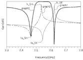
도 2은 체적 음향 공진기를 포함하는 필터의 예시적인 회로도이고, 도 3는 도 2의 필터의 주파수 응답을 나타낸다. 2 is an exemplary circuit diagram of a filter including a volume acoustic resonator, and FIG. 3 shows the frequency response of the filter of FIG. 2.
도 2을 참조하면, 필터(10)는 제1 포트(P1)와 제2 포트(P2) 사이에 배치되는 시리즈 공진기(SE) 및 시리즈 공진기(SE)와 접지 사이에 배치되는 션트 공진기(SH)를 포함할 수 있다. 시리즈 공진기(SE) 및 션트 공진기(SH)는 도 1에 도시된 체적 음향 공진기에 대응될 수 있다. Referring to FIG. 2, the
도 2에서, 하나의 시리즈 공진기(SE) 및 하나의 션트 공진기(SH)가 도시되어 있으나, 실시예에 따라, 제1 포트(P1)와 제2 포트(P2) 사이에는 복수의 시리즈 공진기(SE)가 배치되고, 시리즈 공진기(SE) 각각와 접지 사이에 서로 다른 복수의 션트 공진기(SH)가 배치될 수 있다. 또한, 도 2에서 필터(10)가 시리즈 공진기(SE) 및 션트 공진기(SH)를 포함하여, 래더 타입으로 구성되는 것으로 도시되어 있으나, 실시예에 따라, 필터(10)는 래티스 타입으로 구성될 수 있다. In FIG. 2, one series resonator SE and one shunt resonator SH are illustrated, but according to an embodiment, a plurality of series resonators SE between the first port P1 and the second port P2 ) May be disposed, and a plurality of shunt resonators SH different from each of the series resonators SE and ground may be disposed. In addition, in FIG. 2, the
도 3를 참조하면, 제1 그래프(Graph 1)는 시리즈 공진기(SE)에 의한 주파수 응답(Z, Impedance)을 나타내고, 제2 그래프(Graph2)는 션트 공진기(SH)에 의한 주파수 응답(Z, Impedancece)을 나타내고, 제3 그래프(Graph 3)는 시리즈 공진기(SE) 및 션트 공진기(SH)를 포함하는 필터에 의한 주파수 응답(S-parameter)을 나타낸다. 3, the first graph (Graph 1) represents the frequency response (Z, Impedance) by the series resonator SE, the second graph (Graph2) is the frequency response (Z, by the shunt resonator SH) Impedancece), and the third graph (Graph 3) shows the frequency response (S-parameter) by the filter including the series resonator SE and the shunt resonator SH.
시리즈 공진기(SE)에 의한 주파수 응답은 공진 주파수(fr_SE) 및 반공진 주파수(fa_SE)를 가지고, 션트 공진기(SH)에 의한 주파수 응답은 공진 주파수(fr_SH) 및 반공진 주파수(fa_SH)를 가진다. The frequency response by the series resonator SE has a resonance frequency fr_SE and an anti-resonance frequency fa_SE, and the frequency response by a shunt resonator SH has a resonance frequency fr_SH and an anti-resonance frequency fa_SH.
필터(10)의 주파수 응답을 참조하면, 필터의 통과 대역(Pass band) 및 대역폭(Band width)은 시리즈 공진기(SE)의 반공진 주파수(fa_SE)와 션트 공진기(SH)의 공진 주파수(fr_SH)에 따라 결정된다.Referring to the frequency response of the
5세대(5G) 통신은 기존 LTE(Long Term Evolution) 통신 대비 더 많은 대용량의 데이터와 더 빠른 데이터 전송 속도로 더 많은 기기들을 효율적으로 연결할 것으로 기대되고 있다. 5th generation (5G) communication is expected to connect more devices efficiently with more large-capacity data and faster data transmission speed than existing LTE (Long Term Evolution) communication.
5세대 통신에서, 사용되는 주파수의 대역폭은 수백MHz 수준으로 매우 넓으나, 실제 채널당 할당되는 대역폭은 최대 100MHz 수준으로 상대적으로 좁은 실정이다. 따라서, 전체 대역폭이 넓어지고, 채널 간의 폭이 줄어듦에 따라, 고성능의 광대역 특성 및 우수한 감쇄 특성을 가지는 필터가 요구되고 있다. In the 5th generation communication, the bandwidth of the frequency used is very wide at the level of hundreds of MHz, but the bandwidth allocated per channel is relatively narrow at the maximum level of 100MHz. Accordingly, as the overall bandwidth is widened and the width between channels is reduced, a filter having high performance broadband characteristics and excellent attenuation characteristics is required.
구체적으로, LTE 통신 대역 중 가장 넓은 대역폭을 가지는 n41(2.496~2.690GHz) 대역의 경우 BW/fc(Bandwidth/Center frequency)는 0.0748에 해당하고, 5세대 통신의 n77(3.3~4.2GHz) 대역의 경우 BW/fc는 0.24에 해당하고, 5세대 통신의 n79(4.4~5.0GHz) 대역의 경우 BW/fc는 0.128에 해당한다. n41(2.496~2.690GHz) 대역, n77(3.3~4.2GHz) 대역, n79(4.4~5.0GHz) 대역을 비교하면, 5세대 통신의 n77(3.3~4.2GHz) 대역, n79(4.4~5.0GHz) 대역이, LTE 통신의 n41(2.496~2.690GHz) 대역 보다 높은 광대역 특성을 구비하여야 함을 알 수 있다. Specifically, in the case of the n41 (2.496-2.690 GHz) band having the widest bandwidth among LTE communication bands, the bandwidth/center frequency (BW/fc) corresponds to 0.0748, and the n77 (3.3-4.2 GHz) band of the 5th generation communication In the case of BW/fc corresponds to 0.24, and in the case of the n79 (4.4 to 5.0 GHz) band of 5th generation communication, BW/fc corresponds to 0.128. Comparing the n41 (2.496 to 2.690 GHz) band, n77 (3.3 to 4.2 GHz) band, and n79 (4.4 to 5.0 GHz) band, the n77 (3.3 to 4.2 GHz) band of the 5th generation communication, n79 (4.4 to 5.0 GHz) It can be seen that the band should have a higher broadband characteristic than the n41 (2.496-2.690 GHz) band of LTE communication.
광대역 특성이 요구될수록, 압전 결합 계수(piezoelectric coupling coefficient, kt2)가 커지는 것이 바람직하나, 압전 결합 계수의 상승을 위하여, 체적 음향 공진기의 압전층의 불순물 농도를 증가시키는 것은 한계가 있기 때문에, 광대역 필터를 제작시에, 성능 열화가 필연적으로 수반되게 된다. As the broadband characteristic is required, it is preferable that the piezoelectric coupling coefficient (kt 2 ) is increased, but for increasing the piezoelectric coupling coefficient, it is limited to increase the impurity concentration of the piezoelectric layer of the volume acoustic resonator, since it is limited. When manufacturing a filter, performance deterioration is inevitably involved.
본 발명의 일 실시예에 따른 프론트 엔드 모듈은 서로 다른 통과 대역을 가지는 복수의 필터를 조합하여, 5세대 이동통신의 전체 통과 대역을 지원하되, 서로 다른 통과 대역을 가지는 복수의 필터를 선택적으로 연결하여, 설계된 채널의 통과 대역을 각각 담당함으로써, 고성능의 광대역 특성 및 우수한 감쇄 특성을 구현할 수 있다. The front end module according to an embodiment of the present invention combines a plurality of filters having different pass bands to support the entire pass band of the 5th generation mobile communication, but selectively connects a plurality of filters having different pass bands. Thus, by performing each of the pass bands of the designed channel, it is possible to implement high performance broadband characteristics and excellent attenuation characteristics.
도 4은 본 발명의 일 실시예에 따른 프론트 엔드 모듈의 회로도이다. 4 is a circuit diagram of a front end module according to an embodiment of the present invention.
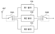
도 4을 참조하면, 본 발명의 일 실시예에 따른 프론트 엔드 모듈은 제1 필터(10A) 및 제2 필터(10B)를 포함하고, 제1 필터(10A) 및 제2 필터(10B)와 선택적으로 연결되는 제1 스위치(SWA) 및 제2 스위치(SWB)를 포함할 수 있다. 4, the front-end module according to an embodiment of the present invention includes a first filter (10A) and a second filter (10B), the first filter (10A) and the second filter (10B) and optional It may include a first switch (SWA) and the second switch (SWB) connected to.
제1 필터(10A), 및 제2 필터(10B)는 필터부를 구성할 수 있고, 제1 필터(10A), 및 제2 필터(10B) 각각은 대역 통과 필터를 포함할 수 있다. 일 예로, 제1 필터(10A), 및 제2 필터(10B)는 도 2의 필터(10)를 포함할 수 있고, 따라서, 제1 필터(10A), 및 제2 필터(10B) 각각은 적어도 하나의 체적 음향 공진기를 포함할 수 있다. 제1 필터(10A), 제2 필터(10B), 및 제3 필터(10C)는 하나의 칩(one-chip)에 의해 구현될 수 있다. The
제1 필터(10A) 및 제2 필터(10B)는 서로 다른 통과 대역(Pass band)를 가질 수 있다. 일 예로, 제1 필터(10A)의 통과 대역은 제2 필터(10B)의 통과 대역 보다 낮은 주파수 대역에 형성될 수 있다. The
제1 필터(10A)의 통과 대역과 제2 필터(10B)의 통과 대역은 일부 주파수 대역이 중첩될 수 있다. 따라서, 제1 필터(10A)의 상한 주파수는 제2 필터(10B)의 하한 주파수 보다 높은 주파수 대역에 위치할 수 있다. Some frequency bands may overlap the pass band of the
제1 필터(10A)의 통과 대역 및 제2 필터(10B)의 통과 대역에 의해 중첩되는 대역폭은, 제1 필터(10A) 및 제2 필터(10B)가 지원하는 복수의 채널의 대역폭에 따라 결정될 수 있다. The bandwidth overlapped by the pass band of the
구체적으로, 제1 필터(10A) 및 제2 필터(10B)가 5세대 통신의 n77(3.3~4.2GHz) 대역을 담당하는 것으로 가정하면, n77(3.3~4.2GHz) 대역은 다양한 대역폭을 가지는 복수의 채널을 가질 수 있다. 예를 들어, n77(3.3~4.2GHz) 대역은 10MHz, 20MHz, 40MHz, 50MHz, 60MHz, 80MHz, 및 100MHz 등 다양한 대역폭을 가지는 채널을 가질 수 있다. Specifically, assuming that the
제1 필터(10A)의 통과 대역 및 제2 필터(10B)의 통과 대역에 의해 중첩되는 대역폭은, 다양한 대역폭을 가지는 복수의 채널 중 하나의 채널의 대역폭에 따라, 결정될 수 있다. 일 예로, 제1 필터(10A)의 통과 대역 및 제2 필터(10B)의 통과 대역에 의해 중첩되는 대역폭은, 제1 필터(10A) 및 제2 필터(10B)가 지원하는 복수의 채널 중 최대 대역폭을 가지는 채널에 따라 결정될 수 있다. 구체적으로, 제1 필터(10A)의 통과 대역과 제2 필터(10B)의 통과 대역에 의해 중첩되는 대역폭 최대 대역폭을 가지는 채널의 대역폭과 동일하거나 클 수 있다. The bandwidth overlapped by the pass band of the
본 발명의 일 실시예에 따르면, 최대 대역폭을 가지는 채널의 대역폭에 따라, 제1 필터(10A)의 통과 대역 및 제2 필터(10B)의 통과 대역에 의해 중첩되는 대역폭을 결정하여, 제1 필터(10A) 및 제2 필터(10B)가 선택적으로 동작하는 경우에도, 채널들을 안정적으로 지원할 수 있다. According to an embodiment of the present invention, according to a bandwidth of a channel having a maximum bandwidth, a first filter is determined by determining a bandwidth overlapped by a pass band of the
한편, 제1 필터(10A) 및 제2 필터(10B)의 통과 대역(Pass band)의 대역폭(Band width)은 동일하게 설계될 수 있다. 다만, 실시예에 따라, 제1 필터(10A) 및 제2 필터(10B)의 통과 대역(Pass band)의 대역폭(Band width)은 서로 다르게 설계될 수 있다. Meanwhile, the bandwidths of the pass bands of the
제1 스위치(SWA) 및 제2 스위치(SWB)는 스위치부를 구성할 수 있다. 제1 스위치(SWA)는 일 단이 안테나와 연결되고, 타단이 제1 필터(10A) 및 제2 필터(10B)와 연결될 수 있다. 제2 스위치(SWB)는 일단이 저잡음 증폭기(LNA) 및 RF IC 등과 같은 무선 주파수 신호 처리 소자와 연결될 수 있고, 타단이 제1 필터(10A) 및 제2 필터(10B)와 연결될 수 있다.The first switch SWA and the second switch SWB may constitute a switch unit. One end of the first switch SWA may be connected to the antenna, and the other end may be connected to the
제1 스위치(SWA) 및 제2 스위치(SWB)는 제1 필터(10A) 및 제2 필터(10B)와 선택적으로 연결되어, 무선 주파수 신호의 경로를 형성할 수 있다. 제1 스위치(SWA) 및 제2 스위치(SWB)는 제1 필터(10A) 및 제2 필터(10B) 중 하나의 필터와 연결될 수 있다. 일 예로, 제1 필터(10A)의 동작 타이밍에서, 제1 스위치(SWA) 및 제2 스위치(SWB)는 제1 필터(10A)와 연결될 수 있고, 제2 필터(10B)의 동작 타이밍에서, 제1 스위치(SWA) 및 제2 스위치(SWB)는 제2 필터(10B)와 연결될 수 있다. The first switch SWA and the second switch SWB may be selectively connected to the
도 5은 본 발명의 일 실시예에 따른 프론트 엔드 모듈의 회로도이고, 도 6는 도 5의 프론트 엔드 모듈의 복수의 필터가 담당하는 통과 대역을 나타낸다. 도 5의 프론트 엔드 모듈은 도 4의 프론트 엔드 모듈과 유사하므로, 중복되는 설명은 생략하고, 차이점을 중심으로 설명하도록 한다. FIG. 5 is a circuit diagram of a front end module according to an embodiment of the present invention, and FIG. 6 shows a pass band covered by a plurality of filters of the front end module of FIG. 5. Since the front-end module of FIG. 5 is similar to the front-end module of FIG. 4, redundant description will be omitted and the difference will be mainly described.
도 5을 참조하면, 본 발명의 일 실시예에 따른 프론트 엔드 모듈은 제1 필터(10A), 제2 필터(10B), 및 제3 필터(10C)를 포함하고, 제1 필터(10A), 제2 필터(10B), 및 제3 필터(10C)와 선택적으로 연결되는 제1 스위치(SWA) 및 제2 스위치(SWB)를 포함할 수 있다. 5, the front end module according to an embodiment of the present invention includes a first filter (10A), a second filter (10B), and a third filter (10C), the first filter (10A), The
제1 필터(10A), 제2 필터(10B), 및 제3 필터(10C)는 필터부를 구성할 수 있고, 제1 필터(10A), 제2 필터(10B), 및 제3 필터(10C) 각각은 대역 통과 필터를 포함할 수 있다. 일 예로, 제1 필터(10A), 제2 필터(10B), 및 제3 필터(10C)는 도 2의 필터(10)를 포함할 수 있고, 따라서, 제1 필터(10A), 제2 필터(10B), 및 제3 필터(10C) 각각은 적어도 하나의 체적 음향 공진기를 포함할 수 있다. 제1 필터(10A), 제2 필터(10B), 및 제3 필터(10C)는 하나의 칩(one-chip)에 의해 구현될 수 있다. The
제1 필터(10A), 제2 필터(10B), 및 제3 필터(10C)는 서로 다른 통과 대역(Pass band)를 가질 수 있다. 도 6를 참조하면, 제1 필터(10A)에 의한 주파수 응답(f1), 제2 필터(10B)에 의한 주파수 응답(f2), 및 제3 필터(10C)에 의한 주파수 응답(f3)을 참조하면, 제1 필터(10A)의 통과 대역은 제2 필터(10B)의 통과 대역 보다 낮은 주파수 대역에 형성될 수 있고, 제2 필터(10B)의 통과 대역은 제3 필터(10C)의 통과 대역 보다 낮은 주파수 대역에 형성될 수 있다. 도 6의 제1 필터(10A)에 의한 주파수 응답(f1), 제2 필터(10B)에 의한 주파수 응답(f2), 및 제3 필터(10C)한 주파수 응답(f3)에 의해, 5세대 이동통신의 전체 통과 대역의 주파수 응답(f4)이 커버될 수 있다.The
제1 필터(10A)의 통과 대역과 제2 필터(10B)의 통과 대역은 일부 주파수 대역이 중첩될 수 있고, 제2 필터(10B)의 통과 대역과 제3 필터(10C)의 통과 대역은 일부 주파수 대역이 중첩될 수 있다. 따라서, 제1 필터(10A)의 상한 주파수는 제2 필터(10B)의 하한 주파수 보다 높은 주파수 대역에 위치할 수 있고, 제2 필터(10B)의 상한 주파수는 제3 필터(10C)의 하한 주파수 보다 높은 주파수 대역에 위치할 수 있다. The pass band of the
제1 필터(10A)의 통과 대역과 제2 필터(10B)의 통과 대역에 의해 중첩되는 대역폭 및 제2 필터(10B)의 통과 대역과 제3 필터(10C)의 통과 대역에 의해 중첩되는 대역폭은, 제1 필터(10A), 제2 필터(10B), 및 제3 필터(10C)가 지원하는 복수의 채널의 대역폭에 따라 결정될 수 있다. The bandwidth overlapped by the pass band of the
구체적으로, 제1 필터(10A), 제2 필터(10B), 및 제3 필터(10C)가 5세대 통신의 n77(3.3~4.2GHz) 대역을 담당하는 것으로 가정하면, n77(3.3~4.2GHz) 대역은 다양한 대역폭을 가지는 복수의 채널을 가질 수 있다. 예를 들어, n77(3.3~4.2GHz) 대역은 10MHz, 20MHz, 40MHz, 50MHz, 60MHz, 80MHz, 및 100MHz 등 다양한 대역폭을 가지는 채널을 가질 수 있다. Specifically, assuming that the
제1 필터(10A)의 통과 대역과 제2 필터(10B)의 통과 대역에 의해 중첩되는 대역폭, 및 제2 필터(10B)의 통과 대역과 제3 필터(10C)의 통과 대역에 의해 중첩되는 대역폭은, 다양한 대역폭을 가지는 복수의 채널 중 하나의 채널의 대역폭에 따라, 결정될 수 있다. 일 예로, 제1 필터(10A)의 통과 대역과 제2 필터(10B)의 통과 대역에 의해 중첩되는 대역폭 및 제2 필터(10B)의 통과 대역과 제3 필터(10C)의 통과 대역에 의해 중첩되는 대역폭은, 제1 필터(10A), 제2 필터(10B), 및 제3 필터(10C)가 지원하는 복수의 채널 중 최대 대역폭을 가지는 채널에 따라 결정될 수 있다. 구체적으로, 제1 필터(10A)의 통과 대역과 제2 필터(10B)의 통과 대역에 의해 중첩되는 대역폭 및 제2 필터(10B)의 통과 대역과 제3 필터(10C)의 통과 대역에 의해 중첩되는 대역폭은 최대 대역폭을 가지는 채널의 대역폭과 동일하거나 클 수 있다. Bandwidth overlapped by the passband of the
본 발명의 일 실시예에 따르면, 최대 대역폭을 가지는 채널의 대역폭에 따라, 제1 필터(10A)의 통과 대역과 제2 필터(10B)의 통과 대역에 의해 중첩되는 대역폭 및 제2 필터(10B)의 통과 대역과 제3 필터(10C)의 통과 대역에 의해 중첩되는 대역폭을 결정하여, 제1 필터(10A), 제2 필터(10B), 및 제3 필터(10C)가 선택적으로 동작하는 경우에도, 채널들을 안정적으로 지원할 수 있다. According to an embodiment of the present invention, according to the bandwidth of the channel having the maximum bandwidth, the bandwidth and the
한편, 제1 필터(10A), 제2 필터(10B), 및 제3 필터(10C)의 통과 대역(Pass band)의 대역폭(Band width)은 동일하게 설계될 수 있다. 다만, 실시예에 따라, 제1 필터(10A), 제2 필터(10B), 및 제3 필터(10C)의 통과 대역(Pass band)의 대역폭(Band width)은 서로 다르게 설계될 수 있다. Meanwhile, the bandwidths of the pass bands of the
제1 스위치(SWA) 및 제2 스위치(SWB)는 스위치부를 구성할 수 있다. 제1 스위치(SWA)는 일 단이 안테나와 연결되고, 타단이 제1 필터(10A), 제2 필터(10B) 및 제3 필터(10C)와 연결될 수 있다. 제2 스위치(SWB)는 일단이 저잡음 증폭기(LNA) 및 RF IC 등과 같은 무선 주파수 신호 처리 소자와 연결될 수 있고, 타단이 제1 필터(10A), 제2 필터(10B) 및 제3 필터(10C)와 연결될 수 있다.The first switch SWA and the second switch SWB may constitute a switch unit. One end of the first switch SWA may be connected to the antenna, and the other end may be connected to the
제1 스위치(SWA) 및 제2 스위치(SWB)는 제1 필터(10A), 제2 필터(10B) 및 제3 필터(10C)와 선택적으로 연결되어, 무선 주파수 신호의 경로를 형성할 수 있다. 제1 스위치(SWA) 및 제2 스위치(SWB)는 제1 필터(10A), 제2 필터(10B) 및 제3 필터(10C) 중 하나의 필터와 연결될 수 있다. 일 예로, 제1 필터(10A)의 동작 타이밍에서, 제1 스위치(SWA) 및 제2 스위치(SWB)는 제1 필터(10A)와 연결될 수 있고, 제2 필터(10B)의 동작 타이밍에서, 제1 스위치(SWA) 및 제2 스위치(SWB)는 제2 필터(10B)와 연결될 수 있고, 제3 필터(10C)의 동작 타이밍에서, 제1 스위치(SWA) 및 제2 스위치(SWB)는 제3 필터(10C)와 연결될 수 있다. The first switch SWA and the second switch SWB are selectively connected to the
이상에서 본 발명이 구체적인 구성요소 등과 같은 특정 사항들과 한정된 실시예 및 도면에 의해 설명되었으나, 이는 본 발명의 보다 전반적인 이해를 돕기 위해서 제공된 것일 뿐, 본 발명이 상기 실시예들에 한정되는 것은 아니며, 본 발명이 속하는 기술분야에서 통상적인 지식을 가진 자라면 이러한 기재로부터 다양한 수정 및 변형을 꾀할 수 있다.In the above, the present invention has been described by specific matters such as specific components, etc. and limited embodiments and drawings, which are provided to help the overall understanding of the present invention, but the present invention is not limited to the above embodiments , Those skilled in the art to which the present invention pertains can make various modifications and variations from these descriptions.
따라서, 본 발명의 사상은 상기 설명된 실시예에 국한되어 정해져서는 아니 되며, 후술하는 특허청구범위뿐만 아니라 이 특허청구범위와 균등하게 또는 등가적으로 변형된 모든 것들은 본 발명의 사상의 범주에 속한다고 할 것이다.Therefore, the spirit of the present invention is not limited to the above-described embodiment, and should not be determined, and all claims that are equally or equivalently modified with the claims as described below belong to the scope of the spirit of the present invention. Would say
10: 필터
10A: 제1 필터
10B: 제2 필터
10C: 제3 필터
SWA: 제1 스위치
SWB: 제2 스위치
SE: 시리즈 공진기
SH: 션트 공진기10: filter
10A: first filter
10B: second filter
10C: third filter
SWA: 1st switch
SWB: second switch
SE: Series resonators
SH: Shunt resonator
Claims (16)
상기 복수의 필터 중 하나와 선택적으로 연결되어, 무선 주파수 신호의 경로를 형성하는 스위치부; 를 포함하고,
상기 서로 다른 통과 대역 중 인접하는 두 개의 통과 대역 중 하나의 통과 대역의 일부 주파수 대역과 다른 하나의 통과 대역의 일부 주파수 대역은 서로 중첩되는 프론트 엔드 모듈.
A filter unit including at least one volume acoustic resonator including a first electrode, a piezoelectric layer, and a second electrode sequentially stacked, and including a plurality of filters in charge of different pass bands; And
A switch unit selectively connected to one of the plurality of filters to form a path of a radio frequency signal; Including,
A front end module in which some frequency bands of one of the two adjacent pass bands and the other frequency bands of the other one of the different pass bands overlap each other.
상기 두 개의 통과 대역에 의해 중첩되는 대역폭은, 상기 복수의 필터가 지원하는 복수의 채널 중 하나의 채널의 대역폭에 따라 결정되는 프론트 엔드 모듈.
According to claim 1,
The bandwidth overlapped by the two pass bands is determined by a bandwidth of one channel among a plurality of channels supported by the plurality of filters.
상기 두 개의 통과 대역에 의해 중첩되는 대역폭은, 상기 복수의 필터가 지원하는 복수의 채널 중 최대 대역폭을 가지는 채널의 대역폭에 따라 결정되는 프론트 엔드 모듈.
According to claim 2,
The bandwidth overlapped by the two pass bands is determined according to a bandwidth of a channel having a maximum bandwidth among a plurality of channels supported by the plurality of filters.
상기 복수의 필터 각각은 대역 통과 필터를 포함하는 프론트 엔드 모듈.
According to claim 1,
Each of the plurality of filters includes a front-end module including a band pass filter.
상기 서로 다른 통과 대역의 대역폭은 동일한 프론트 엔드 모듈.
According to claim 1,
The bandwidth of the different pass bands is the same front end module.
상기 복수의 필터 각각의 일단과 안테나 사이에 배치되는 제1 스위치; 및
상기 복수의 필터 각각의 타단과 무선 주파수 신호 처리 소자 사이에 배치되는 제2 스위치; 를 포함하는 프론트 엔드 모듈.
The method of claim 1, wherein the switch unit,
A first switch disposed between one end of each of the plurality of filters and an antenna; And
A second switch disposed between the other end of each of the plurality of filters and a radio frequency signal processing element; Front end module comprising a.
상기 적어도 하나의 체적 음향 공진기는 래더 타입 및 래티스 타입 중 적어도 하나의 형태로 연결되는 프론트 엔드 모듈.
According to claim 1,
The at least one volume acoustic resonator is a front end module connected to at least one of a ladder type and a lattice type.
상기 복수의 필터 중 하나와 선택적으로 연결되어, 무선 주파수 신호의 경로를 형성하는 스위치부; 를 포함하고,
상기 복수의 통과 대역 중 인접하는 제1 통과 대역 및 상기 제1 통과 대역 보다 주파수 대역이 높은 제2 통과 대역에 있어서, 상기 제1 통과 대역의 상한 주파수는 상기 제2 통과 대역의 하한 주파수 보다 주파수가 높은 프론트 엔드 모듈.
A filter unit including at least one volume acoustic resonator each including a first electrode, a piezoelectric layer, and a second electrode sequentially stacked, and including a plurality of filters for different pass bands among the plurality of pass bands; And
A switch unit selectively connected to one of the plurality of filters to form a path of a radio frequency signal; Including,
In a first pass band adjacent among the plurality of pass bands and a second pass band having a higher frequency band than the first pass band, the upper limit frequency of the first pass band has a frequency higher than the lower limit frequency of the second pass band. High front end module.
상기 제1 통과 대역 및 제2 통과 대역에 의해 중첩되는 대역폭은, 상기 복수의 필터가 지원하는 복수의 채널 중 하나의 채널의 대역폭에 따라 결정되는 프론트 엔드 모듈.
The method of claim 8,
The bandwidth overlapped by the first passband and the second passband is determined by a bandwidth of one channel among a plurality of channels supported by the plurality of filters.
상기 제1 통과 대역 및 제2 통과 대역에 의해 중첩되는 대역폭은, 상기 복수의 필터가 지원하는 복수의 채널 중 최대 대역폭을 가지는 채널의 대역폭에 따라 결정되는 프론트 엔드 모듈.
The method of claim 9,
The bandwidth overlapped by the first pass band and the second pass band is determined according to a bandwidth of a channel having a maximum bandwidth among a plurality of channels supported by the plurality of filters.
상기 복수의 필터 각각은 대역 통과 필터를 포함하는 프론트 엔드 모듈.
The method of claim 8,
Each of the plurality of filters includes a front-end module including a band pass filter.
상기 제1 통과 대역을 담당하는 제1 필터 및 상기 제2 통과 대역을 담당하는 제2 필터를 포함하는 프론트 엔드 모듈.
The method of claim 8, wherein the filter unit,
A front end module including a first filter in charge of the first pass band and a second filter in charge of the second pass band.
상기 제2 통과 대역 보다 주파수 대역이 높은 제3 통과 대역을 담당하는 제3 필터를 더 포함하는 프론트 엔드 모듈.
The method of claim 12, wherein the filter unit,
A front end module further comprising a third filter in charge of a third pass band having a higher frequency band than the second pass band.
상기 제2 통과 대역의 상한 주파수는 상기 제3 통과 대역의 하한 주파수 보다 주파수가 높은 프론트 엔드 모듈.
The method of claim 13,
The front end module has a higher frequency than the lower limit frequency of the third pass band.
상기 복수의 필터는 하나의 칩으로 구현되는 프론트 엔드 모듈.
The method of claim 8,
The plurality of filters is a front end module implemented as a single chip.
상기 적어도 하나의 체적 음향 공진기는 래더 타입 및 래티스 타입 중 적어도 하나의 형태로 연결되는 프론트 엔드 모듈.
The method of claim 8,
The at least one volume acoustic resonator is a front end module connected to at least one of a ladder type and a lattice type.
Priority Applications (3)
| Application Number | Priority Date | Filing Date | Title |
|---|---|---|---|
| KR1020180167660A KR20200078084A (en) | 2018-12-21 | 2018-12-21 | Front end module |
| US16/416,505 US20200204157A1 (en) | 2018-12-21 | 2019-05-20 | Front end module |
| CN201910776907.XA CN111355471B (en) | 2018-12-21 | 2019-08-22 | Front end module |
Applications Claiming Priority (1)
| Application Number | Priority Date | Filing Date | Title |
|---|---|---|---|
| KR1020180167660A KR20200078084A (en) | 2018-12-21 | 2018-12-21 | Front end module |
Publications (1)
| Publication Number | Publication Date |
|---|---|
| KR20200078084A true KR20200078084A (en) | 2020-07-01 |
Family
ID=71097919
Family Applications (1)
| Application Number | Title | Priority Date | Filing Date |
|---|---|---|---|
| KR1020180167660A KR20200078084A (en) | 2018-12-21 | 2018-12-21 | Front end module |
Country Status (3)
| Country | Link |
|---|---|
| US (1) | US20200204157A1 (en) |
| KR (1) | KR20200078084A (en) |
| CN (1) | CN111355471B (en) |
Families Citing this family (1)
| Publication number | Priority date | Publication date | Assignee | Title |
|---|---|---|---|---|
| WO2022018997A1 (en) * | 2020-07-21 | 2022-01-27 | 株式会社村田製作所 | High frequency circuit |
Citations (1)
| Publication number | Priority date | Publication date | Assignee | Title |
|---|---|---|---|---|
| KR20080081398A (en) | 2007-03-05 | 2008-09-10 | 주식회사 하이닉스반도체 | Method of forming field oxide layer in semiconductor device |
Family Cites Families (8)
| Publication number | Priority date | Publication date | Assignee | Title |
|---|---|---|---|---|
| FI106894B (en) * | 1998-06-02 | 2001-04-30 | Nokia Mobile Phones Ltd | resonator structures |
| GB2346049A (en) * | 1999-01-19 | 2000-07-26 | Roke Manor Research | Duplex filtering |
| KR100666693B1 (en) * | 2004-11-23 | 2007-01-11 | 삼성전자주식회사 | Monolithic duplexer |
| US9038005B2 (en) * | 2013-03-15 | 2015-05-19 | Resonant Inc. | Network synthesis design of microwave acoustic wave filters |
| JP6133504B2 (en) * | 2013-06-26 | 2017-05-24 | インテル アイピー コーポレーション | Bulk acoustic wave resonator tuner circuit |
| US10439589B2 (en) * | 2016-06-24 | 2019-10-08 | Samsung Electro-Mechanics Co., Ltd. | Bulk acoustic wave resonator and filter including the same |
| US10256792B2 (en) * | 2017-02-03 | 2019-04-09 | Samsung Electro-Mechanics Co., Ltd. | Filter module and front-end module including the same |
| WO2019021983A1 (en) * | 2017-07-25 | 2019-01-31 | 株式会社村田製作所 | High frequency filter, multiplexer, high frequency front-end circuit, and communication device |
-
2018
- 2018-12-21 KR KR1020180167660A patent/KR20200078084A/en not_active Application Discontinuation
-
2019
- 2019-05-20 US US16/416,505 patent/US20200204157A1/en not_active Abandoned
- 2019-08-22 CN CN201910776907.XA patent/CN111355471B/en active Active
Patent Citations (1)
| Publication number | Priority date | Publication date | Assignee | Title |
|---|---|---|---|---|
| KR20080081398A (en) | 2007-03-05 | 2008-09-10 | 주식회사 하이닉스반도체 | Method of forming field oxide layer in semiconductor device |
Also Published As
| Publication number | Publication date |
|---|---|
| CN111355471A (en) | 2020-06-30 |
| US20200204157A1 (en) | 2020-06-25 |
| CN111355471B (en) | 2023-09-12 |
Similar Documents
| Publication | Publication Date | Title |
|---|---|---|
| CN107786182B (en) | Bulk acoustic wave resonator and filter including the same | |
| JP4654220B2 (en) | Filter structure including a piezoelectric resonator | |
| KR100506729B1 (en) | Film bulk acoustic resonator and method for fabrication thereof | |
| JP6556099B2 (en) | Piezoelectric thin film resonator, filter and multiplexer | |
| JP6510987B2 (en) | Piezoelectric thin film resonator, filter and duplexer | |
| KR20190084008A (en) | Acoustic resonator and method of manufacturing thereof | |
| US10965271B2 (en) | Acoustic resonator and method for fabricating the same | |
| CN107317561B (en) | Bulk acoustic wave resonator and method for manufacturing the same | |
| JP2019016835A (en) | Piezoelectric thin film resonator, filter and multiplexer | |
| JP2018182463A (en) | Piezoelectric thin film resonator, filter and multiplexer | |
| KR102052795B1 (en) | Acoustic resonator | |
| US11418168B2 (en) | Acoustic resonator and method for manufacturing the same | |
| US20210297063A1 (en) | Filter with volume acoustic resonators | |
| US20150130561A1 (en) | Piezoelectric thin film resonator, filter and duplexer | |
| US10523177B2 (en) | Piezoelectric thin film resonator and fabrication method of the same, filter, and multiplexer | |
| KR102449355B1 (en) | Acoustic resonator and method for fabricating the same | |
| KR102145309B1 (en) | Acoustic resonator | |
| KR20180023787A (en) | Bulk-acoustic wave resonator and filter having the same | |
| CN111355471B (en) | Front end module | |
| KR102449367B1 (en) | Acoustic resonator and method for fabricating the same | |
| KR102100125B1 (en) | Filter | |
| US20200350892A1 (en) | Front end module | |
| JP2019201305A (en) | Acoustic resonator | |
| KR102066959B1 (en) | Filter | |
| KR20220168424A (en) | Bulk-acoustic wave resonator |
Legal Events
| Date | Code | Title | Description |
|---|---|---|---|
| E601 | Decision to refuse application |