KR20200057372A - DOPED TIN OXIDE THIN FILE TRANSISTOR and manufacturing method thereof - Google Patents
DOPED TIN OXIDE THIN FILE TRANSISTOR and manufacturing method thereof Download PDFInfo
- Publication number
- KR20200057372A KR20200057372A KR1020180141672A KR20180141672A KR20200057372A KR 20200057372 A KR20200057372 A KR 20200057372A KR 1020180141672 A KR1020180141672 A KR 1020180141672A KR 20180141672 A KR20180141672 A KR 20180141672A KR 20200057372 A KR20200057372 A KR 20200057372A
- Authority
- KR
- South Korea
- Prior art keywords
- thin film
- film transistor
- channel layer
- tin oxide
- tin
- Prior art date
Links
- 229910001887 tin oxide Inorganic materials 0.000 title claims abstract description 69
- 238000004519 manufacturing process Methods 0.000 title claims abstract description 24
- DDSPUNTXKUFWTM-UHFFFAOYSA-N oxygen(2-);tin(4+) Chemical compound [O-2].[O-2].[Sn+4] DDSPUNTXKUFWTM-UHFFFAOYSA-N 0.000 title 1
- XOLBLPGZBRYERU-UHFFFAOYSA-N tin dioxide Chemical compound O=[Sn]=O XOLBLPGZBRYERU-UHFFFAOYSA-N 0.000 claims abstract description 130
- 239000010409 thin film Substances 0.000 claims abstract description 97
- 229910052782 aluminium Inorganic materials 0.000 claims abstract description 69
- XAGFODPZIPBFFR-UHFFFAOYSA-N aluminium Chemical compound [Al] XAGFODPZIPBFFR-UHFFFAOYSA-N 0.000 claims abstract description 65
- 238000000034 method Methods 0.000 claims description 59
- 229910006404 SnO 2 Inorganic materials 0.000 claims description 38
- 238000000137 annealing Methods 0.000 claims description 35
- 239000000758 substrate Substances 0.000 claims description 32
- XKRFYHLGVUSROY-UHFFFAOYSA-N Argon Chemical compound [Ar] XKRFYHLGVUSROY-UHFFFAOYSA-N 0.000 claims description 26
- ATJFFYVFTNAWJD-UHFFFAOYSA-N Tin Chemical compound [Sn] ATJFFYVFTNAWJD-UHFFFAOYSA-N 0.000 claims description 21
- 238000000231 atomic layer deposition Methods 0.000 claims description 17
- 229910018072 Al 2 O 3 Inorganic materials 0.000 claims description 15
- TWNQGVIAIRXVLR-UHFFFAOYSA-N oxo(oxoalumanyloxy)alumane Chemical compound O=[Al]O[Al]=O TWNQGVIAIRXVLR-UHFFFAOYSA-N 0.000 claims description 14
- 229910052786 argon Inorganic materials 0.000 claims description 13
- QVGXLLKOCUKJST-UHFFFAOYSA-N atomic oxygen Chemical compound [O] QVGXLLKOCUKJST-UHFFFAOYSA-N 0.000 claims description 13
- 239000001301 oxygen Substances 0.000 claims description 13
- 229910052760 oxygen Inorganic materials 0.000 claims description 13
- 238000010926 purge Methods 0.000 claims description 12
- 230000000694 effects Effects 0.000 claims description 8
- 239000000126 substance Substances 0.000 claims description 8
- 230000005669 field effect Effects 0.000 claims description 7
- 239000002243 precursor Substances 0.000 claims description 5
- CBENFWSGALASAD-UHFFFAOYSA-N Ozone Chemical group [O-][O+]=O CBENFWSGALASAD-UHFFFAOYSA-N 0.000 claims description 3
- 238000007254 oxidation reaction Methods 0.000 claims description 2
- 239000013626 chemical specie Substances 0.000 claims 1
- 239000010410 layer Substances 0.000 description 131
- 230000000052 comparative effect Effects 0.000 description 36
- 238000000151 deposition Methods 0.000 description 23
- 230000008021 deposition Effects 0.000 description 19
- 239000004065 semiconductor Substances 0.000 description 11
- 238000002425 crystallisation Methods 0.000 description 8
- 230000008025 crystallization Effects 0.000 description 8
- 239000010408 film Substances 0.000 description 8
- 238000005229 chemical vapour deposition Methods 0.000 description 7
- 238000004544 sputter deposition Methods 0.000 description 7
- 239000013078 crystal Substances 0.000 description 5
- 238000000059 patterning Methods 0.000 description 5
- GWEVSGVZZGPLCZ-UHFFFAOYSA-N Titan oxide Chemical compound O=[Ti]=O GWEVSGVZZGPLCZ-UHFFFAOYSA-N 0.000 description 4
- 230000003111 delayed effect Effects 0.000 description 4
- 238000010586 diagram Methods 0.000 description 4
- 229910052751 metal Inorganic materials 0.000 description 4
- 239000002184 metal Substances 0.000 description 4
- KFZMGEQAYNKOFK-UHFFFAOYSA-N Isopropanol Chemical compound CC(C)O KFZMGEQAYNKOFK-UHFFFAOYSA-N 0.000 description 3
- 238000002441 X-ray diffraction Methods 0.000 description 3
- 229910021417 amorphous silicon Inorganic materials 0.000 description 3
- 239000011521 glass Substances 0.000 description 3
- 238000005259 measurement Methods 0.000 description 3
- 239000004033 plastic Substances 0.000 description 3
- CSCPPACGZOOCGX-UHFFFAOYSA-N Acetone Chemical compound CC(C)=O CSCPPACGZOOCGX-UHFFFAOYSA-N 0.000 description 2
- GYHNNYVSQQEPJS-UHFFFAOYSA-N Gallium Chemical compound [Ga] GYHNNYVSQQEPJS-UHFFFAOYSA-N 0.000 description 2
- XUIMIQQOPSSXEZ-UHFFFAOYSA-N Silicon Chemical compound [Si] XUIMIQQOPSSXEZ-UHFFFAOYSA-N 0.000 description 2
- 238000004458 analytical method Methods 0.000 description 2
- 230000015572 biosynthetic process Effects 0.000 description 2
- 229910052804 chromium Inorganic materials 0.000 description 2
- 229920001940 conductive polymer Polymers 0.000 description 2
- 239000004020 conductor Substances 0.000 description 2
- 230000006866 deterioration Effects 0.000 description 2
- 238000011156 evaluation Methods 0.000 description 2
- 229910052733 gallium Inorganic materials 0.000 description 2
- 229910052737 gold Inorganic materials 0.000 description 2
- 238000010438 heat treatment Methods 0.000 description 2
- 238000001755 magnetron sputter deposition Methods 0.000 description 2
- 239000000463 material Substances 0.000 description 2
- 238000012986 modification Methods 0.000 description 2
- 230000004048 modification Effects 0.000 description 2
- 229910021420 polycrystalline silicon Inorganic materials 0.000 description 2
- 229920000642 polymer Polymers 0.000 description 2
- 229920005591 polysilicon Polymers 0.000 description 2
- 229910052710 silicon Inorganic materials 0.000 description 2
- 239000010703 silicon Substances 0.000 description 2
- 229910052814 silicon oxide Inorganic materials 0.000 description 2
- 229910052709 silver Inorganic materials 0.000 description 2
- 229910017109 AlON Inorganic materials 0.000 description 1
- 229910017107 AlOx Inorganic materials 0.000 description 1
- -1 HfOx Inorganic materials 0.000 description 1
- 239000004642 Polyimide Substances 0.000 description 1
- 229910004205 SiNX Inorganic materials 0.000 description 1
- 229910004298 SiO 2 Inorganic materials 0.000 description 1
- VYPSYNLAJGMNEJ-UHFFFAOYSA-N Silicium dioxide Chemical compound O=[Si]=O VYPSYNLAJGMNEJ-UHFFFAOYSA-N 0.000 description 1
- 229910003070 TaOx Inorganic materials 0.000 description 1
- PNEYBMLMFCGWSK-UHFFFAOYSA-N aluminium oxide Inorganic materials [O-2].[O-2].[O-2].[Al+3].[Al+3] PNEYBMLMFCGWSK-UHFFFAOYSA-N 0.000 description 1
- 238000005266 casting Methods 0.000 description 1
- 238000006243 chemical reaction Methods 0.000 description 1
- 239000011248 coating agent Substances 0.000 description 1
- 238000000576 coating method Methods 0.000 description 1
- 230000000593 degrading effect Effects 0.000 description 1
- 239000008367 deionised water Substances 0.000 description 1
- 229910021641 deionized water Inorganic materials 0.000 description 1
- 238000009792 diffusion process Methods 0.000 description 1
- 238000003618 dip coating Methods 0.000 description 1
- 239000012776 electronic material Substances 0.000 description 1
- 230000001747 exhibiting effect Effects 0.000 description 1
- 239000011888 foil Substances 0.000 description 1
- 239000011810 insulating material Substances 0.000 description 1
- 229960004592 isopropanol Drugs 0.000 description 1
- WHXTVQNIFGXMSB-UHFFFAOYSA-N n-methyl-n-[tris(dimethylamino)stannyl]methanamine Chemical compound CN(C)[Sn](N(C)C)(N(C)C)N(C)C WHXTVQNIFGXMSB-UHFFFAOYSA-N 0.000 description 1
- 229910052759 nickel Inorganic materials 0.000 description 1
- 150000004767 nitrides Chemical class 0.000 description 1
- 230000003287 optical effect Effects 0.000 description 1
- 238000000206 photolithography Methods 0.000 description 1
- 238000000623 plasma-assisted chemical vapour deposition Methods 0.000 description 1
- 229920001721 polyimide Polymers 0.000 description 1
- 239000002861 polymer material Substances 0.000 description 1
- 239000011241 protective layer Substances 0.000 description 1
- 238000004528 spin coating Methods 0.000 description 1
- 238000005118 spray pyrolysis Methods 0.000 description 1
- OFIYHXOOOISSDN-UHFFFAOYSA-N tellanylidenegallium Chemical compound [Te]=[Ga] OFIYHXOOOISSDN-UHFFFAOYSA-N 0.000 description 1
- 229910052719 titanium Inorganic materials 0.000 description 1
- XLYOFNOQVPJJNP-UHFFFAOYSA-N water Chemical compound O XLYOFNOQVPJJNP-UHFFFAOYSA-N 0.000 description 1
- 238000001039 wet etching Methods 0.000 description 1
Images


Classifications
-
- H—ELECTRICITY
- H01—ELECTRIC ELEMENTS
- H01L—SEMICONDUCTOR DEVICES NOT COVERED BY CLASS H10
- H01L29/00—Semiconductor devices adapted for rectifying, amplifying, oscillating or switching, or capacitors or resistors with at least one potential-jump barrier or surface barrier, e.g. PN junction depletion layer or carrier concentration layer; Details of semiconductor bodies or of electrodes thereof ; Multistep manufacturing processes therefor
- H01L29/66—Types of semiconductor device ; Multistep manufacturing processes therefor
- H01L29/68—Types of semiconductor device ; Multistep manufacturing processes therefor controllable by only the electric current supplied, or only the electric potential applied, to an electrode which does not carry the current to be rectified, amplified or switched
- H01L29/76—Unipolar devices, e.g. field effect transistors
- H01L29/772—Field effect transistors
- H01L29/78—Field effect transistors with field effect produced by an insulated gate
- H01L29/786—Thin film transistors, i.e. transistors with a channel being at least partly a thin film
- H01L29/7869—Thin film transistors, i.e. transistors with a channel being at least partly a thin film having a semiconductor body comprising an oxide semiconductor material, e.g. zinc oxide, copper aluminium oxide, cadmium stannate
-
- H—ELECTRICITY
- H01—ELECTRIC ELEMENTS
- H01L—SEMICONDUCTOR DEVICES NOT COVERED BY CLASS H10
- H01L21/00—Processes or apparatus adapted for the manufacture or treatment of semiconductor or solid state devices or of parts thereof
- H01L21/02—Manufacture or treatment of semiconductor devices or of parts thereof
- H01L21/02104—Forming layers
- H01L21/02107—Forming insulating materials on a substrate
- H01L21/02225—Forming insulating materials on a substrate characterised by the process for the formation of the insulating layer
- H01L21/0226—Forming insulating materials on a substrate characterised by the process for the formation of the insulating layer formation by a deposition process
- H01L21/02263—Forming insulating materials on a substrate characterised by the process for the formation of the insulating layer formation by a deposition process deposition from the gas or vapour phase
- H01L21/02271—Forming insulating materials on a substrate characterised by the process for the formation of the insulating layer formation by a deposition process deposition from the gas or vapour phase deposition by decomposition or reaction of gaseous or vapour phase compounds, i.e. chemical vapour deposition
- H01L21/0228—Forming insulating materials on a substrate characterised by the process for the formation of the insulating layer formation by a deposition process deposition from the gas or vapour phase deposition by decomposition or reaction of gaseous or vapour phase compounds, i.e. chemical vapour deposition deposition by cyclic CVD, e.g. ALD, ALE, pulsed CVD
-
- H—ELECTRICITY
- H01—ELECTRIC ELEMENTS
- H01L—SEMICONDUCTOR DEVICES NOT COVERED BY CLASS H10
- H01L21/00—Processes or apparatus adapted for the manufacture or treatment of semiconductor or solid state devices or of parts thereof
- H01L21/02—Manufacture or treatment of semiconductor devices or of parts thereof
- H01L21/04—Manufacture or treatment of semiconductor devices or of parts thereof the devices having at least one potential-jump barrier or surface barrier, e.g. PN junction, depletion layer or carrier concentration layer
- H01L21/18—Manufacture or treatment of semiconductor devices or of parts thereof the devices having at least one potential-jump barrier or surface barrier, e.g. PN junction, depletion layer or carrier concentration layer the devices having semiconductor bodies comprising elements of Group IV of the Periodic System or AIIIBV compounds with or without impurities, e.g. doping materials
- H01L21/30—Treatment of semiconductor bodies using processes or apparatus not provided for in groups H01L21/20 - H01L21/26
- H01L21/324—Thermal treatment for modifying the properties of semiconductor bodies, e.g. annealing, sintering
-
- H—ELECTRICITY
- H01—ELECTRIC ELEMENTS
- H01L—SEMICONDUCTOR DEVICES NOT COVERED BY CLASS H10
- H01L29/00—Semiconductor devices adapted for rectifying, amplifying, oscillating or switching, or capacitors or resistors with at least one potential-jump barrier or surface barrier, e.g. PN junction depletion layer or carrier concentration layer; Details of semiconductor bodies or of electrodes thereof ; Multistep manufacturing processes therefor
- H01L29/66—Types of semiconductor device ; Multistep manufacturing processes therefor
- H01L29/66007—Multistep manufacturing processes
- H01L29/66075—Multistep manufacturing processes of devices having semiconductor bodies comprising group 14 or group 13/15 materials
- H01L29/66227—Multistep manufacturing processes of devices having semiconductor bodies comprising group 14 or group 13/15 materials the devices being controllable only by the electric current supplied or the electric potential applied, to an electrode which does not carry the current to be rectified, amplified or switched, e.g. three-terminal devices
- H01L29/66409—Unipolar field-effect transistors
- H01L29/66477—Unipolar field-effect transistors with an insulated gate, i.e. MISFET
- H01L29/66742—Thin film unipolar transistors
-
- H—ELECTRICITY
- H01—ELECTRIC ELEMENTS
- H01L—SEMICONDUCTOR DEVICES NOT COVERED BY CLASS H10
- H01L29/00—Semiconductor devices adapted for rectifying, amplifying, oscillating or switching, or capacitors or resistors with at least one potential-jump barrier or surface barrier, e.g. PN junction depletion layer or carrier concentration layer; Details of semiconductor bodies or of electrodes thereof ; Multistep manufacturing processes therefor
- H01L29/66—Types of semiconductor device ; Multistep manufacturing processes therefor
- H01L29/68—Types of semiconductor device ; Multistep manufacturing processes therefor controllable by only the electric current supplied, or only the electric potential applied, to an electrode which does not carry the current to be rectified, amplified or switched
- H01L29/76—Unipolar devices, e.g. field effect transistors
- H01L29/772—Field effect transistors
- H01L29/78—Field effect transistors with field effect produced by an insulated gate
- H01L29/786—Thin film transistors, i.e. transistors with a channel being at least partly a thin film
- H01L29/78606—Thin film transistors, i.e. transistors with a channel being at least partly a thin film with supplementary region or layer in the thin film or in the insulated bulk substrate supporting it for controlling or increasing the safety of the device
- H01L29/78618—Thin film transistors, i.e. transistors with a channel being at least partly a thin film with supplementary region or layer in the thin film or in the insulated bulk substrate supporting it for controlling or increasing the safety of the device characterised by the drain or the source properties, e.g. the doping structure, the composition, the sectional shape or the contact structure
-
- H—ELECTRICITY
- H01—ELECTRIC ELEMENTS
- H01L—SEMICONDUCTOR DEVICES NOT COVERED BY CLASS H10
- H01L29/00—Semiconductor devices adapted for rectifying, amplifying, oscillating or switching, or capacitors or resistors with at least one potential-jump barrier or surface barrier, e.g. PN junction depletion layer or carrier concentration layer; Details of semiconductor bodies or of electrodes thereof ; Multistep manufacturing processes therefor
- H01L29/66—Types of semiconductor device ; Multistep manufacturing processes therefor
- H01L29/68—Types of semiconductor device ; Multistep manufacturing processes therefor controllable by only the electric current supplied, or only the electric potential applied, to an electrode which does not carry the current to be rectified, amplified or switched
- H01L29/76—Unipolar devices, e.g. field effect transistors
- H01L29/772—Field effect transistors
- H01L29/78—Field effect transistors with field effect produced by an insulated gate
- H01L29/786—Thin film transistors, i.e. transistors with a channel being at least partly a thin film
- H01L29/78696—Thin film transistors, i.e. transistors with a channel being at least partly a thin film characterised by the structure of the channel, e.g. multichannel, transverse or longitudinal shape, length or width, doping structure, or the overlap or alignment between the channel and the gate, the source or the drain, or the contacting structure of the channel
Abstract
Description
본 발명은 도핑된 주석 산화물을 채널층으로 포함하여 스위칭 특성 및 전하 이동도가 향상된 박막 트랜지스터 및 그 제조 방법에 관한 것이다.The present invention relates to a thin film transistor including a doped tin oxide as a channel layer and improved switching characteristics and charge mobility, and a method for manufacturing the same.
박막 트랜지스터는 디스플레이 산업에서 분야에서 필수적으로 포함되는 소자이다. 특히 박막 트랜지스터는 LCD나 OLED와 같은 표시 장치에서 각각의 화소를 스위칭하는 핵심적인 기능을 수행한다. The thin film transistor is a device that is essentially included in the field in the display industry. In particular, a thin film transistor performs a key function of switching each pixel in a display device such as an LCD or OLED.
디스플레이가 대형화됨에 따라 대형 표시 장치의 구동을 위해서는 초고속 구동이 가능한 박막 트랜지스터가 요구된다.As the display becomes larger, a thin film transistor capable of driving at a very high speed is required for driving a large display device.
종래에는 액티브 층으로 비정질 실리콘이 주로 이용되었으나, 비정질 실리콘은 전자 이동도가 낮아 초고속 구동에 적용이 어렵다는 문제가 있었다. In the prior art, amorphous silicon was mainly used as the active layer, but the amorphous silicon had a problem that it was difficult to apply to ultra-high-speed driving due to low electron mobility.
비정질 실리콘을 대체하기 위해 높은 전자이동도를 가지는 저온폴리 실리콘과 산화물 반도체가 많은 관심을 받고 있다. In order to replace amorphous silicon, low-temperature polysilicon and oxide semiconductors having high electron mobility have attracted much attention.
이 중 저온폴리 실리콘은 공정이 복잡하고 반도체층의 균일도를 확보하는 것이 어렵다는 문제점이 있다. 이에 따라 실리콘 반도체 대비 낮은 누설 전류를 가지고 투명하면서 대면적 공정이 용이하다는 장점을 가지는 산화물 반도체가 최근 디스플레이 산업에서 주목을 받고 있다. Among them, low-temperature polysilicon has a problem that the process is complicated and it is difficult to secure the uniformity of the semiconductor layer. Accordingly, an oxide semiconductor having a low leakage current compared to a silicon semiconductor and having an advantage of being transparent and facilitating a large-area process has recently attracted attention in the display industry.
특히 산화물 반도체는 높은 이동도, 투명성, 플렉서블 기판에의 적용 가능성뿐만 아니라 낮은 증착 온도와 같은 다양한 장점을 가지고 있기 때문에 최근에는 산화물 반도체를 박막 트랜지스터에 활용하고자 하는 노력들이 증가하고 있다.In particular, since oxide semiconductors have various advantages such as high mobility, transparency, and applicability to flexible substrates, as well as low deposition temperature, efforts to utilize oxide semiconductors in thin film transistors have recently increased.
이러한 산화물 반도체 가운데 주석 산화물(tin oxide)은 오랫동안 연구되고 있는 산화물로 물리적, 화학적, 전기적 그리고 광학적 장점을 가진 전자 재료로써 주목을 받고 있다. 특히 이산화 주석(tin dioxide)는 다른 반도체 물질에 비해 높은 밴드갭으로 인해 투명성을 가지며 낮은 전기 비저항의 특성을 통해 투명전도막으로 큰 관심을 받고 있다.Among these oxide semiconductors, tin oxide is an oxide that has been studied for a long time and has attracted attention as an electronic material having physical, chemical, electrical and optical advantages. In particular, tin dioxide is highly transparent due to its high band gap compared to other semiconductor materials, and has received great attention as a transparent conductive film due to its low electrical resistivity.
그러나 주석 산화물은 주로 분무 열분해 공정을 통해 제조되는데, 상기 공정은 분문 장치 장치 자체가 대면적화에 적용이 어려워 생산성이 떨어질 뿐만 아니라 산화물 반도체에서는 필수적인 도핑이 쉽지 않아 적용이 매우 어렵다는 단점이 있다. However, tin oxide is mainly produced through a spray pyrolysis process, and the process has disadvantages in that it is difficult to apply because the dosing device itself is difficult to apply to a large area and is not easily doped in oxide semiconductors.
한편 현재의 디스플레이 산업에서 널리 사용되는 화학 기상 증착법은 균일하게 증착이 가능하며 후속 공정으로 미세 패터닝 공정을 진행할 수 있다는 장점이 있다. 그러나 화학 기상 증착법은 고품질의 주석 산화물을 얻기 위해 높은 공정온도가 필요하기 때문에 기판으로 플라스틱과 같은 유연 기판을 적용하지 못하며 더 나아가 도핑이 어렵다는 문제점이 있다.Meanwhile, the chemical vapor deposition method widely used in the current display industry has the advantage of being capable of uniformly depositing and performing a fine patterning process as a subsequent process. However, the chemical vapor deposition method does not apply a flexible substrate such as plastic as a substrate because it requires a high process temperature to obtain high quality tin oxide, and further, there is a problem that doping is difficult.
본 발명은 전술한 문제점을 해결하기 위한 것으로, 도핑된 주석 산화물 채널층을 포함하는 산화물 박막 트랜지스터를 제공하여 스위칭 소자에 대한 전기적 특성 개선시키는 것을 목적으로 한다.The present invention is to solve the above-described problems, and an object of the present invention is to provide an oxide thin film transistor including a doped tin oxide channel layer to improve electrical characteristics of a switching element.
또한 본 발명은 주석 산화물 채널층을 도핑함으로써 순수한 주석 산화물 대비 전하 농도는 감소하고 온/오프 전류 비(on/off current ratio) 비율은 향상된 산화물 박막 트랜지스터를 제공하는 것을 다른 목적으로 한다.Another object of the present invention is to provide an oxide thin film transistor having a reduced charge concentration compared to pure tin oxide and an improved on / off current ratio ratio by doping the tin oxide channel layer.
또한 본 발명은 대면적 공정에 적합하고 도핑 공정 및 열처리 공정 이후 전기적 특성이 향상된 산화물 박막 트랜지스터를 제공하는 것을 또 다른 목적으로 한다.In addition, another object of the present invention is to provide an oxide thin film transistor suitable for a large area process and having improved electrical properties after a doping process and a heat treatment process.
본 발명은 상기의 목적을 달성하기 위한 본 발명의 일 실시예에 따르면, 베이스 기판; 상기 베이스 기판 상에 위치하는 게이트 전극; 상기 게이트 전극 상에 위치하는 게이트 절연층; 상기 게이트 절연층 상에 위치하는 채널층; 상기 게이트 절연층 상에 위치하며 상기 채널층을 사이에 두고 상호 이격된 소스 전극과 드레인 전극;을 포함하고, 상기 채널층은 알루미늄이 도핑된 이산화 주석을 포함하며, 전하농도가 1016~1018/㎤인 것;을 특징으로 하는 박막 트랜지스터가 제공된다.The present invention according to an embodiment of the present invention for achieving the above object, the base substrate; A gate electrode positioned on the base substrate; A gate insulating layer on the gate electrode; A channel layer positioned on the gate insulating layer; Located on the gate insulating layer, the source electrode and the drain electrode spaced apart from each other with the channel layer interposed therebetween. The channel layer includes tin doped with aluminum, and has a charge concentration of 10 16 to 10 18. A thin film transistor characterized by being / cm 3 is provided.
바람직하게는, 상기 박막 트랜지스터는 전하 이동도(field effect mobility)가 0.1~4 ㎠/Vs인 것;을 특징으로 하는 박막 트랜지스터가 제공될 수 있다.Preferably, the thin film transistor has a charge effect (field effect mobility) of 0.1 ~ 4
바람직하게는, 상기 박막 트랜지스터는 전하 이동도(field effect mobility)가 0.1~4 ㎠/Vs인 것;을 특징으로 하는 박막 트랜지스터가 제공될 수 있다.Preferably, the thin film transistor has a charge effect (field effect mobility) of 0.1 ~ 4
바람직하게는, 상기 박막 트랜지스터는 온/오프 전류 비가 (1~10)*106 인 것;을 특징으로 하는 박막 트랜지스터가 제공될 수 있다.Preferably, the thin film transistor has an on / off current ratio of (1 to 10) * 10 6 ; a thin film transistor may be provided.
바람직하게는, 상기 채널층의 대기(air) 어닐링 후 XRD 반치 전폭(full width half maximum)은 (200)면 피크를 기준으로 도핑되지 않은 주석 산화물(SnO2)의 대기 어닐링 후 XRD 반치 전폭보다 1.6배 내지 2.13배 큰 것;을 특징으로 하는 박막 트랜지스터가 제공될 수 있다.Preferably, the full width half maximum after air annealing of the channel layer is 1.6 than the full width of the XRD half after atmospheric annealing of undoped tin oxide (SnO 2 ) based on the (200) plane peak. A thin film transistor characterized by being 2 times to 2.13 times larger may be provided.
본 발명은 상기의 목적을 달성하기 위한 본 발명의 다른 실시예에 따르면, 기판 상에 게이트 전극을 형성하는 공정; 상기 게이트 전극 상에 게이트 절연층을 형성하는 공정; 상기 게이트 절연층 상에 채널층을 형성하는 공정; 상기 게이트 절연층 상에 위치하며 상기 채널층을 사이에 두고 상호 이격된 소스 전극과 드레인 전극을 형성하는 공정; 어닐링 공정;을 포함하고, 상기 채널층을 형성하는 공정은 주석 산화물(SnOx) 사이클/아르곤(Ar) 퍼징/알루미늄 산화물(Al2O3) 사이클/아르곤 퍼징 단계를 포함하며, 상기 알루미늄 산화물(Al2O3) 사이클은 복수 회 수행되는 주석 산화물(SnOx) 사이클의 중간 단계에 수행되는 것;을 특징으로 하는 박막 트랜지스터의 제조 방법이 제공된다.The present invention according to another embodiment of the present invention for achieving the above object, the process of forming a gate electrode on a substrate; Forming a gate insulating layer on the gate electrode; Forming a channel layer on the gate insulating layer; Forming a source electrode and a drain electrode spaced apart from each other with the channel layer interposed therebetween; The annealing process; including, the process of forming the channel layer includes a tin oxide (SnO x ) cycle / argon (Ar) purging / aluminum oxide (Al 2 O 3 ) cycle / argon purging step, the aluminum oxide ( The Al 2 O 3 ) cycle is performed in the middle of a tin oxide (SnO x ) cycle that is performed multiple times; a method for manufacturing a thin film transistor is provided.
바람직하게는, 상기 주석 산화물(SnOx) 사이클은 원자층 증착법(ALD)을 이용하며, 각 단계는 주석 화학종을 공급하여 기판 위에 주석 화학종을 흡착시키는 단계/아르곤 퍼징 단계/산소 원을 공급하여 주석 화학종이 흡착된 기판 위에 산소 화학종을 흡착시켜 산화 반응을 일으키는 단계/아르곤 퍼징 단계를 포함하는 것;을 특징으로 하는 박막 트랜지스터의 제조 방법이 제공될 수 있다.Preferably, the tin oxide (SnO x ) cycle uses atomic layer deposition (ALD), and each step supplies tin chemicals to adsorb tin chemicals onto the substrate / argon purging step / oxygen source. A method of manufacturing a thin film transistor may be provided, comprising: a step of argon / argon purging by adsorbing an oxygen species on a substrate on which the tin species is adsorbed.
이 때, 상기 주석 화학종은 4가 주석 전구체를 포함하고, 상기 산소 원은 오존 또는 산소인 것;을 특징으로 하는 박막 트랜지스터의 제조 방법이 제공될 수 있다.At this time, the tin species includes a tetravalent tin precursor, and the oxygen source is ozone or oxygen; a method for manufacturing a thin film transistor may be provided.
바람직하게는, 상기 어닐링 공정은 대기(air)에서 300~500℃ 온도범위에서 수행되는 것; 을 특징으로 하는 박막 트랜지스터의 제조 방법이 제공될 수 있다.Preferably, the annealing process is performed in an air (300) to 500 ℃ temperature range; A method of manufacturing a thin film transistor characterized in that may be provided.
특히, 상기 어닐링 공정 후 상기 채널층의 전하농도는 1016~1018/㎤인 것;을 특징으로 하는 박막 트랜지스터의 제조 방법이 제공될 수 있다.In particular, after the annealing process, the charge concentration of the channel layer is 10 16 ~ 10 18 / cm 3; A method of manufacturing a thin film transistor may be provided.
특히, 상기 어닐링 공정 후 상기 박막 트랜지스터의 전하 이동도(field effect mobility)는 0.1~4 ㎠/Vs이고, 온/오프 전류 비는 1~10*106 인 것;을 특징으로 하는 박막 트랜지스터의 제조 방법이 제공될 수 있다.Particularly, after the annealing process, a charge effect (field effect mobility) of the thin film transistor is 0.1 to 4
특히, 상기 어닐링 공정 후 상기 채널층의 XRD 반치 전폭(full width half maximum)은 (200)면 피크를 기준으로 도핑되지 않은 주석 산화물(SnO2)의 XRD 반치 전폭보다 1.6배 내지 2.13배 큰 것;을 특징으로 하는 박막 트랜지스터의 제조 방법이 제공될 수 있다.Particularly, after the annealing process, the full width half maximum of the channel layer is 1.6 to 2.13 times larger than the full width of the XRD half of the undoped tin oxide (SnO 2 ) based on the (200) plane peak; A method of manufacturing a thin film transistor characterized in that may be provided.
본 발명에 따르면 박막 트랜지스터의 채널층으로 알루미늄으로 도핑된 이산화 주석이 적용됨으로써 어닐링 공정 시 도핑된 알루미늄이 주석 산화물 채널층의 결정화를 지연시키는 효과를 얻을 수 있다.According to the present invention, since tin dioxide doped with aluminum is applied to the channel layer of the thin film transistor, it is possible to obtain an effect of delaying crystallization of the tin oxide channel layer during the annealing process.
또한 상기 알루미늄 도핑에 의한 이산화 주석층의 지연된 결정화는 도핑된 이산화 주석층의 전하 농도와 전하 이동도를 스위칭 소자로 사용하기에 적합한 수준으로 감소시키는 효과를 얻을 수 있다. 이와 함께 알루미늄 도핑에서 기인한 상기 지연된 결정화는 본 발명에 따른 박막 트랜지스터의 온/오프 전류 비를 향상시키는 효과가 있다.In addition, delayed crystallization of the tin dioxide layer by the aluminum doping can obtain an effect of reducing the charge concentration and charge mobility of the doped tin dioxide layer to a level suitable for use as a switching device. In addition, the delayed crystallization resulting from aluminum doping has an effect of improving the on / off current ratio of the thin film transistor according to the present invention.
아울러 본 발명에 따른 알루미늄 도핑된 이산화 주석 채널층을 포함한 박막 트랜지스터의 제조 방법은 낮은 공정 온도와 함께 알루미늄의 안정된 도핑을 가능하게 한다. 그 결과 본 발명의 박막 트랜지스터의 제조 방법은 대면적화 및 유연 기판 사용이 가능한 유리한 효과를 얻을 수 있다.In addition, the method of manufacturing a thin film transistor including an aluminum-doped tin dioxide channel layer according to the present invention enables stable doping of aluminum with a low process temperature. As a result, the manufacturing method of the thin film transistor of the present invention can obtain an advantageous effect capable of using a large area and a flexible substrate.
도 1은 일반적인 하부 게이트(bottom gate) 코-플래너(co-planar) 구조의 박막 트랜지스터의 단면도이다.
도 2는 본 발명의 일시예에 따른 도핑된 채널층을 포함하는 하부 게이트(bottom gate) 코-플래너(co-planar) 구조의 박막 트랜지스터의 단면도이다.
도 3은 본 발명의 하부 게이트(bottom gate) 코-플래너(co-planar) 구조의 박막 트랜지스터의 제조 공정의 모식도이다.
도 4는 본 발명의 일 실시예에 따른 도핑된 채널층을 형성하는 제조 공정의 모식도이다.
도 5는 본 발명의 비교예에 따른 도핑된 채널층을 포함하는 하부 게이트(bottom gate) 코-플래너(co-planar) 구조의 박막 트랜지스터의 단면도이다.
도 6은 본 발명의 또 다른 비교예에 따른 도핑된 채널층을 포함하는 하부 게이트(bottom gate) 코-플래너(co-planar) 구조의 박막 트랜지스터의 단면도이다.
도 7은 본 발명의 실시예와 비교예에 따라 증착 직후(as-dep) 하부 게이트(bottom gate) 코-플래너(co-planar) 구조의 박막 트랜지스터의 전류-전압 특성을 나타낸 그래프이다.
도 8은 본 발명의 실시예와 비교예에 따라 증착 후 300℃에서 대기(air) 어닐링된(as-annealed) 하부 게이트(bottom gate) 코-플래너(co-planar) 구조의 박막 트랜지스터의 전류-전압 특성을 나타낸 그래프이다.
도 9는 본 발명의 실시예와 비교예에 따라 증착 후 400℃에서 대기(air) 어닐링된(as-annealed) 하부 게이트(bottom gate) 코-플래너(co-planar) 구조의 박막 트랜지스터의 전류-전압 특성을 나타낸 그래프이다.
도 10 본 발명의 실시예와 비교예에 따라 증착 후 500℃에서 대기(air) 어닐링된(as-annealed) 하부 게이트(bottom gate) 코-플래너(co-planar) 구조의 박막 트랜지스터의 전류-전압 특성을 나타낸 그래프이다.
도 11은 본 발명의 실시예와 비교예에 따른 알루미늄 도핑 주석 산화물 채널층의 증착 직후(as-dep) XRD 결과이다.
도 12는 본 발명의 실시예와 비교예에 따른 알루미늄 도핑 주석 산화물 채널층의 증착 후 300℃에서 대기(air) 어닐링된(as-annealed) XRD 결과이다.
도 13은 본 발명의 실시예와 비교예에 따른 알루미늄 도핑 주석 산화물 채널층의 증착 후 400℃에서 대기(air) 어닐링된(as-annealed) XRD 결과이다.
도 14는 본 발명의 실시예와 비교예에 따른 알루미늄 도핑 주석 산화물 채널층의 증착 후 500℃에서 대기(air) 어닐링된(as-annealed) XRD 결과이다.1 is a cross-sectional view of a typical bottom gate co-planar thin film transistor.
2 is a cross-sectional view of a thin film transistor having a bottom gate co-planar structure including a doped channel layer according to an exemplary embodiment of the present invention.
3 is a schematic diagram of a manufacturing process of a thin film transistor having a bottom gate co-planar structure of the present invention.
4 is a schematic diagram of a manufacturing process for forming a doped channel layer according to an embodiment of the present invention.
5 is a cross-sectional view of a thin film transistor having a bottom gate co-planar structure including a doped channel layer according to a comparative example of the present invention.
6 is a cross-sectional view of a bottom gate co-planar structure thin film transistor including a doped channel layer according to another comparative example of the present invention.
7 is a graph showing the current-voltage characteristics of a thin-film transistor having a bottom gate co-planar structure immediately after deposition according to an embodiment and a comparative example of the present invention.
FIG. 8 shows the current of an as-annealed bottom gate co-planar structured thin film transistor at 300 ° C. after deposition according to embodiments and comparative examples of the present invention; It is a graph showing the voltage characteristics.
FIG. 9 shows the current of an as-annealed bottom gate co-planar structured thin film transistor at 400 ° C. after deposition according to embodiments and comparative examples of the present invention; It is a graph showing the voltage characteristics.
10 Current-voltage of a thin-film transistor of an as-annealed bottom gate co-planar structure at 500 ° C. after deposition according to embodiments and comparative examples of the present invention It is a graph showing the characteristics.
11 is an XRD result immediately after deposition (as-dep) of an aluminum-doped tin oxide channel layer according to Examples and Comparative Examples of the present invention.
12 is an XRD result of air annealed (as-annealed) at 300 ° C after deposition of an aluminum-doped tin oxide channel layer according to Examples and Comparative Examples of the present invention.
13 is an XRD result of air annealed at 400 ° C. after deposition of an aluminum-doped tin oxide channel layer according to examples and comparative examples of the present invention.
14 is an XRD result of air annealed (as-annealed) at 500 ° C. after deposition of an aluminum-doped tin oxide channel layer according to Examples and Comparative Examples of the present invention.
이하, 첨부된 도면을 참조하여 본 발명에 따른 실시예들을 상세히 설명하기로 한다. 도면에서 동일한 참조부호는 동일 또는 유사한 구성요소를 가리키는 것으로 사용된다.Hereinafter, embodiments according to the present invention will be described in detail with reference to the accompanying drawings. The same reference numerals in the drawings are used to indicate the same or similar components.
이하에서 기재의 "상부 (또는 하부)" 또는 기재의 "상 (또는 하)"에 임의의 구성이 구비 또는 배치된다는 것은, 임의의 구성이 상기 기재의 상면 (또는 하면)에 접하여 구비 또는 배치되는 것을 의미할 뿐만 아니라, 상기 기재와 기재 상에 (또는 하에) 구비 또는 배치된 임의의 구성 사이에 다른 구성을 포함하지 않는 것으로 한정하는 것은 아니다. In the following, any configuration provided or disposed in the "top (or bottom)" of the substrate or the "top (or bottom)" of the substrate means that any configuration is provided or disposed in contact with the top (or bottom) of the substrate. Not only does it mean, but is not limited to not including other configurations between the substrate and any configuration provided or disposed on (or under) the substrate.
어떤 구성 요소가 다른 구성요소에 "연결", "결합" 또는 "접속"된다고 기재된 경우, 그 구성 요소는 그 다른 구성요소에 직접적으로 연결되거나 또는 접속될 수 있지만, 각 구성 요소 사이에 다른 구성 요소가 "개재"되거나, 각 구성 요소가 다른 구성 요소를 통해 "연결", "결합" 또는 "접속"될 수도 있다고 이해되어야 할 것이다.When a component is described as being "connected", "coupled" or "connected" to another component, the component may be directly connected to or connected to the other component, but different components between each component It will be understood that the "intervenes" may be, or each component may be "connected", "coupled" or "connected" through other components.
본 발명은 다음과 같이 알루미늄으로 도핑된 주석 산화물을 채널층으로 포함하는 주석 산화물 박막 트랜지스터 및 그 제조 방법을 제공한다. The present invention provides a tin oxide thin film transistor including a tin oxide doped with aluminum as a channel layer and a method for manufacturing the same.
첫째 본 발명은 일 실시예로 주석 산화물 채널층 내에서 알루미늄 도핑층의 위치를 변화시켜 열처리 후에도 주석 산화물 채널층의 결정화가 지연되어 전기적 특성이 개선된 주석 산화물 박막 트랜지스터를 제공한다.First, the present invention provides a tin oxide thin film transistor having improved electrical properties by delaying crystallization of a tin oxide channel layer even after heat treatment by changing the position of an aluminum doping layer in a tin oxide channel layer as an embodiment.
둘째 본 발명의 또 다른 일 실시예로 전기적 특성이 개선된 주석 산화물 박막 트랜지스터를 제조하기 위해 상기 채널층 내에 알루미늄 도핑층을 형성하기 위한 제조 방법을 제공한다.Second, as another embodiment of the present invention, a manufacturing method for forming an aluminum doped layer in the channel layer is provided to manufacture a tin oxide thin film transistor with improved electrical properties.
먼저 본 발명의 일 실시예에서의 주석 산화물 박막 트랜지스터는 주석 산화물이 채널층으로써 포함된다.First, in the tin oxide thin film transistor according to an embodiment of the present invention, tin oxide is included as a channel layer.
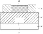
상기 박막 트랜지스터는 도 1과 같은 구조, 즉 기판(10) 상에 게이트 전극(20), 게이트 절연막(30), 채널층(50) 및 소스/드레인 전극(40)이 순차적으로 적층되어 있는 코-플래너형 구조의 하부 게이트 박막 트랜지스터로 구성될 수 있다.The thin film transistor has a structure as shown in FIG. 1, that is, a
상기 기판(10)으로는 이 분야의 일반적인 것이 사용될 수 있으며, 예를 들면, 유리, 금속호일, 플라스틱, 또는 실리콘 중에서 선택될 수 있다. 한편 플렉서블 기판에의 적용 가능성을 감안하면 상기 기판 재료들 중 플라스틱이 보다 바람직하다. As the
상기 게이트 전극(20)으로는 ITO, IZO, ZnO:Al(Ga) 등과 같은 투명 산화물, Ti, Ag, Au, Al, Cr, Al/Cr/Al, Ni등과 같은 여러 종류의 저항이 낮은 금속 또는 전도성 고분자가 사용될 수 있지만, 반드시 이것으로 제한되는 것은 아니다. 상기 게이트 전극(20)은 상기 기판(10) 상에 이 분야의 통상적인 두께로 스퍼터링법, 원자층 증착법(ALD), 화학기상 증착법(CVD) 등의 공정을 통해 증착된 후 패터닝될 수 있다.The
상기 기판(10)과 게이트 전극(20) 상에 형성되는 게이트 절연막(30)은 투명한 산화물 또는 질화물, 예를 들면 SiNx, AlON, TiO2, AlOx, TaOx, HfOx, SiON, SiOx 중 어느 하나 이상을 포함할 수 있으며, 바람직하게는 산화 알루미늄(Al2O3) 등이 사용될 수 있다. 그 이외에도 고분자를 이용한 박막도 적용 가능하다. 또한, 상기 게이트 절연막(30)은 이 분야의 통상적인 두께로 원자층 증착법(ALD), PECVD법, 기타 스퍼터링법과 같은 공정을 통해 형성될 수 있으며, 도시하지 않았지만 형성 후 전극 연결을 위한 패드가 형성될 수도 있다.The
상기 소스/드레인 전극(40) 및 채널 영역 상에 형성되는 채널층(50)은 주석 함유 산화물을 포함할 수 있다. 이 때 주석 함유 산화물은 SnO2의 유형으로 존재될 수 있다.The source /
다만 결정질 상태의 이산화 주석(SnO2)은 1020~1022/㎤ 정도로 매우 높은 전하 농도를 가진다. 결정질 상태의 이산화 주석은 채널층으로 사용하기에는 너무 높은 전기 전도도를 가지며 오히려 전극과 같은 전도성 소재에 적합하다. 따라서 이산화 주석이 채널층으로 사용되기 위해서는 먼저 전기 전도도가 채널층으로 사용되기에 적합할 정도로 조절되어야 한다. However, crystalline tin dioxide (SnO 2 ) has a very high charge concentration of about 10 20 ~ 10 22 / cm 3. Crystalline tin dioxide has an electrical conductivity that is too high for use as a channel layer, and is rather suitable for a conductive material such as an electrode. Therefore, in order for tin dioxide to be used as the channel layer, the electrical conductivity must first be adjusted to be suitable for use as the channel layer.
이에 따라 본 발명의 박막 트랜지스터는 전기 전도도 및/또는 결정성이 제어된 이산화 주석을 포함한다. 보다 구체적으로 본 발명의 박막 트랜지스터에서의 채널층은 알루미늄 도핑과 함께 상기 알루미늄의 도핑 위치를 제어함으로써 박막 트랜지스터의 전기적 특성을 개선시키는 것을 특징으로 한다. Accordingly, the thin film transistor of the present invention includes tin dioxide whose electrical conductivity and / or crystallinity is controlled. More specifically, the channel layer in the thin film transistor of the present invention is characterized by improving the electrical properties of the thin film transistor by controlling the doping position of the aluminum together with aluminum doping.
한편 상기 게이트 절연막(30)에 형성되는 소스·드레인 전극(40)으로는 게이트 전극(20)과 유사하게 ITO, IZO, ZnO:Al(Ga) 등의 투명 산화물, Al, Cr, Au, Ag, Ti 등의 금속 또는 전도성 고분자가 사용할 수 있지만 이것으로 제한되는 것은 아니다. 또한, 상기 소스·드레인 전극(40)은 상기 금속과 산화물의 이층구조를 형성할 수도 있다. 상기 소스/드레인 전극은 이 분야의 통상적인 두께로 스퍼터링법, ALD, CVD 등과 같은 공정을 통해 증착될 수 있다.On the other hand, as the source and drain
상기 채널층(50) 상에는 도시하지는 도 1에서 않았지만 보호층이 형성될 수 있다. 비한정적인 예로써 폴리이미드 폴리머와 같은 폴리머 물질들이 스핀 코팅, 딥코팅, 캐스팅 등과 같은 방법을 통해 형성된 후 패터닝 될 수 있다. 또한 SiO2, Al2O3와 같은 절연물질들이 화학증착법(CVD), 원자층 증착법(ALD) 등을 통해 형성된 후 패터닝 될 수 있다.Although not illustrated in FIG. 1 on the
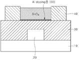
도 2는 본 발명의 일시예에 따른 도핑된 채널층을 포함하는 하부 게이트(bottom gate) 코-플래너(co-planar) 구조의 박막 트랜지스터의 단면도이다.2 is a cross-sectional view of a thin film transistor having a bottom gate co-planar structure including a doped channel layer according to an exemplary embodiment of the present invention.
이하 본 발명의 베이스 기판, 게이트 전극, 게이트 절연층, 및 소스 전극과 드레인 전극의 제조 방법과 적층 구조는 도 1의 박막 트랜지스터의 대응 구성과 동일하게 적용이 가능 한 바 이에 대한 자세한 설명은 생략한다. 이하에서는 본 발명의 주요 기술적 특징을 중심으로 해서 설명하도록 한다.Hereinafter, the manufacturing method and stacked structure of the base substrate, the gate electrode, the gate insulating layer, and the source electrode and the drain electrode can be applied in the same manner as the corresponding configuration of the thin film transistor of FIG. 1, and detailed description thereof will be omitted. . Hereinafter, description will be made focusing on the main technical features of the present invention.
도 2의 박막 트랜지스터는 도 1의 박막 트랜지스터와 대비할 때, 채널층(50)의 중간에 알루미늄 도핑층(60)을 추가로 포함하는 특징이 있다. 본 발명의 실시예의 알루미늄 도핑층(60)은 본 발명의 실시예의 박막 트랜지스터의 스위칭 소자로서의 전기적 특성을 개선하는 기능을 수행한다. The thin film transistor of FIG. 2 has a feature that additionally includes an aluminum doped
보다 구체적으로 본 발명의 실시예의 알루미늄 도핑층(60)은 이산화 주석 채널층(50)을 알루미늄으로 도핑시켜 스위칭 소자의 주요 특성인 온/오프 전류 비(on/off current ratio)를 향상시킬 수 있다. More specifically, the
또한 이산화 주석 채널층(50)은 도전성 재료에 상응하는 높은 전하 이동도를 가지므로 박막 트랜지스터의 채널층으로 사용하기 어렵다. 본 실시예의 알루미늄 도핑층(60)은 높은 전기 전도도를 가지는 이산화 주석 채널층(50)을 알루미늄으로 도핑시켜 채널층으로 사용할 수 있도록 전하 이동도(field effect mobility)를 감소시킬 수 있다.In addition, the tin
특히 본 발명의 실시예의 알루미늄 도핑층(60)은 이산화 주석 채널층(50)의 두께 방향으로 중간(1/2)에 위치하는 것이 바람직하다. 통상적으로 박막 트랜지스터는 증착 단계 이후 후속 공정으로 어닐링(annealing) 단계를 포함한다. 왜냐하면 박막 트랜지스터의 증착 단계에서도 양호한 증착막 품질을 위해 기판이 일정 온도 이상으로 가열되고 더 나아가 후속 공정에서도 확산(diffusion) 공정 등이 포함되기 때문이다. 만일 본 발명의 실시예의 알루미늄 도핑층(60)이 이산화 주석 채널층(50) 내에서 두께 방향으로 중간에 위치하게 되면, 알루미늄은 어닐링 공정 동안 이산화 주석 채널층(50)으로 확산되어 이산화 주석 채널층(50)의 결정화를 지연시킬 수 있다. 그 결과 이산화 주석 채널층(50)은 결정화가 되지 못하거나 완전한 결정화가 지연되어 전기 전도도가 감소되고 온/오프 전류 비가 높아질 수 있게 된다.In particular, the
한편 본 발명의 실시예의 알루미늄 도핑층(60)의 어닐링은 300~500℃의 온도 범위에서 수행되는 것이 바람직하다. 만일 어닐링 온도가 300℃ 보다 낮으면, 증착 직후의(as-dep) 비정질 상태의 주석 산화물(50)이 결정화(crystallization)되지 못하여 채널을 형성하지 못하게 되는 문제가 발생한다. 반면 어닐링 온도가 500℃ 보다 높으면, 주석 산화물층(50)으로 알루미늄과 갈륨(Ga)이 반도체 에너지 밴드 갭에서 shallow level로 들어가서 p-type 특성을 나타내어 결과적으로 트랜지스터의 특성을 저하시킬 수 있기 때문이다. Meanwhile, annealing of the aluminum doped
이하 본 발명의 구체적인 실험예를 토대로 더욱 상세히 설명하지만, 본 발명은 다음의 실험예에 의해 한정되거나 제한되는 것은 아니다.Hereinafter, the present invention will be described in more detail based on specific experimental examples, but the present invention is not limited or limited by the following experimental examples.
실시예Example
도 3은 본 발명의 일실시예인 도 2의 하부 게이트(bottom gate) 코-플래너(co-planar) 구조의 박막 트랜지스터의 제조 공정의 모식도이고, 도 4는 본 발명의 일실시예에 따른 도핑된 채널층을 형성하는 제조 공정의 모식도이다. 3 is a schematic diagram of a manufacturing process of a bottom gate co-planar structure of a thin film transistor of FIG. 2, which is an embodiment of the present invention, and FIG. 4 is doped according to an embodiment of the present invention. It is a schematic diagram of the manufacturing process of forming a channel layer.
먼저 100x100 ㎟의 알칼리성 없는 유리 기판을 아세톤, 이소-프로필 알콜 및 탈이온수로 순차적으로 초음파 세정하였다. 이어서, 세정된 유리 기판 상에 ITO를 가지고 DC-RF 마그네트론 스퍼터로 스퍼터링하여 150nm의 두께로 게이트 전극을 증착하고 패터닝하였다. 이어서 170nm 두께로 게이트 절연층을 알루미나를 사용하여 150℃에서 ALD법으로 형성하였다. 다음으로 도 3에서 도시하고 있는 바와 같이, PR층을 코팅한 후 채널층의 형상으로 패터닝한 후 도 2와 같은 본 발명의 일실시예에 따른 알루미늄이 도핑된(60) 이산화 주석 채널층(50)이 형성되었다.First, a 100 × 100 mm 3 alkali-free glass substrate was sequentially ultrasonically cleaned with acetone, iso-propyl alcohol and deionized water. Subsequently, a gate electrode was deposited and patterned to a thickness of 150 nm by sputtering with DC-RF magnetron sputtering with ITO on the cleaned glass substrate. Subsequently, a gate insulating layer having a thickness of 170 nm was formed by ALD method at 150 ° C using alumina. Next, as illustrated in FIG. 3, after coating the PR layer, patterning it into a shape of a channel layer, and then aluminum-doped (60) tin
도 2의 본 발명의 일실시예에 따른 이산화 주석 채널층(50)과 알루미늄 도핑층(60)의 형성 방법은 도 4에 자세히 도시되어 있다.The method of forming the tin
도 4를 참조하여, 본 발명의 일실시예의 이산화 주석 채널층(50)과 알루미늄 도핑층(60)은 원자층 증착법(ALD)으로 증착되었다. 보다 구체적으로 본 발명의 실시예에서의 원자층 증착법은 주석 산화물(SnOx) 사이클/아르곤(Ar) 퍼징/알루미늄 산화물(Al2O3) 사이클/아르곤 퍼징 단계를 포함한다. Referring to FIG. 4, the tin
이 때 상기 주석 산화물(SnOx) 사이클은 원하는 이산화 주석 채널층(50)의 두께에 따라 수십~수백 회 반복되었다. 반면 알루미늄 산화물(Al2O3) 사이클은 1회 수행되었다. 그러나 상기 알루미늄 산화물(Al2O3) 사이클은 원하는 알루미늄 도핑층의 두께에 따라 1 내지 수회 수행될 수 있다. At this time, the tin oxide (SnO x ) cycle was repeated tens to hundreds of times depending on the thickness of the desired tin
또한 상기 알루미늄 산화물(Al2O3) 사이클이 적용되는 순서는 알루미늄 도핑층(60)의 이산화 주석 채널층(50) 내의 위치에 따라 결정된다. 일례로 도 2에 도시된 본 발명의 일실시예와 같이 알루미늄 도핑층(60)이 이산화 주석 채널층(50) 가운데 위치하면, 알루미늄 산화물(Al2O3) 사이클은 전체 주석 산화물(SnOx) 사이클 횟수의 중간에 위치한다. 반면 후술할 비교예에서와 같이 알루미늄 도핑층(60)이 이산화 주석 채널층(50)의 두께 방향으로 1/4 또는 3/4에서 위치한다면, 알루미늄 산화물(Al2O3) 사이클은 전체 주석 산화물(SnOx) 사이클 횟수의 각각 1/4 또는 3/4 부근에 위치한다. In addition, the order in which the aluminum oxide (Al 2 O 3 ) cycle is applied is determined according to the position in the tin
한편 상기 주석 산화물(SnOx) 사이클은 원자층 증착법(ALD)을 이용하며 각 단계는 다시 주석 화학종을 공급하여 기판 위에 주석 화학종을 흡착시키는 단계/아르곤 퍼징 단계/산소 원을 공급하여 주석 화학종이 흡착된 기판 위에 산소 화학종을 흡착시켜 산화 반응을 일으키는 단계/아르곤 퍼징 단계를 포함한다.Meanwhile, the tin oxide (SnO x ) cycle uses atomic layer deposition (ALD), and each step again supplies tin chemicals to adsorb tin chemicals on the substrate / argon purging step / oxygen source to supply tin chemicals The step of adsorbing oxygen species on the adsorbed substrate causes an oxidation reaction / argon purging step.
이 때 상기 주석 화학종은 4가의 주석 전구체가 바람직하다. 비한정적인 구체적인 예로써 주석 전구체는 tetrakis(dimethylamino)tin (TDMASn)를 포함할 수 있고 상기 산소 화학종은 오존, 산소 등을 포함할 수 있으나, 이에 반드시 한정되는 것은 아니다.In this case, the tin species is preferably a tetravalent tin precursor. As a non-limiting specific example, the tin precursor may include tetrakis (dimethylamino) tin (TDMASn), and the oxygen species may include ozone, oxygen, etc., but is not limited thereto.
한편 알루미늄 산화물(Al2O3) 사이클은 본 기술 분야의 통상의 지식을 가진 자에게 알려진 것으로 적용이 가능 한 바 이에 대한 자세한 설명은 생략한다.Meanwhile, the aluminum oxide (Al 2 O 3 ) cycle is known to those skilled in the art and can be applied. Therefore, detailed description thereof will be omitted.
다시 도 3으로 돌아가서 도 4의 방법으로 채널층 및 알루미늄 도핑층을 증착한 후 상기 PR을 리프트 오프하면, 알루미늄 도핑층(60)을 포함하는 이산화 주석 채널층(50)이 형성된다.Returning to FIG. 3 again, after depositing the channel layer and the aluminum doping layer in the method of FIG. 4 and lifting the PR off, a tin
이후 후속 공정으로 ITO을 가지고 DC-RF 마그네트론 스퍼터로 스퍼터링하여 150nm의 두께로 소스/드레인 전극을 증착 및 패터닝(또는 패터닝 및 증착)하여 형성하였다. 상기 스퍼터링은 0.2Pa의 챔버 압력과 300W의 스퍼터링 파워를 가지고 Ar/O2 분위기에서 수행하였으며, 모든 패터닝은 포토-리소그래피 방법 및 습식 식각 방법으로 수행하였다. 상기 공정 조건은 본 기술 분야의 통상의 지식을 가진 자에게 알려진 것으로 장비 및 소자의 특성에 따라 변경하여 적용이 가능함은 자명하다.Subsequently, it was formed by depositing and patterning (or patterning and depositing) the source / drain electrodes with a thickness of 150 nm by sputtering with DC-RF magnetron sputtering with ITO as a subsequent process. The sputtering was performed in an Ar / O 2 atmosphere with a chamber pressure of 0.2 Pa and a sputtering power of 300 W, and all patterning was performed by a photo-lithography method and a wet etching method. It is obvious that the above process conditions are known to those skilled in the art and can be applied by changing the characteristics of equipment and devices.
상기와 같은 공정에 의해 형성된 본 발명의 일실시예에 따른 박막 트랜지스터는 후속 공정으로 어닐링 처리된 후 특성 평가(도 7 내지 10) 및 XRD 분석(도 11 내지 14) 되었다.The thin film transistor according to an embodiment of the present invention formed by the above process was subjected to annealing treatment in a subsequent process (Figures 7 to 10) and XRD analysis (Figures 11 to 14).
비교예 1Comparative Example 1
알루미늄 도핑층(60)이 이산화 주석 채널층(50)의 두께 방향으로 3/4에서 위치하는 것만을 제외하고 실시예 1과 동일하게 하여 박막 트랜지스터 소자를 제작하였다. 다시 말하면 도 4의 알루미늄 산화물(Al2O3) 사이클이 전체 주석 산화물(SnOx) 사이클 횟수의 3/4 부근에 위치하는 것만을 제외하고 실시예 1과 동일한 조건에서 비교예 1의 박막 트랜지스터 소자가 제작되었다.A thin film transistor device was manufactured in the same manner as in Example 1, except that the aluminum doped
이어서 본 발명의 비교예 1에 따른 박막 트랜지스터는 후속 공정으로 어닐링 처리된 후 특성 평가(도 7 내지 10) 및 XRD 분석(도 11 내지 14) 되었다.Subsequently, the thin film transistor according to Comparative Example 1 of the present invention was subjected to annealing treatment in a subsequent process (Figs. 7 to 10) and XRD analysis (Figs. 11 to 14).
비교예 2Comparative Example 2
알루미늄 도핑층(60)이 이산화 주석 채널층(50)의 두께 방향으로 1/4에서 위치하는 것만을 제외하고 실시예 1과 동일하게 하여 박막 트랜지스터 소자를 제작하였다. 다시 말하면 도 4의 알루미늄 산화물(Al2O3) 사이클이 전체 주석 산화물(SnOx) 사이클 횟수의 1/4 부근에 위치하는 것만을 제외하고 실시예 1과 동일한 조건에서 비교예 1의 박막 트랜지스터 소자가 제작되었다.A thin film transistor device was manufactured in the same manner as in Example 1, except that the aluminum doped
이어서 본 발명의 비교예 2에 따른 박막 트랜지스터는 후속 공정으로 어닐링 처리된 후 특성 평가(도 7 내지 10) 및 XRD 분석(도 11 내지 14) 되었다.Subsequently, the thin film transistor according to Comparative Example 2 of the present invention was subjected to annealing treatment in a subsequent process (Figs. 7 to 10) and XRD analysis (Figs. 11 to 14).
박막 트랜지스터의 특성 평가Evaluation of characteristics of thin film transistors
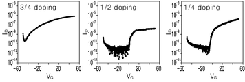
도 7 내지 10은 각각 본 발명의 실시예(1/2 위치 도핑층)와 비교예들(1/4 또는 3/4 위치 도핑층)에 따라 증착 직후(as-dep) 또는 300~500℃에서 어닐링된 박막 트랜지스터의 전류-전압 특성을 나타낸 그래프이다. 7 to 10, respectively, according to an embodiment of the present invention (1/2 position doping layer) and comparative examples (1/4 or 3/4 position doping layer) immediately after deposition (as-dep) or at 300 to 500 ° C. It is a graph showing the current-voltage characteristics of the annealed thin film transistor.
먼저 증착 직후(as-dep) 본 발명의 실시예 및 비교예들에 따른 박막 트랜지스터는 전류-전압 특성은 도 7과 같이 측정되었고 그 결과는 아래의 표와 같이 정리된다.First, immediately after deposition (as-dep), the current-voltage characteristics of the thin film transistor according to the embodiments and comparative examples of the present invention were measured as shown in FIG. 7 and the results are summarized as in the table below.
<표> 도핑 위치별 As-dep SnO<Table> As-dep SnO by doping position 22 :Al 소자 I-V 특성: Al device I-V characteristics

증착 직후(As-dep) 상태에서의 SnO2:Al(알루미늄 도핑 주석 산화물) 채널층을 포함하는 소자의 I-V 특성 결과는 먼저 두께 1/4(비교예 1)와 3/4(비교예 2) 위치의 도핑에서 유사한 온/오프 전류 특성을 가짐을 알 수 있다. 이와는 반대로 1/2(실시예) 도핑에서는 온/오프 전류 특성이 떨어지는 것을 알 수 있다.The IV characteristic results of the device including the SnO 2 : Al (aluminum doped tin oxide) channel layer in the immediately after deposition (As-dep) state are firstly 1/4 (Comparative Example 1) and 3/4 (Comparative Example 2). It can be seen that the doping of the position has similar on / off current characteristics. On the contrary, it can be seen that in the doping of 1/2 (example), the on / off current characteristics are poor.
상기와 같은 비교예들의 박막 트랜지스터의 전기적 특성은 채널을 형성할 때 두께 1/4와 3/4 위치의 알루미늄 도핑 영역이 아닌 비정질의 SnO2 부분의 영역에서 채널(전하농도 = 1016~1018/㎤)이 형성되었기 때문인 것으로 추정된다. 반면 상기 실시예의 박막 트랜지스터의 전기적 특성은 알루미늄 도핑층의 방해로 인해 채널을 형성하지 못하고 또한 전하의 이동이 쉽지 않게 되어 그 결과 온/오프 전류 비와 전하 이동도(field effect mobility)가 감소한 것으로 추정된다.The electrical characteristics of the thin film transistors of the above comparative examples are channels (charge concentration = 10 16 ~ 10 18) in the region of the amorphous SnO 2 portion, rather than the aluminum doped regions at the 1/4 and 3/4 thicknesses when forming the channel. / Cm3) is assumed to be formed. On the other hand, the electrical properties of the thin film transistor of the above embodiment are estimated to have reduced the on / off current ratio and the field effect mobility as a result of the fact that the channel cannot be formed due to the interference of the aluminum doping layer and the charge is not easily moved. do.
이와는 달리 300~500℃ 대기(air) 어닐링 후 본 발명의 실시예 및 비교예들에 따른 박막 트랜지스터는 전류-전압 특성은 도 8 내지 10과 같이 측정되었고 그 결과는 아래의 표들과 같이 정리된다.On the contrary, the current-voltage characteristics of the thin film transistors according to embodiments and comparative examples of the present invention after 300 to 500 ° C. air annealing were measured as shown in FIGS. 8 to 10 and the results are summarized as in the following tables.
<표> 도핑 위치별 300℃ 대기(air) 어닐링된 SnO<Table> 300 ° C air annealed SnO by doping position 22 :Al 소자 I-V 특성: Al device I-V characteristics

<표> 도핑 위치별 400℃ 대기(air) 어닐링된 SnO<Table> 400 ° C air annealed SnO by doping position 22 :Al 소자 I-V 특성: Al device I-V characteristics

<표> 도핑 위치별 500℃ 대기(air) 어닐링된 SnO<Table> 500 ° C air annealed SnO by doping position 22 :Al 소자 I-V 특성: Al device I-V characteristics

먼저 300~500℃에서 어닐링된 비교예들의 박막 트랜지스터의 전기적 특성은 모두 증착 직후(as-dep)의 결과와는 반대로 온/오프 전류 비 특성이 저하되었다. 비교예들의 박막 트랜지스터의 상기 특성 저하는 어닐링으로 인해 이산화 주석(SnO2)이 안정한 상(phase)인 결정상으로 상변태 되었기 때문인 것으로 추정된다.First, all of the electrical properties of the thin film transistors of the comparative examples annealed at 300 to 500 ° C., as opposed to the result of immediately after deposition (as-dep), had a decrease in the on / off current ratio property. It is presumed that tin dioxide (SnO 2 ) was transformed into a stable phase crystal phase due to annealing due to the annealing.
반면 비교예들과는 달리 300~500℃에서 어닐링된 본 발명의 실시예의 박막 트랜지스터에서는 온/오프 전류 비가 스위칭 소자로 사용하기에 충분한 정도로 증가한 것으로 측정되었다. 본 발명의 실시예의 박막 트랜지스터에서의 상기 특성 향상은 1/2 위치의 알루미늄 도핑층이 SnO2:Al SnO2:Al(알루미늄 도핑 주석 산화물) 채널에서 결정화를 방해하여 스위칭 소자로 사용하기에 적절한 1016~1018/㎤ 수준의 전하농도 영역에서 채널을 형성하는 것에서 기인한 것으로 추정된다.On the other hand, unlike the comparative examples, in the thin film transistor of the embodiment of the present invention annealed at 300 to 500 ° C, it was measured that the on / off current ratio increased to a degree sufficient to be used as a switching element. The improvement of the characteristics in the thin film transistor of the embodiment of the present invention is that the aluminum doped layer at the 1/2 position interferes with crystallization in the SnO 2 : Al SnO 2 : Al (aluminum doped tin oxide) channel and is suitable for use as a switching element. It is presumed to be due to the formation of a channel in the region of the charge concentration of 16 to 10 18 / cm 3.
한편 본 명세서에서 기재하지는 않았으나 200℃에서 어닐링 된 1/2 위치의 알루미늄 도핑층을 포함하는 SnO2:Al(알루미늄 도핑 주석 산화물) 채널층의 박막 트랜지스터는 도 7의 증착 직후(As-dep) 상태의 1/2 위치의 알루미늄 도핑층을 포함하는 SnO2:Al(알루미늄 도핑 주석 산화물) 채널층의 박막 트랜지스터와 동일하게 온/오프 전류 특성이 떨어지는 것으로 측정되었다. 이는 200℃ 어닐링시 주석 화학종인 주석 전구체와 산소 화학종의 반응으로 형성되는 주석 산화물이 너무 낮은 어닐링 온도로 인해 결정을 형성하지 못하기 때문인 것으로 추정된다.On the other hand, although not described herein, the thin film transistor of the SnO 2 : Al (aluminum doped tin oxide) channel layer including the aluminum doped layer at the 1/2 position annealed at 200 ° C is immediately after deposition (As-dep) of FIG. 7. It was measured that the on / off current characteristics were inferior to those of the thin film transistor of the SnO 2 : Al (aluminum doped tin oxide) channel layer including the aluminum doped layer at 1/2 position of. This is presumed to be due to the fact that the tin oxide formed by the reaction of the tin precursor, which is a tin species, and the oxygen species, during annealing at 200 ° C does not form crystals due to an annealing temperature that is too low.
또한 본 명세서에서 기재하지는 안았으나 550℃에서 어닐링 된 1/2 위치의 알루미늄 도핑층을 포함하는 SnO2:Al(알루미늄 도핑 주석 산화물) 채널층의 박막 트랜지스터는 도 8 내지 10의 300~500℃에서 어닐링된 1/4 및 3/4 위치의 알루미늄 도핑층을 포함하는 SnO2:Al(알루미늄 도핑 주석 산화물) 채널층의 박막 트랜지스터와 동일하게 온/오프 전류 특성이 떨어지는 것으로 측정되었다. 550℃ 어닐링은 알루미늄의 주석 산화물층(50)으로 알루미늄과 갈륨(Ga)이 반도체 에너지 밴드 갭에서 shallow level로 들어가서 p-type 특성을 나타내어 트랜지스터의 특성을 저하시키기 때문인 것으로 추정된다.Also, although not described in this specification, the thin film transistor of the SnO 2 : Al (aluminum doped tin oxide) channel layer including the aluminum doped layer at 1/2 position annealed at 550 ° C is 300 to 500 ° C in FIGS. 8 to 10. It was measured that the on / off current characteristics were inferior to those of the thin film transistor of the SnO 2 : Al (aluminum doped tin oxide) channel layer including the annealed aluminum doped layers at 1/4 and 3/4 positions. It is presumed that the annealing at 550 ° C. is a
XRD 평가XRD evaluation
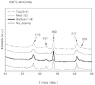
상기와 같은 본 발명의 실시예(1/2 위치 도핑층)와 비교예들(1/4 또는 3/4 위치 도핑층)에 따른 박막 트랜지스터의 전류-전압 특성에 대한 원인을 파악하기 위해, SnO2:Al(알루미늄 도핑 주석 산화물) 채널층의 결정성 분석이 XRD를 통해 수행되었다.In order to determine the cause of the current-voltage characteristics of the thin film transistor according to the embodiment of the present invention (1/2 position doping layer) and comparative examples (1/4 or 3/4 position doping layer) as described above, SnO 2 : Crystallinity analysis of the Al (aluminum doped tin oxide) channel layer was performed via XRD.
도 11 내지 14는 각각 본 발명의 실시예(1/2 위치 도핑층)와 비교예들(1/4 또는 3/4 위치 도핑층)에 따른 SnO2:Al(알루미늄 도핑 주석 산화물) 채널층의 증착 후 및 300~500℃에서 대기(air) 어닐링된(as-annealed) XRD 결과이다.11 to 14 are SnO 2 : Al (aluminum doped tin oxide) channel layers according to embodiments (1/2 position doping layer) and comparative examples (1/4 or 3/4 position doping layer) of the present invention, respectively. It is the result of XRD after air deposition and as-annealed at 300 ~ 500 ° C.
먼저 도 11에서 보여주는 바와 같이, 증착 직후(as-dep) 본 발명의 실시예와 비교예들의 SnO2:Al(알루미늄 도핑 주석 산화물) 채널층뿐만 아니라 도핑되지 않은 주석 산화물층(SnO2)은 모두 비정질(amorphous) 구조를 가지는 것으로 나타났다.First, as shown in FIG. 11, both the undoped tin oxide layer (SnO 2 ) as well as the SnO 2 : Al (aluminum doped tin oxide) channel layer of the embodiments and comparative examples of the present invention immediately after deposition (as-dep). It has been shown to have an amorphous structure.
반면 후속 어닐링 공정은 발명의 실시예와 비교예들의 SnO2:Al(알루미늄 도핑 주석 산화물) 채널층뿐만 아니라 도핑되지 않은 주석 산화물층(SnO2)의 결정구조를 크게 변화시킨다. On the other hand, the subsequent annealing process significantly changes the crystal structure of the undoped tin oxide layer (SnO 2 ) as well as the SnO 2 : Al (aluminum doped tin oxide) channel layer of the inventive examples and comparative examples.
먼저 본 발명의 실시예와 비교예들의 SnO2:Al(알루미늄 도핑 주석 산화물) 채널층과 도핑되지 않은 주석 산화물(SnO2)층은 모두 300~500℃의 후속 어닐링 공정에 의해 결정성을 나타내고 있음을 도 12 내지 14를 통해 알 수 있다. 또한 도핑되지 않은 주석 산화물(SnO2) 및 SnO2:Al(알루미늄 도핑 주석 산화물)의 결정 구조는 모두 rutile 결정 구조를 가지는 것으로 측정되었다.First, both the SnO 2 : Al (aluminum doped tin oxide) channel layer and the undoped tin oxide (SnO 2 ) layer of the examples and comparative examples of the present invention show crystallinity by a subsequent annealing process at 300 to 500 ° C. It can be seen through Figures 12 to 14. In addition, the crystal structures of undoped tin oxide (SnO 2 ) and SnO 2 : Al (aluminum doped tin oxide) were all measured to have rutile crystal structures.
그러나 본 발명의 실시예의 채널층 두께 1/2 위치의 알루미늄 도핑에서는 rutile 구조의 XRD의 반치 전폭(full width half maximum: FWHM)은 본 발명의 비교예들 또는 도핑되지 않은 주석 산화물(SnO2) 대비 보다 넓은 경향을 가짐을 도 12 내지 14를 통해 알 수 있다. However, in the aluminum doping at the position of 1/2 of the channel layer thickness in the embodiment of the present invention, the full width half maximum (FWHM) of the XRD of the rutile structure is compared with the comparative examples of the present invention or undoped tin oxide (SnO 2 ). It can be seen from FIGS. 12 to 14 that it has a broader tendency.
아래의 표는 본 발명의 비교예들인 채널층 두께 1/4과 3/4 위치에서 도핑되고 후속 어닐링된 SnO2:Al(알루미늄 도핑 주석 산화물) 박막과 본 발명의 실시예인 채널층 두께 1/2 위치에서 도핑되고 후속 어닐링된 SnO2:Al(알루미늄 도핑 주석 산화물) 박막의 (200)면 기준의 XRD의 반치 전폭 측정 결과를 요약한 것이다.The following table shows the comparative example of the present invention, the
<표> 대기(air) 어닐링에 따른 (200)면 기준 XRD 반치 전폭<Table> XRD half width at (200) plane according to air annealing

본 발명의 실시예인 채널층 두께 1/2 위치에서 도핑된 SnO2:Al(알루미늄 도핑 주석 산화물) 박막은 비교예들인 채널층 두께 1/4과 3/4 위치에서 도핑된 SnO2:Al(알루미늄 도핑 주석 산화물) 박막보다 XRD 반치 전폭이 전체 어닐링 온도 범위에서 최소 40% 이상 큰 것을 상기 표의 측정 결과로부터 알 수 있다. 또한 본 발명의 실시예인 채널층 두께 1/2 위치에서 도핑된 SnO2:Al(알루미늄 도핑 주석 산화물) 박막은 도핑되지 않은 주석 산화물(SnO2) 보다 XRD 반치 전폭이 전체 어닐링 온도 범위에서 160% 내지 213% 이상 큰 것을 상기 표의 측정 결과로부터 알 수 있다.Doped
상기 XRD 반치 전폭 결과는 본 발명의 실시예의 채널층 두께 1/2 위치의 도핑 후 어닐링된 박막의 결정성이 비교예들 및 도핑되지 않은 주석 산화물(SnO2)층 대비 떨어진다는 의미이다. 본 발명의 실시예의 결정성 저하는 도핑된 알루미늄이 어닐링으로 인해 SnO2 내부로 확산되어 SnO2의 결정화를 방해하였기 때문인 것으로 판단된다. 본 발명의 실시예의 상기 낮은 결정성은 상기 I-V 분석에서 어닐링된 본 발명의 실시예의 채널층을 가지는 소자의 온/오프 전류 비가 확보될 수 있었던 이유들 중 하나인 것으로 판단된다.The XRD half width full width result means that the crystallinity of the annealed thin film after doping at the position of 1/2 of the thickness of the channel layer in the embodiment of the present invention is inferior to that of comparative examples and the undoped tin oxide (SnO 2 ) layer. Embodiment of the invention is the crystalline deterioration due to the doped aluminum annealing diffuses into the SnO 2 is judged to be due to interference hayeotgi crystallization of SnO 2. The low crystallinity of the embodiment of the present invention is considered to be one of the reasons why the on / off current ratio of the device having the channel layer of the embodiment of the present invention annealed in the IV analysis could be secured.
반면 본 발명의 비교예들인 채널층 두께 1/4과 3/4 위치에서 도핑되고 후속 어닐링된 SnO2:Al(알루미늄 도핑 주석 산화물) 박막은 본 발명의 실시예 대비 상기 XRD 반치 전폭이 더 작은 것으로 측정되었다. 이는 다시 본 발명의 비교예들의 SnO2:Al(알루미늄 도핑 주석 산화물) 박막은 높은 결정성을 가지는 것을 의미한다. On the other hand, the comparative examples of the present invention, the SnO 2 : Al (aluminum doped tin oxide) thin film doped at
이산화 주석(SnO2)은 높은 결정성을 가질수록 높은 전하 농도(1020~1022/㎤)를 가진다. 이와 같은 정도의 전하 농도를 가지는 박막은 현재 투명전도막으로 널리 사용되는 ITO가 가지는 전하 농도와 유사한 수준이므로 박막 트랜지스터 소자로 사용되기에는 부적합하다.The higher the crystallinity of tin dioxide (SnO 2 ), the higher the charge concentration (10 20 ~ 10 22 / cm 3). A thin film having a charge concentration of such a degree is not suitable for use as a thin film transistor device because it is similar to the charge concentration of ITO, which is widely used as a transparent conductive film.
이상에서는 본 발명의 실시예를 중심으로 설명하였지만, 통상의 기술자의 수준에서 다양한 변경이나 변형을 가할 수 있다. 따라서, 이러한 변경과 변형이 본 발명의 범위를 벗어나지 않는 한 본 발명의 범주 내에 포함되는 것으로 이해될 수 있을 것이다.In the above, the description has been mainly focused on the embodiment of the present invention, but various changes or modifications can be made at the level of a person skilled in the art. Accordingly, it will be understood that such changes and modifications are included within the scope of the present invention without departing from the scope of the present invention.
10: 기판
20: 게이트 전극
30: 게이트 절연막
40: 소스/드레인 전극
50: 채널층
60: 알루미늄 도핑층10: substrate 20: gate electrode
30: gate insulating film 40: source / drain electrode
50: channel layer 60: aluminum doping layer
Claims (11)
상기 베이스 기판 상에 위치하는 게이트 전극;
상기 게이트 전극 상에 위치하는 게이트 절연층;
상기 게이트 절연층 상에 위치하는 채널층;
상기 게이트 절연층 상에 위치하며 상기 채널층을 사이에 두고 상호 이격된 소스 전극과 드레인 전극;을 포함하고,
상기 채널층은 알루미늄이 도핑된 이산화 주석을 포함하며, 전하농도가 1016~1018/㎤인 것;을 특징으로 하는 박막 트랜지스터.
Base substrate;
A gate electrode positioned on the base substrate;
A gate insulating layer on the gate electrode;
A channel layer positioned on the gate insulating layer;
Included on the gate insulating layer and the source layer and the drain electrode spaced apart from each other with the channel layer therebetween;
The channel layer includes tin dioxide doped with aluminum, and has a charge concentration of 10 16 ~ 10 18 / cm 3; thin film transistor.
상기 박막 트랜지스터는 전하 이동도(field effect mobility)가 0.1~4 ㎠/Vs인 것;을 특징으로 하는 박막 트랜지스터.
According to claim 1,
The thin film transistor is characterized in that the charge mobility (field effect mobility) is 0.1 ~ 4 ㎠ / Vs; thin film transistor.
상기 박막 트랜지스터는 온/오프 전류 비가 (1~10)*106 인 것;을 특징으로 하는 박막 트랜지스터.
According to claim 1,
The thin film transistor has an on / off current ratio of (1 to 10) * 10 6 .
상기 채널층의 대기(air) 어닐링 후 XRD 반치 전폭(full width half maximum)은 (200)면 피크를 기준으로 도핑되지 않은 주석 산화물(SnO2)의 대기 어닐링 후 XRD 반치 전폭보다 1.6배 내지 2.13배 큰 것;을 특징으로 하는 박막 트랜지스터.
According to claim 1,
After air annealing of the channel layer, the full width half maximum of XRD is 1.6 to 2.13 times than the full width of XRD half after atmospheric annealing of undoped tin oxide (SnO 2 ) based on the (200) plane peak. A thin film transistor characterized by being large.
상기 게이트 전극 상에 게이트 절연층을 형성하는 공정;
상기 게이트 절연층 상에 채널층을 형성하는 공정;
상기 게이트 절연층 상에 위치하며 상기 채널층을 사이에 두고 상호 이격된 소스 전극과 드레인 전극을 형성하는 공정;
어닐링 공정;을 포함하고,
상기 채널층을 형성하는 공정은 주석 산화물(SnOx) 사이클/아르곤(Ar) 퍼징/알루미늄 산화물(Al2O3) 사이클/아르곤 퍼징 단계를 포함하며, 상기 알루미늄 산화물(Al2O3) 사이클은 복수 회 수행되는 주석 산화물(SnOx) 사이클의 중간 단계에 수행되는 것;을 특징으로 하는 박막 트랜지스터의 제조 방법.
Forming a gate electrode on the substrate;
Forming a gate insulating layer on the gate electrode;
Forming a channel layer on the gate insulating layer;
Forming a source electrode and a drain electrode spaced apart from each other with the channel layer interposed therebetween;
Including an annealing process;
The process of forming the channel layer includes a tin oxide (SnO x ) cycle / argon (Ar) purging / aluminum oxide (Al 2 O 3 ) cycle / argon purging step, and the aluminum oxide (Al 2 O 3 ) cycle is Method of manufacturing a thin film transistor characterized in that it is performed in the intermediate step of the tin oxide (SnO x ) cycle is performed multiple times.
상기 주석 산화물(SnOx) 사이클은 원자층 증착법(ALD)을 이용하며, 각 단계는 주석 화학종을 공급하여 기판 위에 주석 화학종을 흡착시키는 단계/아르곤 퍼징 단계/산소 원을 공급하여 주석 화학종이 흡착된 기판 위에 산소 화학종을 흡착시켜 산화 반응을 일으키는 단계/아르곤 퍼징 단계를 포함하는 것;을 특징으로 하는 박막 트랜지스터의 제조 방법.
The method of claim 5,
The tin oxide (SnO x ) cycle uses atomic layer deposition (ALD), and each step supplies a tin chemical species to adsorb tin chemicals onto the substrate / argon purging step / provides an oxygen source to supply the tin chemical paper A method of manufacturing a thin film transistor comprising: argon purging step / step of causing an oxidation reaction by adsorbing oxygen species on the adsorbed substrate.
상기 주석 화학종은 4가 주석 전구체를 포함하고, 상기 산소 원은 오존 또는 산소인 것;을 특징으로 하는 박막 트랜지스터의 제조 방법.
The method of claim 6,
The tin species includes a tetravalent tin precursor, and the oxygen source is ozone or oxygen.
상기 어닐링 공정은 대기(air)에서 300~500℃ 온도범위에서 수행되는 것; 을 특징으로 하는 박막 트랜지스터의 제조 방법.
The method of claim 5,
The annealing process is carried out in an air (300) to 500 ℃ temperature range; Method of manufacturing a thin film transistor, characterized in that.
상기 어닐링 공정 후 상기 채널층의 전하농도는 1016~1018/㎤인 것;을 특징으로 하는 박막 트랜지스터의 제조 방법.
The method of claim 8,
After the annealing process, the charge concentration of the channel layer is 10 16 ~ 10 18 / cm 3; method of manufacturing a thin film transistor.
상기 어닐링 공정 후 상기 박막 트랜지스터의 전하 이동도(field effect mobility)는 0.1~4 ㎠/Vs이고, 온/오프 전류 비는 (1~10)*106 인 것;을 특징으로 하는 박막 트랜지스터의 제조 방법.
The method of claim 8,
After the annealing process, the thin film transistor has a charge effect (field effect mobility) of 0.1 to 4 cm 2 / Vs, and an on / off current ratio of (1 to 10) * 10 6 ; Way.
상기 어닐링 공정 후 상기 채널층의 XRD 반치 전폭(full width half maximum)은 (200)면 피크를 기준으로 도핑되지 않은 주석 산화물(SnO2)의 XRD 반치 전폭보다 1.6배 내지 2.13배 큰 것;
을 특징으로 하는 박막 트랜지스터의 제조 방법.
The method of claim 8,
After the annealing process, the full width half maximum of the channel layer is 1.6 to 2.13 times larger than the full width of the XRD half of the undoped tin oxide (SnO 2 ) based on the (200) plane peak;
Method of manufacturing a thin film transistor, characterized in that.
Priority Applications (2)
| Application Number | Priority Date | Filing Date | Title |
|---|---|---|---|
| KR1020180141672A KR20200057372A (en) | 2018-11-16 | 2018-11-16 | DOPED TIN OXIDE THIN FILE TRANSISTOR and manufacturing method thereof |
| PCT/KR2019/011723 WO2020101164A1 (en) | 2018-11-16 | 2019-09-10 | Doped tin oxide thin film transistor and method for manufacturing same |
Applications Claiming Priority (1)
| Application Number | Priority Date | Filing Date | Title |
|---|---|---|---|
| KR1020180141672A KR20200057372A (en) | 2018-11-16 | 2018-11-16 | DOPED TIN OXIDE THIN FILE TRANSISTOR and manufacturing method thereof |
Publications (1)
| Publication Number | Publication Date |
|---|---|
| KR20200057372A true KR20200057372A (en) | 2020-05-26 |
Family
ID=70732189
Family Applications (1)
| Application Number | Title | Priority Date | Filing Date |
|---|---|---|---|
| KR1020180141672A KR20200057372A (en) | 2018-11-16 | 2018-11-16 | DOPED TIN OXIDE THIN FILE TRANSISTOR and manufacturing method thereof |
Country Status (2)
| Country | Link |
|---|---|
| KR (1) | KR20200057372A (en) |
| WO (1) | WO2020101164A1 (en) |
Family Cites Families (2)
| Publication number | Priority date | Publication date | Assignee | Title |
|---|---|---|---|---|
| KR101608887B1 (en) * | 2009-04-17 | 2016-04-05 | 삼성전자주식회사 | Inverter, method of manufacturing the same and logic circuit comprising inverter |
| JP2018022879A (en) * | 2016-07-20 | 2018-02-08 | 株式会社リコー | Field-effect transistor, method for manufacturing the same, display element, image display device, and system |
-
2018
- 2018-11-16 KR KR1020180141672A patent/KR20200057372A/en active IP Right Grant
-
2019
- 2019-09-10 WO PCT/KR2019/011723 patent/WO2020101164A1/en active Application Filing
Also Published As
| Publication number | Publication date |
|---|---|
| WO2020101164A1 (en) | 2020-05-22 |
Similar Documents
| Publication | Publication Date | Title |
|---|---|---|
| US8026506B2 (en) | Thin-film transistor with channel layer formed by metal oxide film including indium, and method of manufacturing the same | |
| KR101638978B1 (en) | Thin film transistor and manufacturing method of the same | |
| KR100785038B1 (en) | Amorphous ZnO based Thin Film Transistor | |
| KR101980196B1 (en) | Transistor, method of manufacturing the same and electronic device including transistor | |
| US8084307B2 (en) | Method for manufacturing thin film transistor | |
| JP6338361B2 (en) | Semiconductor material, thin film transistor including the same, and electronic device including the thin film transistor | |
| US9087907B2 (en) | Thin film transistor and method of manufacturing the same | |
| KR100918404B1 (en) | Organic thin film transistor and a flat panel display employing the same | |
| KR100857455B1 (en) | Method of fabricating thin film transistor including ald deposited protection layer on the oxide semiconductor | |
| TWI405335B (en) | Semiconductor structure and fabricating method thereof | |
| US20120037897A1 (en) | Thin film transistor and method for manufacturing thin film transistor | |
| TW200937534A (en) | Method for manufacturing field-effect transistor | |
| KR20080052107A (en) | Filed-effect thin film transistor including a oxidized semiconductor | |
| KR20110028385A (en) | Treatment of gate dielectric for making high performance metal oxide and metal oxynitride thin film transistors | |
| KR101975929B1 (en) | Transistor having oxynitride channel layer and method of manufacturing the same | |
| JP2010123913A (en) | Thin-film transistor and method of manufacturing the same | |
| KR102144992B1 (en) | Semiconductor material, transistor including semiconductor material and electronic device including transistor | |
| US10396187B2 (en) | Semiconductor device | |
| KR101417932B1 (en) | Thin film transistor having double layered semiconductor channel and method of manufacturing the thin film transistor | |
| KR101876011B1 (en) | Oxide thin film transistor and method of manufacturing the same | |
| JP2011258804A (en) | Field effect transistor and manufacturing method therefor | |
| KR20160060848A (en) | Thin film transistor and Method of manufacturing the same | |
| KR20200057372A (en) | DOPED TIN OXIDE THIN FILE TRANSISTOR and manufacturing method thereof | |
| JP5553868B2 (en) | Display device using oxide semiconductor and manufacturing method thereof | |
| KR102000829B1 (en) | Thin Film Transistor Including a High-k Insulating Thin Film and Method for Manufacturing The Same |
Legal Events
| Date | Code | Title | Description |
|---|---|---|---|
| E902 | Notification of reason for refusal | ||
| AMND | Amendment | ||
| E601 | Decision to refuse application | ||
| X091 | Application refused [patent] | ||
| AMND | Amendment | ||
| X701 | Decision to grant (after re-examination) |