KR20200055009A - Liquid metal melt containing conductive ink and paste - Google Patents
Liquid metal melt containing conductive ink and paste Download PDFInfo
- Publication number
- KR20200055009A KR20200055009A KR1020207010052A KR20207010052A KR20200055009A KR 20200055009 A KR20200055009 A KR 20200055009A KR 1020207010052 A KR1020207010052 A KR 1020207010052A KR 20207010052 A KR20207010052 A KR 20207010052A KR 20200055009 A KR20200055009 A KR 20200055009A
- Authority
- KR
- South Korea
- Prior art keywords
- liquid metal
- particles
- coating
- conductive
- printing
- Prior art date
Links
- 229910001338 liquidmetal Inorganic materials 0.000 title claims description 36
- 239000002245 particle Substances 0.000 claims abstract description 23
- 229910052709 silver Inorganic materials 0.000 claims abstract description 21
- 239000000758 substrate Substances 0.000 claims abstract description 21
- BQCADISMDOOEFD-UHFFFAOYSA-N Silver Chemical compound [Ag] BQCADISMDOOEFD-UHFFFAOYSA-N 0.000 claims abstract description 19
- 239000004332 silver Substances 0.000 claims abstract description 19
- 239000010409 thin film Substances 0.000 claims abstract description 15
- 239000007788 liquid Substances 0.000 claims abstract description 13
- 239000011248 coating agent Substances 0.000 claims abstract description 11
- 238000000576 coating method Methods 0.000 claims abstract description 11
- 238000012546 transfer Methods 0.000 claims abstract description 11
- APFVFJFRJDLVQX-UHFFFAOYSA-N indium atom Chemical compound [In] APFVFJFRJDLVQX-UHFFFAOYSA-N 0.000 claims abstract description 9
- GYHNNYVSQQEPJS-UHFFFAOYSA-N Gallium Chemical compound [Ga] GYHNNYVSQQEPJS-UHFFFAOYSA-N 0.000 claims abstract description 8
- 229910052733 gallium Inorganic materials 0.000 claims abstract description 6
- 238000000034 method Methods 0.000 claims description 47
- 238000007639 printing Methods 0.000 claims description 17
- 238000003475 lamination Methods 0.000 claims description 15
- RYGMFSIKBFXOCR-UHFFFAOYSA-N Copper Chemical compound [Cu] RYGMFSIKBFXOCR-UHFFFAOYSA-N 0.000 claims description 14
- 229910052802 copper Inorganic materials 0.000 claims description 14
- 239000010949 copper Substances 0.000 claims description 14
- 239000010931 gold Substances 0.000 claims description 13
- 229910052737 gold Inorganic materials 0.000 claims description 12
- 229910000846 In alloy Inorganic materials 0.000 claims description 11
- PCHJSUWPFVWCPO-UHFFFAOYSA-N gold Chemical compound [Au] PCHJSUWPFVWCPO-UHFFFAOYSA-N 0.000 claims description 11
- 239000000463 material Substances 0.000 claims description 11
- 230000008569 process Effects 0.000 claims description 10
- 239000000203 mixture Substances 0.000 claims description 9
- 229910000807 Ga alloy Inorganic materials 0.000 claims description 7
- 238000007641 inkjet printing Methods 0.000 claims description 7
- 238000002156 mixing Methods 0.000 claims description 7
- 239000000123 paper Substances 0.000 claims description 7
- 239000002184 metal Substances 0.000 claims description 6
- 229910052751 metal Inorganic materials 0.000 claims description 6
- 239000002923 metal particle Substances 0.000 claims description 6
- 238000004140 cleaning Methods 0.000 claims description 5
- 229920000642 polymer Polymers 0.000 claims description 5
- 229920000307 polymer substrate Polymers 0.000 claims description 5
- 238000007650 screen-printing Methods 0.000 claims description 5
- 238000000059 patterning Methods 0.000 claims description 4
- 238000004528 spin coating Methods 0.000 claims description 4
- 239000006260 foam Substances 0.000 claims description 3
- -1 spin coating Substances 0.000 claims description 3
- 239000004753 textile Substances 0.000 claims description 3
- 229910001128 Sn alloy Inorganic materials 0.000 claims description 2
- 239000002253 acid Substances 0.000 claims description 2
- 230000002378 acidificating effect Effects 0.000 claims description 2
- 239000000443 aerosol Substances 0.000 claims description 2
- 239000011324 bead Substances 0.000 claims description 2
- 239000000919 ceramic Substances 0.000 claims description 2
- 238000003618 dip coating Methods 0.000 claims description 2
- 238000009713 electroplating Methods 0.000 claims description 2
- 239000006023 eutectic alloy Substances 0.000 claims description 2
- 238000007756 gravure coating Methods 0.000 claims description 2
- 238000010030 laminating Methods 0.000 claims description 2
- 238000000608 laser ablation Methods 0.000 claims description 2
- 238000005325 percolation Methods 0.000 claims description 2
- 239000007921 spray Substances 0.000 claims description 2
- 238000010345 tape casting Methods 0.000 claims description 2
- 238000004506 ultrasonic cleaning Methods 0.000 claims description 2
- 239000002023 wood Substances 0.000 claims description 2
- 230000005611 electricity Effects 0.000 claims 2
- ATJFFYVFTNAWJD-UHFFFAOYSA-N Tin Chemical compound [Sn] ATJFFYVFTNAWJD-UHFFFAOYSA-N 0.000 claims 1
- 238000000206 photolithography Methods 0.000 claims 1
- 150000003839 salts Chemical class 0.000 claims 1
- 239000000976 ink Substances 0.000 abstract description 34
- 229910052738 indium Inorganic materials 0.000 abstract description 8
- 239000002105 nanoparticle Substances 0.000 abstract description 7
- 230000005496 eutectics Effects 0.000 abstract description 6
- 238000005245 sintering Methods 0.000 abstract description 6
- 229910045601 alloy Inorganic materials 0.000 abstract description 5
- 239000000956 alloy Substances 0.000 abstract description 5
- 229910017745 AgNP Inorganic materials 0.000 abstract 2
- 239000010408 film Substances 0.000 description 7
- 238000001000 micrograph Methods 0.000 description 5
- PXHVJJICTQNCMI-UHFFFAOYSA-N Nickel Chemical compound [Ni] PXHVJJICTQNCMI-UHFFFAOYSA-N 0.000 description 4
- FOIXSVOLVBLSDH-UHFFFAOYSA-N Silver ion Chemical compound [Ag+] FOIXSVOLVBLSDH-UHFFFAOYSA-N 0.000 description 4
- 238000002149 energy-dispersive X-ray emission spectroscopy Methods 0.000 description 4
- QTBSBXVTEAMEQO-UHFFFAOYSA-N Acetic acid Chemical compound CC(O)=O QTBSBXVTEAMEQO-UHFFFAOYSA-N 0.000 description 3
- 210000004556 brain Anatomy 0.000 description 3
- 239000004205 dimethyl polysiloxane Substances 0.000 description 3
- 230000002452 interceptive effect Effects 0.000 description 3
- 238000004519 manufacturing process Methods 0.000 description 3
- 239000011859 microparticle Substances 0.000 description 3
- 229920000435 poly(dimethylsiloxane) Polymers 0.000 description 3
- VEXZGXHMUGYJMC-UHFFFAOYSA-N Hydrochloric acid Chemical compound Cl VEXZGXHMUGYJMC-UHFFFAOYSA-N 0.000 description 2
- 230000002776 aggregation Effects 0.000 description 2
- 238000006243 chemical reaction Methods 0.000 description 2
- 229920001971 elastomer Polymers 0.000 description 2
- 239000000806 elastomer Substances 0.000 description 2
- 238000005516 engineering process Methods 0.000 description 2
- 239000004744 fabric Substances 0.000 description 2
- 150000002343 gold Chemical class 0.000 description 2
- 238000010438 heat treatment Methods 0.000 description 2
- 238000011068 loading method Methods 0.000 description 2
- 229910001092 metal group alloy Inorganic materials 0.000 description 2
- 238000004377 microelectronic Methods 0.000 description 2
- 229910052759 nickel Inorganic materials 0.000 description 2
- 238000005457 optimization Methods 0.000 description 2
- 239000002243 precursor Substances 0.000 description 2
- 230000004044 response Effects 0.000 description 2
- XLYOFNOQVPJJNP-UHFFFAOYSA-N water Substances O XLYOFNOQVPJJNP-UHFFFAOYSA-N 0.000 description 2
- OKTJSMMVPCPJKN-UHFFFAOYSA-N Carbon Chemical compound [C] OKTJSMMVPCPJKN-UHFFFAOYSA-N 0.000 description 1
- XUIMIQQOPSSXEZ-UHFFFAOYSA-N Silicon Chemical compound [Si] XUIMIQQOPSSXEZ-UHFFFAOYSA-N 0.000 description 1
- 238000005054 agglomeration Methods 0.000 description 1
- 238000004220 aggregation Methods 0.000 description 1
- 238000013459 approach Methods 0.000 description 1
- 239000007864 aqueous solution Substances 0.000 description 1
- 239000003637 basic solution Substances 0.000 description 1
- 238000005452 bending Methods 0.000 description 1
- 230000005540 biological transmission Effects 0.000 description 1
- 210000000988 bone and bone Anatomy 0.000 description 1
- 229910052799 carbon Inorganic materials 0.000 description 1
- 238000012512 characterization method Methods 0.000 description 1
- 239000003795 chemical substances by application Substances 0.000 description 1
- 239000002131 composite material Substances 0.000 description 1
- 229920001940 conductive polymer Polymers 0.000 description 1
- 239000004020 conductor Substances 0.000 description 1
- 238000009770 conventional sintering Methods 0.000 description 1
- 229920001577 copolymer Polymers 0.000 description 1
- 230000008878 coupling Effects 0.000 description 1
- 238000010168 coupling process Methods 0.000 description 1
- 238000005859 coupling reaction Methods 0.000 description 1
- 238000005336 cracking Methods 0.000 description 1
- 238000000151 deposition Methods 0.000 description 1
- 230000008021 deposition Effects 0.000 description 1
- 238000013461 design Methods 0.000 description 1
- 238000011161 development Methods 0.000 description 1
- 239000006185 dispersion Substances 0.000 description 1
- 230000000694 effects Effects 0.000 description 1
- 239000011888 foil Substances 0.000 description 1
- 238000009472 formulation Methods 0.000 description 1
- 230000010354 integration Effects 0.000 description 1
- 230000003993 interaction Effects 0.000 description 1
- 238000001459 lithography Methods 0.000 description 1
- 238000001465 metallisation Methods 0.000 description 1
- 238000012544 monitoring process Methods 0.000 description 1
- 231100000252 nontoxic Toxicity 0.000 description 1
- 230000003000 nontoxic effect Effects 0.000 description 1
- 229920000620 organic polymer Polymers 0.000 description 1
- 238000004806 packaging method and process Methods 0.000 description 1
- 238000009832 plasma treatment Methods 0.000 description 1
- 229920006254 polymer film Polymers 0.000 description 1
- 238000002360 preparation method Methods 0.000 description 1
- 238000004626 scanning electron microscopy Methods 0.000 description 1
- 238000000550 scanning electron microscopy energy dispersive X-ray spectroscopy Methods 0.000 description 1
- 238000001338 self-assembly Methods 0.000 description 1
- 229910052710 silicon Inorganic materials 0.000 description 1
- 239000010703 silicon Substances 0.000 description 1
- 239000007787 solid Substances 0.000 description 1
- 239000002904 solvent Substances 0.000 description 1
- 238000000935 solvent evaporation Methods 0.000 description 1
- 239000000126 substance Substances 0.000 description 1
- 230000003746 surface roughness Effects 0.000 description 1
- 230000002459 sustained effect Effects 0.000 description 1
- 238000009864 tensile test Methods 0.000 description 1
- 238000012876 topography Methods 0.000 description 1
- 230000000007 visual effect Effects 0.000 description 1
Images


Classifications
-
- H—ELECTRICITY
- H05—ELECTRIC TECHNIQUES NOT OTHERWISE PROVIDED FOR
- H05K—PRINTED CIRCUITS; CASINGS OR CONSTRUCTIONAL DETAILS OF ELECTRIC APPARATUS; MANUFACTURE OF ASSEMBLAGES OF ELECTRICAL COMPONENTS
- H05K3/00—Apparatus or processes for manufacturing printed circuits
- H05K3/22—Secondary treatment of printed circuits
- H05K3/24—Reinforcing the conductive pattern
- H05K3/245—Reinforcing conductive patterns made by printing techniques or by other techniques for applying conductive pastes, inks or powders; Reinforcing other conductive patterns by such techniques
- H05K3/246—Reinforcing conductive paste, ink or powder patterns by other methods, e.g. by plating
-
- B—PERFORMING OPERATIONS; TRANSPORTING
- B41—PRINTING; LINING MACHINES; TYPEWRITERS; STAMPS
- B41M—PRINTING, DUPLICATING, MARKING, OR COPYING PROCESSES; COLOUR PRINTING
- B41M3/00—Printing processes to produce particular kinds of printed work, e.g. patterns
- B41M3/006—Patterns of chemical products used for a specific purpose, e.g. pesticides, perfumes, adhesive patterns; use of microencapsulated material; Printing on smoking articles
-
- C—CHEMISTRY; METALLURGY
- C09—DYES; PAINTS; POLISHES; NATURAL RESINS; ADHESIVES; COMPOSITIONS NOT OTHERWISE PROVIDED FOR; APPLICATIONS OF MATERIALS NOT OTHERWISE PROVIDED FOR
- C09D—COATING COMPOSITIONS, e.g. PAINTS, VARNISHES OR LACQUERS; FILLING PASTES; CHEMICAL PAINT OR INK REMOVERS; INKS; CORRECTING FLUIDS; WOODSTAINS; PASTES OR SOLIDS FOR COLOURING OR PRINTING; USE OF MATERIALS THEREFOR
- C09D11/00—Inks
- C09D11/02—Printing inks
- C09D11/03—Printing inks characterised by features other than the chemical nature of the binder
- C09D11/037—Printing inks characterised by features other than the chemical nature of the binder characterised by the pigment
-
- C—CHEMISTRY; METALLURGY
- C09—DYES; PAINTS; POLISHES; NATURAL RESINS; ADHESIVES; COMPOSITIONS NOT OTHERWISE PROVIDED FOR; APPLICATIONS OF MATERIALS NOT OTHERWISE PROVIDED FOR
- C09D—COATING COMPOSITIONS, e.g. PAINTS, VARNISHES OR LACQUERS; FILLING PASTES; CHEMICAL PAINT OR INK REMOVERS; INKS; CORRECTING FLUIDS; WOODSTAINS; PASTES OR SOLIDS FOR COLOURING OR PRINTING; USE OF MATERIALS THEREFOR
- C09D11/00—Inks
- C09D11/30—Inkjet printing inks
- C09D11/32—Inkjet printing inks characterised by colouring agents
- C09D11/322—Pigment inks
-
- C—CHEMISTRY; METALLURGY
- C09—DYES; PAINTS; POLISHES; NATURAL RESINS; ADHESIVES; COMPOSITIONS NOT OTHERWISE PROVIDED FOR; APPLICATIONS OF MATERIALS NOT OTHERWISE PROVIDED FOR
- C09D—COATING COMPOSITIONS, e.g. PAINTS, VARNISHES OR LACQUERS; FILLING PASTES; CHEMICAL PAINT OR INK REMOVERS; INKS; CORRECTING FLUIDS; WOODSTAINS; PASTES OR SOLIDS FOR COLOURING OR PRINTING; USE OF MATERIALS THEREFOR
- C09D11/00—Inks
- C09D11/52—Electrically conductive inks
-
- H—ELECTRICITY
- H01—ELECTRIC ELEMENTS
- H01B—CABLES; CONDUCTORS; INSULATORS; SELECTION OF MATERIALS FOR THEIR CONDUCTIVE, INSULATING OR DIELECTRIC PROPERTIES
- H01B1/00—Conductors or conductive bodies characterised by the conductive materials; Selection of materials as conductors
- H01B1/20—Conductive material dispersed in non-conductive organic material
- H01B1/22—Conductive material dispersed in non-conductive organic material the conductive material comprising metals or alloys
-
- H—ELECTRICITY
- H05—ELECTRIC TECHNIQUES NOT OTHERWISE PROVIDED FOR
- H05K—PRINTED CIRCUITS; CASINGS OR CONSTRUCTIONAL DETAILS OF ELECTRIC APPARATUS; MANUFACTURE OF ASSEMBLAGES OF ELECTRICAL COMPONENTS
- H05K1/00—Printed circuits
- H05K1/02—Details
- H05K1/03—Use of materials for the substrate
- H05K1/0386—Paper sheets
-
- H—ELECTRICITY
- H05—ELECTRIC TECHNIQUES NOT OTHERWISE PROVIDED FOR
- H05K—PRINTED CIRCUITS; CASINGS OR CONSTRUCTIONAL DETAILS OF ELECTRIC APPARATUS; MANUFACTURE OF ASSEMBLAGES OF ELECTRICAL COMPONENTS
- H05K1/00—Printed circuits
- H05K1/02—Details
- H05K1/09—Use of materials for the conductive, e.g. metallic pattern
- H05K1/092—Dispersed materials, e.g. conductive pastes or inks
- H05K1/097—Inks comprising nanoparticles and specially adapted for being sintered at low temperature
-
- H—ELECTRICITY
- H05—ELECTRIC TECHNIQUES NOT OTHERWISE PROVIDED FOR
- H05K—PRINTED CIRCUITS; CASINGS OR CONSTRUCTIONAL DETAILS OF ELECTRIC APPARATUS; MANUFACTURE OF ASSEMBLAGES OF ELECTRICAL COMPONENTS
- H05K3/00—Apparatus or processes for manufacturing printed circuits
- H05K3/02—Apparatus or processes for manufacturing printed circuits in which the conductive material is applied to the surface of the insulating support and is thereafter removed from such areas of the surface which are not intended for current conducting or shielding
- H05K3/027—Apparatus or processes for manufacturing printed circuits in which the conductive material is applied to the surface of the insulating support and is thereafter removed from such areas of the surface which are not intended for current conducting or shielding the conductive material being removed by irradiation, e.g. by photons, alpha or beta particles
-
- H—ELECTRICITY
- H05—ELECTRIC TECHNIQUES NOT OTHERWISE PROVIDED FOR
- H05K—PRINTED CIRCUITS; CASINGS OR CONSTRUCTIONAL DETAILS OF ELECTRIC APPARATUS; MANUFACTURE OF ASSEMBLAGES OF ELECTRICAL COMPONENTS
- H05K2203/00—Indexing scheme relating to apparatus or processes for manufacturing printed circuits covered by H05K3/00
- H05K2203/10—Using electric, magnetic and electromagnetic fields; Using laser light
- H05K2203/107—Using laser light
-
- H—ELECTRICITY
- H05—ELECTRIC TECHNIQUES NOT OTHERWISE PROVIDED FOR
- H05K—PRINTED CIRCUITS; CASINGS OR CONSTRUCTIONAL DETAILS OF ELECTRIC APPARATUS; MANUFACTURE OF ASSEMBLAGES OF ELECTRICAL COMPONENTS
- H05K2203/00—Indexing scheme relating to apparatus or processes for manufacturing printed circuits covered by H05K3/00
- H05K2203/12—Using specific substances
- H05K2203/128—Molten metals, e.g. casting thereof, or melting by heating and excluding molten solder
Abstract
잉크젯으로 인쇄된 은 나노입자(AgNP) 잉크의 트레이스를 얇은 층의 공융 갈륨 인듐(EGaIn)으로 코팅하는 것은 전기 전도성을 증가시키고 그리고 인장 스트레인에 대한 저항력을 상당히 향상시킨다. 이 향상은 액상 EGaIn 합금이 AgNP 입자를 계속 이어진 전도성 트레이스를 형성하기 위해 결속시키는 상온 "소결"을 통해 달성된다. 이 기계적으로 견고한 박막 회로는 고도로 굽어 있고 전개 불가한 3D 표면에 더하여 피부 및 다른 연성의 변형 가능한 기판에 전사하는 데 적합하다.Coating traces of ink-printed silver nanoparticle (AgNP) inks with a thin layer of eutectic gallium indium (EGaIn) increases electrical conductivity and significantly improves resistance to tensile strain. This improvement is achieved through room temperature "sintering" in which the liquid EGaIn alloy binds AgNP particles to form a continuous conductive trace. This mechanically robust thin-film circuit is suitable for transfer to skin and other soft, deformable substrates in addition to highly curved and non-deployable 3D surfaces.
Description
관련된 출원Related applications
본 출원은 2017년 9월 13일에 출원된 미국 가특허출원번호 제62/606,187호, 2018년 5월 25일에 출원된 미국 가특허출원번호 제62/762,975호, 및 2018년 9월 7일에 출원된 포르투갈 가특허출원번호 제20181000058782호의 우선권을 주장한다.This application is filed on September 13, 2017, United States Provisional Patent Application No. 62 / 606,187, filed on May 25, 2018, United States Provisional Patent Application No. 62 / 762,975, and September 7, 2018 Claims the priority of provisional provisional application number 20181000058782 filed in Portugal.
기계적으로 유연하고(mechanically compliant) 그리고 변형 가능한 초박형 전자 장치는, 예를 들어 웨어러블 컴퓨팅, 표피 바이오모니터링(epidermal biomonitoring), 소프트 로보틱스, 플렉서블 디스플레이, 및 3D-전사 가능한 인쇄 전자 기술과 같은, 많은 잠재적 변화적 기술(transformative technologies)에서 중요한 구성요소이다. 이 박막 회로는 기판의 천연의 기계적 성질을 크게 변경시키지 않고서도 광범위한 기판(예를 들어 편평하거나 3D, 전개 가능하거나 전개 불가하거나, 경성 또는 연성)에 맞춰질 수 있도록 충분히 연성이고, 구부릴 수 있어야하고, 그리고 신축성이 있어야 한다.Mechanically compliant and deformable ultra-thin electronics have many potential changes, such as wearable computing, epidermal biomonitoring, soft robotics, flexible displays, and 3D-printable printed electronics technology. It is an important component in transformative technologies. This thin film circuit must be flexible enough to be flexible and bendable to fit a wide range of substrates (e.g. flat or 3D, developable or non-deployable, rigid or ductile) without significantly altering the natural mechanical properties of the substrate, And it must be elastic.
소프트 로보틱스 및 형태 재구성 가능 시스템(shape reconfigurable systems)에서의 일부 적용은 무시해도 될 정도의 기계 또는 전기 이력 현상 및 오직 제한된 전기 기계 결합으로 그의 길이의 몇 배로 늘어날 수 있는 "초탄성(hyperelastic)" 소프트 일렉트로닉스(soft electronics)를 필요로 한다. 그러나 대부분의 신흥 적용에 있어서, "인공 피부" 전자 장치는 초탄성일 필요가 없고 그리고 대신에 경량 패브릭 또는 타투 스티커(temporary tattoo film)와 유사한 기계적 성질을 보여야 한다. 다시 말해, 그는 일반적인 사람 피부의 보통의 신축성인 ∼30%까지의 구부림, 접힘, 뒤틀림, 및 스트레인(strain)에서도 기능을 유지해야 한다. 이 유연성은 사람 피부 및 연성 엘라스토머(soft elastomers)로부터 날카로운 모서리 및 전개 불가한 특징을 갖는 경성 3D 인쇄된 표면까지의 광범위한 개시 기판(host substrates)과의 호환성을 가능하게 한다. 그러한 특징들은 특히 웨어러블 컴퓨팅 및 표피 전자 장치를 가능하게 하지만, 인쇄 회로의 플렉서블 장치 및 복잡한 3D 형태의 표면으로의 통합 또한 가능하게 한다.Some applications in soft robotics and shape reconfigurable systems are negligible mechanical or electrical hysteresis and "hyperelastic" software that can be stretched several times its length with only limited electromechanical combinations. Requires electronics (soft electronics). However, for most emerging applications, the "artificial skin" electronic device need not be superelastic and should instead exhibit mechanical properties similar to lightweight fabrics or tattoo tattoos. In other words, he should maintain function even in the normal elasticity of normal human skin, up to ∼30% of bending, folding, warping, and strain. This flexibility enables compatibility with a wide range of host substrates from human skin and soft elastomers to rigid 3D printed surfaces with sharp edges and non-deployable features. Such features particularly enable wearable computing and skin electronics, but also enable the integration of printed circuits into flexible devices and complex 3D shaped surfaces.
최근 몇 십 년 동안 연구되어온 피부-유사 전자 장치를 위한 여러 패러다임 중에서도, 전자 문신이 그의 높은 유연성, 얇은 두께(약 5-10μm), 자연 피부에 대한 강한 접착력, 그리고 기계적으로 견고한(robust) 기능성 때문에 특히 인기가 많아졌다. 여러 노력은 신축성이 있는 기능성이 물결 모양, 편자 모양 또는 뱀 같은 모양을 갖는 회로 트레이스로 달성되는 초박형 플라스틱 전자 장치 및 결정성 회로 설계에 중점을 두었다.Among the many paradigms for skin-like electronic devices that have been studied in recent decades, electronic tattoos are due to their high flexibility, thin thickness (about 5-10 μm), strong adhesion to natural skin, and mechanically robust functionality. Especially popular. Several efforts have focused on the design of ultra-thin plastic electronics and crystalline circuits where stretchable functionality is achieved with circuit traces that have a wavy, horseshoe or serpentine shape.
더 근래에는 잉크젯 인쇄, 스크린 인쇄, 또는 다른 빠르고 저렴한 패터닝 기법으로 만들어질 수 있는 박막 회로에 대한 관심이 증가하고 있다. 이는 Au 포일, 카본 잉크 및 그리스, 전도성 폴리머 및 은 기반의 잉크 및 엘라스토머 합성물을 사용하는 것을 포함한다. 은 나노입자(AgNP) 또는 은 원소를 함유하는 저점도 잉크는 그와 잉크젯 인쇄와의 호환성 및 더 우수한 전기 전도성 때문에 특히 인기가 많다. 비소결식(sinter-free) Ag 잉크는 가열, 플라즈마 처리, 또는 회로 기판 또는 표면 실장 마이크로일렉트로닉 장치를 손상시킬 수 있는 다른 후처리 단계를 필요로 하지 않기 때문에 특히 관심을 모은다.More recently, there is increasing interest in thin film circuits that can be made with inkjet printing, screen printing, or other fast and inexpensive patterning techniques. This includes using Au foils, carbon inks and greases, conductive polymers and silver based inks and elastomeric composites. Low viscosity inks containing silver nanoparticles (AgNP) or silver elements are particularly popular because of their compatibility with inkjet printing and better electrical conductivity. Sinter-free Ag inks are of particular interest because they do not require heating, plasma treatment, or other post-treatment steps that can damage the circuit board or surface mount microelectronic device.
잉크젯 인쇄를 위해 전문화된 AgNP 잉크는 시중에서 구할 수 있다. 이 잉크는 상온 회로 인쇄에서 전도가 유망하지만, 금이 가지 않게 하고 그리고 AgNP의 침투 네트워크(percolating network)를 만들기 위한 화학 반응 작용제를 갖는 전문화된 용매 호환성, 미소공성(microporous) 기판을 필요로 한다. 만약 다른 캐리어 매체(carrier medium)에 인쇄된다면 회로는 열등한 전도성을 보이고 그리고 가벼운 기계 부하에서도 작동이 안 될 것이다. 그러한 제약은 기계적으로 견고하고, 사람 피부에 적합하거나, 또는 임의적인 형태 및 표면 질감의 3D 물체에 전사 가능한, 더 다양한 종류의 연성 및 신축성 기판에 회로를 인쇄할 수 있는 능력을 크게 제한한다. 폴리머 및 코폴리머 보조 금속 증착 기법과 같은, 다른 전도성 금속 전극의 인쇄 생성 방법이 전구체 분산(precursor dispersion) 및 인쇄된 박막 전자 장치의 고온 소결의 필요성을 제거하기 위해 개발되어왔다. 그러나 일반적으로 인쇄하기 전에 전도성 잉크 또는 나노입자 전구체에 대한 많은 준비와 조정이 필요하다.AgNP inks specialized for inkjet printing are commercially available. This ink is promising for conduction at room temperature circuit printing, but requires specialized solvent compatibility, microporous substrates with chemical reaction agents to prevent cracking and to create a percolating network of AgNP. If printed on a different carrier medium, the circuit will show poor conductivity and will not work even under light mechanical loads. Such constraints greatly limit the ability to print circuits on a wider variety of flexible and stretchable substrates that are mechanically robust, suitable for human skin, or transferable to 3D objects of arbitrary shape and surface texture. Other methods of printing of conductive metal electrodes, such as polymer and copolymer assist metal deposition techniques, have been developed to eliminate the need for precursor dispersion and high temperature sintering of printed thin film electronics. However, in general, a lot of preparation and adjustment of the conductive ink or nanoparticle precursor is required before printing.
본원에는 재료 조성물과 전도성 잉크 및 페이스트의 전도성 및 신축성을 향상시키는 과정이 기술된다.Described herein is a process for improving the conductivity and stretchability of a material composition and a conductive ink and paste.
한 구체예에서 본원에 기술된 조성물은 갈륨 또는 인듐 원소, 또는 갈륨-인듐 합금의 첨가와 함께 나노입자, 마이크로입자, 또는 플레이크(flakes)로 만든 은 기반 또는 구리 기반의 전도성 잉크 또는 페이스트를 포함한다. 갈륨, 인듐, 또는 이들의 합금은 전도성 및 신축성 잉크 또는 페이스트를 만들기 위해 입자 및 캐리어 매체, 일반적으로 액체 또는 폴리머와 직접적으로 혼합될 수 있다.In one embodiment the composition described herein comprises a silver- or copper-based conductive ink or paste made of nanoparticles, microparticles, or flakes with the addition of a gallium or indium element, or a gallium-indium alloy. . Gallium, indium, or alloys thereof can be mixed directly with the particle and carrier media, usually liquid or polymer, to make conductive and stretchable inks or pastes.
다른 구체예에서는 기판 위로 은 기반 또는 구리 기반의 잉크 또는 페이스트의 적층 또는 인쇄 후, 공융 갈륨-인듐 합금이 적층되거나 또는 인쇄된 회로 위에 도포될 수 있다. 두 가지 경우 모두에서 액체 금속은 입자의 응집에 기여하고 그리고 입자 사이에 생긴 금과 공간을 채워서, 인쇄 회로를 전도성으로 만든다.In other embodiments, after lamination or printing of a silver-based or copper-based ink or paste over a substrate, a eutectic gallium-indium alloy may be deposited or applied over a printed circuit. In both cases, the liquid metal contributes to the agglomeration of the particles and fills the gold and spaces between the particles, making the printed circuit conductive.
상기 조성물은 어느 양의 갈륨 및/또는 인듐이 각기 첨가되거나 또는 적층 전이나 후에 어느 은 기반 또는 구리 기반의 잉크와 함께 첨가되는 것일 수 있다.The composition may be one in which an amount of gallium and / or indium is added separately, or may be added together with any silver-based or copper-based ink before or after lamination.
도 1은 본 발명의 한 구체예에 따른 전도성 트레이스를 만들기 위한 과정을 도시한다.
도 2A 및 도 2B는 각자 EGaIn의 적층 전 그리고 후에 인쇄된 AgNP 잉크의 현미경 사진이다.
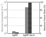
도 3은 AgNP 및 AgNP-Ga-In 사이의 전기 전도성 및 최대 스트레인의 차이를 도시하는 그래프이다.
도 4A 및 도 4B는 각자 EGaIn 처리 전 그리고 후의 전도성 잉크의 현미경 사진이다.
도 5A 및 도 5B는 도 4A 및 도 4B에 도시된 현미경 사진의 더 높은 확대율로 도시된 것으로서, 액체 금속이 어떻게 AgNP가 골재로 클러스터가 되게 야기하는지를 도시하는 현미경 사진이다.
도 6은 25μm 길이의 스캔 선(scanning line)으로 실행된 EDS 분석으로, Ag, Ga 및 In 농도 프로파일을 도시한다.
도 7은 폴리머 기판 상의 전도성 트레이스에 대한 스트레인 대 전기 저항성을 도시하는 그래프이다.
도 8은 수전사(hydrographic transfer)로 배치된 회로를 가진 3D 인쇄된 손 모형을 도시한다.
도 9는 사람 팔에 배치된, 전자 문신으로서 기능을 하는 회로를 도시한다.
도 10은 3D 인쇄된 물체에 전사된 회로를 도시한다.
도 11A 및 도 11B는 뇌 모형에 전사된 전도성 트레이스가 모형의 형태가 변형되었을 때에도 전도성을 유지하는 것을 도시한다. 1 shows a process for making a conductive trace according to one embodiment of the invention.
2A and 2B are micrographs of AgNP inks printed before and after lamination of EGaIn, respectively.
3 is a graph showing the difference in electrical conductivity and maximum strain between AgNP and AgNP-Ga-In.
4A and 4B are micrographs of the conductive ink before and after EGaIn treatment, respectively.
5A and 5B are shown at a higher magnification of the micrographs shown in FIGS . 4A and 4B and are micrographs showing how the liquid metal causes AgNP to cluster into aggregates.
FIG. 6 is an EDS analysis performed with a scan line of 25 μm length, showing the Ag, Ga and In concentration profiles.
7 is a graph depicting strain versus electrical resistance to conductive traces on a polymer substrate.
8 shows a 3D printed hand model with circuits arranged by hydrographic transfer.
9 shows a circuit that functions as an electronic tattoo, placed on the human arm.
10 shows a circuit transferred to a 3D printed object.
11A and 11B show that the conductive traces transferred to the brain model retain conductivity even when the shape of the model is deformed.
본원에 사용된 바와 같이 용어 "액체 금속"은 30℃ 이하의 온도에서 액상인 어느 금속 또는 금속 합금을 의미한다. 예로는 갈륨, 갈륨-인듐 합금, 및 갈륨-인듐-주석 합금이 있다.As used herein, the term "liquid metal" means any metal or metal alloy that is liquid at a temperature of 30 ° C or lower. Examples are gallium, gallium-indium alloy, and gallium-indium-tin alloy.
전도성 잉크 및 페이스트는 보통 마이크로입자 또는 나노입자를 함유하는 제제 또는 캐리어 매체로 만들어진다. 대부분의 그러한 잉크는 전도성이 아니거나 또는 배치 직후에 저조한 전도성을 갖는다. 그는 트레이스를 전도성으로 만들기 위해 가열 또는 빛을 기반으로 할 수 있는 소결 과정을 필요로 한다. 소결 과정 후, 이 잉크는 전도성이 되기는 하지만 신축성은 갖지 않는다. 인쇄된 회로에 가해지는 약한 스트레인으로도 트레이스에 금이 가서 더 이상 전도성이 아니게 만든다.Conductive inks and pastes are usually made of microparticles or nanoparticle-containing formulations or carrier media. Most such inks are not conductive or have poor conductivity immediately after placement. He needs a heating or light-based sintering process to make the trace conductive. After the sintering process, the ink becomes conductive but not stretchable. Even a weak strain on the printed circuit will crack the trace and make it no longer conductive.
본 발명의 한 구체예에서 인쇄된 트레이스 위로 액체 금속의 도포는 전도성을 10배로 향상시키기 때문에 열 또는 빛 기반(light-based) 소결의 필요성을 제거한다. 이 과정은 나노입자의 더 나은 응집 및 자가 조립을 돕고, 그렇게 함으로써 전도성 경로를 생성한다. 예를 들어서, 50MΩ 이상의 저항성을 갖는 인쇄된 트레이스는 이 과정의 적용 후 그의 저항성이 30Ω 이하로 감소되었다. 그에 더하여, 그 결과로 트레이스는 전도성을 잃지 않고도 큰 스트레인을 견딜 수 있다.In one embodiment of the present invention, the application of a liquid metal over a printed trace eliminates the need for thermal or light-based sintering because it improves conductivity by a factor of 10. This process helps better aggregation and self-assembly of the nanoparticles, thereby creating a conductive path. For example, printed traces with a resistivity of 50 MΩ or more were reduced to 30 Ω or less after application of this process. In addition, as a result, the traces can withstand large strains without losing conductivity.
다른 구체예에서, 유사한 결과를 제공하는 인쇄 가능한 물질은 공융 갈륨/인듐 합금을 은 또는 구리 입자와 사전에(인쇄 전에) 혼합(pre-mixing)하는 것으로 만들 수 있다. 다시 말해서 상기 잉크는 소결 과정을 필요로 하지 않는다. 그렇기 때문에 그의 적용은 내열성 기판에 제한되지 않는다. 또한 적층된 잉크는 전도성을 잃지 않고도 그의 초기 길이의 100%까지 늘일 수 있다. 전기 전도성 패턴을 만들기 위한 인쇄 가능한 물질은 캐리어 매체에 현탁된 금속 입자 및 상기 캐리어 매체에 혼합된 액체 금속을 포함할 수 있고, 이 혼합물은 액체 금속의 최소 0.1% 중량퍼센트이다. 여러 구체예에서 상기 금속 입자는 은 입자 또는 은 코팅된 입자, 구리 입자 또는 구리 코팅된 입자, 금 입자 또는 금 코팅된 입자 또는 니켈 입자 또는 니켈 코팅된 입자를 포함하는 군으로부터 선택된 금속의 크기 범위가 1nm에서 1mm에 이르는 구체, 비즈, 플레이크, 와이어, 또는 튜브를 포함할 수 있지만 이에 한정되지는 않는다. 상기 액체 금속은 바람직하게는 갈륨 및 인듐의 공융 합금이다. 여러 구체예에서 상기 캐리어 매체는 인쇄 가능한 물질의 점도를 조절하기 위해 희석될 수 있는 액체 또는 폴리머일 수 있다. 상기 액체 금속은 원심, 플래너터리(planetary), 및 수동 혼합 및 초음파 혼합을 포함하는 전단력 혼합을 포함하지만 이에 제한되지는 않은 어느 공지된 방법으로도 캐리어 매체 및 금속 입자에 혼합될 수 있다.In other embodiments, printable materials that provide similar results can be made by pre-mixing the eutectic gallium / indium alloy with silver or copper particles (before printing). In other words, the ink does not require a sintering process. As such, its application is not limited to heat-resistant substrates. In addition, the layered ink can be stretched to 100% of its initial length without losing conductivity. The printable material for making the electrically conductive pattern can include metal particles suspended in a carrier medium and liquid metal mixed in the carrier medium, the mixture being at least 0.1% by weight of the liquid metal. In various embodiments, the metal particles have a size range of a metal selected from the group comprising silver particles or silver coated particles, copper particles or copper coated particles, gold particles or gold coated particles or nickel particles or nickel coated particles. Spheres ranging from 1 nm to 1 mm, beads, flakes, wires, or tubes. The liquid metal is preferably a eutectic alloy of gallium and indium. In various embodiments, the carrier medium can be a liquid or polymer that can be diluted to control the viscosity of the printable material. The liquid metal can be mixed into the carrier medium and metal particles by any known method including, but not limited to, centrifugal, planetary, and shear force mixing including manual mixing and ultrasonic mixing.
한 구체예에서, 회로는 본원에 개시된 방법을 사용하여 타투 전사지, 전사지 또는 수전사 용지(hydrographic paper)에 인쇄될 수 있고 그리고 그 후에 거의 모든 3D 표면에 전사될 수 있다. 이는 바이오모니터링을 위해 회로를 인체에, 또는 플라스틱 부품, 벽, 테이블, 납땜한 전자 장치를 갖는 인쇄된 회로, 또는 3D 인쇄된 부품과 같은 어느 물체에도 전사될 수 있다. 이는 전자 장치와는 상관 없이 부품의 생성 후에 그 위로 전자 회로를 전사하는 것을 가능하게 한다. 다른 구체예에서는 상기 회로가 굽힘성(bendability)을 고려하여 폴리머 기판에도 인쇄될 수 있다. 또 다른 구체예에서는 상기 회로가 종이, 직물, 세라믹, 목재 또는 폼(foam)을 포함하지만 이에 제한되지는 않는 비폴리머 기판에 직접적으로 인쇄될 수 있다.In one embodiment, the circuit can be printed on a tattoo transfer paper, transfer paper or hydrographic paper using the methods disclosed herein and then transferred to almost all 3D surfaces. It can be transferred to the human body for biomonitoring, or to any object such as a plastic part, a wall, a table, a printed circuit with soldered electronics, or a 3D printed part. This makes it possible to transfer the electronic circuit over it after creation of the part, regardless of the electronic device. In other embodiments, the circuit may be printed on a polymer substrate in consideration of bendability. In another embodiment, the circuit can be printed directly on a non-polymer substrate including, but not limited to, paper, textile, ceramic, wood, or foam.
이 과정은 인몰드(in-mold) 전자 장치를 수반하는 적용, 즉 진공 성형을 거친 부품 위에 전자 장치를 전사하는 것 또는 오직 신축성 잉크로만 작업할 수 있는 유사한 과정에 있어서 특히 흥미롭다. 직물 전자 기술(textile electronics) 및 전송, 바이오모니터링 패치 및 박막 타투 같은 패치, 그리고 박막 배터리, 태양 전지판, 인쇄된 트랜지스터, OLED, 투명 전도성 필름, 초박형 압력 필름(ultrathin pressure films), 인간-기계 상호작용, 인터랙티브 아트, 인쇄된 디스플레이, 상호작용 패키징(interactive packaging) 등과 같은 여러가지 다른 영역에서의 적용 또한 있다.This process is particularly interesting for applications involving in-mold electronics, ie transferring the electronics over vacuum-formed parts, or similar processes that can only work with stretchable inks. Textile electronics and transmission, biomonitoring patches and patches such as thin-film tattoos, and thin-film batteries, solar panels, printed transistors, OLEDs, transparent conductive films, ultrathin pressure films, human-machine interaction There are also applications in several other areas, such as interactive art, printed displays, interactive packaging, and the like.
도 1에 도시된 바와 같이, 한 구체예에서 액체 금속 처리는 타투 스티커 용지에 인쇄된 은 기반의 전도성 잉크 회로의 전도성 및 기계적 변형능을 대폭 향상시킨다. 상기 회로는 AgNP 잉크를 타투 필름(tattoo film)에 인쇄하고, 그런 다음 인쇄된 잉크를 공융 갈륨-인듐(EGaIn)으로 코팅하는 것으로 만들어진다. EGaIn은 상온에서 액상이고 그리고 얇고, 고전도성이며 기계적으로 견고한 반고체의 회로 트레이스를 형성하기 위해 은과 혼합되는 무독성 금속 합금이다.As shown in FIG . 1 , in one embodiment, the liquid metal treatment greatly improves the conductivity and mechanical deformability of the silver-based conductive ink circuit printed on the tattoo sticker paper. The circuit is made by printing AgNP ink on a tattoo film and then coating the printed ink with eutectic gallium-indium (EGaIn). EGaIn is a non-toxic metal alloy that is liquid at room temperature and mixed with silver to form a thin, highly conductive, mechanically robust semi-solid circuit trace.
통상적인 소결과는 대조적으로, 은 나노입자는 Ga가 풍부한 필름에 둘러싸인 AgNP-In-Ga 클러스터로 구성된 이질(heterogeneous) 물질을 형성하기 위해 액체 합금과 상호작용한다. 이 트레이스는 80%까지의 축의 스트레인(axial strain)에 있어서 높은 전기 전도성 및 낮은 전기 기계 결합(게이지율 ~1)을 유지하고 그리고 완전한 전기 또는 기계적 고장 전에 100% 이상의 스트레인을 견딜 수 있다. 생성 과정이 대기 조건 및 불활성 화학 환경에서 실행되기 때문에, 회로는, 예를 들어, 폴리머 박막을 포함하는 넓은 범위의 기판에 인쇄될 수 있다. 이 기법은 미세제조(microfabrication), 박막 금속 적층, 및 석판 인쇄 패터닝의 필요성을 제거하는 것으로 제조 과정을 크게 간소화시킨다. 대신에 Ag 트레이스는 데스크톱 잉크젯 프린터로 인쇄되고, 그런 다음 간단한 적층 및 세척 기법을 사용하여 얇은 층의 EGaIn으로 코팅된다.In contrast to conventional sintering, silver nanoparticles interact with a liquid alloy to form a heterogeneous material composed of AgNP-In-Ga clusters surrounded by a Ga-rich film. This trace maintains high electrical conductivity and low electromechanical coupling (gauge ratio ~ 1) for axial strain up to 80% and can withstand strains of 100% or more before a complete electrical or mechanical failure. Since the production process is carried out in atmospheric conditions and inert chemical environments, the circuit can be printed on a wide range of substrates, including, for example, polymer thin films. This technique greatly simplifies the manufacturing process by eliminating the need for microfabrication, thin film metal lamination, and lithographic patterning. Instead, the Ag trace is printed with a desktop inkjet printer, and then coated with a thin layer of EGaIn using simple lamination and cleaning techniques.
도 1A에 도시된 바와 같이, 회로는 다음의 과정 단계로 만들어진다: 제일 먼저, 예를 들어 AgNP 잉크와 같은 전도성 잉크를 포함하는 하나 이상의 전기 트레이스로 이루어진 회로가 폴리머 필름에 적층된다(i). 전기 트레이스의 적층은 어느 방식으로도, 예를 들어 잉크젯 인쇄, 스크린 인쇄, 롤투롤(roll-to-roll) 인쇄, 에어로졸 적층, 밀착 인화 또는 스핀 코팅에 의한 균일 박막 적층, 또는 공지되었거나 또는 아직 개발되지 않은 어느 다른 방법으로도 완수될 수 있다. 회로의 초기 인쇄에는 전도성 잉크 또는 페이스트가 사용될 수 있다. 일부 구체예에서 그러한 잉크는 나노입자 또는 마이크로입자 형태의 은, 구리 또는 금, 크기 범위가 1nm에서 1mm에 이르는 플레이크, 와이어, 또는 튜브, 은, 구리 또는 금으로 코팅된 입자 또는 은, 구리 또는 금 염을 포함할 수 있다. 바람직한 구체예에서는 은의 나노입자(AgNP)를 포함하는 전도성 잉크가 사용된다. 본원의 설명을 위해서 AgNP가 사용되기는 하지만, 본 발명이 AgNP 기반의 전도성 잉크를 사용하는 것으로 제한되지 않는다는 것을 인식해야 한다.As shown in Fig . 1A , the circuit is made of the following process steps: First, a circuit consisting of one or more electrical traces comprising a conductive ink, for example AgNP ink, is deposited on the polymer film (i). Lamination of the electrical traces can be done in any way, for example inkjet printing, screen printing, roll-to-roll printing, aerosol lamination, uniform thin film lamination by adhesion printing or spin coating, or known or still in development It can be accomplished in any other way that has not been done. Conductive ink or paste may be used for initial printing of the circuit. In some embodiments such inks are silver, copper or gold in the form of nanoparticles or microparticles, flakes, wires or tubes ranging in size from 1 nm to 1 mm, particles coated with silver, copper or gold, or silver, copper or gold Salts. In a preferred embodiment, a conductive ink containing silver nanoparticles (AgNP) is used. Although AgNP is used for the purposes of the present description, it should be appreciated that the present invention is not limited to using AgNP based conductive inks.
그 다음에는 소량의 액체 공융 갈륨/인듐 합금(EGaIn)을 적층시키고(ii) 그리고 보푸라기가 없는 천을 사용하여 회로에 문질러 발라(iii) 회로 전체를 덮는다(iv). 대안적인 구체예에서는 다른 액체 금속을 사용하거나 또는 수동 표면 코팅, 스핀 코팅, 분무 적층, 딥 코팅, 롤투롤 코팅, 나이프 코팅 및 그라비어 코팅을 포함하지만 이에 제한되지는 않는 다른 액체 금속 도포 방법이 사용될 수 있다. 바람직하게는 액체 금속이 50℃ 이하의 온도일 것이다. 본 발명은 예시로 액체 매체를 사용하여 설명하지만, 필요한 성질을 갖는 어느 적합한 액체 금속이라도 사용될 수 있다. 그런 다음에 이전에 회로가 인쇄된 부분을 제외한 회로의 나머지 부분으로부터 액체 금속을 비젖게 하는(dewets) 약한 수용액 또는 염기성 용액, 또는 아세트산 또는 염산 증기(v)와 같은 증기를 적용시키는 것으로 초과로 남은 EGaIn이 제거된다. 완전히 세척된 후(vi), 상기 회로에는 표면 장착 칩이 장착될 수 있다(vii). 최종적인 회로는 그의 캐리어 필름으로부터 탈착되어(viii) 사람 피부와 같은 3D 표면에 전사될 준비가 된다.Next, a small amount of liquid eutectic gallium / indium alloy (EGaIn) is laminated (ii) and rubbed into the circuit using a lint-free cloth (iii) to cover the entire circuit (iv). Alternative liquid metals may be used in alternative embodiments or other liquid metal application methods, including but not limited to, manual surface coating, spin coating, spray lamination, dip coating, roll-to-roll coating, knife coating and gravure coating. have. Preferably the liquid metal will be at a temperature of 50 ° C or lower. The present invention is illustrated using a liquid medium as an example, but any suitable liquid metal having required properties can be used. Then the excess remained by applying a weak aqueous or basic solution, or acetic acid or hydrochloric acid vapor (v), which wets the liquid metal from the rest of the circuit, except for the portion where the circuit was previously printed. EGaIn is removed. After being completely cleaned (vi), the circuit may be equipped with a surface mount chip (vii). The final circuit is ready to be detached from its carrier film (viii) and transferred to a 3D surface such as human skin.
여러 구체예에서 액체 금속은 수동 닦기(manual wiping), 가스 압력 또는 유압, 초음파 세척, 산 증기, 산성 또는 염기성 액체 세척 및 전압 적용을 포함하지만 이에 제한되지는 않는 어느 공지된 방법을 사용하여 기판로부터 세척될 수 있다.In various embodiments the liquid metal is removed from the substrate using any known method including, but not limited to, manual wiping, gas pressure or hydraulic, ultrasonic cleaning, acid vapor, acidic or basic liquid cleaning and voltage application. Can be washed.
일부 구체예에서 액체 금속은 기판은 위는 피하면서 회로의 인쇄된 트레이스 위에 선택적으로 적층될 수 있고, 그러므로 세척 단계의 필요성을 제거한다. 선택적인 적층 방법은 스크린 인쇄, 전기도금, 잉크젯 인쇄 및 밀착 인화를 포함하지만 이에 제한되지는 않는, 물질을 선택적으로 적층하는 어느 공지된 방법이라도 될 수 있다.In some embodiments, the liquid metal can be selectively deposited over the printed traces of the circuit while avoiding the substrate, thus eliminating the need for a cleaning step. The optional lamination method can be any known method of selectively laminating materials, including, but not limited to, screen printing, electroplating, inkjet printing, and adhesion printing.
대안적인 구체예에서는 빈 공간이 없는 한 층의 금속 잉크가 먼저 기판 위에 전체적으로 인쇄되고, 액체 금속의 가득 채운 한 층의 적층이 뒤를 따르고, 그리고 회로의 패터닝을 위한 레이저 어블레이션이 뒤를 따른다.In an alternative embodiment, a layer of metallic ink without voids is first printed entirely over the substrate, followed by a stack of layers filled with liquid metal followed by laser ablation for patterning of the circuit.
도 2A에 도시된 바와 같이, EGaIn 적층 전에, AgNP 잉크는 저밀도의 AgNp 및 퍼콜레이션 부족 때문에 비전도성이다. 도 2B에 도시된 바와 같이, EGaIn이 첨가되었을 때, 그는 나노입자가 응집되게 하고 그리고 이어진 금속 필름을 형성하기 위해 틈을 채운다. 인쇄된 Ag-Ga-In 회로 내의 액상 합금의 존재는 회로의 신축성에 기여한다. 도 3에 도시된 바와 같이, EGaIn 적층은 인쇄된 회로에 있어서 3.6에서 4.85x10⁶S·m-1으로 용적 전도성의 여섯 크기 정도만큼의 증가 및 박막 회로의 최대 파괴 스트레인이 4.5%에서 118%로 25x 이상의 증가를 야기하는 것으로 관찰되었다. 또한 그러한 회로는 굉장히 유연하고 그리고 도 11에 도시된 것과 같은 뇌 모형 같이 곡선이고, 두드러진 질감 표현(highly textured)을 갖고, 전개 불가한 3D 표면에 전사될 수 있을만큼 충분한 스트레인을 지원할 수 있다.As shown in Figure 2A , prior to EGaIn deposition, AgNP inks are non-conductive due to low density of AgNp and lack of percolation. As shown in Figure 2B , when EGaIn is added, he causes the nanoparticles to agglomerate and fill the gaps to form a continuous metal film. The presence of the liquid alloy in the printed Ag-Ga-In circuit contributes to the stretchability of the circuit. As shown in Fig . 3 , the EGaIn stacking increased from 3.6 to 4.85x10 6 S · m -1 by six orders of magnitude in volumetric conductivity in printed circuits and the maximum breaking strain of thin film circuits from 4.5% to 118%. It was observed to cause an increase of 25x or more. Also, such circuits are extremely flexible and curved like a brain model as shown in FIG . 11 , have a highly textured, and can support sufficient strain to be transferred to an undevelopable 3D surface.
AgNP-Ga-In 혼합물의 특징 및 구성을 조사하기 위해 주사 전자 현미경(SEM) 및 에너지 분산형 X선 분광법(EDS)이 사용되었다. EGaIn 처리 전과 후의 전도성 잉크의 현미경 사진이 각자 도 4A 및 도 4B에 도시된다. 더 낮은 확대율에서는 전도성 트레이스 내의 많은 수의 작은 금을 명확하게 볼 수 있다. 이 금은 인쇄 후 용매 증발 및 결과로서 발생하는 은 잉크의 수축으로 인해 타투 필름에 형성된다. 그러나 도 4B에 도시된 바와 같이 대부분의 작은 금은 처리 후에 액체 금속으로 완전히 채워진다.Scanning electron microscopy (SEM) and energy dispersive X-ray spectroscopy (EDS) were used to investigate the characteristics and composition of the AgNP-Ga-In mixture. Micrographs of the conductive ink before and after EGaIn treatment are shown in FIGS. 4A and 4B , respectively. At lower magnifications, a large number of small golds in the conductive traces are clearly visible. This gold is formed on the tattoo film due to solvent evaporation after printing and shrinkage of the resulting silver ink. However , as shown in Figure 4B , most of the small gold is completely filled with liquid metal after treatment.
도 5A 및 도 5B에서 더 높은 확대율에서 관찰할 수 있는 바와 같이, 액체 금속은 AgNP가 개별 입자보다 적어도 5x 더 큰 골재로 클러스터되는 것 또한 야기한다. 이 골재는 향상된 전반적인 전도성에 기여할 수 있는 증가된 표면 조도를 갖는 연결된 덩어리를 형성한다. 도 6을 참조하면, 25μm 길이의 스캔 선(scanning line)으로 실행된 EDS 분석은 Ag 및 In 농도 프로파일은 서로 유사하지만 Ga 프로파일에 관해서는 반대라는 것을 보여준다. 특히 흰색 영역에서 많은 양의 Ag 및 In과 적은 양의 Ga가 발견되는데, 이는 AgNP-Ga-In 클러스터의 위치와 일치한다. 그에 반해서 클러스터 바깥의 회색 영역에서는 고농도의 Ga가 감지된다. 이미지 상에서 흰색 및 회색 영역 모두 인쇄된 AgNP-Ga-In 트레이스 내에 위치한다는 것에 주목해야 한다. EDS 분석은 Ga가 풍부한 영역 내에서 Ga:In 비율이 ~3:1(즉 원래의 EGaIn 합금의 것과 유사하다)인 반면, AgNP-Ga-In 클러스터에서는 약 1:2인 것을 입증한다.As can be observed at higher magnifications in Figures 5A and 5B , the liquid metal also causes AgNP to cluster into aggregates that are at least 5x larger than the individual particles. This aggregate forms a linked mass with increased surface roughness that can contribute to improved overall conductivity. Referring to FIG. 6 , EDS analysis performed with a scanning line of 25 μm length shows that Ag and In concentration profiles are similar to each other, but opposite to Ga profiles. In particular, a large amount of Ag and In and a small amount of Ga are found in the white region, which coincides with the location of the AgNP-Ga-In cluster. In contrast, a high concentration of Ga is detected in the gray region outside the cluster. It should be noted that both the white and gray areas on the image are located within the printed AgNP-Ga-In trace. EDS analysis demonstrates that the Ga: In ratio in the Ga-rich region is ˜3: 1 (ie similar to that of the original EGaIn alloy), while in the AgNP-Ga-In cluster it is about 1: 2.
큰 기계적 변형 하의 전도성 AgNP-Ga-In의 기능성은 박막 폴리머 기판에 인쇄된 전도성 트레이스를 널리 쓰이는 실리콘 기반의 유기 폴리머인 폴리디메틸실록산(PDMS)의 두 개의 층 사이에 넣고, 그리고 그를 표준 "도그 본(dogbone)" 모양으로 절단하는 것으로도 입증될 수 있다. 그런 다음에 사람 피부로 전자 문신을 전사하는 기계 부하 조건을 복제하기 위해 표본에 단축 인장 부하가 가해진다. 도 7에 도시된 바와 같이, 상기 표본은 80%까지 그리고 그 이상의 적용된 스트레인 하에서도 높은 전기 전도성을 유지하고 그리고 반복 가능하고 신뢰할 수 있는 전기 기계 반응을 보인다. 그러나 일부 경우에서는 표본의 실패 스트레인(failure strains)이 동일한 부하 조건 및 생성 과정에서 최대 118%까지 측정되었다. 인장 시험의 속도를 변경하거나 또는 상이한 너비의 전도성 트레이스를 사용하는 것은 전도성 AgNP-Ga-In 트레이스의 전기 기계 반응에 오직 작은 영향만을 미쳤다. 지속적인 기계적 주기 중에 계속 전기 전도성이고 그리고 적정한 전기 기계 결합을 유지하는 표본의 능력은 이 전자 문신이 인체에 일상적으로 사용되기에 충분한 내구성을 가질 수 있다는 것을 시사한다.The functionality of conductive AgNP-Ga-In under large mechanical strain is placed between two layers of polydimethylsiloxane (PDMS), a silicon-based organic polymer widely used for conductive traces printed on thin film polymer substrates, and the standard "dog bone" (dogbone) "can also be proven to cut. The specimen is then subjected to a uniaxial tensile load to replicate the mechanical loading conditions that transfer the electronic tattoo to the human skin. As shown in FIG . 7 , the specimen maintains high electrical conductivity up to 80% and under applied strain and exhibits repeatable and reliable electromechanical response. However, in some cases, the specimen's failure strains were measured up to 118% under the same loading conditions and production. Changing the speed of the tensile test or using conductive traces of different widths had only a small effect on the electromechanical reaction of the conductive AgNP-Ga-In traces. The ability of the specimen to remain electrically conductive and maintain proper electromechanical bonding during a sustained mechanical cycle suggests that this electronic tattoo can be durable enough for daily use in the human body.
상기 회로는 수전사를 사용하여 3D 물체에 배치될 수 있다. 회로가 배치된 3D 인쇄된 손 모형이 도 8에 도시된다. 도 9에 도시된 바와 같이 사람 팔에 배치되어 상기 회로가 비주얼 디스플레이 및 전력 조절을 위한 온보드(on-board) 마이크로 전자 칩을 가진 전자 문신으로서 기능하는 것 또한 가능하다. 도 10은 3D 인쇄된 물체 위에 배치된 회로를 도시한다. 또한 도 11A에 도시된 바와 같이, 초박형 전도성 트레이스의 신축성은 LED가 탑재된 질감 표현이 강한 뇌 모형에서도 입증된다. 도 11B에 도시된 바와 같이, 폼을 쥐어짜듯이 쥐는 것은 회로를 변형시키지만, LED의 작동에 지장을 주지 않아 기능이 유지된다. 이 회로는 신축성 AgNP-Ga-In 전도체의 기계적 견고함과 기능성을 입증하는 예시 중 극히 일부일 뿐이다.The circuit can be placed on a 3D object using a water transfer. A 3D printed hand model with circuit arrangement is shown in FIG . 8 . It is also possible for the circuit to function as an electronic tattoo with an on-board microelectronic chip for visual display and power control as placed in the human arm as shown in FIG . 9 . 10 shows a circuit disposed on a 3D printed object. In addition, as shown in FIG . 11A , the elasticity of the ultra-thin conductive trace is also demonstrated in a brain model having a strong texture expression with LEDs. As shown in Fig . 11B , squeezing the foam as it squeezes the circuit, but does not interfere with the operation of the LED, so that its function is maintained. This circuit is only a small subset of examples demonstrating the mechanical robustness and functionality of the stretchable AgNP-Ga-In conductor.
본원에는 연성이며 신축성이 있는 박막 전기 장치를 빠르게 만드는 기법이 개시된다. 회로는 기계적으로 견고한 전도성 트레이스를 형성하기 위해 상온에서 공융 갈륨-인듐 합금(EGaIn)과 상호작용하는, 잉크젯으로 인쇄되는 은 나노입자로 생성된다. EGaIn 코팅을 사용하여, 상기 트레이스는 전기 전도성에서 x106 증가를 보이고 그리고 80% 스트레인까지 구부러지거나 늘어났을 때 낮은 트레이스 저항을 유지한다. PDMS와 같은 연성 엘라스토머 기판에서 상기 트레이스는 수백 회의 부하 주기 동안 변함없는 적정한 전기 기계 반응(예를 들어 50% 스트레인에서 전기 저항의 50% 증가; 게이지율 ~1)을 보인다.Disclosed herein are techniques for rapidly making flexible, stretchable thin film electrical devices. The circuit is created with inkjet printed silver nanoparticles that interact with a eutectic gallium-indium alloy (EGaIn) at room temperature to form a mechanically robust conductive trace. Using an EGaIn coating, the trace shows an x10 6 increase in electrical conductivity and maintains low trace resistance when bent or stretched to 80% strain. On flexible elastomeric substrates such as PDMS, the traces exhibit a constant and consistent electromechanical response (eg, 50% increase in electrical resistance at 50% strain; gauge rate ~ 1) over hundreds of load cycles.
타투 스티커 용지에 인쇄되었을 때, 상기 회로는 수전사를 사용하여 3D 표면에 배치되거나 또는 전자 문신으로서 피부에 할 수 있다. 상기 회로는 늘어날 수 있기 때문에 고도로 굽어 있거나 또는 전개 불가한(예를 들어 구체의) 표면에 전사되거나 또는 상당한 스트레인을 겪는 신체의 일부분에 배치될 수 있다. 또한 신축성 전자 장치(예를 들어 전도성 엘라스토머, 물결모양(wavy) 회로, EGaIn 미세유체학 등)에 대한 다른 접근법과는 달리, 박막 회로는 통상의 잉크젯 프린터를 사용하여 생성될 수 있다. 이 새로운 방법은 이전에 볼 수 없었던 연성 피부 부착(on-skin) 전자 장치의 사용자 조정 자유도가 높고(highly customized) 그리고 실현 가능한 생성 기법으로 이어진다. 앞으로의 노력은 다양한 기판에 인쇄된 AgNP-Ga-In 회로의 더 나아간 원소 및 지형의 특성화, 최대 신축성 및 전도성을 달성하기 위한 AgNP 인쇄, 적층, 및 세척 기법의 최적화, 전사 기법의 최적화, 그리고 바이오모니터링을 위해 신체에 부착되고 그리고 상호적인 HMI를 위해 3D 표면 위에 배치되는 일련의 박막 전자 피부(e-skin)의 시범에 집중할 것이다.When printed on a tattoo sticker paper, the circuit can be placed on a 3D surface using a water transfer or applied to the skin as an electronic tattoo. Since the circuit can be stretched, it can be stretched onto a highly curved or unexpandable (eg, spherical) surface or placed on a part of the body that undergoes significant strain. Also, unlike other approaches to stretchable electronic devices (eg conductive elastomers, wavy circuits, EGaIn microfluidics, etc.), thin film circuits can be created using conventional inkjet printers. This new method leads to a highly customized and feasible creation technique for user-adjustable soft-on-skin electronic devices that has never been seen before. Future efforts include characterization of further elements and topography of AgNP-Ga-In circuits printed on various substrates, optimization of AgNP printing, lamination, and cleaning techniques to achieve maximum stretch and conductivity, optimization of transfer techniques, and bio We will focus on the demonstration of a series of thin-film electronic skins that are attached to the body for monitoring and placed on a 3D surface for interactive HMI.
본 발명의 범위는 본 발명을 설명하기 위해 본원에 제공된 어느 예시에 제한되는 것으로 여겨져서는 안 되고, 하기의 청구항의 범위로 정의되는 것이다.The scope of the present invention should not be considered limited to any examples provided herein to illustrate the present invention, but is defined by the scope of the following claims.
Claims (20)
하나 이상의 전기 트레이스를 액체 금속으로 코팅하는 단계를 포함하고,
상기 액체 금속이 갈륨; 갈륨 및 인듐의 합금; 또는 갈륨, 인듐 및 주석의 합금인 것을 특징으로 하는 전도성 전기 트레이스를 생성하는 방법.
Printing an electrical circuit comprising one or more traces on a substrate using conductive ink; And
Coating one or more electrical traces with a liquid metal,
The liquid metal is gallium; Alloys of gallium and indium; Or an alloy of gallium, indium and tin.
The method of claim 1, wherein the liquid metal is selectively deposited over a printed trace of the electrical circuit.
3. The method of claim 2, wherein the selective lamination is selected from the group comprising screen printing, electroplating, inkjet printing, and adhesion printing.
The method of claim 1, further comprising coating the substrate with a liquid metal and removing the liquid metal from the substrate, leaving the liquid metal on one or more traces.
5. Conductive electricity according to claim 4, wherein the liquid metal removal method is selected from the group comprising manual wiping, gas pressure or hydraulic pressure, ultrasonic cleaning, acid vapor, acidic or basic liquid cleaning and voltage application. How to create a trace.
According to claim 1, wherein the conductive ink is silver, copper or gold particles; Particles covered with silver, copper or gold; Or a liquid or paste containing a salt of silver, copper or gold.
The method of claim 1, wherein the liquid metal is a eutectic alloy of gallium and indium.
The method of claim 1, wherein the printing of the electrical traces is performed using a method selected from inkjet printing, screen printing, roll-to-roll printing, aerosol lamination, adhesion printing and uniform thin film lamination by spin coating. A method of generating a conductive electrical trace, characterized in that.
The conductive electricity of claim 1, wherein coating the one or more traces with a liquid metal enables percolation of the stacked metal particles to enable electrical conductivity or to increase electrical conductivity. How to create a trace.
The method of claim 1, wherein coating the one or more traces with a liquid metal increases resistance to mechanical strain or mechanical strain of the electrical circuit.
The method of claim 1, wherein the substrate is a polymer substrate.
The method of claim 1, wherein the substrate is a tattoo transfer paper, a transfer paper, or a hydrographic paper.
The method of claim 1, wherein the substrate is paper, textile, ceramic, wood, or foam.
The conductive electrical trace of claim 1, wherein the process for laminating the liquid metal is selected from the group consisting of manual surface coating, spin coating, spray lamination, dip coating, roll-to-roll coating, knife coating and gravure coating. How to generate.
패터닝 방법으로 상기 전기 회로의 형태를 정의하는 것을 더 포함하는 것을 특징으로 하는 전도성 전기 트레이스를 생성하는 방법.
The method of claim 1, wherein the substrate is covered with a full layer of conductive ink without voids, followed by a layer of liquid metal without voids, and
A method of generating a conductive electrical trace, further comprising defining a shape of the electrical circuit by a patterning method.
16. The method of claim 15, wherein the patterning method is selected from the group consisting of laser ablation and photolithography.
상기 캐리어 매체에 혼합된 액체 금속을 포함하는 혼합물로서,
상기 액체 금속이 갈륨 및 인듐의 합금이고,
상기 혼합물이 상기 액체 금속의 최소 0.1 중량%인 것을 특징으로 하는 전기 전도성 패턴을 생성하기 위한 인쇄 가능한 물질.
Metal particles suspended in a carrier medium; And
A mixture comprising a liquid metal mixed in the carrier medium,
The liquid metal is an alloy of gallium and indium,
Printable material for creating an electrically conductive pattern, characterized in that the mixture is at least 0.1% by weight of the liquid metal.
The method of claim 17, wherein the metal particles are silver particles or particles coated with silver; Copper particles or particles coated with copper; Spheres, beads, flakes, wires, or tubes ranging in size from 1 nm to 1 mm in metal size selected from the group containing gold particles or gold coated particles. Printable material characterized in that it comprises.
18. The printable material of claim 17, wherein the carrier medium is a liquid or polymer that can be diluted to control the viscosity of the printable material.
Applications Claiming Priority (7)
| Application Number | Priority Date | Filing Date | Title |
|---|---|---|---|
| US201762606187P | 2017-09-13 | 2017-09-13 | |
| US62/606,187 | 2017-09-13 | ||
| US201862762975P | 2018-05-25 | 2018-05-25 | |
| US62/762,975 | 2018-05-25 | ||
| PT20181000058782 | 2018-09-07 | ||
| PT15878218 | 2018-09-07 | ||
| PCT/US2018/050920 WO2019055680A1 (en) | 2017-09-13 | 2018-09-13 | Liquid metal fusion with conductive inks and pastes |
Publications (1)
| Publication Number | Publication Date |
|---|---|
| KR20200055009A true KR20200055009A (en) | 2020-05-20 |
Family
ID=70919326
Family Applications (1)
| Application Number | Title | Priority Date | Filing Date |
|---|---|---|---|
| KR1020207010052A KR20200055009A (en) | 2017-09-13 | 2018-09-13 | Liquid metal melt containing conductive ink and paste |
Country Status (4)
| Country | Link |
|---|---|
| US (2) | US11395413B2 (en) |
| EP (1) | EP3682717A4 (en) |
| KR (1) | KR20200055009A (en) |
| WO (1) | WO2019055680A1 (en) |
Cited By (2)
| Publication number | Priority date | Publication date | Assignee | Title |
|---|---|---|---|---|
| KR20230077363A (en) * | 2021-11-25 | 2023-06-01 | 한국화학연구원 | Positive photosensitive paste composition, electrode provided with conductive pattern using the same, and manufacturing method thereof |
| KR20240047508A (en) | 2022-10-04 | 2024-04-12 | 광주과학기술원 | Conductive water ink comprising liquid metal nanoparticle-conjugated polymer complex for and preparation method thereof |
Families Citing this family (18)
| Publication number | Priority date | Publication date | Assignee | Title |
|---|---|---|---|---|
| FR3067275B1 (en) | 2017-06-07 | 2022-08-12 | Timothee Boitouzet | PROCESS FOR PARTIAL DELIGNIFICATION BY SUPERCRITICAL OR SUBCRITICAL ROUTE AND FILLING OF A LIGNO-CELLULOSIC MATERIAL |
| KR102612806B1 (en) * | 2018-05-08 | 2023-12-11 | 더블유.엘. 고어 앤드 어소시에이트스, 인코포레이티드 | Flexible printed circuits for skin attachment |
| DE102018214367A1 (en) * | 2018-08-24 | 2020-02-27 | Karlsruher Institut für Technologie | Process for producing an electrically conductive connection on a substrate, microelectronic component and process for producing it |
| CN111849250A (en) * | 2019-04-30 | 2020-10-30 | 北京梦之墨科技有限公司 | Conductive ink and electronic device |
| US11706874B2 (en) * | 2019-08-06 | 2023-07-18 | Microsoft Technology Licensing, Llc | Electronic-circuit printing using low-cost ink |
| CN110828029A (en) * | 2019-11-06 | 2020-02-21 | 浙江清华柔性电子技术研究院 | Conductive material and preparation method thereof |
| WO2021146643A2 (en) * | 2020-01-15 | 2021-07-22 | Liquid Wire Inc. | Deposition with solid feedstock |
| KR102290112B1 (en) * | 2020-03-18 | 2021-08-13 | 포항공과대학교 산학협력단 | Conductive liquid metal microparticle comprising hydrogen-doped liquid metal oxide, conductive ink comprising same and method of fabricating same |
| US11937372B2 (en) | 2020-06-24 | 2024-03-19 | Yale University | Biphasic material and stretchable circuit board |
| FR3112449B1 (en) | 2020-07-08 | 2022-08-26 | Sas Woodoo | Method for manufacturing an electrically conductive device in lignocellulosic material |
| CN114496447B (en) * | 2020-10-26 | 2023-05-05 | 北京梦之墨科技有限公司 | Flexible radio frequency coil and preparation method thereof |
| US11631565B2 (en) | 2020-11-10 | 2023-04-18 | Science Applications International Corporation | Thermal fuse |
| CN114574039B (en) * | 2020-11-30 | 2023-02-10 | 北京梦之墨科技有限公司 | Cylindrical ink and printing ink tube |
| US20220306887A1 (en) * | 2021-03-24 | 2022-09-29 | Science Applications International Corporation | Self-Sintering Conductive Inks |
| CN113613395B (en) * | 2021-08-11 | 2022-12-27 | 东南大学 | Simple, convenient and efficient customized liquid metal circuit pattern printing method |
| CN113709996B (en) * | 2021-09-09 | 2023-10-31 | 北京星宇同辉科技有限公司 | High-conductivity electronic circuit capable of being printed rapidly at low temperature and preparation method and application thereof |
| CN115181453A (en) * | 2022-06-24 | 2022-10-14 | 温州大学新材料与产业技术研究院 | Gallium-containing metal conductive ink and preparation method and application thereof |
| CN115044081B (en) * | 2022-07-13 | 2023-10-24 | 清远高新华园科技协同创新研究院有限公司 | Liquid metal flexible film material and preparation method and application thereof |
Family Cites Families (9)
| Publication number | Priority date | Publication date | Assignee | Title |
|---|---|---|---|---|
| US20130202909A1 (en) * | 2012-02-06 | 2013-08-08 | Lg Chem, Ltd. | Method of producing metal nanoparticles |
| US10032538B2 (en) | 2013-11-13 | 2018-07-24 | The United States Of America As Represented By The Secretary Of The Army | Deformable elastomeric conductors and differential electronic signal transmission |
| US9841327B2 (en) * | 2014-08-14 | 2017-12-12 | Purdue Research Foundation | Method of producing conductive patterns of nanoparticles and devices made thereof |
| US10057981B2 (en) * | 2015-06-10 | 2018-08-21 | Industry Foundation Of Chonnam National University | Stretchable circuit board and method of manufacturing the same |
| EP3368145A1 (en) | 2015-10-30 | 2018-09-05 | Ecole Polytechnique Federale de Lausanne (EPFL) | Method for manufacturing electrical conductors, and electrical conductors manufactured according to same |
| US20170164461A1 (en) * | 2015-12-08 | 2017-06-08 | Intel Corporation | Conductive flexible and stretchable encapsulation method and apparatus |
| EP3424053B1 (en) | 2016-02-29 | 2021-09-15 | Liquid Wire Inc. | Liquid wire |
| US11220613B2 (en) * | 2017-04-18 | 2022-01-11 | Nanyang Technological University | Elastic conductor, device including, and method of forming the same |
| WO2019070872A1 (en) * | 2017-10-03 | 2019-04-11 | Northwestern University | Conductive graphene interfacial barriers for liquid metal electronics |
-
2018
- 2018-09-13 US US16/647,083 patent/US11395413B2/en active Active
- 2018-09-13 WO PCT/US2018/050920 patent/WO2019055680A1/en unknown
- 2018-09-13 EP EP18855315.0A patent/EP3682717A4/en active Pending
- 2018-09-13 KR KR1020207010052A patent/KR20200055009A/en active IP Right Grant
-
2022
- 2022-07-05 US US17/857,356 patent/US20220346238A1/en active Pending
Cited By (2)
| Publication number | Priority date | Publication date | Assignee | Title |
|---|---|---|---|---|
| KR20230077363A (en) * | 2021-11-25 | 2023-06-01 | 한국화학연구원 | Positive photosensitive paste composition, electrode provided with conductive pattern using the same, and manufacturing method thereof |
| KR20240047508A (en) | 2022-10-04 | 2024-04-12 | 광주과학기술원 | Conductive water ink comprising liquid metal nanoparticle-conjugated polymer complex for and preparation method thereof |
Also Published As
| Publication number | Publication date |
|---|---|
| EP3682717A4 (en) | 2021-06-23 |
| US20220346238A1 (en) | 2022-10-27 |
| EP3682717A1 (en) | 2020-07-22 |
| US20200221580A1 (en) | 2020-07-09 |
| US11395413B2 (en) | 2022-07-19 |
| WO2019055680A1 (en) | 2019-03-21 |
Similar Documents
| Publication | Publication Date | Title |
|---|---|---|
| KR20200055009A (en) | Liquid metal melt containing conductive ink and paste | |
| Lopes et al. | Hydroprinted electronics: ultrathin stretchable Ag–In–Ga E-skin for bioelectronics and human–machine interaction | |
| Agarwala et al. | Wearable bandage-based strain sensor for home healthcare: Combining 3D aerosol jet printing and laser sintering | |
| Huang et al. | Inkjet printing of silver nanowires for stretchable heaters | |
| Lopes et al. | Bi-phasic Ag–In–Ga-embedded elastomer inks for digitally printed, ultra-stretchable, multi-layer electronics | |
| TWI682405B (en) | Conductive silver paste | |
| Wang et al. | Advances in the development of liquid metal-based printed electronic inks | |
| Wu et al. | Buckle-delamination-enabled stretchable silver nanowire conductors | |
| Al-Milaji et al. | Direct embedment and alignment of silver nanowires by inkjet printing for stretchable conductors | |
| Ko et al. | Stretchable conductive adhesives with superior electrical stability as printable interconnects in washable textile electronics | |
| Huang et al. | Patterning of metal nanowire networks: methods and applications | |
| Zhu et al. | Fully solution processed liquid metal features as highly conductive and ultrastretchable conductors | |
| Cronin et al. | Photonic curing of low-cost aqueous silver flake inks for printed conductors with increased yield | |
| JP6690528B2 (en) | Conductive film | |
| TWI648751B (en) | Transparent conductive coatings on an elastomeric substrate | |
| Lee et al. | The development and investigation of highly stretchable conductive inks for 3-dimensional printed in-mold electronics | |
| Li et al. | Supermetallophobic functional coatings based on silicate clays and a method to pattern liquid metals | |
| Xiao et al. | Scalable strategy to directly prepare 2D and 3D liquid metal circuits based on laser-induced selective metallization | |
| Kim et al. | Simple, fast, and scalable reverse-offset printing of micropatterned copper nanowire electrodes with sub-10 μm resolution | |
| Yang et al. | Fabrication of flexible microheater with tunable heating capabilities by direct laser writing and selective electrodeposition | |
| WO2020161077A1 (en) | Method of manufacturing an elastic conductor, elastic conductor and electronic device comprising the elastic conductor | |
| Rahman et al. | Direct writing of stretchable metal flake conductors: improved stretchability and conductivity by combining differently sintered materials | |
| Šakalys et al. | Fabrication of multi-material electronic components applying non-contact printing technologies: A review | |
| Tan et al. | Fabrication Approaches of Soft Electronics | |
| Ji et al. | Laser patterning of highly conductive flexible circuits |
Legal Events
| Date | Code | Title | Description |
|---|---|---|---|
| A201 | Request for examination | ||
| E902 | Notification of reason for refusal | ||
| E902 | Notification of reason for refusal | ||
| E701 | Decision to grant or registration of patent right |