KR20200038034A - An electronic device including an antenna module - Google Patents
An electronic device including an antenna module Download PDFInfo
- Publication number
- KR20200038034A KR20200038034A KR1020180117623A KR20180117623A KR20200038034A KR 20200038034 A KR20200038034 A KR 20200038034A KR 1020180117623 A KR1020180117623 A KR 1020180117623A KR 20180117623 A KR20180117623 A KR 20180117623A KR 20200038034 A KR20200038034 A KR 20200038034A
- Authority
- KR
- South Korea
- Prior art keywords
- electronic device
- antenna module
- side member
- cover
- antenna
- Prior art date
Links
- 239000007769 metal material Substances 0.000 claims abstract description 23
- 229910052751 metal Inorganic materials 0.000 claims abstract description 12
- 239000002184 metal Substances 0.000 claims abstract description 12
- 238000004891 communication Methods 0.000 claims description 93
- 230000005855 radiation Effects 0.000 claims description 48
- 238000000034 method Methods 0.000 claims description 25
- 229910052755 nonmetal Inorganic materials 0.000 claims description 10
- 239000012811 non-conductive material Substances 0.000 claims description 4
- 230000000694 effects Effects 0.000 abstract description 2
- 239000000758 substrate Substances 0.000 description 24
- 239000010410 layer Substances 0.000 description 21
- 239000000463 material Substances 0.000 description 11
- 230000006870 function Effects 0.000 description 10
- 230000005540 biological transmission Effects 0.000 description 7
- 238000010586 diagram Methods 0.000 description 6
- 229920000642 polymer Polymers 0.000 description 6
- 230000008569 process Effects 0.000 description 5
- 238000004590 computer program Methods 0.000 description 4
- 239000000919 ceramic Substances 0.000 description 3
- 230000008961 swelling Effects 0.000 description 3
- 230000001133 acceleration Effects 0.000 description 2
- 229910052782 aluminium Inorganic materials 0.000 description 2
- XAGFODPZIPBFFR-UHFFFAOYSA-N aluminium Chemical compound [Al] XAGFODPZIPBFFR-UHFFFAOYSA-N 0.000 description 2
- 230000007613 environmental effect Effects 0.000 description 2
- 239000000446 fuel Substances 0.000 description 2
- 239000011521 glass Substances 0.000 description 2
- 238000012986 modification Methods 0.000 description 2
- 230000004048 modification Effects 0.000 description 2
- 230000002093 peripheral effect Effects 0.000 description 2
- 229920000515 polycarbonate Polymers 0.000 description 2
- 239000004417 polycarbonate Substances 0.000 description 2
- 239000002861 polymer material Substances 0.000 description 2
- 230000004044 response Effects 0.000 description 2
- 229910000679 solder Inorganic materials 0.000 description 2
- 230000005236 sound signal Effects 0.000 description 2
- 229910001220 stainless steel Inorganic materials 0.000 description 2
- 239000010935 stainless steel Substances 0.000 description 2
- 229910052724 xenon Inorganic materials 0.000 description 2
- FHNFHKCVQCLJFQ-UHFFFAOYSA-N xenon atom Chemical compound [Xe] FHNFHKCVQCLJFQ-UHFFFAOYSA-N 0.000 description 2
- FYYHWMGAXLPEAU-UHFFFAOYSA-N Magnesium Chemical compound [Mg] FYYHWMGAXLPEAU-UHFFFAOYSA-N 0.000 description 1
- 238000003491 array Methods 0.000 description 1
- 230000000903 blocking effect Effects 0.000 description 1
- 230000010267 cellular communication Effects 0.000 description 1
- 230000001413 cellular effect Effects 0.000 description 1
- 238000006243 chemical reaction Methods 0.000 description 1
- 239000003795 chemical substances by application Substances 0.000 description 1
- 239000011247 coating layer Substances 0.000 description 1
- 239000004020 conductor Substances 0.000 description 1
- 238000001816 cooling Methods 0.000 description 1
- 238000005516 engineering process Methods 0.000 description 1
- 230000010354 integration Effects 0.000 description 1
- 230000007774 longterm Effects 0.000 description 1
- 229910052749 magnesium Inorganic materials 0.000 description 1
- 239000011777 magnesium Substances 0.000 description 1
- 238000003825 pressing Methods 0.000 description 1
- 230000035807 sensation Effects 0.000 description 1
- 230000000638 stimulation Effects 0.000 description 1
Images


Classifications
-
- H—ELECTRICITY
- H01—ELECTRIC ELEMENTS
- H01Q—ANTENNAS, i.e. RADIO AERIALS
- H01Q1/00—Details of, or arrangements associated with, antennas
- H01Q1/12—Supports; Mounting means
- H01Q1/22—Supports; Mounting means by structural association with other equipment or articles
- H01Q1/24—Supports; Mounting means by structural association with other equipment or articles with receiving set
- H01Q1/241—Supports; Mounting means by structural association with other equipment or articles with receiving set used in mobile communications, e.g. GSM
- H01Q1/242—Supports; Mounting means by structural association with other equipment or articles with receiving set used in mobile communications, e.g. GSM specially adapted for hand-held use
- H01Q1/243—Supports; Mounting means by structural association with other equipment or articles with receiving set used in mobile communications, e.g. GSM specially adapted for hand-held use with built-in antennas
-
- H—ELECTRICITY
- H01—ELECTRIC ELEMENTS
- H01Q—ANTENNAS, i.e. RADIO AERIALS
- H01Q1/00—Details of, or arrangements associated with, antennas
- H01Q1/12—Supports; Mounting means
-
- H—ELECTRICITY
- H04—ELECTRIC COMMUNICATION TECHNIQUE
- H04M—TELEPHONIC COMMUNICATION
- H04M1/00—Substation equipment, e.g. for use by subscribers
- H04M1/02—Constructional features of telephone sets
- H04M1/0202—Portable telephone sets, e.g. cordless phones, mobile phones or bar type handsets
- H04M1/0249—Details of the mechanical connection between the housing parts or relating to the method of assembly
-
- H—ELECTRICITY
- H01—ELECTRIC ELEMENTS
- H01Q—ANTENNAS, i.e. RADIO AERIALS
- H01Q1/00—Details of, or arrangements associated with, antennas
- H01Q1/12—Supports; Mounting means
- H01Q1/22—Supports; Mounting means by structural association with other equipment or articles
-
- H—ELECTRICITY
- H01—ELECTRIC ELEMENTS
- H01Q—ANTENNAS, i.e. RADIO AERIALS
- H01Q1/00—Details of, or arrangements associated with, antennas
- H01Q1/36—Structural form of radiating elements, e.g. cone, spiral, umbrella; Particular materials used therewith
- H01Q1/38—Structural form of radiating elements, e.g. cone, spiral, umbrella; Particular materials used therewith formed by a conductive layer on an insulating support
-
- H—ELECTRICITY
- H01—ELECTRIC ELEMENTS
- H01Q—ANTENNAS, i.e. RADIO AERIALS
- H01Q1/00—Details of, or arrangements associated with, antennas
- H01Q1/52—Means for reducing coupling between antennas; Means for reducing coupling between an antenna and another structure
-
- H—ELECTRICITY
- H01—ELECTRIC ELEMENTS
- H01Q—ANTENNAS, i.e. RADIO AERIALS
- H01Q23/00—Antennas with active circuits or circuit elements integrated within them or attached to them
-
- H—ELECTRICITY
- H01—ELECTRIC ELEMENTS
- H01Q—ANTENNAS, i.e. RADIO AERIALS
- H01Q9/00—Electrically-short antennas having dimensions not more than twice the operating wavelength and consisting of conductive active radiating elements
- H01Q9/04—Resonant antennas
- H01Q9/16—Resonant antennas with feed intermediate between the extremities of the antenna, e.g. centre-fed dipole
-
- H—ELECTRICITY
- H04—ELECTRIC COMMUNICATION TECHNIQUE
- H04B—TRANSMISSION
- H04B1/00—Details of transmission systems, not covered by a single one of groups H04B3/00 - H04B13/00; Details of transmission systems not characterised by the medium used for transmission
- H04B1/38—Transceivers, i.e. devices in which transmitter and receiver form a structural unit and in which at least one part is used for functions of transmitting and receiving
- H04B1/40—Circuits
-
- H—ELECTRICITY
- H04—ELECTRIC COMMUNICATION TECHNIQUE
- H04M—TELEPHONIC COMMUNICATION
- H04M1/00—Substation equipment, e.g. for use by subscribers
- H04M1/02—Constructional features of telephone sets
- H04M1/0202—Portable telephone sets, e.g. cordless phones, mobile phones or bar type handsets
- H04M1/026—Details of the structure or mounting of specific components
- H04M1/0266—Details of the structure or mounting of specific components for a display module assembly
-
- H—ELECTRICITY
- H04—ELECTRIC COMMUNICATION TECHNIQUE
- H04M—TELEPHONIC COMMUNICATION
- H04M1/00—Substation equipment, e.g. for use by subscribers
- H04M1/02—Constructional features of telephone sets
- H04M1/0202—Portable telephone sets, e.g. cordless phones, mobile phones or bar type handsets
- H04M1/026—Details of the structure or mounting of specific components
- H04M1/0277—Details of the structure or mounting of specific components for a printed circuit board assembly
-
- H—ELECTRICITY
- H01—ELECTRIC ELEMENTS
- H01Q—ANTENNAS, i.e. RADIO AERIALS
- H01Q21/00—Antenna arrays or systems
- H01Q21/06—Arrays of individually energised antenna units similarly polarised and spaced apart
- H01Q21/061—Two dimensional planar arrays
- H01Q21/062—Two dimensional planar arrays using dipole aerials
-
- H—ELECTRICITY
- H01—ELECTRIC ELEMENTS
- H01Q—ANTENNAS, i.e. RADIO AERIALS
- H01Q21/00—Antenna arrays or systems
- H01Q21/06—Arrays of individually energised antenna units similarly polarised and spaced apart
- H01Q21/061—Two dimensional planar arrays
- H01Q21/065—Patch antenna array
-
- H—ELECTRICITY
- H01—ELECTRIC ELEMENTS
- H01Q—ANTENNAS, i.e. RADIO AERIALS
- H01Q21/00—Antenna arrays or systems
- H01Q21/29—Combinations of different interacting antenna units for giving a desired directional characteristic
Landscapes
- Engineering & Computer Science (AREA)
- Signal Processing (AREA)
- Computer Networks & Wireless Communication (AREA)
- Telephone Set Structure (AREA)
- Details Of Aerials (AREA)
Abstract
Description
본 문서에서 개시되는 실시 예들은 안테나 모듈을 포함하는 전자 장치와 관련된다.Embodiments disclosed in this document relate to an electronic device including an antenna module.
안테나는 상대적으로 낮은 주파수(3GHz 이하)로 작동하므로 전자 장치의 하우징을 이루는 메탈 소재를 방사체로 활용했다. 그러나, 이러한 방식은 직진성이 강한 높은 주파수(6GHz 이상)으로 작동하는 안테나에는 적용할 수 없다. 상대적으로 높은 주파수로 작동하는 안테나는 별도의 모듈로서 전자 장치 내부에 실장될 수 있다.Since the antenna operates at a relatively low frequency (below 3 GHz), a metal material constituting the housing of the electronic device is used as a radiator. However, this method cannot be applied to an antenna operating at a high frequency (6 GHz or higher) with strong linearity. The antenna operating at a relatively high frequency may be mounted inside the electronic device as a separate module.
이러한 안테나 모듈은 전파를 방사함에 있어서, 전자 장치의 외관을 형성하는 하우징의 소재에 의해 영향 받을 수 있다. 특히 최근의 모바일 전자 장치들은 하우징의 일부에 메탈 소재가 적용된다. In radiating radio waves, such an antenna module may be influenced by a material of a housing forming an external appearance of an electronic device. Particularly, in recent mobile electronic devices, a metal material is applied to a part of the housing.
메탈 소재의 하우징을 포함하는 전자 장치의 경우, 안테나 모듈로부터 방사되는 RF 신호가 하우징의 메탈 성분에 의해 영향 받을 수 있다. 본발명의 다양한 실시예에서는, 이를 해결하기 위한 안테나 모듈 배치 구조를 포함하는 전자 장치를 제공하고자 한다. In the case of an electronic device including a metal housing, the RF signal emitted from the antenna module may be affected by the metal component of the housing. In various embodiments of the present invention, an electronic device including an antenna module arrangement structure for solving this problem is provided.
다양한 실시 예에서, 전자 장치는 제1 방향으로 향하는 전면 플레이트, 상기 제1 방향의 반대 방향인 제2 방향으로 향하는 후면 플레이트, 및 상기 전면 플레이트와 상기 후면 플레이트 사이의 공간을 둘러싸고, 적어도 일부분이 금속 물질로 형성된 측면 부재를 포함하는 하우징; 상기 전면 플레이트를 통해 보여지는 디스플레이; 및 상기 공간 내에 위치하는 안테나 모듈로서, 상기 제1 방향 및 상기 제2 방향과는 다른 제3 방향으로 향하는 제1 면, 상기 제3 방향과 반대인 제4 방향으로 향하는 제2 면, 및 상기 제1 면 및 상기 제2 면 사이에, 상기 측면부재에 인접하여, 상기 제3 방향 및 상기 제4 방향과 수직이며 상기 측면 부재의 제1 부분 쪽으로 향하는 제5 방향으로 연장된 적어도 하나 이상의 도전성 엘리먼트를 포함하는 안테나 모듈을 포함하며, 상기 제1 면은, 상기 측면 부재의 제1 부분으로부터 가장 가까운 제1 가장자리(a first periphery), 및 상기 측면 부재의 제1 부분으로부터 가장 먼 제2 가장자리를 포함하며, 상기 제1 가장자리가 상기 제2 가장자리보다 상기 후면 플레이트와 더 가깝도록, 상기 제1 면이 상기 후면 플레이트와 1도 내지 15도 사이의 각을 형성할 수 있다.In various embodiments, the electronic device surrounds a front plate facing in a first direction, a rear plate facing in a second direction opposite to the first direction, and a space between the front plate and the back plate, and at least a portion of the metal A housing comprising a side member formed of a material; A display seen through the front plate; And an antenna module positioned in the space, the first surface facing in a third direction different from the first direction and the second direction, the second surface facing in a fourth direction opposite to the third direction, and the first At least one conductive element between the one side and the second side, adjacent to the side member and extending in a fifth direction perpendicular to the third direction and the fourth direction and directed toward a first portion of the side member And an antenna module comprising: the first side includes a first periphery closest to the first portion of the side member, and a second edge furthest from the first portion of the side member; The first surface may form an angle between 1 and 15 degrees to the rear plate such that the first edge is closer to the rear plate than the second edge.
다양한 실시 예에서, 전자 장치는 제1 방향으로 향하는 전면 플레이트, 상기 제1 방향의 반대 방향인 제2 방향으로 향하는 평면 부분과 상기 평면 부분을 둘러싸는 곡면 부분을 포함하는 후면 플레이트, 및 상기 전면 플레이트와 상기 후면 플레이트 사이의 공간을 감싸고, 적어도 일부분이 금속 물질로 형성된 측면 부재를 포함하는 하우징; 상기 전면 플레이트를 통해 보여지는 디스플레이; 및 상기 공간 내에 위치하는 안테나 모듈로서, 상기 제1 방향 및 상기 제2 방향과는 다른 제3 방향으로 향하는 제1 면, 상기 제3 방향과 반대인 제4 방향으로 향하는 제2 면, 및 상기 제1 면 및 상기 제2 면 사이에, 상기 측면 부재에 인접하여, 상기 제3 방향 및 상기 제4 방향과 수직이며 상기 측면 부재의 제1 부분을 향하는 제5 방향으로 연장된 적어도 하나 이상의 도전성 엘리먼트를 포함하는 안테나 모듈을 포함하며, 상기 제1 면은, 상기 측면 부재의 상기 제1 부분으로부터 가장 가까운 제1 가장자리(a first periphery), 및 상기 측면 부재의 상기 제1 부분으로부터 가장 먼 제2 가장자리를 포함하며, 상기 제1 가장자리가 상기 제2 가장자리보다 상기 후면 플레이트와 더 가깝도록, 배치될 수 있다. In various embodiments, the electronic device includes a front plate facing in a first direction, a back plate including a flat portion facing in a second direction opposite to the first direction and a curved portion surrounding the flat portion, and the front plate A housing including a side member surrounding the space between the rear plate and at least a portion formed of a metallic material; A display seen through the front plate; And an antenna module positioned in the space, the first surface facing in a third direction different from the first direction and the second direction, the second surface facing in a fourth direction opposite to the third direction, and the first At least one conductive element between the one side and the second side, adjacent to the side member, and extending in a fifth direction perpendicular to the third direction and the fourth direction and toward a first portion of the side member An antenna module comprising a, the first surface, a first edge (a first periphery) closest to the first portion of the side member, and a second edge furthest from the first portion of the side member Including, the first edge may be disposed to be closer to the back plate than the second edge.
다양한 실시 예에서, 전자 장치는 전자 장치의 제1 면을 형성하는 제1 커버, 상기 제1 면에 대향하는 상기 전자 장치의 제2 면을 형성하는 제2 커버, 및 상기 제1 커버와 상기 제2 커버 사이의 공간을 둘러싸며 상기 전자 장치의 제3 면을 형성하는 측면 부재를 포함하는 하우징 구조물; 상기 제1 커버와 상기 제2 커버 사이에 배치되는 디스플레이; 및 상기 디스플레이와 상기 제2 커버 사이에 배치되는 안테나 모듈로서, 제1 RF 신호가 방사되는 제1 방사 영역을 포함하는 제1 면, 상기 제1 면에 대향하는 제2 면, 상기 제1 면과 상기 제2 면 사이에 형성되며 제2 RF 신호가 방사되는 제2 방사 영역을 포함하는 제3 면, 및 상기 제1 면과 상기 제2 면 사이에 형성되고 상기 제3 면과 대향하는 제4 면을 포함하는 안테나 모듈;을 포함하고, 상기 안테나 모듈은, 상기 제1 면이 상기 제2 커버를 향하고, 상기 제3 면이 상기 제4 면에 비해 상기 측면 부재에 더 인접하고, 및 상기 제2 방사 영역의 적어도 일부가 상기 제2 커버를 향하도록, 상기 제2 커버에 대해 소정의 각도로 경사지게 배치될 수 있다.In various embodiments, the electronic device may include a first cover forming a first surface of the electronic device, a second cover forming a second surface of the electronic device facing the first surface, and the first cover and the agent A housing structure including a side member surrounding the space between the two covers and forming a third side of the electronic device; A display disposed between the first cover and the second cover; And an antenna module disposed between the display and the second cover, the first surface including a first radiation region to which a first RF signal is radiated, a second surface opposite the first surface, and the first surface. A third surface formed between the second surface and including a second emission region to which a second RF signal is emitted, and a fourth surface formed between the first surface and the second surface and opposite the third surface. An antenna module comprising a; including, the antenna module, the first surface is facing the second cover, the third surface is closer to the side member than the fourth surface, and the second The second cover may be disposed to be inclined at a predetermined angle with respect to the second cover so that at least a portion of the radiation region faces the second cover.
본 문서에 개시되는 실시 예들에 따르면, 하우징과 하우징 내부에 포함된 안테나 모듈을 포함하는 전자 장치에 있어서, 하우징의 메탈 성분에 의한 RF 신호의 영향을 최소화시키는 안테나 모듈 배치 구조, 및 이를 포함하는 전자 장치가 제공할 수 있다.According to the embodiments disclosed in the present disclosure, in an electronic device including a housing and an antenna module included in the housing, an antenna module arrangement structure that minimizes the influence of an RF signal by a metal component in the housing, and an electronic device including the same The device can provide.
이 외에, 본 문서를 통해 직접적 또는 간접적으로 파악되는 다양한 효과들이 제공될 수 있다.In addition, various effects that can be directly or indirectly identified through this document may be provided.
도 1은 일 실시 예에 따른 모바일 전자 장치의 전면의 사시도이다.
도 2는 도 1의 전자 장치의 후면의 사시도이다.
도 3은 도 1의 전자 장치의 전개 사시도이다.
도 4은 다양한 실시 예에서, 네트워크 환경 내의 전자 장치의 블록도이다.
도 5는 다양한 실시 예에서, 레거시 네트워크 통신 및 5G 네트워크 통신을 지원하기 위한 전자 장치의 블록도이다.
도 6은 다양한 실시 예에 따른, 도 5를 참조하여 설명된 제 3 안테나 모듈의 구조의 일 실시 예를 도시한다.
도 7은 다양한 실시 예에 따른, 도 6(a)에 도시된 제3 안테나 모듈의 B-B’단면도이다.
도 8a는 일 실시 예에 따른 전자 장치의 분해 사시도이다.
도 8b는 일 실시 예에 따른 전자 장치 일부의 측면도이다.
도 9a는 일 실시 예에 따른 전자 장치의 안테나 모듈의 사시도이다.
도 9b는 일 실시 예에 따른 전자 장치의 안테나 모듈의 안테나 기판의 투시도이다.
도 10은 일 실시 예에 따른 전자 장치의 안테나 모듈의 배치도이다.
도 11는 일 실시 예에 따른 전자 장치의 제1 안테나 모듈의 배치도이다.
도 12a는 일 실시 예에 따른 전자 장치의 제1 안테나 모듈과 제1 안테나 모듈이 배치된 리어 케이스를 도시한 도면이다.
도 12b는 일 실시 예에 따른 제1 안테나 모듈과 리어 케이스의 분해 사시도이다.
도 12c는 일 실시 예에 따른 제1 안테나 모듈이 리어 케이스에 배치된 단면도이다.
도 13a는 일 실시 예에 따른 전자 장치의 제2 안테나 모듈의 배치가 도시된 단면도이다. 도 13b는 일 실시 예에 따른 전자 장치의 제3 안테나 모듈의 배치가 도시된 단면도이다.1 is a perspective view of a front surface of a mobile electronic device according to an embodiment.
2 is a perspective view of the rear of the electronic device of FIG. 1.
3 is an exploded perspective view of the electronic device of FIG. 1.
4 is a block diagram of an electronic device in a network environment in various embodiments.
5 is a block diagram of an electronic device for supporting legacy network communication and 5G network communication in various embodiments.
6 illustrates an embodiment of a structure of a third antenna module described with reference to FIG. 5 according to various embodiments.
7 is a cross-sectional view taken along line B-B 'of the third antenna module illustrated in FIG. 6 (a) according to various embodiments of the present disclosure.
8A is an exploded perspective view of an electronic device according to an embodiment.
8B is a side view of a portion of an electronic device according to an embodiment.
9A is a perspective view of an antenna module of an electronic device according to an embodiment.
9B is a perspective view of an antenna substrate of an antenna module of an electronic device according to an embodiment.
10 is a layout view of an antenna module of an electronic device according to an embodiment.
11 is a layout view of a first antenna module of an electronic device according to an embodiment.
12A is a diagram illustrating a rear case in which a first antenna module and a first antenna module of an electronic device are disposed according to an embodiment.
12B is an exploded perspective view of a first antenna module and a rear case according to an embodiment.
12C is a cross-sectional view of a first antenna module disposed in a rear case according to an embodiment.
13A is a cross-sectional view illustrating an arrangement of a second antenna module of an electronic device according to an embodiment. 13B is a cross-sectional view illustrating an arrangement of a third antenna module of an electronic device according to an embodiment.
이하, 본 발명의 다양한 실시 예가 첨부된 도면을 참조하여 기재된다. 그러나, 이는 본 발명을 특정한 실시 형태에 대해 한정하려는 것이 아니며, 본 발명의 실시 예의 다양한 변경(modification), 균등물(equivalent), 및/또는 대체물(alternative)을 포함하는 것으로 이해되어야 한다. Hereinafter, various embodiments of the present invention will be described with reference to the accompanying drawings. However, this is not intended to limit the present invention to specific embodiments, and it should be understood that the present invention includes various modifications, equivalents, and / or alternatives.
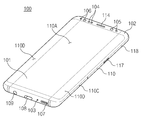
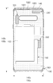
도 1 및 2를 참조하면, 일 실시 예에 따른 전자 장치(100)는, 제 1 면(또는 전면)(110A), 제 2 면(또는 후면)(110B), 및 제 1 면(110A) 및 제 2 면(110B) 사이의 공간을 둘러싸는 측면(110C)을 포함하는 하우징(110)을 포함할 수 있다. 다른 실시 예(미도시)에서는, 하우징은, 도 1의 제 1 면(110A), 제 2 면(110B) 및 측면(110C)들 중 일부를 형성하는 구조를 지칭할 수도 있다. 일 실시 예에 따르면, 제 1 면(110A)은 적어도 일부분이 실질적으로 투명한 전면 플레이트(102)(예: 다양한 코팅 레이어들을 포함하는 글라스 플레이트, 또는 폴리머 플레이트)에 의하여 형성될 수 있다. 제 2 면(110B)은 실질적으로 불투명한 후면 플레이트(111)에 의하여 형성될 수 있다. 상기 후면 플레이트(111)는, 예를 들어, 코팅 또는 착색된 유리, 세라믹, 폴리머, 금속(예: 알루미늄, 스테인레스 스틸(STS), 또는 마그네슘), 또는 상기 물질들 중 적어도 둘의 조합에 의하여 형성될 수 있다. 상기 측면(110C)은, 전면 플레이트(102) 및 후면 플레이트(111)와 결합하며, 금속 및/또는 폴리머를 포함하는 측면 베젤 구조 (또는 "측면 부재")(118)에 의하여 형성될 수 있다. 어떤 실시 예에서는, 후면 플레이트(111) 및 측면 베젤 구조(118)는 일체로 형성되고 동일한 물질(예: 알루미늄과 같은 금속 물질)을 포함할 수 있다.1 and 2, the
도시된 실시 예에서는, 상기 전면 플레이트(102)는, 상기 제 1 면(110A)으로부터 상기 후면 플레이트(111) 쪽으로 휘어져 심리스하게(seamless) 연장된 2개의 제 1 영역(110D)들을, 상기 전면 플레이트(102)의 긴 엣지(long edge) 양단에 포함할 수 있다. 도시된 실시 예(도 2 참조)에서, 상기 후면 플레이트(111)는, 상기 제 2 면(110B)으로부터 상기 전면 플레이트(102) 쪽으로 휘어져 심리스하게 연장된 2개의 제 2 영역(110E)들을 긴 엣지 양단에 포함할 수 있다. 어떤 실시 예에서는, 상기 전면 플레이트(102)(또는 상기 후면 플레이트(111))가 상기 제 1 영역(110D)들(또는 상기 제 2 영역(110E)들) 중 하나 만을 포함할 수 있다. 다른 실시 예에서는, 상기 제 1 영역(110D)들 또는 제 2 영역(110E)들 중 일부가 포함되지 않을 수 있다. 상기 실시 예들에서, 상기 전자 장치(100)의 측면에서 볼 때, 측면 베젤 구조(118)는, 상기와 같은 제 1 영역(110D)들 또는 제 2 영역(110E)들이 포함되지 않는 측면 쪽에서는 제 1 두께(또는 폭)을 가지고, 상기 제 1 영역(110D)들 또는 제 2 영역(110E)들을 포함한 측면 쪽에서는 상기 제 1 두께보다 얇은 제 2 두께를 가질 수 있다.In the illustrated embodiment, the
일 실시 예에 따르면, 전자 장치(100)는, 디스플레이(101), 오디오 모듈(103, 107, 114), 센서 모듈(104, 116, 119), 카메라 모듈(105, 112, 113), 키 입력 장치(117), 발광 소자(106), 및 커넥터 홀(108, 109) 중 적어도 하나 이상을 포함할 수 있다. 어떤 실시 예에서는, 전자 장치(100)는, 구성요소들 중 적어도 하나(예: 키 입력 장치(117), 또는 발광 소자(106))를 생략하거나 다른 구성요소를 추가적으로 포함할 수 있다.According to one embodiment, the
디스플레이(101)는, 예를 들어, 전면 플레이트(102)의 상당 부분을 통하여 노출될 수 있다. 어떤 실시 예에서는, 상기 제 1 면(110A), 및 상기 측면(110C)의 제 1 영역(110D)들을 형성하는 전면 플레이트(102)를 통하여 상기 디스플레이(101)의 적어도 일부가 노출될 수 있다. 어떤 실시 예에서는, 디스플레이(101)의 모서리를 상기 전면 플레이트(102)의 인접한 외곽 형상과 대체로 동일하게 형성할 수 있다. 다른 실시 예(미도시)에서는, 디스플레이(101)가 노출되는 면적을 확장하기 위하여, 디스플레이(101)의 외곽과 전면 플레이트(102)의 외곽간의 간격이 대체로 동일하게 형성될 수 있다.The
다른 실시 예(미도시)에서는, 디스플레이(101)의 화면 표시 영역의 일부에 리세스 또는 개구부(opening)을 형성하고, 상기 리세스 또는 상기 개구부(opening)와 정렬되는 오디오 모듈(114), 센서 모듈(104), 카메라 모듈(105), 및 발광 소자(106) 중 적어도 하나 이상을 포함할 수 있다. 다른 실시 예(미도시)에서는, 디스플레이(101)의 화면 표시 영역의 배면에, 오디오 모듈(114), 센서 모듈(104), 카메라 모듈(105), 지문 센서(116), 및 발광 소자(106) 중 적어도 하나 이상을 포함할 수 있다. 다른 실시 예(미도시)에서는, 디스플레이(101)는, 터치 감지 회로, 터치의 세기(압력)를 측정할 수 있는 압력 센서, 및/또는 자기장 방식의 스타일러스 펜을 검출하는 디지타이저와 결합되거나 인접하여 배치될 수 있다. 어떤 실시 예에서는, 상기 센서 모듈(104, 119)의 적어도 일부, 및/또는 키 입력 장치(117)의 적어도 일부가, 상기 제 1 영역(110D)들, 및/또는 상기 제 2 영역(110E)들에 배치될 수 있다. In another embodiment (not shown), a recess or opening is formed in a part of a screen display area of the
오디오 모듈(103, 107, 114)은, 마이크 홀(103) 및 스피커 홀(107, 114)을 포함할 수 있다. 마이크 홀(103)은 외부의 소리를 획득하기 위한 마이크가 내부에 배치될 수 있고, 어떤 실시 예에서는 소리의 방향을 감지할 수 있도록 복수개의 마이크가 배치될 수 있다. 스피커 홀(107, 114)은, 외부 스피커 홀(107) 및 통화용 리시버 홀(114)을 포함할 수 있다. 어떤 실시 예에서는 스피커 홀(107, 114)과 마이크 홀(103)이 하나의 홀로 구현 되거나, 스피커 홀(107, 114) 없이 스피커가 포함될 수 있다(예: 피에조 스피커). The
센서 모듈(104, 116, 119)은, 전자 장치(100)의 내부의 작동 상태, 또는 외부의 환경 상태에 대응하는 전기 신호 또는 데이터 값을 생성할 수 있다. 센서 모듈(104, 116, 119)은, 예를 들어, 하우징(110)의 제 1 면(110A)에 배치된 제 1 센서 모듈(104)(예: 근접 센서) 및/또는 제 2 센서 모듈(미도시)(예: 지문 센서), 및/또는 상기 하우징(110)의 제 2 면(110B)에 배치된 제 3 센서 모듈(119)(예: HRM 센서) 및/또는 제 4 센서 모듈(116) (예: 지문 센서)을 포함할 수 있다. 상기 지문 센서는 하우징(110)의 제 1면(110A)(예: 디스플레이(101) 뿐만 아니라 제 2면(110B)에 배치될 수 있다. 전자 장치(100)는, 도시되지 않은 센서 모듈, 예를 들어, 제스처 센서, 자이로 센서, 기압 센서, 마그네틱 센서, 가속도 센서, 그립 센서, 컬러 센서, IR(infrared) 센서, 생체 센서, 온도 센서, 습도 센서, 또는 조도 센서(104) 중 적어도 하나를 더 포함할 수 있다.The
카메라 모듈(105, 112, 113)은, 전자 장치(100)의 제 1 면(110A)에 배치된 제 1 카메라 장치(105), 및 제 2 면(110B)에 배치된 제 2 카메라 장치(112), 및/또는 플래시(113)를 포함할 수 있다. 상기 카메라 장치들(105, 112)은, 하나 또는 복수의 렌즈들, 이미지 센서, 및/또는 이미지 시그널 프로세서를 포함할 수 있다. 플래시(113)는, 예를 들어, 발광 다이오드 또는 제논 램프(xenon lamp)를 포함할 수 있다. 어떤 실시 예에서는, 2개 이상의 렌즈들(적외선 카메라, 광각 및 망원 렌즈) 및 이미지 센서들이 전자 장치(100)의 한 면에 배치될 수 있다.The
키 입력 장치(117)는, 하우징(110)의 측면(110C)에 배치될 수 있다. 다른 실시 예에서는, 전자 장치(100)는 상기 언급된 키 입력 장치(117) 중 일부 또는 전부를 포함하지 않을 수 있고 포함되지 않은 키 입력 장치(117)는 디스플레이(101) 상에 소프트 키 등 다른 형태로 구현될 수 있다. 어떤 실시 예에서, 키 입력 장치는 하우징(110)의 제 2면(110B)에 배치된 센서 모듈(116)을 포함할 수 있다.
The
발광 소자(106)는, 예를 들어, 하우징(110)의 제 1 면(110A)에 배치될 수 있다. 발광 소자(106)는, 예를 들어, 전자 장치(100)의 상태 정보를 광 형태로 제공할 수 있다. 다른 실시 예에서는, 발광 소자(106)는, 예를 들어, 카메라 모듈(105)의 동작과 연동되는 광원을 제공할 수 있다. 발광 소자(106)는, 예를 들어, LED, IR LED 및 제논 램프를 포함할 수 있다.The
커넥터 홀(108, 109)은, 외부 전자 장치와 전력 및/또는 데이터를 송수신하기 위한 커넥터(예를 들어, USB 커넥터)를 수용할 수 있는 제 1 커넥터 홀(108), 및/또는 외부 전자 장치와 오디오 신호를 송수신하기 위한 커넥터를 수용할 수 있는 제 2 커넥터 홀(예를 들어, 이어폰 잭)(109)을 포함할 수 있다.
The connector holes 108 and 109 include a
도 3을 참조하면, 전자 장치(100)는, 측면 베젤 구조(140), 제1 지지 부재(142)(예 : 브라켓), 전면 플레이트(120), 디스플레이(130), 인쇄 회로 기판(150), 배터리(152), 제 2 지지 부재(160)(예 : 리어 케이스), 안테나(170), 및 후면 플레이트(180)를 포함할 수 있다. 어떤 실시 예에서는, 전자 장치(100)는, 구성요소들 중 적어도 하나(예: 제1 지지 부재(142), 또는 제 2 지지 부재(160))를 생략하거나 다른 구성요소를 추가적으로 포함할 수 있다. 전자 장치(100)의 구성요소들 중 적어도 하나는, 도 1, 또는 도 2의 전자 장치(100)의 구성요소들 중 적어도 하나와 동일, 또는 유사할 수 있으며, 중복되는 설명은 이하 생략한다.Referring to FIG. 3, the
제1 지지 부재(142)는, 전자 장치(100) 내부에 배치되어 측면 베젤 구조(140)와 연결될 수 있거나, 측면 베젤 구조(140)와 일체로 형성될 수 있다. 제1 지지 부재(142)는, 예를 들어, 금속 재질 및/또는 비금속 (예: 폴리머) 재질로 형성될 수 있다. 제1 지지 부재(142)는, 일면에 디스플레이(130)가 결합되고 타면에 인쇄 회로 기판(150)이 결합될 수 있다. 인쇄 회로 기판(150)에는, 프로세서, 메모리, 및/또는 인터페이스가 장착될 수 있다. 프로세서는, 예를 들어, 중앙처리장치, 어플리케이션 프로세서, 그래픽 처리 장치, 이미지 시그널 프로세서, 센서 허브 프로세서, 또는 커뮤니케이션 프로세서 중 하나 또는 그 이상을 포함할 수 있다.The
메모리는, 예를 들어, 휘발성 메모리 또는 비휘발성 메모리를 포함할 수 있다. The memory may include, for example, volatile memory or nonvolatile memory.
인터페이스는, 예를 들어, HDMI(high definition multimedia interface), USB(universal serial bus) 인터페이스, SD카드 인터페이스, 및/또는 오디오 인터페이스를 포함할 수 있다. 인터페이스는, 예를 들어, 전자 장치(100)를 외부 전자 장치와 전기적 또는 물리적으로 연결시킬 수 있으며, USB 커넥터, SD 카드/MMC 커넥터, 또는 오디오 커넥터를 포함할 수 있다.The interface may include, for example, a high definition multimedia interface (HDMI), a universal serial bus (USB) interface, an SD card interface, and / or an audio interface. The interface may electrically or physically connect the
배터리(152)는 전자 장치(100)의 적어도 하나의 구성 요소에 전력을 공급하기 위한 장치로서, 예를 들면, 재충전 불가능한 1차 전지, 또는 재충전 가능한 2차 전지, 또는 연료 전지를 포함할 수 있다. 배터리(152)의 적어도 일부는, 예를 들어, 인쇄 회로 기판(150)과 실질적으로 동일 평면 상에 배치될 수 있다. 배터리(152)는 전자 장치(100) 내부에 일체로 배치될 수 있고, 전자 장치(100)와 탈부착 가능하게 배치될 수도 있다.The
안테나(170)는, 후면 플레이트(180)와 배터리(152) 사이에 배치될 수 있다. 안테나(170)는, 예를 들어, NFC(near field communication) 안테나, 무선 충전 안테나, 및/또는 MST(magnetic secure transmission) 안테나를 포함할 수 있다. 안테나(170)는, 예를 들어, 외부 장치와 근거리 통신을 하거나, 충전에 필요한 전력을 무선으로 송수신 할 수 있다. 다른 실시 예에서는, 측면 베젤 구조(140) 및/또는 상기 제1 지지 부재(142)의 일부 또는 그 조합에 의하여 안테나 구조가 형성될 수 있다.The
도 4은, 다양한 실시 예들에 따른, 네트워크 환경(400) 내의 전자 장치(401)의 블럭도이다. 도 4을 참조하면, 네트워크 환경(400)에서 전자 장치(401)는 제 1 네트워크(498)(예: 근거리 무선 통신 네트워크)를 통하여 전자 장치(402)와 통신하거나, 또는 제 2 네트워크(499)(예: 원거리 무선 통신 네트워크)를 통하여 전자 장치(404) 또는 서버(408)와 통신할 수 있다. 일 실시 예에 따르면, 전자 장치(401)는 서버(408)를 통하여 전자 장치(404)와 통신할 수 있다. 일 실시 예에 따르면, 전자 장치(401)는 프로세서(420), 메모리(430), 입력 장치(450), 음향 출력 장치(455), 표시 장치(460), 오디오 모듈(470), 센서 모듈(476), 인터페이스(477), 햅틱 모듈(479), 카메라 모듈(480), 전력 관리 모듈(488), 배터리(489), 통신 모듈(490), 가입자 식별 모듈(496), 또는 안테나 모듈(497)을 포함할 수 있다. 어떤 실시 예에서는, 전자 장치(401)에는, 이 구성요소들 중 적어도 하나(예: 표시 장치(460) 또는 카메라 모듈(480))가 생략되거나, 하나 이상의 다른 구성 요소가 추가될 수 있다. 어떤 실시 예에서는, 이 구성요소들 중 일부들은 하나의 통합된 회로로 구현될 수 있다. 예를 들면, 센서 모듈(476)(예: 지문 센서, 홍채 센서, 또는 조도 센서)은 표시 장치(460)(예: 디스플레이)에 임베디드된 채 구현될 수 있다4 is a block diagram of an electronic device 401 in a
프로세서(420)는, 예를 들면, 소프트웨어(예: 프로그램(440))를 실행하여 프로세서(420)에 연결된 전자 장치(401)의 적어도 하나의 다른 구성요소(예: 하드웨어 또는 소프트웨어 구성요소)을 제어할 수 있고, 다양한 데이터 처리 또는 연산을 수행할 수 있다. 일 실시 예에 따르면, 데이터 처리 또는 연산의 적어도 일부로서, 프로세서(420)는 다른 구성요소(예: 센서 모듈(476) 또는 통신 모듈(490))로부터 수신된 명령 또는 데이터를 휘발성 메모리(432)에 로드하고, 휘발성 메모리(432)에 저장된 명령 또는 데이터를 처리하고, 결과 데이터를 비휘발성 메모리(434)에 저장할 수 있다. 일 실시 예에 따르면, 프로세서(420)는 메인 프로세서(421)(예: 중앙 처리 장치 또는 어플리케이션 프로세서), 및 이와는 독립적으로 또는 함께 운영 가능한 보조 프로세서(423)(예: 그래픽 처리 장치, 이미지 시그널 프로세서, 센서 허브 프로세서, 또는 커뮤니케이션 프로세서)를 포함할 수 있다. 추가적으로 또는 대체적으로, 보조 프로세서(423)은 메인 프로세서(421)보다 저전력을 사용하거나, 또는 지정된 기능에 특화되도록 설정될 수 있다. 보조 프로세서(423)는 메인 프로세서(421)와 별개로, 또는 그 일부로서 구현될 수 있다.The processor 420, for example, executes software (eg, the program 440) to execute at least one other component (eg, hardware or software component) of the electronic device 401 connected to the processor 420. It can be controlled and can perform various data processing or operations. According to an embodiment, as at least a part of data processing or operation, the processor 420 may receive instructions or data received from other components (eg, the
보조 프로세서(423)는, 예를 들면, 메인 프로세서(421)가 인액티브(예: 슬립) 상태에 있는 동안 메인 프로세서(421)를 대신하여, 또는 메인 프로세서(421)가 액티브(예: 어플리케이션 실행) 상태에 있는 동안 메인 프로세서(421)와 함께, 전자 장치(401)의 구성요소들 중 적어도 하나의 구성요소(예: 표시 장치(460), 센서 모듈(476), 또는 통신 모듈(490))와 관련된 기능 또는 상태들의 적어도 일부를 제어할 수 있다. 일 실시 예에 따르면, 보조 프로세서(423)(예: 이미지 시그널 프로세서 또는 커뮤니케이션 프로세서)는 기능적으로 관련 있는 다른 구성 요소(예: 카메라 모듈(480) 또는 통신 모듈(490))의 일부로서 구현될 수 있다. The
메모리(430)는, 전자 장치(401)의 적어도 하나의 구성요소(예: 프로세서(420) 또는 센서모듈(476))에 의해 사용되는 다양한 데이터를 저장할 수 있다. 데이터는, 예를 들어, 소프트웨어(예: 프로그램(440)) 및, 이와 관련된 명령에 대한 입력 데이터 또는 출력 데이터를 포함할 수 있다. 메모리(430)는, 휘발성 메모리(432) 또는 비휘발성 메모리(434)를 포함할 수 있다. The memory 430 may store various data used by at least one component of the electronic device 401 (eg, the processor 420 or the sensor module 476). The data may include, for example, software (eg, the program 440) and input data or output data for commands related thereto. The memory 430 may include a volatile memory 432 or a nonvolatile memory 434.
프로그램(440)은 메모리(430)에 소프트웨어로서 저장될 수 있으며, 예를 들면, 운영 체제(442), 미들 웨어(444) 또는 어플리케이션(446)을 포함할 수 있다. The program 440 may be stored as software in the memory 430, and may include, for example, an operating system 442, middleware 444, or an application 446.
입력 장치(450)는, 전자 장치(401)의 구성요소(예: 프로세서(420))에 사용될 명령 또는 데이터를 전자 장치(401)의 외부(예: 사용자)로부터 수신할 수 있다. 입력 장치(450)은, 예를 들면, 마이크, 마우스, 키보드, 또는 디지털 펜(예:스타일러스 펜)을 포함할 수 있다. The
음향 출력 장치(455)는 음향 신호를 전자 장치(401)의 외부로 출력할 수 있다. 음향 출력 장치(455)는, 예를 들면, 스피커 또는 리시버를 포함할 수 있다. 스피커는 멀티미디어 재생 또는 녹음 재생과 같이 일반적인 용도로 사용될 수 있고, 리시버는 착신 전화를 수신하기 위해 사용될 수 있다. 일 실시 예에 따르면, 리시버는 스피커와 별개로, 또는 그 일부로서 구현될 수 있다.The
표시 장치(460)는 전자 장치(401)의 외부(예: 사용자)로 정보를 시각적으로 제공할 수 있다. 표시 장치(460)은, 예를 들면, 디스플레이, 홀로그램 장치, 또는 프로젝터 및 해당 장치를 제어하기 위한 제어 회로를 포함할 수 있다. 일 실시 예에 따르면, 표시 장치(460)는 터치를 감지하도록 설정된 터치 회로(touch circuitry), 또는 상기 터치에 의해 발생되는 힘의 세기를 측정하도록 설정된 센서 회로(예: 압력 센서)를 포함할 수 있다. The display device 460 may visually provide information to the outside of the electronic device 401 (eg, a user). The display device 460 may include, for example, a display, a hologram device, or a projector and a control circuit for controlling the device. According to an embodiment, the display device 460 may include a touch circuitry configured to sense a touch, or a sensor circuit (eg, a pressure sensor) configured to measure the strength of the force generated by the touch. have.
오디오 모듈(470)은 소리를 전기 신호로 변환시키거나, 반대로 전기 신호를 소리로 변환시킬 수 있다. 일 실시 예에 따르면, 오디오 모듈(470)은, 입력 장치(450) 를 통해 소리를 획득하거나, 음향 출력 장치(455), 또는 전자 장치(401)와 직접 또는 무선으로 연결된 외부 전자 장치(예: 전자 장치(402)) (예: 스피커 또는 헤드폰))를 통해 소리를 출력할 수 있다.The audio module 470 may convert sound into an electrical signal, or vice versa. According to an embodiment of the present disclosure, the audio module 470 acquires sound through the
센서 모듈(476)은 전자 장치(401)의 작동 상태(예: 전력 또는 온도), 또는 외부의 환경 상태(예: 사용자 상태)를 감지하고, 감지된 상태에 대응하는 전기 신호 또는 데이터 값을 생성할 수 있다. 일 실시 예에 따르면, 센서 모듈(476)은, 예를 들면, 제스처 센서, 자이로 센서, 기압 센서, 마그네틱 센서, 가속도 센서, 그립 센서, 근접 센서, 컬러 센서, IR(infrared) 센서, 생체 센서, 온도 센서, 습도 센서, 또는 조도 센서를 포함할 수 있다. The
인터페이스(477)는 전자 장치(401)이 외부 전자 장치(예: 전자 장치(402))와 직접 또는 무선으로 연결되기 위해 사용될 수 있는 하나 이상의 지정된 프로토콜들을 지원할 수 있다. 일 실시 예에 따르면, 인터페이스(477)는, 예를 들면, HDMI(high definition multimedia interface), USB(universal serial bus) 인터페이스, SD카드 인터페이스, 또는 오디오 인터페이스를 포함할 수 있다.The
연결 단자(478)는, 그를 통해서 전자 장치(401)가 외부 전자 장치(예: 전자 장치(402))와 물리적으로 연결될 수 있는 커넥터를 포함할 수 있다. 일 실시 예에 따르면, 연결 단자(478)은, 예를 들면, HDMI 커넥터, USB 커넥터, SD 카드 커넥터, 또는 오디오 커넥터(예: 헤드폰 커넥터)를 포함할 수 있다.The
햅틱 모듈(479)은 전기적 신호를 사용자가 촉각 또는 운동 감각을 통해서 인지할 수 있는 기계적인 자극(예: 진동 또는 움직임) 또는 전기적인 자극으로 변환할 수 있다. 일 실시 예에 따르면, 햅틱 모듈(479)은, 예를 들면, 모터, 압전 소자, 또는 전기 자극 장치를 포함할 수 있다.The haptic module 479 may convert electrical signals into mechanical stimuli (eg, vibration or movement) or electrical stimuli that the user can perceive through tactile or motor sensations. According to one embodiment, the haptic module 479 may include, for example, a motor, a piezoelectric element, or an electrical stimulation device.
카메라 모듈(480)은 정지 영상 및 동영상을 촬영할 수 있다. 일 실시 예에 따르면, 카메라 모듈(480)은 하나 이상의 렌즈들, 이미지 센서들, 이미지 시그널 프로세서들, 또는 플래시들을 포함할 수 있다.The camera module 480 may capture still images and videos. According to one embodiment, the camera module 480 may include one or more lenses, image sensors, image signal processors, or flashes.
전력 관리 모듈(488)은 전자 장치(401)에 공급되는 전력을 관리할 수 있다. 일 실시 예에 따르면, 전력 관리 모듈(388)은, 예를 들면, PMIC(power management integrated circuit)의 적어도 일부로서 구현될 수 있다.The power management module 488 may manage power supplied to the electronic device 401. According to an embodiment, the power management module 388 may be implemented, for example, as at least a part of a power management integrated circuit (PMIC).
배터리(489)는 전자 장치(401)의 적어도 하나의 구성 요소에 전력을 공급할 수 있다. 일 실시 예에 따르면, 배터리(489)는, 예를 들면, 재충전 불가능한 1차 전지, 재충전 가능한 2차 전지 또는 연료 전지를 포함할 수 있다.The
통신 모듈(490)은 전자 장치(401)와 외부 전자 장치(예: 전자 장치(402), 전자 장치(404), 또는 서버(408))간의 직접(예: 유선) 통신 채널 또는 무선 통신 채널의 수립, 및 수립된 통신 채널을 통한 통신 수행을 지원할 수 있다. 통신 모듈(490)은 프로세서(420)(예: 어플리케이션 프로세서)와 독립적으로 운영되고, 직접(예: 유선) 통신 또는 무선 통신을 지원하는 하나 이상의 커뮤니케이션 프로세서를 포함할 수 있다. 일 실시 예에 따르면, 통신 모듈(490)은 무선 통신 모듈(492)(예: 셀룰러 통신 모듈, 근거리 무선 통신 모듈, 또는 GNSS(global navigation satellite system) 통신 모듈) 또는 유선 통신 모듈(494)(예: LAN(local area network) 통신 모듈, 또는 전력선 통신 모듈)을 포함할 수 있다. 이들 통신 모듈 중 해당하는 통신 모듈은 제 1 네트워크(498)(예: 블루투스, WiFi direct 또는 IrDA(infrared data association) 같은 근거리 통신 네트워크) 또는 제 2 네트워크(499)(예: 셀룰러 네트워크, 인터넷, 또는 컴퓨터 네트워크(예: LAN 또는 WAN)와 같은 원거리 통신 네트워크)를 통하여 외부 전자 장치와 통신할 수 있다. 이런 여러 종류의 통신 모듈들은 하나의 구성 요소(예: 단일 칩)으로 통합되거나, 또는 서로 별도의 복수의 구성 요소들(예: 복수 칩들)로 구현될 수 있다. 무선 통신 모듈(492)은 가입자 식별 모듈(496)에 저장된 가입자 정보(예: 국제 모바일 가입자 식별자(IMSI))를 이용하여 제 1 네트워크(498) 또는 제 2 네트워크(499)와 같은 통신 네트워크 내에서 전자 장치(401)를 확인 및 인증할 수 있다. The communication module 490 is a direct (eg, wired) communication channel or wireless communication channel between the electronic device 401 and an external electronic device (eg, the
안테나 모듈(497)은 신호 또는 전력을 외부(예: 외부 전자 장치)로 송신하거나 외부로부터 수신할 수 있다. 일 실시 예에 따르면, 안테나 모듈은 서브스트레이트(예: PCB) 위에 형성된 도전체 또는 도전성 패턴으로 이루어진 방사체를 포함하는 하나의 안테나를 포함할 수 있다. 일 실시 예에 따르면, 안테나 모듈(497)은 복수의 안테나들을 포함할 수 있다. 이런 경우, 제 1 네트워크(498) 또는 제 2 네트워크(499)와 같은 통신 네트워크에서 사용되는 통신 방식에 적합한 적어도 하나의 안테나가, 예를 들면, 통신 모듈(490)에 의하여 상기 복수의 안테나들로부터 선택될 수 있다. 신호 또는 전력은 상기 선택된 적어도 하나의 안테나를 통하여 통신 모듈(490)과 외부 전자 장치 간에 송신되거나 수신될 수 있다. 어떤 실시 예에 따르면, 방사체 이외에 다른 부품(예: RFIC)이 추가로 안테나 모듈(497)의 일부로 형성될 수 있다.The
상기 구성요소들 중 적어도 일부는 주변 기기들간 통신 방식(예: 버스, GPIO(general purpose input and output), SPI(serial peripheral interface), 또는 MIPI(mobile industry processor interface))를 통해 서로 연결되고 신호(예: 명령 또는 데이터)를 상호간에 교환할 수 있다.At least some of the components are connected to each other through a communication method between peripheral devices (for example, a bus, a general purpose input and output (GPIO), a serial peripheral interface (SPI), or a mobile industry processor interface (MIPI)) and a signal ( Ex: command or data) can be exchanged with each other.
일 실시 예에 따르면, 명령 또는 데이터는 제 2 네트워크(499)에 연결된 서버(408)를 통해서 전자 장치(401)와 외부의 전자 장치(404)간에 송신 또는 수신될 수 있다. 전자 장치(402, 404) 각각은 전자 장치(401)와 동일한 또는 다른 종류의 장치일 수 있다. 일 실시 예에 따르면, 전자 장치(401)에서 실행되는 동작들의 전부 또는 일부는 외부 전자 장치들(402, 404, or 408) 중 하나 이상의 외부 장치들에서 실행될 수 있다. 예를 들면, 전자 장치(401)가 어떤 기능이나 서비스를 자동으로, 또는 사용자 또는 다른 장치로부터의 요청에 반응하여 수행해야 할 경우에, 전자 장치(401)는 기능 또는 서비스를 자체적으로 실행시키는 대신에 또는 추가적으로, 하나 이상의 외부 전자 장치들에게 그 기능 또는 그 서비스의 적어도 일부를 수행하라고 요청할 수 있다. 상기 요청을 수신한 하나 이상의 외부 전자 장치들은 요청된 기능 또는 서비스의 적어도 일부, 또는 상기 요청과 관련된 추가 기능 또는 서비스를 실행하고, 그 실행의 결과를 전자 장치(401)로 전달할 수 있다. 전자 장치(401)는 상기 결과를, 그대로 또는 추가적으로 처리하여, 상기 요청에 대한 응답의 적어도 일부로서 제공할 수 있다.. 이를 위하여, 예를 들면, 클라우드 컴퓨팅, 분산 컴퓨팅, 또는 클라이언트-서버 컴퓨팅 기술이 이용될 수 있다. According to an embodiment, the command or data may be transmitted or received between the electronic device 401 and an external
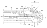
도 5는 다양한 실시 예들에 따른, 레거시 네트워크 통신 및 5G 네트워크 통신을 지원하기 위한 전자 장치(401)의 블록도(500)이다. 도 5를 참조하면, 전자 장치(401)는 제 1 커뮤니케이션 프로세서(512), 제 2 커뮤니케이션 프로세서(514), 제 1 radio frequency integrated circuit(RFIC)(522), 제 2 RFIC(524), 제 3 RFIC(526), 제 4 RFIC(528), 제 1 radio frequency front end(RFFE)(532), 제 2 RFFE(534), 제 1 안테나 모듈(542), 제 2 안테나 모듈(544), 및 안테나(548)을 포함할 수 있다. 전자 장치(401)는 프로세서(420) 및 메모리(430)를 더 포함할 수 있다. 네트워크(499)는 제 1 네트워크(592)와 제2 네트워크(594)를 포함할 수 있다. 다른 실시 예에 따르면, 전자 장치(401)는 도4에 기재된 부품들 중 적어도 하나의 부품을 더 포함할 수 있고, 네트워크(499)는 적어도 하나의 다른 네트워크를 더 포함할 수 있다. 일 실시 예에 따르면, 제 1 커뮤니케이션 프로세서(512), 제 2 커뮤니케이션 프로세서(514), 제 1 RFIC(522), 제 2 RFIC(524), 제 4 RFIC(528), 제 1 RFFE(532), 및 제 2 RFFE(534)는 무선 통신 모듈(492)의 적어도 일부를 형성할 수 있다. 다른 실시 예에 따르면, 제 4 RFIC(528)는 생략되거나, 제 3 RFIC(526)의 일부로서 포함될 수 있다. 5 is a block diagram 500 of an electronic device 401 for supporting legacy network communication and 5G network communication, according to various embodiments. Referring to FIG. 5, the electronic device 401 includes a first communication processor 512, a second communication processor 514, a first radio frequency integrated circuit (RFIC) 522, a
제 1 커뮤니케이션 프로세서(512)는 제 1 네트워크(592)와의 무선 통신에 사용될 대역의 통신 채널의 수립, 및 수립된 통신 채널을 통한 레거시 네트워크 통신을 지원할 수 있다. 다양한 실시 예들에 따르면, 제 1 네트워크는 2세대(2G), 3G, 4G, 또는 long term evolution(LTE) 네트워크를 포함하는 레거시 네트워크일 수 있다. 제 2 커뮤니케이션 프로세서(514)는 제 2 네트워크(594)와의 무선 통신에 사용될 대역 중 지정된 대역(예: 약 6GHz ~ 약 60GHz)에 대응하는 통신 채널의 수립, 및 수립된 통신 채널을 통한 5G 네크워크 통신을 지원할 수 있다. 다양한 실시 예들에 따르면, 제 2 네트워크(594)는 3GPP에서 정의하는 5G 네트워크일 수 있다. 추가적으로, 일 실시 예에 따르면, 제 1 커뮤니케이션 프로세서(512) 또는 제 2 커뮤니케이션 프로세서(514)는 제 2 네트워크(594)와의 무선 통신에 사용될 대역 중 다른 지정된 대역(예: 약 6GHz 이하)에 대응하는 통신 채널의 수립, 및 수립된 통신 채널을 통한 5G 네크워크 통신을 지원할 수 있다. 일 실시 예에 따르면, 제 1 커뮤니케이션 프로세서(512)와 제 2 커뮤니케이션 프로세서(514)는 단일(single) 칩 또는 단일 패키지 내에 구현될 수 있다. 다양한 실시 예들에 따르면, 제 1 커뮤니케이션 프로세서(512) 또는 제 2 커뮤니케이션 프로세서(514)는 프로세서(420), 보조 프로세서(423), 또는 통신 모듈(490)과 단일 칩 또는 단일 패키지 내에 형성될 수 있다.The first communication processor 512 may support establishment of a communication channel in a band to be used for wireless communication with the
제 1 RFIC(522)는, 송신 시에, 제 1 커뮤니케이션 프로세서(512)에 의해 생성된 기저대역(baseband) 신호를 제 1 네트워크(592)(예: 레거시 네트워크)에 사용되는 약 700MHz 내지 약 3GHz의 라디오 주파수(RF) 신호로 변환할 수 있다. 수신 시에는, RF 신호가 안테나(예: 제 1 안테나 모듈(542))를 통해 제 1 네트워크(592)(예: 레거시 네트워크)로부터 획득되고, RFFE(예: 제 1 RFFE(532))를 통해 전처리(preprocess)될 수 있다. 제 1 RFIC(522)는 전처리된 RF 신호를 제 1 커뮤니케이션 프로세서(512)에 의해 처리될 수 있도록 기저대역 신호로 변환할 수 있다.The first RFIC 522 transmits a baseband signal generated by the first communication processor 512 at the time of transmission from about 700 MHz to about 3 GHz used in the first network 592 (eg, a legacy network). Can be converted into radio frequency (RF) signals. Upon reception, an RF signal is obtained from the first network 592 (e.g., legacy network) through an antenna (e.g., the first antenna module 542), and through an RFFE (e.g., first RFFE 532). It can be preprocessed. The first RFIC 522 may convert the preprocessed RF signal into a baseband signal so that it can be processed by the first communication processor 512.
제 2 RFIC(524)는, 송신 시에, 제 1 커뮤니케이션 프로세서(512) 또는 제 2 커뮤니케이션 프로세서(514)에 의해 생성된 기저대역 신호를 제 2 네트워크(594)(예: 5G 네트워크)에 사용되는 Sub6 대역(예: 약 6GHz 이하)의 RF 신호(이하, 5G Sub6 RF 신호)로 변환할 수 있다. 수신 시에는, 5G Sub6 RF 신호가 안테나(예: 제 2 안테나 모듈(544))를 통해 제 2 네트워크(594)(예: 5G 네트워크)로부터 획득되고, RFFE(예: 제 2 RFFE(534))를 통해 전처리될 수 있다. 제 2 RFIC(524)는 전처리된 5G Sub6 RF 신호를 제 1 커뮤니케이션 프로세서(512) 또는 제 2 커뮤니케이션 프로세서(514) 중 대응하는 커뮤니케이션 프로세서에 의해 처리될 수 있도록 기저대역 신호로 변환할 수 있다. The
제 3 RFIC(526)는 제 2 커뮤니케이션 프로세서(514)에 의해 생성된 기저대역 신호를 제 2 네트워크(594)(예: 5G 네트워크)에서 사용될 5G Above6 대역(예: 약 6GHz ~ 약 60GHz)의 RF 신호(이하, 5G Above6 RF 신호)로 변환할 수 있다. 수신 시에는, 5G Above6 RF 신호가 안테나(예: 안테나(548))를 통해 제 2 네트워크(594)(예: 5G 네트워크)로부터 획득되고 제 3 RFFE(536)를 통해 전처리될 수 있다. 제 3 RFIC(526)는 전처리된 5G Above 6 RF 신호를 제 2 커뮤니케이션 프로세서(514)에 의해 처리될 수 있도록 기저대역 신호로 변환할 수 있다. 일 실시 예에 따르면, 제 3 RFFE(536)는 제 3 RFIC(526)의 일부로서 형성될 수 있다.The
전자 장치(401)는, 일 실시 예에 따르면, 제 3 RFIC(526)와 별개로 또는 적어도 그 일부로서, 제 4 RFIC(528)를 포함할 수 있다. 이런 경우, 제 4 RFIC(528)는 제 2 커뮤니케이션 프로세서(514)에 의해 생성된 기저대역 신호를 중간(intermediate) 주파수 대역(예: 약 9GHz ~ 약 11GHz)의 RF 신호(이하, IF 신호)로 변환한 뒤, 상기 IF 신호를 제 3 RFIC(526)로 전달할 수 있다. 제 3 RFIC(526)는 IF 신호를 5G Above6 RF 신호로 변환할 수 있다. 수신 시에, 5G Above6 RF 신호가 안테나(예: 안테나(548))를 통해 제 2 네트워크(594)(예: 5G 네트워크)로부터 수신되고 제 3 RFIC(526)에 의해 IF 신호로 변환될 수 있다. 제 4 RFIC(528)는 IF 신호를 제 2 커뮤니케이션 프로세서(514)가 처리할 수 있도록 기저대역 신호로 변환할 수 있다.The electronic device 401 may include the
일 실시 예에 따르면, 제 1 RFIC(522)와 제 2 RFIC(524)는 단일 칩 또는 단일 패키지의 적어도 일부로 구현될 수 있다. 일 실시 예에 따르면, 제 1 RFFE(532)와 제 2 RFFE(534)는 단일 칩 또는 단일 패키지의 적어도 일부로 구현될 수 있다. 일 실시 예에 따르면, 제 1 안테나 모듈(542) 또는 제 2 안테나 모듈(544)중 적어도 하나의 안테나 모듈은 생략되거나 다른 안테나 모듈과 결합되어 대응하는 복수의 대역들의 RF 신호들을 처리할 수 있다.According to an embodiment, the first RFIC 522 and the
일 실시 예에 따르면, 제 3 RFIC(526)와 안테나(548)는 동일한 서브스트레이트에 배치되어 제 3 안테나 모듈(546)을 형성할 수 있다. 예를 들어, 무선 통신 모듈(492) 또는 프로세서(420)가 제 1 서브스트레이트(예: main PCB)에 배치될 수 있다. 이런 경우, 제 1 서브스트레이트와 별도의 제 2 서브스트레이트(예: sub PCB)의 일부 영역(예: 하면)에 제 3 RFIC(526)가, 다른 일부 영역(예: 상면)에 안테나(548)가 배치되어, 제 3 안테나 모듈(546)이 형성될 수 있다. 일 실시 예에 따르면, 안테나(548)는, 예를 들면, 빔포밍에 사용될 수 있는 안테나 어레이를 포함할 수 있다. 제 3 RFIC(526)와 안테나(548)를 동일한 서브스트레이트에 배치함으로써 그 사이의 전송 선로의 길이를 줄이는 것이 가능하다. 이는, 예를 들면, 5G 네트워크 통신에 사용되는 고주파 대역(예: 약 6GHz ~ 약 60GHz)의 신호가 전송 선로에 의해 손실(예: 감쇄)되는 것을 줄일 수 있다. 이로 인해, 전자 장치(401)는 제 2 네트워크(594)(예: 5G 네트워크)와의 통신의 품질 또는 속도를 향상시킬 수 있다.According to an embodiment, the
제 2 네트워크(594)(예: 5G 네트워크)는 제 1 네트워크(592)(예: 레거시 네트워크)와 독립적으로 운영되거나(예: Stand-Alone (SA)), 연결되어 운영될 수 있다(예: Non-Stand Alone (NSA)). 예를 들면, 5G 네트워크에는 액세스 네트워크(예: 5G radio access network(RAN) 또는 next generation RAN(NG RAN))만 있고, 코어 네트워크(예: next generation core(NGC))는 없을 수 있다. 이런 경우, 전자 장치(401)는 5G 네트워크의 액세스 네트워크에 액세스한 후, 레거시 네트워크의 코어 네트워크(예: evolved packed core(EPC))의 제어 하에 외부 네트워크(예: 인터넷)에 액세스할 수 있다. 레거시 네트워크와 통신을 위한 프로토콜 정보(예: LTE 프로토콜 정보) 또는 5G 네트워크와 통신을 위한 프로토콜 정보(예: New Radio(NR) 프로토콜 정보)는 메모리(530)에 저장되어, 다른 부품(예: 프로세서(420), 제 1 커뮤니케이션 프로세서(512), 또는 제 2 커뮤니케이션 프로세서(514))에 의해 액세스될 수 있다.The second network 594 (eg, 5G network) may be operated independently of the first network 592 (eg, legacy network) (eg, Stand-Alone (SA)) or may be connected and operated (eg: Non-Stand Alone (NSA)). For example, a 5G network may have only an access network (eg, 5G radio access network (RAN) or next generation RAN (NG RAN)), and no core network (eg, next generation core (NGC)). In this case, the electronic device 401 may access the external network (eg, the Internet) under the control of the core network (eg, evolved packed core (EPC)) of the legacy network after accessing the access network of the 5G network. Protocol information (eg, LTE protocol information) for communication with a legacy network or protocol information (eg, New Radio (NR) protocol information) for communication with a 5G network is stored in the memory 530, and other components (eg, a processor) 420, the first communication processor 512, or the second communication processor 514).
도 6는, 예를 들어, 도 5를 참조하여 설명된 제 3 안테나 모듈(546)의 구조의 일 실시 예를 도시한다. 도 6a는, 상기 제 3 안테나 모듈(546)을 일측에서 바라본 사시도이고, 도 6b는 상기 제 3 안테나 모듈(546)을 다른 측에서 바라본 사시도이다. 도 6c는 상기 제 3 안테나 모듈(546)의 A-A'에 대한 단면도이다.FIG. 6 shows an embodiment of the structure of the
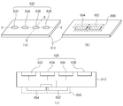
도 6을 참조하면, 일 실시 예에서, 제 3 안테나 모듈(546)은 인쇄회로기판(610), 안테나 어레이(630), RFIC(radio frequency integrate circuit)(652), PMIC(power manage integrate circuit)(654), 모듈 인터페이스(670)을 포함할 수 있다. 선택적으로, 제 3 안테나 모듈(546)은 차폐 부재(690)를 더 포함할 수 있다. 다른 실시 예들에서는, 상기 언급된 부품들 중 적어도 하나가 생략되거나, 상기 부품들 중 적어도 두 개가 일체로 형성될 수도 있다.Referring to FIG. 6, in one embodiment, the
인쇄회로기판(610)은 복수의 도전성 레이어들, 및 상기 도전성 레이어들과 교번하여 적층된 복수의 비도전성 레이어들을 포함할 수 있다. 상기 인쇄회로기판(610)은, 상기 도전성 레이어에 형성된 배선들 및 도전성 비아들을 이용하여 인쇄회로기판(610) 및/또는 외부에 배치된 다양한 전자 부품들 간 전기적 연결을 제공할 수 있다.The printed
안테나 어레이(630)(예를 들어, 도 5의 548)는, 방향성 빔을 형성하도록 배치된 복수의 안테나 엘리먼트들(632, 634, 636, 또는 638)을 포함할 수 있다. 상기 안테나 엘리먼트들은, 도시된 바와 같이 인쇄회로기판(610)의 제 1 면에 형성될 수 있다. 다른 실시 예에 따르면, 안테나 어레이(630)는 인쇄회로기판(610)의 내부에 형성될 수 있다. 실시 예들에 따르면, 안테나 어레이(630)는, 동일 또는 상이한 형상 또는 종류의 복수의 안테나 어레이들(예: 다이폴 안테나 어레이, 및/또는 패치 안테나 어레이)을 포함할 수 있다.The antenna array 630 (eg, 548 in FIG. 5) can include a plurality of
RFIC(652)(예를 들어, 도 5의 526)는, 상기 안테나 어레이와 이격된, 인쇄회로기판(610)의 다른 영역(예: 상기 제 1 면의 반대쪽인 제 2 면)에 배치될 수 있다. 상기 RFIC는, 안테나 어레이(630)를 통해 송/수신되는, 선택된 주파수 대역의 신호를 처리할 수 있도록 구성된다. 일 실시 예에 따르면, RFIC(652)는, 송신 시에, 통신 프로세서(미도시)로부터 획득된 기저대역 신호를 지정된 대역의 RF 신호로 변환할 수 있다. 상기 RFIC(652)는, 수신 시에, 안테나 어레이(652)를 통해 수신된 RF 신호를, 기저대역 신호로 변환하여 통신 프로세서에 전달할 수 있다.The RFIC 652 (eg, 526 in FIG. 5) can be placed in another area of the printed circuit board 610 (eg, the second side opposite the first side) spaced apart from the antenna array. have. The RFIC is configured to process signals of a selected frequency band, which are transmitted / received through the
다른 실시 예에 따르면, RFIC(652)는, 송신 시에, IFIC(intermediate frequency integrate circuit)(예를 들어, 도 5의 528)로부터 획득된 IF 신호(예: 약 9GHz ~ 약 11GHz) 를 선택된 대역의 RF 신호로 업 컨버트 할 수 있다. 상기 RFIC(652)는, 수신 시에, 안테나 어레이(652)를 통해 획득된 RF 신호를 다운 컨버트하여 IF 신호로 변환하여 상기 IFIC에 전달할 수 있다.According to another embodiment, the
PMIC(654)는, 상기 안테나 어레이와 이격된, 인쇄회로기판(610)의 다른 일부 영역(예: 상기 제 2 면)에 배치될 수 있다. PMIC는 메인 PCB(미도시)로부터 전압을 공급받아서, 안테나 모듈 상의 다양한 부품(예를 들어, RFIC(652))에 필요한 전원을 제공할 수 있다.The
차폐 부재(690)는 RFIC(652) 또는 PMIC(654) 중 적어도 하나를 전자기적으로 차폐하도록 상기 인쇄회로기판(610)의 일부(예를 들어, 상기 제 2 면)에 배치될 수 있다. 일 실시 예에 따르면, 차폐 부재(690)는 쉴드캔을 포함할 수 있다.The shielding
도시되지 않았으나, 다양한 실시 예들에서, 제 3 안테나 모듈(546)은, 모듈 인터페이스를 통해 다른 인쇄회로기판(예: 주 회로기판)과 전기적으로 연결될 수 있다. 상기 모듈 인터페이스는, 연결 부재, 예를 들어, 동축 케이블 커넥터, board to board 커넥터, 인터포저, 또는 FPCB(flexible printed circuit board)를 포함할 수 있다. 상기 연결 부재를 통하여, 상기 안테나 모듈의 RFIC(652) 및/또는 PMIC(654)가 상기 인쇄회로기판과 전기적으로 연결될 수 있다. Although not shown, in various embodiments, the
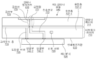
도 7는, 도 6의 (a) 의 제3 안테나 모듈(546)의 라인 B-B'에 대한 단면을 도시한다. 도시된 실시 예의 인쇄회로기판(610)은 안테나 레이어(711)와 네트워크 레이어(713)를 포함할 수 있다. FIG. 7 shows a cross section of the
상기 안테나 레이어(711)는, 적어도 하나의 유전층(737-1), 및 상기 유전층의 외부 표면 상에 또는 내부에 형성된 안테나 엘리먼트(636) 및/또는 급전부(725)를 포함할 수 있다. 상기 급전부(725)는 급전점(727) 및/또는 급전선(729)을 포함할 수 있다.The antenna layer 711 may include at least one dielectric layer 737-1, and an
상기 네트워크 레이어(713)는, 적어도 하나의 유전층(737-2), 및 상기 유전층의 외부 표면 상에 또는 내부에 형성된 적어도 하나의 그라운드 층(733), 적어도 하나의 도전성 비아(735), 전송선로(723), 및/또는 신호 선로(729)를 포함할 수 있다. The network layer 713 includes at least one dielectric layer 737-2, and at least one
아울러, 도시된 실시 예에서, 도 6의 (c)의 제3 RFIC(526)는, 예를 들어 제 1 및 제 2 연결부들(solder bumps)(740-1, 740-2)을 통하여 상기 네트워크 레이어(713)에 전기적으로 연결될 수 있다. 다른 실시 예들에서는, 연결부 대신 다양한 연결 구조 (예를 들어, 납땜 또는 BGA)가 사용될 수 있다. 상기 제3 RFIC(526)는, 제 1 연결부(740-1), 전송 선로(723), 및 급전부(725)를 통하여 상기 안테나 엘리먼트(636)와 전기적으로 연결될 수 있다. 제3 RFIC(526)는 또한, 상기 제 2 연결부(740-2), 및 도전성 비아(735)를 통하여 상기 그라운드 층(733)과 전기적으로 연결될 수 있다. 도시되지는 않았으나, 제3 RFIC(526)는 또한 상기 신호 선로(729)를 통하여, 위에 언급된 모듈 인터페이스와 전기적으로 연결될 수 있다. In addition, in the illustrated embodiment, the
도 8a는 일 실시 예에 따른 전자 장치(100)의 분해 사시도이다. 도 8b는 일 실시 예에 따른 전자 장치(100) 일부의 측면도이다. 8A is an exploded perspective view of the
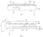
도 8a 및 도 8b를 참조하면, 전자 장치(100)는 전자 장치(100)의 제2 면 (예: -z축을 향하는 면)을 형성하는 제2 커버(180), 전자 장치(100)의 제3 면 (예: 측면)을 형성하는 제1 측면 부재(140), 제2 커버(180)와 제1 측면 부재(140) 사이에 배치되는 리어 케이스(160), 및 제2 커버(180)와 제1 측면 부재(140) 사이에 배치되는 제2 측면 부재(190)를 포함할 수 있다.8A and 8B, the
제2 커버(180)는 중심 부분(181)과 중심 부분(181)을 둘러싸는 테두리 부분(182)을 포함할 수 있다. 제2 커버(180)의 중심 부분(181)에는 전자 장치(100) 내부에 포함된 카메라가 전자 장치(100)의 제2 면으로 보여지도록 투명하게 이루어지는 카메라 영역(1811)이 형성될 수 있다. 제2 커버(180)의 테두리 부분(182)은 제2 측면 부재(190)를 향해 소정의 곡률을 가지고 만곡될 수 있다. The
다양한 실시 예에서, 제2 커버(180)의 중심 부분(181)은 평면으로 이루어질 수 있다. 어떤 실시 예에서, 제2 커버(180)의 중심 부분(181)은 곡면으로 형성될 수 있다.In various embodiments, the
도 8a를 참조하면, 제2 커버(180)의 테두리 부분(182)은 제2 측면 부재(190)의 제3 테두리 부분(1903)과 연결됨으로써, 제2 커버(180) 및 제2 측면 부재(190)가 연결될 수 있다.Referring to FIG. 8A, the
일 실시 예에서, 제2 측면 부재(190)는 리어 케이스(160)를 감싸도록 형성될 수 있다. 제2 측면 부재(190)는 리어 케이스(160)가 배치되는 제1 테두리 부분(1901)과, 제1 테두리 부분(1901)을 둘러싸는 제2 테두리 부분(1902)과, 상기 전자 장치의 외면을 형성하는 제3 테두리 부분(1903)을 포함할 수 있다. In one embodiment, the
도시된 실시 예에서, 리어 케이스(160)는 제2 커버(180)와 인쇄 회로 기판(150) 사이에 배치될 수 있다. 플레이트 부분(142)에는 배터리가 충전될 때, 배터리가 부풀어 오르는 것을 고려한 스웰링 홀이 형성될 수 있다. 스웰링 홀은 배터리의 적어도 일부와 대응되는 영역에 형성될 수 있다. In the illustrated embodiment, the
제2 측면 부재(190)의 제1 테두리 부분(1901) 및 제2 테두리 부분(1902)의 적어도 일부는 제2 커버(180)의 테두리 부분(182)의 곡면과 대응되는 곡면으로 이루어질 수 있다. At least a portion of the
도 8b를 참조하면, 제3 테두리 부분(1903)은 실질적으로 제2 커버(180)의 테두리 부분(182)의 곡면과 동일 곡면 또는 동일 평면으로 형성될 수 있다. 또는 제3 테두리 부분(1903)은 실질적으로 제1 측면 부재(140)의 테두리 부분(141)과 동일 평면 또는 동일 곡면으로 형성될 수 있다. 일례로, 제3 테두리 부분(1903)은 제2 커버(180)의 테두리 부분(182)과 연속적인 곡면으로 이루어질 수 있다. 다양한 실시 예에서, 제2 측면 부재(190)와 제1 측면 부재(140)는 서로 다른 물질로 이루어질 수 있다. 일례로, 제1 측면 부재(140)는 메탈 물질을 포함할 수 있고, 제2 측면 부재(190)는 폴리머 물질을 포함할 수 있다. 이는 제2 측면 부재(190)에 결합 또는 배치된 리어 케이스(160)에 포함된 안테나 모듈(200)의 방사 성능을 유지하기 위한 것으로 상세한 내용은 후술한다.Referring to FIG. 8B, the
리어 케이스(160)는 안테나 모듈(200)이 배치될 수 있는 하나 이상의 안테나 영역을 포함할 수 있다. 이 때, 안테나 영역은 안테나 모듈(200)이 삽입될 수 있는 리세스(161)를 포함할 수 있다. The
일 실시 예에서, 제1 측면 부재(140)는 인쇄 회로 기판(150), 및 배터리(152)가 배치되는 플레이트 부분(142)과 플레이트 부분(142)을 둘러싸는 테두리 부분(141)을 포함할 수 있다. In one embodiment, the
플레이트 부분(142)을 기준으로 전면 방향(예: -z축 방향)에는 디스플레이(예: 도 3의 디스플레이(130))가 배치되고, 후면 방향(예: +z축 방향)에는 인쇄 회로 기판(150), 및 리어 케이스(160)가 순서대로 배치될 수 있다. Based on the
일 실시 예에서, 제1 측면 부재(140)는 제2 측면 부재(190)와 함께 전자 장치(100)의 측면의 상당 부분을 형성할 수 있다. 일례로, 제1 측면 부재(140)의 테두리 부분(141)은 제2 측면 부재(190)의 제3 테두리 부분(1903)과 함께 전자 장치(100)의 외면(예: 측면)의 상당 부분을 형성할 수 있다. 제1 측면 부재(140)의 테두리 부분(141)은 제2 측면 부재(190)의 제3 테두리 부분(1903)과 다른 재질로 이루어질 수 있다. 일례로, 제1 측면 부재(140)의 테두리 부분(141)은 메탈 물질을 포함하되 제2 측면 부재(190)의 제3 테두리 부분(1903)은 폴리머 물질을 포함할 수 있다.In one embodiment, the
도 8b를 참조하면, 제2 커버(180)의 테두리 부분(182), 제2 측면 부재(190)의 제3 테두리 부분(1903)과, 제1 측면 부재(140)의 테두리 부분(141)과, 제1 커버(미도시)(예: 도 3의 전면 플레이트(120))는 함께 전자 장치(100)의 외면(예: 제1 면, 및 제3 면)의 일부를 형성할 수 있다. 제1 측면 부재(140) 및 제2 측면 부재(190)은 제1 커버(예: 도 3의 전면 플레이트(120)), 및 제2 커버(180)(예: 도 3의 후면 플레이트(180)) 사이에 형성될 수 있다.Referring to FIG. 8B, the
도 8b를 참조하면, 제1 커버(120)은 디스플레이(예: 도 3의 디스플레이(130))가 노출될 수 있는 투명 영역(1201)과 상기 투명 영역(1201)의 적어도 일부를 둘러싸는 불투명 영역(1202)(예: 베젤 영역)를 포함할 수 있다. 도시된 실시 예에서, 불투명 영역(1202)은 곡면으로 이루어질 수 있으나 반드시 이에 한정되는 것은 아니며 평면으로 이루어질 수 있다. Referring to FIG. 8B, the
도 8b를 참조하면, <801>은 제1 측면 부재(140)와 제2 측면 부재(190)의 제1 부분(140a, 190a)을 도시하고, <802>는 제1 측면 부재(140)와 제2 측면 부재(190)의 제2 부분(140b, 190b)을 도시한다. Referring to FIG. 8B, <801> shows the
도 8b의 <801>을 참조하면, 제1 측면 부재(140)의 제1 부분(140a)은 제2 부분(140b)에 비해 두께가 두꺼울 수 있다. 도 8b의 <801>을 참조하면, 제2 측면 부재(190)의 제1 부분(190a)는 제2 부분(190b)에 비해 두께가 두꺼울 수 있다.Referring to <801> of FIG. 8B, the
<801>을 참조하면, 제1 측면 부재(140)의 제1 부분(140a)은, 제1 측면 부재(140)의 제1 부분(140a)과 제1 커버(120)가 형성하는 제1 모서리(811)로부터, 제1 측면 부재(140)의 제1 부분(140a)과 제2 측면 부재(190)의 제1 부분(190a)이 형성하는 제2 모서리(812)까지 L1만큼 연장될 수 있다. Referring to <801>, the
<801>을 참조하면, 제2 측면 부재(190)의 제1 부분(190a)은, 상기 제2 모서리(812)로부터 제2 측면 부재(190)의 제1 부분(190a)과 제2 커버(180)가 형성하는 제3 모서리(813)까지 L2만큼 연장될 수 있다.Referring to <801>, the
마찬가지로 <802>을 참조하면, 제1 측면 부재(140)의 제2 부분(140b)은, 제1 측면 부재(140)의 제2 부분(140b)과 제1 커버(120)가 형성하는 제4 모서리(814)로부터, 제1 측면 부재(140)의 제2 부분(140b)과 제2 측면 부재(190)의 제2 부분(190b)이 형성하는 제5 모서리(815)까지 L3만큼 연장될 수 있다.Similarly, referring to <802>, the
<802>을 참조하면, 제2 측면 부재(190)의 제2 부분(190b)은, 상기 제5 모서리(815)로부터 제2 측면 부재(190)의 제2 부분(140b)과 제2 커버(180)이 형성하는 제6 모서리(816)까지 L4만큼 연장될 수 있다. Referring to <802>, the
일 실시 예에서, L1은 L2 보다 길게 형성될 수 있다. L3는 L4 보다 길게 형성될 수 있다.In one embodiment, L1 may be formed longer than L2. L3 may be formed longer than L4.
일 실시 예에서, 제1 측면 부재(140)는 제1 부분(140a)의 두께(예: L1)가 제2 부분(140b)의 두께(예: L3)보다 크게 형성될 수 있다. 일 실시 예에서, 제2 측면 부재(190)의 제1 부분(190a)의 두께(예: L2)는 제2 부분(190b)의 두께(예: L4)보다 크게 형성될 수 있다.In one embodiment, the
도 8b에 도시된 실시 예에서, 전자 장치의 제3 면을 형성하는 제1 측면 부재(140)는 제1 측면 부재(140)의 테두리 부분(도 8a의 테두리 부분(141))을 포함할 수 있다. 전자 장치의 제3 면을 형성하는 제2 측면 부재(190)는 제2 측면 부재(190)의 제3 테두리 부분(도 8a의 제3 테두리 부분(1903))을 포함할 수 있다.In the embodiment illustrated in FIG. 8B, the
도 9a는 일 실시 예에 따른 전자 장치의 안테나 모듈의 사시도이다. 도 9b는 일 실시 예에서, 도 9a에 도시된 안테나 모듈의 안테나 기판의 내부를 도시한 도면이다.9A is a perspective view of an antenna module of an electronic device according to an embodiment. 9B is a diagram illustrating the interior of an antenna substrate of the antenna module shown in FIG. 9A in one embodiment.
도 9a 및 도 9b를 참조하면, 일 실시 예에 따른 전자 장치(100)의 안테나 모듈(200)은 안테나 기판(2001), RFIC 모듈(2002), 및 케이블(216)을 포함할 수 있다. 9A and 9B, the
도 9a를 참조하면, 안테나 기판(2001)은 제1 RF 신호를 방사하는 방사 영역(2111)이 형성된 제1 면(211), 상기 제1 면(211)과 마주보는 제2 면(212), 및 상기 제1 면(211)과 상기 제2 면(212) 사이에 형성된 제3 면(213)을 포함할 수 있다. 제1 면(211)에는 방사 영역(2111)이 형성될 수 있다. Referring to FIG. 9A, the
방사 영역(2111)은 안테나 기판(2001)의 제1 면(211)에 형성되는 도전성 패턴에 의해 형성되거나, 또는 도 9b에 도시된 바와 같이 안테나 기판(2001)에 포함된 복수의 층 중 일부에 형성된 도전성 패턴(예: 제1 안테나 엘리먼트(214))에 의해 형성될 수 있다.The
도시된 실시 예에서, 제2 면(212)에는 RFIC 모듈(2002)(예: 도 5의 RFIC 모듈(590))이 배치될 수 있다. 이 때, RFIC 모듈(2002)은 RFIC(예: 도 4의 RFIC(526)), RFIC로부터 발생되는 발열의 쿨링을 위한 방열 부재, 및 전자파 차단을 위한 차폐 부재를 포함할 수 있다. 제2 면(212)에는 케이블(216)이 결합되는 대응 커넥터(217)가 형성될 수 있다. In the illustrated embodiment, the RFIC module 2002 (eg, the RFIC module 590 of FIG. 5) may be disposed on the
도 9b를 참조하면, 안테나 기판(2001)은 복수의 층을 포함할 수 있다. 안테나 기판(2001)의 제3 면(213)은 제2 안테나 엘리먼트(215)가 연장된 제3-1 면(2131), 상기 제3-1 면(2131)에 마주보는 제3-2 면(2132), 및 상기 제3-1 면(2131)과 상기 제3-2 면(2132)을 연결하는 제3-3 면(2133)을 포함할 수 있다. Referring to FIG. 9B, the
복수의 층에는 제1 안테나 엘리먼트(214), 및 제2 안테나 엘리먼트(215)가 형성될 수 있다. 제1 안테나 엘리먼트(214)는 도 9a에 도시된 방사 영역(2111)을 형성할 수 있다. 이 때, 제1 안테나 엘리먼트(214)는 안테나 모듈(200)의 제1 면(211)에 형성되거나, 복수의 층들 중 일부 층의 지정된 영역에 형성될 수 있다. 이 때, 지정된 영역은 도 9a의 제1 면(211)에 형성된 방사 영역(2111)에 대응되는 영역일 수 있다.The
일 실시 예에서, 제2 안테나 엘리먼트(215)는 복수의 층 중 적어도 하나의 층에 형성될 수 있다. 제2 안테나 엘리먼트(215)는 제3 면들(2131, 2132, 2133) 중 적어도 하나를 향하는 방향으로 연장될 수 있으며, 제2 안테나 엘리먼트(215)에 의해 제2 RF신호가 방사될 수 있다. 다양한 실시 예에서, 제2 안테나 엘리먼트(215)는 제1 안테나 엘리먼트(214)와 동일한 층에 형성될 수 있다.In one embodiment, the
어떤 실시 예에서, 제1 RF 신호를 방사하기 위한 제1 안테나 엘리먼트(214)가 형성하는 영역을 제1 방사 영역(예: 도 9a의 방사 영역(2111))으로 지칭할 수 있다. 또한, 제2 RF 신호를 방사하기 위한 제2 안테나 엘리먼트(215)가 형성하는 영역을 제2 방사 영역으로 지칭할 수 있다. 제2 방사 영역은 제2 안테나 엘리먼트(215)가 향하는 면(예: 도 9b의 3-1면(2131)) 또는 제2 RF 신호가 방사되는 면을 포함할 수 있다.In some embodiments, an area formed by the
도시된 실시 예에서, 제2 방사 영역, 또는 제2 안테나 엘리먼트(215)가 연장된 제3-1 면(2131)은 ① 방향을 향할 수 있다. 여기서 ① 방향은 후술하는 바와 같이 하우징 구조물의 외측을 향하는 방향일 수 있다. In the illustrated embodiment, the second radiation region, or the 3-1
다양한 실시 예에서, 제2 안테나 엘리먼트(215)는 다이폴 안테나를 형성할 수 있다.In various embodiments, the
다양한 실시 예에서, 안테나 모듈(200)은 제1 면(211)을 통해 제1 RF 신호를 방사하고, 제3-1 면(2131)을 통해 제2 RF 신호를 방사할 수 있다. In various embodiments, the
도 10는 일 실시 예에 따른 전자 장치(100)의 안테나 모듈(200)의 배치도이다. 10 is a layout view of the
도 10을 참조하면, 전자 장치(100)는 리어 케이스(160)에 배치되는 하나 이상의 안테나 모듈(310, 320, 330)을 포함할 수 있다. 안테나 모듈(310, 320, 330)은 전자 장치(100)의 후면을 도시한 도 10를 기준으로 상부에 배치된 제1 안테나 모듈(310), 좌측부에 배치된 제2 안테나 모듈(320), 및 우측부에 배치된 제3 안테나 모듈(330)을 포함할 수 있다. 상기 안테나 모듈들(310, 320, 330)은 리어 케이스(160)의 후면(예: 제2 커버를 향하는 방향)을 향하는 면에 배치될 수 있다. 여기서, 안테나 모듈들(310, 320, 330)은, 제1 면(예: 도 9a 및 도 9b에 도시된 제1 면(211))이 전자 장치의 제2 면(예: 도 3의 제2 커버(180)가 형성하는 면)을 향하도록 리어 케이스(160)에 배치될 수 있다.Referring to FIG. 10, the
다양한 실시 예에서, 제1 안테나 모듈(310)은 제1 측면 부재(140)의 제1 부분(140a) 및/또는 제2 측면 부재(190)의 제1 부분(190a)에 인접하게 배치될 수 있다. 제2 안테나 모듈(320), 및 제3 안테나 모듈(330)은 제1 측면 부재(140)의 제2 부분(140b) 및/또는 제2 측면 부재(190)의 제2 부분(190b)에 인접하게 배치될 수 있다. In various embodiments, the
일 실시 예에서, 리어 케이스(160)의 안테나 모듈들(310, 320, 330)이 배치된 면에는, 상기 안테나 모듈들(310, 320, 330)을 덮도록 제2 커버(예: 도 8a의 제2 커버(180))가 배치될 수 있다. 리어 케이스(160)의 가장자리 일부는 전자 장치(100)의 후면을 볼 때, 제2 측면 부재(190)의 제1 테두리 부분(1901), 및 제2 테두리 부분(1902)에 의해 가려질 수 있다. In one embodiment, on the surface of the
도 11는 일 실시 예에 따른 전자 장치(100)의 제1 안테나 모듈(310)이 배치된 단면도이다.11 is a cross-sectional view of the
일 실시 예에서, 전자 장치(100)는 전자 장치(100)의 제2 면(예: 후면)을 형성하는 제2 커버(180), 전자 장치(100)의 제1 면(예: 전면)을 형성하는 제1 커버(120), 및 전자 장치(100)의 제3 면(예: 측면)을 형성하는 제1 측면 부재(140) 및 제2 측면 부재(190)를 포함할 수 있다. In one embodiment, the
일 실시 예에서, 전자 장치(100)는 제1 커버(120), 제2 커버(180), 제1 측면 부재(140), 및 제2 측면 부재(190)에 의해 형성되는 내부 공간을 포함할 수 있다. 상기 내부 공간에는 하나 이상의 인쇄 회로 기판(150), 디스플레이(130), 또는 리어 케이스(160)가 배치될 수 있다. In one embodiment, the
일 실시 예에서, 디스플레이(130)는 제1 커버(120)를 향하도록 제1 커버(120) 아래에 배치될 수 있다. 인쇄 회로 기판(150)은 디스플레이(130) 아래에 배치되거나, 또는 리어 케이스(160)의 제1 커버(120)를 향하는 면(예: 도면을 기준으로 하부면)에 배치될 수 있다. 리어 케이스(160)에는 제1 안테나 모듈(310)이 배치되는 리세스(161)가 형성될 수 있다.In one embodiment, the
일 실시 예에서, 제1 안테나 모듈(310)은 제1 면(311)(예: 도 9b의 제1 면(211)), 제1 면(311)에 마주보며 RFIC 모듈(3102)(예: 도 9a의 RFIC 모듈(2002))이 배치되는 제2 면(312), 및 상기 제1 면(311)과 제2 면(312) 사이에 형성되는 제3 면(3131, 3132)(예: 도 9b의 제3 면(2131, 2132)) 포함할 수 있다. 이 때, 제1 면(311)에는 제1 RF 신호가 방사되는 제1 방사 영역(3111)(예: 도 9b의 제1 방사 영역(2111))이 형성되고, 제3 면(3131, 3132)의 적어도 일부에는 제2 RF신호가 방사되는 제2 방사 영역(예: 제3-1 면(3131))(예: 도 9b의 제3-1 면(2131))이 형성될 수 있다. 제2 방사 영역은 제3-1 면(3131)에 포함될 수 있다. In one embodiment, the
일 실시 예에서, 제1 안테나 모듈(310)은, 상기 제1 방사 영역(3111)이 제2 커버(180)를 향하고, 및 상기 제2 방사 영역(예: 제3-1 면(3131))이 제2 측면 부재(190)를 향하도록, 상기 리어 케이스(160)에 형성된 리세스(161)에 배치될 수 있다. 일례로, 제1 안테나 모듈(310)은 제1 면(311)이 제2 커버(180)와 소정의 각도를 이루도록 마주보고, 및 제3-1 면(3131)이 전자 장치(100)의 외측을 향하도록 배치될 수 있다. 일례로, 제1 안테나 모듈(310)은 제3-1 면(3131)에 형성된 제2 방사 영역으로부터 방사되는 제2 RF 신호의 방사 범위(도면에서 점선으로 표시된 범위)가 제1 측면 부재(140)에 의해 가리지 않도록, 제2 커버(180)에 대해 소정의 각도로 기울어져 배치될 수 있다. In one embodiment, the
다양한 실시 예에서, 제2 커버(180)와 제1 안테나 모듈(310)은 소정의 간격으로 이격될 수 있다. 제1 안테나 모듈(310)의 제1 면(311)과 제2 커버(180) 사이의 간격은 전자 장치(100)의 내측으로부터 전자 장치(100)의 외측으로 갈수록 작아질 수 있다. In various embodiments, the
도 11를 참조하면, 제1 안테나 모듈(310)의 제1 면(311) 중 상기 방사면에 대향하는 면(예: 제3-2 면(3132))에 인접한 제1 영역은 제2 커버(180)와 제1 간격(d1)만큼 이격되고, 제1 안테나 모듈(310)의 제1 면(311) 중 제2 RF 신호가 방사되는 방사면(예: 제3-1 면(3131))과 인접한 제2 영역은 제2 커버(180)와 제2 간격(d2)만큼 이격될 수 있다. Referring to FIG. 11, a first area adjacent to a surface (eg, 3-2 surface 3132) facing the radiation surface of the
이 때, 제1 간격(d1)은 제2 간격(d2)보다 크게 형성될 수 있다. 즉, 방사면(예: 제3-1 면(3131))이 측면 부재(예: 제1 측면 부재(140), 제2 측면 부재(190))의 일부, 및 제2 커버(180)의 일부와 마주보도록 제2 커버(180) 측으로 기울어져 배치될 수 있다. 이로써, 제2 RF 신호는제2 측면 부재(190) 및 제2 커버(180)를 통과하도록, 제2 RF 신호의 방사 범위가 형성될 수 있다.At this time, the first gap d1 may be formed larger than the second gap d2. That is, the radiation surface (eg, the 3-1 surface 3131) is a part of the side member (eg, the
다양한 실시 예에서, 제1 안테나 모듈(310)은 제1 방사 영역(3111)이 전자 장치(100)의 제2 면(예: 제2 커버(180)가 형성하는 면)을 향하고, 제2 방사 영역(예: 제3-1 면(3131))이 전자 장치(100)의 제3 면(예: 제1 측면 부재(140)와 제2 측면 부재(190)가 형성하는 면)을 향하도록 리어 케이스(160)에 배치될 수 있다.In various embodiments, the
도시된 실시 예에서, 제1 안테나 모듈(310)은 제2 커버(180)에 대해 소정의 각도로 배치될 수 있다. 이 때, 제1 안테나 모듈(310)과 제2 커버(180)의 각도는, 제1 안테나 모듈(310)의 제1 면(311)이 향하는 방향(예: 제1 면(311)의 법선 벡터)과 제2 커버(180)(예: 제2 커버(180)의 법선 벡터)가 향하는 방향이 이루는 각도일 수 있다. 일례로, 상기 소정의 각도는 0도 내지 15도일 수 있다.도시된 실시 예에서, 제1 안테나 모듈(310)의 제1 면(311)은 제2 방사 영역이 형성된 제3-1 면(3131)과 수직하게 연결될 수 있다. 따라서, 제1 안테나 모듈(310)의 제3-1 면(3131)은 제2 커버(180)의 법선 벡터에 수직한 방향(예: ① 방향)에 대해 상기 소정의 각도만큼 제2 커버(180)를 향해 기울어져 배치될 수 있다.In the illustrated embodiment, the
다양한 실시 예에서, 제2 커버(180)는 평면 부분과 평면 부분을 둘러싸는 곡면 부분을 포함할 수 있다. 이 때, 제1 안테나 모듈(310)과 제2 커버(180)가 이루는 각도는 제2 커버(180)의 평면 부분의 법선 벡터와 제1 안테나 모듈(310)의 제1 면(311)의 법선 벡터가 이루는 각도일 수 있다.In various embodiments, the
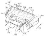
도 12a, 도 12b, 및 도 12c는 일 실시 예에 따른 전자 장치(100)의 제1 안테나 모듈(310)과 제1 안테나 모듈(310)이 배치된 리어 케이스(160)를 도시한 도면이다.12A, 12B, and 12C are views illustrating a
도 12a를 참조하면, 리어 케이스(160)에 형성된 리세스(161)에는 제1 안테나 모듈(310)을 고정하기 위한 돌출부(162)가 형성될 수 있다. Referring to FIG. 12A, a
돌출부(162)는 리세스(161)의 내측면으로부터 리세스(161)의 내측으로 돌출 형성될 수 있다. 돌출부(162)는 제1 안테나 모듈(310)의 제1 면(311)을 가압함으로써, 제1 안테나 모듈(310)이 제2 커버(180) 방향으로 이탈되는 것을 방지할 수 있다.The
도 12b를 참조하면, 상기 리세스(161)의 내측면 중 제1 안테나 모듈(310)의 제2 면(312)과 마주보는 면은, 제1 안테나 모듈(310)의 배치 각도와 대응되는 각도를 가지는 경사면(164)으로 이루어질 수 있다. 상기 경사면(164)에는 제1 안테나 모듈(310)의 제2 면(312)에 배치된 RFIC 모듈(3102)이 삽입될 수 있는 추가 리세스(165)가 형성될 수 있다. Referring to FIG. 12B, a surface facing the
다양한 실시 예에서, 제1 안테나 모듈(310)은 제2 면(312)이 리세스(161)의 경사면(164)에 의해 지지되며, 리세스(161)의 내측면에 형성된 돌출부(162)에 의해 리세스(161) 내부에 압입될 수 있다. In various embodiments, the
도 12c를 참조하면, 다양한 실시 예에서 전자 장치(100)는 제1 안테나 모듈(310)을 리어 케이스(160)의 리세스(161)에 고정하기 위해 제1 안테나 모듈(310)을 덮는 덮개 부재(166)를 포함할 수 있다. 덮개 부재(166)는 비 금속성 물질로 이루어져 제1 면(311)으로부터 방사되는 제1 RF 신호에 영향을 미치지 않을 수 있다. 상기 덮개 부재(166)는 제2 커버(180)에 의해 리세스(161) 내부에 고정되거나 고정을 위한 별도의 구성을 가질 수 있다.Referring to FIG. 12C, in various embodiments, the
제1 안테나 모듈(310)은 제1 면(311)과 제2 면(312)을 포함하는 안테나 기판(3101), 안테나 기판(3101)의 제2 면(312)에 배치되는 RFIC 모듈(3102), 안테나 기판의 제2 면(312)에 형성되는 커넥터(317), 및 상기 커넥터(317)와 연결되는 FPCB(flexible printed circuit board)(316)를 포함할 수 있다. 도시된 실시 예에서, RFIC 모듈(3102)은 경사면(164)에 배치될 수 있다. 안테나 기판(3101)에 형성된 커넥터(317)는 RFIC 모듈(3102)에 비해 경사면(164)을 향해 더 돌출될 수 있다. 따라서, 안테나 모듈(310)이 수용되는 리세스(161)에는 커넥터(317) 및 FPCB(316)의 일부를 수용하기 위한 추가 리세스(165)가 형성될 수 있다. 추가 리세스(165)는 경사면(164)에 형성될 수 있다.The
도 13a는 일 실시 예에 따른 전자 장치(100)의 제2 안테나 모듈(320)의 배치가 도시된 단면도이다. 도 13b는 일 실시 예에 따른 전자 장치(100)의 제3 안테나 모듈(330)의 배치가 도시된 단면도이다. 13A is a cross-sectional view illustrating an arrangement of the
도 13a를 참조하면, 제2 안테나 모듈(320)은 리어 케이스(160)의 양 측부(예: 도 8b의 x축 방향 양 단부)에 배치될 수 있다. 13A, the
도시된 실시 예에 따른 전자 장치(100)는, 제1 커버(120), 제1 커버(120)와 대향하는 제2 커버(180), 제1 커버(120)에 연결되며 전자 장치(100)의 외면(예: 측면)의 일부를 형성하는 테두리 부분(141)와 상기 테두리 부분(141)로부터 제1 커버(120)와 제2 커버(180) 사이로 연장되는 플레이트 부분(142)를 포함하는 제1 측면 부재(140), 및 제2 커버(180)와 제1 측면 부재(140)를 연결하며 전자 장치(100)의 외면(예: 측면)의 나머지 일부를 형성하는 제2 측면 부재(190)을 포함할 수 있다.The
다양한 실시 예에서, 전자 장치(100)는 제1 측면 부재(140)의 플레이트 부분(142)와 제2 커버(180) 사이에 배치되는 인쇄 회로 기판(150), 인쇄 회로 기판(150)과 제2 커버(180) 사이에 배치되는 리어 케이스(160), 및 플레이트 부분(142)를 중심으로 인쇄 회로 기판(150)과 반대 방향(예: 리어 케이스(160)의 제1 커버(120)를 향하는 면)에 배치되는 디스플레이(130)를 더 포함할 수 있다.In various embodiments, the
어떤 실시 예에서, 전자 장치(100)는 제1 커버(120), 제2 커버(180), 및 제1 커버(120)와 제2 커버(180) 사이의 공간을 둘러싸는 제1 측면 부재(140)를 포함하는 하우징(예: 도 1의 하우징(110))을 포함할 수 있으며, 하우징 내부에는 제1 커버(120)로부터 제2 커버(180)를 향하는 방향을 따라 순서대로 디스플레이(130), 인쇄 회로 기판(150), 및 리어 케이스(160)가 배치될 수 있다.In some embodiments, the
도시된 실시 예에서, 리어 케이스(160)에는 제2 안테나 모듈(320)이 배치될 수 있다. 제2 안테나 모듈(320)은 제1 면(321)(예: 도 9b의 제1 면(211)), 제1 면(321)에 마주보며 RFIC 모듈(3202)(예: 도 9a의 RFIC 모듈(2002))이 배치되는 제2 면(322)(예: 도 9b의 제2 면(212)), 및 상기 제1 면(321)과 제2 면(322) 사이에 형성되는 제3 면(3231, 3232)(예: 도 9b의 제3 면(2131, 2132))을 포함하는 안테나 기판(3201), 및 상기 제2 면(322)에 배치되는 RFIC 모듈(3202)를 포함할 수 있다. In the illustrated embodiment, the
이 때, 안테나 기판(3201)의 제1 면(321)에는 제1 RF 신호가 방사되는 제1 방사 영역(3211)(예: 도 9a의 제1 방사 영역(2111))이 형성되고, 제3 면(3231, 3232)의 적어도 일부(예: 제3-1 면(3231))에는 제2 RF신호가 방사되는 제2 방사 영역(예: 도 9b의 제3-1 면(2131))이 형성될 수 있다.At this time, a first radiation region 3211 (for example, the
일 실시 예에서, 제2 안테나 모듈(320)은, 상기 제1 방사 영역(3211)이 제2 커버(180)를 향하고, 및 상기 제3-1 면(3231)이 제2 측면 부재(190)를 향하도록, 상기 리어 케이스(160)에 배치될 수 있다. 일 실시 예에서, 제2 안테나 모듈(320)은 제1 안테나 모듈(예: 도 11의 제1 안테나 모듈(310))과 달리 제2 커버(180)(예: 도 11의 제2 커버(180))와 나란하게 배치될 수 있다. In one embodiment, the
도 13b를 참조하면, 제3 안테나 모듈(330)은 리어 케이스(160)의 양 측부(예: 도 8b의 x축 방향 양 단부)에 배치될 수 있다. 13B, the
도시된 실시 예에서, 리어 케이스(160)에는 제3 안테나 모듈(330)이 배치될 수 있다. 제3 안테나 모듈(330)은 제1 면(331)(예: 도 9b의 제1 면(211)), 제1 면(331)과 마주보는 제2 면(332)(예: 도 9b의 제2 면(212)), 및 상기 제1 면(331)과 제2 면(332) 사이에 형성되는 제3 면(3331, 3332)(예: 도 9b의 제3 면(2131, 2132))을 포함하는 안테나 기판(3301), 및 상기 제2 면(332)에 배치되는 RFIC 모듈(3302)(예: 도 9a의 RFIC 모듈(2002))를 포함할 수 있다. In the illustrated embodiment, the
이 때, 안테나 기판(3301)의 제1 면(331)에는 제1 RF 신호가 방사되는 제1 방사 영역(3311)(예: 도 9a의 제1 방사 영역(2111))이 형성되고, 제3 면(3331, 3332)의 적어도 일부(예: 제3-1 면(3331))에는 제2 RF신호가 방사되는 제2 방사 영역(예: 도 9b의 제3-1 면(2131))이 형성될 수 있다.At this time, a first radiation region 3311 (for example, a
일 실시 예에서, 제3 안테나 모듈(330)은, 상기 제1 방사 영역(3311)이 제2 커버(180)를 향하고, 및 제2 방사 영역이 형성된 상기 제3-1 면(3331)이 제2 측면 부재(190)를 향하도록, 상기 리어 케이스(160)에 배치될 수 있다. 일 실시 예에서, 제3 안테나 모듈(330)은 제1 안테나 모듈(예: 도 11의 제1 안테나 모듈(310))과 달리 제2 커버(180)(예: 도 11의 제2 커버(180))와 나란하게 배치될 수 있다. In one embodiment, the
다양한 실시 예에서, 도 13a에 도시된 제2 안테나 모듈(320) 및 도 13b에 도시된 제3 안테나 모듈(330)은 제2 커버(180)와 나란하게 배치된 것으로 도시되나, 반드시 이에 한정되는 것은 아니며 제2 안테나 모듈(320) 및/또는 제3 안테나 모듈(330)은 제2 커버(180)와 소정의 각도를 이루도록 기울어져 배치될 수 있다. 이 때, 소정의 각도는 제1 안테나 모듈(예: 도 11의 제1 안테나 모듈(310))과 제2 커버(180)가 이루는 각도보다 작을 수 있다.In various embodiments, the
도 11, 도 13a, 및 도 13b를 참조하면, 본 문서에서 설명되는 제1 안테나 모듈(예: 도 11의 제1 안테나 모듈(310)), 제2 안테나 모듈(예: 도 13a의 제2 안테나 모듈(320)), 및 제3 안테나 모듈(예: 도 13b의 제3 안테나 모듈(330))의 배치 각도는, 하우징 또는 전자 장치(100)의 외관을 이루는 구조들의 재질에 따라 달라질 수 있다. 일례로, 상기 배치 각도는 RF 신호(예: 다이폴 안테나로부터 방사되는 신호)가 방사되는 범위에 포함되는 하우징 구조들의 재질에 따라 결정될 수 있다. 11, 13A, and 13B, a first antenna module (eg, the
예를 들어, 전자 장치(100) 또는 하우징의 측면을 형성하는 측면 부재(예: 제1 측면 부재(140), 제2 측면 부재(190))들이 전파 방사에 영향을 주지 않는 물질(예: 세라믹, 폴리머 등)로만 이루어진 경우, 제1 안테나 모듈(310), 제2 안테나 모듈(320), 및 제3 안테나 모듈(330) 각각에 포함된 안테나 기판(3101, 3201, 3301)의 제1 면(311, 321, 331)이 제2 커버(180)와 나란하게 배치될 수 있다. 즉, 제2 RF 신호가 방사되는 제2 방사 영역(예: 제3-1 면(3131, 3231, 3331))이 상기 측면 부재(예: 제1 측면 부재(140), 제2 측면 부재(190)들을 향해 배치될 수 있다. For example, a side member (eg,
예를 들어, 전자 장치(100) 또는 하우징의 측면을 형성하는 측면 부재들(예: 제1 측면 부재(140), 제2 측면 부재(190)) 중 일부가 전파 방사에 영향을 줄 수 있는 물질(예: 메탈)을 포함하고, 나머지 일부가 전파 방사에 영향을 주지 않는 물질(예: 세라믹, 폴리머 등)을 포함하는 경우(예: 제1 측면 부재(140)가 메탈로 이루어지고, 제2 측면 부재(190)가 폴리카보네이트로 이루어진 경우), 제1 안테나 모듈(310), 제2 안테나 모듈(320), 및 제3 안테나 모듈(330)은, 각각에 포함된 안테나 기판(3101, 3201, 3301)의 제1 면(311, 321, 331)이 제2 커버(180)와 소정의 각도를 형성하도록 배치될 수 있다. 즉, 제2 RF 신호가 방사되는 제2 방사 영역(예: 제3-1 면(3131, 3231, 3331))이 상기 측면 부재들(140, 190) 중 전파 방사에 영향을 주지 않는 물질을 포함하는 부분을 향해 배치(예: 폴리카보네이트로 이루어진 제2 측면 부재(190)를 향해 배치)될 수 있다. 안테나 모듈(310, 320, 330)은 제2 RF 신호의 방사 범위에 메탈 물질, 또는 메탈 물질로 이루어진 구조물(예: 제1 측면 부재(140))이 포함되지 않도록 배치될 수 있다. For example, some of the side members (eg, the
다양한 실시 예에서, 전자 장치(100))는 제1 방향으로 향하는 전면 플레이트(120), 상기 제1 방향의 반대 방향인 제2 방향으로 향하는 후면 플레이트(180), 및 상기 전면 플레이트(120)와 상기 후면 플레이트(180) 사이의 공간을 둘러싸고, 적어도 일부분이 금속 물질로 형성된 측면 부재(예: 도 11의 제1 측면 부재(140), 및 제2 측면 부재(190)를 포함함)를 포함하는 하우징; 상기 전면 플레이트(120)를 통해 보여지는 디스플레이(130); 및 상기 공간 내에 위치하는 안테나 모듈(예: 도 11의 제1 안테나 모듈(310))로서, 상기 제1 방향 및 상기 제2 방향과는 다른 제3 방향으로 향하는 제1 면(311), 상기 제3 방향과 반대인 제4 방향으로 향하는 제2 면(312), 및 상기 제1 면(311) 및 상기 제2 면(312) 사이에, 상기 측면 부재(140, 190)에 인접하여, 상기 제3 방향 및 상기 제4 방향과 수직이며 상기 측면 부재(140, 190)의 제1 부분(예: 도 11의 제2 측면 부재(190)) 쪽으로 향하는 제5 방향으로 연장된 적어도 하나 이상의 도전성 엘리먼트(예: 도 12a의 제2 안테나 엘리먼트(315))를 포함하는 안테나 모듈 (310)을 포함하며, 상기 제1 면(311)은, 상기 측면 부재(140, 190)의 제1 부분(190)으로부터 가장 가까운 제1 가장자리(a first periphery)(예: 도 11의 D2가 도시된 부분), 및 상기 측면 부재(140, 190)의 제1 부분(190)으로부터 가장 먼 제2 가장자리(예: 도 11의 D1이 도시된 부분)를 포함하며, 상기 제1 가장자리가 상기 제2 가장자리보다 상기 후면 플레이트(180)와 더 가깝도록, 상기 제1 면(311)이 상기 후면 플레이트(180)와 1도 내지 15도 사이의 각을 형성할 수 있다.In various embodiments, the electronic device 100 includes a front plate 120 facing in a first direction, a back plate 180 facing in a second direction opposite to the first direction, and the front plate 120 Surrounding the space between the rear plates 180, including at least a portion of a side member formed of a metal material (for example, including the first side member 140 and the second side member 190 of FIG. 11) housing; A display 130 shown through the front plate 120; And an antenna module (eg, the first antenna module 310 of FIG. 11) located in the space, the first surface 311 facing the third direction different from the first direction and the second direction, and the first The second surface 312 facing the fourth direction opposite to the three directions, and between the first surface 311 and the second surface 312, adjacent to the side members 140 and 190, the first At least one conductive element (3) and at least one conductive element perpendicular to the fourth direction and extending in a fifth direction toward the first portion of the side members 140, 190 (eg, the second side member 190 of FIG. 11) Example: It includes an antenna module 310 including the second antenna element 315 of Figure 12a, the first surface 311 is from the first portion 190 of the side member (140, 190) A first periphery (for example, a portion in which D2 in FIG. 11 is shown), and a second farthest from the first portion 190 of the side members 140 and 190 An edge (for example, a portion in which D1 in FIG. 11 is shown) includes the first surface 311 so that the first surface 311 is closer to the rear plate 180 than the second edge. 180) and between 1 and 15 degrees.
다양한 실시 예에서, 20 GHz 내지 100 GHz 사이의 주파수를 가진 신호를 송신 및/또는 수신하도록 구성된 무선 통신 회로(예: 도 11의 RFIC 모듈(3102))를 더 포함하며, 상기 도전성 엘리먼트(예: 도 12a의 제2 안테나 엘리먼트(315))는 상기 무선 통신 회로(3102)와 전기적으로 연결될 수 있다.In various embodiments, a wireless communication circuit configured to transmit and / or receive a signal having a frequency between 20 GHz and 100 GHz (eg, the
다양한 실시 예에서, 상기 도전성 엘리먼트(315)는 다이폴 안테나를 형성할 수 있다. In various embodiments, the
다양한 실시 예에서, 상기 후면 플레이트(180)는, 상기 측면 부재(140, 190)의 제1 부분(190)에 인접하면서, 구부러진 표면을 형성하는 엣지 부분을 더 포함할 수 있다.In various embodiments, the
다양한 실시 예에서, 상기 측면 부재(140, 190)의 제1 부분(190)은 비도전성 물질을 포함할 수 있다.In various embodiments, the
다양한 실시 예에서, 상기 디스플레이(130)와 상기 후면 플레이트(180) 사이에 위치한 미드 플레이트(예: 도 11의 리어 케이스(160), 또는 도 3의 제1 지지 부재(142))를 더 포함하며, 상기 안테나 모듈 (310)은 상기 미드 플레이트(160) 및 상기 후면 플레이트(180) 사이에 배치될 수 있다.In various embodiments, a mid plate (eg, the
다양한 실시 예에서, 상기 미드 플레이트(160)는 상기 제1 방향을 향하되 상기 디스플레이(130)를 향하는 제1 면, 및 상기 제1 면에 대향하며 상기 안테나 모듈(310)이 배치되는 제2 면을 포함하고, 상기 미드 플레이트(160)의 상기 제2 면에는 상기 안테나 모듈(310)이 배치되는 리세스(161)가 형성되고, 상기 리세스(161)는, 상기 안테나 모듈(310)의 상기 제2 면(312)이 배치되며, 상기 안테나 모듈(310)의 상기 제1 면(311)이 상기 후면 플레이트(180)와 형성하는 각도와 대응되는 각도를 가지는 경사면(164)을 포함할 수 있다.In various embodiments, the
다양한 실시 예에서, 상기 측면 부재(140, 190)는 상기 전면 플레이트(120)와 상기 후면 플레이트(180) 사이의 상기 전자 장치(100)의 측면을 형성하며, 제1 길이를 갖는 단변부(예: 도 10의 단변부(140a)), 및 상기 제1 길이보다 긴 제2 길이를 갖는 장변부(예: 도 10의 장변부(140b))를 포함하고, 상기 단변부(140a)는 상기 전면 플레이트(120)로부터 상기 후면 플레이트(180)까지 제1 높이로 형성되고, 상기 장변부(140b)는 상기 전면 플레이트(120)로부터 상기 후면 플레이트(180)까지 상기 제1 높이보다 높은 제2 높이로 형성될 수 있다.In various embodiments, the
다양한 실시 예에서, 상기 안테나 모듈(예: 제1 안테나 모듈(310), 제2 안테나 모듈(320), 및 제3 안테나 모듈(330)을 포함함)은 상기 단변부(140a)와 인접하게 배치되는 제1 안테나 모듈(예: 제1 안테나 모듈(310)), 및 상기 장변부(140b)와 인접하게 배치되는 제2 안테나 모듈(예: 제2 안테나 모듈(320) 및 제3 안테나 모듈(330))을 포함하고, 상기 제1 안테나 모듈(310)의 상기 제1 면(311)이 상기 후면 플레이트(180)와 이루는 각도는, 상기 제2 안테나 모듈(320, 330)의 상기 제1 면(321, 331)이 상기 후면 플레이트(180)와 이루는 각도보다 클 수 있다.In various embodiments, the antenna module (eg, including the
다양한 실시 예에서, 전자 장치(100)는 제1 방향으로 향하는 전면 플레이트(120), 상기 제1 방향의 반대 방향인 제2 방향으로 향하는 평면 부분과 상기 평면 부분을 둘러싸는 곡면 부분을 포함하는 후면 플레이트(180), 및 상기 전면 플레이트(120)와 상기 후면 플레이트(180) 사이의 공간을 감싸고, 적어도 일부분이 금속 물질로 형성된 측면 부재(예: 도 11의 제1 측면 부재(140), 및 제2 측면 부재(190)를 포함함)를 포함하는 하우징; 상기 전면 플레이트(120)를 통해 보여지는 디스플레이(130); 및 상기 공간 내에 위치하는 안테나 모듈(310)로서, 상기 제1 방향 및 상기 제2 방향과는 다른 제3 방향으로 향하는 제1 면(311), 상기 제3 방향과 반대인 제4 방향으로 향하는 제2 면(312), 및 상기 제1 면(311) 및 상기 제2 면(312) 사이에, 상기 측면 부재(140, 190)에 인접하여, 상기 제3 방향 및 상기 제4 방향과 수직이며 상기 측면 부재(140, 190)의 제1 부분(예: 도 11의 제2 측면 부재(190))을 향하는 제5 방향으로 연장된 적어도 하나 이상의 도전성 엘리먼트(예: 도 12a의 제2 안테나 엘리먼트(315))를 포함하는 안테나 모듈(310)을 포함하며, 상기 제1 면(311)은, 상기 측면 부재(140, 190)의 상기 제1 부분(190)으로부터 가장 가까운 제1 가장자리(a first periphery), 및 상기 측면 부재(140, 190)의 상기 제1 부분(190)으로부터 가장 먼 제2 가장자리를 포함하며, 상기 제1 가장자리가 상기 제2 가장자리보다 상기 후면 플레이트(180)와 더 가깝도록, 배치될 수 있다. In various embodiments, the
다양한 실시 예에서, 상기 측면 부재(140, 190)는 제1 길이를 갖는 단변부(140a), 및 상기 제1 길이보다 긴 제2 길이를 갖는 장변부(140b)를 포함하며, 상기 전면 플레이트(120)와 상기 후면 플레이트(180) 사이의 상기 전자 장치(100)의 측면을 형성하고, 상기 측면 부재(140, 190)는 금속 물질로 형성되는 금속 부분(예: 도 11의 제1 측면 부재(140)) 및 비금속 물질로 형성되는 비금속 부분(예: 도 11의 제2 측면 부재(190))을 포함하고, 상기 전자 장치의 상기 전면 플레이트(120)를 위에서 볼 때, 상기 단변부(140a)에 포함된 상기 비금속 부분(190)은 상기 장변부(140b)에 포함된 상기 비금속 부분(190)보다, 넓게 보여질 수 있다. In various embodiments, the
다양한 실시 예에서, 상기 측면 부재(140, 190)는 제1 길이를 갖는 단변부(140a), 및 상기 제1 길이보다 긴 제2 길이를 갖는 장변부(140b)를 포함하고, 상기 제1 부분(190)은 상기 후면 플레이트(180)의 상기 곡면 부분과 연결되고, 상기 단변부(140a)에 포함된 상기 제1 부분(190)과 연결된 상기 곡면 부분은, 상기 장변부(140b)에 포함된 상기 제1 부분(190)과 연결된 상기 곡면 부분보다 작은 곡률을 가질 수 있다. In various embodiments, the
다양한 실시 예에서, 전자 장치는 전자 장치의 제1 면을 형성하는 제1 커버(예: 전면 플레이트(120)), 상기 제1 면에 대향하는 상기 전자 장치의 제2 면을 형성하는 제2 커버(예: 후면 플레이트(180)), 및 상기 제1 커버(예: 전면 플레이트(120))와 상기 제2 커버(예: 후면 플레이트(180)) 사이의 공간을 둘러싸며 상기 전자 장치의 제3 면을 형성하는 측면 부재(140, 190)를 포함하는 하우징 구조물; 상기 제1 커버(예: 전면 플레이트(120))와 상기 제2 커버(예: 후면 플레이트(180)) 사이에 배치되는 디스플레이(130); 및 상기 디스플레이(130)와 상기 제2 커버(예: 후면 플레이트(180)) 사이에 배치되는 안테나 모듈(310)로서, 제1 RF 신호가 방사되는 제1 방사 영역(3111)을 포함하는 제1 면(311), 상기 제1 면(311)에 대향하는 제2 면(312), 상기 제1 면(311)과 상기 제2 면(312) 사이에 형성되며 제2 RF 신호가 방사되는 제2 방사 영역을 포함하는 제3 면(3131), 및 상기 제1 면(311)과 상기 제2 면(312) 사이에 형성되고 상기 제3 면(3131)과 대향하는 제4 면(3132)을 포함하는 안테나 모듈(310);을 포함하고, 상기 안테나 모듈(310)은, 상기 제1 면(311)이 상기 제2 커버(예: 후면 플레이트(180))를 향하고, 상기 제3 면(3131)이 상기 제4 면(3132)에 비해 상기 측면 부재(140, 190)에 더 인접하고, 및 상기 제2 방사 영역의 적어도 일부가 상기 제2 커버(예: 후면 플레이트(180))를 향하도록, 상기 제2 커버(예: 후면 플레이트(180))에 대해 소정의 각도로 경사지게 배치될 수 있다.In various embodiments, the electronic device includes a first cover forming a first surface of the electronic device (eg, front plate 120), and a second cover forming a second surface of the electronic device facing the first surface. (Eg, back plate 180), and a space between the first cover (eg, front plate 120) and the second cover (eg, back plate 180), and a third of the electronic device. A housing structure including
다양한 실시 예에서, 상기 측면 부재(140, 190)는 제1 부분(예: 제1 측면 부재(140))과, 제2 부분(예: 제2 측면 부재(190))을 포함하고, 상기 제1 부분은 금속 물질을 포함하고, 제2 부분은 비 도전성 물질을 포함할 수 있다. In various embodiments, the
다양한 실시 예에서, 상기 안테나 모듈(310)의 제3 면(3131)의 적어도 일부는 상기 제2 부분(예: 제2 측면 부재(190))을 향할 수 있다.In various embodiments, at least a portion of the
다양한 실시 예에서, 상기 안테나 모듈(310)은, 상기 제2 RF 신호의 방사 범위가, 상기 측면 부재(140, 190)의 상기 제1 부분(예: 제1 측면 부재(140))보다 상기 측면 부재(140, 190)의 상기 제2 부분(예: 제2 측면 부재(190))을 더 포함하도록, 경사지게 배치될 수 있다.In various embodiments, the
다양한 실시 예에서, 상기 안테나 모듈(310)의 제1 면(311)은 상기 안테나 모듈(310)의 제3 면(3131)에 인접한 제1 영역과 상기 안테나 모듈(310)의 제4 면(3132)에 인접한 제2 영역을 포함하고, 상기 제1 영역과 상기 제2 커버(예: 후면 플레이트(180)) 사이의 제1 거리는, 상기 제2 영역과 상기 제2 커버(예: 후면 플레이트(180)) 사이의 제2 거리에 비해 작게 형성될 수 있다.In various embodiments, the
다양한 실시 예에서, 상기 안테나 모듈(310)의 제2 면(312)에는 RFIC 모듈(3102)이 배치될 수 있다.In various embodiments, an
다양한 실시 예에서, 상기 안테나 모듈(310)의 제1 면(311)과 상기 안테나 모듈(310)의 제3 면(3131)은 수직하게 형성될 수 있다.In various embodiments, the
다양한 실시 예에서, 상기 측면 부재(140, 190)는 상기 전자 장치의 측면을 형성하는 제1 구조(예: 테두리 부분(141))와 상기 제1 구조로부터 상기 하우징 구조물의 내측으로 연장된 제2 구조(예: 플레이트 부분(142))를 포함하고, 상기 전자 장치는 상기 제2 구조와 상기 제2 커버(예: 후면 플레이트(180)) 사이에 배치되는 리어 케이스(160)를 더 포함하고, 상기 안테나 모듈(310)은 상기 리어 케이스(160)에 배치될 수 있다.In various embodiments, the
다양한 실시 예에서, 상기 리어 케이스(160)에는 안테나 모듈(310)이 삽입되는 리세스(161)가 형성되고, 상기 리세스(161)는 상기 안테나 모듈(310)의 상기 제2 면(312)이 배치되는 경사면(164), 및 상기 안테나 모듈(310)의 상기 제1 면(311)의 가장자리 일부를 가압하도록 상기 리세스(161)의 내측면으로부터 돌출된 돌출부(162)를 포함할 수 있다.In various embodiments, a
본 문서에 개시된 다양한 실시 예들에 따른 전자 장치는 다양한 형태의 장치가 될 수 있다. 전자 장치는, 예를 들면, 휴대용 통신 장치 (예: 스마트폰), 컴퓨터 장치, 휴대용 멀티미디어 장치, 휴대용 의료 기기, 카메라, 웨어러블 장치, 또는 가전 장치를 포함할 수 있다. 본 문서의 실시 예에 따른 전자 장치는 전술한 기기들에 한정되지 않는다.An electronic device according to various embodiments disclosed in this document may be a device of various types. The electronic device may include, for example, a portable communication device (eg, a smart phone), a computer device, a portable multimedia device, a portable medical device, a camera, a wearable device, or a home appliance device. The electronic device according to the exemplary embodiment of the present document is not limited to the aforementioned devices.
본 문서의 다양한 실시 예들 및 이에 사용된 용어들은 본 문서에 기재된 기술적 특징들을 특정한 실시 예들로 한정하려는 것이 아니며, 해당 실시 예의 다양한 변경, 균등물, 또는 대체물을 포함하는 것으로 이해되어야 한다. 도면의 설명과 관련하여, 유사한 또는 관련된 구성요소에 대해서는 유사한 참조 부호가 사용될 수 있다. 아이템에 대응하는 명사의 단수 형은 관련된 문맥상 명백하게 다르게 지시하지 않는 한, 상기 아이템 한 개 또는 복수 개를 포함할 수 있다. 본 문서에서, "A 또는 B", "A 및 B 중 적어도 하나","A 또는 B 중 적어도 하나,""A, B 또는 C," "A, B 및 C 중 적어도 하나,"및 "A, B, 또는 C 중 적어도 하나"와 같은 문구들 각각은 그 문구들 중 해당하는 문구에 함께 나열된 항목들 중 어느 하나, 또는 그들의 모든 가능한 조합을 포함할 수 있다. "제 1", "제 2", 또는 "첫째" 또는 "둘째"와 같은 용어들은 단순히 해당 구성요소를 다른 해당 구성요소와 구분하기 위해 사용될 수 있으며, 해당 구성요소들을 다른 측면(예: 중요성 또는 순서)에서 한정하지 않는다. 어떤(예: 제 1) 구성요소가 다른(예: 제 2) 구성요소에, "기능적으로" 또는 "통신적으로"라는 용어와 함께 또는 이런 용어 없이, "커플드" 또는 "커넥티드"라고 언급된 경우, 그것은 상기 어떤 구성요소가 상기 다른 구성요소에 직접적으로(예: 유선으로), 무선으로, 또는 제 3 구성요소를 통하여 연결될 수 있다는 것을 의미한다.It should be understood that various embodiments of the document and terms used therein are not intended to limit the technical features described in this document to specific embodiments, and include various modifications, equivalents, or substitutes of the corresponding embodiments. In connection with the description of the drawings, similar reference numerals may be used for similar or related components. The singular form of a noun corresponding to an item may include one or more of the items, unless the context clearly indicates otherwise. In this document, "A or B", "at least one of A and B", "at least one of A or B," "A, B or C," "at least one of A, B and C," and "A Each of the phrases such as "at least one of,, B, or C" may include any one of the items listed together in the corresponding phrase of the phrases, or all possible combinations thereof. Terms such as “first”, “second”, or “first” or “second” can be used to simply distinguish a component from other components, and to separate components from other aspects (eg, importance or Order). Any (eg, first) component is referred to as a "coupled" or "connected" to another (eg, second) component, with or without the term "functionally" or "communicatively" When mentioned, it means that any of the above components can be connected directly to the other component (eg, by wire), wirelessly, or through a third component.
본 문서에서 사용된 용어 "모듈"은 하드웨어, 소프트웨어 또는 펌웨어로 구현된 유닛을 포함할 수 있으며, 예를 들면, 로직, 논리 블록, 부품, 또는 회로 등의 용어와 상호 호환적으로 사용될 수 있다. 모듈은, 일체로 구성된 부품 또는 하나 또는 그 이상의 기능을 수행하는, 상기 부품의 최소 단위 또는 그 일부가 될 수 있다. 예를 들면, 일 실시 예에 따르면, 모듈은 ASIC(application-specific integrated circuit)의 형태로 구현될 수 있다. The term "module" as used herein may include a unit implemented in hardware, software, or firmware, and may be used interchangeably with terms such as logic, logic blocks, components, or circuits. The module may be an integrally configured component or a minimum unit of the component or a part thereof performing one or more functions. For example, according to an embodiment, the module may be implemented in the form of an application-specific integrated circuit (ASIC).
본 문서의 다양한 실시 예들은 기기(machine)(예: 전자 장치) 의해 읽을 수 있는 저장 매체(storage medium)(예: 내장 메모리 또는 외장 메모리)에 저장된 하나 이상의 명령어들을 포함하는 소프트웨어(예: 프로그램)로서 구현될 수 있다. 예를 들면, 기기(예: 전자 장치)의 프로세서(예: 프로세서)는, 저장 매체로부터 저장된 하나 이상의 명령어들 중 적어도 하나의 명령을 호출하고, 그것을 실행할 수 있다. 이것은 기기가 상기 호출된 적어도 하나의 명령어에 따라 적어도 하나의 기능을 수행하도록 운영되는 것을 가능하게 한다. 상기 하나 이상의 명령어들은 컴파일러에 의해 생성된 코드 또는 인터프리터에 의해 실행될 수 있는 코드를 포함할 수 있다. 기기로 읽을 수 있는 저장매체 는, 비일시적(non-transitory) 저장매체의 형태로 제공될 수 있다. 여기서, ‘비일시적’은 저장매체가 실재(tangible)하는 장치이고, 신호(signal)(예: 전자기파)를 포함하지 않는다는 것을 의미할 뿐이며, 이 용어는 데이터가 저장매체에 반영구적으로 저장되는 경우와 임시적으로 저장되는 경우를 구분하지 않는다.Various embodiments of the present disclosure are software (eg, programs) including one or more instructions stored in a storage medium (eg, internal memory or external memory) that can be read by a machine (eg, an electronic device). Can be implemented as For example, a processor (eg, a processor) of a device (eg, an electronic device) may call and execute at least one of one or more commands stored from a storage medium. This enables the device to be operated to perform at least one function according to the at least one command called. The one or more instructions may include code generated by a compiler or code executable by an interpreter. The storage medium readable by the device may be provided in the form of a non-transitory storage medium. Here, 'non-transitory' only means that the storage medium is a tangible device, and does not include a signal (eg, electromagnetic wave), and this term is used when data is semi-permanently stored in the storage medium. It does not distinguish between temporary storage cases.
일 실시 예에 따르면, 본 문서에 개시된 다양한 실시 예들에 따른 방법은 컴퓨터 프로그램 제품(computer program product)에 포함되어 제공될 수 있다. 컴퓨터 프로그램 제품은 상품으로서 판매자 및 구매자 간에 거래될 수 있다. 컴퓨터 프로그램 제품은 기기로 읽을 수 있는 저장 매체(예: compact disc read only memory (CD-ROM))의 형태로 배포되거나, 또는 어플리케이션 스토어(예: 플레이 스토어TM)를 통해 또는 두개의 사용자 장치들(예: 스마트폰들) 간에 직접, 온라인으로 배포(예: 다운로드 또는 업로드)될 수 있다. 온라인 배포의 경우에, 컴퓨터 프로그램 제품의 적어도 일부는 제조사의 서버, 어플리케이션 스토어의 서버, 또는 중계 서버의 메모리와 같은 기기로 읽을 수 있는 저장 매체에 적어도 일시 저장되거나, 임시적으로 생성될 수 있다.According to one embodiment, a method according to various embodiments disclosed in this document may be provided as being included in a computer program product. Computer program products are commodities that can be traded between sellers and buyers. The computer program product is distributed in the form of a device-readable storage medium (eg compact disc read only memory (CD-ROM)), or through an application store (eg Play StoreTM) or two user devices ( It can be distributed (eg, downloaded or uploaded) directly or online between smartphones). In the case of online distribution, at least a portion of the computer program product may be stored at least temporarily in a storage medium readable by a device such as a memory of a manufacturer's server, an application store's server, or a relay server, or may be temporarily generated.
다양한 실시 예들에 따르면, 상기 기술한 구성요소들의 각각의 구성요소(예: 모듈 또는 프로그램)는 단수 또는 복수의 개체를 포함할 수 있다. 다양한 실시 예들에 따르면, 전술한 해당 구성요소들 중 하나 이상의 구성요소들 또는 동작들이 생략되거나, 또는 하나 이상의 다른 구성요소들 또는 동작들이 추가될 수 있다. 대체적으로 또는 추가적으로, 복수의 구성요소들(예: 모듈 또는 프로그램)은 하나의 구성요소로 통합될 수 있다. 이런 경우, 통합된 구성요소는 상기 복수의 구성요소들 각각의 구성요소의 하나 이상의 기능들을 상기 통합 이전에 상기 복수의 구성요소들 중 해당 구성요소에 의해 수행되는 것과 동일 또는 유사하게 수행할 수 있다. 다양한 실시 예들에 따르면, 모듈, 프로그램 또는 다른 구성요소에 의해 수행되는 동작들은 순차적으로, 병렬적으로, 반복적으로, 또는 휴리스틱하게 실행되거나, 상기 동작들 중 하나 이상이 다른 순서로 실행되거나, 생략되거나, 또는 하나 이상의 다른 동작들이 추가될 수 있다.According to various embodiments, each component (eg, module or program) of the above-described components may include a singular or a plurality of entities. According to various embodiments, one or more components or operations among the above-described corresponding components may be omitted, or one or more other components or operations may be added. Alternatively or additionally, a plurality of components (eg, modules or programs) may be integrated into one component. In this case, the integrated component may perform one or more functions of each component of the plurality of components the same or similar to that performed by the corresponding component among the plurality of components prior to the integration. . According to various embodiments, operations performed by a module, program, or other component may be executed sequentially, in parallel, repeatedly, or heuristically, or one or more of the operations may be executed in a different order, omitted, or the like. , Or one or more other actions can be added.
100:
전자 장치
120:
제1 커버
130:
디스플레이
140:
제1 측면 부재
150:
인쇄 회로 기판
160:
리어 케이스
180:
제2 커버
190:
제2 측면 부재
310:
안테나 모듈
3101:
안테나 기판
3102:
RFIC 모듈
311:
제1 면
312:
제2 면
3111:
제1 방사 영역
315:
도전성 엘리먼트
313:
제3 면100: electronic device 120: first cover
130: display 140: first side member
150: printed circuit board 160: rear case
180: second cover 190: second side member
310: antenna module 3101: antenna board
3102: RFIC module 311: first side
312: second side 3111: first emission region
315: conductive element 313: third side
Claims (20)
제1 방향으로 향하는 전면 플레이트, 상기 제1 방향의 반대 방향인 제2 방향으로 향하는 후면 플레이트, 및 상기 전면 플레이트와 상기 후면 플레이트 사이의 공간을 둘러싸고, 적어도 일부분이 금속 물질로 형성된 측면 부재를 포함하는 하우징;
상기 전면 플레이트를 통해 보여지는 디스플레이; 및
상기 공간 내에 위치하는 안테나 모듈로서,
상기 제1 방향 및 상기 제2 방향과는 다른 제3 방향으로 향하는 제1 면,
상기 제3 방향과 반대인 제4 방향으로 향하는 제2 면, 및
상기 제1 면 및 상기 제2 면 사이에, 상기 측면 부재에 인접하여, 상기 제3 방향 및 상기 제4 방향과 수직이며 상기 측면 부재의 제1 부분 쪽으로 향하는 제5 방향으로 연장된 적어도 하나 이상의 도전성 엘리먼트를 포함하는 안테나 모듈을 포함하며,
상기 제1 면은,
상기 측면 부재의 제1 부분으로부터 가장 가까운 제1 가장자리(a first periphery), 및
상기 측면 부재의 제1 부분으로부터 가장 먼 제2 가장자리를 포함하며,
상기 제1 가장자리가 상기 제2 가장자리보다 상기 후면 플레이트와 더 가깝도록, 상기 제1 면이 상기 후면 플레이트와 1도 내지 15도 사이의 각을 형성하는, 전자 장치.In the electronic device,
A front plate facing in a first direction, a rear plate facing in a second direction opposite to the first direction, and a side member surrounding the space between the front plate and the back plate, and at least partially formed of a metal material housing;
A display seen through the front plate; And
As an antenna module located in the space,
A first surface facing in a third direction different from the first direction and the second direction,
A second surface facing in a fourth direction opposite to the third direction, and
At least one conductivity between the first surface and the second surface, adjacent to the side member, extending in a fifth direction perpendicular to the third direction and the fourth direction and toward a first portion of the side member. It includes an antenna module including an element,
The first side,
A first periphery closest to the first portion of the side member, and
A second edge furthest from the first portion of the side member,
The first device forms an angle between 1 and 15 degrees with the back plate such that the first edge is closer to the back plate than the second edge.
20 GHz 내지 100 GHz 사이의 주파수를 가진 신호를 송신 및/또는 수신하도록 구성된 무선 통신 회로를 더 포함하며, 상기 도전성 엘리먼트는 상기 무선 통신 회로와 전기적으로 연결되는 전자 장치.The method according to claim 1,
And a wireless communication circuit configured to transmit and / or receive a signal having a frequency between 20 GHz and 100 GHz, wherein the conductive element is electrically connected to the wireless communication circuit.
상기 도전성 엘리먼트는 다이폴 안테나를 형성하는 전자 장치.The method according to claim 1,
The conductive element is an electronic device forming a dipole antenna.
상기 후면 플레이트는, 상기 측면 부재의 제1 부분에 인접하면서, 구부러진 표면을 형성하는 엣지 부분을 더 포함하는 전자 장치.The method according to claim 1,
The rear plate, while adjacent to the first portion of the side member, further includes an edge portion forming a curved surface.
상기 측면 부재의 제1 부분은 비도전성 물질을 포함하는 전자 장치. The method according to claim 1,
An electronic device in which the first portion of the side member comprises a non-conductive material.
상기 디스플레이와 상기 후면 플레이트 사이에 위치한 미드 플레이트를 더 포함하며, 상기 안테나 모듈은 상기 미드 플레이트 및 상기 후면 플레이트 사이에 배치된 전자 장치.The method according to claim 1,
Further comprising a mid plate located between the display and the back plate, the antenna module is an electronic device disposed between the mid plate and the back plate.
상기 미드 플레이트는 상기 제1 방향을 향하되 상기 디스플레이를 향하는 제1 면, 및 상기 제1 면에 대향하며 상기 안테나 모듈이 배치되는 제2 면을 포함하고,
상기 미드 플레이트의 상기 제2 면에는 상기 안테나 모듈이 배치되는 리세스가 형성되고,
상기 리세스는,
상기 안테나 모듈의 상기 제2 면이 배치되며, 상기 안테나 모듈의 상기 제1 면이 상기 후면 플레이트와 형성하는 각도와 대응되는 각도를 가지는 경사면을 포함하는 전자 장치The method according to claim 6,
The mid-plate includes a first surface facing the first direction but facing the display, and a second surface facing the first surface and on which the antenna module is disposed,
A recess in which the antenna module is disposed is formed on the second surface of the mid plate,
The recess,
An electronic device including the second surface of the antenna module, the first surface of the antenna module having an angle corresponding to an angle formed with the rear plate
상기 측면 부재는 상기 전면 플레이트와 상기 후면 플레이트 사이의 상기 전자 장치의 측면을 형성하며, 제1 길이를 갖는 단변부, 및 상기 제1 길이보다 긴 제2 길이를 갖는 장변부를 포함하고,
상기 단변부는 상기 전면 플레이트로부터 상기 후면 플레이트까지 제1 높이로 형성되고,
상기 장변부는 상기 전면 플레이트로부터 상기 후면 플레이트까지 상기 제1 높이보다 높은 제2 높이로 형성되는 전자 장치.The method according to claim 1,
The side member forms a side surface of the electronic device between the front plate and the rear plate, and includes a short side portion having a first length and a long side portion having a second length longer than the first length,
The short side portion is formed at a first height from the front plate to the rear plate,
The long side portion is an electronic device formed from the front plate to the rear plate at a second height higher than the first height.
상기 안테나 모듈은 상기 단변부와 인접하게 배치되는 제1 안테나 모듈, 및 상기 장변부와 인접하게 배치되는 제2 안테나 모듈을 포함하고,
상기 제1 안테나 모듈의 상기 제1 면이 상기 후면 플레이트와 이루는 각도는, 상기 제2 안테나 모듈의 상기 제1 면이 상기 후면 플레이트와 이루는 각도보다 큰 전자 장치.The method according to claim 8,
The antenna module includes a first antenna module disposed adjacent to the short side, and a second antenna module disposed adjacent to the long side,
An angle formed by the first surface of the first antenna module with the back plate is greater than an angle formed by the first surface of the second antenna module with the back plate.
제1 방향으로 향하는 전면 플레이트, 상기 제1 방향의 반대 방향인 제2 방향으로 향하는 평면 부분과 상기 평면 부분을 둘러싸는 곡면 부분을 포함하는 후면 플레이트, 및 상기 전면 플레이트와 상기 후면 플레이트 사이의 공간을 감싸고, 적어도 일부분이 금속 물질로 형성된 측면 부재를 포함하는 하우징;
상기 전면 플레이트를 통해 보여지는 디스플레이; 및
상기 공간 내에 위치하는 안테나 모듈로서,
상기 제1 방향 및 상기 제2 방향과는 다른 제3 방향으로 향하는 제1 면,
상기 제3 방향과 반대인 제4 방향으로 향하는 제2 면, 및
상기 제1 면 및 상기 제2 면 사이에, 상기 측면 부재에 인접하여, 상기 제3 방향 및 상기 제4 방향과 수직이며 상기 측면 부재의 제1 부분을 향하는 제5 방향으로 연장된 적어도 하나 이상의 도전성 엘리먼트를 포함하는 안테나 모듈을 포함하며,
상기 제1 면은,
상기 측면 부재의 상기 제1 부분으로부터 가장 가까운 제1 가장자리(a first periphery), 및
상기 측면 부재의 상기 제1 부분으로부터 가장 먼 제2 가장자리를 포함하며,
상기 제1 가장자리가 상기 제2 가장자리보다 상기 후면 플레이트와 더 가깝도록, 배치된 전자 장치.In the electronic device,
A front plate facing the first direction, a rear plate including a flat portion facing in the second direction opposite to the first direction and a curved portion surrounding the flat portion, and a space between the front plate and the back plate A housing that encloses and includes a side member at least partially formed of a metallic material;
A display seen through the front plate; And
As an antenna module located in the space,
A first surface facing in a third direction different from the first direction and the second direction,
A second surface facing in a fourth direction opposite to the third direction, and
At least one conductivity between the first surface and the second surface, adjacent to the side member, extending in a fifth direction perpendicular to the third direction and the fourth direction and toward a first portion of the side member It includes an antenna module including an element,
The first side,
A first periphery closest to the first portion of the side member, and
A second edge furthest from the first portion of the side member,
The electronic device is disposed such that the first edge is closer to the back plate than the second edge.
상기 측면 부재는 제1 길이를 갖는 단변부, 및 상기 제1 길이보다 긴 제2 길이를 갖는 장변부를 포함하며, 상기 전면 플레이트와 상기 후면 플레이트 사이의 상기 전자 장치의 측면을 형성하고,
상기 측면 부재는 금속 물질로 형성되는 금속 부분 및 비금속 물질로 형성되는 비금속 부분을 포함하고,
상기 전자 장치의 상기 전면 플레이트를 위에서 볼 때,
상기 단변부에 포함된 상기 비금속 부분은 상기 장변부에 포함된 상기 비금속 부분보다, 넓게 보여지는 전자 장치.The method according to claim 10,
The side member includes a short side portion having a first length, and a long side portion having a second length longer than the first length, and forms a side surface of the electronic device between the front plate and the back plate,
The side member includes a metal part formed of a metal material and a non-metal part formed of a non-metal material,
When viewing the front plate of the electronic device from above,
The non-metal part included in the short side part is wider than the non-metal part included in the long side part.
상기 측면 부재는 제1 길이를 갖는 단변부, 및 상기 제1 길이보다 긴 제2 길이를 갖는 장변부를 포함하고,
상기 측면 부재는 금속 물질로 형성되는 금속 부분 및 비금속 물질로 형성되는 비금속 부분을 포함하고,
상기 비금속 부분은 상기 후면 플레이트의 상기 곡면 부분과 연결되고,
상기 단변부에 포함된 상기 비금속 부분과 연결된 상기 곡면 부분은, 상기 장변부에 포함된 상기 비금속 부분과 연결된 상기 곡면 부분보다 작은 곡률을 가지는 전자 장치.The method according to claim 10,
The side member includes a short side portion having a first length, and a long side portion having a second length longer than the first length,
The side member includes a metal part formed of a metal material and a non-metal part formed of a non-metal material,
The non-metallic portion is connected to the curved portion of the back plate,
The electronic device having a curvature that is smaller than that of the curved portion connected to the non-metallic portion included in the long side portion is connected to the non-metallic portion included in the short side portion.
전자 장치의 제1 면을 형성하는 제1 커버, 상기 제1 면에 대향하는 상기 전자 장치의 제2 면을 형성하는 제2 커버, 및 상기 제1 커버와 상기 제2 커버 사이의 공간을 둘러싸며 상기 전자 장치의 제3 면을 형성하는 측면 부재를 포함하는 하우징 구조물;
상기 제1 커버와 상기 제2 커버 사이에 배치되는 디스플레이; 및
상기 디스플레이와 상기 제2 커버 사이에 배치되는 안테나 모듈로서, 제1 RF 신호가 방사되는 제1 방사 영역을 포함하는 제1 면, 상기 제1 면에 대향하는 제2 면, 상기 제1 면과 상기 제2 면 사이에 형성되며 제2 RF 신호가 방사되는 제2 방사 영역을 포함하는 제3 면, 및 상기 제1 면과 상기 제2 면 사이에 형성되고 상기 제3 면과 대향하는 제4 면을 포함하는 안테나 모듈;을 포함하고,
상기 안테나 모듈은,
상기 제1 면이 상기 제2 커버를 향하고, 상기 제3 면이 상기 제4 면에 비해 상기 측면 부재에 더 인접하고, 및 상기 제2 방사 영역의 적어도 일부가 상기 제2 커버를 향하도록, 상기 제2 커버에 대해 소정의 각도로 경사지게 배치되는,
전자 장치.In the electronic device,
A first cover forming a first surface of the electronic device, a second cover forming a second surface of the electronic device facing the first surface, and surrounding a space between the first cover and the second cover A housing structure including side members forming a third surface of the electronic device;
A display disposed between the first cover and the second cover; And
An antenna module disposed between the display and the second cover, comprising: a first surface including a first radiation region to which a first RF signal is radiated; a second surface opposite the first surface; the first surface and the The third surface is formed between the second surface and includes a second radiation region to which a second RF signal is emitted, and a fourth surface formed between the first surface and the second surface and opposite the third surface. It includes; an antenna module comprising;
The antenna module,
Wherein the first side faces the second cover, the third side is closer to the side member than the fourth side, and at least a portion of the second radiation region faces the second cover, the Disposed at an angle with respect to the second cover,
Electronic devices.
상기 측면 부재는 제1 부분과 제2 부분을 포함하고,
상기 제1 부분은 금속 물질을 포함하고, 제2 부분은 비 도전성 물질을 포함하고,
상기 안테나 모듈의 제3 면의 적어도 일부는 상기 제2 부분을 향하도록 배치되는 전자 장치.The method according to claim 13,
The side member includes a first portion and a second portion,
The first portion comprises a metallic material, the second portion comprises a non-conductive material,
At least a portion of the third surface of the antenna module is arranged to face the second portion of the electronic device.
상기 안테나 모듈은,
상기 제2 RF 신호의 방사 범위가, 상기 측면 부재의 상기 제1 부분에 비해 상기 측면 부재의 상기 제2 부분을 더 포함하도록, 경사지게 배치되는 전자 장치.The method according to claim 14,
The antenna module,
The electronic device is arranged to be inclined such that the radiation range of the second RF signal further includes the second portion of the side member compared to the first portion of the side member.
상기 안테나 모듈의 제1 면은 상기 안테나 모듈의 제3 면에 인접한 제1 영역과 상기 안테나 모듈의 제4 면에 인접한 제2 영역을 포함하고,
상기 제1 영역과 상기 제2 커버 사이의 제1 거리는, 상기 제2 영역과 상기 제2 커버 사이의 제2 거리에 비해 작게 형성되는 전자 장치.The method according to claim 13,
The first surface of the antenna module includes a first area adjacent to the third surface of the antenna module and a second area adjacent to the fourth surface of the antenna module,
An electronic device having a first distance between the first area and the second cover is smaller than a second distance between the second area and the second cover.
상기 안테나 모듈의 제2 면에는 RFIC가 배치되는 전자 장치.The method according to claim 13,
An electronic device in which RFIC is disposed on a second surface of the antenna module.
상기 안테나 모듈의 제1 면과 상기 안테나 모듈의 제3 면은 수직하게 형성되는 전자 장치.The method according to claim 13,
An electronic device in which a first surface of the antenna module and a third surface of the antenna module are vertically formed.
상기 측면 부재는 상기 전자 장치의 측면을 형성하는 제1 구조와 상기 제1 구조로부터 상기 하우징 구조물의 내측으로 연장된 제2 구조를 포함하고,
상기 전자 장치는 상기 제2 구조와 상기 제2 커버 사이에 배치되는 리어 케이스를 더 포함하고,
상기 안테나 모듈은 상기 리어 케이스에 배치되는 전자 장치.The method according to claim 13,
The side member includes a first structure forming a side surface of the electronic device and a second structure extending from the first structure to the inside of the housing structure,
The electronic device further includes a rear case disposed between the second structure and the second cover,
The antenna module is an electronic device disposed in the rear case.
상기 리어 케이스에는 안테나 모듈이 삽입되는 리세스가 형성되고,
상기 리세스는
상기 안테나 모듈의 상기 제2 면이 배치되는 경사면, 및
상기 안테나 모듈의 상기 제1 면의 가장자리 일부를 가압하도록 상기 리세스의 내측면으로부터 돌출된 돌출부를 포함하는 전자 장치.The method according to claim 19,
A recess in which an antenna module is inserted is formed in the rear case,
The recess
An inclined surface on which the second surface of the antenna module is disposed, and
And an protrusion protruding from an inner surface of the recess to press a portion of an edge of the first surface of the antenna module.
Priority Applications (10)
| Application Number | Priority Date | Filing Date | Title |
|---|---|---|---|
| KR1020180117623A KR102537495B1 (en) | 2018-10-02 | 2018-10-02 | An electronic device including an antenna module |
| PCT/KR2019/012754 WO2020071711A1 (en) | 2018-10-02 | 2019-09-30 | Electronic device including antenna module |
| CN202311185320.4A CN117393988A (en) | 2018-10-02 | 2019-09-30 | Electronic device comprising an antenna module |
| CN201980076310.2A CN113056900B (en) | 2018-10-02 | 2019-09-30 | Electronic device comprising an antenna module |
| AU2019352407A AU2019352407B2 (en) | 2018-10-02 | 2019-09-30 | Electronic device including antenna module |
| EP19200733.4A EP3633788A1 (en) | 2018-10-02 | 2019-10-01 | Electronic device including antenna module |
| US16/591,552 US11183747B2 (en) | 2018-10-02 | 2019-10-02 | Electronic device including antenna module |
| US17/532,799 US11710890B2 (en) | 2018-10-02 | 2021-11-22 | Electronic device including antenna module |
| AU2022204103A AU2022204103B2 (en) | 2018-10-02 | 2022-06-13 | Electronic device including antenna module |
| KR1020230066377A KR102656100B1 (en) | 2018-10-02 | 2023-05-23 | An electronic device including an antenna module |
Applications Claiming Priority (1)
| Application Number | Priority Date | Filing Date | Title |
|---|---|---|---|
| KR1020180117623A KR102537495B1 (en) | 2018-10-02 | 2018-10-02 | An electronic device including an antenna module |
Related Child Applications (1)
| Application Number | Title | Priority Date | Filing Date |
|---|---|---|---|
| KR1020230066377A Division KR102656100B1 (en) | 2018-10-02 | 2023-05-23 | An electronic device including an antenna module |
Publications (2)
| Publication Number | Publication Date |
|---|---|
| KR20200038034A true KR20200038034A (en) | 2020-04-10 |
| KR102537495B1 KR102537495B1 (en) | 2023-05-26 |
Family
ID=68109177
Family Applications (2)
| Application Number | Title | Priority Date | Filing Date |
|---|---|---|---|
| KR1020180117623A KR102537495B1 (en) | 2018-10-02 | 2018-10-02 | An electronic device including an antenna module |
| KR1020230066377A KR102656100B1 (en) | 2018-10-02 | 2023-05-23 | An electronic device including an antenna module |
Family Applications After (1)
| Application Number | Title | Priority Date | Filing Date |
|---|---|---|---|
| KR1020230066377A KR102656100B1 (en) | 2018-10-02 | 2023-05-23 | An electronic device including an antenna module |
Country Status (6)
| Country | Link |
|---|---|
| US (2) | US11183747B2 (en) |
| EP (1) | EP3633788A1 (en) |
| KR (2) | KR102537495B1 (en) |
| CN (2) | CN113056900B (en) |
| AU (2) | AU2019352407B2 (en) |
| WO (1) | WO2020071711A1 (en) |
Cited By (5)
| Publication number | Priority date | Publication date | Assignee | Title |
|---|---|---|---|---|
| US11152716B2 (en) | 2019-02-19 | 2021-10-19 | Samsung Electronics Co., Ltd. | Antenna including conductive pattern and electronic device including antenna |
| WO2021221316A1 (en) * | 2020-04-28 | 2021-11-04 | 삼성전자 주식회사 | Electronic device comprising antenna and housing including non-metallic material |
| WO2021251749A1 (en) * | 2020-06-10 | 2021-12-16 | 삼성전자 주식회사 | Device and method for improving performance of mmwave antenna in electronic device including ceramic housing |
| WO2023022479A1 (en) * | 2021-08-18 | 2023-02-23 | 삼성전자 주식회사 | Electronic device comprising antenna |
| WO2023043175A1 (en) * | 2021-09-16 | 2023-03-23 | 삼성전자 주식회사 | Electronic device including millimeter wave antenna module arrangement structure |
Families Citing this family (8)
| Publication number | Priority date | Publication date | Assignee | Title |
|---|---|---|---|---|
| KR102468136B1 (en) * | 2018-04-23 | 2022-11-18 | 삼성전자 주식회사 | Antenna device and electronic device comprising the same |
| KR102537495B1 (en) * | 2018-10-02 | 2023-05-26 | 삼성전자주식회사 | An electronic device including an antenna module |
| KR102572251B1 (en) | 2018-11-09 | 2023-08-29 | 삼성전자주식회사 | Antenna with front radiation structure with directed direction and electronic device including the same |
| KR102567451B1 (en) * | 2018-11-22 | 2023-08-16 | 삼성전자주식회사 | Electronic device including the antenna module |
| KR102553108B1 (en) * | 2018-12-14 | 2023-07-10 | 삼성전자주식회사 | An electronic device including an antenna module |
| KR20210098797A (en) * | 2020-02-03 | 2021-08-11 | 삼성전자주식회사 | Electronic device including key button |
| KR20220126523A (en) * | 2021-03-09 | 2022-09-16 | 삼성전자주식회사 | Antenna and electronic device including the same |
| EP4319109A4 (en) * | 2021-05-20 | 2024-09-04 | Samsung Electronics Co Ltd | Electronic device comprising grip sensor |
Citations (5)
| Publication number | Priority date | Publication date | Assignee | Title |
|---|---|---|---|---|
| KR20010014344A (en) * | 1998-05-05 | 2001-02-26 | 암페놀 소카펙스 | Patch antenna |
| JP2011055279A (en) * | 2009-09-02 | 2011-03-17 | Panasonic Corp | Communication apparatus |
| US20150109172A1 (en) * | 2013-10-22 | 2015-04-23 | Seiko Epson Corporation | Antenna built-in portable device |
| US20170062899A1 (en) * | 2015-08-27 | 2017-03-02 | Kabushiki Kaisha Toshiba | Electronic device |
| CN108376828A (en) * | 2018-01-25 | 2018-08-07 | 瑞声科技(南京)有限公司 | Antenna system and mobile terminal |
Family Cites Families (27)
| Publication number | Priority date | Publication date | Assignee | Title |
|---|---|---|---|---|
| US5422647A (en) * | 1993-05-07 | 1995-06-06 | Space Systems/Loral, Inc. | Mobile communication satellite payload |
| US6128515A (en) * | 1998-02-27 | 2000-10-03 | Garmin Corporation | Combined global positioning and wireless telephone device |
| US7358913B2 (en) * | 1999-11-18 | 2008-04-15 | Automotive Systems Laboratory, Inc. | Multi-beam antenna |
| JP2002151928A (en) * | 2000-11-08 | 2002-05-24 | Toshiba Corp | Antenna, and electronic equipment incorporating the antenna |
| JP2004235729A (en) * | 2003-01-28 | 2004-08-19 | Denso Corp | Antenna apparatus |
| JP2006319855A (en) * | 2005-05-16 | 2006-11-24 | Matsushita Electric Ind Co Ltd | Mobile terminal device |
| KR20110071364A (en) * | 2009-12-21 | 2011-06-29 | 주식회사 이엠따블유 | Antenna, substrate using antenna and apparatus of antenna with the same |
| KR101856084B1 (en) * | 2011-11-18 | 2018-05-10 | 삼성전기주식회사 | Dielectric cavity antenna |
| US8912957B2 (en) | 2011-12-12 | 2014-12-16 | Qualcomm Incorporated | Reconfigurable millimeter wave multibeam antenna array |
| US9819098B2 (en) | 2013-09-11 | 2017-11-14 | International Business Machines Corporation | Antenna-in-package structures with broadside and end-fire radiations |
| KR102194305B1 (en) * | 2013-10-09 | 2020-12-22 | 삼성전자주식회사 | Electronic device with curved display module |
| KR102056411B1 (en) | 2014-02-28 | 2019-12-16 | 삼성전자주식회사 | Method and apparatus for beam coverage expansion in wireless communication system |
| KR102258191B1 (en) * | 2014-11-13 | 2021-05-28 | 삼성전자주식회사 | Electronic device |
| JP2016111455A (en) * | 2014-12-04 | 2016-06-20 | Tdk株式会社 | Antenna device and portable electronic apparatus using the same |
| US9667290B2 (en) | 2015-04-17 | 2017-05-30 | Apple Inc. | Electronic device with millimeter wave antennas |
| KR102507472B1 (en) * | 2016-02-26 | 2023-03-09 | 삼성전자주식회사 | Antenna in Electronic Device with Display |
| DE102016107678B4 (en) * | 2016-04-26 | 2023-12-28 | Infineon Technologies Ag | SEMICONDUCTOR DEVICES WITH ON-CHIP ANTENNAS AND THEIR PRODUCTION |
| US10186752B2 (en) * | 2016-07-21 | 2019-01-22 | Chiun Mai Communication Systems, Inc. | Antenna structure and wireless communication device using same |
| JP6524985B2 (en) * | 2016-08-26 | 2019-06-05 | 株式会社村田製作所 | Antenna module |
| KR102678557B1 (en) * | 2017-02-23 | 2024-06-26 | 삼성전자주식회사 | Electronic device having supporting member with side antenna radiator |
| WO2018160881A1 (en) * | 2017-03-01 | 2018-09-07 | Phase Sensitive Innovations, Inc. | Two-dimensional conformal optically-fed phased array and methods of manufacturing the same |
| CN107394350A (en) * | 2017-07-04 | 2017-11-24 | 深圳市志凌伟业技术股份有限公司 | A kind of mobile phone |
| US10581153B2 (en) * | 2017-09-11 | 2020-03-03 | Apple Inc. | Electronic device antennas including conductive display structures |
| KR102511737B1 (en) * | 2018-01-24 | 2023-03-20 | 삼성전자주식회사 | Antenna structure and electronic device comprising antenna structure |
| KR102280051B1 (en) | 2018-08-22 | 2021-07-21 | 삼성전자주식회사 | Antenna module, and electronic device with the same |
| KR102537495B1 (en) * | 2018-10-02 | 2023-05-26 | 삼성전자주식회사 | An electronic device including an antenna module |
| EP4246501A4 (en) * | 2021-05-17 | 2024-07-10 | Samsung Electronics Co Ltd | Electronic device comprising flexible display |
-
2018
- 2018-10-02 KR KR1020180117623A patent/KR102537495B1/en active IP Right Grant
-
2019
- 2019-09-30 WO PCT/KR2019/012754 patent/WO2020071711A1/en active Application Filing
- 2019-09-30 CN CN201980076310.2A patent/CN113056900B/en active Active
- 2019-09-30 AU AU2019352407A patent/AU2019352407B2/en active Active
- 2019-09-30 CN CN202311185320.4A patent/CN117393988A/en active Pending
- 2019-10-01 EP EP19200733.4A patent/EP3633788A1/en active Pending
- 2019-10-02 US US16/591,552 patent/US11183747B2/en active Active
-
2021
- 2021-11-22 US US17/532,799 patent/US11710890B2/en active Active
-
2022
- 2022-06-13 AU AU2022204103A patent/AU2022204103B2/en active Active
-
2023
- 2023-05-23 KR KR1020230066377A patent/KR102656100B1/en active IP Right Grant
Patent Citations (5)
| Publication number | Priority date | Publication date | Assignee | Title |
|---|---|---|---|---|
| KR20010014344A (en) * | 1998-05-05 | 2001-02-26 | 암페놀 소카펙스 | Patch antenna |
| JP2011055279A (en) * | 2009-09-02 | 2011-03-17 | Panasonic Corp | Communication apparatus |
| US20150109172A1 (en) * | 2013-10-22 | 2015-04-23 | Seiko Epson Corporation | Antenna built-in portable device |
| US20170062899A1 (en) * | 2015-08-27 | 2017-03-02 | Kabushiki Kaisha Toshiba | Electronic device |
| CN108376828A (en) * | 2018-01-25 | 2018-08-07 | 瑞声科技(南京)有限公司 | Antenna system and mobile terminal |
Cited By (9)
| Publication number | Priority date | Publication date | Assignee | Title |
|---|---|---|---|---|
| US11152716B2 (en) | 2019-02-19 | 2021-10-19 | Samsung Electronics Co., Ltd. | Antenna including conductive pattern and electronic device including antenna |
| US11367966B2 (en) | 2019-02-19 | 2022-06-21 | Samsung Electronics Co., Ltd. | Antenna including conductive pattern and electronic device including antenna |
| US11588253B2 (en) | 2019-02-19 | 2023-02-21 | Samsung Electronics Co., Ltd. | Antenna including conductive pattern and electronic device including antenna |
| WO2021221316A1 (en) * | 2020-04-28 | 2021-11-04 | 삼성전자 주식회사 | Electronic device comprising antenna and housing including non-metallic material |
| US12088002B2 (en) | 2020-04-28 | 2024-09-10 | Samsung Electronics Co., Ltd. | Electronic device comprising antenna and housing including non-metallic material |
| WO2021251749A1 (en) * | 2020-06-10 | 2021-12-16 | 삼성전자 주식회사 | Device and method for improving performance of mmwave antenna in electronic device including ceramic housing |
| EP4167374A4 (en) * | 2020-06-10 | 2023-11-08 | Samsung Electronics Co., Ltd. | Device and method for improving performance of mmwave antenna in electronic device including ceramic housing |
| WO2023022479A1 (en) * | 2021-08-18 | 2023-02-23 | 삼성전자 주식회사 | Electronic device comprising antenna |
| WO2023043175A1 (en) * | 2021-09-16 | 2023-03-23 | 삼성전자 주식회사 | Electronic device including millimeter wave antenna module arrangement structure |
Also Published As
| Publication number | Publication date |
|---|---|
| US20220085490A1 (en) | 2022-03-17 |
| CN117393988A (en) | 2024-01-12 |
| AU2019352407B2 (en) | 2022-03-17 |
| CN113056900A (en) | 2021-06-29 |
| KR20230078973A (en) | 2023-06-05 |
| KR102656100B1 (en) | 2024-04-11 |
| WO2020071711A1 (en) | 2020-04-09 |
| US11183747B2 (en) | 2021-11-23 |
| CN113056900B (en) | 2023-09-29 |
| AU2022204103A1 (en) | 2022-06-30 |
| KR102537495B1 (en) | 2023-05-26 |
| EP3633788A1 (en) | 2020-04-08 |
| US20200106167A1 (en) | 2020-04-02 |
| US11710890B2 (en) | 2023-07-25 |
| AU2019352407A1 (en) | 2021-04-29 |
| AU2022204103B2 (en) | 2023-07-20 |
Similar Documents
| Publication | Publication Date | Title |
|---|---|---|
| KR102553108B1 (en) | An electronic device including an antenna module | |
| KR102656100B1 (en) | An electronic device including an antenna module | |
| US11855674B2 (en) | Electronic device comprising antenna for wireless communication | |
| KR102679417B1 (en) | Method and electronic device for detecting grip using director of antenna module | |
| KR102561241B1 (en) | Electronic deivce having signal radiation structure to side surface | |
| KR20200053768A (en) | Antenna with front radiation structure with directed direction and electronic device including the same | |
| KR102680906B1 (en) | An electronic device including an antenna structure | |
| KR102693804B1 (en) | Antenna and electronic device incluidng the same | |
| US11362424B2 (en) | Antenna module and electronic device comprising thereof | |
| KR20210079998A (en) | An antenna and an electronic device including the same | |
| KR102628968B1 (en) | Electronic device comprising antenna and power backoff control method for the electronic device | |
| US20200303808A1 (en) | Antenna and electronic device comprising same | |
| US11705619B2 (en) | Antenna and electronic device including the same | |
| KR20200052096A (en) | Antenna and electronic device including dielectric material overlapped with at least a portion of the antenna | |
| US10819018B2 (en) | Conductive structure disposed to correspond to antenna module and electronic device including the same | |
| KR102587773B1 (en) | An electronic device including an antenna module | |
| KR20210138418A (en) | Antenna module and electronic device including the same |
Legal Events
| Date | Code | Title | Description |
|---|---|---|---|
| A201 | Request for examination | ||
| E902 | Notification of reason for refusal | ||
| E701 | Decision to grant or registration of patent right | ||
| GRNT | Written decision to grant |