KR20200037003A - Display device and method for driving the same - Google Patents
Display device and method for driving the same Download PDFInfo
- Publication number
- KR20200037003A KR20200037003A KR1020180116147A KR20180116147A KR20200037003A KR 20200037003 A KR20200037003 A KR 20200037003A KR 1020180116147 A KR1020180116147 A KR 1020180116147A KR 20180116147 A KR20180116147 A KR 20180116147A KR 20200037003 A KR20200037003 A KR 20200037003A
- Authority
- KR
- South Korea
- Prior art keywords
- sound
- sub
- main
- generating device
- sound generating
- Prior art date
Links
- 238000000034 method Methods 0.000 title claims abstract description 37
- 239000010410 layer Substances 0.000 claims description 192
- 239000010408 film Substances 0.000 claims description 74
- 230000000903 blocking effect Effects 0.000 claims description 72
- 239000010409 thin film Substances 0.000 claims description 55
- 239000000758 substrate Substances 0.000 claims description 51
- 238000005538 encapsulation Methods 0.000 claims description 26
- 229910052751 metal Inorganic materials 0.000 claims description 22
- 239000002184 metal Substances 0.000 claims description 22
- 230000017525 heat dissipation Effects 0.000 claims description 14
- 239000000463 material Substances 0.000 claims description 11
- 230000005855 radiation Effects 0.000 claims description 7
- 239000011241 protective layer Substances 0.000 claims description 5
- 239000012790 adhesive layer Substances 0.000 description 27
- 230000035939 shock Effects 0.000 description 22
- KDLHZDBZIXYQEI-UHFFFAOYSA-N Palladium Chemical compound [Pd] KDLHZDBZIXYQEI-UHFFFAOYSA-N 0.000 description 12
- VYPSYNLAJGMNEJ-UHFFFAOYSA-N silicon dioxide Inorganic materials O=[Si]=O VYPSYNLAJGMNEJ-UHFFFAOYSA-N 0.000 description 10
- 229910052814 silicon oxide Inorganic materials 0.000 description 10
- 239000010936 titanium Substances 0.000 description 10
- PXHVJJICTQNCMI-UHFFFAOYSA-N Nickel Chemical compound [Ni] PXHVJJICTQNCMI-UHFFFAOYSA-N 0.000 description 8
- 229910045601 alloy Inorganic materials 0.000 description 8
- 239000000956 alloy Substances 0.000 description 8
- 230000001902 propagating effect Effects 0.000 description 8
- BQCADISMDOOEFD-UHFFFAOYSA-N Silver Chemical compound [Ag] BQCADISMDOOEFD-UHFFFAOYSA-N 0.000 description 7
- 239000010949 copper Substances 0.000 description 7
- 239000011777 magnesium Substances 0.000 description 7
- 229910052709 silver Inorganic materials 0.000 description 7
- 239000004332 silver Substances 0.000 description 7
- 229910052782 aluminium Inorganic materials 0.000 description 6
- XAGFODPZIPBFFR-UHFFFAOYSA-N aluminium Chemical compound [Al] XAGFODPZIPBFFR-UHFFFAOYSA-N 0.000 description 6
- 229910052581 Si3N4 Inorganic materials 0.000 description 5
- RTAQQCXQSZGOHL-UHFFFAOYSA-N Titanium Chemical compound [Ti] RTAQQCXQSZGOHL-UHFFFAOYSA-N 0.000 description 5
- 239000011229 interlayer Substances 0.000 description 5
- 239000007769 metal material Substances 0.000 description 5
- 239000004033 plastic Substances 0.000 description 5
- 229920003023 plastic Polymers 0.000 description 5
- -1 polyethylene Polymers 0.000 description 5
- HQVNEWCFYHHQES-UHFFFAOYSA-N silicon nitride Chemical compound N12[Si]34N5[Si]62N3[Si]51N64 HQVNEWCFYHHQES-UHFFFAOYSA-N 0.000 description 5
- RYGMFSIKBFXOCR-UHFFFAOYSA-N Copper Chemical compound [Cu] RYGMFSIKBFXOCR-UHFFFAOYSA-N 0.000 description 4
- 229910004205 SiNX Inorganic materials 0.000 description 4
- 239000011651 chromium Substances 0.000 description 4
- 239000004020 conductor Substances 0.000 description 4
- 229910052802 copper Inorganic materials 0.000 description 4
- 239000010931 gold Substances 0.000 description 4
- 229910052763 palladium Inorganic materials 0.000 description 4
- 229910052719 titanium Inorganic materials 0.000 description 4
- 229910001316 Ag alloy Inorganic materials 0.000 description 3
- FYYHWMGAXLPEAU-UHFFFAOYSA-N Magnesium Chemical compound [Mg] FYYHWMGAXLPEAU-UHFFFAOYSA-N 0.000 description 3
- 229910052749 magnesium Inorganic materials 0.000 description 3
- 229910052759 nickel Inorganic materials 0.000 description 3
- 239000012044 organic layer Substances 0.000 description 3
- 230000000149 penetrating effect Effects 0.000 description 3
- 239000004417 polycarbonate Substances 0.000 description 3
- 229920000515 polycarbonate Polymers 0.000 description 3
- 229920001721 polyimide Polymers 0.000 description 3
- 230000000644 propagated effect Effects 0.000 description 3
- 239000004065 semiconductor Substances 0.000 description 3
- 239000002356 single layer Substances 0.000 description 3
- OKTJSMMVPCPJKN-UHFFFAOYSA-N Carbon Chemical compound [C] OKTJSMMVPCPJKN-UHFFFAOYSA-N 0.000 description 2
- 229920008347 Cellulose acetate propionate Polymers 0.000 description 2
- 229920002284 Cellulose triacetate Polymers 0.000 description 2
- VYZAMTAEIAYCRO-UHFFFAOYSA-N Chromium Chemical compound [Cr] VYZAMTAEIAYCRO-UHFFFAOYSA-N 0.000 description 2
- ZOKXTWBITQBERF-UHFFFAOYSA-N Molybdenum Chemical compound [Mo] ZOKXTWBITQBERF-UHFFFAOYSA-N 0.000 description 2
- 229910052779 Neodymium Inorganic materials 0.000 description 2
- 239000004697 Polyetherimide Substances 0.000 description 2
- 239000004698 Polyethylene Substances 0.000 description 2
- 239000004642 Polyimide Substances 0.000 description 2
- 239000004734 Polyphenylene sulfide Substances 0.000 description 2
- 239000004820 Pressure-sensitive adhesive Substances 0.000 description 2
- NNLVGZFZQQXQNW-ADJNRHBOSA-N [(2r,3r,4s,5r,6s)-4,5-diacetyloxy-3-[(2s,3r,4s,5r,6r)-3,4,5-triacetyloxy-6-(acetyloxymethyl)oxan-2-yl]oxy-6-[(2r,3r,4s,5r,6s)-4,5,6-triacetyloxy-2-(acetyloxymethyl)oxan-3-yl]oxyoxan-2-yl]methyl acetate Chemical compound O([C@@H]1O[C@@H]([C@H]([C@H](OC(C)=O)[C@H]1OC(C)=O)O[C@H]1[C@@H]([C@@H](OC(C)=O)[C@H](OC(C)=O)[C@@H](COC(C)=O)O1)OC(C)=O)COC(=O)C)[C@@H]1[C@@H](COC(C)=O)O[C@@H](OC(C)=O)[C@H](OC(C)=O)[C@H]1OC(C)=O NNLVGZFZQQXQNW-ADJNRHBOSA-N 0.000 description 2
- 239000000853 adhesive Substances 0.000 description 2
- 230000001070 adhesive effect Effects 0.000 description 2
- QVGXLLKOCUKJST-UHFFFAOYSA-N atomic oxygen Chemical compound [O] QVGXLLKOCUKJST-UHFFFAOYSA-N 0.000 description 2
- 230000004888 barrier function Effects 0.000 description 2
- 230000005540 biological transmission Effects 0.000 description 2
- 229910052804 chromium Inorganic materials 0.000 description 2
- 230000008602 contraction Effects 0.000 description 2
- 238000010586 diagram Methods 0.000 description 2
- 238000006073 displacement reaction Methods 0.000 description 2
- 230000000694 effects Effects 0.000 description 2
- 239000011521 glass Substances 0.000 description 2
- PCHJSUWPFVWCPO-UHFFFAOYSA-N gold Chemical compound [Au] PCHJSUWPFVWCPO-UHFFFAOYSA-N 0.000 description 2
- 229910052737 gold Inorganic materials 0.000 description 2
- 238000002844 melting Methods 0.000 description 2
- 230000008018 melting Effects 0.000 description 2
- 229910052750 molybdenum Inorganic materials 0.000 description 2
- 239000011733 molybdenum Substances 0.000 description 2
- QEFYFXOXNSNQGX-UHFFFAOYSA-N neodymium atom Chemical compound [Nd] QEFYFXOXNSNQGX-UHFFFAOYSA-N 0.000 description 2
- 229910052760 oxygen Inorganic materials 0.000 description 2
- 239000001301 oxygen Substances 0.000 description 2
- 238000002161 passivation Methods 0.000 description 2
- 229920000058 polyacrylate Polymers 0.000 description 2
- 229920001230 polyarylate Polymers 0.000 description 2
- 229920001601 polyetherimide Polymers 0.000 description 2
- 229920000573 polyethylene Polymers 0.000 description 2
- 229920000139 polyethylene terephthalate Polymers 0.000 description 2
- 239000002952 polymeric resin Substances 0.000 description 2
- 229920000069 polyphenylene sulfide Polymers 0.000 description 2
- 230000001681 protective effect Effects 0.000 description 2
- 229920003002 synthetic resin Polymers 0.000 description 2
- KXGFMDJXCMQABM-UHFFFAOYSA-N 2-methoxy-6-methylphenol Chemical compound [CH]OC1=CC=CC([CH])=C1O KXGFMDJXCMQABM-UHFFFAOYSA-N 0.000 description 1
- NIXOWILDQLNWCW-UHFFFAOYSA-M Acrylate Chemical compound [O-]C(=O)C=C NIXOWILDQLNWCW-UHFFFAOYSA-M 0.000 description 1
- 239000004925 Acrylic resin Substances 0.000 description 1
- 229920000178 Acrylic resin Polymers 0.000 description 1
- 239000004593 Epoxy Substances 0.000 description 1
- JOYRKODLDBILNP-UHFFFAOYSA-N Ethyl urethane Chemical compound CCOC(N)=O JOYRKODLDBILNP-UHFFFAOYSA-N 0.000 description 1
- 229910000861 Mg alloy Inorganic materials 0.000 description 1
- 239000004743 Polypropylene Substances 0.000 description 1
- 229920009405 Polyvinylidenefluoride (PVDF) Film Polymers 0.000 description 1
- XUIMIQQOPSSXEZ-UHFFFAOYSA-N Silicon Chemical compound [Si] XUIMIQQOPSSXEZ-UHFFFAOYSA-N 0.000 description 1
- GWEVSGVZZGPLCZ-UHFFFAOYSA-N Titan oxide Chemical compound O=[Ti]=O GWEVSGVZZGPLCZ-UHFFFAOYSA-N 0.000 description 1
- NRTOMJZYCJJWKI-UHFFFAOYSA-N Titanium nitride Chemical compound [Ti]#N NRTOMJZYCJJWKI-UHFFFAOYSA-N 0.000 description 1
- 239000011358 absorbing material Substances 0.000 description 1
- NIXOWILDQLNWCW-UHFFFAOYSA-N acrylic acid group Chemical group C(C=C)(=O)O NIXOWILDQLNWCW-UHFFFAOYSA-N 0.000 description 1
- 239000002313 adhesive film Substances 0.000 description 1
- 239000004840 adhesive resin Substances 0.000 description 1
- 229920006223 adhesive resin Polymers 0.000 description 1
- 239000003990 capacitor Substances 0.000 description 1
- 239000002041 carbon nanotube Substances 0.000 description 1
- 229910021393 carbon nanotube Inorganic materials 0.000 description 1
- 229920002301 cellulose acetate Polymers 0.000 description 1
- HKQOBOMRSSHSTC-UHFFFAOYSA-N cellulose acetate Chemical compound OC1C(O)C(O)C(CO)OC1OC1C(CO)OC(O)C(O)C1O.CC(=O)OCC1OC(OC(C)=O)C(OC(C)=O)C(OC(C)=O)C1OC1C(OC(C)=O)C(OC(C)=O)C(OC(C)=O)C(COC(C)=O)O1.CCC(=O)OCC1OC(OC(=O)CC)C(OC(=O)CC)C(OC(=O)CC)C1OC1C(OC(=O)CC)C(OC(=O)CC)C(OC(=O)CC)C(COC(=O)CC)O1 HKQOBOMRSSHSTC-UHFFFAOYSA-N 0.000 description 1
- 230000000295 complement effect Effects 0.000 description 1
- PMHQVHHXPFUNSP-UHFFFAOYSA-M copper(1+);methylsulfanylmethane;bromide Chemical compound Br[Cu].CSC PMHQVHHXPFUNSP-UHFFFAOYSA-M 0.000 description 1
- 229920001971 elastomer Polymers 0.000 description 1
- 230000005684 electric field Effects 0.000 description 1
- 229920001746 electroactive polymer Polymers 0.000 description 1
- 239000003822 epoxy resin Substances 0.000 description 1
- UHESRSKEBRADOO-UHFFFAOYSA-N ethyl carbamate;prop-2-enoic acid Chemical compound OC(=O)C=C.CCOC(N)=O UHESRSKEBRADOO-UHFFFAOYSA-N 0.000 description 1
- 239000006260 foam Substances 0.000 description 1
- 229910002804 graphite Inorganic materials 0.000 description 1
- 239000010439 graphite Substances 0.000 description 1
- 229910052735 hafnium Inorganic materials 0.000 description 1
- 238000004519 manufacturing process Methods 0.000 description 1
- 229910044991 metal oxide Inorganic materials 0.000 description 1
- 150000004706 metal oxides Chemical class 0.000 description 1
- 239000011368 organic material Substances 0.000 description 1
- TWNQGVIAIRXVLR-UHFFFAOYSA-N oxo(oxoalumanyloxy)alumane Chemical compound O=[Al]O[Al]=O TWNQGVIAIRXVLR-UHFFFAOYSA-N 0.000 description 1
- 239000002245 particle Substances 0.000 description 1
- 238000005192 partition Methods 0.000 description 1
- 229920001568 phenolic resin Polymers 0.000 description 1
- 239000005011 phenolic resin Substances 0.000 description 1
- 239000000049 pigment Substances 0.000 description 1
- 229920001485 poly(butyl acrylate) polymer Polymers 0.000 description 1
- 229920006122 polyamide resin Polymers 0.000 description 1
- 229920000647 polyepoxide Polymers 0.000 description 1
- 239000011112 polyethylene naphthalate Substances 0.000 description 1
- 239000009719 polyimide resin Substances 0.000 description 1
- 229920001155 polypropylene Polymers 0.000 description 1
- 229920002635 polyurethane Polymers 0.000 description 1
- 239000004814 polyurethane Substances 0.000 description 1
- 238000002310 reflectometry Methods 0.000 description 1
- 239000011347 resin Substances 0.000 description 1
- 229920005989 resin Polymers 0.000 description 1
- 239000005060 rubber Substances 0.000 description 1
- 229910052710 silicon Inorganic materials 0.000 description 1
- 239000010703 silicon Substances 0.000 description 1
- MZLGASXMSKOWSE-UHFFFAOYSA-N tantalum nitride Chemical compound [Ta]#N MZLGASXMSKOWSE-UHFFFAOYSA-N 0.000 description 1
- 229910052718 tin Inorganic materials 0.000 description 1
- OGIDPMRJRNCKJF-UHFFFAOYSA-N titanium oxide Inorganic materials [Ti]=O OGIDPMRJRNCKJF-UHFFFAOYSA-N 0.000 description 1
- ZVWKZXLXHLZXLS-UHFFFAOYSA-N zirconium nitride Chemical compound [Zr]#N ZVWKZXLXHLZXLS-UHFFFAOYSA-N 0.000 description 1
- 229910000859 α-Fe Inorganic materials 0.000 description 1
Images


Classifications
-
- H—ELECTRICITY
- H04—ELECTRIC COMMUNICATION TECHNIQUE
- H04N—PICTORIAL COMMUNICATION, e.g. TELEVISION
- H04N5/00—Details of television systems
- H04N5/44—Receiver circuitry for the reception of television signals according to analogue transmission standards
- H04N5/60—Receiver circuitry for the reception of television signals according to analogue transmission standards for the sound signals
- H04N5/607—Receiver circuitry for the reception of television signals according to analogue transmission standards for the sound signals for more than one sound signal, e.g. stereo, multilanguages
-
- H—ELECTRICITY
- H04—ELECTRIC COMMUNICATION TECHNIQUE
- H04R—LOUDSPEAKERS, MICROPHONES, GRAMOPHONE PICK-UPS OR LIKE ACOUSTIC ELECTROMECHANICAL TRANSDUCERS; DEAF-AID SETS; PUBLIC ADDRESS SYSTEMS
- H04R3/00—Circuits for transducers, loudspeakers or microphones
- H04R3/12—Circuits for transducers, loudspeakers or microphones for distributing signals to two or more loudspeakers
-
- G—PHYSICS
- G09—EDUCATION; CRYPTOGRAPHY; DISPLAY; ADVERTISING; SEALS
- G09F—DISPLAYING; ADVERTISING; SIGNS; LABELS OR NAME-PLATES; SEALS
- G09F9/00—Indicating arrangements for variable information in which the information is built-up on a support by selection or combination of individual elements
-
- H—ELECTRICITY
- H04—ELECTRIC COMMUNICATION TECHNIQUE
- H04R—LOUDSPEAKERS, MICROPHONES, GRAMOPHONE PICK-UPS OR LIKE ACOUSTIC ELECTROMECHANICAL TRANSDUCERS; DEAF-AID SETS; PUBLIC ADDRESS SYSTEMS
- H04R1/00—Details of transducers, loudspeakers or microphones
- H04R1/02—Casings; Cabinets ; Supports therefor; Mountings therein
- H04R1/025—Arrangements for fixing loudspeaker transducers, e.g. in a box, furniture
-
- H—ELECTRICITY
- H04—ELECTRIC COMMUNICATION TECHNIQUE
- H04R—LOUDSPEAKERS, MICROPHONES, GRAMOPHONE PICK-UPS OR LIKE ACOUSTIC ELECTROMECHANICAL TRANSDUCERS; DEAF-AID SETS; PUBLIC ADDRESS SYSTEMS
- H04R1/00—Details of transducers, loudspeakers or microphones
- H04R1/20—Arrangements for obtaining desired frequency or directional characteristics
- H04R1/22—Arrangements for obtaining desired frequency or directional characteristics for obtaining desired frequency characteristic only
- H04R1/26—Spatial arrangements of separate transducers responsive to two or more frequency ranges
-
- H—ELECTRICITY
- H04—ELECTRIC COMMUNICATION TECHNIQUE
- H04R—LOUDSPEAKERS, MICROPHONES, GRAMOPHONE PICK-UPS OR LIKE ACOUSTIC ELECTROMECHANICAL TRANSDUCERS; DEAF-AID SETS; PUBLIC ADDRESS SYSTEMS
- H04R1/00—Details of transducers, loudspeakers or microphones
- H04R1/20—Arrangements for obtaining desired frequency or directional characteristics
- H04R1/32—Arrangements for obtaining desired frequency or directional characteristics for obtaining desired directional characteristic only
- H04R1/40—Arrangements for obtaining desired frequency or directional characteristics for obtaining desired directional characteristic only by combining a number of identical transducers
- H04R1/403—Arrangements for obtaining desired frequency or directional characteristics for obtaining desired directional characteristic only by combining a number of identical transducers loud-speakers
-
- H—ELECTRICITY
- H04—ELECTRIC COMMUNICATION TECHNIQUE
- H04R—LOUDSPEAKERS, MICROPHONES, GRAMOPHONE PICK-UPS OR LIKE ACOUSTIC ELECTROMECHANICAL TRANSDUCERS; DEAF-AID SETS; PUBLIC ADDRESS SYSTEMS
- H04R7/00—Diaphragms for electromechanical transducers; Cones
- H04R7/02—Diaphragms for electromechanical transducers; Cones characterised by the construction
- H04R7/04—Plane diaphragms
- H04R7/045—Plane diaphragms using the distributed mode principle, i.e. whereby the acoustic radiation is emanated from uniformly distributed free bending wave vibration induced in a stiff panel and not from pistonic motion
-
- H—ELECTRICITY
- H04—ELECTRIC COMMUNICATION TECHNIQUE
- H04S—STEREOPHONIC SYSTEMS
- H04S7/00—Indicating arrangements; Control arrangements, e.g. balance control
- H04S7/30—Control circuits for electronic adaptation of the sound field
- H04S7/302—Electronic adaptation of stereophonic sound system to listener position or orientation
- H04S7/303—Tracking of listener position or orientation
-
- H—ELECTRICITY
- H04—ELECTRIC COMMUNICATION TECHNIQUE
- H04R—LOUDSPEAKERS, MICROPHONES, GRAMOPHONE PICK-UPS OR LIKE ACOUSTIC ELECTROMECHANICAL TRANSDUCERS; DEAF-AID SETS; PUBLIC ADDRESS SYSTEMS
- H04R2201/00—Details of transducers, loudspeakers or microphones covered by H04R1/00 but not provided for in any of its subgroups
- H04R2201/40—Details of arrangements for obtaining desired directional characteristic by combining a number of identical transducers covered by H04R1/40 but not provided for in any of its subgroups
- H04R2201/401—2D or 3D arrays of transducers
-
- H—ELECTRICITY
- H04—ELECTRIC COMMUNICATION TECHNIQUE
- H04R—LOUDSPEAKERS, MICROPHONES, GRAMOPHONE PICK-UPS OR LIKE ACOUSTIC ELECTROMECHANICAL TRANSDUCERS; DEAF-AID SETS; PUBLIC ADDRESS SYSTEMS
- H04R2499/00—Aspects covered by H04R or H04S not otherwise provided for in their subgroups
- H04R2499/10—General applications
- H04R2499/15—Transducers incorporated in visual displaying devices, e.g. televisions, computer displays, laptops
Abstract
Description
본 발명은 표시 장치와 그의 구동 방법에 관한 것이다. The present invention relates to a display device and a driving method thereof.
정보화 사회가 발전함에 따라 영상을 표시하기 위한 표시 장치에 대한 요구가 다양한 형태로 증가하고 있다. 예를 들어, 표시 장치는 스마트폰, 디지털 카메라, 노트북 컴퓨터, 네비게이션, 및 스마트 텔레비전과 같이 다양한 전자기기에 적용되고 있다. 표시 장치는 영상을 표시하기 위한 표시 패널과 음향을 제공하기 위한 음향 발생 장치를 포함할 수 있다.As the information society develops, the demand for a display device for displaying images is increasing in various forms. For example, display devices are applied to various electronic devices such as smart phones, digital cameras, notebook computers, navigation systems, and smart televisions. The display device may include a display panel for displaying an image and a sound generating device for providing sound.
일반적인 스피커(speaker)와 같은 음향 발생 장치는 음향의 지향성이 없기 때문에, 음향 발생 장치의 음향은 전 영역으로 퍼져 나간다. 청취자의 위치에 따라 음향 발생 장치의 음향의 음압 레벨(sound pressure level)이 상이할 뿐이며, 결국 청취자는 위치에 상관없이 음향 발생 장치의 음향을 듣게 된다. 이 경우, 청취를 원하지 않는 사람에게도 일방적으로 소리가 전달되기 때문에, 청취를 원하지 않는 사람은 소음 피해를 받을 수 있다. 이를 해결하기 위해, 청취자가 이어폰이나 헤드셋을 사용할 수 있으나, 이어폰이나 헤드셋을 사용하지 못하는 상황에서는 여전히 청취를 원하지 않는 사람에게 소음 피해를 줄 수 있다. 그러므로, 청취자가 이어폰이나 헤드셋을 사용하는 것은 근본적인 해결 방안이 될 수 없다.Since a sound generating device such as a general speaker has no directivity of sound, the sound of the sound generating device spreads over the entire area. Depending on the position of the listener, the sound pressure level of the sound of the sound generating device is different only, and in the end, the listener hears the sound of the sound generating device regardless of the position. In this case, since the sound is transmitted unilaterally to the person who does not want to listen, the person who does not want to listen may be subject to noise damage. To solve this, the listener may use an earphone or a headset, but in a situation where the earphone or headset is not used, noise may still be caused to a person who does not want to listen. Therefore, the use of earphones or headsets by listeners is not a fundamental solution.
본 발명이 해결하고자 하는 과제는 음향을 지향(指向)하여 출력할 수 있는 표시 장치를 제공하기 위한 것이다.The problem to be solved by the present invention is to provide a display device capable of directing and outputting sound.
본 발명이 해결하고자 하는 또 다른 과제는 음향을 지향하여 출력할 수 있는 표시 장치의 구동 방법을 제공하기 위한 것이다.Another problem to be solved by the present invention is to provide a driving method of a display device capable of outputting sound.
본 발명의 과제들은 이상에서 언급한 과제로 제한되지 않으며, 언급되지 않은 또 다른 기술적 과제들은 아래의 기재로부터 당업자에게 명확하게 이해될 수 있을 것이다.The problems of the present invention are not limited to the problems mentioned above, and other technical problems that are not mentioned will be clearly understood by those skilled in the art from the following description.
상기 과제를 해결하기 위한 일 실시예에 따른 표시 장치는 표시 패널, 및 상기 표시 패널의 일면 상에 배치되는 제1 메인 음향 발생 장치와 제1 서브 음향 발생 장치를 구비하며, 제1 지향 모드에서 상기 제1 메인 음향 발생 장치에 의해 음향이 출력되고, 제2 지향 모드에서 상기 제1 메인 음향 발생 장치와 상기 제1 서브 음향 발생 장치에 의해 음향이 출력된다.A display device according to an exemplary embodiment for solving the above-described problem includes a display panel, a first main sound generating device and a first sub sound generating device disposed on one surface of the display panel, and in the first oriented mode, Sound is output by the first main sound generating device, and sound is output by the first main sound generating device and the first sub sound generating device in a second oriented mode.
상기 표시 패널의 일면 상에 배치되는 제2 서브 음향 발생 장치를 더 구비하며, 제3 지향 모드에서 상기 제1 메인 음향 발생 장치와 상기 제2 서브 음향 발생 장치에 의해 음향이 출력된다.A second sub-sound generator is disposed on one surface of the display panel, and sound is output by the first main sound generator and the second sub-sound generator in a third oriented mode.
상기 제1 메인 음향 발생 장치는 상기 제1 서브 음향 발생 장치와 상기 제2 음향 발생 장치보다 상기 표시 패널의 중앙에 가깝게 배치된다.The first main sound generating device is disposed closer to the center of the display panel than the first sub sound generating device and the second sound generating device.
상기 제1 서브 음향 발생 장치는 상기 제1 메인 음향 발생 장치보다 상기 표시 패널의 제1 측에 가깝게 배치되고, 상기 제2 서브 음향 발생 장치는 상기 제1 메인 음향 발생 장치보다 상기 표시 패널의 제2 측에 가깝게 배치된다.The first sub sound generator is disposed closer to the first side of the display panel than the first main sound generator, and the second sub sound generator is second to the display panel than the first main sound generator. It is placed close to the side.
상기 표시 패널의 제1 측과 제2 측은 대향한다.The first side and the second side of the display panel face each other.
상기 복수의 음향 발생 장치들은 상기 표시 패널의 일면 상에 배치되는 제3 서브 음향 발생 장치와 제4 서브 음향 발생 장치를 더 포함하고, 제4 지향 모드에서 상기 제1 메인 음향 발생 장치와 상기 제3 서브 음향 발생 장치에 의해 상기 음향이 출력되며, 제5 지향 모드에서 상기 제1 메인 음향 발생 장치와 상기 제4 서브 음향 발생 장치에 의해 상기 음향이 출력된다.The plurality of sound generating devices further include a third sub sound generating device and a fourth sub sound generating device disposed on one surface of the display panel, and the first main sound generating device and the third in the fourth directional mode. The sound is output by the sub-sound generator, and in the fifth directional mode, the sound is output by the first main sound generator and the fourth sub-sound generator.
무지향 모드에서 상기 제1 메인 음향 발생 장치, 상기 제1 서브 음향 발생 장치, 상기 제2 서브 음향 발생 장치, 상기 제3 서브 음향 발생 장치, 및 상기 제4 서브 음향 발생 장치에 의해 상기 음향이 출력된다.In the omnidirectional mode, the sound is output by the first main sound generator, the first sub sound generator, the second sub sound generator, the third sub sound generator, and the fourth sub sound generator. .
상기 제1 메인 음향 발생 장치는 상기 제3 서브 음향 발생 장치와 상기 제4 음향 발생 장치보다 상기 표시 패널의 중앙에 가깝게 배치된다.The first main sound generating device is disposed closer to the center of the display panel than the third sub sound generating device and the fourth sound generating device.
상기 제3 서브 음향 발생 장치는 상기 제1 메인 음향 발생 장치보다 상기 표시 패널의 제3 측에 가깝게 배치되고, 상기 제2 서브 음향 발생 장치는 상기 제1 메인 음향 발생 장치보다 상기 표시 패널의 제4 측에 가깝게 배치된다.The third sub sound generator is disposed closer to the third side of the display panel than the first main sound generator, and the second sub sound generator is fourth to the display panel than to the first main sound generator. It is placed close to the side.
상기 표시 패널의 제1 측과 제2 측은 대향한다.The first side and the second side of the display panel face each other.
상기 복수의 음향 발생 장치들은 상기 표시 패널의 일면 상에 배치되는 제2 메인 음향 발생 장치를 더 포함하고, 상기 제1 메인 음향 발생 장치와 상기 제2 메인 음향 발생 장치 사이의 거리는 상기 제1 메인 음향 발생 장치와 상기 제1 서브 음향 발생 장치 사이의 거리, 상기 제1 메인 음향 발생 장치와 상기 제2 서브 음향 발생 장치 사이의 거리, 상기 제2 메인 음향 발생 장치와 상기 제1 서브 음향 발생 장치 사이의 거리, 및 상기 제2 메인 음향 발생 장치와 상기 제2 서브 음향 발생 장치 사이의 거리보다 가깝다.The plurality of sound generating devices further includes a second main sound generating device disposed on one surface of the display panel, and a distance between the first main sound generating device and the second main sound generating device is the first main sound. The distance between the generator and the first sub-sound generator, the distance between the first main sound generator and the second sub-sound generator, and the distance between the second main sound generator and the first sub-sound generator Distance, and closer than the distance between the second main sound generating device and the second sub sound generating device.
상기 제1 메인 음향 발생 장치의 크기는 상기 제1 서브 음향 발생 장치의 크기와 상기 제2 서브 음향 발생 장치의 크기보다 크다.The size of the first main sound generator is larger than the size of the first sub sound generator and the size of the second sub sound generator.
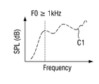
상기 제1 메인 음향 발생 장치에 의해 출력된 음향의 F0는 상기 제1 서브 음향 발생 장치에 의해 출력된 음향의 F0와 상기 제2 서브 음향 발생 장치에 의해 출력된 음향의 F0보다 높다.The F0 of the sound output by the first main sound generator is higher than the F0 of the sound output by the first sub-sound generator and the F0 of the sound output by the second sub-sound generator.
상기 제1 메인 음향 발생 장치는 상기 제1 서브 음향 발생 장치와 상기 제2 서브 음향 발생 장치보다 고주파수 영역에서 음압 레벨이 높으며, 상기 제1 서브 음향 발생 장치와 상기 제2 서브 음향 발생 장치는 상기 제1 메인 음향 발생 장치보다 상기 고주파수 영역보다 낮은 저주파수 영역에서 상기 음압 레벨이 높다.The first main sound generator has a higher sound pressure level in the high frequency region than the first sub sound generator and the second sub sound generator, and the first sub sound generator and the second sub sound generator are the first 1 The sound pressure level is higher in the low frequency region lower than the high frequency region than the main sound generator.
상기 제2 지향 모드에서 상기 제2 서브 음향 발생 장치에 의해 상기 제1 메인 음향 발생 장치의 음향과 역위상을 갖는 음파가 출력되고, 상기 제3 지향 모드에서 상기 제1 서브 음향 발생 장치에 의해 상기 제1 메인 음향 발생 장치의 음향과 역위상을 갖는 음파가 출력된다.In the second directional mode, the second sub-sound generator outputs sound waves having an inverse phase with the sound of the first main sound generator, and in the third directional mode, the sound is generated by the first sub-sound generator. The sound of the first main sound generating device and sound waves having an inverse phase are output.
상기 표시 패널의 하부에 배치되는 완충 부재와 상기 완충 부재의 하부에 배치되는 방열 부재를 포함하는 패널 하부 부재를 더 구비하고, 상기 제1 메인 음향 발생 장치, 상기 제1 서브 음향 발생 장치, 및 상기 제2 서브 음향 발생 장치는 상기 완충 부재의 하부에 배치되며, 상기 방열 부재와 중첩하지 않는다.A panel lower member including a buffer member disposed under the display panel and a heat dissipation member disposed under the buffer member is further provided, and the first main sound generating device, the first sub sound generating device, and the The second sub-sound generating device is disposed under the buffer member and does not overlap the heat dissipation member.
상기 표시 패널은 상기 제1 메인 음향 발생 장치가 배치되는 제1 메인 진동 영역, 상기 제1 서브 음향 발생 장치가 배치되는 제1 서브 진동 영역, 상기 제2 서브 음향 발생 장치가 배치되는 제2 서브 진동 영역, 및 상기 제1 메인 진동 영역과 상기 제1 서브 진동 영역 사이와 상기 제1 메인 진동 영역과 상기 제2 서브 진동 영역 사이에 배치되는 전파 차단 영역을 포함한다.The display panel includes a first main vibration region in which the first main sound generator is disposed, a first sub vibration region in which the first sub sound generator is disposed, and a second sub vibration in which the second sub sound generator is disposed. And a radio wave blocking region disposed between the first main vibration region and the first sub vibration region and between the first main vibration region and the second sub vibration region.
상기 표시 패널의 하부에 배치되는 완충 부재와 상기 완충 부재의 하부에 배치되는 방열 부재를 포함하는 패널 하부 부재를 더 구비하고, 상기 전파 차단 영역에서 상기 완충 부재와 상기 방열 부재는 제거된다.A panel lower member including a buffer member disposed under the display panel and a heat dissipation member disposed under the buffer member is further provided, and the buffer member and the heat radiation member are removed from the radio wave blocking region.
상기 표시 패널은 하부 기판, 상기 하부 기판 상에 배치되는 박막 트랜지스터층, 상기 박막 트랜지스터층 상에 배치되는 발광 소자층, 상기 발광 소자층 상에 배치되는 박막 봉지층을 포함하며, 상기 전파 차단 영역에서 상기 하부 기판은 제거된다.The display panel includes a lower substrate, a thin film transistor layer disposed on the lower substrate, a light emitting device layer disposed on the thin film transistor layer, and a thin film encapsulation layer disposed on the light emitting device layer. The lower substrate is removed.
상기 전파 차단 영역에서 상기 박막 트랜지스터층, 상기 발광 소자층, 및 상기 박막 봉지층은 제거된다.The thin film transistor layer, the light emitting device layer, and the thin film encapsulation layer are removed from the radio wave blocking region.
상기 제1 메인 진동 영역, 상기 제1 서브 진동 영역, 및 상기 제2 서브 진동 영역에서 상기 박막 봉지층은 상기 박막 트랜지스터층의 측면들과 상기 발광 소자층의 상면과 측면들을 덮는다.In the first main vibration region, the first sub vibration region, and the second sub vibration region, the thin film encapsulation layer covers side surfaces of the thin film transistor layer and top and side surfaces of the light emitting device layer.
상기 표시 패널의 하부에 배치되는 완충 부재와 상기 완충 부재의 하부에 배치되는 방열 부재를 포함하는 패널 하부 부재를 더 구비하고, 상기 완충 부재는 상기 전파 차단 영역에서 상기 완충 부재의 일면에 오목하게 형성되는 복수의 홈들을 포함한다.A panel lower member including a buffer member disposed under the display panel and a heat dissipation member disposed under the buffer member is further provided, and the buffer member is concavely formed on one surface of the buffer member in the radio wave blocking region. It includes a plurality of grooves.
상기 복수의 홈들을 채우며, 상기 완충 부재보다 낮은 밀도를 갖는 저밀도 물질을 더 구비한다.Filling the plurality of grooves, it is further provided with a low density material having a lower density than the buffer member.
상기 복수의 홈들 각각의 적어도 일부를 채우는 금속층을 더 구비한다.A metal layer filling at least a portion of each of the plurality of grooves is further provided.
상기 금속층과 상기 제1 메인 음향 발생 장치를 연결하는 제1 연성 회로 보드를 더 구비한다.A first flexible circuit board connecting the metal layer and the first main sound generating device is further provided.
상기 복수의 홈들 각각에 채워진 상기 금속층 상에 배치되는 보호층을 더 구비한다.A protective layer disposed on the metal layer filled in each of the plurality of grooves is further provided.
상기 제1 메인 음향 발생 장치, 상기 제1 서브 음향 발생 장치, 및 상기 제2 서브 음향 발생 장치 각각은 제1 구동 전압이 인가되는 제1 전극, 제2 구동 전압이 인가되는 제2 전극, 및 상기 제1 전극과 상기 제2 전극 사이에 배치되며 상기 제1 전극에 인가되는 제1 구동 전압과 상기 제2 전극에 인가되는 제2 구동 전압에 따라 수축 또는 팽창하는 진동층을 포함한다.Each of the first main sound generator, the first sub sound generator, and the second sub sound generator is a first electrode to which a first driving voltage is applied, a second electrode to which a second driving voltage is applied, and the It is disposed between the first electrode and the second electrode and includes a vibration layer that contracts or expands according to a first driving voltage applied to the first electrode and a second driving voltage applied to the second electrode.
상기 제1 메인 음향 발생 장치의 제1 전극과 제2 전극에 전기적으로 연결되는 제1 연성 회로 보드를 더 구비한다.The first flexible circuit board is further electrically connected to the first electrode and the second electrode of the first main sound generator.
상기 표시 패널은 기판, 상기 기판의 일 측에 부착되는 연성 필름, 및 상기 연성 필름에 전기적으로 연결되는 제어 회로 보드를 포함하고, 상기 제1 연성 회로 보드는 상기 제어 회로 보드 상에 배치된 커넥터에 접속된다.The display panel includes a substrate, a flexible film attached to one side of the substrate, and a control circuit board electrically connected to the flexible film, wherein the first flexible circuit board is connected to a connector disposed on the control circuit board. Connected.
상기 또 다른 과제를 해결하기 위한 일 실시예에 따른 표시 장치의 구동 방법은 카메라 센서를 이용하여 표시 장치의 전면(前面)의 배경을 촬영하는 단계, 상기 카메라 센서에 의해 촬영된 이미지를 분석하여 사용자의 위치를 판단하는 단계, 사용자가 표시 장치의 중앙의 전면(前面)에 위치하는 경우, 표시 장치의 중앙에 인접하게 배치된 제1 메인 음향 발생 장치에 의해 음향을 출력하는 단계, 사용자가 상기 표시 장치의 제1 측의 전면(前面)에 위치하는 경우, 상기 제1 메인 음향 발생 장치와 상기 제1 메인 음향 발생 장치보다 상기 표시 장치의 제1 측에 인접하게 배치된 제1 서브 음향 발생 장치에 의해 음향을 출력하는 단계, 및 사용자가 상기 표시 장치의 제2 측의 전면에 위치하는 경우, 상기 제1 메인 음향 발생 장치와 상기 제1 메인 음향 발생 장치보다 상기 표시 장치의 제2 측에 인접하게 배치된 제2 서브 음향 발생 장치에 의해 음향을 출력하는 단계를 포함한다.A method of driving a display device according to an embodiment of the present invention for solving the above another subject is a step of photographing a background of a front surface of a display device using a camera sensor, and analyzing an image captured by the camera sensor Determining the position of, If the user is located on the front (front) of the center of the display device, outputting sound by the first main sound generating device disposed adjacent to the center of the display device, the user displays the When located on the front side of the first side of the device, the first main sound generating device and the first sub sound generating device disposed closer to the first side of the display device than the first main sound generating device Outputting sound, and when the user is located on the front side of the second side of the display device, the first main sound generating device and the first main sound generating device It comprises the steps of outputting sound by the second side adjacent to the second sub-arranged sound-generating device of the display device.
기타 실시예의 구체적인 사항들은 상세한 설명 및 도면들에 포함되어 있다.Specific details of other embodiments are included in the detailed description and drawings.
일 실시예에 따른 표시 장치와 그의 구동 방법에 의하면, 표시 패널의 하부에 복수의 음향 발생 장치들을 배치하고, 음향 지향 모드에 따라 복수의 음향 발생 장치들의 음향 출력 여부를 결정함으로써, 음향을 특정한 방향으로 지향(指向)하여 출력할 수 있다.According to a display device and a driving method thereof according to an embodiment, a plurality of sound generating devices are disposed under the display panel, and the sound is directed to a specific direction by determining whether to output sound from the sound generating devices according to the sound directing mode You can output by directing to.
또한, 일 실시예에 따른 표시 장치와 그의 구동 방법에 의하면, 전파 차단 영역은 서로 인접한 진동 영역들 사이에 배치되므로, 전파 차단 영역에 의해 어느 한 진동 영역의 음향 발생 장치에 의한 진동이 다른 진동 영역들로 전파되는 것을 차단할 수 있다. 따라서, 어느 한 진동 영역의 음향 발생 장치에 의해 다른 진동 영역의 음향 발생 장치에 의한 음향 출력이 영향을 받는 것을 방지할 수 있다.In addition, according to the display device and the driving method according to an embodiment, since the radio wave blocking region is disposed between adjacent vibration regions, the vibration due to the sound generating device of one vibration region is different from the radio wave blocking region. It can block propagation. Therefore, it is possible to prevent the sound output by the sound generating device in another vibration area from being affected by the sound generating device in one vibration area.
실시예들에 따른 효과는 이상에서 예시된 내용에 의해 제한되지 않으며, 더욱 다양한 효과들이 본 명세서 내에 포함되어 있다.The effects according to the embodiments are not limited by the contents exemplified above, and more various effects are included in the present specification.
도 1은 일 실시예에 따른 표시 장치를 보여주는 사시도이다.
도 2는 도 1의 표시 장치의 분해 사시도이다.
도 3은 도 2에 도시된 연성 필름들이 구부러지지 않은 경우 표시 패널의 일 예를 보여주는 저면도이다.
도 4는 도 2에 도시된 연성 필름들이 구부러진 경우 표시 패널의 일 예를 보여주는 저면도이다.
도 5는 도 3의 제1 메인 음향 발생 장치의 일 예를 보여주는 사시도이다.
도 6은 도 3의 제1 메인 음향 발생 장치의 일 예를 보여주는 평면도이다.
도 7 도 5의 Ⅰ-Ⅰ’의 일 예를 보여주는 단면도이다.
도 8은 제1 메인 음향 발생 장치의 제1 가지 전극과 제2 가지 전극 사이에 배치된 진동층의 진동 방법을 보여주는 예시도면이다.
도 9와 도 10은 제1 메인 음향 발생 장치의 진동에 의한 표시 패널의 진동 방법을 보여주는 예시도면이다.
도 11은 일 실시예에 따른 표시 장치를 보여주는 블록도이다.
도 12는 일 실시예에 따른 표시 장치의 구동 방법을 보여주는 흐름도이다.
도 13a 내지 도 13e는 사용자가 표시 장치의 중앙, 제1 측, 제2 측, 제3 측, 제4 측의 전면에 위치하는 경우, 음향 발생 장치들의 음향 출력 여부를 보여주는 일 예시도면이다.
도 14는 일 실시예에 따른 제1 메인 음향 발생 장치에 의해 출력된 음향의 노이즈 캔슬링을 설명하기 위한 일 예시도면이다.
도 15는 일 실시예에 따른 음향 발생 장치들 각각의 주파수에 따른 음압 레벨을 보여주는 그래프이다.
도 16a, 도 16b, 및 도 16c는 메인 음향 발생 장치의 음향의 주파수에 따른 음압 레벨, 서브 음향 발생 장치의 음향의 주파수에 따른 음압 레벨, 및 메인 음향 발생 장치의 음향과 서브 음향 발생 장치의 음향이 합산된 음향의 주파수에 따른 음압 레벨을 보여주는 그래프들이다.
도 17은 도 2에 도시된 표시 패널의 또 다른 예를 보여주는 저면도이다.
도 18은 도 2에 도시된 표시 패널의 또 다른 예를 보여주는 저면도이다.
도 19는 도 2에 도시된 표시 패널의 또 다른 예를 보여주는 저면도이다.
도 20은 도 2에 도시된 표시 패널의 또 다른 예를 보여주는 저면도이다.
도 21은 도 20의 Ⅱ-Ⅱ’의 일 예를 보여주는 단면도이다.
도 22는 도 21의 표시 패널을 상세히 보여주는 확대 단면도이다.
도 23은 도 22의 Ⅱ-Ⅱ’의 또 다른 예를 보여주는 단면도이다.
도 24는 도 22의 Ⅱ-Ⅱ’의 또 다른 예를 보여주는 단면도이다.
도 25는 도 2에 도시된 표시 패널의 또 다른 예를 보여주는 저면도이다.
도 26은 도 25의 Ⅲ-Ⅲ’의 일 예를 보여주는 단면도이다.
도 27은 도 25의 Ⅲ-Ⅲ’의 다른 예를 보여주는 단면도이다.
도 28은 도 2에 도시된 표시 패널의 또 다른 예를 보여주는 저면도이다.
도 29는 도 28의 Ⅳ-Ⅳ’의 일 예를 보여주는 단면도이다.
도 30은 도 28의 Ⅴ-Ⅴ’의 일 예를 보여주는 단면도이다.
도 31은 표시 패널에 표시되는 영상에 따른 음향 발생 장치들의 음향 출력 여부를 보여주는 일 예시도면이다.1 is a perspective view showing a display device according to an exemplary embodiment.
2 is an exploded perspective view of the display device of FIG. 1.
3 is a bottom view illustrating an example of a display panel when the flexible films illustrated in FIG. 2 are not bent.
4 is a bottom view showing an example of a display panel when the flexible films illustrated in FIG. 2 are bent.
5 is a perspective view illustrating an example of the first main sound generator of FIG. 3.
6 is a plan view showing an example of the first main sound generator of FIG. 3.
7 is a cross-sectional view showing an example of Ⅰ-Ⅰ 'in FIG.
8 is an exemplary view showing a vibration method of a vibration layer disposed between a first branch electrode and a second branch electrode of the first main sound generating device.
9 and 10 are exemplary views showing a vibration method of a display panel by vibration of the first main sound generating device.
11 is a block diagram illustrating a display device according to an exemplary embodiment.
12 is a flowchart illustrating a method of driving a display device according to an exemplary embodiment.
13A to 13E are exemplary views showing whether sound is output from the sound generating devices when the user is located at the front of the center, the first side, the second side, the third side, and the fourth side of the display device.
14 is an exemplary view for explaining noise canceling of sound output by the first main sound generating apparatus according to an embodiment.
15 is a graph showing a sound pressure level according to each frequency of sound generating devices according to an embodiment.
16A, 16B, and 16C are sound pressure levels according to the frequency of the sound of the main sound generator, sound pressure levels according to the frequency of the sound of the sub sound generator, and the sound of the main sound generator and the sound of the sub sound generator These graphs show the sound pressure level according to the frequency of the summed sound.
17 is a bottom view illustrating still another example of the display panel illustrated in FIG. 2.
18 is a bottom view illustrating still another example of the display panel illustrated in FIG. 2.
19 is a bottom view illustrating another example of the display panel illustrated in FIG. 2.
20 is a bottom view illustrating another example of the display panel illustrated in FIG. 2.
21 is a cross-sectional view showing an example of II-II 'in FIG. 20.
22 is an enlarged cross-sectional view illustrating in detail the display panel of FIG. 21.
23 is a cross-sectional view showing another example of II-II 'of FIG. 22.
24 is a cross-sectional view showing another example of II-II 'of FIG. 22.
25 is a bottom view illustrating still another example of the display panel illustrated in FIG. 2.
26 is a cross-sectional view showing an example of III-III 'of FIG. 25.
27 is a cross-sectional view showing another example of III-III 'in FIG. 25.
28 is a bottom view illustrating still another example of the display panel illustrated in FIG. 2.
29 is a cross-sectional view showing an example of IV-IV 'of FIG. 28.
30 is a cross-sectional view showing an example of V-V 'of FIG. 28.
31 is an exemplary view showing whether sound is output from sound generating devices according to an image displayed on a display panel.
본 발명의 이점 및 특징, 그리고 그것들을 달성하는 방법은 첨부되는 도면과 함께 상세하게 후술되어 있는 실시예들을 참조하면 명확해질 것이다. 그러나 본 발명은 이하에서 개시되는 실시예들에 한정되는 것이 아니라 서로 다른 다양한 형태로 구현될 것이며, 단지 본 실시예들은 본 발명의 개시가 완전하도록 하며, 본 발명이 속하는 기술분야에서 통상의 지식을 가진 자에게 발명의 범주를 완전하게 알려주기 위해 제공되는 것이며, 본 발명은 청구항의 범주에 의해 정의될 뿐이다.Advantages and features of the present invention, and methods for achieving them will be clarified with reference to embodiments described below in detail together with the accompanying drawings. However, the present invention is not limited to the embodiments disclosed below, but will be implemented in various different forms, and only the present embodiments allow the disclosure of the present invention to be complete, and the ordinary knowledge in the technical field to which the present invention pertains. It is provided to fully inform the holder of the scope of the invention, and the invention is only defined by the scope of the claims.
소자(elements) 또는 층이 다른 소자 또는 층의 "상(on)"으로 지칭되는 것은 다른 소자 바로 위에 또는 중간에 다른 층 또는 다른 소자를 개재한 경우를 모두 포함한다. 명세서 전체에 걸쳐 동일 참조 부호는 동일 구성 요소를 지칭한다. 실시예들을 설명하기 위한 도면에 개시된 형상, 크기, 비율, 각도, 개수 등은 예시적인 것이므로 본 발명이 도시된 사항에 한정되는 것은 아니다. An element or layer being referred to as the "on" of another element or layer includes all cases in which another layer or other element is interposed immediately above or in between. The same reference numerals refer to the same components throughout the specification. The shapes, sizes, ratios, angles, numbers, and the like disclosed in the drawings for describing the embodiments are exemplary and the present invention is not limited to the illustrated matters.
비록 제1, 제2 등이 다양한 구성요소들을 서술하기 위해서 사용되나, 이들 구성요소들은 이들 용어에 의해 제한되지 않음은 물론이다. 이들 용어들은 단지 하나의 구성요소를 다른 구성요소와 구별하기 위하여 사용하는 것이다. 따라서, 이하에서 언급되는 제1 구성요소는 본 발명의 기술적 사상 내에서 제2 구성요소일 수도 있음은 물론이다.Although the first, second, etc. are used to describe various components, it goes without saying that these components are not limited by these terms. These terms are only used to distinguish one component from another component. Therefore, it goes without saying that the first component mentioned below may be the second component within the technical spirit of the present invention.
본 발명의 여러 실시예들의 각각 특징들이 부분적으로 또는 전체적으로 서로 결합 또는 조합 가능하고, 기술적으로 다양한 연동 및 구동이 가능하며, 각 실시예들이 서로에 대하여 독립적으로 실시 가능할 수도 있고 연관 관계로 함께 실시할 수도 있다.Each of the features of the various embodiments of the present invention may be partially or wholly combined or combined with each other, technically various interlocking and driving may be possible, and each of the embodiments may be independently performed with respect to each other or may be implemented together in an association relationship. It might be.
이하 첨부된 도면을 참조하여 구체적인 실시예들에 대해 설명한다. Hereinafter, specific embodiments will be described with reference to the accompanying drawings.
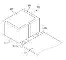
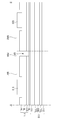
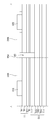
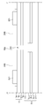
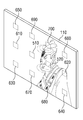
도 1은 일 실시예에 따른 표시 장치를 보여주는 사시도이다. 도 2는 도 1의 표시 장치의 분해 사시도이다. 도 3은 도 2에 도시된 연성 필름들이 구부러지지 않은 경우 표시 패널의 일 예를 보여주는 저면도이다. 도 4는 도 2에 도시된 연성 필름들이 구부러진 경우 표시 패널의 일 예를 보여주는 저면도이다. 한편, 도 3과 도 4는 저면도이므로, 도 3과 도 4에서는 도 1과 도 2와 비교할 때 표시 장치(10)의 좌우가 반대로 도시되어 있음에 주의하여야 한다.1 is a perspective view showing a display device according to an exemplary embodiment. 2 is an exploded perspective view of the display device of FIG. 1. 3 is a bottom view illustrating an example of a display panel when the flexible films illustrated in FIG. 2 are not bent. 4 is a bottom view showing an example of a display panel when the flexible films illustrated in FIG. 2 are bent. Meanwhile, since FIGS. 3 and 4 are bottom views, it should be noted that in FIGS. 3 and 4, the left and right sides of the
일 실시예에 따른 표시 장치(10)는 발광 소자로 유기 발광 소자를 이용하는 유기 발광 표시 장치 또는 발광 소자로 마이크로 발광 다이오드(무기 발광 다이오드)를 이용하는 마이크로 발광 표시 장치(무기 발광 표시 장치)일 수 있으나, 본 발명은 이에 한정되지 않는다. 이하에서는, 일 실시예에 따른 표시 장치(10)가 유기 발광 표시 장치인 것을 중심으로 설명하였다.The
도 1 내지 도 4를 참조하면, 일 실시예에 따른 표시 장치(10)는 커버 프레임(100), 표시 패널(110), 소스 구동 회로(121), 연성 필름(122), 소스 회로 보드(140), 연성 케이블(150), 제어 회로 보드(160), 타이밍 제어 회로(170), 및 카메라 센서(200)를 포함한다.1 to 4, the
본 명세서에서, “상부”, “탑”, “상면”은 표시 패널(110)의 하부 기판(111)을 기준으로 상부 기판(112)이 배치되는 방향, 즉 Z축 방향을 가리키고, “하부”, “바텀”, “하면”은 표시 패널(110)의 상부 기판(112)을 기준으로 하부 기판(111)이 배치되는 방향, 즉 Z축 방향의 반대 방향을 가리킨다. 또한, “좌”, “우”, “상”, “하”는 표시 패널(110)을 평면에서 바라보았을 때의 방향을 가리킨다. 예를 들어, “좌”는 X축 방향, “우”는 X축 방향의 반대 방향, “상”은 Y축 방향, “하”는 Y축 방향의 반대 방향을 가리킨다.In the present specification, “top”, “top”, and “top surface” indicate a direction in which the
커버 프레임(100)은 표시 패널(110)의 테두리를 둘러싸도록 배치될 수 있다. 즉, 커버 프레임(100)은 도 1 및 도 2와 같이 표시 패널(110)의 상면의 가장자리, 하면, 및 측면들을 덮도록 배치될 수 있다. 커버 프레임(100)은 표시 패널(110)의 표시 영역을 제외한 비표시 영역을 덮을 수 있다. 커버 프레임(100)은 플라스틱, 금속 또는 플라스틱과 금속을 포함할 수 있다.The
커버 프레임(100)은 도 2와 같이 상부 프레임(101)과 하부 프레임(102)을 포함할 수 있다. 상부 프레임(100)의 상면에는 카메라 센서(200)를 노출하기 위한 카메라 홀(CH)이 형성될 수 있다. 도 2에서는 카메라 홀(CH)이 상부 프레임(101)의 상 측에 형성되는 것을 예시하였으나, 본 발명은 이에 한정되지 않는다. 예를 들어, 카메라 홀(CH)은 상부 프레임(101)의 좌측, 우측 또는 하측에 형성될 수도 있다.The
표시 패널(110)은 평면 상 직사각형 형태로 이루어질 수 있다. 예를 들어, 표시 패널(110)은 도 2와 같이 제1 방향(X축 방향)의 장변과 제2 방향(Y축 방향)의 단변을 갖는 직사각형의 평면 형태를 가질 수 있다. 제1 방향(X축 방향)의 장변과 제2 방향(Y축 방향)의 단변이 만나는 모서리는 직각으로 형성되거나 소정의 곡률을 갖도록 둥글게 형성될 수 있다. 표시 패널(110)의 평면 형태는 직사각형에 한정되지 않고, 다른 다각형, 원형 또는 타원형으로 형성될 수 있다.The
도 2에서는 표시 패널(110)이 평탄하게 형성된 것을 예시하였으나, 본 발명은 이에 한정되지 않는다. 표시 패널(110)은 소정의 곡률로 구부러지도록 형성될 수 있다.2 illustrates that the
표시 패널(110)은 하부 기판(111)과 상부 기판(112)을 포함할 수 있다. 하부 기판(111)과 상부 기판(112)은 리지드(rigid)하거나 플렉시블(flexible)하게 형성될 수 있다. 하부 기판(111)은 유리 또는 플라스틱으로 형성될 수 있으며, 상부 기판(112)은 유리, 플라스틱, 봉지 필름, 또는 배리어 필름으로 형성될 수 있다. 플라스틱은 폴리에테르술폰(polyethersulphone: PES), 폴리아크릴레이트(polyacrylate: PA), 폴리아릴레이트(polyarylate: PAR), 폴리에테르이미드(polyetherimide: PEI), 폴리에틸렌나프탈레이트(polyethylenenapthalate: PEN), 폴리에틸렌 테레프탈레이드(polyethyleneterepthalate: PET), 폴리페닐렌설파이드 (polyphenylenesulfide: PPS), 폴리알릴레이트(polyallylate), 폴리이미드(polyimide: PI), 폴리카보네이트(polycarbonate: PC), 셀룰로오스 트리아세테이트(cellulosetriacetate: CAT), 셀룰로오스 아세테이트 프로피오네이트(cellulose acetate propionate: CAP) 또는 이들의 조합일 수 있다. 봉지 필름 또는 배리어 필름은 금속 봉지 필름 또는 복수의 무기막들이 적층된 필름일 수 있다.The
표시 패널(110)은 하부 기판(111)과 상부 기판(112) 사이에 배치된 박막 트랜지스터층, 발광 소자층, 및 박막 봉지층을 더 포함할 수 있다. 표시 패널(110)의 박막 트랜지스터층, 발광 소자층, 및 박막 봉지층에 대한 자세한 설명은 도 25를 결부하여 후술한다.The
하부 기판(111)의 크기가 상부 기판(112)의 크기보다 크기 때문에, 하부 기판(111)의 일 측은 상부 기판(112)에 의해 덮이지 않고 노출될 수 있다. 상부 기판(112)에 의해 덮이지 않고 노출된 하부 기판(111)의 일 측에는 연성 필름(122)들이 부착될 수 있다. 연성 필름(122)들 각각은 테이프 캐리어 패키지(tape carrier package) 또는 칩온 필름(chip on film)일 수 있다. 연성 필름(122)들 각각은 이방성 도전 필름(anisotropic conductive film)을 이용하여 TAB(tape automated bonding) 방식으로 하부 기판(111)상에 부착될 수 있으며, 이로 인해 소스 구동 회로(121)들은 데이터 라인들에 연결될 수 있다.Since the size of the
연성 필름(122)들 각각은 벤딩(bending)될 수 있다. 이로 인해, 연성 필름(122)들은 도 4와 같이 하부 기판(111)의 하면으로 벤딩(bending)될 수 있으며, 이 경우 소스 회로 보드(140), 연성 케이블(150)들, 및 제어 회로 보드(160)는 하부 기판(111)의 하면 상에 배치될 수 있다.Each of the
도 2에서는 8 개의 연성 필름(122)들이 표시 패널(110)의 하부 기판(111) 상에 부착되는 것을 예시하였으나, 본 발명의 연성 필름(122)들의 개수는 이에 한정되지 않는다.Although FIG. 2 illustrates that eight
연성 필름(122)들 각각의 일면 상에는 소스 구동 회로(121)가 장착될 수 있다. 소스 구동 회로(121)는 집적 회로(integrated circuit, IC)로 형성될 수 있다. 소스 구동 회로(121)는 타이밍 제어 회로(170)의 소스 제어 신호에 따라 디지털 비디오 데이터를 아날로그 데이터 전압들로 변환하여 연성 필름(122)을 통해 표시 패널(110)의 데이터 라인들에 공급한다.The
연성 필름(122)들 각각의 일 측은 표시 패널(110)의 하부 기판(111)의 일면 상에 부착되며, 타 측은 소스 회로 보드(140)의 일면 상에 부착될 수 있다. 소스 회로 보드(140)는 연성 케이블(150)들을 통해 제어 회로 보드(160)에 연결될 수 있다. 이를 위해, 소스 회로 보드(140)는 연성 케이블(150)들에 연결되기 위한 제1 커넥터(151)들을 포함할 수 있다. 소스 회로 보드(140)는 연성 인쇄회로보드(flexible printed circuit board) 또는 인쇄회로보드(printed circuit board)일 수 있다.One side of each of the
제어 회로 보드(160)는 연성 케이블(150)들을 통해 소스 회로 보드(140)에 연결될 수 있다. 이를 위해, 제어 회로 보드(160)는 연성 케이블(150)들에 연결되기 위한 제2 커넥터(152)들을 포함할 수 있다. 제어 회로 보드(160)는 연성 인쇄 회로 보드 또는 인쇄 회로 보드일 수 있다.The
도 2에서는 4 개의 연성 케이블(150)들이 소스 회로 보드(140)와 제어 회로 보드(160)를 연결하는 것을 예시하였으나, 본 발명의 연성 케이블(150)들의 개수는 이에 한정되지 않는다.Although FIG. 2 illustrates that four
제어 회로 보드(160)의 일면 상에는 타이밍 제어 회로(170)가 장착될 수 있다. 타이밍 제어 회로(170)는 집적 회로로 형성될 수 있다. 타이밍 제어 회로(170)는 시스템 온 칩으로부터 디지털 비디오 데이터와 타이밍 신호들을 입력 받으며, 타이밍 신호들에 따라 소스 구동 회로(121)들의 타이밍을 제어하기 위한 소스 제어 신호를 생성할 수 있다.The
시스템 온 칩은 다른 연성 케이블을 통해 제어 회로 보드(160)에 연결되는 시스템 회로 보드 상에 장착될 수 있으며, 집적 회로로 형성될 수 있다. 시스템 온 칩은 스마트 TV의 프로세서(processor), 컴퓨터 또는 노트북의 중앙 처리 장치(CPU) 또는 그래픽 카드, 또는 스마트폰 또는 태블릿 PC의 어플리케이션 프로세서(application processor)일 수 있다.The system-on-chip may be mounted on a system circuit board connected to the
제어 회로 보드(160)의 일면 상에는 전원 공급 회로가 추가로 장착될 수 있다. 전원 공급 회로는 시스템 회로 보드로부터 인가되는 메인 전원으로부터 표시 패널(110)의 구동에 필요한 전압들을 생성하여 표시 패널(110)에 공급할 수 있다. 예를 들어, 전원 공급 회로는 메인 전원으로부터 유기 발광 소자를 구동하기 위한 고전위 전압, 저전위 전압, 및 초기화 전압을 생성하여 표시 패널(110)에 공급할 수 있다. 또한, 전원 공급 회로는 메인 전원으로부터 소스 구동 회로(121)들, 타이밍 제어 회로(170) 등을 구동하기 위한 구동 전압들을 생성하여 공급할 수 있다. 전원 공급 회로는 집적 회로로 형성될 수 있다.A power supply circuit may be additionally mounted on one surface of the
카메라 센서(200)는 커버 프레임(100)의 카메라 홀(CH)에 배치될 수 있다. 이로 인해, 카메라 센서(200)는 표시 장치(10)의 전면(前面)의 배경을 촬영할 수 있다. 카메라 센서(200)는 CMOS 이미지 센서(Complementary Metal Oxide Semiconductor Image Sensor) 또는 CCD 이미지 센서(Charge Coupled Device Image Sensor)일 수 있다.The
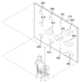
카메라 센서(200)는 시스템 회로 보드에 장착된 시스템 온 칩과 전기적으로 연결될 수 있다. 카메라 센서(200)는 그에 의해 촬영된 이미지를 시스템 온 칩으로 출력하며, 시스템 온 칩은 카메라 센서(200)에 의해 촬영된 이미지를 분석하여 사용자가 표시 장치의 중앙, 제1 측, 제2 측, 제3 측, 및 제4 측 중 어느 곳에서 전면에 위치하는지를 판단할 수 있다. 시스템 온 칩은 사용자의 위치에 따라 복수의 음향 발생 장치들의 음향 출력을 제어함으로써, 사용자의 위치로 음향을 지향하여 출력할 수 있다.The
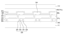
도 3 및 도 4와 같이 표시 패널(110)의 하면에는 복수의 음향 발생 장치들이 배치될 수 있다. 복수의 음향 발생 장치들은 상하로 진동을 발생시킬 수 있는 진동 발생 장치일 수 있다. 복수의 음향 발생 장치들 각각에 의해 표시 패널(110)을 상하로 진동함으로써 음향을 출력할 수 있다. 복수의 음향 발생 장치들은 편심 모터(eccentric rotating mass, ERM), 선형 공진 액츄에이터(linear resonant actuator, LRA), 피에조 액츄에이터(piezo actuator) 등으로 구현될 수 있다. 이하에서는, 복수의 음향 발생 장치들이 피에조 액츄에이터인 것을 중심으로 설명하였다.3 and 4, a plurality of sound generating devices may be disposed on the lower surface of the
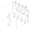
복수의 음향 발생 장치들은 제1 및 제2 메인 음향 발생 장치들(510, 520)과 제1 내지 제10 서브 음향 발생 장치들(610, 620, 630, 640, 650, 660, 670, 680, 690, 700)을 포함할 수 있다. 메인 음향 발생 장치들의 개수와 서브 음향 발생 장치들의 개수는 도 3 및 도 4에 도시된 바에 한정되지 않는다.The plurality of sound generating devices include first and second main
제1 및 제2 메인 음향 발생 장치들(510, 520)은 음향 지향 여부와 상관없이 음향을 출력할 수 있다. 즉, 제1 및 제2 메인 음향 발생 장치들(510, 520)은 표시 패널(110)의 중앙의 전면(前面)으로 음향을 출력하는 제1 지향 모드, 표시 패널(110)의 제1 측의 전면(前面)으로 음향을 출력하는 제2 지향 모드, 표시 패널(110)의 제2 측의 전면(前面)으로 음향을 출력하는 제3 지향 모드, 표시 패널(110)의 제3 측의 전면(前面)으로 음향을 출력하는 제4 지향 모드, 표시 패널(110)의 제4 측의 전면(前面)으로 음향을 출력하는 제5 지향 모드, 및 무지향 모드에서 음향을 출력할 수 있다. 여기서, 표시 패널(110)의 제1 측은 좌측, 제2 측은 우측, 제3 측은 하측, 제4 측은 상측 일 수 있다. 이에 비해, 제1 내지 제10 서브 음향 발생 장치들(610, 620, 630, 640, 650, 660, 670, 680, 690, 700)은 음향 지향 여부에 따라 음향 출력 여부가 결정될 수 있다. 제1 지향 모드, 제2 지향 모드, 제3 지향 모드, 제4 지향 모드, 제5 지향 모드, 및 무지향 모드 각각에서 제1 내지 제10 서브 음향 발생 장치들(610, 620, 630, 640, 650, 660, 670, 680, 690, 700)의 음향 출력 여부는 도 14a 내지 도 14e를 결부하여 상세히 설명한다.The first and second main
제1 및 제2 메인 음향 발생 장치들(510, 520) 각각은 제1 내지 제10 서브 음향 발생 장치들(610, 620, 630, 640, 650, 660, 670, 680, 690, 700)보다 표시 패널(110)의 중앙에 가깝게 배치될 수 있다. 제1 메인 음향 발생 장치(510)는 제2 메인 음향 발생 장치(520)보다 표시 패널(110)의 제1 측에 가깝게 배치되고, 제2 메인 음향 발생 장치(520)는 제1 메인 음향 발생 장치(510)보다 제2 측에 가깝게 배치될 수 있다.Each of the first and second main
제1 서브 음향 발생 장치(610), 제3 서브 음향 발생 장치(630), 및 제5 서브 음향 발생 장치(650)는 표시 패널(110)의 제1 측에 가깝게 배치될 수 있다. 예를 들어, 도 3과 같이 제1 서브 음향 발생 장치(610)는 표시 패널(110)의 좌측 중앙에 배치되고, 제3 서브 음향 발생 장치(630)는 표시 패널(110)의 하좌측에 배치되며, 제5 서브 음향 발생 장치(650)는 표시 패널(110)의 상좌측에 배치될 수 있다.The first
제2 서브 음향 발생 장치(620), 제4 서브 음향 발생 장치(640), 및 제6 서브 음향 발생 장치(660)는 표시 패널(110)의 제2 측에 가깝게 배치될 수 있다. 예를 들어, 도 3과 같이 제2 서브 음향 발생 장치(620)는 표시 패널(110)의 우측 중앙에 배치되고, 제4 서브 음향 발생 장치(640)는 표시 패널(110)의 하우측에 배치되며, 제6 서브 음향 발생 장치(660)는 표시 패널(110)의 상우측에 배치될 수 있다.The second
제7 서브 음향 발생 장치(670)는 제1 메인 음향 발생 장치(510)보다 표시 패널(110)의 제3 측에 가깝게 배치되며, 제8 서브 음향 발생 장치(680)는 제2 메인 음향 발생 장치(520)보다 표시 패널(110)의 제4 측에 가깝게 배치될 수 있다. 제9 서브 음향 발생 장치(690)는 제1 메인 음향 발생 장치(510)보다 표시 패널(110)의 제4 측에 가깝게 배치되며, 제10 서브 음향 발생 장치(700)는 제2 메인 음향 발생 장치(520)보다 표시 패널(110)의 제4 측에 가깝게 배치될 수 있다.The seventh
제1 및 제2 메인 음향 발생 장치들(510, 520)과 제1 내지 제10 서브 음향 발생 장치들(610, 620, 630, 640, 650, 660, 670, 680, 690, 700) 각각은 연성 회로 보드를 통해 제어 회로 보드(160)에 연결될 수 있다. 예를 들어, 제1 메인 음향 발생 장치(510), 제1 서브 음향 발생 장치(610), 제3 서브 음향 발생 장치(630), 제5 서브 음향 발생 장치(650), 제7 서브 음향 발생 장치(670), 및 제9 서브 음향 발생 장치(690)는 제1 연성 회로 보드(710)에 연결될 수 있으며, 제1 연성 회로 보드(710)의 제1 접속부(711)는 도 4와 같이 연성 필름(122)들이 표시 패널(110)의 하면으로 벤딩되어 표시 패널(110)의 하면 상에 배치된 제어 회로 보드(160)의 제3 커넥터(712)에 연결될 수 있다.Each of the first and second main
구체적으로, 제1 연성 회로 보드(710)는 제1 줄기부(710a)와 제1 줄기부(710a)로부터 분지되는 제1 내지 제7 가지부들(710b, 710c, 710d, 710e, 710f, 710g, 710h)을 포함할 수 있다. 제1 가지부(710b)는 제1 줄기부(710a)로부터 제2 측 방향으로 분지되어 제1 메인 음향 발생 장치(510)에 연결되고, 제2 가지부(710c)는 제1 줄기부(710a)로부터 제1 측 방향으로 분지되어 제1 서브 음향 발생 장치(610)에 연결될 수 있다. 제3 가지부(710d)는 제1 줄기부(710a)로부터 제1 측 방향으로 분지되어 제3 서브 음향 발생 장치(630)에 연결되고, 제4 가지부(710e)는 제1 줄기부(710a)로부터 제1 측 방향으로 분지되어 제5 서브 음향 발생 장치(650)에 연결될 수 있다. 제5 가지부(710f)는 제1 줄기부(710a)로부터 제2 측 방향으로 분지되어 제7 서브 음향 발생 장치(670)에 연결되고, 제6 가지부(710g)는 제1 줄기부(710a)로부터 제2 측 방향으로 분지되어 제9 서브 음향 발생 장치(690)에 연결될 수 있다. 제7 가지부(710h)는 제1 줄기부(710a)로부터 제2 측 방향으로 분지되어 제어 회로 보드(160)의 제3 커넥터(712)에 연결되며, 이를 위해 제7 가지부(710h)의 일 측 끝단에는 제1 접속부(711)가 형성될 수 있다.Specifically, the first
또한, 제2 메인 음향 발생 장치(520), 제2 서브 음향 발생 장치(520), 제4 서브 음향 발생 장치(540), 제6 서브 음향 발생 장치(560), 제8 서브 음향 발생 장치(580), 및 제10 서브 음향 발생 장치(600)는 제2 연성 회로 보드(720)에 연결될 수 있으며, 제2 연성 회로 보드(720)의 제2 접속부(721)는 도 4와 같이 연성 필름(122)들이 표시 패널(110)의 하면으로 벤딩되어 표시 패널(110)의 하면 상에 배치된 제어 회로 보드(160)의 제4 커넥터(722)에 연결될 수 있다.In addition, the second main
구체적으로, 제2 연성 회로 보드(720)는 제2 줄기부(720a)와 제2 줄기부(720a)로부터 분지되는 제8 내지 제14 가지부들(720b, 720c, 720d, 720e, 720f, 720g, 720h)을 포함할 수 있다. 제8 가지부(720b)는 제2 줄기부(720a)로부터 제1 측 방향으로 분지되어 제2 메인 음향 발생 장치(520)에 연결되고, 제9 가지부(720c)는 제2 줄기부(720a)로부터 제2 측 방향으로 분지되어 제2 서브 음향 발생 장치(620)에 연결될 수 있다. 제10 가지부(720d)는 제2 줄기부(720a)로부터 제2 측 방향으로 분지되어 제4 서브 음향 발생 장치(640)에 연결되고, 제11 가지부(720e)는 제2 줄기부(720a)로부터 제2 측 방향으로 분지되어 제6 서브 음향 발생 장치(660)에 연결될 수 있다. 제12 가지부(720f)는 제2 줄기부(720a)로부터 제1 측 방향으로 분지되어 제8 서브 음향 발생 장치(680)에 연결되고, 제13 가지부(720g)는 제2 줄기부(720a)로부터 제1 측 방향으로 분지되어 제10 서브 음향 발생 장치(700)에 연결될 수 있다. 제14 가지부(720h)는 제2 줄기부(720a)로부터 제1 측 방향으로 분지되어 제어 회로 보드(160)의 제4 커넥터(722)에 연결되며, 이를 위해 제14 가지부(720h)의 일 측 끝단에는 제2 접속부(721)가 형성될 수 있다.Specifically, the second
한편, 도 3 및 도 4에서는 복수의 음향 발생 장치들, 예를 들어 6 개의 음향 발생 장치들이 하나의 연성 회로 보드를 통해 제어 회로 보드(160)에 연결되는 것을 예시하였으나, 본 발명은 이에 한정되지 않는다. 예를 들어, 제1 및 제2 메인 음향 발생 장치들(510, 520)과 제1 내지 제10 서브 음향 발생 장치들(610, 620, 630, 640, 650, 660, 670, 680, 690, 700)이 각각 별도의 연성 회로 보드를 통해 제어 회로 보드(160)에 연결될 수 있다.Meanwhile, FIGS. 3 and 4 illustrate that a plurality of sound generating devices, for example, six sound generating devices are connected to the
도 3 및 도 4에 도시된 실시예에 의하면, 표시 패널(110)의 하부에 복수의 음향 발생 장치들을 배치하고, 음향 지향 모드에 따라 복수의 음향 발생 장치들의 음향 출력 여부를 결정하므로, 음향을 특정한 방향으로 지향(指向)하여 출력할 수 있다.According to the embodiment illustrated in FIGS. 3 and 4, since a plurality of sound generating devices are disposed under the
도 5는 도 3의 제1 메인 음향 발생 장치의 일 예를 보여주는 사시도이다. 도 6은 도 3의 제1 메인 음향 발생 장치의 일 예를 보여주는 평면도이다. 도 7 도 5의 Ⅰ-Ⅰ’의 일 예를 보여주는 단면도이다.5 is a perspective view illustrating an example of the first main sound generator of FIG. 3. 6 is a plan view showing an example of the first main sound generator of FIG. 3. 7 is a cross-sectional view showing an example of Ⅰ-Ⅰ 'in FIG. 5.
도 5, 도 6 및 도 7을 참조하면, 제1 메인 음향 발생 장치(510)는 진동층(511), 제1 전극(512), 제2 전극(513), 제1A 패드 전극(512a), 및 제2A 패드 전극(513a)을 포함할 수 있다.5, 6 and 7, the first main
제1 전극(512)은 제1 줄기 전극(5121)과 제1 가지 전극(5122)들을 포함할 수 있다. 제1 줄기 전극(5121)은 진동층(511)의 일 측면에만 배치되거나 도 5 및 도 6과 같이 진동층(511)의 복수의 측면들에 배치될 수 있다. 제1 줄기 전극(5121)은 진동층(511)의 상면에 배치될 수도 있다. 제1 가지 전극(5122)들은 제1 줄기 전극(5121)으로부터 분지될 수 있다. 제1 가지 전극(5122)들은 서로 나란하게 배치될 수 있다.The
제2 전극(513)은 제2 줄기 전극(5131)과 제2 가지 전극(5132)들을 포함할 수 있다. 제2 줄기 전극(5131)은 진동층(511)의 다른 일 측면에 배치되거나 도 5 및 도 6과 같이 진동층(511)의 복수의 측면들에 배치될 수도 있다. 이때, 도 5 및 도 6과 같이 제2 줄기 전극(5131)이 배치되는 복수의 측면들 중 어느 한 측면에는 제1 줄기 전극(5121)이 배치될 수 있다. 제2 줄기 전극(5131)은 진동층(511)의 상면에 배치될 수 있다. 제1 줄기 전극(5121)과 제2 줄기 전극(5131)은 서로 중첩되지 않을 수 있다. 제2 가지 전극(5132)들은 제2 줄기 전극(5131)으로부터 분지될 수 있다. 제2 가지 전극(5132)들은 서로 나란하게 배치될 수 있다.The
제1 가지 전극(5122)들과 제2 가지 전극(5132)들은 수평 방향(X축 방향 또는 Y축 방향)으로 서로 나란하게 배치될 수 있다. 또한, 제1 가지 전극(5122)들과 제2 가지 전극(5132)들은 수직 방향(Z축 방향)에서 교대로 배치될 수 있다. 즉, 제1 가지 전극(5122)들과 제2 가지 전극(5132)들은 수직 방향(Z축 방향)에서 제1 가지 전극(5122), 제2 가지 전극(5132), 제1 가지 전극(5122), 제2 가지 전극(5132)의 순서로 반복적으로 배치될 수 있다.The first branch electrodes 5202 and the
제1A 패드 전극(512a)은 제1 전극(512)에 연결될 수 있다. 제1A 패드 전극(512a)은 진동층(511)의 일 측면에 배치된 제1 줄기 전극(5121)으로부터 외측 방향으로 돌출될 수 있다. 제2A 패드 전극(513a)은 제2 전극(513)에 연결될 수 있다. 제2A 패드 전극(513a)은 진동층(511)의 일 측면에 배치된 제2 줄기 전극(5131)으로부터 외측 방향으로 돌출될 수 있다. 즉, 제1A 패드 전극(512a)과 제2A 패드 전극(513a)은 각각 진동층(511)의 동일한 측면에 배치된 제1 줄기 전극(5121)과 제2 줄기 전극(5131)으로부터 각각 외측 방향으로 돌출될 수 있다.The
제1A 패드 전극(512a)과 제2A 패드 전극(513a)은 제1 연성 회로 보드(710)의 리드 라인들 또는 패드 전극들에 연결될 수 있다. 제1 연성 회로 보드(710)의 리드 라인들 또는 패드 전극들은 제1 음향 회로 보드(530)의 하면 상에 배치될 수 있다.The
진동층(511)은 제1 전극(512)에 인가된 제1 구동 전압과 제2 전극(513)에 인가되는 제2 구동 전압에 따라 변형되는 피에조 액츄에이터(piezo actuator)일 수 있다. 이 경우, 진동층(511)은 PVDF(Poly Vinylidene Fluoride) 필름이나 PZT(Plumbum Ziconate Titanate(티탄산지르콘납)) 등의 압전체, 전기 활성 고분자(Electro Active Polymer) 중 어느 하나일 수 있다.The
진동층(511)의 제조 온도가 높기 때문에, 제1 전극(512)과 제2 전극(513)은 녹는점이 높은 은(Ag) 또는 은(Ag)과 팔라듐(Pd)의 합금으로 형성될 수 있다. 제1 전극(512)과 제2 전극(513)의 녹는점을 높이기 위해, 제1 전극(512)과 제2 전극(513)이 은(Ag)과 팔라듐(Pd)의 합금으로 형성되는 경우, 은(Ag)의 함량이 팔라듐(Pd)의 함량보다 높을 수 있다.Since the manufacturing temperature of the
진동층(511)은 제1 가지 전극(5122)들과 제2 가지 전극(5132)들 사이마다 배치될 수 있다. 진동층(511)은 제1 가지 전극(5122)에 인가되는 제1 구동 전압과 제2 가지 전극(5132)에 인가되는 제2 구동 전압 간의 차이에 따라 수축하거나 팽창한다.The
구체적으로, 도 7과 같이 제1 가지 전극(5122)과 제1 가지 전극(5122)의 하부에 배치된 제2 가지 전극(5132) 사이에 배치된 진동층(511)의 극성 방향은 상부 방향(↑)일 수 있다. 이 경우, 진동층(511)은 제1 가지 전극(5122)에 인접한 상부 영역에서 정극성을 가지며, 제2 가지 전극(5132)에 인접한 하부 영역에서 부극성을 가진다. 또한, 제2 가지 전극(5132)과 제2 가지 전극(5132)의 하부에 배치된 제1 가지 전극(5122) 사이에 배치된 진동층(511)의 극성 방향은 하부 방향(↓)일 수 있다. 이 경우, 진동층(511)은 제2 가지 전극(5132)에 인접한 상부 영역에서 부극성을 가지며, 제1 가지 전극(5122)에 인접한 하부 영역에서 정극성을 가진다. 진동층(511)의 극성 방향은 제1 가지 전극(5122)과 제2 가지 전극(5132)을 이용하여 진동층(511)에 전계를 가하는 폴링(poling) 공정에 의해 정해질 수 있다.Specifically, as shown in FIG. 7, the polarity direction of the
도 8과 같이 제1 가지 전극(5122)과 제1 가지 전극(5122)의 하부에 배치된 제2 가지 전극(5132) 사이에 배치된 진동층(511)의 극성 방향이 상부 방향(↑)인 경우, 제1 가지 전극(5122)에 정극성의 제1 구동 전압이 인가되며, 제2 가지 전극(5132)에 부극성의 제2 구동 전압이 인가되면, 진동층(511)은 제1 힘(F1)에 따라 수축될 수 있다. 제1 힘(F1)은 수축력일 수 있다. 또한, 제1 가지 전극(5122)에 부극성의 제1 구동 전압이 인가되며, 제2 가지 전극(5132)에 정극성의 제2 구동 전압이 인가되면, 진동층(511)은 제2 힘(F2)에 따라 팽창할 수 있다. 제2 힘(F2)은 신장력일 수 있다.8, when the polarity direction of the
또한, 제2 가지 전극(5132)과 제2 가지 전극(5132)의 하부에 배치된 제1 가지 전극(5122) 사이에 배치된 진동층(511)의 극성 방향이 하부 방향(↓)인 경우, 제2 가지 전극(5132)에 정극성의 제1 구동 전압이 인가되며, 제1 가지 전극(5122)에 부극성의 제2 구동 전압이 인가되면, 진동층(511)은 신장력에 따라 팽창할 수 있다. 또한, 제2 가지 전극(5132)에 부극성의 제1 구동 전압이 인가되며, 제1 가지 전극(5122)에 정극성의 제2 구동 전압이 인가되면, 진동층(511)은 수축력에 따라 수축될 수 있다. 제2 힘(F2)은 신장력일 수 있다.In addition, when the polarity direction of the
도 5, 도 6, 및 도 7에 도시된 실시예에 의하면, 제1 전극(512)에 인가되는 제1 구동 전압과 제2 전극(513)에 인가되는 제2 구동 전압이 정극성과 부극성으로 교대로 반복되는 경우, 진동층(511)은 수축과 팽창을 반복하게 된다. 이로 인해, 제1 메인 음향 발생 장치(510)는 진동하게 된다.5, 6, and 7, the first driving voltage applied to the
제1 메인 음향 발생 장치(510)가 표시 패널(300)의 하면에 배치되므로, 제1 메인 음향 발생 장치(510)의 진동층(511)이 수축과 팽창하는 경우, 표시 패널(300)은 도 9 및 도 10과 같이 응력에 의해 하부와 상부로 진동하게 된다. 이와 같이, 제1 음향 발생 장치(510)에 의해 표시 패널(300)이 진동할 수 있으므로, 표시 장치(10)는 음향을 출력할 수 있다.Since the first
한편, 제2 메인 음향 발생 장치(520)와 제1 내지 제10 서브 음향 발생 장치들(610, 620, 630, 640, 650, 660, 670, 680, 690, 700)은 도 5, 도 6, 도 7, 도 8, 도 9 및 도 10을 결부하여 설명한 제1 메인 음향 발생 장치(510)와 실질적으로 동일할 수 있으므로, 이에 대한 자세한 설명은 생략한다.Meanwhile, the second main
도 11은 일 실시예에 따른 표시 장치를 보여주는 블록도이다.11 is a block diagram illustrating a display device according to an exemplary embodiment.
도 11을 참조하면, 일 실시예에 따른 표시 장치(10)는 표시 패널(110), 데이터 구동부(120), 스캔 구동부(130), 타이밍 제어 회로(170), 시스템 온 칩(180), 및 카메라 센서(200)를 포함한다.Referring to FIG. 11, the
표시 패널(110)은 표시 영역(DA)과 표시 영역(DA)의 주변에 배치된 비표시 영역(NDA)으로 구분될 수 있다. 표시 영역(DA)은 화소(P)들이 형성되어 화상을 표시하는 영역이다. 표시 패널(110)은 데이터 라인들(D1~Dm, m은 2 이상의 정수), 데이터 라인들(D1~Dm)과 교차되는 스캔 라인들(S1~Sn, n은 2 이상의 정수), 및 데이터 라인들(D1~Dm)과 스캔 라인들(S1~Sn)에 접속된 화소(P)들을 포함할 수 있다.The
화소(P)들 각각은 데이터 라인들(D1~Dm) 중 적어도 하나와 스캔 라인들(S1~Sn) 중 적어도 하나에 접속될 수 있다. 표시 패널(110)의 화소(P)들 각각은 유기 발광 소자(organic light emitting element)와 유기 발광 소자에 전류를 공급하기 위한 복수의 트랜지스터들과 적어도 하나의 커패시터를 포함할 수 있다. 유기 발광 소자는 제1 전극, 유기 발광층, 및 제2 전극을 포함하는 유기 발광 다이오드일 수 있다.Each of the pixels P may be connected to at least one of the data lines D1 to Dm and at least one of the scan lines S1 to Sn. Each of the pixels P of the
데이터 구동부(120)는 복수의 소스 구동 회로(121)들을 포함할 수 있다. 복수의 소스 구동 회로(121)들 각각은 타이밍 제어 회로(170)로부터 디지털 비디오 데이터(DATA)와 소스 제어 신호(DCS)를 입력 받는다. 복수의 소스 구동 회로(121)들 각각은 소스 제어 신호(DCS)에 따라 디지털 비디오 데이터(DATA)를 아날로그 데이터 전압들로 변환하여 표시 패널(110)의 데이터 라인들(D1~Dm)에 공급한다.The
스캔 구동부(130)는 타이밍 제어 회로(170)로부터 스캔 제어 신호(SCS)를 입력 받는다. 스캔 구동부는 스캔 제어 신호(SCS)에 따라 스캔 신호들을 생성하여 표시 패널(110)의 스캔 라인들(S1~Sn)에 공급한다. 스캔 구동부(130)는 다수의 트랜지스터들을 포함하여 표시 패널(110)의 비표시 영역(NDA)에 형성될 수 있다. 또는, 스캔 구동부(130)는 집적 회로로 형성될 수 있으며, 이 경우 표시 패널(110)의 하부 기판(111)에 부착되는 게이트 연성 필름 상에 장착될 수 있다.The
타이밍 제어 회로(170)는 시스템 온 칩(180)으로부터 디지털 비디오 데이터(DATA)와 타이밍 신호들을 입력받는다. 타이밍 신호들은 수직동기신호(vertical sync signal), 수평동기신호(horizontal sync signal), 데이터 인에이블 신호(data enable signal), 및 도트 클럭(dot clock)을 포함할 수 있다.The
타이밍 제어 회로(170)는 데이터 구동부(120)의 소스 구동 회로(121)들과 스캔 구동부(130)의 동작 타이밍을 제어하기 위한 제어신호들을 생성한다. 제어신호들은 데이터 구동부(120)의 소스 구동 회로(121)들의 동작 타이밍을 제어하기 위한 소스 제어 신호(DCS)와 스캔 구동부(130)의 동작 타이밍을 제어하기 위한 스캔 제어 신호(SCS)를 포함할 수 있다.The
카메라 센서(200)는 표시 장치(10)의 전면(前面)의 배경을 촬영하고, 촬영된 이미지(IM)를 시스템 온 칩(180)으로 출력할 수 있다.The
시스템 온 칩(180)은 카메라 센서(200)로부터 입력되는 이미지(IM)를 분석하여 사용자의 위치를 판단한다. 구체적으로, 시스템 온 칩(180)은 이미지(IM)를 분석하여 사용자가 표시 패널(110)의 중앙의 전면(前面), 제1 측의 전면(前面), 제2 측의 전면(前面), 제3 측의 전면(前面), 제4 측의 전면(前面) 중 어디에 위치하는지를 판단한다.The system on
구체적으로, 시스템 온 칩(180)은 사용자의 위치가 표시 패널(110)의 중앙의 전면(前面)에 위치하는 경우, 복수의 음향 발생 장치들의 음향이 표시 패널(110)의 중앙의 전면(前面)으로 지향되는 제1 지향 모드로 복수의 음향 발생 장치들을 제어할 수 있다. 시스템 온 칩(180)은 사용자의 위치가 표시 패널(110)의 제1 측의 전면(前面)에 위치하는 경우, 복수의 음향 발생 장치들의 음향이 표시 패널(110)의 제1 측의 전면(前面)으로 지향되는 제2 지향 모드로 복수의 음향 발생 장치들을 제어할 수 있다. 시스템 온 칩(180)은 사용자의 위치가 표시 패널(110)의 제2 측의 전면(前面)에 위치하는 경우, 복수의 음향 발생 장치들의 음향이 표시 패널(110)의 제2 측의 전면(前面)으로 지향되는 제3 지향 모드로 복수의 음향 발생 장치들을 제어할 수 있다. 시스템 온 칩(180)은 사용자의 위치가 표시 패널(110)의 제3 측의 전면(前面)에 위치하는 경우, 복수의 음향 발생 장치들의 음향이 표시 패널(110)의 제3 측의 전면(前面)으로 지향되는 제4 지향 모드로 복수의 음향 발생 장치들을 제어할 수 있다. 시스템 온 칩(180)은 사용자의 위치가 표시 패널(110)의 제4 측의 전면(前面)에 위치하는 경우, 복수의 음향 발생 장치들의 음향이 표시 패널(110)의 제4 측의 전면(前面)으로 지향되는 제5 지향 모드로 복수의 음향 발생 장치들을 제어할 수 있다.Specifically, in the system-on-
또한, 시스템 온 칩(180)은 사용자가 표시 패널(110)의 중앙의 전면(前面), 제1 측의 전면(前面), 제2 측의 전면(前面), 제3 측의 전면(前面), 제4 측의 전면(前面) 중 복수의 곳들에 위치하는 경우, 복수의 지향 모드들을 조합하여 복수의 음향 발생 장치들을 제어할 수 있다. 예를 들어, 시스템 온 칩(180)은 사용자의 위치가 표시 패널(110)의 중앙의 전면(前面)과 제1 측의 전면(前面)에 위치하는 경우, 복수의 음향 발생 장치들의 음향이 표시 패널(110)의 중앙의 전면(前面)으로 지향되는 제1 지향 모드와 제2 지향 모드로 복수의 음향 발생 장치들을 제어한다.In addition, the system-on-
나아가, 시스템 온 칩(180)은 사용자가 표시 패널(110)의 중앙의 전면(前面), 제1 측의 전면(前面), 제2 측의 전면(前面), 제3 측의 전면(前面), 제4 측의 전면(前面) 중 여러 곳에 위치하여 복수의 음향 발생 장치들이 음향을 지향하여 출력할 필요가 없는 경우, 무지향 모드로 복수의 음향 발생 장치들을 제어할 수 있다.Furthermore, the system-on-
시스템 온 칩(180)은 복수의 음향 발생 장치들을 제어하기 위한 음향 제어 신호(SOCS)를 생성하여 통합 음향 구동부(190)에 출력할 수 있다. 통합 음향 구동부(190)는 음향 제어 신호(SOCS)에 따라 복수의 음향 구동 신호들(MSDS1, MSDS2, SSDS1~SSDS10)을 생성하여 복수의 음향 발생 장치들에 출력할 수 있다.The system on
통합 음향 구동부(190)는 디지털 신호인 음향 제어 신호(SOCS)를 처리하는 디지털 신호 처리부(digital signal processer, DSP), 디지털 신호 처리부에서 처리된 디지털 신호를 아날로그 신호인 복수의 음향 구동 신호들(MSDS1, MSDS2, SSDS1~SSDS10)로 변환하는 디지털 아날로그 변환부(digital analog converter, DAC), 디지털 아날로그 변환부에서 변환된 아날로그 신호를 증폭하여 출력하는 증폭기(amplifier, AMP) 등을 포함할 수 있다.The
복수의 음향 구동 신호들(MSDS1, MSDS2, SSDS1~SSDS10)은 제1 메인 음향 발생 장치(510)를 구동하기 위한 제1 메인 음향 구동 신호(MSDS1)와 제2 메인 음향 발생 장치(520)를 구동하기 위한 제2 메인 음향 구동 신호(MSDS2)를 포함할 수 있다. 또한, 음향 제어 신호(SOCS)는 제1 내지 제10 서브 음향 발생 장치들(610, 620, 630, 640, 650, 660, 670, 680, 690, 700)을 구동하기 위한 제1 내지 제10 서브 음향 구동 신호들(SSDS1~SSDS10)을 더 포함할 수 있다.The plurality of sound driving signals MSDS1, MSDS2, and SSDS1 to SSDS10 drive the first main sound driving signal MSDS1 and the second main
복수의 음향 구동 신호들(MSDS1, MSDS2, SSDS1~SSDS10)은 도 5 내지 도 7과 같이 복수의 음향 발생 장치들 각각의 제1 전극과 제2 전극에 각각 인가되는 적어도 두 개의 구동 전압들을 포함할 수 있다. 또한, 적어도 두 개의 구동 전압들 각각은 소정의 기준 전압 대비 정극성과 부극성으로 스윙하는 교류 전압일 수 있다.The plurality of sound driving signals MSDS1, MSDS2, and SSDS1 to SSDS10 include at least two driving voltages respectively applied to the first electrode and the second electrode of each of the plurality of sound generating devices as shown in FIGS. 5 to 7. You can. In addition, each of the at least two driving voltages may be an AC voltage swinging positive and negative compared to a predetermined reference voltage.
통합 음향 구동부(190)는 시스템 온 칩(180)과 함께 시스템 회로 보드 상에 장착되거나 타이밍 제어 회로(170)와 함께 제어 회로 보드(160) 상에 장착될 수 있다.The
한편, 도 11에서는 표시 장치(10)가 복수의 음향 발생 장치들에 복수의 음향 구동 신호들(MSDS1, MSDS2, SSDS1~SSDS10)을 출력하기 위해 하나의 통합 음향 구동부(190)를 포함하는 것을 예시하였으나, 본 발명은 이에 한정되지 않는다. 즉, 표시 장치(10)는 복수의 음향 발생 장치들에 일대일로 연결되는 복수의 음향 구동부들을 포함할 수 있다. 또는, 표시 장치(10)는 제1 메인 음향 발생 장치(510)와 제2 메인 음향 발생 장치(520)에 연결되는 메인 음향 구동부와 제1 내지 제10 서브 음향 발생 장치들(610, 620, 630, 640, 650, 660, 670, 680, 690, 700)에 연결되는 서브 음향 구동부를 포함할 수 있다.Meanwhile, in FIG. 11, it is illustrated that the
시스템 온 칩(180)은 외부로부터 입력된 디지털 비디오 데이터(DATA)를 표시 패널(110)의 해상도에 맞게 변환하는 스케일러(scaler)를 포함할 수 있다. 시스템 온 칩(180)은 화상의 품질을 높이기 위해 디지털 비디오 데이터(DATA)를 변환하기 위한 컨버터를 포함할 수 있다. 시스템 온 칩(180)은 디지털 비디오 데이터(DATA)를 타이밍 제어 회로(170)로 출력한다.The system-on-
도 12는 일 실시예에 따른 표시 장치의 구동 방법을 보여주는 흐름도이다.12 is a flowchart illustrating a method of driving a display device according to an exemplary embodiment.
도 12를 참조하면, 첫 번째로, 시스템 온 칩(180)은 카메라 센서(200)로부터 표시 장치(10)의 전면(前面)의 배경을 촬영한 이미지를 입력 받는다. 시스템 온 칩(180)은 카메라 센서(200)에 의해 촬영된 이미지를 분석하여 사용자가 표시 장치의 중앙, 제1 측, 제2 측, 제3 측, 및 제4 측 중 어느 곳에서 전면에 위치하는지를 판단한다. 구체적으로, 시스템 온 칩(180)은 카메라 센서(200)에 의해 촬영된 이미지로부터 사용자의 얼굴 이미지를 찾아냄으로써, 사용자의 얼굴이 표시 장치의 중앙, 제1 측, 제2 측, 제3 측, 및 제4 측 중 어느 곳에서 전면에 위치하는지를 판단할 수 있다. (도 12의 S101)Referring to FIG. 12, first, the system-on-
두 번째로, 사용자가 도 13a와 같이 표시 장치(10)의 중앙의 전면(前面)에 위치하는 경우, 시스템 온 칩(180)은 복수의 음향 발생 장치들을 제1 지향 모드로 제어한다. 예를 들어, 시스템 온 칩(180)은 도 13a와 같이 복수의 음향 발생 장치들 중에서 제1 메인 음향 발생 장치(510)와 제2 메인 음향 발생 장치(520)에 의해 표시 패널(110)을 진동하여 음향을 출력한다. (도 12의 S102, S103)Second, when the user is located at the front of the center of the
구체적으로, 시스템 온 칩(180)은 제1 메인 음향 발생 장치(510)에 의해 표시 패널(110)이 진동하여 음향을 출력하고, 제2 메인 음향 발생 장치(520)에 의해 표시 패널(110)이 진동하여 음향을 출력하며, 제1 내지 제10 서브 음향 발생 장치들(610, 620, 630, 640, 650, 660, 670, 680, 690, 700)에 의해 음향을 출력하지 않도록 통합 음향 구동부(190)에 음향 제어 신호(SOCS)를 출력한다.Specifically, the system on
통합 음향 구동부(190)는 제1 메인 음향 발생 장치(510)에 제1 메인 음향 구동 신호(MSDS1)를 출력하고, 제2 메인 음향 발생 장치(520)에 제2 메인 음향 구동 신호(MSDS2)를 출력한다. 또한, 통합 음향 구동부(190)는 제1 내지 제10 서브 음향 발생 장치들(610, 620, 630, 640, 650, 660, 670, 680, 690, 700)에 제1 내지 제10 서브 음향 구동 신호들(SSDS1~SSDS10)을 출력하지 않는다. 또는, 통합 음향 구동부(190)는 제1 내지 제10 서브 음향 발생 장치들(610, 620, 630, 640, 650, 660, 670, 680, 690, 700) 각각의 진동층(511)이 진동하지 않도록 제1 내지 제10 서브 음향 구동 신호들(SSDS1~SSDS10)을 출력할 수 있다. 이 경우, 제1 내지 제10 서브 음향 구동 신호들(SSDS1~SSDS10) 각각은 직류 전압 또는 동일한 전압의 적어도 두 개의 구동 전압들을 가질 수 있다.The integrated
그러므로, 제1 지향 모드에서 제1 메인 음향 발생 장치(510)는 제1 메인 음향 구동 신호(MSDS1)에 의해 표시 패널(110)을 진동하여 음향을 출력하고, 제2 메인 음향 발생 장치(520)는 제2 메인 음향 구동 신호(MSDS2)에 의해 표시 패널(110)을 진동하여 음향을 출력한다. 따라서, 표시 장치(10)는 도 13a와 같이 제1 지향 모드에서 표시 장치(10)의 중앙의 전면(前面)으로 음향을 지향하여 출력할 수 있다. 따라서, 표시 장치(10)의 중앙의 전면(前面)에 위치하지 않은 다른 사람에게 음향이 도달하는 것을 최소화할 수 있다.Therefore, in the first oriented mode, the first
한편, 도 13a에서는 제1 내지 제10 서브 음향 발생 장치들(610, 620, 630, 640, 650, 660, 670, 680, 690, 700)에 의해 표시 패널(110)을 진동하지 않음으로써 음향을 출력하지 않는 것을 예시하였으나, 본 발명은 이에 한정되지 않는다. 예를 들어, 제1 내지 제10 서브 음향 발생 장치들(610, 620, 630, 640, 650, 660, 670, 680, 690, 700) 각각은 제1 메인 음향 발생 장치(510)에 의해 출력된 음향과 제2 메인 음향 발생 장치(520)에 의해 출력된 음향 중에서 표시 장치(10)의 중앙의 전면(前面)이 아닌 다른 방향으로 향하는 음향을 상쇄 간섭 시킬 수 있는 음파를 출력할 수 있다. 이를 위해, 도 14와 같이 제1 메인 음향 발생 장치(510)에 의해 출력된 음향 또는 제2 메인 음향 발생 장치(520)에 의해 출력된 음향과 역위상을 갖는 음파가 제1 내지 제10 서브 음향 발생 장치들(610, 620, 630, 640, 650, 660, 670, 680, 690, 700)에 의해 출력될 수 있다. 도 14에는 제1 메인 음향 구동 신호(MSDS1) 또는 제2 메인 음향 구동 신호(MSDS2)가 출력 음향(OS), 출력 음향(OS)을 상쇄 간섭 시키기 위한 상쇄 간섭 음파(IS), 상쇄 간섭 음파(IS)에 의해 감소된 음향(RS)이 나타나 있다. 즉, 제1 내지 제10 서브 음향 발생 장치들(610, 620, 630, 640, 650, 660, 670, 680, 690, 700) 각각은 노이즈 캔슬링(noise cancelling) 역할을 하기 위한 음파를 출력할 수 있으며, 이로 인해 표시 장치(10)의 중앙의 전면(前面)에 위치하지 않은 다른 사람에게 음향이 도달하는 것을 더욱 줄일 수 있다. Meanwhile, in FIG. 13A, sound is generated by not vibrating the
세 번째로, 사용자가 도 13b와 같이 표시 장치(10)의 제1 측의 전면(前面)에 위치하는 경우, 시스템 온 칩(180)은 복수의 음향 발생 장치들을 제2 지향 모드로 제어한다. 시스템 온 칩(180)은 도 13b와 같이 제2 지향 모드에서 복수의 음향 발생 장치들 중에서 제1 메인 음향 발생 장치(510), 제2 메인 음향 발생 장치(520), 제1 서브 음향 발생 장치(610), 제3 서브 음향 발생 장치(630), 및 제5 서브 음향 발생 장치(650)에 의해 표시 패널(110)을 진동하여 음향을 출력한다. 또한, 사용자가 도 13c와 같이 표시 장치(10)의 제2 측의 전면(前面)에 위치하는 경우, 시스템 온 칩(180)은 복수의 음향 발생 장치들을 제3 지향 모드로 제어한다. 시스템 온 칩(180)은 도 13c와 같이 제3 지향 모드에서 복수의 음향 발생 장치들 중에서 제1 메인 음향 발생 장치(510), 제2 메인 음향 발생 장치(520), 제2 서브 음향 발생 장치(620), 제4 서브 음향 발생 장치(640), 및 제6 서브 음향 발생 장치(660)에 의해 표시 패널(110)을 진동하여 음향을 출력한다. (도 12의 S104, S105)Third, when the user is located on the front side of the first side of the
구체적으로, 시스템 온 칩(180)은 제2 지향 모드에서 제1 메인 음향 발생 장치(510), 제2 메인 음향 발생 장치(520), 제1 서브 음향 발생 장치(610), 제3 서브 음향 발생 장치(630), 및 제5 서브 음향 발생 장치(650)에 의해 표시 패널(110)이 진동하여 음향을 출력하고, 제2 서브 음향 발생 장치(620), 제4 서브 음향 발생 장치(640), 및 제6 내지 제10 서브 음향 발생 장치들(660~700)에 의해 음향을 출력하지 않도록 통합 음향 구동부(190)에 음향 제어 신호(SOCS)를 출력한다.Specifically, the system-on-
통합 음향 구동부(190)는 제2 지향 모드에서 제1 메인 음향 발생 장치(510)에 제1 메인 음향 구동 신호(MSDS1)를 출력하고, 제2 메인 음향 발생 장치(520)에 제2 메인 음향 구동 신호(MSDS2)를 출력한다. 또한, 통합 음향 구동부(190)는 제2 지향 모드에서 제1 서브 음향 발생 장치(610)에 제1 서브 음향 구동 신호(SSDS1)를 출력하고, 제3 서브 음향 발생 장치(630)에 제3 서브 음향 구동 신호(SSDS3)를 출력하며, 제5 서브 음향 발생 장치(650)에 제5 서브 음향 구동 신호(SSDS5)를 출력한다. 나아가, 통합 음향 구동부(190)는 제2, 제4 및 제6 내지 제10 서브 음향 발생 장치들(620, 640, 660~700)에 제2, 제4, 및 제6 내지 제10 서브 음향 구동 신호들(SSDS2, SSDS4, SSDS6~SSDS10)을 출력하지 않는다. 또는, 통합 음향 구동부(190)는 제2, 제4 및 제6 내지 제10 서브 음향 발생 장치들(620, 640, 660~700) 각각의 진동층(511)이 진동하지 않도록 제2, 제4, 및 제6 내지 제10 서브 음향 구동 신호들(SSDS2, SSDS4, SSDS6~SSDS10)을 출력할 수 있다. 이 경우, 제2, 제4, 및 제6 내지 제10 서브 음향 구동 신호들(SSDS2, SSDS4, SSDS6~SSDS10) 각각은 직류 전압 또는 동일한 전압의 적어도 두 개의 구동 전압들을 가질 수 있다.The integrated
그러므로, 제2 지향 모드에서 제1 메인 음향 발생 장치(510)는 제1 메인 음향 구동 신호(MSDS1)에 의해 표시 패널(110)을 진동하여 음향을 출력하고, 제2 메인 음향 발생 장치(520)는 제2 메인 음향 구동 신호(MSDS2)에 의해 표시 패널(110)을 진동하여 음향을 출력한다. 또한, 제2 지향 모드에서 제1 서브 음향 발생 장치(610)는 제1 서브 음향 구동 신호(SSDS1)에 의해 표시 패널(110)을 진동하여 음향을 출력하고, 제3 서브 음향 발생 장치(630)는 제3 서브 음향 구동 신호(SSDS3)에 의해 표시 패널(110)을 진동하여 음향을 출력하며, 제5 서브 음향 발생 장치(650)는 제5 서브 음향 구동 신호(SSDS5)에 의해 표시 패널(110)을 진동하여 음향을 출력한다.Therefore, in the second oriented mode, the first main
따라서, 표시 장치(10)는 도 13b와 같이 제2 지향 모드에서 표시 장치(10)의 제1 측의 전면(前面)으로 음향을 지향하여 출력할 수 있다. 따라서, 표시 장치(10)의 제1 측의 전면(前面)에 위치하지 않은 다른 사람에게 음향이 도달하는 것을 최소화할 수 있다.Accordingly, the
또한, 시스템 온 칩(180)은 제3 지향 모드에서 제1 메인 음향 발생 장치(510), 제2 메인 음향 발생 장치(520), 제2 서브 음향 발생 장치(620), 제4 서브 음향 발생 장치(640), 및 제6 서브 음향 발생 장치(660)에 의해 표시 패널(110)이 진동하여 음향을 출력하고, 제1 서브 음향 발생 장치(610), 제3 서브 음향 발생 장치(630), 제5 서브 음향 발생 장치(650), 및 제7 내지 제10 서브 음향 발생 장치들(670~700)에 의해 음향을 출력하지 않도록 통합 음향 구동부(190)에 음향 제어 신호(SOCS)를 출력한다.In addition, the system-on-
통합 음향 구동부(190)는 제3 지향 모드에서 제1 메인 음향 발생 장치(510)에 제1 메인 음향 구동 신호(MSDS1)를 출력하고, 제2 메인 음향 발생 장치(520)에 제2 메인 음향 구동 신호(MSDS2)를 출력한다. 또한, 통합 음향 구동부(190)는 제3 지향 모드에서 제2 서브 음향 발생 장치(620)에 제2 서브 음향 구동 신호(SSDS2)를 출력하고, 제4 서브 음향 발생 장치(640)에 제4 서브 음향 구동 신호(SSDS4)를 출력하며, 제6 서브 음향 발생 장치(660)에 제6 서브 음향 구동 신호(SSDS6)를 출력한다. 나아가, 통합 음향 구동부(190)는 제1, 제3, 제5 및 제7 내지 제10 서브 음향 발생 장치들(610, 630, 650, 670~700)에 제1, 제3, 제5, 및 제7 내지 제10 서브 음향 구동 신호들(SSDS1, SSDS3, SSDS5, SSDS7~SSDS10)을 출력하지 않는다. 또는, 통합 음향 구동부(190)는 제1, 제3, 제5, 및 제7 내지 제10 서브 음향 발생 장치들(610, 630, 650, 670~700) 각각의 진동층(511)이 진동하지 않도록 제1, 제3, 제5, 및 제7 내지 제10 서브 음향 구동 신호들(SSDS1, SSDS3, SSDS5, SSDS7~SSDS10)을 출력할 수 있다. 이 경우, 제1, 제3, 제5, 및 제7 내지 제10 서브 음향 구동 신호들(SSDS1, SSDS3, SSDS5, SSDS7~SSDS10) 각각은 직류 전압 또는 동일한 전압의 적어도 두 개의 구동 전압들을 가질 수 있다.The integrated
그러므로, 제3 지향 모드에서 제1 메인 음향 발생 장치(510)는 제1 메인 음향 구동 신호(MSDS1)에 의해 표시 패널(110)을 진동하여 음향을 출력하고, 제2 메인 음향 발생 장치(520)는 제2 메인 음향 구동 신호(MSDS2)에 의해 표시 패널(110)을 진동하여 음향을 출력한다. 또한, 제3 지향 모드에서 제2 서브 음향 발생 장치(620)는 제2 서브 음향 구동 신호(SSDS2)에 의해 표시 패널(110)을 진동하여 음향을 출력하고, 제4 서브 음향 발생 장치(640)는 제4 서브 음향 구동 신호(SSDS4)에 의해 표시 패널(110)을 진동하여 음향을 출력하며, 제6 서브 음향 발생 장치(660)는 제6 서브 음향 구동 신호(SSDS6)에 의해 표시 패널(110)을 진동하여 음향을 출력한다.Therefore, in the third oriented mode, the first
따라서, 표시 장치(10)는 도 13c와 같이 제3 지향 모드에서 표시 장치(10)의 제2 측의 전면(前面)으로 음향을 지향하여 출력할 수 있다. 따라서, 표시 장치(10)의 제2 측의 전면(前面)에 위치하지 않은 다른 사람에게 음향이 도달하는 것을 최소화할 수 있다.Accordingly, the
한편, 제2 지향 모드에서 제2, 제4 및 제6 내지 제10 서브 음향 발생 장치들(620, 640, 660~700) 각각은 제1 메인 음향 발생 장치(510)에 의해 출력된 음향과 제2 메인 음향 발생 장치(520)에 의해 출력된 음향 중에서 표시 장치(10)의 제1 측의 전면(前面)이 아닌 다른 방향으로 향하는 음향을 상쇄 간섭 시킬 수 있는 음파, 예를 들어 역위상을 갖는 음파를 출력할 수 있다. 또한, 제3 지향 모드에서 제1, 제3, 제5, 및 제7 내지 제10 서브 음향 발생 장치들(610, 630, 650, 670~700) 각각은 제1 메인 음향 발생 장치(510)에 의해 출력된 음향과 제2 메인 음향 발생 장치(520)에 의해 출력된 음향 중에서 표시 장치(10)의 제2 측의 전면(前面)이 아닌 다른 방향으로 향하는 음향을 상쇄 간섭 시킬 수 있는 음파, 예를 들어 역위상을 갖는 음파를 출력할 수 있다.Meanwhile, in the second oriented mode, each of the second, fourth, and sixth to tenth
네 번째로, 사용자가 도 13d와 같이 표시 장치(10)의 제3 측의 전면(前面)에 위치하는 경우, 시스템 온 칩(180)은 복수의 음향 발생 장치들을 제4 지향 모드로 제어한다. 시스템 온 칩(180)은 도 13d와 같이 제4 지향 모드에서 복수의 음향 발생 장치들 중에서 제1 메인 음향 발생 장치(510), 제2 메인 음향 발생 장치(520), 제3 서브 음향 발생 장치(630), 제4 서브 음향 발생 장치(640), 제7 서브 음향 발생 장치(670), 및 제8 서브 음향 발생 장치(680)에 의해 표시 패널(110)을 진동하여 음향을 출력한다. 또한, 사용자가 도 13e와 같이 표시 장치(10)의 제4 측의 전면(前面)에 위치하는 경우, 시스템 온 칩(180)은 복수의 음향 발생 장치들을 제5 지향 모드로 제어한다. 시스템 온 칩(180)은 도 13e와 같이 제5 지향 모드에서 복수의 음향 발생 장치들 중에서 제1 메인 음향 발생 장치(510), 제2 메인 음향 발생 장치(520), 제5 서브 음향 발생 장치(650), 제6 서브 음향 발생 장치(660), 제9 서브 음향 발생 장치(690), 및 제10 서브 음향 발생 장치(700)에 의해 표시 패널(110)을 진동하여 음향을 출력한다. (도 12의 S106, S107)Fourth, when the user is located on the front side of the third side of the
구체적으로, 시스템 온 칩(180)은 제4 지향 모드에서 제1 메인 음향 발생 장치(510), 제2 메인 음향 발생 장치(520), 제3 서브 음향 발생 장치(630), 제4 서브 음향 발생 장치(640), 제7 서브 음향 발생 장치(670), 및 제8 서브 음향 발생 장치(680)에 의해 표시 패널(110)이 진동하여 음향을 출력하고, 제1 서브 음향 발생 장치(610), 제2 서브 음향 발생 장치(620), 제5 서브 음향 발생 장치(650), 제6 서브 음향 발생 장치(660), 제9 서브 음향 발생 장치(690), 및 제10 서브 음향 발생 장치(660~700)에 의해 음향을 출력하지 않도록 통합 음향 구동부(190)에 음향 제어 신호(SOCS)를 출력한다.Specifically, the system on
통합 음향 구동부(190)는 제4 지향 모드에서 제1 메인 음향 발생 장치(510)에 제1 메인 음향 구동 신호(MSDS1)를 출력하고, 제2 메인 음향 발생 장치(520)에 제2 메인 음향 구동 신호(MSDS2)를 출력한다. 또한, 통합 음향 구동부(190)는 제4 지향 모드에서 제3 서브 음향 발생 장치(630)에 제3 서브 음향 구동 신호(SSDS3)를 출력하며, 제4 서브 음향 발생 장치(640)에 제4 서브 음향 구동 신호(SSDS4)를 출력하고, 제7 서브 음향 발생 장치(670)에 제7 서브 음향 구동 신호(SSDS7)를 출력하며, 제8 서브 음향 발생 장치(680)에 제8 서브 음향 구동 신호(SSDS8)를 출력한다. 나아가, 통합 음향 구동부(190)는 제1, 제2, 제5, 제6, 제9, 및 제10 서브 음향 발생 장치들(610, 620, 650, 660, 690, 700)에 제1, 제2, 제5, 제6, 제9, 및 제10 서브 음향 구동 신호들(SSDS1, SSDS2, SSDS5, SSDS6, SSDS9, SSDS10)을 출력하지 않는다. 또는, 통합 음향 구동부(190)는 제1, 제2, 제5, 제6, 제9, 및 제10 서브 음향 발생 장치들(610, 620, 650, 660, 690, 700) 각각의 진동층(511)이 진동하지 않도록 제1, 제2, 제5, 제6, 제9, 및 제10 서브 음향 구동 신호들(SSDS1, SSDS2, SSDS5, SSDS6, SSDS9, SSDS10)을 출력할 수 있다. 이 경우, 제1, 제2, 제5, 제6, 제9, 및 제10 서브 음향 구동 신호들(SSDS1, SSDS2, SSDS5, SSDS6, SSDS9, SSDS10) 각각은 직류 전압 또는 동일한 전압의 적어도 두 개의 구동 전압들을 가질 수 있다.The integrated
그러므로, 제4 지향 모드에서 제1 메인 음향 발생 장치(510)는 제1 메인 음향 구동 신호(MSDS1)에 의해 표시 패널(110)을 진동하여 음향을 출력하고, 제2 메인 음향 발생 장치(520)는 제2 메인 음향 구동 신호(MSDS2)에 의해 표시 패널(110)을 진동하여 음향을 출력한다. 또한, 제4 지향 모드에서 제3 서브 음향 발생 장치(630)는 제3 서브 음향 구동 신호(SSDS3)에 의해 표시 패널(110)을 진동하여 음향을 출력하고, 제4 서브 음향 발생 장치(640)는 제4 서브 음향 구동 신호(SSDS4)에 의해 표시 패널(110)을 진동하여 음향을 출력하며, 제7 서브 음향 발생 장치(670)는 제7 서브 음향 구동 신호(SSDS7)에 의해 표시 패널(110)을 진동하여 음향을 출력하고, 제8 서브 음향 발생 장치(680)는 제8 서브 음향 구동 신호(SSDS8)에 의해 표시 패널(110)을 진동하여 음향을 출력한다.Therefore, in the fourth oriented mode, the first main
따라서, 표시 장치(10)는 도 13d와 같이 제4 지향 모드에서 표시 장치(10)의 제3 측의 전면(前面)으로 음향을 지향하여 출력할 수 있다. 따라서, 표시 장치(10)의 제3 측의 전면(前面)에 위치하지 않은 다른 사람에게 음향이 도달하는 것을 최소화할 수 있다.Accordingly, the
또한, 시스템 온 칩(180)은 제5 지향 모드에서 제1 메인 음향 발생 장치(510), 제2 메인 음향 발생 장치(520), 제5 서브 음향 발생 장치(650), 제6 서브 음향 발생 장치(660), 제9 서브 음향 발생 장치(690), 및 제10 서브 음향 발생 장치(700)에 의해 표시 패널(110)이 진동하여 음향을 출력하고, 제1 내지 제4 서브 음향 발생 장치들(610, 620, 630, 640), 제7 서브 음향 발생 장치(670), 및 제8 서브 음향 발생 장치(680)에 의해 음향을 출력하지 않도록 통합 음향 구동부(190)에 음향 제어 신호(SOCS)를 출력한다.In addition, the system on
통합 음향 구동부(190)는 제5 지향 모드에서 제1 메인 음향 발생 장치(510)에 제1 메인 음향 구동 신호(MSDS1)를 출력하고, 제2 메인 음향 발생 장치(520)에 제2 메인 음향 구동 신호(MSDS2)를 출력한다. 또한, 통합 음향 구동부(190)는 제5 지향 모드에서 제5 서브 음향 발생 장치(650)에 제5 서브 음향 구동 신호(SSDS5)를 출력하고, 제6 서브 음향 발생 장치(660)에 제6 서브 음향 구동 신호(SSDS6)를 출력하며, 제9 서브 음향 발생 장치(690)에 제9 서브 음향 구동 신호(SSDS9)를 출력하고, 제10 서브 음향 발생 장치(700)에 제10 서브 음향 구동 신호(SSDS10)를 출력한다. 나아가, 통합 음향 구동부(190)는 제1 내지 제4, 제7, 및 제8 서브 음향 발생 장치들(610, 620, 630, 640, 670, 680)에 제1 내지 제4, 제7, 및 제8 서브 음향 구동 신호들(SSDS1~SSDS4, SSDS7, SSDS8)을 출력하지 않는다. 또는, 통합 음향 구동부(190)는 제1 내지 제4, 제7, 및 제8 서브 음향 발생 장치들(610, 620, 630, 640, 670, 680) 각각의 진동층(511)이 진동하지 않도록 제1 내지 제4, 제7, 및 제8 서브 음향 구동 신호들(SSDS1~SSDS4, SSDS7, SSDS8)을 출력할 수 있다. 이 경우, 제1 내지 제4, 제7, 및 제8 서브 음향 구동 신호들(SSDS1~SSDS4, SSDS7, SSDS8) 각각은 직류 전압 또는 동일한 전압의 적어도 두 개의 구동 전압들을 가질 수 있다.The integrated
그러므로, 제5 지향 모드에서 제1 메인 음향 발생 장치(510)는 제1 메인 음향 구동 신호(MSDS1)에 의해 표시 패널(110)을 진동하여 음향을 출력하고, 제2 메인 음향 발생 장치(520)는 제2 메인 음향 구동 신호(MSDS2)에 의해 표시 패널(110)을 진동하여 음향을 출력한다. 또한, 제5 지향 모드에서 제5 서브 음향 발생 장치(650)는 제5 서브 음향 구동 신호(SSDS5)에 의해 표시 패널(110)을 진동하여 음향을 출력하고, 제6 서브 음향 발생 장치(660)는 제6 서브 음향 구동 신호(SSDS6)에 의해 표시 패널(110)을 진동하여 음향을 출력하며, 제9 서브 음향 발생 장치(690)는 제9 서브 음향 구동 신호(SSDS9)에 의해 표시 패널(110)을 진동하여 음향을 출력하고, 제10 서브 음향 발생 장치(700)는 제10 서브 음향 구동 신호(SSDS10)에 의해 표시 패널(110)을 진동하여 음향을 출력한다.Therefore, in the fifth directional mode, the first
따라서, 표시 장치(10)는 도 13e와 같이 제5 지향 모드에서 표시 장치(10)의 제4 측의 전면(前面)으로 음향을 지향하여 출력할 수 있다. 따라서, 표시 장치(10)의 제4 측의 전면(前面)에 위치하지 않은 다른 사람에게 음향이 도달하는 것을 최소화할 수 있다.Accordingly, the
한편, 제4 지향 모드에서 제1, 제2, 제5, 제6, 제9, 및 제10 서브 음향 발생 장치들(610, 620, 650, 660, 690, 700) 각각은 제1 메인 음향 발생 장치(510)에 의해 출력된 음향과 제2 메인 음향 발생 장치(520)에 의해 출력된 음향 중에서 표시 장치(10)의 제3 측의 전면(前面)이 아닌 다른 방향으로 향하는 음향을 상쇄 간섭 시킬 수 있는 음파, 예를 들어 역위상을 갖는 음파를 출력할 수 있다. 또한, 제5 지향 모드에서 제1 내지 제4, 제7, 및 제8 서브 음향 발생 장치들(610, 620, 630, 640, 670, 680) 각각은 제1 메인 음향 발생 장치(510)에 의해 출력된 음향과 제2 메인 음향 발생 장치(520)에 의해 출력된 음향 중에서 표시 장치(10)의 제4 측의 전면(前面)이 아닌 다른 방향으로 향하는 음향을 상쇄 간섭 시킬 수 있는 음파, 예를 들어 역위상을 갖는 음파를 출력할 수 있다.Meanwhile, each of the first, second, fifth, sixth, ninth, and tenth
한편, 도 12에서는 표시 장치(10)가 카메라 센서(200)에 의해 촬영된 이미지에 따라 사용자의 위치를 판단한 후 사용자의 위치에 따라 복수의 음향 발생 장치들을 제1 내지 제5 지향 모드들 중 어느 하나로 제어하는 것을 중심으로 설명하였으나, 본 발명은 이에 한정되지 않는다. 예를 들어, 표시 장치(10)는 카메라 센서(200)에 의해 촬영된 이미지에 따라 사용자의 위치를 자동으로 판단하지 않고, 사용자의 리모콘에 의해 수동으로 설정한 음향 출력 위치에 따라 복수의 음향 발생 장치들을 제1 내지 제5 지향 모드들 중 어느 하나로 제어할 수도 있다.Meanwhile, in FIG. 12, after the
도 12에 도시된 실시예에 의하면, 복수의 음향 발생 장치들은 지향 모드에 따라 음향 출력 여부가 결정되며, 이로 인해 표시 장치(10)는 지향 모드에 따라 음향을 특정한 방향으로 지향(指向)하여 출력할 수 있다.According to the embodiment illustrated in FIG. 12, whether a plurality of sound generating devices output sound is determined according to the directional mode, and accordingly, the
한편, 시스템 온 칩(180)은 카메라 센서(200)에 의해 촬영된 이미지로부터 복수의 사용자들이 표시 장치의 중앙, 제1 측, 제2 측, 제3 측, 및 제4 측 중 복수의 곳들에 위치하는 것으로 판단되는 경우, 제1 내지 제5 지향 모드들을 조합하여 복수의 음향 발생 장치들을 제어할 수 있다. 예를 들어, 복수의 사용자들이 표시 장치의 제1 측과 제3 측에 위치하는 경우, 제2 지향 모드와 제4 지향 모드에 따라 제1 메인 음향 발생 장치(510), 제2 메인 음향 발생 장치(520), 제1 서브 음향 발생 장치(610), 제3 서브 음향 발생 장치(630), 제4 서브 음향 발생 장치(640), 제5 서브 음향 발생 장치(650), 제7 서브 음향 발생 장치(670), 및 제8 서브 음향 발생 장치(680)에 의해 음향이 출력될 수 있다.On the other hand, the system on
또한, 시스템 온 칩(180)은 카메라 센서(200)에 의해 촬영된 이미지로부터 복수의 사용자들이 표시 장치의 중앙, 제1 측, 제2 측, 제3 측, 및 제4 측 모두에 위치하는 것으로 판단되는 경우, 무지향 모드로 복수의 음향 발생 장치들을 제어할 수 있다. 무지향 모드에서는 제1 메인 음향 발생 장치(510), 제2 메인 음향 발생 장치(520), 및 제1 내지 제10 서브 음향 발생 장치들(610, 620, 630, 640, 650, 660, 670, 680, 690, 700) 모두가 음향을 출력할 수 있다.In addition, the system on
나아가, 복수의 음향 발생 장치들 각각에 의해 출력되는 음향의 주파수에 따른 음압 레벨은 실질적으로 동일할 수 있다. 예를 들어, 복수의 음향 발생 장치들 각각은 도 15와 같이 F0(fundamental 0)가 1kHz 이상인 음향을 출력할 수 있다. F0는 음향 발생 장치에 의해 진동되는 표시 패널(110)의 진동 변위가 기준 변위 이상으로 커지는 최소 주파수를 가리킨다.Furthermore, the sound pressure level according to the frequency of the sound output by each of the plurality of sound generating devices may be substantially the same. For example, each of the plurality of sound generating devices may output sound having a F0 (fundamental 0) of 1 kHz or higher as shown in FIG. 15. F0 indicates the minimum frequency at which the vibration displacement of the
또는, 복수의 음향 발생 장치들 중에서 제1 메인 음향 발생 장치(510)와 제2 메인 음향 발생 장치(520) 각각은 도 16a와 같이 F0가 1kHz 이상인 음향을 출력하고, 제1 내지 제10 서브 음향 발생 장치들(610, 620, 630, 640, 650, 660, 670, 680, 690, 700) 각각은 도 16b와 같이 F0가 800Hz 이하인 음향을 출력할 수 있다. 이로 인해, 제1 메인 음향 발생 장치(510)와 제2 메인 음향 발생 장치(520)는 제1 내지 제10 서브 음향 발생 장치들(610, 620, 630, 640, 650, 660, 670, 680, 690, 700)보다 고주파수 영역(HFR)에서 음압 레벨이 높다. 또한, 제1 내지 제10 서브 음향 발생 장치들(610, 620, 630, 640, 650, 660, 670, 680, 690, 700)은 제1 메인 음향 발생 장치(510)와 제2 메인 음향 발생 장치(520)보다 저주파수 영역(LFR)에서 음압 레벨이 높다. 그러므로, 제1 내지 제10 서브 음향 발생 장치들(610, 620, 630, 640, 650, 660, 670, 680, 690, 700) 각각은 제1 메인 음향 발생 장치(510)와 제2 메인 음향 발생 장치(520) 각각에 비해 저음을 구현하는데 적합할 수 있다.Alternatively, among the plurality of sound generating devices, each of the first main
결국, 도 16c의 C1 곡선과 같이 제1 메인 음향 발생 장치(510)와 제2 메인 음향 발생 장치(520)에 의해 고주파수 영역(HFR)의 음향을 출력하고, 도 16c의 C2 곡선과 같이 제1 내지 제10 서브 음향 발생 장치들(610, 620, 630, 640, 650, 660, 670, 680, 690, 700)에 의해 저주파수 영역(LFR)의 음향을 출력하는 경우, 도 16c의 C3 곡선과 같이 사용자에게 제공되는 음향의 주파수 대역을 저주파수 대역부터 고주파수 대역까지 확장할 수 있으므로, 더욱 풍부한 음향이 사용자에게 제공될 수 있다. 도 15, 도 16a 내지 도 16c에서 x축은 공진 주파수를 가리키고, y축은 음압 레벨(sound pressure level, SPL)을 가리킨다.As a result, the first main
또는, 복수의 음향 발생 장치들 중에서 제1 메인 음향 발생 장치(510), 제2 메인 음향 발생 장치(520), 제1 내지 제10 서브 음향 발생 장치들(610, 620, 630, 640, 650, 660, 670, 680, 690, 700) 각각은 도 16a와 같이 F0가 1kHz 이상인 음향을 출력하고, 추가의 서브 음향 발생 장치가 도 16b와 같이 F0가 800Hz 이하인 음향을 출력할 수 있다. 이 경우, 추가의 서브 음향 발생 장치는 제1 내지 제5 지향 모드들에 상관없이 항상 저음을 출력하도록 설정될 수 있다. 이로 인해, 도 16c의 C1 곡선과 같이 제1 메인 음향 발생 장치(510), 제2 메인 음향 발생 장치(520), 및 제1 내지 제10 서브 음향 발생 장치들(610, 620, 630, 640, 650, 660, 670, 680, 690, 700)에 의해 고주파수 영역(HFR)의 음향을 출력하고, 도 16c의 C2 곡선과 같이 추가의 서브 음향 발생 장치에 의해 저주파수 영역(LFR)의 음향을 출력하는 경우, 도 16c의 C3 곡선과 같이 사용자에게 제공되는 음향의 주파수 대역을 저주파수 대역부터 고주파수 대역까지 확장할 수 있으므로, 더욱 풍부한 음향이 사용자에게 제공될 수 있다.Alternatively, among the plurality of sound generating devices, the first main
도 17은 도 2에 도시된 표시 패널의 또 다른 예를 보여주는 저면도이다.17 is a bottom view illustrating still another example of the display panel illustrated in FIG. 2.
도 17에서는 설명의 편의를 위해 연성 필름(122)들, 소스 회로 보드(140), 연성 케이블(150)들, 제어 회로 보드(160), 제1 연성 회로 보드(710), 및 제2 연성 회로 보드(720)를 생략하였다.In FIG. 17, for convenience of description, the
도 17에 도시된 실시예는 제1 메인 음향 발생 장치(510)와 제2 메인 음향 발생 장치(520) 각각의 크기가 제1 내지 제10 서브 음향 발생 장치들(610, 620, 630, 640, 650, 660, 670, 680, 690, 700) 각각의 크기보다 큰 것에서 도 3에 도시된 실시예와 차이가 있다. 따라서, 도 17에서는 도 3에 도시된 실시예와 중복된 설명은 생략한다.In the embodiment illustrated in FIG. 17, the sizes of each of the first main
도 17을 참조하면, 제1 메인 음향 발생 장치(510)와 제2 메인 음향 발생 장치(520)는 표시 장치(10)의 음향의 지향 여부와 상관없이 항상 음향을 출력하는 메인 스피커로 역할을 한다. 그러므로, 제1 메인 음향 발생 장치(510)로부터 출력되는 음향의 크기와 제2 메인 음향 발생 장치(520)로부터 출력되는 음향의 크기는 제1 내지 제10 서브 음향 발생 장치들(610, 620, 630, 640, 650, 660, 670, 680, 690, 700) 각각에서 출력되는 음향의 크기보다 큰 것이 바람직하다. 이를 위해, 제1 메인 음향 발생 장치(510), 제2 메인 음향 발생 장치(520), 및 제1 내지 제10 서브 음향 발생 장치들(610, 620, 630, 640, 650, 660, 670, 680, 690, 700)가 피에조 액츄에이터인 경우, 음향 발생 장치의 크기가 클수록 음향 발생 장치에 의해 출력되는 최대 음향의 크기는 커질 수 있다. 그러므로, 제1 메인 음향 발생 장치(510)와 제2 메인 음향 발생 장치(520) 각각의 크기가 제1 내지 제10 서브 음향 발생 장치들(610, 620, 630, 640, 650, 660, 670, 680, 690, 700) 각각의 크기보다 크게 하는 경우, 제1 메인 음향 발생 장치(510)로부터 출력되는 음향의 크기와 제2 메인 음향 발생 장치(520)로부터 출력되는 음향의 크기를 제1 내지 제10 서브 음향 발생 장치들(610, 620, 630, 640, 650, 660, 670, 680, 690, 700) 각각에서 출력되는 음향의 크기보다 크게 제어할 수 있다.Referring to FIG. 17, the first main
도 17에서는 제1 메인 음향 발생 장치(510)와 제2 메인 음향 발생 장치(520) 각각의 크기가 제1 내지 제10 서브 음향 발생 장치들(610, 620, 630, 640, 650, 660, 670, 680, 690, 700) 각각의 크기보다 크게 하기 위해서, 제1 메인 음향 발생 장치(510) 평면 면적과 제2 메인 음향 발생 장치(520)의 평면 면적을 제1 내지 제10 서브 음향 발생 장치들(610, 620, 630, 640, 650, 660, 670, 680, 690, 700) 각각의 평면 면적보다 넓게 형성하는 것을 예시하였으나, 본 발명은 이에 한정되지 않는다. 즉, 제1 메인 음향 발생 장치(510)의 평면 면적과 제2 메인 음향 발생 장치(520)의 평면 면적이 제1 내지 제10 서브 음향 발생 장치들(610, 620, 630, 640, 650, 660, 670, 680, 690, 700) 각각의 평면 면적과 실질적으로 동일할 수 있으며, 제1 메인 음향 발생 장치(510)의 높이와 제2 메인 음향 발생 장치(520)의 높이를 제1 내지 제10 서브 음향 발생 장치들(610, 620, 630, 640, 650, 660, 670, 680, 690, 700) 각각의 높이보다 높게 형성할 수 있다.In FIG. 17, the sizes of each of the first
도 18은 도 2에 도시된 표시 패널의 또 다른 예를 보여주는 저면도이다.18 is a bottom view illustrating still another example of the display panel illustrated in FIG. 2.
도 18에서는 설명의 편의를 위해 연성 필름(122)들, 소스 회로 보드(140), 연성 케이블(150)들, 제어 회로 보드(160), 제1 연성 회로 보드(710), 및 제2 연성 회로 보드(720)를 생략하였다.In FIG. 18, for convenience of description, the
도 18에 도시된 실시예는 표시 장치(10)가 4 개의 메인 음향 발생 장치들(510’, 520’, 530’, 540’)과 12 개의 서브 음향 발생 장치들(610’, 620’, 630’, 640’, 650’, 660’, 670’, 680’, 690’, 700’, 701’, 702’)을 구비하는 것에서 도 3에 도시된 실시예와 차이가 있다. 따라서, 도 19에서는 도 3에 도시된 실시예와 중복된 설명은 생략한다.In the embodiment shown in FIG. 18, the
도 18을 참조하면, 메인 음향 발생 장치들(510’, 520’, 530’, 540’)은 표시 패널(110)의 중앙에 집중 배치되고, 서브 음향 발생 장치들(610’, 620’, 630’, 640’, 650’, 660’, 670’, 680’, 690’, 700’, 701’, 702’)은 제1 측과 제2 측 각각에 집중 배치될 수 있다. 즉, 서로 인접한 메인 음향 발생 장치들의 간격과 서로 서브 음향 발생 장치들 사이의 간격은 서로 인접한 메인 음향 발생 장치와 서브 음향 발생 장치 사이의 간격보다 작을 수 있다. 이 경우, 메인 음향 발생 장치들(510’, 520’, 530’, 540’)에 의해 출력되는 음향은 도 3에 도시된 실시예보다 표시 장치(10)의 중앙의 전면(前面)으로 향하는 지향성이 높아질 수 있다. 또한, 제1 측에 배치된 서브 음향 발생 장치들(610’, 620’, 630’, 640’, 650’, 660’)에 의해 출력되는 음향은 도 3에 도시된 실시예보다 표시 장치(10)의 제1 측의 전면(前面)으로 향하는 지향성이 높아지고, 제2 측에 배치된 서브 음향 발생 장치들(670’, 680’, 690’, 700’, 701’, 702’)에 의해 출력되는 음향은 도 3에 도시된 실시예보다 표시 장치(10)의 제2 측의 전면(前面)으로 향하는 지향성이 높아질 수 있다.Referring to FIG. 18, the main
이로 인해, 메인 음향 발생 장치들(510’, 520’, 530’, 540’)에 의해 출력되는 음향과 제1 측에 배치된 서브 음향 발생 장치들(610’, 620’, 630’, 640’, 650’, 660’)에 의해 출력되는 음향 간의 음향 간섭이 도 3에 도시된 실시예보다 줄어들 수 있다. 또한, 메인 음향 발생 장치들(510’, 520’, 530’, 540’)에 의해 출력되는 음향과 제2 측에 배치된 서브 음향 발생 장치들(670’, 680’, 690’, 700’, 701’, 702’)에 의해 출력되는 음향 간의 음향 간섭이 도 3에 도시된 실시예보다 줄어들 수 있다.Due to this, the sound output by the main sound generating devices 510 ', 520', 530 ', 540' and the sub sound generating devices 610 ', 620', 630 ', 640' disposed on the first side , 650 ′, 660 ′), acoustic interference between sounds output by the 650 ′, 660 ′) may be reduced compared to the embodiment illustrated in FIG. 3. In addition, the sound output by the main sound generating devices 510 ', 520', 530 ', 540' and the sub sound generating devices 670 ', 680', 690 ', 700' disposed on the second side, 701 ', 702') may be reduced acoustic interference between the sound output by the embodiment shown in FIG.
한편, 도 18에서는 메인 음향 발생 장치들(510’, 520’, 530’, 540’), 제1 측에 배치된 서브 음향 발생 장치들(610’, 620’, 630’, 640’, 650’, 660’), 및 제2 측에 배치된 서브 음향 발생 장치들(670’, 680’, 690’, 700’, 701’, 702’)이 평면 상에서 바라보았을 때 사각 형태로 배치된 것을 예시하였으나, 이에 한정되지 않는다. 즉, 도 19와 같이 메인 음향 발생 장치들(510’, 520’, 530’, 540’), 제1 측에 배치된 서브 음향 발생 장치들(610’, 620’, 630’, 640’, 650’, 660’), 및 제2 측에 배치된 서브 음향 발생 장치들(670’, 680’, 690’, 700’, 701’, 702’)은 평면 상에서 바라보았을 때 원 형태 또는 마름모로 배치될 수 있다. 이 경우, 메인 음향 발생 장치들(510’, 520’, 530’, 540’)에 의해 출력되는 음향의 지향성, 제1 측에 배치된 서브 음향 발생 장치들(610’, 620’, 630’, 640’, 650’, 660’)에 의해 출력되는 음향의 지향성, 및 제2 측에 배치된 서브 음향 발생 장치들(670’, 680’, 690’, 700’, 701’, 702’)에 의해 출력되는 음향의 지향성은 더욱 높아질 수 있다.Meanwhile, in FIG. 18, main sound generating devices 510 ', 520', 530 ', and 540', sub sound generating devices 610 ', 620', 630 ', 640', 650 'disposed on the first side , 660 '), and the sub-sound generating devices 670', 680 ', 690', 700 ', 701', 702 'disposed on the second side are arranged in a square shape when viewed on a plane. , But is not limited to this. That is, as shown in FIG. 19, the main sound generating devices 510 ', 520', 530 ', 540', and sub
도 20은 도 2에 도시된 표시 패널의 또 다른 예를 보여주는 저면도이다.20 is a bottom view illustrating another example of the display panel illustrated in FIG. 2.
도 20에서는 설명의 편의를 위해 연성 필름(122)들, 소스 회로 보드(140), 연성 케이블(150)들, 제어 회로 보드(160), 제1 연성 회로 보드(710), 및 제2 연성 회로 보드(720)를 생략하였다.In FIG. 20, for convenience of description, the
도 20에 도시된 실시예는 표시 장치(10)가 전파 차단 영역(PBA)에 의해 2 개의 메인 진동 영역들(MA1, MA2)과 10 개의 서브 진동 영역들(SA1~SA10)로 구획되는 것에서 도 3에 도시된 실시예와 차이가 있다. 따라서, 도 20에서는 도 3에 도시된 실시예와 중복된 설명은 생략한다.The embodiment illustrated in FIG. 20 is also illustrated in that the
도 20을 참조하면, 제1 메인 음향 발생 장치(510)가 배치되는 영역은 제1 메인 진동 영역(MA1)으로 정의되고, 제2 메인 음향 발생 장치(520)가 배치되는 영역은 제2 메인 진동 영역(MA2)으로 정의될 수 있다. 또한, 제1 내지 제10 서브 음향 발생 장치들(610, 620, 630, 640, 650, 660, 670, 680, 690, 700) 각각이 배치되는 영역은 제1 내지 제10 서브 진동 영역들(SA1, SA2, SA3, SA4, SA5, SA6, SA7, SA8, SA9, SA10) 각각으로 정의될 수 있다.Referring to FIG. 20, an area in which the first main
전파 차단 영역(PBA)은 서로 인접한 진동 영역들(MA1, MA2, SA1, SA2, SA3, SA4, SA5, SA6, SA7, SA8, SA9, SA10) 사이에 배치될 수 있다. 구체적으로, 전파 차단 영역(PBA)은 제1 메인 진동 영역(MA1)과 제2 메인 진동 영역(MA2) 사이, 제1 메인 진동 영역(MA1)과 제1 서브 진동 영역(SA1) 사이, 제1 메인 진동 영역(MA1)과 제7 서브 진동 영역(SA7) 사이, 및 제1 메인 진동 영역(MA1)과 제9 서브 진동 영역(SA9) 사이에 배치될 수 있다. 또한, 전파 차단 영역(PBA)은 제2 메인 진동 영역(MA2)과 제2 서브 진동 영역(SA2) 사이, 제2 메인 진동 영역(MA2)과 제8 서브 진동 영역(SA8) 사이, 및 제2 메인 진동 영역(MA2)과 제10 서브 진동 영역(SA10) 사이에 배치될 수 있다. 또한, 전파 차단 영역(PBA)은 제1 서브 진동 영역(SA1)과 제3 서브 진동 영역(SA3) 사이, 제1 서브 진동 영역(SA1)과 제5 서브 진동 영역(SA5) 사이, 제2 서브 진동 영역(SA2)과 제4 서브 진동 영역(SA4) 사이, 및 제2 서브 진동 영역(SA2)과 제6 서브 진동 영역(SA6) 사이에 배치될 수 있다.The radio wave blocking area PBA may be disposed between adjacent vibration areas MA1, MA2, SA1, SA2, SA3, SA4, SA5, SA6, SA7, SA8, SA9, and SA10. Specifically, the radio wave blocking area PBA is between the first main vibration area MA1 and the second main vibration area MA2, between the first main vibration area MA1 and the first sub-vibration area SA1, and the first It may be disposed between the main vibration region MA1 and the seventh sub-vibration region SA7, and between the first main vibration region MA1 and the ninth sub-vibration region SA9. In addition, the radio wave blocking area PBA is between the second main vibration area MA2 and the second sub vibration area SA2, between the second main vibration area MA2 and the eighth sub vibration area SA8, and the second It may be disposed between the main vibration region MA2 and the tenth sub-vibration region SA10. In addition, the radio wave blocking area PBA is between the first sub-vibration area SA1 and the third sub-vibration area SA3, between the first sub-vibration area SA1 and the fifth sub-vibration area SA5, and the second sub It may be disposed between the vibration region SA2 and the fourth sub-vibration region SA4, and between the second sub-vibration region SA2 and the sixth sub-vibration region SA6.
전파 차단 영역(PBA)은 어느 한 진동 영역의 음향 발생 장치에 의한 진동이 다른 진동 영역들로 전파되는 것을 차단하는 역할을 한다. 이를 위해, 전파 차단 영역(PBA)은 메인 진동 영역들(MA1, MA2)의 매질들 및 서브 진동 영역들(SA1, SA2, SA3, SA4, SA5, SA6, SA7, SA8, SA9, SA10)의 매질들과 상이한 매질을 포함할 수 있다. 이때, 진동의 전파는 매질의 밀도와 전파 속도에 비례한다. 그러므로, 전파 차단 영역(PBA)에 공기가 채워지거나 저밀도 매질이 채워지는 경우, 전파 차단 영역(PBA)에 의해 어느 한 진동 영역의 음향 발생 장치에 의한 진동이 다른 진동 영역들로 전파되는 것이 차단될 수 있다. 전파 차단 영역(PBA)에 대한 자세한 설명은 도 21, 도 23, 및 도 24를 결부하여 후술한다.The propagation blocking area (PBA) serves to block the transmission of vibration by the sound generating device in one vibration area to other vibration areas. To this end, the propagation blocking area PBA is a medium of the main vibration areas MA1 and MA2 and a medium of the sub-vibration areas SA1, SA2, SA3, SA4, SA5, SA6, SA7, SA8, SA9, SA10 And other media. At this time, the propagation of vibration is proportional to the density and propagation speed of the medium. Therefore, when air is blocked in the radio wave blocking area PBA or when a low-density medium is filled, the propagation blocking area PBA prevents the vibration of the sound generating device of one vibration region from propagating to other vibration regions. You can. A detailed description of the radio wave blocking area PBA will be described later with reference to FIGS. 21, 23, and 24.
도 20에 도시된 실시예에 의하면, 음향 발생 장치들이 배치된 영역들은 진동 영역들(MA1, MA2, SA1, SA2, SA3, SA4, SA5, SA6, SA7, SA8, SA9, SA10)로 각각 정의될 수 있으며, 전파 차단 영역(PBA)은 서로 인접한 진동 영역들(MA1, MA2, SA1, SA2, SA3, SA4, SA5, SA6, SA7, SA8, SA9, SA10) 사이에 배치될 수 있다. 이 경우, 전파 차단 영역(PBA)에 의해 어느 한 진동 영역의 음향 발생 장치에 의한 진동이 다른 진동 영역들로 전파되는 것을 차단할 수 있다. 따라서, 어느 한 진동 영역의 음향 발생 장치에 의해 다른 진동 영역의 음향 발생 장치에 의한 음향 출력이 영향을 받는 것을 방지할 수 있다.According to the embodiment shown in FIG. 20, the regions in which the sound generating devices are disposed are respectively defined as vibration regions (MA1, MA2, SA1, SA2, SA3, SA4, SA5, SA6, SA7, SA8, SA9, SA10). The radio wave blocking area PBA may be disposed between the vibration areas MA1, MA2, SA1, SA2, SA3, SA4, SA5, SA6, SA7, SA8, SA9, and SA10 adjacent to each other. In this case, it is possible to block propagation of vibrations by the sound generating device of one vibration region to other vibration regions by the radio wave blocking region PBA. Therefore, it is possible to prevent the sound output by the sound generating device in another vibration area from being affected by the sound generating device in one vibration area.
도 21은 도 20의 Ⅱ-Ⅱ’의 일 예를 보여주는 단면도이다. 도 22는 도 21의 표시 패널을 상세히 보여주는 확대 단면도이다.21 is a cross-sectional view showing an example of II-II 'in FIG. 20. 22 is an enlarged cross-sectional view illustrating in detail the display panel of FIG. 21.
도 21 및 도 22를 참조하면, 표시 장치(10)는 표시 패널(110), 표시 패널(110)의 하부에 배치되는 패널 하부 부재(113), 및 표시 패널(110)과 패널 하부 부재(113)를 접착하는 접착층(AL)을 구비할 수 있다.Referring to FIGS. 21 and 22, the
표시 패널(110)은 하부 기판(111), 상부 기판(112), 박막 트랜지스터층(TFTL), 발광 소자층(EML), 및 박막 봉지층(TFEL)을 포함할 수 있다.The
하부 기판(111) 상에는 버퍼막(302)이 형성될 수 있다. 버퍼막(302)은 투습에 취약한 하부 기판(111)을 통해 침투하는 수분으로부터 박막 트랜지스터(335)들과 발광 소자들을 보호하기 위해 하부 기판(111) 상에 형성될 수 있다. 버퍼막(302)은 교번하여 적층된 복수의 무기막들로 이루어질 수 있다. 예를 들어, 버퍼막(302)은 실리콘 산화막(SiOx), 실리콘 질화막(SiNx), SiON 중 하나 이상의 무기막이 교번하여 적층된 다중막으로 형성될 수 있다. 버퍼막은 생략될 수 있다.A
버퍼막(302) 상에는 박막 트랜지스터층(TFTL)이 형성된다. 박막 트랜지스터층(TFTL)은 박막 트랜지스터(335)들, 게이트 절연막(336), 층간 절연막(337), 보호막(338), 및 평탄화막(339)을 포함한다.A thin film transistor layer TFTL is formed on the
버퍼막(302) 상에는 박막 트랜지스터(335)가 형성된다. 박막 트랜지스터(335)는 액티브층(331), 게이트전극(332), 소스전극(333) 및 드레인전극(334)을 포함한다. 도 22에서는 박막 트랜지스터(335)가 게이트전극(332)이 액티브층(331)의 상부에 위치하는 상부 게이트(탑 게이트, top gate) 방식으로 형성된 것을 예시하였으나, 이에 한정되지 않음에 주의하여야 한다. 즉, 박막 트랜지스터(335)들은 게이트전극(332)이 액티브층(331)의 하부에 위치하는 하부 게이트(보텀 게이트, bottom gate) 방식 또는 게이트전극(332)이 액티브층(331)의 상부와 하부에 모두 위치하는 더블 게이트(double gate) 방식으로 형성될 수 있다.A
버퍼막(302) 상에는 액티브층(331)이 형성된다. 액티브층(331)은 실리콘계 반도체 물질 또는 산화물계 반도체 물질로 형성될 수 있다. 버퍼막과 액티브층(331) 사이에는 액티브층(331)으로 입사되는 외부광을 차단하기 위한 차광층이 형성될 수 있다.The
액티브층(331) 상에는 게이트 절연막(336)이 형성될 수 있다. 게이트 절연막(316)은 무기막, 예를 들어 실리콘 산화막(SiOx), 실리콘 질화막(SiNx), 또는 이들의 다중막으로 형성될 수 있다.A
게이트 절연막(316) 상에는 게이트전극(332)과 게이트 라인이 형성될 수 있다. 게이트전극(332)과 게이트 라인은 몰리브덴(Mo), 알루미늄(Al), 크롬(Cr), 금(Au), 티타늄(Ti), 니켈(Ni), 네오디뮴(Nd) 및 구리(Cu) 중 어느 하나 또는 이들의 합금으로 이루어진 단일층 또는 다중층으로 형성될 수 있다.A
게이트전극(332)과 게이트 라인 상에는 층간 절연막(337)이 형성될 수 있다. 층간 절연막(337)은 무기막, 예를 들어 실리콘 산화막(SiOx), 실리콘 질화막(SiNx), 또는 이들의 다중막으로 형성될 수 있다.An interlayer insulating
층간 절연막(337) 상에는 소스전극(333), 드레인전극(334), 및 데이터 라인이 형성될 수 있다. 소스전극(333)과 드레인전극(334) 각각은 게이트 절연막(336)과 층간 절연막(337)을 관통하는 콘택홀을 통해 액티브층(331)에 접속될 수 있다. 소스전극(333), 드레인전극(334), 및 데이터 라인은 몰리브덴(Mo), 알루미늄(Al), 크롬(Cr), 금(Au), 티타늄(Ti), 니켈(Ni), 네오디뮴(Nd) 및 구리(Cu) 중 어느 하나 또는 이들의 합금으로 이루어진 단일층 또는 다중층으로 형성될 수 있다.A
소스전극(333), 드레인전극(334), 및 데이터 라인 상에는 박막 트랜지스터(335)를 절연하기 위한 보호막(338)이 형성될 수 있다. 보호막(338)은 무기막, 예를 들어 실리콘 산화막(SiOx), 실리콘 질화막(SiNx), 또는 이들의 다중막으로 형성될 수 있다.A
보호막(338) 상에는 박막 트랜지스터(335)로 인한 단차를 평탄하게 하기 위한 평탄화막(339)이 형성될 수 있다. 평탄화막(339)은 아크릴 수지(acryl resin), 에폭시 수지(epoxy resin), 페놀 수지(phenolic resin), 폴리아미드 수지(polyamide resin), 폴리이미드 수지(polyimide resin) 등의 유기막으로 형성될 수 있다.A planarization layer 339 may be formed on the
박막 트랜지스터층(TFTL) 상에는 발광 소자층(EML)이 형성된다. 발광 소자층(EML)은 발광 소자들과 화소 정의막(344)을 포함한다.A light emitting element layer EML is formed on the thin film transistor layer TFTL. The light emitting element layer EML includes light emitting elements and a
발광 소자들과 화소 정의막(344)은 평탄화막(339) 상에 형성된다. 발광 소자는 유기 발광 소자(organic light emitting device)일 수 있다. 이 경우, 발광 소자는 애노드 전극(341), 발광층(342)들, 및 캐소드 전극(343)을 포함할 수 있다.The light emitting elements and the
애노드 전극(341)은 평탄화막(339) 상에 형성될 수 있다. 애노드 전극(341)은 보호막(338)과 평탄화막(339)을 관통하는 콘택홀을 통해 박막 트랜지스터(335)의 소스전극(333)에 접속될 수 있다.The anode electrode 341 may be formed on the planarization film 339. The anode electrode 341 may be connected to the
화소 정의막(344)은 화소들을 구획하기 위해 평탄화막(339) 상에서 애노드 전극(341)의 가장자리를 덮도록 형성될 수 있다. 즉, 화소 정의막(344)은 화소들을 정의하는 화소 정의막으로서 역할을 한다. 화소들 각각은 애노드 전극(341), 발광층(342), 및 캐소드 전극(343)이 순차적으로 적층되어 애노드 전극(341)으로부터의 정공과 캐소드 전극(343)으로부터의 전자가 발광층(342)에서 서로 결합되어 발광하는 영역을 나타낸다.The
애노드 전극(341)과 화소 정의막(344) 상에는 발광층(342)들이 형성된다. 발광층(342)은 유기 발광층일 수 있다. 발광층(342)은 적색(red) 광, 녹색(green) 광 및 청색(blue) 광 중 하나를 발광할 수 있다. 적색 광의 피크 파장 범위는 약 620㎚ 내지 750㎚일 수 있으며, 녹색 광의 피크 파장 범위는 약 495㎚ 내지 570㎚일 수 있다. 또한, 청색 광의 피크 파장 범위는 약 450㎚ 내지 495㎚일 수 있다. 또는, 발광층(342)은 백색 광을 발광하는 백색 발광층일 수 있으며, 이 경우 적색 발광층, 녹색 발광층 및 청색 발광층이 적층된 형태를 가질 수 있으며, 화소들에 공통적으로 형성되는 공통층일 수 있다. 이 경우, 표시 패널(300)은 적색, 녹색 및 청색을 표시하기 위한 별도의 컬러 필터(Color Filter)를 더 포함할 수도 있다.The light emitting layers 342 are formed on the anode electrode 341 and the
발광층(342)은 정공 수송층(hole transporting layer), 발광층(light emitting layer), 및 전자 수송층(electron transporting layer)을 포함할 수 있다. 또한, 발광층(342)은 2 스택(stack) 이상의 탠덤 구조로 형성될 수 있으며, 이 경우, 스택들 사이에는 전하 생성층이 형성될 수 있다. The light emitting layer 342 may include a hole transporting layer, a light emitting layer, and an electron transporting layer. In addition, the light emitting layer 342 may be formed of a tandem structure of two or more stacks, and in this case, a charge generating layer may be formed between the stacks.
캐소드 전극(343)은 발광층(342) 상에 형성된다. 제2 전극(343)은 발광층(342)을 덮도록 형성될 수 있다. 제2 전극(343)은 화소들에 공통적으로 형성되는 공통층일 수 있다.The
발광 소자층(EML)이 상부 방향으로 발광하는 상부 발광(top emission) 방식으로 형성되는 경우, 애노드 전극(341)은 알루미늄과 티타늄의 적층 구조(Ti/Al/Ti), 알루미늄과 ITO의 적층 구조(ITO/Al/ITO), APC 합금, 및 APC 합금과 ITO의 적층 구조(ITO/APC/ITO)와 같은 반사율이 높은 금속물질로 형성될 수 있다. APC 합금은 은(Ag), 팔라듐(Pd), 및 구리(Cu)의 합금이다. 또한, 캐소드 전극(263)은 광을 투과시킬 수 있는 ITO, IZO와 같은 투명한 금속물질(TCO, Transparent Conductive Material), 또는 마그네슘(Mg), 은(Ag), 또는 마그네슘(Mg)과 은(Ag)의 합금과 같은 반투과 금속물질(Semi-transmissive Conductive Material)로 형성될 수 있다. 캐소드 전극(343)이 반투과 금속물질로 형성되는 경우, 미세 공진(micro cavity)에 의해 출광 효율이 높아질 수 있다.When the light emitting device layer EML is formed in a top emission method in which light is emitted in the upper direction, the anode electrode 341 is a stacked structure of aluminum and titanium (Ti / Al / Ti) and a stacked structure of aluminum and ITO (ITO / Al / ITO), APC alloy, and APC alloy and a stacked structure of ITO (ITO / APC / ITO) may be formed of a high reflectivity metal material. APC alloys are alloys of silver (Ag), palladium (Pd), and copper (Cu). In addition, the cathode electrode 263 is a transparent metal material (TCO, Transparent Conductive Material) such as ITO or IZO that can transmit light, or magnesium (Mg), silver (Ag), or magnesium (Mg) and silver (Ag) ) May be formed of a semi-transmissive conductive material such as an alloy. When the
발광 소자층(EML)이 하부 방향으로 발광하는 하부 발광(bottom emission) 방식으로 형성되는 경우, 애노드 전극(341)은 ITO, IZO와 같은 투명한 금속물질(TCO, Transparent Conductive Material) 또는 마그네슘(Mg), 은(Ag), 또는 마그네슘(Mg)과 은(Ag)의 합금과 같은 반투과 금속물질(Semi-transmissive Conductive Material)로 형성될 수 있다. 제2 전극(343)은 알루미늄과 티타늄의 적층 구조(Ti/Al/Ti), 알루미늄과 ITO의 적층 구조(ITO/Al/ITO), APC 합금, 및 APC 합금과 ITO의 적층 구조(ITO/APC/ITO)와 같은 반사율이 높은 금속물질로 형성될 수 있다. 애노드 전극(341)이 반투과 금속물질로 형성되는 경우, 미세 공진(micro cavity)에 의해 출광 효율이 높아질 수 있다. When the light emitting element layer (EML) is formed in a bottom emission method that emits light in a downward direction, the anode electrode 341 is a transparent conductive material (TCO) such as ITO, IZO or magnesium (Mg). , It may be formed of a semi-transmissive conductive material such as silver (Ag), or an alloy of magnesium (Mg) and silver (Ag). The
발광 소자층(EML) 상에는 박막 봉지층(TFEL, 305)이 형성된다. 박막 봉지층(TFEL, 305)은 발광층(342)과 캐소드 전극(343)에 산소 또는 수분이 침투하는 것을 방지하는 역할을 한다. 이를 위해, 박막 봉지층(TFEL, 305)은 적어도 하나의 무기막을 포함할 수 있다. 무기막은 실리콘 질화물, 알루미늄 질화물, 지르코늄 질화물, 티타늄 질화물, 하프늄 질화물, 탄탈륨 질화물, 실리콘 산화물, 알루미늄 산화물, 또는 티타늄 산화물로 형성될 수 있다. 또한, 박막 봉지층(TFEL, 305)은 적어도 하나의 유기막을 더 포함할 수 있다. 유기막은 이물들(particles)이 박막 봉지층(TFEL, 305)을 뚫고 발광층(342)과 캐소드 전극(343)에 투입되는 것을 방지하기 위해 충분한 두께로 형성될 수 있다. 유기막은 에폭시, 아크릴레이트 또는 우레탄아크릴레이트 중 어느 하나를 포함할 수 있다.A thin film
표시 패널(110)의 하부에는 패널 하부 부재(113)가 배치될 수 있다. 패널 하부 부재(113)는 접착층(AL)을 통해 표시 패널(110)의 하면에 부착될 수 있다. 접착층(AL)은 투명 접착 필름(OCA) 또는 투명 접착 레진(OCR)일 수 있다.A lower panel member 113 may be disposed under the
패널 하부 부재(113)는 외부로부터 입사되는 광을 흡수하기 위한 광 흡수 부재(LSL), 외부로부터의 충격을 흡수하기 위한 완충 부재(BL), 및 표시 패널(110)의 열을 효율적으로 방출하기 위한 방열 부재(HL)를 포함할 수 있다.The panel lower member 113 efficiently emits heat from the light absorbing member LSL for absorbing light incident from the outside, the shock absorbing member BL for absorbing shock from the outside, and the
광 흡수 부재(LSL)는 표시 패널(110)의 하부에 배치될 수 있다. 광 흡수 부재(LSL)는 광의 투과를 저지하여 광 흡수 부재(LSL)의 하부에 배치된 구성들, 즉, 음향 발생 장치들, 연성 필름(122), 소스 회로 보드(140)들, 연성 케이블(150)들, 및 제어 회로 보드(160) 등이 표시 패널(300)의 상부에서 시인되는 것을 방지한다. 광 흡수 부재(LSL)는 블랙 안료나 염료 등과 같은 광 흡수 물질을 포함할 수 있다.The light absorbing member LSL may be disposed under the
완충 부재(BL)는 광 흡수 부재(LSL)의 하부에 배치될 수 있다. 완충 부재(BL)는 쿠션층으로서, 외부 충격을 흡수하여 표시 패널(110)이 파손되는 것을 방지한다. 완충 부재(BL)는 단일층 또는 복수층으로 이루어질 수 있다. 예를 들어, 완충 부재(BL)는 폴리우레탄(polyurethane), 폴리카보네이트(polycarbonate), 폴리프로필렌(polypropylene), 폴리에틸렌(polyethylene)등과 같은 고분자 수지로 형성되거나, 고무, 우레탄 계열 물질, 또는 아크릴 계열 물질을 발포 성형한 스폰지 등 탄성을 갖는 물질을 포함하여 이루어질 수 있다.The buffer member BL may be disposed under the light absorbing member LSL. The cushioning member BL is a cushion layer, and absorbs external shock to prevent the
방열 부재(HL)는 완충 부재(BL)의 하부에 배치될 수 있다. 방열 부재(BL)는 그라파이트나 탄소 나노 튜브 등을 포함하는 제1 방열층과 전자기파를 차폐할 수 있고 열전도성이 우수한 구리, 니켈, 페라이트, 은과 같은 금속 박막으로 형성된 제2 방열층을 포함할 수 있다.The heat dissipation member HL may be disposed under the buffer member BL. The heat dissipation member BL may include a first heat dissipation layer including graphite or carbon nanotubes, and a second heat dissipation layer formed of a metal thin film such as copper, nickel, ferrite, and silver that can shield electromagnetic waves and have excellent thermal conductivity. You can.
한편, 제1 메인 음향 발생 장치(510), 제2 메인 음향 발생 장치(520), 및 제1 내지 제10 서브 음향 발생 장치들(610, 620, 630, 640, 650, 660, 670, 680, 690, 700)이 방열 부재(HL) 상에 배치되는 경우, 그들의 진동에 의해 방열 부재(HL)의 제1 방열층 또는 제2 방열층이 깨질 수 있다. 그러므로, 제1 메인 음향 발생 장치(510), 제2 메인 음향 발생 장치(520), 및 제1 내지 제10 서브 음향 발생 장치들(610, 620, 630, 640, 650, 660, 670, 680, 690, 700)이 배치되는 영역에서는 방열 부재(HL)가 제거될 수 있다. 즉, 제1 메인 음향 발생 장치(510), 제2 메인 음향 발생 장치(520), 및 제1 내지 제10 서브 음향 발생 장치들(610, 620, 630, 640, 650, 660, 670, 680, 690, 700)은 방열 부재(HL)와 중첩되지 않는다. 이로 인해, 제1 메인 음향 발생 장치(510), 제2 메인 음향 발생 장치(520), 및 제1 내지 제10 서브 음향 발생 장치들(610, 620, 630, 640, 650, 660, 670, 680, 690, 700)은 완충 부재(BL) 상에 배치될 수 있다.Meanwhile, the first main
또는, 제1 메인 음향 발생 장치(510), 제2 메인 음향 발생 장치(520), 및 제1 내지 제10 서브 음향 발생 장치들(610, 620, 630, 640, 650, 660, 670, 680, 690, 700)이 배치되는 영역에서는 패널 하부 부재(113)가 제거될 수 있다. 이 경우, 제1 메인 음향 발생 장치(510), 제2 메인 음향 발생 장치(520), 및 제1 내지 제10 서브 음향 발생 장치들(610, 620, 630, 640, 650, 660, 670, 680, 690, 700)는 표시 패널(110)의 하면 상에 배치될 수 있다.Alternatively, the first main
제1 메인 음향 발생 장치(510), 제2 메인 음향 발생 장치(520), 및 제1 내지 제10 서브 음향 발생 장치들(610, 620, 630, 640, 650, 660, 670, 680, 690, 700)은 접착 부재를 통해 완충 부재(BL) 또는 표시 패널(110)의 하면에 부착될 수 있다. 접착 부재는 압력 민감 점착제(pressure sensitive adhesive, PSA)일 수 있다.The first main
제1 메인 음향 발생 장치(510), 제2 메인 음향 발생 장치(520), 및 제1 내지 제10 서브 음향 발생 장치들(610, 620, 630, 640, 650, 660, 670, 680, 690, 700)이 완충 부재(BL) 상에 배치되는 경우, 패널 하부 부재(113)의 광 흡수 부재(LSL), 완충 부재(BL), 및 방열 부재(HL)는 제1 메인 음향 발생 장치(510), 제2 메인 음향 발생 장치(520), 및 제1 내지 제10 서브 음향 발생 장치들(610, 620, 630, 640, 650, 660, 670, 680, 690, 700)에 의한 진동이 전파되는 매질로 역할을 할 수 있다. 패널 하부 부재(113)의 광 흡수 부재(LSL), 완충 부재(BL), 및 방열 부재(HL)는 전파 차단 영역(PBA)에서 제거되는 경우, 전파 차단 영역(PBA)에서 패널 하부 부재(113)의 광 흡수 부재(LSL), 완충 부재(BL), 및 방열 부재(HL)가 제거된 홈(GR)이 형성될 수 있다. 즉, 전파 차단 영역(PBA)에서 패널 하부 부재(113)의 광 흡수 부재(LSL), 완충 부재(BL), 및 방열 부재(HL)가 불연속적으로 형성될 수 있다. 이로 인해, 전파 차단 영역(PBA)에서 패널 하부 부재(113)의 광 흡수 부재(LSL), 완충 부재(BL), 및 방열 부재(HL)의 밀도가 낮아지므로, 제1 메인 진동 영역(MA1)에 배치된 제1 메인 음향 발생 장치(510)에 의한 진동이 패널 하부 부재(113)의 광 흡수 부재(LSL), 완충 부재(BL), 및 방열 부재(HL)를 통해 전파되는 것을 방지할 수 있다. 또한, 제2 메인 영역(MA2)에 배치된 제2 메인 음향 발생 장치(520)에 의한 진동이 패널 하부 부재(113)의 광 흡수 부재(LSL), 완충 부재(BL), 및 방열 부재(HL)를 통해 전파되는 것을 방지할 수 있다.The first main
도 21에 도시된 실시예에 의하면, 서로 인접한 진동 영역들(MA1, MA2, SA1, SA2, SA3, SA4, SA5, SA6, SA7, SA8, SA9, SA10) 사이에 배치된 전파 차단 영역(PBA)에서는 음향 발생 장치에 의한 진동이 전파되는 패널 하부 부재(113)의 광 흡수 부재(LSL), 완충 부재(BL), 및 방열 부재(HL)가 제거된 홈(GR)이 형성된다. 이로 인해, 전파 차단 영역(PBA)에 의해 어느 한 진동 영역의 음향 발생 장치에 의한 진동이 다른 진동 영역들로 전파되는 것을 차단할 수 있다. 따라서, 어느 한 진동 영역의 음향 발생 장치에 의해 다른 진동 영역의 음향 발생 장치에 의한 음향 출력이 영향을 받는 것을 방지할 수 있다.According to the embodiment illustrated in FIG. 21, a radio wave blocking area (PBA) disposed between adjacent vibration areas MA1, MA2, SA1, SA2, SA3, SA4, SA5, SA6, SA7, SA8, SA9, SA10 In the grooves GR, in which the light absorbing member LSL, the shock absorbing member BL, and the heat radiating member HL of the panel lower member 113 through which the vibration by the sound generator is propagated are removed are formed. For this reason, it is possible to block propagation of vibrations by the sound generating device of one vibration region to other vibration regions by the radio wave blocking region PBA. Therefore, it is possible to prevent the sound output by the sound generating device in another vibration area from being affected by the sound generating device in one vibration area.
도 23은 도 21의 Ⅱ-Ⅱ’의 또 다른 예를 보여주는 단면도이다.23 is a cross-sectional view showing another example of II-II 'in FIG. 21.
도 23에 도시된 실시예는 전파 차단 영역(PBA)에서 패널 하부 부재(113)의 광 흡수 부재(LSL), 완충 부재(BL), 및 방열 부재(HL)뿐만 아니라, 접착층(AL)과 하부 기판(111)이 제거된 것에서 도 21에 도시된 실시예와 차이가 있다. 따라서, 도 23에서는 도 21에 도시된 실시예와 중복된 설명은 생략한다. The embodiment illustrated in FIG. 23 shows the light absorbing member LSL, the shock absorbing member BL, and the heat radiating member HL of the panel lower member 113 in the radio wave blocking area PBA, as well as the adhesive layer AL and the lower part. There is a difference from the embodiment shown in FIG. 21 in that the
도 23을 참조하면, 전파 차단 영역(PBA)에는 하부 기판(111), 접착층(AL), 및 패널 하부 부재(113)의 광 흡수 부재(LSL), 완충 부재(BL), 및 방열 부재(HL)가 제거된 홈(GR)이 형성된다. 이로 인해, 제1 메인 진동 영역(MA1)에 배치된 제1 메인 음향 발생 장치(510)에 의한 진동이 하부 기판(111), 접착층(AL), 및 패널 하부 부재(113)를 통해 제2 메인 진동 영역(MA2)으로 전파되는 것을 차단할 수 있다. 또한, 제2 메인 진동 영역(MA2)에 배치된 제2 메인 음향 발생 장치(520)에 의한 진동이 하부 기판(111), 접착층(AL), 및 패널 하부 부재(113)를 통해 제1 메인 진동 영역(MA1)으로 전파되는 것을 차단할 수 있다.Referring to FIG. 23, the light blocking member LSL, the shock absorbing member BL, and the heat radiating member HL of the
도 23에 도시된 실시예에 의하면, 도 21에 비해 전파 차단 영역(PBA)에서 접착층(AL)과 하부 기판(111)이 추가적으로 제거되므로, 전파 차단 영역(PBA)에 의해 어느 한 진동 영역의 음향 발생 장치에 의한 진동이 다른 진동 영역들로 전파되는 것을 더욱 차단할 수 있다.According to the embodiment illustrated in FIG. 23, since the adhesive layer AL and the
도 24는 도 20의 Ⅱ-Ⅱ’의 또 다른 예를 보여주는 단면도이다.24 is a cross-sectional view showing another example of II-II 'in FIG. 20.
도 24에 도시된 실시예는 전파 차단 영역(PBA)에서 하부 기판(111), 접착층(AL), 및 패널 하부 부재(113)의 광 흡수 부재(LSL), 완충 부재(BL), 및 방열 부재(HL)뿐만 아니라, 박막 트랜지스터층(TFTL), 발광 소자층(EML), 및 박막 봉지층(TFEL)이 제거된 것에서 도 23에 도시된 실시예와 차이가 있다. 따라서, 도 24에서는 도 23에 도시된 실시예와 중복된 설명은 생략한다. The embodiment illustrated in FIG. 24 includes a light absorbing member LLS, a shock absorbing member BL, and a heat radiating member of the
도 24를 참조하면, 전파 차단 영역(PBA)에는 표시 패널(110)의 하부 기판(111), 박막 트랜지스터층(TFTL), 발광 소자층(EML), 및 박막 봉지층(TFEL)과, 접착층(AL)과, 패널 하부 부재(113)의 광 흡수 부재(LSL), 완충 부재(BL), 및 방열 부재(HL)가 제거된 홈(GR)이 형성된다. 이로 인해, 제1 메인 진동 영역(MA1)에 배치된 제1 메인 음향 발생 장치(510)에 의한 진동이 표시 패널(110)의 하부 기판(111), 박막 트랜지스터층(TFTL), 발광 소자층(EML), 및 박막 봉지층(TFEL)과, 접착층(AL)과, 패널 하부 부재(113)의 광 흡수 부재(LSL), 완충 부재(BL), 및 방열 부재(HL)를 통해 제2 메인 진동 영역(MA2)으로 전파되는 것을 차단할 수 있다. 또한, 제2 메인 진동 영역(MA2)에 배치된 제2 메인 음향 발생 장치(520)에 의한 진동이 표시 패널(110)의 하부 기판(111), 박막 트랜지스터층(TFTL), 발광 소자층(EML), 및 박막 봉지층(TFEL)과, 접착층(AL)과, 패널 하부 부재(113)의 광 흡수 부재(LSL), 완충 부재(BL), 및 방열 부재(HL)를 통해 제1 메인 진동 영역(MA1)으로 전파되는 것을 차단할 수 있다.Referring to FIG. 24, the
도 24에 도시된 실시예에 의하면, 도 23에 비해 전파 차단 영역(PBA)에서 박막 트랜지스터층(TFTL), 발광 소자층(EML), 및 박막 봉지층(TFEL)이 추가적으로 제거되므로, 전파 차단 영역(PBA)에 의해 어느 한 진동 영역의 음향 발생 장치에 의한 진동이 다른 진동 영역들로 전파되는 것을 더욱 차단할 수 있다.According to the embodiment illustrated in FIG. 24, since the thin film transistor layer TFTL, the light emitting element layer EML, and the thin film encapsulation layer TFEL are additionally removed from the radio wave blocking area PBA, compared to FIG. 23, the radio wave blocking area By (PBA), it is possible to further block the propagation of vibration by the sound generating device in one vibration region to other vibration regions.
한편, 전파 차단 영역(PBA)에서 박막 트랜지스터층(TFTL)과 발광 소자층(EML)이 박막 봉지층(TFEL)에 의해 덮이지 않고 노출되는 경우, 발광 소자층(EML)의 발광층(342)과 캐소드 전극(343)에 산소 또는 수분이 침투할 수 있다. 그러므로, 제1 메인 진동 영역(MA1), 제2 메인 진동 영역(MA2), 및 제1 내지 제10 서브 진동 영역들(SA1~SA10)에서 박막 봉지층(TFEL)은 박막 트랜지스터층(TFTL)과 발광 소자층(EML)의 측면들을 덮도록 형성되며, 이로 인해 전파 차단 영역(PBA)에는 박막 봉지층(TFEL)이 노출된다. 그 결과, 박막 트랜지스터층(TFTL)과 발광 소자층(EML)이 박막 봉지층(TFEL)에 의해 덮이지 않고 노출되는 것을 방지할 수 있다.On the other hand, when the thin film transistor layer TFTL and the light emitting device layer EML are exposed without being covered by the thin film encapsulation layer TFEL in the electromagnetic wave blocking area PBA, the light emitting layer 342 of the light emitting device layer EML Oxygen or moisture may penetrate the
도 25는 도 2에 도시된 표시 패널의 또 다른 예를 보여주는 저면도이다.25 is a bottom view illustrating still another example of the display panel illustrated in FIG. 2.
도 25에서는 설명의 편의를 위해 연성 필름(122)들, 소스 회로 보드(140), 연성 케이블(150)들, 제어 회로 보드(160), 제1 연성 회로 보드(710), 및 제2 연성 회로 보드(720)를 생략하였다.In FIG. 25, for convenience of description, the
도 25에 도시된 실시예는 전파 차단 영역(PBA)에 복수의 홈들(GR1, GR2)이 형성되는 것에서 도 20에 도시된 실시예와 차이가 있다. 따라서, 도 25에서는 도 20에 도시된 실시예와 중복된 설명은 생략한다.The embodiment shown in FIG. 25 differs from the embodiment shown in FIG. 20 in that a plurality of grooves GR1 and GR2 are formed in the radio wave blocking area PBA. Therefore, in FIG. 25, a description overlapping with the embodiment illustrated in FIG. 20 is omitted.
도 25를 참조하면, 전파 차단 영역(PBA)에는 복수의 홈들(GR1, GR2)이 형성될 수 있다. 복수의 홈들(GR1, GR2)에는 메인 진동 영역들(MA1, MA2)의 매질들 및 서브 진동 영역들(SA1, SA2, SA3, SA4, SA5, SA6, SA7, SA8, SA9, SA10)의 매질들과 상이한 매질이 채워질 수 있다. 이때, 진동의 전파는 매질의 밀도와 전파 속도에 비례한다. 그러므로, 복수의 홈들(GR1, GR2)에 공기가 채워지거나 저밀도 매질이 채워지는 경우, 전파 차단 영역(PBA)에 의해 어느 한 진동 영역의 음향 발생 장치에 의한 진동이 다른 진동 영역들로 전파되는 것이 차단될 수 있다. 전파 차단 영역(PBA)에 대한 자세한 설명은 도 26 및 도 27을 결부하여 후술한다.Referring to FIG. 25, a plurality of grooves GR1 and GR2 may be formed in the radio wave blocking area PBA. In the plurality of grooves GR1 and GR2, the media of the main vibration regions MA1 and MA2 and the media of the sub-vibration regions SA1, SA2, SA3, SA4, SA5, SA6, SA7, SA8, SA9, SA10 And different media may be filled. At this time, the propagation of vibration is proportional to the density and propagation speed of the medium. Therefore, when the air is filled in the plurality of grooves GR1 and GR2 or the low-density medium is filled, it is the propagation blocking area PBA that propagates the vibration by the sound generating device of one vibration region to other vibration regions. It can be blocked. The detailed description of the radio wave blocking area PBA will be described later with reference to FIGS. 26 and 27.
도 26은 도 25의 Ⅲ-Ⅲ’의 일 예를 보여주는 단면도이다.26 is a cross-sectional view showing an example of III-III 'in FIG. 25.
도 26을 참조하면, 표시 장치(10)는 표시 패널(110), 표시 패널(110)의 하부에 배치되는 패널 하부 부재(113), 및 표시 패널(110)과 패널 하부 부재(113)를 접착하는 접착층(AL)을 구비할 수 있다.Referring to FIG. 26, the
표시 패널(110), 접착층(AL), 및 패널 하부 부재(113)는 도 21과 도 22를 결부하여 설명한 바와 실질적으로 동일하므로, 표시 패널(110), 접착층(AL), 및 패널 하부 부재(113)에 대한 자세한 설명은 생략한다.Since the
제1 메인 음향 발생 장치(510), 제2 메인 음향 발생 장치(520), 및 제1 내지 제10 서브 음향 발생 장치들(610, 620, 630, 640, 650, 660, 670, 680, 690, 700)이 완충 부재(BL) 상에 배치되는 경우, 전파 차단 영역(PBA)에는 완충 부재(BL)의 하면이 오목하게 형성된 복수의 홈들(GR1, GR2)이 형성될 수 있다. 즉, 제1 메인 음향 발생 장치(510), 제2 메인 음향 발생 장치(520), 및 제1 내지 제10 서브 음향 발생 장치들(610, 620, 630, 640, 650, 660, 670, 680, 690, 700)에 의한 진동이 전파되는 매질인 완충 부재(BL)의 일부가 전파 차단 영역(PBA)에서 제거될 수 있다. 이로 인해, 전파 차단 영역(PBA)에서 완충 부재(BL)가 불연속적으로 형성된다. 그러므로, 전파 차단 영역(PBA)에서 완충 부재(BL)의 밀도가 낮아지므로, 제1 메인 진동 영역(MA1)에 배치된 제1 메인 음향 발생 장치(510)에 의한 진동이 완충 부재(BL)를 통해 전파되는 것을 방지할 수 있다. 또한, 제2 메인 영역(MA2)에 배치된 제2 메인 음향 발생 장치(520)에 의한 진동이 완충 부재(BL)를 통해 전파되는 것을 방지할 수 있다. The first main
도 26에 도시된 실시예에 의하면, 서로 인접한 진동 영역들(MA1, MA2, SA1, SA2, SA3, SA4, SA5, SA6, SA7, SA8, SA9, SA10) 사이에 배치된 전파 차단 영역(PBA)에서는 음향 발생 장치에 의한 진동이 전파되는 패널 하부 부재(113)의 완충 부재(BL)의 하면이 오목하게 형성된 복수의 홈들(GR1, GR2)이 형성된다. 이로 인해, 전파 차단 영역(PBA)에 의해 어느 한 진동 영역의 음향 발생 장치에 의한 진동이 다른 진동 영역들로 전파되는 것을 차단할 수 있다. 따라서, 어느 한 진동 영역의 음향 발생 장치에 의해 다른 진동 영역의 음향 발생 장치에 의한 음향 출력이 영향을 받는 것을 방지할 수 있다.According to the embodiment illustrated in FIG. 26, radio wave blocking areas (PBAs) disposed between adjacent vibration areas (MA1, MA2, SA1, SA2, SA3, SA4, SA5, SA6, SA7, SA8, SA9, SA10) In the plurality of grooves GR1 and GR2 in which the lower surface of the shock absorbing member BL of the panel lower member 113 through which the vibration by the sound generating device is propagated is concave is formed. For this reason, it is possible to block propagation of vibrations by the sound generating device of one vibration region to other vibration regions by the radio wave blocking region PBA. Therefore, it is possible to prevent the sound output by the sound generating device in another vibration area from being affected by the sound generating device in one vibration area.
한편, 패널 하부 부재(113)가 생략되는 경우, 제1 메인 음향 발생 장치(510), 제2 메인 음향 발생 장치(520), 및 제1 내지 제10 서브 음향 발생 장치들(610, 620, 630, 640, 650, 660, 670, 680, 690, 700)은 하부 기판(111)의 하면 상에 배치되며, 이 경우 하부 기판(111)의 하면이 오목하게 형성된 복수의 홈들(GR1, GR2)이 전파 차단 영역(PBA)에 형성될 수 있다.Meanwhile, when the panel lower member 113 is omitted, the first main
도 27은 도 25의 Ⅲ-Ⅲ’의 다른 예를 보여주는 단면도이다.27 is a cross-sectional view showing another example of III-III 'in FIG. 25.
도 27에 도시된 실시예는 전파 차단 영역(PBA)의 복수의 홈들(GR1, GR2)에 저밀도 물질(DL)이 채워지는 것에서 도 26에 도시된 실시예와 차이가 있다. 따라서, 도 27에서는 도 26에 도시된 실시예와 중복된 설명은 생략한다.The embodiment shown in FIG. 27 differs from the embodiment shown in FIG. 26 in that the low-density material DL is filled in the plurality of grooves GR1 and GR2 of the radio wave blocking area PBA. Therefore, in FIG. 27, a description overlapping with the embodiment shown in FIG. 26 is omitted.
도 27을 참조하면, 전파 차단 영역(PBA)의 복수의 홈들(GR1, GR2)에는 완충 부재(BL)보다 저밀도 물질(DL)이 채워질 수 있다. 저밀도 물질(DL)은 폼, 고분자 수지, 또는 레진과 같은 유기 물질일 수 있다. 이 경우, 전파 차단 영역(PBA)에서의 매질의 밀도가 제1 메인 진동 영역(MA1)과 제2 메인 진동 영역(MA2)에서의 매질의 밀도보다 낮아지므로, 제1 메인 진동 영역(MA1)에 배치된 제1 메인 음향 발생 장치(510)에 의한 진동이 완충 부재(BL)를 통해 전파되는 것을 방지할 수 있다. 또한, 제2 메인 영역(MA2)에 배치된 제2 메인 음향 발생 장치(520)에 의한 진동이 완충 부재(BL)를 통해 전파되는 것을 방지할 수 있다.Referring to FIG. 27, a plurality of grooves GR1 and GR2 of the radio wave blocking area PBA may be filled with a lower density material DL than the buffer member BL. The low density material (DL) may be an organic material such as foam, polymer resin, or resin. In this case, since the density of the medium in the electromagnetic wave blocking area PBA is lower than the density of the medium in the first main vibration area MA1 and the second main vibration area MA2, the first main vibration area MA1 It is possible to prevent the vibrations caused by the first main
도 28은 도 2에 도시된 표시 패널의 또 다른 예를 보여주는 저면도이다.28 is a bottom view illustrating still another example of the display panel illustrated in FIG. 2.
도 28에서는 설명의 편의를 위해 연성 필름(122)들, 소스 회로 보드(140), 연성 케이블(150)들, 및 제어 회로 보드(160)를 생략하였다.In FIG. 28, for convenience of description, the
도 28에 도시된 실시예는 전파 차단 영역(PBA)에 복수의 홈들이 형성되고, 제1 내지 제6 연성 회로 보드들(731, 732, 733, 734, 735, 736)이 전파 차단 영역(PBA)을 가로지르도록 배치되는 것에서 도 20에 도시된 실시예와 차이가 있다. 따라서, 도 28에서는 도 20에 도시된 실시예와 중복된 설명은 생략한다.In the embodiment illustrated in FIG. 28, a plurality of grooves are formed in the electric wave blocking area PBA, and the first to sixth
도 28을 참조하면, 전파 차단 영역(PBA)에는 복수의 홈들이 형성될 수 있으며, 복수의 홈들에는 금속층들이 채워질 수 있다. 전파 차단 영역(PBA)의 복수의 홈들에 의해 형성된 불연속적인 매질에 의해 어느 한 진동 영역의 음향 발생 장치에 의한 진동은 다른 진동 영역들로 전파되는 것이 차단될 수 있다.Referring to FIG. 28, a plurality of grooves may be formed in the radio wave blocking area PBA, and metal layers may be filled in the plurality of grooves. Due to the discontinuous medium formed by the plurality of grooves of the propagation blocking area PBA, vibration by the sound generating device of one vibration area may be prevented from propagating to other vibration areas.
복수의 홈들에 채워진 금속층들은 제1 내지 제6 연성 회로 보드들(731, 732, 733, 734, 735, 736)을 통해 제1 메인 음향 발생 장치(510), 제2 메인 음향 발생 장치(520), 및 제1 내지 제10 서브 음향 발생 장치들(610, 620, 630, 640, 650, 660, 670, 680, 690, 700)에 전기적으로 연결될 수 있다. 또한, 복수의 홈들에 채워진 금속층들은 추가의 연성 회로 보드들을 통해 제어 회로 보드(160)에 전기적으로 연결될 수 있다.The metal layers filled in the plurality of grooves may include a first main
구체적으로, 제1 내지 제6 연성 회로 보드들(731, 732, 733, 734, 735, 736)은 전파 차단 영역(PBA)을 가로지르도록 배치될 수 있다. 제1 내지 제6 연성 회로 보드들(731, 732, 733, 734, 735, 736)과 전파 차단 영역(PBA)의 중첩 영역에서 전파 차단 영역(PBA)의 복수의 홈들에 채워진 금속층들 각각은 제1 내지 제6 연성 회로 보드들(731, 732, 733, 734, 735, 736) 중 어느 하나에 접속될 수 있다.Specifically, the first to sixth
예를 들어, 제1 연성 회로 보드(731)의 리드 단자(RT)들은 도 29와 같이 전파 차단 영역(PBA)의 복수의 홈(GR)들에 채워진 어느 네 개의 금속층(ML)들에 접속될 수 있다. 이 경우, 제3 연성 회로 보드(733)의 리드 단자들은 전파 차단 영역(PBA)의 복수의 홈(GR)들에 채워진 또 다른 네 개의 금속층(ML)들에 접속되고, 제5 연성 회로 보드(735)의 리드 단자들은 전파 차단 영역(PBA)의 복수의 홈(GR)들에 채워진 또 다른 네 개의 금속층(ML)들에 접속될 수 있다.For example, the lead terminals RT of the first
또한, 제2 연성 회로 보드(732)의 리드 단자(RT)들은 전파 차단 영역(PBA)의 복수의 홈(GR)들에 채워진 어느 네 개의 금속층(ML)들에 접속될 수 있다. 이 경우, 제4 연성 회로 보드(734)의 리드 단자들은 전파 차단 영역(PBA)의 복수의 홈(GR)들에 채워진 또 다른 네 개의 금속층(ML)들에 접속되고, 제6 연성 회로 보드(736)의 리드 단자들은 전파 차단 영역(PBA)의 복수의 홈(GR)들에 채워진 또 다른 네 개의 금속층(ML)들에 접속될 수 있다.Also, the lead terminals RT of the second
또한, 제1 내지 제6 연성 회로 보드들(731, 732, 733, 734, 735, 736)과 전파 차단 영역(PBA)의 비중첩 영역에서는 도 30과 같이 전파 차단 영역(PBA)의 복수의 홈(GR)들에 채워진 금속층(ML)들 상에 보호층(PRL)이 배치될 수 있다. 보호층(PRL)은 무기막 또는 유기막일 수 있다. 이로 인해, 제1 내지 제6 연성 회로 보드들(731, 732, 733, 734, 735, 736)과 전파 차단 영역(PBA)의 비중첩 영역에서 전파 차단 영역(PBA)의 복수의 홈(GR)들에 채워진 금속층(ML)들이 외부로 노출되는 것을 방지할 수 있다.In addition, in the non-overlapping areas of the first to sixth
도 31은 표시 패널에 표시되는 영상에 따른 음향 발생 장치들의 음향 출력 여부를 보여주는 일 예시도면이다.31 is an exemplary view showing whether sound is output from sound generating devices according to an image displayed on a display panel.
도 31을 참조하면, 복수의 음향 발생 장치들 중에서 표시 패널(110)에 표시되는 영상에서 화자(話者: 말하는 사람)와 인접하게 배치된 적어도 하나의 음향 발생 장치의 음향의 크기를 다른 음향 발생 장치들보다 높일 수 있다. 예를 들어, 도 31과 같이 복수의 음향 발생 장치들 중에서 화자와 인접하게 배치된 제1 메인 음향 발생 장치(510)의 음향의 크기와 제9 서브 음향 발생 장치(690)의 음향의 크기를 다른 음향 발생 장치들보다 높게 제어할 수 있다. 이 경우, 표시 패널(110)에 표시되는 영상에서 화자의 위치에 따라 음향의 위치가 변경될 수 있으므로, 사용자는 표시 장치(10)로부터 제공되는 영상과 음향에서 공간감을 느낄 수 있다. 따라서, 표시 장치(10)는 더욱 현장감과 역동성 있는 영상을 사용자에게 제공할 수 있다.Referring to FIG. 31, in the image displayed on the
이상 첨부된 도면을 참조하여 본 발명의 실시예들을 설명하였지만, 본 발명이 속하는 기술분야에서 통상의 지식을 가진 자는 본 발명의 그 기술적 사상이나 필수적인 특징을 변경하지 않고서 다른 구체적인 형태로 실시될 수 있다는 것을 이해할 수 있을 것이다. 그러므로 이상에서 기술한 실시예들은 모든 면에서 예시적인 것이며 한정적이 아닌 것으로 이해해야만 한다.Although the embodiments of the present invention have been described with reference to the accompanying drawings, a person skilled in the art to which the present invention pertains may be implemented in other specific forms without changing the technical spirit or essential features of the present invention. You will understand. Therefore, it should be understood that the embodiments described above are illustrative in all respects and not restrictive.
10: 표시 장치
100: 커버 프레임
110: 표시 패널
111: 하부 기판
112: 상부 기판
121: 소스 구동 회로
122: 연성 필름
140: 소스 회로 보드
150: 연성 케이블
160: 제어 회로 보드
170: 타이밍 제어 회로
200: 카메라 센서
510: 제1 메인 음향 발생 장치
520: 제2 메인 음향 발생 장치
530: 제3 메인 음향 발생 장치
540: 제4 메인 음향 발생 장치
610: 제1 서브 음향 발생 장치
620: 제2 서브 음향 발생 장치
630: 제3 서브 음향 발생 장치
640: 제4 서브 음향 발생 장치
650: 제5 서브 음향 발생 장치
660: 제6 서브 음향 발생 장치
670: 제7 서브 음향 발생 장치
680: 제8 서브 음향 발생 장치
690: 제9 서브 음향 발생 장치
700: 제10 서브 음향 발생 장치
710, 731: 제1 연성 회로 보드
720, 732: 제2 연성 회로 보드10: display device 100: cover frame
110: display panel 111: lower substrate
112: upper substrate 121: source driving circuit
122: flexible film 140: source circuit board
150: flexible cable 160: control circuit board
170: timing control circuit 200: camera sensor
510: first main sound generator 520: second main sound generator
530: third main sound generator 540: fourth main sound generator
610: first sub-sound generator 620: second sub-sound generator
630: 3rd sub sound generator 640: 4th sub sound generator
650: fifth sub-sound generator 660: sixth sub-sound generator
670: seventh sub-sound generator 680: eighth sub-sound generator
690: 9th sub sound generator 700: 10th sub sound generator
710, 731: first
Claims (30)
상기 표시 패널의 일면 상에 배치되는 제1 메인 음향 발생 장치와 제1 서브 음향 발생 장치를 구비하며,
제1 지향 모드에서 상기 제1 메인 음향 발생 장치에 의해 음향이 출력되고, 제2 지향 모드에서 상기 제1 메인 음향 발생 장치와 상기 제1 서브 음향 발생 장치에 의해 음향이 출력되는 표시 장치.Display panel; And
A first main sound generating device and a first sub sound generating device are disposed on one surface of the display panel,
A display device in which sound is output by the first main sound generating device in a first directional mode, and sound is output by the first main sound generating device and the first sub sound generating device in a second directional mode.
상기 표시 패널의 일면 상에 배치되는 제2 서브 음향 발생 장치를 더 구비하며,
제3 지향 모드에서 상기 제1 메인 음향 발생 장치와 상기 제2 서브 음향 발생 장치에 의해 음향이 출력되는 표시 장치.According to claim 1,
Further comprising a second sub-sound generating device disposed on one surface of the display panel,
A display device in which sound is output by the first main sound generator and the second sub sound generator in a third oriented mode.
상기 제1 메인 음향 발생 장치는 상기 제1 서브 음향 발생 장치와 상기 제2 서브 음향 발생 장치보다 상기 표시 패널의 중앙에 가깝게 배치되는 표시 장치.According to claim 2,
The first main sound generating device is disposed closer to the center of the display panel than the first sub sound generating device and the second sub sound generating device.
상기 제1 서브 음향 발생 장치는 상기 제1 메인 음향 발생 장치보다 상기 표시 패널의 제1 측에 가깝게 배치되고,
상기 제2 서브 음향 발생 장치는 상기 제1 메인 음향 발생 장치보다 상기 표시 패널의 제2 측에 가깝게 배치되는 표시 장치.According to claim 2,
The first sub-sound generator is disposed closer to the first side of the display panel than the first main sound generator,
The second sub-sound generator is a display device disposed closer to the second side of the display panel than the first main sound generator.
상기 표시 패널의 제1 측과 제2 측은 대향하는 표시 장치.The method of claim 4,
A display device facing the first side and the second side of the display panel.
상기 복수의 음향 발생 장치들은 상기 표시 패널의 일면 상에 배치되는 제3 서브 음향 발생 장치와 제4 서브 음향 발생 장치를 더 포함하고,
제4 지향 모드에서 상기 제1 메인 음향 발생 장치와 상기 제3 서브 음향 발생 장치에 의해 상기 음향이 출력되며,
제5 지향 모드에서 상기 제1 메인 음향 발생 장치와 상기 제4 서브 음향 발생 장치에 의해 상기 음향이 출력되는 표시 장치.According to claim 2,
The plurality of sound generating devices further include a third sub sound generating device and a fourth sub sound generating device disposed on one surface of the display panel,
In the fourth directional mode, the sound is output by the first main sound generator and the third sub sound generator,
A display device in which the sound is output by the first main sound generating device and the fourth sub sound generating device in a fifth directional mode.
무지향 모드에서 상기 제1 메인 음향 발생 장치, 상기 제1 서브 음향 발생 장치, 상기 제2 서브 음향 발생 장치, 상기 제3 서브 음향 발생 장치, 및 상기 제4 서브 음향 발생 장치에 의해 상기 음향이 출력되는 표시 장치.The method of claim 6,
In the omnidirectional mode, the sound is output by the first main sound generator, the first sub sound generator, the second sub sound generator, the third sub sound generator, and the fourth sub sound generator. Display device.
상기 제1 메인 음향 발생 장치는 상기 제3 서브 음향 발생 장치와 상기 제4 서브 음향 발생 장치보다 상기 표시 패널의 중앙에 가깝게 배치되는 표시 장치.The method of claim 7,
The first main sound generating device is disposed closer to the center of the display panel than the third sub sound generating device and the fourth sub sound generating device.
상기 제3 서브 음향 발생 장치는 상기 제1 메인 음향 발생 장치보다 상기 표시 패널의 제3 측에 가깝게 배치되고,
상기 제2 서브 음향 발생 장치는 상기 제1 메인 음향 발생 장치보다 상기 표시 패널의 제4 측에 가깝게 배치되는 표시 장치.The method of claim 7,
The third sub-sound generator is disposed closer to the third side of the display panel than the first main sound generator,
The second sub sound generator is a display device disposed closer to the fourth side of the display panel than the first main sound generator.
상기 표시 패널의 제1 측과 제2 측은 대향하는 표시 장치.The method of claim 9,
A display device facing the first side and the second side of the display panel.
상기 표시 패널의 일면 상에 배치되는 제2 메인 음향 발생 장치를 더 구비하고,
상기 제1 메인 음향 발생 장치와 상기 제2 메인 음향 발생 장치 사이의 거리는 상기 제1 메인 음향 발생 장치와 상기 제1 서브 음향 발생 장치 사이의 거리, 상기 제1 메인 음향 발생 장치와 상기 제2 서브 음향 발생 장치 사이의 거리, 상기 제2 메인 음향 발생 장치와 상기 제1 서브 음향 발생 장치 사이의 거리, 및 상기 제2 메인 음향 발생 장치와 상기 제2 서브 음향 발생 장치 사이의 거리보다 가까운 표시 장치.According to claim 2,
Further comprising a second main sound generating device disposed on one surface of the display panel,
The distance between the first main sound generator and the second main sound generator is the distance between the first main sound generator and the first sub sound generator, and the first main sound generator and the second sub sound A display device closer than the distance between the generators, the distance between the second main sound generator and the first sub-sound generator, and the distance between the second main sound generator and the second sub-sound generator.
상기 제1 메인 음향 발생 장치의 크기는 상기 제1 서브 음향 발생 장치의 크기와 상기 제2 서브 음향 발생 장치의 크기보다 큰 표시 장치.According to claim 2,
The size of the first main sound generating device is larger than the size of the first sub sound generating device and the size of the second sub sound generating device.
상기 제1 메인 음향 발생 장치에 의해 출력된 음향의 F0는 상기 제1 서브 음향 발생 장치에 의해 출력된 음향의 F0와 상기 제2 서브 음향 발생 장치에 의해 출력된 음향의 F0보다 높은 표시 장치.According to claim 2,
The F0 of the sound output by the first main sound generator is higher than the F0 of the sound output by the first sub sound generator and the F0 of the sound output by the second sub sound generator.
상기 제1 메인 음향 발생 장치는 상기 제1 서브 음향 발생 장치와 상기 제2 서브 음향 발생 장치보다 고주파수 영역에서 음압 레벨이 높으며,
상기 제1 서브 음향 발생 장치와 상기 제2 서브 음향 발생 장치는 상기 제1 메인 음향 발생 장치보다 상기 고주파수 영역보다 낮은 저주파수 영역에서 상기 음압 레벨이 높은 표시 장치.According to claim 2,
The first main sound generator has a higher sound pressure level in the high frequency region than the first sub sound generator and the second sub sound generator,
The first sub-sound generator and the second sub-sound generator have a high sound pressure level in a low-frequency region lower than the high-frequency region of the first main sound-generating apparatus.
상기 제2 지향 모드에서 상기 제2 서브 음향 발생 장치에 의해 상기 제1 메인 음향 발생 장치의 음향과 역위상을 갖는 음파가 출력되고,
상기 제3 지향 모드에서 상기 제1 서브 음향 발생 장치에 의해 상기 제1 메인 음향 발생 장치의 음향과 역위상을 갖는 음파가 출력되는 표시 장치.According to claim 2,
In the second directional mode, the second sub-sound generator outputs sound waves having an inverse phase with the sound of the first main sound generator,
In the third directional mode, the display device outputs sound waves having an inverse phase with the sound of the first main sound generator by the first sub-sound generator.
상기 표시 패널의 하부에 배치되는 완충 부재와 상기 완충 부재의 하부에 배치되는 방열 부재를 포함하는 패널 하부 부재를 더 구비하고,
상기 제1 메인 음향 발생 장치, 상기 제1 서브 음향 발생 장치, 및 상기 제2 서브 음향 발생 장치는 상기 완충 부재의 하부에 배치되며, 상기 방열 부재와 중첩하지 않는 표시 장치.According to claim 2,
A lower panel member including a buffer member disposed under the display panel and a heat dissipation member disposed under the buffer member is further provided.
The first main sound generator, the first sub sound generator, and the second sub sound generator are disposed under the buffer member and do not overlap the heat dissipation member.
상기 표시 패널은,
상기 제1 메인 음향 발생 장치가 배치되는 제1 메인 진동 영역, 상기 제1 서브 음향 발생 장치가 배치되는 제1 서브 진동 영역, 상기 제2 서브 음향 발생 장치가 배치되는 제2 서브 진동 영역, 및 상기 제1 메인 진동 영역과 상기 제1 서브 진동 영역 사이와 상기 제1 메인 진동 영역과 상기 제2 서브 진동 영역 사이에 배치되는 전파 차단 영역을 포함하는 표시 장치.According to claim 2,
The display panel,
The first main vibration region in which the first main sound generator is disposed, the first sub vibration region in which the first sub sound generator is disposed, the second sub vibration region in which the second sub sound generator is disposed, and the And a radio wave blocking region disposed between the first main vibration region and the first sub vibration region and between the first main vibration region and the second sub vibration region.
상기 표시 패널의 하부에 배치되는 완충 부재와 상기 완충 부재의 하부에 배치되는 방열 부재를 포함하는 패널 하부 부재를 더 구비하고,
상기 전파 차단 영역에서 상기 완충 부재와 상기 방열 부재는 제거되는 표시 장치.The method of claim 17,
A lower panel member including a buffer member disposed under the display panel and a heat dissipation member disposed under the buffer member is further provided.
The display device in which the buffer member and the heat radiation member are removed from the radio wave blocking area.
상기 표시 패널은 하부 기판, 상기 하부 기판 상에 배치되는 박막 트랜지스터층, 상기 박막 트랜지스터층 상에 배치되는 발광 소자층, 상기 발광 소자층 상에 배치되는 박막 봉지층을 포함하며,
상기 전파 차단 영역에서 상기 하부 기판은 제거되는 표시 장치.The method of claim 17,
The display panel includes a lower substrate, a thin film transistor layer disposed on the lower substrate, a light emitting element layer disposed on the thin film transistor layer, and a thin film encapsulation layer disposed on the light emitting element layer,
The lower substrate is removed from the radio wave blocking area.
상기 전파 차단 영역에서 상기 박막 트랜지스터층, 상기 발광 소자층, 및 상기 박막 봉지층은 제거되는 표시 장치.The method of claim 19,
A display device in which the thin film transistor layer, the light emitting element layer, and the thin film encapsulation layer are removed from the radio wave blocking region.
상기 제1 메인 진동 영역, 상기 제1 서브 진동 영역, 및 상기 제2 서브 진동 영역에서 상기 박막 봉지층은 상기 박막 트랜지스터층의 측면들과 상기 발광 소자층의 상면과 측면들을 덮는 표시 장치.The method of claim 20,
In the first main vibration region, the first sub-vibration region, and the second sub-vibration region, the thin film encapsulation layer covers side surfaces of the thin film transistor layer and top surfaces and side surfaces of the light emitting device layer.
상기 표시 패널의 하부에 배치되는 완충 부재와 상기 완충 부재의 하부에 배치되는 방열 부재를 포함하는 패널 하부 부재를 더 구비하고,
상기 완충 부재는 상기 전파 차단 영역에서 상기 완충 부재의 일면에 오목하게 형성되는 복수의 홈들을 포함하는 표시 장치.The method of claim 17,
A lower panel member including a buffer member disposed under the display panel and a heat dissipation member disposed under the buffer member is further provided.
The buffer member includes a plurality of grooves formed concavely on one surface of the buffer member in the electromagnetic wave blocking area.
상기 복수의 홈들을 채우며, 상기 완충 부재보다 낮은 밀도를 갖는 저밀도 물질을 더 구비하는 표시 장치.The method of claim 22,
A display device filling the plurality of grooves and further comprising a low-density material having a lower density than the buffer member.
상기 복수의 홈들 각각의 적어도 일부를 채우는 금속층을 더 구비하는 표시 장치.The method of claim 22,
And a metal layer filling at least a portion of each of the plurality of grooves.
상기 금속층과 상기 제1 메인 음향 발생 장치를 연결하는 제1 연성 회로 보드를 더 구비하는 표시 장치.The method of claim 24,
And a first flexible circuit board connecting the metal layer and the first main sound generating device.
상기 복수의 홈들 각각에 채워진 상기 금속층 상에 배치되는 보호층을 더 구비하는 표시 장치.The method of claim 25,
And a protective layer disposed on the metal layer filled in each of the plurality of grooves.
상기 제1 메인 음향 발생 장치, 상기 제1 서브 음향 발생 장치, 및 상기 제2 서브 음향 발생 장치 각각은,
제1 구동 전압이 인가되는 제1 전극;
제2 구동 전압이 인가되는 제2 전극; 및
상기 제1 전극과 상기 제2 전극 사이에 배치되며, 상기 제1 전극에 인가되는 제1 구동 전압과 상기 제2 전극에 인가되는 제2 구동 전압에 따라 수축 또는 팽창하는 진동층을 포함하는 표시 장치.According to claim 1,
Each of the first main sound generating device, the first sub sound generating device, and the second sub sound generating device,
A first electrode to which a first driving voltage is applied;
A second electrode to which a second driving voltage is applied; And
A display device disposed between the first electrode and the second electrode and including a vibration layer contracting or expanding according to a first driving voltage applied to the first electrode and a second driving voltage applied to the second electrode.
상기 제1 메인 음향 발생 장치의 제1 전극과 제2 전극에 전기적으로 연결되는 제1 연성 회로 보드를 더 구비하는 표시 장치.The method of claim 27,
And a first flexible circuit board electrically connected to the first electrode and the second electrode of the first main sound generator.
상기 표시 패널은,
기판;
상기 기판의 일 측에 부착되는 연성 필름; 및
상기 연성 필름에 전기적으로 연결되는 제어 회로 보드를 포함하고,
상기 제1 연성 회로 보드는 상기 제어 회로 보드 상에 배치된 커넥터에 접속되는 표시 장치.The method of claim 28,
The display panel,
Board;
A flexible film attached to one side of the substrate; And
And a control circuit board electrically connected to the flexible film,
The first flexible circuit board is connected to a connector disposed on the control circuit board.
상기 카메라 센서에 의해 촬영된 이미지를 분석하여 사용자의 위치를 판단하는 단계;
사용자가 표시 장치의 중앙의 전면(前面)에 위치하는 경우, 표시 장치의 중앙에 인접하게 배치된 제1 메인 음향 발생 장치에 의해 음향을 출력하는 단계;
사용자가 상기 표시 장치의 제1 측의 전면(前面)에 위치하는 경우, 상기 제1 메인 음향 발생 장치와 상기 제1 메인 음향 발생 장치보다 상기 표시 장치의 제1 측에 인접하게 배치된 제1 서브 음향 발생 장치에 의해 음향을 출력하는 단계; 및
사용자가 상기 표시 장치의 제2 측의 전면에 위치하는 경우, 상기 제1 메인 음향 발생 장치와 상기 제1 메인 음향 발생 장치보다 상기 표시 장치의 제2 측에 인접하게 배치된 제2 서브 음향 발생 장치에 의해 음향을 출력하는 단계를 포함하는 표시 장치의 구동 방법.Taking a background of a front surface of the display device using a camera sensor;
Determining a user's location by analyzing an image captured by the camera sensor;
Outputting sound by a first main sound generating device disposed adjacent to the center of the display device when the user is located at the front of the center of the display device;
When the user is located on the front side of the first side of the display device, the first main sound generating device and the first sub disposed closer to the first side of the display device than the first main sound generating device Outputting sound by a sound generating device; And
When the user is located on the front side of the second side of the display device, the first main sound generating device and the second sub sound generating device disposed closer to the second side of the display device than the first main sound generating device And outputting sound by the driving method of the display device.
Priority Applications (6)
| Application Number | Priority Date | Filing Date | Title |
|---|---|---|---|
| KR1020180116147A KR20200037003A (en) | 2018-09-28 | 2018-09-28 | Display device and method for driving the same |
| CN201910906697.1A CN110971848A (en) | 2018-09-28 | 2019-09-24 | Display device and method of driving the same |
| US16/585,737 US11122361B2 (en) | 2018-09-28 | 2019-09-27 | Display device with integrated sound generators |
| US17/472,240 US11729547B2 (en) | 2018-09-28 | 2021-09-10 | Display device with integrated sound generators |
| US18/342,060 US20230345173A1 (en) | 2018-09-28 | 2023-06-27 | Display device with integrated sound generators |
| KR1020240021939A KR20240028380A (en) | 2018-09-28 | 2024-02-15 | Display device and method for driving the same |
Applications Claiming Priority (1)
| Application Number | Priority Date | Filing Date | Title |
|---|---|---|---|
| KR1020180116147A KR20200037003A (en) | 2018-09-28 | 2018-09-28 | Display device and method for driving the same |
Related Child Applications (1)
| Application Number | Title | Priority Date | Filing Date |
|---|---|---|---|
| KR1020240021939A Division KR20240028380A (en) | 2018-09-28 | 2024-02-15 | Display device and method for driving the same |
Publications (1)
| Publication Number | Publication Date |
|---|---|
| KR20200037003A true KR20200037003A (en) | 2020-04-08 |
Family
ID=69945305
Family Applications (2)
| Application Number | Title | Priority Date | Filing Date |
|---|---|---|---|
| KR1020180116147A KR20200037003A (en) | 2018-09-28 | 2018-09-28 | Display device and method for driving the same |
| KR1020240021939A KR20240028380A (en) | 2018-09-28 | 2024-02-15 | Display device and method for driving the same |
Family Applications After (1)
| Application Number | Title | Priority Date | Filing Date |
|---|---|---|---|
| KR1020240021939A KR20240028380A (en) | 2018-09-28 | 2024-02-15 | Display device and method for driving the same |
Country Status (3)
| Country | Link |
|---|---|
| US (3) | US11122361B2 (en) |
| KR (2) | KR20200037003A (en) |
| CN (1) | CN110971848A (en) |
Cited By (1)
| Publication number | Priority date | Publication date | Assignee | Title |
|---|---|---|---|---|
| CN114143673A (en) * | 2021-11-29 | 2022-03-04 | 合肥京东方光电科技有限公司 | Screen directional sounding device and preparation method thereof |
Families Citing this family (6)
| Publication number | Priority date | Publication date | Assignee | Title |
|---|---|---|---|---|
| KR20200037003A (en) | 2018-09-28 | 2020-04-08 | 삼성디스플레이 주식회사 | Display device and method for driving the same |
| EP3958585A4 (en) * | 2019-04-16 | 2022-06-08 | Sony Group Corporation | Display device, control method, and program |
| KR20220002008A (en) * | 2020-06-30 | 2022-01-06 | 엘지디스플레이 주식회사 | Display apparatus |
| KR20220011424A (en) * | 2020-07-21 | 2022-01-28 | 엘지디스플레이 주식회사 | Display apparatus |
| DE112021001194T5 (en) * | 2021-02-07 | 2022-12-15 | Beijing Boe Optoelectronics Technology Co., Ltd. | DISPLAY DEVICE, METHOD FOR CONTROLLING TONE GENERATION, METHOD AND DEVICE FOR DETERMINING PARAMETERS |
| CN113690289A (en) * | 2021-08-25 | 2021-11-23 | 京东方科技集团股份有限公司 | Display substrate, preparation method thereof and display device |
Family Cites Families (23)
| Publication number | Priority date | Publication date | Assignee | Title |
|---|---|---|---|---|
| KR19980062780U (en) | 1997-04-08 | 1998-11-16 | 윤종용 | Speaker Sound Deflection Device for Display Devices |
| JP2001025084A (en) | 1999-07-07 | 2001-01-26 | Matsushita Electric Ind Co Ltd | Speaker system |
| KR100777221B1 (en) | 2005-04-22 | 2007-11-19 | 한국정보통신대학교 산학협력단 | Grid speaker system and audio processing method in the same |
| PL2005414T3 (en) * | 2006-03-31 | 2012-07-31 | Koninl Philips Electronics Nv | A device for and a method of processing data |
| KR20070118414A (en) | 2006-06-12 | 2007-12-17 | 엘지전자 주식회사 | Speaker system |
| JP2008154689A (en) | 2006-12-21 | 2008-07-10 | Aruze Corp | Game machine |
| KR101517592B1 (en) * | 2008-11-11 | 2015-05-04 | 삼성전자 주식회사 | Positioning apparatus and playing method for a virtual sound source with high resolving power |
| KR101298487B1 (en) | 2008-12-10 | 2013-08-22 | 삼성전자주식회사 | Directional sound generating apparatus and method |
| KR101564288B1 (en) | 2009-05-12 | 2015-10-30 | 에스케이텔레콤 주식회사 | Apparatus for implementing multiple speaker in terminal and its method |
| KR20110067381A (en) | 2009-12-14 | 2011-06-22 | 한국전자통신연구원 | The directional speaker module for handheld terminal |
| US8879766B1 (en) * | 2011-10-03 | 2014-11-04 | Wei Zhang | Flat panel displaying and sounding system integrating flat panel display with flat panel sounding unit array |
| KR101473582B1 (en) | 2013-10-01 | 2014-12-24 | (주)합동전자산업 | Speaker With Controlling Angle |
| KR102229137B1 (en) * | 2014-05-20 | 2021-03-18 | 삼성디스플레이 주식회사 | Display apparatus |
| KR101684141B1 (en) | 2015-07-07 | 2016-12-08 | 한국과학기술원 | Sound Radiation Apparatus and Method for Generating Virtual Speaker on the Panel |
| US10966042B2 (en) * | 2015-11-25 | 2021-03-30 | The University Of Rochester | Method for rendering localized vibrations on panels |
| US9843881B1 (en) * | 2015-11-30 | 2017-12-12 | Amazon Technologies, Inc. | Speaker array behind a display screen |
| KR101817103B1 (en) | 2016-06-30 | 2018-01-10 | 엘지디스플레이 주식회사 | Display device for generating sound by panel vibration type |
| KR101704517B1 (en) * | 2016-03-28 | 2017-02-09 | 엘지디스플레이 주식회사 | Display device for generating sound by panel vibration type |
| US20190182926A1 (en) * | 2016-08-04 | 2019-06-13 | Signify Holding B.V. | Lighting device |
| US10645516B2 (en) * | 2016-08-31 | 2020-05-05 | Harman International Industries, Incorporated | Variable acoustic loudspeaker system and control |
| KR102259805B1 (en) | 2016-11-30 | 2021-06-02 | 엘지디스플레이 주식회사 | Display device |
| KR102612609B1 (en) * | 2017-12-29 | 2023-12-08 | 엘지디스플레이 주식회사 | Display apparatus |
| KR20200037003A (en) | 2018-09-28 | 2020-04-08 | 삼성디스플레이 주식회사 | Display device and method for driving the same |
-
2018
- 2018-09-28 KR KR1020180116147A patent/KR20200037003A/en not_active IP Right Cessation
-
2019
- 2019-09-24 CN CN201910906697.1A patent/CN110971848A/en active Pending
- 2019-09-27 US US16/585,737 patent/US11122361B2/en active Active
-
2021
- 2021-09-10 US US17/472,240 patent/US11729547B2/en active Active
-
2023
- 2023-06-27 US US18/342,060 patent/US20230345173A1/en active Pending
-
2024
- 2024-02-15 KR KR1020240021939A patent/KR20240028380A/en active Application Filing
Cited By (2)
| Publication number | Priority date | Publication date | Assignee | Title |
|---|---|---|---|---|
| CN114143673A (en) * | 2021-11-29 | 2022-03-04 | 合肥京东方光电科技有限公司 | Screen directional sounding device and preparation method thereof |
| CN114143673B (en) * | 2021-11-29 | 2023-07-25 | 合肥京东方光电科技有限公司 | Screen directional sounding device and preparation method thereof |
Also Published As
| Publication number | Publication date |
|---|---|
| CN110971848A (en) | 2020-04-07 |
| US20200107115A1 (en) | 2020-04-02 |
| US11729547B2 (en) | 2023-08-15 |
| KR20240028380A (en) | 2024-03-05 |
| US11122361B2 (en) | 2021-09-14 |
| US20230345173A1 (en) | 2023-10-26 |
| US20210409863A1 (en) | 2021-12-30 |
Similar Documents
| Publication | Publication Date | Title |
|---|---|---|
| JP7109399B2 (en) | Display device and driving method thereof | |
| KR20200037003A (en) | Display device and method for driving the same | |
| KR102635463B1 (en) | Sound generation device, display device including the same, and method for driving the display device | |
| KR102601564B1 (en) | Display device | |
| KR20190006113A (en) | Panel bottom member and display device including the same | |
| KR20200145975A (en) | Foldable display device and method for providng the sound of the same | |
| US11510010B2 (en) | Display device including circuit board having sound generator | |
| KR20200108947A (en) | Display device and method for driving the same | |
| KR102618969B1 (en) | Display device | |
| KR20200096368A (en) | Display device | |
| US11490182B2 (en) | Display device | |
| US20200404403A1 (en) | Display device and sound providing method | |
| KR20200105614A (en) | Circuit board having sound generator and display device including the same | |
| KR20210008205A (en) | Display device |
Legal Events
| Date | Code | Title | Description |
|---|---|---|---|
| E902 | Notification of reason for refusal | ||
| AMND | Amendment | ||
| E902 | Notification of reason for refusal | ||
| AMND | Amendment | ||
| E601 | Decision to refuse application | ||
| AMND | Amendment | ||
| X601 | Decision of rejection after re-examination |