KR20200035894A - Polishing apparatus, polishing method, and machine learning apparatus - Google Patents
Polishing apparatus, polishing method, and machine learning apparatus Download PDFInfo
- Publication number
- KR20200035894A KR20200035894A KR1020190118991A KR20190118991A KR20200035894A KR 20200035894 A KR20200035894 A KR 20200035894A KR 1020190118991 A KR1020190118991 A KR 1020190118991A KR 20190118991 A KR20190118991 A KR 20190118991A KR 20200035894 A KR20200035894 A KR 20200035894A
- Authority
- KR
- South Korea
- Prior art keywords
- polishing
- data
- unit
- state
- learning
- Prior art date
Links
- 238000005498 polishing Methods 0.000 title claims abstract description 450
- 238000000034 method Methods 0.000 title claims abstract description 83
- 238000010801 machine learning Methods 0.000 title claims abstract description 27
- 230000008859 change Effects 0.000 claims abstract description 121
- 230000002159 abnormal effect Effects 0.000 claims abstract description 38
- 238000013528 artificial neural network Methods 0.000 claims abstract description 31
- 238000001514 detection method Methods 0.000 claims description 82
- 239000000463 material Substances 0.000 claims description 13
- 239000004065 semiconductor Substances 0.000 abstract description 149
- 238000005259 measurement Methods 0.000 abstract description 22
- 238000012545 processing Methods 0.000 description 162
- 235000012431 wafers Nutrition 0.000 description 153
- 239000000758 substrate Substances 0.000 description 60
- 238000004140 cleaning Methods 0.000 description 56
- 238000004891 communication Methods 0.000 description 53
- 230000003287 optical effect Effects 0.000 description 27
- 238000001035 drying Methods 0.000 description 26
- 239000007788 liquid Substances 0.000 description 26
- 239000012530 fluid Substances 0.000 description 25
- 230000008569 process Effects 0.000 description 25
- 230000032258 transport Effects 0.000 description 19
- 230000006870 function Effects 0.000 description 18
- 238000007517 polishing process Methods 0.000 description 18
- 230000007246 mechanism Effects 0.000 description 16
- 230000005856 abnormality Effects 0.000 description 14
- 238000010586 diagram Methods 0.000 description 14
- 238000012544 monitoring process Methods 0.000 description 14
- 238000003825 pressing Methods 0.000 description 14
- 238000012546 transfer Methods 0.000 description 12
- 238000004364 calculation method Methods 0.000 description 11
- 238000013473 artificial intelligence Methods 0.000 description 10
- 230000005540 biological transmission Effects 0.000 description 7
- 230000001276 controlling effect Effects 0.000 description 7
- 239000002245 particle Substances 0.000 description 7
- 239000002002 slurry Substances 0.000 description 7
- 239000007789 gas Substances 0.000 description 6
- 238000012423 maintenance Methods 0.000 description 6
- 229910052751 metal Inorganic materials 0.000 description 6
- 239000002184 metal Substances 0.000 description 6
- 239000006187 pill Substances 0.000 description 6
- 238000005406 washing Methods 0.000 description 6
- 239000013307 optical fiber Substances 0.000 description 5
- 230000000306 recurrent effect Effects 0.000 description 5
- XLYOFNOQVPJJNP-UHFFFAOYSA-N water Substances O XLYOFNOQVPJJNP-UHFFFAOYSA-N 0.000 description 5
- IJGRMHOSHXDMSA-UHFFFAOYSA-N Atomic nitrogen Chemical compound N#N IJGRMHOSHXDMSA-UHFFFAOYSA-N 0.000 description 4
- 230000008901 benefit Effects 0.000 description 4
- 238000004422 calculation algorithm Methods 0.000 description 4
- 239000000919 ceramic Substances 0.000 description 4
- 230000000875 corresponding effect Effects 0.000 description 4
- 229910001873 dinitrogen Inorganic materials 0.000 description 4
- 238000002347 injection Methods 0.000 description 4
- 239000007924 injection Substances 0.000 description 4
- 230000033001 locomotion Effects 0.000 description 4
- 238000005192 partition Methods 0.000 description 4
- 230000002787 reinforcement Effects 0.000 description 4
- 230000003595 spectral effect Effects 0.000 description 4
- 238000004458 analytical method Methods 0.000 description 3
- 238000013135 deep learning Methods 0.000 description 3
- 238000009826 distribution Methods 0.000 description 3
- 230000015654 memory Effects 0.000 description 3
- 210000002569 neuron Anatomy 0.000 description 3
- 230000002093 peripheral effect Effects 0.000 description 3
- 239000000126 substance Substances 0.000 description 3
- 238000006243 chemical reaction Methods 0.000 description 2
- 230000007423 decrease Effects 0.000 description 2
- 229910003460 diamond Inorganic materials 0.000 description 2
- 239000010432 diamond Substances 0.000 description 2
- 230000000694 effects Effects 0.000 description 2
- 238000007726 management method Methods 0.000 description 2
- 238000004519 manufacturing process Methods 0.000 description 2
- 239000012528 membrane Substances 0.000 description 2
- 238000002156 mixing Methods 0.000 description 2
- 238000012986 modification Methods 0.000 description 2
- 230000004048 modification Effects 0.000 description 2
- 229910052755 nonmetal Inorganic materials 0.000 description 2
- 230000010355 oscillation Effects 0.000 description 2
- 230000001105 regulatory effect Effects 0.000 description 2
- 239000011347 resin Substances 0.000 description 2
- 229920005989 resin Polymers 0.000 description 2
- 230000004043 responsiveness Effects 0.000 description 2
- 238000003860 storage Methods 0.000 description 2
- 230000002123 temporal effect Effects 0.000 description 2
- 238000002834 transmittance Methods 0.000 description 2
- 230000007723 transport mechanism Effects 0.000 description 2
- 238000012935 Averaging Methods 0.000 description 1
- RYGMFSIKBFXOCR-UHFFFAOYSA-N Copper Chemical compound [Cu] RYGMFSIKBFXOCR-UHFFFAOYSA-N 0.000 description 1
- 229910001218 Gallium arsenide Inorganic materials 0.000 description 1
- 229910052782 aluminium Inorganic materials 0.000 description 1
- XAGFODPZIPBFFR-UHFFFAOYSA-N aluminium Chemical compound [Al] XAGFODPZIPBFFR-UHFFFAOYSA-N 0.000 description 1
- 230000003321 amplification Effects 0.000 description 1
- 239000008280 blood Substances 0.000 description 1
- 210000004369 blood Anatomy 0.000 description 1
- 239000003638 chemical reducing agent Substances 0.000 description 1
- 238000004590 computer program Methods 0.000 description 1
- 239000000470 constituent Substances 0.000 description 1
- 229910052802 copper Inorganic materials 0.000 description 1
- 239000010949 copper Substances 0.000 description 1
- 230000002596 correlated effect Effects 0.000 description 1
- 230000003247 decreasing effect Effects 0.000 description 1
- 238000011156 evaluation Methods 0.000 description 1
- 239000000284 extract Substances 0.000 description 1
- 238000001914 filtration Methods 0.000 description 1
- 238000005187 foaming Methods 0.000 description 1
- 239000011521 glass Substances 0.000 description 1
- 238000003384 imaging method Methods 0.000 description 1
- 238000009413 insulation Methods 0.000 description 1
- 230000010354 integration Effects 0.000 description 1
- 230000001678 irradiating effect Effects 0.000 description 1
- 238000005304 joining Methods 0.000 description 1
- 238000011068 loading method Methods 0.000 description 1
- 150000002739 metals Chemical class 0.000 description 1
- 239000003595 mist Substances 0.000 description 1
- 230000001537 neural effect Effects 0.000 description 1
- 238000003062 neural network model Methods 0.000 description 1
- 238000003199 nucleic acid amplification method Methods 0.000 description 1
- 238000005457 optimization Methods 0.000 description 1
- 230000000704 physical effect Effects 0.000 description 1
- 229920002635 polyurethane Polymers 0.000 description 1
- 239000004814 polyurethane Substances 0.000 description 1
- 238000002360 preparation method Methods 0.000 description 1
- 238000009789 rate limiting process Methods 0.000 description 1
- 230000008929 regeneration Effects 0.000 description 1
- 238000011069 regeneration method Methods 0.000 description 1
- 230000004044 response Effects 0.000 description 1
- 238000005070 sampling Methods 0.000 description 1
- 230000006403 short-term memory Effects 0.000 description 1
- 230000011664 signaling Effects 0.000 description 1
- 239000002689 soil Substances 0.000 description 1
- 238000001179 sorption measurement Methods 0.000 description 1
- 238000001228 spectrum Methods 0.000 description 1
- 239000007921 spray Substances 0.000 description 1
- 230000000087 stabilizing effect Effects 0.000 description 1
- 238000012360 testing method Methods 0.000 description 1
- 231100000331 toxic Toxicity 0.000 description 1
- 230000002588 toxic effect Effects 0.000 description 1
- 239000002341 toxic gas Substances 0.000 description 1
- 230000007704 transition Effects 0.000 description 1
Images


Classifications
-
- B—PERFORMING OPERATIONS; TRANSPORTING
- B24—GRINDING; POLISHING
- B24B—MACHINES, DEVICES, OR PROCESSES FOR GRINDING OR POLISHING; DRESSING OR CONDITIONING OF ABRADING SURFACES; FEEDING OF GRINDING, POLISHING, OR LAPPING AGENTS
- B24B51/00—Arrangements for automatic control of a series of individual steps in grinding a workpiece
-
- B—PERFORMING OPERATIONS; TRANSPORTING
- B24—GRINDING; POLISHING
- B24B—MACHINES, DEVICES, OR PROCESSES FOR GRINDING OR POLISHING; DRESSING OR CONDITIONING OF ABRADING SURFACES; FEEDING OF GRINDING, POLISHING, OR LAPPING AGENTS
- B24B49/00—Measuring or gauging equipment for controlling the feed movement of the grinding tool or work; Arrangements of indicating or measuring equipment, e.g. for indicating the start of the grinding operation
- B24B49/10—Measuring or gauging equipment for controlling the feed movement of the grinding tool or work; Arrangements of indicating or measuring equipment, e.g. for indicating the start of the grinding operation involving electrical means
-
- B—PERFORMING OPERATIONS; TRANSPORTING
- B24—GRINDING; POLISHING
- B24B—MACHINES, DEVICES, OR PROCESSES FOR GRINDING OR POLISHING; DRESSING OR CONDITIONING OF ABRADING SURFACES; FEEDING OF GRINDING, POLISHING, OR LAPPING AGENTS
- B24B37/00—Lapping machines or devices; Accessories
- B24B37/005—Control means for lapping machines or devices
- B24B37/013—Devices or means for detecting lapping completion
-
- B—PERFORMING OPERATIONS; TRANSPORTING
- B24—GRINDING; POLISHING
- B24B—MACHINES, DEVICES, OR PROCESSES FOR GRINDING OR POLISHING; DRESSING OR CONDITIONING OF ABRADING SURFACES; FEEDING OF GRINDING, POLISHING, OR LAPPING AGENTS
- B24B37/00—Lapping machines or devices; Accessories
- B24B37/04—Lapping machines or devices; Accessories designed for working plane surfaces
-
- G—PHYSICS
- G06—COMPUTING; CALCULATING OR COUNTING
- G06N—COMPUTING ARRANGEMENTS BASED ON SPECIFIC COMPUTATIONAL MODELS
- G06N3/00—Computing arrangements based on biological models
- G06N3/02—Neural networks
- G06N3/04—Architecture, e.g. interconnection topology
-
- G—PHYSICS
- G06—COMPUTING; CALCULATING OR COUNTING
- G06N—COMPUTING ARRANGEMENTS BASED ON SPECIFIC COMPUTATIONAL MODELS
- G06N3/00—Computing arrangements based on biological models
- G06N3/02—Neural networks
- G06N3/04—Architecture, e.g. interconnection topology
- G06N3/044—Recurrent networks, e.g. Hopfield networks
-
- G—PHYSICS
- G06—COMPUTING; CALCULATING OR COUNTING
- G06N—COMPUTING ARRANGEMENTS BASED ON SPECIFIC COMPUTATIONAL MODELS
- G06N3/00—Computing arrangements based on biological models
- G06N3/02—Neural networks
- G06N3/08—Learning methods
-
- G—PHYSICS
- G06—COMPUTING; CALCULATING OR COUNTING
- G06N—COMPUTING ARRANGEMENTS BASED ON SPECIFIC COMPUTATIONAL MODELS
- G06N3/00—Computing arrangements based on biological models
- G06N3/02—Neural networks
- G06N3/08—Learning methods
- G06N3/084—Backpropagation, e.g. using gradient descent
-
- H—ELECTRICITY
- H01—ELECTRIC ELEMENTS
- H01L—SEMICONDUCTOR DEVICES NOT COVERED BY CLASS H10
- H01L21/00—Processes or apparatus adapted for the manufacture or treatment of semiconductor or solid state devices or of parts thereof
- H01L21/02—Manufacture or treatment of semiconductor devices or of parts thereof
- H01L21/04—Manufacture or treatment of semiconductor devices or of parts thereof the devices having at least one potential-jump barrier or surface barrier, e.g. PN junction, depletion layer or carrier concentration layer
- H01L21/18—Manufacture or treatment of semiconductor devices or of parts thereof the devices having at least one potential-jump barrier or surface barrier, e.g. PN junction, depletion layer or carrier concentration layer the devices having semiconductor bodies comprising elements of Group IV of the Periodic System or AIIIBV compounds with or without impurities, e.g. doping materials
- H01L21/30—Treatment of semiconductor bodies using processes or apparatus not provided for in groups H01L21/20 - H01L21/26
- H01L21/302—Treatment of semiconductor bodies using processes or apparatus not provided for in groups H01L21/20 - H01L21/26 to change their surface-physical characteristics or shape, e.g. etching, polishing, cutting
- H01L21/306—Chemical or electrical treatment, e.g. electrolytic etching
- H01L21/30625—With simultaneous mechanical treatment, e.g. mechanico-chemical polishing
-
- H—ELECTRICITY
- H01—ELECTRIC ELEMENTS
- H01L—SEMICONDUCTOR DEVICES NOT COVERED BY CLASS H10
- H01L22/00—Testing or measuring during manufacture or treatment; Reliability measurements, i.e. testing of parts without further processing to modify the parts as such; Structural arrangements therefor
- H01L22/20—Sequence of activities consisting of a plurality of measurements, corrections, marking or sorting steps
- H01L22/26—Acting in response to an ongoing measurement without interruption of processing, e.g. endpoint detection, in-situ thickness measurement
-
- H—ELECTRICITY
- H01—ELECTRIC ELEMENTS
- H01L—SEMICONDUCTOR DEVICES NOT COVERED BY CLASS H10
- H01L22/00—Testing or measuring during manufacture or treatment; Reliability measurements, i.e. testing of parts without further processing to modify the parts as such; Structural arrangements therefor
- H01L22/10—Measuring as part of the manufacturing process
- H01L22/12—Measuring as part of the manufacturing process for structural parameters, e.g. thickness, line width, refractive index, temperature, warp, bond strength, defects, optical inspection, electrical measurement of structural dimensions, metallurgic measurement of diffusions
-
- H—ELECTRICITY
- H01—ELECTRIC ELEMENTS
- H01L—SEMICONDUCTOR DEVICES NOT COVERED BY CLASS H10
- H01L22/00—Testing or measuring during manufacture or treatment; Reliability measurements, i.e. testing of parts without further processing to modify the parts as such; Structural arrangements therefor
- H01L22/10—Measuring as part of the manufacturing process
- H01L22/14—Measuring as part of the manufacturing process for electrical parameters, e.g. resistance, deep-levels, CV, diffusions by electrical means
Abstract
Description
본 발명은 연마 장치, 연마 방법 및 기계 학습 장치에 관한 것이다.The present invention relates to a polishing apparatus, a polishing method and a machine learning apparatus.
최근, 반도체 디바이스의 고집적화가 진행됨에 따라서 회로의 배선이 미세화되고, 배선간 거리도 보다 좁아지고 있다. 그래서, 연마 대상물인 반도체 웨이퍼의 표면을 평탄화하는 것이 필요하게 되는데, 이 평탄화법의 하나의 수단으로서 화학적 기계적 연마(CMP) 장치에 의해 연마하는 것이 행해지고 있다.In recent years, as the integration of semiconductor devices has progressed, wiring of circuits has been miniaturized, and the distance between wirings has also become narrower. Therefore, it is necessary to planarize the surface of the semiconductor wafer, which is a polishing target, and polishing is performed by a chemical mechanical polishing (CMP) device as one means of this planarization method.
연마 장치는, 연마 대상물을 연마하기 위한 연마 패드를 보지(保持)하기 위한 회전 테이블과, 연마 대상물을 보지하여 연마 패드에 가압하기 위한 톱 링을 구비한다. 회전 테이블과 톱 링은 각각, 구동부(예를 들면, 모터)에 의해서 회전 구동된다. 연마제를 포함하는 액체(슬러리)를 연마 패드 상에 흐르게 하고, 거기에 톱 링에 보지된 연마 대상물을 누름으로써, 연마 대상물은 연마된다.The polishing apparatus includes a rotating table for holding a polishing pad for polishing a polishing object, and a top ring for holding the polishing object and pressing it against the polishing pad. The rotation table and the top ring are each rotationally driven by a drive unit (for example, a motor). The polishing object is polished by flowing a liquid (slurry) containing an abrasive on the polishing pad and pressing the polishing object held by the top ring there.
연마 장치에서는 연마 대상물의 연마가 불충분하면, 회로간의 절연을 취할 수 없어, 쇼트될 우려가 생기고, 또, 과연마로 된 경우는, 배선의 단면적이 줄어드는 것에 의한 저항값의 상승, 또는 배선 자체가 완전히 제거되어, 회로 자체가 형성되지 않는 등의 문제가 생긴다. 또, 표면 전체에 걸쳐서 정밀도 좋게 평탄하게 할 필요가 있다. 이 때문에, 연마 장치에서는 최적인 연마 종점을 검출하는 것이나, 표면 전체에 걸쳐서 정밀도 좋게 연마량을 검출하는 것이 요구된다.In the polishing apparatus, if polishing of the object to be polished is insufficient, insulation between circuits cannot be taken, and a short circuit may occur. In the case of over-polishing, the resistance value increases due to a decrease in the cross-sectional area of the wiring, or the wiring itself is completely It is eliminated, causing problems such as the circuit itself not being formed. In addition, it is necessary to flatten accurately over the entire surface. For this reason, in the polishing apparatus, it is required to detect the optimum polishing end point or to accurately detect the polishing amount over the entire surface.
이와 같은 기술로서는 일본 공개특허 특개2012-135865호에 기재된 와전류식 종점 검지 센서(이하에서는 「와전류 센서」라고 부른다.) 등이 있다. 이 와전류 센서에 있어서는, 솔레노이드형 또는 와류형의 코일에 의해 연마 대상물 내의 와전류 검출이 행해진다. 연마 대상물의 막두께가 변화함으로써, 와전류가 증가 또는 감소한다.As such a technique, there is an eddy current type end point detection sensor (hereinafter referred to as an "eddy current sensor") described in JP 2012-135865 A. In this eddy current sensor, eddy current detection in the object to be polished is performed by a solenoid type or vortex type coil. As the film thickness of the object to be polished changes, the eddy current increases or decreases.
연마 종점 검출 수단의 다른 방법으로서, 연마 대상물의 막두께가 변화하여, 연마가, 다른 재질의 물질로 이행하였을 때의 연마 마찰력의 변화를 검출하는 방법도 알려져 있다. 연마 마찰력의 변화는, 상술의 구동부의 모터 전류의 변화로서 나타나기 때문에, 모터 전류 센서에 의해 막두께의 변화를 검지할 수 있다. 또, 연마 대상물의 표면의 반사율의 변화를 광학 센서에 의해 검출하는 방법도 있다.As another method of the polishing end point detecting means, there is also known a method of detecting a change in abrasive friction force when the film thickness of an object to be polished changes and polishing shifts to a material of a different material. Since the change in the abrasive friction force appears as a change in the motor current in the drive section described above, a change in the film thickness can be detected by the motor current sensor. There is also a method of detecting a change in reflectance of the surface of a polishing object by an optical sensor.
연마 중에 연마 대상의 막두께를 측정하는 이들 센서의 출력에 대하여, 노이즈 제거 등을 위하여, 센서의 출력을 평균화하는 처리나, 노이즈 필터 처리, 및/또는 증폭하는 처리 등의 처리가 행해진다. 이들 처리는, 아날로그 회로, 또는 디지털 회로(소프트웨어 등)에 의한 처리 시스템에 의해서 행해진다. 이들 처리가 복잡한 경우, 센서에서의 측정시와 처리 종료시와의 사이에 지연(타임 래그)이 생긴다. 또, 이들 처리를 위하여, 연마 장치 내 통신 시스템에 있어서, 또는 연마 장치와 기타 장치와의 사이의 통신 시스템에 있어서, 데이터의 송수신이 행해지는 일도 있다. 데이터의 송수신용 통신 시스템에 기인하는 지연이 생기는 일도 있다. 그 결과, 연마 장치가 종점 검출이나 여러 가지 컨트롤에 사용하는 막두께 데이터를 파악하는 것은, 완전하게는 리얼타임이 될 수 없다. 아날로그 회로, 또는 디지털 회로에 의한 처리 시스템이나 통신 시스템이 처리하고 있는 동안에도 연마는 진행되기 때문에, 처리 시스템이나 통신 시스템이, 처리 종료시에 파악하는 막두께와, 처리 종료시에 있어서의 실제의 막두께에는 오차가 생기고 있다.For the output of these sensors that measure the film thickness of the polishing target during polishing, processing such as averaging the output of the sensor, noise filter processing, and / or amplifying processing is performed to remove noise. These processes are performed by an analog circuit or a processing system using digital circuits (such as software). When these processes are complicated, a delay (time lag) occurs between the measurement at the sensor and the end of the process. In addition, for these processes, data may be transmitted and received in a communication system within the polishing device or in a communication system between the polishing device and other devices. There may be a delay caused by a communication system for transmitting and receiving data. As a result, it is impossible for the polishing apparatus to grasp the film thickness data used for end-point detection or various controls cannot be completely real-time. Since polishing continues while the processing system or communication system using an analog circuit or a digital circuit is processing, the film thickness that the processing system or communication system grasps at the end of processing and the actual film thickness at the end of processing are performed. There is an error.
반도체 디바이스의 미세화가 진행됨에 따라서, 필요한 연마량이 줄어들고, 연마 시간도 짧아지고 있는 한편으로, 막두께의 측정 정밀도에의 요구는 높아지고 있다. 그 때문에, 처리 시스템이나 통신 시스템에 의한 처리 지연에 따른 처리 시스템이나 통신 시스템이 파악하는 막두께의 시간적 지연의 영향이 커지고 있다.As the miniaturization of semiconductor devices progresses, the required amount of polishing is reduced and the polishing time is shortened, while the demand for measurement accuracy of the film thickness is increasing. Therefore, the influence of the temporal delay of the film thickness that the processing system or communication system grasps due to the processing delay by the processing system or communication system is increasing.
또, 막두께의 변화는 이미 서술한 와전류 센서, 모터 전류 센서, 광학 센서 등의 막두께 센서에 의해 검출되고 있지만, 이들 센서에 의한 막두께의 측정 정밀도 자체를 향상시킬 필요가 있다.Moreover, although the change in film thickness is detected by the film thickness sensors such as the eddy current sensor, motor current sensor, and optical sensor already described, it is necessary to improve the measurement accuracy itself of the film thickness by these sensors.
본 발명의 일 형태는 이와 같은 문제점을 해소하기 위하여 이루어진 것으로서, 그 목적은 막두께의 측정 정밀도를 개선한 연마 장치, 연마 방법 및 기계 학습 장치를 제공하는 것이다.One aspect of the present invention was made to solve such a problem, and its object is to provide a polishing apparatus, a polishing method, and a machine learning apparatus with improved measurement accuracy of film thickness.
상기 과제를 해결하기 위하여, 형태 1에서는, 연마 대상물을 연마 가능한 연마 장치에 있어서, 상기 연마 장치를 구성하는 기기의 상태에 관한 데이터, 및 상기 연마 대상물의 상태에 관한 데이터 중 적어도 하나를 포함하는 상태 변수를 취득 가능한 상태 취득부와, 상기 상태 변수와, 상기 연마 대상물의 막두께의 변화와의 관계를 뉴럴 네트워크에 의해서 학습필(畢)이고, 상기 상태 취득부로부터 상기 상태 변수를 입력 받아 상기 변화를 예측할 수 있는, 및 또는 상기 상태 취득부로부터 상기 상태 변수를 입력 받아 상기 변화가 이상이라는 것을 판단 가능한 학습부를 구비하는 것을 특징으로 하는 연마 장치라는 구성을 채용하고 있다.In order to solve the above problem, in the first aspect, in a polishing apparatus capable of polishing an object to be polished, a state including at least one of data relating to the state of equipment constituting the polishing device and data relating to the state of the polishing object The relationship between a state acquisition unit capable of acquiring a variable, the state variable, and a change in the film thickness of the object to be polished is learned by a neural network, and the change is received by receiving the state variable from the state acquisition unit A polishing apparatus comprising a learning unit capable of predicting or receiving the state variable from the state acquisition unit and determining that the change is abnormal is adopted.
본 실시 형태에서는, 기기의 상태에 관한 데이터, 연마 대상물의 상태에 관한 데이터 중 적어도 하나를 포함하는 상태 변수에 기초하여 변화를 학습 가능한 학습부를 구비하기 때문에, 종점 검출의 정밀도를 향상시킬 수 있다. 예를 들면, 막두께 검출부와 기타 검출부(온도 검출부, 에어백 압력을 검출하는 압력 검출부 등)나 소모품의 사용 시간을 학습시킴으로써 종점 검출의 정밀도를 향상할 수 있다. 또, 처리 시스템이나 통신 시스템이 파악하는 막두께의 시간적 지연의 영향을 저감할 수 있는 기계 학습 장치 및 연마 장치를 제공할 수 있다.In the present embodiment, since a learning unit capable of learning a change based on a state variable including at least one of data relating to the state of the device and data relating to the state of the polishing object is provided, the accuracy of endpoint detection can be improved. For example, the accuracy of endpoint detection can be improved by learning the film thickness detection unit and other detection units (temperature detection unit, pressure detection unit for detecting airbag pressure, etc.) or consumables using time. Further, it is possible to provide a machine learning apparatus and a polishing apparatus capable of reducing the influence of the temporal delay of the film thickness that the processing system or communication system grasps.
또한, 막두께의 변화란, 막두께 자체의 변화 이외에, 막두께에 의존하는 양의 변화도 의미한다. 예를 들면, 막두께 센서가 출력하는 데이터 자체의 변화, 또는 막두께 센서가 출력하는 데이터에 대하여 노이즈 제거 등의 처리를 행한 데이터의 변화를 의미한다.In addition, a change in the film thickness means not only a change in the film thickness itself, but also a change in the amount depending on the film thickness. For example, it means a change in the data itself output by the film thickness sensor, or a change in data subjected to processing such as noise removal for the data output by the film thickness sensor.
형태 2에서는, 상기 연마 장치를 구성하는 기기의 상태에 관한 데이터는, 상기 기기의 배치에 관한 데이터, 상기 기기의 동작 상태에 관한 데이터, 및 상기 기기의 소모 상태에 관한 데이터 중 적어도 하나를 포함하고 있고, 상기 연마 대상물의 상태에 관한 데이터는, 상기 연마 대상물의 막두께를 검출 가능한 막두께 검출부가 검출하는 데이터, 상기 연마 대상물의 온도를 검출 가능한 온도 검출부가 검출하는 데이터, 상기 연마 대상물에 가해지는 압력을 검출 가능한 압력 검출부가 검출하는 데이터, 및 상기 연마 대상물의 물성에 관한 데이터 중 적어도 하나를 포함하고 있는 것을 특징으로 하는 형태 1에 기재된 연마 장치라는 구성을 채용하고 있다.In
막두께 검출부에는 막두께 센서(와전류 방식, 모터 전류 방식, 광학 방식 등), 모터의 전류값을 지시하는 전류 지령을 출력하는 모터 구동부 등이 포함된다. 모터 구동부의 경우, 막두께 검출부(모터 구동부)가 검출하는 데이터는 모터의 전류값 또는 전류 지령이다.The film thickness detection unit includes a film thickness sensor (eddy current method, motor current method, optical method, etc.), a motor drive unit for outputting a current command indicating a current value of the motor, and the like. In the case of the motor driving unit, the data detected by the film thickness detecting unit (motor driving unit) is the current value or current command of the motor.
온도 검출부에는 온도 센서, 연마 대상물의 근방에 위치하는 회로의 저항 등으로서 연마 대상물의 온도를 검출 가능한 저항 등이 포함된다. 압력 검출부에는 압력 센서, 연마 대상물에 가하는 압력을 제어 전류, 제어 전압 또는 압력 지령으로서 압력 조정부에 출력하는 제어부 등이 포함된다. 제어부의 경우, 압력 검출부(제어부)가 검출하는 데이터는 제어 전류, 제어 전압 또는 압력 지령이다.The temperature detection unit includes a temperature sensor, a resistance of a circuit located in the vicinity of the object to be polished, and a resistance capable of detecting the temperature of the object to be polished. The pressure detection unit includes a pressure sensor, a control unit that outputs the pressure applied to the polishing object as a control current, a control voltage or a pressure command to the pressure adjustment unit. In the case of the control unit, the data detected by the pressure detection unit (control unit) is a control current, a control voltage or a pressure command.
형태 3에서는, 상기 기기의 배치에 관한 데이터는, 상기 연마 대상물을 보지 가능한 톱 링의 위치에 관한 데이터, 상기 연마 대상물을 연마하기 위한 연마 패드를 회전 가능한 회전 테이블의 위치에 관한 데이터, 상기 톱 링을 보지하는 아암의 위치에 관한 데이터, 및 상기 연마 패드의 드레싱을 행하는 것이 가능한 드레서의 위치에 관한 데이터 중 적어도 하나를 포함하고 있고, 상기 기기의 동작 상태에 관한 데이터는, 상기 톱 링의 회전수에 관한 데이터, 및 상기 회전 테이블의 회전수에 관한 데이터 중 적어도 하나를 포함하고 있고, 상기 기기의 소모 상태에 관한 데이터는, 상기 연마 장치를 구성하는 소모품의 사용 시간에 관한 데이터, 및 상기 소모품의 소비량에 관한 데이터 중 적어도 하나를 포함하고 있고, 상기 연마 대상물의 물성에 관한 데이터는, 상기 연마 대상물의 재질에 관한 데이터, 및 상기 연마 대상물이 상기 연마 장치에 의해서 연마되기 전에 갖는 막두께 및 회로 패턴에 관한 데이터 중 적어도 하나를 포함하고 있는 것을 특징으로 하는 형태 2에 기재된 연마 장치라는 구성을 채용하고 있다.In the
형태 4에서는, 상기 연마 장치는, 상기 연마 장치의 이상의 유무 또는 이상의 정도를 판정한 판정 데이터를 취득하는 판정 데이터 취득부를 구비하고, 상기 학습부는, 상기 상태 변수 및 상기 판정 데이터의 조합에 기초하여 작성되는 데이터 세트에 기초하여, 상기 연마 대상물의 막두께의 변화를 학습하는 것을 특징으로 하는 형태 1 내지 3 중 어느 한 항에 기재된 연마 장치라는 구성을 채용하고 있다.In Embodiment 4, the polishing apparatus includes a determination data acquisition unit that acquires determination data that determines whether or not the polishing apparatus is abnormal or abnormal, and the learning unit is created based on a combination of the state variable and the determination data. On the basis of the data set to be used, a configuration called the polishing apparatus according to any one of
형태 5에서는, 상기 학습부는, 상기 상태 취득부로부터 상기 상태 변수를 입력 받아 상기 변화를 학습 가능하다는 것을 특징으로 하는 형태 1 내지 4 중 어느 1항에 기재된 연마 장치라는 구성을 채용하고 있다.In the fifth embodiment, the learning unit adopts the configuration of the polishing apparatus according to any one of the first to fourth embodiments, wherein the change can be learned by receiving the state variable from the state acquisition unit.
형태 6에서는, 컴퓨터가, 연마 대상물을 연마 가능한 상기 연마 장치를 구성하는 기기의 상태에 관한 데이터, 및 상기 연마 대상물의 상태에 관한 데이터 중 적어도 하나를 포함하는 상태 변수를 취득하는 상태 취득 단계와, 상기 상태 변수와, 상기 연마 대상물의 막두께의 변화와의 관계를 뉴럴 네트워크에 의해서 학습 필 학습부에, 상기 상태 취득부로부터 상기 상태 변수를 입력하여 상기 변화를 예측하는, 및 또는 상기 상태 취득부로부터 상기 상태 변수를 입력하여 상기 변화가 이상이라는 것을 판단하는 추정 단계를 실행하는 것을 특징으로 하는 연마 방법이라는 구성을 채용하고 있다.In a mode 6, a state acquiring step in which the computer acquires a state variable including at least one of data relating to the state of the equipment constituting the polishing apparatus capable of polishing the object to be polished and data relating to the state of the object to be polished, The relationship between the state variable and the change in the film thickness of the object to be polished is learned by a neural network, the state variable is inputted from the state acquisition unit to predict the change, and / or the state acquisition unit A configuration called a polishing method is adopted, wherein an estimation step of determining that the change is abnormal is performed by inputting the state variable from.
형태 7에서는, 연마 장치가 연마 가능한 연마 대상물의 막두께의 변화를 학습 가능한 기계 학습 장치에 있어서, 상기 연마 장치를 구성하는 기기의 상태에 관한 데이터, 및 상기 연마 대상물의 상태에 관한 데이터 중 적어도 하나를 포함하는 상태 변수를 취득 가능한 상태 취득부와, 상기 상태 변수와, 상기 연마 대상물의 막두께의 변화와의 관계를 뉴럴 네트워크에 의해서 학습필이고, 상기 상태 취득부로부터 상기 상태 변수를 입력 받아 상기 변화를 예측할 수 있는, 및 또는 상기 상태 취득부로부터 상기 상태 변수를 입력 받아 상기 변화가 이상이라는 것을 판단 가능한 학습부를 구비하는 것을 특징으로 하는 기계 학습 장치라는 구성을 채용하고 있다.In the seventh aspect, in a machine learning apparatus capable of learning a change in the film thickness of a polishing object that can be polished by a polishing apparatus, at least one of data relating to the state of the equipment constituting the polishing apparatus and data relating to the state of the polishing object A state acquisition unit capable of acquiring a state variable comprising: a relationship between the state variable and a change in the film thickness of the polishing object is learned by a neural network, and the state variable is input from the state acquisition unit, and The machine learning apparatus is configured to include a learning unit capable of predicting a change or receiving the state variable from the state acquisition unit and determining that the change is abnormal.
형태 8에서는, 연마 장치가 연마 가능한 연마 대상물의 막두께의 변화를 학습 가능한 기계 학습 장치에 있어서, 상기 연마 장치를 구성하는 기기의 상태에 관한 데이터, 및 상기 연마 대상물의 상태에 관한 데이터 중 적어도 하나를 포함하는 상태 변수를 취득 가능한 상태 취득부와, 상기 상태 변수와, 상기 연마 대상물의 막두께의 변화와의 관계를 뉴럴 네트워크에 의해서 학습 가능하고, 상기 상태 취득부로부터 상기 상태 변수를 입력 받아 상기 변화를 학습할 수 있는, 및 또는 상기 상태 취득부로부터 상기 상태 변수를 입력 받아 상기 변화가 이상이라는 것을 학습할 수 있는 학습부를 구비하는 것을 특징으로 하는 기계 학습 장치라는 구성을 채용하고 있다.In a form 8, in a machine learning device capable of learning a change in the film thickness of a polishing object that can be polished by a polishing apparatus, at least one of data relating to the state of the equipment constituting the polishing device and data relating to the state of the polishing object A state acquisition unit capable of acquiring a state variable comprising: a relationship between the state variable and a change in the film thickness of the polishing object can be learned by a neural network, and the state variable is input from the state acquisition unit to A machine learning device is employed, which is equipped with a learning unit capable of learning a change, or receiving the state variable from the state acquisition unit and learning that the change is abnormal.
형태 9에서는, 연마 대상물을 연마 가능한 연마 장치를 제어하는 컴퓨터에,In a mode 9, a computer for controlling a polishing apparatus capable of polishing a polishing object,
상기 연마 장치를 구성하는 기기의 상태에 관한 데이터, 및 상기 연마 대상물의 상태에 관한 데이터 중 적어도 하나를 포함하는 상태 변수를 취득하는 것과,Acquiring a state variable including at least one of data relating to the state of the equipment constituting the polishing apparatus and data relating to the state of the polishing object,
뉴럴 네트워크를 이용하여 적어도 하나의 특징량을 생성하는 것으로서, 상기 뉴럴 네트워크는, 상기 상태 변수를 입력하는 복수의 입력 노드와, 상기 특징량을 출력하는 출력 노드와, 상기 입력 노드와 상기 출력 노드를 접속하는 복수의 숨김 노드를 갖고,By generating at least one feature quantity using a neural network, the neural network includes a plurality of input nodes inputting the state variable, an output node outputting the feature quantity, and the input node and the output node. Have multiple hidden nodes to access,
상기 특징량에 기초하여, 상기 연마 장치를 제어하는 것Controlling the polishing device based on the feature amount
을 실행시키기 위한 프로그램을 기록한 컴퓨터 판독 가능한 기록 매체라는 구성을 채용하고 있다. 특징량이란, 학습부가 출력 가능한 데이터이며, 예를 들면, 상기 연마 대상물의 막두께의 변화를 예측한 데이터, 및 또는 상기 변화가 이상인지를 판단한 데이터이다.A configuration called a computer-readable recording medium on which a program for executing a program is recorded is adopted. The feature amount is data that can be output by the learning unit, and is, for example, data predicting a change in the film thickness of the polishing object, or data determining whether the change is abnormal.
도 1은 본 발명의 일 실시 형태에 관련된 기판 처리 장치의 전체 구성을 나타내는 평면도이다.
도 2는 제 1 연마 유닛을 모식적으로 나타내는 사시도이다.
도 3은 톱 링의 구조를 모식적으로 나타내는 단면도이다.
도 4는 톱 링의 기타 구조예를 모식적으로 나타내는 단면도이다.
도 5는 톱 링을 회전 및 요동시키는 기구를 설명하기 위한 단면도이다.
도 6은 회전 테이블의 내부 구조를 모식적으로 나타내는 단면도이다.
도 7은 광학식 센서를 구비한 회전 테이블을 나타내는 모식도이다.
도 8은 마이크로파 센서를 구비한 회전 테이블을 나타내는 모식도이다.
도 9는 본 발명의 일 실시 형태에 관련된 연마 장치의 전체 구성을 나타내는 개략도이다.
도 10은 일 실시 형태에 관련된 종점 검출부의 일례를 나타내는 블록도이다.
도 11은 학습에 이용하는 데이터와, 알고리즘과, 학습필 모델의 사용례를 나타낸다.
도 12는 도 10에 있어서의 기계 학습 장치에 의한 학습 처리의 일례를 설명하기 위한 플로우차트이다.
도 13은 뉴럴 네트워크의 구성례를 나타내는 도면이다.
도 14는 리커런트형 뉴럴 네트워크의 일례를 설명하기 위한 도면이다.
도 15는 정상인 막두께의 변화의 예를 나타내는 도면이다.
도 16은 이상인 막두께의 변화의 예를 나타내는 도면이다.
도 17은 제어부에 의한 전체의 제어를 나타내는 도면이다.
도 18은 다른 실시 형태의 구성을 나타내는 도면이다.
도 19는 도 18의 실시 형태의 변형례를 나타내는 도면이다.
도 20은 AI를 이용한 제 1 연마 유닛의 제어를 나타내는 블록도이다.
도 21은 AI를 이용한 제 1 연마 유닛의 제어를 나타내는 블록도이다.
도 22는 AI를 이용한 제 1 연마 유닛의 제어를 나타내는 블록도이다.1 is a plan view showing the overall configuration of a substrate processing apparatus according to an embodiment of the present invention.
2 is a perspective view schematically showing the first polishing unit.
3 is a cross-sectional view schematically showing the structure of a top ring.
4 is a cross-sectional view schematically showing another structural example of the top ring.
5 is a cross-sectional view for describing a mechanism for rotating and swinging the top ring.
6 is a cross-sectional view schematically showing the internal structure of a rotary table.
7 is a schematic view showing a rotating table equipped with an optical sensor.
8 is a schematic view showing a rotating table equipped with a microwave sensor.
9 is a schematic view showing the overall configuration of a polishing apparatus according to an embodiment of the present invention.
10 is a block diagram showing an example of an endpoint detection unit according to one embodiment.
11 shows an example of data used for learning, an algorithm, and a learning model.
12 is a flowchart for explaining an example of learning processing by the machine learning device in FIG. 10.
13 is a diagram showing a configuration example of a neural network.
14 is a view for explaining an example of a current type neural network.
15 is a view showing an example of a change in the normal film thickness.
It is a figure which shows an example of the change of the film thickness which is abnormal.
17 is a diagram showing overall control by the control unit.
18 is a diagram showing the configuration of another embodiment.
19 is a diagram showing a modification of the embodiment of FIG. 18.
20 is a block diagram showing control of the first polishing unit using AI.
21 is a block diagram showing control of the first polishing unit using AI.
22 is a block diagram showing control of the first polishing unit using AI.
이하에, 본 발명의 실시 형태에 대하여 도면을 참조하여 설명한다. 또한, 이하의 각 실시 형태에 있어서, 동일 또는 상당하는 부재에는 동일 부호를 붙이고 중복된 설명을 생략하는 경우가 있다. 또, 각 실시 형태에서 나타내어지는 특징은 서로 모순되지 않는 한 다른 실시 형태에도 적용 가능하다.Hereinafter, embodiments of the present invention will be described with reference to the drawings. In addition, in each following embodiment, the same code | symbol is attached | subjected to the same or equivalent member, and overlapping description may be omitted in some cases. In addition, the features shown in each embodiment are applicable to other embodiments as long as they do not contradict each other.
도 1은 본 발명의 일 실시 형태에 관련된 기판 처리 장치의 전체 구성을 나타내는 평면도이다. 도 1에 나타내는 바와 같이, 이 기판 처리 장치는, 박스체부, 즉, 본 실시 형태에서는 대략 직사각형 형상의 하우징(61)을 구비하고 있다. 하우징(61)은 측벽(700)을 갖는다. 하우징(61)의 내부는 격벽(1a, 1b)에 의해서 로드/언로드부(62)와 연마부(63)와 세정부(64)로 구획되어 있다. 이들 로드/언로드부(62), 연마부(63), 및 세정부(64)는 각각 독립적으로 조립되고, 독립적으로 배기된다. 또, 기판 처리 장치는 기판 처리 동작을 제어하는 제어부(65)를 갖고 있다.1 is a plan view showing the overall configuration of a substrate processing apparatus according to an embodiment of the present invention. As shown in Fig. 1, this substrate processing apparatus is provided with a box body portion, that is, a substantially
로드/언로드부(62)는 다수의 반도체 웨이퍼(기판)를 스톡하는 웨이퍼 카세트가 탑재되는 두 개 이상(본 실시 형태에서는 네 개)의 프론트 로드부(20)를 구비하고 있다. 이들 프론트 로드부(20)는 하우징(61)에 인접하여 배치되고, 기판 처리 장치의 폭 방향(길이 방향에 수직인 방향)을 따라서 배열되어 있다. 프론트 로드부(20)에는 오픈 카세트, SMIF(Standard Manufacturing Interface) 팟, 또는 FOUP(Front Opening Unified Pod)를 탑재할 수 있게 되어 있다. 여기서, SMIF, FOUP는 내부에 웨이퍼 카세트를 수납하고, 격벽으로 덮음으로써, 외부 공간과는 독립된 환경을 유지할 수 있는 밀폐 용기이다.The load / unload
또, 로드/언로드부(62)에는, 프론트 로드부(20)의 줄을 따라서 주행 기구(21)가 부설되어 있다. 주행 기구(21) 상에 웨이퍼 카세트의 배열 방향을 따라서 이동 가능한 2대의 반송 로봇(로더)(22)가 설치되어 있다. 반송 로봇(22)은 주행 기구(21) 상을 이동함으로써 프론트 로드부(20)에 탑재된 웨이퍼 카세트에 액세스할 수 있게 되어 있다. 각각의 반송 로봇(22)은 상하로 두 개의 핸드를 구비하고 있다. 상측의 핸드는, 처리된 반도체 웨이퍼를 웨이퍼 카세트에 되돌릴 때에 사용된다. 하측의 핸드는, 처리 전의 반도체 웨이퍼를 웨이퍼 카세트로부터 취출할 때에 사용된다. 이와 같이, 상하의 핸드는 구분하여 사용된다. 또한, 반송 로봇(22)의 하측의 핸드는 그 축심을 중심으로 회전함으로써, 반도체 웨이퍼를 반전시킬 수 있다.In addition, the traveling
로드/언로드부(62)는 가장 클린한 상태를 유지할 필요가 있는 영역이다. 그 때문에, 로드/언로드부(62)의 내부는 기판 처리 장치 외부, 연마부(63), 및 세정부(64) 중 어느 것보다 높은 압력으로 상시 유지되고 있다. 연마부(63)는 연마액으로서 슬러리를 이용하기 때문에 가장 더티한 영역이다. 따라서, 연마부(63)의 내부에는 부압(負壓)이 형성되고, 그 압력은 세정부(64)의 내부 압력보다 낮게 유지되어 있다. 로드/언로드부(62)에는 HEPA 필터, ULPA 필터, 또는 케미컬 필터 등의 클린 에어 필터를 갖는 필터 팬 유닛(도시 생략)이 마련되어 있다. 필터 팬 유닛으로부터는 파티클이나 유독 증기, 유독 가스가 제거된 클린 에어가 상시 취출(吹出)되고 있다.The load / unload
연마부(63)는, 반도체 웨이퍼의 연마(평탄화)가 행해지는 영역이며, 제 1 연마 유닛(3A), 제 2 연마 유닛(3B), 제 3 연마 유닛(3C), 제 4 연마 유닛(3D)을 구비하고 있다. 제 1 연마 유닛(3A), 제 2 연마 유닛(3B), 제 3 연마 유닛(3C) 및 제 4 연마 유닛(3D)은, 도 1에 나타내는 바와 같이, 기판 처리 장치의 길이 방향을 따라서 배열되어 있다.The polishing
도 1에 나타내는 바와 같이, 제 1 연마 유닛(3A)은 회전 테이블(30A)과 톱 링(31A)과 연마액 공급 노즐(32A)과 드레서(33A)와 아토마이저(34A)를 구비하고 있다. 회전 테이블(30A)에는, 연마면을 갖는 연마 패드(10)가 장착되어 있다. 톱 링(유지부)(31A)은, 반도체 웨이퍼를 보지하고, 또한 반도체 웨이퍼를 회전 테이블(30A) 상의 연마 패드(10)에 가압하면서 연마한다. 연마액 공급 노즐(32A)은 연마 패드(10)에 연마액이나 드레싱액(예를 들면, 순수)을 공급한다. 드레서(33A)는 연마 패드(10)의 연마면의 드레싱을 행한다. 아토마이저(34A)는 액체(예를 들면, 순수)와 기체(예를 들면, 질소 가스)의 혼합 유체 또는 액체(예를 들면, 순수)를 안개 형상으로 하여 연마면에 분사한다.As shown in Fig. 1, the
마찬가지로, 제 2 연마 유닛(3B)는, 연마 패드(10)가 장착된 회전 테이블(30B)과, 톱 링(31B)과, 연마액 공급 노즐(32B)과, 드레서(33B)와, 아토마이저(34B)를 구비하고 있다. 제 3 연마 유닛(3C)은, 연마 패드(10)가 장착된 회전 테이블(30C)과, 톱 링(31C)과, 연마액 공급 노즐(32C)과, 드레서(33C)와, 아토마이저(34C)를 구비하고 있다. 제 4 연마 유닛(3D)은, 연마 패드(10)가 장착된 회전 테이블(30D)과, 톱 링(31D)과, 연마액 공급 노즐(32D)과, 드레서(33D)와, 아토마이저(34D)를 구비하고 있다.Similarly, the
제 1 연마 유닛(3A), 제 2 연마 유닛(3B), 제 3 연마 유닛(3C) 및 제 4 연마 유닛(3D)은, 서로 동일한 구성을 갖고 있으므로, 연마 유닛의 상세에 관해서는, 이하에서는 제 1 연마 유닛(3A)을 대상으로 하여 설명한다.Since the
도 2는 제 1 연마 유닛(3A)을 모식적으로 나타낸 사시도이다. 톱 링(31A)은 톱 링 샤프트(636)에 지지되어 있다. 회전 테이블(30A)의 상면에는 연마 패드(10)가 첩부(貼付)되어 있고, 이 연마 패드(10)의 상면은 반도체 웨이퍼(16)를 연마하는 연마면을 구성한다. 또한, 연마 패드(10) 대신에 고정 숫돌 입자를 이용할 수도 있다. 톱 링(31A) 및 회전 테이블(30A)은, 화살표로 나타낸 바와 같이, 그 축심을 중심으로 회전하도록 구성되어 있다. 반도체 웨이퍼(16)는 톱 링(31A)의 하면에 진공 흡착에 의하여 보지된다. 연마시에는 연마액 공급 노즐(32A)로부터 연마 패드(10)의 연마면에 연마액이 공급되고, 연마 대상인 반도체 웨이퍼(16)가 톱 링(31A)에 의해 연마면에 가압되어 연마된다.2 is a perspective view schematically showing the
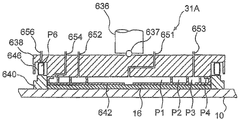
도 3은 톱 링(31A)의 구조를 모식적으로 나타낸 단면도이다. 톱 링(31A)은 톱 링 샤프트(636)의 하단(下端)에 자재(自在) 이음매(637)를 개재하여 연결되어 있다. 자재 이음매(637)는 톱 링(31A)과 톱 링 샤프트(636)와의 서로의 틸팅을 허용하면서, 톱 링 샤프트(636)의 회전을 톱 링(31A)에 전달하는 볼 조인트이다. 톱 링(31A)은 대략 원반 형상의 톱 링 본체(638)와, 톱 링 본체(638)의 하부에 배치된 리테이너 링(640)을 구비하고 있다. 톱 링 본체(638)는 금속이나 세라믹스 등의 강도 및 강성이 높은 재료로부터 형성되어 있다. 또, 리테이너 링(640)은 강성이 높은 수지재 또는 세라믹스 등으로부터 형성되어 있다. 또한, 리테이너 링(640)을 톱 링 본체(638)와 일체적으로 형성하는 것으로 해도 된다.3 is a cross-sectional view schematically showing the structure of the
톱 링 본체(638) 및 리테이너 링(640)의 내측에 형성된 공간 내에는, 반도체 웨이퍼(16)에 맞닿는 원형의 탄성 패드(642)와, 탄성막으로 이루어지는 환상의 가압 시트(643)와, 탄성 패드(642)를 보지하는 개략 원반 형상의 척킹 플레이트(644)가 수용되어 있다. 탄성 패드(642)의 상 주단(周端)부는 척킹 플레이트(644)에 보지되고, 탄성 패드(642)와 척킹 플레이트(644)와의 사이에는, 네 개의 압력실(에어 백)(P1, P2, P3, P4)이 마련되어 있다. 압력실(P1, P2, P3, P4)은 탄성 패드(642)와 척킹 플레이트(644)에 의해서 형성되어 있다. 압력실(P1, P2, P3, P4)에는 각각 유체로(651, 652, 653, 654)를 거쳐 가압 공기 등의 가압 유체가 공급되고, 또는 진공 배기가 되도록 되어 있다. 중앙의 압력실(P1)은 원형이고, 그 외의 압력실(P2, P3, P4)은 환상이다. 이들 압력실(P1, P2, P3, P4)은 동심 상으로 배열되어 있다.In the space formed inside the
압력실(P1, P2, P3, P4)의 내부 압력은 후술하는 압력 조정부에 의하여 서로 독립적으로 변화시키는 것이 가능하고, 이에 의해, 반도체 웨이퍼(16)의 네 개의 영역, 즉, 중앙부, 내측 중간부, 외측 중간부, 및 주연(周緣)부에 대한 가압력을 독립적으로 조정할 수 있다. 또, 톱 링(31A)의 전체를 승강시킴으로써, 리테이너 링(640)을 소정의 가압력으로 연마 패드(10)에 가압할 수 있게 되어 있다. 척킹 플레이트(644)와 톱 링 본체(638)와의 사이에는 압력실(P5)이 형성되고, 이 압력실(P5)에는 유체로(655)를 거쳐 가압 유체가 공급되고, 또는 진공 배기가 되도록 되어 있다. 이에 의해, 척킹 플레이트(644) 및 탄성 패드(642) 전체가 상하 방향으로 움직일 수 있다.The internal pressures of the pressure chambers P1, P2, P3, and P4 can be changed independently of each other by a pressure adjusting unit, which will be described later, whereby four regions of the
반도체 웨이퍼(16)의 주단부는 리테이너 링(640)에 둘러싸여 있고, 연마 중에 반도체 웨이퍼(16)가 톱 링(31A)으로부터 튀어나오지 않도록 되어 있다. 압력실(P3)을 구성하는, 탄성 패드(642)의 부위에는 개구(도시 생략)가 형성되어 있고, 압력실(P3)에 진공을 형성함으로써 반도체 웨이퍼(16)가 톱 링(31A)에 흡착 보지되도록 되어 있다. 또, 이 압력실(P3)에 질소 가스, 건조 공기, 압축 공기 등을 공급함으로써, 반도체 웨이퍼(16)가 톱 링(31A)으로부터 릴리스되도록 되어 있다.The main end portion of the
도 4는 톱 링(31A)의 기타의 구조예를 모식적으로 나타내는 단면도이다. 이 예에서는, 척킹 플레이트는 마련되어 있지 않고, 탄성 패드(642)는 톱 링 본체(638)의 하면에 장착되어 있다. 또, 척킹 플레이트와 톱 링 본체(638)와의 사이의 압력실(P5)도 마련되어 있지 않다. 이를 대신하여, 리테이너 링(640)과 톱 링 본체(638)와의 사이에는 탄성 백(646)이 배치되어 있고, 그 탄성 백(646)의 내부에는 압력실(P6)이 형성되어 있다. 리테이너 링(640)은 톱 링 본체(638)에 대하여 상대적으로 상하 이동 가능하게 되어 있다. 압력실(P6)에는 유체로(656)가 연통(連通)되어 있고, 가압 공기 등의 가압 유체가 유체로(656)를 통하여 압력실(P6)에 공급되도록 되어 있다. 압력실(P6)의 내부 압력은 후술하는 압력 조정부에 의하여 조정 가능하게 되어 있다. 따라서, 반도체 웨이퍼(16)에 대한 가압력과는 독립적으로 리테이너 링(640)의 연마 패드(10)에 대한 가압력을 조정할 수 있다. 기타의 구성 및 동작은, 도 3에 나타내는 톱 링의 구성과 동일하다. 본 실시 형태에서는 도 3 또는 도 4 중 어느 타입의 톱 링을 이용할 수 있다.4 is a cross-sectional view schematically showing another structural example of the
도 4는 톱 링(31A)을 회전 및 요동시키는 기구를 설명하기 위한 단면도이다. 톱 링 샤프트(예를 들면, 스플라인 샤프트)(636)는 톱 링 헤드(660)에 회전 자유롭게 지지되어 있다. 또, 톱 링 샤프트(636)는 풀리(661, 662) 및 벨트(663)를 개재하여 모터(M1)의 회전축에 연결되어 있고, 모터(M1)에 의해서 톱 링 샤프트(636) 및 톱 링(31A)이 그 축심을 중심으로 회전한다. 이 모터(M1)는 톱 링 헤드(660)의 상부에 장착되어 있다. 또, 톱 링 헤드(660)와 톱 링 샤프트(636)는, 상하 구동원으로서의 에어 실린더(665)에 의해서 연결되어 있다. 이 에어 실린더(665)에 공급되는 에어(압축 기체)에 의하여 톱 링 샤프트(636) 및 톱 링(31A)이 일체로 상하 이동한다. 또한, 에어 실린더(665) 대신에, 볼 나사 및 서보 모터를 갖는 기구를 상하 구동원으로서 이용해도 된다.4 is a cross-sectional view for explaining a mechanism for rotating and swinging the
톱 링 헤드(660)는, 지지축(667)에 베어링(672)을 개재하여 회전 자유롭게 지지되어 있다. 이 지지축(667)은 고정축이고, 회전하지 않는 구조로 되어 있다. 톱 링 헤드(660)에는 모터(M2)가 설치되어 있고, 톱 링 헤드(660)와 모터(M2)와의 상대 위치는 고정이다. 이 모터(M2)의 회전축은, 도시하지 않은 회전 전달 기구(기어 등)를 개재하여 지지축(667)에 연결되어 있고, 모터(M2)를 회전시킴으로써, 톱 링 헤드(660)가 지지축(667)을 중심으로 하여 요동(스윙)하도록 되어 있다. 따라서, 톱 링 헤드(660)의 요동 운동에 의해, 그 선단(先端)에 지지된 톱 링(31A)은 회전 테이블(30A)의 상방의 연마 위치와 회전 테이블(30A)의 측방(側方)의 반송 위치와의 사이를 이동한다. 또한, 본 실시 형태에서는 톱 링(31A)을 요동시키는 요동 기구는 모터(M2)로 구성된다.The
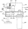
톱 링 샤프트(636)의 내부에는, 그 길이 방향으로 연장되는 관통 구멍(도시 생략)이 형성되어 있다. 상술한 톱 링(31A)의 유체로(651, 652, 653, 654, 655, 656)는, 이 관통 구멍을 통과하여, 톱 링 샤프트(636)의 상단(上端)에 마련되어 있는 회전 이음매(669)에 접속되어 있다. 이 회전 이음매(669)를 개재하여 톱 링(31A)에 가압 기체(클린 에어)나 질소 가스 등의 유체가 공급되고, 또, 톱 링(31A)으로부터 기체가 진공 배기된다. 회전 이음매(669)에는, 상기 유체 통로(651, 652, 653, 654, 655, 656)에 연통하는 복수의 유체관(670)이 접속되고, 이들 유체관(670)은 압력 조정부(675)에 접속되어 있다. 또, 에어 실린더(665)에 가압 공기를 공급하는 유체관(671)도 압력 조정부(675)에 접속되어 있다.A through hole (not shown) extending in the longitudinal direction is formed inside the
압력 조정부(675)는, 톱 링(31A)에 공급되는 유체의 압력을 조정하는 전공(電空) 레귤레이터나, 유체관(670, 671)에 접속되는 배관, 이들 배관에 마련된 에어 오퍼레이트 밸브, 이들 에어 오퍼레이트 밸브의 작동원이 되는 에어의 압력을 조정하는 전공 레귤레이터, 톱 링(31A)에 진공을 형성하는 이젝터 등을 갖고 있고, 이들이 집합하여 하나의 블록(유닛)을 구성하고 있다. 압력 조정부(675)는 톱 링 헤드(660)의 상부에 고정되어 있다. 톱 링(31A)의 압력실(P1, P2, P3, P4, P5)에 공급되는 가압 기체나, 에어 실린더(665)에 공급되는 가압 공기의 압력은, 이 압력 조정부(675)의 전공 레귤레이터에 의해서 조정된다. 마찬가지로, 압력 조정부(675)의 이젝터에 의해서 톱 링(31A)의 에어백(P1, P2, P3, P4) 내나, 척킹 플레이트(644)와 톱 링 본체(638)의 사이의 압력실(P5) 내에 진공이 형성된다.The
이와 같이, 압력 조정 기기인 전공 레귤레이터나 밸브가 톱 링(31A)의 근처에 설치되어 있으므로, 톱 링(31A) 내의 압력의 제어성이 향상된다. 보다 구체적으로는, 전공 레귤레이터와 압력실(P1, P2, P3, P4, P5)과의 거리가 짧으므로, 제어부(65)로부터의 압력 변경 지령에 대한 응답성이 향상한다. 마찬가지로, 진공원인 이젝터도 톱 링(31A)의 근처에 설치되어 있으므로, 톱 링(31A) 내에 진공을 형성할 때의 응답성이 향상한다. 또, 압력 조정부(675)의 이면을, 전장 기기의 장착용 대좌(臺座)로서 이용할 수 있어, 종래에 필요했던 장착용의 프레임을 필요없게 할 수 있다.In this way, since a pneumatic regulator or a valve as a pressure regulating device is provided near the
톱 링 헤드(660), 톱 링(31A), 압력 조정부(675), 톱 링 샤프트(636), 모터(M1), 모터(M2), 에어 실린더(665)는, 하나의 모듈(이하, 톱 링 어셈블리라고 함)로서 구성되어 있다. 즉, 톱 링 샤프트(636), 모터(M1), 모터(M2), 압력 조정부(675), 에어 실린더(665)는 톱 링 헤드(660)에 장착되어 있다. 톱 링 헤드(660)는, 지지축(667)으로부터 떼어낼 수 있도록 구성되어 있다. 따라서, 톱 링 헤드(660)와 지지축(667)을 분리함으로써, 톱 링 어셈블리를 기판 처리 장치로부터 떼어낼 수 있다. 이와 같은 구성에 의하면, 지지축(667)이나 톱 링 헤드(660) 등의 메인티넌스성을 향상시킬 수 있다. 예를 들면, 베어링(672)으로부터 이음(異音)이 발생하였을 때에, 베어링(672)을 용이하게 교환할 수 있고, 또, 모터(M2)나 회전 전달 기구(감속기)를 교환할 때에, 인접하는 기기를 떼어낼 필요도 없다.The
도 6은 회전 테이블(30A)의 내부 구조를 모식적으로 나타내는 단면도이다. 도 6에 나타내는 바와 같이, 회전 테이블(30A)의 내부에는, 반도체 웨이퍼(16)의 막의 상태를 검지하는 센서(676)가 매설되어 있다. 이 예에서는, 센서(676)로서 와전류 센서가 이용되고 있다. 센서(676)의 신호는 제어부(65)에 송신되고, 제어부(65)에 의해서 막두께를 나타내는 모니터링 신호가 생성되도록 되어 있다. 이 모니터링 신호(및 센서 신호)의 값은 막두께 자체를 나타내는 것은 아니지만, 모니터링 신호의 값은 막두께에 따라서 변화한다. 따라서, 모니터링 신호는 반도체 웨이퍼(16)의 막두께를 나타내는 신호라고 할 수 있다.6 is a cross-sectional view schematically showing the internal structure of the rotary table 30A. As shown in FIG. 6, inside the rotary table 30A, a
제어부(65)는, 모니터링 신호에 기초하여 각각의 압력실(P1, P2, P3, P4)의 내부 압력을 결정하고, 결정된 내부 압력이 각각의 압력실(P1, P2, P3, P4)에 형성되도록 압력 조정부(675)에 지령을 내도록 되어 있다. 제어부(65)는, 모니터링 신호에 기초하여 각각의 압력실(P1, P2, P3, P4)의 내부 압력을 조작하는 압력 제어부로서, 및 연마 종점을 검지하는 종점 검지부로서 기능한다.The
센서(676)는, 제 1 연마 유닛(3A)과 마찬가지로, 제 2 연마 유닛(3B), 제 3 연마 유닛(3C) 및 제 4 연마 유닛(3D)의 회전 테이블에도 마련되어 있다. 제어부(65)는, 각각의 연마 유닛(3A∼3D)의 센서(76)로부터 보내어져 오는 신호로부터 모니터링 신호를 생성하고, 각각의 연마 유닛(3A∼3D)에서의 반도체 웨이퍼의 연마의 진척을 감시한다. 복수의 반도체 웨이퍼가 연마 유닛(3A∼3D)에 의해 연마되어 있는 경우, 제어부(5)는, 반도체 웨이퍼의 막두께를 나타내는 모니터링 신호를 연마 중에 감시하고, 그들 모니터링 신호에 기초하여, 연마 유닛(3A∼3D)에서의 연마 시간이 대략 동일하게 되도록 톱 링(31A∼31D)의 가압력을 제어한다. 이와 같이 연마 중의 톱 링(31A∼31D)의 가압력을 모니터링 신호에 기초하여 조정함으로써, 연마 유닛(3A∼3D)에서의 연마 시간을 평준화할 수 있다.Like the
반도체 웨이퍼(16)는 제 1 연마 유닛(3A), 제 2 연마 유닛(3B), 제 3 연마 유닛(3C), 제 4 연마 유닛(3D) 중 어느 것에 의해 연마되어도 되고, 또는 이들 연마 유닛(3A∼3D)으로부터 미리 선택된 복수의 연마 유닛에 의해 연속적으로 연마되어도 된다. 예를 들면, 반도체 웨이퍼(16)를 제 1 연마 유닛(3A)→제 2 연마 유닛(3B)의 순서로 연마해도 되고, 또는 반도체 웨이퍼(16)를 제 3 연마 유닛(3C)→제 4 연마 유닛(3D)의 순서로 연마해도 된다. 또한, 반도체 웨이퍼(16)를 제 1 연마 유닛(3A)→제 2 연마 유닛(3B)→제 3 연마 유닛(3C)→제 4 연마 유닛(3D)의 순서로 연마해도 된다. 어느 경우이더라도, 연마 유닛(3A∼3D)의 모든 연마 시간을 평준화함으로써, 스루풋을 향상시킬 수 있다.The
와전류 센서는, 반도체 웨이퍼의 막이 금속막인 경우에 적절하게 이용된다. 반도체 웨이퍼의 막이 산화막 등의 광투과성을 갖는 막인 경우에는, 센서(76)로서 광학식 센서를 이용할 수 있다. 또는, 센서(76)로서 마이크로파 센서를 이용해도 된다. 마이크로파 센서는, 금속막 및 비금속막의 어느 경우에도 이용할 수 있다. 이하에, 광학식 센서 및 마이크로파 센서의 일례에 대하여 설명한다.The eddy current sensor is suitably used when the film of the semiconductor wafer is a metal film. When the film of the semiconductor wafer is a film having light transmittance such as an oxide film, an optical sensor can be used as the sensor 76. Alternatively, a microwave sensor may be used as the sensor 76. The microwave sensor can be used for both metal films and non-metal films. Below, an example of an optical sensor and a microwave sensor is demonstrated.
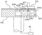
도 7은 광학식 센서를 구비한 회전 테이블을 나타내는 모식도이다. 도 7에 나타내는 바와 같이, 회전 테이블(30A)의 내부에, 반도체 웨이퍼(16)의 막의 상태를 검지하는 광학식 센서(676)가 매설되어 있다. 이 센서(676)는, 반도체 웨이퍼(16)에 광을 조사하고, 반도체 웨이퍼(16)로부터의 반사광의 강도(반사 강도 또는 반사율)로부터 반도체 웨이퍼(16)의 막의 상태(막두께 등)를 검지한다.7 is a schematic view showing a rotating table equipped with an optical sensor. As shown in FIG. 7, inside the rotary table 30A, an
또, 연마 패드(10)에는, 센서(676)로부터의 광을 투과시키기 위한 투광부(677)가 장착되어 있다. 이 투광부(677)는 투과율이 높은 재질로 형성되어 있고, 예를 들면, 무발포 폴리우레탄 등에 의해 형성된다. 또는, 연마 패드(10)에 관통 구멍을 마련하고, 이 관통 구멍이 반도체 웨이퍼(16)에 막히는 동안 하방(下方)으로부터 투명액을 흐르게 함으로써, 투광부(677)를 구성해도 된다. 투광부(677)는 톱 링(31A)에 보지된 반도체 웨이퍼(16)의 중심을 통과하는 위치에 배치된다.In addition, the
센서(676)는, 도 7에 나타내는 바와 같이, 광원(678a)과, 광원(678a)으로부터의 광을 반도체 웨이퍼(16)의 피연마면에 조사하는 발광부로서의 발광 광파이버(678b)와, 피연마면으로부터의 반사광을 수광하는 수광부로서의 수광 광파이버(678c)와, 수광 광파이버(678c)에 의해 수광된 광을 분광하는 분광기 및 이 분광기에 의하여 분광된 광을 전기적 정보로서 축적하는 복수의 수광 소자를 내부에 갖는 분광기 유닛(678d)과, 광원(678a)의 점등 및 소등이나 분광기 유닛(678d) 내의 수광 소자의 판독 개시의 타이밍 등의 제어를 행하는 동작 제어부(678e)와, 동작 제어부(678e)에 전력을 공급하는 전원(678f)을 구비하고 있다. 또한, 광원(678a) 및 분광기 유닛(678d)에는, 동작 제어부(678e)를 거쳐 전력이 공급된다.As shown in FIG. 7, the
발광 광파이버(678b)의 발광단(端)과 수광 광파이버(678c)의 수광단은, 반도체 웨이퍼(16)의 피연마면에 대하여 대략 수직이 되도록 구성되어 있다. 분광기 유닛(678d) 내의 수광 소자로서는, 예를 들면, 128 소자의 포토 다이오드 어레이를 이용할 수 있다. 분광기 유닛(678d)은 동작 제어부(678e)에 접속되어 있다. 분광기 유닛(678d) 내의 수광 소자로부터의 정보는, 동작 제어부(678e)에 보내어지고, 이 정보에 기초하여 반사광의 스펙트럼 데이터가 생성된다. 즉, 동작 제어부(678e)는, 수광 소자에 축적된 전기적 정보를 판독하여 반사광의 스펙트럼 데이터를 생성한다. 이 스펙트럼 데이터는, 파장에 따라서 분해된 반사광의 강도를 나타내고, 막두께에 의해서 변화한다.The light-emitting end of the light-emitting
동작 제어부(678e)는, 상술한 제어부(65)에 접속되어 있다. 이와 같이 하여, 동작 제어부(678e)에서 생성된 스펙트럼 데이터는, 제어부(65)에 송신된다. 제어부(65)에서는, 동작 제어부(678e)로부터 수신한 스펙트럼 데이터에 기초하여, 반도체 웨이퍼(16)의 막두께에 관련지어진 특성값을 산출하여, 이를 모니터링 신호로서 사용한다.The
도 8은 마이크로파 센서를 구비한 회전 테이블을 나타내는 모식도이다. 센서(676)는, 마이크로파를 반도체 웨이퍼(16)의 피연마면을 향하여 조사하는 안테나(680a)와, 안테나(680a)에 마이크로파를 공급하는 센서 본체(680b)와, 안테나(680a)와 센서 본체(680b)를 접속하는 도파관(681)을 구비하고 있다. 안테나(680a)는 회전 테이블(30A)에 매설되어 있고, 톱 링(31A)에 보지된 반도체 웨이퍼(16)의 중심 위치에 대향하도록 배치되어 있다.8 is a schematic view showing a rotating table equipped with a microwave sensor. The
센서 본체(680b)는, 마이크로파를 생성하여 안테나(680a)에 마이크로파를 공급하는 마이크로파원(680c)과, 마이크로파원(680c)에 의하여 생성된 마이크로파(입사파)와 반도체 웨이퍼(16)의 표면으로부터 반사한 마이크로파(반사파)를 분리시키는 분리기(680d)와, 분리기(680d)에 의하여 분리된 반사파를 수신하여 반사파의 진폭 및 위상을 검출하는 검출부(680e)를 구비하고 있다. 또한, 분리기(680d)로서는 방향성 결합기가 적절하게 이용된다.The
안테나(680a)는 도파관(681)을 거쳐 분리기(680d)에 접속되어 있다. 마이크로파원(680c)은 분리기(680d)에 접속되고, 마이크로파원(680c)에 의하여 생성된 마이크로파는, 분리기(680d) 및 도파관(681)을 거쳐 안테나(680a)에 공급된다. 마이크로파는 안테나(680a)로부터 반도체 웨이퍼(16)를 향하여 조사되고, 연마 패드(610)을 투과(관통)하여 반도체 웨이퍼(16)에 도달한다. 반도체 웨이퍼(16)로부터의 반사파는 다시 연마 패드(10)를 투과한 후, 안테나(680a)에 의하여 수신된다.The
반사파는 안테나(680a)로부터 도파관(681)을 거쳐 분리기(680d)에 보내어지고, 분리기(680d)에 의해서 입사파와 반사파가 분리된다. 분리기(680d)에 의하여 분리된 반사파는 검출부(680e)에 송신된다. 검출부(680e)에서는 반사파의 진폭 및 위상이 검출된다. 반사파의 진폭은 전력(dbm 또는 W) 또는 전압(V)으로서 검출되고, 반사파의 위상은 검출부(680e)에 내장된 위상 계측기(도시 생략)에 의하여 검출된다. 검출부(680e)에 의해서 검출된 반사파의 진폭 및 위상은 제어부(65)에 보내어지고, 여기서 반사파의 진폭 및 위상에 기초하여 반도체 웨이퍼(16)의 금속막이나 비금속막 등의 막두께가 해석된다. 해석된 값은, 모니터링 신호로서 제어부(65)에 의하여 감시된다.The reflected wave is sent from the
도 1에 나타내는 바와 같이, 드레서(33A)는 드레서 아암(685)과, 드레서 아암(685)의 선단에 회전 자유롭게 장착된 드레싱 부재(686)와, 드레서 아암(685)의 타단(他端)에 연결되는 요동축(688)과, 요동축(688)을 중심으로 드레서 아암(685)을 요동(스윙)시키는 구동 기구로서의 모터를 구비하고 있다. 드레싱 부재(686)는 원형의 드레싱면을 갖고 있고, 드레싱면에는 경질(硬質)인 입자가 고정되어 있다. 이 경질인 입자로서는, 다이아몬드 입자나 세라믹 입자 등을 들 수 있다. 드레서 아암(685) 내에는, 도시하지 않은 모터가 내장되어 있고, 이 모터에 의해서 드레싱 부재(686)가 회전하도록 되어 있다. 요동축(688)은 도시하지 않은 승강 기구에 연결되어 있고, 이 승강 기구에 의하여 드레서 아암(685)이 하강함으로써 드레싱 부재(686)가 연마 패드(10)의 연마면을 가압하도록 되어 있다.As shown in FIG. 1, the
도 1에 나타내는 아토마이저(34A)는, 하부에 1 또는 복수의 분사 구멍을 갖는 아암(690)과, 이 아암(690)에 연결된 유체 유로와, 아암(690)을 지지하는 요동축(694)을 구비하고 있다. 아암(690)의 하부에는 복수의 분사 구멍이 등간격으로 형성되어 있다.The
이용되는 유체의 예로서는, 액체(예를 들면, 순수), 또는 액체와 기체의 혼합 유체(예를 들면, 순수와 질소 가스의 혼합 유체) 등을 들 수 있다. 유체 유로는 아암(690)의 분사 구멍에 연통해 있고, 유체는 안개 형상으로 되어 분사 구멍으로부터 연마 패드(10)의 연마면에 분사된다.Examples of the fluid used include a liquid (for example, pure water) or a mixed fluid for a liquid and gas (for example, a mixed fluid for pure water and nitrogen gas). The fluid flow path communicates with the injection hole of the
아암(690)은, 요동축(694)을 중심으로 하여 세정 위치와 퇴피 위치와의 사이에서 선회 가능하게 되어 있다. 아암(690)의 가동 각도는 약 90°이다. 통상, 아암(690)은 세정 위치에 있고, 도 1에 나타내는 바와 같이, 연마 패드(10)의 연마면의 직경 방향을 따라서 배치되어 있다. 연마 패드(10)의 교환 등의 메인티넌스 시에는, 아암(690)은 수동에 의하여 퇴피 위치로 이동한다. 따라서, 메인티넌스 시에 아암(690)을 떼어낼 필요가 없어, 메인티넌스성을 향상시킬 수 있다. 또한, 회전 기구를 요동축(694)에 연결하고, 이 회전 기구에 의하여 아암(690)을 선회시켜도 된다.The
이 아토마이저(34A)를 마련하는 목적은, 연마 패드(10)의 연마면에 잔류하는 연마 부스러기나 숫돌 입자 등을 고압의 유체에 의하여 씻어 흐르게 하는 것이다. 아토마이저(34A)의 유체압에 의한 연마면의 정화와, 기계적 접촉인 드레서(33A)에 의한 연마면의 드레싱 작업에 의하여, 보다 바람직한 드레싱, 즉, 연마면의 재생을 달성할 수 있다. 통상은 접촉형의 드레서(다이아몬드 드레서 등)에 의한 드레싱 후에, 아토마이저에 의한 연마면의 재생을 행하는 경우가 많다.The purpose of providing the
다음으로, 반도체 웨이퍼를 반송하기 위한 반송 기구에 대하여, 도 1에 의하여 설명한다. 반송 기구는 리프터(11)와, 제 1 리니어 트랜스포터(66)와, 스윙 트랜스포터(12)와, 제 2 리니어 트랜스포터(67)와, 임시 거치대를 구비한다.Next, a transport mechanism for transporting the semiconductor wafer will be described with reference to FIG. 1. The transport mechanism includes a
리프터(11)는, 반송 로봇(22)으로부터 반도체 웨이퍼를 수취한다. 제 1 리니어 트랜스포터(66)는, 리프터(11)로부터 수취한 반도체 웨이퍼를, 제 1 반송 위치(TP1), 제 2 반송 위치(TP2), 제 3 반송 위치(TP3) 및 제 4 반송 위치(TP4), 의 사이에서 반송한다. 제 1 연마 유닛(3A) 및 제 2 연마 유닛(3B)은 제 1 리니어 트랜스포터(66)로부터 반도체 웨이퍼를 수취하여 연마한다. 제 1 연마 유닛(3A) 및 제 2 연마 유닛(3B)은 연마한 반도체 웨이퍼를 제 1 리니어 트랜스포터(66)로 넘겨준다.The
스윙 트랜스포터(12)는, 제 1 리니어 트랜스포터(66)와 제 2 리니어 트랜스포터(67)와의 사이에서 반도체 웨이퍼의 주고받음을 행한다. 제 2 리니어 트랜스포터(67)는, 스윙 트랜스포터(12)로부터 수취한 반도체 웨이퍼를, 제 5 반송 위치(TP5), 제 6 반송 위치(TP6) 및 제 7 반송 위치(TP7), 의 사이에서 반송한다. 제 3 연마 유닛(3C) 및 제 4 연마 유닛(3D)은, 제 2 리니어 트랜스포터(67)로부터 반도체 웨이퍼를 수취하여 연마한다. 제 3 연마 유닛(3C) 및 제 4 연마 유닛(3D)은, 연마한 반도체 웨이퍼를 제 2 리니어 트랜스포터(67)로 넘겨준다. 연마 유닛(3)에 의해서 연마 처리가 행해진 반도체 웨이퍼는 스윙 트랜스포터(12)에 의해서 임시 거치대에 놓여진다.The
도 1에 나타내는 바와 같이, 세정부(64)는 제 1 세정실(190)과 제 1 반송실(191)과 제 2 세정실(192)과 제 2 반송실(193)과 건조실(194)로 구획되어 있다. 제 1 세정실(190) 내에는, 세로 방향을 따라서 배열된 상측 일차 세정 모듈 및 하측 일차 세정 모듈이 배치되어 있다. 상측 일차 세정 모듈은 하측 일차 세정 모듈의 상방(上方)에 배치되어 있다. 마찬가지로, 제 2 세정실(192) 내에는, 세로 방향을 따라서 배열된 상측 이차 세정 모듈 및 하측 이차 세정 모듈이 배치되어 있다. 상측 이차 세정 모듈은 하측 이차 세정 모듈의 상방에 배치되어 있다. 일차 및 이차 세정 모듈은, 세정액을 이용하여 반도체 웨이퍼를 세정하는 세정기이다. 이들 일차 및 이차 세정 모듈은 수직 방향을 따라서 배열되어 있으므로, 풋 프린트 면적이 작다는 이점이 얻어진다.As shown in FIG. 1, the
상측 이차 세정 모듈과 하측 이차 세정 모듈과의 사이에는, 반도체 웨이퍼의 임시 거치대가 마련되어 있다. 건조실(194) 내에는, 세로 방향을 따라서 배열된 상측 건조 모듈 및 하측 건조 모듈이 배치되어 있다. 이들 상측 건조 모듈 및 하측 건조 모듈은 서로 격리되어 있다. 상측 건조 모듈 및 하측 건조 모듈의 상부에는 청정한 공기를 건조 모듈, 내에 각각 공급하는 필터 팬 유닛이 마련되어 있다. 상측 일차 세정 모듈, 하측 일차 세정 모듈, 상측 이차 세정 모듈, 하측 이차 세정 모듈, 임시 거치대, 상측 건조 모듈 및 하측 건조 모듈은 프레임에 볼트 등을 개재하여 고정되어 있다.A temporary holder for the semiconductor wafer is provided between the upper secondary cleaning module and the lower secondary cleaning module. In the drying
제 1 반송실(191)에는, 상하 이동 가능한 제 1 반송 로봇이 배치되고, 제 2 반송실(193)에는, 상하 이동 가능한 제 2 반송 로봇이 배치되어 있다. 제 1 반송 로봇 및 제 2 반송 로봇은, 세로 방향으로 연장되는 지지축에 각각 이동 자유롭게 지지되어 있다. 제 1 반송 로봇 및 제 2 반송 로봇은 그 내부에 모터 등의 구동 기구를 갖고 있고, 지지축을 따라서 상하로 이동 자유롭게 되어 있다. 제 1 반송 로봇은, 반송 로봇(22)과 마찬가지로, 상하 이단의 핸드를 갖고 있다. 제 1 반송 로봇은, 그 하측의 핸드가 상술한 임시 거치대에 액세스 가능한 위치에 배치되어 있다. 제 1 반송 로봇의 하측의 핸드가 임시 거치대에 액세스할 때에는, 격벽(1b)에 마련되어 있는 셔터가 개방되도록 되어 있다.In the
제 1 반송 로봇은, 임시 거치대, 상측 일차 세정 모듈, 하측 일차 세정 모듈, 임시 거치대, 상측 이차 세정 모듈, 하측 이차 세정 모듈의 사이에서 반도체 웨이퍼(16)를 반송하도록 동작한다. 세정 전의 반도체 웨이퍼(슬러리가 부착되어 있는 반도체 웨이퍼)를 반송할 때에는, 제 1 반송 로봇은, 하측의 핸드를 이용하여, 세정 후의 반도체 웨이퍼를 반송할 때에는 상측의 핸드를 이용한다. 제 2 반송 로봇은 상측 이차 세정 모듈, 하측 이차 세정 모듈, 임시 거치대, 상측 건조 모듈, 하측 건조 모듈의 사이에서 반도체 웨이퍼(16)를 반송하도록 동작한다. 제 2 반송 로봇은, 세정된 반도체 웨이퍼만을 반송하므로, 하나의 핸드만을 구비하고 있다. 도 1에 나타내는 반송 로봇(22)은, 그 상측의 핸드를 이용하여 상측 건조 모듈 또는 하측 건조 모듈로부터 반도체 웨이퍼를 취출하고, 그 반도체 웨이퍼를 웨이퍼 카세트로 되돌린다. 반송 로봇(22)의 상측 핸드가 건조 모듈에 액세스할 때에는, 격벽(1a)에 마련되어 있는 셔터(도시 생략)가 개방되도록 되어 있다.The first transfer robot operates to transport the
세정부(64)는, 2대의 일차 세정 모듈 및 2대의 이차 세정 모듈을 구비하고 있으므로, 복수의 반도체 웨이퍼를 병렬하여 세정하는 복수의 세정 라인을 구성할 수 있다. 「세정 라인」이란, 세정부(64)의 내부에 있어서, 하나의 반도체 웨이퍼가 복수의 세정 모듈에 의해서 세정될 때의 이동 경로를 말한다. 예를 들면, 하나의 반도체 웨이퍼를, 제 1 반송 로봇, 상측 일차 세정 모듈, 제 1 반송 로봇, 상측 이차 세정 모듈, 제 2 반송 로봇, 그리고 상측 건조 모듈의 순서로 반송하고, 이와 병렬하여, 기타의 반도체 웨이퍼를, 제 1 반송 로봇, 하측 일차 세정 모듈, 제 1 반송 로봇, 하측 이차 세정 모듈, 제 2 반송 로봇, 그리고 하측 건조 모듈의 순서로 반송할 수 있다. 이와 같이 두 개의 병렬하는 세정 라인에 의하여, 복수(전형적으로는 2매)의 반도체 웨이퍼를 대략 동시에 세정 및 건조할 수 있다.Since the
건조된 반도체 웨이퍼(16)는, 도 1에 나타내는 반송 로봇(22)에 의하여 건조 모듈로부터 취출되고, 웨이퍼 카세트로 되돌려진다. 이와 같이 하여, 연마, 세정 및 건조를 포함하는 일련의 처리가 반도체 웨이퍼에 대하여 행해진다. 상술과 같이 구성된 건조 모듈에 의하면, 반도체 웨이퍼(16)의 양면을 신속하고도 효과적으로 건조할 수 있고, 또, 정확하게 건조 처리의 종료 시점을 제어할 수 있다. 따라서, 건조 처리를 위한 처리 시간이 세정 프로세스 전체의 율속 공정으로 되는 일은 없다. 또, 세정부(4)에 형성되는 상술한 복수의 세정 라인에서의 처리 시간은 평준화할 수 있으므로, 프로세스 전체의 스루풋을 향상시킬 수 있다.The dried
본 실시 형태에 의하면, 반도체 웨이퍼를 연마 장치에 반입하였을 때(로드 전)에, 반도체 웨이퍼가 건조 상태에 있고, 연마와 세정이 종료 후, 언로드 전에, 반도체 웨이퍼가 건조 상태가 되어, 기판 카세트에 언로드된다. 건조 상태의 반도체 웨이퍼를 연마 장치로부터 카세트에 넣어, 취출하는 것이 가능하게 된다. 즉, 드라이 인/드라이 아웃이 가능하다.According to the present embodiment, when the semiconductor wafer is brought into the polishing apparatus (before loading), the semiconductor wafer is in a dry state, and after polishing and cleaning are finished, before unloading, the semiconductor wafer is in a dry state, and is transferred to the substrate cassette. Is unloaded. The dried semiconductor wafer can be placed in a cassette from a polishing apparatus and taken out. That is, dry in / dry out is possible.
임시 거치대에 놓여진 반도체 웨이퍼는, 제 1 반송실(191)을 거쳐 제 1 세정실(190) 또는 제 2 세정실(192)로 반송된다. 반도체 웨이퍼는 제 1 세정실(190) 또는 제 2 세정실(192)에 있어서 세정 처리된다. 제 1 세정실(190) 또는 제 2 세정실(192)에 있어서 세정 처리된 반도체 웨이퍼는, 제 2 반송실(193)을 거쳐 건조실(194)로 반송된다. 반도체 웨이퍼는 건조실(194)에 있어서 건조 처리된다. 건조 처리된 반도체 웨이퍼는 반송 로봇(22)에 의해서 건조실(194)로부터 취출되어 카세트로 되돌려진다.The semiconductor wafer placed on the temporary cradle is transferred to the
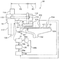
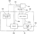
도 9는 본 발명의 일 실시 형태에 관련된 연마 유닛(연마 장치)의 전체 구성을 나타내는 개략도이다. 도 9에 나타내는 바와 같이, 연마 장치는 회전 테이블(30A)과, 연마 대상물인 반도체 웨이퍼(16) 등의 기판을 보지하여 회전 테이블 상의 연마면에 가압하는 톱 링(31A)(보지부)을 구비하고 있다.9 is a schematic view showing the overall configuration of a polishing unit (polishing apparatus) according to an embodiment of the present invention. As shown in Fig. 9, the polishing apparatus includes a rotating table 30A and a
제 1 연마 유닛(3A)은 연마 패드(10)와, 연마 패드(10)에 대향하여 배치되는 반도체 웨이퍼(16)와의 사이에서 연마를 행하기 위한 연마 유닛이다. 제 1 연마 유닛(3A)은, 연마 패드(10)를 보지하기 위한 회전 테이블(30A)과, 반도체 웨이퍼(16)를 보지하기 위한 톱 링(31A)을 갖는다. 제 1 연마 유닛(3A)은, 톱 링(31A)을 보지하기 위한 요동 아암(110)과, 요동 아암(110)을 요동하기 위한 요동축 모터(14)(아암 구동부)와, 요동축 모터(14)에, 구동 전력을 공급하는 드라이버(18)를 갖는다. 또한, 제 1 연마 유닛(3A)은, 요동 아암(110)에 가해지는 아암 토오크를 검지하는 아암 토오크 검지부(26)와, 아암 토오크 검지부(26)가 검지한 아암 토오크(26a)에 기초하여, 연마의 종료를 나타내는 연마 종점을 검출하는 종점 검출부(28)를 갖는다.The
도 9 이하에 의하여 설명하는 본 실시 형태에 의하면, 막두께의 측정 정밀도를 개선한 연마 유닛(3A)을 제공할 수 있다. 또, 본 실시 형태의 연마 유닛(3A)은, 막두께의 변화의 이상을 검지할 수 있다. 연마 유닛(3A)은 기계 학습 장치를 구비한다. 본 실시 형태에서는, 연마 종점 검출 수단으로서, 와전류 센서를 이용한 방법, 아암 토오크에 기초하는 방법, 회전 테이블 또는 톱 링을 회전 구동하는 구동부의 구동 부하를 검출하여 이용하는 방법 등이 가능하다. 본 실시 형태는, 톱 링을 요동 아암의 단부(端部)에 보지하는 방식에 있어서, 아암 토오크에 기초하여 연마 종점 검출을 행하는 것을 설명하지만, 회전 테이블 또는 톱 링을 회전 구동하는 구동부의 구동 부하를 모터 전류에 의하여 검출하여, 연마 종점 검출을 행하는 것도 마찬가지로 실시할 수 있다.According to this embodiment described with reference to FIG. 9 or less, it is possible to provide a
보지부와 요동 아암과 아암 구동부와 토오크 검지부는 세트를 구성하고, 동일한 구성을 갖는 세트가, 제 1 연마 유닛(3A), 제 2 연마 유닛(3B), 제 3 연마 유닛(3C), 제 4 연마 유닛(3D)의 각각에 마련되어 있다.The holding unit, the swinging arm, the arm driving unit and the torque detecting unit constitute a set, and the set having the same configuration includes the
회전 테이블(30A)은, 테이블축(102)을 개재하여 그 하방에 배치되는 구동부인 모터(도시 생략)에 연결되어 있고, 그 테이블축(102)을 중심으로 회전 가능하게 되어 있다. 회전 테이블(30A)의 상면에는 연마 패드(10)가 첩부되어 있고, 연마 패드(10)의 표면(101)이 반도체 웨이퍼(16)를 연마하는 연마면을 구성하고 있다. 회전 테이블(30A)의 상방에는 연마액 공급 노즐(도시하지 않음)이 설치되어 있고, 연마액 공급 노즐에 의해서 회전 테이블(30A) 상의 연마 패드(10)에 연마액(Q)이 공급된다. 도 9에 나타내는 바와 같이, 회전 테이블(30A)의 내부에는, 반도체 웨이퍼(16) 내에 와전류를 생성하여, 당해 와전류를 검출함으로써 연마 종점을 검지할 수 있는 와전류 센서(50)가 매설되어 있어도 된다.The rotating table 30A is connected to a motor (not shown) that is a driving unit disposed below the
톱 링(31A)은, 반도체 웨이퍼(16)를 연마면(101)에 대하여 가압하는 톱 링 본체(24)와, 반도체 웨이퍼(16)의 외주연을 보지하여 반도체 웨이퍼(16)가 톱 링으로부터 튀어나오지 않도록 하는 리테이너 링(23)으로 구성되어 있다.The
톱 링(31A)은, 톱 링 샤프트(111)에 접속되어 있다. 톱 링 샤프트(111)는, 도시하지 않은 상하 이동 기구에 의하여 요동 아암(110)에 대하여 상하 이동한다. 톱 링 샤프트(111)의 상하 이동에 의하여, 요동 아암(110)에 대하여 톱 링(31A)의 전체를 승강시켜 위치결정한다.The
또, 톱 링 샤프트(111)는 키(도시 생략)를 개재하여 회전통(112)에 연결되어 있다. 이 회전통(112)은 그 외주부에 타이밍 풀리(113)를 구비하고 있다. 요동 아암(110)에는 톱 링용 모터(114)가 고정되어 있다. 상기 타이밍 풀리(113)은, 타이밍 벨트(115)를 개재하여 톱 링용 모터(114)에 마련된 타이밍 풀리(116)에 접속되어 있다. 톱링용 모터(114)가 회전하면, 타이밍 풀리(116), 타이밍 벨트(115), 및 타이밍 풀리(113)를 개재하여 회전통(112) 및 톱 링 샤프트(111)가 일체로 회전하고, 톱 링(31A)이 회전한다.In addition, the
요동 아암(110)은, 요동축 모터(14)의 회전축에 접속되어 있다. 요동축 모터(14)는 요동 아암 샤프트(117)에 고정되어 있다. 따라서, 요동 아암(110)은 요동 아암 샤프트(117)에 대하여 회전 가능하게 지지되어 있다.The swinging
톱 링(31A)은, 그 하면에 반도체 웨이퍼(16) 등의 기판을 보지할 수 있다. 요동 아암(110)은, 요동 아암 샤프트(117)를 중심으로 하여, 선회 가능하다. 하면에 반도체 웨이퍼(16)를 보지한 톱 링(31A)은, 요동 아암(110)의 선회에 의하여, 반도체 웨이퍼(16)의 수취 위치로부터 회전 테이블(30A)의 상방으로 이동된다. 그리고, 톱 링(31A)을 하강시켜, 반도체 웨이퍼(16)를 연마 패드(10)의 표면(연마면)(101)에 가압한다. 이 때, 톱 링(31A) 및 회전 테이블(30A)을 각각 회전시킨다. 동시에, 회전 테이블(30A)의 상방에 마련된 연마액 공급 노즐로부터 연마 패드(10) 상에 연마액을 공급한다. 이와 같이, 반도체 웨이퍼(16)를 연마 패드(10)의 연마면(101)에 슬라이딩 접촉시켜, 반도체 웨이퍼(16)의 표면을 연마한다.The
제 1 연마 유닛(3A)은, 회전 테이블(30A)을 회전 구동하는 테이블 구동부(도시하지 않음)를 갖는다. 제 1 연마 유닛(3A)은, 회전 테이블(30A)에 가해지는 테이블 토오크를 검지하는 테이블 토오크 검지부(도시하지 않음)를 가져도 된다. 테이블 토오크 검지부는, 회전 모터인 테이블 구동부의 전류로부터 테이블 토오크를 검지할 수 있다. 종점 검출부(28)는, 아암 토오크 검지부(26)가 검지한 아암 토오크(26a)만으로부터 연마의 종료를 나타내는 연마 종점을 검출해도 되고, 테이블 토오크 검지부가 검지한 테이블 토오크도 고려하여, 연마의 종료를 나타내는 연마 종점을 검출해도 된다.The
도 9에 있어서는, 요동 아암(110)의, 요동축 모터(14)에의 접속부에 있어서, 아암 토오크 검지부(26)는, 요동 아암(110)에 가해지는 아암 토오크(26a)를 검지한다. 구체적으로는, 아암 구동부는, 요동 아암(110)을 회전시키는 요동축 모터(회전 모터)(14)이고, 아암 토오크 검지부(26)는, 요동축 모터(14)의 전류값으로부터, 요동 아암(110)에 가해지는 아암 토오크(26a)를 검지한다. 요동축 모터(14)의 전류값은, 요동 아암(110)의, 요동축 모터(14)에의 접속부에 있어서의 아암 토오크에 의존하는 양이다. 요동축 모터(14)의 전류값은, 본 실시 형태에서는, 드라이버(18)로부터 요동축 모터(14)에 공급되는 전류값(18b), 또는, 드라이버(18) 내에서 생성되는 후술하는 전류 지령(18a)이다.In FIG. 9, in the connecting portion of the swinging
드라이버(18)는, 제어부(65)로부터, 요동 아암(110)의 위치에 관한 위치 지령(65a)을 입력 받는다. 위치 지령(65a)은, 요동 아암 샤프트(117)에 대한 요동 아암(110)의 회전 각도에 상당하는 데이터이다. 드라이버(18)는, 또, 요동축 모터(14)에 내장하여 장착된 엔코더(도시 생략)로부터, 요동 아암 샤프트(117)의 회전 각도를 입력 받는다.The
전류 지령(18a)은, 요동축 모터(14)의 전류값에 의존하는 양이고, 아암 토오크에 의존하는 양이다. 아암 토오크 검지부(26)는, 전류 지령(18a)에 대하여, AD 변환, 증폭, 정류, 실효값 변환 등의 처리 중 적어도 하나의 처리를 한 후에, 종점 검출부(28)에, 아암 토오크(26a)로서 출력한다.The
전류 지령(18a)으로부터 전류값이 생성된다. 전류값은, 요동축 모터(14)의 전류값 자체임과 함께, 아암 토오크에 의존하는 양이다. 아암 토오크 검지부(26)는, 전류값으로부터, 요동 아암(110)에 가해지는 아암 토오크를 검지해도 된다. 아암 토오크 검지부(26)는, 전류값을 검출할 때에, 홀 센서 등의 전류 센서를 이용할 수 있다.A current value is generated from the
회전 테이블을 회전 구동하기 위한 모터(M3)(제 1 전동 모터, 도 2를 참조), 톱 링(31A)을 회전 구동하기 위한 모터(M1)(제 2 전동 모터, 도 5를 참조), 및 요동 아암을 요동하기 위한 모터(M2)(제 3 전동 모터, 도 5를 참조) 중 하나의 전동 모터의 전류값을 검출할 수 있다. 전류 지령(18a)이나 전류값과, 막두께와의 대응 관계로부터, 막두께를 종점 검출부(28)의 막두께 산출부(830)(도 10 참조)는 구할 수 있다. 전류 지령(18a)이나 전류값과, 막두께와의 대응 관계는, 예를 들면, 연마 공정의 개시 전에 구해 두고, 막두께 산출부(830) 내에 기억해 둘 수 있다.Motor M3 for rotationally driving the rotary table (first electric motor, see FIG. 2), motor M1 for rotationally driving the
다음으로, 도 10을 참조하여, 반도체 웨이퍼(16)(연마 대상물)의 막두께의 변화를 학습 가능한 종점 검출부(28)(기계 학습 장치)를 설명한다. 종점 검출부(28)는, 연마 유닛(3A)을 구성하는 기기의 상태에 관한 데이터, 및 반도체 웨이퍼(16)의 상태에 관한 데이터 중 적어도 하나를 포함하는 상태 변수를 취득 가능한 상태 취득부(846)와, 상태 변수에 기초하여 변화를 학습 가능한 학습부(848)를 구비한다. 연마 유닛(3A)을 구성하는 기기란, 예를 들면, 톱 링(31A), 회전 테이블(30A), 연마액 공급 노즐(32A), 드레서(33A), 아토마이저(34A) 등의 연마 유닛(3A)을 구성하는 기기이다.Next, with reference to FIG. 10, the endpoint detection part 28 (machine learning apparatus) which can learn the change of the film thickness of the semiconductor wafer 16 (object to be polished) is demonstrated. The end
연마 유닛(3A)을 구성하는 기기의 상태에 관한 데이터는, 기기의 배치에 관한 데이터, 기기의 동작 상태에 관한 데이터, 및 기기의 소모 상태에 관한 데이터 중 적어도 하나를 포함하고 있다.The data relating to the state of the equipment constituting the
반도체 웨이퍼(16)의 상태에 관한 데이터는, 반도체 웨이퍼(16)의 막두께를 검출 가능한 막두께 산출부(830)가 검출하는 데이터, 반도체 웨이퍼(16)의 온도를 검출 가능한 온도 센서(832)(온도 검출부)가 검출하는 데이터, 반도체 웨이퍼(16)에 가해지는 압력을 검출 가능한 제어부(65)(압력 검출부)가 검출하는 데이터, 및 연마 대상물의 특성에 관한 데이터 중 적어도 하나를 포함하고 있다. 반도체 웨이퍼(16)에 가해지는 압력에 관해서는, 제어부(65)는 예를 들면, 유체로(651, 652, 653, 654)에 마련된 압력 센서를 이용하여 압력을 검출 가능하다.Data relating to the state of the
이들 데이터는, 종점 검출부(28) 내의 상태 취득부(846)에 학습을 위하여 송신된다. 즉, 막두께 산출부(830)가 검출하는 데이터는, 신호(830a)로서, 막두께 산출부(830)로부터 상태 취득부(846)에 송신된다. 온도 센서(832)(온도 검출부)가 검출하는 데이터는, 온도 센서(832)로부터 상태 취득부(846)에 송신된다. 제어부(65)(압력 검출부)가 검출하는 데이터는, 신호(65b)로서 제어부(65)로부터 상태 취득부(846)에 송신된다.These data are transmitted to the
온도 검출부는, 온도 센서(832) 이외에, 반도체 웨이퍼(16)의 근방에 위치하는 연마 유닛(3A) 내의 회로의 저항 등으로서 반도체 웨이퍼(16)의 온도를 검출 가능한 저항 등이 포함된다. 온도 센서(832)는 반도체 웨이퍼(16)의 근방에 배치되고, 온도 센서(832)의 출력은, 종점 검출부(28) 내의 상태 취득부(846)에 송신된다.In addition to the
압력 검출부에는, 압력 센서, 반도체 웨이퍼(16)에 가하는 압력을 압력 지령으로서 압력 조정부(675)에 출력하는 제어부(65) 등이 포함된다. 제어부(65)가 압력 검출부인 경우, 제어부(65)가 검출하는 데이터는 압력 지령이어도 된다. 압력 지령은 압력 조정부(675)에 추가하여, 제어부(65)로부터 신호(65b)로서 상태 취득부(846)에 학습을 위하여 출력된다.The pressure detection unit includes a pressure sensor, a
기기의 배치에 관한 데이터는, 연마 대상물을 보지 가능한 톱 링(31A)의 위치에 관한 데이터, 연마 대상물을 연마하기 위한 연마 패드를 회전 가능한 회전 테이블(30A)의 위치에 관한 데이터, 톱 링(31A)을 보지하는 아암(110)의 위치에 관한 데이터, 및 연마 패드(10)의 드레싱을 행하는 것이 가능한 드레서(33A)의 위치에 관한 데이터 중 적어도 하나를 포함하고 있다.The data regarding the arrangement of the device includes data regarding the position of the
톱 링(31A)의 위치에 관한 데이터에는 예를 들면, 회전 테이블(30A)의 평면 상에 있어서의 위치(2차원 좌표값), 및 또는 톱 링(31A)의 회전 각도가 포함된다. 회전 테이블(30A)/아암(110)/드레서(33A)의 위치에 관한 데이터에는 예를 들면, 회전 테이블(30A/아암(110)/드레서(33A)의 회전 각도가 포함된다. 또한, 본 명세서에 있어서는 「/」는, 「및 또는」을 의미한다. 톱 링(31A)/회전 테이블(30A)/아암(110)/드레서(33A)의 위치에 관한 데이터에는 예를 들면, 회전 테이블(30A)의 평면 상에 있어서의 이들 기기의 상대적인 위치(2차원 좌표값)가 포함된다.The data regarding the position of the
기기의 배치에 관한 데이터에는, 반도체 웨이퍼(16)의 위치에 관한 데이터를 포함해도 된다. 반도체 웨이퍼(16)의 위치에 관한 데이터에는 예를 들면, 회전 테이블(30A)의 평면 상에 있어서의 위치(2차원 좌표값), 및 또는 반도체 웨이퍼(16)의 회전 각도가 포함된다. 반도체 웨이퍼(16)의 위치에 관한 데이터는 예를 들면, 상술의 톱 링(31A)/회전 테이블(30A)/아암(110)/드레서(33A)의 위치에 관한 데이터로부터 제어부(65)/상태 취득부(846)가 산출되어도 된다.The data regarding the arrangement of the devices may include data regarding the position of the
이들 데이터는 예를 들면, 제어부(65)로부터, 톱 링(31A)을 보지하는 아암, 회전 테이블(30A), 연마액 공급 노즐(32A)을 보지하는 아암, 및 드레서(33A)의 아암을 각각 구동하는 구동부에 출력되는 제어 지령이다. 제어 지령은 예를 들면, 회전 각도이다. 제어 지령은 구동부에 추가하여, 제어부(65)로부터 신호(65b)로서 상태 취득부(846)에 학습을 위하여 출력된다.These data include, for example, the arm holding the
기기의 동작 상태에 관한 데이터는, 톱 링(31A)의 회전수에 관한 데이터, 및 회전 테이블의 회전수에 관한 데이터 중 적어도 하나를 포함하고 있다. 이들 데이터는, 제어부(65)로부터, 톱 링(31A), 및 회전 테이블(30A)을 각각 회전 구동하는 구동부에 출력되는 제어 지령이다. 제어 지령은 예를 들면, 회전수이다. 제어 지령은 구동부에 추가하여, 제어부(65)로부터 신호(65b)로서 상태 취득부(846)에 학습을 위하여 출력된다.The data regarding the operating state of the device includes at least one of data regarding the number of revolutions of the
기기의 소모 상태에 관한 데이터는, 연마 장치를 구성하는 소모품의 사용 시간에 관한 데이터, 및 소모품의 소비량에 관한 데이터 중 적어도 하나를 포함하고 있다. 소모품은, 예를 들면, 연마 패드(10)/톱 링(31A)의 리테이너 링/멤브레인이다. 연마 패드(10)/톱 링(31A)의 리테이너 링/멤브레인의 사용 시간에 관한 데이터는 제어부(65)에 기억된다. 제어부(65)는 사용 시간에 관한 데이터를 상태 취득부(846)에 학습을 위하여 신호(65b)로서 출력한다. 연마 패드(10)의 소비량에 관한 데이터란, 연마 패드(10)의 소모량이다. 소모량은, 광학 센서(834)에 의해서 측정된다. 광학 센서(834)는 연마 패드(10)와 광학 센서(834)와의 거리를 측정함으로써, 소모량을 검출한다. 광학 센서(834)는 소모량에 관한 데이터를 상태 취득부(846)에 학습을 위하여 출력한다.The data related to the consumption state of the device includes at least one of data related to the usage time of the consumables constituting the polishing apparatus and data related to the consumption amount of the consumables. The consumable is, for example, a retainer ring / membrane of the
반도체 웨이퍼(16)의 특성에 관한 데이터는, 반도체 웨이퍼(16) 자체/반도체 웨이퍼(16) 상에 형성된 막/회로의 재질에 관한 데이터, 및 반도체 웨이퍼(16)가 연마 장치에 의해서 연마되기 전에 갖는 막두께 및 회로 패턴에 관한 데이터 중 적어도 하나를 포함하고 있다. 반도체 웨이퍼(16) 자체의 재질에 관한 데이터는, 재질이 구리, 알루미늄, Si, GaAs, SOI, 유리, SiC, 세라믹, 수지 기판 등이라는 것을 나타내는 데이터이다. 또는 반도체 웨이퍼(16)의 재질에 관한 데이터는, 이들 금속의 혼합비나, 산화막의 혼합비를 나타내는 데이터이다. 연마되기 전에 갖는 막두께 및 회로 패턴에 관한 데이터는, 예를 들면, 막두께를 나타내는 수치 데이터나, 회로 패턴을 분류한 데이터이다. 회로 패턴을 분류한 데이터란 예를 들면, 반도체 웨이퍼(16)에 포함되는 복수의 금속 성분의 비율을 나타내는 수치 데이터이다. 이들 데이터는, 사용자가 제어부(65)에 연마 개시 전에 입력한다. 제어부(65)는, 이들 데이터를 상태 취득부(846)에 신호(65c)로서 출력한다.The data relating to the characteristics of the
본 실시 형태에 있어서, 학습부(848)가 학습하기 위하여, 학습부(848)에 상태 취득부(846)를 거쳐 입력 가능한 데이터로서는, 이하와 같은 양에 관한 데이터의 일부 또는 전부가 가능하다. i) 요동 아암(110)이 연마시에 톱 링(31A)으로부터 받는 토오크, ii) 회전 테이블(30A), 톱 링(31A), 요동축 모터(14)의 모터 전류, iii) 연마 개시로부터의 경과 시간, iv) 회전 테이블(30A)의 회전수, v) 반도체 웨이퍼(16)에의 가압의 크기, vi) 연마 패드(10)의 온도, vii) 연마액 공급 노즐(32A)로부터 공급되는 슬러리의 유량, viii) 반도체 웨이퍼(16)의 막종(산화막, 도전성 막 등의 막의 종류), ix) 반도체 웨이퍼(16)의 막두께, x) 톱 링(31A)의 회전수, xi) 요동 아암(110)의 요동 속도, xii) 연마 패드(10)의 두께, xiii) 연마 패드(10) 등의 소모품의 사용 시간, xiv) 광학식 센서의 출력, xv) 와전류 센서의 출력, xvi) 마이크로파 센서의 출력, xvii) 초음파 센서의 출력, xviii) 진동(음파) 센서의 출력.In the present embodiment, in order for the
이들 데이터 중, 막두께의 변화의 학습을 위하여 바람직한 데이터로서는, 예를 들면, 이하의 7종류가 있다. 즉, i) 요동 아암(110)이 연마시에 톱 링(31A)으로부터 받는 토오크, iii) 연마 개시로부터의 경과 시간, iv) 회전 테이블(30A)의 회전수, v) 반도체 웨이퍼(16)에의 가압의 크기, vi) 연마 패드(10)의 온도, x) 톱 링(31A)의 회전수, xi) 요동 아암(110)의 요동 속도이다.Among these data, there are, for example, the following seven types of data that are preferable for learning the change in film thickness. That is, i) torque received from the
막두께의 변화의 학습을 위하여 특히 바람직한 데이터로서는, 예를 들면, 이하의 5종류가 있다. 즉, i) 요동 아암(110)이 연마시에 톱 링(31A)으로부터 받는 토오크, iii) 연마 개시로부터의 경과 시간, v) 반도체 웨이퍼(16)로의 가압의 크기, vi) 연마 패드(10)의 온도, xi) 요동 아암(110)의 요동 속도이다.The following five types of data are particularly preferable for learning the change in film thickness. That is, i) torque received from the
막두께의 변화의 학습을 위하여 더 바람직한 데이터로서는, 예를 들면, 이하의 3종류가 있다. 즉, i) 요동 아암(110)이 연마시에 톱 링(31A)으로부터 받는 토오크, iii) 연마 개시로부터의 경과 시간, vi) 연마 패드(10)의 온도이다. 또한, 이들 7종류, 5종류, 3종류의 데이터의 선택은, 이것에 한정되는 것이 아니라, 기타의 조합도 가능하다. 또, 종류의 수도 3, 5, 7에 한정되는 것이 아니라, 이들 수치보다 많아도 되고 적어도 된다. 막두께의 변화의 학습을 위한 바람직한 데이터는, 연마 조건이나 반도체 웨이퍼(16)의 상태 등으로부터 결정할 수 있다.More preferable data for learning the change in film thickness are, for example, the following three types. That is, i) the torque received by the swinging
종점 검출부(28)(기계 학습 장치)는, 연마 유닛(3A)의 이상의 유무 또는 이상의 정도를 판정한 판정 데이터를 취득하는 판정 데이터 취득부(844)를 구비한다. 학습부(848)는 상태 변수 및 판정 데이터의 조합에 기초하여 작성되는 데이터 세트에 기초하여, 반도체 웨이퍼(16)의 막두께의 변화를 학습한다.The end point detection unit 28 (machine learning device) includes a determination
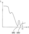
학습부(848)는 반도체 웨이퍼(16)의 막두께의 변화를 학습한 후에는, 변화를 예측 가능하다. 또, 학습부(848)는 반도체 웨이퍼(16)의 막두께의 변화를 학습하여, 변화가 정상인지 이상인지를 판단 가능하다.After learning the change in the film thickness of the
학습부(848)가 출력 가능한 데이터는, 막두께의 변화를 예측한 데이터(즉, 시계열 데이터로서의 막두께의 변화, 연마 종점 시각 등)와, 변화가 정상인지 이상인지를 판단한 데이터(예를 들면, 정상일 때는 「1」을 출력하고, 이상일 때는 「0」을 출력하는 등)에 한정되지 않는다. 학습부(848)가 출력 가능한 데이터로서는, 예를 들면, 이하가 있다.The data that can be output by the
i) 연마 종점 시각과, 그 때의 막두께 센서(토오크 센서, 전류 센서, 와전류 센서 등)의 예측 출력, ii) 연마 종점 시각과, 그 때의 막두께 센서의 예측 출력, 반도체 웨이퍼(16)에의 압력의 예측값, iii) 연마 종점 시각과, 그 때의 막두께 센서의 예측 출력, 반도체 웨이퍼(16)에의 압력의 예측값, 막두께의 예측 분포(예를 들면, 막두께의 균일성). 막두께 센서의 예측 출력, 반도체 웨이퍼(16)에의 압력의 예측값, 막두께의 예측 분포 등을 알 수 있으면, 제어부(65)는, 연마 조건(연마 파라미터)을 변경/갱신할 수 있고, 연마 조건의 제어를 최적화하는 것/연마 조건의 제어 정밀도를 향상할 수 있다. 예를 들면, 반도체 웨이퍼(16)에의 압력을 변경하는 것, 회전 테이블(30A)의 회전 속도를 변경하는 것 등을 제어부(65)는 행한다. 회전 속도를 느리게 하거나, 및 또는 압력을 낮게 하면, 연마 속도가 저하되어, 목표로 하는 막두께에 대하여 정밀도 좋게 막두께를 제어할 수 있다. 이와 같이, 학습부(848)는, 제어부(65)가 필요로 하는 압력 등의 임의의 제어 파라미터를 출력할 수 있다. 제어부(65)는, 연마 조건의 변경/갱신을, 학습부(848)가 그 입력 데이터를 취득한 현재 연마 중인 반도체 웨이퍼(16)에 대하여 행할 수 있는/제어부(65)는, 연마 조건의 변경/갱신을, 다음의 연마 공정에서 연마를 행하는 반도체 웨이퍼(16)에 대하여 행할 수 있다.i) Polishing end time and predicted output of film thickness sensor (torque sensor, current sensor, eddy current sensor, etc.) at that time, ii) Polished end time and predicted output of film thickness sensor at that time,
학습부(848)는, 연마 종점 시각에 있어서의 압력 등의 임의의 제어 파라미터의 예측값 이외에, 바람직한 연마를 위한 제어 파라미터의 목표값을 출력하는 것으로 해도 된다. 연마는, 막두께의 양호한 균일성과, 오차가 적은 최종 막두께를 목표로 하고 있다. 학습부(848)는, 이 목표에, 보다 적합하기 위한, 압력 등의 임의의 제어 파라미터의 목표값을 출력해도 된다. 제어부(65)는, 목표값에 따라서 연마 조건의 변경/갱신을 행하여, 연마 조건의 제어를 행할 수 있다. 목표값은 시간적으로 변화하는 것이어도 된다.The
학습부(848)의 출력은, 이하의 여러 가지 형태를 취할 수 있다. i) 학습부(848)는 수치를 출력한다. 예를 들면, 예측하는 압력 등을 수치의 형태로 출력한다. ii) 학습부(848)는 프로그램을 출력한다. 예를 들면, 압력 등을 시간 등의 변수로서 출력하는 등의 때에, 학습부(848)는, 압력 등의 시간 변화를 계산하는 프로그램을 출력해도 된다. iii) 학습부(848)는 계수를 출력한다. 예를 들면, 압력 등을 시간 등의 변수로서 표현하는 계산식의 계수나, 학습부(848)를 구성하는 뉴럴 네트워크의 가중 계수 등을 출력한다. 학습부(848)는, 이와 같이, 복수의 데이터를 출력할 수 있고, 또, 이들 중 하나의 데이터만을 출력하는 것으로 해도 된다.The output of the
또한, 학습부(848)에의 입력에 관해서도, 이미 서술한 복수의 데이터를 입력으로 할 수 있고, 또, 이들 중 하나의 데이터만을 입력으로 하는 것으로 해도 된다. 본 실시 형태에 있어서의 입력 데이터의 종류의 수와 출력 데이터의 종류의 수의 조합으로서는, i) 입력 데이터의 종류의 수가 1개이고, 출력 데이터의 종류의 수가 복수라는 조합, ii) 입력 데이터의 종류의 수가 복수이고, 출력 데이터의 종류의 수가 복수라는 조합, iii) 입력 데이터의 종류의 수가 복수이고, 출력 데이터의 종류의 수가 1개라는 조합의 어느 것도 가능하다.In addition, regarding the input to the
학습부(848)는, 제어부(65)가 필요로 하는 압력 등의 임의의 제어 파라미터 이외도 출력할 수 있다. 예를 들면, 학습부(848)를 구성하는 뉴럴 네트워크의 가중 계수 등의 학습부(848)를 구성하는 요소를 출력할 수 있다. 구성하는 요소를 출력함으로써, 학습부(848)를 개량할 수 있다.The
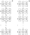
여기서, 학습의 개략과, 학습 후의 모델의 사용에 대하여, 도 11에 의하여 설명한다. 본 도면은 학습에 이용하는 데이터와, 알고리즘과, 학습필 모델의 사용예를 나타낸다. 학습에 이용하는 데이터, 즉, AI 프로그램의 입력 데이터(850)의 종류로서는, i) 각종 센서에 의하여 얻어진 데이터, ii) 반도체 웨이퍼(16)나 연마 패드(10) 등의 재료 등에 관한 데이터, iii) 센서 데이터 등을 화상화한 화상 데이터, iv) 센서 데이터 등을 학습에 적합하도록 적어도 부분적으로 가공한 가공 데이터, v) 연마 유닛(3A)에 입력되는 제어값 등의 연마를 위한 입력 파라미터, vi) i부터 v까지의 데이터에 관하여 과거에 작성된 또는 기타의 연마 유닛(3A)에 관하여 작성된 데이터베이스, vii) 사용자가 수집한 검색 데이터 등이 가능하다.Here, the outline of learning and the use of the model after learning will be described with reference to FIG. 11. This figure shows an example of data used for learning, an algorithm, and a learning model. Examples of data used for learning, that is,
입력 데이터(850)를 수집하여 입력 데이터(850)의 집합체(852)가 얻어지면, 집합체(852)로부터 학습용 데이터(854)를 작성한다. 학습용 데이터(854)로서, 입력 데이터(850)의 집합물인 데이터 세트가 작성된다. 데이터 세트로서는, 연마가 정상일 때에 얻어진 정상 데이터와, 연마가 이상일 때에 얻어진 이상 데이터와, 학습에 필요하다고 사용자가 판단하여 인공적으로 작성한 참조 데이터가 있다.When the
학습용 데이터(854)는, AI(artificial intelligence; 인공지능)를 실행하는 컴퓨터 프로그램(856)에 입력된다. 프로그램(856)은, 알고리즘으로서 뉴럴 네트워크를 이용하고 있고, 컴퓨터에 의해 실행된다. 또, 프로그램(856)은 양자 컴퓨터를 이용하여 실행되어도 된다. 프로그램(856)은, 자동 학습을 행하는 것이며, 구체적으로는 기계 학습을 행하고, 기계 학습으로서 딥 러닝을 행하는 것이어도 된다. 프로그램(856)에는, 학습용 데이터(854)가 입력되고, 학습부(848)가 출력한다고 하여 설명한 이미 서술한 출력 데이터를 출력한다.The learning
프로그램(856)이 학습을 행한 후의 학습필 모델(858)은, 실제의 연마 공정에 있어서 이용된다. 실제의 연마 공정에 있어서, 학습필 모델(858)은 실제의 연마 공정에 있어서 얻어진 데이터로부터 작성된 학습용 데이터(854)를 입력 받아, 이미 서술한 출력 데이터 중, 사용자가 지정하는 소정의 데이터를 출력한다. 학습필 모델(858)의 출력은, 연마 유닛(3A)의 제어에 이용된다. 또, 학습필 모델(858)의 출력은, 컨텐츠로서 출력되어, 학습용 데이터(854)의 작성에 이용해도 된다. 작성된 학습용 데이터(854)는, 학습필 모델(858)에 학습을 위하여 입력되어, 학습용 데이터(854)는 추가로 학습을 행할 수 있다.The learning
학습필 모델(858)을 작성하기 위한 학습용 데이터(854)를 구성하는 데이터의 종류와, 실제의 연마 공정에 있어서 학습필 모델(858)에 입력되는 데이터의 종류는 동일해도 되고 달라도 된다.The type of data constituting the learning
이와 같이, 학습부(848)는, 상태 변수와, 반도체 웨이퍼(16)의 막두께의 변화와의 관계를 뉴럴 네트워크에 의해서 학습필이고, 상태 취득부(846)로부터 상태 변수를 입력 받아 변화를 예측할 수 있는, 및 또는 상태 취득부(846)로부터 상태 변수를 입력 받아 변화가 이상이라는 것을 판단 가능하다. 또, 학습필 학습부(848)는 상태 취득부(846)로부터 이미 서술한 상태 변수를 입력 받아 막두께의 변화를 추가로 학습하는 것이 가능하다.In this way, the
학습필 학습부(848)를 작성하는 단계에서는, 학습부(848)는, 상태 취득부(846)로부터 상태 변수를 입력 받아 막두께의 변화를 학습할 수 있는, 및 또는 상태 취득부(846)로부터 상태 변수를 입력 받아 막두께의 변화가 이상이라는 것을 학습할 수 있다. 학습부(848)는 이들 학습 이외에, 이미 서술한 출력을 얻도록 학습할 수도 있다. 학습필 학습부(848)를 작성하는 단계에서 학습부(848)에 입력되는 데이터는, 정상 데이터만, 이상 데이터만, 정상 데이터와 이상 데이터의 양방(兩方)을 포함하는 데이터, 의 3가지로 할 수 있다.In the step of creating a learning-
다음으로, 도 10을 참조하여, 본 발명에 관련된 종점 검출부(28) 및 기계 학습 방법의 일 실시 형태를 설명한다. 도 10은 일 실시 형태에 관련된 종점 검출부(28)의 일례를 나타내는 블록도이다. 이하의 학습에서는 교사가 있는 학습에 대하여 설명한다. 이하에 설명하는 학습에 의하여 학습필 모델(858)이 작성된다. 또, 학습필 모델(858)의 작성 후에 있어서, 이하의 학습을 학습필 모델(858)이 행함으로써, 학습필 모델(858)의 자동 갱신이 가능하다. 학습필 모델(858)이 막두께의 변화를 연마 공정 중에 예측하고 있을 때에, 자동 갱신을 위한 학습을 동시에 행할 수도 있다.Next, an embodiment of the
학습의 방법은 여러 가지 가능하다. 제 1 방법은, 오프라인에서, 즉, 연마를 행하고 있지 않을 때에, 학습부(848)에 학습에 필요한 데이터를 입력하여, 학습부(848)에 막두께의 변화를 학습시킨다. 학습은, 학습부(848)가 막두께의 변화를 정밀도 좋게 예상할 수 있게 될 때까지, 및 또는 막두께의 변화가 정상인지 이상인지를 정밀도 좋게 판정할 수 있게 될 때까지 반복해서 행해진다.There are many ways of learning. In the first method, when offline, that is, when polishing is not performed, data necessary for learning is input to the
제 1 방법에서는, 학습에 필요한 모든 데이터는, 제어부(65)로부터 신호(65c)로서 학습부(848)에 입력된다. 또, 학습에 필요한 모든 데이터를, 제어부(65)를 거치지 않고, 통신 네트워크를 거쳐, 도 1에 나타내는 기판 처리 장치의 외부의 컴퓨터로부터, 학습부(848)에 직접 입력해도 된다. 또한, 학습부(848)를 소프트웨어로 구성하는 경우, 도 1에 나타내는 기판 처리 장치의 외부의 컴퓨터에 있어서, 학습에 필요한 데이터를 이용하여 학습부(848)에 학습을 시킨 후에, 학습필 소프트웨어인 학습부(848)를 연마 유닛(3A)의 종점 검출부(28)에 기억시켜도 된다.In the first method, all data necessary for learning are input to the
학습에 필요한 데이터란, 본 실시 형태의 경우, 온도 센서(832), 광학 센서(834), 막두께 산출부(830)의 출력(830a)(막두께), 및 제어부(65)의 출력(65b), 판정 데이터 취득부(844)로부터 출력되는 판정 데이터의 조합에 기초하여 작성되는 데이터 세트이다. 제어부(65)의 신호(65b)란, 이미 서술한 신호(65b)로서 상태 취득부(846)에 송신된다고 설명한 데이터이다. 신호(65b)가, 1개 또는 복수의 모터를 구동하는 토오크 지령값(및 또는 속도 지령값)을 포함하는 경우, 토오크 지령값(및 또는 속도 지령값)은, 막두께에 상당하는 양이며, 막두께는, 막두께 산출부(830)로부터 930a로서 입력되기 때문에, 토오크 지령값(및 또는 속도 지령값)은, 학습에 이용하지 않아도 된다. 학습에 필요한 데이터는, 후술하는 제 2 방법과 같이 실제의 연마 공정에서 얻을 수 있다. 연마 공정에서 얻어진 데이터를 축적하여, 학습에 이용할 수 있다. 학습에 필요한 데이터는, 인공적으로 작성해도 된다.The data necessary for learning is, in the case of the present embodiment, the
제 2 방법은, 실제 연마 중의 데이터를 이용하여 실제 연마 중에 학습하는 방법이다. 학습은, 학습부(848)가 막두께의 변화를 정밀도 좋게 예상할 수 있게 될 때까지, 및 또는 막두께의 변화가 정상인지 이상인지를 정밀도 좋게 판정할 수 있게 될 때까지 반복해서 행해진다. 학습이 종료된 후에, 학습필 학습부(848)를 이용하여, 막두께의 변화를 예상하거나, 또는 막두께의 변화가 정상인지 이상인지를 판정한다.The second method is a method of learning during actual polishing using data during actual polishing. The learning is repeatedly performed until the
제 2 방법에서는, 학습시에, 학습 데이터가 정상 데이터인지 이상 데이터인지의 판정 정보는, 종점 검출부(28)의 판정 데이터 취득부(844)로부터 학습부(848)에 입력된다. 판정 정보는, 유저의 입력 조작에 응답하여, 제어부(65)가 신호(65d)로서 판정 데이터 취득부(844)에 송신한다. 사용자의 입력 조작을 빈번하게 행하는 것은 비용상, 바람직하지 않다. 그 때문에, 실제 연마 중의 데이터가 학습부(848) 내의 메모리에 다수의 세트분, 축적된 후에, 그들 데이터에 대하여, 학습 데이터가 정상 데이터인지 이상 데이터인지의 판정 정보를 사용자가 입력해도 된다. 그 후, 학습부(848)는 학습을 행해도 된다. 또한, 제 1 방법과 제 2 방법을 병용해도 된다. 학습부(848)는 학습필 후에, 예를 들면, 연마 공정 중에 상태 취득부(846)로부터 상태 변수를 입력 받아 막두께의 변화를, 추가로 학습하여 학습부(848)를 자동 갱신해도 된다.In the second method, at the time of learning, determination information as to whether the learning data is normal data or abnormal data is input from the determination
연마가 정상일 때의 정상 데이터와, 연마가 이상일 때의 이상 데이터의 작성 방법으로서는 이하가 있다. (i) 과거의 연마 공정에서 얻어진 데이터베이스를 이용하는 방법. 예를 들면, 과거의 정상인 연마 공정에서 얻어진 데이터와, 과거의 이상인 연마 공정에서 얻어진 데이터를 이용한다. (ii) 과거의 연마 공정에서 얻어진 데이터베이스가 없을 때에, 현재 또는 지금부터 얻어지는 데이터베이스를 이용하는 방법. 현재 이후의 데이터를 축적하면서 학습을 계속하여, 고정밀도의 판정을 할 수 있을 때까지, 학습필 모델을 갱신해 간다.The following is a method of creating normal data when polishing is normal and abnormal data when polishing is abnormal. (i) A method using a database obtained from past polishing processes. For example, data obtained in the past normal polishing process and data obtained in the past abnormal polishing process are used. (ii) When there is no database obtained in the past polishing process, the method of using the database obtained now or from now on. Learning continues while accumulating the current data, and the learning model is updated until high-precision determination can be made.
이미 서술한 제 1 방법(즉, 오프라인에서의 학습)에서는, (i)의 방법, /(i)과 (ii)의 방법을 채용할 수 있다. 이미 서술한 제 2 방법(즉, 온라인에서의 학습)에서는, (ii)의 방법, /연마의 최초의 단계에서는 (1)의 방법을 행하고, (ii)의 방법도 채용할 수 있다. (ii)의 방법만을 채용하는 경우란, 예를 들면, 과거에 유사한 연마 공정이 없는 새로운 연마 공정을 행하는 경우이다.In the first method already described (that is, learning offline), the method of (i) and the method of / (i) and (ii) can be employed. In the second method (i.e., online learning) already described, the method of (ii) and the method of (1) are performed in the first step of / polishing, and the method of (ii) can also be employed. The case where only the method of (ii) is employed is, for example, a case where a new polishing process is performed in which no similar polishing process has been performed in the past.
판정 데이터 취득부(844)는, 제 2 방법에 있어서 학습시에 이용되지만, 학습 후에는 없어도 된다. 판정 데이터 취득부(844)는, 제 2 방법에 있어서 학습시에 있어서도 없어도 된다. 왜냐하면, 막두께의 변화만을 학습하여, 정상 데이터인지 이상 데이터인지의 판정을 학습하지 않는 경우는, 필요 없기 때문이다.The determination
막두께의 변화를 학습부(848)가 학습한 후에는, 학습필 학습부(848)를 이용하여, 막두께의 변화에 관한 실제의 데이터를 어떤 기간, 학습부(848)에 입력하면, 그 후의 기간에 있어서의 막두께의 변화를 예상하는 것이 가능하다. 따라서, 학습필 학습부(848)를 이용하여, 막두께의 변화를 예상하여, 연마 종료 시각을 학습부(848)는 제어부(65)에, 신호(65e)로서 송신한다.After the
막두께의 변화가 정상인지 이상인지를 학습필 학습부(848)는 제어부(65)에, 막두께의 변화가 정상인지 이상인지를 판정한 결과를 신호(65e)로서 송신한다.Whether the change in the film thickness is normal or more is learned The
제 2 방법에 의한 학습법을 도 10에 의하여 설명한다. 온도 센서(832), 광학 센서(834), 막두께 산출부(830)의 출력(830a), 및 제어부(65)의 출력(65b)은 상태 취득부(846)에 입력된다. 즉, 상태 취득부(846)는, 제어부(65)로부터 신호(65b)로서 이미 서술한 바와 같이 출력되는 1개 또는 복수의 모터를 구동하는 토오크 지령값(및 또는 속도 지령값) 등의 데이터, 막두께 산출부(830)로부터의 출력(830a), 및, 온도 센서(832), 광학 센서(834)로부터 출력되는 온도 등의 연마 유닛(3A)의 상태 변수(상태량)이 입력된다. 또한, 상태 취득부(846)는, 상술한 모든 상태 변수를 수취하지 않더라도, 그들의 일부여도 되고, 또, 추가적인 상태 변수를 수취해도 된다. 또한, 학습부(848)의 학습의 방법은, 제 1 방법과 제 2 방법에서 실질적으로 동일하다. 즉, 실질적으로 동일한 데이터 세트를 이용하여 학습부(848)는 학습을 행하기 때문에, 실질적으로 동일한 학습을 행한다.The learning method according to the second method will be described with reference to FIG. 10. The
또한, 제 1 방법과 제 2 방법에서, 다른 데이터 세트를 이용하여 학습부(848)는 학습을 행해도 된다. 오프라인인 제 1 방법에서는, 긴 시간 변화를 갖는 파라미터의 영향을 학습부(848)에 반영시키기가 용이하다. 온라인인 제 2 방법에서는, 학습부(848)는 고속 처리할 수 있는 것이 바람직하고, 적은 양의 데이터 세트에 의해 학습할 수 있는 것이 바람직하다.Further, in the first method and the second method, the
학습부(848)는, 상태 취득부(846)로부터 출력되는 상태 변수, 및, 판정 데이터 취득부(844)로부터 출력되는 판정 데이터의 조합에 기초하여 작성되는 데이터 세트에 기초하여, 막두께의 변화나, 막두께의 변화가 정상인지 이상인지(즉, 연마 공정의 정상/이상)를 학습한다. 여기서, 데이터 세트는, 상태 변수 및 판정 데이터를 서로 관련지은 데이터이다. 즉, 일반적으로, 연마 유닛(3A)이 사용되는 환경에서는, 예를 들면, 제어 회로나 측정 회로의 노이즈 등이 크기 때문에, 막두께의 변화나 연마의 정상/이상을 판단하기는 어렵다. 이에 비하여, 본 실시 형태의 시스템에서는, 기계 학습에 의해서, 예를 들면, 제어 회로나 측정 회로의 노이즈 등을 분리하여, 상태 변수가 막두께의 변화나 연마의 정상/이상의 판단에 주는 영향의 특징에 기초하여, 보다 정확한 막두께의 변화의 예지나 연마의 정상/이상의 판단을 행하는 것이 가능하게 된다.The
또한, 종점 검출부(28)는, 예를 들면, 네트워크를 개재하여 연마 유닛(3A)에 접속되고, 연마 유닛(3A)과는 별개의 디지털 컴퓨터여도 된다. 또, 다른 실시 형태에 있어서, 종점 검출부(28)는, 제어부(65)에 내장되어 있어도 된다. 그 경우, 종점 검출부(28)는, 제어부(65)의 프로세서를 이용하여 기계 학습을 실행한다. 그리고, 또다른 실시 형태에 있어서, 종점 검출부(28)는 크라우드 서버 상에 존재하고 있어도 된다.Further, the end
도 12는 도 10에 있어서의 기계 학습 장치에 의한 학습 처리의 일례를 설명하기 위한 플로우차트이다. 본 도면에 나타나는 바와 같이, 종점 검출부(28)에 의한 학습 처리가 개시되면, 단계 S10에 있어서, 상태 취득부(846)는, 예를 들면, 제어부(65)로부터 출력되는 토오크 지령값 및 압력, 막두께 산출부(830)로부터 출력되는 막두께, 온도 센서(832) 및 광학 센서(834)로부터 출력되는 온도 및 마모량 등과 같은 상태 변수를 취득한다.12 is a flowchart for explaining an example of learning processing by the machine learning device in FIG. 10. As shown in this figure, when the learning process by the end
또한, 단계 S20으로 진행되어, 판정 데이터 취득부(844)는, 막두께 데이터의 정상/이상을 판정한 판정 데이터를 이미 서술한 바와 같이 취득한다. 그리고, 단계 S30으로 진행되고, 학습부(848)는, 단계 S10에서 취득한 상태 변수, 및, 단계 S20에서 취득한 판정 데이터의 조합에 기초하여 작성되는 데이터 세트에 따라서, 막두께의 변화나 막두께 데이터의 정상/이상을 학습한다. 또한, 학습부(848)는, 막두께의 변화와, 막두께 데이터의 정상/이상의 일방만을 학습해도 된다. 막두께의 변화만을 학습하는 경우는, 판정 데이터 취득부(844)는 없어도 된다.In addition, the process proceeds to step S20, and the determination
단계 S10∼S30의 처리는, 예를 들면, 종점 검출부(28)에 의해 막두께의 변화나 막두께 데이터의 정상/이상을 충분히 학습할 때까지 반복해서 실행된다. 여기서, 정상인 막두께 데이터와 이상인 막두께 데이터의 종류나 세트 수는, 학습부(848)가 충분히 학습하기 위하여 필요한 양만큼 준비된다. 정상인 막두께 데이터 세트 수와 이상인 막두께 데이터 세트 수의 비율은, 예를 들면, 8:2이다.The processing of steps S10 to S30 is repeatedly performed until, for example, the end
도 13은 뉴럴 네트워크의 구성례를 나타내는 도면이다. 상술한 종점 검출부(28)에 있어서의 학습부(848)는, 예를 들면, 뉴럴 네트워크 모델에 따라서 고장 예지를 학습해도 된다. 본 도면에 나타난 바와 같이, 뉴럴 네트워크는, 상태 변수를 입력하는 1개의 뉴런(입력 노드) x1, x2, x3, …, x1을 포함하는 입력층, 입력 노드와 출력 노드를 접속하는 m개의 뉴런 y1, y2, y3, …, ym(숨김 노드)을 포함하는 중간층(숨김층), 및, 특징량을 출력하는 n개의 뉴런 z1, z2, z3, …, zn(출력 노드)을 포함하는 출력층을 포함한다. 또한, 본 도면에 있어서, 중간층은 1층만 나타내어져 있지만, 2층 이상의 중간층을 마련할 수도 있다. 또, 종점 검출부(28)(뉴럴 네트)는, 범용의 계산기 또는 프로세서를 이용해도 되지만, GPGPU(Genera1-Purpose computing on Graphics Processing Units)나 대규모 PC 클러스터 등을 적용하면, 보다 고속으로 처리하는 것이 가능하다.13 is a diagram showing a configuration example of a neural network. The
학습부(848)는, 예를 들면, 다층(4층 이상)의 뉴럴 네트워크(딥 뉴럴 네트워크)에 의한 기계 학습(딥 러닝 또는 심층 학습이라고 불린다.)에 따라서 고장 예지를 학습해도 된다.The
뉴럴 네트워크는, 연마 유닛(3A)의 막두께의 변화나 막두께 데이터의 정상/이상을 학습한다. 뉴럴 네트워크는, 상태 취득부(846)에 의해서 취득되는 상태 변수, 및, 판정 데이터 취득부(844)에 의해서 취득되는 판정 데이터의 조합에 기초하여 작성되는 데이터 세트에 따라서, 소위 「교사가 있는 학습」에 의해, 상태 변수와, 막두께의 변화나 막두께 데이터의 정상/이상과의 관계성, 즉, 막두께의 변화나 막두께 데이터의 정상/이상을 학습한다. 여기서, 「교사가 있는 학습」이란, 어떤 입력과 결과(라벨)의 데이터의 세트를 대량으로 학습 장치에 부여함으로써, 그들 데이터 세트에 있는 특징을 학습하고, 입력으로부터 결과를 추정하는 모델, 즉, 그 관계성을 귀납적으로 획득할 수 있다는 것이다.The neural network learns the change in the film thickness of the
또, 뉴럴 네트워크는, 이상 없음의 상태, 즉, 연마 유닛(3A)이 정상으로 동작하고 있을 때의 상태 변수만을 축적하고, 소위 「교사가 없는 학습」에 의해서, 막두께의 변화나 막두께 데이터의 정상/이상을 학습할 수도 있다. 예를 들면, 연마 유닛(3A)의 이상의 빈도가 매우 낮은 경우, 「교사가 없는 학습」의 수법이 유효하다. 여기서, 「교사가 없는 학습」이란, 입력 데이터만을 대량으로 종점 검출부(28)에 부여함으로써, 입력 데이터가 어떠한 분포를 하고 있는지 학습하고, 대응하는 교사 출력 데이터를 부여하지 않더라도, 입력 데이터에 대하여 압축·분류·정형 등을 행하는 것을 학습하는 수법이다. 그들 데이터 세트에 있는 특징을 닮은 사람끼리 클러스터링하는 것 등을 할 수 있다. 이 결과를 사용하여, 무엇인가의 기준을 마련하여 그것을 최적으로 하는 것과 같은 출력의 할당을 행함으로써, 정상/이상의 판정을 실현할 수 있다.In addition, the neural network accumulates only the state variable when no abnormality, that is, the
또, 본 실시 형태에 있어서는, 막두께의 변화라는, 시간적 상관이 있는 시계열 데이터를 모델화하기 위하여, 리커런트형이라고 불리는 뉴럴 네트워크를 사용한다. 리커런트 뉴럴 네트워크(RNN: Recurrent Neural Network)는, 현 시각만의 상태만을 사용하여 학습 모델을 형성하는 것이 아니라, 지금까지의 시각의 내부 상태도 이용한다. 리커런트 뉴럴 네트워크는 여러 종류 있지만, 일례로서, 단순 재귀형 네트워크(엘먼 네트워크: Elman Network)를 설명한다.In addition, in this embodiment, a neural network called a recurrent type is used to model temporally correlated time series data, such as a change in film thickness. The Recurrent Neural Network (RNN) not only forms a learning model using only the state of the current time, but also uses the internal state of the present time. There are several types of recurrent neural networks, but as an example, a simple recursive network (Elman Network) will be described.
도 14는 리커런트형 뉴럴 네트워크의 일례를 설명하기 위한 도면이며, 도 14 (a)는 엘먼 네트워크의 시간축 전개를 나타내고, 도 14 (b)는 오차역전파법(백프로퍼게이션: Backpropagation)의 백프로퍼게이션 스루 타임(BPTT: Back Propagation Through Time)을 나타낸다. 여기서, 도 14 (a)에 나타나는 바와 같은 엘먼 네트워크의 구조이면, 백프로퍼게이션을 적용할 수 있다.14 is a view for explaining an example of a recurrent type neural network, FIG. 14 (a) shows the time axis expansion of the Elman network, and FIG. 14 (b) shows a back propagation of an error back propagation method (backpropagation). Represents a back propagation through time (BPTT). Here, if the structure of the Elman network as shown in Fig. 14 (a) is applicable, backpropagation can be applied.
엘먼 네트워크에서는, 통상의 뉴럴 네트워크와 달리, 도 14 (b)에 나타나는 바와 같이, 시간을 거슬러 올라가도록 오차가 전파되고, 이와 같은 백프로퍼게이션을 BPTT(백프로퍼게이션 스루 타임)이라고 부른다. 이와 같은 뉴럴 네트워크 구조를 적용함으로써, 지금까지의 입력의 천이에 입각한 출력의 모델을 추정할 수 있고, 예를 들면, 연마 종점의 시각을 예상하는 것이 가능해진다. 리커런트형 뉴럴 네트워크의 다른 예로서는, LSTM(Long short-term memory)을 이용한 방법도 있다. LSTM은 엘먼 네트워크보다 긴 기간의 데이터를 보다 용이하게 처리할 수 있다.In the Elman network, unlike a normal neural network, as shown in Fig. 14 (b), an error propagates to go back in time, and such back propagation is called BPTT (back propagation thru time). By applying such a neural network structure, it is possible to estimate the model of the output based on the transition of the input so far, and for example, it is possible to predict the time of the polishing end point. As another example of the recurrent neural network, there is a method using a long short-term memory (LSTM). LSTMs can process data over a longer period more easily than the Elman network.
학습부(848)는 강화 학습을 행해도 된다. 강화 학습이란, 기계 학습의 알고리즘 중 하나이다. 강화 학습에서는, 「교사가 있는 학습」이나 「교사가 없는 학습」과 같은, 정상 데이터인지 여부가 명확한 데이터를 바탕으로 한 학습이 아니라, 학습부(848) 자체가 현재의 상태를 관측하고, 제어가 최적화(이것은 「가치가 최대화하는, 또는 보수가 가장 많이 얻어지는」이라고, 기계 학습의 분야에서는 불린다.)되도록 스스로 학습하고, 제어 파라미터를 선택한다. 강화 학습에서는, 학습부(848)는, 최적화에 대한 평가도 학습부(848) 스스로 갱신한다.The
이상과 같이 종점 검출부(28)는, 학습 후에는, 막두께에 관한 데이터, 기타를 입력 받으면, 막두께의 변화로부터 연마의 이상을 검지할 수 있다. 또, 종점 검출부(28)는, 연마 도중까지의 막두께에 관한 데이터, 기타를 입력 받으면, 막두께의 변화를 예상하여, 연마 종점 시각을 출력할 수 있다.As described above, the end-
여기서, 정상인 막두께의 변화의 예를 도 15에 나타낸다. 이상인 막두께의 변화의 예를 도 16에 나타낸다. 이들 데이터는, 모터 전류의 변화로부터 막두께를 구하는 예이다. 이들 도면의 횡축은 시간(t)이고, 종축은 막두께(㎛)이다. 시각 t1은 연마 종료 시각이다. 도 15 (a)에 나타내는 바와 같이, 정상인 막두께의 변화에 있어서, 연마 종료 전에 막두께의 변화가 일시적으로 정지하는 부분(836)이 생기는 일이 있다. 또, 도 15 (c)에 나타내는 바와 같이, 정상인 막두께의 변화에 있어서, 연마 종료 전에 막두께가 일시적으로 증가하는 부분(838)이 생기는 일이 있다. 이와 같이, 연마 종료 전에 막두께의 변화가 일시적으로 정지하는 부분(836)이나 막두께가 일시적으로 증가하는 부분(838)이 생기기 때문에, 모터 전류의 변화로부터 막두께를 구하는 종래의 종점 검지 방법의 경우, 연마의 종점을 오검지하는 일이 있었다. 기계 학습을 행하는 종점 검출부(28)에 의해, 도 15 (a), 도 15 (c)에 나타내는 막두께의 변화를 정상이라고 판단하는 것이 가능해진다.Here, an example of a change in the normal film thickness is shown in FIG. 15. Fig. 16 shows an example of the change in the above-described film thickness. These data are examples of obtaining the film thickness from a change in motor current. The horizontal axis in these figures is time (t), and the vertical axis is film thickness (µm). Time t1 is the polishing end time. As shown in Fig. 15 (a), in the normal change in film thickness, a
도 16에 있어서, 연마의 종점 근방에 있어서, 막두께가 최저값을 나타내는 부분(840)이 2회 생기는 일이 있다. 이와 같은 경우, 연마 유닛(3A)의 기기의 일부에 고장이 생겨 있을 가능성이 있다. 기계 학습을 행하는 종점 검출부(28)에 의해, 도 16에 나타내는 막두께의 변화를 이상이라고 판단하는 것이 가능해진다.In Fig. 16, in the vicinity of the end point of polishing, a
또, 기계 학습을 행하는 종점 검출부(28)에 의해, 연마 종료 시각을 예상할 수 있다. 예를 들면, 도 15 (a)에 있어서, 시각 t2부터 시각 t3까지의 막두께에 관한 데이터, 기타를 종점 검출부(28)에 입력함으로써, 시각 t3에 있어서, 시각 t1까지의 시간(842)을 예상할 수 있다. 시각 t3부터 연마 종료 시각 t1까지의 시간(842)을 예상함으로써, 시각 t3 이후의 연마에 있어서, 이하와 같은 연마 파라미터의 변경을 행할 수 있다.Moreover, the polishing end time can be predicted by the end-
시각 t3 이후의 연마에 있어서, 반도체 웨이퍼(16)에 가하는 압력을 저감하여, 반도체 웨이퍼(16)에 대한 연마 속도를 저하시켜, 보다 정확하게 연마 종료 시각 t1과 연마 종료시의 막두께를 제어할 수 있다. 연마 속도를 저하시키기 위하여, 톱 링(31A) 및 또는 회전 테이블(30A)의 회전 속도를 연마 도중에 있어서 전환하여 회전 속도를 저감해도 된다. 연마 속도를 저하시킴으로써, 연마 시간을 연장하여, 반도체 웨이퍼(16)의 각 부에 가하는 압력을 조정하는 시간을 늘릴 수 있다. 또, 가압력을 바꾸어(감소시켜), 회전 속도를 빠르게 하는 경우도 있는 등, 가압력이나 회전 속도를 전환하여 연마 정밀도를 올리는 것이 가능하다. 이에 의해, 반도체 웨이퍼(16) 전체에 걸친 막두께의 균일성을 높일 수 있다.In the polishing after the time t3, the pressure applied to the
다음으로, 도 17에 의해, 제어부(65)에 의한 기판 처리 장치 전체의 제어에 대하여 설명한다. 메인 컨트롤러인 제어부(65)는, CPU와 메모리와 기록 매체와, 기록 매체에 기록된 소프트웨어 등을 갖는다. 제어부(65)는, 기판 처리 장치 전체의 감시·제어를 행하고, 그를 위한 신호의 수수(授受), 정보 기록, 연산을 행한다. 제어부(65)는 주로 유닛 컨트롤러(760)과의 사이에서 신호의 수수를 행한다. 유닛 컨트롤러(760)도, CPU와 메모리와 기록 매체와, 기록 매체에 기록된 소프트웨어 등을 갖는다. 본 도면의 경우, 제어부(65)는, 연마의 종료를 나타내는 연마 종점을 검출하는 종점 검출 수단, 연마 유닛에 의한 연마를 제어하는 제어 수단으로서 기능하는 프로그램을 내장한다. 또한, 유닛 컨트롤러(760)가, 이 프로그램의 일부 또는 전부를 내장해도 된다. 프로그램은 갱신 가능하다. 또한, 프로그램은 갱신가능하지 않아도 된다.Next, control of the entire substrate processing apparatus by the
도 17∼도 19에 의해 설명하는 실시 형태에 의하면, 이하의 과제를 해결할 수 있다. 지금까지의 전형적인 연마 장치의 제어 방식의 과제로서, 이하의 점이 있다. 종점 검출에 대하여, 대상물의 연마를 행하기 전에, 복수의 테스트를 행하고, 얻어진 데이터로부터 연마 조건이나 종점 판정 조건을 구하여, 연마 조건인 레시피 작성을 행한다. 일부 신호 해석을 이용하고 있는 경우도 있지만, 반도체 웨이퍼 구조에 대하여, 하나의 센서 신호를 이용하여, 종점 검출을 판단하는 처리를 행한다. 이것에서는 다음과 같은 요구에 대하여 충분한 정밀도가 얻어지지 않았다. 제작하는 디바이스나 칩의 수율 향상을 위하여, 디바이스나 칩의 제작에 있어서 더 고정밀도의 종점 검출과, 로트 간이나 칩 간의 불균일을 작게 억제할 필요가 있다. 그것을 실현하기 위하여, 도 17 이후에 있는 실시예를 적용한 종점 검지를 행하는 시스템을 이용함으로써, 보다 고정밀도의 종점 검출을 행하는 것이 가능하게 되고, 수율 향상이나 칩 간의 연마량 불균일을 저감하는 것이 가능하게 된다.According to the embodiment described with reference to FIGS. 17 to 19, the following problems can be solved. As a subject of the control method of a typical polishing apparatus thus far, the following points are provided. For the end point detection, before polishing the object, a plurality of tests are performed, the polishing conditions and the end point determination conditions are obtained from the obtained data, and recipes as polishing conditions are created. Although some signal analysis may be used, a process for determining end point detection is performed on a semiconductor wafer structure using a single sensor signal. In this, sufficient precision was not obtained for the following requirements. In order to improve the yield of a device or chip to be manufactured, it is necessary to more accurately detect end points with high precision in manufacturing the device or chip, and to suppress unevenness between lots or chips. In order to realize this, by using a system for detecting the end point to which the embodiment shown in Fig. 17 is applied, it becomes possible to perform higher-accuracy end point detection, and to improve the yield and reduce the amount of uneven polishing between chips. do.
특히, 고속의 데이터 처리, 다수 종류 또한 다수의 센서의 신호 처리, 이들 신호를 규격화한 데이터, 데이터로부터 인공지능(Artificia1 Intelligence; AI)을 이용한 학습 및 종점 검출의 판정에 이용하는 데이터 세트의 작성과, 작성된 데이터 세트에 의한 판정례의 축적에 의한 학습과, 학습 효과에 의한 정밀도 향상, 학습된 판정 기능에 의해 판단되어 갱신된 연마 파라미터, 이 연마 파라미터의 고속인 제어계에의 반영을 실현하는 고속 통신 처리계 등을 실현할 수 있다. 이들은 도 35 이전에 나타낸 모든 실시예에 대하여 적용 가능하다.In particular, high-speed data processing, signal processing for multiple types and multiple sensors, data standardizing these signals, creation of data sets used for learning and determination of endpoint detection using artificial intelligence (AI) from data, High-speed communication processing that realizes learning by accumulating judgment examples based on the created data set, improving precision by learning effects, and polishing parameters determined and updated by the learned judgment function and reflecting these polishing parameters to a high-speed control system. System, etc. can be realized. These are applicable to all the embodiments shown before FIG. 35.
유닛 컨트롤러(760)는, 기판 처리 장치에 탑재되어 있는 유닛(762)(1개 또는 복수)의 제어를 행한다. 유닛 컨트롤러(760)는, 각각의 유닛(762)마다 본 실시 형태에서는 마련된다. 유닛(762)으로서는 언로드부(62), 연마부(63), 세정부(64) 등이 있다. 유닛 컨트롤러(760)는, 유닛(762)의 동작 제어, 감시용 센서와의 신호 수수, 제어 신호의 수수, 고속인 신호 처리 등을 행한다. 유닛 컨트롤러(760)는, FPGA(field-programmable gate array)나, ASIC(application specific integrated circuit, 특정 용도용 집적 회로) 등으로 구성되어 있다.The
유닛(762)은, 유닛 컨트롤러(760)로부터의 신호에 의해 동작을 행한다. 또, 유닛(762)은, 센서 신호를 센서로부터 수신하고, 유닛 컨트롤러(760)에 송신한다. 센서 신호는, 유닛 컨트롤러(760)로부터, 추가로 제어부(65)에 보내어지는 일도 있다. 센서 신호가 제어부(65) 또는 유닛 컨트롤러(760)에 의해 처리(연산 처리 포함함)되고, 다음의 동작을 위한 신호가 유닛 컨트롤러(760)로부터 보내어져 온다. 그에 따라서 유닛(762)은 동작을 행한다. 예를 들면, 유닛 컨트롤러(760)는, 요동 아암(110)의 토오크 변동을 요동축 모터(14)의 전류 변화에 의해 검지한다. 유닛 컨트롤러(760)는 검지 결과를 제어부(65)에 보낸다. 제어부(65)는 종점 검지를 행한다.The
소프트웨어로서는, 예를 들면, 이하의 것이 있다. 소프트웨어는, 컨트롤 기기(제어부(65) 또는 유닛 컨트롤러(760)) 내에 기록되어 있는 데이터에 의해, 연마 패드(10)의 종류와 슬러리 공급량을 구한다. 다음으로, 소프트웨어는, 연마 패드(10)의 메인티넌스 시기 또는 메인티넌스 시기까지 사용할 수 있는 연마 패드(10)를 특정하고, 슬러리 공급량을 연산하고, 이들을 출력한다. 소프트웨어는, 기판 처리 장치(764)를 출하 후에, 기판 처리 장치(764)에 인스톨 가능한 소프트웨어여도 된다.The software includes, for example, the following. The software calculates the type of the
제어부(65), 유닛 컨트롤러(760), 유닛(762)의 사이에 있어서의 통신은, 유선, 무선 어느 것도 가능하다. 기판 처리 장치(764)의 외부와의 사이에서는 인터넷을 개재한 통신이나 다른 통신 수단(전용 회선에 의한 고속 통신)이 사용 가능하다. 데이터의 통신에 관해서는, 클라우드 연계에 의해 클라우드를 이용하는 것, 스마트 폰 연계에 의해 기판 처리 장치에 있어서 스마트 폰 경유에서의 데이터의 교환 등을 행하는 것이 가능하다. 이들에 의해, 기판 처리 장치의 운전 상황, 기판 처리의 설정 정보를 기판 처리 장치의 외부와 교환을 행하는 것이 가능하다. 통신 기기로서, 센서간에 통신 네트워크를 형성하여, 이 통신 네트워크를 이용해도 된다.Communication between the
상기의 제어 기능, 통신 기능을 이용하여, 기판 처리 장치의 자동화 운전을 행하는 것도 가능하다. 자동화 운전을 위하여, 기판 처리 장치의 제어 패턴의 규격화나, 연마 종점의 판단에 있어서의 역치의 이용이 가능하다.It is also possible to perform the automatic operation of the substrate processing apparatus using the above-described control function and communication function. For automated operation, it is possible to standardize the control pattern of the substrate processing apparatus and use a threshold in determining the polishing end point.
기판 처리 장치의 이상/수명의 예측/판단/표시를 행하는 것이 가능하다. 또, 성능 안정화를 위한 제어를 행하는 것도 가능하다.It is possible to predict / determine / display the abnormality / life of the substrate processing apparatus. Moreover, it is also possible to perform control for stabilizing performance.
기판 처리 장치의 운전시의 여러 가지 데이터나 연마 데이터(막두께나 연마의 종점)의 특징량을 자동적으로 추출하여, 운전 상태나 연마 상태를 자동 학습하는 것이나, 제어 패턴의 자동 규격화를 행하여, 이상/수명의 예측/판단/표시를 행하는 것이 가능하다. 자동 학습이란, 학습필 모델을 자동적으로 작성하는 것이나, 학습필 모델을 사용하여 판정/해석을 행하는 것이다.By automatically extracting a feature amount of various data or polishing data (film thickness or polishing end point) during operation of the substrate processing apparatus, automatically learning the operating state and polishing state, or performing standardization of the control pattern automatically / It is possible to make prediction / judgment / display of life. Automatic learning is to automatically create a learning model or to judge / analyze using a learning model.
통신 방식, 기기 인터페이스 등에 있어서, 예를 들면, 포맷 등의 규격화를 행하고, 장치·기기 상호의 정보 통신에 이용하여, 장치·기기의 관리를 행하는 것이 가능하다.In a communication method, a device interface, and the like, for example, standardization such as a format can be performed, and it is possible to manage devices and devices by using them for information communication between devices and devices.
또한, 학습필 모델을 갖는 종점 검출부(28)를, 제어부(65) 또는 유닛 컨트롤러(760) 내에 마련해도 된다. 후술하는 도 18에 있어서는, 학습필 모델을 갖는 종점 검출부(28)를, 기판 처리 장치(764) 또는 데이터 처리 장치(768) 내에 마련해도 된다. 후술하는 도 19에 있어서는, 학습필 모델을 갖는 종점 검출부(28)를, 기판 처리 장치(764) 또는 데이터 처리 장치(768) 또는 중간 처리 장치(770) 내에 마련해도 된다.Further, the
도 18, 19에 있어서, 기판 처리 장치(764) 또는 중간 처리 장치(770)에 있어서 에지 컴퓨팅을 행하고, 고속 처리를 행하는 것으로 해도 된다. 또한 공장 내의 데이터 처리 장치(768)에 있어서 포그 컴퓨팅을 행하고, 클라우드를 이용한 처리보다 고속인 처리를 행하는 것으로 해도 된다.18 and 19, edge computing may be performed in the
다음으로, 기판 처리 장치(764)에 있어서, 센서에 의해 반도체 웨이퍼(16)로부터 정보를 취득하고, 인터넷 등의 통신 수단을 경유하여, 기판 처리 장치가 설치된 공장 내/공장 외에 설치된 데이터 처리 장치(클라우드 등)에 데이터를 축적하고, 클라우드 등에 축적된 데이터를 분석하고, 분석 결과에 따라서 기판 처리 장치를 제어하는 실시 형태에 대하여 설명한다. 도 18은 이 실시 형태의 구성을 나타낸다.Next, in the
1. 센서에 의해 반도체 웨이퍼(16)로부터 취득하는 정보로서는, 이하가 가능하다.1. As information acquired from the
·요동축 모터(14)의 토오크 변동에 관한 측정 신호 또는 측정 데이터Measurement signal or measurement data on torque fluctuation of the swing shaft motor (14)
·SOPM(광학식 센서)의 측정 신호 또는 측정 데이터SOPM (optical sensor) measurement signal or measurement data
·와전류 센서의 측정 신호 또는 측정 데이터Measurement signal or measurement data of eddy current sensor
·상기의 하나 또는 복수의 조합의 측정 신호 또는 측정 데이터Measurement signal or measurement data of one or more combinations above
2. 인터넷 등의 통신 수단의 기능 및 구성으로서는, 이하가 가능하다.2. As functions and configurations of communication means such as the Internet, the following are possible.
·상기의 측정 신호 또는 측정 데이터를 포함하는 신호 또는 데이터를, 네트워크(766)에 접속된 데이터 처리 장치(768)에 전송한다.-The signal or data including the measurement signal or the measurement data is transmitted to the
·네트워크(766)은 인터넷 또는 고속 통신 등의 통신 수단이어도 된다. 예를 들면, 기판 처리 장치, 게이트웨이, 인터넷, 클라우드, 인터넷, 데이터 처리 장치라는 순서로 접속된 네트워크(766)가 가능하다. 고속 통신으로서는 고속 광통신, 고속 무선 통신 등이 있다. 또, 고속 무선 통신으로서는 Wi-Fi(등록상표), Bluetooth(등록상표), Wi-Max(등록상표), 3G, LTE 등을 생각할 수 있다. 이 이외의 고속 무선 통신도 적용 가능하다. 또한, 클라우드를 데이터 처리 장치로 하는 것도 가능하다.-The
·데이터 처리 장치(768)가, 공장 내에 설치되는 경우는, 공장 내에 있는 1대 또는 복수의 기판 처리 장치로부터의 신호를 처리하는 것이 가능하다.-When the
·데이터 처리 장치(768)가, 공장 외에 설치되는 경우는, 공장 내에 있는 1대 또는 복수의 기판 처리 장치로부터의 신호를, 공장 외부에 전달하고, 처리하는 것이 가능하다. 이 때는, 국내 또는 외국에 설치된 데이터 처리 장치와의 접속이 가능하다.-When the
3. 클라우드 등에 축적된 데이터를 데이터 처리 장치(768)가 분석하고, 분석 결과에 따라서 기판 처리 장치(764)를 제어하는 것에 관해서는, 이하와 같은 것이 가능하다.3. The
·측정 신호 또는 측정 데이터가 처리된 후에, 제어 신호 또는 제어 데이터로서 기판 처리 장치(764)에 전달할 수 있다.-After the measurement signal or measurement data is processed, it can be transmitted to the
·데이터를 수취한 기판 처리 장치(764)는 그 데이터에 기초하여, 연마 처리에 관한 연마 파라미터를 갱신하여 연마 동작을 행하는, 또, 데이터 처리 장치(768)로부터의 데이터가, 종점이 검지되었음을 나타내는 신호/데이터의 경우, 종점이 검지되었다고 판단하여, 연마를 종료한다. 연마 파라미터로서는, (1) 반도체 웨이퍼(16)의 네 개의 영역, 즉, 중앙부, 내측 중간부, 외측 중간부, 및 주연부에 대한 가압력, (2) 연마 시간, (3) 회전 테이블(30A)이나 톱 링(31A)의 회전수, (4) 연마 종점의 판정을 위한 역치 등이 있다.The
다음으로, 도 19에 의해 다른 실시 형태를 설명한다. 도 19는 도 18의 실시 형태의 변형례를 나타내는 도면이다. 본 실시 형태는 기판 처리 장치, 중간 처리 장치, 네트워크(766), 데이터 처리 장치라는 순서로 접속된 구성이다. 중간 처리 장치는, 예를 들면, FPGA나 ASIC로 구성되고, 필터링 기능, 연산 기능, 데이터 가공 기능, 데이터 세트 작성 기능 등을 갖는다.Next, another embodiment will be described with reference to FIG. 19. 19 is a diagram showing a modification of the embodiment of FIG. 18. This embodiment is a structure connected in the order of a substrate processing apparatus, an intermediate processing apparatus, a
인터넷과 고속 광통신을 어떻게 사용하는지에 따라서, 이하의 3 케이스로 나눈다. (1) 기판 처리 장치와 중간 처리 장치와의 사이가 인터넷이고, 네트워크(766)가 인터넷인 경우, (2) 기판 처리 장치와 중간 처리 장치와의 사이가 고속 광통신이고, 네트워크(766)가 고속 광통신인 경우, (3) 기판 처리 장치와 중간 처리 장치와의 사이가 고속 광통신이고, 중간 처리 장치로부터 외측이 인터넷인 경우가 있다.Depending on how the Internet and high-speed optical communication are used, they are divided into the following three cases. (1) When the substrate processing apparatus and the intermediate processing apparatus are the Internet, and the
(1)의 경우: 전체 시스템에 있어서의 데이터 통신 속도와 데이터 처리 속도가, 인터넷 통신 속도여도 되는 경우이다. 데이터 샘플링 속도 1∼1000 mS 정도이고, 복수의 연마 조건 파라미터의 데이터 통신을 행할 수 있다. 이 경우는, 중간 처리 장치(770)는, 데이터 처리 장치(768)에 보내는 데이터 세트의 작성을 행한다. 데이터 세트의 상세한 사항은 후술한다. 데이터 세트를 수령한 데이터 처리 장치(768)는 데이터 처리를 행하고, 예를 들면, 종점 위치까지의 연마 조건 파라미터의 변경값의 산출과, 연마 프로세스의 공정 계획을 작성하고, 네트워크(766)를 통하여 중간 처리 장치(770)로 되돌린다. 중간 처리 장치(770)는 연마 조건 파라미터의 변경값과, 필요한 제어 신호를 기판 처리 장치(764)에 보낸다.In the case of (1): It is the case that the data communication speed and the data processing speed in the whole system may be the Internet communication speed. The data sampling rate is about 1 to 1000 mS, and data communication of a plurality of polishing condition parameters can be performed. In this case, the
(2) 의 경우: 기판 처리 장치―중간 처리 장치간, 중간 처리 장치―데이터 처리 장치간의 센서 신호나 상태 관리 기기간의 통신이 고속 통신이다. 고속 통신에서는, 통신 속도 1∼1000 Gbps로 통신이 가능하다. 고속 통신에서는 데이터·데이터 세트·커맨드·제어 신호 등을 통신할 수 있다. 이 경우, 중간 처리 장치(770)에 의해 데이터 세트의 작성을 행하고, 그것을 데이터 처리 장치(768)에 송신한다. 중간 처리 장치(770)는, 데이터 처리 장치(768)에 있어서의 처리에 필요한 데이터를 추출하여, 가공을 행하여, 데이터 세트로서 작성한다. 예를 들면, 종점 검출용의 복수의 센서 신호를 추출하여 데이터 세트로서 작성한다.In the case of (2): Communication between the sensor signal and the state management device between the substrate processing apparatus-the intermediate processing apparatus, and the intermediate processing apparatus-the data processing apparatus is high-speed communication. In high-speed communication, communication is possible at a communication speed of 1 to 1000 Gbps. In high-speed communication, data, data sets, commands, and control signals can be communicated. In this case, the data set is created by the
중간 처리 장치(770)는, 작성한 데이터 세트를 고속 통신으로 데이터 처리 장치(768)에 보낸다. 데이터 처리 장치(768)는, 데이터 세트에 기초하여, 연마 종점까지의 파라미터 변경값의 산출·공정 계획 작성을 행한다. 데이터 처리 장치(768)는, 복수의 기판 처리 장치(764)로부터의 데이터 세트를 수령하고, 각각의 장치에 대한, 다음 단계의 파라미터 갱신값의 산출과 공정 계획 작성을 행하고, 갱신된 데이터 세트를 중간 처리 장치(770)에 송신한다. 중간 처리 장치(770)는, 갱신된 데이터 세트에 기초하여, 갱신된 데이터 세트를 제어 신호로 변환하여, 기판 처리 장치(764)의 제어부(65)에 고속 통신으로 송신한다. 기판 처리 장치(764)는, 갱신된 제어 신호에 따라서 연마를 실시하고, 정밀도가 좋은 종점 검출을 행한다.The
(3)의 경우: 중간 처리 장치(770)는, 기판 처리 장치(764)의 복수의 센서 신호를 고속 통신에 의해 수령한다. 고속 광통신에서는 통신 속도 1∼1000 Gbps의 통신이 가능하다. 이 경우, 기판 처리 장치(764), 센서, 제어부(65)와, 중간 처리 장치(770)와의 사이는, 고속 통신에 의한 온라인의 연마 조건의 제어를 행하는 것이 가능하다. 데이터의 처리 순서는, 예를 들면, 센서 신호 수령(기판 처리 장치(764)로부터 중간 처리 장치(770)), 데이터 세트 작성, 데이터 처리, 파라미터 갱신값 산출, 갱신 파라미터 신호의 송신, 제어부(65)에 의한 연마 제어, 갱신한 종점 검지라는 순서이다.In the case of (3): The
이 때, 중간 처리 장치(770)는, 고속의 종점 검출 제어를 고속 통신의 중간 처리 장치(770)에 의해 행한다. 중간 처리 장치(770)로부터는, 스테이터스 신호를 데이터 처리 장치(768)에 정기적으로 송신하고, 제어 상태의 모니터링 처리를 데이터 처리 장치(768)에 의해 행한다. 데이터 처리 장치(768)는, 복수의 기판 처리 장치(764)로부터의 스테이터스 신호를 수령하고, 각각의 기판 처리 장치(764)에 대하여, 다음의 프로세스 공정의 계획 작성을 행한다. 계획에 기초한 프로세스 공정의 계획 신호를 각각의 기판 처리 장치(764)에 보내고, 각각의 기판 처리 장치(764)에 있어서, 서로 독립적으로, 연마 프로세스의 준비·연마 프로세스의 실시를 행한다. 이와 같이, 고속의 종점 검출 제어를 고속 통신의 중간 처리 장치(770)에 의해 행하고, 복수의 기판 처리 장치(764)의 상태 관리를 데이터 처리 장치(768)에 의해 행한다.At this time, the
다음으로, 데이터 세트의 예에 대하여 설명한다. 센서 신호와 필요한 제어 파라미터를 데이터 세트로 하는 것이 가능하다. 데이터 세트는, 톱 링(31A)의 반도체 웨이퍼(16)에의 가압·요동축 모터(14)의 전류·회전 테이블(30A)의 모터 전류·광학식 센서의 측정 신호·와전류 센서의 측정 신호·연마 패드(10) 상에서의 톱 링(31A)의 위치·슬러리와 약액의 유량/종류, 그들의 상관 산출 데이터 등을 포함할 수 있다.Next, an example of a data set will be described. It is possible to make the sensor signal and necessary control parameters into a data set. The data set includes the pressure of the
상기의 종류의 데이터 세트는, 1차원 데이터를 패럴렐로 송신하는 송신 시스템이나, 1차원 데이터를 시퀀셜로 송신하는 송신 시스템을 이용하여, 송신하는 것이 가능하다. 데이터 세트로서, 상기 1차원 데이터를 2차원 데이터로 가공하여, 데이터 세트로 하는 것이 가능하다. 예를 들면, X축을 시간이라고 하고, Y축이 다수의 데이터 열이라고 하면, 동 시각에 있어서의 복수의 파라미터 데이터가, 하나의 데이터 세트로 가공 처리된다. 2차원 데이터는, 2차원의 화상 데이터와 같은 것으로서 취급할 수 있다. 이 메리트는, 2차원 데이터의 전송으로 하기 때문에, 1차원 데이터의 전송보다 적은 배선으로, 시간에 관련지어진 데이터로서 수수할 수 있고, 또한, 취급을 할 수 있는 것이다. 구체적으로는, 1차원 데이터를 그대로 1 신호 1 라인으로 하면, 다수의 배선이 필요하게 되지만, 2차원 데이터의 전송의 경우, 1개의 라인에 의해 복수의 신호를 보낼 수 있다. 또, 복수 개의 라인을 이용하면, 송신된 데이터를 받는 데이터 처리 장치(768)와의 인터페이스가 복잡하게 되고, 데이터 처리 장치(768)에 있어서의 데이터 재조립이 복잡하게 된다.The data set of the above type can be transmitted using a transmission system that transmits one-dimensional data in parallel or a transmission system that sequentially transmits one-dimensional data. As a data set, it is possible to process the one-dimensional data into two-dimensional data and make it a data set. For example, if the X-axis is time and the Y-axis is a plurality of data strings, a plurality of parameter data at the same time is processed into one data set. Two-dimensional data can be treated as the same as two-dimensional image data. Since this merit is for transmission of two-dimensional data, it is possible to carry and handle as data related to time with less wiring than transmission of one-dimensional data. Specifically, if one-dimensional data is used as one signal and one line is required, a plurality of wirings are required, but in the case of transmission of two-dimensional data, a plurality of signals can be transmitted by one line. In addition, when a plurality of lines are used, the interface with the
또, 이와 같은 시간에 관련지어진 2차원 데이터 세트가 있으면, 이전에 행한 표준적인 연마 조건에 의한 연마시의 데이터 세트와, 현 시점에서 행하고 있는 표준적인 연마 조건의 데이터 세트의 비교가 용이하게 된다. 또, 2차원 데이터 상호의 상이점을 차분 처리 등에 의해 용이하게 아는 것이 가능하게 된다. 차가 있는 곳을 추출하여, 이상이 일어나 있는 센서나 파라미터 신호를 검출하는 것도 용이하게 된다. 또, 이전의 표준적인 연마 조건과 현 시점의 연마 중의 데이터 세트의 비교를 행하고, 주위와의 차분이 다른 부위의 파라미터 신호의 추출에 의한 이상 검지도 용이하게 된다.Moreover, if there is a two-dimensional data set associated with such a time, it becomes easy to compare the data set at the time of polishing with the standard polishing conditions previously performed and the data set at the current time with the standard polishing conditions. In addition, it becomes possible to easily know the differences between the two-dimensional data by differential processing or the like. It is also easy to detect a sensor or parameter signal having an abnormality by extracting a place where there is a difference. In addition, the comparison between the previous standard polishing conditions and the data set during polishing at the present time is performed, and abnormality detection by extracting parameter signals of parts having different differences from the surroundings is facilitated.
다음으로, 도 20∼도 22를 이용하여, 상기한 제 1 연마 유닛(300A)에 있어서의 정보를 취급하기 위한 구성의 일례를 설명한다. 단, 도 20∼도 22에서는 제 1 연마 유닛(300A)은 간이적으로 그려져 있고, 구체적인 구성(톱 링(330A), 연마 패드(310A) 등)은 생략되어 있다.Next, an example of the configuration for handling information in the above-described
도 20은 데이터 처리부(94)를 갖는 제어부(140A)를 구비하는 제 1 연마 유닛(300A)의 일례를 나타내는 도면이다. 데이터 처리부(94)에는 AI(Artificial Intelligence, 인공지능) 기능이 탑재되어도 된다. 데이터 처리부(94)는 어떠한 하드웨어여도 되며, 예를 들면, 기억 매체에 기억된 프로그램이어도 된다. 도 20에서는 데이터 처리부(94)는 제어부(140A)의 기타 요소와 독립된 요소인 것처럼 그려져 있지만, 데이터 처리부(94)는, 예를 들면, 제어부(140A)가 구비하는 스토리지 디바이스(도시 생략)에 기억되어 제어부(140A)의 프로세서(도시 생략)에 의해서 제어되어도 된다. 데이터 처리부(94)는, 예를 들면, 연마 프로파일의 생성 및 취득, 제어 파라미터의 갱신, 및 실(實) 주력 신호를 학습 데이터로 한 피드백 등, 화상 처리 및 대규모 계산이 필요한 처리를 행하도록 구성된다. 도 20의 구성은, 제 1 연마 유닛(300A)을 단독으로(스탠드 얼론으로) 동작시킬 수 있다는 이점이 있다.20 is a diagram showing an example of a
도 21은 라우터(96)를 개재하여 클라우드(또는 포그)(97)에 접속된 제 1 연마 유닛(300A)의 일례를 나타내는 도면이다. 라우터(96)는, 제어부(140B)와 클라우드(97)를 접속하기 위한 장치이다. 라우터(96)는 「게이트웨이 기능을 갖는 장치」라고 부를 수도 있다. 클라우드(97)는 인터넷 등의 컴퓨터 네트워크를 통하여 제공되는 컴퓨터 자원을 가리킨다. 또한, 라우터(96)와 클라우드(97) 사이의 접속이 로컬 에어리어 네트워크인 경우, 클라우드는 포그(97)라고 불리는 경우도 있다. 예를 들면, 지구 상에 점재(點在)하는 복수의 공장을 접속할 때는 클라우드(97)가 이용되고, 어떤 특정 공장 내에서 네트워크를 구축하는 경우는 포그(97)가 이용되면 된다. 포그(97)는 추가로 외부의 포그 또는 클라우드에 접속되어도 된다. 도 21에서는 제어부(140)와 라우터(96)가 유선 접속되고, 라우터(96)와 클라우드(또는 포그)(97)가 유선 접속되어 있다. 그러나, 각 접속은 무선 접속이어도 된다. 클라우드(97)에는 복수의 제 1 연마 유닛(300A)이 접속되어 있다(도시 생략). 복수의 제 1 연마 유닛(300A)의 각각은, 라우터(96)를 개재하여 클라우드(97)와 접속되어 있다. 각 제 1 연마 유닛(300A)이 얻은 데이터(와전류 센서(50)로부터의 막두께 데이터, 또는 기타 임의의 정보)는 클라우드(96) 중에 집적된다. 또, 도 21의 클라우드(96)는 AI 기능을 가져도 되고, 데이터의 처리는 클라우드(96)에 있어서 행해진다. 단, 처리가 부분적으로 제어부(140B)에 의해 행해져도 된다. 도 21의 구성은, 집적된 대량의 데이터에 기초하여 제 1 연마 유닛(300A)을 제어할 수 있다는 이점이 있다.21 is a diagram showing an example of a
도 22는 에지 컴퓨팅 기능을 갖는 라우터(96A)를 개재하여 클라우드(또는 포그)(97)에 접속된 제 1 연마 유닛(300A)의 일례를 나타내는 도면이다. 도 22의 클라우드(97)도 복수의 제 1 연마 유닛(300A)에 접속되어 있다(도시 생략). 도 22의 복수의 제 1 연마 유닛(300A)의 각각은, 라우터(96A)를 개재하여 클라우드(97)에 접속되어 있다. 단, 라우터 중 몇 개는 에지 컴퓨팅 기능을 갖고 있지 않아도 된다(라우터 중 몇 개는 도 21의 라우터(96)여도 됨). 라우터(96A)에는 제어부(96B)가 마련되어 있다. 단, 도 22에서는 대표하여 하나의 라우터(96A)에만 제어부(96B)가 도시되어 있다. 또한, 라우터(96A)에는 AI 기능이 탑재되어도 된다. 제어부(96B) 및 라우터(96A)의 AI 기능은, 제 1 연마 유닛(300A)의 제어부(140C)로부터 얻은 데이터를 제 1 연마 유닛(300A)의 근처에서 처리할 수 있다. 또한, 여기서 말하는 근처란, 물리적인 거리를 의미하는 용어가 아니라, 네트워크 상의 거리를 가리키는 용어이다. 단, 네트워크 상의 거리가 가까우면 물리적인 거리도 가까운 경우가 많다. 따라서, 라우터(96A)에 있어서의 연산 속도와 클라우드(97)에 있어서의 연산 속도가 동일 정도이면, 라우터(96A)에 있어서의 처리는, 클라우드(97)에 있어서의 처리보다 고속으로 된다. 양자의 연산 속도에 차가 있는 경우이더라도, 제어부(140C)로부터 송신된 정보가 라우터(96A)에 도달하는 속도는, 제어부(140C)로부터 송신된 정보가 클라우드(97)에 도달하는 속도보다 빠르다.22 is a diagram showing an example of a
도 22의 라우터(96A), 보다 구체적으로는 라우터(96A)의 제어부(96B)는, 처리해야 할 데이터 중 고속 처리가 필요한 데이터만을 처리한다. 라우터(96A)의 제어부(96B)는 고속 처리가 필요 없는 데이터를 클라우드(97)에 송신한다. 도 22의 구성은, 제 1 연마 유닛(300A)의 근처에서의 고속 처리와, 집적된 데이터에 기초하는 제어와의 양립이 가능해진다는 이점이 있다.The
이상으로, 본 발명의 실시 형태의 예에 대하여 설명해 왔지만, 상기한 발명의 실시 형태는, 본 발명의 이해를 용이하게 하기 위한 것이지, 본 발명을 한정하는 것은 아니다. 본 발명은 그 취지를 일탈하지 않고 변경, 개량될 수 있음과 함께, 본 발명에는 그 균등물이 포함되는 것은 물론이다. 또, 상술한 과제 중 적어도 일부를 해결할 수 있는 범위, 또는, 효과의 적어도 일부를 나타내는 범위에 있어서, 특허청구의 범위 및 명세서에 기재된 각 구성 요소의 임의의 조합, 또는, 생략이 가능하다.The examples of the embodiments of the present invention have been described above, but the above-described embodiments of the present invention are intended to facilitate understanding of the present invention and do not limit the present invention. The present invention can be changed and improved without departing from the gist, and it goes without saying that the present invention includes equivalents thereof. Moreover, in the range which can solve at least a part of the above-mentioned subject, or the range which shows at least a part of an effect, arbitrary combinations or omissions of each component described in the claims and specification are possible.
10 … 연마 패드
16 … 반도체 웨이퍼
28 … 종점 검출부
3A … 제 1 연마 유닛
50 … 와전류 센서
51 … 판정 데이터 취득부
52 … 상태 취득부
53 … 학습부
63 … 연마부
30A … 회전 테이블
31A … 톱 링
33A … 드레서
676 … 광학식 센서
760 … 유닛 컨트롤러
764 … 기판 처리 장치
766 … 네트워크
768 … 데이터 처리 장치
770 … 중간 처리 장치
830 … 막두께 산출부
832 … 온도 센서
834 … 광학 센서10… Polishing pad
16… Semiconductor wafer
28… Endpoint detection unit
3A… 1st polishing unit
50… Eddy current sensor
51… Judgment data acquisition unit
52… State acquisition department
53… Learning department
63… Polishing
30A… Turn table
31A… Top ring
33A… Dresser
676… Optical sensor
760… Unit controller
764… Substrate processing device
766… network
768… Data processing device
770… Intermediate processing unit
830… Film thickness calculator
832… temperature Senser
834… Optical sensor
Claims (8)
상기 연마 장치를 구성하는 기기의 상태에 관한 데이터, 및 상기 연마 대상물의 상태에 관한 데이터 중 적어도 하나를 포함하는 상태 변수를 취득 가능한 상태 취득부와,
상기 상태 변수와, 상기 연마 대상물의 막두께의 변화와의 관계를 뉴럴 네트워크에 의해서 학습필이며, 상기 상태 취득부로부터 상기 상태 변수를 입력 받아 상기 변화를 예측할 수 있는, 및 또는 상기 상태 취득부로부터 상기 상태 변수를 입력 받아 상기 변화가 이상이라는 것을 판단 가능한 학습부를 구비하는 것을 특징으로 하는 연마 장치.In the polishing apparatus capable of polishing the object to be polished,
A state acquiring unit capable of acquiring a state variable including at least one of data relating to the state of the equipment constituting the polishing apparatus and data relating to the state of the polishing object;
The relationship between the state variable and the change in the film thickness of the polishing object is learned by a neural network, and the state variable can be input from the state acquisition unit to predict the change, or from the state acquisition unit And a learning unit capable of determining that the change is abnormal by receiving the state variable.
상기 연마 장치를 구성하는 기기의 상태에 관한 데이터는, 상기 기기의 배치에 관한 데이터, 상기 기기의 동작 상태에 관한 데이터, 및 상기 기기의 소모 상태에 관한 데이터 중 적어도 하나를 포함하고 있고,
상기 연마 대상물의 상태에 관한 데이터는, 상기 연마 대상물의 막두께를 검출 가능한 막두께 검출부가 검출하는 데이터, 상기 연마 대상물의 온도를 검출 가능한 온도 검출부가 검출하는 데이터, 상기 연마 대상물에 가해지는 압력을 검출 가능한 압력 검출부가 검출하는 데이터, 및 상기 연마 대상물의 특성에 관한 데이터 중 적어도 하나를 포함하고 있는 것을 특징으로 하는 연마 장치.According to claim 1,
The data related to the state of the device constituting the polishing apparatus includes at least one of data related to the arrangement of the device, data related to the operating state of the device, and data related to the consumption state of the device,
The data relating to the state of the polishing object includes data detected by a film thickness detection unit capable of detecting the film thickness of the polishing object, data detected by a temperature detection unit capable of detecting the temperature of the polishing object, and pressure applied to the polishing object. And at least one of data detected by the detectable pressure detector and data relating to the characteristics of the object to be polished.
상기 기기의 배치에 관한 데이터는, 상기 연마 대상물을 보지 가능한 톱 링의 위치에 관한 데이터, 상기 연마 대상물을 연마하기 위한 연마 패드를 회전 가능한 회전 테이블의 위치에 관한 데이터, 상기 톱 링을 보지하는 아암의 위치에 관한 데이터, 및 상기 연마 패드의 드레싱을 행하는 것이 가능한 드레서의 위치에 관한 데이터 중 적어도 하나를 포함하고 있고,
상기 기기의 동작 상태에 관한 데이터는, 상기 톱 링의 회전수에 관한 데이터, 및 상기 회전 테이블의 회전수에 관한 데이터 중 적어도 하나를 포함하고 있고,
상기 기기의 소모 상태에 관한 데이터는, 상기 연마 장치를 구성하는 소모품의 사용 시간에 관한 데이터, 및 상기 소모품의 소비량에 관한 데이터 중 적어도 하나를 포함하고 있고,
상기 연마 대상물의 특성에 관한 데이터는, 상기 연마 대상물의 재질에 관한 데이터, 및 상기 연마 대상물이 상기 연마 장치에 의해서 연마되기 전에 갖는 막두께 및 회로 패턴에 관한 데이터 중 적어도 하나를 포함하고 있는 것을 특징으로 하는 연마 장치.According to claim 2,
The data regarding the arrangement of the device includes: data on the position of the top ring capable of holding the object to be polished, data on the position of a rotating table capable of rotating the polishing pad for polishing the object to be polished, arm holding the top ring It includes at least one of the data on the position of the, and the data on the position of the dresser capable of dressing the polishing pad,
The data related to the operating state of the device includes at least one of data related to the rotational speed of the top ring and data related to the rotational speed of the rotation table,
The data on the consumption state of the device includes at least one of data related to the usage time of the consumables constituting the polishing apparatus and data on the consumption amount of the consumables,
The data relating to the characteristics of the object to be polished includes at least one of data related to the material of the object to be polished and data regarding the film thickness and circuit pattern before the object to be polished is polished by the polishing apparatus. Polishing device.
상기 연마 장치는, 상기 연마 장치의 이상의 유무 또는 이상의 정도를 판정한 판정 데이터를 취득하는 판정 데이터 취득부를 구비하고,
상기 학습부는, 상기 상태 변수 및 상기 판정 데이터의 조합에 기초하여 작성되는 데이터 세트에 기초하여, 상기 연마 대상물의 막두께의 변화를 학습 가능한 것을 특징으로 하는 연마 장치.The method according to any one of claims 1 to 3,
The polishing apparatus includes a determination data acquisition unit that acquires determination data that determines whether or not the polishing apparatus is abnormal or not, and
The learning unit is capable of learning a change in the film thickness of the polishing object based on a data set created based on a combination of the state variable and the determination data.
상기 학습부는, 상기 상태 취득부로부터 상기 상태 변수를 입력 받아 상기 변화를 학습 가능한 것을 특징으로 하는 연마 장치.The method according to any one of claims 1 to 4,
The learning unit is capable of learning the change by receiving the state variable from the state acquisition unit.
연마 대상물을 연마 가능한 상기 연마 장치를 구성하는 기기의 상태에 관한 데이터, 및 상기 연마 대상물의 상태에 관한 데이터 중 적어도 하나를 포함하는 상태 변수를 취득하는 상태 취득 단계와,
상기 상태 변수와, 상기 연마 대상물의 막두께의 변화와의 관계를 뉴럴 네트워크에 의해서 학습필 학습부에, 상기 상태 취득부로부터 상기 상태 변수를 입력하여 상기 변화를 예측하는, 및 또는 상기 상태 취득부로부터 상기 상태 변수를 입력하여 상기 변화가 이상이라는 것을 판단하는 추정 단계를 실행하는 것을 특징으로 하는 연마 방법.Computer,
A state acquiring step of acquiring a state variable comprising at least one of data relating to a state of an apparatus constituting the polishing apparatus capable of polishing an object to be polished and data relating to a state of the object to be polished;
The relationship between the state variable and the change in the film thickness of the polishing object is learned by a neural network, the state variable is input from the state acquisition unit to predict the change, and / or the state acquisition unit And performing an estimation step of determining that the change is abnormal by inputting the state variable from.
상기 연마 장치를 구성하는 기기의 상태에 관한 데이터, 및 상기 연마 대상물의 상태에 관한 데이터 중 적어도 하나를 포함하는 상태 변수를 취득 가능한 상태 취득부와,
상기 상태 변수와, 상기 연마 대상물의 막두께의 변화와의 관계를 뉴럴 네트워크에 의해서 학습필이며, 상기 상태 취득부로부터 상기 상태 변수를 입력 받아 상기 변화를 예측할 수 있는, 및 또는 상기 상태 취득부로부터 상기 상태 변수를 입력 받아 상기 변화가 이상이라는 것을 판단 가능한 학습부를 구비하는 것을 특징으로 하는 기계 학습 장치.A machine learning device capable of learning a change in the film thickness of a polishing object that can be polished by a polishing device,
A state acquiring unit capable of acquiring a state variable including at least one of data relating to the state of the equipment constituting the polishing apparatus and data relating to the state of the polishing object;
The relationship between the state variable and the change in the film thickness of the polishing object is learned by a neural network, and the state variable can be input from the state acquisition unit to predict the change, or from the state acquisition unit And a learning unit capable of receiving the state variable and determining that the change is abnormal.
상기 연마 장치를 구성하는 기기의 상태에 관한 데이터, 및 상기 연마 대상물의 상태에 관한 데이터 중 적어도 하나를 포함하는 상태 변수를 취득 가능한 상태 취득부와,
상기 상태 변수와, 상기 연마 대상물의 막두께의 변화와의 관계를 뉴럴 네트워크에 의해서 학습 가능하고, 상기 상태 취득부로부터 상기 상태 변수를 입력 받아 상기 변화를 학습할 수 있는, 및 또는 상기 상태 취득부로부터 상기 상태 변수를 입력 받아 상기 변화가 이상이라는 것을 학습할 수 있는 학습부를 구비하는 것을 특징으로 하는 기계 학습 장치.A machine learning device capable of learning a change in the film thickness of a polishing object that can be polished by a polishing device,
A state acquiring unit capable of acquiring a state variable including at least one of data relating to the state of the equipment constituting the polishing apparatus and data relating to the state of the polishing object;
The relationship between the state variable and the change in the film thickness of the polishing object can be learned by a neural network, and the state variable can be received from the state acquisition unit to learn the change, or or the state acquisition unit And a learning unit capable of receiving the state variable from and learning that the change is abnormal.
Applications Claiming Priority (2)
| Application Number | Priority Date | Filing Date | Title |
|---|---|---|---|
| JPJP-P-2018-181352 | 2018-09-27 | ||
| JP2018181352A JP2020053550A (en) | 2018-09-27 | 2018-09-27 | Polishing device, polishing method, and machine learning device |
Publications (1)
| Publication Number | Publication Date |
|---|---|
| KR20200035894A true KR20200035894A (en) | 2020-04-06 |
Family
ID=69947047
Family Applications (1)
| Application Number | Title | Priority Date | Filing Date |
|---|---|---|---|
| KR1020190118991A KR20200035894A (en) | 2018-09-27 | 2019-09-26 | Polishing apparatus, polishing method, and machine learning apparatus |
Country Status (6)
| Country | Link |
|---|---|
| US (1) | US11027395B2 (en) |
| JP (1) | JP2020053550A (en) |
| KR (1) | KR20200035894A (en) |
| CN (1) | CN110948374A (en) |
| SG (1) | SG10201908562WA (en) |
| TW (1) | TWI831836B (en) |
Families Citing this family (30)
| Publication number | Priority date | Publication date | Assignee | Title |
|---|---|---|---|---|
| WO2019177905A1 (en) | 2018-03-13 | 2019-09-19 | Applied Materials, Inc. | Machine learning systems for monitoring of semiconductor processing |
| TWI825075B (en) | 2018-04-03 | 2023-12-11 | 美商應用材料股份有限公司 | Polishing apparatus, polishing system, method, and computer storage medium using machine learning and compensation for pad thickness |
| JP2020131353A (en) * | 2019-02-19 | 2020-08-31 | パナソニックIpマネジメント株式会社 | Polishing system, learning device, and learning method of learning device |
| TW202044394A (en) * | 2019-05-22 | 2020-12-01 | 日商荏原製作所股份有限公司 | Substrate processing system |
| US11556117B2 (en) * | 2019-10-21 | 2023-01-17 | Applied Materials, Inc. | Real-time anomaly detection and classification during semiconductor processing |
| CN111390706A (en) * | 2020-04-11 | 2020-07-10 | 新昌县鼎瑞科技有限公司 | Sheet metal machining surface polishing equipment and operation method thereof |
| WO2021231427A1 (en) * | 2020-05-14 | 2021-11-18 | Applied Materials, Inc. | Technique for training neural network for use in in-situ monitoring during polishing and polishing system |
| JP2021194748A (en) * | 2020-06-17 | 2021-12-27 | 株式会社荏原製作所 | Polishing device and program |
| US11780047B2 (en) | 2020-06-24 | 2023-10-10 | Applied Materials, Inc. | Determination of substrate layer thickness with polishing pad wear compensation |
| JP2022018205A (en) * | 2020-07-15 | 2022-01-27 | 東京エレクトロン株式会社 | Abnormality detection method and abnormality detection device |
| US11742901B2 (en) * | 2020-07-27 | 2023-08-29 | Electronics And Telecommunications Research Institute | Deep learning based beamforming method and apparatus |
| JP7436335B2 (en) | 2020-09-09 | 2024-02-21 | シャープ株式会社 | Automatic dispatch system and automatic dispatch method |
| JP7453102B2 (en) * | 2020-09-09 | 2024-03-19 | シャープ株式会社 | Travel time prediction device and travel time prediction method |
| US11724355B2 (en) * | 2020-09-30 | 2023-08-15 | Applied Materials, Inc. | Substrate polish edge uniformity control with secondary fluid dispense |
| JP2022073522A (en) * | 2020-11-02 | 2022-05-17 | 株式会社荏原製作所 | Polishing device and polishing method |
| TWI820399B (en) * | 2021-02-26 | 2023-11-01 | 國立臺灣科技大學 | Wafer processing method and wafer processing system |
| EP4301548A1 (en) * | 2021-03-03 | 2024-01-10 | Applied Materials, Inc. | In-situ monitoring to label training spectra for machine learning system for spectrographic monitoring |
| WO2022187055A1 (en) * | 2021-03-05 | 2022-09-09 | Applied Materials, Inc. | Machine learning for classifying retaining rings |
| JP2022162709A (en) * | 2021-04-13 | 2022-10-25 | 株式会社Screenホールディングス | Substrate processing device, substrate processing system, and data processing method |
| JP2022165024A (en) * | 2021-04-19 | 2022-10-31 | 株式会社荏原製作所 | Polishing method and polishing device |
| CN115884848A (en) * | 2021-04-30 | 2023-03-31 | 应用材料公司 | Monitoring a chemical mechanical polishing process using machine learning based thermal image processing |
| TWI766697B (en) * | 2021-05-24 | 2022-06-01 | 聯毅科技股份有限公司 | Device and method for monitoring |
| JP2022190829A (en) * | 2021-06-15 | 2022-12-27 | 株式会社荏原製作所 | Substrate processing device and information processing system |
| US11969140B2 (en) | 2021-06-22 | 2024-04-30 | Micron Technology, Inc. | Surface cleaning |
| TWI789926B (en) * | 2021-09-28 | 2023-01-11 | 中國砂輪企業股份有限公司 | Grinding system, grinding states sensing system, database and method thereof |
| WO2023112830A1 (en) * | 2021-12-17 | 2023-06-22 | 株式会社荏原製作所 | Information processing device, inference device, machine learning device, information processing method, inference method, and machine learning method |
| JP2023141070A (en) * | 2022-03-23 | 2023-10-05 | 株式会社Screenホールディングス | Learning device, information processing device, substrate processing device, substrate processing system, learning method, and processing condition determination method |
| CN114871858B (en) * | 2022-04-25 | 2023-06-06 | 中国工程物理研究院激光聚变研究中心 | Robot full-caliber grinding and polishing system and method |
| JP2024015933A (en) * | 2022-07-25 | 2024-02-06 | 株式会社荏原製作所 | Information processing device, machine learning device, information processing method, and machine learning method |
| JP2024048886A (en) | 2022-09-28 | 2024-04-09 | 株式会社荏原製作所 | How to detect anomalies in workpiece thickness measurements |
Citations (1)
| Publication number | Priority date | Publication date | Assignee | Title |
|---|---|---|---|---|
| JP2012135865A (en) | 2010-12-10 | 2012-07-19 | Ebara Corp | Eddy current sensor and polishing method and apparatus |
Family Cites Families (14)
| Publication number | Priority date | Publication date | Assignee | Title |
|---|---|---|---|---|
| US6594024B1 (en) * | 2001-06-21 | 2003-07-15 | Advanced Micro Devices, Inc. | Monitor CMP process using scatterometry |
| US7001243B1 (en) * | 2003-06-27 | 2006-02-21 | Lam Research Corporation | Neural network control of chemical mechanical planarization |
| US9490186B2 (en) * | 2013-11-27 | 2016-11-08 | Applied Materials, Inc. | Limiting adjustment of polishing rates during substrate polishing |
| KR102521159B1 (en) * | 2014-11-25 | 2023-04-13 | 피디에프 솔루션즈, 인코포레이티드 | Improved process control techniques for semiconductor manufacturing processes |
| JP6357260B2 (en) | 2016-09-30 | 2018-07-11 | 株式会社荏原製作所 | Polishing apparatus and polishing method |
| JP6753758B2 (en) * | 2016-10-18 | 2020-09-09 | 株式会社荏原製作所 | Polishing equipment, polishing methods and programs |
| SG11201902651QA (en) * | 2016-10-18 | 2019-05-30 | Ebara Corp | Substrate processing control system, substrate processing control method, and program |
| JP6782145B2 (en) * | 2016-10-18 | 2020-11-11 | 株式会社荏原製作所 | Board processing control system, board processing control method, and program |
| TWI755448B (en) * | 2016-11-30 | 2022-02-21 | 美商應用材料股份有限公司 | Spectrographic monitoring using a neural network |
| JP7023455B2 (en) * | 2017-01-23 | 2022-02-22 | 不二越機械工業株式会社 | Work polishing method and work polishing equipment |
| JP6499689B2 (en) * | 2017-03-08 | 2019-04-10 | ファナック株式会社 | Finishing amount prediction device and machine learning device |
| TWI816620B (en) * | 2017-04-21 | 2023-09-21 | 美商應用材料股份有限公司 | Polishing apparatus using neural network for monitoring |
| EP3765238A4 (en) * | 2018-03-13 | 2021-12-08 | Applied Materials, Inc. | Consumable part monitoring in chemical mechanical polisher |
| TWI825075B (en) * | 2018-04-03 | 2023-12-11 | 美商應用材料股份有限公司 | Polishing apparatus, polishing system, method, and computer storage medium using machine learning and compensation for pad thickness |
-
2018
- 2018-09-27 JP JP2018181352A patent/JP2020053550A/en active Pending
-
2019
- 2019-09-16 SG SG10201908562WA patent/SG10201908562WA/en unknown
- 2019-09-23 TW TW108134237A patent/TWI831836B/en active
- 2019-09-23 US US16/579,296 patent/US11027395B2/en active Active
- 2019-09-26 CN CN201910916437.2A patent/CN110948374A/en active Pending
- 2019-09-26 KR KR1020190118991A patent/KR20200035894A/en not_active Application Discontinuation
Patent Citations (1)
| Publication number | Priority date | Publication date | Assignee | Title |
|---|---|---|---|---|
| JP2012135865A (en) | 2010-12-10 | 2012-07-19 | Ebara Corp | Eddy current sensor and polishing method and apparatus |
Also Published As
| Publication number | Publication date |
|---|---|
| TW202026105A (en) | 2020-07-16 |
| SG10201908562WA (en) | 2020-04-29 |
| CN110948374A (en) | 2020-04-03 |
| TWI831836B (en) | 2024-02-11 |
| JP2020053550A (en) | 2020-04-02 |
| US20200101579A1 (en) | 2020-04-02 |
| US11027395B2 (en) | 2021-06-08 |
Similar Documents
| Publication | Publication Date | Title |
|---|---|---|
| KR20200035894A (en) | Polishing apparatus, polishing method, and machine learning apparatus | |
| JP7182653B2 (en) | Polishing device and polishing method | |
| KR102622803B1 (en) | Polishing apparatus and polishing method | |
| US20100048100A1 (en) | Method and system for endpoint detection | |
| CN101107097A (en) | Substrate polishing method and apparatus | |
| WO2021029264A1 (en) | End point detecting device and end point detecting method | |
| KR102538861B1 (en) | Magnetic element and eddy current type sensor using the same | |
| KR102591906B1 (en) | Polishing apparatus and polishing method | |
| JP7244250B2 (en) | Magnetic element and eddy current sensor using it |
Legal Events
| Date | Code | Title | Description |
|---|---|---|---|
| A201 | Request for examination | ||
| E902 | Notification of reason for refusal | ||
| E601 | Decision to refuse application |