KR20200032801A - Method of detecting a defect on a substrate and apparatus for performing the same - Google Patents
Method of detecting a defect on a substrate and apparatus for performing the same Download PDFInfo
- Publication number
- KR20200032801A KR20200032801A KR1020180111663A KR20180111663A KR20200032801A KR 20200032801 A KR20200032801 A KR 20200032801A KR 1020180111663 A KR1020180111663 A KR 1020180111663A KR 20180111663 A KR20180111663 A KR 20180111663A KR 20200032801 A KR20200032801 A KR 20200032801A
- Authority
- KR
- South Korea
- Prior art keywords
- substrate
- shg
- incident
- reflected
- filter
- Prior art date
Links
- 239000000758 substrate Substances 0.000 title claims abstract description 137
- 230000007547 defect Effects 0.000 title claims abstract description 86
- 238000000034 method Methods 0.000 title claims abstract description 42
- 238000001514 detection method Methods 0.000 claims abstract description 34
- 230000000903 blocking effect Effects 0.000 claims description 13
- 230000010287 polarization Effects 0.000 claims description 11
- 230000000704 physical effect Effects 0.000 claims description 5
- 230000001678 irradiating effect Effects 0.000 claims 1
- 238000004458 analytical method Methods 0.000 description 25
- 238000010586 diagram Methods 0.000 description 12
- 230000003321 amplification Effects 0.000 description 5
- 238000003199 nucleic acid amplification method Methods 0.000 description 5
- 239000004065 semiconductor Substances 0.000 description 4
- 230000003247 decreasing effect Effects 0.000 description 1
- 239000011521 glass Substances 0.000 description 1
Images


Classifications
-
- G—PHYSICS
- G01—MEASURING; TESTING
- G01N—INVESTIGATING OR ANALYSING MATERIALS BY DETERMINING THEIR CHEMICAL OR PHYSICAL PROPERTIES
- G01N21/00—Investigating or analysing materials by the use of optical means, i.e. using sub-millimetre waves, infrared, visible or ultraviolet light
- G01N21/84—Systems specially adapted for particular applications
- G01N21/88—Investigating the presence of flaws or contamination
- G01N21/95—Investigating the presence of flaws or contamination characterised by the material or shape of the object to be examined
- G01N21/956—Inspecting patterns on the surface of objects
-
- G—PHYSICS
- G01—MEASURING; TESTING
- G01N—INVESTIGATING OR ANALYSING MATERIALS BY DETERMINING THEIR CHEMICAL OR PHYSICAL PROPERTIES
- G01N21/00—Investigating or analysing materials by the use of optical means, i.e. using sub-millimetre waves, infrared, visible or ultraviolet light
- G01N21/84—Systems specially adapted for particular applications
- G01N21/88—Investigating the presence of flaws or contamination
- G01N21/95—Investigating the presence of flaws or contamination characterised by the material or shape of the object to be examined
- G01N21/9501—Semiconductor wafers
-
- G—PHYSICS
- G01—MEASURING; TESTING
- G01N—INVESTIGATING OR ANALYSING MATERIALS BY DETERMINING THEIR CHEMICAL OR PHYSICAL PROPERTIES
- G01N21/00—Investigating or analysing materials by the use of optical means, i.e. using sub-millimetre waves, infrared, visible or ultraviolet light
- G01N21/17—Systems in which incident light is modified in accordance with the properties of the material investigated
- G01N21/19—Dichroism
-
- G—PHYSICS
- G01—MEASURING; TESTING
- G01N—INVESTIGATING OR ANALYSING MATERIALS BY DETERMINING THEIR CHEMICAL OR PHYSICAL PROPERTIES
- G01N21/00—Investigating or analysing materials by the use of optical means, i.e. using sub-millimetre waves, infrared, visible or ultraviolet light
- G01N21/17—Systems in which incident light is modified in accordance with the properties of the material investigated
- G01N21/21—Polarisation-affecting properties
-
- G—PHYSICS
- G01—MEASURING; TESTING
- G01N—INVESTIGATING OR ANALYSING MATERIALS BY DETERMINING THEIR CHEMICAL OR PHYSICAL PROPERTIES
- G01N21/00—Investigating or analysing materials by the use of optical means, i.e. using sub-millimetre waves, infrared, visible or ultraviolet light
- G01N21/17—Systems in which incident light is modified in accordance with the properties of the material investigated
- G01N21/55—Specular reflectivity
-
- G—PHYSICS
- G01—MEASURING; TESTING
- G01N—INVESTIGATING OR ANALYSING MATERIALS BY DETERMINING THEIR CHEMICAL OR PHYSICAL PROPERTIES
- G01N21/00—Investigating or analysing materials by the use of optical means, i.e. using sub-millimetre waves, infrared, visible or ultraviolet light
- G01N21/17—Systems in which incident light is modified in accordance with the properties of the material investigated
- G01N21/59—Transmissivity
-
- G—PHYSICS
- G01—MEASURING; TESTING
- G01N—INVESTIGATING OR ANALYSING MATERIALS BY DETERMINING THEIR CHEMICAL OR PHYSICAL PROPERTIES
- G01N21/00—Investigating or analysing materials by the use of optical means, i.e. using sub-millimetre waves, infrared, visible or ultraviolet light
- G01N21/62—Systems in which the material investigated is excited whereby it emits light or causes a change in wavelength of the incident light
- G01N21/63—Systems in which the material investigated is excited whereby it emits light or causes a change in wavelength of the incident light optically excited
- G01N21/636—Systems in which the material investigated is excited whereby it emits light or causes a change in wavelength of the incident light optically excited using an arrangement of pump beam and probe beam; using the measurement of optical non-linear properties
-
- G—PHYSICS
- G01—MEASURING; TESTING
- G01N—INVESTIGATING OR ANALYSING MATERIALS BY DETERMINING THEIR CHEMICAL OR PHYSICAL PROPERTIES
- G01N21/00—Investigating or analysing materials by the use of optical means, i.e. using sub-millimetre waves, infrared, visible or ultraviolet light
- G01N21/84—Systems specially adapted for particular applications
- G01N21/88—Investigating the presence of flaws or contamination
- G01N21/8806—Specially adapted optical and illumination features
-
- H—ELECTRICITY
- H01—ELECTRIC ELEMENTS
- H01L—SEMICONDUCTOR DEVICES NOT COVERED BY CLASS H10
- H01L22/00—Testing or measuring during manufacture or treatment; Reliability measurements, i.e. testing of parts without further processing to modify the parts as such; Structural arrangements therefor
- H01L22/10—Measuring as part of the manufacturing process
- H01L22/12—Measuring as part of the manufacturing process for structural parameters, e.g. thickness, line width, refractive index, temperature, warp, bond strength, defects, optical inspection, electrical measurement of structural dimensions, metallurgic measurement of diffusions
-
- H—ELECTRICITY
- H01—ELECTRIC ELEMENTS
- H01L—SEMICONDUCTOR DEVICES NOT COVERED BY CLASS H10
- H01L22/00—Testing or measuring during manufacture or treatment; Reliability measurements, i.e. testing of parts without further processing to modify the parts as such; Structural arrangements therefor
- H01L22/20—Sequence of activities consisting of a plurality of measurements, corrections, marking or sorting steps
-
- G—PHYSICS
- G01—MEASURING; TESTING
- G01N—INVESTIGATING OR ANALYSING MATERIALS BY DETERMINING THEIR CHEMICAL OR PHYSICAL PROPERTIES
- G01N21/00—Investigating or analysing materials by the use of optical means, i.e. using sub-millimetre waves, infrared, visible or ultraviolet light
- G01N21/17—Systems in which incident light is modified in accordance with the properties of the material investigated
- G01N2021/1765—Method using an image detector and processing of image signal
-
- G—PHYSICS
- G01—MEASURING; TESTING
- G01N—INVESTIGATING OR ANALYSING MATERIALS BY DETERMINING THEIR CHEMICAL OR PHYSICAL PROPERTIES
- G01N21/00—Investigating or analysing materials by the use of optical means, i.e. using sub-millimetre waves, infrared, visible or ultraviolet light
- G01N21/84—Systems specially adapted for particular applications
- G01N21/88—Investigating the presence of flaws or contamination
- G01N21/8806—Specially adapted optical and illumination features
- G01N2021/8848—Polarisation of light
-
- G—PHYSICS
- G01—MEASURING; TESTING
- G01N—INVESTIGATING OR ANALYSING MATERIALS BY DETERMINING THEIR CHEMICAL OR PHYSICAL PROPERTIES
- G01N21/00—Investigating or analysing materials by the use of optical means, i.e. using sub-millimetre waves, infrared, visible or ultraviolet light
- G01N21/84—Systems specially adapted for particular applications
- G01N21/88—Investigating the presence of flaws or contamination
- G01N21/95—Investigating the presence of flaws or contamination characterised by the material or shape of the object to be examined
- G01N21/956—Inspecting patterns on the surface of objects
- G01N2021/95638—Inspecting patterns on the surface of objects for PCB's
-
- G—PHYSICS
- G01—MEASURING; TESTING
- G01N—INVESTIGATING OR ANALYSING MATERIALS BY DETERMINING THEIR CHEMICAL OR PHYSICAL PROPERTIES
- G01N2201/00—Features of devices classified in G01N21/00
- G01N2201/06—Illumination; Optics
- G01N2201/068—Optics, miscellaneous
- G01N2201/0683—Brewster plate; polarisation controlling elements
Abstract
Description
본 발명은 기판의 결함 검출 방법 및 이를 수행하기 위한 장치에 관한 것이다. 보다 구체적으로, 본 발명은 기판 상에 묻은 나노 크기 이하의 미세한 결함을 검출하는 방법, 및 이러한 방법을 수행하기 위한 장치에 관한 것이다.The present invention relates to a method for detecting defects in a substrate and an apparatus for performing the same. More specifically, the present invention relates to a method for detecting sub-sized microscopic defects on a substrate, and an apparatus for performing the method.
반도체 장치가 고집적화되어 가면서 반도체 장치에 오류를 일으키는 결함의 크기가 점진적으로 줄어들고 있는 추세이다. 기존의 반도체 장치에 오류를 일으키지 않을 정도의 작은 크기의 결함이 현재의 고집적화된 반도체 장치에 오류를 일으킬 수 있다.As semiconductor devices become highly integrated, the size of defects causing errors in semiconductor devices is gradually decreasing. Defects that are small enough to not cause errors in existing semiconductor devices can cause errors in current highly integrated semiconductor devices.
따라서, 나노 크기 이하의 미세한 결함을 정확하게 검출할 수 있는 방법 및 장치가 요구되고 있다. 또한, 나노 크기 이하의 미세한 결함을 신속하게 검출할 수 있는 방법 및 장치도 요구되고 있다.Accordingly, there is a need for a method and apparatus capable of accurately detecting fine defects of a nano size or less. In addition, there is a need for a method and apparatus capable of quickly detecting fine defects of a nano size or less.
본 발명은 나노 크기 이하의 미세한 결함을 신속하면서 정확하게 검출할 수 있는 기판의 결함 검출 방법을 제공한다.The present invention provides a defect detection method of a substrate capable of quickly and accurately detecting fine defects of a nano size or less.
또한, 본 발명은 상기된 방법을 수행하기 위한 장치도 제공한다.In addition, the present invention also provides an apparatus for performing the above-described method.
본 발명의 일 견지에 따른 기판의 결함 검출 방법에 따르면, 기판의 표면으로 입사 빔을 조사할 수 있다. 상기 입사 빔에 의해서 상기 기판의 표면으로부터 발생된 반사 빔 중에서 상기 기판의 표면에 위치한 결함에 기인한 제 2 고조파수(Second Harmonic Generation : SHG) 빔을 검출할 수 있다.According to a method for detecting a defect of a substrate according to one aspect of the present invention, an incident beam may be irradiated to the surface of the substrate. A second harmonic generation (SHG) beam due to a defect located on the surface of the substrate may be detected from the reflected beam generated from the surface of the substrate by the incident beam.
본 발명의 다른 견지에 따른 기판의 결함 검출 방법에 따르면, 기판의 표면으로 입사 빔을 조사할 수 있다. 상기 입사 빔에 의해서 상기 기판의 표면으로부터 발생된 반사 빔 중에서 상기 기판의 표면에 위치한 결함에 기인한 제 2 고조파수(Second Harmonic Generation : SHG) 빔의 주파수 대역을 벗어난 주파수 대역에 속하는 반사 빔을 제거할 수 있다. 상기 SHG 빔에 포함된 상기 SHG 빔의 방향과 다른 방향을 갖는 빔을 제거할 수 있다. 상기 SHG 빔에 포함된 상기 기판의 표면에 기인한 빔의 진행을 차단하여, 상기 SHG 빔을 검출할 수 있다.According to a method of detecting a defect in a substrate according to another aspect of the present invention, an incident beam can be irradiated to the surface of the substrate. Remove the reflected beam belonging to the frequency band outside the frequency band of the second harmonic generation (SHG) beam due to a defect located on the surface of the substrate among the reflected beams generated from the surface of the substrate by the incident beam can do. A beam having a direction different from the direction of the SHG beam included in the SHG beam may be removed. By blocking the progress of the beam due to the surface of the substrate included in the SHG beam, the SHG beam can be detected.
본 발명의 또 다른 견지에 따른 기판의 결함 검출 장치는 광원, 필터 및 검출부를 포함할 수 있다. 상기 광원은 기판의 표면으로 입사되는 입사 빔을 발생시킬 수 있다. 상기 필터는 상기 입사 빔에 의해서 상기 기판의 표면으로부터 발생된 반사 빔 중에서 상기 기판의 표면에 위치한 결함에 기인한 제 2 고조파수(Second Harmonic Generation : SHG) 빔을 통과시킬 수 있다. 상기 검출부는 상기 필터를 통과한 상기 SHG 빔을 검출할 수 있다.A defect detection apparatus for a substrate according to another aspect of the present invention may include a light source, a filter, and a detection unit. The light source may generate an incident beam incident on the surface of the substrate. The filter may pass a second harmonic generation (SHG) beam due to a defect located on the surface of the substrate among reflected beams generated from the surface of the substrate by the incident beam. The detection unit may detect the SHG beam passing through the filter.
본 발명의 또 다른 견지에 따른 기판의 결함 검출 장치는 광원, 다이크로익 미러, 분석기 및 공간 필터를 포함할 수 있다. 상기 광원은 기판의 표면으로 입사되는 입사 빔을 발생시킬 수 있다. 상기 다이크로익 미러는 상기 입사 빔에 의해서 상기 기판의 표면으로부터 발생된 반사 빔 중에서 상기 기판의 표면에 위치한 결함에 기인한 제 2 고조파수(Second Harmonic Generation : SHG) 빔을 통과시킬 수 있다. 상기 분석기는 상기 다이크로익 미러를 통과한 상기 SHG 빔에 포함된 상기 SHG 빔의 방향과 다른 방향을 갖는 빔을 제거할 수 있다. 상기 공간 필터는 상기 분석기를 통과한 상기 SGH 빔으로부터 노이즈를 제거할 수 있다.A defect detection apparatus for a substrate according to another aspect of the present invention may include a light source, a dichroic mirror, an analyzer, and a spatial filter. The light source may generate an incident beam incident on the surface of the substrate. The dichroic mirror may pass a second harmonic generation (SHG) beam due to a defect located on the surface of the substrate among reflected beams generated from the surface of the substrate by the incident beam. The analyzer may remove a beam having a direction different from the direction of the SHG beam included in the SHG beam passing through the dichroic mirror. The spatial filter may remove noise from the SGH beam passing through the analyzer.
상기된 본 발명에 따르면, 기판의 표면으로부터 발생된 반사광 중에서 기판의 표면에 위치한 결함에 기인한 SHG 빔만을 검출할 수 있다. 따라서, 나노 크기 이하의 미세한 결함을 SHG 빔의 검출을 통해서 정확하면서 신속하게 검출할 수 있다.According to the present invention described above, only the SHG beam due to a defect located on the surface of the substrate can be detected from the reflected light generated from the surface of the substrate. Therefore, it is possible to accurately and quickly detect minute defects of nano size or less through detection of the SHG beam.
도 1은 본 발명의 일 실시예에 따른 기판의 결함 검출 장치를 나타낸 블럭도이다.
도 2는 도 1의 장치를 이용해서 기판의 결함을 검출하는 방법을 순차적으로 나타낸 흐름도이다.
도 3은 본 발명의 다른 실시예에 따른 기판의 결함 검출 장치를 나타낸 블럭도이다.
도 4는 도 3의 장치를 이용해서 기판의 결함을 검출하는 방법을 순차적으로 나타낸 흐름도이다.
도 5는 본 발명의 또 다른 실시예에 따른 기판의 결함 검출 장치를 나타낸 블럭도이다.
도 6은 도 5의 장치를 이용해서 기판의 결함을 검출하는 방법을 순차적으로 나타낸 흐름도이다.
도 7은 본 발명의 또 다른 실시예에 따른 기판의 결함 검출 장치를 나타낸 블럭도이다.
도 8은 본 발명의 또 다른 실시예에 따른 기판의 결함 검출 장치를 나타낸 블럭도이다.
도 9는 도 8의 장치를 이용해서 기판의 결함을 검출하는 방법을 순차적으로 나타낸 흐름도이다.
도 10은 본 발명의 또 다른 실시예에 따른 기판의 결함 검출 장치를 나타낸 블럭도이다.
도 11은 도 10의 장치를 이용해서 기판의 결함을 검출하는 방법을 순차적으로 나타낸 흐름도이다.1 is a block diagram showing an apparatus for detecting defects in a substrate according to an embodiment of the present invention.
FIG. 2 is a flowchart sequentially showing a method of detecting defects in a substrate using the apparatus of FIG. 1.
3 is a block diagram showing an apparatus for detecting defects in a substrate according to another embodiment of the present invention.
4 is a flowchart sequentially showing a method of detecting defects in a substrate using the apparatus of FIG. 3.
5 is a block diagram showing an apparatus for detecting defects in a substrate according to another embodiment of the present invention.
6 is a flowchart sequentially showing a method of detecting defects in a substrate using the apparatus of FIG. 5.
7 is a block diagram showing an apparatus for detecting defects in a substrate according to another embodiment of the present invention.
8 is a block diagram showing an apparatus for detecting defects in a substrate according to another embodiment of the present invention.
9 is a flowchart sequentially showing a method of detecting a defect in a substrate using the apparatus of FIG. 8.
10 is a block diagram showing an apparatus for detecting defects in a substrate according to another embodiment of the present invention.
11 is a flowchart sequentially showing a method of detecting a defect in a substrate using the apparatus of FIG. 10.
이하, 첨부한 도면들을 참조하여 본 발명의 바람직한 실시예들을 상세히 설명한다.Hereinafter, preferred embodiments of the present invention will be described in detail with reference to the accompanying drawings.
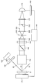
도 1은 본 발명의 일 실시예에 따른 기판의 결함 검출 장치를 나타낸 블럭도이다.1 is a block diagram showing an apparatus for detecting defects in a substrate according to an embodiment of the present invention.
도 1을 참조하면, 기판의 결함 검출 장치는 스테이지(110), 광원(120), 편광기(130), 필터(140), 대물 렌즈(150), 이미지 센서(160), 검출부(170) 및 분석부(180)를 포함할 수 있다.Referring to FIG. 1, a defect detection device for a substrate includes a
스테이지(110)는 기판(S)을 지지할 수 있다. 기판(S)은 스테이지(110)의 상부면에 배치될 수 있다. 본 실시예에서, 기판(S)은 웨이퍼를 포함할 수 있다. 다른 실시예로서, 기판(S)은 유리 기판을 포함할 수도 있다. 스테이지(110)는 좌우 및 상하 방향으로 이동될 수 있다. 따라서, 스테이지(110)의 상부면에 안치된 기판(S)도 좌우 및 상하 방향으로 이동될 수 있다.The
광원(120)은 기초 빔(F)을 발생시킬 수 있다. 광원(120)은 기판(S)의 표면과 실질적으로 평행한 방향을 따라 기초 빔(F)을 발생시킬 수 있다. 따라서, 광원(120)은 스테이지(110)와 실질적으로 직교하는 방향을 따라 배치될 수 있다. 기초 빔(F)은 제 1 주파수(w)를 가질 수 있다. 다른 실시예로서, 광원(120)은 적어도 2개의 주파수들을 갖는 기초 빔을 발생시킬 수도 있다. 또한, 광원(120)에서 발생된 기초 빔(F)은 스팟 빔을 포함할 수 있다.The
필터(140)는 스테이지(110)의 상부에 배치될 수 있다. 또한, 필터(140)는 광원(120)에서 발생된 기초 빔(F)이 입사되는 위치에 배치될 수 있다. The
본 실시예에서, 필터(140)는 다이크로익 미러(dichroic mirror)를 포함할 수 있다. 다이크로익 미러는 미러의 표면에 유전체를 코팅한 구조를 가질 수 있다. 이러한 다이크로익 미러는 특정 주파수 대역의 빔만을 통과시키고, 그 이외의 주파수 대역들의 빔들은 반사시키는 기능을 가질 수 있다. 본 실시예에서 사용된 다이크로익 필터는 제 1 주파수(w) 대역의 빔은 반사시키고, 제 1 주파수(w)의 2배인 제 2 주파수(2w) 대역의 빔은 통과시킬 수 있다. 즉, 다이크로익 필터는 제 1 주파수(w)를 갖는 기초 빔(F)을 통과시키지 않을 수 있다.In this embodiment, the
상기된 기능을 갖는 필터(140), 즉 다이크로익 미러는 기초 빔(F)의 진행 방향과 대략 45°경사지게 배치될 수 있다. 따라서, 필터(140)는 광원(120)에서 발생된 기초 빔(F)의 진행 방향을 기판(S)의 표면을 향해서 90°방향으로 전환시킬 수 있다. 따라서, 기초 빔(F)은 기판(S)의 표면과 실질적으로 직교하는 방향을 따라 기판(S)의 표면으로 입사될 수 있다.The
편광기(130)는 광원(120)과 필터(140) 사이에 배치될 수 있다. 편광기(130)는 광원(120)에서 발생된 기초 빔(F)을 편광시켜서, 특정한 방향성을 갖는 편광 빔(P)을 형성할 수 있다.The
편광 빔(P)은 필터(140)로 입사될 수 있다. 편광 빔(P)은 제 1 주파수를 갖고 있으므로, 필터(140), 즉 다이크로익 미러는 편광 빔(P)을 기판(S)의 표면을 향해서 90°방향으로 전환시킬 수 있다.The polarization beam P may be incident on the
대물 렌즈(150)는 필터(140)와 스테이지(110) 사이에 배치될 수 있다. 필터(140)에서 반사된 입사 빔(I)은 대물 렌즈(150)을 통과해서 기판(S)의 표면과 실질적으로 직교하는 방향을 따라 스테이지(110) 상에 배치된 기판(S)의 표면으로 입사될 수 있다.The
입사 빔(I)이 입사된 기판(S)의 표면으로부터 반사 빔(R)이 발생될 수 있다. 반사 빔(R)은 제 1 주파수(w), 제 2 주파수(2w), 제 3 주파수(3w) 등을 가질 수 있다. 제 1 주파수(w)를 갖는 반사 빔(R)은 기판(S)의 표면으로부터 발생된 것일 수 있다. 반면에, 제 1 주파수(w)보다 2배인 제 2 주파수(2w)를 갖는 반사 빔(R)은 기판(S)의 표면에 묻은 결함으로부터 반사된 것일 수 있다. 즉, 제 2 주파수(2w)를 갖는 반사 빔(R)은 제 2 고조파수(SHG) 빔일 수 있다.The reflected beam R may be generated from the surface of the substrate S on which the incident beam I is incident. The reflected beam R may have a first frequency w, a second frequency 2w, a third frequency 3w, and the like. The reflection beam R having the first frequency w may be generated from the surface of the substrate S. On the other hand, the reflection beam R having the second frequency 2w, which is twice the first frequency w, may be reflected from defects on the surface of the substrate S. That is, the reflected beam R having the second frequency 2w may be a second harmonic (SHG) beam.
전술한 바와 같이, 필터(140)는 반사 빔(R) 중에서 SHG 빔만 통과시킬 수 있다. 즉, 제 1 주파수(w)와 제 3 주파수(3w)를 갖는 반사 빔(R)은 필터(140)를 통과할 수 없고, 제 2 주파수(2w)를 갖는 반사 빔(R), 즉 SHG 빔만이 필터(140)를 통과할 수 있다. As described above, the
필터(140)를 통과하지 못한 반사 빔(R)은 필터(140)로부터 반사될 수 있다. 필터(140)로부터 반사된 반사 빔(R)은 반사 미러(165) 및 렌즈(162)를 경유해서 이미지 센서(160)로 입사될 수 있다.The reflected beam R that has not passed through the
이미지 센서(160)는 반사 빔(R)을 이용해서 기판(S)의 표면으로 입사되는 입사 빔(I)을 포커싱할 수 있다. 구체적으로, 이미지 센서(150)는 반사 빔(R)의 포커싱 위치를 파악할 수 있다. 반사 빔(R)은 입사 빔(I)의 파장과 실질적으로 동일한 주파수를 갖고 있으므로, 이미지 센서(160)가 파악한 반사 빔(R)의 포커싱 위치가 입사 빔(I)의 포커싱 위치와 대응될 것이다. 본 실시예에서, 이미지 센서(160)는 CMOS 이미지 센서를 포함할 수 있다. The
이미지 센서(160)가 파악한 반사 빔(R)의 포커싱 위치는 분석부(180)로 전송될 수 있다. 분석부(180)는 입력된 포커싱 위치에 따라 스테이지(110)를 좌측 방향, 우측 방향, 상부 방향 및/또는 하부 방향으로 이동하여, 입사 빔(I)의 포커스가 기판(S)의 표면에 위치하도록 할 수 있다.The focusing position of the reflected beam R identified by the
검출부(170)는 필터(140)를 통과한 SHG 빔을 검출할 수 있다. SHG 빔은 렌즈(172)를 통해서 검출부(170)로 입사될 수 있다. 검출부(170)가 SHG 빔을 검출하면, 검출된 신호는 분석부(180)로 전송될 수 있다. 검출부(170)는 면적 스텝(area step) 방식 또는 면적 스캔(area scan) 방식으로 SHG 빔을 검출할 수 있다. 검출부(170)는 광증폭관(Photo Multiplier Tube : PMT), 이미지 센서, CCD 카메라 등을 포함할 수 있다. CCD 카메라는 EM(Electron Multiplying) CCD 카메라를 포함할 수 있다. 부가적으로, 증폭부(185)가 검출된 신호를 증폭시킬 수도 있다.The
분석부(180)가 SHG 빔의 검출 신호를 분석하여, 기판(S)의 표면에 결함이 존재하는 것으로 확인될 수 있다. 2개 이상의 주파수들을 갖는 입사 빔(I)이 기판(S)의 표면으로 입사되어 2개 이상의 주파수들을 갖는 SHG 빔들이 검출된 경우, 분석부(180)는 기판(S)의 표면에 서로 다른 크기들 및/또는 물성들을 갖는 결함이 기판(S)의 표면에 존재함을 확인할 수 있다. 특히, 나노 크기 이하의 결함이 기판(S)의 표면에 존재하는 것을 확인할 수 있다. 또한, 분석부(180)는 SHG 빔을 분석하여, 결함의 위치, 크기 및 물성에 대한 정보를 획득할 수 있다. The
도 2는 도 1의 장치를 이용해서 기판의 결함을 검출하는 방법을 순차적으로 나타낸 흐름도이다.FIG. 2 is a flowchart sequentially showing a method of detecting defects in a substrate using the apparatus of FIG. 1.
도 1 및 도 2를 참조하면, 단계 ST300에서, 광원(120)이 기초 빔(F)을 발생시킬 수 있다. 기초 빔(F)은 기판(S)의 표면과 실질적으로 평행한 방향을 따라 진행될 수 있다. 기초 빔(F)은 제 1 주파수(w)를 가질 수 있다. 다른 실시예로서, 기초 빔(F)은 2개 이상의 주파수들을 가질 수도 있다.1 and 2, in step ST300, the
단계 ST310에서, 편광기(130)가 기초 빔(F)을 편광시켜서, 특정한 방향성을 갖는 편광 빔(P)을 형성할 수 있다. 편광 빔(P)은 필터(140)로 입사될 수 있다.In step ST310, the
단계 ST320에서, 필터(140)가 편광 빔(P1)을 기판(S)의 표면을 향해서 반사시켜서, 기판(S)의 표면으로 입사되는 입사 빔(I)을 형성할 수 있다. In step ST320, the
단계 ST330에서, 필터(160)로부터 반사된 입사 빔(I)은 대물 렌즈(150)을 통과해서 기판(S)의 표면과 실질적으로 직교하는 방향을 따라 스테이지(110) 상에 배치된 기판(S)의 표면으로 입사될 수 있다.In step ST330, the incident beam I reflected from the
단계 ST340에서, 기판(S)의 표면으로부터 반사 빔(R)이 발생될 수 있다. 반사 빔(R)은 필터(140)로 입사될 수 있다. 필터(140)가 반사 빔(R) 중에서 SHG 빔만을 통과시킬 수 있다. 즉, 제 1 주파수(w)와 제 3 주파수(3w)를 갖는 반사 빔(R)은 필터(140)를 통과할 수 없고, 제 2 주파수(2w)를 갖는 반사 빔(R), 즉 SHG 빔만이 필터(140)를 통과할 수 있다. In step ST340, a reflective beam R may be generated from the surface of the substrate S. The reflected beam R may be incident on the
단계 ST350에서, 필터(140)를 통과하지 못한 반사 빔(R)은 필터(140)로부터 반사될 수 있다. 필터(140)로부터 반사된 반사 빔(R)은 반사 미러(165) 및 렌즈(162)를 경유해서 이미지 센서(160)로 입사될 수 있다.In step ST350, the reflected beam R that has not passed through the
단계 ST360에서, 이미지 센서(160)가 반사 빔(R)을 이용해서 기판(S)의 표면으로 입사되는 입사 빔(I)을 포커싱할 수 있다. 이미지 센서(160)는 반사 빔(RI)의 포커싱 위치를 파악할 수 있다. 이미지 센서(160)에 의해 파악된 포커싱 위치는 분석부(180)로 전송될 수 있다.In step ST360, the
단계 ST370에서, 분석부(180)는 전송된 포커싱 위치에 따라 스테이지(110)를 좌측 방향, 우측 방향, 상부 방향 및/또는 하부 방향으로 이동시켜서, 입사 빔(I)의 포커스가 기판(S)의 표면에 위치하도록 할 수 있다.In step ST370, the
단계 ST380에서, 검출부(170)가 필터(140)를 통과한 SHG 빔을 검출할 수 있다. 검출부(170)가 SHG 빔을 검출하면, 검출된 신호는 분석부(180)로 전송될 수 있다. 검출부(170)는 면적 스텝(area step) 방식 또는 면적 스캔(area scan) 방식으로 SHG 빔을 검출할 수 있다. 부가적으로, 증폭부(185)가 검출된 신호를 증폭시킬 수도 있다. In step ST380, the
단계 ST390에서, 분석부(180)가 SHG 빔의 검출 신호를 분석하여, 기판(S)의 표면에 결함이 존재하는 것으로 확인될 수 있다. 2개 이상의 주파수들을 갖는 입사 빔(I)이 기판(S)의 표면으로 입사되어 2개 이상의 주파수들을 갖는 SHG 빔들이 검출된 경우, 분석부(180)는 기판(S)의 표면에 서로 다른 크기들 및/또는 물성들을 갖는 결함이 기판(S)의 표면에 존재함을 확인할 수 있다. 특히, 나노 크기 이하의 결함이 기판(S)의 표면에 존재하는 것을 확인할 수 있다. 또한, 분석부(180)는 SHG 빔을 분석하여, 결함의 위치, 크기 및 물성에 대한 정보를 획득할 수 있다. In step ST390, the
도 3은 본 발명의 다른 실시예에 따른 기판의 결함 검출 장치를 나타낸 블럭도이다.3 is a block diagram showing an apparatus for detecting defects in a substrate according to another embodiment of the present invention.
본 실시예에 따른 기판의 결함 검출 장치는 분석기 및 공간 필터를 더 포함한다는 점을 제외하고는 도 1에 도시된 장치의 구성요소들과 실질적으로 동일한 구성요소들을 포함할 수 있다. 따라서, 동일한 구성요소들을 동일한 참조부호들로 나타내고, 또한 동일한 구성요소들에 대한 반복 설명은 생략할 수 있다.The apparatus for detecting defects in a substrate according to the present embodiment may include substantially the same components as those of the apparatus shown in FIG. 1 except that it further includes an analyzer and a spatial filter. Therefore, the same components are denoted by the same reference numerals, and repeated descriptions of the same components can be omitted.
도 3을 참조하면, 전술한 바와 같이, 필터(140)는 결함에 기인한 제 2 주파수(2w)를 갖는 SHG 빔만을 통과시킬 수 있다. 그러나, 필터(140)를 통과한 SHG 빔 내에는 결함에 기인하지 않은 빔, 예를 들어서, 기판(S)의 표면으로부터 발생된 빔이 부분적으로 포함될 수도 있다. 이러한 빔은 SHG 빔의 방향과 다른 방향을 가질 수 있다.Referring to FIG. 3, as described above, the
분석기(analyzer)(190)는 필터(140)와 검출부(170) 사이에 배치될 수 있다. 분석기(190)는 필터(140)를 통과한 SHG 빔으로부터 SHG 빔의 방향과 다른 방향을 갖는 빔을 제거할 수 있다. 따라서, 분석기(190)를 통과한 SHG 빔은 동일한 방향을 가질 수 있다.The
공간 필터(spatial filter)(200)는 분석기(190)와 검출부(170) 사이에 배치될 수 있다. 분석기(190)를 통과한 SHG 빔은 렌즈(192)에 의해서 공간 필터(200)로 집중될 수 있다. 공간 필터(200)는 분석기(190)를 통과한 SHG 빔 내에 포함된 노이즈를 제거할 수 있다. 예를 들어서, 분석기(190)를 통과한 SHG 빔은 제 2 주파수 대역뿐만 아니라 제 2 주파수 대역보다 약간 낮거나 높은 주파수를 가질 수도 있다. 제 2 주파수 대역보다 약간 낮거나 높은 SHG 빔 부분은 검출부(170)에서 획득하게 되는 이미지의 화질을 저하시키는 노이즈로 작용할 수 있다. 공간 필터(200)는 제 2 주파수 대역보다 약간 낮거나 높은 SHG 빔 부분과 같은 노이즈를 SHG 빔으로부터 제거할 수 있다.The
공간 필터(200)를 통과한 SHG 빔은 렌즈(202)에 의해서 평행하게 유도될 수 있다. 평행하게 유도된 SHG 빔은 렌즈(172)를 통해서 검출부(170)로 입사될 수 있다.The SHG beam passing through the
도 4는 도 3의 장치를 이용해서 기판의 결함을 검출하는 방법을 순차적으로 나타낸 흐름도이다.4 is a flowchart sequentially showing a method of detecting defects in a substrate using the apparatus of FIG. 3.
도 3 및 도 4를 참조하면, 도 2를 참조로 설명된 단계 ST300 내지 단계 ST370을 순차적으로 수행할 수 있다.3 and 4, steps ST300 to ST370 described with reference to FIG. 2 may be sequentially performed.
단계 ST372에서, 분석기(190)가 필터(140)를 통과한 SHG 빔으로부터 SHG 빔의 방향과 다른 방향을 갖는 빔을 제거할 수 있다. 따라서, 분석기(190)를 통과한 SHG 빔은 동일한 방향을 가질 수 있다.In step ST372, the
단계 ST374에서, 공간 필터(200)가 분석기(190)를 통과한 SHG 빔 내에 포함된 노이즈를 제거할 수 있다. 예를 들어서, 분석기(190)를 통과한 SHG 빔은 제 2 주파수 대역뿐만 아니라 제 2 주파수 대역보다 약간 낮거나 높은 주파수를 가질 수도 있다. 제 2 주파수 대역보다 약간 낮거나 높은 SHG 빔 부분은 검출부(170)에서 획득하게 되는 이미지의 화질을 저하시키는 노이즈로 작용할 수 있다. 공간 필터(200)는 제 2 주파수 대역보다 약간 낮거나 높은 SHG 빔 부분과 같은 노이즈를 SHG 빔으로부터 제거하여, 검출부(170)에서 획득한 이미지의 화질을 향상시킬 수 있다.In step ST374, the
단계 ST382에서, 검출부(170)가 공간 필터(200)를 통과한 SHG 빔을 검출할 수 있다. 검출부(170)가 SHG 빔을 검출하면, 검출된 신호는 분석부(180)로 전송될 수 있다. 검출부(170)는 면적 스텝(area step) 방식 또는 면적 스캔(area scan) 방식으로 SHG 빔을 검출할 수 있다. 부가적으로, 증폭부(185)가 검출된 신호를 증폭시킬 수도 있다. In step ST382, the
단계 ST390에서, 분석부(180)가 SHG 빔의 검출 신호를 분석하여, 기판(S)의 표면에 결함이 존재하는 것으로 확인될 수 있다. 2개 이상의 주파수들을 갖는 입사 빔(I)이 기판(S)의 표면으로 입사되어 2개 이상의 주파수들을 갖는 SHG 빔들이 검출된 경우, 분석부(180)는 기판(S)의 표면에 서로 다른 크기들 및/또는 물성들을 갖는 결함이 기판(S)의 표면에 존재함을 확인할 수 있다. 특히, 나노 크기 이하의 결함이 기판(S)의 표면에 존재하는 것을 확인할 수 있다. 또한, 분석부(180)는 SHG 빔을 분석하여, 결함의 위치, 크기 및 물성에 대한 정보를 획득할 수 있다. In step ST390, the
도 5는 본 발명의 또 다른 실시예에 따른 기판의 결함 검출 장치를 나타낸 블럭도이다.5 is a block diagram showing an apparatus for detecting defects in a substrate according to another embodiment of the present invention.
본 실시예에 따른 기판의 결함 검출 장치는 차단판을 더 포함한다는 점을 제외하고는 도 3에 도시된 장치의 구성요소들과 실질적으로 동일한 구성요소들을 포함할 수 있다. 따라서, 동일한 구성요소들을 동일한 참조부호들로 나타내고, 또한 동일한 구성요소들에 대한 반복 설명은 생략할 수 있다.The apparatus for detecting defects in a substrate according to the present embodiment may include components substantially the same as those of the apparatus shown in FIG. 3, except that it further includes a blocking plate. Therefore, the same components are denoted by the same reference numerals, and repeated descriptions of the same components can be omitted.
도 5를 참조하면, 차단판(210)은 공간 필터(200)와 검출부(170) 사이에 배치될 수 있다. 차단판(210)은 공간 필터(200)로부터 검출부(170)로 입사되는 SHG 빔의 중앙 부위를 차단할 수 있다.Referring to FIG. 5, the blocking
공간 필터(200)를 통과한 SHG 빔의 중앙 부위에는 결함이 아닌 기판(S)의 표면으로부터 발생된 빔이 부분적으로 포함될 수 있다. 기판(S)의 표면으로부터 발생된 빔은 SHG 빔의 노이즈로 작용하게 되므로, 차단판(210)이 SHG 빔의 중앙 부위를 차단하여, 검출부(170)로 입사되지 않도록 할 수 있다.The central portion of the SHG beam passing through the
도 6은 도 5의 장치를 이용해서 기판의 결함을 검출하는 방법을 순차적으로 나타낸 흐름도이다.6 is a flowchart sequentially showing a method of detecting defects in a substrate using the apparatus of FIG. 5.
도 5 및 도 6을 참조하면, 도 4를 참조로 설명된 단계 ST300 내지 단계 ST374을 순차적으로 수행할 수 있다.5 and 6, steps ST300 to ST374 described with reference to FIG. 4 may be sequentially performed.
단계 ST376에서, 차단판(210)이 공간 필터(200)를 통과한 SHG 빔의 중앙 부위를 차단할 수 있다. 따라서, SHG 빔의 중앙 부위는 검출부(170)로 입사되지 않을 수 있다.In step ST376, the blocking
단계 ST384에서, 검출부(170)가 차단판(210)에 의해 차단되지 않은 SHG 빔을 검출할 수 있다. 검출부(170)가 SHG 빔을 검출하면, 검출된 신호는 분석부(180)로 전송될 수 있다. 검출부(170)는 면적 스텝(area step) 방식 또는 면적 스캔(area scan) 방식으로 SHG 빔을 검출할 수 있다. 부가적으로, 증폭부(185)가 검출된 신호를 증폭시킬 수도 있다. In step ST384, the
단계 ST390에서, 분석부(180)가 SHG 빔의 검출 신호를 분석하여, 기판(S)의 표면에 결함이 존재하는 것으로 확인될 수 있다. 2개 이상의 주파수들을 갖는 입사 빔(I)이 기판(S)의 표면으로 입사되어 2개 이상의 주파수들을 갖는 SHG 빔들이 검출된 경우, 분석부(180)는 기판(S)의 표면에 서로 다른 크기들 및/또는 물성들을 갖는 결함이 기판(S)의 표면에 존재함을 확인할 수 있다. 특히, 나노 크기 이하의 결함이 기판(S)의 표면에 존재하는 것을 확인할 수 있다. 또한, 분석부(180)는 SHG 빔을 분석하여, 결함의 위치, 크기 및 물성에 대한 정보를 획득할 수 있다. In step ST390, the
도 7은 본 발명의 또 다른 실시예에 따른 기판의 결함 검출 장치를 나타낸 블럭도이다.7 is a block diagram showing an apparatus for detecting defects in a substrate according to another embodiment of the present invention.
본 실시예에 따른 기판의 결함 검출 장치는 원통형 렌즈를 더 포함한다는 점을 제외하고는 도 5에 도시된 장치의 구성요소들과 실질적으로 동일한 구성요소들을 포함할 수 있다. 따라서, 동일한 구성요소들을 동일한 참조부호들로 나타내고, 또한 동일한 구성요소들에 대한 반복 설명은 생략할 수 있다.The apparatus for detecting defects in a substrate according to the present embodiment may include substantially the same components as those of the apparatus shown in FIG. 5, except that it further includes a cylindrical lens. Therefore, the same components are denoted by the same reference numerals, and repeated descriptions of the same components can be omitted.
도 7을 참조하면, 본 실시예의 검출 장치는 라인 빔을 사용할 수 있다. 이를 위해서, 원통형 렌즈(145)는 편광기(130)와 필터(140) 사이에 배치될 수 있다. 원통형 렌즈(145)는 편광기(130)에 의해 편광된 편광 빔(P)을 라인 빔(L)으로 변환시킬 수 있다. 따라서, 원통형 렌즈(145)에 의해 변한된 라인 빔(L)이 필터(140)로 입사될 수 있다.Referring to FIG. 7, the detection apparatus of this embodiment may use a line beam. To this end, the
본 실시예의 장치를 이용해서 기판 상의 결함을 검출하는 방법은 라인 빔을 이용한다는 점을 제외하고는 도 6을 참조로 설명한 방법과 실질적으로 동일할 수 있다. 따라서, 본 실시예의 장치를 이용해서 기판 상의 결함을 검출하는 방법에 대한 반복 설명은 생략할 수 있다.The method of detecting defects on the substrate using the apparatus of this embodiment may be substantially the same as the method described with reference to FIG. 6, except that a line beam is used. Therefore, repeated description of the method for detecting defects on the substrate using the apparatus of this embodiment can be omitted.
다른 실시예로서, 원통형 렌즈(145)는 도 1에 도시된 장치 또는 도 3에 도시된 장치에도 적용될 수 있다.As another embodiment, the
도 8은 본 발명의 또 다른 실시예에 따른 기판의 결함 검출 장치를 나타낸 블럭도이다.8 is a block diagram showing an apparatus for detecting defects in a substrate according to another embodiment of the present invention.
본 실시예에 따른 기판의 결함 검출 장치는 콜리메이팅 렌즈를 더 포함한다는 점을 제외하고는 도 5에 도시된 장치의 구성요소들과 실질적으로 동일한 구성요소들을 포함할 수 있다. 따라서, 동일한 구성요소들을 동일한 참조부호들로 나타내고, 또한 동일한 구성요소들에 대한 반복 설명은 생략할 수 있다.The apparatus for detecting defects in a substrate according to the present embodiment may include components substantially the same as those of the apparatus shown in FIG. 5, except that the collimating lens is further included. Therefore, the same components are denoted by the same reference numerals, and repeated descriptions of the same components can be omitted.
도 8을 참조하면, 본 실시예의 검출 장치는 평행 빔을 이용할 수 있다. 이를 위해서, 콜리메이팅 렌즈(125)가 광원(120)과 편광기(130) 사이에 배치될 수 있다. 광원(120)에서 발생된 기초 빔(F)은 콜레메이팅 렌즈(125)에 의해 평행 빔(C)으로 변환될 수 있다. 따라서, 평행 빔(C)이 편광기(130)로 입사될 수 있다.Referring to FIG. 8, the detection device of this embodiment may use a parallel beam. To this end, a
평행 빔(C)이 사용되므로, 필터(140)에 의해 반사된 입사 빔(I)은 대물 렌즈(150)를 거치지 않고 기판(S)으로 직접 입사될 수 있다. 따라서, 대물 렌즈(150)는 필터(150)와 분석기(190) 사이에 배치될 수 있다.Since the parallel beam C is used, the incident beam I reflected by the
다른 실시예로서, 콜레메이팅 렌즈(125)는 도 1에 도시된 장치 또는 도 3에 도시된 장치에도 적용될 수 있다.As another embodiment, the
도 9는 도 8의 장치를 이용해서 기판의 결함을 검출하는 방법을 순차적으로 나타낸 흐름도이다.9 is a flowchart sequentially showing a method of detecting a defect in a substrate using the apparatus of FIG. 8.
도 8 및 도 9를 참조하면, 단계 ST300에서, 광원(120)이 기초 빔(F)을 발생시킬 수 있다. 기초 빔(F)은 기판(S)의 표면과 실질적으로 평행한 방향을 따라 진행될 수 있다. 기초 빔(F)은 제 1 주파수(w)를 가질 수 있다. 8 and 9, in step ST300, the
단계 ST302에서, 콜레메이팅 렌즈(125)가 기초 빔(F)을 평행 빔(C)으로 변환시킬 수 있다.In step ST302, the
단계 ST312에서, 편광기(130)가 평행 빔(C)을 편광시켜서 편광 빔(P)을 형성할 수 있다.In step ST312, the
이어서, 도 6을 참조로 설명한 단계 ST320 내지 ST390을 순차적으로 수행하여, 기판(S) 상의 결함을 검출할 수 있다.Subsequently, steps ST320 to ST390 described with reference to FIG. 6 may be sequentially performed to detect defects on the substrate S.
도 10은 본 발명의 또 다른 실시예에 따른 기판의 결함 검출 장치를 나타낸 블럭도이다.10 is a block diagram showing an apparatus for detecting defects in a substrate according to another embodiment of the present invention.
도 10을 참조하면, 기판의 결함 검출 장치는 스테이지(110), 광원(122), 편광기(132), 필터(140), 대물 렌즈(150), 이미지 센서(160), 검출부(170), 분석부(180), 분석기(190), 공간 필터(200) 및 차단판(210)을 포함할 수 있다.Referring to FIG. 10, the defect detection device of the substrate includes a
스테이지(110), 필터(140), 대물 렌즈(150), 이미지 센서(160), 검출부(170), 분석부(180), 분석기(190), 공간 필터(200) 및 차단판(210)은 도 6에 도시된 스테이지(110), 필터(140), 대물 렌즈(150), 이미지 센서(160), 검출부(170), 분석부(180), 분석기(190), 공간 필터(200) 및 차단판(210) 각각과 실질적으로 동일한 구조 및 기능을 가지므로, 상기된 구성요소들에 대한 반복 설명은 생략할 수 있다.The
광원(122)은 기판(S)의 표면과 경사진 방향을 따라 기초 빔(F1)을 발생시킬 수 있다. 따라서, 광원(122)은 스테이지(110)와 경사진 방향을 따라 배치될 수 있다. The
편광기(132)는 광원(122)과 필터(140) 사이에 배치될 수 있다. 광원(122)이 스테이지(110)와 경사진 방향을 따라 배치되므로, 편광기(132)도 스테이지(110)와 경사진 방향을 따라 배치될 수 있다. 편광기(132)는 광원(122)에서 발생된 기초 빔(F1)을 편광시켜서, 특정한 방향성을 갖는 편광 빔(P1)을 형성할 수 있다.The
편광 빔(P1)이 스테이지(110) 상에 배치된 기판(S)의 표면으로 직접 입사될 수 있다. 기판(S)의 표면에서 발생된 반사 빔(R1)은 기판(S)의 표면과 경사진 방향을 따라 진행될 수 있다. 반면에, 기판(S)의 표면에 묻은 결함으로부터 발생된 반사 빔(R2)은 대물 렌즈(150)를 통해서 필터(140)로 입사될 수 있다. The polarization beam P1 may be directly incident on the surface of the substrate S disposed on the
도 11은 도 10의 장치를 이용해서 기판의 결함을 검출하는 방법을 순차적으로 나타낸 흐름도이다.11 is a flowchart sequentially showing a method of detecting a defect in a substrate using the apparatus of FIG. 10.
도 10 및 도 11을 참조하면, 단계 ST304에서, 광원(122)이 기판(S)의 표면과 경사진 방향을 따라 기초 빔(F1)을 발생시킬 수 있다.10 and 11, in step ST304, the
단계 ST314에서, 편광기(132)가 기초 빔(F1)을 편광시켜서, 편광 빔(P1)을 형성할 수 있다.In step ST314, the
단계 ST332에서, 편광 빔(P1)이 스테이지(110) 상에 안치된 기판(S)의 표면으로 경사지게 입사될 수 있다.In step ST332, the polarizing beam P1 may be inclined to the surface of the substrate S placed on the
이어서, 도 6을 참조로 설명한 단계 ST340 내지 단계 ST390을 순차적으로 수행하여, 기판(S) 표면의 결함을 정확하게 검출할 수 있다.Subsequently, steps ST340 to ST390 described with reference to FIG. 6 may be sequentially performed to accurately detect defects on the surface of the substrate S.
상기된 본 실시예들에 따르면, 기판의 표면으로부터 발생된 반사광 중에서 기판의 표면에 위치한 결함에 기인한 SHG 빔만을 검출할 수 있다. 따라서, 나노 크기 이하의 미세한 결함을 SHG 빔의 검출을 통해서 정확하면서 신속하게 검출할 수 있다.According to the above-described embodiments, only the SHG beam due to a defect located on the surface of the substrate can be detected among the reflected light generated from the surface of the substrate. Therefore, it is possible to accurately and quickly detect minute defects of nano size or less through detection of the SHG beam.
상술한 바와 같이, 본 발명의 바람직한 실시예들을 참조하여 설명하였지만 해당 기술 분야의 숙련된 당업자라면 하기의 특허 청구의 범위에 기재된 본 발명의 사상으로부터 벗어나지 않는 범위 내에서 본 발명을 다양하게 수정 및 변경시킬 수 있음을 이해할 수 있을 것이다.As described above, although described with reference to preferred embodiments of the present invention, those skilled in the art variously modify and change the present invention without departing from the spirit of the present invention as set forth in the claims below. You can understand that you can.
F ; 기초 빔
P ; 편광 빔
I ; 입사 빔
R ; 반사 빔
110 ; 스테이지
120 ; 광원
130 ; 편광기
140 ; 필터
150 ; 대물 렌즈
160 ; 이미지 센서
170 ; 검출부
180 ; 분석부
185 ; 증폭부
190 ; 분석기
200 ; 공간 필터
210 ; 차단판F; Foundation beam P; Polarized beam
I; Incident beam R; Reflective beam
110;
130;
150;
170;
185;
200;
Claims (20)
상기 입사 빔에 의해서 상기 기판의 표면으로부터 발생된 반사 빔 중에서 상기 기판의 표면에 위치한 결함에 기인한 제 2 고조파수(Second Harmonic Generation : SHG) 빔을 검출하는 것을 포함하는 기판의 결함 검출 방법.Irradiating the incident beam onto the surface of the substrate and
And detecting a second harmonic generation (SHG) beam due to a defect located on the surface of the substrate among the reflected beams generated from the surface of the substrate by the incident beam.
상기 입사 빔에 의해서 상기 기판의 표면으로부터 발생된 반사 빔 중에서 상기 기판의 표면에 위치한 결함에 기인한 제 2 고조파수(Second Harmonic Generation : SHG) 빔을 통과시키는 필터 및
상기 필터를 통과한 상기 SHG 빔을 검출하는 검출부를 포함하는 기판의 결함 검출 장치.A light source that generates an incident beam incident on the surface of the substrate
A filter for passing a second harmonic generation (SHG) beam due to a defect located on the surface of the substrate among the reflected beams generated from the surface of the substrate by the incident beam, and
A defect detection device for a substrate including a detection unit for detecting the SHG beam passing through the filter.
15. The apparatus of claim 13, further comprising an image sensor that focuses the incident beam on the surface of the substrate using the reflected beam.
Priority Applications (3)
| Application Number | Priority Date | Filing Date | Title |
|---|---|---|---|
| KR1020180111663A KR20200032801A (en) | 2018-09-18 | 2018-09-18 | Method of detecting a defect on a substrate and apparatus for performing the same |
| US16/364,251 US10816480B2 (en) | 2018-09-18 | 2019-03-26 | Method of detecting a defect on a substrate, apparatus for performing the same and method of manufacturing semiconductor device using the same |
| CN201910542195.5A CN110907471A (en) | 2018-09-18 | 2019-06-21 | Method of detecting defects on a substrate and apparatus for detecting defects on a substrate |
Applications Claiming Priority (1)
| Application Number | Priority Date | Filing Date | Title |
|---|---|---|---|
| KR1020180111663A KR20200032801A (en) | 2018-09-18 | 2018-09-18 | Method of detecting a defect on a substrate and apparatus for performing the same |
Publications (1)
| Publication Number | Publication Date |
|---|---|
| KR20200032801A true KR20200032801A (en) | 2020-03-27 |
Family
ID=69772138
Family Applications (1)
| Application Number | Title | Priority Date | Filing Date |
|---|---|---|---|
| KR1020180111663A KR20200032801A (en) | 2018-09-18 | 2018-09-18 | Method of detecting a defect on a substrate and apparatus for performing the same |
Country Status (3)
| Country | Link |
|---|---|
| US (1) | US10816480B2 (en) |
| KR (1) | KR20200032801A (en) |
| CN (1) | CN110907471A (en) |
Cited By (1)
| Publication number | Priority date | Publication date | Assignee | Title |
|---|---|---|---|---|
| WO2022241141A1 (en) * | 2021-05-12 | 2022-11-17 | Femtometrix, Inc. | Second-harmonic generation for critical dimensional metrology |
Families Citing this family (2)
| Publication number | Priority date | Publication date | Assignee | Title |
|---|---|---|---|---|
| JP7181051B2 (en) * | 2018-10-18 | 2022-11-30 | シャープ株式会社 | Document feeder and image forming device |
| CN112485272B (en) * | 2020-12-14 | 2021-11-09 | 紫创(南京)科技有限公司 | Semiconductor detection device and detection method |
Family Cites Families (13)
| Publication number | Priority date | Publication date | Assignee | Title |
|---|---|---|---|---|
| JPH0816607B2 (en) * | 1990-10-30 | 1996-02-21 | インターナショナル・ビジネス・マシーンズ・コーポレイション | Thin film processing control method |
| JPH07260702A (en) | 1994-03-24 | 1995-10-13 | Nec Corp | Inspection method of interface and equipment therefor |
| JPH07318500A (en) * | 1994-05-23 | 1995-12-08 | Hitachi Ltd | Inspection device for vicinity of object surface |
| US6791099B2 (en) | 2001-02-14 | 2004-09-14 | Applied Materials, Inc. | Laser scanning wafer inspection using nonlinear optical phenomena |
| JP3996774B2 (en) | 2002-01-09 | 2007-10-24 | 株式会社日立ハイテクノロジーズ | Pattern defect inspection method and pattern defect inspection apparatus |
| JP2010085225A (en) | 2008-09-30 | 2010-04-15 | Epson Toyocom Corp | Etching defect inspection method of piezoelectric vibrating chip wafer, and inspection system |
| CN102095690A (en) * | 2010-12-20 | 2011-06-15 | 福建师范大学 | Polarization imaging nondestructive detection device |
| EP3062146B1 (en) * | 2013-10-25 | 2020-01-22 | Nikon Corporation | Laser device, and exposure device and inspection device provided with laser device |
| CN104655592A (en) * | 2013-11-19 | 2015-05-27 | 有研光电新材料有限责任公司 | Apparatus and method for testing laser frequency doubling crystal properties |
| EP3132467A4 (en) * | 2014-04-17 | 2017-11-01 | Femtometrix, Inc. | Wafer metrology technologies |
| US9632020B2 (en) | 2014-10-22 | 2017-04-25 | The Boeing Company | Non-linear optical ellipsometry for surface monitoring and characterization |
| EP3218924B1 (en) | 2014-11-12 | 2020-02-12 | Femtometrix, Inc. | Systems for parsing material properties from within shg signals |
| US10928329B2 (en) * | 2017-10-11 | 2021-02-23 | Board Of Regents, The University Of Texas System | Method and system for optically detecting and characterizing defects in semiconductors |
-
2018
- 2018-09-18 KR KR1020180111663A patent/KR20200032801A/en not_active Application Discontinuation
-
2019
- 2019-03-26 US US16/364,251 patent/US10816480B2/en active Active
- 2019-06-21 CN CN201910542195.5A patent/CN110907471A/en active Pending
Cited By (1)
| Publication number | Priority date | Publication date | Assignee | Title |
|---|---|---|---|---|
| WO2022241141A1 (en) * | 2021-05-12 | 2022-11-17 | Femtometrix, Inc. | Second-harmonic generation for critical dimensional metrology |
Also Published As
| Publication number | Publication date |
|---|---|
| US20200088649A1 (en) | 2020-03-19 |
| US10816480B2 (en) | 2020-10-27 |
| CN110907471A (en) | 2020-03-24 |
Similar Documents
| Publication | Publication Date | Title |
|---|---|---|
| US9970883B2 (en) | Multi-spot scanning collection optics | |
| KR20200032801A (en) | Method of detecting a defect on a substrate and apparatus for performing the same | |
| KR102228505B1 (en) | Surface defect inspection using large particle monitoring and laser power control | |
| JP3978528B2 (en) | Pattern defect inspection apparatus and laser microscope | |
| US20070109546A1 (en) | Scanning Microscopy | |
| US9976903B2 (en) | Spectrometer and method of spectroscopy | |
| JP2012078164A (en) | Pattern inspection device | |
| WO2020007370A1 (en) | Detecting device and method | |
| JPWO2005124321A1 (en) | measuring device | |
| US20090079969A1 (en) | Method and apparatus for scatterfield microscopical measurement | |
| KR20210151709A (en) | Interferometric scattering microscopy | |
| JP2012026733A (en) | Optical defect detection device and method, and defect observation device provided with the same | |
| US20090161117A1 (en) | Inclined exposure lithography system | |
| TW202138750A (en) | Combined ocd and photoreflectance apparatus, system and method | |
| JP3282790B2 (en) | Defect inspection system for phase shift mask | |
| JP4961615B2 (en) | Photomask inspection method and apparatus | |
| KR20070091236A (en) | Defective particle measuring apparatus and defective particle measuring method | |
| JP2016015371A (en) | Thickness measurement apparatus, thickness measurement method and exposure apparatus | |
| JP4040777B2 (en) | Foreign matter inspection device | |
| JP2006258472A (en) | Defect inspection device | |
| JP2015224912A (en) | Defect measurement device and defect measurement method | |
| JPH07167793A (en) | Phase difference semiconductor inspection device and its production method | |
| JPH05142156A (en) | Foreign matter inspecting device | |
| JP2008224476A (en) | Photoluminescence measuring device | |
| JP2018054353A (en) | Near-field microscope |
Legal Events
| Date | Code | Title | Description |
|---|---|---|---|
| A201 | Request for examination | ||
| E902 | Notification of reason for refusal |