KR20190143604A - Bidirectional dc-dc converter - Google Patents
Bidirectional dc-dc converter Download PDFInfo
- Publication number
- KR20190143604A KR20190143604A KR1020180071231A KR20180071231A KR20190143604A KR 20190143604 A KR20190143604 A KR 20190143604A KR 1020180071231 A KR1020180071231 A KR 1020180071231A KR 20180071231 A KR20180071231 A KR 20180071231A KR 20190143604 A KR20190143604 A KR 20190143604A
- Authority
- KR
- South Korea
- Prior art keywords
- converter
- bidirectional
- mode
- leg
- inductor
- Prior art date
Links
Images


Classifications
-
- H—ELECTRICITY
- H02—GENERATION; CONVERSION OR DISTRIBUTION OF ELECTRIC POWER
- H02M—APPARATUS FOR CONVERSION BETWEEN AC AND AC, BETWEEN AC AND DC, OR BETWEEN DC AND DC, AND FOR USE WITH MAINS OR SIMILAR POWER SUPPLY SYSTEMS; CONVERSION OF DC OR AC INPUT POWER INTO SURGE OUTPUT POWER; CONTROL OR REGULATION THEREOF
- H02M3/00—Conversion of dc power input into dc power output
- H02M3/22—Conversion of dc power input into dc power output with intermediate conversion into ac
- H02M3/24—Conversion of dc power input into dc power output with intermediate conversion into ac by static converters
- H02M3/28—Conversion of dc power input into dc power output with intermediate conversion into ac by static converters using discharge tubes with control electrode or semiconductor devices with control electrode to produce the intermediate ac
- H02M3/325—Conversion of dc power input into dc power output with intermediate conversion into ac by static converters using discharge tubes with control electrode or semiconductor devices with control electrode to produce the intermediate ac using devices of a triode or a transistor type requiring continuous application of a control signal
- H02M3/335—Conversion of dc power input into dc power output with intermediate conversion into ac by static converters using discharge tubes with control electrode or semiconductor devices with control electrode to produce the intermediate ac using devices of a triode or a transistor type requiring continuous application of a control signal using semiconductor devices only
- H02M3/33569—Conversion of dc power input into dc power output with intermediate conversion into ac by static converters using discharge tubes with control electrode or semiconductor devices with control electrode to produce the intermediate ac using devices of a triode or a transistor type requiring continuous application of a control signal using semiconductor devices only having several active switching elements
- H02M3/33576—Conversion of dc power input into dc power output with intermediate conversion into ac by static converters using discharge tubes with control electrode or semiconductor devices with control electrode to produce the intermediate ac using devices of a triode or a transistor type requiring continuous application of a control signal using semiconductor devices only having several active switching elements having at least one active switching element at the secondary side of an isolation transformer
- H02M3/33584—Bidirectional converters
-
- H—ELECTRICITY
- H02—GENERATION; CONVERSION OR DISTRIBUTION OF ELECTRIC POWER
- H02M—APPARATUS FOR CONVERSION BETWEEN AC AND AC, BETWEEN AC AND DC, OR BETWEEN DC AND DC, AND FOR USE WITH MAINS OR SIMILAR POWER SUPPLY SYSTEMS; CONVERSION OF DC OR AC INPUT POWER INTO SURGE OUTPUT POWER; CONTROL OR REGULATION THEREOF
- H02M1/00—Details of apparatus for conversion
- H02M1/08—Circuits specially adapted for the generation of control voltages for semiconductor devices incorporated in static converters
- H02M1/083—Circuits specially adapted for the generation of control voltages for semiconductor devices incorporated in static converters for the ignition at the zero crossing of the voltage or the current
-
- H—ELECTRICITY
- H02—GENERATION; CONVERSION OR DISTRIBUTION OF ELECTRIC POWER
- H02M—APPARATUS FOR CONVERSION BETWEEN AC AND AC, BETWEEN AC AND DC, OR BETWEEN DC AND DC, AND FOR USE WITH MAINS OR SIMILAR POWER SUPPLY SYSTEMS; CONVERSION OF DC OR AC INPUT POWER INTO SURGE OUTPUT POWER; CONTROL OR REGULATION THEREOF
- H02M1/00—Details of apparatus for conversion
- H02M1/32—Means for protecting converters other than automatic disconnection
- H02M1/34—Snubber circuits
Abstract
Description
본 발명은 에너지 저장 시스템에 적용되는 양방향 직류-직류 컨버터(DC-DC convert)의 설계 기술에 관한 것으로, 특히 에너지 소스단과 배터리 셀 간에 에너지 교환 동작을 할 때, 에너지 밀도를 높이는 고주파 스위칭영역에서 발생하는 스위치와 인덕터의 손실을 줄일 수 있도록 한 양방향 직류-직류 컨버터에 관한 것이다.BACKGROUND OF THE
에너지 저장 시스템(ESS: Energy Stroge System)의 전체적인 구성은 전력 변환 장치인 PCS(Power Conversion System), 배터리 관리 시스템인 BMS(Battery Management System) 및 ESS를 제어하는 시스템인 EMS(Energy Management System)을 포함한다. PCS는 다양한 에너지원(Energy Source)으로부터 공급되는 전원을 상용의 교류전원(AC)으로 변환하거나 배터리 셀(Battery Cell)에 저장하는데 적당하도록 변환해 주는 장치이다. 여기서, DC 링크(Link) 단과 배터리 셀 간에 양방향으로 에너지 변환이 필요하게 되는데, 이 역할을 하는 전력 변환 장치를 양방향 직류-직류 컨버터라고 한다. The overall configuration of the Energy Stroge System (ESS) includes the Power Conversion System (PCS), a power conversion unit, the Battery Management System (BMS), and the Energy Management System (EMS), a system that controls the ESS. do. PCS is a device that converts power supplied from various energy sources into commercial AC power or suitable for storage in a battery cell. Here, the DC link stage and the battery cell Energy conversion is needed in both directions, and the power converter that plays this role is called a bidirectional DC-DC converter.
DC 링크단과 배터리 셀 간에 설치되는 양방향 직류-직류 컨버터의 효율을 향상시키면 양방향 직류-직류 컨버터에 사용되는 소자들의 크기를 줄일 수 있게 되므로 양방향 직류-직류 컨버터의 가격 경쟁력을 확보할 수 있다. 게다가, 소프트 스위칭을 통해 높은 효율 뿐아니라 EMI/EMC 노이즈 대책에도 유리하다. Improving the efficiency of the bidirectional DC-DC converter installed between the DC link stage and the battery cell can reduce the size of elements used in the bidirectional DC-DC converter, thereby securing the price competitiveness of the bidirectional DC-DC converter. In addition, soft switching is beneficial not only for high efficiency but also for EMI / EMC noise countermeasures.
일반적으로, 직류-직류 컨버터의 소자들을 좀 더 작은 소자로 사용하고자 하는 경우 직류-직류 컨버터의 스위칭 주파수를 높여주게 되는데, 이에 비례하여 스위치 손실이 크게 발생되는 문제점이 있다. 하지만, 직류-직류 컨버터의 스위칭 방식으로써, 소프트 스위칭의 일종인 ZVS(Zero Voltage Switching) 스위칭 방식을 채택하면 스위치 손실을 유발하지 않고 직류-직류 컨버터의 스위칭 주파수를 높일 수 있다. In general, when using elements of the DC-DC converter as a smaller device to increase the switching frequency of the DC-DC converter, there is a problem that a large switch loss occurs in proportion to this. However, when switching the DC-DC converter, the Zero Voltage Switching (ZVS) switching method, which is a kind of soft switching, can increase the switching frequency of the DC-DC converter without causing a switch loss.
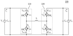
도 1은 종래 기술에 의한 양방향 직류-직류 컨버터의 회로도로서 이에 도시한 바와 같이 양방향 직류-직류 컨버터(100)는, 에너지원(Energy Source)으로부터 공급되는 전원인 디씨링크단전원(VL)에 병렬로 연결된 제1레그(110), 배터리 셀 모듈의 전원인 배터리전원(VH)에 병렬로 연결된 제2레그(120), 상기 제1레그(110)의 제1중간노드(N1)와 상기 제2레그(120)의 제2중간노드(N2)의 사이에 연결된 인덕터(L)를 포함한다. 여기서, 상기 제1레그(110)는 직렬 연결된 스위치(SW1,SW2)이고, 상기 제2레그(120)는 직렬 연결된 스위치(SW3,SW4)이다.1 is bi-directional direct current according to the prior art bi-directional direct current as shown in this illustrated a circuit diagram of a DC converter to
도 1을 참조하면, 제1레그(110)의 스위치(SW1,SW2)와 제2레그(120)의 스위치(SW3,SW4)가 상보적으로 스위칭 동작하여, 충전모드(Buck Mode)에서 디씨링크단전원(VL)이 인덕터(L)를 통해 배터리전원(VH)에 공급되거나, 방전모드(Boost Mode)에서 배터리전원(VH)이 인덕터(L)를 통해 디씨링크단전원(VL)에 공급된다. Referring to FIG. 1, the switches SW1 and SW2 of the
그런데, 이와 같은 종래 기술에 의한 양방향 직류-직류 컨버터는 고주파 동작에서 턴오프 손실(Turn off loss)과 코어 손실(Core loss)이 커서 효율이 저하되는 문제점이 있다. 이에 따라, 스위칭 주파수를 증가시켜 소자들의 사이즈를 줄이는데 어려움이 있고, 방열에 대한 대책이 추가적으로 요구되는 문제점이 있다. However, such a bidirectional DC-DC converter according to the related art has a problem in that efficiency is lowered due to large turn off loss and core loss in high frequency operation. Accordingly, it is difficult to reduce the size of the device by increasing the switching frequency, there is a problem that additional measures for heat dissipation are required.
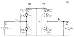
도 2는 종래 기술에 의한 또 다른 양방향 직류-직류 컨버터의 회로도로서 이에 도시한 바와 같이 양방향 직류-직류 컨버터(200)는, 직렬 연결된 스위치(SW1, SW2),(SW3,SW4)로 각기 이루어져 병렬 연결된 제1레그(210) 및 제2레그(220), 디씨링크단전원(VL)의 정극성 단자와 상기 제1레그(110)의 제1중간노드(N1)의 사이에 연결된 제1인덕터(L1) 및 배터리전원(VH)의 정극성 단자와 상기 제2레그(210)의 제2중간노드(N2)의 사이에 연결된 제2인덕터(L2)를 포함한다. FIG. 2 is a circuit diagram of another bidirectional DC-DC converter according to the prior art, and the bidirectional DC-
도 2를 참조하면, 제1레그(210)의 스위치(SW1,SW2)와 제2레그(220)의 스위치(SW3, SW4)가 상보적으로 스위칭 동작하여, 충전모드(Buck Mode)에서 디씨링크단전원(VL)이 제1인덕터(L1)를 통해 배터리전원(VH)에 공급되거나, 방전모드(Boost Mode)에서 배터리전원(VH)이 제2인덕터(L2)를 통해 디씨링크단전원(VL)에 공급된다. 이때, 제1,2레그(210),(220)에 병렬로 연결된 커패시터(Clink)와 제1,2인덕터(L1),(L2)로 인하여 입출력단의 필터 용량이 줄어들고, 양방향 직류-직류 컨버터(200)의 구조와 제어과정이 간단해 진다.Referring to FIG. 2, the switches SW1 and SW2 of the
그런데, 이와 같은 또 다른 종래 기술에 의한 양방향 직류-직류 컨버터는 디씨링크단전원이나 배터리전원의 전달 과정에서 추가적으로 소자를 사용하게 되므로, 양방향 직류-직류 컨버터 비용과 사이즈가 증가되는 문제점이 있고, 코어 손실량이 기본적인 구조를 갖는 양방향 직류-직류 컨버터에 비하여 증가되는 문제점이 있다.However, the bidirectional DC-DC converter according to another prior art as described above uses an additional element in the process of transferring DC link stage power or battery power, thereby increasing the cost and size of the bidirectional DC-DC converter. There is a problem that the amount of loss is increased compared to the bidirectional DC-DC converter having a basic structure.
본 발명이 해결하고자 하는 과제는 양방향 직류-직류 컨버터에서, 자기결합인덕터를 이용하여 코어의 자속(magnetic flux)을 저감시키고 누설 인덕터의 전류와 스너버 커패시터(Snubber Capacitor)를 이용하여 스위치에 대한 소프트 스위칭을 구현하여, 높은 스위칭 주파수를 사용할 수 있도록 하는데 있다.The problem to be solved by the present invention is to reduce the magnetic flux of the core by using a magnetic coupling inductor in the bidirectional DC-DC converter, and to use the current of the leakage inductor and the Snubber Capacitor to soften the switch. By implementing switching, it is possible to use a high switching frequency.
상기 기술적 과제를 이루기 위한 본 발명의 실시예에 따른 양방향 직류-직류 컨버터는, 직렬 연결된 제1,2스위치를 구비하여 디씨링크단전원인 입력전원에 병렬로 연결된 제1레그; 직렬 연결된 제3,4스위치를 구비하여 배터리 셀 모듈의 전원인 출력전원에 병렬로 연결된 제2레그; 상기 제1레그의 중간노드와 상기 입력전원의 부극성 단자의 사이에 연결된 제1스너버 커패시터; 상기 제2레그의 중간노드와 상기 입력전원의 부극성 단자의 사이에 연결된 제2스너버 커패시터; 및 상기 제1레그의 중간노드와 상기 제2레그의 중간노드의 사이에 연결된 자기결합 인덕터를 포함하는 것을 특징으로 한다.According to an aspect of the present invention, there is provided a bidirectional DC-DC converter, including: a first leg having first and second switches connected in series and connected in parallel to an input power source of a DC link stage power source; A second leg having third and fourth switches connected in series and connected in parallel to an output power source of a battery cell module; A first snubber capacitor connected between the intermediate node of the first leg and the negative terminal of the input power source; A second snubber capacitor connected between the intermediate node of the second leg and the negative terminal of the input power source; And a magnetic coupling inductor connected between the intermediate node of the first leg and the intermediate node of the second leg.
본 발명은 양방향 직류-직류 컨버터에서, 자기결합인덕터를 이용하여 코어의 자속(magnetic flux)을 저감시키고 누설 인덕터의 전류와 스너버 커패시터(Snubber Capacitor)를 이용하여 스위치에 대한 소프트 스위칭을 구현 함으로써, 높은 스위칭 주파수를 사용할 수 있는 효과가 있다.In the bidirectional DC-DC converter, the magnetic flux of the core is reduced by using a magnetic coupling inductor, and the soft switching of the switch is realized by using a leakage inductor and a snubber capacitor. There is an effect that high switching frequency can be used.
이에 따라, 양방향 직류-직류 컨버터 비용과 사이즈가 줄어들고, 코어 손실량이 기본적인 구조를 갖는 양방향 직류-직류 컨버터에 비하여 저감되는 효과가 있다.Accordingly, the cost and size of the bidirectional DC-DC converter are reduced, and the core loss amount is reduced as compared with the bidirectional DC-DC converter having a basic structure.
도 1은 종래 기술에 의한 양방향 직류-직류 컨버터의 회로도.
도 2는 종래 기술에 의한 또 다른 양방향 직류-직류 컨버터의 회로도.
도 3은 본 발명에 의한 양방향 직류-직류 컨버터의 회로도.
도 4는 양방향 직류-직류 컨버터가 부스트 컨버터 모드로 동작할 때 각부의 파형도.
도 5는 양방향 직류-직류 컨버터가 부스트 컨버터 모드로 동작할 때 각 모드별 소자들의 동작 상태를 나타낸 회로도.
도 6은 양방향 직류-직류 컨버터가 벅 컨버터 모드로 동작할 때 각부의 파형도.
도 7은 양방향 직류-직류 컨버터가 벅 컨버터 모드로 동작할 때 각 모드별 소자들의 동작 상태를 나타낸 회로도.1 is a circuit diagram of a bidirectional DC-DC converter according to the prior art.
2 is a circuit diagram of another bidirectional DC-DC converter according to the prior art.
3 is a circuit diagram of a bidirectional DC-DC converter according to the present invention.
4 is a waveform diagram of each part when the bidirectional DC-DC converter operates in the boost converter mode.
FIG. 5 is a circuit diagram illustrating an operation state of elements in each mode when the bidirectional DC-DC converter operates in the boost converter mode. FIG.
6 is a waveform diagram of each part when the bidirectional DC-DC converter operates in the buck converter mode.
FIG. 7 is a circuit diagram illustrating an operation state of elements in each mode when the bidirectional DC-DC converter operates in a buck converter mode. FIG.
이하, 첨부한 도면을 참조하여 본 발명의 바람직한 실시예를 상세히 설명하면 다음과 같다.Hereinafter, exemplary embodiments of the present invention will be described in detail with reference to the accompanying drawings.
도 3은 본 발명에 의한 양방향 직류-직류 컨버터의 회로도로서 이에 도시한 바와 같이 양방향 직류-직류 컨버터(300)는, 직렬 연결된 스위치(SW1,SW2)를 구비하여 에너지원(Energy Source)으로부터 공급되는 디씨링크단전원인 입력전원(VL)에 병렬로 연결된 제1레그(310); 직렬 연결된 스위치(SW3,SW4)를 구비하여 배터리 셀 모듈의 전원인 출력전원(![]()
![]()
![]()
![]()
![]()
![]()
![]()
![]()
![]()
![]()
![]()
![]()
![]()
![]()
![]()
![]()
![]()
![]()
![]()
![]()
![]()
![]()
양방향 직류-직류 컨버터(300)는 부스트 컨버터 모드(Boost Converter Mode)에서 출력전원(![]()
![]()
![]()
![]()
![]()
![]()
![]()
![]()
자기결합 인덕터(![]()
![]()
![]()
![]()
자기결합 인덕터(![]()
![]()
![]()
![]()
![]()
![]()
![]()
![]()
제1스너버 커패시터(![]()
![]()
![]()
![]()
제1레그(310)를 이루는 스위치(SW1,SW2)와 제2레그(320)를 이루는 스위치(SW3,SW4)는 입력전원(![]()
![]()
![]()
![]()
도 4는 양방향 직류-직류 컨버터(300)가 부스트 컨버터 모드로 동작할 때 각부의 파형도를 나타낸 것이고, 도 5는 양방향 직류-직류 컨버터(300)가 부스트 컨버터 모드로 동작할 때 각 모드별 소자들의 동작 상태를 나타낸 회로도이다. 도 4 및 도 5를 참조하여 양방향 직류-직류 컨버터(300)의 부스트 컨버터 모드의 동작을 설명하면 다음과 같다. 4 is a waveform diagram of each unit when the bidirectional DC-
도 5에서와 같이 부스트 컨버터 모드에서 스위치(SW1)는 항상 온 상태를 유지하고, 스위치(SW2)는 항상 오프 상태를 유지한다. 제1스너버 커패시터(![]()
![]()
![]()
![]()
제1모드(Mode 1)의 동작을 설명하면 다음과 같다. 제1모드(Mode 1)는 스위치(SW4)가 턴온되는 것에 의해 시작된다. 바로 이전의 제4모드(Mode 4)에서 스위치(SW4)의 바디 다이오드를 통해 전류가 흐르고 있었으므로 제1모드(Mode 1)에서도 계속해서 그 바디 다이오드를 통해 전류가 흐르게 된다. 1:1로 자기 결합된 자기결합 인덕터(Lm)에 포함되는 두 개의 누설 인덕터(![]()
![]()
![]()
![]()
![]()
![]()
![]()
![]()
![]()
![]()
![]()
![]()
제2모드(Mode 2)의 동작을 설명하면 다음과 같다. 제2모드(Mode 2)에서 스위치(SW4)가 턴오프된다. 이때, 스위치(SW4)가 턴오프 전류 중에서 대부분의 전류가 제2스너버 커패시터(![]()
![]()
![]()
![]()
![]()
![]()
![]()
![]()
제3모드(Mode 3)의 동작을 설명하면 다음과 같다. 제3모드(Mode 3)는 스위치(SW3)가 턴온되는 것에 의해 시작된다. 바로 이전의 제2모드(Mode 2)에서 스위치(SW3)의 바디 다이오드를 통해 전류가 흐르고 있었으므로 제3모드(Mode 3)에서도 계속해서 그 바디 다이오드를 통해 전류가 흐르게 된다. 상기 두 개의 누설 인덕터(![]()
![]()
![]()
![]()
![]()
![]()
![]()
![]()
![]()
![]()
제4모드(Mode 4)의 동작을 설명하면 다음과 같다. 제4모드(Mode 4)는 스위치(SW3)가 턴오프되는 것에 의해 시작된다. 이때 제2스너버 커패시터(![]()
![]()
![]()
![]()
![]()
![]()
도 6은 양방향 직류-직류 컨버터(300)가 벅 컨버터 모드로 동작할 때 각부의 파형도를 나타낸 것이고, 도 7은 양방향 직류-직류 컨버터(300)가 벅 컨버터 모드로 동작할 때 각 모드별 소자들의 동작 상태를 나타낸 회로도이다. 도 6 및 도 7을 참조하여 양방향 직류-직류 컨버터(300)의 벅 컨버터 모드의 동작을 설명하면 다음과 같다. FIG. 6 is a waveform diagram of each unit when the bidirectional DC-
도 7에서와 같이 벅 컨버터 모드에서 스위치(SW3)는 항상 온 상태를 유지하고, 스위치(SW4)는 항상 오프 상태를 유지한다. 제2스너버 커패시터(![]()
![]()
![]()
![]()
제1모드(Mode 1)의 동작을 설명하면 다음과 같다. 제1모드(Mode 1)는 스위치(SW1)가 턴온되는 것에 의해 시작된다. 바로 이전의 제4모드(Mode 4)에서 스위치(SW1)의 바디 다이오드를 통해 전류가 흐르고 있었으므로 제1모드(Mode 1)에서도 계속해서 그 바디 다이오드를 통해 전류가 흐르게 된다. 자기결합 인덕터(Lm)에 포함되는 두 개의 누설 인덕터(![]()
![]()
![]()
![]()
![]()
![]()
![]()
![]()
![]()
![]()
![]()
![]()
제2모드(Mode 2)의 동작을 설명하면 다음과 같다. 제2모드(Mode 2)에서 스위치(SW2)가 턴오프된다. 이때, 스위치(SW2)가 턴오프 전류 중에서 대부분의 전류가 제1스너버 커패시터(![]()
![]()
![]()
![]()
![]()
![]()
![]()
![]()
![]()
![]()
![]()
![]()
![]()
![]()
![]()
![]()
제3모드(Mode 3)의 동작을 설명하면 다음과 같다. 제3모드(Mode 3)는 스위치(SW2)가 턴온되는 것에 의해 시작된다. 바로 이전의 제2모드(Mode 2)에서 스위치(SW2)의 바디 다이오드를 통해 전류가 흐르고 있었으므로 제3모드(Mode 3)에서도 계속해서 그 바디 다이오드를 통해 전류가 흐르게 된다. 상기 두 개의 누설 인덕터(![]()
![]()
![]()
![]()
![]()
![]()
![]()
![]()
![]()
![]()
![]()
![]()
![]()
![]()
![]()
![]()
![]()
![]()
제4모드(Mode 4)의 동작을 설명하면 다음과 같다. 제4모드(Mode 4)는 스위치(SW2)가 턴오프되는 것에 의해 시작된다. 이때, 턴오프 전류의 대부분이 제1스너버 커패시터(![]()
![]()
![]()
![]()
![]()
![]()
![]()
![]()
![]()
![]()
![]()
![]()
![]()
![]()
![]()
![]()
![]()
![]()
양방향 직류-직류 컨버터(300)에서의 전압 변환 비율은 인덕터의 전압 발란싱(Voltage Second balance)에 의해 결정되는데, 부스트 컨버터 모드에서의 전압 변환 비율은 다음의 [수학식 1]로 표현된다.The voltage conversion ratio in the bidirectional DC-

여기서,"![]()
![]()
![]()
![]()
그리고, 양방향 직류-직류 컨버터(300)에서 벅 컨버터 모드의 전압 변환 비율은 다음의 [수학식 2]로 표현된다.In addition, the voltage conversion ratio of the buck converter mode in the bidirectional DC-

1:1로 자기 결합된 자기결합 인덕터(![]()
![]()

여기서, ![]()
![]()
![]()
![]()
![]()
![]()
![]()
![]()
![]()
![]()
![]()
![]()
상기 [수학식 3]을 정리하면 ![]()
![]()
![]()
![]()
상기 관계식들을 모두 연립하여 풀면 ![]()
![]()
![]()
![]()
따라서, 자기결합 인덕터(![]()
![]()
![]()
![]()
이상에서 본 발명의 바람직한 실시예에 대하여 상세히 설명하였지만, 본 발명의 권리범위가 이에 한정되는 것이 아니라 다음의 청구범위에서 정의하는 본 발명의 기본 개념을 바탕으로 보다 다양한 실시예로 구현될 수 있으며, 이러한 실시예들 또한 본 발명의 권리범위에 속하는 것이다. Although the preferred embodiment of the present invention has been described in detail above, the scope of the present invention is not limited thereto, and may be implemented in various embodiments based on the basic concept of the present invention defined in the following claims. Such embodiments are also within the scope of the present invention.
300 : 양방향 직류-직류 컨버터
310 : 제1레그
320 : 제2레그300: bidirectional DC-DC converter 310: first leg
320: second leg
Claims (7)
직렬 연결된 제3,4스위치를 구비하여 배터리 셀 모듈의 전원인 출력전원에 병렬로 연결된 제2레그;
상기 제1레그의 중간노드와 상기 입력전원의 부극성 단자의 사이에 연결된 제1스너버 커패시터;
상기 제2레그의 중간노드와 상기 입력전원의 부극성 단자의 사이에 연결된 제2스너버 커패시터; 및
상기 제1레그의 중간노드와 상기 제2레그의 중간노드의 사이에 연결된 자기결합 인덕터를 포함하는 것을 특징으로 하는 양방향 직류-직류 컨버터.
A first leg having first and second switches connected in series and connected in parallel to an input power source which is a DC link end power source;
A second leg having third and fourth switches connected in series and connected in parallel to an output power source of a battery cell module;
A first snubber capacitor connected between the intermediate node of the first leg and the negative terminal of the input power source;
A second snubber capacitor connected between the intermediate node of the second leg and the negative terminal of the input power source; And
And a magnetic coupling inductor coupled between the intermediate node of the first leg and the intermediate node of the second leg.
The bidirectional DC-DC converter of claim 1, wherein a turn-off current of the second switch flows through the first snubber capacitor.
상기 제1 내지 4 스위치의 ZVS(Zero Voltage Switching)를 위한 누설 인덕터를 포함하는 것을 특징으로 하는 양방향 직류-직류 컨버터.
The method of claim 1, wherein the magnetic coupling inductor
Bidirectional DC-DC converter comprising a leakage inductor for zero voltage switching (ZVS) of the first to fourth switches.
상기 자기결합 인덕터의 권선 수와 1,2차 권선 사이의 갭(gab)에 비례하여 높아지는 것을 특징으로 하는 양방향 직류-직류 컨버터.
The method of claim 4, wherein the inductance of the leakage inductor
The bidirectional DC-DC converter, characterized in that it increases in proportion to the gap (gab) between the number of turns of the magnetic coupling inductor and the primary and secondary windings.
상기 누설 인덕터의 인덕턴스에 의해 결정되는 것을 특징으로 하는 양방향 직류-직류 컨버터.
The method of claim 4, wherein the amount of current flowing through the first to fourth switches is
Bidirectional DC-DC converter, characterized in that determined by the inductance of the leakage inductor.
시리즈 에이딩 컨피규레이션(Series aiding configuration)에 의해 0 V가 되는 것을 특징으로 하는 양방향 직류-직류 컨버터.
The method of claim 1, wherein the voltage applied across the magnetic coupling inductor is
A bidirectional DC-DC converter characterized by being 0 V by Series aiding configuration.
Priority Applications (1)
| Application Number | Priority Date | Filing Date | Title |
|---|---|---|---|
| KR1020180071231A KR102076577B1 (en) | 2018-06-21 | 2018-06-21 | Bidirectional dc-dc converter |
Applications Claiming Priority (1)
| Application Number | Priority Date | Filing Date | Title |
|---|---|---|---|
| KR1020180071231A KR102076577B1 (en) | 2018-06-21 | 2018-06-21 | Bidirectional dc-dc converter |
Publications (2)
| Publication Number | Publication Date |
|---|---|
| KR20190143604A true KR20190143604A (en) | 2019-12-31 |
| KR102076577B1 KR102076577B1 (en) | 2020-02-13 |
Family
ID=69051827
Family Applications (1)
| Application Number | Title | Priority Date | Filing Date |
|---|---|---|---|
| KR1020180071231A KR102076577B1 (en) | 2018-06-21 | 2018-06-21 | Bidirectional dc-dc converter |
Country Status (1)
| Country | Link |
|---|---|
| KR (1) | KR102076577B1 (en) |
Citations (2)
| Publication number | Priority date | Publication date | Assignee | Title |
|---|---|---|---|---|
| US20160190932A1 (en) * | 2013-09-11 | 2016-06-30 | Fraunhofer-Gesellschaft Zur Foerderung Der Angewandten Forschung E.V. | Dc-dc converter |
| US20180041125A1 (en) * | 2016-08-03 | 2018-02-08 | Vlt, Inc. | Reducing switching losses in power converters |
-
2018
- 2018-06-21 KR KR1020180071231A patent/KR102076577B1/en active IP Right Grant
Patent Citations (2)
| Publication number | Priority date | Publication date | Assignee | Title |
|---|---|---|---|---|
| US20160190932A1 (en) * | 2013-09-11 | 2016-06-30 | Fraunhofer-Gesellschaft Zur Foerderung Der Angewandten Forschung E.V. | Dc-dc converter |
| US20180041125A1 (en) * | 2016-08-03 | 2018-02-08 | Vlt, Inc. | Reducing switching losses in power converters |
Non-Patent Citations (1)
| Title |
|---|
| 채준영 외, "결합 인덕터를 이용한 2상 양방향 비반전 벅-부스트 컨버터". 전력전자학회 논문지. 2014. * |
Also Published As
| Publication number | Publication date |
|---|---|
| KR102076577B1 (en) | 2020-02-13 |
Similar Documents
| Publication | Publication Date | Title |
|---|---|---|
| Wang et al. | A single switch quadratic boost high step up DC–DC converter | |
| US10833594B2 (en) | System and method of controlling a power converter having an LC tank coupled between a switching network and a transformer winding | |
| Kwon et al. | High gain soft-switching bidirectional DC–DC converter for eco-friendly vehicles | |
| US8743565B2 (en) | High power converter architecture | |
| US7746670B2 (en) | Dual-transformer type of DC-to-DC converter | |
| US7557546B2 (en) | Unidirectional DC-DC converter | |
| US9019724B2 (en) | High power converter architecture | |
| Kim et al. | Integrated dual full-bridge converter with current-doubler rectifier for EV charger | |
| JP2015159711A (en) | Switching power supply and power converter | |
| WO2014155604A1 (en) | Dc-dc converter | |
| US20090296429A1 (en) | Power converter load line control | |
| Hu et al. | A nonisolated bidirectional DC–DC converter with high voltage conversion ratio based on coupled inductor and switched capacitor | |
| CN103201939A (en) | Virtual parametric high side mosfet driver | |
| KR20180004675A (en) | Bidirectional Converter with Auxiliary LC Resonant Circuit and Operating Method thereof | |
| CN113746341A (en) | Switching converter, operating method thereof and controller circuit | |
| CN103647448B (en) | Integrated step-down-flyback type high power factor constant current circuit and device | |
| KR102488223B1 (en) | Charging system for electric vehicle with resonant dc-dc converter | |
| TW201541838A (en) | Flyback active clamping power converter | |
| CN110086354A (en) | Single-phase double push-pull booster circuit and step-up method based on silicon carbide MOSFET | |
| CN210807100U (en) | Power transmission circuit | |
| US20030147264A1 (en) | Circuit configuration combining synchronous rectifier circuit for converter with LC snubber circuit | |
| CN107222109B (en) | A kind of two-way isolated DC-DC converter containing active snubber | |
| IT201900007386A1 (en) | DC-DC converter | |
| US6400582B1 (en) | Dual forward power converter utilizing coupling capacitors for improved efficiency | |
| Wu et al. | Analysis and design for a new ZVS dc–dc converter with active clamping |
Legal Events
| Date | Code | Title | Description |
|---|---|---|---|
| A201 | Request for examination | ||
| E902 | Notification of reason for refusal | ||
| N231 | Notification of change of applicant | ||
| E701 | Decision to grant or registration of patent right |