KR20190104276A - Display device using micro led and manufacturing method thereof - Google Patents
Display device using micro led and manufacturing method thereof Download PDFInfo
- Publication number
- KR20190104276A KR20190104276A KR1020190101594A KR20190101594A KR20190104276A KR 20190104276 A KR20190104276 A KR 20190104276A KR 1020190101594 A KR1020190101594 A KR 1020190101594A KR 20190101594 A KR20190101594 A KR 20190101594A KR 20190104276 A KR20190104276 A KR 20190104276A
- Authority
- KR
- South Korea
- Prior art keywords
- light emitting
- semiconductor light
- emitting device
- assembly
- substrate
- Prior art date
Links
- 238000004519 manufacturing process Methods 0.000 title claims description 19
- 239000004065 semiconductor Substances 0.000 claims abstract description 403
- 239000000758 substrate Substances 0.000 claims abstract description 158
- 239000010410 layer Substances 0.000 claims description 92
- 238000000034 method Methods 0.000 claims description 63
- 238000005192 partition Methods 0.000 claims description 51
- 239000012790 adhesive layer Substances 0.000 claims description 41
- 238000012546 transfer Methods 0.000 claims description 15
- 230000033001 locomotion Effects 0.000 claims description 14
- 239000012530 fluid Substances 0.000 claims description 11
- 230000005684 electric field Effects 0.000 claims description 10
- 239000000696 magnetic material Substances 0.000 claims description 5
- 230000004888 barrier function Effects 0.000 claims description 4
- 239000003086 colorant Substances 0.000 abstract description 12
- 238000013461 design Methods 0.000 abstract description 2
- 230000008569 process Effects 0.000 description 32
- OAICVXFJPJFONN-UHFFFAOYSA-N Phosphorus Chemical compound [P] OAICVXFJPJFONN-UHFFFAOYSA-N 0.000 description 28
- 238000001338 self-assembly Methods 0.000 description 19
- 239000000463 material Substances 0.000 description 17
- 238000010586 diagram Methods 0.000 description 14
- 239000004642 Polyimide Substances 0.000 description 11
- 229920001721 polyimide Polymers 0.000 description 11
- 239000011159 matrix material Substances 0.000 description 9
- 239000012212 insulator Substances 0.000 description 8
- 239000004020 conductor Substances 0.000 description 7
- 239000002245 particle Substances 0.000 description 7
- VYPSYNLAJGMNEJ-UHFFFAOYSA-N Silicium dioxide Chemical compound O=[Si]=O VYPSYNLAJGMNEJ-UHFFFAOYSA-N 0.000 description 6
- 239000000853 adhesive Substances 0.000 description 5
- 230000001070 adhesive effect Effects 0.000 description 5
- 239000011521 glass Substances 0.000 description 5
- 229920000139 polyethylene terephthalate Polymers 0.000 description 5
- 239000005020 polyethylene terephthalate Substances 0.000 description 5
- 230000008859 change Effects 0.000 description 4
- 230000000694 effects Effects 0.000 description 4
- 229910052751 metal Inorganic materials 0.000 description 4
- 239000002184 metal Substances 0.000 description 4
- -1 polyethylene terephthalate Polymers 0.000 description 4
- 229910052814 silicon oxide Inorganic materials 0.000 description 4
- 230000008901 benefit Effects 0.000 description 3
- 230000005672 electromagnetic field Effects 0.000 description 3
- ZOKXTWBITQBERF-UHFFFAOYSA-N Molybdenum Chemical compound [Mo] ZOKXTWBITQBERF-UHFFFAOYSA-N 0.000 description 2
- 229910052782 aluminium Inorganic materials 0.000 description 2
- XAGFODPZIPBFFR-UHFFFAOYSA-N aluminium Chemical compound [Al] XAGFODPZIPBFFR-UHFFFAOYSA-N 0.000 description 2
- 239000011248 coating agent Substances 0.000 description 2
- 238000000576 coating method Methods 0.000 description 2
- 238000004720 dielectrophoresis Methods 0.000 description 2
- 239000004205 dimethyl polysiloxane Substances 0.000 description 2
- 238000001962 electrophoresis Methods 0.000 description 2
- 238000005516 engineering process Methods 0.000 description 2
- 230000004048 modification Effects 0.000 description 2
- 238000012986 modification Methods 0.000 description 2
- 229910052750 molybdenum Inorganic materials 0.000 description 2
- 239000011733 molybdenum Substances 0.000 description 2
- 238000000206 photolithography Methods 0.000 description 2
- 229920000435 poly(dimethylsiloxane) Polymers 0.000 description 2
- 239000011112 polyethylene naphthalate Substances 0.000 description 2
- 239000002861 polymer material Substances 0.000 description 2
- 239000002356 single layer Substances 0.000 description 2
- 239000012780 transparent material Substances 0.000 description 2
- 230000000007 visual effect Effects 0.000 description 2
- JMASRVWKEDWRBT-UHFFFAOYSA-N Gallium nitride Chemical compound [Ga]#N JMASRVWKEDWRBT-UHFFFAOYSA-N 0.000 description 1
- XUIMIQQOPSSXEZ-UHFFFAOYSA-N Silicon Chemical compound [Si] XUIMIQQOPSSXEZ-UHFFFAOYSA-N 0.000 description 1
- 238000003848 UV Light-Curing Methods 0.000 description 1
- PNEYBMLMFCGWSK-UHFFFAOYSA-N aluminium oxide Inorganic materials [O-2].[O-2].[O-2].[Al+3].[Al+3] PNEYBMLMFCGWSK-UHFFFAOYSA-N 0.000 description 1
- 238000004891 communication Methods 0.000 description 1
- 150000001875 compounds Chemical class 0.000 description 1
- 230000006835 compression Effects 0.000 description 1
- 238000007906 compression Methods 0.000 description 1
- 239000012141 concentrate Substances 0.000 description 1
- 230000008878 coupling Effects 0.000 description 1
- 238000010168 coupling process Methods 0.000 description 1
- 238000005859 coupling reaction Methods 0.000 description 1
- 230000007547 defect Effects 0.000 description 1
- 230000008021 deposition Effects 0.000 description 1
- 238000001312 dry etching Methods 0.000 description 1
- 238000010292 electrical insulation Methods 0.000 description 1
- 230000005284 excitation Effects 0.000 description 1
- 238000000605 extraction Methods 0.000 description 1
- 238000011049 filling Methods 0.000 description 1
- 238000007667 floating Methods 0.000 description 1
- 238000007373 indentation Methods 0.000 description 1
- 229910052738 indium Inorganic materials 0.000 description 1
- APFVFJFRJDLVQX-UHFFFAOYSA-N indium atom Chemical compound [In] APFVFJFRJDLVQX-UHFFFAOYSA-N 0.000 description 1
- AMGQUBHHOARCQH-UHFFFAOYSA-N indium;oxotin Chemical compound [In].[Sn]=O AMGQUBHHOARCQH-UHFFFAOYSA-N 0.000 description 1
- 238000009413 insulation Methods 0.000 description 1
- 239000004973 liquid crystal related substance Substances 0.000 description 1
- 239000002105 nanoparticle Substances 0.000 description 1
- 150000004767 nitrides Chemical class 0.000 description 1
- 239000011368 organic material Substances 0.000 description 1
- 238000002161 passivation Methods 0.000 description 1
- 230000010287 polarization Effects 0.000 description 1
- 229920003207 poly(ethylene-2,6-naphthalate) Polymers 0.000 description 1
- 229920006264 polyurethane film Polymers 0.000 description 1
- 238000007639 printing Methods 0.000 description 1
- 239000002096 quantum dot Substances 0.000 description 1
- 238000002310 reflectometry Methods 0.000 description 1
- 230000004044 response Effects 0.000 description 1
- 229910052594 sapphire Inorganic materials 0.000 description 1
- 239000010980 sapphire Substances 0.000 description 1
- 229910052710 silicon Inorganic materials 0.000 description 1
- 239000010703 silicon Substances 0.000 description 1
- 239000000377 silicon dioxide Substances 0.000 description 1
- 239000010454 slate Substances 0.000 description 1
- 239000000126 substance Substances 0.000 description 1
- 238000001039 wet etching Methods 0.000 description 1
Images


Classifications
-
- H—ELECTRICITY
- H01—ELECTRIC ELEMENTS
- H01L—SEMICONDUCTOR DEVICES NOT COVERED BY CLASS H10
- H01L33/00—Semiconductor devices with at least one potential-jump barrier or surface barrier specially adapted for light emission; Processes or apparatus specially adapted for the manufacture or treatment thereof or of parts thereof; Details thereof
- H01L33/36—Semiconductor devices with at least one potential-jump barrier or surface barrier specially adapted for light emission; Processes or apparatus specially adapted for the manufacture or treatment thereof or of parts thereof; Details thereof characterised by the electrodes
- H01L33/38—Semiconductor devices with at least one potential-jump barrier or surface barrier specially adapted for light emission; Processes or apparatus specially adapted for the manufacture or treatment thereof or of parts thereof; Details thereof characterised by the electrodes with a particular shape
- H01L33/382—Semiconductor devices with at least one potential-jump barrier or surface barrier specially adapted for light emission; Processes or apparatus specially adapted for the manufacture or treatment thereof or of parts thereof; Details thereof characterised by the electrodes with a particular shape the electrode extending partially in or entirely through the semiconductor body
-
- H—ELECTRICITY
- H01—ELECTRIC ELEMENTS
- H01L—SEMICONDUCTOR DEVICES NOT COVERED BY CLASS H10
- H01L27/00—Devices consisting of a plurality of semiconductor or other solid-state components formed in or on a common substrate
- H01L27/15—Devices consisting of a plurality of semiconductor or other solid-state components formed in or on a common substrate including semiconductor components with at least one potential-jump barrier or surface barrier specially adapted for light emission
- H01L27/153—Devices consisting of a plurality of semiconductor or other solid-state components formed in or on a common substrate including semiconductor components with at least one potential-jump barrier or surface barrier specially adapted for light emission in a repetitive configuration, e.g. LED bars
- H01L27/156—Devices consisting of a plurality of semiconductor or other solid-state components formed in or on a common substrate including semiconductor components with at least one potential-jump barrier or surface barrier specially adapted for light emission in a repetitive configuration, e.g. LED bars two-dimensional arrays
-
- H—ELECTRICITY
- H01—ELECTRIC ELEMENTS
- H01L—SEMICONDUCTOR DEVICES NOT COVERED BY CLASS H10
- H01L33/00—Semiconductor devices with at least one potential-jump barrier or surface barrier specially adapted for light emission; Processes or apparatus specially adapted for the manufacture or treatment thereof or of parts thereof; Details thereof
- H01L33/005—Processes
- H01L33/0095—Post-treatment of devices, e.g. annealing, recrystallisation or short-circuit elimination
-
- H—ELECTRICITY
- H01—ELECTRIC ELEMENTS
- H01L—SEMICONDUCTOR DEVICES NOT COVERED BY CLASS H10
- H01L24/00—Arrangements for connecting or disconnecting semiconductor or solid-state bodies; Methods or apparatus related thereto
- H01L24/80—Methods for connecting semiconductor or other solid state bodies using means for bonding being attached to, or being formed on, the surface to be connected
- H01L24/81—Methods for connecting semiconductor or other solid state bodies using means for bonding being attached to, or being formed on, the surface to be connected using a bump connector
-
- H—ELECTRICITY
- H01—ELECTRIC ELEMENTS
- H01L—SEMICONDUCTOR DEVICES NOT COVERED BY CLASS H10
- H01L24/00—Arrangements for connecting or disconnecting semiconductor or solid-state bodies; Methods or apparatus related thereto
- H01L24/80—Methods for connecting semiconductor or other solid state bodies using means for bonding being attached to, or being formed on, the surface to be connected
- H01L24/83—Methods for connecting semiconductor or other solid state bodies using means for bonding being attached to, or being formed on, the surface to be connected using a layer connector
-
- H—ELECTRICITY
- H01—ELECTRIC ELEMENTS
- H01L—SEMICONDUCTOR DEVICES NOT COVERED BY CLASS H10
- H01L24/00—Arrangements for connecting or disconnecting semiconductor or solid-state bodies; Methods or apparatus related thereto
- H01L24/93—Batch processes
- H01L24/95—Batch processes at chip-level, i.e. with connecting carried out on a plurality of singulated devices, i.e. on diced chips
-
- H—ELECTRICITY
- H01—ELECTRIC ELEMENTS
- H01L—SEMICONDUCTOR DEVICES NOT COVERED BY CLASS H10
- H01L33/00—Semiconductor devices with at least one potential-jump barrier or surface barrier specially adapted for light emission; Processes or apparatus specially adapted for the manufacture or treatment thereof or of parts thereof; Details thereof
- H01L33/005—Processes
-
- H—ELECTRICITY
- H01—ELECTRIC ELEMENTS
- H01L—SEMICONDUCTOR DEVICES NOT COVERED BY CLASS H10
- H01L33/00—Semiconductor devices with at least one potential-jump barrier or surface barrier specially adapted for light emission; Processes or apparatus specially adapted for the manufacture or treatment thereof or of parts thereof; Details thereof
- H01L33/02—Semiconductor devices with at least one potential-jump barrier or surface barrier specially adapted for light emission; Processes or apparatus specially adapted for the manufacture or treatment thereof or of parts thereof; Details thereof characterised by the semiconductor bodies
- H01L33/20—Semiconductor devices with at least one potential-jump barrier or surface barrier specially adapted for light emission; Processes or apparatus specially adapted for the manufacture or treatment thereof or of parts thereof; Details thereof characterised by the semiconductor bodies with a particular shape, e.g. curved or truncated substrate
-
- H—ELECTRICITY
- H01—ELECTRIC ELEMENTS
- H01L—SEMICONDUCTOR DEVICES NOT COVERED BY CLASS H10
- H01L33/00—Semiconductor devices with at least one potential-jump barrier or surface barrier specially adapted for light emission; Processes or apparatus specially adapted for the manufacture or treatment thereof or of parts thereof; Details thereof
- H01L33/48—Semiconductor devices with at least one potential-jump barrier or surface barrier specially adapted for light emission; Processes or apparatus specially adapted for the manufacture or treatment thereof or of parts thereof; Details thereof characterised by the semiconductor body packages
- H01L33/62—Arrangements for conducting electric current to or from the semiconductor body, e.g. lead-frames, wire-bonds or solder balls
-
- H—ELECTRICITY
- H01—ELECTRIC ELEMENTS
- H01L—SEMICONDUCTOR DEVICES NOT COVERED BY CLASS H10
- H01L21/00—Processes or apparatus adapted for the manufacture or treatment of semiconductor or solid state devices or of parts thereof
- H01L21/67—Apparatus specially adapted for handling semiconductor or electric solid state devices during manufacture or treatment thereof; Apparatus specially adapted for handling wafers during manufacture or treatment of semiconductor or electric solid state devices or components ; Apparatus not specifically provided for elsewhere
- H01L21/683—Apparatus specially adapted for handling semiconductor or electric solid state devices during manufacture or treatment thereof; Apparatus specially adapted for handling wafers during manufacture or treatment of semiconductor or electric solid state devices or components ; Apparatus not specifically provided for elsewhere for supporting or gripping
- H01L21/6835—Apparatus specially adapted for handling semiconductor or electric solid state devices during manufacture or treatment thereof; Apparatus specially adapted for handling wafers during manufacture or treatment of semiconductor or electric solid state devices or components ; Apparatus not specifically provided for elsewhere for supporting or gripping using temporarily an auxiliary support
-
- H—ELECTRICITY
- H01—ELECTRIC ELEMENTS
- H01L—SEMICONDUCTOR DEVICES NOT COVERED BY CLASS H10
- H01L2221/00—Processes or apparatus adapted for the manufacture or treatment of semiconductor or solid state devices or of parts thereof covered by H01L21/00
- H01L2221/67—Apparatus for handling semiconductor or electric solid state devices during manufacture or treatment thereof; Apparatus for handling wafers during manufacture or treatment of semiconductor or electric solid state devices or components; Apparatus not specifically provided for elsewhere
- H01L2221/683—Apparatus for handling semiconductor or electric solid state devices during manufacture or treatment thereof; Apparatus for handling wafers during manufacture or treatment of semiconductor or electric solid state devices or components; Apparatus not specifically provided for elsewhere for supporting or gripping
- H01L2221/68304—Apparatus for handling semiconductor or electric solid state devices during manufacture or treatment thereof; Apparatus for handling wafers during manufacture or treatment of semiconductor or electric solid state devices or components; Apparatus not specifically provided for elsewhere for supporting or gripping using temporarily an auxiliary support
- H01L2221/68368—Apparatus for handling semiconductor or electric solid state devices during manufacture or treatment thereof; Apparatus for handling wafers during manufacture or treatment of semiconductor or electric solid state devices or components; Apparatus not specifically provided for elsewhere for supporting or gripping using temporarily an auxiliary support used in a transfer process involving at least two transfer steps, i.e. including an intermediate handle substrate
-
- H—ELECTRICITY
- H01—ELECTRIC ELEMENTS
- H01L—SEMICONDUCTOR DEVICES NOT COVERED BY CLASS H10
- H01L2224/00—Indexing scheme for arrangements for connecting or disconnecting semiconductor or solid-state bodies and methods related thereto as covered by H01L24/00
- H01L2224/01—Means for bonding being attached to, or being formed on, the surface to be connected, e.g. chip-to-package, die-attach, "first-level" interconnects; Manufacturing methods related thereto
- H01L2224/10—Bump connectors; Manufacturing methods related thereto
- H01L2224/12—Structure, shape, material or disposition of the bump connectors prior to the connecting process
- H01L2224/14—Structure, shape, material or disposition of the bump connectors prior to the connecting process of a plurality of bump connectors
- H01L2224/1401—Structure
- H01L2224/1403—Bump connectors having different sizes, e.g. different diameters, heights or widths
-
- H—ELECTRICITY
- H01—ELECTRIC ELEMENTS
- H01L—SEMICONDUCTOR DEVICES NOT COVERED BY CLASS H10
- H01L2224/00—Indexing scheme for arrangements for connecting or disconnecting semiconductor or solid-state bodies and methods related thereto as covered by H01L24/00
- H01L2224/01—Means for bonding being attached to, or being formed on, the surface to be connected, e.g. chip-to-package, die-attach, "first-level" interconnects; Manufacturing methods related thereto
- H01L2224/10—Bump connectors; Manufacturing methods related thereto
- H01L2224/15—Structure, shape, material or disposition of the bump connectors after the connecting process
- H01L2224/16—Structure, shape, material or disposition of the bump connectors after the connecting process of an individual bump connector
- H01L2224/161—Disposition
- H01L2224/16151—Disposition the bump connector connecting between a semiconductor or solid-state body and an item not being a semiconductor or solid-state body, e.g. chip-to-substrate, chip-to-passive
- H01L2224/16221—Disposition the bump connector connecting between a semiconductor or solid-state body and an item not being a semiconductor or solid-state body, e.g. chip-to-substrate, chip-to-passive the body and the item being stacked
- H01L2224/16225—Disposition the bump connector connecting between a semiconductor or solid-state body and an item not being a semiconductor or solid-state body, e.g. chip-to-substrate, chip-to-passive the body and the item being stacked the item being non-metallic, e.g. insulating substrate with or without metallisation
-
- H—ELECTRICITY
- H01—ELECTRIC ELEMENTS
- H01L—SEMICONDUCTOR DEVICES NOT COVERED BY CLASS H10
- H01L2224/00—Indexing scheme for arrangements for connecting or disconnecting semiconductor or solid-state bodies and methods related thereto as covered by H01L24/00
- H01L2224/01—Means for bonding being attached to, or being formed on, the surface to be connected, e.g. chip-to-package, die-attach, "first-level" interconnects; Manufacturing methods related thereto
- H01L2224/26—Layer connectors, e.g. plate connectors, solder or adhesive layers; Manufacturing methods related thereto
- H01L2224/31—Structure, shape, material or disposition of the layer connectors after the connecting process
- H01L2224/32—Structure, shape, material or disposition of the layer connectors after the connecting process of an individual layer connector
- H01L2224/321—Disposition
- H01L2224/32151—Disposition the layer connector connecting between a semiconductor or solid-state body and an item not being a semiconductor or solid-state body, e.g. chip-to-substrate, chip-to-passive
- H01L2224/32221—Disposition the layer connector connecting between a semiconductor or solid-state body and an item not being a semiconductor or solid-state body, e.g. chip-to-substrate, chip-to-passive the body and the item being stacked
- H01L2224/32225—Disposition the layer connector connecting between a semiconductor or solid-state body and an item not being a semiconductor or solid-state body, e.g. chip-to-substrate, chip-to-passive the body and the item being stacked the item being non-metallic, e.g. insulating substrate with or without metallisation
-
- H—ELECTRICITY
- H01—ELECTRIC ELEMENTS
- H01L—SEMICONDUCTOR DEVICES NOT COVERED BY CLASS H10
- H01L2224/00—Indexing scheme for arrangements for connecting or disconnecting semiconductor or solid-state bodies and methods related thereto as covered by H01L24/00
- H01L2224/73—Means for bonding being of different types provided for in two or more of groups H01L2224/10, H01L2224/18, H01L2224/26, H01L2224/34, H01L2224/42, H01L2224/50, H01L2224/63, H01L2224/71
- H01L2224/732—Location after the connecting process
- H01L2224/73201—Location after the connecting process on the same surface
- H01L2224/73203—Bump and layer connectors
- H01L2224/73204—Bump and layer connectors the bump connector being embedded into the layer connector
-
- H—ELECTRICITY
- H01—ELECTRIC ELEMENTS
- H01L—SEMICONDUCTOR DEVICES NOT COVERED BY CLASS H10
- H01L2224/00—Indexing scheme for arrangements for connecting or disconnecting semiconductor or solid-state bodies and methods related thereto as covered by H01L24/00
- H01L2224/80—Methods for connecting semiconductor or other solid state bodies using means for bonding being attached to, or being formed on, the surface to be connected
- H01L2224/81—Methods for connecting semiconductor or other solid state bodies using means for bonding being attached to, or being formed on, the surface to be connected using a bump connector
- H01L2224/81001—Methods for connecting semiconductor or other solid state bodies using means for bonding being attached to, or being formed on, the surface to be connected using a bump connector involving a temporary auxiliary member not forming part of the bonding apparatus
-
- H—ELECTRICITY
- H01—ELECTRIC ELEMENTS
- H01L—SEMICONDUCTOR DEVICES NOT COVERED BY CLASS H10
- H01L2224/00—Indexing scheme for arrangements for connecting or disconnecting semiconductor or solid-state bodies and methods related thereto as covered by H01L24/00
- H01L2224/80—Methods for connecting semiconductor or other solid state bodies using means for bonding being attached to, or being formed on, the surface to be connected
- H01L2224/81—Methods for connecting semiconductor or other solid state bodies using means for bonding being attached to, or being formed on, the surface to be connected using a bump connector
- H01L2224/8119—Arrangement of the bump connectors prior to mounting
- H01L2224/81191—Arrangement of the bump connectors prior to mounting wherein the bump connectors are disposed only on the semiconductor or solid-state body
-
- H—ELECTRICITY
- H01—ELECTRIC ELEMENTS
- H01L—SEMICONDUCTOR DEVICES NOT COVERED BY CLASS H10
- H01L2224/00—Indexing scheme for arrangements for connecting or disconnecting semiconductor or solid-state bodies and methods related thereto as covered by H01L24/00
- H01L2224/80—Methods for connecting semiconductor or other solid state bodies using means for bonding being attached to, or being formed on, the surface to be connected
- H01L2224/83—Methods for connecting semiconductor or other solid state bodies using means for bonding being attached to, or being formed on, the surface to be connected using a layer connector
- H01L2224/83001—Methods for connecting semiconductor or other solid state bodies using means for bonding being attached to, or being formed on, the surface to be connected using a layer connector involving a temporary auxiliary member not forming part of the bonding apparatus
-
- H—ELECTRICITY
- H01—ELECTRIC ELEMENTS
- H01L—SEMICONDUCTOR DEVICES NOT COVERED BY CLASS H10
- H01L2224/00—Indexing scheme for arrangements for connecting or disconnecting semiconductor or solid-state bodies and methods related thereto as covered by H01L24/00
- H01L2224/80—Methods for connecting semiconductor or other solid state bodies using means for bonding being attached to, or being formed on, the surface to be connected
- H01L2224/83—Methods for connecting semiconductor or other solid state bodies using means for bonding being attached to, or being formed on, the surface to be connected using a layer connector
- H01L2224/831—Methods for connecting semiconductor or other solid state bodies using means for bonding being attached to, or being formed on, the surface to be connected using a layer connector the layer connector being supplied to the parts to be connected in the bonding apparatus
- H01L2224/83101—Methods for connecting semiconductor or other solid state bodies using means for bonding being attached to, or being formed on, the surface to be connected using a layer connector the layer connector being supplied to the parts to be connected in the bonding apparatus as prepeg comprising a layer connector, e.g. provided in an insulating plate member
-
- H—ELECTRICITY
- H01—ELECTRIC ELEMENTS
- H01L—SEMICONDUCTOR DEVICES NOT COVERED BY CLASS H10
- H01L2224/00—Indexing scheme for arrangements for connecting or disconnecting semiconductor or solid-state bodies and methods related thereto as covered by H01L24/00
- H01L2224/80—Methods for connecting semiconductor or other solid state bodies using means for bonding being attached to, or being formed on, the surface to be connected
- H01L2224/83—Methods for connecting semiconductor or other solid state bodies using means for bonding being attached to, or being formed on, the surface to be connected using a layer connector
- H01L2224/8319—Arrangement of the layer connectors prior to mounting
- H01L2224/83192—Arrangement of the layer connectors prior to mounting wherein the layer connectors are disposed only on another item or body to be connected to the semiconductor or solid-state body
-
- H—ELECTRICITY
- H01—ELECTRIC ELEMENTS
- H01L—SEMICONDUCTOR DEVICES NOT COVERED BY CLASS H10
- H01L2224/00—Indexing scheme for arrangements for connecting or disconnecting semiconductor or solid-state bodies and methods related thereto as covered by H01L24/00
- H01L2224/80—Methods for connecting semiconductor or other solid state bodies using means for bonding being attached to, or being formed on, the surface to be connected
- H01L2224/83—Methods for connecting semiconductor or other solid state bodies using means for bonding being attached to, or being formed on, the surface to be connected using a layer connector
- H01L2224/838—Bonding techniques
- H01L2224/8385—Bonding techniques using a polymer adhesive, e.g. an adhesive based on silicone, epoxy, polyimide, polyester
- H01L2224/83851—Bonding techniques using a polymer adhesive, e.g. an adhesive based on silicone, epoxy, polyimide, polyester being an anisotropic conductive adhesive
-
- H—ELECTRICITY
- H01—ELECTRIC ELEMENTS
- H01L—SEMICONDUCTOR DEVICES NOT COVERED BY CLASS H10
- H01L2224/00—Indexing scheme for arrangements for connecting or disconnecting semiconductor or solid-state bodies and methods related thereto as covered by H01L24/00
- H01L2224/93—Batch processes
- H01L2224/95—Batch processes at chip-level, i.e. with connecting carried out on a plurality of singulated devices, i.e. on diced chips
- H01L2224/95001—Batch processes at chip-level, i.e. with connecting carried out on a plurality of singulated devices, i.e. on diced chips involving a temporary auxiliary member not forming part of the bonding apparatus, e.g. removable or sacrificial coating, film or substrate
-
- H—ELECTRICITY
- H01—ELECTRIC ELEMENTS
- H01L—SEMICONDUCTOR DEVICES NOT COVERED BY CLASS H10
- H01L2224/00—Indexing scheme for arrangements for connecting or disconnecting semiconductor or solid-state bodies and methods related thereto as covered by H01L24/00
- H01L2224/93—Batch processes
- H01L2224/95—Batch processes at chip-level, i.e. with connecting carried out on a plurality of singulated devices, i.e. on diced chips
- H01L2224/95053—Bonding environment
- H01L2224/95085—Bonding environment being a liquid, e.g. for fluidic self-assembly
-
- H—ELECTRICITY
- H01—ELECTRIC ELEMENTS
- H01L—SEMICONDUCTOR DEVICES NOT COVERED BY CLASS H10
- H01L2224/00—Indexing scheme for arrangements for connecting or disconnecting semiconductor or solid-state bodies and methods related thereto as covered by H01L24/00
- H01L2224/93—Batch processes
- H01L2224/95—Batch processes at chip-level, i.e. with connecting carried out on a plurality of singulated devices, i.e. on diced chips
- H01L2224/9512—Aligning the plurality of semiconductor or solid-state bodies
- H01L2224/95121—Active alignment, i.e. by apparatus steering
- H01L2224/95133—Active alignment, i.e. by apparatus steering by applying an electromagnetic field
-
- H—ELECTRICITY
- H01—ELECTRIC ELEMENTS
- H01L—SEMICONDUCTOR DEVICES NOT COVERED BY CLASS H10
- H01L2224/00—Indexing scheme for arrangements for connecting or disconnecting semiconductor or solid-state bodies and methods related thereto as covered by H01L24/00
- H01L2224/93—Batch processes
- H01L2224/95—Batch processes at chip-level, i.e. with connecting carried out on a plurality of singulated devices, i.e. on diced chips
- H01L2224/9512—Aligning the plurality of semiconductor or solid-state bodies
- H01L2224/95143—Passive alignment, i.e. self alignment, e.g. using surface energy, chemical reactions, thermal equilibrium
- H01L2224/95144—Magnetic alignment, i.e. using permanent magnetic parts in the semiconductor or solid-state body
-
- H—ELECTRICITY
- H01—ELECTRIC ELEMENTS
- H01L—SEMICONDUCTOR DEVICES NOT COVERED BY CLASS H10
- H01L24/00—Arrangements for connecting or disconnecting semiconductor or solid-state bodies; Methods or apparatus related thereto
- H01L24/01—Means for bonding being attached to, or being formed on, the surface to be connected, e.g. chip-to-package, die-attach, "first-level" interconnects; Manufacturing methods related thereto
- H01L24/10—Bump connectors ; Manufacturing methods related thereto
- H01L24/12—Structure, shape, material or disposition of the bump connectors prior to the connecting process
- H01L24/14—Structure, shape, material or disposition of the bump connectors prior to the connecting process of a plurality of bump connectors
-
- H—ELECTRICITY
- H01—ELECTRIC ELEMENTS
- H01L—SEMICONDUCTOR DEVICES NOT COVERED BY CLASS H10
- H01L24/00—Arrangements for connecting or disconnecting semiconductor or solid-state bodies; Methods or apparatus related thereto
- H01L24/01—Means for bonding being attached to, or being formed on, the surface to be connected, e.g. chip-to-package, die-attach, "first-level" interconnects; Manufacturing methods related thereto
- H01L24/10—Bump connectors ; Manufacturing methods related thereto
- H01L24/15—Structure, shape, material or disposition of the bump connectors after the connecting process
- H01L24/16—Structure, shape, material or disposition of the bump connectors after the connecting process of an individual bump connector
-
- H—ELECTRICITY
- H01—ELECTRIC ELEMENTS
- H01L—SEMICONDUCTOR DEVICES NOT COVERED BY CLASS H10
- H01L24/00—Arrangements for connecting or disconnecting semiconductor or solid-state bodies; Methods or apparatus related thereto
- H01L24/01—Means for bonding being attached to, or being formed on, the surface to be connected, e.g. chip-to-package, die-attach, "first-level" interconnects; Manufacturing methods related thereto
- H01L24/26—Layer connectors, e.g. plate connectors, solder or adhesive layers; Manufacturing methods related thereto
- H01L24/31—Structure, shape, material or disposition of the layer connectors after the connecting process
- H01L24/32—Structure, shape, material or disposition of the layer connectors after the connecting process of an individual layer connector
-
- H—ELECTRICITY
- H01—ELECTRIC ELEMENTS
- H01L—SEMICONDUCTOR DEVICES NOT COVERED BY CLASS H10
- H01L24/00—Arrangements for connecting or disconnecting semiconductor or solid-state bodies; Methods or apparatus related thereto
- H01L24/73—Means for bonding being of different types provided for in two or more of groups H01L24/10, H01L24/18, H01L24/26, H01L24/34, H01L24/42, H01L24/50, H01L24/63, H01L24/71
-
- H—ELECTRICITY
- H01—ELECTRIC ELEMENTS
- H01L—SEMICONDUCTOR DEVICES NOT COVERED BY CLASS H10
- H01L25/00—Assemblies consisting of a plurality of individual semiconductor or other solid state devices ; Multistep manufacturing processes thereof
- H01L25/03—Assemblies consisting of a plurality of individual semiconductor or other solid state devices ; Multistep manufacturing processes thereof all the devices being of a type provided for in the same subgroup of groups H01L27/00 - H01L33/00, or in a single subclass of H10K, H10N, e.g. assemblies of rectifier diodes
- H01L25/04—Assemblies consisting of a plurality of individual semiconductor or other solid state devices ; Multistep manufacturing processes thereof all the devices being of a type provided for in the same subgroup of groups H01L27/00 - H01L33/00, or in a single subclass of H10K, H10N, e.g. assemblies of rectifier diodes the devices not having separate containers
- H01L25/075—Assemblies consisting of a plurality of individual semiconductor or other solid state devices ; Multistep manufacturing processes thereof all the devices being of a type provided for in the same subgroup of groups H01L27/00 - H01L33/00, or in a single subclass of H10K, H10N, e.g. assemblies of rectifier diodes the devices not having separate containers the devices being of a type provided for in group H01L33/00
- H01L25/0753—Assemblies consisting of a plurality of individual semiconductor or other solid state devices ; Multistep manufacturing processes thereof all the devices being of a type provided for in the same subgroup of groups H01L27/00 - H01L33/00, or in a single subclass of H10K, H10N, e.g. assemblies of rectifier diodes the devices not having separate containers the devices being of a type provided for in group H01L33/00 the devices being arranged next to each other
-
- H—ELECTRICITY
- H01—ELECTRIC ELEMENTS
- H01L—SEMICONDUCTOR DEVICES NOT COVERED BY CLASS H10
- H01L2924/00—Indexing scheme for arrangements or methods for connecting or disconnecting semiconductor or solid-state bodies as covered by H01L24/00
- H01L2924/10—Details of semiconductor or other solid state devices to be connected
- H01L2924/11—Device type
- H01L2924/12—Passive devices, e.g. 2 terminal devices
- H01L2924/1204—Optical Diode
- H01L2924/12041—LED
-
- H—ELECTRICITY
- H01—ELECTRIC ELEMENTS
- H01L—SEMICONDUCTOR DEVICES NOT COVERED BY CLASS H10
- H01L2924/00—Indexing scheme for arrangements or methods for connecting or disconnecting semiconductor or solid-state bodies as covered by H01L24/00
- H01L2924/15—Details of package parts other than the semiconductor or other solid state devices to be connected
- H01L2924/181—Encapsulation
- H01L2924/1815—Shape
- H01L2924/1816—Exposing the passive side of the semiconductor or solid-state body
- H01L2924/18161—Exposing the passive side of the semiconductor or solid-state body of a flip chip
-
- H—ELECTRICITY
- H01—ELECTRIC ELEMENTS
- H01L—SEMICONDUCTOR DEVICES NOT COVERED BY CLASS H10
- H01L2933/00—Details relating to devices covered by the group H01L33/00 but not provided for in its subgroups
- H01L2933/0008—Processes
- H01L2933/0016—Processes relating to electrodes
Abstract
Description
본 발명은 디스플레이 장치 관련 기술 분야에 적용 가능하며, 예를 들어 마이크로 LED(Light Emitting Diode)를 이용한 디스플레이 장치 및 이의 제조 방법에 관한 것이다.The present invention is applicable to the technical field related to a display device, and relates to a display device using a micro light emitting diode (LED) and a manufacturing method thereof.
최근에는 디스플레이 기술 분야에서 박형, 플렉서블 등의 우수한 특성을 가지는 디스플레이 장치가 개발되고 있다. 이에 반해, 현재 상용화된 주요 디스플레이는 LCD(Liquid Crystal Display)와 OLED(Organic Light Emitting Diodes)로 대표되고 있다.Recently, display devices having excellent characteristics such as thin and flexible have been developed in the display technology field. In contrast, the major commercialized displays are represented by liquid crystal displays (LCDs) and organic light emitting diodes (OLEDs).
그러나, LCD의 경우에 빠르지 않은 반응 시간과, 플렉서블의 구현이 어렵다는 문제점이 있고, OLED의 경우에 수명이 짧고, 양산 수율이 좋지 않다는 문제점이 있다.However, there is a problem that the LCD is not fast response time, and that the implementation of flexible is difficult, and in the case of OLED, there is a problem that the lifespan is short and the mass production yield is not good.
한편, 발광 다이오드(Light Emitting Diode: LED)는 전류를 빛으로 변환시키는 것으로 잘 알려진 반도체 발광 소자로서, 1962년 GaAsP 화합물 반도체를 이용한 적색 LED가 상품화된 것을 시작으로 GaP:N 계열의 녹색 LED와 함께 정보 통신기기를 비롯한 전자장치의 표시 화상용 광원으로 이용되어 왔다. 따라서, 상기 반도체 발광 소자를 이용하여 디스플레이를 구현하여, 전술한 문제점을 해결하는 방안이 제시될 수 있다. 상기 반도체 발광 소자는 필라멘트 기반의 발광 소자에 비해 긴 수명, 낮은 전력 소모, 우수한 초기 구동 특성, 및 높은 진동 저항 등의 다양한 장점을 갖는다. On the other hand, Light Emitting Diode (LED) is a semiconductor light emitting device that is well known for converting current into light.In 1962, a red LED using GaAsP compound semiconductor was commercialized, along with GaP: N series green LED. It has been used as a light source for display images of electronic devices including information communication devices. Accordingly, a method of solving the above-described problem by implementing a display using the semiconductor light emitting device may be proposed. The semiconductor light emitting device has various advantages, such as long life, low power consumption, excellent initial driving characteristics, and high vibration resistance, compared to a filament-based light emitting device.
하지만 반도체 발광 소자를 이용하여 대면적 고화소 디스플레이 장치를 구현하기 위해서는 매우 많은 수의 반도체 발광 소자들이 상기 디스플레이 장치의 배선 기판에 빠르고 정확하게 조립 또는 전사되어야 한다. However, in order to implement a large-area high pixel display device using a semiconductor light emitting device, a very large number of semiconductor light emitting devices must be quickly assembled and transferred to the wiring board of the display device.
이에, 본 발명에서는 다양한 색상을 발광하는 반도체 발광 소자들이 기판 내에서 신속 정확하게 조립될 수 있는 새로운 형태의 반도체 발광 소자 및 기판 구조를 제시한다.Accordingly, the present invention proposes a new type of semiconductor light emitting device and substrate structure in which semiconductor light emitting devices emitting various colors can be quickly and accurately assembled in a substrate.
본 발명의 일 실시예의 목적은, 반도체 발광 소자를 이용한 디스플레이 장치 및 제조 방법을 제공하는 것이다.An object of an embodiment of the present invention is to provide a display device and a manufacturing method using a semiconductor light emitting device.
본 발명의 일 실시예의 다른 목적은, 다양한 색상의 반도체 발광 소자들을 기판에 조립할 때, 조립 속도를 향상시킬 수 있는 디스플레이 장치 및 이의 제조 방법을 제공하는 것이다.Another object of an embodiment of the present invention is to provide a display device and a method of manufacturing the same, which can improve the assembly speed when assembling semiconductor light emitting devices of various colors.
나아가, 본 발명의 일 실시예의 또 다른 목적은, 여기에서 언급하지 않은 다양한 문제점들도 해결하고자 한다. 당업자는 명세서 및 도면의 전 취지를 통해 이해할 수 있다.Furthermore, another object of one embodiment of the present invention is to solve various problems not mentioned herein. Those skilled in the art can understand the present specification and drawings.
상기 목적을 달성하기 위한 반도체 발광 소자를 이용한 디스플레이 장치는, 기판; 상기 기판 상에 위치하는 조립 전극; 상기 조립 전극 상에 위치하는 절연층; 상기 절연층 상에 위치하는 격벽; 상기 격벽에 의해 정의되는 제 1조립 홈; 및 상기 제 1조립 홈에 조립되고, 조립 면의 측면 방향으로 범프(bump)부를 구비하는 제 1반도체 발광 소자를 포함하고, 상기 제 1조립 홈을 둘러싸는 상기 격벽은 상기 제 1조립 홈의 내부 방향으로 향하는 돌기부를 구비하는 것을 특징으로 한다.A display device using a semiconductor light emitting element for achieving the above object, the substrate; An assembly electrode positioned on the substrate; An insulating layer on the assembly electrode; Barrier ribs positioned on the insulating layer; A first assembly groove defined by the partition wall; And a first semiconductor light emitting device assembled to the first assembling groove, the first semiconductor light emitting device having a bump in a lateral direction of an assembly surface, wherein the partition wall surrounding the first assembling groove is formed inside the first assembling groove. It is characterized by comprising a projection facing in the direction.
실시예로서, 상기 제 1조립 홈의 최단 폭 X1은 상기 제 1반도체 발광 소자의 최단 폭 Y1과 같거나 크고, 상기 제 1조립 홈의 최장 폭 X2은 상기 제 1반도체 발광 소자의 최장 폭 Y2와 같거나 크고, 상기 Y2는 상기 X1보다 큰 것을 특징으로 한다.In an embodiment, the shortest width X1 of the first assembling groove may be equal to or larger than the shortest width Y1 of the first semiconductor light emitting device, and the longest width X2 of the first semiconductor light emitting device may be equal to the longest width Y2 of the first semiconductor light emitting device. Equal to or greater than, Y2 is characterized in that greater than the X1.
실시예로서, 상기 범프부를 제외한 상기 제 1반도체 발광 소자의 조립 면은 원형인 것을 특징으로 한다. In an embodiment, the assembly surface of the first semiconductor light emitting device except for the bump part may be circular.
실시예로서, 상기 돌기부를 제외한 상기 격벽에 의해 정의되는 상기 제 1조립 홈의 형상은 원형인 것을 특징으로 한다.In an embodiment, the shape of the first assembly groove defined by the partition wall except for the protrusion may be circular.
실시예로서, 상기 제 1반도체 발광 소자의 상기 범프부의 개수는 상기 격벽의 상기 돌기부의 개수와 동일한 것을 특징으로 한다.In an embodiment, the number of bumps of the first semiconductor light emitting device may be equal to the number of protrusions of the partition wall.
실시예로서, 제 2반도체 발광 소자 및 상기 제 2반도체 발광 소자가 조립되는 제 2조립 홈을 더 포함하는 것을 특징으로 한다. In an embodiment, the method may further include a second semiconductor light emitting device and a second assembly groove in which the second semiconductor light emitting device is assembled.
실시예로서, 상기 제 2반도체 발광 소자는 상기 제 1반도체 발광 소자와 다른 형상을 가지며, 상기 제 2조립 홈은 상기 제 2반도체 발광 소자의 형상에 대응하는 것을 특징으로 한다.In example embodiments, the second semiconductor light emitting device may have a shape different from that of the first semiconductor light emitting device, and the second assembly groove may correspond to the shape of the second semiconductor light emitting device.
실시예로서, 상기 제 1반도체 발광 소자는 제 1색상을 발광하고, 상기 제 2반도체 발광 소자는 상기 제 1색상과 다른 제 2색상을 발광하는 것을 특징으로 한다.In an embodiment, the first semiconductor light emitting device emits a first color, and the second semiconductor light emitting device emits a second color different from the first color.
실시예로서, 상기 제 1반도체 발광 소자 및 상기 제 2반도체 발광 소자는 자성층을 포함하는 것을 특징으로 한다.In an embodiment, the first semiconductor light emitting device and the second semiconductor light emitting device may include a magnetic layer.
본 발명의 다른 실시예에 따른 복수의 반도체 발광 소자들을 이용한 디스플레이 장치의 제조 방법은, 개별 성장 기판에서 서로 다른 형상을 갖는 복수의 반도체 발광 소자들을 형성하는 단계; 상기 반도체 발광 소자들이 조립되기 위한 조립 홈들을 구비하는 조립 기판을 준비하는 단계; 상기 성장 기판의 반도체 발광 소자들을 분리하여, 유체가 채워진 챔버에 투입하는 단계; 및 상기 챔버의 상면에 상기 조립 기판을 위치시키고, 자기장 및 전기장을 이용하여 상기 반도체 발광 소자를 상기 기판의 조립 홈에 조립하는 단계를 포함하고, 상기 반도체 발광 소자들 중 적어도 하나의 반도체 발광 소자는 조립되는 면의 측면 방향으로 하나 이상의 범프(bump)부를 구비하는 것을 특징으로 한다.According to another aspect of the present invention, there is provided a method of manufacturing a display device using a plurality of semiconductor light emitting devices, the method comprising: forming a plurality of semiconductor light emitting devices having different shapes on an individual growth substrate; Preparing an assembly substrate having assembly grooves for assembling the semiconductor light emitting devices; Separating the semiconductor light emitting devices of the growth substrate and introducing the same into a chamber filled with a fluid; And placing the assembly substrate on an upper surface of the chamber, and assembling the semiconductor light emitting device into an assembly groove of the substrate using a magnetic field and an electric field, wherein at least one of the semiconductor light emitting devices includes: It characterized in that it comprises one or more bump (bump) in the lateral direction of the surface to be assembled.
실시예로서, 상기 범프부를 구비하는 반도체 발광 소자가 조립되는 제 1조립 홈은 상기 제 1조립 홈을 둘러싸는 격벽에 의해 정의되고, 상기 격벽은 상기 제 1조립 홈의 내부 방향으로 돌출되어 위치하는 적어도 하나의 돌기부를 포함하는 것을 특징으로 한다.In an embodiment, the first assembly groove in which the semiconductor light emitting device including the bumps is assembled is defined by a partition wall surrounding the first assembly groove, and the partition wall protrudes in an inner direction of the first assembly groove. It characterized in that it comprises at least one projection.
실시예로서, 상기 반도체 발광 소자들은 자성층을 포함하고, 상기 조립하는 단계는, 상기 조립 홈들이 위치하지 않는 상기 기판의 후면부에 자성체를 구비한 조립 장치를 위치시키고, 상기 조립 장치의 움직임에 따라 발생하는 자기장에 의해, 상기 반도체 발광 소자들이 상기 기판의 상기 조립 홈들에 접촉하는 단계를 포함한다.In example embodiments, the semiconductor light emitting devices may include a magnetic layer, and the assembling may include placing an assembling device including a magnetic material on a rear surface of the substrate where the assembling grooves are not located, and occurring according to the movement of the assembling device. Contacting the assembling grooves of the substrate by means of a magnetic field.
실시예로서, 상기 조립 장치의 움직임은 회전운동을 포함하고, 상기 접촉하는 단계는, 상기 조립 장치의 회전운동에 따라 상기 반도체 발광 소자들이 상기 기판의 상기 조립 홈 내에서 회전하는 단계를 포함한다.In an embodiment, the movement of the assembly apparatus includes a rotational movement, and the contacting includes rotating the semiconductor light emitting elements in the assembly groove of the substrate according to the rotational movement of the assembly apparatus.
실시예로서, 상기 조립 기판 상에 조립된 상기 반도체 발광 소자들을 전사 기판으로 전사하는 단계 및 전사 기판으로 전사된 반도체 발광 소자들을 배선 기판으로 전사하는 단계를 포함한다.The method may further include transferring the semiconductor light emitting elements assembled on the assembly substrate to a transfer substrate and transferring the semiconductor light emitting elements transferred to the transfer substrate onto a wiring substrate.
실시예로서, 기 배선 기판으로 전사하는 단계는, 상기 배선 기판에 배선 전극 및 전도성 접착층을 형성하는 단계 및 상기 전사 기판의 상기 반도체 발광 소자를 상기 배선 기판의 상기 전도성 접착층에 부착하는 단계를 포함한다.In an exemplary embodiment, the transferring of the substrate to the wiring substrate may include forming a wiring electrode and a conductive adhesive layer on the wiring substrate, and attaching the semiconductor light emitting device of the transfer substrate to the conductive adhesive layer of the wiring substrate. .
실시예로서, 상기 반도체 발광 소자들은 마이크로미터 단위의 크기를 가진 LED(Micro-LED)인 것을 특징으로 한다.In an embodiment, the semiconductor light emitting devices are LEDs having a size of micrometers.
본 발명의 일 실시예에 따르면, 반도체 발광 소자를 이용한 디스플레이 장치 및 제조 방법을 제공할 수 있다.According to an embodiment of the present invention, a display device and a manufacturing method using a semiconductor light emitting device can be provided.
구체적으로, 다양한 색상을 가지는 반도체 발광 소자들을 동시에 기판 상에 조립하기 위한 배타적인 디자인을 가지는 기판 구조 및 새로운 형태의 반도체 발광 소자를 제공함으로써, 혼색 우려없이, 신속 정확하게 상기 반도체 발광 소자들을 기판 상에 조립할 수 있다.Specifically, by providing a substrate structure and a new type of semiconductor light emitting device having an exclusive design for assembling semiconductor light emitting devices having various colors on the substrate at the same time, the semiconductor light emitting devices can be quickly and accurately Can be assembled.
나아가, 본 발명의 또 다른 실시예에 따르면, 여기에서 언급하지 않은 추가적인 기술적 효과들도 있다. 당업자는 명세서 및 도면의 전 취지를 통해 이해할 수 있다.Furthermore, according to another embodiment of the present invention, there are additional technical effects not mentioned here. Those skilled in the art can understand the present specification and drawings.
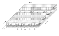
도 1은 본 발명의 반도체 발광 소자를 이용한 디스플레이 장치의 일 실시예를 나타내는 개념도이다.
도 2는 도 1의 A부분의 부분 확대도 이다.
도 3a 및 도 3b는 도 2의 라인 B-B 및 C-C를 따라 절단된 단면도들이다.
도 4는 도 3의 플립 칩 타입 반도체 발광 소자를 나타내는 개념도이다.
도 5a 내지 도 5c는 플립 칩 타입 반도체 발광 소자와 관련하여 컬러를 구현하는 여러 가지 형태를 나타내는 개념도들이다.
도 6은 본 발명의 반도체 발광 소자를 이용한 디스플레이 장치의 제조방법을 나타낸 단면도들이다.
도 7은 발명의 반도체 발광 소자를 이용한 디스플레이 장치의 다른 일 실시예를 나타내는 사시도이다.
도 8은 도 7의 라인 D-D를 따라 절단된 단면도이다.
도 9는 도 8의 수직형 반도체 발광 소자를 나타내는 개념도이다.
도 10은 반도체 발광 소자가 자가 조립 공정에 의해 기판에 조립되는 방법의 일 실시예를 나타내는 도면이다.
도 11은 도 10의 E부분을 확대한 도면이다.
도 12는 반도체 발광 소자를 이용한 디스플레이 장치의 제조 방법에 대해 개략적으로 나타내는 도면이다.
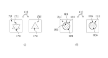
도 13은 복수 개의 형상을 가지는 반도체 발광 소자들을 동시에 기판에 조립하기 위한 일반적인 기판 구조 및 반도체 발광 소자들의 형상을 나타내는 도면이다.
도 14는 복수 개의 형상을 가지는 반도체 발광 소자들을 동시에 기판에 조립하기 위한 본 발명의 기판 구조 및 반도체 발광 소자들의 형상을 나타내는 도면이다.
도 15는 본 발명에 따른 기판 구조 및 반도체 발광 소자의 형상을 구체적으로 나타내는 도면이다.
도 16은 도 15의 기판 구조의 제조 방법 및 상기 기판에 본 발명의 반도체 발광 소자가 조립된 모습을 나타내는 도면이다.
도 17은 본 발명이 종래 기술 대비 가지는 조립 속도의 효과를 표현하는 도면이다.
도 18은 본 발명의 다양한 실시예를 나타내는 도면들이다.1 is a conceptual diagram illustrating an embodiment of a display device using the semiconductor light emitting device of the present invention.
FIG. 2 is a partially enlarged view of portion A of FIG. 1.
3A and 3B are cross-sectional views taken along the lines BB and CC of FIG. 2.
4 is a conceptual diagram illustrating the flip chip type semiconductor light emitting device of FIG. 3.
5A through 5C are conceptual views illustrating various forms of implementing colors in connection with a flip chip type semiconductor light emitting device.
6 is a cross-sectional view illustrating a method of manufacturing a display device using the semiconductor light emitting device of the present invention.
7 is a perspective view showing another embodiment of a display device using the semiconductor light emitting device of the invention.
FIG. 8 is a cross-sectional view taken along the line DD of FIG. 7.
9 is a conceptual diagram illustrating the vertical semiconductor light emitting device of FIG. 8.
10 is a diagram illustrating an embodiment of a method in which a semiconductor light emitting device is assembled to a substrate by a self-assembly process.
FIG. 11 is an enlarged view of a portion E of FIG. 10.
12 is a diagram schematically illustrating a method of manufacturing a display device using a semiconductor light emitting device.
FIG. 13 is a diagram illustrating a general substrate structure and shapes of semiconductor light emitting devices for assembling semiconductor light emitting devices having a plurality of shapes on a substrate at the same time.
14 is a view showing the substrate structure and the shape of the semiconductor light emitting device of the present invention for assembling a plurality of semiconductor light emitting devices having a plurality of shapes at the same time.
15 is a view showing in detail the substrate structure and the shape of the semiconductor light emitting device according to the present invention.
FIG. 16 is a view illustrating a method of manufacturing the substrate structure of FIG. 15 and a state in which the semiconductor light emitting device of the present invention is assembled to the substrate.
17 is a view representing the effect of the assembly speed of the present invention compared to the prior art.
18 is a diagram illustrating various embodiments of the present invention.
이하, 첨부된 도면을 참조하여 본 명세서에 개시된 실시 예를 상세히 설명하되, 도면 부호에 관계없이 동일하거나 유사한 구성요소는 동일한 참조 번호를 부여하고 이에 대한 중복되는 설명은 생략하기로 한다. 이하의 설명에서 사용되는 구성요소에 대한 접미사 "모듈" 및 "부"는 명세서 작성의 용이함만이 고려되어 부여되거나 혼용되는 것으로서, 그 자체로 서로 구별되는 의미 또는 역할을 갖는 것은 아니다. 또한, 본 명세서에 개시된 실시예를 설명함에 있어서 관련된 공지기술에 대한 구체적인 설명이 본 명세서에 개시된 실시 예의 요지를 흐릴 수 있다고 판단되는 경우 그 상세한 설명을 생략한다. 또한, 첨부된 도면은 본 명세서에 개시된 실시 예를 쉽게 이해할 수 있도록 하기 위한 것일 뿐, 첨부된 도면에 의해 본 명세서에 개시된 기술적 사상이 제한되는 것으로 해석되어서는 아니 됨을 유의해야 한다.Hereinafter, embodiments of the present disclosure will be described in detail with reference to the accompanying drawings, and the same or similar components are denoted by the same reference numerals regardless of the reference numerals, and redundant description thereof will be omitted. The suffixes "module" and "unit" for components used in the following description are given or used in consideration of ease of specification, and do not have distinct meanings or roles from each other. In addition, in describing the embodiments disclosed herein, when it is determined that the detailed description of the related known technology may obscure the gist of the embodiments disclosed herein, the detailed description thereof will be omitted. In addition, it should be noted that the accompanying drawings are only for easily understanding the embodiments disclosed in the present specification and are not to be construed as limiting the technical spirit disclosed in the present specification by the accompanying drawings.
나아가, 설명의 편의를 위해 각각의 도면에 대해 설명하고 있으나, 당업자가 적어도 2개 이상의 도면을 결합하여 다른 실시예를 구현하는 것도 본 발명의 권리범위에 속한다.Further, for the convenience of explanation, each of the drawings are described, but those skilled in the art combine at least two or more drawings to implement other embodiments are within the scope of the present invention.
또한, 층, 영역 또는 기판과 같은 요소가 다른 구성요소 "상(on)"에 존재하는 것으로 언급될 때, 이것은 직접적으로 다른 요소 상에 존재하거나 또는 그 사이에 중간 요소가 존재할 수도 있다는 것을 이해할 수 있을 것이다. Also, when an element such as a layer, region or substrate is referred to as being on another component "on", it is to be understood that it may be directly on another element or intermediate elements may be present therebetween. There will be.
본 명세서에서 설명되는 디스플레이 장치는 단위 화소 또는 단위 화소의 집합으로 정보를 표시하는 모든 디스플레이 장치를 포함하는 개념이다. 따라서 완성품에 한정하지 않고 부품에도 적용될 수 있다. 예를 들어 디지털 TV의 일 부품에 해당하는 패널도 독자적으로 본 명세서 상의 디스플레이 장치에 해당한다. 완성품으로는 휴대폰, 스마트 폰(smart phone), 노트북 컴퓨터(laptop computer), 디지털방송용 단말기, PDA(personal digital assistants), PMP(portable multimedia player), 네비게이션, 슬레이트 피씨(Slate PC), Tablet PC, Ultra Book, 디지털 TV, 데스크 탑 컴퓨터 등이 포함될 수 있다. The display device described herein is a concept including all display devices that display information in a unit pixel or a set of unit pixels. Therefore, the present invention can be applied not only to finished products but also to parts. For example, the panel corresponding to one component of the digital TV also corresponds to the display device on this specification. Finished products include mobile phones, smart phones, laptop computers, digital broadcasting terminals, PDAs (personal digital assistants), portable multimedia players (PMPs), navigation, Slate PCs, Tablet PCs, Ultras Books, digital TVs, and desktop computers can be included.
그러나, 본 명세서에 기재된 실시예에 따른 구성은 추후 개발되는 새로운 제품 형태라도, 디스플레이가 가능한 장치에는 적용될 수도 있음을 본 기술 분야의 당업자라면 쉽게 알 수 있을 것이다.However, it will be readily apparent to those skilled in the art that the configuration according to the embodiments described herein may be applied to a device capable of display, even in the form of new products to be developed later.
또한, 당해 명세서에서 언급된 반도체 발광 소자는 LED, 마이크로 LED 등을 포함하는 개념이며, 혼용되어 사용될 수 있다.In addition, the semiconductor light emitting device mentioned in the present specification is a concept including an LED, a micro LED, and the like, and may be used interchangeably.
도 1은 본 발명의 반도체 발광 소자를 이용한 디스플레이 장치의 일실시예를 나타내는 개념도이다.1 is a conceptual diagram illustrating an embodiment of a display device using the semiconductor light emitting device of the present invention.
도 1에 도시된 바와 같이, 디스플레이 장치(100)의 제어부(미도시)에서 처리되는 정보는 플렉서블 디스플레이(flexible display)를 이용하여 표시될 수 있다.As illustrated in FIG. 1, information processed by a controller (not shown) of the
플렉서블 디스플레이는, 예를 들어 외력에 의하여 휘어질 수 있는, 또는 구부러질 수 있는, 또는 비틀어질 수 있는, 또는 접힐 수 있는, 또는 말려질 수 있는 디스플레이를 포함한다.The flexible display includes, for example, a display that can be bent, bent, twisted, or folded, or rolled up by an external force.
나아가, 플렉서블 디스플레이는, 예를 들어 기존의 평판 디스플레이의 디스플레이 특성을 유지하면서, 종이와 같이 휘어지거나, 또는 구부리거나, 또는 접을 수 있거나 또는 말 수 있는 얇고 유연한 기판 위에 제작되는 디스플레이가 될 수 있다.Furthermore, the flexible display can be a display fabricated on a thin, flexible substrate that can be bent, bent, folded, or rolled like paper, for example, while maintaining the display characteristics of a conventional flat panel display.
상기 플렉서블 디스플레이가 휘어지지 않는 상태(예를 들어, 무한대의 곡률반경을 가지는 상태, 이하 제1상태라 한다)에서는 상기 플렉서블 디스플레이의 디스플레이 영역이 평면이 된다. 상기 제1상태에서 외력에 의하여 휘어진 상태(예를 들어, 유한의 곡률 반경을 가지는 상태, 이하, 제2상태라 한다)에서는 상기 디스플레이 영역이 곡면이 될 수 있다. 도 1에 도시된 바와 같이, 상기 제2상태에서 표시되는 정보는 곡면상에 출력되는 시각 정보가 될 수 있다. 이러한 시각 정보는 매트릭스 형태로 배치되는 단위 화소(sub-pixel)의 발광이 독자적으로 제어됨에 의하여 구현된다. 상기 단위 화소는, 예를 들어 하나의 색을 구현하기 위한 최소 단위를 의미한다.In a state where the flexible display is not bent (for example, a state having an infinite curvature radius, hereinafter referred to as a first state), the display area of the flexible display becomes flat. The display area may be a curved surface in a state in which the first state is bent by an external force (for example, a state having a finite radius of curvature, hereinafter referred to as a second state). As shown in FIG. 1, the information displayed in the second state may be visual information output on a curved surface. Such visual information is implemented by independently controlling light emission of a sub-pixel disposed in a matrix form. The unit pixel refers to, for example, a minimum unit for implementing one color.
상기 플렉서블 디스플레이의 단위 화소는 반도체 발광 소자에 의하여 구현될 수 있다. 본 발명에서는 전류를 빛으로 변환시키는 반도체 발광 소자의 일 종류로서 발광 다이오드(Light Emitting Diode: LED)를 예시한다. 상기 발광 다이오드는 작은 크기로 형성되며, 이를 통하여 상기 제2상태에서도 단위 화소의 역할을 할 수 있게 된다.The unit pixel of the flexible display may be implemented by a semiconductor light emitting device. In the present invention, a light emitting diode (LED) is exemplified as a type of semiconductor light emitting device that converts current into light. The light emitting diode is formed to have a small size, thereby enabling it to serve as a unit pixel even in the second state.
상기 발광 다이오드를 이용하여 구현된 플렉서블 디스플레이에 대하여, 이하 도면들을 참조하여 보다 상세히 설명한다.A flexible display implemented using the light emitting diode will be described in more detail with reference to the accompanying drawings.
도 2는 도 1의 A부분의 부분 확대도 이다.FIG. 2 is a partially enlarged view of portion A of FIG. 1.
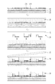
도 3a 및 도 3b는 도 2의 라인 B-B 및 C-C를 따라 절단된 단면도들이다.3A and 3B are cross-sectional views taken along the lines B-B and C-C of FIG. 2.
도 4는 도 3의 플립 칩 타입 반도체 발광 소자를 나타내는 개념도이다.4 is a conceptual diagram illustrating the flip chip type semiconductor light emitting device of FIG. 3.
도 5a 내지 도 5c는 플립 칩 타입 반도체 발광 소자와 관련하여 컬러를 구현하는 여러 가지 형태를 나타내는 개념도들이다.5A through 5C are conceptual views illustrating various forms of implementing colors in connection with a flip chip type semiconductor light emitting device.
도 2, 도 3a 및 도 3b에 도시된 바와 같이, 반도체 발광 소자를 이용한 디스플레이 장치(100)로서 패시브 매트릭스(Passive Matrix, PM) 방식의 반도체 발광 소자를 이용한 디스플레이 장치(100)를 예시한다. 다만, 이하 설명되는 예시는 액티브 매트릭스(Active Matrix, AM) 방식의 반도체 발광 소자에도 적용 가능하다.As shown in FIGS. 2, 3A and 3B, a
도 1에 도시된 디스플레이 장치(100)는, 도 2에 도시된 바와 같이 기판(110), 제1전극(120), 전도성 접착층(130), 제2전극(140) 및 적어도 하나의 반도체 발광 소자(150)를 포함한다.As shown in FIG. 2, the
기판(110)은 플렉서블 기판일 수 있다. 예를 들어, 플렉서블(flexible) 디스플레이 장치를 구현하기 위하여 기판(110)은 유리나 폴리이미드(PI, Polyimide)를 포함할 수 있다. 이외에도 절연성이 있고, 유연성 있는 재질이면, 예를 들어 PEN(Polyethylene Naphthalate), PET(Polyethylene Terephthalate) 등 어느 것이라도 사용될 수 있다. 또한, 상기 기판(110)은 투명한 재질 또는 불투명한 재질 어느 것이나 될 수 있다.The
상기 기판(110)은 제1전극(120)이 배치되는 배선기판이 될 수 있으며, 따라서 상기 제1전극(120)은 기판(110) 상에 위치할 수 있다.The
도 3a에 도시된 바와 같이 절연층(160)은 제1전극(120)이 위치한 기판(110) 상에 배치될 수 있으며, 상기 절연층(160)에는 보조전극(170)이 위치할 수 있다. 이 경우에, 상기 기판(110)에 절연층(160)이 적층된 상태가 하나의 배선기판이 될 수 있다. 보다 구체적으로, 절연층(160)은 폴리이미드(PI, Polyimide), PET, PEN 등과 같이 절연성이 있고, 유연성 있는 재질로, 상기 기판(110)과 일체로 이루어져 하나의 기판을 형성할 수 있다.As shown in FIG. 3A, the insulating
보조전극(170)은 제1전극(120)과 반도체 발광 소자(150)를 전기적으로 연결하는 전극으로서, 절연층(160) 상에 위치하고, 제1전극(120)의 위치에 대응하여 배치된다. 예를 들어, 보조전극(170)은 닷(dot) 형태이며, 절연층(160)을 관통하는 전극홀(171)에 의하여 제1전극(120)과 전기적으로 연결될 수 있다. 상기 전극홀(171)은 비아홀에 도전물질이 채워짐에 의하여 형성될 수 있다.The
도 2 또는 도 3a에 도시된 바와 같이, 절연층(160)의 일면에는 전도성 접착층(130)이 형성되나, 본 발명은 반드시 이에 한정되는 것은 아니다. 예를 들어, 절연층(160)과 전도성 접착층(130)의 사이에 특정 기능을 수행하는 레이어가 형성되거나, 절연층(160)이 없이 전도성 접착층(130)이 기판(110)상에 배치되는 구조도 가능하다. 전도성 접착층(130)이 기판(110)상에 배치되는 구조에서는 전도성 접착층(130)이 절연층의 역할을 할 수 있다.As illustrated in FIG. 2 or 3A, the conductive
상기 전도성 접착층(130)은 접착성과 전도성을 가지는 층이 될 수 있으며, 이를 위하여 상기 전도성 접착층(130)에서는 전도성을 가지는 물질과 접착성을 가지는 물질이 혼합될 수 있다. 또한 전도성 접착층(130)은 연성을 가지며, 이를 통하여 디스플레이 장치에서 플렉서블 기능을 가능하게 한다.The conductive
이러한 예로서, 전도성 접착층(130)은 이방성 전도성 필름(anistropy conductive film, ACF), 이방성 전도 페이스트(paste), 전도성 입자를 함유한 솔루션(solution) 등이 될 수 있다. 상기 전도성 접착층(130)은 두께를 관통하는 Z 방향으로는 전기적 상호 연결을 허용하나, 수평적인 X-Y 방향으로는 전기 절연성을 가지는 레이어로서 구성될 수 있다. 따라서 상기 전도성 접착층(130)은 Z축 전도층으로 명명될 수 있다(다만, 이하 '전도성 접착층'이라 한다).In this example, the conductive
상기 이방성 전도성 필름은 이방성 전도매질(anisotropic conductive medium)이 절연성 베이스부재에 혼합된 형태의 필름으로서, 열 및 압력이 가해지면 특정 부분만 이방성 전도매질에 의하여 전도성을 가지게 된다. 이하, 상기 이방성 전도성 필름에는 열 및 압력이 가해지는 것으로 설명하나, 상기 이방성 전도성 필름이 부분적으로 전도성을 가지기 위하여 다른 방법이 적용될 수도 있다. 전술한 다른 방법은, 예를 들어 상기 열 및 압력 중 어느 하나만이 가해지거나 UV 경화 등이 될 수 있다.The anisotropic conductive film is a film in which an anisotropic conductive medium is mixed with an insulating base member. When the heat and pressure are applied, only the specific portion is conductive by the anisotropic conductive medium. Hereinafter, although the heat and pressure is applied to the anisotropic conductive film, another method may be applied in order for the anisotropic conductive film to have partial conductivity. The other method described above may be, for example, only one of the heat and pressure may be applied, UV curing or the like.
또한, 상기 이방성 전도매질은 예를 들어, 도전볼이나 전도성 입자가 될 수 있다. 예를 들어, 상기 이방성 전도성 필름은 도전볼이 절연성 베이스 부재에 혼합된 형태의 필름으로서, 열 및 압력이 가해지면 특정 부분만 도전볼에 의하여 전도성을 가지게 된다. 이방성 전도성 필름은 전도성 물질의 코어가 폴리머 재질의 절연막에 의하여 피복된 복수의 입자가 함유된 상태가 될 수 있으며, 이 경우에 열 및 압력이 가해진 부분이 절연막이 파괴되면서 코어에 의하여 도전성을 가지게 된다. 이때, 코어의 형태는 변형되어 필름의 두께방향으로 서로 접촉하는 층을 이룰 수 있다. 보다 구체적인 예로서, 열 및 압력은 이방성 전도성 필름에 전체적으로 가해지며, 이방성 전도성 필름에 의하여 접착되는 상대물의 높이 차에 의하여 Z축 방향의 전기적 연결이 부분적으로 형성된다.In addition, the anisotropic conductive medium may be, for example, conductive balls or conductive particles. For example, the anisotropic conductive film is a film in which a conductive ball is mixed with an insulating base member, and when heat and pressure are applied, only a specific portion is conductive by the conductive ball. The anisotropic conductive film may be in a state in which a core of a conductive material contains a plurality of particles coated by an insulating film made of a polymer material, and in this case, a portion to which heat and pressure are applied becomes conductive by the core as the insulating film is destroyed. . At this time, the shape of the core may be deformed to form a layer in contact with each other in the thickness direction of the film. As a more specific example, heat and pressure are applied to the anisotropic conductive film as a whole, and the electrical connection in the Z-axis direction is partially formed by the height difference of the counterpart bonded by the anisotropic conductive film.
다른 예로서, 이방성 전도성 필름은 절연 코어에 전도성 물질이 피복된 복수의 입자가 함유된 상태가 될 수 있다. 이 경우에는 열 및 압력이 가해진 부분이 전도성 물질이 변형되어(눌러 붙어서) 필름의 두께방향으로 전도성을 가지게 된다. 또 다른 예로서, 전도성 물질이 Z축 방향으로 절연성 베이스 부재를 관통하여 필름의 두께방향으로 전도성을 가지는 형태도 가능하다. 이 경우에, 전도성 물질은 뽀족한 단부를 가질 수 있다.As another example, the anisotropic conductive film may be in a state containing a plurality of particles coated with a conductive material on the insulating core. In this case, the portion to which the heat and pressure are applied is deformed (pressed) to have conductivity in the thickness direction of the film. As another example, the conductive material may penetrate the insulating base member in the Z-axis direction and have conductivity in the thickness direction of the film. In this case, the conductive material may have a pointed end.
상기 이방성 전도성 필름은 도전볼이 절연성 베이스 부재의 일면에 삽입된 형태로 구성되는 고정배열 이방성 전도성 필름(fixed array ACF)이 될 수 있다. 보다 구체적으로, 절연성 베이스 부재는 접착성을 가지는 물질로 형성되며, 도전볼은 상기 절연성 베이스 부재의 바닥 부분에 집중적으로 배치되며, 상기 베이스 부재에서 열 및 압력이 가해지면 상기 도전볼과 함께 변형됨에 따라 수직 방향으로 전도성을 가지게 된다.The anisotropic conductive film may be a fixed array anisotropic conductive film (fixed array ACF) consisting of a conductive ball inserted into one surface of the insulating base member. More specifically, the insulating base member is formed of an adhesive material, and the conductive balls are disposed in the bottom portion of the insulating base member, and deforms with the conductive balls when heat and pressure are applied to the base member. Therefore, it has conductivity in the vertical direction.
다만, 본 발명은 반드시 이에 한정되는 것은 아니며, 상기 이방성 전도성 필름은 절연성 베이스 부재에 도전볼이 랜덤하게 혼입된 형태나, 복수의 층으로 구성되며 어느 한 층에 도전볼이 배치되는 형태(double-ACF) 등이 모두 가능하다.However, the present invention is not necessarily limited thereto, and the anisotropic conductive film is a form in which conductive balls are randomly mixed in an insulating base member or a plurality of layers, in which a conductive ball is disposed in one layer (double- ACF) etc. are all possible.
이방성 전도 페이스트는 페이스트와 도전볼의 결합 형태로서, 절연성 및 접착성의 베이스 물질에 도전볼이 혼합된 페이스트가 될 수 있다. 또한, 전도성 입자를 함유한 솔루션은 전도성 파티클 혹은 나노 입자를 함유한 형태의 솔루션이 될 수 있다.The anisotropic conductive paste is a combination of a paste and a conductive ball, and may be a paste in which conductive balls are mixed with an insulating and adhesive base material. In addition, solutions containing conductive particles may be solutions in the form of conductive particles or nanoparticles.
다시 도3a를 참조하면, 제2전극(140)은 보조전극(170)과 이격하여 절연층(160)에 위치한다. 즉, 상기 전도성 접착층(130)은 보조전극(170) 및 제2전극(140)이 위치하는 절연층(160) 상에 배치된다.Referring again to FIG. 3A, the
절연층(160)에 보조전극(170)과 제2전극(140)이 위치된 상태에서 전도성 접착층(130)을 형성한 후에, 반도체 발광 소자(150)를 열 및 압력을 가하여 플립 칩 형태로 접속시키면, 상기 반도체 발광 소자(150)는 제1전극(120) 및 제2전극(140)과 전기적으로 연결된다.After the conductive
도 4를 참조하면, 상기 반도체 발광 소자는 플립 칩 타입(flip chiptype)의 발광 소자가 될 수 있다.Referring to FIG. 4, the semiconductor light emitting device may be a flip chip type light emitting device.
예를 들어, 상기 반도체 발광 소자는 p형 전극(156), p형 전극(156)이 형성되는 p형 반도체층(155), p형 반도체층(155) 상에 형성된 활성층(154), 활성층(154) 상에 형성된 n형 반도체층(153) 및 n형 반도체층(153) 상에서 p형 전극(156)과 수평방향으로 이격 배치되는 n형 전극(152)을 포함한다. 이 경우, p형 전극(156)은 도3에 도시된, 보조전극(170)과 전도성 접착층(130)에 의하여 전기적으로 연결될 수 있고, n형 전극(152)은 제2전극(140)과 전기적으로 연결될 수 있다.For example, the semiconductor light emitting device may include a p-
다시 도 2, 도 3a 및 도 3b를 참조하면, 보조전극(170)은 일방향으로 길게 형성되어, 하나의 보조전극이 복수의 반도체 발광 소자(150)에 전기적으로 연결될 수 있다. 예를 들어, 보조전극을 중심으로 좌우의 반도체 발광 소자들의 p 형 전극들이 하나의 보조전극에 전기적으로 연결될 수 있다.Referring to FIGS. 2, 3A, and 3B, the
보다 구체적으로, 열 및 압력에 의하여 전도성 접착층(130)의 내부로 반도체 발광 소자(150)가 압입되며 이를 통하여 반도체 발광 소자(150)의 p형 전극(156)과 보조전극(170) 사이의 부분과, 반도체 발광 소자(150)의 n형 전극(152)과 제2전극(140) 사이의 부분에서만 전도성을 가지게 되고, 나머지 부분에서는 반도체 발광 소자의 압입이 없어 전도성을 가지지 않게 된다. 이와 같이, 전도성 접착층(130)은 반도체 발광 소자(150)와 보조전극(170) 사이 및 반도체 발광 소자(150)와 제2전극(140) 사이를 상호 결합시켜줄 뿐만 아니라 전기적 연결까지 형성시킨다.More specifically, the semiconductor
또한, 복수의 반도체 발광 소자(150)는 발광 소자 어레이(array)를 구성하며, 발광 소자 어레이에는 형광체층(180)이 형성된다.In addition, the plurality of semiconductor
발광 소자 어레이는 자체 휘도 값이 상이한 복수의 반도체 발광 소자들을 포함할 수 있다. 각각의 반도체 발광 소자(150)는 단위 화소를 구성하며, 제1전극(120)에 전기적으로 연결된다. 예를 들어, 제1전극(120)은 복수 개일 수 있고, 반도체 발광 소자들은 예컨대 수 열로 배치되며, 각 열의 반도체 발광 소자들은 상기 복수 개의 제1전극 중 어느 하나에 전기적으로 연결될 수 있다.The light emitting device array may include a plurality of semiconductor light emitting devices having different luminance values. Each semiconductor
또한, 반도체 발광 소자들이 플립 칩 형태로 접속되므로, 투명 유전체 기판에 성장시킨 반도체 발광 소자들을 이용할 수 있다. 또한, 상기 반도체 발광 소자들은 예컨대 질화물 반도체 발광 소자일 수 있다. 반도체 발광 소자(150)는 휘도가 우수하므로, 작은 크기로도 개별 단위 화소를 구성할 수 있다.In addition, since the semiconductor light emitting devices are connected in a flip chip form, semiconductor light emitting devices grown on a transparent dielectric substrate may be used. In addition, the semiconductor light emitting devices may be, for example, nitride semiconductor light emitting devices. Since the semiconductor
도3에 도시된 바와 같이, 반도체 발광 소자(150)의 사이에 격벽(190)이 형성될 수 있다. 이 경우, 격벽(190)은 개별 단위 화소를 서로 분리하는 역할을 할 수 있으며, 전도성 접착층(130)과 일체로 형성될 수 있다. 예를 들어, 이방성 전도성 필름에 반도체 발광 소자(150)가 삽입됨에 의하여 이방성 전도성 필름의 베이스 부재가 상기 격벽을 형성할 수 있다.As shown in FIG. 3, a
또한, 상기 이방성 전도성 필름의 베이스 부재가 블랙이면, 별도의 블랙 절연체가 없어도 상기 격벽(190)이 반사 특성을 가지는 동시에 대비비(contrast)가 증가될 수 있다.In addition, when the base member of the anisotropic conductive film is black, even when there is no separate black insulator, the
다른 예로서, 상기 격벽(190)으로 반사성 격벽이 별도로 구비될 수 있다. 이 경우에, 상기 격벽(190)은 디스플레이 장치의 목적에 따라 블랙(Black) 또는 화이트(White) 절연체를 포함할 수 있다. 화이트 절연체의 격벽을 이용할 경우 반사성을 높이는 효과가 있을 수 있고, 블랙 절연체의 격벽을 이용할 경우, 반사 특성을 가지는 동시에 대비비(contrast)를 증가시킬 수 있다.As another example, a reflective partition may be separately provided as the
형광체층(180)은 반도체 발광 소자(150)의 외면에 위치할 수 있다. 예를 들어, 반도체 발광 소자(150)는 청색(B) 광을 발광하는 청색 반도체 발광 소자고, 형광체층(180)은 상기 청색(B) 광을 단위 화소의 색상으로 변환시키는 기능을 수행한다. 상기 형광체층(180)은 개별 화소를 구성하는 적색 형광체(181) 또는 녹색 형광체(182)가 될 수 있다.The
즉, 적색의 단위 화소를 이루는 위치에서, 청색 반도체 발광 소자 상에는 청색 광을 적색(R) 광으로 변환시킬 수 있는 적색 형광체(181)가 적층될 수 있고, 녹색의 단위 화소를 이루는 위치에서는, 청색 반도체 발광 소자 상에 청색광을 녹색(G) 광으로 변환시킬 수 있는 녹색 형광체(182)가 적층될 수 있다. 또한, 청색의 단위 화소를 이루는 부분에는 청색 반도체 발광 소자만 단독으로 이용될 수 있다. 이 경우, 적색(R), 녹색(G), 및 청색(B)의 단위 화소들이 하나의 화소를 이룰 수 있다. 보다 구체적으로, 제1전극(120)의 각 라인을 따라 하나의 색상의 형광체가 적층될 수 있다. 따라서, 제1전극(120)에서 하나의 라인은 하나의 색상을 제어하는 전극이 될 수 있다. 즉, 제2전극(140)을 따라서, 적색(R), 녹색(G) 및 청색(B)이 차례로 배치될 수 있으며, 이를 통하여 단위 화소가 구현될 수 있다.That is, a
다만, 본 발명은 반드시 이에 한정되는 것은 아니며, 형광체 대신에 반도체 발광 소자(150)와 퀀텀닷(QD)이 조합되어 적색(R), 녹색(G) 및 청색(B)의 단위 화소들을 구현할 수 있다.However, the present invention is not limited thereto, and instead of the phosphor, the semiconductor
또한, 대비비(contrast) 향상을 위하여 각각의 형광체층들의 사이에는 블랙 매트릭스(191)가 배치될 수 있다. 즉, 이러한 블랙 매트릭스(191)는 명암의 대조를 향상시킬 수 있다.In addition, a
다만, 본 발명은 반드시 이에 한정되는 것은 아니며, 청색, 적색, 녹색을 구현하기 위한 다른 구조가 적용될 수 있다.However, the present invention is not necessarily limited thereto, and other structures for implementing blue, red, and green may be applied.
도 5a를 참조하면, 각각의 반도체 발광 소자(150)는 질화 갈륨(GaN)을 주재료로 하여, 인듐(In) 및/또는 알루미늄(Al)이 함께 첨가되어 청색을 비롯한 다양한 빛을 발광하는 고출력의 발광 소자로 구현될 수 있다.Referring to FIG. 5A, each semiconductor
이 경우, 반도체 발광 소자(150)는 각각 단위 화소(sub-pixel)를 이루기 위하여 적색, 녹색 및 청색 반도체 발광 소자일 수 있다. 예컨대, 적색, 녹색 및 청색 반도체 발광 소자(R, G, B)가 교대로 배치되고, 적색, 녹색 및 청색 반도체 발광 소자에 의하여 적색(Red), 녹색(Green) 및 청색(Blue)의 단위 화소들이 하나의 화소(pixel)를 이루며, 이를 통하여 풀 칼라 디스플레이가 구현될 수 있다.In this case, the semiconductor
도 5b를 참조하면, 반도체 발광 소자(150a)는 황색 형광체층이 개별 소자 마다 구비된 백색 발광 소자(W)를 구비할 수 있다. 이 경우에는, 단위 화소를 이루기 위하여, 백색 발광 소자(W) 상에 적색 형광체층(181), 녹색 형광체층(182), 및 청색 형광체층(183)이 구비될 수 있다. 또한, 이러한 백색 발광 소자(W) 상에 적색, 녹색, 및 청색이 반복되는 컬러 필터를 이용하여 단위 화소를 이룰 수 있다.Referring to FIG. 5B, the semiconductor
도 5c를 참조하면, 자외선 발광 소자(150b) 상에 적색 형광체층(184), 녹색 형광체층(185), 및 청색 형광체층(186)이 구비되는 구조도 가능하다. 이와 같이, 반도체 발광 소자는 가시광선뿐만 아니라 자외선(UV)까지 전 영역에 사용 가능하며, 자외선(UV)이 상부 형광체의 여기원(excitation source)으로 사용 가능한 반도체 발광 소자의 형태로 확장될 수 있다.Referring to FIG. 5C, the
본 예시를 다시 살펴보면, 반도체 발광 소자는 전도성 접착층 상에 위치되어, 디스플레이 장치에서 단위 화소를 구성한다. 반도체 발광 소자는 휘도가 우수하므로, 작은 크기로도 개별 단위 화소를 구성할 수 있다.Referring back to the present example, the semiconductor light emitting device is positioned on the conductive adhesive layer to constitute a unit pixel in the display device. Since the semiconductor light emitting device is excellent in brightness, individual unit pixels can be configured with a small size.
이와 같은 개별 반도체 발광 소자(150)의 크기는 예를 들어, 한 변의 길이가 80㎛ 이하일 수 있고, 직사각형 또는 정사각형 소자일 수 있다. 직사각형인 경우에는 20 X 80㎛ 이하의 크기가 될 수 있다.The size of the individual semiconductor
또한, 한 변의 길이가 10㎛인 정사각형의 반도체 발광 소자(150)를 단위 화소로 이용하여도 디스플레이 장치를 이루기 위한 충분한 밝기가 나타난다.In addition, even when a square semiconductor
따라서, 단위 화소의 크기가 한 변이 600㎛, 나머지 한 변이 300㎛인 직사각형 화소인 경우를 예로 들면, 반도체 발광 소자의 거리가 상대적으로 충분히 크게 된다.Therefore, for example, when the size of the unit pixel is a rectangular pixel in which one side is 600 µm and the other side is 300 µm, the distance of the semiconductor light emitting element is relatively large.
따라서, 이러한 경우, HD화질 이상의 고화질을 가지는 플렉서블 디스플레이 장치를 구현할 수 있게 된다.Therefore, in this case, it is possible to implement a flexible display device having a high picture quality of HD or more.
상기에서 설명된 반도체 발광 소자를 이용한 디스플레이 장치는 새로운 형태의 제조방법에 의하여 제조될 수 있다. 이하, 도 6을 참조하여 상기 제조 방법에 대하여 설명한다.The display device using the semiconductor light emitting device described above may be manufactured by a new type of manufacturing method. Hereinafter, the manufacturing method will be described with reference to FIG. 6.
도 6은 본 발명의 반도체 발광 소자를 이용한 디스플레이 장치의 제조 방법을 나타낸 단면도들이다.6 is a cross-sectional view illustrating a method of manufacturing a display device using the semiconductor light emitting device of the present invention.
도 6에 도시된 바와 같이, 먼저, 보조전극(170) 및 제2전극(140)이 위치된 절연층(160) 상에 전도성 접착층(130)을 형성한다. 배선기판(110)에 절연층(160)이 적층되며, 상기 배선기판(110)에는 제1전극(120), 보조전극(170) 및 제2전극(140)이 배치된다. 이 경우에, 제1전극(120)과 제2전극(140)은 상호 직교 방향으로 배치될 수 있다. 또한, 플렉서블(flexible) 디스플레이 장치를 구현하기 위하여 배선기판(110) 및 절연층(160)은 각각 유리 또는 폴리이미드(PI)를 포함할 수 있다.As shown in FIG. 6, first, the conductive
상기 전도성 접착층(130)은 예를 들어, 이방성 전도성 필름에 의하여 구현될 수 있으며, 이를 위하여 절연층(160)이 위치된 기판에 이방성 전도성 필름이 도포될 수 있다.The conductive
다음에, 보조전극(170) 및 제2전극(140)들의 위치에 대응하고, 개별 화소를 구성하는 복수의 반도체 발광 소자(150)가 위치된 임시기판(112)을, 상기 반도체 발광 소자(150)가 보조전극(170) 및 제2전극(140)와 마주하도록 배치한다.Next, the semiconductor
이 경우에, 임시기판(112)은 반도체 발광 소자(150)를 성장시키는 성장 기판으로서, 사파이어(spire) 기판 또는 실리콘(silicon) 기판이 될 수 있다.In this case, the
상기 반도체 발광 소자는 웨이퍼(wafer) 단위로 형성될 때, 디스플레이 장치를 이룰 수 있는 간격 및 크기를 가지도록 함으로써, 디스플레이 장치에 효과적으로 이용될 수 있다.When the semiconductor light emitting device is formed in a wafer unit, the semiconductor light emitting device may be effectively used in the display device by having a gap and a size capable of forming the display device.
그 다음에, 배선기판과 임시기판(112)을 열 압착한다. 예를 들어, 배선기판과 임시기판(112)은 ACF 프레스 헤드를 적용하여 열 압착할 수 있다. 상기 열 압착에 의하여 배선기판과 임시기판(112)은 본딩(bonding)된다. 열 압착에 의하여 전도성을 갖는 이방성 전도성 필름의 특성에 의해 반도체 발광 소자(150)와 보조전극(170) 및 제2전극(140)의 사이의 부분만 전도성을 가지게 되며, 이를 통하여 전극들과 반도체 발광 소자(150)는 전기적으로 연결될 수 있다. 이 때에, 반도체 발광 소자(150)가 상기 이방성 전도성 필름의 내부로 삽입되며, 이를 통하여 반도체 발광 소자(150) 사이에 격벽이 형성될 수 있다.Next, the wiring board and the
그 다음에, 상기 임시기판(112)을 제거한다. 예를 들어, 임시기판(112)은 레이저 리프트 오프법(Laser Lift-off, LLO) 또는 화학적 리프트 오프법(Chemical Lift-off, CLO)을 이용하여 제거할 수 있다.Then, the
마지막으로, 상기 임시기판(112)을 제거하여 반도체 발광 소자들(150)을 외부로 노출시킨다. 필요에 따라, 반도체 발광 소자(150)가 결합된 배선기판 상을 실리콘 옥사이드(SiOx) 등을 코팅하여 투명 절연층(미도시)을 형성할 수 있다.Finally, the
또한, 상기 반도체 발광 소자(150)의 일 면에 형광체층을 형성하는 단계를 더 포함할 수 있다. 예를 들어, 반도체 발광 소자(150)는 청색(B) 광을 발광하는 청색 반도체 발광 소자고, 이러한 청색(B) 광을 단위 화소의 색상으로 변환시키기 위한 적색 형광체 또는 녹색 형광체가 상기 청색 반도체 발광 소자의 일면에 레이어를 형성할 수 있다.In addition, the method may further include forming a phosphor layer on one surface of the semiconductor
이상에서 설명된 반도체 발광 소자를 이용한 디스플레이 장치의 제조 방법이나 구조는 여러 가지 형태로 변형될 수 있다. 그 예로서, 상기에서 설명된 디스플레이 장치에는 수직형 반도체 발광 소자도 적용될 수 있다.The manufacturing method or structure of the display device using the semiconductor light emitting device described above may be modified in various forms. As an example, a vertical semiconductor light emitting device may also be applied to the display device described above.
또한, 이하 설명되는 변형예 또는 실시예에서는 앞선 예와 동일 또는 유사한 구성에 대해서는 동일, 유사한 참조번호가 부여되고, 그 설명은 처음 설명으로 갈음된다.In addition, in the modification or embodiment described below, the same or similar reference numerals are assigned to the same or similar configuration as the previous example, and the description is replaced with the first description.
도 7은 본 발명의 반도체 발광 소자를 이용한 디스플레이 장치의 다른 일 실시예를 나타내는 사시도이고, 도 8은 도 7의 라인 D-D를 따라 취한 단면도이며, 도 9은 도 8의 수직형 반도체 발광 소자를 나타내는 개념도이다.7 is a perspective view illustrating another embodiment of a display device using the semiconductor light emitting device of the present invention, FIG. 8 is a cross-sectional view taken along the line DD of FIG. 7, and FIG. 9 is a view showing the vertical semiconductor light emitting device of FIG. 8. Conceptual diagram.
본 도면들을 참조하면, 디스플레이 장치는 패시브 매트릭스(Passive Matrix, PM) 방식의 수직형 반도체 발광 소자를 이용한 디스플레이 장치가 될 수 있다.Referring to the drawings, the display device may be a display device using a passive semiconductor light emitting device of a passive matrix (PM) type.
상기 디스플레이 장치는 기판(210), 제1전극(220), 전도성 접착층(230), 제2전극(240) 및 적어도 하나의 반도체 발광 소자(250)를 포함한다.The display device includes a
기판(210)은 제1전극(220)이 배치되는 배선기판으로서, 플렉서블(flexible) 디스플레이 장치를 구현하기 위하여 폴리이미드(PI)를 포함할 수 있다. 이외에도 절연성이 있고, 유연성 있는 재질이면 어느 것이라도 사용 가능할 것이다.The
제1전극(220)은 기판(210) 상에 위치하며, 일 방향으로 긴 바(bar) 형태의 전극으로 형성될 수 있다. 상기 제1 전극(220)은 데이터 전극의 역할을 하도록 이루어질 수 있다.The
전도성 접착층(230)은 제1전극(220)이 위치하는 기판(210)상에 형성된다. 플립 칩 타입(flip chip type)의 발광 소자가 적용된 디스플레이 장치와 같이, 전도성 접착층(230)은 이방성 전도성 필름(Anisotropy Conductive Film, ACF), 이방성 전도 페이스트(paste), 전도성 입자를 함유한 솔루션(solution) 등이 될 수 있다. 다만, 본 실시 예에서도 이방성 전도성 필름에 의하여 전도성 접착층(230)이 구현되는 경우를 예시한다.The conductive
기판(210) 상에 제1전극(220)이 위치하는 상태에서 이방성 전도성 필름을 위치시킨 후에, 반도체 발광 소자(250)를 열 및 압력을 가하여 접속시키면, 상기 반도체 발광 소자(250)가 제1전극(220)과 전기적으로 연결된다. 이 때, 상기 반도체 발광 소자(250)는 제1전극(220) 상에 위치되도록 배치되는 것이 바람직하다.After placing the anisotropic conductive film in a state where the
상기 전기적 연결은 전술한 바와 같이, 이방성 전도성 필름에서 열 및 압력이 가해지면 부분적으로 두께방향으로 전도성을 가지기 때문에 생성된다. 따라서, 이방성 전도성 필름에서는 두께 방향으로 전도성을 가지는 부분과 전도성을 가지지 않는 부분으로 구획된다.The electrical connection is created because, as described above, in the anisotropic conductive film is partially conductive in the thickness direction when heat and pressure are applied. Therefore, in the anisotropic conductive film, it is divided into a portion having conductivity and a portion having no conductivity in the thickness direction.
또한, 이방성 전도성 필름은 접착 성분을 함유하기 때문에, 전도성 접착층(230)은 반도체 발광 소자(250)와 제1전극(220) 사이에서 전기적 연결뿐만 아니라 기계적 결합까지 구현한다.In addition, since the anisotropic conductive film contains an adhesive component, the conductive
이와 같이, 반도체 발광 소자(250)는 전도성 접착층(230) 상에 위치되며, 이를 통하여 디스플레이 장치에서 개별 화소를 구성한다. 반도체 발광 소자(250)는 휘도가 우수하므로, 작은 크기로도 개별 단위 픽셀을 구성할 수 있다. 이와 같은 개별 반도체 발광 소자(250)의 크기는 예를 들어, 한 변의 길이가 80㎛ 이하일 수 있고, 직사각형 또는 정사각형 소자일 수 있다. 직사각형인 경우에는 예를 들어, 20 X 80㎛ 이하의 크기가 될 수 있다.As such, the semiconductor
상기 반도체 발광 소자(250)는 수직형 구조가 될 수 있다. The semiconductor
수직형 반도체 발광 소자들의 사이에는, 제1전극(220)의 길이 방향과 교차하는 방향으로 배치되고, 수직형 반도체 발광 소자(250)와 전기적으로 연결된 복수의 제2전극(240)이 위치한다.Between the vertical semiconductor light emitting devices, a plurality of
도 9를 참조하면, 이러한 수직형 반도체 발광 소자(250)는 p형 전극(256), p형 전극(256) 상에 형성된 p형 반도체층(255), p형 반도체층(255) 상에 형성된 활성층(254), 활성층(254)상에 형성된 n형 반도체층(253) 및 n형 반도체층(253) 상에 형성된 n형 전극(252)을 포함한다. 이 경우, 하부에 위치한 p형 전극(256)은 제1전극(220)과 전도성 접착층(230)에 의하여 전기적으로 연결될 수 있고, 상부에 위치한 n형 전극(252)은 후술하는 제2전극(240)과 전기적으로 연결될 수 있다. 이러한 수직형 반도체 발광 소자(250)는 전극을 상/하로 배치할 수 있으므로, 칩 사이즈를 줄일 수 있다는 큰 강점을 가지고 있다.Referring to FIG. 9, the vertical semiconductor
다시 도 8을 참조하면, 상기 반도체 발광 소자(250)의 일면에는 형광체층(280)이 형성될 수 있다. 예를 들어, 반도체 발광 소자(250)는 청색(B) 광을 발광하는 청색 반도체 발광 소자(251)이고, 이러한 청색(B) 광을 단위 화소의 색상으로 변환시키기 위한 형광체층(280)이 구비될 수 있다. 이 경우에, 형광체층(280)은 개별 화소를 구성하는 적색 형광체(281) 및 녹색 형광체(282) 일 수 있다.Referring back to FIG. 8, a
즉, 적색의 단위 화소를 이루는 위치에서, 청색 반도체 발광 소자 상에는 청색 광을 적색(R) 광으로 변환시킬 수 있는 적색 형광체(281)가 적층될 수 있고, 녹색의 단위 화소를 이루는 위치에서는, 청색 반도체 발광 소자 상에 청색광을 녹색(G) 광으로 변환시킬 수 있는 녹색 형광체(282)가 적층될 수 있다. 또한, 청색의 단위 화소를 이루는 부분에는 청색 반도체 발광 소자만 단독으로 이용될 수 있다. 이 경우, 적색(R), 녹색(G), 및 청색(B)의 단위 화소들이 하나의 화소를 이룰 수 있다.That is, a
다만, 본 발명은 반드시 이에 한정되는 것은 아니며, 플립 칩 타입(flip chip type)의 발광 소자가 적용된 디스플레이 장치에서 전술한 바와 같이, 청색, 적색, 녹색을 구현하기 위한 다른 구조가 적용될 수 있다.However, the present invention is not necessarily limited thereto, and as described above in the display device to which the flip chip type light emitting device is applied, other structures for implementing blue, red, and green may be applied.
다시 본 실시예를 살펴보면, 제2전극(240)은 반도체 발광 소자들(250) 사이에 위치하고, 반도체 발광 소자들(250)과 전기적으로 연결된다. 예를 들어, 반도체 발광 소자들(250)은 복수의 열로 배치되고, 제2전극(240)은 반도체 발광 소자들(250)의 열들 사이에 위치할 수 있다.Referring back to the present embodiment, the
개별 화소를 이루는 반도체 발광 소자(250) 사이의 거리가 충분히 크기 때문에 제2전극(240)은 반도체 발광 소자들(250) 사이에 위치될 수 있다.Since the distance between the semiconductor
제2전극(240)은 일 방향으로 긴 바(bar) 형태의 전극으로 형성될 수 있으며, 제1전극과 상호 수직한 방향으로 배치될 수 있다.The
또한, 제2전극(240)과 반도체 발광 소자(250)는 제2전극(240)에서 돌출된 연결 전극에 의해 전기적으로 연결될 수 있다. 보다 구체적으로, 상기 연결 전극이 반도체 발광 소자(250)의 n형 전극이 될 수 있다. 예를 들어, n형 전극은 오믹(ohmic) 접촉을 위한 오믹 전극으로 형성되며, 상기 제2전극은 인쇄 또는 증착에 의하여 오믹 전극의 적어도 일부를 덮게 된다. 이를 통하여 제2전극(240)과 반도체 발광 소자(250)의 n형 전극이 전기적으로 연결될 수 있다.In addition, the
다시 도 8을 참조하면, 상기 제2전극(240)은 전도성 접착층(230) 상에 위치될 수 있다. 경우에 따라, 반도체 발광 소자(250)가 형성된 기판(210) 상에 실리콘 옥사이드(SiOx) 등을 포함하는 투명 절연층(미도시)이 형성될 수 있다. 투명 절연층이 형성된 후에 제2전극(240)을 위치시킬 경우, 상기 제2전극(240)은 투명 절연층 상에 위치하게 된다. 또한, 제2전극(240)은 전도성 접착층(230) 또는 투명 절연층에 이격되어 형성될 수도 있다.Referring to FIG. 8 again, the
만약 반도체 발광 소자(250) 상에 제2전극(240)을 위치시키기 위하여는 ITO(Indium Tin Oxide)와 같은 투명 전극을 사용한다면, ITO 물질은 n형 반도체층과는 접착성이 좋지 않은 문제가 있다. 따라서, 본 발명은 반도체 발광 소자(250) 사이에 제2전극(240)을 위치시킴으로써, ITO와 같은 투명 전극을 사용하지 않아도 되는 이점이 있다. 따라서, 투명한 재료 선택에 구속되지 않고, n형 반도체층과 접착성이 좋은 전도성 물질을 수평 전극으로 사용하여 광추출 효율을 향상시킬 수 있다.If a transparent electrode such as indium tin oxide (ITO) is used to position the
다시 도 8을 참조하면, 반도체 발광 소자(250) 사이에는 격벽(290)이 위치할 수 있다. 즉, 개별 화소를 이루는 반도체 발광 소자(250)를 격리시키기 위하여 수직형 반도체 발광 소자(250) 사이에는 격벽(290)이 배치될 수 있다. 이 경우, 격벽(290)은 개별 단위 화소를 서로 분리하는 역할을 할 수 있으며, 상기 전도성 접착층(230)과 일체로 형성될 수 있다. 예를 들어, 이방성 전도성 필름에 반도체 발광 소자(250)가 삽입됨에 의하여 이방성 전도성 필름의 베이스부재가 상기 격벽을 형성할 수 있다.Referring back to FIG. 8,
또한, 상기 이방성 전도성 필름의 베이스 부재가 블랙이면, 별도의 블랙 절연체가 없어도 상기 격벽(290)이 반사 특성을 가지는 동시에 대비비(contrast)가 증가될 수 있다.In addition, when the base member of the anisotropic conductive film is black, even if there is no separate black insulator, the
다른 예로서, 상기 격벽(190)으로서, 반사성 격벽이 별도로 구비될 수 있다. 격벽(290)은 디스플레이 장치의 목적에 따라 블랙(Black) 또는 화이트(White) 절연체를 포함할 수 있다.As another example, as the
만일 제2전극(240)이 반도체 발광 소자(250) 사이의 전도성 접착층(230) 상에 바로 위치된 경우, 격벽(290)은 수직형 반도체 발광 소자(250) 및 제2전극(240)의 사이 사이에 위치될 수 있다. 따라서, 반도체 발광 소자(250)를 이용하여 작은 크기로도 개별 단위 픽셀을 구성할 수 있고, 반도체 발광 소자(250)의 거리가 상대적으로 충분히 크게 되어 제2전극(240)을 반도체 발광 소자(250) 사이에 위치시킬 수 있고, HD 화질을 가지는 플렉서블 디스플레이 장치를 구현할 수 있는 효과가 있게 된다.If the
또한, 도8에 도시된 바와 같이, 대비비(contrast) 향상을 위하여 각각의 형광체 사이에는 블랙 매트릭스(291)가 배치될 수 있다. 즉, 이러한 블랙 매트릭스(291)는 명암의 대조를 향상시킬 수 있다.In addition, as shown in FIG. 8, a
도 10은 반도체 발광 소자가 자가 조립 공정에 의해 기판에 조립되는 방법의 일 실시예를 나타내는 도면이다.10 is a diagram illustrating an embodiment of a method in which a semiconductor light emitting device is assembled to a substrate by a self-assembly process.
또한, 도 11은 도 10의 E부분을 확대한 도면이다.FIG. 11 is an enlarged view of a portion E of FIG. 10.
도 10과 도 11를 참조하면, 반도체 발광 소자(1050)는 유체(1020)가 채워진 챔버(1030)에 투입될 수 있다.10 and 11, the semiconductor
이 후, 조립 기판(1010)이 챔버(1030) 상에 배치될 수 있다. 실시 예에 따라, 조립 기판(1010)은 챔버(1030) 내로 투입될 수도 있다. 이때 조립 기판(1010)이 투입되는 방향은 상기 조립 기판(1010)의 조립 홈(1011)이 유체(1020)를 마주보는 방향이다.Thereafter, the
조립 기판(1010)에는 조립될 반도체 발광 소자(1050) 각각에 대응하는 한 쌍의 전극(1012,1013)이 형성될 수 있다. 상기 전극(1012,1013)은 투명 전극(ITO)으로 구현되거나, 기타 일반적인 재료를 이용해 구현될 수 있다. 상기 전극(1012,1013)은 전압이 인가됨에 따라 전기장을 생성함으로써, 조립 홈(1012,1013)에 접촉한 반도체 발광 소자(1050)를 안정적으로 고정시키는 조립 전극에 해당한다. A pair of
구체적으로 상기 전극(1012,1013)에는 교류 전압이 인가될 수 있으며, 상기 전극(1012,1013) 주변부에는 부유하는 반도체 발광 소자(1050)는 유전 분극에 의해 극성을 가질 수 있다. 또한, 유전 분극된 반도체 발광 소자의 경우, 상기 전극(1012,1013) 주변부에 형성되는 불균일한 전기장에 의해 특정 방향으로 이동되거나 고정될 수 있다. 이를 유전 영동이라 하며, 본 발명의 자가 조립 공정에서, 상기 유전 영동을 이용하여 조립 홈(1011)에 반도체 발광 소자(1050)를 안정적으로 고정할 수 있다.In detail, an AC voltage may be applied to the
또한, 상기 조립 전극(1012,1013)간의 간격은 예를 들어, 반도체 발광 소자(1050)의 너비 및 조립 홈(1011)의 직경보다 작게 형성되어, 전기장을 이용한 반도체 발광 소자(1050)의 조립 위치를 보다 정밀하게 고정할 수 있다.In addition, the distance between the
또한, 상기 조립 전극(1012,1013) 상에는 절연층(1014)이 형성되어, 전극(1012,1013)을 유체(1020)로부터 보호하고, 상기 조립 전극(1012,1013)에 흐르는 전류의 누출을 방지할 수 있다. 예컨대, 절연층(1014)은 실리카, 알루미나 등의 무기물 절연체 또는 유기물 절연체가 단일층 또는 다층으로 형성될 수 있다. 또한, 절연층(1014)은 반도체 발광 소자(1050) 조립 시 상기 조립 전극(1012,1013)의 손상을 방지하기 위한 최소 두께를 가질 수 있고, 상기 반도체 발광 소자(1050)가 안정적으로 조립되기 위한 최대 두께를 가질 수 있다.In addition, an insulating
절연층(1014)의 상부에는 격벽(1015)이 형성될 수 있다. 상기 격벽(1015)의 일부 영역은 상기 조립 전극(1012,1013)의 상부에 위치하고, 나머지 영역은 상기 조립 기판(1010)의 상부에 위치할 수 있다.A
예컨대, 조립 기판(1010)의 제조 시, 절연층(1014) 상부 전체에 형성된 격벽 중 일부가 제거됨으로써, 반도체 발광 소자(1050)들 각각이 상기 조립 기판(1010)에 결합되는 조립 홈(1011)이 형성될 수 있다.For example, when fabricating the
도 11에 도시된 바와 같이, 상기 조립 기판(1010)에는 반도체 발광 소자(1050)가 결합되는 조립 홈(1011)이 형성되고, 상기 조립 홈(1011)이 형성된 면은 유체(1020)와 접촉할 수 있다. 상기 조립 홈(1011)은 반도체 발광 소자(1050)의 정확한 조립 위치를 가이드할 수 있다.As shown in FIG. 11, an
한편, 상기 조립 홈(1011)은 조립되는 반도체 발광 소자(1050)의 형상에 대응하는 형상 및 크기를 가질 수 있다. 이에 따라, 조립 홈(1011)에 다른 반도체 발광 소자가 조립되거나 복수의 반도체 발광 소자들이 조립되는 것을 방지할 수 있다.Meanwhile, the
또한 상기 조립 홈(1011)의 깊이는, 상기 반도체 발광 소자(1050)의 세로 높이보다 작게 형성할 수 있다. 이를 통해 상기 반도체 발광 소자(1050)는 격벽(1015)들 사이로 돌출되는 구조를 가질 수 있고, 조립 이후 발생할 수 있는 전사 과정에서 전사 기판의 돌기부와 쉽게 접촉할 수 있다. In addition, the depth of the
또한, 도 10에 도시된 바와 같이, 조립 기판(1010)이 배치된 후, 자성체를 포함하는 조립 장치(1040)가 상기 조립 기판(1010)을 따라 이동할 수 있다. 상기 조립 장치(1040)는 자기장이 미치는 영역을 유체(1020) 내로 최대화하기 위해, 조립 기판(1010)과 접촉한 상태로 이동할 수 있다. 예를 들어, 조립 장치(1040)는 복수의 자성체를 포함하거나, 조립 기판(1010)과 대응하는 크기의 자성체를 포함할 수도 있다. 이 경우, 조립 장치(1040)의 이동 거리는 소정 범위 이내로 제한될 수도 있다.In addition, as shown in FIG. 10, after the
조립 장치(1040)에 의해 발생하는 자기장에 의해, 챔버(1030) 내의 반도체 발광 소자(1050)는 조립 장치(1040)를 향해 이동할 수 있다.The magnetic field generated by the
반도체 발광 소자(1050)는 조립 장치(1040)를 향해 이동 중, 도 11에 도시된 바와 같이, 조립 홈(1011)으로 진입하여 조립 기판(1010)과 접촉될 수 있다. While moving toward the
또한 상기 반도체 발광 소자(1050)는 자가 조립 공정이 수행될 수 있도록, 상기 반도체 발광 소자 내부에 자성층을 포함할 수 있다. In addition, the semiconductor
한편, 조립 기판(1010)의 조립 전극(1012,1013)에 의해 생성된 전기장으로 인해, 조립 기판(1010)에 접촉된 반도체 발광 소자(1050)는 조립 장치(1040)의 이동에 의해 이탈되는 현상을 방지할 수 있다.Meanwhile, due to the electric fields generated by the
따라서, 도 10및 도 11에 도시한 전자기장을 이용한 자가 조립 방식에 의해, 복수 개의 반도체 발광 소자(1050)들은 동시 다발적으로 상기 조립 기판(1010)에 조립된다. Accordingly, by the self-assembly method using the electromagnetic fields shown in FIGS. 10 and 11, the plurality of semiconductor
도 12는 반도체 발광 소자를 이용한 디스플레이 장치의 제조 방법에 대해 개략적으로 나타내는 도면이다.12 is a diagram schematically illustrating a method of manufacturing a display device using a semiconductor light emitting device.
먼저 성장 기판에서 반도체 발광 소자들을 형성한다(S1210). 상기 반도체 발광 소자들은 제 1도전형 반도체층, 활성층, 제 2도전형 반도체층을 포함할 수 있다. 또한 상기 제 1도전형 반도체층 상에 형성되는 제 1도전형 전극 및 제 2도전형 반도체층 상에 형성되는 제 2도전형 전극이 더 포함될 수 있다. First, semiconductor light emitting devices are formed on a growth substrate (S1210). The semiconductor light emitting devices may include a first conductive semiconductor layer, an active layer, and a second conductive semiconductor layer. In addition, a first conductive electrode formed on the first conductive semiconductor layer and a second conductive electrode formed on the second conductive semiconductor layer may be further included.
상기 반도체 발광 소자들은 수평형 반도체 발광 소자 또는 수직형 반도체 발광 소자 모두 가능하나, 수직형 반도체 발광 소자의 경우, 상기 제1도전형 전극과 상기 제 2도전형 전극은 마주보는 구조이기 때문에, 성장기판에서 반도체 발광 소자를 분리하고, 후속 공정에서 일단의 도전형 전극을 형성하는 공정을 추가한다. 또한 전술하였듯이 자가 조립 공정을 위해서는 반도체 발광 소자에 자성층이 포함되어야 한다. The semiconductor light emitting device may be a horizontal semiconductor light emitting device or a vertical semiconductor light emitting device, but in the case of a vertical semiconductor light emitting device, since the first conductive electrode and the second conductive electrode face each other, a growth substrate is provided. The semiconductor light emitting device is separated, and a step of forming a conductive electrode in a subsequent step is added. In addition, as described above, a magnetic layer should be included in the semiconductor light emitting device for the self-assembly process.
상기 반도체 발광 소자들을 디스플레이 장치에 활용하기 위해서는 일반적으로 Red, Green, Blue에 해당하는 색상을 발광하는 3가지 종류의 반도체 발광 소자들이 필요하다. 하나의 성장 기판에는 하나의 색상을 발광하는 반도체 발광 소자들이 형성되므로, 상기 3가지 종류의 반도체 발광 소자들을 이용하여 개별 단위 화소를 구현하는 디스플레이 장치를 위해서는 별도의 기판이 요구된다. 따라서, 개별 반도체 발광 소자들은 성장 기판에서 분리되어 최종 기판에 조립 또는 전사되어야 한다. 상기 최종 기판은 반도체 발광 소자가 발광할 수 있도록 상기 반도체 발광 소자에 전압을 인가하는 배선 전극이 형성되는 공정이 수행되는 기판이다.In order to utilize the semiconductor light emitting devices in a display device, three types of semiconductor light emitting devices that emit colors corresponding to red, green, and blue are generally required. Since a semiconductor light emitting device emitting one color is formed on one growth substrate, a separate substrate is required for a display device implementing individual unit pixels using the three types of semiconductor light emitting devices. Thus, individual semiconductor light emitting devices must be separated from the growth substrate and assembled or transferred to the final substrate. The final substrate is a substrate on which a wiring electrode for applying a voltage to the semiconductor light emitting device is formed so that the semiconductor light emitting device can emit light.
따라서 각 색상을 발광하는 반도체 발광 소자들은 일단 전사 기판 또는 조립 기판으로 이동한 후(S1220) 최종 기판으로 다시 전사될 수 있다. 경우에 따라 상기 전사 기판 또는 조립 기판에 배선 공정을 수행하는 경우, 상기 전사 기판 또는 조립 기판은 최종 기판으로서 역할을 수행한다.Therefore, the semiconductor light emitting devices emitting each color may be transferred back to the final substrate after moving to the transfer substrate or the assembly substrate (S1220). In some cases, when a wiring process is performed on the transfer substrate or the assembly substrate, the transfer substrate or the assembly substrate serves as a final substrate.
전사 기판 또는 조립 기판에 반도체 발광 소자가 배치(S1220)되는 방법은 크게 3가지로 나뉠 수 있다.The method of disposing a semiconductor light emitting device on a transfer substrate or an assembly substrate (S1220) may be largely divided into three methods.
첫째, 스탬프 공정에 의해 성장 기판에서 전사 기판으로 반도체 발광 소자를 이동하는 방법이다(S1221). 스탬프 공정이란 접착력이 있는 돌기부를 지닌 유연한 소재의 기판을 이용하여, 상기 돌기부를 통해 성장 기판에서 반도체 발광 소자를 분리하는 공정을 말한다. 돌기부의 간격 및 배치를 조절하여 성장 기판의 반도체 발광 소자를 선택적으로 분리할 수 있다. First, a method of moving a semiconductor light emitting device from a growth substrate to a transfer substrate by a stamp process (S1221). The stamping process refers to a process of separating a semiconductor light emitting device from a growth substrate through the protrusion by using a substrate of a flexible material having an adhesive protrusion. The semiconductor light emitting device of the growth substrate may be selectively separated by adjusting the spacing and arrangement of the protrusions.
두번째로, 전술하였듯이 자가 조립 공정을 이용하여 반도체 발광 소자를 조립 기판에 조립하는 방법이다(S1222). 자가 조립 공정을 위해서는 반도체 발광 소자가 성장 기판으로부터 분리되어 낱개로 존재해야 하는 바, 필요한 반도체 발광 소자의 수만큼 레이저 리프트 오프(LLO) 공정 등을 통해 상기 반도체 발광 소자들을 성장 기판으로부터 분리시킨다. 이후 상기 반도체 발광 소자들을 유체 내에 분산하고 전자기장을 이용하여 조립 기판에 조립한다. Secondly, as described above, the semiconductor light emitting device is assembled to the assembly substrate using the self-assembly process (S1222). For the self-assembly process, the semiconductor light emitting devices must be separated from the growth substrate, and thus the semiconductor light emitting devices are separated from the growth substrate by the laser lift-off (LLO) process. Thereafter, the semiconductor light emitting devices are dispersed in a fluid and assembled to an assembly board using an electromagnetic field.
상기 자가 조립 공정은 하나의 조립 기판에 R,G,B 색상을 구현하는 각각의 반도체 발광 소자들을 동시에 조립하거나, 개별 조립 기판을 통해 개별 색상의 반도체 발광 소자를 조립할 수 있다.The self-assembly process may simultaneously assemble each semiconductor light emitting device that implements R, G, and B colors on one assembly board, or assemble semiconductor light emitting devices of individual colors through the individual assembly boards.
세번째로는, 상기 스탬프 공정과 자가 조립 공정을 혼용하는 방법이다(S1223). 먼저 자가 조립 공정을 통해 반도체 발광 소자들을 조립 기판에 위치시킨 후 다시 스탬프 공정을 통해 최종 기판으로 상기 반도체 발광 소자들을 이동시킨다. 조립 기판의 경우, 자가 조립 공정 시 배치되는 조립 기판의 위치 및 유체와의 접촉, 전자기장의 영향 등에 의해 대면적으로 구현하기 어렵기 때문에 적당한 면적의 조립 기판을 사용하여 반도체 발광 소자들을 조립한 후, 이후 스탬프 공정으로 대면적의 최종 기판에 여러 번 전사하는 과정이 수행될 수 있다. Thirdly, the stamp process and the self-assembly process are mixed (S1223). First, the semiconductor light emitting devices are placed on the assembly substrate through a self-assembly process, and then the semiconductor light emitting devices are moved to the final substrate through a stamp process. In the case of the assembly board, since it is difficult to realize a large area due to the position of the assembly board disposed during the self-assembly process, the contact with the fluid, the influence of the electromagnetic field, etc. Thereafter, a process of transferring a large number of final substrates to a large area may be performed by a stamp process.
최종 기판에 개별 단위 화소를 구성하는 복수 개의 반도체 발광 소자들이 배치되면, 상기 반도체 발광 소자들을 전기적으로 연결하는 배선 공정을 수행한다(S1230). When a plurality of semiconductor light emitting devices constituting individual unit pixels are disposed on a final substrate, a wiring process of electrically connecting the semiconductor light emitting devices is performed (S1230).
대면적의 디스플레이 장치를 위해서는 무수히 많은 반도체 발광 소자들이 필요한 바, 자가 조립 공정이 바람직하다. 나아가 조립 속도를 향상시키기 위해서는 상기 자가 조립 공정 중에서도 각 색상의 반도체 발광 소자들이 하나의 조립 기판에 동시에 조립되는 것이 선호될 수 있다. 또한 각 색상의 반도체 발광 소자들이 조립 기판의 정해진 특정 위치에 조립되기 위해서는 상호 배타적인 구조를 가지는 것이 요구될 수 있다.Since a large area display device requires a myriad of semiconductor light emitting devices, a self-assembly process is preferable. Furthermore, in order to improve the assembly speed, it may be preferable that the semiconductor light emitting devices of each color are simultaneously assembled on one assembly substrate among the self-assembly processes. In addition, the semiconductor light emitting devices of each color may be required to have mutually exclusive structures in order to be assembled at a specific location on the assembly board.
도 13은 복수 개의 형상을 가지는 반도체 발광 소자들을 동시에 기판에 조립하기 위한 일반적인 기판 구조 및 반도체 발광 소자들의 형상을 나타내는 도면이다. FIG. 13 is a diagram illustrating a general substrate structure and shapes of semiconductor light emitting devices for assembling semiconductor light emitting devices having a plurality of shapes on a substrate at the same time.
도 13(a)는 복수 개의 형상을 가지는 반도체 발광 소자들에 대응하는 조립 홈들(1311,1312,1313)을 도시한다. 상기 조립 홈들(1311,1312,1313)은 격벽(1315)에 의해 둘러 쌓여 정의된다. FIG. 13A illustrates
도 13(b)는 도 13(a)의 조립 홈들(1311,1312,1313)에 대응하는 반도체 발광 소자들(1351,1352,1353)을 도시한다.FIG. 13B illustrates semiconductor
개별 반도체 발광 소자들은 동일한 형상의 조립 홈이 아니면, 조립이 완료되지 않는다. 예를 들어, 원형의 반도체 발광 소자(1351)는 원형의 조립 홈(1311)에만 조립되고, 정사각형의 반도체 발광 소자(1353)는 정사각형의 조립 홈(1313)에만 조립된다. 다만, 원형의 반도체 발광 소자(1351)의 경우, 원의 중심점을 기준으로 좌우방향으로 회전하더라도 연속적인 대칭점을 가지는 바, 상기 원형의 조립 홈(1311)의 상부에 상기 원형의 반도체 발광 소자(1351)가 위치하기만 하면 바로 원형의 조립 홈(1311)에 조립이 가능하다If the individual semiconductor light emitting devices are not the same shape of the assembling groove, the assembly is not completed. For example, the circular semiconductor
하지만 예를 들어, 정삼각형의 조립홈(1313)의 상부에 정삼각형의 구조를 갖는 반도체 발광 소자(1353)가 위치한다면, 바로 조립될 가능성은 크지 않다. 정삼각형은 세 개의 꼭지점을 가지고, 각 꼭지점이 정삼각형의 중심점과 연속되는 방향으로 대칭축을 가지는 바, 세 방향의 대칭축이 존재한다. 즉, 정삼각형의 중심점을 기준으로 120도 또는 240도 회전해야 동일한 형상이 구현된다. 따라서 정삼각형의 조립홈(1313)의 상부에 정삼각형의 구조를 갖는 반도체 발광 소자(1353)가 위치하더라도, 상기 반도체 발광 소자(1353)의 꼭지점의 위치가 정삼각형의 조립홈(1313)의 꼭지점의 위치와 다르다면 바로 조립되지 않고 별도의 위치 변화가 필요하다. However, for example, if the semiconductor
이와 유사하게, 정사각형 구조의 반도체 발광 소자(1352)의 경우도, 네 개의 꼭지점 및 대칭축을 갖는 바, 상기 반도체 발광 소자(1352)의 꼭지점의 위치가 정사각형의 조립홈(1312)의 꼭지점의 위치와 다르다면 바로 조립되지 않고 별도의 위치 변화가 필요하다. 또한 상기 반도체 발광 소자들이(1352,1353)이 정사각형이나 정삼각형이 아닌 단순한 사각형 또는 삼각형이라면, 대칭축이 존재하지 않을 수 있어, 조립 홈에 정확히 조립되기 위한 위치 변화 및 이에 따른 조립 시간은 추가될 수 있다.Similarly, the semiconductor
전술하였듯이, 대화면 디스플레이 장치의 구현을 위해서는 소수의 반도체 발광 소자가 아닌 무수히 많은 수의 반도체 발광 소자가 필요하다. 따라서 도 13에 도시된 바와 같은 일반적인 구조의 차이를 통해 반도체 발광 소자들을 디자인하고, 조립하는 것은 조립 효율 및 속도 면에서 개선할 필요가 있다.As described above, in order to implement the large-screen display device, a large number of semiconductor light emitting devices are required instead of a few semiconductor light emitting devices. Therefore, designing and assembling the semiconductor light emitting devices through the general structure difference shown in FIG. 13 needs to be improved in terms of assembly efficiency and speed.
도 14는 복수 개의 형상을 가지는 반도체 발광 소자들을 동시에 기판에 조립하기 위한 본 발명의 기판 구조 및 반도체 발광 소자들의 형상을 나타내는 도면이다.14 is a view showing the substrate structure and the shape of the semiconductor light emitting device of the present invention for assembling a plurality of semiconductor light emitting devices having a plurality of shapes at the same time.
상기 각각의 반도체 발광 소자는 각 형상에 따라 서로 다른 색상을 발광한다.Each semiconductor light emitting device emits a different color according to each shape.
도 14(a)는 복수 개의 형상을 가지는 반도체 발광 소자들에 대응하는 조립 홈들(1411,1412,1413)을 도시한다. 상기 조립 홈들(1411,1412,1413)은 격벽(1415)에 의해 둘러 쌓여 정의된다. FIG. 14A illustrates
도 14(b)는 도 14(a)의 조립 홈들(1411,1412,1413)에 대응하는 반도체 발광 소자들(1451,1452,1453)을 도시한다.FIG. 14B illustrates semiconductor
전술하였듯이, 원형의 반도체 발광 소자(1451)의 경우, 원의 중심점을 기준으로 좌우방향으로 회전하더라도 연속적인 대칭점을 가지는 바, 상기 원형의 조립 홈(1411)의 중심점에 상기 반도체 발광 소자(1451)가 위치하기만 하면 바로 조립된다. 따라서 조립 속도 관점에서는 다른 형태의 반도체 발광 소자에 비해 월등히 빠르다. As described above, in the case of the circular semiconductor
다만, 하나의 색상의 반도체 발광 소자의 형상을 원형을 사용하면, 다른 색상의 반도체 발광 소자의 형상을 다시 원형으로 사용하는 것은 어렵다. 원의 크기를 달리하고 이와 대응하는 조립 홈들을 구비하더라도, 자가 조립이 동시에 수행되는 경우, 작은 원의 반도체 발광 소자가 큰 원의 조립 홈에 조립될 수 있기 때문이다. 이러한 경우, 혼색이 발생하여 단위 픽셀로 RGB를 구현하기 어렵고, 결국 원하는 색상의 디스플레이를 할 수 없는 바 불량을 유발하게 된다. 또한 원형의 구조가 아니고, 매우 많은 대칭축을 갖는 반도체 발광 소자라도, 예를 들어 팔각형의 반도체 발광 소자의 구조라고 하더라도, 다른 색상의 반도체 발광 소자가 조립되는 조립 홈의 구조가 원형이라면, 상기 원형의 조립 홈에 조립되거나, 상기 원형의 반도체 발광 소자가 팔각형의 조립 홈에 조립될 수 있다. However, when the shape of the semiconductor light emitting device of one color is used as a circle, it is difficult to use the shape of the semiconductor light emitting device of another color as a circle again. This is because a small circle of semiconductor light emitting element can be assembled into a large circle assembling groove, even if the size of the circle is different and provided with corresponding assembly grooves. In this case, mixed color occurs, and it is difficult to implement RGB as a unit pixel, and thus, it is impossible to display a desired color, which causes a defect. In addition, even in the case of a semiconductor light emitting device having a large number of symmetry axes, not a circular structure, for example, an octagonal semiconductor light emitting device, if the structure of the assembling groove into which semiconductor light emitting devices of different colors are assembled is a circular shape, The circular semiconductor light emitting device may be assembled into an assembling groove, or may be assembled into an octagonal assembling groove.
따라서 조립 홈의 중심점을 기준으로 다양한 대칭축이 존재하는 형상 이외의 새로운 형상의 고안이 필요하다. Therefore, it is necessary to devise a new shape other than the shape in which various axes of symmetry exist with respect to the center point of the assembling groove.
도 14(a)의 조립 홈(1412) 및 도 14(b)의 반도체 발광 소자(1452)는 원형의 반도체 발광 소자가 가지는 조립 속도를 최대한 유지하면서도 원형의 반도체 발광 소자와 배타적인 구조를 가지는 형상을 도시한다.The
도 14(a)에 도시된 바와 같이, 본 발명의 조립 홈(1412)은 격벽(1415)에 의해 둘러 쌓여 정의되며, 전체적으로 원형의 형상을 가지나, 격벽(1415)의 일부가 상기 조립 홈(1412)의 내부 방향으로 돌출되는 돌출부를 구비한다. As shown in FIG. 14A, the
또한 도 14(b)에 도시된 바와 같이, 본 발명의 조립 홈(1412)에 조립되는 반도체 발광 소자(1452)는 전체적으로 원형의 형상을 가지면서, 상기 반도체 발광 소자(1452)의 조립 면의 측면 방향으로 돌출되는 범프(bump)부를 구비한다. In addition, as shown in FIG. 14B, the semiconductor
상기 반도체 발광 소자(1452)와 원형의 반도체 발광 소자(1451)를 비교하면, 원형의 반도체 발광 소자(1451)의 직경은 상기 본 발명의 조립 홈(1412)의 최단 폭보다 크게 형성하여 상기 원형의 반도체 발광 소자(1451)는 상기 본 발명의 조립 홈(1412)에 조립되기 어렵게 형성할 수 있다. 여기서 상기 본 발명의 조립 홈(1412)의 최단 폭은 상기 조립 홈(1412)의 내부 방향으로 돌출되는 돌기부의 끝단에서 조립 홈(1412)의 반대편까지의 직선 거리를 의미한다. Comparing the semiconductor
또한 범프부를 포함하는 본 발명의 반도체 발광 소자(1452)의 최대 직경은 원형의 조립 홈(1411)의 직경보다 크게 형성하여, 상기 반도체 발광 소자(1452)는 원형의 조립 홈(1411)에 조립되기 어렵게 형성할 수 있다. 따라서 상기 두 개의 발광 소자들은(1451, 1452)는 서로 배타적인 구조를 가지면서 개별 조립 홈들(1411,1412)에만 조립될 수 있다. In addition, the maximum diameter of the semiconductor
한편, 도 14(a) 및 도 14(b)에서 도시하는 정삼각형 구조의 반도체 발광 소자(1453) 및 이에 대응하는 조립 홈(1413)은 다양한 형상의 반도체 발광 소자를 표현하기 위한 예시에 불과하다. 따라서 본 발명의 기판 구조 및 반도체 발광 소자의 형상은 이에 한정하지 않는다. 예를 들어, 하나의 기판에 RGB 삼원색에 해당하는 세가지 형상의 반도체 발광 소자를 조립하기 위해, 원형 반도체 발광 소자, 측면에 범프부를 구비한 제 1원형 반도체 발광 소자 및 측면에 범프부를 구비한 제 2원형 반도체 발광 소자가 요구될 수 있다. 상기 범프부를 구비한 반도체 발광 소자들 및 이에 대응하는 조립 홈들은 각각의 최장 폭과 최단 폭을 조절하여 배타적으로 조립될 수 있다. 범프부를 구비한 원형의 반도체 발광 소자들이 사용되는 이유는 조립 속도 관점에서 종래 원형 반도체 발광 소자와 큰 차이가 없으면서 상호 배타적으로 조립될 수 있기 때문이다. 이에 대한 보다 구체적인 효과는 도 17에서 후술한다.Meanwhile, the semiconductor
도 15는 본 발명에 따른 기판 구조 및 반도체 발광 소자의 형상을 구체적으로 나타내는 도면이다.15 is a view showing in detail the substrate structure and the shape of the semiconductor light emitting device according to the present invention.
도 15(a)에 도시된 바와 같이, 격벽(1515)에 의해 반도체 발광 소자가 조립되는 조립 홈(1511)이 정의된다. 또한 상기 격벽(1515)은 상기 조립 홈(1511)의 내부 방향으로 돌출되는 돌기부(1516)을 포함한다. 또한, 상기 돌기부(1516)을 제외한 조립 홈(1511)의 형상은 원형이다. 따라서 상기 조립 홈(1511)의 최단 폭(X1) 또는 최단 너비는 상기 돌기부(1516)에서 수직하여 연장되는 직선이 조립 홈(1511)의 반대 면과 교차하기까지의 거리에 해당한다. 또한 상기 조립 홈(1511)의 최장 폭(X2) 또는 최장 너비는 상기 원형의 직경에 해당한다. As shown in FIG. 15A, an
나아가, 도 15(b)에 도시된 바와 같이 상기 조립 홈(1511)에 조립되는 반도체 발광 소자(1550)는 측면 방향으로 돌출되는 범프부(1511)를 포함한다. 또한, 상기 범프부(1551)을 제외한 반도체 발광 소자(1550)의 형상은 원형이다. 따라서 상기 반도체 발광 소자(1550)의 최단 폭(Y1)은 상기 반도체 발광 소자(1550)의 원형 형상의 직경에 해당하고, 상기 반도체 발광 소자(1550)의 최장 폭(Y2)은 상기 범프부 수직하여 연장되는 직선이 반도체 발광 소자 홈(1550)의 반대 면과 교차하기까지의 거리에 해당한다.Furthermore, as shown in FIG. 15B, the semiconductor
또한 상기 반도체 발광 소자(1550)가 상기 조립 홈(1511)에 조립되기 위해서는 다음과 같은 길이 제한이 요구될 수 있다. 예를 들어, 먼저 조립 홈(1511)의 최단 폭(X1)은 반도체 발광 소자(1550)의 최단 폭 Y1과 같거나 커야 한다. 또한 조립 홈(1511)의 최장 폭(X2)은 반도체 발광 소자(1550)의 최장 폭(Y2)과 같거나 커야 한다. In addition, the following length limitation may be required in order for the semiconductor
마지막으로 반도체 발광 소자(1550)의 최장 폭(Y2)는 조립 홈(1511)의 최단 폭(X1) 보다 커야 한다. 예를 들어, Y2가 X1보다 작으면 조립 홈(1511) 내 반도체 발광 소자(1550)이 조립되더라도 조립 홈(1511) 내 많은 여유 공간 생기게 되고, 상기 여유 공간에서 상기 반도체 발광 소자들이 움직일 여지가 클 수 있다. 이에 따라 조립 홈 내 반도체 발광 소자의 조립 위치가 명확하게 한정되지 않아, 후속 배선 공정 시 정확한 위치에 배선 전극을 형성하는 데 어려움이 발생한다. 하지만 Y2가 X1보다 크고, X1과 Y1이 유사한 길이를 가진다면, 조립 홈(1511) 내 범프부(1551)을 제외한 반도체 발광 소자(1550)는 상기 조립 홈(1511)의 최단 폭(X1) 사이에 위치하게 된다. 따라서 조립 위치가 명확히 특정되는 바 후속 배선 공정이 용이할 수 있다. Finally, the longest width Y2 of the semiconductor
또한 상기 길이 제한을 통해 반도체 발광 소자(1550)는 조립 홈(1511) 내에서 조립되며, 상기 조립 홈(1511)의 최단 폭(X1) 내에서 회전 운동이 가능하다. 상기 회전 운동이 필요한 이유는 자가 조립을 통해 반도체 발광 소자(1510)가 조립 홈(1511)에 조립되는 과정에서 발생한다. 예를 들어, 상기 격벽(1515)의 돌기부(1516)와 상기 범프부(1551)가 오버랩될 때, 상기 범프부(1551)의 회전에 의한 약간의 위치 변화만으로도 상기 반도체 발광 소자(1550)는 조립 홈(1511)의 바닥 면과 안정적으로 접촉할 수 있다. In addition, through the length limitation, the semiconductor
한편, 도 15는 반도체 발광 소자(1550)가 조립 홈(1511)에 조립되는 경우, 상부에서 관찰할 때의 구조적 특징에 대한 제한이며, 단면으로 관찰할 때, 상기 범프부(1551)와 돌기부(1516)의 형상 및 높이는 도 15에 의해 제한되지 않는다. 15 is a limitation on structural features when viewed from the top when the semiconductor
도 16은 도 15의 기판 구조의 제조 방법 및 상기 기판에 본 발명의 반도체 발광 소자가 조립된 모습을 나타내는 도면이다.FIG. 16 is a view illustrating a method of manufacturing the substrate structure of FIG. 15 and a state in which the semiconductor light emitting device of the present invention is assembled to the substrate.
도 16(a)에 도시된 바와 같이, 기판(1510)에 조립 전극(1512,1513)을 형성한다. 상기 기판(1510)은 플렉서블 기판일 수 있다. 예를 들어, 플렉서블(flexible) 디스플레이 장치를 구현하기 위하여 기판은 유리나 폴리이미드(PI, Polyimide)를 포함할 수 있다. As shown in FIG. 16A,
또한 상기 조립 전극(1512,1513)은 예를 들어, 투명 전극(ITO)으로 구현되거나, 몰리브덴 단일층 또는 몰리브덴과 알루미늄의 다층구조로 구현될 수 있다.In addition, the assembled
또한 상기 조립 전극(1512,1513)은 한 쌍으로 구성되어, 상기 조립 전극(1512,1513) 간에 전압 차이를 유발한다.In addition, the
상기 조립 전극(1512,1513) 형성의 목표는 자가 조립 시 전기장에 의한 유전 영동(Dielectrophoresis; DEP) 현상을 유발하여 반도체 발광 소자를 조립 홈에 고정시키기 위함이다.The purpose of forming the
상기 기판에 조립 전극(1512,1513)이 형성되면, 도 16(b)에 도시된 바와 같이, 상기 조립 전극(1512,1513)의 상부에 절연층(1514)을 증착한다. 전술하였듯이, 절연층(1514)은 자가 조립 시 유체로부터 조립 전극(1512,1513)을 보호하고, 상기 조립 전극(1512,1513)에 전압을 인가하는 과정에서 누설 전류를 방지한다. When the
이후, 도 16(c)에 도시된 바와 같이, 상기 절연층의 상부에 조립 홈(1511)을 형성한다. 상기 조립 홈(1511)은 격벽(1515)에 의해 둘러싸여 정의되며, 상기 격벽(1515)의 일부가 상기 조립 홈(1511)의 내부 방향으로 돌출된 돌기부(1516)을 구비한다. Thereafter, as shown in FIG. 16C, an
상기 격벽(1515) 및 조립 홈(1511)은 감광성 물질을 코팅하여 포토리소그라피 (Photolithography) 방법으로 형성할 수 있다. 예를 들어, 상기 기판에 유리, SOG(Spin On Glass), 고분자 소재를 먼저 코팅하고, 감광성 물질을 코팅하여 포토리소그라피 방법으로 패턴을 형성한다. 그리고 건식 식각(Dry etching)또는 습식 식각(Wet etching)을 통해 감광성 물질을 선택적으로 제거하여 상기 격벽(1515)의 돌기부(1516) 및 조립 홈(1511) 형성할 수 있다. The
또한, 상기 조립 홈(1511)을 형성하는 과정에서, 상기 조립 홈(1511)의 하부에 금속 반사막을 형성할 수 있다. 상기 금속 반사막은 반도체 발광 소자의 하부로 방출되는 빛을 반사하도록, 서로 다른 굴절률을 가지는 복수의 레이어를 구비할 수 있다. 또한, 상기 복수의 레이어는 상대적으로 굴절률이 높은 물질과 낮은 물질이 반복하여 적층될 수 있다.In addition, in the process of forming the
또한, 상기 조립 홈(1511)의 하부에는 반도체 발광 소자를 안정적으로 고정하기 위한 접착층이 포함될 수 있다. 상기 접착층은 예를 들어, PDMS(Polydimethylsiloxane)이나 PET(Polyethylene Terephthalate) 또는 폴리우레탄 필름과 같은 유기물 소재일 수 있다. In addition, an adhesive layer for stably fixing the semiconductor light emitting device may be included below the
나아가, 상기 조립 홈(1511)의 하부 또는 조립 홈(1511)을 둘러싸는 격벽(1515)에는 전기장을 차폐하는 금속막이 형성될 수 있다. 상기 금속막은 조립 전극을 통한 전기장의 생성 과정에서, 조립 홈(1511) 내부로만 전기장이 집중되도록 하여, 반도체 발광 소자의 자가조립 효율을 향상시킬 수 있다.In addition, a metal film may be formed to shield the electric field in the
이후, 전술하였듯이 유체 내에서 자가 조립 공정이 수행되면, 도 16(d)에 도시된 바와 같이, 격벽(1515)의 돌기부(1516)과 오버랩되지 않고, 조립 홈 내에 안정적으로, 범프부(1551)를 구비하는 반도체 발광 소자(1550)가 조립되게 된다.Subsequently, when the self-assembly process is performed in the fluid as described above, as shown in FIG. 16D, the
상기 범프부(1551)는 반도체 발광 소자의 성장 과정에서 다양한 방법으로 형성할 수 있다. 예를 들어, 상기 반도체 발광 소자(1550)의 특정 도전형 반도체층을 일부 식각하여 형성할 수도 있으며, 도전형 반도체층 상에 전기적으로 연결을 위한 도전형 전극을 범프부로 활용할 수 있다. 또한 반도체 발광 소자(1550)의 내부 반도체층을 보호하기 위한 패시베이션층을 일부 변형하여 범프부로 활용할 수 있다. 따라서 상기 열거된 형성 방법 이외에도 통상의 기술자가 용이하게 도출할 수 있는 범위 내의 다양한 형성 방법들도 본 발명의 권리범위에 포함될 수 있다. The
한편, 상기 반도체 발광 소자(1550)는 자성층을 구비하고 있어, 조립 기판의 후면부에 자성체를 구비한 조립 장치를 이용하여, 조립 홈에 상기 반도체 발광 소자(1550)이 접촉더라도 위치를 변화시킬 수 있다. 구체적으로 자성체를 구비한 조립 장치는 기판의 후면부에서 전후좌우에 대한 직선운동 및 회전운동을 수행할 수 있다. 따라서 반도체 발광 소자들은 상기 조립 장치에서 발생한 자기장에 의해 전후좌우에 대한 직선 방향으로 움직일 수 있으며, 회전할 수 있다. On the other hand, the semiconductor
또한, 도 16에서는 조립 기판에 새로운 구조를 가지는 반도체 발광 소자가 조립되는 과정을 도시하였지만, 본 발명이 이에 한정되지 않는다. 전술하였듯이, 상기 조립 기판에는 다른 색상들을 발광하는 반도체 발광 소자들이 조립될 수 있으며, 이에 따른 다른 형상의 반도체 발광 소자 및 대응하는 조립 홈들이 추가 형성되어 조립될 수 있다.In addition, although FIG. 16 illustrates a process of assembling a semiconductor light emitting device having a new structure to an assembly board, the present invention is not limited thereto. As described above, semiconductor light emitting devices emitting different colors may be assembled on the assembly substrate, and thus, semiconductor light emitting devices having different shapes and corresponding assembly grooves may be additionally formed and assembled.
한편, 기판에 조립된 반도체 발광 소자(1550) 상에, 상기 기판과 전기적으로 연결되도록 배선 전극을 형성할 수 있다. Meanwhile, a wiring electrode may be formed on the semiconductor
또한, 상기 기판을 제 1기판으로 하여, 상기 제 1기판 상에 조립된 상기 반도체 발광 소자(1550)를 제 2기판으로 전사할 수 있다. 이 경우, 제 2기판은 또 다른 기판으로 전사를 위한 도너 기판 또는 전사 기판일 수 있고, 배선전극이 이미 형성되어 있는 배선 기판 또는 최종 기판일 수 있다. 상기 최종 기판에는 액티브 매트릭스 (Active Matrix) 구동을 위한 트랜지스터가 구비될 수 있다.In addition, the semiconductor
또한 상기 전사 과정은, 상기 제 2기판에 배선 전극 및 전도성 접착층을 형성하는 단계 및 상기 제 1기판의 상기 반도체 발광 소자가 상기 배선 전극에 얼라인(Align)되도록 상기 제 1기판을 상기 전도성 접착층에 부착하는 얼라인먼트(Alignment) 단계를 포함할 수 있다.The transfer process may include forming a wiring electrode and a conductive adhesive layer on the second substrate, and aligning the first substrate to the conductive adhesive layer so that the semiconductor light emitting device of the first substrate is aligned with the wiring electrode. It may include an alignment step of attaching.
상기 얼라인먼트(Alignment)하는 단계는, 예를 들어, 도너 기판 및 배선 기판 중 어느 하나를 다른 하나에 대해 수평 이동시킨 후, 상기 다른 하나에 대해 수직 이동 시킴으로써 수행된다. 이후, 카메라 센서 등에 의해 도너 기판의 반도체 발광 소자와 상기 반도체 발광 소자에 대응하는 배선 기판의 조립 홈의 위치가 중첩되는지 검사하고, 중첩된다면 조립 홈에 맞게 반도체 발광 소자를 조립하게 된다.The alignment may be performed by, for example, horizontally moving one of the donor substrate and the wiring substrate relative to the other, and then vertically moving the other. Thereafter, the semiconductor light emitting device of the donor substrate and the assembly groove of the wiring board corresponding to the semiconductor light emitting device overlap with each other by a camera sensor, and if so, the semiconductor light emitting device is assembled according to the assembly groove.
도 17은 본 발명이 종래 기술 대비 가지는 조립 속도의 효과를 표현하는 도면이다.17 is a view representing the effect of the assembly speed of the present invention compared to the prior art.
도 17(a)는 정삼각형의 모양을 가지는 반도체 발광 소자(1750) 및 이에 대응하는 조립 홈(1711)을 도시한다. 또한, 상기 조립 홈(1711)은 격벽(1715)에 의해 정의된다. FIG. 17A illustrates a semiconductor
도 17(a)와 같이 상기 반도체 발광 소자(1750)가 상기 조립 홈(1711) 상부에 위치하더라도 조립 홈(1711)과 반도체 발광 소자(1750)의 꼭지점이 방향이 같지 않으면 조립이 완료되지 않는바, 기판 외부의 자성체를 가진 조립 장치를 활용하여 상기 반도체 발광 소자(1750)을 회전시켜 상기 반도체 발광 소자(1750)을 조립 홈(1711)에 조립시킬 수 있다. 다만 이때 조립에 필요한 반도체 발광 소자(1750)가 움직이는 각도의 범위는 넓다. 예를 들어 도17(a)와 같은 배치에는 반도체 발광 소자(1750)가 60도의 각도를 회전하여야 상기 조립 홈(1711)에 조립된다. Even when the semiconductor
하나의 반도체 발광 소자에 회전 등의 움직임이 요구되는 경우, 조립에 소요되는 시간은 크지 않을 수 있으나, 무수히 많은 반도체 발광 소자가 조립되는 경우에는 조립을 위한 회전 등의 움직임이 작을수록 유리하다. When one semiconductor light emitting device requires movement, such as rotation, the time required for assembly may not be large. However, when a large number of semiconductor light emitting devices are assembled, a smaller movement such as rotation for assembly is advantageous.
이러한 관점에서, 도 17(b)에 도시된 바와 같이 본 발명의 돌기부(1816)를 가지는 격벽(1815)에 의해 정의되는 조립 홈(1811) 및 범프부(1851)를 구비하는 반도체 발광 소자(1850)는 17(a)의 반도체 발광 소자(1750)에 비해 조립 속도를 개선할 수 있다. In this regard, as shown in FIG. 17B, a semiconductor
예를 들어, 도 17(b)와 같은 배치에서 상기 반도체 발광 소자(1850)는 상기 반도체 발광 소자(1850)의 범프부(1851)와 상기 격벽(1815)의 돌기부(1816)가 오버랩되어 조립이 완료되지 않은 상태이다. 하지만, 상기 범프부(1816)가 상기 돌기부(1816)와 겹치지 않을 만큼의 작은 회전으로도 상기 반도체 발광 소자(1850)은 안정적으로 상기 조립 홈(1811)의 바닥 면에 조립될 수 있다. 각도로 환산하면, 범프부를 제외한 원형의 반도체 발광 소자의 둘레와 상기 범프부가 원형의 반도체 발광 소자와 접촉하는 길이의 비율에 대응하여 나타낼 수 있다. 따라서 도 17(a)의 60도의 회전에 비해서는 매우 작은 회전각이 요구될 수 있어, 이에 따라 조립 속도의 개선이 이루어진다. For example, in the semiconductor
도 18은 본 발명의 다양한 실시예를 나타내는 도면들이다.18 is a diagram illustrating various embodiments of the present invention.
도14 내지 도 17의 본 발명의 반도체 발광 소자는 하나의 범프부 및 이에 대응하는 하나의 돌기부를 가진 격벽에 의해 형성된 조립 홈을 개시하였다. 다만 도 18에 도시된 바와 같이, 상기 범프부와 상기 돌기부의 개수는 다양하게 변형될 수 있다. 예를 들어, 도 18(a)는 하나의 범프부를 지닌 반도체 발광 소자가 조립되는 형상을 도시하고 있으나, 18(b)는 두 개의 범프부를 지닌 반도체 발광 소자가 조립되는 도면이고, 18(c)는 세 개의 범프부를 지닌 반도체 발광 소자가 조립되는 형상을 나타낸다. 상기 범프부와 상기 돌기부의 개수는 달리 형성할 수도 있으나, 동일한 개수로 형성하는 것이 조립 관점에서 유리하다. The semiconductor light emitting device of the present invention of FIGS. 14 to 17 discloses an assembly groove formed by a partition wall having one bump portion and one protrusion portion corresponding thereto. However, as shown in FIG. 18, the number of the bump parts and the protrusion parts may be variously modified. For example, FIG. 18A illustrates a shape in which a semiconductor light emitting device having one bump part is assembled. However, 18 (b) is a view in which a semiconductor light emitting device having two bump parts is assembled. Denotes a shape in which a semiconductor light emitting element having three bumps is assembled. Although the number of bumps and protrusions may be different, it is advantageous to form the same number from an assembly point of view.
이상의 설명은 본 발명의 기술 사상을 예시적으로 설명한 것에 불과한 것으로서, 본 발명이 속하는 기술 분야에서 통상의 지식을 가진 자라면 본 발명의 본질적인 특성에서 벗어나지 않는 범위에서 다양한 수정 및 변형이 가능할 것이다.The above description is merely illustrative of the technical idea of the present invention, and those skilled in the art to which the present invention pertains may make various modifications and changes without departing from the essential characteristics of the present invention.
따라서, 본 발명에 개시된 실시 예들은 본 발명의 기술 사상을 한정하기 위한 것이 아니라 설명하기 위한 것이고, 이러한 실시 예에 의하여 본 발명의 기술 사상의 범위가 한정되는 것은 아니다.Therefore, the embodiments disclosed in the present invention are not intended to limit the technical idea of the present invention but to describe the present invention, and the scope of the technical idea of the present invention is not limited by these embodiments.
본 발명의 보호 범위는 아래의 청구범위에 의하여 해석되어야 하며, 그와 동등한 범위 내에 있는 모든 기술 사상은 본 발명의 권리범위에 포함되는 것으로 해석되어야 할 것이다.The protection scope of the present invention should be interpreted by the following claims, and all technical ideas within the equivalent scope should be interpreted as being included in the scope of the present invention.
1510 : 조립 기판
1511 : 조립 홈
1512 : 제 1조립 전극
1513 : 제 2조립 전극
1514 : 절연층
1515 : 격벽
1516 : 돌기부
1550 : 반도체 발광 소자
1556 : 범프부1510: Assembly board 1511: Assembly groove
1512: first assembled electrode 1513: second assembled electrode
1514: insulation layer 1515: partition wall
1516: protrusion 1550: semiconductor light emitting element
1556: bump part
Claims (16)
기판;
상기 기판 상에 위치하는 조립 전극;
상기 조립 전극 상에 위치하는 절연층;
상기 절연층 상에 위치하는 격벽;
상기 격벽에 의해 정의되는 제 1조립 홈; 및
상기 제 1조립 홈에 조립되고, 조립 면의 측면 방향으로 위치하는 범프(bump)부를 구비하는 제 1반도체 발광 소자를 포함하고,
상기 제 1조립 홈을 둘러싸는 상기 격벽은 상기 제 1조립 홈의 내부 방향으로 향하는 돌기부를 구비하는 것을 특징으로 하는 디스플레이 장치.A display apparatus using semiconductor light emitting elements,
Board;
An assembly electrode positioned on the substrate;
An insulating layer on the assembly electrode;
Barrier ribs positioned on the insulating layer;
A first assembly groove defined by the partition wall; And
A first semiconductor light emitting element assembled in the first assembling groove and having a bump portion located in a lateral direction of the assembling surface,
And the partition wall surrounding the first assembly groove includes a protrusion facing toward the inner side of the first assembly groove.
상기 제 1조립 홈의 최단 폭 X1은 상기 제 1반도체 발광 소자의 최단 폭 Y1과 같거나 크고,
상기 제 1조립 홈의 최장 폭 X2은 상기 제 1반도체 발광 소자의 최장 폭 Y2와 같거나 크고,
상기 Y2는 상기 X1보다 큰 것을 특징으로 하는 디스플레이 장치.The method of claim 1,
The shortest width X1 of the first assembly groove is equal to or larger than the shortest width Y1 of the first semiconductor light emitting device,
The longest width X2 of the first assembly groove is equal to or greater than the longest width Y2 of the first semiconductor light emitting device,
And Y2 is greater than X1.
상기 범프부를 제외한 상기 제 1반도체 발광 소자의 조립 면은 원형인 것을 특징으로 하는 디스플레이 장치.The method of claim 2,
And an assembly surface of the first semiconductor light emitting device excluding the bump part is circular.
상기 돌기부를 제외한 상기 격벽에 의해 정의되는 상기 제 1조립 홈의 형상은 원형인 것을 특징으로 하는 디스플레이 장치.The method of claim 3,
And a shape of the first assembling groove defined by the partition wall except for the protrusion is circular.
상기 제 1반도체 발광 소자의 상기 범프부의 개수는 상기 격벽의 상기 돌기부의 개수와 동일한 것을 특징으로 하는 디스플레이 장치.The method of claim 4, wherein
And the number of bump portions of the first semiconductor light emitting element is the same as the number of the protrusion portions of the partition wall.
제 2반도체 발광 소자 및 상기 제 2반도체 발광 소자가 조립되는 제 2조립 홈을 더 포함하는 디스플레이 장치.The method of claim 1,
And a second assembly groove in which the second semiconductor light emitting element and the second semiconductor light emitting element are assembled.
상기 제 2반도체 발광 소자는 상기 제 1반도체 발광 소자와 다른 형상을 가지며, 상기 제 2조립 홈은 상기 제 2반도체 발광 소자의 형상에 대응하는 것을 특징으로 하는 디스플레이 장치.The method of claim 6,
The second semiconductor light emitting device has a shape different from that of the first semiconductor light emitting device, and the second assembly groove corresponds to the shape of the second semiconductor light emitting device.
상기 제 1반도체 발광 소자는 제 1색상을 발광하고, 상기 제 2반도체 발광 소자는 상기 제 1색상과 다른 제 2색상을 발광하는 것을 특징으로 하는 디스플레이 장치.The method of claim 7, wherein
And the first semiconductor light emitting element emits a first color, and the second semiconductor light emitting element emits a second color different from the first color.
상기 제 1반도체 발광 소자 및 상기 제 2반도체 발광 소자는 자성층을 포함하는 것을 특징으로 하는 디스플레이 장치.The method of claim 8,
And the first semiconductor light emitting device and the second semiconductor light emitting device comprise a magnetic layer.
상기 반도체 발광 소자들이 조립되기 위한 조립 홈들을 구비하는 조립 기판을 준비하는 단계;
상기 성장 기판의 반도체 발광 소자들을 분리하여, 유체가 채워진 챔버에 투입하는 단계; 및
상기 챔버의 상면에 상기 조립 기판을 위치시키고, 자기장 및 전기장을 이용하여 상기 반도체 발광 소자를 상기 기판의 조립 홈에 조립하는 단계를 포함하고,
상기 반도체 발광 소자들 중 적어도 하나의 반도체 발광 소자는 조립되는 면의 측면 방향으로 하나 이상의 범프(bump)부를 구비하는 것을 특징으로 하는 디스플레이 장치의 제조 방법.Forming a plurality of semiconductor light emitting devices having different shapes on individual growth substrates;
Preparing an assembly substrate having assembly grooves for assembling the semiconductor light emitting devices;
Separating the semiconductor light emitting devices of the growth substrate and introducing the same into a chamber filled with a fluid; And
Positioning the assembly substrate on an upper surface of the chamber, and assembling the semiconductor light emitting device into an assembly groove of the substrate by using a magnetic field and an electric field;
At least one semiconductor light emitting device of the semiconductor light emitting device manufacturing method of the display device characterized in that it comprises one or more bump (bump) in the lateral direction of the assembled surface.
상기 범프부를 구비하는 반도체 발광 소자가 조립되는 제 1조립 홈은 상기 제 1조립 홈을 둘러싸는 격벽에 의해 정의되고,
상기 격벽은 상기 제 1조립 홈의 내부 방향으로 돌출되어 위치하는 적어도 하나의 돌기부를 포함하는 것을 특징으로 하는 디스플레이 장치의 제조 방법.The method of claim 10,
The first assembly groove in which the semiconductor light emitting device including the bump part is assembled is defined by a partition wall surrounding the first assembly groove.
And the partition wall includes at least one protrusion that protrudes in an inner direction of the first assembly groove.
상기 반도체 발광 소자들은 자성층을 포함하고,
상기 조립하는 단계는,
상기 조립 홈들이 위치하지 않는 상기 기판의 후면부에 자성체를 구비한 조립 장치를 위치시키고, 상기 조립 장치의 움직임에 따라 발생하는 자기장에 의해, 상기 반도체 발광 소자들이 상기 기판의 상기 조립 홈들에 접촉하는 단계를 포함하는 디스플레이 장치의 제조 방법.The method of claim 11,
The semiconductor light emitting device includes a magnetic layer,
The assembling step,
Positioning an assembling device having a magnetic material on a rear surface of the substrate where the assembling grooves are not located, and contacting the assembling grooves of the substrate with the semiconductor light emitting devices by a magnetic field generated by movement of the assembling device; Method of manufacturing a display device comprising a.
상기 조립 장치의 움직임은 회전운동을 포함하고,
상기 접촉하는 단계는,
상기 조립 장치의 회전운동에 따라 상기 반도체 발광 소자들이 상기 기판의 상기 조립 홈 내에서 회전하는 단계를 포함하는 디스플레이 장치의 제조 방법.The method of claim 12,
The movement of the assembly device includes a rotational movement,
The contacting step,
And rotating the semiconductor light emitting elements in the assembly groove of the substrate according to the rotational movement of the assembly apparatus.
상기 조립 기판 상에 조립된 상기 반도체 발광 소자들을 전사 기판으로 전사하는 단계 및
전사 기판으로 전사된 반도체 발광 소자들을 배선 기판으로 전사하는 단계를 포함하는 디스플레이 장치의 제조 방법.The method of claim 10,
Transferring the semiconductor light emitting devices assembled on the assembly substrate to a transfer substrate;
And transferring the semiconductor light emitting elements transferred to the transfer substrate onto the wiring substrate.
상기 배선 기판으로 전사하는 단계는,
상기 배선 기판에 배선 전극 및 전도성 접착층을 형성하는 단계 및 상기 전사 기판의 상기 반도체 발광 소자를 상기 배선 기판의 상기 전도성 접착층에 부착하는 단계를 포함하는 디스플레이 장치의 제조 방법.The method of claim 14,
Transferring to the wiring board,
Forming a wiring electrode and a conductive adhesive layer on the wiring substrate, and attaching the semiconductor light emitting element of the transfer substrate to the conductive adhesive layer of the wiring substrate.
상기 반도체 발광 소자들은 마이크로미터 단위의 크기를 가진 LED(Micro-LED)인 것을 특징으로 하는 디스플레이 장치의 제조 방법.
The method of claim 10,
The semiconductor light emitting device is a manufacturing method of a display device, characterized in that the LED (Micro-LED) having a size of a micrometer unit.
Priority Applications (4)
| Application Number | Priority Date | Filing Date | Title |
|---|---|---|---|
| KR1020190101594A KR20190104276A (en) | 2019-08-20 | 2019-08-20 | Display device using micro led and manufacturing method thereof |
| PCT/KR2019/010638 WO2021033801A1 (en) | 2019-08-20 | 2019-08-21 | Display device using micro led and manufacturing method therefor |
| US17/633,520 US20220293823A1 (en) | 2019-08-20 | 2019-08-21 | Display device using micro led and manufacturing method therefor |
| EP19942395.5A EP4020568A4 (en) | 2019-08-20 | 2019-08-21 | Display device using micro led and manufacturing method therefor |
Applications Claiming Priority (1)
| Application Number | Priority Date | Filing Date | Title |
|---|---|---|---|
| KR1020190101594A KR20190104276A (en) | 2019-08-20 | 2019-08-20 | Display device using micro led and manufacturing method thereof |
Publications (1)
| Publication Number | Publication Date |
|---|---|
| KR20190104276A true KR20190104276A (en) | 2019-09-09 |
Family
ID=67951548
Family Applications (1)
| Application Number | Title | Priority Date | Filing Date |
|---|---|---|---|
| KR1020190101594A KR20190104276A (en) | 2019-08-20 | 2019-08-20 | Display device using micro led and manufacturing method thereof |
Country Status (4)
| Country | Link |
|---|---|
| US (1) | US20220293823A1 (en) |
| EP (1) | EP4020568A4 (en) |
| KR (1) | KR20190104276A (en) |
| WO (1) | WO2021033801A1 (en) |
Cited By (6)
| Publication number | Priority date | Publication date | Assignee | Title |
|---|---|---|---|---|
| WO2021054491A1 (en) * | 2019-09-18 | 2021-03-25 | 엘지전자 주식회사 | Display device using micro led, and manufacturing method therefor |
| WO2021117979A1 (en) * | 2019-12-11 | 2021-06-17 | 엘지전자 주식회사 | Display device related to micro-led and manufacturing method therefor |
| WO2023008757A1 (en) * | 2021-07-30 | 2023-02-02 | 엘지전자 주식회사 | Display device comprising semiconductor light emitting element |
| WO2023013801A1 (en) * | 2021-08-06 | 2023-02-09 | 엘지전자 주식회사 | Display device |
| WO2023096149A1 (en) * | 2021-11-26 | 2023-06-01 | 엘지전자 주식회사 | Display device comprising semiconductor light-emitting element |
| EP4044234A4 (en) * | 2019-10-07 | 2023-08-02 | LG Electronics Inc. | Display device using micro led and method of manufacturing same |
Family Cites Families (7)
| Publication number | Priority date | Publication date | Assignee | Title |
|---|---|---|---|---|
| US7662008B2 (en) * | 2005-04-04 | 2010-02-16 | Searete Llc | Method of assembling displays on substrates |
| KR101649657B1 (en) * | 2014-10-07 | 2016-08-30 | 엘지전자 주식회사 | Semiconductor devices and methods of manufacturing the same |
| KR101620469B1 (en) * | 2014-11-13 | 2016-05-23 | 엘지전자 주식회사 | Fabricating method of display apparatus using semiconductor light emitting device |
| CN106571371B (en) * | 2015-10-09 | 2019-08-09 | 群创光电股份有限公司 | Array substrate and its application apparatus and assemble method |
| CN107833525B (en) * | 2016-09-15 | 2020-10-27 | 伊乐视有限公司 | System and method for fluid assembly of light emitting displays |
| CN109065677A (en) * | 2018-08-17 | 2018-12-21 | 京东方科技集团股份有限公司 | Micro-LED flood tide transfer method and Micro-LED substrate |
| KR20190075869A (en) * | 2019-06-11 | 2019-07-01 | 엘지전자 주식회사 | Display device using micro led and manufacturing method thereof |
-
2019
- 2019-08-20 KR KR1020190101594A patent/KR20190104276A/en not_active Application Discontinuation
- 2019-08-21 EP EP19942395.5A patent/EP4020568A4/en active Pending
- 2019-08-21 WO PCT/KR2019/010638 patent/WO2021033801A1/en unknown
- 2019-08-21 US US17/633,520 patent/US20220293823A1/en active Pending
Cited By (8)
| Publication number | Priority date | Publication date | Assignee | Title |
|---|---|---|---|---|
| WO2021054491A1 (en) * | 2019-09-18 | 2021-03-25 | 엘지전자 주식회사 | Display device using micro led, and manufacturing method therefor |
| EP4033536A4 (en) * | 2019-09-18 | 2023-06-07 | LG Electronics Inc. | Display device using micro led, and manufacturing method therefor |
| EP4044234A4 (en) * | 2019-10-07 | 2023-08-02 | LG Electronics Inc. | Display device using micro led and method of manufacturing same |
| WO2021117979A1 (en) * | 2019-12-11 | 2021-06-17 | 엘지전자 주식회사 | Display device related to micro-led and manufacturing method therefor |
| EP4075499A4 (en) * | 2019-12-11 | 2024-01-24 | Lg Electronics Inc | Display device related to micro-led and manufacturing method therefor |
| WO2023008757A1 (en) * | 2021-07-30 | 2023-02-02 | 엘지전자 주식회사 | Display device comprising semiconductor light emitting element |
| WO2023013801A1 (en) * | 2021-08-06 | 2023-02-09 | 엘지전자 주식회사 | Display device |
| WO2023096149A1 (en) * | 2021-11-26 | 2023-06-01 | 엘지전자 주식회사 | Display device comprising semiconductor light-emitting element |
Also Published As
| Publication number | Publication date |
|---|---|
| EP4020568A4 (en) | 2023-10-11 |
| WO2021033801A1 (en) | 2021-02-25 |
| US20220293823A1 (en) | 2022-09-15 |
| EP4020568A1 (en) | 2022-06-29 |
Similar Documents
| Publication | Publication Date | Title |
|---|---|---|
| EP4012769A1 (en) | Method for manufacturing display device, and substrate for manufacture of display device | |
| KR20190085892A (en) | Display device using micro led and manufacturing method thereof | |
| KR20190105537A (en) | Display device using micro led and manufacturing method thereof | |
| US20220352446A1 (en) | Display device using micro led and method for manufacturing same | |
| KR20190104277A (en) | Display device using micro led and manufacturing method thereof | |
| KR20190075869A (en) | Display device using micro led and manufacturing method thereof | |
| US20220375915A1 (en) | Display device using micro led, and manufacturing method therefor | |
| KR20190104276A (en) | Display device using micro led and manufacturing method thereof | |
| US20220367757A1 (en) | Display device using micro-leds and method for manufacturing same | |
| KR20190143840A (en) | Display device related to micro led and manufacturing method thereof | |
| US20220399313A1 (en) | Display device using micro led and method of manufacturing same | |
| KR102206782B1 (en) | Display device using semiconductor light emitting diode | |
| KR20190117413A (en) | Display device using micro led and manufacturing method thereof | |
| KR20190076929A (en) | Display device using micro led and manufacturing method thereof | |
| KR20190113695A (en) | Display device using micro led and manufacturing method thereof | |
| US20220246583A1 (en) | Display device using semiconductor light-emitting elements, and method for manufacturing same | |
| KR20200002733A (en) | Display device using light emitting device and manufacturing method thereof | |
| US20220416125A1 (en) | Display apparatus using micro led and manufacturing method therefor | |
| KR20190092330A (en) | Display device using micro-led and manufacturing method thereof | |
| KR20190099149A (en) | Display device using micro-led | |
| KR20190126261A (en) | Display device using micro led and manufacturing method thereof | |
| KR20200095210A (en) | Semiconductor light emitting device, manufacturing method thereof, and display device including the same | |
| US20220246593A1 (en) | Display device using micro-led, and manufacturing method therefor | |
| EP4160702A1 (en) | Semiconductor light-emitting element and display device using same | |
| KR20240025027A (en) | Display device using semiconductor light emitting device and manufacturing method thereof |
Legal Events
| Date | Code | Title | Description |
|---|---|---|---|
| E902 | Notification of reason for refusal |