KR20190060755A - High-Voltage Bootstrap Sampling Circuit - Google Patents
High-Voltage Bootstrap Sampling Circuit Download PDFInfo
- Publication number
- KR20190060755A KR20190060755A KR1020197003959A KR20197003959A KR20190060755A KR 20190060755 A KR20190060755 A KR 20190060755A KR 1020197003959 A KR1020197003959 A KR 1020197003959A KR 20197003959 A KR20197003959 A KR 20197003959A KR 20190060755 A KR20190060755 A KR 20190060755A
- Authority
- KR
- South Korea
- Prior art keywords
- high voltage
- voltage
- coupled
- input
- current
- Prior art date
Links
Images


Classifications
-
- G—PHYSICS
- G11—INFORMATION STORAGE
- G11C—STATIC STORES
- G11C27/00—Electric analogue stores, e.g. for storing instantaneous values
- G11C27/02—Sample-and-hold arrangements
- G11C27/024—Sample-and-hold arrangements using a capacitive memory element
- G11C27/026—Sample-and-hold arrangements using a capacitive memory element associated with an amplifier
-
- H—ELECTRICITY
- H03—ELECTRONIC CIRCUITRY
- H03K—PULSE TECHNIQUE
- H03K17/00—Electronic switching or gating, i.e. not by contact-making and –breaking
- H03K17/06—Modifications for ensuring a fully conducting state
- H03K17/063—Modifications for ensuring a fully conducting state in field-effect transistor switches
-
- H—ELECTRICITY
- H03—ELECTRONIC CIRCUITRY
- H03K—PULSE TECHNIQUE
- H03K17/00—Electronic switching or gating, i.e. not by contact-making and –breaking
- H03K17/16—Modifications for eliminating interference voltages or currents
- H03K17/168—Modifications for eliminating interference voltages or currents in composite switches
-
- H—ELECTRICITY
- H03—ELECTRONIC CIRCUITRY
- H03K—PULSE TECHNIQUE
- H03K17/00—Electronic switching or gating, i.e. not by contact-making and –breaking
- H03K17/51—Electronic switching or gating, i.e. not by contact-making and –breaking characterised by the components used
- H03K17/56—Electronic switching or gating, i.e. not by contact-making and –breaking characterised by the components used by the use, as active elements, of semiconductor devices
- H03K17/687—Electronic switching or gating, i.e. not by contact-making and –breaking characterised by the components used by the use, as active elements, of semiconductor devices the devices being field-effect transistors
- H03K17/6871—Electronic switching or gating, i.e. not by contact-making and –breaking characterised by the components used by the use, as active elements, of semiconductor devices the devices being field-effect transistors the output circuit comprising more than one controlled field-effect transistor
- H03K17/6872—Electronic switching or gating, i.e. not by contact-making and –breaking characterised by the components used by the use, as active elements, of semiconductor devices the devices being field-effect transistors the output circuit comprising more than one controlled field-effect transistor using complementary field-effect transistors
-
- H—ELECTRICITY
- H03—ELECTRONIC CIRCUITRY
- H03K—PULSE TECHNIQUE
- H03K17/00—Electronic switching or gating, i.e. not by contact-making and –breaking
- H03K17/08—Modifications for protecting switching circuit against overcurrent or overvoltage
-
- H—ELECTRICITY
- H03—ELECTRONIC CIRCUITRY
- H03K—PULSE TECHNIQUE
- H03K2217/00—Indexing scheme related to electronic switching or gating, i.e. not by contact-making or -breaking covered by H03K17/00
- H03K2217/0054—Gating switches, e.g. pass gates
Abstract
부트스트랩형 샘플링 스위치가 그의 높은 선형성으로 인해 더 낮은 공급 전압에서 사용될 수 있는데, 여기서 샘플링된 전압은 공급 전압보다 실질적으로 더 높을 수 있다. 2.7 볼트 이하의 DC 공급원이 이러한 샘플링 스위치와 함께 사용되어 훨씬 더 높은 전압을 샘플링할 수 있다. 복수의 이러한 고전압 전달 게이트 스위치들이 함께 직접 접속되어, 이에 의해, 채널-채널 미스매칭의 일차 소스(능동 버퍼/전압 감소 회로)를 제거할 수 있고, 이전에 가능하지 않았던 새로운 오류 보상 방법들을 가능하게 한다. 샘플링 스위치 회로는 측정되고 있는 것으로부터 DC 전류를 소비하지 않는다. 작은 스위칭된 커패시터 전압 충전이 있을 수 있고, 일부 전압 누설이 있을 수 있지만, 측정되고 있는 전압 입력으로부터 어떤 DC 전류도 인출되지 않는다.A bootstrapped sampling switch may be used at a lower supply voltage due to its high linearity, where the sampled voltage may be substantially higher than the supply voltage. A DC supply of less than 2.7 volts can be used with these sampling switches to sample much higher voltages. A plurality of these high voltage transfer gate switches are connected together directly, thereby eliminating the primary source of channel-channel mismatching (active buffer / voltage reduction circuit) and enabling new error compensation methods that were not previously possible do. The sampling switch circuit does not consume DC current from what is being measured. There may be a small switched capacitor voltage charge, and there may be some voltage leakage, but no DC current is drawn from the voltage input being measured.
Description
관련 특허 출원Related patent application
본 출원은 2016년 10월 11일자로 출원되고 모든 목적을 위해 본 명세서에 참고로 포함된 공동 소유의 미국 가특허 출원 제62/406,881호에 대한 우선권을 주장한다.This application claims priority to co-owned US Provisional Patent Application No. 62 / 406,881, filed October 11, 2016, which is incorporated herein by reference for all purposes.
기술분야Technical field
본 발명은 샘플링 회로에 관한 것으로, 구체적으로는, 더 높은 전압 회로에서 사용되는 샘플링 회로들에 관한 것이다.The present invention relates to sampling circuits, and more particularly to sampling circuits used in higher voltage circuits.
전압 및 전류를 측정하기 위해, 예를 들어, 전력 공급 회로에서, 션트 저항기가 측정 디바이스, 예컨대 감지(측정) 저항기 및 감지 저항기에 결합된 감지 증폭기와 결합된다. 감지 저항기의 더 높은 전압 노드는 "VBUS"로 지칭될 수 있고, 감지 저항기의 부하 측 상의 전압 노드는 "VSENSE"로 지칭될 수 있다. 감지 증폭기는 또한 아날로그 프론트엔드 회로들 내에 샘플링 회로들을 포함할 수 있다. 그러한 디바이스들은 아날로그-디지털 변환기(ADC)를 갖는 마이크로제어기와 조합될 수 있다. 마이크로제어기는 보통 저전압에서 작동하며, 따라서, 그의 주위의 지원 회로들 중 대부분은 또한 그러한 저전압, 예를 들어 3.3 또는 5 VDC에 대해 설계된다. 그러나, 전력 공급 회로는 종종 훨씬 더 높은 전압을 생성하며, 하이측 측 상의 전류를 측정하는 것은 높은 공통 모드 전압을 도입한다. 따라서, 고전압 회로 내의 전류를 판정하는 데 그러한 측정 회로를 사용하는 것은 특별한 샘플링 회로를 필요로 할 수 있다. 입력원(input source)으로부터 상당한 전력을 소비하지 않고 고전압 공급을 요구하지 않으면서, 멀티플렉서-가능 샘플링 아키텍처를 이용하는 고전압 신호의 샘플링이 종종 요구된다. 그러한 시나리오에서의 고전압은 최대 약 40 VDC의 전압일 수 있지만, 가까운 미래에는 최대 약 70 VDC가 예상된다.To measure voltage and current, for example, in a power supply circuit, a shunt resistor is coupled with a sense amplifier coupled to a measurement device, such as a sense (measurement) resistor and a sense resistor. The higher voltage node of the sense resistor may be referred to as " VBUS ", and the voltage node on the load side of the sense resistor may be referred to as " VSENSE ". The sense amplifier may also include sampling circuits within the analog front end circuits. Such devices can be combined with a microcontroller having an analog-to-digital converter (ADC). The microcontroller usually operates at a low voltage, and therefore, most of the support circuits around it are also designed for such low voltages, for example 3.3 or 5 VDC. However, power supply circuits often generate much higher voltages, and measuring current on the high side introduces a high common mode voltage. Thus, using such a measurement circuit to determine the current in a high voltage circuit may require a special sampling circuit. Sampling of high voltage signals using a multiplexer-enabled sampling architecture is often required without consuming significant power from an input source and requiring high voltage supplies. The high voltage in such a scenario can be up to about 40 VDC, but up to about 70 VDC is expected in the near future.
따라서, 개선된 샘플링 회로가 필요하다.Therefore, an improved sampling circuit is needed.
일 실시예에 따르면, 저전압 제어 신호들로 고전압 스위칭 회로를 제어하기 위한 방법은, 적어도 하나의 저전압 제어 신호에 결합되는 저전압 인버터를 제공하는 단계; 상기 저전압 인버터에 결합되고 그에 의해 제어되는 제1 고전압 트랜지스터를 제공하는 단계; 상기 제1 고전압 트랜지스터에 결합되고 그에 의해 제어되는 제2 고전압 트랜지스터를 제공하는 단계; 및 상기 제2 고전압 트랜지스터에 결합되고 그에 의해 제어되는 제3 및 제4 고전압 트랜지스터들을 백투백으로(back-to-back) 포함할 수 있는 일차 입력/출력 신호 경로를 제공하는 단계를 포함하고, 상기 저전압 인버터는 상기 제1 고전압 트랜지스터를 턴온시키고, 상기 제1 고전압 트랜지스터는 상기 제2 고전압 트랜지스터를 턴온시키고, 상기 제2 고전압 트랜지스터는 상기 제3 및 상기 제4 고전압 트랜지스터들을 턴온시킴으로써 상기 일차 입력/출력 신호 경로를 인에이블시킨다.According to one embodiment, a method for controlling a high voltage switching circuit with low voltage control signals comprises: providing a low voltage inverter coupled to at least one low voltage control signal; Providing a first high voltage transistor coupled to and controlled by the low voltage inverter; Providing a second high voltage transistor coupled to and controlled by the first high voltage transistor; And providing a primary input / output signal path that may include back-to-back third and fourth high voltage transistors coupled to and controlled by the second high voltage transistor, wherein the low voltage The inverter turns on the first high voltage transistor and the first high voltage transistor turns on the second high voltage transistor and the second high voltage transistor turns on the third and fourth high voltage transistors to turn on the primary input / Enable path.
추가 실시예에 따르면, 방법은 저전압 제어 신호들만을 사용하여 플로팅 커패시터와 함께 상기 제2 고전압 트랜지스터의 소스를 부스팅하는 단계를 포함할 수 있다. 방법의 추가 실시예에 따르면, 상기 일차 입력/출력 신호 경로로부터 누설 전류 및 스위칭 전류를 제거하기 위해 이차 경로를 제공하는 단계를 포함할 수 있다. 방법의 추가 실시예에 따르면, 이차 경로로부터 고전압 트랜지스터들을 구동하는 데 필요한 제어 전류를 제공하는 단계를 포함할 수 있다. 방법의 추가 실시예에 따르면, 이차 경로로부터 고전압 트랜지스터들에 대한 누설 전류를 제공하는 단계를 포함할 수 있다. 방법의 추가 실시예에 따르면, 일차 또는 이차 경로 중 어느 하나로부터 플로팅 커패시터를 구동하는 단계를 포함할 수 있다. 방법의 추가 실시예에 따르면, 고전압 스위칭 회로는 고전압 공급원 또는 고전압 제어 신호들을 요구하지 않고 그리고 고전압 입력 신호로부터 상당한 전류를 소비하지 않고서, 고전압 입력 신호들에 대한 전달 게이트 스위치로서 사용될 수 있다.According to a further embodiment, the method may comprise boosting the source of said second high voltage transistor with a floating capacitor using only low voltage control signals. According to a further embodiment of the method, it may comprise providing a secondary path for eliminating the leakage current and the switching current from the primary input / output signal path. According to a further embodiment of the method, it may comprise providing the control current necessary to drive the high voltage transistors from the secondary path. According to a further embodiment of the method, it may comprise providing a leakage current for the high voltage transistors from the secondary path. According to a further embodiment of the method, it may comprise driving the floating capacitor from either the primary or secondary path. According to a further embodiment of the method, the high voltage switching circuit can be used as a transfer gate switch for high voltage input signals without requiring a high voltage supply or high voltage control signals and without consuming significant current from the high voltage input signal.
높은 공통 모드 전압에서의 신호를 스위칭하기 위한 고전압 스위칭 회로의 다른 실시예에 따르면, 상기 스위칭 회로는 저전압 제어 신호들에 의해 제어되는 고전압 입력 및 출력 트랜지스터들을 포함할 수 있다. 추가 실시예에 따르면, 고전압 스위칭 회로는 고전압 공급원, 고전압 제어 신호들을 요구하지 않고서 고전압 신호에 결합하기 위한 전달 게이트 스위치로서 구성될 수 있고, 상기 고전압 신호로부터 전류를 인출하지 않는다.According to another embodiment of a high voltage switching circuit for switching a signal at a high common mode voltage, the switching circuit may comprise high voltage input and output transistors controlled by low voltage control signals. According to a further embodiment, the high voltage switching circuit can be configured as a high voltage supply, a transfer gate switch for coupling to a high voltage signal without requiring high voltage control signals, and does not draw current from the high voltage signal.
또 다른 실시예에 따르면, 높은 공통 모드 전압에서 신호를 스위칭하기 위한 고전압 스위칭 회로는 저전압 제어 신호들에 의해 제어되는 고전압 입력 및 출력 트랜지스터들; 및 모든 전류가 일차 전류 경로를 통해 흐르는 일차 전류 경로를 포함할 수 있다. 추가 실시예에 따르면, 일차 전류 경로의 고전압 입력 및 출력 트랜지스터들을 구동하는 데 필요한 전류를 소싱(source)하기 위해 제2 입력 전류 경로가 사용될 수 있다. 추가 실시예에 따르면, 제2 입력 전류 경로는 일차 전류 경로에 의해 소싱되었을 실질적으로 모든 누설 전류를 소싱할 수 있다. 추가 실시예에 따르면, 플로팅 커패시터는 일차 또는 제2 입력 전류 경로 중 어느 하나에 의해 구동될 수 있다.According to yet another embodiment, a high voltage switching circuit for switching a signal at a high common mode voltage comprises high voltage input and output transistors controlled by low voltage control signals; And a primary current path through which all currents flow through the primary current path. According to a further embodiment, a second input current path may be used to source the current required to drive the high voltage input and output transistors of the primary current path. According to a further embodiment, the second input current path can source substantially all of the leakage current that would have been sourced by the primary current path. According to a further embodiment, the floating capacitor may be driven by either the primary or the second input current path.
또 다른 실시예에 따르면, 샘플링 회로 및 멀티플렉서는 공통 접속부를 갖는 제1 및 제2 샘플 스위치들 - 또한 제1 샘플 스위치는 VBUS 노드에 결합될 수 있고, 제2 샘플 스위치는 VSENSE 노드에 결합될 수 있음 -; 상기 공통 접속부에 결합되는 하나의 노드를 갖는 제1 샘플 커패시터; 상기 제1 샘플 커패시터의 다른 노드에 결합되는 하나의 노드를 갖는 제2 샘플 커패시터; 제2 샘플 커패시터와 병렬로 결합되는 단락 스위치; 및 상기 제1 샘플 커패시터와 상기 제2 샘플 커패시터 사이의 접합부에 결합되는 입력 및 상기 제2 샘플 커패시터의 다른 노드에 결합되는 출력을 갖는 연산 증폭기를 포함할 수 있고, 상기 제1 및 제2 샘플러 스위치는 저전압 제어 신호들에 의해 제어되는 고전압 입력 및 출력 트랜지스터들을 포함할 수 있다.According to another embodiment, the sampling circuit and the multiplexer may be coupled to the first and second sample switches having a common connection, also the first sample switch to the VBUS node, and the second sample switch to be coupled to the VSENSE node has exist -; A first sample capacitor having one node coupled to the common connection; A second sample capacitor having one node coupled to another node of the first sample capacitor; A shorting switch coupled in parallel with the second sample capacitor; And an operational amplifier having an input coupled to a junction between the first sample capacitor and the second sample capacitor and an output coupled to another node of the second sample capacitor, the first and second sampler switches Voltage input and output transistors that are controlled by low voltage control signals.
다른 실시예에 따르면, 샘플링 회로 및 멀티플렉서는, 고전압 입력들 및 고전압 출력들, 및 저전압 제어 입력들을 포함할 수 있는 복수의 고전압 스위칭 회로들; 상기 고전압 출력들 중 일부 고전압 출력들에 결합되는 제1 노드 및 상기 고전압 출력들 중 일부 다른 고전압 출력들에 결합되는 제2 노드를 갖는 샘플앤드홀드(sample and hold) 커패시터; 및 상기 제1 노드에 결합되는 하나의 극(pole) 및 상기 제2 노드에 결합되는 다른 극을 갖는 2-극 스위치를 포함할 수 있다.According to another embodiment, the sampling circuit and the multiplexer include a plurality of high voltage switching circuits, which may include high voltage inputs and high voltage outputs, and low voltage control inputs; A sample and hold capacitor having a first node coupled to some of the high voltage outputs of the high voltage outputs and a second node coupled to some of the other high voltage outputs of the high voltage outputs; And a two-pole switch having one pole coupled to the first node and another pole coupled to the second node.
추가 실시예에 따르면, 아날로그-디지털 변환기(ADC)는 2-극 스위치에 결합되는 차동 입력을 가질 수 있다. 추가 실시예에 따르면, 실시예는 전력 공급원과 부하 사이에 결합하도록 구성된 감지 저항기를 포함할 수 있고; 상기 복수의 고전압 스위칭 회로들의 고전압 입력들 중 일부 고전압 입력들은 상기 감지 저항기의 전력 공급원 측에 결합될 수 있고; 상기 복수의 고전압 스위칭 회로들의 고전압 입력들 중 일부 다른 고전압 입력들은 상기 감지 저항기의 부하 측에 결합될 수 있다.According to a further embodiment, an analog-to-digital converter (ADC) may have a differential input coupled to a two-pole switch. According to a further embodiment, the embodiment may comprise a sense resistor configured to couple between a power supply and a load; Some high voltage inputs of the high voltage inputs of the plurality of high voltage switching circuits may be coupled to the power source side of the sense resistor; Some other high voltage inputs of the high voltage inputs of the plurality of high voltage switching circuits may be coupled to the load side of the sense resistor.
본 발명의 보다 완전한 이해는 첨부 도면과 관련하여 취해진 하기의 설명을 참조함으로써 획득될 수 있다.
도 1은 본 발명의 구체적인 예시적인 실시예에 따른 고전압 부트스트랩 샘플링 회로의 개략도를 도시한다.
도 2는 본 발명의 다른 구체적인 예시적인 실시예에 따른 고전압 부트스트랩 샘플링 회로의 개략도를 도시한다.
도 3은 2개의 고전압 스위치들을 포함하는 단일 채널 차동 입력 멀티플렉서를 갖는 샘플링 회로의 개략도를 도시한다.
도 4는 유사한 응용예들에서 사용되는 종래 기술의 샘플링 회로들의 개략적인 블록도들을 도시한다.
도 5는 본 발명의 교시내용에 따른, 도 1 및 도 2에 도시되고 샘플링 회로 아날로그-디지털 변환기(ADC)에 전력 공급원의 전류 및 전압 측정치들을 결합시키도록 구성된 고전압 부트스트랩 샘플링 회로들의 간략화된 예시적인 응용예의 개략적인 블록도를 도시한다.
본 발명이 다양한 변형 및 대안 형태들을 허용하지만, 그들의 구체적인 예시적인 실시예들은 도면에 도시되었고 본 명세서에 상세히 기술되어 있다. 그러나, 구체적인 예시적인 실시예들의 본 명세서에서의 설명은 본 발명을 본 명세서에 개시된 형태들로 한정하는 것으로 의도되지 않는다는 것이 이해되어야 한다.A more complete understanding of the present invention may be obtained by reference to the following description taken in conjunction with the accompanying drawings.
1 shows a schematic diagram of a high voltage bootstrap sampling circuit according to a specific exemplary embodiment of the present invention.
Figure 2 shows a schematic diagram of a high voltage bootstrap sampling circuit in accordance with another specific exemplary embodiment of the present invention.
Figure 3 shows a schematic diagram of a sampling circuit having a single-channel differential input multiplexer including two high-voltage switches.
Figure 4 shows schematic block diagrams of prior art sampling circuits used in similar applications.
5 is a simplified illustration of high-voltage bootstrap sampling circuits configured to combine the current and voltage measurements of the power supply to the sampling circuit analog-to-digital converter (ADC) shown in FIGS. 1 and 2 and in accordance with the teachings of the present invention. Lt; RTI ID = 0.0 > example < / RTI >
While the invention is susceptible to various modifications and alternative forms, specific illustrative embodiments thereof have been shown in the drawings and are herein described in detail. It should be understood, however, that the description herein of specific exemplary embodiments is not intended to limit the invention to the forms disclosed herein.
다양한 실시예들에 따르면, 고전적인 부트스트랩형 샘플링 스위치가, 금속 산화물 반도체 전계 효과 트랜지스터(MOSFET) 샘플링 스위치의 고정 Vgs(게이트와 소스 사이의 전압)를 가압(force)하기 위해 샘플앤드홀드 회로를 사용하는 고선형성 아날로그-디지털 변환기(ADC)들과 함께 사용될 수 있다. 전통적으로, 본 명세서에 개시된 것과 유사한 회로(이하, "이러한 회로")는 (Vgs가 일정하고 입력 전압에 의존하지 않기 때문에) 그의 고선형성으로 인해 더 낮은 전압에서 사용될 수 있다. 이러한 변형된 회로에서, 다양한 실시예들에 따르면, 많은 현저한 변화가 하기와 같이 포함되었다: (1) 샘플링된 전압은 공급 전압보다 실질적으로 더 높을 수 있다. 다른 종래 기술의 회로들이 문헌에서 발견될 수 있지만, 전압 차이는 비교적 작아야 한다. 본 발명의 교시내용에 따르면, 40 VDC 이상, 예컨대 70 VDC의 공통 모드(CM) 입력을 샘플링하는 데 2.7 볼트 이하의 저전압 직류(VDC) 공급원이 사용될 수 있다. (2) 고전압 요건으로 인해, DRAIN 전압이 소스 전압보다 훨씬 더 높아지게 하지만, 항상 게이트-소스 전압에 대한 매우 명백한 제한을 갖는 특별한 디바이스들이 사용되어야 한다. 본 발명의 교시내용에 따른 샘플링 회로는, 모든 디바이스들 상에서 허용가능한 Vgs(< 5 VDC)를 유지하면서, 여전히 고전압, 예컨대 70 VDC CM 입력 신호들을 샘플링할 수 있다. (3) 많은 그러한 종래 기술의 회로들은 멀티플렉싱된 입력을 지원하지 않는다. 예를 들어, 각각의 입력은, 이어서 멀티플렉싱될 수 있는 저전압 신호를 생성하는 별개의 능동 회로를 구동하는 데 사용된다. 이러한 회로는 복수의 고전압 전달 게이트 스위치들로부터의 출력들이 함께 직접 접속되게 하여, 이에 의해, 채널-채널 미스매칭의 일차 소스(능동 버퍼/전압 감소 회로)를 제거하며, 이전에 가능하지 않았던 새로운 오류 보상 방법들을 가능하게 한다. 그리고 (4) 이러한 회로는 측정되고 있는 것으로부터 DC 전류를 소비하지 않는데; 작은 스위칭된 커패시터 충전 전류가 있을 수 있고 일부 누설 전류가 있을 수 있지만, 측정되고 있는 전압 입력으로부터 어떤 DC 전류도 인출되지 않는다(이는 이러한 회로와 종래 기술의 상당한 차별점임).According to various embodiments, a classical bootstrapped sampling switch may be coupled to a sample and hold circuit to force a fixed Vgs (voltage between gate and source) of a metal oxide semiconductor field effect transistor (MOSFET) sampling switch And can be used with high linearity analog-to-digital converters (ADCs) used. Traditionally, circuits similar to those disclosed herein (hereinafter " such circuits ") can be used at lower voltages due to their high linearity (since Vgs is constant and independent of the input voltage). In this modified circuit, according to various embodiments, a number of significant changes are included as follows: (1) The sampled voltage may be substantially higher than the supply voltage. Although other prior art circuits can be found in the literature, the voltage difference must be relatively small. According to the teachings of the present invention, a low voltage direct current (VDC) source of less than or equal to 2.7 volts may be used to sample a common mode (CM) input above 40 VDC, e.g., 70 VDC. (2) Due to the high voltage requirement, the DRAIN voltage is much higher than the source voltage, but special devices must always be used that have very obvious limitations on the gate-source voltage. The sampling circuit according to the teachings of the present invention can still sample high voltage, e.g., 70 VDC CM input signals, while maintaining acceptable Vgs (<5 VDC) on all devices. (3) Many such prior art circuits do not support multiplexed inputs. For example, each input is used to drive a separate active circuit that generates a low voltage signal that can then be multiplexed. This circuit allows the outputs from the plurality of high voltage transfer gate switches to be directly connected together thereby thereby eliminating the primary source of channel-channel mismatching (active buffer / voltage reduction circuit) and introducing a new error Compensation methods. And (4) these circuits do not consume DC current from what is being measured; There may be a small switched capacitor charge current and there may be some leakage current, but no DC current is drawn from the voltage input being measured (this is a significant differentiator of this circuit from the prior art).
이제 도면을 참조하면, 예시적인 실시예들의 세부사항들이 개략적으로 도시되어 있다. 도면 내의 동일한 요소들은 동일한 번호로 표현될 것이고, 유사한 요소들은 상이한 소문자 접미사를 갖는 동일한 번호로 표현될 것이다.Referring now to the drawings, details of exemplary embodiments are schematically illustrated. The same elements in the figures will be represented by the same number, and similar elements will be represented by the same number with different lower case suffixes.
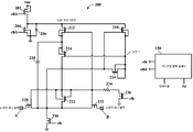
도 1을 참조하면, 본 발명의 구체적인 예시적인 실시예에 따른 고전압 부트스트랩 샘플링 회로의 개략도가 도시되어 있다. 일반적으로 숫자 100으로 표현되는 고전압 부트스트랩 샘플링 회로는 트랜지스터들(102, 104, 112, 114, 116, 118, 120, 122, 124, 126, 128, 130, 132, 136); 제너 다이오드(106), 커패시터(110), 및 저항기(108, 134)를 포함할 수 있다. 또한, 저전압 비중첩 제어 신호들(클록들), 예컨대 클록 출력들 "clk" 및 "clkb"를 생성하는 데 사용될 수 있는 비중첩 클럭 발생기(150)가 포함될 수 있다.Referring to Figure 1, a schematic diagram of a high voltage bootstrap sampling circuit in accordance with a specific exemplary embodiment of the present invention is shown. The high-voltage bootstrap sampling circuit, generally represented by the
제너 다이오드(106)는 엄격히 요구되지는 않지만, (스위치가 오프 상태로 전환될 때) 고전압 킥백(kickback)이 이러한 노드에 또한 접속되는 저전압 트랜지스터들을 손상시키는 것을 방지하기 위해 포함될 수 있다. 커패시터(110)는 약 1 피코패럿(pf) 내지 약 20 pf일 수 있으며, 트랜지스터들(120, 128, 132)(실제 스위치 트랜지스터들)의 게이트와 소스 사이에 인가되는 DC 전압을 유지하는 데 사용될 수 있다. 저항기(108)는 약 0 옴(미사용) 내지 약 100k 옴일 수 있고, 스위치의 오프-온 전환을 슬루-제한(slew-limit)하는 데 사용될 수 있다. 저항기(134)는 약 0 옴(미사용) 내지 약 100k 옴일 수 있고, 스위치의 온-오프 전환을 슬루-제한하는 데 사용될 수 있다. 고전압 멀티플렉서(100)는 어느 하나의 단자에서 0 내지 32 VDC 입력을 수용할 수 있고, 입력 전압과는 무관하게 0 내지 32 VDC 출력을 제공할 수 있다. 모든 제어 전압은, 예를 들어, 5 VDC, 3.3 VDC 또는 그 이하일 수 있지만 이로 제한되지 않는다. 고전압 부트스트랩 샘플링 회로(100)를 턴온시키기 위해, 스위치 트랜지스터들(120, 128, 132)의 게이트 및 소스는 clk를 로우(low)로 취함으로써 - 이는 트랜지스터(136)를 턴오프시킴 - GND로부터 분리된다. 부트스트랩 전압 입력(트랜지스터들(104, 102)에 의해 구동되는 전압)은 VBS(~5 VDC)로부터 GND로 스위칭된다. 이는 트랜지스터(114)가 턴온될 때까지 노드(1)를 풀다운한다. 트랜지스터(114)는 NMOS 스위치 트랜지스터들(120, 128, 132)의 Vgs에 걸쳐서 VBS, 예컨대 5 VDC를 가압하여, 이에 의해, 트랜지스터들(120, 128, 132)을 턴온시키고 그들을 전도성으로 만들며, 그에 의해 고전압 부트스트랩 샘플링 회로(100)가 턴온된다.
회로(고전압 부트스트랩 샘플링 회로(100)) 내의 모든 트랜지스터들은 항상 5 VDC 미만의 Vgs에서 유지된다(과도(transient) 전압을 포함함). PNP 트랜지스터들(122, 116)(이들은 또한 다이오드 또는 다이오드-접속형 MOSFET들일 수 있음)은 전환 동안 5 VDC를 초과할 수 있는 과도 전압을 억압하는 데에만 필수적이고, 모든 실시예들에서 필수적인 것은 아닐 수도 있다. 트랜지스터(120)에 결합된 것으로 도시된 제2 입력 경로는 고온에서 누설 오류를 감소시키기 위해 제공될 수 있다. 제2 입력 경로는 노드(A)와 동일한 전압, 또는 실질적으로 유사한 전압에 의해 구동될 것이다(예컨대, Vsense가 Vbus에 의해 구동될 수 있음).All the transistors in the circuit (high-voltage bootstrap sampling circuit 100) are always kept at Vgs less than 5 VDC (including the transient voltage). The
제너 다이오드(106)는 고전압 킥백에 대한 보호를 위한 것이고, 소정 응용예들에서는 요구되지 않을 수도 있다. 저항기들(108, 134)은 슬루-레이트 제한을 위한 것이고, 소정 응용예들의 경우에는 요구되지 않을 수도 있다. 바이폴라 접합 트랜지스터들(BJT)(116, 122, 124)은 "다이오드" 구성으로 접속된 금속 산화물 반도체 전계 효과 트랜지스터(MOSFET) 디바이스들로 대체될 수 있다. 트랜지스터들(102, 104)은 정상 저전압 MOSFET들일 수 있다. Vdd는 스위치를 턴온시키기 위해 고전압 게이트-소스 접합부에 걸쳐서 가압될 전압이다. 이는 HV MOSFET 기술에 따라 변할 수 있지만, 전형적으로 약 2 VDC 내지 약 5 VDC이다. 고전압 부트스트랩 샘플링 회로(100)가 오프인 경우, 출력 전압 노드는 다른 스위치 디바이스에 의해 하이 레벨로 구동될 수 있는데, 예컨대 이러한 스위치들 중 많은 것이 병렬로 접속될 수 있고 오프 스위치들은 스위칭-온된(switched-ON) 전압 출력에 의해 손상되지 않는다는 것이 중요하다.
고전압 부트스트랩 샘플링 회로(100)의 스위칭은 고전압 제어 신호들을 사용할 필요 없이 행해진다. 저전압 트랜지스터들(102, 104)을 포함하는 인버터 회로가 저전압 제어 신호에 의해 제어될 수 있다. 이러한 인버터가 VBS로부터 GND로 스위칭될 때, 트랜지스터(118)는 VDD로부터 GND를 향해 노드(1)를 풀다운하는데, 이는 트랜지스터(114)를 턴온시키기에 충분한 전압을 제공한다. 트랜지스터(114)가 통전되고 있기 때문에, 일차 스위치 트랜지스터들(120, 128, 132)은 인에이블되고 임의의 고전압 제어 로직이 필요 없이 (트랜지스터(114)를 통해 그들의 게이트 노드와 소스 노드 사이에 접속될 수 있는) 플로팅 커패시터(110)를 통해 이러한 트랜지스터들의 소스 노드를 계속해서 부스팅할 것이다. 트랜지스터(114)가 이 지점에서 그의 전도성 "온" 상태에 있다는 것을 상기한다.The switching of the high voltage
트랜지스터(들)(120)(및 선택적인 바이폴라 트랜지스터(122))를 포함하는 희생 입력 경로가 제공되어, 일차 입력 경로(트랜지스터들(128, 132))로부터의 누설 전류 및 스위칭 전류를 제거할 수 있다. 스위치를 통한 일차 경로(고전압 부트스트랩 샘플링 회로(100))는 2개의 백투백 HVNFET 디바이스들, 즉 트랜지스터들(128, 132)을 포함한다. 모든 전류가 일차 경로를 통해 흐르고 우회(divert)되지 않는 것이 바람직하다. 제2 입력 경로는, 명목상, 일차 경로의 복제로서, 트랜지스터(120)를 포함하고, 또한 유사한 HVNFET가, 트랜지스터들(120, 128, 132)과 연관된 게이트 커패시턴스, 및 커패시터(110)의 기생(하부 플레이트) 커패시턴스를 포함하는 스위칭 회로부 기생 부하뿐 아니라 다른 기생 부하(상호접속부 등)를 구동하는 데 필수적인 전류를 소싱하기 위해 사용될 수 있다. 이러한 제2 입력 경로는, 또한, 달리 일차 경로로부터 소싱할 필요가 있을 트랜지스터들(118, 124)을 통해 흐를 수 있는 디바이스 누설 전류의 대부분을 소싱한다.A sacrificial input path including transistor (s) 120 (and optional bipolar transistor 122) is provided to remove leakage current and switching current from the primary input path (
제2 입력은 트랜지스터(128)에 결합된 일차 입력의 것과 크기가 유사한 전압에 의해 구동될 수 있다. 이는 누설 전류 및 스위칭 전류 대 신호 전류에 대한 상이한 경로를 허용하여, 일차 입력으로부터의 전류 요건을 감소시키고 그것을 이차(프록시) 입력으로 시프트시킨다. 회로는 또한 이러한 특징부 없이 구성될 수 있는데, 이 경우에 그것은 도 2에 도시된 회로처럼 보인다. 또한 도 2에 도시된 바와 같이, 다이오드 접속형 BJT들은 고전압 PMOSFET 디바이스들로 대체되었다.The second input may be driven by a voltage similar in magnitude to that of the primary input coupled to the
도 1에 도시된 전체 회로의 변형예로서, 플로팅 커패시터(110)는 일차 입력 경로(트랜지스터들(128, 132)) 또는 이차 입력 경로(트랜지스터(120)) 중 어느 하나에 의해 교번하여 구동될 수 있다. 도 2에 도시된 실시예에서, 기생 커패시턴스는 선형성 및 설계 간소화를 위해 일차 경로에 의해 구동될 수 있다. 그러나, 제2 경로를 통해 그것을 구동하는 것은 일차 입력 상의 부하인가(loading)를 감소시킬 것이다.1, the floating
따라서, 도 1에 도시된 회로는, (1) 고전압 공급원 또는 (2) 고전압 제어 신호들을 요구하지 않고, 그리고 (3) 입력 신호로부터 상당한 전류를 소비하지 않고서, 고전압 신호들에 대한 전달 게이트 스위치로서 사용될 수 있다. 다이오드들 및 과보호 회로부가 제조 공정에 따라 실제 구현예에서 요구될 수 있거나 또는 요구되지 않을 수 있다는 것이 주목될 수 있다.Thus, the circuit shown in FIG. 1 can be implemented as (1) a high voltage supply or (2) without requiring high voltage control signals and (3) as a transfer gate switch for high voltage signals without consuming significant current from the input signal Can be used. It is noted that diodes and overprotect circuitry may or may not be required in actual implementations depending on the fabrication process.
도 2를 참조하면, 본 발명의 다른 구체적인 예시적인 실시예에 따른 고전압 부트스트랩 샘플링 회로의 개략도가 도시되어 있다. 도 2에 도시된 회로는 도 1에 도시되고 위에서 설명된 회로와 실질적으로 동일한 방식으로 동작한다.Referring to Figure 2, a schematic diagram of a high voltage bootstrap sampling circuit in accordance with another specific exemplary embodiment of the present invention is shown. The circuit shown in Fig. 2 operates in substantially the same manner as the circuit shown in Fig. 1 and described above.
위에서 개시된 다양한 실시예들은 데이터시트 내의 핵심적인 차별점을 가능하게 한다: 작은 스위칭된 커패시터 전류가 ~ 나노암페어 범위에 있기 때문에 입력으로부터 0의 전류를 소비한다. (하기의 회로의 ESD 누설 및 스위칭된 커패시터 전류가 이를 대략 ~1 ㎂로 증가시킬 수 있음). 입력의 관점에서, 이러한 디바이스는 수동 디바이스로 보일 수 있으며, 이에 의해, 상이한 입력 경로들 사이의 이상적인 매칭이 설계에 의해 보장되고 4x 멀티플렉싱된 입력 경로들 사이의 측정된 ~< 1 LSB (16 비트) 매칭이 제공될 수 있다. 다양한 실시예에 따른 이러한 고전압 멀티플렉서(100)는 복제 DC-오프셋 교정 및 오프셋 디더링을 허용하며, 이에 의해, 측정된 < 1 LSB (3 ㎶) 입력 오프셋 전압이 전체 시스템(32 VDC 범위)을 통해 제공된다. 다양한 실시예들은, 추가로, 측정을 손상시키지 않고서, 입력들의 외부 저항기-커패시터(RC) 필터링을 허용한다. 종래의 디바이스들은 인쇄 회로 기판(PCB) 트레이스 저항 및 외부 저항기들이 측정에 오류를 일으키는 것을 경고를 한다. 예를 들어, 일부 종래의 디바이스들은 하기를 명시한다: "감지 저항기들을 가능한 한 디바이스에 가깝게 배치하고 최소 폭 PCB 트레이스들을 사용하지 않는 것이 추천된다". 다양한 실시예들에 따른, 프론트엔드 디바이스를 포함하는 평가 보드가 각각의 입력 상에 100 옴 직렬 저항기들을 포함할 수 있다(요구되지 않음). 이는 시스템 사용자가 감지 저항기들을 그들이 최상의 감지를 행하는 생성 회로부에 가깝게 배치하게 한다.The various embodiments disclosed above enable a key differentiator within the data sheet: a small switched capacitor current consumes zero current from the input because it is in the ~ nanoamp range. (ESD leakage in the circuit below and the switched capacitor current may increase it to approximately ~ 1 μA). From an input perspective, such a device can be viewed as a passive device, whereby an ideal match between different input paths is guaranteed by design and a measured ~ 1 LSB (16 bits) between 4x multiplexed input paths, Matching can be provided. This
도 3을 참조하면 2개의 고전압 스위치들을 포함하는 단일 채널 차동 입력 멀티플렉서를 갖는 샘플링 회로의 개략도가 도시되어 있다. 본 발명의 교시내용에 따르면, 작은 차동 전압이 큰 공통 모드 전압의 상단에서 측정되어야 한다. 공통 모드는 약 0 VDC 내지 약 32 VDC일 수 있다. 차동 신호는 예를 들어 +/-25 ㎷ 만큼 작을 수 있는데, 예를 들어 감지 저항기를 통하는 전류에 의해 야기되는 전압일 수 있다. 이러한 회로에 대한 공급 전압은 예를 들어 2.6 VDC일 수 있지만 이로 제한되지 않는다. 제한이 아닌 일례로서, 8개의 입력이 멀티플렉싱될 수 있는데, 이때 각각의 입력은 상이한(미지의) 공통 모드 전압 VCM을 갖는다. 도 3에 도시된 회로는 (고 VCM에서) 작은 차동 전압을 측정하고 그것을 더 큰 저전압 신호로 변환하기 위해 상위-레벨 시스템에서 사용될 수 있는 스위치-멀티플렉서의 일례이다.Referring to FIG. 3, there is shown a schematic diagram of a sampling circuit having a single-channel differential input multiplexer including two high-voltage switches. According to the teachings of the present invention, a small differential voltage must be measured at the top of the large common mode voltage. The common mode may be between about 0 VDC and about 32 VDC. The differential signal may be as small as, for example, +/- 25 ㎷, for example a voltage caused by a current through a sense resistor. The supply voltage for this circuit may be, for example, 2.6 VDC, but is not limited thereto. By way of example, and not by way of limitation, eight inputs may be multiplexed, with each input having a different (unknown) common mode voltage V CM . The circuit shown in FIG. 3 is an example of a switch-multiplexer that can be used in a high-level system to measure a small differential voltage (at high VCM) and convert it to a larger, low voltage signal.
도 4를 참조하면, 종래 기술의 샘플링 회로들의 개략적인 블록도들이 도시되어 있다. 도 4에 도시된 종래 기술의 샘플링 회로들은 고전압측 레일이 사용가능하지 않으므로, 입력 신호 자체로부터 전력이 취해진다. 측정되고 있는 입력으로부터 취해진 전력은 핵심 파라미터이다. 예를 들어, 본 출원의 양수인에 의해 제조된 PAC1921은 멀티플렉서들을 사용하지 않고, 각각의 입력 채널로부터 약 35 마이크로암페어를 취한다. 본 출원의 양수인에 의해 제조된 PAC1720(도시되지 않음)은 2-채널 멀티플렉서를 포함하고, 각각의 입력 채널로부터 약 150 마이크로암페어를 취한다. 본 명세서에 개시된 다양한 실시예들에 따르면, 설계 목표는 4-채널 멀티플렉서의 경우에 약 1 마이크로암페어 미만일 수 있다. 종래 기술에 비해 상당한 개선. 이러한 경우에, PAC1921은 저항기 디바이더를 사용하여 VBUS 전압(0 내지 32 v)을 0 내지 3 v의 전압으로 나눔으로써 그를 측정한다. PAC1921은, VBUS와 VSENSE 사이의 작은 차동 전압을 버퍼링하고 생성된 신호를 저전압 ADC로 구동하기 위해 VBUS 전력 공급원 상에서 동작하는 차동 증폭기를 사용한다. 도 4에 도시된 블록도로부터의 MAX34407은 또한 외부 VBUS 전력 공급원으로부터 동작하는 능동 고전압 버퍼를 포함한다.Referring to Figure 4, schematic block diagrams of prior art sampling circuits are shown. The prior art sampling circuits shown in Figure 4 are powered from the input signal itself, since high voltage side rails are not available. The power taken from the input being measured is a key parameter. For example, the PAC1921 made by the Assignee of the present application does not use multiplexers and takes about 35 microamps from each input channel. A PAC 1720 (not shown) manufactured by the assignee of the present application includes a two-channel multiplexer and takes about 150 microamps from each input channel. According to various embodiments disclosed herein, the design goals may be less than about one microampere for a four-channel multiplexer. Significant improvement over the prior art. In this case, the PAC1921 measures it by dividing the VBUS voltage (0 to 32 V) by a voltage of 0 to 3 V using a resistor divider. The PAC1921 uses a differential amplifier that operates on the VBUS power supply to buffer a small differential voltage between VBUS and VSENSE and drive the generated signal to a low-voltage ADC. The MAX34407 from the block diagram shown in Figure 4 also includes an active high voltage buffer operating from an external VBUS power supply.
도 4에 도시된 것들과 같은 본 기술의 디바이스들은: a) 하이-측 입력으로부터 전력공급받는 차동 입력 버퍼 증폭기를 포함한다(가장 일반적임). 본 기술의 증폭기들은 측정되고 있는 전압 입력으로부터의 DC 전류를 사용하고 0 VDC에 이르기까지 작동하지 않는다. 채널-채널 미스매칭의 소스가 이러한 본 기술의 디바이스들에 존재한다. 어느 차동 입력이 최고 전압을 전달하는지가 알려져 있지 않기 때문에 양방향 입력을 만드는 것은 어렵고; b) 일부 본 기술의 디바이스들에서, 스위치 트랜지스터는 그러한 본 기술 디바이스들에서 하이-측 입력으로부터 전력공급받고, 그들은 입력으로부터의 DC 전류를 사용하여 스위치에 대한 Vgs를 생성한다. 또한, 이것은 0 VDC에 이르기까지 작동하지 않고, 그 자체를 멀티플렉싱 구성에 제공하지 않으며; c) 일부 본 기술의 디바이스들은 AC-결합된 스위칭 제어를 이용하는데, 이는 높은 가변성을 야기하고 그 자체를 멀티플렉싱 구성에 제공하지도 않고, 또한 턴오프되기 어려우며(DC 누설이 높을 수 있음); 그리고 d) 일부 본 기술의 디바이스들은 입력에서 저항기 디바이더를 사용하는데, 이는 입력으로부터의 DC 전류를 사용하고, 채널-채널 매칭을 약 8 비트로 제한하고, 신호 대 잡음비(SNR)를 손상시킨다.Devices of the present technology, such as those shown in Figure 4, include: a) a differential input buffer amplifier powered from the high-side input (most common). The amplifiers in this technology use DC current from the voltage input being measured and do not operate down to 0 VDC. The source of the channel-channel mismatch exists in the devices of this technology. It is difficult to make a bidirectional input because it is not known which differential input carries the highest voltage; b) In some devices of the present technology, the switch transistors are powered from the high-side input in such technology devices, which use the DC current from the input to generate Vgs for the switch. Also, it does not operate up to 0 VDC and does not provide itself to the multiplexing configuration; c) Some devices of the present technology use AC-coupled switching control, which causes high variability and does not provide itself in multiplexing configurations, is also difficult to turn off (DC leakage can be high); And d) some devices of the present technology use a resistor divider at the input, which uses DC current from the input, limits the channel-channel matching to about 8 bits, and degrades the signal-to-noise ratio (SNR).
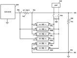
도 5를 참조하면, 본 발명의 교시내용에 따른, 도 1 및 도 2에 도시되고 샘플링 회로 아날로그-디지털 변환기(ADC)에 전력 공급원의 전류 및 전압 측정치들을 결합시키도록 구성된 고전압 부트스트랩 샘플링 회로들의 간략화된 예시적인 응용예의 개략적인 블록도가 도시되어 있다. 복수의 고전압 부트스트랩 샘플링 회로들(100/200)은 전류 감지 저항기(542)에 결합될 수 있고, 전력 공급원 출력 전압은 부하(저항기)(550)에 걸쳐서 측정될 수 있다. 복수의 고전압 부트스트랩 샘플링 회로들(100/200) 중 선택된 하나가 상이한 전압 노드들(552, 554, 556)을 샘플앤드홀드 커패시터(548)에 접속시킬 수 있다. 복수의 고전압 부트스트랩 샘플링 회로들(100/200) 중 2개가 측정될 전압 노드들의 플러스 및 마이너스 전압들을 샘플앤드홀드 커패시터(548)에 결합시키도록 선택될 수 있다. 이어서, 이들 2개의 부트스트랩 샘플링 회로들(100/200)은 턴오프되고(샘플핸드홀드 커패시터(548)로부터 분리됨), 샘플 스위치(546)는 폐쇄된다. 이에 의해, 샘플앤드홀드 커패시터(548) 상에 저장된 샘플링된 전압은 아날로그-디지털 변환기(ADC)(544)의 차동 입력(+/-)에 결합되고, 아날로그-디지털 변환기(ADC)(544)는 이어서 저장된 샘플링된 전압을 그의 프로세싱을 위해 마이크로제어기(도시되지 않음)에 결합될 수 있는 디지털 값으로 변환할 수 있다.Referring to FIG. 5, high-voltage bootstrap sampling circuits, shown in FIGS. 1 and 2 and configured to combine the current and voltage measurements of a power source with a sampling circuit analog-to-digital converter (ADC), according to the teachings of the present invention A schematic block diagram of a simplified exemplary application is shown. A plurality of high voltage
예를 들어,E.g,
노드(552)는 고전압 샘플 회로(100b)가 인에이블될 때 (+) 커패시터(548)에 결합된다.
노드(554)는 고전압 샘플 회로(100a)가 인에이블될 때 (-) 커패시터(548)에 결합된다.Node 554 is coupled to (-)
노드(552)는 고전압 샘플 회로(100d)가 인에이블될 때 (-) 커패시터(548)에 결합된다.
노드(554)는 고전압 샘플 회로(100c)가 인에이블될 때 (+) 커패시터(548)에 결합된다.Node 554 is coupled to (+)
노드(556)는 고전압 샘플 회로(100e)가 인에이블될 때 (-) 커패시터(548)에 결합된다.
노드(556)는 고전압 샘플 회로(100f)가 인에이블될 때 (+) 커패시터(548)에 결합된다.
따라서, 저항기(542)에 걸친 전압 강하(부하로 공급되는 전력 공급원 전류)는 포지티브 전압(고전압 샘플 회로들(100b, 100a)이 인에이블됨) 또는 네거티브 전압(고전압 샘플 회로들(100d, 100c)이 인에이블됨) 중 어느 하나로서 측정될 수 있다. 부하(저항기(550))에 공급되는 전압은 포지티브 전압(고전압 샘플 회로들(100c, 100e)이 인에이블됨) 또는 네거티브 전압(고전압 샘플 회로들(100a, 100f)이 인에이블됨) 중 어느 하나로서 측정될 수 있다. 포지티브 및 네거티브 전압 측정과 평균화 사이에서 교번함으로써, 보다 정확한 전압 측정이 얻어질 수 있다.Thus, the voltage drop across the resistor 542 (the power source current supplied to the load) is reduced to a positive voltage (high
양방향 측정 능력, 예컨대 플러스(+) 또는 마이너스(-) 차동 전압 측정이 또한 바람직한 핵심 파라미터로 간주될 수 있다. 종래 기술의 측정 회로들은 전력 소비 또는 복잡도에 있어서 상당한 페널티가 없이 양방향 측정을 용이하게 지원하지 않는다. 그것은 어느 레일이 더 높은 전압 전위를 전달할 수 있는지를 모르기 때문에 어려우며, 종래 기술은 동작 전력을 위해 더 높은(더 포지티브인) 전압 전위에 의존할 수 있다.Bidirectional measurement capability, such as positive (+) or negative (-) differential voltage measurement, may also be regarded as a desirable core parameter. Prior art measurement circuits do not readily support bi-directional measurements without significant penalty in power consumption or complexity. It is difficult because it does not know which rails can carry higher voltage potentials, and the prior art can rely on a higher (more positive) voltage potential for operating power.
본 발명의 교시내용에 따른, 그리고 도 3에 도시된, 멀티플렉서를 구현하는 다른 방법은, 먼저 노드(370)에서 (스위치(374)를 통해) 하나의 전압(VBUS)을 샘플링하고 이를 커패시터(378) 상에 저장하는 한편, 다른 커패시터(382)는 스위치(380)를 통해 0 볼트로 리셋되는 것이다. 이어서, 노드(372) 상의 다른 전압(VSENSE)을 (스위치(376)를 통해) 커패시터(378) 상으로 스위칭하여, 연산 증폭기(384)가 N:1 커패시턴스 비, 예를 들어 8:1 커패시턴스 비 - 그러나, 특정 커패시턴스 비로 제한되지 않음 - 를 통해 커패시터(382) 상으로 그 차이를 확대하게 할 것이다.Another method of implementing the multiplexer, according to the teachings of the present invention and shown in FIG. 3, is to first sample one voltage (VBUS) at node 370 (via switch 374) While the
위에서 개시된 다양한 실시예들은 제품 성능에서의 핵심적인 차별점을 가능하게 한다: 작은 스위칭된 커패시터 전류가 ~ 나노암페어 범위에 있기 때문에, 입력 전압으로부터 실질적으로 어떠한 전류도 소비하지 않는다. (하기의 회로의 ESD 누설 및 스위칭된 커패시터 전류가 이를 ~1 ㎂로 증가시킬 수 있음). 입력의 관점에서, 이러한 디바이스는 수동 디바이스로 보일 수 있으며, 이에 의해, 상이한 입력 경로들 사이의 이상적인 매칭이 설계에 의해 보장되고 4x 멀티플렉싱된 입력 경로들 사이의 측정된 ~1 LSB (16b) 매칭이 제공될 수 있다. 다양한 실시예에 따른 이러한 고전압 멀티플렉서(100)는 복제 DC-오프셋 교정 및 오프셋 디더링을 허용하며, 여기서 측정된 < 1 LSB (3 ㎶) 입력 오프셋 전압이 전체 시스템(32 VDC 범위)을 통해 제공된다. 다양한 실시예들은, 추가로, 측정을 손상시키지 않고서, 입력들의 외부 저항기-커패시터(RC) 필터링을 허용한다. 종래의 디바이스들은 인쇄 회로 기판(PCB) 트레이스 저항 및 외부 저항기들이 측정에 오류를 일으키는 것을 경고를 한다. 예를 들어, 일부 종래의 디바이스 사양은 하기를 명시한다: "감지 저항기들을 가능한 한 디바이스에 가깝게 배치하고 최소 폭 PCB 트레이스들을 사용하지 않는 것이 추천된다". 다양한 실시예들에 따른, 프론트엔드 디바이스를 포함하는 평가 보드가 각각의 입력 상에 100 옴 직렬 저항기들을 포함할 수 있다(요구되지 않음). 이는 시스템 사용자가 감지 저항기들을 그들이 최상의 감지를 행하는 생성 회로부에 가깝게 배치하게 한다.The various embodiments described above enable a key differentiator in product performance: they do not consume substantially any current from the input voltage because the small switched capacitor current is in the ~ nanoamp range. (ESD leakage and switched capacitor current in the circuit below may increase this to ~ 1 μA). From an input perspective, such a device can be viewed as a passive device, whereby an ideal match between different input paths is guaranteed by design and a measured ~ 1 LSB (16b) match between 4x multiplexed input paths Can be provided. This
종래의 부품들은 고전압 입력으로부터 약 10 ㎂ 내지 약 100 ㎂를 소비한다. 다양한 실시예들은 입력들로부터의 나노암페어 레벨 바이어스 전류를 허용한다. 이러한 낮은 바이어스 전류는 "감지 저항기들"이 고전압 멀티플렉서(100)로부터 멀리 위치되게 하고 또한 RC 저역 필터링이 입력 핀들에서 사용되게 한다. 이러한 설계는 또한 상당한 측정 회로 오류가 보이기 전에 킬로옴 저항을 허용한다.Conventional components consume about 10 [mu] A to about 100 [mu] A from a high voltage input. Various embodiments allow a nanoamperes bias current from the inputs. This low bias current causes the " sense resistors " to be located away from the
Claims (18)
적어도 하나의 저전압 제어 신호에 결합되는 저전압 인버터를 제공하는 단계;
상기 저전압 인버터에 결합되고 그에 의해 제어되는 제1 고전압 트랜지스터를 제공하는 단계;
상기 제1 고전압 트랜지스터에 결합되고 그에 의해 제어되는 제2 고전압 트랜지스터를 제공하는 단계; 및
상기 제2 고전압 트랜지스터에 결합되고 그에 의해 제어되는 제3 및 제4 고전압 트랜지스터들을 백투백으로(back-to-back) 포함하는 일차 입력/출력 신호 경로를 제공하는 단계를 포함하고,
상기 저전압 인버터는 상기 제1 고전압 트랜지스터를 턴온시키고,
상기 제1 고전압 트랜지스터는 상기 제2 고전압 트랜지스터를 턴온시키고,
상기 제2 고전압 트랜지스터는 상기 제3 및 상기 제4 고전압 트랜지스터들을 턴온시킴으로써 상기 일차 입력/출력 신호 경로를 인에이블시키는, 방법.A method for controlling a high voltage switching circuit with low voltage control signals,
Providing a low voltage inverter coupled to at least one low voltage control signal;
Providing a first high voltage transistor coupled to and controlled by the low voltage inverter;
Providing a second high voltage transistor coupled to and controlled by the first high voltage transistor; And
Providing a primary input / output signal path comprising back-to-back third and fourth high voltage transistors coupled to and controlled by the second high voltage transistor,
The low-voltage inverter turns on the first high-voltage transistor,
The first high voltage transistor turns on the second high voltage transistor,
And the second high voltage transistor enables the primary input / output signal path by turning on the third and fourth high voltage transistors.
저전압 제어 신호들만을 사용하여 플로팅 커패시터와 함께 상기 제2 고전압 트랜지스터의 소스를 부스팅하는 단계를 추가로 포함하는, 방법.The method according to claim 1,
Further comprising boosting the source of the second high voltage transistor with the floating capacitor using only the low voltage control signals.
상기 일차 입력/출력 신호 경로로부터의 누설 전류 및 스위칭 전류를 제거하기 위해 이차 경로를 제공하는 단계를 추가로 포함하는, 방법.3. The method of claim 2,
Further comprising providing a secondary path to eliminate leakage current and switching current from the primary input / output signal path.
상기 이차 경로로부터 상기 고전압 트랜지스터들을 구동하는 데 필요한 제어 전류를 제공하는 단계를 추가로 포함하는, 방법.7. The method according to any one of claims 3 and 5,
Further comprising providing a control current necessary to drive the high voltage transistors from the secondary path.
상기 이차 경로로부터 상기 고전압 트랜지스터들에 대한 누설 전류를 제공하는 단계를 추가로 포함하는, 방법.The method according to any one of claims 3, 4, and 6,
And providing a leakage current for the high voltage transistors from the secondary path.
상기 일차 경로 또는 상기 이차 경로 중 어느 하나로부터 상기 플로팅 커패시터를 구동하는 단계를 추가로 포함하는, 방법.6. The method according to any one of claims 3 to 5,
Further comprising driving the floating capacitor from either the primary path or the secondary path.
상기 고전압 스위칭 회로는 고전압 공급원 또는 고전압 제어 신호들을 요구하지 않으면서 고전압 신호들에 대한 전달 게이트 스위치로서 사용되는, 방법.The method according to any one of claims 1 to 6 or 8,
Wherein the high voltage switching circuit is used as a transfer gate switch for high voltage signals without requiring a high voltage supply or high voltage control signals.
상기 고전압 스위칭 회로는 고전압 입력 신호로부터 상당한 전류를 소비하지 않으면서 고전압 신호들에 대한 전달 게이트 스위치로서 사용되는, 방법.8. The method according to any one of claims 1 to 7,
Wherein the high voltage switching circuit is used as a transfer gate switch for high voltage signals without consuming significant current from the high voltage input signal.
고전압 공급원, 고전압 제어 신호들을 요구하지 않고서 고전압 신호에 결합하기 위한 전달 게이트 스위치로서 구성되고, 상기 고전압 신호로부터 전류를 인출하지 않는, 고전압 스위칭 회로.15. The method according to any one of claims 9 to 14,
A high voltage switching circuit configured as a high voltage supply, a transfer gate switch for coupling to a high voltage signal without requiring high voltage control signals, and not drawing current from the high voltage signal.
일차 전류 경로를 추가로 포함하고, 모든 전류가 상기 일차 전류 경로를 통해 흐르는, 고전압 스위칭 회로.11. The method according to claim 9 or 10,
Further comprising a primary current path, wherein all current flows through the primary current path.
상기 일차 전류 경로의 고전압 입력 및 출력 트랜지스터들을 구동하는 데 필요한 전류를 소싱(source)하기 위해 사용되는 제2 입력 전류 경로를 추가로 포함하는, 고전압 스위칭 회로.12. The method of claim 11,
Further comprising a second input current path that is used to source the high voltage inputs of the primary current path and the current needed to drive the output transistors.
상기 제2 입력 전류 경로는 상기 일차 전류 경로에 의해 소싱되었을 실질적으로 모든 누설 전류를 소싱하는, 고전압 스위칭 회로.15. The method according to claim 12 or 14,
The second input current path sourcing substantially all of the leakage current that would have been sourced by the primary current path.
상기 일차 또는 제2 입력 전류 경로 중 어느 하나에 의해 구동되는 플로팅 커패시터를 추가로 포함하는, 고전압 스위칭 회로.The method according to claim 12 or 13,
Further comprising a floating capacitor driven by either the primary or the second input current path.
공통 접속부를 갖는 제1 및 제2 샘플 스위치들 - 또한,
상기 제1 샘플 스위치는 VBUS 노드에 결합되고,
상기 제2 샘플 스위치는 VSENSE 노드에 결합됨 -;
상기 공통 접속부에 결합되는 하나의 노드를 갖는 제1 샘플 커패시터;
상기 제1 샘플 커패시터의 다른 노드에 결합되는 하나의 노드를 갖는 제2 샘플 커패시터;
상기 제2 샘플 커패시터와 병렬로 결합된 단락 스위치; 및
상기 제1 샘플 커패시터와 상기 제2 샘플 커패시터 사이의 접합부에 결합되는 입력 및 상기 제2 샘플 커패시터의 다른 노드에 결합되는 출력을 갖는 연산 증폭기를 포함하고,
상기 제1 및 제2 샘플러 스위치들은 저전압 제어 신호들에 의해 제어되는 고전압 입력 및 출력 트랜지스터들을 포함하는, 샘플링 회로 및 멀티플렉서.A sampling circuit and a multiplexer,
First and second sample switches having a common connection,
The first sample switch is coupled to a VBUS node,
The second sample switch coupled to a VSENSE node;
A first sample capacitor having one node coupled to the common connection;
A second sample capacitor having one node coupled to another node of the first sample capacitor;
A shorting switch coupled in parallel with the second sample capacitor; And
An operational amplifier having an input coupled to a junction between the first sample capacitor and the second sample capacitor and an output coupled to another node of the second sample capacitor,
Wherein the first and second sampler switches comprise high voltage input and output transistors controlled by low voltage control signals.
상기 2-극 스위치에 결합되는 차동 입력을 갖는 아날로그-디지털 변환기(ADC)를 추가로 포함하는, 샘플링 회로 및 멀티플렉서.18. The method according to claim 15 or 17,
Further comprising an analog-to-digital converter (ADC) having a differential input coupled to the two-pole switch.
전력 공급원과 부하 사이에 결합하도록 구성된 감지 저항기를 추가로 포함하고,
상기 복수의 고전압 스위칭 회로들의 고전압 입력들 중 일부 고전압 입력들은 상기 감지 저항기의 전력 공급원 측에 결합되고;
상기 복수의 고전압 스위칭 회로들의 고전압 입력들 중 일부 다른 고전압 입력들은 상기 감지 저항기의 부하 측에 결합되는, 샘플링 회로 및 멀티플렉서.17. The method according to claim 15 or 16,
Further comprising a sense resistor configured to couple between the power source and the load,
Wherein some of the high voltage inputs of the plurality of high voltage switching circuits are coupled to the power supply side of the sense resistor;
And some other high voltage inputs of the high voltage inputs of the plurality of high voltage switching circuits are coupled to the load side of the sense resistor.
고전압 입력들 및 고전압 출력들, 및 저전압 제어 입력들을 포함하는 복수의 고전압 스위칭 회로들;
상기 고전압 출력들 중 일부 고전압 출력들에 결합되는 제1 노드 및 상기 고전압 출력들 중 일부 다른 고전압 출력들에 결합되는 제2 노드를 갖는 샘플앤드홀드(sample and hold) 커패시터; 및
상기 제1 노드에 결합되는 하나의 극(pole) 및 상기 제2 노드에 결합되는 다른 극을 갖는 2-극 스위치를 포함하는, 샘플링 회로 및 멀티플렉서.A sampling circuit and a multiplexer,
A plurality of high voltage switching circuits including high voltage inputs and high voltage outputs, and low voltage control inputs;
A sample and hold capacitor having a first node coupled to some of the high voltage outputs of the high voltage outputs and a second node coupled to some of the other high voltage outputs of the high voltage outputs; And
And a two-pole switch having one pole coupled to the first node and another pole coupled to the second node.
Applications Claiming Priority (5)
| Application Number | Priority Date | Filing Date | Title |
|---|---|---|---|
| US201662406881P | 2016-10-11 | 2016-10-11 | |
| US62/406,881 | 2016-10-11 | ||
| US15/729,294 US10163521B2 (en) | 2016-10-11 | 2017-10-10 | High voltage bootstrap sampling circuit |
| US15/729,294 | 2017-10-10 | ||
| PCT/US2017/056050 WO2018071479A1 (en) | 2016-10-11 | 2017-10-11 | High voltage bootstrap sampling circuit |
Publications (1)
| Publication Number | Publication Date |
|---|---|
| KR20190060755A true KR20190060755A (en) | 2019-06-03 |
Family
ID=61829094
Family Applications (1)
| Application Number | Title | Priority Date | Filing Date |
|---|---|---|---|
| KR1020197003959A KR20190060755A (en) | 2016-10-11 | 2017-10-11 | High-Voltage Bootstrap Sampling Circuit |
Country Status (7)
| Country | Link |
|---|---|
| US (1) | US10163521B2 (en) |
| EP (1) | EP3526898A1 (en) |
| JP (1) | JP7061110B2 (en) |
| KR (1) | KR20190060755A (en) |
| CN (1) | CN109643992B (en) |
| TW (1) | TW201826711A (en) |
| WO (1) | WO2018071479A1 (en) |
Cited By (1)
| Publication number | Priority date | Publication date | Assignee | Title |
|---|---|---|---|---|
| KR102435395B1 (en) * | 2021-02-25 | 2022-08-22 | 한국항공대학교산학협력단 | Sampling switch for high dynamic input range and method for operating the same |
Families Citing this family (7)
| Publication number | Priority date | Publication date | Assignee | Title |
|---|---|---|---|---|
| US10163521B2 (en) * | 2016-10-11 | 2018-12-25 | Microchip Technology Incorporated | High voltage bootstrap sampling circuit |
| US10686458B1 (en) * | 2017-08-01 | 2020-06-16 | Liming Xiu | Method and apparatus for improving frequency source frequency accuracy and frequency stability |
| US11699993B2 (en) * | 2020-09-15 | 2023-07-11 | Micron Technology, Inc. | Signal sampling with offset calibration |
| CN112636759A (en) * | 2020-12-31 | 2021-04-09 | 成都思瑞浦微电子科技有限公司 | Sampling circuit |
| US20240048108A1 (en) * | 2022-08-05 | 2024-02-08 | Cirrus Logic International Semiconductor Ltd. | Beyond-the-rails bootstrapped sampling switch |
| CN115425958B (en) * | 2022-11-04 | 2023-02-17 | 西安水木芯邦半导体设计有限公司 | Gate-source voltage holding circuit for controlling high-voltage analog switch |
| CN116961655B (en) * | 2023-09-21 | 2023-12-08 | 电子科技大学 | Chopper sampling circuit applied to high-precision ADC |
Family Cites Families (37)
| Publication number | Priority date | Publication date | Assignee | Title |
|---|---|---|---|---|
| US5603726A (en) * | 1989-09-22 | 1997-02-18 | Alfred E. Mann Foundation For Scientific Research | Multichannel cochlear implant system including wearable speech processor |
| US5531774A (en) * | 1989-09-22 | 1996-07-02 | Alfred E. Mann Foundation For Scientific Research | Multichannel implantable cochlear stimulator having programmable bipolar, monopolar or multipolar electrode configurations |
| US5938691A (en) * | 1989-09-22 | 1999-08-17 | Alfred E. Mann Foundation | Multichannel implantable cochlear stimulator |
| JPH05286150A (en) * | 1992-03-05 | 1993-11-02 | Internatl Business Mach Corp <Ibm> | Monitor circuit and control circuit of print hammer coil current |
| US5572155A (en) * | 1994-06-20 | 1996-11-05 | Fuji Photo Film Co., Ltd. | CCD signal read-out circuit free from ailiasing of high-frequency noises |
| EP0729232B1 (en) * | 1995-02-22 | 2003-09-17 | Texas Instruments Incorporated | A high voltage analog switch |
| US5839959A (en) * | 1996-03-26 | 1998-11-24 | Pacific Digital Peripherals, Inc. | Joystick game adapter card for a personal computer |
| US6078311A (en) * | 1996-03-26 | 2000-06-20 | Pacific Digital Peripherals, Inc. | Joystick game adapter card for a personal computer |
| US6017273A (en) * | 1996-03-26 | 2000-01-25 | Pacific Digital Peripherals, Inc. | Joystick game adapter card for a personal computer |
| US6208542B1 (en) * | 1998-06-30 | 2001-03-27 | Sandisk Corporation | Techniques for storing digital data in an analog or multilevel memory |
| US6326740B1 (en) * | 1998-12-22 | 2001-12-04 | Philips Electronics North America Corporation | High frequency electronic ballast for multiple lamp independent operation |
| US6738275B1 (en) * | 1999-11-10 | 2004-05-18 | Electromed Internationale Ltee. | High-voltage x-ray generator |
| US8571179B2 (en) * | 1999-11-10 | 2013-10-29 | Robert Beland | Computed tomography systems |
| FR2818423B1 (en) * | 2000-12-20 | 2003-04-04 | Chauvin Arnoux | METHOD FOR ACQUISITION BY SAMPLING ANALOG SIGNALS AND ACQUISITION SYSTEM FOR IMPLEMENTING THIS METHOD |
| KR100520682B1 (en) | 2004-02-25 | 2005-10-11 | 주식회사 하이닉스반도체 | High voltage switch circuit for semiconductor device |
| US7176742B2 (en) | 2005-03-08 | 2007-02-13 | Texas Instruments Incorporated | Bootstrapped switch with an input dynamic range greater than supply voltage |
| US7479811B2 (en) * | 2005-09-08 | 2009-01-20 | Mediatek Inc. | Sample/hold circuit module |
| EP2128633B1 (en) | 2008-05-29 | 2012-05-02 | Austriamicrosystems AG | Current-sense amplifier arrangement and method for measuring a voltage signal |
| EP2173031B1 (en) | 2008-10-01 | 2012-06-06 | Austriamicrosystems AG | Amplifier arrangement, measurement arrangement and signal processing method |
| US7816951B1 (en) * | 2008-10-10 | 2010-10-19 | National Semiconductor Corporation | Locally boosted top plate sampling for a sampling capacitor |
| US8502594B2 (en) | 2008-12-31 | 2013-08-06 | Linear Technology Corporation | Bootstrap transistor circuit |
| US7952419B1 (en) | 2009-11-16 | 2011-05-31 | Analog Devices, Inc. | Bootstrapped switch circuit |
| CN102098034B (en) * | 2009-12-15 | 2014-07-30 | 北京中星微电子有限公司 | Bootstrap sampling circuit |
| EP2506685A4 (en) * | 2010-12-02 | 2013-10-16 | Sunsun Lighting China Co Ltd | Led driving power supply circuit, driving power supply and lighting device |
| WO2012077125A1 (en) * | 2010-12-08 | 2012-06-14 | Deepak Chandran | A system for monitoring and controlling high intensity discharge (hid) lamps |
| US8299837B1 (en) * | 2011-08-16 | 2012-10-30 | Himax Technologies Limited | Integrator-based common mode stabilization method applied to pseudo-differential switched-capacitor circuit |
| KR20130072804A (en) * | 2011-12-22 | 2013-07-02 | 에스케이하이닉스 주식회사 | Circuit for sampling signal and image sensor including the same |
| US8810301B1 (en) * | 2012-06-22 | 2014-08-19 | Cadence Design Systems, Inc. | System and method for level shifting signals with adjustably controlled frequency response |
| JP6154705B2 (en) * | 2013-09-24 | 2017-06-28 | 株式会社 日立パワーデバイス | Semiconductor switch circuit, signal processing apparatus, and ultrasonic diagnostic apparatus |
| US9178413B2 (en) * | 2013-11-19 | 2015-11-03 | Active-Semi, Inc. | Power factor correction autodetect |
| US9287862B2 (en) * | 2013-12-26 | 2016-03-15 | Texas Instruments Incorporated | Bootstrapped sampling switch circuits and systems |
| US10439491B2 (en) * | 2014-02-14 | 2019-10-08 | Telefonaktiebolaget Lm Ericsson (Publ) | Power supply electronic circuit with IBC to control current ripple |
| US9576679B2 (en) * | 2014-10-09 | 2017-02-21 | Silicon Laboratories Inc. | Multi-stage sample and hold circuit |
| US10148174B2 (en) * | 2016-03-28 | 2018-12-04 | Qualcomm Incorporated | Duty cycle estimator for a switch mode power supply |
| US9906143B1 (en) * | 2016-09-30 | 2018-02-27 | Dell Products L.P. | Systems and methods for diagnostic current shunt and overcurrent protection (OCP) for power supplies |
| US10163521B2 (en) * | 2016-10-11 | 2018-12-25 | Microchip Technology Incorporated | High voltage bootstrap sampling circuit |
| US10034336B1 (en) * | 2017-09-22 | 2018-07-24 | Dialog Semiconductor (Uk) Limited | Controlling output voltage to achieve ultra-low standby power in dim-to-off LED applications |
-
2017
- 2017-10-10 US US15/729,294 patent/US10163521B2/en active Active
- 2017-10-11 TW TW106134751A patent/TW201826711A/en unknown
- 2017-10-11 WO PCT/US2017/056050 patent/WO2018071479A1/en unknown
- 2017-10-11 EP EP17791518.8A patent/EP3526898A1/en active Pending
- 2017-10-11 JP JP2019506444A patent/JP7061110B2/en active Active
- 2017-10-11 CN CN201780048465.6A patent/CN109643992B/en active Active
- 2017-10-11 KR KR1020197003959A patent/KR20190060755A/en unknown
Cited By (1)
| Publication number | Priority date | Publication date | Assignee | Title |
|---|---|---|---|---|
| KR102435395B1 (en) * | 2021-02-25 | 2022-08-22 | 한국항공대학교산학협력단 | Sampling switch for high dynamic input range and method for operating the same |
Also Published As
| Publication number | Publication date |
|---|---|
| CN109643992B (en) | 2023-07-25 |
| JP2019530278A (en) | 2019-10-17 |
| CN109643992A (en) | 2019-04-16 |
| WO2018071479A1 (en) | 2018-04-19 |
| JP7061110B2 (en) | 2022-04-27 |
| EP3526898A1 (en) | 2019-08-21 |
| US10163521B2 (en) | 2018-12-25 |
| TW201826711A (en) | 2018-07-16 |
| US20180102180A1 (en) | 2018-04-12 |
Similar Documents
| Publication | Publication Date | Title |
|---|---|---|
| KR20190060755A (en) | High-Voltage Bootstrap Sampling Circuit | |
| US9172364B2 (en) | Isolated bootstrapped switch | |
| CN109564249B (en) | Current sense amplifier architecture and level shifter | |
| US11152901B2 (en) | Amplifier | |
| US8884653B2 (en) | Comparator and ad converter provided therewith | |
| CN108736849B (en) | Low offset current sense amplifier | |
| US7385446B2 (en) | High-impedance level-shifting amplifier capable of handling input signals with a voltage magnitude that exceeds a supply voltage | |
| Jiang et al. | A low voltage low 1/f noise CMOS bandgap reference | |
| US20090039862A1 (en) | Voltage transformation circuit | |
| US9407158B2 (en) | Floating bias generator | |
| KR101939147B1 (en) | Variable Voltage Reference Generator and Analog-to-Digital Converter using thereof | |
| US10312865B2 (en) | Voltage range extension for difference amplifier | |
| US11943853B2 (en) | Full voltage sampling circuit, driving chip, LED driving circuit and sampling method | |
| US8575989B1 (en) | High isolation switch | |
| US9768794B1 (en) | Analog-to-digital converter having a switched capacitor circuit | |
| US9559694B2 (en) | Stable supply-side reference over extended voltage range with hot-plugging compatibility | |
| KR101691520B1 (en) | Parametric measurement unit with differential difference amplifier | |
| CN117155387A (en) | Input-dependent common-mode bias |