KR20190045832A - Liquid crystal temperature control by resistive heating - Google Patents
Liquid crystal temperature control by resistive heating Download PDFInfo
- Publication number
- KR20190045832A KR20190045832A KR1020180119731A KR20180119731A KR20190045832A KR 20190045832 A KR20190045832 A KR 20190045832A KR 1020180119731 A KR1020180119731 A KR 1020180119731A KR 20180119731 A KR20180119731 A KR 20180119731A KR 20190045832 A KR20190045832 A KR 20190045832A
- Authority
- KR
- South Korea
- Prior art keywords
- electrode
- liquid crystal
- crystal material
- current
- electrodes
- Prior art date
Links
- 239000004973 liquid crystal related substance Substances 0.000 title claims abstract description 168
- 238000010438 heat treatment Methods 0.000 title claims description 22
- 239000000463 material Substances 0.000 claims abstract description 86
- 239000000758 substrate Substances 0.000 claims abstract description 35
- 238000000034 method Methods 0.000 claims description 12
- 230000004044 response Effects 0.000 claims description 4
- 238000012285 ultrasound imaging Methods 0.000 claims description 4
- 210000002858 crystal cell Anatomy 0.000 claims description 2
- 210000004027 cell Anatomy 0.000 description 19
- 230000003287 optical effect Effects 0.000 description 9
- 238000010586 diagram Methods 0.000 description 7
- 238000005259 measurement Methods 0.000 description 6
- 230000010287 polarization Effects 0.000 description 6
- 230000008859 change Effects 0.000 description 5
- 230000001419 dependent effect Effects 0.000 description 5
- 229910052751 metal Inorganic materials 0.000 description 5
- 239000002184 metal Substances 0.000 description 5
- 238000013459 approach Methods 0.000 description 3
- 238000000701 chemical imaging Methods 0.000 description 3
- AMGQUBHHOARCQH-UHFFFAOYSA-N indium;oxotin Chemical compound [In].[Sn]=O AMGQUBHHOARCQH-UHFFFAOYSA-N 0.000 description 3
- 238000002955 isolation Methods 0.000 description 3
- 239000003973 paint Substances 0.000 description 3
- 230000003595 spectral effect Effects 0.000 description 3
- 238000009529 body temperature measurement Methods 0.000 description 2
- 230000005684 electric field Effects 0.000 description 2
- 239000007772 electrode material Substances 0.000 description 2
- 230000002452 interceptive effect Effects 0.000 description 2
- 230000002093 peripheral effect Effects 0.000 description 2
- 239000000523 sample Substances 0.000 description 2
- 238000000926 separation method Methods 0.000 description 2
- 239000003990 capacitor Substances 0.000 description 1
- 239000004020 conductor Substances 0.000 description 1
- 230000001934 delay Effects 0.000 description 1
- 230000003111 delayed effect Effects 0.000 description 1
- 238000001704 evaporation Methods 0.000 description 1
- 230000008020 evaporation Effects 0.000 description 1
- 239000011521 glass Substances 0.000 description 1
- PCHJSUWPFVWCPO-UHFFFAOYSA-N gold Chemical compound [Au] PCHJSUWPFVWCPO-UHFFFAOYSA-N 0.000 description 1
- 239000010931 gold Substances 0.000 description 1
- 229910052737 gold Inorganic materials 0.000 description 1
- 239000007788 liquid Substances 0.000 description 1
- 238000004519 manufacturing process Methods 0.000 description 1
- 230000010363 phase shift Effects 0.000 description 1
- 238000001228 spectrum Methods 0.000 description 1
- 230000009466 transformation Effects 0.000 description 1
- 239000012780 transparent material Substances 0.000 description 1
- 238000002604 ultrasonography Methods 0.000 description 1
Images


Classifications
-
- G—PHYSICS
- G02—OPTICS
- G02F—OPTICAL DEVICES OR ARRANGEMENTS FOR THE CONTROL OF LIGHT BY MODIFICATION OF THE OPTICAL PROPERTIES OF THE MEDIA OF THE ELEMENTS INVOLVED THEREIN; NON-LINEAR OPTICS; FREQUENCY-CHANGING OF LIGHT; OPTICAL LOGIC ELEMENTS; OPTICAL ANALOGUE/DIGITAL CONVERTERS
- G02F1/00—Devices or arrangements for the control of the intensity, colour, phase, polarisation or direction of light arriving from an independent light source, e.g. switching, gating or modulating; Non-linear optics
- G02F1/01—Devices or arrangements for the control of the intensity, colour, phase, polarisation or direction of light arriving from an independent light source, e.g. switching, gating or modulating; Non-linear optics for the control of the intensity, phase, polarisation or colour
- G02F1/13—Devices or arrangements for the control of the intensity, colour, phase, polarisation or direction of light arriving from an independent light source, e.g. switching, gating or modulating; Non-linear optics for the control of the intensity, phase, polarisation or colour based on liquid crystals, e.g. single liquid crystal display cells
- G02F1/133—Constructional arrangements; Operation of liquid crystal cells; Circuit arrangements
- G02F1/1333—Constructional arrangements; Manufacturing methods
- G02F1/133382—Heating or cooling of liquid crystal cells other than for activation, e.g. circuits or arrangements for temperature control, stabilisation or uniform distribution over the cell
-
- G—PHYSICS
- G09—EDUCATION; CRYPTOGRAPHY; DISPLAY; ADVERTISING; SEALS
- G09G—ARRANGEMENTS OR CIRCUITS FOR CONTROL OF INDICATING DEVICES USING STATIC MEANS TO PRESENT VARIABLE INFORMATION
- G09G3/00—Control arrangements or circuits, of interest only in connection with visual indicators other than cathode-ray tubes
- G09G3/20—Control arrangements or circuits, of interest only in connection with visual indicators other than cathode-ray tubes for presentation of an assembly of a number of characters, e.g. a page, by composing the assembly by combination of individual elements arranged in a matrix no fixed position being assigned to or needed to be assigned to the individual characters or partial characters
- G09G3/34—Control arrangements or circuits, of interest only in connection with visual indicators other than cathode-ray tubes for presentation of an assembly of a number of characters, e.g. a page, by composing the assembly by combination of individual elements arranged in a matrix no fixed position being assigned to or needed to be assigned to the individual characters or partial characters by control of light from an independent source
- G09G3/36—Control arrangements or circuits, of interest only in connection with visual indicators other than cathode-ray tubes for presentation of an assembly of a number of characters, e.g. a page, by composing the assembly by combination of individual elements arranged in a matrix no fixed position being assigned to or needed to be assigned to the individual characters or partial characters by control of light from an independent source using liquid crystals
-
- G—PHYSICS
- G01—MEASURING; TESTING
- G01J—MEASUREMENT OF INTENSITY, VELOCITY, SPECTRAL CONTENT, POLARISATION, PHASE OR PULSE CHARACTERISTICS OF INFRARED, VISIBLE OR ULTRAVIOLET LIGHT; COLORIMETRY; RADIATION PYROMETRY
- G01J3/00—Spectrometry; Spectrophotometry; Monochromators; Measuring colours
- G01J3/28—Investigating the spectrum
- G01J3/2823—Imaging spectrometer
-
- G—PHYSICS
- G02—OPTICS
- G02F—OPTICAL DEVICES OR ARRANGEMENTS FOR THE CONTROL OF LIGHT BY MODIFICATION OF THE OPTICAL PROPERTIES OF THE MEDIA OF THE ELEMENTS INVOLVED THEREIN; NON-LINEAR OPTICS; FREQUENCY-CHANGING OF LIGHT; OPTICAL LOGIC ELEMENTS; OPTICAL ANALOGUE/DIGITAL CONVERTERS
- G02F1/00—Devices or arrangements for the control of the intensity, colour, phase, polarisation or direction of light arriving from an independent light source, e.g. switching, gating or modulating; Non-linear optics
- G02F1/01—Devices or arrangements for the control of the intensity, colour, phase, polarisation or direction of light arriving from an independent light source, e.g. switching, gating or modulating; Non-linear optics for the control of the intensity, phase, polarisation or colour
- G02F1/13—Devices or arrangements for the control of the intensity, colour, phase, polarisation or direction of light arriving from an independent light source, e.g. switching, gating or modulating; Non-linear optics for the control of the intensity, phase, polarisation or colour based on liquid crystals, e.g. single liquid crystal display cells
- G02F1/133—Constructional arrangements; Operation of liquid crystal cells; Circuit arrangements
- G02F1/13306—Circuit arrangements or driving methods for the control of single liquid crystal cells
-
- G—PHYSICS
- G02—OPTICS
- G02F—OPTICAL DEVICES OR ARRANGEMENTS FOR THE CONTROL OF LIGHT BY MODIFICATION OF THE OPTICAL PROPERTIES OF THE MEDIA OF THE ELEMENTS INVOLVED THEREIN; NON-LINEAR OPTICS; FREQUENCY-CHANGING OF LIGHT; OPTICAL LOGIC ELEMENTS; OPTICAL ANALOGUE/DIGITAL CONVERTERS
- G02F1/00—Devices or arrangements for the control of the intensity, colour, phase, polarisation or direction of light arriving from an independent light source, e.g. switching, gating or modulating; Non-linear optics
- G02F1/01—Devices or arrangements for the control of the intensity, colour, phase, polarisation or direction of light arriving from an independent light source, e.g. switching, gating or modulating; Non-linear optics for the control of the intensity, phase, polarisation or colour
- G02F1/13—Devices or arrangements for the control of the intensity, colour, phase, polarisation or direction of light arriving from an independent light source, e.g. switching, gating or modulating; Non-linear optics for the control of the intensity, phase, polarisation or colour based on liquid crystals, e.g. single liquid crystal display cells
- G02F1/133—Constructional arrangements; Operation of liquid crystal cells; Circuit arrangements
- G02F1/1333—Constructional arrangements; Manufacturing methods
- G02F1/1335—Structural association of cells with optical devices, e.g. polarisers or reflectors
- G02F1/133528—Polarisers
-
- G—PHYSICS
- G02—OPTICS
- G02F—OPTICAL DEVICES OR ARRANGEMENTS FOR THE CONTROL OF LIGHT BY MODIFICATION OF THE OPTICAL PROPERTIES OF THE MEDIA OF THE ELEMENTS INVOLVED THEREIN; NON-LINEAR OPTICS; FREQUENCY-CHANGING OF LIGHT; OPTICAL LOGIC ELEMENTS; OPTICAL ANALOGUE/DIGITAL CONVERTERS
- G02F1/00—Devices or arrangements for the control of the intensity, colour, phase, polarisation or direction of light arriving from an independent light source, e.g. switching, gating or modulating; Non-linear optics
- G02F1/01—Devices or arrangements for the control of the intensity, colour, phase, polarisation or direction of light arriving from an independent light source, e.g. switching, gating or modulating; Non-linear optics for the control of the intensity, phase, polarisation or colour
- G02F1/13—Devices or arrangements for the control of the intensity, colour, phase, polarisation or direction of light arriving from an independent light source, e.g. switching, gating or modulating; Non-linear optics for the control of the intensity, phase, polarisation or colour based on liquid crystals, e.g. single liquid crystal display cells
- G02F1/133—Constructional arrangements; Operation of liquid crystal cells; Circuit arrangements
- G02F1/1333—Constructional arrangements; Manufacturing methods
- G02F1/1335—Structural association of cells with optical devices, e.g. polarisers or reflectors
- G02F1/13356—Structural association of cells with optical devices, e.g. polarisers or reflectors characterised by the placement of the optical elements
- G02F1/133565—Structural association of cells with optical devices, e.g. polarisers or reflectors characterised by the placement of the optical elements inside the LC elements, i.e. between the cell substrates
-
- G—PHYSICS
- G02—OPTICS
- G02F—OPTICAL DEVICES OR ARRANGEMENTS FOR THE CONTROL OF LIGHT BY MODIFICATION OF THE OPTICAL PROPERTIES OF THE MEDIA OF THE ELEMENTS INVOLVED THEREIN; NON-LINEAR OPTICS; FREQUENCY-CHANGING OF LIGHT; OPTICAL LOGIC ELEMENTS; OPTICAL ANALOGUE/DIGITAL CONVERTERS
- G02F1/00—Devices or arrangements for the control of the intensity, colour, phase, polarisation or direction of light arriving from an independent light source, e.g. switching, gating or modulating; Non-linear optics
- G02F1/01—Devices or arrangements for the control of the intensity, colour, phase, polarisation or direction of light arriving from an independent light source, e.g. switching, gating or modulating; Non-linear optics for the control of the intensity, phase, polarisation or colour
- G02F1/13—Devices or arrangements for the control of the intensity, colour, phase, polarisation or direction of light arriving from an independent light source, e.g. switching, gating or modulating; Non-linear optics for the control of the intensity, phase, polarisation or colour based on liquid crystals, e.g. single liquid crystal display cells
- G02F1/133—Constructional arrangements; Operation of liquid crystal cells; Circuit arrangements
- G02F1/1333—Constructional arrangements; Manufacturing methods
- G02F1/1343—Electrodes
- G02F1/134309—Electrodes characterised by their geometrical arrangement
-
- G—PHYSICS
- G02—OPTICS
- G02F—OPTICAL DEVICES OR ARRANGEMENTS FOR THE CONTROL OF LIGHT BY MODIFICATION OF THE OPTICAL PROPERTIES OF THE MEDIA OF THE ELEMENTS INVOLVED THEREIN; NON-LINEAR OPTICS; FREQUENCY-CHANGING OF LIGHT; OPTICAL LOGIC ELEMENTS; OPTICAL ANALOGUE/DIGITAL CONVERTERS
- G02F1/00—Devices or arrangements for the control of the intensity, colour, phase, polarisation or direction of light arriving from an independent light source, e.g. switching, gating or modulating; Non-linear optics
- G02F1/01—Devices or arrangements for the control of the intensity, colour, phase, polarisation or direction of light arriving from an independent light source, e.g. switching, gating or modulating; Non-linear optics for the control of the intensity, phase, polarisation or colour
- G02F1/13—Devices or arrangements for the control of the intensity, colour, phase, polarisation or direction of light arriving from an independent light source, e.g. switching, gating or modulating; Non-linear optics for the control of the intensity, phase, polarisation or colour based on liquid crystals, e.g. single liquid crystal display cells
- G02F1/133—Constructional arrangements; Operation of liquid crystal cells; Circuit arrangements
- G02F1/1333—Constructional arrangements; Manufacturing methods
- G02F1/1343—Electrodes
- G02F1/13439—Electrodes characterised by their electrical, optical, physical properties; materials therefor; method of making
-
- G—PHYSICS
- G02—OPTICS
- G02F—OPTICAL DEVICES OR ARRANGEMENTS FOR THE CONTROL OF LIGHT BY MODIFICATION OF THE OPTICAL PROPERTIES OF THE MEDIA OF THE ELEMENTS INVOLVED THEREIN; NON-LINEAR OPTICS; FREQUENCY-CHANGING OF LIGHT; OPTICAL LOGIC ELEMENTS; OPTICAL ANALOGUE/DIGITAL CONVERTERS
- G02F1/00—Devices or arrangements for the control of the intensity, colour, phase, polarisation or direction of light arriving from an independent light source, e.g. switching, gating or modulating; Non-linear optics
- G02F1/01—Devices or arrangements for the control of the intensity, colour, phase, polarisation or direction of light arriving from an independent light source, e.g. switching, gating or modulating; Non-linear optics for the control of the intensity, phase, polarisation or colour
- G02F1/13—Devices or arrangements for the control of the intensity, colour, phase, polarisation or direction of light arriving from an independent light source, e.g. switching, gating or modulating; Non-linear optics for the control of the intensity, phase, polarisation or colour based on liquid crystals, e.g. single liquid crystal display cells
- G02F1/137—Devices or arrangements for the control of the intensity, colour, phase, polarisation or direction of light arriving from an independent light source, e.g. switching, gating or modulating; Non-linear optics for the control of the intensity, phase, polarisation or colour based on liquid crystals, e.g. single liquid crystal display cells characterised by the electro-optical or magneto-optical effect, e.g. field-induced phase transition, orientation effect, guest-host interaction or dynamic scattering
-
- G—PHYSICS
- G01—MEASURING; TESTING
- G01J—MEASUREMENT OF INTENSITY, VELOCITY, SPECTRAL CONTENT, POLARISATION, PHASE OR PULSE CHARACTERISTICS OF INFRARED, VISIBLE OR ULTRAVIOLET LIGHT; COLORIMETRY; RADIATION PYROMETRY
- G01J3/00—Spectrometry; Spectrophotometry; Monochromators; Measuring colours
- G01J3/28—Investigating the spectrum
- G01J3/2823—Imaging spectrometer
- G01J2003/2826—Multispectral imaging, e.g. filter imaging
-
- G—PHYSICS
- G02—OPTICS
- G02F—OPTICAL DEVICES OR ARRANGEMENTS FOR THE CONTROL OF LIGHT BY MODIFICATION OF THE OPTICAL PROPERTIES OF THE MEDIA OF THE ELEMENTS INVOLVED THEREIN; NON-LINEAR OPTICS; FREQUENCY-CHANGING OF LIGHT; OPTICAL LOGIC ELEMENTS; OPTICAL ANALOGUE/DIGITAL CONVERTERS
- G02F1/00—Devices or arrangements for the control of the intensity, colour, phase, polarisation or direction of light arriving from an independent light source, e.g. switching, gating or modulating; Non-linear optics
- G02F1/01—Devices or arrangements for the control of the intensity, colour, phase, polarisation or direction of light arriving from an independent light source, e.g. switching, gating or modulating; Non-linear optics for the control of the intensity, phase, polarisation or colour
- G02F1/13—Devices or arrangements for the control of the intensity, colour, phase, polarisation or direction of light arriving from an independent light source, e.g. switching, gating or modulating; Non-linear optics for the control of the intensity, phase, polarisation or colour based on liquid crystals, e.g. single liquid crystal display cells
- G02F1/133—Constructional arrangements; Operation of liquid crystal cells; Circuit arrangements
- G02F1/1333—Constructional arrangements; Manufacturing methods
- G02F1/1347—Arrangement of liquid crystal layers or cells in which the final condition of one light beam is achieved by the addition of the effects of two or more layers or cells
- G02F1/13471—Arrangement of liquid crystal layers or cells in which the final condition of one light beam is achieved by the addition of the effects of two or more layers or cells in which all the liquid crystal cells or layers remain transparent, e.g. FLC, ECB, DAP, HAN, TN, STN, SBE-LC cells
-
- G—PHYSICS
- G02—OPTICS
- G02F—OPTICAL DEVICES OR ARRANGEMENTS FOR THE CONTROL OF LIGHT BY MODIFICATION OF THE OPTICAL PROPERTIES OF THE MEDIA OF THE ELEMENTS INVOLVED THEREIN; NON-LINEAR OPTICS; FREQUENCY-CHANGING OF LIGHT; OPTICAL LOGIC ELEMENTS; OPTICAL ANALOGUE/DIGITAL CONVERTERS
- G02F2201/00—Constructional arrangements not provided for in groups G02F1/00 - G02F7/00
- G02F2201/58—Arrangements comprising a monitoring photodetector
-
- G—PHYSICS
- G02—OPTICS
- G02F—OPTICAL DEVICES OR ARRANGEMENTS FOR THE CONTROL OF LIGHT BY MODIFICATION OF THE OPTICAL PROPERTIES OF THE MEDIA OF THE ELEMENTS INVOLVED THEREIN; NON-LINEAR OPTICS; FREQUENCY-CHANGING OF LIGHT; OPTICAL LOGIC ELEMENTS; OPTICAL ANALOGUE/DIGITAL CONVERTERS
- G02F2203/00—Function characteristic
- G02F2203/05—Function characteristic wavelength dependent
-
- G—PHYSICS
- G02—OPTICS
- G02F—OPTICAL DEVICES OR ARRANGEMENTS FOR THE CONTROL OF LIGHT BY MODIFICATION OF THE OPTICAL PROPERTIES OF THE MEDIA OF THE ELEMENTS INVOLVED THEREIN; NON-LINEAR OPTICS; FREQUENCY-CHANGING OF LIGHT; OPTICAL LOGIC ELEMENTS; OPTICAL ANALOGUE/DIGITAL CONVERTERS
- G02F2203/00—Function characteristic
- G02F2203/07—Polarisation dependent
-
- G—PHYSICS
- G02—OPTICS
- G02F—OPTICAL DEVICES OR ARRANGEMENTS FOR THE CONTROL OF LIGHT BY MODIFICATION OF THE OPTICAL PROPERTIES OF THE MEDIA OF THE ELEMENTS INVOLVED THEREIN; NON-LINEAR OPTICS; FREQUENCY-CHANGING OF LIGHT; OPTICAL LOGIC ELEMENTS; OPTICAL ANALOGUE/DIGITAL CONVERTERS
- G02F2203/00—Function characteristic
- G02F2203/60—Temperature independent
Abstract
Description
액정 재료들은 몇몇 결정질 속성들을 가진 액체들이다. 이들 재료들은 전기장에서의 방위를 변경한다. 방위에서의 변화는 액정 재료들의 광 속성들을 바꾼다.Liquid crystal materials are liquids with some crystalline properties. These materials change the orientation in the electric field. The change in orientation changes the optical properties of the liquid crystal materials.
몇몇 실시예들은 광 디바이스에 관한 것이다. 광 디바이스는 제 1 투명 기판의 표면상에 배치된 제 1 투명 전극을 가진 제 1 투명 기판 및 제 2 기판의 표면상에 배치된 제 2 전극을 갖고 상기 제 1 투명 전극을 향하는 제 2 기판을 포함한다. 액정 재료는 상기 제 1 및 제 2 전극들에 걸쳐 인가된 전압이 액정 재료의 방위를 제어하도록 상기 제 1 전극과 제 2 전극 사이에 샌드위치(sandwich)된다. 제어 시스템은 상기 액정 재료를 저항성으로(resistively) 가열하기 위해 상기 제 1 및 제 2 전극들 중 적어도 하나의 전극을 통해 전류를 인가한다. 몇몇 구현들에서, 상기 제 2 기판 및 제 2 전극은 또한 투명할 수 있다. Some embodiments relate to optical devices. The optical device includes a first substrate having a first transparent substrate having a first transparent electrode disposed on a surface of the first transparent substrate and a second substrate having a second electrode disposed on a surface of the second substrate and facing the first transparent electrode do. A liquid crystal material is sandwiched between the first electrode and the second electrode so that a voltage applied across the first and second electrodes controls the orientation of the liquid crystal material. A control system applies current through at least one of the first and second electrodes to resistively heat the liquid crystal material. In some implementations, the second substrate and the second electrode may also be transparent.
몇몇 양상들에 따르면, 적어도 하나의 전극보다 높은 전도도를 가진 하나 이상의 전기 컨택들은 적어도 하나의 전극 상에 배치될 수 있다. 예를 들면, 제 1 및 제 2 이격된 전기 컨택(contact)들은 상기 적어도 하나의 전극 상에 배치될 수 있으며 상기 적어도 하나의 전극은 상기 제 1 및 제 2 이격된 전기 컨택들을 통해 제어 시스템에 전기적으로 연결된다. 상기 제 1 및 제 2 전기 컨택들은 몇몇 구현들에 따라, 패터닝된 금속 층, 예로서 전도성 페인트를 포함할 수 있다. 몇몇 구현들에 따르면, 상기 제 1 및 제 2 전극들 중 하나 또는 양쪽 모두는 인듐 주석 산화물과 같은, 전도성 산화물을 포함한다.According to some aspects, one or more electrical contacts having a higher conductivity than at least one electrode may be disposed on at least one electrode. For example, first and second spaced electrical contacts may be disposed on the at least one electrode and the at least one electrode may be electrically coupled to the control system through the first and second spaced electrical contacts Lt; / RTI > The first and second electrical contacts may comprise a patterned metal layer, for example a conductive paint, according to some implementations. According to some implementations, one or both of the first and second electrodes comprises a conductive oxide, such as indium tin oxide.
저항성 가열을 위해 사용된 전기 전류는 펄스화된 전류일 수 있다. 몇몇 양상들에 따르면, 전류 펄스들의 지속 기간은 액정 재료 및 상기 제 1 또는 제 2 기판의 열 시상수들의 함수이다. 전류 펄스들은 약 10% 미만 또는 약 5% 미만 또는 심지어 약 1% 미만의 듀티 사이클을 가질 수 있다. 몇몇 실시예들에 따르면, 공급된 열 에너지 및 상기 열 에너지가 제어기에 의해 적어도 하나의 전극에 공급되는 시간은 LC 재료들의 특정 열 및/또는 열 확산율의 모델을 고려한다.The electric current used for resistive heating may be a pulsed current. According to some aspects, the duration of the current pulses is a function of the liquid crystal material and the thermal time constants of the first or second substrate. Current pulses may have a duty cycle of less than about 10%, or less than about 5%, or even less than about 1%. According to some embodiments, the supplied thermal energy and the time at which the thermal energy is supplied to the at least one electrode by the controller consider a model of the specific heat and / or thermal diffusivity of the LC materials.
몇몇 구현들에서, 상기 적어도 하나의 전극 및 상기 적어도 하나의 전극이 배치되는 기판을 주변 구조들로부터 열적으로 분리시키는 것이 유용할 수 있다. 예를 들면, 하나 이상의 열 절연성 스탠드오프(standoff)들은 주변 구조들로부터 적어도 하나의 전극 및 그것의 연관된 기판을 열적으로 분리시키도록 배열될 수 있다.In some implementations, it may be useful to thermally isolate the substrate on which the at least one electrode and the at least one electrode are disposed from the surrounding structures. For example, one or more thermal isolating standoffs may be arranged to thermally isolate at least one electrode and its associated substrate from the surrounding structures.
상기 제어 시스템은 전극(들)을 통해 전류를 제어함으로써 하나 또는 양쪽 전극들 모두에 의해 제공된 열을 제어한다. 몇몇 양상들에 따르면, 전극들 중 단지 하나만이 디바이스를 저항성으로 가열하기 위해 에너자이징된다. 그러나, 상기 전극들 양쪽 모두는 저항성 가열을 제공하기 위해 에너자이징될 수 있다. 몇몇 구현들에서, 상기 제어 시스템은 적어도 하나의 전극의 제 1 및 제 2 이격된 위치들에 전기적으로 결합된 소스를 포함할 수 있으며 상기 소스는 상기 적어도 하나의 전극을 통해 전류를 제공하며, 상기 전류는 제 1 위치로부터 제 2 위치로 흐른다. 상기 제어 시스템은 상기 적어도 하나의 전극을 통해 전류를 제어하도록 구성된 스위치를 추가로 포함할 수 있다.The control system controls the heat provided by either or both electrodes by controlling the current through the electrode (s). According to some aspects, only one of the electrodes is energized to resistively heat the device. Both electrodes, however, can be energized to provide resistive heating. In some implementations, the control system may include a source electrically coupled to the first and second spaced locations of the at least one electrode, the source providing current through the at least one electrode, The current flows from the first position to the second position. The control system may further comprise a switch configured to control current through the at least one electrode.
몇몇 양상들에 따르면, 상기 제어 시스템은 또한 액정 재료의 방위를 제어하기 위해 제 1 및 제 2 전극들에 걸쳐 인가된 전압을 제어하도록 구성될 수 있다. 예를 들면, 상기 제어 시스템은 액정 재료의 방위를 제어하기 위해 제 1 전극 및 제 2 전극에 걸쳐 인가된 전압을 제어하도록 구성된 액정(LC) 방위 제어 회로 및 상기 액정 재료를 저항성으로 가열하기 위해 상기 적어도 하나의 전극을 통해 전류를 제어하도록 구성된 가열 제어 회로를 포함할 수 있다.According to some aspects, the control system may also be configured to control a voltage applied across the first and second electrodes to control the orientation of the liquid crystal material. For example, the control system may include a liquid crystal (LC) orientation control circuit configured to control a voltage applied across the first and second electrodes to control orientation of the liquid crystal material, and a liquid crystal And a heating control circuit configured to control the current through at least one electrode.
몇몇 구현들에서, 상기 제어 시스템은 액정들의 방위를 제어하기 위해 제 1 전극 및 제 2 전극에 걸쳐 인가된 전압 및 상기 전극을 저항성으로 가열하기 위해 상기 적어도 하나의 전극에 인가된 전기 신호를 시간 다중화하도록 구성될 수 있다. 시간 다중화는 제 1 시간 윈도우들 동안 LC 재료의 방위를 제어하는 전압을 인가하고 상이한 제 2 시간 윈도우들 동안 적어도 하나의 전극을 저항성으로 가열하는 전류를 제공함으로써 성취될 수 있다.In some implementations, the control system is configured to time-multiplex a voltage applied across the first and second electrodes to control orientation of the liquid crystals, and an electrical signal applied to the at least one electrode to resistively heat the electrode . Time multiplexing may be accomplished by applying a voltage that controls the orientation of the LC material during the first time windows and by providing a current that resistively heats at least one electrode during the different second time windows.
몇몇 구성들에서, 상기 제어 시스템은 제 1 전극에 전기적으로 연결되며 상기 제 1 전극을 저항성으로 가열하기 위해 상기 제 1 전극의 제 1 및 제 2 이격된 위치들을 통해 제 1 전류를 인가하도록 구성된 제 1 전류 소스를 포함한다. 상기 제어 시스템은 또한 제 1 전류 소스로부터 독립된, 제 2 전류 소스를 포함하며, 상기 제 2 전류 소스는 제 2 전극에 연결되고 상기 제 2 전극을 저항성으로 가열하기 위해 상기 제 2 전극의 제 1 및 제 2 이격된 위치들을 통해 제 2 전류를 인가하도록 구성된다. 상기 제 1 전극의 제 1 및 제 2 이격된 위치들 사이에서의 저항은 상기 제 2 전극의 제 1 및 제 2 이격된 위치들 사이에서의 저항과 대체로 같거나 또는 상이할 수 있다. 몇몇 양상들에 따르면, 상기 제 1 및 제 2 전류들은 상이한 시간들에서 인가될 수 있다. 몇몇 양상들에 따르면, 상기 제 1 및 제 2 전류들은 대체로 동시에 인가될 수 있다. 제 1 전류 및 제 2 전류는 동일한 값을 가질 수 있거나 또는 상기 제 1 전류 및 제 2 전류는 상이한 값들을 가질 수 있다. 상기 제어 시스템은 제어 시스템의 히터 제어 회로에 의해 제어된 스위치를 포함할 수 있다. 상기 스위치는 상기 제 1 및 제 2 전류들이 각각, 상기 제 1 및 제 2 전극들을 통해 흐르도록 허용하거나 또는 방지할 수 있다.In some configurations, the control system is configured to apply a first current through the first and second spaced locations of the first electrode to resistively heat the first electrode, 1 current source. The control system also includes a second current source that is separate from the first current source, the second current source is coupled to the second electrode and is coupled to the first and second electrodes of the second electrode to resistively heat the second electrode. And to apply a second current through the second spaced locations. The resistance between the first and second spaced locations of the first electrode may be substantially the same or different from the resistance between the first and second spaced locations of the second electrode. According to some aspects, the first and second currents may be applied at different times. According to some aspects, the first and second currents may be applied substantially simultaneously. The first current and the second current may have the same value, or the first current and the second current may have different values. The control system may comprise a switch controlled by a heater control circuit of the control system. The switch may allow or prevent the first and second currents to flow through the first and second electrodes, respectively.
몇몇 양상들에 따르면, 상기 제어 시스템은 액정 재료의 온도를 나타내는 감지 파라미터에 응답하여 온도 신호를 발생시키도록 구성된 온도 센서를 추가로 포함한다. 상기 제어 시스템은 상기 온도 신호에 응답하여 적어도 하나의 전극을 통해 전류를 제어하는 회로를 포함한다. 예를 들면, 상기 전극 재료는 전극 재료의 저항이 온도에 따라 변하도록 저항 온도 계수를 가질 수 있다. 이러한 시나리오에서, 감지 파라미터는 적어도 하나의 전극의 저항일 수 있으며 센서는 4 포인트 저항 측정을 포함하고 전류는 적어도 하나의 전극의 제 1 및 제 2 이격된 위치들을 통해 공급되며 전압은 한 쌍의 전압 프로브들을 갖고 상기 적어도 하나의 전극의 두 개의 이격된 위치들에 걸쳐 측정된다. According to some aspects, the control system further comprises a temperature sensor configured to generate a temperature signal in response to a sensing parameter indicative of the temperature of the liquid crystal material. The control system includes circuitry for controlling the current through at least one electrode in response to the temperature signal. For example, the electrode material may have a resistance temperature coefficient such that the resistance of the electrode material varies with temperature. In such a scenario, the sensing parameter may be the resistance of at least one electrode, the sensor comprises a 4-point resistance measurement and the current is supplied through the first and second spaced locations of the at least one electrode, Is measured over two spaced locations of the at least one electrode with probes.
몇몇 구현들에 따르면, 상기 설명된 광 디바이스는 LC 가변 지연판(retarder)로서 구성될 수 있다. LC 가변 지연판은 전극들 사이에 샌드위치된 LC 재료를 갖고 상기 전극들에 걸친 전압의 인가에 의해 기능한다. 상기 전극들에 걸친 전압이 변함에 따라 상기 LC 재료의 방위는 변경된다. LC 재료 방위의 변경은 복굴절 LC 재료의 느린 축 및 따라서 입력 광 빔의 두 개의 독립적인 편광들의 상대적 지연을 변경한다.According to some implementations, the optical device described above may be configured as an LC variable retarder. The LC variable delay plate has an LC material sandwiched between the electrodes and functions by the application of a voltage across the electrodes. As the voltage across the electrodes changes, the orientation of the LC material changes. Altering the LC material orientation alters the relative delay of the slow axis of the birefringent LC material and thus of the two independent polarizations of the input light beam.
몇몇 구현들에 따르면, 상기 설명된 광 디바이스는 LC 동조 가능 필터를 만들기 위해 사용될 수 있다. 예를 들면, LC 동조 가능 필터가 형성될 수 있으며 상기 설명된 바와 같이 하나 또는 다수의 LC 디바이스들은 LC 재료의 전극들에 걸쳐 인가된 전압을 조정함으로써 선택된 파장을 송신하는 동조 가능 복굴절 요소들로서 이용된다. 예를 들면, LC 동조 가능 필터는 리오(Lyot) 필터의 원칙들에 기초할 수 있다. According to some implementations, the optical device described above may be used to make an LC tunable filter. For example, an LC tunable filter can be formed and as described above, one or more LC devices are used as tunable birefringent elements that transmit the selected wavelength by adjusting the applied voltage across the electrodes of the LC material . For example, an LC tunable filter may be based on the principles of a Lyot filter.
몇몇 실시예들은 초분광 이미징 시스템에 관한 것이다. 상기 초분광 이미징 시스템은 제 1 편광기와 제 2 편광기 사이에 배치된 액정(LC) 가변 지연판을 가진 제 1 및 제 2 교차 또는 평행 편광기들을 포함하며, 느린 축은 편광기 축들 중 하나에 대하여 45도 방위된다. LC 가변 지연판은 제 1 투명 기판의 표면상에 배치된 제 1 투명 전극을 가진 제 1 투명 기판을 포함한다. 상기 LC 가변 지연판은 상기 제 1 투명 전극을 향하는 제 2 투명 기판의 표면상에 배치된 제 2 투명 전극을 가진 제 2 투명 기판을 포함한다. LC 재료는 상기 제 1 전극과 상기 제 2 전극 사이에 배치된다. 상기 제 1 및 제 2 전극들은 제 1 전극 및 제 2 전극에 걸쳐 인가된 전압이 액정 재료의 방위를 제어하며 상기 제 1 및 제 2 전극들 중 적어도 하나의 전극을 통한 전기 전류가 액정 재료를 저항성으로 가열하도록 배열된다. 상기 초분광 이미징 시스템은 또한 상기 제 1 전극 및 상기 제 2 전극에 전기적으로 결합된 제어 시스템을 포함할 수 있으며, 상기 제어 시스템은 LC 재료의 방위를 제어하기 위해 전압을 제공하도록 및 상기 LC 재료를 가열하기 위해 적어도 하나의 전극을 통해 전류를 제공하도록 구성된다. Some embodiments relate to ultrasound imaging systems. The ultra-spectral imaging system comprises first and second cross or parallel polarisers having a liquid crystal (LC) variable delay plate disposed between a first polarizer and a second polarizer, wherein the slow axis is oriented at 45 degrees relative to one of the polariser axes do. The LC variable delay plate includes a first transparent substrate having a first transparent electrode disposed on a surface of the first transparent substrate. The LC variable delay plate includes a second transparent substrate having a second transparent electrode disposed on a surface of the second transparent substrate facing the first transparent electrode. An LC material is disposed between the first electrode and the second electrode. Wherein the first and second electrodes are arranged such that a voltage applied across the first and second electrodes controls the orientation of the liquid crystal material and an electrical current through at least one of the first and second electrodes causes the liquid crystal material to resist Lt; / RTI > The ultra-spectral imaging system may also include a control system electrically coupled to the first electrode and the second electrode, the control system being adapted to provide a voltage to control the orientation of the LC material and to control the LC material And is configured to provide current through at least one electrode for heating.
몇몇 실시예들은 제 1 전극, 제 2 전극, 및 상기 제 1 전극과 상기 제 2 전극 사이에 배치된 LC 재료를 포함한 액정 디바이스를 제어하는 방법에 관한 것이다. 상기 방법에 따르면, LC 재료의 방위는 제 1 전극 및 제 2 전극에 걸쳐 인가된 전압에 의해 제어된다. LC 재료의 온도는 제 1 및 제 2 전극들 중 적어도 하나의 전극을 통해 전류를 공급함으로써 제어된다. 상기 전류는 펄스화된 전류일 수 있으며, 예로서 단지 초분광 이미지 획득 전 및/또는 동안에만 펄스화될 수 있다. 전류를 공급하는 것은 적어도 하나의 전극의 이격된 위치들을 통해 전류를 공급하는 것을 수반한다. 상기 전류는 적어도 하나의 전극의 제 1 및 제 2 이격된 위치들에 걸쳐 전압을 인가함으로써 공급되고 및/또는 제어될 수 있다.Some embodiments are directed to a method of controlling a liquid crystal device including a first electrode, a second electrode, and an LC material disposed between the first electrode and the second electrode. According to this method, the orientation of the LC material is controlled by the voltage applied across the first and second electrodes. The temperature of the LC material is controlled by supplying current through at least one of the first and second electrodes. The current may be a pulsed current and may be pulsed only, for example, only before and / or during acquisition of the ultrasound image. Feeding the current involves supplying current through the spaced apart positions of the at least one electrode. The current can be supplied and / or controlled by applying a voltage across the first and second spaced locations of the at least one electrode.
몇몇 양상들에 따르면, 전류를 공급하는 것은 제 1 및 제 2 전극들 중 단지 하나만을 통해 전류를 공급하는 것을 수반할 수 있다. 대안적으로, 전류를 공급하는 것은 제 1 전극을 통해 제 1 전류를 제어하는 것 및/또는 제 2 전극을 통해 제 2 전류를 제어하는 것을 수반할 수 있다. 상기 제 1 및/또는 제 2 전류를 제어하는 것은 전류가 제 1 및/또는 제 2 전극들을 통해 흐르도록 허용하거나 또는 그것을 통한 전류 흐름을 중단시키는 하나 이상의 스위치들을 동작시키는 것을 수반할 수 있다.According to some aspects, supplying the current may involve supplying current through only one of the first and second electrodes. Alternatively, supplying the current may involve controlling the first current through the first electrode and / or controlling the second current through the second electrode. Controlling the first and / or second current may involve operating one or more switches that allow current to flow through the first and / or second electrodes or stop current flow therethrough.
몇몇 구현들에 따르면, 상기 제 1 전류 및 상기 제 2 전류를 제어하는 것은 상기 제 1 및 제 2 전극들을 통해 대체로 동시에 제 1 전류 및 제 2 전류들을 제공하는 것을 포함한다.According to some implementations, controlling the first current and the second current includes providing the first current and the second currents substantially simultaneously through the first and second electrodes.
몇몇 구현들에 따르면, LC 재료의 방위를 제어하는 것 및 LC 재료를 저항성으로 가열하는 것은 LC 재료를 저항성으로 가열하는 전류와 상기 LC 재료의 방위를 제어하는 전압을 시간 다중화하는 것을 포함한다.According to some implementations, controlling the orientation of the LC material and resistively heating the LC material involves time multiplexing the current that resistively heat the LC material and the voltage that controls the orientation of the LC material.
상기 방법은 상기 LC 재료의 온도 또는 적어도 하나의 전극의 온도를 감지하는 것 및 상기 감지된 온도에 응답하여 상기 저항성 가열을 제어하는 것을 추가로 수반할 수 있다. The method may further involve sensing the temperature of the LC material or the temperature of the at least one electrode and controlling the resistive heating in response to the sensed temperature.
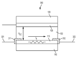
도 1은 몇몇 실시예들에 따른 액정 디바이스의 개략도이다;
도 2는 제 1 전극을 통해, 히터 전류(Ih)를 제공하도록 구성된 전압 소스를 포함하는 제어 시스템을 가진 액정 디바이스의 다이어그램이다;
도 3은 몇몇 실시예들에 따른 전극들 중 하나 상에 배치된 전기 컨택들을 포함한 액정 디바이스를 예시한다;
도 4는 몇몇 실시예들에 따른 줄(Joule) 가열을 제공하는 하나의 전극 및 하나의 접지 전극을 가진 디바이스를 예시한 개략도이다;
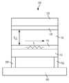
도 5는 몇몇 실시예들에 따른 히터 전극과 연관된 기판의 열 분리를 제공하는 액정 디바이스의 실시예를 예시한다;
도 6은 몇몇 실시예들에 따른 각각의 전극의 일 단부에서 인가된 전류 소스 및 각각의 전극의 반대 단부에서 연결된 전압 소스를 포함한 액정 디바이스를 도시한다;
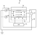
도 7은 액정 디바이스의 구성요소의 온도를 측정하도록 구성된 센서를 포함하는 피드백 제어 시스템을 포함한 액정 디바이스를 예시한다;
도 8a는 몇몇 실시예들에 따른 초분광 이미징 시스템을 예시한 블록도이다; 및
도 8b는 도 8a의 초분광 이미징 시스템의 액정 가변 지연판을 보다 상세하게 도시한다.1 is a schematic view of a liquid crystal device according to some embodiments;
Figure 2 is a diagram of a liquid crystal device with a control system comprising a voltage source configured to provide a heater current ( Ih ) through a first electrode;
Figure 3 illustrates a liquid crystal device including electrical contacts disposed on one of the electrodes according to some embodiments;
4 is a schematic diagram illustrating a device having one electrode and one ground electrode providing Joule heating in accordance with some embodiments;
5 illustrates an embodiment of a liquid crystal device that provides thermal isolation of a substrate associated with a heater electrode according to some embodiments;
Figure 6 illustrates a liquid crystal device including a current source applied at one end of each electrode and a voltage source connected at the opposite end of each electrode in accordance with some embodiments;
Figure 7 illustrates a liquid crystal device including a feedback control system including a sensor configured to measure the temperature of the components of the liquid crystal device;
8A is a block diagram illustrating an ultrasound imaging system in accordance with some embodiments; And
Figure 8b shows the liquid crystal variable delay plate of the ultra-spectral imaging system of Figure 8a in more detail.
온도는 액정(LC) 디바이스들의 성능에 강하게 영향을 주는 파라미터이다. LC 재료가 네마틱 상태인 온도의 범위가 있다. 많은 LC 디바이스들은 LC 디바이스가 네마틱 온도 범위 내에서 동작되도록 요구한다. 몇몇 LC 디바이스들은 LC 디바이스가 네마틱 온도 범위 내에 저장되도록 요구한다. 더욱이, 액정 성능 지수(FoM; Figure of Merit)에 의해 캡처된, 최적의 온도가 있으며, 고정된 양의 광 경로 지연이 최단 시간에(종속 파라미터로서 셀 두께를 갖고) 스위칭될 수 있다. 그러므로, 많은 LC 디바이스들은 적절한 또는 최적의 동작을 위해 온도 제어를 요구한다.Temperature is a parameter that strongly affects the performance of liquid crystal (LC) devices. There is a range of temperatures where the LC material is in a nematic state. Many LC devices require the LC device to operate within a nematic temperature range. Some LC devices require that the LC device be stored within a nematic temperature range. Furthermore, there is an optimum temperature captured by the liquid crystal figure of merit (FoM) and a fixed amount of optical path delay can be switched in the shortest time (with cell thickness as a dependent parameter). Therefore, many LC devices require temperature control for proper or optimal operation.
본 출원에서 논의된 실시예들은 저항성 가열을 통한 LC 디바이스들의 온도 제어에 관한 것이다. 액정 디바이스들은 일반적으로 몇몇 종류의 투명 전극, 예를 들면, 투명한 전도성 산화물 또는 얇은 금속 층을 포함한다. 표준 역평행 네마틱 LC 셀은 전극들 사이에 배치된 LC 재료를 가진 평행 판 커패시터와 비슷할 수 있다. 전극들은 LC 재료의 방위를 제어하기 위해 상이한 전압들로 구동되며, 주어진 전극의 모든 면적들은 그 외 동일한 전위인 것으로 가정된다. 본 출원에서 논의된 접근법들은 전극을 통해 전류를 전달함으로써 LC 재료에 대한 줄 히터로서 전극들 중 하나 이상의 사용을 수반하여, 다양한 구동 구성들 및 시간 시퀀스들을 고려한다. 이들 구성들에서, 동일한 전극의 상이한 포인트들에서의 전위는 상이할 수 있다.The embodiments discussed in this application relate to temperature control of LC devices through resistive heating. Liquid crystal devices generally include some kind of transparent electrode, for example a transparent conductive oxide or a thin metal layer. A standard antiparallel nematic LC cell may be similar to a parallel plate capacitor with an LC material disposed between the electrodes. The electrodes are driven at different voltages to control the orientation of the LC material, and all areas of a given electrode are assumed to be at the same other potential. The approaches discussed in this application involve the use of one or more of the electrodes as row heater for the LC material by transferring current through the electrodes, taking into account various drive arrangements and time sequences. In these configurations, the potential at the different points of the same electrode may be different.
LC 히터 및/또는 LC 온도 센서로서 LC 셀 전극을 사용함으로써, LC 히터 및/또는 LC 온도 센서가 LC 셀의 외부에 위치되는 경우보다 낮은 전력 소비 및/또는 보다 빠르고 보다 정확한 온도 제어가 달성될 수 있다. 더욱이, LC 셀을 구동하는 것 외에 가열 및 온도 감지를 위해 LC 셀 전극을 이용하는 것은 액정 디바이스들을 형성하기 위해 요구된 제조 프로세스들을 간소화하도록 돕는다. 이하에서 설명되는 실시예들은 액정 재료 온도를 제어하며 및/또는 방위 스위칭 시간을 감소시키기 위해 액정 재료들에 대한 온도 센서들 및 저항성 히터들과 같은 다수의 목적들을 위해 LC 셀 방위 제어 전극들을 사용하는 것을 수반한다.By using the LC cell electrode as the LC heater and / or LC temperature sensor, lower power consumption and / or faster and more accurate temperature control can be achieved than when the LC heater and / or LC temperature sensor is located outside the LC cell have. Moreover, besides driving the LC cell, using LC cell electrodes for heating and temperature sensing helps to simplify the manufacturing processes required to form liquid crystal devices. The embodiments described below use LC cell orientation control electrodes for a number of purposes such as temperature sensors and resistive heaters for liquid crystal materials to control liquid crystal material temperature and / or reduce orientation switching time .
도 1은 몇몇 실시예들에 따른 액정 디바이스(100)의 개략도이다. 디바이스(100)는 제 1 기판(110)의 표면(110a) 상에 배치된 제 1 전극(115)을 가진 제 1 기판(110) 및 제 1 전극(125)을 향하는 제 2 기판(120)의 표면(120a) 상에 배치된 제 2 전극(125)을 가진 제 2 기판(120)을 포함한다. 기판들(110, 120) 중 하나 또는 양쪽 모두는, 유리와 같은, 투명 재료로 만들어질 수 있다. 전극들(115, 125) 중 하나 또는 양쪽 모두는 전도성 산화물, 예로서 인듐 주석 산화물(ITO) 또는 얇은 금속 층과 같은 투명 도체로 만들어질 수 있다.1 is a schematic diagram of a
액정 재료(130)는 제 1 전극(115)과 제 2 전극(125) 사이에 배치된다. 제 1 및 제 2 전극들(115, 125)은 제 1 및 제 2 전극들(115, 125)에 걸쳐 인가된 전압이 액정 재료(130)의 방위를 제어하도록 배열된다. 제 1 및 제 2 전극들(115, 125)에 걸쳐 전압을 변경하는 것은 일반적으로 기판들(110, 120) 중 하나에 입사된 광 빔의 두 개의 직교 편광들 사이에서의 광 지연과 같은, LC 재료의 광 특성들을 변경한다.The
전극의 저항은 전류가 전극을 통과할 때 열의 형태로 전력을 소산시킨다. 전극을 통해 전류에 의해 발생된 저항성 열은 액정 재료를 가열시킨다. 본 출원에서 개시된 실시예들에서, 액정 재료(130)의 방위를 제어하기 위해 사용된 전극들(115, 125) 중 적어도 하나는 또한 액정 재료(130)를 저항성으로 가열하기 위해 사용된다. 적어도 하나의 전극은 LC 재료에 인접한 셀의 내부 내에 배치된다. The resistance of the electrode dissipates power in the form of heat as the current passes through the electrode. The resistive heat generated by the current through the electrode heats the liquid crystal material. In the embodiments disclosed in this application, at least one of the
도 1에 도시된 바와 같이, 디바이스(100)는, 전극(115)을 통해, 히터 전류(Ih)를 공급하도록 구성된 제어 시스템(140)을 포함한다. 제어 시스템(140)은 또한 제 1(115) 및 제 2(125) 전극들에 걸쳐 방위 제어 전압(VLC)을 공급하도록 구성될 수 있다. 몇몇 실시예들에 따르면, 제어 회로(140)는 스위치들, 센서들, 및/또는 제어 회로와 같은 전자 회로 및/또는 히터 전류를 위한 자동 개방 루프 제어 및/또는 폐쇄 루프 피드백 제어를 구현하도록 구성된 프로세서들을 포함한다.As shown in FIG. 1, the
도 2의 블록도에 도시된 LC 디바이스(200)에서, 제어 시스템(240)은 이 실시예에서 히터 전극으로서 작용하는 제 1 전극(115)을 통해, 히터 전류(Ih)를 제공하는 전압 소스(241)를 포함한다. 방위 제어 전압(VLC)은 LC 재료(130)의 방위를 제어하기 위해 제 1 및 제 2 전극들(115, 125)에 걸쳐 인가될 수 있다. In the
도 2의 LC 디바이스(200)는 제어된 바이어스가 전극(115)에 인가되는 전극(115)을 포함하며, 따라서 전류는 저항(R)을 갖고 전극(115)을 통해 흐른다. 예를 들면, LC 디바이스(200)가 1 ㎠의 면적 및 1 ㎟/s의 열 확산율(D)을 가진다면, 및 전압 소스(241)가 전극(115)에 걸쳐 전압(V)을 인가하면, 1초의 시간 기간 동안 줄 가열(V2/R)을 발생시키는 것((1s)ㆍV2/R 줄)은 대략 0.5g 양의 유리 및 부수적인 양의 LC 재료에 증착되어서, 줄(J) 당 약 2.5℃로 LC 재료(130)의 온도를 상승시킨다. 10℃ 온도 상승을 달성하기 위해, 그러므로 4J을 요구할 것이다. 제 1 전극(115)이 평방당 25옴(ohms)의 통상적인 시트 저항을 가진 인듐 주석 산화물(ITO)이면, 4J을 제공하는 것은 1초 시간 기간 동안 10V의 전압(및 400 mA의 전류)을 인가함으로써 가능하다. 이러한 시나리오는 액정 셀 히터 회로에 대한 적정한 범위 내에 있다.The
전극을 통한 전류의 분배는 전극의 어느 한 측으로의 전기 연결들의 위치에 의해 부분적으로 제어될 수 있다. 전극을 통해 흐르는 전류의 대체로 균일한 시트를 달성하기 위해, 고도의 전도성 재료, 예를 들면, 증발에 의해 증착된 얇은 금속 또는 금 층, 또는 금속성 페인트 또는 잉크가 소스로의 전기적 연결들이 이루어진 전극의 양쪽 측들 및/또는 에지들에 걸쳐 개별적으로 증착될 수 있다. 도 3에 예시된 바와 같이, 몇몇 구성들에서, LC 디바이스(300)는 제 1(115) 및 제 2(125) 전극들 중 하나 또는 양쪽 모두 상에 배치된 전기 컨택들(311, 312)을 포함할 수 있다. 전기 컨택들(311, 312)은 전극들(115, 125) 중 하나 또는 양쪽 모두에서 균일한 시트 히터 전류 밀도를 가능하게 하기 위해 전극들(115, 125)의 재료보다 높은 전도도를 가진 재료로 형성된다. 컨택들(311, 312)은 전극들(115, 125) 중 하나 또는 양쪽 모두 상에서의 둘 이상의 이격된 위치들에 배치될 수 있다. 몇몇 실시예들에서, 컨택들(311, 312)은 액정 재료(130)를 가열하기 위해 사용된 전류를 전달하는 전극(115) 상에서만 배치될 수 있다. 컨택들(311, 312)은 예를 들면, 전극들(115, 125) 상에 페인팅되거나 또는 인쇄되는 전도성 페인트 또는 잉크, 또는 패터닝된, 증발된 금속 막이거나 또는 이를 포함할 수 있다.The distribution of current through the electrodes can be partially controlled by the location of the electrical connections to either side of the electrode. In order to achieve a substantially uniform sheet of current flowing through the electrodes, a highly conductive material, such as a thin metal or gold layer deposited by evaporation, or a layer of metallic paint or ink, May be deposited individually on both sides and / or edges. 3, in some configurations, the
도 4는 몇몇 실시예들에 따른 줄 가열을 제공하는 하나의 전극(115) 및 하나의 접지 전극(125)을 가진 디바이스(400)를 예시한 개략도이다. 전압 소스(241)는 전극(115)을 통해 전류를 제공하기 위해 및/또는 LC 재료 방위를 제어하기 위해 사용될 수 있다.FIG. 4 is a schematic diagram illustrating a
도 4의 개략도에 도시된 바와 같이, 몇몇 실시예들에 따르면, LC 디바이스(400)의 제어 시스템(440)은 히터 전류를 제어하도록 구성된 적어도 하나의 스위치(445)를 포함한다. 제어 시스템(440)의 회로는 히터 전류(Ih)를 인가하거나 또는 히터 전극(115)으로부터 제거하기 위해 폐쇄 또는 개방 구성으로 스위치(445)를 동작시키도록 구성될 수 있다. 제어 시스템(440)은 전극(115)을 통해 히터 전류를 발생시키는 전압 및 LC 재료의 방위를 제어하는 전압 사이에서 시간 다중화하도록 스위치(445)를 동작시킬 수 있다. 제어 시스템(400)은 스위치(445)가 개방될 때 방위 제어 전압을 인가한다. 이러한 구성에서, 제 1 전극(115)에 걸쳐 대체로 균일한 전위가 있다. 스위치(445)가 폐쇄될 때, 전압 소스(241)에 의한 전압의 인가는 전극(115)을 통과하는 전류를 생성하며 그러므로 전극(115)에 걸쳐 전위 기울기를 생성한다.4, according to some embodiments, the
몇몇 구현들에서, 제어 시스템(440)은 펄스화된 히터 전류를 제공하도록 스위치(445)를 동작시킨다. 방위 제어 전압 및 히터 전류의 인가 사이에서 전위 간섭을 감소시키기 위해 히터 전류 펄스들의 지속 기간을 제한하는 것이 유용할 수 있다. 간섭에 대한 감소된 전위를 가진 최적의 가열을 제공하기 위해, 전류 펄스들의 지속 기간은 전극의 열 시상수들, 액정 재료, 및 인접한 기판들 또는 히터 전극에 근접한 인접한 기판들의 적어도 일 부분의 열 시상수들에 기초하여 선택될 수 있다. 몇몇 실시예들에서, 펄스들의 듀티 사이클은 약 10% 미만, 약 5% 미만, 또는 심지어 약 1% 미만이다. LC 디바이스를 사용하는 듀티 사이클 또는 순환 시간이 비교적 낮다면(예로서, 분당 1초 동안 가열), LC 디바이스는 사용들 사이에서 냉각시키도록 허용될 수 있다.In some implementations, the
대안적으로, 듀티 사이클이 더 높다면, 그것을 보다 큰 시스템에 기계적으로 통합하는 열 절연 스탠드오프들 상에 LC 디바이스를 장착시킴으로써 LC 디바이스를 열적 분리하는 것이 이해가 될 수 있다. LC 디바이스를 열적 분리하는 것은 주변 구조에 대한 보다 적은 열 손실을 야기할 수 있다. 예를 들면, 주변 구조는 LC 디바이스의 하우징, 프레임 및/또는 다른 지지 부재들을 포함할 수 있다.Alternatively, if the duty cycle is higher, it may be understandable to thermally isolate the LC device by mounting the LC device on the thermal isolation standoffs that mechanically integrates it into a larger system. Thermal separation of the LC device may result in less heat loss to the surrounding structure. For example, the peripheral structure may comprise a housing, frame and / or other support members of the LC device.
도 5는 히터 전극과 연관된 기판의 열적 분리를 제공하는 LC 디바이스(500)의 실시예를 예시한다. 액정 디바이스(500)는 열적 분리 재료로 만들어진 스탠드오프들(551, 552)을 포함한다. 스탠드오프들(551, 552)은 히터 전류(Ih)를 나르는 전극(115)과 연관된 기판(110), 및 LC 디바이스(500)의 주변 구조(550) 사이에 배치된다. 스탠드오프들(551, 552)은 그것들이 LC 디바이스의 또렷한 애퍼처를 가리지 않도록 배열될 수 있다. Figure 5 illustrates an embodiment of an
이제 도 4로 돌아가면, LC 디바이스(400)는 히터 전극(115)을 통해 전압 소스(241)에 전기적으로 결합된 스위치(445)를 통해 히터 전류를 제어하도록 구성된 제어 시스템(440)을 포함한다. 제어 시스템(400)은 제 1 및 제 2 전극들(115, 125)에 걸쳐 방위 제어 전압을 인가하는 것 및 전극(115)을 통해 전류를 발생시키는 전압을 인가하는 것 사이에서의 충돌을 중재하기 위해 시간-다중화 프로토콜을 적용할 수 있다. 제어 시스템(400)은 스위치(445)가 개방될 때 전압 소스(241)에서 방위 제어 전압을 인가한다. 스위치(445)가 폐쇄될 때, 전압 소스(241)에 의해 인가된 전압은 전극(115)을 통과하는 전류를 생성한다. 그러나, 이러한 시나리오에서, 히터 전극(115)에 걸친 바람직하지 않은 전압 강하가 존재하며 문제가 될 수 있다.4, the
바람직하지 않은 전압 강하를 바로잡기 위한 방식은 도 6에 개략적으로 도시된 LC 디바이스(600)의 제어 시스템(640)에 의해 제공된다. 도 6의 디바이스는 각각의 전극의 일 단부에 인가된 전류 소스 및 각각의 전극의 반대 단부에 인가된 전압 소스를 포함한다. 제어 시스템(640)은 두 개의 전류 소스들(642, 643)을 제어한다. 각각의 전류 소스(642, 643)는 전류(I)를 제공한다. 전류 소스(642)는 제 1 전극(115)의 제 1 위치, 예로서 제 1 에지에 전기적으로 연결되며 전류 소스(643)는 제 2 전극(125)의 제 1 위치, 예로서 제 1 에지에 전기적으로 연결된다. 제 1 및 제 2 전극들(115, 125)의 각각은 에지 저항(R)과 대체로 동일한 에지를 가질 수 있다. 그러므로, 단부에서 단부로의 각각의 전극(115, 125)에 걸친 전압 강하는 I*R이다. 제 1 전극(115)에서 제 2 전극(125)으로의 전압 강하는 전압(V)을 제공하는 전압 소스(641)에 의해 제어된다. 제 1 전극(115)으로부터 제 2 전극(125)으로의 이러한 전압 강하는 제 1 전극(115)으로부터 제 2 전극(125)까지의 임의의 수직 라인에 걸쳐 동일할 것이다. 따라서, 전기장은 액정 재료(130) 내에서 대체로 균일하여, 그것의 방위가 가열에 독립적으로 제어되도록 허용한다. 스위치(645)는 전류가 전극들(115, 125)을 통해 흐르는지를 제어하기 위해 사용될 수 있다. 도 6에 도시된 구성은 각각의 전극에 걸쳐 최소의 바람직하지 않은 전압 강하를 가진 가열 및 방위 제어 양쪽 모두를 제공할 수 있는 많은 회로 구성들 중 하나임을 주의하자. 이들 회로 구성들은 본 출원에서 설명된 접근법들 내에 포함되는 것으로 고려된다.A scheme for correcting undesirable voltage drops is provided by the
도 7의 개략도에 도시된 바와 같이, 몇몇 실시예들에서 LC 디바이스(700)는 가열 전극, 액정 재료, 또는 다른 LC 디바이스 구성요소의 온도를 측정하도록 구성된 센서(760)를 포함하는 피드백 제어 시스템(740)을 포함한다. 온도 측정은 LC 재료를 가열하기 위해 인가된 전류를 제어하기 위한 피드백 신호를 제공하기 위해 제어 시스템(740)에 의해 사용될 수 있다.7, in some embodiments, the
몇몇 실시예들에서, 온도 센서는 LC 디바이스의 전극, LC 재료, 및/또는 다른 구성요소들의 저항을 측정하는 4 포인트 프로브를 포함할 수 있다. 측정된 재료의 알려진 저항 온도 계수로 인해, 저항 측정은 온도의 대리 측정을 제공하며 히터 전류를 제어하기 위해 사용될 수 있다. 도 7은 제 1 전극(115)의 저항(R)의 4-포인트 저항 측정 구성을 도시하며, 그에 의해 전류는 전류 소스(642)에 의해 전극(115)을 통해 제공되며, 전압은 센서(760)에 의해 측정된다. 4 포인트 저항 측정은 원하는 온도를 달성하기 위해, 저항(R)의 정확한 독출을 제공하며 따라서 히터 전류(I)를 제어하기 위해 제어 시스템(740)에 의해 사용될 수 있는 온도 측정에 대한 대리이다. 이러한 접근법은, 적어도 감지 요소가 LC 재료에 가깝기 때문에, 다른 방법들에 비교하여 강화된 측정 정확도를 제공한다.In some embodiments, the temperature sensor may include a 4-point probe that measures the resistance of the electrodes, LC material, and / or other components of the LC device. Due to the known resistance temperature coefficient of the measured material, the resistance measurement provides a surrogate measurement of temperature and can be used to control the heater current. 7 shows a 4-point resistance measurement configuration of the resistance R of the
본 출원에서 논의된 바와 같이 LC 디바이스는 도 8a의 블록도에 도시된 바와 같이 초분광 이미징 시스템(800)을 위한 스펙트럼 인코더에서 가변 광 지연판으로서 특히 유용하다. 도 8a의 초분광 이미저(800)는 이미지 센서(830)와 조합하여 본 출원에서 설명된 바와 같이 저항성 가열을 사용하여 제어된 온도인 액정(LC) 스펙트럼 인코더(810)에 기초한다. 도 8a에 도시되고 도 8b에서 보다 상세하게 도시된 LC 스펙트럼 인코더(810)는 공통 경로를 통하지만 두 개의 직교 편광들을 갖고 이동하는 간섭 광에 의해 이미지에서의 각각의 포인트에서 인터페로그램으로 스펙트럼 정보를 인코딩한다. 제 1 편광기(811)는 입사 편광 방향으로, 공칭 LC 셀(810a)의 러빙(정렬) 방향에 대해 45도로 인입 광을 편광시킨다. 도 8a 및 도 8b에 도시된 LC 셀(810a)은 제 1(812) 전극과 제 2(814) 전극 사이에 배치된 제 1 LC 재료(813) 및 제 2(814) 전극과 제 3(816) 전극 사이에 배치된 제 2 LC 재료(815)를 포함하는 이중 네마틱 구조이다. 이중 네마틱 구조에서, LC 셀(810a)의 제 1 절반은 LC 셀(810a)의 제 2 절반에 대하여 미러링되며 제 1 절반은 제 1 LC 재료(813)를 포함하고 제 2 절반은 제 2 LC 재료(815)를 포함한다. 제 1 LC 재료(813) 및 제 2 LC 재료(815)의 두께는 몇몇 실시예들에서 대략 동일할 수 있다. 이중 네마틱 배열은 이상 광선 및 정상 광선의 상대 경로 지연으로 하여금 그것들이 LC 셀(810a)의 양쪽 절반들 모두를 통해 이동함에 따라 증가하게 하지만, LC 셀(810a)의 제 1 절반의 1차 각도 의존성은 LC 셀(810a)의 제 2 절반의 1차 각도 의존성에 의해 무효화된다.As discussed in this application, the LC device is particularly useful as a variable light retarder in a spectral encoder for the
LC 셀의 러빙 방향은 도 8b에서 각각의 전극(812, 814, 816) 상에서 화살표로 표시되며 LC 재료의 분자들이 향하는 선호 방향이다. 따라서, 전극들(812, 814, 186) 상에서의 화살표들 또는 방향으로 편광된 광(이상 광선 또는 e-선)은 직교하여 편광된 광(정상 광선 또는 o-선)에 대하여 지연될 것이다. LC 셀(810a)은 전기적 동조 가능 복굴절 요소로서 기능한다. LC 셀(810a)에 걸쳐 전압을 변경함으로써, LC 분자들은 그것들의 방위를 변경하며, e-선 및 o-선 사이에 가변 광 경로 지연을 생성하는 것이 가능하다. 이러한 경로 지연은 두 개의 광선들 사이에서 파장-의존적 위상 시프트를 야기하며, 그에 의해 편광 상태에서 파장-의존적 변화를 야기한다.The rubbing direction of the LC cell is indicated by the arrows on each
제 1 편광기에 평행하거나 또는 수직으로 방위된, 제 2 편광기(817), 또는 분석기는 두 개의 광선들을 간섭함으로써 파장-의존적 강도 패턴으로 이러한 파장-의존적 편광 상태를 변경한다. 강도 패턴(경로 지연의 함수로서)은 마이켈슨(Michelson) 간섭계에 의해 생성된 인터페로그램과 같다. 따라서, 강도 패턴은 입사된 광의 스펙트럼의 코사인 변환에 대응한다. LC 셀(810a) 상에서의 전압이 제어기(819)에 의해 변경됨에 따라 일련의 이미지들을 기록함으로써, 이미지에서의 모든 포인트들에서의 인터페로그램들이 동시에 샘플링될 수 있으며, 초분광 데이터-큐브가 광 경로 지연 축을 따라 역 코사인 변환에 의해 복원될 수 있다.A
제어기(819)는 전극들(812 및 814)에 걸쳐 인가된 전압을 변경함으로써 제 1 LC 재료(813)의 방위를 변경할 수 있으며 전극(814 및 816)에 걸쳐 인가된 전압을 변경함으로써 제 2 LC 재료(816)의 방위를 변경할 수 있다. 제어기(819)는 이전에 설명된 바와 같이 전극들(812, 814, 816) 중 하나 이상을 통해 전류를 전달함으로써 저항성 가열을 통해 LC 재료(815)의 온도를 제어할 수 있다. The
Claims (10)
제 1 투명 기판;
상기 제 1 투명 기판의 표면상에 배치된 제 1 투명 전극;
제 2 기판;
상기 제 1 투명 전극을 향하는 상기 제 2 기판의 표면상에 배치된 제 2 전극;
상기 제 1 전극과 제 2 전극 사이에 배치된 액정 재료로서, 상기 제 1 전극과 제 2 전극 사이에 인가된 전압이 상기 액정 재료의 방위를 제어하는, 상기 액정 재료; 및
상기 액정 재료를 저항성으로(resistively) 가열하기 위해 상기 제 1 및 제 2 전극들 중 적어도 하나의 전극을 통해 전기 전류를 인가하도록 구성된 제어 시스템을 포함하는, 디바이스. In a device,
A first transparent substrate;
A first transparent electrode disposed on a surface of the first transparent substrate;
A second substrate;
A second electrode disposed on a surface of the second substrate facing the first transparent electrode;
A liquid crystal material disposed between the first electrode and the second electrode, wherein a voltage applied between the first electrode and the second electrode controls the orientation of the liquid crystal material; And
And a control system configured to apply an electrical current through at least one of the first and second electrodes to resistively heat the liquid crystal material.
상기 제 2 기판 및 상기 제 2 전극은 투명한, 디바이스.The method according to claim 1,
Wherein the second substrate and the second electrode are transparent.
상기 적어도 하나의 전극 상에 배치된 제 1 및 제 2 이격된 전기 컨택(contact)들을 더 포함하며, 상기 제 1 및 제 2 전기 컨택들은 상기 적어도 하나의 전극보다 높은 전도도를 갖는, 디바이스.The method according to claim 1,
Further comprising first and second spaced electrical contacts disposed on the at least one electrode, wherein the first and second electrical contacts have a higher conductivity than the at least one electrode.
상기 제 1 및 제 2 전극들 중 하나 또는 양쪽 모두는 전도성 산화물을 포함하는, 디바이스.The method according to claim 1,
Wherein one or both of the first and second electrodes comprise a conductive oxide.
상기 전기 전류는 펄스화된(pulsed) 전류인, 디바이스.
상기 액정 재료의 방위를 제어하기 위한 전극 및 상기 액정 재료를 저항성으로 가열하기 위해 상기 적어도 하나의 전극을 통해 전류를 제어하도록 구성된 가열 제어 회로The method according to claim 1,
Wherein the electrical current is a pulsed current.
An electrode for controlling the orientation of the liquid crystal material and a heating control circuit configured to control current through the at least one electrode to resistively heat the liquid crystal material;
제 1 편광기;
제 2 편광기;
상기 제 1 편광기와 상기 제 2 편광기 사이에 배치된 액정 가변 지연판으로서:
제 1 투명 기판;
상기 제 1 투명 기판의 표면상에 배치된 제 1 투명 전극;
제 2 투명 전극;
상기 제 1 투명 전극을 향하는 상기 제 2 투명 기판의 표면상에 배치된 제 2 투명 전극; 및
상기 제 1 전극과 상기 제 2 전극 사이에 배치된 액정 재료로서, 상기 제 1 및 제 2 전극들은 상기 제 1 전극 및 상기 제 2 전극 사이에 인가된 전압이 상기 액정 재료의 방위를 제어하며 상기 제 1 및 제 2 전극들 중 적어도 하나의 전극을 통해 인가된 전기 전류가 상기 액정 재료를 저항성으로 가열하도록 배열된, 상기 액정 재료를 포함하는, 상기 액정 가변 지연판; 및
상기 제 2 편광기로부터 광을 수신하도록 배열된 이미지 센서를 포함하는, 초분광 이미징 시스템.In an ultrasound imaging system,
A first polarizer;
A second polarizer;
A liquid crystal variable delay plate disposed between the first polarizer and the second polarizer,
A first transparent substrate;
A first transparent electrode disposed on a surface of the first transparent substrate;
A second transparent electrode;
A second transparent electrode disposed on the surface of the second transparent substrate facing the first transparent electrode; And
A liquid crystal material disposed between the first electrode and the second electrode, wherein a voltage applied between the first electrode and the second electrode controls the orientation of the liquid crystal material, The liquid crystal material being arranged such that an electric current applied through at least one of the first and second electrodes resistively heating the liquid crystal material; And
And an image sensor arranged to receive light from the second polarizer.
상기 제 1 전극 및 상기 제 2 전극에 전기적으로 결합된 제어 시스템을 더 포함하며, 상기 제어 시스템은 상기 액정 재료의 방위를 제어하기 위해 상기 전압을 제공하고 상기 액정 재료를 가열하기 위해 상기 적어도 하나의 전극을 통해 상기 전기 전류를 제공하도록 구성된, 초분광 이미징 시스템.The method of claim 6,
Further comprising a control system electrically coupled to the first electrode and the second electrode, wherein the control system provides the voltage to control the orientation of the liquid crystal material and the at least one And configured to provide the electrical current through an electrode.
상기 제 1 전극과 상기 제 2 전극 사이에서 전압을 제어함으로써 상기 액정 재료의 방위를 제어하는 단계; 및
상기 제 1 및 제 2 전극들 중 적어도 하나의 전극을 통해 전기 전류를 제어함으로써 상기 액정 재료를 저항성으로 가열하는 단계를 포함하는, 액정 셀을 제어하는 방법.A method of controlling a liquid crystal cell including a first transparent electrode, a second transparent electrode, and a liquid crystal material disposed between the first electrode and the second electrode,
Controlling the orientation of the liquid crystal material by controlling a voltage between the first electrode and the second electrode; And
And resistively heating the liquid crystal material by controlling an electric current through at least one of the first and second electrodes.
상기 적어도 하나의 전극을 통해 상기 전기 전류를 제어하는 단계는 펄스화된 전기 전류를 공급하는 단계를 포함하는, 액정 셀을 제어하는 방법.The method of claim 8,
Wherein controlling the electrical current through the at least one electrode comprises supplying a pulsed electrical current.
상기 액정 재료의 온도를 감지하는 단계; 및
감지된 상기 온도에 응답하여 상기 저항성 가열을 제어하는 단계를 더 포함하는, 액정 셀을 제어하는 방법.The method of claim 8,
Sensing a temperature of the liquid crystal material; And
Controlling the resistive heating in response to the sensed temperature. ≪ Desc / Clms Page number 21 >
Priority Applications (1)
| Application Number | Priority Date | Filing Date | Title |
|---|---|---|---|
| KR1020220185004A KR102612631B1 (en) | 2017-10-24 | 2022-12-26 | Liquid crystal temperature control by resistive heating |
Applications Claiming Priority (2)
| Application Number | Priority Date | Filing Date | Title |
|---|---|---|---|
| US15/792,465 | 2017-10-24 | ||
| US15/792,465 US10884278B2 (en) | 2017-10-24 | 2017-10-24 | Liquid crystal temperature control by resistive heating |
Related Child Applications (1)
| Application Number | Title | Priority Date | Filing Date |
|---|---|---|---|
| KR1020220185004A Division KR102612631B1 (en) | 2017-10-24 | 2022-12-26 | Liquid crystal temperature control by resistive heating |
Publications (1)
| Publication Number | Publication Date |
|---|---|
| KR20190045832A true KR20190045832A (en) | 2019-05-03 |
Family
ID=63965421
Family Applications (2)
| Application Number | Title | Priority Date | Filing Date |
|---|---|---|---|
| KR1020180119731A KR20190045832A (en) | 2017-10-24 | 2018-10-08 | Liquid crystal temperature control by resistive heating |
| KR1020220185004A KR102612631B1 (en) | 2017-10-24 | 2022-12-26 | Liquid crystal temperature control by resistive heating |
Family Applications After (1)
| Application Number | Title | Priority Date | Filing Date |
|---|---|---|---|
| KR1020220185004A KR102612631B1 (en) | 2017-10-24 | 2022-12-26 | Liquid crystal temperature control by resistive heating |
Country Status (5)
| Country | Link |
|---|---|
| US (1) | US10884278B2 (en) |
| EP (1) | EP3477367A1 (en) |
| JP (1) | JP7166126B2 (en) |
| KR (2) | KR20190045832A (en) |
| CN (1) | CN109696765A (en) |
Families Citing this family (10)
| Publication number | Priority date | Publication date | Assignee | Title |
|---|---|---|---|---|
| US10564504B2 (en) * | 2017-11-30 | 2020-02-18 | Palo Alto Research Center Incorporated | Liquid-crystal variable retarder using liquid crystal cells of differing thicknesses |
| US10983338B2 (en) | 2017-12-29 | 2021-04-20 | Palo Alto Research Center Incorporated | Exit-pupil expander used distribute light over a liquid-crystal variable retarder |
| US10663346B2 (en) | 2017-12-29 | 2020-05-26 | Palo Alto Research Center Incorporated | Method and apparatus for transforming uniformly or non-uniformly sampled interferograms to produce spectral data |
| CN108267450A (en) * | 2018-02-28 | 2018-07-10 | 京东方科技集团股份有限公司 | Substrate detection apparatus and method |
| CN108983476B (en) * | 2018-08-31 | 2021-09-07 | 上海天马微电子有限公司 | Liquid crystal display panel and liquid crystal display device |
| US11567179B2 (en) | 2020-07-21 | 2023-01-31 | Leddartech Inc. | Beam-steering device particularly for LIDAR systems |
| WO2022016277A1 (en) | 2020-07-21 | 2022-01-27 | Leddartech Inc. | Systems and methods for wide-angle lidar using non-uniform magnification optics |
| CA3194223A1 (en) | 2020-07-21 | 2021-10-06 | Leddartech Inc. | Beam-steering device particularly for lidar systems |
| WO2022155612A1 (en) * | 2021-01-18 | 2022-07-21 | Boulder Nonlinear Systems, Inc. | Aperture heating for liquid crystal beam steering systems |
| CN113156673B (en) * | 2021-04-09 | 2023-02-28 | Tcl华星光电技术有限公司 | Alignment detection device and detection method thereof |
Family Cites Families (27)
| Publication number | Priority date | Publication date | Assignee | Title |
|---|---|---|---|---|
| JPH0621907B2 (en) * | 1985-09-26 | 1994-03-23 | 株式会社日立製作所 | Driving method for liquid crystal display |
| US4773735A (en) | 1986-08-04 | 1988-09-27 | Allied-Signal Inc. | Fast warm-up heater for liquid crystal display |
| US4987289A (en) | 1988-07-21 | 1991-01-22 | Rockwell International Corporation | Liquid crystal display heating system |
| JPH04271323A (en) * | 1991-02-27 | 1992-09-28 | Fuji Photo Film Co Ltd | Liquid crystal display element |
| JPH05127153A (en) * | 1991-10-31 | 1993-05-25 | Canon Inc | Transparent panel heater |
| JPH0736414A (en) * | 1993-07-20 | 1995-02-07 | Sharp Corp | Controller for liquid crystal display voltage |
| US5805117A (en) * | 1994-05-12 | 1998-09-08 | Samsung Electronics Co., Ltd. | Large area tiled modular display system |
| JPH10123527A (en) * | 1996-10-24 | 1998-05-15 | Canon Inc | Production of liquid crystal element |
| US6089751A (en) * | 1996-12-30 | 2000-07-18 | Honeywell Inc. | Transparent temperature sensor for an active matrix liquid crystal display |
| JPH11271711A (en) * | 1998-03-25 | 1999-10-08 | Citizen Watch Co Ltd | Power source control circuit for driving liquid crystal |
| JP3973477B2 (en) * | 2002-04-12 | 2007-09-12 | シャープ株式会社 | Image display device |
| JP2003329999A (en) | 2002-05-14 | 2003-11-19 | Toyota Industries Corp | Liquid crystal display device |
| US6943768B2 (en) * | 2003-02-21 | 2005-09-13 | Xtellus Inc. | Thermal control system for liquid crystal cell |
| US20050041020A1 (en) * | 2003-06-17 | 2005-02-24 | Cubic Corporation | Wide temperature range PDLC shutter |
| KR101131268B1 (en) | 2004-12-29 | 2012-03-30 | 엘지디스플레이 주식회사 | Liquid crystal display device |
| JP4919607B2 (en) | 2005-02-28 | 2012-04-18 | オプトレックス株式会社 | Liquid crystal display |
| US8562871B2 (en) * | 2006-07-10 | 2013-10-22 | Sabic Innovative Plastics Ip B.V. | Composition and associated method |
| WO2008017316A1 (en) | 2006-08-08 | 2008-02-14 | Gm Global Technology Operations, Inc. | Thermally tunable liquid crystal based optical correcting element for a display |
| JP2008083217A (en) * | 2006-09-26 | 2008-04-10 | Seiko Epson Corp | Liquid crystal device |
| JP5134286B2 (en) | 2007-05-18 | 2013-01-30 | 株式会社ジャパンディスプレイイースト | Liquid crystal display |
| KR101551519B1 (en) * | 2009-01-30 | 2015-09-09 | 알파마이크론, 인크. | Attachable optical element arrangements and methods |
| EP2718962A1 (en) * | 2011-06-10 | 2014-04-16 | Massachusetts Institute Of Technology | High-concentration active doping in semiconductors and semiconductor devices produced by such doping |
| AU2014212124A1 (en) * | 2013-02-01 | 2015-09-10 | Daniel FARKAS | Method and system for characterizing tissue in three dimensions using multimode optical measurements |
| CN105408815A (en) * | 2013-03-15 | 2016-03-16 | 兰斯维克托公司 | Methods and apparatus for focus improvement in multiple liquid crystal cell lenses |
| JP6443977B2 (en) | 2015-01-30 | 2018-12-26 | 京セラ株式会社 | Liquid crystal display |
| EP3203309A1 (en) * | 2016-02-04 | 2017-08-09 | Bodle Technologies Limited | Optical device with thermally switching phase change material |
| US10768497B2 (en) * | 2016-10-03 | 2020-09-08 | Xerox Corporation | Hyperspectral imaging system |
-
2017
- 2017-10-24 US US15/792,465 patent/US10884278B2/en active Active
-
2018
- 2018-09-30 CN CN201811153644.9A patent/CN109696765A/en active Pending
- 2018-10-01 JP JP2018186300A patent/JP7166126B2/en active Active
- 2018-10-08 KR KR1020180119731A patent/KR20190045832A/en not_active IP Right Cessation
- 2018-10-23 EP EP18202137.8A patent/EP3477367A1/en active Pending
-
2022
- 2022-12-26 KR KR1020220185004A patent/KR102612631B1/en active IP Right Grant
Also Published As
| Publication number | Publication date |
|---|---|
| EP3477367A1 (en) | 2019-05-01 |
| US10884278B2 (en) | 2021-01-05 |
| KR20230007997A (en) | 2023-01-13 |
| JP7166126B2 (en) | 2022-11-07 |
| KR102612631B1 (en) | 2023-12-14 |
| US20190121191A1 (en) | 2019-04-25 |
| JP2019079036A (en) | 2019-05-23 |
| CN109696765A (en) | 2019-04-30 |
Similar Documents
| Publication | Publication Date | Title |
|---|---|---|
| KR102612631B1 (en) | Liquid crystal temperature control by resistive heating | |
| JP2019079036A5 (en) | ||
| KR102430145B1 (en) | Liquid-crystal variable retarder using liquid crystal cells of differing thicknesses | |
| US3215038A (en) | Solid solution electro-optic light switch using the stark effect | |
| Liu et al. | Temperature control of terahertz metamaterials with liquid crystals | |
| EP3486716A1 (en) | Liquid crystal grating and control method therefor | |
| Zangeneh Kamali et al. | Electrically programmable solid-state metasurfaces via flash localised heating | |
| JP2002243555A (en) | Transparent surface temperature sensor and transparent surface temperature control device | |
| EP1136993A4 (en) | Optical head | |
| CN102017337A (en) | Method and system for fine adjustment of optical elements position | |
| CN112432904B (en) | Novel liquid crystal polarization modulator and detection method thereof | |
| JP4819415B2 (en) | Optical device | |
| CN112525493A (en) | Method and device for detecting optical characteristics of ferroelectric liquid crystal retarder | |
| KR100350537B1 (en) | Liquid crystal display device having enhanced operation ability in relatively low temperature | |
| Tatsumi et al. | Reduction of ambient temperature dependence of KTa1-xNbxO3 electro-optic deflector by double-thermistor structure | |
| GB2126365A (en) | A method of heating an electrooptical device | |
| US9813644B1 (en) | Nano-antenna array infrared imager | |
| US9766422B1 (en) | Optical membrane heating and temperature control method and apparatus | |
| Kato et al. | Characteristics of a ferroelectric liquid crystal spatial light modulator with a dielectric mirror | |
| JP2009133850A (en) | Polarization modulator and measuring apparatus | |
| Takeda et al. | Birefringence and electro-optic effect in epitaxial BST thin films | |
| JPS61187625A (en) | Temperature sensor | |
| JP2005221984A5 (en) | ||
| Baumann | Potassium dihydrogen phosphate and potassium tantalate niobate pyroelectric materials and far-infrared detectors | |
| Lee et al. | A High-Speed Optical Remote-Control Switch Based on Giant Persistent Photoconductivity |
Legal Events
| Date | Code | Title | Description |
|---|---|---|---|
| AMND | Amendment | ||
| E902 | Notification of reason for refusal | ||
| AMND | Amendment | ||
| E601 | Decision to refuse application | ||
| AMND | Amendment | ||
| X601 | Decision of rejection after re-examination |