KR20180118480A - Projection device using micro-led panel and method for fabricating the same - Google Patents
Projection device using micro-led panel and method for fabricating the same Download PDFInfo
- Publication number
- KR20180118480A KR20180118480A KR1020170051879A KR20170051879A KR20180118480A KR 20180118480 A KR20180118480 A KR 20180118480A KR 1020170051879 A KR1020170051879 A KR 1020170051879A KR 20170051879 A KR20170051879 A KR 20170051879A KR 20180118480 A KR20180118480 A KR 20180118480A
- Authority
- KR
- South Korea
- Prior art keywords
- micro led
- led panel
- light
- wavelength
- pixels
- Prior art date
Links
Images


Classifications
-
- G—PHYSICS
- G03—PHOTOGRAPHY; CINEMATOGRAPHY; ANALOGOUS TECHNIQUES USING WAVES OTHER THAN OPTICAL WAVES; ELECTROGRAPHY; HOLOGRAPHY
- G03B—APPARATUS OR ARRANGEMENTS FOR TAKING PHOTOGRAPHS OR FOR PROJECTING OR VIEWING THEM; APPARATUS OR ARRANGEMENTS EMPLOYING ANALOGOUS TECHNIQUES USING WAVES OTHER THAN OPTICAL WAVES; ACCESSORIES THEREFOR
- G03B21/00—Projectors or projection-type viewers; Accessories therefor
- G03B21/14—Details
- G03B21/20—Lamp housings
- G03B21/2006—Lamp housings characterised by the light source
- G03B21/2033—LED or laser light sources
- G03B21/204—LED or laser light sources using secondary light emission, e.g. luminescence or fluorescence
-
- G—PHYSICS
- G03—PHOTOGRAPHY; CINEMATOGRAPHY; ANALOGOUS TECHNIQUES USING WAVES OTHER THAN OPTICAL WAVES; ELECTROGRAPHY; HOLOGRAPHY
- G03B—APPARATUS OR ARRANGEMENTS FOR TAKING PHOTOGRAPHS OR FOR PROJECTING OR VIEWING THEM; APPARATUS OR ARRANGEMENTS EMPLOYING ANALOGOUS TECHNIQUES USING WAVES OTHER THAN OPTICAL WAVES; ACCESSORIES THEREFOR
- G03B21/00—Projectors or projection-type viewers; Accessories therefor
- G03B21/14—Details
- G03B21/20—Lamp housings
- G03B21/2006—Lamp housings characterised by the light source
- G03B21/2033—LED or laser light sources
-
- G—PHYSICS
- G03—PHOTOGRAPHY; CINEMATOGRAPHY; ANALOGOUS TECHNIQUES USING WAVES OTHER THAN OPTICAL WAVES; ELECTROGRAPHY; HOLOGRAPHY
- G03B—APPARATUS OR ARRANGEMENTS FOR TAKING PHOTOGRAPHS OR FOR PROJECTING OR VIEWING THEM; APPARATUS OR ARRANGEMENTS EMPLOYING ANALOGOUS TECHNIQUES USING WAVES OTHER THAN OPTICAL WAVES; ACCESSORIES THEREFOR
- G03B21/00—Projectors or projection-type viewers; Accessories therefor
- G03B21/14—Details
- G03B21/20—Lamp housings
- G03B21/2006—Lamp housings characterised by the light source
- G03B21/2013—Plural light sources
-
- G—PHYSICS
- G03—PHOTOGRAPHY; CINEMATOGRAPHY; ANALOGOUS TECHNIQUES USING WAVES OTHER THAN OPTICAL WAVES; ELECTROGRAPHY; HOLOGRAPHY
- G03B—APPARATUS OR ARRANGEMENTS FOR TAKING PHOTOGRAPHS OR FOR PROJECTING OR VIEWING THEM; APPARATUS OR ARRANGEMENTS EMPLOYING ANALOGOUS TECHNIQUES USING WAVES OTHER THAN OPTICAL WAVES; ACCESSORIES THEREFOR
- G03B33/00—Colour photography, other than mere exposure or projection of a colour film
- G03B33/10—Simultaneous recording or projection
- G03B33/12—Simultaneous recording or projection using beam-splitting or beam-combining systems, e.g. dichroic mirrors
-
- H—ELECTRICITY
- H01—ELECTRIC ELEMENTS
- H01L—SEMICONDUCTOR DEVICES NOT COVERED BY CLASS H10
- H01L27/00—Devices consisting of a plurality of semiconductor or other solid-state components formed in or on a common substrate
- H01L27/15—Devices consisting of a plurality of semiconductor or other solid-state components formed in or on a common substrate including semiconductor components with at least one potential-jump barrier or surface barrier specially adapted for light emission
- H01L27/153—Devices consisting of a plurality of semiconductor or other solid-state components formed in or on a common substrate including semiconductor components with at least one potential-jump barrier or surface barrier specially adapted for light emission in a repetitive configuration, e.g. LED bars
- H01L27/156—Devices consisting of a plurality of semiconductor or other solid-state components formed in or on a common substrate including semiconductor components with at least one potential-jump barrier or surface barrier specially adapted for light emission in a repetitive configuration, e.g. LED bars two-dimensional arrays
-
- H—ELECTRICITY
- H01—ELECTRIC ELEMENTS
- H01L—SEMICONDUCTOR DEVICES NOT COVERED BY CLASS H10
- H01L33/00—Semiconductor devices with at least one potential-jump barrier or surface barrier specially adapted for light emission; Processes or apparatus specially adapted for the manufacture or treatment thereof or of parts thereof; Details thereof
- H01L33/02—Semiconductor devices with at least one potential-jump barrier or surface barrier specially adapted for light emission; Processes or apparatus specially adapted for the manufacture or treatment thereof or of parts thereof; Details thereof characterised by the semiconductor bodies
- H01L33/04—Semiconductor devices with at least one potential-jump barrier or surface barrier specially adapted for light emission; Processes or apparatus specially adapted for the manufacture or treatment thereof or of parts thereof; Details thereof characterised by the semiconductor bodies with a quantum effect structure or superlattice, e.g. tunnel junction
-
- H—ELECTRICITY
- H01—ELECTRIC ELEMENTS
- H01L—SEMICONDUCTOR DEVICES NOT COVERED BY CLASS H10
- H01L33/00—Semiconductor devices with at least one potential-jump barrier or surface barrier specially adapted for light emission; Processes or apparatus specially adapted for the manufacture or treatment thereof or of parts thereof; Details thereof
- H01L33/02—Semiconductor devices with at least one potential-jump barrier or surface barrier specially adapted for light emission; Processes or apparatus specially adapted for the manufacture or treatment thereof or of parts thereof; Details thereof characterised by the semiconductor bodies
- H01L33/26—Materials of the light emitting region
- H01L33/30—Materials of the light emitting region containing only elements of group III and group V of the periodic system
- H01L33/32—Materials of the light emitting region containing only elements of group III and group V of the periodic system containing nitrogen
-
- H—ELECTRICITY
- H01—ELECTRIC ELEMENTS
- H01L—SEMICONDUCTOR DEVICES NOT COVERED BY CLASS H10
- H01L33/00—Semiconductor devices with at least one potential-jump barrier or surface barrier specially adapted for light emission; Processes or apparatus specially adapted for the manufacture or treatment thereof or of parts thereof; Details thereof
- H01L33/48—Semiconductor devices with at least one potential-jump barrier or surface barrier specially adapted for light emission; Processes or apparatus specially adapted for the manufacture or treatment thereof or of parts thereof; Details thereof characterised by the semiconductor body packages
-
- H—ELECTRICITY
- H04—ELECTRIC COMMUNICATION TECHNIQUE
- H04N—PICTORIAL COMMUNICATION, e.g. TELEVISION
- H04N9/00—Details of colour television systems
- H04N9/12—Picture reproducers
- H04N9/31—Projection devices for colour picture display, e.g. using electronic spatial light modulators [ESLM]
- H04N9/3138—Projection devices for colour picture display, e.g. using electronic spatial light modulators [ESLM] using arrays of modulated light sources
Abstract
Description
본 발명은 프로젝션 장치 및 그 제조방법에 관한 것으로, 보다 구체적으로는, 마이크로 LED 패널을 이용하여 고 해상도의 풀 컬러(full color)를 구현할 수 있는 프로젝션 장치 및 그 제조방법에 관한 것이다.BACKGROUND OF THE INVENTION 1. Field of the Invention The present invention relates to a projection apparatus and a method of manufacturing the same, and more particularly, to a projection apparatus capable of realizing a full color with high resolution using a micro LED panel and a method of manufacturing the same.
발광 소자(LIGHT EMITTING DEVICE, LED)는 전기 에너지를 빛 에너지로 변환하는 반도체 소자의 일종이다. 발광 소자는 형광등, 백열등 등 기존의 광원에 비해 저 소비 전력, 반영구적인 수명, 빠른 응답속도, 안전성, 환경친화성의 장점을 가진다.LIGHT EMITTING DEVICE (LED) is a type of semiconductor device that converts electrical energy into light energy. The light emitting device has advantages such as low power consumption, semi-permanent lifetime, quick response speed, safety, and environment friendliness compared to conventional light sources such as fluorescent lamps and incandescent lamps.
이에 기존의 광원을 발광 소자로 대체하기 위한 많은 연구가 진행되고 있으며, 실내 외에서 사용되는 각종 램프, 액정표시장치, 전광판, 가로등 등의 조명 장치의 광원으로서 발광 소자를 사용하는 경우가 증가하고 있다.Therefore, much research has been conducted to replace an existing light source with a light emitting element, and a light emitting element is increasingly used as a light source for various lamps, a liquid crystal display, a display board, a streetlight,
최근, LED 산업은 기존의 전통조명의 범위를 넘어 다양한 산업에 적용되기 위한 새로운 시도가 이루어지고 있는데, 특히 저전력 구동 플렉서블 디스플레이, 인체 모니터링을 위한 부착형 정보표시소자, 생체반응 및 DNA 센싱, 광유전학 유효검증을 위한 바이오 융합 분야, 전도성 섬유와 LED 광원이 결합한 Photonics Textile 분야 등에서 연구가 활발히 진행되고 있다.Recently, the LED industry has been attempting to be applied to a variety of industries beyond the existing traditional illumination. In particular, the LED display has been widely applied to a variety of industries including low-power flexible display, attachable information display device for human body monitoring, Research is being actively conducted in the fields of biofusion for validation, photonics textile combined with conductive fiber and LED light source.
일반적으로 LED 칩을 수 내지 수십 마이크로 수준으로 작게 제작하게 되면 무기물 재료의 특성상 휘어질 때 깨지는 단점을 극복할 수 있으며, 유연한 기판에 LED 칩을 전사함으로써 유연성(flexibility)을 부여하여 앞서 언급된 플렉서블 디스플레이뿐만 아니라 웨어러블 기기, 인체 삽입용 의료기기, 피코 프로젝터까지 다양한 응용 분야에 광범위하게 적용될 수 있다. Generally, when the size of the LED chip is made as small as a few to several tens of micro-scale, it is possible to overcome the disadvantage that it is broken when bent due to the characteristics of the inorganic material, and flexibility is imparted by transferring the LED chip to the flexible substrate, In addition, it can be widely applied to various applications ranging from wearable devices, medical devices for insertion of human body, and pico projectors.
한편, 프로젝션 장치(또는 프로젝터)는 영사장치의 한 가지로 슬라이드, 투명지 위의 사진, 그림, 문자 등을 렌즈를 통해서 스크린 위에 확대 투영하여 많은 사람에게 동시에 보여 주는 광학장치이다. 이러한 프로젝션 장치는 필요한 화면 밝기를 얻기 위해서 충분한 휘도를 가져야 한다. 따라서 일반적인 형태의 프로젝션 장치들은 이러한 휘도를 얻기 위해서 금속 할로겐 램프, 고압 수은 램프, 제논 램프 등과 같은 고 전류 소모성 램프를 사용해 왔다.On the other hand, a projection device (or a projector) is an optical device that displays a slide, a picture, a character, and the like on a transparent sheet on a screen through a lens, and displays it to many people at the same time. Such projection devices must have sufficient brightness to obtain the required screen brightness. Conventional types of projection devices have therefore used high current consuming lamps such as metal halide lamps, high pressure mercury lamps, and xenon lamps to achieve this brightness.
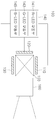
가령, 도 1에 도시된 바와 같이, 종래의 프로젝션 장치는 크게 DLP 방식의 프로젝션 장치와 LCoS 방식의 프로젝션 방식 등이 있다. DLP 방식의 프로젝션 장치는 램프에서 출사된 광원이 여러 색의 컬러휠을 교대로 통과하고, 통과된 광원이 DMD(Digital Micromirror Device) 칩에 반사되어 화면을 표시하는 반사형 소자를 이용하는 방식이다. 이에 반해, LCoS 방식의 프로젝션 방식은 램프에서 출사된 광원이 특수 거울을 통해 분리되고, 상기 분리된 광원이 3개의 LCD 패널(즉, 청색/녹색/적색 LCD 패널)을 각각 투과하여 스크린에 비치도록 하는 방식이다.For example, as shown in FIG. 1, a conventional projection apparatus includes a DLP projection apparatus and an LCoS projection system. In the DLP projection apparatus, a light source emitted from a lamp alternately passes color wheels of various colors, and a light source passed through the DMD (Digital Micromirror Device) chip is used to reflect a screen. In contrast, the LCoS projection system allows the light source emitted from the lamp to be separated through a special mirror, and the separated light source to be transmitted through the three LCD panels (i.e., blue / green / red LCD panels) .
그런데 이러한 DLP 방식 및 LCoS 방식의 프로젝션 장치는, 별도의 광원 램프를 요구하고, 그로 인해 기구 제작의 유연성이 떨어지며, 광 효율이 떨어지는 문제점들이 있다. 따라서, 컴팩트(compact)한 구조를 가지면서 고 해상도의 풀 컬러(full color)를 구현할 수 있는 새로운 프로젝션 장치를 개발할 필요가 있다.However, such DLP-type and LCoS-type projection devices require a separate light source lamp, which results in poor flexibility in the manufacture of the apparatus and low optical efficiency. Therefore, there is a need to develop a new projection device capable of achieving a full color with a high resolution while having a compact structure.
본 발명은 전술한 문제 및 다른 문제를 해결하는 것을 목적으로 한다. 또 다른 목적은 마이크로 LED 패널을 이용한 프로젝션 장치 및 그 제조방법을 제공함에 있다. The present invention is directed to solving the above-mentioned problems and other problems. Another object of the present invention is to provide a projection apparatus using a micro LED panel and a manufacturing method thereof.
또 다른 목적은 청색 마이크로 LED 패널과 색 전환 필름을 이용하여 적색 마이크로 LED 패널을 구현할 수 있는 프로젝션 장치 및 그 제조방법을 제공함에 있다.Another object of the present invention is to provide a projection device capable of realizing a red micro LED panel using a blue micro LED panel and a color conversion film, and a manufacturing method thereof.
또 다른 목적은 녹색 마이크로 LED 패널과 색 전환 필름을 이용하여 적색 마이크로 LED 패널을 구현할 수 있는 프로젝션 장치 및 그 제조방법을 제공함에 있다.Another object of the present invention is to provide a projection device and a method of manufacturing the same that can implement a red micro LED panel using a green micro LED panel and a color conversion film.
또 다른 목적은 사파이어 본딩(Sapphire bonding) 공정을 회피하여 적색 마이크로 LED 패널을 구현할 수 있는 프로젝션 장치 및 그 제조방법을 제공함에 있다.Another object of the present invention is to provide a projection device capable of implementing a red micro LED panel by avoiding a sapphire bonding process and a manufacturing method thereof.
상기 또는 다른 목적을 달성하기 위해 본 발명의 일 측면에 따르면, 제1 파장의 마이크로 LED 픽셀들을 이용하여 제1 파장의 광을 출력하는 제1 마이크로 LED 패널; 제2 파장의 마이크로 LED 픽셀들을 이용하여 제2 파장의 광을 출력하는 제2 마이크로 LED 패널; 상기 제1 또는 제2 파장의 마이크로 LED 픽셀들을 이용하여 제3 파장의 광을 출력하는 제3 마이크로 LED 패널; 및 상기 제1 내지 제3 마이크로 LED 패널에서 출력되는 광들을 합성하는 다이크로익 프리즘(Dichroic Prizm)을 포함하고, 상기 제3 마이크로 LED 패널은, 상기 제1 또는 제2 파장의 광을 상기 제3 파장의 광으로 변환하기 위한 색 변환 필름을 구비하는 것을 특징으로 하는 프로젝션 장치를 제공한다.According to an aspect of the present invention, there is provided a display device comprising: a first micro LED panel that outputs light of a first wavelength using micro LED pixels of a first wavelength; A second micro LED panel for outputting light of a second wavelength using micro LED pixels of a second wavelength; A third micro LED panel for outputting light of a third wavelength using micro LED pixels of the first or second wavelength; And a dichroic prism for synthesizing the lights output from the first through third micro LED panels, wherein the third micro LED panel comprises a light source for emitting the light of the first or second wavelength to the third And a color conversion film for converting the light into a light of a wavelength.
본 발명의 다른 측면에 따르면, 제1 파장의 광을 출력하는 제1 마이크로 LED 디스플레이 장치, 제2 파장의 광을 출력하는 제2 마이크로 LED 디스플레이 장치 및 제3 파장의 광을 출력하는 제3 마이크로 LED 디스플레이 장치를 포함하는 프로젝션 장치에서, GaAs 기판을 형성하는 단계; 상기 GaAs 기판 상에 발광 구조물을 적층하는 단계; 상기 발광 구조물을 단위 픽셀 영역에 따라 에칭 공정을 수행하여 복수의 마이크로 LED 픽셀들을 포함하는 마이크로 LED 패널을 형성하는 단계; 실리콘 기판 상에 상기 마이크로 LED 패널을 플립칩 본딩하는 단계; 및 상기 마이크로 LED 패널에 부착된 GaAs 기판을 분리하는 단계를 포함하는 제3 마이크로 LED 디스플레이 장치의 제조 방법을 제공한다.According to another aspect of the present invention, there is provided a display device including a first micro LED display device for outputting light of a first wavelength, a second micro LED display device for outputting light of a second wavelength, and a third micro LED display device for outputting light of a third wavelength, 1. A projection apparatus comprising a display device, the method comprising: forming a GaAs substrate; Stacking a light emitting structure on the GaAs substrate; Forming a micro LED panel including a plurality of micro LED pixels by etching the light emitting structure along a unit pixel region; Flip-chip bonding the micro LED panel on a silicon substrate; And separating the GaAs substrate attached to the micro LED panel.
본 발명의 실시 예들에 따른 프로젝션 장치 및 그 제조방법의 효과에 대해 설명하면 다음과 같다.Effects of the projection apparatus and the manufacturing method according to the embodiments of the present invention will be described as follows.
본 발명의 실시 예들 중 적어도 하나에 의하면, 적색 마이크로 LED 패널, 녹색 마이크로 LED 패널 및 청색 마이크로 LED 패널을 이용한 프로젝션 장치를 구현함으로써, 컴팩트한 구조를 가질 수 있을 뿐만 아니라 고 해상도(HD 급)의 풀 컬러(full color)를 제공할 수 있다는 장점이 있다.According to at least one of the embodiments of the present invention, by implementing a projection device using a red micro LED panel, a green micro LED panel, and a blue micro LED panel, not only a compact structure but also a high resolution (HD class) The advantage is that it can provide full color.
또한, 본 발명의 실시 예들 중 적어도 하나에 의하면, 청색 마이크로 LED 패널 또는 녹색 마이크로 LED 패널과 색 전환 필름을 이용하여 적색 마이크로 LED 패널을 구현함으로써, 프로젝터에 설치되는 적색 마이크로 LED 패널, 녹색 마이크로 LED 패널 및 청색 마이크로 LED 패널들을 동일한 공정으로 제작할 수 있다는 장점이 있다.In addition, according to at least one embodiment of the present invention, a red micro LED panel is implemented using a blue micro LED panel or a green micro LED panel and a color conversion film, so that a red micro LED panel, a green micro LED panel And blue micro LED panels can be manufactured by the same process.
또한, 본 발명의 실시 예들 중 적어도 하나에 의하면, 사파이어 본딩 공정을 회피하여 적색 마이크로 LED 패널을 구현함으로써, LED 패널 제조 공정을 단순화할 수 있고, 제품 수율을 향상할 수 있으며, 제조 공정 상에 발생하는 성능 저하를 최소화할 수 있다는 장점이 있다.In addition, according to at least one embodiment of the present invention, the red micro LED panel is avoided by avoiding the sapphire bonding process, so that the LED panel manufacturing process can be simplified, the product yield can be improved, The performance degradation can be minimized.
다만, 본 발명의 실시 예들에 따른 프로젝션 장치 및 그 제조방법이 달성할 수 있는 효과는 이상에서 언급한 것들로 제한되지 않으며, 언급하지 않은 또 다른 효과들은 아래의 기재로부터 본 발명이 속하는 기술분야에서 통상의 지식을 가진 자에게 명확하게 이해될 수 있을 것이다.However, the effects that can be achieved by the projection apparatus and the manufacturing method according to the embodiments of the present invention are not limited to those described above, and other effects not mentioned can be obtained from the following description in the technical field It will be understood by those of ordinary skill in the art.
도 1은 종래 프로젝션 장치의 동작 방식을 설명하는 도면;
도 2는 본 발명의 일 실시 예에 따른 프로젝션 장치의 구성도;
도 3은 프로젝션 장치에 구비되는 적색 마이크로 LED 패널, 녹색 마이크로 LED 패널 및 청색 마이크로 LED 패널을 설명하는 도면;
도 4는 데이터 드라이버 IC와 스캔 드라이버 IC를 통해 마이크로 LED 패널을 구동하는 동작을 설명하는 도면;
도 5a는 본 발명의 일 실시 예에 따른 마이크로 LED 패널의 단면도이고, 5 b는 마이크로 LED 디스플레이 장치의 단면도;
도 6a 내지 도 6g는 본 발명의 일 실시 예에 따른 마이크로 LED 디스플레이 장치의 제조방법을 설명하는 도면;
도 7은 본 발명의 다른 실시 예에 따른 프로젝션 장치의 구성도;
도 8은 본 발명의 다른 실시 예에 따른 적색 마이크로 LED 패널을 설명하는 도면;
도 9 및 도 10은 본 발명의 일 실시 예에 따른 퀀텀닷 필름을 설명하는 도면;
도 11은 본 발명의 또 다른 실시 예에 따른 프로젝션 장치의 구성도;
도 12a 내지 도 12e는 본 발명의 일 실시 예에 따른 적색 마이크로 LED 디스플레이 장치의 제조방법을 설명하는 도면;
도 13a 내지 도 13e는 본 발명의 다른 실시 예에 따른 적색 마이크로 LED 디스플레이 장치의 제조방법을 설명하는 도면.1 is a view for explaining an operation method of a conventional projection apparatus;
2 is a configuration diagram of a projection apparatus according to an embodiment of the present invention;
3 is a view illustrating a red micro LED panel, a green micro LED panel, and a blue micro LED panel included in the projection apparatus;
4 is a view for explaining an operation of driving a micro LED panel through a data driver IC and a scan driver IC;
5A is a cross-sectional view of a micro LED panel according to an embodiment of the present invention, and 5B is a sectional view of a micro LED display device.
6A to 6G are views illustrating a method of manufacturing a micro LED display device according to an embodiment of the present invention;
7 is a configuration diagram of a projection apparatus according to another embodiment of the present invention;
8 is a view illustrating a red micro LED panel according to another embodiment of the present invention;
FIGS. 9 and 10 illustrate a quantum dot film according to an embodiment of the present invention;
11 is a configuration diagram of a projection apparatus according to another embodiment of the present invention;
12A to 12E illustrate a method of manufacturing a red micro LED display device according to an embodiment of the present invention;
13A to 13E are views for explaining a manufacturing method of a red micro-LED display device according to another embodiment of the present invention.
이하, 첨부된 도면을 참조하여 본 명세서에 개시된 실시 예를 상세히 설명하되, 도면 부호에 관계없이 동일하거나 유사한 구성요소는 동일한 참조 번호를 부여하고 이에 대한 중복되는 설명은 생략하기로 한다. 이하의 설명에서 사용되는 구성요소에 대한 접미사 "모듈" 및 "부"는 명세서 작성의 용이함만이 고려되어 부여되거나 혼용되는 것으로서, 그 자체로 서로 구별되는 의미 또는 역할을 갖는 것은 아니다. 즉, 본 발명에서 사용되는 '부'라는 용어는 소프트웨어, FPGA 또는 ASIC과 같은 하드웨어 구성요소를 의미하며, '부'는 어떤 역할들을 수행한다. 그렇지만 '부'는 소프트웨어 또는 하드웨어에 한정되는 의미는 아니다. '부'는 어드레싱할 수 있는 저장 매체에 있도록 구성될 수도 있고 하나 또는 그 이상의 프로세서들을 재생시키도록 구성될 수도 있다. 따라서, 일 예로서 '부'는 소프트웨어 구성요소들, 객체지향 소프트웨어 구성요소들, 클래스 구성요소들 및 태스크 구성요소들과 같은 구성요소들과, 프로세스들, 함수들, 속성들, 프로시저들, 서브루틴들, 프로그램 코드의 세그먼트들, 드라이버들, 펌웨어, 마이크로 코드, 회로, 데이터, 데이터베이스, 데이터 구조들, 테이블들, 어레이들 및 변수들을 포함한다. 구성요소들과 '부'들 안에서 제공되는 기능은 더 작은 수의 구성요소들 및 '부'들로 결합되거나 추가적인 구성요소들과 '부'들로 더 분리될 수 있다.Hereinafter, embodiments of the present invention will be described in detail with reference to the accompanying drawings, wherein like reference numerals are used to designate identical or similar elements, and redundant description thereof will be omitted. The suffix "module" and " part "for the components used in the following description are given or mixed in consideration of ease of specification, and do not have their own meaning or role. That is, the term 'part' used in the present invention means a hardware component such as software, FPGA or ASIC, and 'part' performs certain roles. However, 'minus' is not limited to software or hardware. The " part " may be configured to be in an addressable storage medium and configured to play back one or more processors. Thus, by way of example, and by no means, the terms " component " or " component " means any combination of components, such as software components, object- oriented software components, class components and task components, Subroutines, segments of program code, drivers, firmware, microcode, circuitry, data, databases, data structures, tables, arrays and variables. The functions provided in the components and parts may be combined into a smaller number of components and parts or further separated into additional components and parts.
또한, 본 발명에 따른 실시 예의 설명에서, 각 층(막), 영역, 패턴 또는 구조물들이 기판, 각 층(막), 영역, 패드 또는 패턴들의 "상/위(on)"에 또는 "하/아래(under)"에 형성되는 것으로 기재되는 경우에 있어, "상/위(on)"와 "하/아래(under)"는 "직접(directly)" 또는 "다른 층을 개재하여 (indirectly)" 형성되는 것을 모두 포함한다. 또한, 각 층의 상/위 또는 하/아래에 대한 기준은 도면을 기준으로 설명한다. 도면에서 각층의 두께나 크기는 설명의 편의 및 명확성을 위하여 과장되거나 생략되거나 또는 개략적으로 도시되었다. 또한, 각 구성요소의 크기는 실제크기를 전적으로 반영하는 것은 아니다.Also, in the description of the embodiments according to the present invention, it is to be understood that each layer (film), region, pattern or structure may be referred to as being "on" or "under / Quot; under " and " under "are to be understood as being" directly "or" indirectly & . In addition, the criteria for the top / bottom or bottom / bottom of each layer will be described with reference to the drawings. The thickness and size of each layer in the drawings are exaggerated, omitted, or schematically shown for convenience and clarity of explanation. Also, the size of each component does not entirely reflect the actual size.
또한, 본 명세서에 개시된 실시 예를 설명함에 있어서 관련된 공지 기술에 대한 구체적인 설명이 본 명세서에 개시된 실시 예의 요지를 흐릴 수 있다고 판단되는 경우 그 상세한 설명을 생략한다. 또한, 첨부된 도면은 본 명세서에 개시된 실시 예를 쉽게 이해할 수 있도록 하기 위한 것일 뿐, 첨부된 도면에 의해 본 명세서에 개시된 기술적 사상이 제한되지 않으며, 본 발명의 사상 및 기술 범위에 포함되는 모든 변경, 균등물 내지 대체물을 포함하는 것으로 이해되어야 한다.In the following description of the embodiments of the present invention, a detailed description of related arts will be omitted when it is determined that the gist of the embodiments disclosed herein may be blurred. It is to be understood that both the foregoing general description and the following detailed description are exemplary and explanatory and are intended to provide further explanation of the invention as claimed. , ≪ / RTI > equivalents, and alternatives.
본 발명은, 적색 마이크로 LED 패널, 녹색 마이크로 LED 패널 및 청색 마이크로 LED 패널을 이용하여 고 해상도의 풀 컬러(full color)를 구현할 수 있는 프로젝션 장치 및 그 제조방법을 제안한다. The present invention proposes a projection device capable of realizing a full color with high resolution using a red micro LED panel, a green micro LED panel and a blue micro LED panel, and a manufacturing method thereof.
이하에서는, 본 발명의 다양한 실시 예들에 대하여, 도면을 참조하여 상세히 설명한다.Hereinafter, various embodiments of the present invention will be described in detail with reference to the drawings.
도 2는 본 발명의 일 실시 예에 따른 프로젝션 장치의 구성도이다.2 is a configuration diagram of a projection apparatus according to an embodiment of the present invention.
도 2를 참조하면, 본 발명의 일 실시 예에 따른 프로젝션 장치(100)는 적색 마이크로 LED 패널(110), 녹색 마이크로 LED 패널(120), 청색 마이크로 LED 패널(130), LED 구동부(140), 다이크로익 프리즘(150) 및 프로젝션 렌즈(160) 등을 포함할 수 있다. 2, a
적색 마이크로 LED 패널(110)은 웨이퍼(wafer) 상에 적층된 복수의 발광 소자들(즉, 복수의 마이크로 LED 픽셀들)이 매트릭스 형태로 배열된 어레이(array) 구조를 갖는 LED 패널로서, 영상 표시 기기의 영상 신호에 대응하는 적색 광(red light)을 출력하는 기능을 수행할 수 있다. 이때, 해당 패널(110)을 구성하는 복수의 마이크로 LED 픽셀들은 적색 LED 소자로 구성될 수 있다. The red
녹색 마이크로 LED 패널(120)은 웨이퍼(wafer) 상에 적층된 복수의 발광 소자들(즉, 복수의 마이크로 LED 픽셀들)이 매트릭스 형태로 배열된 어레이 구조를 갖는 LED 패널로서, 영상 표시 기기의 영상 신호에 대응하는 녹색 광을 출력하는 기능을 수행할 수 있다. 이때, 해당 패널(120)을 구성하는 복수의 마이크로 LED 픽셀들은 녹색 LED 소자로 구성될 수 있다.The green
청색 마이크로 LED 패널(130)은 웨이퍼(wafer) 상에 적층된 복수의 발광 소자들(즉, 복수의 마이크로 LED 픽셀들)이 매트릭스 형태로 배열된 어레이 구조를 갖는 LED 패널로서, 영상 표시 기기의 영상 신호에 대응하는 청색 광을 출력하는 기능을 수행할 수 있다. 이때, 해당 패널(130)을 구성하는 복수의 마이크로 LED 픽셀들은 청색 LED 소자로 구성될 수 있다.The blue
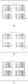
일 예로, 도 3에 도시된 바와 같이, 해당 프로젝션 장치(100)를 구성하는 적색 마이크로 LED 패널(110), 녹색 마이크로 LED 패널(120) 및 청색 마이크로 LED 패널(130)은, 복수의 행(720)과 복수의 열(1280)로 배열된 마이크로 LED 픽셀들을 포함할 수 있다. 또한, 마이크로 LED 패널(110, 120, 130)을 구성하는 복수의 마이크로 LED 픽셀들의 크기는 각각 8㎛ * 8㎛의 크기로 구성될 수 있다. 하지만, 프로젝션 장치(100)의 용도 및 종류 등에 따라, 마이크로 LED 패널(110, 120, 130)의 픽셀 수 및 크기 등을 변경하여 제작할 수 있음은 당업자에게 자명할 것이다.3, the red
해당 프로젝션 장치(100)를 구성하는 적색 마이크로 LED 패널(110), 녹색 마이크로 LED 패널(120) 및 청색 마이크로 LED 패널(130)들은 서로 인접하는 패널에 대해 수직 방향이 되도록 배치될 수 있다. 일 예로, 다이크로익 프리즘(150)의 좌측 영역에 녹색 마이크로 LED 패널(120)을 배치하고, 다이크로익 프리즘(150)의 상부 영역에 적색 마이크로 LED 패널(110)을 배치하며, 다이크로익 프리즘(150)의 하부 영역에 청색 마이크로 LED 패널(130)을 배치할 수 있다.The red
LED 구동부(140)는 적색 마이크로 LED 패널(110), 녹색 마이크로 LED 패널(120) 및 청색 마이크로 LED 패널(130)을 구동하는 동작을 수행할 수 있다. 즉, LED 구동부(140)는 적색 마이크로 LED 패널(110)을 구동하기 위한 R-LED 구동부(141), 녹색 마이크로 LED 패널(120)을 구동하기 위한 G-LED 구동부(143) 및 청색 마이크로 LED 패널(130)을 구동하기 위한 B-LED 구동부(145)를 포함할 수 있다.The
한편, 본 실시 예에서는, 설명의 편의상, R-LED 구동부(141), G-LED 구동부(143) 및 B-LED 구동부(145)가 독립적으로 구성되는 예를 도시하고 있으나 이에 제한되지는 않으며, 상기 적색 마이크로 LED 패널(110), 녹색 마이크로 LED 패널(120) 및 청색 마이크로 LED 패널(130)과 일체로 형성될 수 있음은 당업자에게 자명할 것이다. 즉, R-LED 구동부(141), G-LED 구동부(143) 및 B-LED 구동부(145)은, 적색 마이크로 LED 패널(110), 녹색 마이크로 LED 패널(120) 및 청색 마이크로 LED 패널(130)의 뒤쪽 방향에 배치되는 CMOS 백플레인(backplane)으로 구성될 수 있다.In the present embodiment, the R-LED driver 141, the G-
CMOS 백플레인은 복수의 마이크로 LED 픽셀들을 개별 구동시키기 위한 복수의 CMOS 셀들을 구비하는 Active Matrix 회로부와, 상기 Active Matrix 회로부의 외곽에 배치되는 공통 셀을 포함할 수 있다.The CMOS backplane may include an active matrix circuit portion having a plurality of CMOS cells for individually driving a plurality of micro LED pixels, and a common cell disposed outside the active matrix circuit portion.
Active Matrix 회로부에 구비되는 복수의 CMOS 셀들 각각은 범프를 통해 대응되는 마이크로 LED 픽셀에 전기적으로 연결된다. 복수의 CMOS 셀들 각각은 대응되는 마이크로 LED 픽셀을 개별적으로 구동시키기 위한 집적회로(IC)이다. 따라서, 복수의 CMOS 셀들 각각은, 두 개의 트랜지스터와 하나의 커패시터를 포함하는 픽셀 구동 회로일 수 있고, 범프들을 이용하여 CMOS 백플레인에 마이크로 LED 패널을 플립칩 본딩하는 경우, 등가 회로상, 상기 픽셀 구동 회로의 트랜지스터의 드레인 단자와 공통 접지 단자 사이에 개개의 마이크로 LED 픽셀이 배치되는 형태로 구성될 수 있다.Each of the plurality of CMOS cells provided in the active matrix circuit portion is electrically connected to corresponding micro LED pixels through bumps. Each of the plurality of CMOS cells is an integrated circuit (IC) for individually driving corresponding micro LED pixels. Thus, each of the plurality of CMOS cells may be a pixel driving circuit including two transistors and one capacitor, and when flip chip bonding the micro LED panel to the CMOS backplane using bumps, on the equivalent circuit, And the individual micro LED pixels are disposed between the drain terminal of the transistor of the circuit and the common ground terminal.
Active Matrix 회로부의 외곽에 배치되는 공통 셀은 데이터 드라이버 IC(data driver IC)와 스캔 드라이버 IC(scan driver IC)를 포함할 수 있다. 가령, 도 4에 도시된 바와 같이, 마이크로 LED 패널(110~130)을 구성하는 복수의 마이크로 LED 픽셀들(미도시)은 복수의 스캐닝 라인(425)과 복수의 데이터 라인(415)의 교차 지점들에 위치할 수 있다. 복수의 마이크로 LED 픽셀들로 입력되는 복수의 스캐닝 라인(425)은 스캔 드라이버 IC(420)에 의해 제어되고, 복수의 데이터 라인(415)은 데이터 드라이버 IC(410)에 의해 제어된다.The common cell disposed outside the active matrix circuit part may include a data driver IC (data driver IC) and a scan driver IC (scan driver IC). 4, a plurality of micro LED pixels (not shown) constituting the
이러한 CMOS 백플레인을 통한 마이크로 LED 패널(110~130)의 제어 동작을 간단히 살펴보면, 스캔 드라이버 IC(420)는, 이미지 데이터 제공 시, 복수의 스캐닝 라인(425) 모두를 스캐닝하면서 그 중 어느 하나 이상에 H(high) 신호를 입력하여 턴 온(turn on) 시킨다. 한편, 데이터 드라이버 IC(410)에서 이미지 데이터를 복수의 데이터 라인들(415)로 공급하면, 상기 스캐닝 라인에서 턴 온 상태에 놓인 픽셀들이 상기 이미지 데이터들을 통과시켜 해당 이미지 데이터가 마이크로 LED 패널을 통해 표시되도록 한다. 이러한 방식으로 모든 스캐닝 라인이 순차적으로 스캐닝되면서 한 프레임(frame)에 대한 디스플레이가 완료된다.The control operation of the
다이크로익 프리즘(Dichroic Prizm, 150)은 적색 마이크로 LED 패널(110)로부터 출력되는 적색 광과, 녹색 마이크로 LED 패널(120)로부터 출력되는 녹색 광과, 청색 마이크로 LED 패널(130)로부터 출력되는 청색 광을 합성하는 기능을 수행할 수 있다.The
프로젝션 렌즈(160)는 다이크로익 프리즘(Dichroic Prizm, 150)으로부터 출력되는 합성 광을 확대하여 전방의 스크린으로 방사하는 기능을 수행할 수 있다.The
이상 상술한 바와 같이, 적색 마이크로 LED 패널, 녹색 마이크로 LED 패널 및 청색 마이크로 LED 패널을 이용한 프로젝션 장치(100)는 별도의 광원 램프를 요구하지 않으므로 기구 제작의 유연성을 향상시킬 수 있고, 광 효율 및 색 재현성의 증가로 인해 고 해상도의 풀 컬러(full color)를 구현할 수 있다.As described above, since the
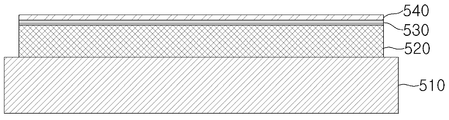
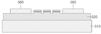
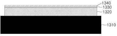
도 5a는 본 발명의 일 실시 예에 따른 마이크로 LED 패널의 단면도이고, 도 5 b는 마이크로 LED 디스플레이 장치의 단면도다. 여기서, 마이크로 LED 디스플레이 장치는 마이크로 LED 패널과 CMOS 백플레인을 범프를 통해 플립칩 본딩함으로써 형성될 수 있다. 5A is a cross-sectional view of a micro LED panel according to an embodiment of the present invention, and FIG. 5B is a cross-sectional view of a micro LED display device. Here, the micro LED display device can be formed by flip-chip bonding the micro LED panel and the CMOS backplane through the bumps.
도 5a를 참조하면, 본 발명에 따른 마이크로 LED 패널(500)은, 웨이퍼 상에 적층된 복수의 발광 소자들(즉, 복수의 마이크로 픽셀들)이 매트릭스 형태로 배열되는 어레이 구조를 갖는 LED 패널로서, 영상 표시 기기의 영상 신호에 대응하는 광(light)을 출력하는 기능을 수행할 수 있다.5A, a
이러한 마이크로 LED 패널(500)은 기판(510), 상기 기판(510) 상에 제1 도전형 반도체층(520), 상기 제1 도전형 반도체층(520) 상에 활성층(530), 상기 활성층(530) 상에 제2 도전형 반도체층(540), 제1 및 2 도전형 메탈층(550, 560), 패시베이션 층(570) 등을 포함할 수 있다.The
기판(510)은 투광성을 갖는 재질, 예를 들어, 사파이어(Al2O3), 단 결정 기판, SiC, GaAs, GaN, ZnO, AlN, Si, GaP, InP, Ge 중 적어도 하나로 형성될 수 있으며, 이에 대해 한정하지는 않는다. The
제1 도전형 반도체층(520)은 n형 도펀트가 도핑된 족-족 원소의 화합물 반도체를 포함할 수 있다. 이러한 제1 도전형 반도체층(520)은 InxAlyGa1 -x- yN (0≤x≤1, 0≤y≤1, 0≤x+y≤1)의 조성식을 갖는 반도체 재료, 예를 들어 InAlGaN, GaN, AlGaN, AlInN, InGaN, AlN, InN 등에서 선택될 수 있으며, Si, Ge, Sn 등의 n형 도펀트가 도핑될 수 있다.The first
활성층(530)은 제1 도전형 반도체층(520)을 통해서 주입되는 전자(또는 정공)와 제2 도전형 반도체층(540)을 통해서 주입되는 정공(또는 전자)이 서로 만나서, 활성층(430)의 형성 물질에 따른 에너지 밴드(Energy Band)의 밴드갭(Band Gap) 차이에 의해서 빛을 방출하는 층이다. 상기 활성층(530)은 단일 양자 우물 구조, 다중 양자 우물 구조(MQW: Multi Quantum Well), 양자점 구조 또는 양자선 구조 중 어느 하나로 형성될 수 있으나, 이에 한정되는 것은 아니다. 상기 활성층(530)은 InxAlyGa1 -x- yN (0≤x≤1, 0≤y≤1, 0≤x+y≤1)의 조성식을 갖는 반도체 재료로 형성될 수 있다. 활성층(530)이 다중 양자 우물 구조로 형성된 경우, 상기 활성층(530)은 복수의 우물층과 복수의 장벽층이 교대로 적층되어 형성될 수 있다.The
제2 도전형 반도체층(540)은 p형 도펀트가 도핑된 족-족 원소의 화합물 반도체를 포함할 수 있다. 이러한 제2 도전형 반도체층(540)은 InxAlyGa1 -x- yN (0≤x≤1, 0≤y=1, 0≤x+y≤1)의 조성식을 갖는 반도체 재료, 예를 들어 InAlGaN, GaN, AlGaN, InGaN, AlInN, AlN, InN 등에서 선택될 수 있으며, Mg, Zn, Ca, Sr, Ba 등의 p형 도펀트가 도핑될 수 있다.The second
제2 도전형 반도체층(540) 상에는 제2 도전형 메탈층(즉, p 전극, 550)이 형성될 수 있고, 상기 제1 도전형 반도체층(520) 상에는 제1 도전형 메탈층(즉, n 전극, 560)이 형성될 수 있다. 상기 제1 및 제2 도전형 메탈층(550, 560)은 마이크로 LED 패널(500)에 형성된 복수의 마이크로 LED 픽셀들로 전원을 제공한다.A second conductive type metal layer (i.e., a p-electrode) 550 may be formed on the second conductive
제2 도전형 메탈층(550)은 각각의 마이크로 LED 픽셀에 대응하는 제2 도전형 반도체층(540) 상에 배치되며, CMOS 백플레인(600)에 구비된 각각의 CMOS 셀(620)과 범프(650)를 통해 전기적으로 연결될 수 있다. 한편, 다른 실시 예로, 제2 도전형 반도체층(540) 상에 DBR(Distributed Bragg Reflector) 등과 같은 반사층(미도시)이 존재하는 경우, 상기 제2 도전형 메탈층(550)은 반사층 상에 배치될 수 있다.The second
제1 도전형 메탈층(560)은 제1 도전형 반도체층(520)의 메사 식각된 영역 상에 배치되며, 상기 복수의 마이크로 LED 픽셀들과 일정 거리만큼 이격되도록 형성될 수 있다. 제1 도전형 메탈층(560)은 제1 도전형 반도체층(520) 상에서 마이크로 LED 패널(500)의 외곽을 따라 소정의 폭을 갖도록 형성될 수 있다. 제1 도전형 메탈층(560)의 높이는 상기 복수의 마이크로 LED 픽셀들의 높이와 대체로 동일하게 형성될 수 있다. 제1 도전형 메탈층(560)은 범프에 의해 CMOS 백플레인(600)의 공통 셀(610)과 전기적으로 연결되어, 마이크로 LED 픽셀들의 공통 전극으로서 기능한다. 예를 들어, 제1 도전형 메탈층(560)은 공통 접지일 수 있다.The first
제1 도전형 반도체층(520), 활성층(530), 제2 도전형 반도체층(540), 제2 도전형 메탈층(550) 및 제1 도전형 메탈층(560)의 적어도 일 측면에는 패시베이션층(570)이 형성될 수 있다. 상기 패시베이션층(570)은 발광 구조물(520, 530, 540)을 전기적으로 보호하기 위하여 형성될 수 있으며, 예를 들어, SiO2, SiOx, SiOxNy, Si3N4, Al2O3 로 형성될 수 있으나, 이에 대해 한정하지는 않는다.At least one side of the first conductive
이와 같이 형성된 발광 소자들(즉, 복수의 마이크로 LED 픽셀들)은 화합물 반도체의 조성비에 따라 서로 다른 파장의 광을 방사할 수 있다. 마이크로 LED 패널(500)에 포함된 발광 소자들이 적색 LED 소자인 경우, 상기 마이크로 LED 패널(500)은 적색 마이크로 LED 패널(500)일 수 있다. 마이크로 LED 패널(500)에 포함된 발광 소자들이 녹색 LED 소자인 경우, 상기 마이크로 LED 패널(500)은 녹색 마이크로 LED 패널(500)일 수 있다. 마이크로 LED 패널(500)에 포함된 발광 소자들이 청색 LED 소자인 경우, 상기 마이크로 LED 패널(500)은 청색 마이크로 LED 패널(500)일 수 있다.The light emitting devices thus formed (i.e., the plurality of micro LED pixels) may emit light of different wavelengths depending on the composition ratio of the compound semiconductor. When the light emitting elements included in the
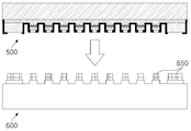
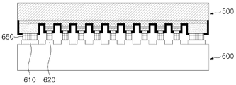
도 5b를 참조하면, 마이크로 LED 디스플레이 장치는 마이크로 LED 패널(500), CMOS 백플레인(600), 및 범프들(650)을 포함한다. 이때, CMOS 백플레인(600)은 복수 개의 CMOS 셀들(620)을 포함하는 Active Matrix 회로부와, 상기 Active Matrix 회로부의 외곽에 배치되는 공통 셀(610)을 포함할 수 있다. Referring to FIG. 5B, the micro LED display device includes a
마이크로 LED 패널(500)은 복수의 마이크로 LED 픽셀들을 포함하고, CMOS 백플레인(600)은, 복수의 마이크로 LED 픽셀들 각각을 개별 구동시키기 위해 마이크로 LED 픽셀들 각각에 대응하는 복수 개의 CMOS 셀들(620)을 포함한다. 이때, 마이크로 LED 패널(500)의 픽셀 영역은 CMOS 백플레인(600)의 AM 영역과 대응될 수 있다. The
범프들(650)은, 마이크로 LED 픽셀들과 CMOS 셀들(650)이 마주하도록 배치된 상태에서, 마이크로 LED 픽셀들 각각과 이들 각각에 대응하는 CMOS 셀들(610)이 전기적으로 연결되도록 한다.The
이러한 마이크로 LED 디스플레이 장치의 제조 공정을 간단히 살펴보면, 먼저 복수의 범프들(650)을 CMOS 백플레인(600)의 CMOS 셀들(620)과 공통 셀(610)의 상부에 배치한다. 그리고, 상기 복수의 범프들(650)이 배치된 상태의 CMOS 백플레인(600)과 마이크로 LED 패널(500)을 서로 마주보게 하여 CMOS 셀들(620)과 마이크로 LED 픽셀들을 일대일 대응시켜 밀착시킨 후 가열한다. 그러면, 상기 복수의 범프들(650)이 녹게 되고, 그에 따라 CMOS 셀들(620)과 그에 대응하는 마이크로 LED 픽셀들이 전기적으로 연결되고, 공통 셀(610)과 그에 대응하는 마이크로 LED 패널(500)의 공통 전극(560)이 전기적으로 연결되는 상태가 된다. First, a plurality of
도 6a 내지 도 6g는 본 발명의 일 실시 예에 따른 마이크로 LED 디스플레이 장치의 제조방법을 설명하는 도면이다.6A to 6G are views illustrating a method of manufacturing a micro LED display device according to an embodiment of the present invention.
도 6a를 참조하면, 기판(510) 상에 제1 도전형 반도체층(520), 활성층(530) 및 제2 도전형 반도체층(540)을 순차적으로 성장하여 발광 구조물(520, 530, 540)을 형성할 수 있다.Referring to FIG. 6A, a first
기판(510)은 투광성을 갖는 재질, 예를 들어, 사파이어(Al2O3), 단 결정 기판, SiC, GaAs, GaN, ZnO, AlN, Si, GaP, InP, Ge 중 적어도 하나로 형성될 수 있으며, 이를 한정하지는 않는다.The
제1 도전형 반도체층(520)은 InxAlyGa1 -x- yN (0≤x≤1, 0≤y≤1, 0≤x+y≤1)의 조성식을 갖는 반도체 재료, 예를 들어 InAlGaN, GaN, AlGaN, AlInN, InGaN, AlN, InN 등에서 선택될 수 있으며, Si, Ge, Sn 등의 n형 도펀트가 도핑될 수 있다. 이러한 제1 도전형 반도체층(520)은 트리메틸 갈륨(TMGa) 가스, 암모니아(NH3) 가스, 사일렌(SiH4) 가스를 수소 가스와 함께 챔버(chamber)에 주입하여 형성될 수 있다. 기판(510)과 제1 도전형 반도체층(520) 사이에 언도프트 반도체층(미도시) 및/또는 버퍼층(미도시)을 더 포함할 수 있으며, 이에 대해 한정하지는 않는다.The first
활성층(530)은 InxAlyGa1 -x- yN (0≤x≤1, 0≤y≤1, 0≤x+y≤1)의 조성식을 갖는 반도체 재료로 형성될 수 있다. 이러한 활성층(530)은 트리메틸 갈륨(TMGa) 가스, 트리메틸 인듐(TMIn) 가스, 암모니아(NH3) 가스를 수소 가스와 함께 챔버에 주입하여 형성될 수 있다.The
제2 도전형 반도체층(540)은 InxAlyGa1 -x- yN (0≤x≤1, 0≤y≤1, 0≤x+y≤1)의 조성식을 갖는 반도체 재료, 예를 들어 InAlGaN, GaN, AlGaN, InGaN, AlInN, AlN, InN 등에서 선택될 수 있으며, Mg, Zn, Ca, Sr, Ba 등의 p형 도펀트가 도핑될 수 있다. 이러한 제2 도전형 반도체층(540)은 트리메틸 갈륨(TMGa) 가스, 암모니아(NH3) 가스, 비세틸 사이클로 펜타디에닐 마그네슘(EtCp2Mg){Mg(C2H5C5H4)2} 가스를 수소 가스와 함께 챔버에 주입하여 형성될 수 있다. The second conductivity
도 6b를 참조하면, 발광 구조물(520, 530, 540)을 단위 픽셀 영역에 따라 아이솔레이션 에칭(isolation etching) 공정을 수행하여 복수 개의 발광 소자들을 형성할 수 있다. 예를 들어, 상기 아이솔레이션 에칭은 ICP(Inductively Coupled Plasma)와 같은 건식 식각 방법에 의해 실시될 수 있다. 이러한 아이솔레이션 에칭 공정을 통해 제1 도전형 반도체층(520)의 일 상면이 노출된다. 이때, 공통 전극(즉, n 전극, 560)을 형성하기 위해, 제1 도전형 반도체층(520)의 테두리 영역이 소정의 폭을 갖도록 식각될 수 있다.Referring to FIG. 6B, a plurality of light emitting devices may be formed by performing an isolation etching process on the
도 6c 및 도 6d를 참조하면, 제2 도전형 반도체층(540)의 일 상면에 제2 도전형 메탈층(550)을 형성할 수 있고, 메사 식각된 제1 도전형 반도체층(520)의 일 상면에 제1 도전형 메탈층(560)을 형성할 수 있다. 이때, 상기 제1, 2 도전형 메탈층(550, 560)은 증착 공정 또는 도금 공정에 의해 형성될 수 있으며, 이에 대해 한정하지는 않는다.Referring to FIGS. 6C and 6D, a second conductive
도 6e를 참조하면, 기판(510), 발광 구조물(520, 530, 540), 제2 도전형 메탈층(550) 및 제1 도전형 메탈층(560) 상에 패시베이션층(570)을 형성하고, 상기 제1 및 제2 도전형 메탈층(550, 560)의 일 상면이 외부로 노출되도록 상기 패시베이션층(570)을 선택적으로 제거할 수 있다.6E, a
도 6f 및 도 6g를 참조하면, CMOS 백플레인(600)의 CMOS 셀들(620)과 공통 셀(610)의 상부에 복수의 범프들(650)을 배치한다. 마이크로 LED 패널(500)을 상/하로 반전하여 제1 및 제2 도전형 메탈층(550, 560)이 아래 방향을 향하도록 한다. 상기 복수의 범프들(650)이 배치된 상태의 CMOS 백플레인(600)과 마이크로 LED 패널(500)을 서로 마주보게 하여 CMOS 셀들(620)과 마이크로 LED 픽셀들을 일대일 대응시켜 밀착시킨 후 가열한다. 그러면, 상기 복수의 범프들(630)이 녹게 되고, 그에 따라 CMOS 셀들(620)과 그에 대응하는 마이크로 LED 픽셀들이 전기적으로 연결되고, CMOS 백플레인(600)의 공통 셀(610)과 그에 대응하는 마이크로 LED 패널(500)의 공통 전극(560)이 전기적으로 연결되는 상태가 된다. 이처럼, 복수의 범프(650)를 통해 CMOS 백플레인(600)과 마이크로 LED 패널(500)을 플립칩 본딩하여 마이크로 LED 디스플레이 장치를 형성할 수 있다.Referring to FIGS. 6F and 6G, a plurality of
도 7은 본 발명의 다른 실시 예에 따른 프로젝션 장치의 구성도이다.7 is a configuration diagram of a projection apparatus according to another embodiment of the present invention.
도 7을 참조하면, 본 발명의 다른 실시 예에 따른 프로젝션 장치(700)는 적색 마이크로 LED 패널(710), 녹색 마이크로 LED 패널(720), 청색 마이크로 LED 패널(730), LED 구동부(740), 다이크로익 프리즘(750) 및 프로젝션 렌즈(760) 등을 포함할 수 있다. 여기서, 적색 마이크로 LED 패널(710)을 제외한 나머지 구성 요소들은, 도 2에 도시된 구성 요소들과 동일하다. 따라서, 도 7에 도시된 녹색 마이크로 LED 패널(720), 청색 마이크로 LED 패널(730), LED 구동부(740), 다이크로익 프리즘(750) 및 프로젝션 렌즈(760)에 대한 자세한 설명은 생략하도록 한다.7, a
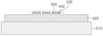
도 2의 프로젝션 장치(100)와 달리, 해당 프로젝션 장치(700)를 구성하는 적색 마이크로 LED 패널(710)은, 청색 마이크로 LED 패널(711)과 색 전환 필름(713)으로 구성될 수 있다.Unlike the
통상, 청색 LED 소자 및 녹색 LED 소자는 사파이어 기판 상에서 성장되고 적색 LED 소자는 GaAs 기판 상에서 성장되므로, 녹색 마이크로 LED 패널 및 청색 마이크로 LED 패널은 동일 공정에서 제작 가능하나, 적색 마이크로 LED 패널은 GaAs 기판을 분리하기 위한 추가 공정이 필요하다. 따라서, 청색 마이크로 LED 패널(711)과 색 전환 필름(713)으로 적색 마이크로 LED 패널(710)을 구현한다면, 동일한 공정을 사용하여 프로젝션 장치(700)의 모든 마이크로 LED 패널들(710, 720, 730)을 제작할 수 있다.Since a blue LED device and a green LED device are grown on a sapphire substrate and a red LED device is grown on a GaAs substrate, a green micro LED panel and a blue micro LED panel can be manufactured in the same process, An additional process for separation is needed. Therefore, if the red
도 8은 본 발명의 다른 실시 예에 따른 적색 마이크로 LED 패널을 설명하는 도면이다.8 is a view illustrating a red micro LED panel according to another embodiment of the present invention.
도 8을 참조하면, 본 발명에 따른 적색 마이크로 LED 패널(710)은 청색 마이크로 LED 패널(711)과 상기 청색 마이크로 LED 패널(711) 상의 색 전환 필름(713)을 포함할 수 있다. Referring to FIG. 8, the red
적색 마이크로 LED 패널(710)을 구성하는 청색 마이크로 LED 패널(711)은, 복수의 마이크로 LED 픽셀들이 매트릭스 형태로 배열된 어레이 구조를 갖는 패널로서, 영상 표시 기기의 영상 신호에 대응하는 청색 광을 출력하는 기능을 수행할 수 있다. 이때, 해당 패널(711)을 구성하는 복수의 마이크로 LED 픽셀들은 청색 LED 소자로 구성될 수 있다.The blue
색 전환 필름(713)은 청색 마이크로 LED 패널(711)에서 방사되는 청색 광을 적색 광으로 변환하는 기능을 수행할 수 있다. 통상, 색 전환 필름(713)은 접착제 또는 접착 성분을 포함하고 있어, 청색 광이 방사되는 청색 마이크로 LED 패널(711)의 일 면에 부착될 수 있다. 한편, 다른 실시 예로, 접착제 또는 접착 성분이 색 전환 필름(713)에 포함되지 않은 경우, 청색 마이크로 LED 패널(711)과 색 전환 필름(713) 사이에는 별도의 접착층(adhesive lay) 또는 접착 시트(adhesive sheet)가 형성될 수 있다.The
이러한 색 전환 필름(713)의 일 예로 형광체 필름, 퀀텀닷 필름(Quantum Dots film)이 사용될 수 있으며, 이에 한정되지는 않는다.As an example of such a
한편, 이상 본 실시 예에서는, 청색 마이크로 LED 패널과 색 전환 필름을 이용하여 적색 마이크로 LED 패널을 구현하는 것을 예시하고 있으나 이를 제한하지는 않으며, 녹색 마이크로 LED 패널과 색 전환 필름을 이용하여 적색 마이크로 LED 패널을 구현할 수 있음은 당업자에게 자명할 것이다.In the present embodiment, the red micro LED panel is implemented using the blue micro LED panel and the color conversion film. However, the present invention is not limited thereto, It will be apparent to those skilled in the art.
또한, 이상 본 실시 예에서는, 상기 적색 마이크로 LED 패널(710)이 피코 프로젝터(700)에 적용되는 것을 예시하고 있으나 이를 제한하지는 않으며, 차량용 헤드업 디스플레이(Head-Up Display, HUD) 또는 헤드 마운티드 디스플레이(Head Mounted Display, HMD) 등과 같은 다양한 표시 장치에 적용될 수 있음은 당업자에게 자명할 것이다.In the present embodiment, the red
도 9 및 도 10은 본 발명의 일 실시 예에 따른 퀀텀닷 필름을 설명하는 도면이다.9 and 10 are views illustrating a quantum dot film according to an embodiment of the present invention.
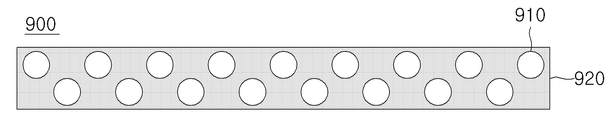
도 9를 참조하면, 본 발명에 따른 퀀텀닷 필름(900)은 복수의 퀀텀닷(910)이 분산되어 있는 고분자층(920)을 포함할 수 있다.Referring to FIG. 9, the
고분자층(920)은 플라스틱 레진(plastic resin)으로 형성될 수 있다. 플라스틱 레진은 폴리머 또는 실리콘 계열의 필름을 형성하는 다양한 물질을 포함할 수 있으며, 물질의 종류는 한정되지 않는다. 본 발명의 실시 예에서, 플라스틱 레진에 필요한 특성은 경화된 상태에서 빛을 투과시키는 특성을 가지면 충분하며, 빛의 투과율에 대한 제한은 없다.The
고분자층(920)에는 빛의 파장을 변화시켜 색 재현성 및 색 순도를 구현할 수 있는 퀀텀닷(910)이 분산되어 있다. 퀀텀닷(또는 양자점, Quantum Dot, 910)은 지름이 수 나노미터(nm)인 반도체 나노 입자로 양자구속 혹은 양자가둠 효과(Quantum Confinement Effect)와 같은 양자 역학(Quantum Mechanics)적 특성을 지니고 있다. 여기서, 양자구속 효과란 반도체 나노 입자의 크기가 작아짐에 따라 띠 간격 에너지(band gap energy)가 커지는(역으로 파장은 작아지는) 현상을 의미한다.
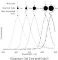
이와 같은 퀀텀닷(910)의 대표적 특성은, 빛이 닿으면 발광(Photo Luminescence, PL)하거나 전기를 흘리면 발광(Electron Luminescence, EL)하는 것이다. 화학 합성 공정으로 만들어지는 퀀텀닷(910)은 재료를 바꾸지 않고 입자 크기를 조절하는 것 만으로도 원하는 색상을 구현할 수 있다. 가령, 도 10에 도시된 바와 같이, 양자구속 효과에 따라 나노 입자 크기가 작을수록 짧은 파장을 갖는 청색 빛을 발광할 수 있고, 나노 입자의 크기가 클수록 긴 파장을 갖는 적색 빛을 발광할 수 있다.A typical characteristic of the
고분자층(920)에 분산되어 있는 퀀텀닷(910)의 직경은 1nm 내지 10nm의 범위일 수 있다. 본 발명의 실시 예에 따른 컨텀닷(910)은, 청색 광을 적색 광으로 변환하기 위해, 5nm 내지 7nm의 직경을 가질 수 있다. 좀 더 바람직하게는, 퀀텀닷(910)은 6nm의 직경을 가질 수 있다. The diameter of the
퀀텀닷(910)은 Ⅱ-Ⅵ족, Ⅲ-Ⅴ족 또는 Ⅳ족 물질일 수 있으며, 구체적으로 CdSe, CdTe, CdS, ZnSe, ZnTe, ZnS, InP, GaP, GaInP2, PbS, ZnO, TiO2, AgI, AgBr, Hg12, PbSe, In2S3, In2Se3, Cd3P2, Cd3As2 또는 GaAs일 수 있다.The
또한, 퀀텀닷(910)은 코어-쉘 구조(core-shell)를 가질 수 있다. 여기서, 코어(core)는 CdSe, CdTe, CdS, ZnSe, ZnTe, ZnS, HgTe 및 HgS 으로 이루어지는 그룹에서 선택된 어느 하나의 물질을 포함하고, 쉘(shell)은 CdSe, CdTe, CdS, ZnSe, ZnTe, ZnS, HgTe 및 HgS 으로 이루어지는 그룹에서 선택된 어느 하나의 물질을 포함할 수 있다.In addition,
한편, 도면에 도시되고 있지 않지만, 상기 퀀텀닷 필름(900)은 고분자층(920)의 적어도 일 면에 부착되는 베리어 층(미도시)을 추가로 포함할 수 있다.Although not shown in the figure, the
도 11은 본 발명의 또 다른 실시 예에 따른 프로젝션 장치의 구성도이다.11 is a configuration diagram of a projection apparatus according to another embodiment of the present invention.
도 11을 참조하면, 본 발명의 또 다른 실시 예에 따른 프로젝션 장치(1100)는 적색 마이크로 LED 패널(1110), 녹색 마이크로 LED 패널(1120), 청색 마이크로 LED 패널(1130), LED 구동부(1140), 다이크로익 프리즘(1150) 및 프로젝션 렌즈(1160) 등을 포함할 수 있다. 여기서, 적색 마이크로 LED 패널(1110)을 제외한 나머지 구성 요소들은, 도 2에 도시된 구성 요소들과 동일하다. 따라서, 도 11에 도시된 녹색 마이크로 LED 패널(1120), 청색 마이크로 LED 패널(1130), LED 구동부(1140), 다이크로익 프리즘(1150) 및 프로젝션 렌즈(1160)에 대한 자세한 설명은 생략하도록 한다.11, a
도 2의 프로젝션 장치(100)와 달리, 해당 프로젝션 장치(1100)를 구성하는 적색 마이크로 LED 패널(1110)은, 사파이어 본딩(Sapphire Bonding) 회피 공정을 통해 제조될 수 있다. 이하에서는, 사파이어 본딩 공정을 이용한 적색 마이크로 LED 패널 제조 방법과 사파이어 본딩 공정을 회피한 적색 마이크로 LED 패널 제조 방법을 구분하여 설명하도록 한다.Unlike the
도 12a 내지 도 12g는 본 발명의 일 실시 예에 따른 적색 마이크로 LED 디스플레이 장치의 제조방법을 설명하는 도면이다.12A to 12G are views illustrating a method of manufacturing a red micro LED display device according to an embodiment of the present invention.
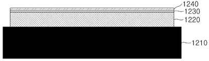
도 12a를 참조하면, GaAs 기판(1210) 상에 제1 도전형 반도체층(1220), 활성층(1230) 및 제2 도전형 반도체층(1240)을 순차적으로 성장하여 발광 구조물(1220, 1230, 1240)을 형성할 수 있다. 여기서, 사파이어 기판 대신, GaAs 기판을 사용하는 이유는, 적색 광을 방사하는 발광 구조물(1220, 1230, 1240)과 유사한 격자 상수(lattice Constant)를 가지고 있기 때문이다. 따라서, GaAs 기판(1210) 위에 발광 구조물(1220, 1230, 1240)을 적층하는 경우, 격자 상수 차이에 의한 스트레인(strain)이 발생하지 않게 된다.12A, a first conductivity
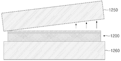
도 12b를 참조하면, 제2 도전형 반도체층(1240)의 상면에 제1 사파이어 기판(1250)을 결합할 수 있다. 이때, 제2 도전형 반도체층(1240)과 제1 사파이어 기판(1250) 사이는 접착층 또는 접착제를 통해 결합될 수 있다. 여기서, 제1 사파이어 기판(1250)은 GaAs 기판(1210)을 제거하기 위한 지지층 역할을 수행할 수 있다.Referring to FIG. 12B, the
도 12c를 참조하면, 레이저 리프트 오프(laser lift off, LLO), 화학적 리프트 오프(chemical lift off, CLO), 전기적 리프트 오프(electrical lift off, ELO) 또는 식각 방법 등을 사용하여 제1 도전형 반도체층(1220)의 하면에 부착된 GaAs 기판(1210)을 분리할 수 있다. 여기서, GaAs 기판(1210)를 분리하는 이유는, GaAs 기판(1210)이 발광 구조물(1220, 1230, 1240)에서 방사되는 적색 파장을 흡수하는 성질을 가지고 있기 때문이다. 따라서, 발광 구조물(1220, 1230, 1240)을 성장시킨 후, GaAs 기판(1210)을 사파이어 기판으로 교체할 필요가 있다. 이때, 사파이어 기판을 사용하는 이유는, 다른 기판에 비해 빛 투과성이 우수하고, 가격 경쟁력이 우수하기 때문이다. Referring to FIG. 12C, a first conductivity type semiconductor is formed using a laser lift off (LLO), a chemical lift off (CLO), an electrical lift off (ELO) The
도 12d를 참조하면, 제1 도전형 반도체층(1220)의 하면에 제2 사파이어 기판(1260)을 결합할 수 있다. 이때, 제1 도전형 반도체층(1220)과 제2 사파이어 기판(1260) 사이는 접착층 또는 접착제를 통해 결합될 수 있다. 여기서, 제2 사파이어 기판(1260)은 발광 구조물(1220, 1230, 1240)의 상/하 위치를 바꾸는 역할을 수행하기 위한 것이다.Referring to FIG. 12D, a
도 12e를 참조하면, 레이저 리프트 오프(laser lift off, LLO), 화학적 리프트 오프(chemical lift off, CLO), 전기적 리프트 오프(electrical lift off, ELO) 또는 식각 방법 등을 사용하여 제2 도전형 반도체층(1240)의 상면에 부착된 제1 사파이어 기판(1250)을 분리할 수 있다. Referring to FIG. 12E, a second conductivity type semiconductor is formed using a laser lift off (LLO), a chemical lift off (CLO), an electrical lift off (ELO) The
도 12f를 참조하면, 발광 구조물(1220, 1230, 1240)을 단위 픽셀 영역에 따라 아이솔레이션 에칭(isolation etching) 공정을 수행하고, 메사 식각된 발광 구조물(1220, 1230, 1240) 상에 (+) 전극 및 (-) 전극을 증착하여 복수의 발광 소자들(즉, 복수 개의 마이크로 LED 픽셀들)을 형성할 수 있다. 이후, 발광 구조물(1220, 1230, 1240) 상에 패시베이션 공정을 수행하여 마이크로 LED 패널(1200)을 형성할 수 있다.12F, an isolation etching process is performed on the
도 12g를 참조하면, CMOS 백플레인(600)의 CMOS 셀들(620)과 공통 셀(610)의 상부에 복수의 범프들(650)을 배치한다. 마이크로 LED 패널(1200)을 상/하로 반전하여 제1 및 제2 도전형 메탈층이 아래 방향을 향하도록 한다. 상기 복수의 범프들(650)이 배치된 상태의 CMOS 백플레인(600)과 마이크로 LED 패널(1200)을 서로 마주보게 하여 CMOS 셀들(620)과 마이크로 LED 픽셀들을 일대일 대응시켜 밀착시킨 후 가열한다. 그러면, 상기 복수의 범프들(650)이 녹게 되고, 그에 따라 CMOS 셀들(620)과 그에 대응하는 마이크로 LED 픽셀들이 전기적으로 연결되고, CMOS 백플레인(600)의 공통 셀(610)과 그에 대응하는 마이크로 LED 패널(1200)의 공통 전극이 전기적으로 연결되는 상태가 된다. 이처럼, 복수의 범프(650)를 통해 CMOS 백플레인(600)과 마이크로 LED 패널(1200)을 플립칩 본딩하여 마이크로 LED 디스플레이 장치를 구현할 수 있다.Referring to FIG. 12G, a plurality of
하지만, 상술한 적색 마이크로 LED 패널 제조방법은, 2번의 사파이어 본딩 공정을 수행하기 때문에, 해당 패널을 구성하는 LED 칩들의 성능을 저하시킬 수 있을 뿐만 아니라, 마이크로 LED 칩들의 수율을 낮추는 문제점을 야기할 수 있다. 따라서, 사파이어 본딩 공정을 필요로 하지 않는 적색 마이크로 LED 패널 제조 방법이 필요하다. 이하 본 발명의 다른 실시 예에서는, 사파이어 본딩 공정을 회피한 적색 마이크로 LED 패널 제조 방법에 대해 설명하도록 한다.However, since the above-described red micro LED panel manufacturing method performs two sapphire bonding processes, it can not only degrade the performance of the LED chips constituting the panel but also cause a problem of lowering the yield of the micro LED chips . Therefore, there is a need for a method of manufacturing a red micro LED panel that does not require a sapphire bonding process. Hereinafter, a method of manufacturing a red micro LED panel in which a sapphire bonding process is avoided will be described in another embodiment of the present invention.
도 13a 내지 도 13e는 본 발명의 다른 실시 예에 따른 적색 마이크로 LED 디스플레이 장치의 제조방법을 설명하는 도면이다.13A through 13E are views illustrating a method of manufacturing a red micro LED display device according to another embodiment of the present invention.
도 13a를 참조하면, GaAs 기판(1310) 상에 제1 도전형 반도체층(1320), 활성층(1330) 및 제2 도전형 반도체층(1340)을 순차적으로 성장시켜 발광 구조물(1320, 1330, 1340)을 형성할 수 있다. 이때, 상기 발광 구조물(1320, 1330, 1340)은 적색 광을 방사할 수 있다.13A, a first conductivity
도 13b를 참조하면, 발광 구조물(1320, 1330, 1340)을 단위 픽셀 영역에 따라 아이솔레이션 에칭(isolation etching) 공정을 수행하고, 메사 식각된 발광 구조물(1320, 1330, 1340) 상에 (+) 전극 및 (-) 전극을 증착하여 복수 개의 발광 소자들(즉, 복수 개의 마이크로 LED 픽셀들)을 형성할 수 있다. 이후, 발광 구조물(1320, 1330, 1340) 상에 패시베이션 공정을 수행하여 마이크로 LED 패널을 형성할 수 있다.13B, an isolation etching process is performed on the
도 13c를 참조하면, CMOS 백플레인(1350)의 CMOS 셀들(1352)과 공통 셀(1351)의 상부에 복수의 범프들(1360)을 배치한다. 상기 복수의 범프들(1360)이 배치된 상태의 CMOS 백플레인(1350)과 마이크로 LED 패널을 서로 마주보게 하여 CMOS 셀들(1352)과 마이크로 LED 픽셀들을 일대일 대응시켜 밀착시킨 후 가열한다. 그러면, 상기 복수의 범프들(1360)이 녹게 되고, 그에 따라 CMOS 셀들(1352)과 그에 대응하는 마이크로 LED 픽셀들이 전기적으로 연결되고, CMOS 백플레인(1350)의 공통 셀(1351)과 그에 대응하는 마이크로 LED 패널의 공통 전극이 전기적으로 연결되는 상태가 된다. Referring to FIG. 13C, a plurality of
도 13d 및 도 13e를 참조하면, 레이저 리프트 오프(laser lift off, LLO), 화학적 리프트 오프(chemical lift off, CLO), 전기적 리프트 오프(electrical lift off, ELO) 또는 식각 방법 등을 사용하여 발광 구조물(1320, 1330, 1340)의 하면에 부착된 GaAs 기판(1310)을 분리할 수 있다. 한편, 다른 실시 예로, GaAs 기판(1310) 분리 공정 전에, 상기 분리 공정에 의한 발광 소자들의 손상을 최소화하기 위한 보호 공정이 추가될 수 있다. 이러한 일련의 과정들을 통해, 사파이어 공정을 회피한 적색 마이크로 LED 패널을 구현할 수 있다.13D and 13E, a light emitting structure (not shown) is formed using a laser lift off (LLO), a chemical lift off (CLO), an electrical lift off (ELO) The
이상, 상술한 바와 같이, 본 발명에 따른 적색 마이크로 LED 패널 제조방법은, 패널 제조 공정의 수를 획기적으로 줄일 수 있고, 그로 인해 제품 수율을 향상할 수 있으며, 제조 공정 상에 발생하는 성능 저하를 최소화할 수 있다. 또한, 본 발명에 따른 적색 마이크로 LED 패널은, 청색 및 녹색 마이크로 LED 패널과 달리, 사파이어 기판을 구비하고 있지 않으므로 광 효율을 개선할 수 있을 뿐만 아니라, 빛 산란을 최소화할 수 있다.As described above, the method of manufacturing a red micro-LED panel according to the present invention can remarkably reduce the number of panel manufacturing processes, thereby improving the yield of the product, Can be minimized. In addition, unlike the blue and green micro LED panels, the red micro LED panel according to the present invention does not include a sapphire substrate, thereby improving light efficiency and minimizing light scattering.
한편, 이상 본 실시 예에서는, 상기 적색 마이크로 LED 패널이 피코 프로젝터(1100)에 적용되는 것을 예시하고 있으나 이를 제한하지는 않으며, 차량용 헤드업 디스플레이(Head-Up Display, HUD) 또는 헤드 마운티드 디스플레이(Head Mounted Display, HMD) 등과 같은 다양한 표시 장치에 적용될 수 있음은 당업자에게 자명할 것이다.Although the red micro LED panel is applied to the
한편 이상에서는 본 발명의 구체적인 실시 예에 관해 설명하였으나, 본 발명의 범위에서 벗어나지 않는 한도 내에서 여러 가지 변형이 가능함은 물론이다. 그러므로 본 발명의 범위는 설명된 실시 예에 국한되지 않으며, 후술 되는 특허청구범위뿐만 아니라 이 특허청구범위와 균등한 것들에 의해 정해져야 한다.While the invention has been shown and described with reference to certain preferred embodiments thereof, it will be understood by those skilled in the art that various changes and modifications may be made without departing from the spirit and scope of the invention. Therefore, the scope of the present invention should not be limited to the described embodiments, but should be determined by equivalents to the appended claims, as well as the appended claims.
100: 프로젝션 장치 110: 적색 마이크로 LED 패널
120: 녹색 마이크로 LED 패널 130: 청색 마이크로 LED 패널
140: LED 구동부 150: 다이크로익 프리즘
160: 프로젝션 렌즈100: projection device 110: red micro LED panel
120: green micro LED panel 130: blue micro LED panel
140: LED driver 150: dichroic prism
160: projection lens
Claims (17)
제2 파장의 마이크로 LED 픽셀들을 이용하여 제2 파장의 광을 출력하는 제2 마이크로 LED 패널;
상기 제1 또는 제2 파장의 마이크로 LED 픽셀들을 이용하여 제3 파장의 광을 출력하는 제3 마이크로 LED 패널; 및
상기 제1 내지 제3 마이크로 LED 패널에서 출력되는 광들을 합성하는 다이크로익 프리즘(Dichroic Prizm)을 포함하고,
상기 제3 마이크로 LED 패널은, 상기 제1 또는 제2 파장의 광을 상기 제3 파장의 광으로 변환하기 위한 색 변환 필름을 구비하는 것을 특징으로 하는 프로젝션 장치.A first micro LED panel for outputting light of a first wavelength using micro LED pixels of a first wavelength;
A second micro LED panel for outputting light of a second wavelength using micro LED pixels of a second wavelength;
A third micro LED panel for outputting light of a third wavelength using micro LED pixels of the first or second wavelength; And
And a dichroic prism for synthesizing the lights output from the first through third micro LED panels,
Wherein the third micro LED panel comprises a color conversion film for converting light of the first or second wavelength into light of the third wavelength.
상기 다이크로익 프리즘에서 출력되는 합성 광을 전방의 스크린으로 방사하는 프로젝션 렌즈를 더 포함하는 프로젝션 장치.The method according to claim 1,
And a projection lens that radiates the combined light output from the dichroic prism to a front screen.
상기 제1 파장의 광은 청색 광이고, 상기 제2 파장의 광은 녹색 광이며, 상기 제3 파장의 광은 적색 광임을 특징으로 하는 프로젝션 장치.The method according to claim 1,
Wherein the light of the first wavelength is blue light, the light of the second wavelength is green light, and the light of the third wavelength is red light.
상기 색 변환 필름은, 퀀텀닷 필름(Quantum Dot Film)임을 특징으로 하는 프로젝션 장치.The method according to claim 1,
Wherein the color conversion film is a Quantum Dot Film.
상기 퀀텀닷 필름에 포함된 퀀텀닷은, 5nm 내지 7nm의 직경을 구비하며, Ⅱ-Ⅵ족, Ⅲ-Ⅴ족 및 Ⅳ족 중 어느 하나의 물질로 형성되는 것을 특징으로 하는 프로젝션 장치.5. The method of claim 4,
Wherein the quantum dot included in the quantum dot film has a diameter of 5 nm to 7 nm and is formed of any one of II-VI, III-V, and IV materials.
상기 제1 마이크로 LED 패널을 구동하기 위한 제1 CMOS 백플레인, 상기 제2 마이크로 LED 패널을 구동하기 위한 제2 CMOS 백플레인, 및 상기 제3 마이크로 LED 패널을 구동하기 위한 제3 CMOS 백플레인을 포함하는 프로젝션 장치.The method according to claim 1,
A projection system including a first CMOS backplane for driving the first micro LED panel, a second CMOS backplane for driving the second micro LED panel, and a third CMOS backplane for driving the third micro LED panel, .
상기 제1 내지 제3 CMOS 백플레인은, 각각 상기 마이크로 LED 픽셀들에 대응하는 복수의 CMOS 셀들을 구비하는 AM(Active Matrix) 회로부와, 상기 AM 회로부의 외곽에 배치되는 공통 셀을 포함하는 것을 특징으로 하는 프로젝션 장치.The method according to claim 6,
The first through third CMOS backplanes each include an AM (Active Matrix) circuit unit having a plurality of CMOS cells corresponding to the micro LED pixels, and a common cell disposed outside the AM circuit unit. .
상기 제1 내지 제3 마이크로 LED 패널은, 각각 상기 제1 내지 제3 CMOS 백플레인 상에 플립칩 본딩(flip chip bonding)으로 결합되는 것을 특징으로 하는 프로젝션 장치.The method according to claim 6,
Wherein the first through third micro LED panels are coupled to the first through third CMOS backplanes by flip chip bonding, respectively.
상기 제1 내지 제3 마이크로 LED 패널의 마이크로 LED 픽셀들은, 기판 상에 제1 도전형 반도체층, 활성층, 및 제2 도전형 반도체층을 순차적으로 성장시킨 후 식각되어 형성되며, 상기 마이크로 LED 픽셀들의 수직구조는, 차례대로, 제1 도전형 반도체층, 활성층 및 제2 도전형 반도체층을 포함하고, 상기 마이크로 LED 픽셀들이 형성되지 않은 부분은, 활성층 및 제2 도전형 반도체층이 제거되어 제1 도전형 반도체층이 노출되는 것을 특징으로 하는 프로젝션 장치.The method according to claim 1,
The micro LED pixels of the first through third micro LED panels are formed by successively growing a first conductivity type semiconductor layer, an active layer, and a second conductivity type semiconductor layer on a substrate, and then etching the micro LED pixels, The vertical structure includes a first conductive type semiconductor layer, an active layer, and a second conductive type semiconductor layer in order, and the active layer and the second conductive type semiconductor layer are removed from the portion where the micro LED pixels are not formed, And the conductive type semiconductor layer is exposed.
상기 마이크로 LED 픽셀들이 형성되지 않은 부분의 제1 도전형 반도체층 상에는 상기 마이크로 LED 픽셀들과 이격되게 제1 도전형 메탈층이 형성되는 것을 특징으로 하는 프로젝션 장치.10. The method of claim 9,
Wherein a first conductive metal layer is formed on the first conductive semiconductor layer in a portion where the micro LED pixels are not formed, so as to be spaced apart from the micro LED pixels.
상기 제1 도전형 메탈층은 상기 제 1 도전형 반도체층 상에서 상기 마이크로 LED 패널의 외곽을 따라 형성되는 것을 특징으로 하는 프로젝션 장치.11. The method of claim 10,
Wherein the first conductive metal layer is formed along an outer edge of the micro LED panel on the first conductive type semiconductor layer.
상기 제1 도전형 메탈층은 상기 마이크로 LED 픽셀들의 공통 전극으로서 기능하는 것을 특징으로 하는 프로젝션 장치.11. The method of claim 10,
Wherein the first conductive metal layer functions as a common electrode of the micro LED pixels.
GaAs 기판을 형성하는 단계;
상기 GaAs 기판 상에 발광 구조물을 적층하는 단계;
상기 발광 구조물을 단위 픽셀 영역에 따라 에칭 공정을 수행하여 복수의 마이크로 LED 픽셀들을 포함하는 마이크로 LED 패널을 형성하는 단계;
실리콘 기판 상에 상기 마이크로 LED 패널을 플립칩 본딩하는 단계; 및
상기 마이크로 LED 패널에 부착된 GaAs 기판을 분리하는 단계를 포함하는 제3 마이크로 LED 디스플레이 장치의 제조 방법.A projection apparatus comprising a first micro LED display device for outputting light of a first wavelength, a second micro LED display device outputting light of a second wavelength, and a third micro LED display device for outputting light of a third wavelength, A method of manufacturing the third micro LED display device,
Forming a GaAs substrate;
Stacking a light emitting structure on the GaAs substrate;
Forming a micro LED panel including a plurality of micro LED pixels by etching the light emitting structure along a unit pixel region;
Flip-chip bonding the micro LED panel on a silicon substrate; And
And separating the GaAs substrate attached to the micro LED panel.
상기 제3 파장의 광은 적색 광임을 특징으로 하는 제3 마이크로 LED 디스플레이 장치의 제조 방법.14. The method of claim 13,
Wherein the light having the third wavelength is red light.
상기 실리콘 기판은, 상기 복수의 마이크로 LED 픽셀들에 대응하는 복수의 CMOS 셀들을 구비하는 AM(Active Matrix) 회로부와, 상기 AM 회로부의 외곽에 배치되는 공통 셀을 포함하는 것을 특징으로 하는 제3 마이크로 LED 디스플레이 장치의 제조 방법.14. The method of claim 13,
Wherein the silicon substrate includes an AM (Active Matrix) circuit portion having a plurality of CMOS cells corresponding to the plurality of micro LED pixels, and a common cell disposed outside the AM circuit portion. A method of manufacturing an LED display device.
상기 복수의 CMOS 셀들 각각에 범프들이 형성되어, 가열에 의해 녹음으로써, 상기 복수의 CMOS 셀들 각각과 상기 복수의 CMOS 셀들 각각에 대응되는 마이크로 LED 픽셀이 전기적으로 연결되는 것을 특징으로 하는 제3 마이크로 LED 디스플레이 장치의 제조 방법.16. The method of claim 15, wherein the flip chip bonding comprises:
Bumps are formed in each of the plurality of CMOS cells and micro LED pixels corresponding to each of the plurality of CMOS cells and each of the plurality of CMOS cells are electrically connected by recording by heating. A method of manufacturing a display device.
레이저 리프트 오프(laser lift off, LLO), 화학적 리프트 오프(chemical lift off, CLO), 전기적 리프트 오프(electrical lift off, ELO) 및 식각 방법 중 어느 하나를 이용하여 상기 GaAs 기판을 분리하는 것을 특징으로 하는 제3 마이크로 LED 디스플레이 장치의 제조 방법.14. The method of claim 13,
Characterized in that the GaAs substrate is separated using any one of a laser lift off (LLO), a chemical lift off (CLO), an electrical lift off (ELO) and an etching method Gt; micro LED < / RTI >
Priority Applications (4)
| Application Number | Priority Date | Filing Date | Title |
|---|---|---|---|
| KR1020170051879A KR20180118480A (en) | 2017-04-21 | 2017-04-21 | Projection device using micro-led panel and method for fabricating the same |
| JP2017192824A JP6423938B2 (en) | 2017-04-21 | 2017-10-02 | Projection device using micro LED panel and method of manufacturing third micro LED display device therein |
| PCT/KR2018/000389 WO2018194241A1 (en) | 2017-04-21 | 2018-01-09 | Projection apparatus using micro led panel and manufacturing method thereof |
| US15/888,901 US10281812B2 (en) | 2017-04-21 | 2018-02-05 | Projection device using micro LED panel and method of fabricating the same |
Applications Claiming Priority (1)
| Application Number | Priority Date | Filing Date | Title |
|---|---|---|---|
| KR1020170051879A KR20180118480A (en) | 2017-04-21 | 2017-04-21 | Projection device using micro-led panel and method for fabricating the same |
Publications (1)
| Publication Number | Publication Date |
|---|---|
| KR20180118480A true KR20180118480A (en) | 2018-10-31 |
Family
ID=63854370
Family Applications (1)
| Application Number | Title | Priority Date | Filing Date |
|---|---|---|---|
| KR1020170051879A KR20180118480A (en) | 2017-04-21 | 2017-04-21 | Projection device using micro-led panel and method for fabricating the same |
Country Status (4)
| Country | Link |
|---|---|
| US (1) | US10281812B2 (en) |
| JP (1) | JP6423938B2 (en) |
| KR (1) | KR20180118480A (en) |
| WO (1) | WO2018194241A1 (en) |
Cited By (2)
| Publication number | Priority date | Publication date | Assignee | Title |
|---|---|---|---|---|
| WO2021029479A1 (en) * | 2019-08-12 | 2021-02-18 | 엘지전자 주식회사 | Electronic device |
| US11550143B2 (en) | 2019-12-27 | 2023-01-10 | Samsung Electronics Co., Ltd. | Projector |
Families Citing this family (10)
| Publication number | Priority date | Publication date | Assignee | Title |
|---|---|---|---|---|
| EP3903480A4 (en) * | 2018-12-28 | 2023-01-11 | Magic Leap, Inc. | Augmented and virtual reality display systems with shared display for left and right eyes |
| CN110224001A (en) * | 2019-05-07 | 2019-09-10 | 深圳信息职业技术学院 | Colorization shows the preparation method of Micro-LED device |
| CN110031978A (en) * | 2019-05-28 | 2019-07-19 | 深圳市思坦科技有限公司 | A kind of nearly eye display device |
| US11508700B2 (en) * | 2019-12-10 | 2022-11-22 | Meta Platforms Technologies, Llc | Left and right projectors for display device |
| CN114005911B (en) * | 2020-07-27 | 2023-12-26 | Tcl科技集团股份有限公司 | Display device and preparation method thereof |
| US11721717B2 (en) * | 2020-08-31 | 2023-08-08 | Jade Bird Display (shanghai) Limited | Optical system |
| CN114488666B (en) * | 2020-11-13 | 2023-06-06 | 中强光电股份有限公司 | Display unit and projection device |
| TWI786470B (en) | 2020-10-14 | 2022-12-11 | 中強光電股份有限公司 | Display unit and projection apparatus |
| WO2023044729A1 (en) * | 2021-09-24 | 2023-03-30 | 华为技术有限公司 | Projection optical engine, electronic device, and projection imaging method |
| WO2023123487A1 (en) * | 2021-12-31 | 2023-07-06 | Jade Bird Display (Shanghai) Company | A micro led projector |
Family Cites Families (15)
| Publication number | Priority date | Publication date | Assignee | Title |
|---|---|---|---|---|
| JP2000066301A (en) * | 1998-08-18 | 2000-03-03 | Seiko Epson Corp | Projection display device |
| KR100506736B1 (en) * | 2003-10-10 | 2005-08-08 | 삼성전기주식회사 | Gallium nitride based semiconductor light emitting diode and method of producing the same |
| EP1929532A1 (en) | 2005-09-19 | 2008-06-11 | Koninklijke Philips Electronics N.V. | Variable color light emitting device and method for controlling the same |
| JP2008205985A (en) * | 2007-02-22 | 2008-09-04 | Oki Data Corp | Led display device and projection display device |
| JP2008262993A (en) * | 2007-04-10 | 2008-10-30 | Nikon Corp | Display device |
| JP4640427B2 (en) | 2008-03-14 | 2011-03-02 | ソニー株式会社 | GaN-based semiconductor light-emitting device, light-emitting device assembly, light-emitting device, method for manufacturing GaN-based semiconductor light-emitting device, driving method for GaN-based semiconductor light-emitting device, and image display device |
| JP5170406B2 (en) * | 2008-03-26 | 2013-03-27 | セイコーエプソン株式会社 | Light emitting device |
| US8642363B2 (en) * | 2009-12-09 | 2014-02-04 | Nano And Advanced Materials Institute Limited | Monolithic full-color LED micro-display on an active matrix panel manufactured using flip-chip technology |
| CN103456729B (en) | 2013-07-26 | 2016-09-21 | 利亚德光电股份有限公司 | Light emitting diode (LED) display screen |
| JP6354502B2 (en) * | 2014-09-30 | 2018-07-11 | セイコーエプソン株式会社 | Light source device and projector |
| US9653642B1 (en) * | 2014-12-23 | 2017-05-16 | Soraa Laser Diode, Inc. | Manufacturable RGB display based on thin film gallium and nitrogen containing light emitting diodes |
| JP6414464B2 (en) * | 2014-12-24 | 2018-10-31 | セイコーエプソン株式会社 | Light emitting device and projector |
| JP6459612B2 (en) * | 2015-02-24 | 2019-01-30 | 三菱ケミカル株式会社 | Sealing film for electronic parts |
| JP2016175360A (en) * | 2015-03-23 | 2016-10-06 | コニカミノルタ株式会社 | Laminated panel, sunlight reflecting panel, quantum dot panel, organic electroluminescent element panel and method for producing laminated panel |
| JP2017016785A (en) * | 2015-06-29 | 2017-01-19 | アルパイン株式会社 | Backlight device |
-
2017
- 2017-04-21 KR KR1020170051879A patent/KR20180118480A/en unknown
- 2017-10-02 JP JP2017192824A patent/JP6423938B2/en active Active
-
2018
- 2018-01-09 WO PCT/KR2018/000389 patent/WO2018194241A1/en active Application Filing
- 2018-02-05 US US15/888,901 patent/US10281812B2/en active Active
Cited By (3)
| Publication number | Priority date | Publication date | Assignee | Title |
|---|---|---|---|---|
| WO2021029479A1 (en) * | 2019-08-12 | 2021-02-18 | 엘지전자 주식회사 | Electronic device |
| US11480792B2 (en) | 2019-08-12 | 2022-10-25 | Lg Electronics Inc. | Electronic device |
| US11550143B2 (en) | 2019-12-27 | 2023-01-10 | Samsung Electronics Co., Ltd. | Projector |
Also Published As
| Publication number | Publication date |
|---|---|
| JP6423938B2 (en) | 2018-11-14 |
| US10281812B2 (en) | 2019-05-07 |
| JP2018180505A (en) | 2018-11-15 |
| US20180307129A1 (en) | 2018-10-25 |
| WO2018194241A1 (en) | 2018-10-25 |
Similar Documents
| Publication | Publication Date | Title |
|---|---|---|
| JP6423938B2 (en) | Projection device using micro LED panel and method of manufacturing third micro LED display device therein | |
| US10902771B2 (en) | Micro LED display device and method of fabricating the same | |
| JP6636084B2 (en) | Micro LED display device | |
| US10205055B2 (en) | Light engine array | |
| KR102476136B1 (en) | Display device using light emitting diode | |
| CN107078132B (en) | Silicon-based color ILED display | |
| US8455904B2 (en) | Non-radiatively pumped wavelength converter | |
| US9028070B2 (en) | Light emitting element having structural bodies arrayed at a first pitch along a first direction and arrayed at a second pitch different from said first pitch along a second direction and projection display device provided with same | |
| US8553740B2 (en) | Method of driving GaN-based semiconductor light emitting element, method of driving GaN-based semiconductor light emitting element of image display device, method of driving planar light source device, and method of driving light emitting device | |
| JPH077223A (en) | Color semiconductor device | |
| US20200067271A1 (en) | Projector | |
| JP2019192889A (en) | Light-emitting device and projector | |
| CN114649452A (en) | Light emitting device and projector | |
| JP7392426B2 (en) | Light emitting devices and projectors | |
| TWI622167B (en) | Display device | |
| US20230090522A1 (en) | Light-emitting device, projector, and display | |
| US20230205068A1 (en) | Light-emitting device, projector, and display | |
| JP2023025741A (en) | Light-emitting device, projector, and display | |
| JP2023086378A (en) | Light-emitting device, projector, display, and method for manufacturing light-emitting device | |
| JP2020060736A (en) | Display and electronic apparatus |