KR20180105655A - Wireless power transmission in an electronic device with a tuned metallic body - Google Patents
Wireless power transmission in an electronic device with a tuned metallic body Download PDFInfo
- Publication number
- KR20180105655A KR20180105655A KR1020187021255A KR20187021255A KR20180105655A KR 20180105655 A KR20180105655 A KR 20180105655A KR 1020187021255 A KR1020187021255 A KR 1020187021255A KR 20187021255 A KR20187021255 A KR 20187021255A KR 20180105655 A KR20180105655 A KR 20180105655A
- Authority
- KR
- South Korea
- Prior art keywords
- magnetic field
- electrically conductive
- power
- tuning element
- electronic device
- Prior art date
Links
- 230000005540 biological transmission Effects 0.000 title claims description 48
- 230000008878 coupling Effects 0.000 claims description 41
- 238000010168 coupling process Methods 0.000 claims description 41
- 238000005859 coupling reaction Methods 0.000 claims description 41
- 239000003990 capacitor Substances 0.000 claims description 37
- 238000000034 method Methods 0.000 claims description 29
- 230000004044 response Effects 0.000 claims description 13
- 230000001939 inductive effect Effects 0.000 claims description 9
- 229910000859 α-Fe Inorganic materials 0.000 claims description 4
- 239000000463 material Substances 0.000 claims description 2
- 238000012546 transfer Methods 0.000 description 7
- 230000008859 change Effects 0.000 description 6
- 238000010586 diagram Methods 0.000 description 6
- 238000013461 design Methods 0.000 description 5
- 238000004891 communication Methods 0.000 description 4
- 239000004020 conductor Substances 0.000 description 4
- 230000006870 function Effects 0.000 description 3
- 230000000694 effects Effects 0.000 description 2
- 230000005672 electromagnetic field Effects 0.000 description 2
- 230000006698 induction Effects 0.000 description 2
- 230000001413 cellular effect Effects 0.000 description 1
- 230000001419 dependent effect Effects 0.000 description 1
- 230000005684 electric field Effects 0.000 description 1
- 230000004907 flux Effects 0.000 description 1
- 230000001976 improved effect Effects 0.000 description 1
- 230000003993 interaction Effects 0.000 description 1
- 239000002184 metal Substances 0.000 description 1
- 239000007769 metal material Substances 0.000 description 1
- 238000012986 modification Methods 0.000 description 1
- 230000004048 modification Effects 0.000 description 1
- 238000012806 monitoring device Methods 0.000 description 1
- 230000001902 propagating effect Effects 0.000 description 1
- 230000011664 signaling Effects 0.000 description 1
- 230000008093 supporting effect Effects 0.000 description 1
- 239000002699 waste material Substances 0.000 description 1
Images


Classifications
-
- H—ELECTRICITY
- H01—ELECTRIC ELEMENTS
- H01F—MAGNETS; INDUCTANCES; TRANSFORMERS; SELECTION OF MATERIALS FOR THEIR MAGNETIC PROPERTIES
- H01F27/00—Details of transformers or inductances, in general
- H01F27/02—Casings
-
- H—ELECTRICITY
- H01—ELECTRIC ELEMENTS
- H01F—MAGNETS; INDUCTANCES; TRANSFORMERS; SELECTION OF MATERIALS FOR THEIR MAGNETIC PROPERTIES
- H01F27/00—Details of transformers or inductances, in general
- H01F27/34—Special means for preventing or reducing unwanted electric or magnetic effects, e.g. no-load losses, reactive currents, harmonics, oscillations, leakage fields
- H01F27/36—Electric or magnetic shields or screens
- H01F27/366—Electric or magnetic shields or screens made of ferromagnetic material
-
- H—ELECTRICITY
- H01—ELECTRIC ELEMENTS
- H01F—MAGNETS; INDUCTANCES; TRANSFORMERS; SELECTION OF MATERIALS FOR THEIR MAGNETIC PROPERTIES
- H01F38/00—Adaptations of transformers or inductances for specific applications or functions
- H01F38/14—Inductive couplings
-
- H—ELECTRICITY
- H02—GENERATION; CONVERSION OR DISTRIBUTION OF ELECTRIC POWER
- H02J—CIRCUIT ARRANGEMENTS OR SYSTEMS FOR SUPPLYING OR DISTRIBUTING ELECTRIC POWER; SYSTEMS FOR STORING ELECTRIC ENERGY
- H02J50/00—Circuit arrangements or systems for wireless supply or distribution of electric power
- H02J50/005—Mechanical details of housing or structure aiming to accommodate the power transfer means, e.g. mechanical integration of coils, antennas or transducers into emitting or receiving devices
-
- H—ELECTRICITY
- H02—GENERATION; CONVERSION OR DISTRIBUTION OF ELECTRIC POWER
- H02J—CIRCUIT ARRANGEMENTS OR SYSTEMS FOR SUPPLYING OR DISTRIBUTING ELECTRIC POWER; SYSTEMS FOR STORING ELECTRIC ENERGY
- H02J50/00—Circuit arrangements or systems for wireless supply or distribution of electric power
- H02J50/10—Circuit arrangements or systems for wireless supply or distribution of electric power using inductive coupling
- H02J50/12—Circuit arrangements or systems for wireless supply or distribution of electric power using inductive coupling of the resonant type
-
- H—ELECTRICITY
- H02—GENERATION; CONVERSION OR DISTRIBUTION OF ELECTRIC POWER
- H02J—CIRCUIT ARRANGEMENTS OR SYSTEMS FOR SUPPLYING OR DISTRIBUTING ELECTRIC POWER; SYSTEMS FOR STORING ELECTRIC ENERGY
- H02J7/00—Circuit arrangements for charging or depolarising batteries or for supplying loads from batteries
- H02J7/007—Regulation of charging or discharging current or voltage
- H02J7/00712—Regulation of charging or discharging current or voltage the cycle being controlled or terminated in response to electric parameters
- H02J7/007182—Regulation of charging or discharging current or voltage the cycle being controlled or terminated in response to electric parameters in response to battery voltage
-
- H02J7/025—
-
- H—ELECTRICITY
- H02—GENERATION; CONVERSION OR DISTRIBUTION OF ELECTRIC POWER
- H02J—CIRCUIT ARRANGEMENTS OR SYSTEMS FOR SUPPLYING OR DISTRIBUTING ELECTRIC POWER; SYSTEMS FOR STORING ELECTRIC ENERGY
- H02J7/00—Circuit arrangements for charging or depolarising batteries or for supplying loads from batteries
- H02J7/02—Circuit arrangements for charging or depolarising batteries or for supplying loads from batteries for charging batteries from ac mains by converters
- H02J7/04—Regulation of charging current or voltage
-
- H02J7/045—
-
- H—ELECTRICITY
- H04—ELECTRIC COMMUNICATION TECHNIQUE
- H04B—TRANSMISSION
- H04B5/00—Near-field transmission systems, e.g. inductive loop type
- H04B5/0025—Near field system adaptations
- H04B5/0037—Near field system adaptations for power transfer
-
- H—ELECTRICITY
- H04—ELECTRIC COMMUNICATION TECHNIQUE
- H04B—TRANSMISSION
- H04B5/00—Near-field transmission systems, e.g. inductive loop type
- H04B5/0075—Near-field transmission systems, e.g. inductive loop type using inductive coupling
- H04B5/0081—Near-field transmission systems, e.g. inductive loop type using inductive coupling with antenna coils
-
- H04B5/26—
-
- H04B5/79—
-
- H—ELECTRICITY
- H02—GENERATION; CONVERSION OR DISTRIBUTION OF ELECTRIC POWER
- H02J—CIRCUIT ARRANGEMENTS OR SYSTEMS FOR SUPPLYING OR DISTRIBUTING ELECTRIC POWER; SYSTEMS FOR STORING ELECTRIC ENERGY
- H02J50/00—Circuit arrangements or systems for wireless supply or distribution of electric power
- H02J50/80—Circuit arrangements or systems for wireless supply or distribution of electric power involving the exchange of data, concerning supply or distribution of electric power, between transmitting devices and receiving devices
Abstract
전자 장치는 제 1 자기장에 자기적으로 커플링하도록 구성된 전기 전도성 바디를 포함할 수도 있다. 제 1 튜닝 엘리먼트는 전기 전도성 바디에 접속될 수도 있다. 전기 전도성 코일은 전기 전도성 바디에 의해 정의된 개구 주위에 감겨질 수도 있고, 제 2 자기장에 자기적으로 커플링하도록 구성될 수도 있다.The electronic device may include an electrically conductive body configured to magnetically couple to the first magnetic field. The first tuning element may be connected to the electrically conductive body. The electrically conductive coil may be wound around the aperture defined by the electrically conductive body and may be configured to magnetically couple to the second magnetic field.

Description
이 개시물은 무선 전력 전송에 관한 것으로, 특히 튜닝된 금속성 바디를 갖는 전자 디바이스에서의 무선 전력 전송에 관한 것이다.This disclosure relates to wireless power transmission, and more particularly to wireless power transmission in an electronic device having a tuned metallic body.
무선 전력 전송은 모바일 폰들, 컴퓨터 테블릿들 등과 같은 휴대용 전자 디바이스들에서 그러한 디바이스들이 통상적으로 긴 배터리 수명 및 낮은 배터리 중량을 필요로 하기 때문에 점점 더 보편적인 역량이다. 와이어들을 사용하지 않고 전자 디바이스에 전력을 공급하는 능력은 휴대용 전자 디바이스들의 사용자들에게 편리한 솔루션을 제공한다. 예를 들어, 무선 전력 충전 시스템들은 사용자들이 물리적, 전기적 접속 없이 전자 디바이스들을 충전 및/또는 이들에 전력을 공급하도록 할 수도 있어서 전자 디바이스들의 동작에 필요한 컴포넌트들의 수를 감소시키고 전자 디바이스 사용을 단순화한다.Wireless power transmission is increasingly commonplace in portable electronic devices such as mobile phones, computer tables, etc., because such devices typically require a long battery life and low battery weight. The ability to power electronic devices without using wires provides a convenient solution for users of portable electronic devices. For example, wireless power charging systems may allow users to charge and / or power electronic devices without physical and electrical connection, thereby reducing the number of components required for operation of electronic devices and simplifying electronic device use .
무선 전력 전송은 제조자들이 소비자 전자 디바이스들에서 제한된 전원을 갖는 것으로 인한 문제들에 대한 창조적인 솔루션들을 개발하도록 한다. 무선 전력 전송은 전원 어댑터들 및 충전 코드들과 같은 종래의 충전 하드웨어가 제거될 수 있기 때문에 (사용자 및 제조자 양자 모두에 대해) 전반적인 비용을 감소시킨다. 산업 디자인 측면에서 무선 전력 송신기 및/또는 무선 전력 수신기를 구성하고, 모바일 핸드헬드 디바이스들로부터 컴퓨터 랩탑들까지, 광범위한 디바이스들에 대해 지원하는 컴포넌트들 (예를 들어, 자기 코일, 충전 플레이트 등) 에서 상이한 사이즈들 및 형상들을 갖는데 유연성이 있다.Wireless power transmission allows manufacturers to develop creative solutions to problems caused by having a limited power supply in consumer electronic devices. Wireless power transmission reduces the overall cost (both for the user and the manufacturer) because conventional charging hardware such as power adapters and charging cords can be eliminated. (E.g., magnetic coils, fill plates, etc.) that support a wide range of devices, from mobile handheld devices to computer laptops, to wireless power transmitters and / or wireless power receivers in industrial design terms It is flexible to have different sizes and shapes.
개시물의 양태들에 따라, 무선 전력 전송을 위한 전자 장치는 제 1 자기장에 자기적으로 커플링하도록 구성된 전기 전도성 바디를 포함할 수도 있다. 제 1 튜닝 엘리먼트가 전기 전도성 바디에 전기적으로 접속된다. 전기 전도성 코일이 전기 전도성 바디에 의해 정의된 개구 주위에 감겨질 수도 있고; 전기 전도성 코일이 제 2 자기장에 자기적으로 커플링하도록 구성될 수도 있다.In accordance with aspects of the disclosure, an electronic device for wireless power transmission may include an electrically conductive body configured to magnetically couple to a first magnetic field. A first tuning element is electrically connected to the electrically conductive body. The electrically conductive coil may be wrapped around the aperture defined by the electrically conductive body; The electrically conductive coil may be configured to magnetically couple to the second magnetic field.
일부 실시형태들에서, 전자 장치는 전기 전도성 코일에 전기적으로 접속된 제 2 튜닝 엘리먼트를 더 포함할 수도 있다. 제 1 및 제 2 튜닝 엘리먼트들은 각각 하나 이상의 커패시터들을 포함할 수도 있다. 제 1 및 제 2 튜닝 엘리먼트들 중 어느 하나 또는 양자 모두는 하나 이상의 인덕터들을 포함할 수도 있다.In some embodiments, the electronic device may further comprise a second tuning element electrically connected to the electrically conductive coil. The first and second tuning elements may each include one or more capacitors. Either or both of the first and second tuning elements may comprise one or more inductors.
일부 실시형태들에서, 제 1 자기장은 무선 전력 송신기에 의해 생성된 외부 생성 자기장이고, 전기 전도성 바디는 외부 생성 자기장에 커플링되는 것에 응답하여 제 2 자기장을 생성하도록 구성된다. 전자 장치는 전기 전도성 코일에 접속된 정류기를 더 포함할 수도 있다. 정류기는 장치를 포함하는 전자기기에 전력을 제공하기 위해 전기 전도성 코일에서 유도된 전류를 정류하도록 구성될 수도 있다.In some embodiments, the first magnetic field is an externally generated magnetic field generated by a wireless power transmitter, and the electrically conductive body is configured to generate a second magnetic field in response to coupling to an externally generated magnetic field. The electronic device may further comprise a rectifier connected to the electrically conductive coil. The rectifier may be configured to rectify the current induced in the electrically conductive coil to provide power to the electronic device including the device.
일부 실시형태들에서, 제 2 자기장은 외부 생성 자기장일 수도 있고 전기 전도성 코일은 외부 생성 자기장에 커플링되는 것에 응답하여 제 1 자기장을 생성할 수도 있다. 전자 장치는 전기 전도성 바디에 접속된 정류기를 더 포함할 수도 있다. 정류기는 장치를 포함하는 전자기기에 전력을 제공하기 위해 전기 전도성 바디에서 유도된 전류를 정류하도록 구성될 수도 있다.In some embodiments, the second magnetic field may be an externally generated magnetic field, and the electrically conductive coil may generate a first magnetic field in response to being coupled to an externally generated magnetic field. The electronic device may further comprise a rectifier connected to the electrically conductive body. The rectifier may be configured to rectify the current induced in the electrically conductive body to provide power to the electronic device including the device.
일부 실시형태들에서, 전자 장치는 제 1 튜닝 엘리먼트가 상부에 배치된 인쇄 회로 기판을 더 포함할 수도 있다. 커넥터가 전기 전도성 바디에 제 1 튜닝 엘리먼트가 전기적으로 접속되도록 할 수도 있다.In some embodiments, the electronic device may further comprise a printed circuit board on which the first tuning element is disposed. So that the connector electrically connects the first tuning element to the electrically conductive body.
일부 실시형태들에서, 전자 장치는 인쇄 회로 기판을 더 포함할 수도 있다. 전기 전도성 코일은 전기 전도성 바디와 인쇄 회로 기판 사이에 배치될 수도 있다. 전자 장치는 전기 전도성 코일과 인쇄 회로 기판 사이에 배치된 페라이트 재료를 더 포함할 수도 있다.In some embodiments, the electronic device may further comprise a printed circuit board. The electrically conductive coil may be disposed between the electrically conductive body and the printed circuit board. The electronic device may further comprise a ferrite material disposed between the electrically conductive coil and the printed circuit board.
일부 실시형태들에서, 제 1 튜닝 엘리먼트 및 전기 전도성 바디는 제 1 튜닝 엘리먼트에 의해 정의된 공진 주파수를 갖는 회로를 구성할 수도 있다. 전자 장치는 제 1 튜닝 엘리먼트 및 전기 전도성 바디를 포함하는 회로의 공진 주파수와 실질적으로 동일한 공진 주파수를 갖는 회로를 정의하도록 전기 전도성 코일에 전기적으로 접속된 제 2 튜닝 엘리먼트를 더 포함할 수도 있다. 일부 실시형태들에서, 제 2 튜닝 엘리먼트가 제 1 튜닝 엘리먼트 및 전기 전도성 바디를 포함하는 회로의 공진 주파수와 상이한 공진 주파수를 갖는 회로를 정의하도록 전기 전도성 코일에 전기적으로 접속될 수도 있다.In some embodiments, the first tuning element and the electrically conductive body may constitute a circuit having a resonant frequency defined by the first tuning element. The electronic device may further comprise a second tuning element electrically coupled to the electrically conductive coil to define a circuit having a first tuning element and a resonant frequency substantially equal to the resonant frequency of the circuit comprising the electrically conductive body. In some embodiments, the second tuning element may be electrically connected to the electrically conductive coil to define a circuit having a resonant frequency that is different from the resonant frequency of the circuit comprising the first tuning element and the electrically conductive body.
일부 실시형태들에서, 전자 장치는 전자기기를 하우징하도록 구성된 금속성 인클로저를 더 포함할 수도 있다. 금속성 인클로저는 전기 전도성 바디를 포함할 수도 있다.In some embodiments, the electronic device may further comprise a metallic enclosure configured to house the electronic device. The metallic enclosure may include an electrically conductive body.
일부 실시형태들에서, 전자 장치는 장치를 포함하는 전자기기를 하우징하도록 구성된 비금속성 인클로저를 더 포함할 수도 있다. 전기 전도성 바디 및 전기 전도성 코일은 인클로저 내에 하우징될 수도 있다.In some embodiments, the electronic device may further include a non-metallic enclosure configured to house an electronic device including the device. The electrically conductive body and the electrically conductive coil may be housed within the enclosure.
일부 실시형태들에서, 장치는 웨어러블 전자 디바이스이다.In some embodiments, the device is a wearable electronic device.
개시물의 양태들에 따라, 전자 디바이스로의 무선 전력 전송을 위한 방법은 전기 전도성 구조로부터 발산하는 유도 자기장을 생성하기 위해, 전자 디바이스에 대한 하우징을 포함하는, 전기 전도성 구조에 외부 생성 자기장을 자기적으로 커플링하는 단계를 포함할 수도 있다. 유도 자기장이 전력 수신 엘리먼트에서 전류를 유도하기 위해 전력 수신 엘리먼트에 자기적으로 커플링될 수도 있다. 전력 수신 엘리먼트는 전기 전도성 구조로부터 전기적으로 격리될 수도 있다. 전력은 전력 수신 엘리먼트에서 유도된 전류로부터 생성될 수도 있다.In accordance with aspects of the disclosure, a method for wireless power transmission to an electronic device includes applying an externally generated magnetic field to the electrically conductive structure, including a housing for the electronic device, to generate an induced magnetic field that emanates from the electrically conductive structure. Lt; / RTI > An induced magnetic field may be magnetically coupled to the power receiving element to induce a current in the power receiving element. The power receiving element may be electrically isolated from the electrically conductive structure. The power may be generated from the current induced in the power receiving element.
일부 실시형태들에서, 전기 전도성 구조를 포함하는 회로의 공진 주파수는 외부 생성 자기장의 주파수와 실질적으로 동일하다.In some embodiments, the resonant frequency of the circuit comprising the electrically conductive structure is substantially equal to the frequency of the externally generated magnetic field.
일부 실시형태들에서, 전력 수신 엘리먼트를 포함하는 회로의 공진 주파수는 외부 생성 자기장의 주파수와 실질적으로 동일하다.In some embodiments, the resonant frequency of the circuit comprising the power receiving element is substantially equal to the frequency of the externally generated magnetic field.
일부 실시형태들에서, 전기 전도성 구조에 외부 생성 자기장을 자기적으로 커플링하는 단계는, 제 1 튜닝 엘리먼트에 전기적으로 접속된 전기 전도성 바디를 포함하는 제 1 회로에서 전류를 유도하는 단계를 포함할 수도 있다. 전력 수신 엘리먼트에 유도 자기장을 자기적으로 커플링하는 단계는 제 2 튜닝 엘리먼트에 전기적으로 접속된 전기 전도성 코일을 포함하는 제 2 회로에서 전류를 유도하는 단계를 포함할 수도 있다. 제 1 회로 및 제 2 회로 중 어느 하나 또는 양자 모두의 공진 주파수는 외부 생성 자기장의 주파수와 실질적으로 동일하다.In some embodiments, magnetically coupling an external generating magnetic field to the electrically conductive structure includes inducing a current in a first circuit comprising an electrically conductive body electrically connected to the first tuning element It is possible. The step of magnetically coupling the induction field to the power receiving element may comprise inducing a current in a second circuit comprising an electrically conductive coil electrically connected to the second tuning element. The resonance frequency of either or both of the first circuit and the second circuit is substantially equal to the frequency of the externally generated magnetic field.
일부 실시형태들에서, 전력을 생성하는 단계는 전력 수신 엘리먼트에서 유도된 전류를 정류하는 단계를 포함할 수도 있다.In some embodiments, generating power may include rectifying the current induced in the power receiving element.
개시물의 양태들에 따라, 전자 장치는 장치를 포함하는 전자 컴포넌트들을 인클로징하도록 구성된 하우징을 포함할 수도 있다. 하우징은 금속성 부분을 포함할 수도 있다. 하우징의 금속성 부분에 제 1 튜닝 엘리먼트가 접속될 수도 있다. 하우징의 금속성 부분은 외부 생성 자기장에 자기적으로 커플링되는 것에 응답하여 그 내부에 전류의 흐름이 유도되도록 하는 형상을 가질 수도 있다. 유도 자기장은 전류의 흐름에 응답하여 금속성 부분으로부터 발산할 수도 있다. 장치는 전기 전도성 코일을 포함할 수도 있다. 전기 전도성 코일에서 전류의 흐름을 생성하기 위해 유도 자기장에 자기적으로 커플링되는 것에 응답하여 전기 전도성 코일에 전류의 흐름이 유도될 수도 있다. 정류기가 부하에 전력을 제공하기 위해 전기 전도성 코일에 유도된 전류를 정류하도록 구성될 수도 있다.According to aspects of the disclosure, the electronic device may include a housing configured to enclose electronic components including the device. The housing may include a metallic portion. The first tuning element may be connected to the metallic part of the housing. The metallic portion of the housing may have a shape such that a flow of current is induced therein in response to being magnetically coupled to an externally generated magnetic field. The induced magnetic field may diverge from the metallic part in response to the current flow. The device may comprise an electrically conductive coil. A current flow may be induced in the electrically conductive coil in response to being magnetically coupled to the induced magnetic field to create a current flow in the electrically conductive coil. The rectifier may be configured to rectify the current induced in the electrically conductive coil to provide power to the load.
일부 실시형태들에서, 하우징의 금속성 부분은 관통하는 개구를 정의하고 개구로부터 금속성 부분의 주변까지 슬롯을 정의할 수도 있다.In some embodiments, the metallic portion of the housing defines a through opening and may define a slot from the opening to the periphery of the metallic portion.
일부 실시형태들에서, 정류기는 전기 전도성 코일에 전기적으로 접속될 수도 있다.In some embodiments, the rectifier may be electrically connected to the electrically conductive coil.
일부 실시형태들에서, 제 1 튜닝 엘리먼트 및 하우징의 금속성 부분은 전기 전도성 코일 및 제 2 튜닝 엘리먼트에 의해 정의된 공진 주파수와 실질적으로 동일한 공진 주파수를 정의할 수도 있다.In some embodiments, the first tuning element and the metallic portion of the housing may define a resonant frequency substantially equal to the resonant frequency defined by the electrically conductive coil and the second tuning element.
일부 실시형태들에서, 제 1 튜닝 엘리먼트 및 하우징의 금속성 부분은 전기 전도성 코일 및 제 2 튜닝 엘리먼트에 의해 정의된 공진 주파수와 상이한 공진 주파수를 정의할 수도 있다.In some embodiments, the first tuning element and the metallic portion of the housing may define a resonant frequency that is different from the resonant frequency defined by the electrically conductive coil and the second tuning element.
개시물의 양태들에 따라, 전자 디바이스에서 전력을 무선으로 수신하기 위한 장치는, 전자 디바이스의 전자기기를 하우징하기 위한 수단을 포함할 수도 있다. 하우징하기 위한 수단은 외부 생성 자기장에 자기적으로 커플링하기 위한 수단으로부터 발산하는 유도 자기장을 생성하기 위해 외부 생성 자기장에 자기적으로 커플링하기 위한 수단을 포함하는 금속성 부분을 가질 수도 있다. 외부 생성 자기장에 자기적으로 커플링하기 위한 수단은 공진 주파수에서 공진하기 위해 외부 생성 자기장에 자기적으로 커플링하기 위한 수단을 튜닝하기 위한 수단에 전기적으로 접속된다. 장치는 전류를 유도하기 위해 유도 자기장에 자기적으로 커플링하기 위한 수단을 더 포함할 수도 있다. 유도 자기장에 자기적으로 커플링하기 위한 수단은 외부 생성 자기장에 자기적으로 커플링하기 위한 수단으로부터 전기적으로 격리될 수도 있다. 장치는 유도 자기장에 자기적으로 커플링하기 위한 수단에서 유도된 전류로부터 전력을 생성하기 위한 수단을 더 포함할 수도 있다.In accordance with aspects of the disclosure, an apparatus for wirelessly receiving power in an electronic device may include means for housing an electronic device of the electronic device. The means for housing may have a metallic portion comprising means for magnetically coupling to an externally generated magnetic field to create an induced magnetic field emanating from the means for magnetically coupling to an externally generated magnetic field. The means for magnetically coupling to an externally generated magnetic field is electrically connected to means for tuning the means for magnetically coupling to an externally generated magnetic field to resonate at a resonant frequency. The apparatus may further comprise means for magnetically coupling to the induced magnetic field to induce a current. The means for magnetically coupling to the induced magnetic field may be electrically isolated from the means for magnetically coupling to the externally generated magnetic field. The apparatus may further comprise means for generating power from the current induced in the means for magnetically coupling to the induced magnetic field.
일부 실시형태들에서, 외부 생성 자기장에 자기적으로 커플링하기 위한 수단 및 유도 자기장에 자기적으로 커플링하기 위한 수단 중 어느 하나 또는 양자 모두는 외부 생성 자기장의 주파수와 실질적으로 동일한 공진 주파수를 갖는다.In some embodiments, either or both of the means for magnetically coupling to the externally generated magnetic field and the means for magnetically coupling to the induced magnetic field have a resonance frequency substantially equal to the frequency of the externally generated magnetic field .
일부 실시형태들에서, 유도 자기장에 자기적으로 커플링하기 위한 수단은 전기 전도성 코일을 포함한다.In some embodiments, the means for magnetically coupling to the induced magnetic field comprises an electrically conductive coil.
다음의 상세한 설명 및 첨부 도면들은 개시물의 본질 및 이점들의 우수한 이해를 제공한다.The following detailed description and accompanying drawings provide a better understanding of the nature and advantages of the disclosure.
후속하는 논의 및 특히 도면들과 관련하여, 보여지는 상세들은 예시적인 논의를 위한 예들을 나타내며, 본 개시물의 개념적 양태들 및 원리들의 설명을 제공하기 위해 제시된다는 것이 강조된다. 이와 관련하여, 개시물의 근본적인 이해를 위해 필요한 것 이상으로 구현 상세들을 보여주기 위한 시도는 이루어지지 않는다. 도면들과 함께 후속하는 논의는 개시물에 따른 실시형태들이 어떻게 실행될 수 있는지를 당업자에게 명백하게 한다. 유사하거나 동일한 참조 번호들은 다양한 도면들 및 지지 설명들에서 유사하거나 동일한 엘리먼트들을 식별하거나 또는 그렇지 않으면 지칭하기 위해 사용될 수도 있다. 첨부된 도면들에서:
도 1 은 예시적인 실시형태에 따른 무선 전력 전송 시스템의 기능 블록 다이어그램이다.
도 2 는 예시적인 실시형태에 따른 무선 전력 전송 시스템의 기능 블록 다이어그램이다.
도 3 은 예시적인 실시형태에 다른 무선 송신 또는 수신 엘리먼트를 포함하는 도 2 의 송신 회로 또는 수신 회로의 일부의 개략적인 다이어그램이다.
도 4a 및 도 4b 는 개시물에 따른 후면 인클로저를 나타낸다.
도 5 및 도 5a 는 개시물에 따른 실시형태의 상세들을 도시한다.
도 6 은 개시물에 따른 실시형태에서 와전류를 도시한다.
도 6a 는 3-코일 커플링 구성으로서 도 6 에 나타낸 배열을 도시한다.
도 7 은 개시물에 따른 실시형태의 특정 구현을 나타낸다.
도 8 및 도 8a 는 개시물에 따른 대안의 실시형태들을 도시한다.
도 9 및 도 9a 는 개시물에 따른 웨어러블 실시형태의 상세들을 도시한다.
도 10 은 개시물에 다른 휴대용 컴퓨터 실시형태의 상세들을 도시한다.
도 11a 및 도 11b 는 개시물에 따른 실시형태의 상세들을 나타낸다.It is emphasized that the details shown in connection with the following discussion, and particularly with reference to the drawings, serve to illustrate examples for illustrative discussion and are provided to provide an explanation of the conceptual aspects and principles of the disclosure. In this regard, no attempt is made to show implementation details beyond what is necessary for a fundamental understanding of the disclosure. The following discussion in conjunction with the drawings makes apparent to those skilled in the art how the embodiments in accordance with the disclosure may be practiced. Similar or identical reference numerals may be used to identify or otherwise refer to similar or identical elements in the various figures and supporting description. In the accompanying drawings:
1 is a functional block diagram of a wireless power transmission system according to an exemplary embodiment.
2 is a functional block diagram of a wireless power transmission system according to an exemplary embodiment.
FIG. 3 is a schematic diagram of a portion of the transmit or receive circuit of FIG. 2 that includes a wireless transmit or receive element in accordance with an exemplary embodiment.
Figures 4A and 4B show a rear enclosure according to the disclosure.
Figures 5 and 5A show details of embodiments according to the disclosure.
Figure 6 shows an eddy current in an embodiment according to the disclosure.
Figure 6a shows the arrangement shown in Figure 6 as a three-coil coupling arrangement.
Figure 7 illustrates a specific implementation of an embodiment in accordance with the disclosure.
Figures 8 and 8A show alternative embodiments according to the disclosure.
9 and 9A show details of a wearable embodiment according to the disclosure.
Figure 10 shows details of another portable computer embodiment with the disclosure.
Figures 11A and 11B show details of embodiments according to the disclosure.
다음의 기재에서는, 설명의 목적으로, 많은 예들 및 특정 상세들이 개시물의 철저한 이해를 제공하기 위해 기술된다. 청구항들에서 표현되는 바와 같은 개시는 단독으로 또는 하기에서 기재되는 다른 피처들과의 조합으로, 이러한 예들에서의 피처들의 일부 또는 모두를 포함할 수도 있으며, 본 명세서에 기재된 피처들 및 개념들의 수정들 및 등가물들을 더 포함할 수도 있다.In the following description, for purposes of explanation, numerous examples and specific details are set forth in order to provide a thorough understanding of the disclosure. The disclosure as set forth in the claims, alone or in combination with other features described below, may include some or all of the features in these examples, and modifications of the features and concepts described herein And equivalents thereof.
무선 전력 전송은 전기장, 자기장, 전자기장과 연관된 에너지의 임의의 형태를 전송하는 것 또는 그렇지 않으면 물리적 도체들의 사용 없이 송신기에서 수신기로 전송하는 것을 지칭할 수도 있다 (예를 들어, 전력이 자유 공간을 통해 전송될 수도 있음). 무선장 (예를 들어, 자기장 또는 전자기장) 으로 출력된 전력은 전력 전송을 달성하기 위해 "전력 수신 엘리먼트" 에 의해 수신되고 캡처되거나 커플링될 수도 있다.Wireless power transmission may refer to the transmission of any form of energy associated with an electric field, a magnetic field, an electromagnetic field, or otherwise, from a transmitter to a receiver without the use of physical conductors (e.g., Lt; / RTI > Power output to a wireless field (e.g., magnetic field or electromagnetic field) may be received and captured or coupled by a "power receiving element" to achieve power transmission.
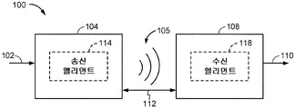
도 1 은 예시적인 실시형태에 따른 무선 전력 전송 시스템 (100) 의 기능 블록 다이어그램이다. 입력 전력 (102) 은 에너지 전송을 수행하기 위한 무선 (예를 들어, 자기 또는 전자기) 장 (105) 을 생성하기 위해 전원 (이 도면에는 나타내지 않음) 으로부터 송신기 (104) 에 제공될 수도 있다. 수신기 (108) 는 무선장 (105) 에 커플링하고 출력 전력 (110) 에 커플링된 디바이스 (이 도면에는 나타내지 않음) 에 의한 저장 또는 소비를 위한 출력 전력 (110) 을 생성한다. 송신기 (104) 및 수신기 (108) 는 거리 (112) 만큼 이격된다. 송신기 (104) 는 수신기 (108) 에 에너지를 송신/커플링하기 위한 전력 송신 엘리먼트 (114) 를 포함할 수도 있다. 수신기 (108) 는 송신기 (104) 로부터 송신된 에너지를 수신 또는 캡처/커플링하기 위한 전력 수신 엘리먼트 (118) 를 포함할 수도 있다.1 is a functional block diagram of a wireless
하나의 예시적인 실시형태에서, 송신기 (104) 및 수신기 (108) 는 상호 공진 관계에 따라 구성될 수도 있다. 수신기 (108) 의 공진 주파수 및 송신기 (104) 의 공진 주파수가 실질적으로 동일하거나 매우 가까울 때, 송신기 (104) 와 수신기 (108) 사이의 송신 손실들이 감소된다. 이로써, 무선 전력 전송은 더 큰 거리에 걸쳐 제공될 수도 있다. 따라서, 공진 유도 커플링 기법들은 다양한 거리에 걸쳐 그리고 여러 유도 전력 송신 및 수신 엘리먼트 구성들로 개선된 효율 및 전력 전송을 허용할 수도 있다.In one exemplary embodiment, the
소정의 실시형태들에서, 무선장 (105) 은 송신기 (104) 의 "근거리장 (near field)" 에 대응할 수도 있다. 근거리장은 전력 송신 엘리먼트 (114) 로부터 멀리 전력을 전력을 최소로 방사하는 전력 송신 엘리먼트 (114) 에서의 전류 및 전하로부터 야기되는 강한 리액티브장 (reactive field) 이 있는 영역에 대응할 수도 있다. 근거리 장은 전력 송신 엘리먼트 (114) 의 약 1 파장 (또는 그 부분) 내에 있는 영역에 대응할 수도 있다.In certain embodiments, the
소정의 실시형태들에서, 효율적인 에너지 전달은 전자기파의 에너지의 대부분을 원거리장 (far field) 으로 전파하기보다는 전력 수신 엘리먼트 (118) 에 무선장 (105) 에서의 에너지의 큰 부분을 커플링함으로써 발생할 수도 있다.In some embodiments, efficient energy transfer may occur by coupling a large portion of the energy in the
소정의 실시형태들에서, 송신기 (104) 는 전력 송신 엘리먼트 (114) 의 공진 주파수에 대응하는 주파수로 시변 자기 (또는 전자기) 장 (105) 을 출력할 수도 있다. 수신기 (108) 가 무선장 (105) 내에 있을 때, 시변 자기 (또는 전자기) 장은 전력 수신 엘리먼트 (118) 에서 전류를 유도할 수도 있다. 상술한 바와 같이, 전력 수신 엘리먼트 (118) 가 전력 송신 엘리먼트 (114) 의 주파수에서 공진하는 공진 회로로서 구성되는 경우, 에너지가 효율적으로 전달될 수도 있다. 전력 수신 엘리먼트 (118) 에서 유도된 교류 전류 (AC) 신호는 부하를 충전하거나 부하에 전력을 공급하기 위해 제공될 수도 있는 직류 전류 (DC) 신호를 생성하도록 정류될 수도 있다.In certain embodiments, the
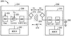
도 2 는 또 다른 예시적인 실시형태에 따른, 무선 전력 전송 시스템 (200) 의 기능 블록 다이어그램이다. 시스템 (200) 은 송신기 (204) 및 수신기 (208) 를 포함할 수도 있다. 송신기 (204)(또한 본 명세서에서는 전력 전송 유닛 PTU 로도 지칭됨) 는 발진기 (222), 드라이버 회로 (224), 및 프론트 엔드 회로 (226) 를 포함할 수도 있는 송신 회로 (206) 를 포함할 수도 있다. 발진기 (222) 는 주파수 제어 신호 (223) 에 응답하여 조정할 수도 있는 원하는 주파수로 발진 신호를 생성하도록 구성될 수도 있다. 발진기 (222) 는 드라이버 회로 (224) 에 발진기 신호를 제공할 수도 있다. 드라이버 회로 (224) 는, 예를 들어 입력 전압 신호 (VD)(225) 에 기초하여 전력 송신 엘리먼트 (214) 의 공진 주파수로 전력 송신 엘리먼트 (214) 를 구동하도록 구성될 수도 있다. 드라이버 회로 (224) 는 발진기 (222) 로부터 구형파를 수신하고 사인파를 출력하도록 구성된 스위칭 증폭기일 수도 있다.2 is a functional block diagram of a wireless
프론트 엔드 회로 (226) 는 고조파 또는 다른 원치 않는 주파수를 필터링하도록 구성된 필터 회로를 포함할 수도 있다. 프론트 엔드 회로 (226) 는 송신기 (204) 의 임피던스를 전력 송신 엘리먼트 (214) 의 임피던스에 매칭하도록 구성된 매칭 회로를 포함할 수도 있다. 하기에서 더 상세하게 설명될 바와 같이, 프론트 엔드 회로 (226) 는 전력 송신 엘리먼트 (214) 와 함께 공진 회로를 생성하기 위해 튜닝 회로를 포함할 수도 있다, 전력 송신 엘리먼트 (214) 를 구동한 결과로서, 전력 송신 엘리먼트 (214) 는 무선장 (205) 을 생성하여 배터리 (236) 를 충전하거나 그렇지 않으면 부하에 전력을 공급하기에 충분한 레벨로 전력을 무선으로 출력할 수도 있다.Front-
송신기 (204) 는 송신 회로부 (206) 에 동작가능하게 커플링되고 송신 회로 부 (206) 의 하나 이상의 양태들을 제어하거나 또는 전력의 전송을 관리하는 것과 관련된 다른 동작들을 달성하도록 구성된 제어기 (240) 를 더 포함할 수도 있다. 제어기 (240) 는 마이크로 제어기 또는 프로세서일 수도 있다. 제어기 (240) 는 주문형 집적 회로 (ASIC) 로서 구현될 수도 있다. 제어기 (240) 는 직접 또는 간접적으로 송신 회로부 (206) 의 각각의 컴포넌트에 동작가능하게 접속될 수도 있다. 제어기 (240) 는 또한 송신 회로부 (206) 의 컴포넌트들의 각각으로부터 정보를 수신하고 수신된 정보에 기초하여 계산들을 수행하도록 구성될 수도 있다. 제어기 (240) 는 그 컴포넌트의 동작을 조정할 수도 있는 컴포넌트들의 각각에 대해 제어 신호 (예를 들어, 신호 (223)) 를 생성하도록 구성될 수도 있다. 이와 같이, 제어기 (240) 는 그에 의해 수행된 동작들의 결과에 기초하여 전력 전송을 조정 또는 관리하도록 구성될 수도 있다. 송신기 (204) 는 예를 들어, 제어기 (240) 로 하여금 무선 전력 전송의 관리와 관련된 것들과 같은, 특정 기능들을 수행하게 하기 위한 명령들과 같은 데이터를 저장하도록 구성된 메모리 (미도시) 를 더 포함할 수도 있다.
수신기 (208)(또한 본 명세서에서는 전력 수신 유닛, PRU 로도 지칭됨) 는 프론트 엔드 회로 (232) 및 정류기 회로 (234) 를 포함할 수도 있는 수신 회로 (210) 를 포함할 수도 있다. 프론트 엔드 회로 (232) 는 전력 수신 엘리먼트 (218) 의 임피던스에 수신 회로 (210) 의 임피던스를 매칭하도록 구성된 매칭 회로를 포함할 수도 있다. 하기에서 설명될 바와 같이, 프론트 엔드 회로 (232) 는 전력 수신 엘리먼트 (218) 로 공진 회로를 생성하기 위해 튜닝 회로를 더 포함할 수도 있다. 정류기 회로 (234) 는, 도 2 에 나타낸 바와 같이, 배터리 (236) 를 충전하기 위해 AC 전력 입력으로부터 DC 전력 출력을 생성할 수도 있다. 수신기 (208) 및 송신기 (204) 는 부가적으로 별도의 통신 채널 (219)(예를 들어, 블루투스 (Bluetooth), 지그비 (Zigbee), 셀룰러 등) 상에서 통신할 수도 있다. 수신기 (208) 및 송신기 (204) 는 대안으로 무선장 (205) 의 특징들을 사용하여 대역내 시그널링을 통해 통신할 수도 있다.The receiver 208 (also referred to herein as a power receiving unit, also referred to as a PRU) may include a receiving
수신기 (208) 는 송신기 (204) 에 의해 송신되고 수신기 (208) 에 의해 수신된 전력의 양이 배터리 (236) 를 충전하기에 적절한지 여부를 결정하도록 구성될 수도 있다. 소정의 실시형태들에서, 송신기 (204) 는 에너지 전달을 제공하기 위해 직접 필드 커플링 계수 (k) 를 갖는 우세한 비방사장을 생성하도록 구성될 수도 있다. 수신기 (208) 는 무선장 (205) 에 직접 커플링할 수도 있고 출력 또는 수신 회로부 (210) 에 커플링된 배터리 (또는 부하)(236) 에 의한 소비 또는 저장을 위한 출력 전력을 생성할 수도 있다.The
수신기 (208) 는 무선 전력 수신기 (208) 의 하나 이상의 양태들을 관리하기 위해 상술한 바와 같이 송신 제어기 (240) 와 유사하게 구성된 제어기 (250) 를 더 포함할 수도 있다. 수신기 (208) 는 예를 들어, 제어기 (250) 로 하여금 무선 전력 전송의 관리와 관련된 것들과 같은 특정 기능들을 수행하게 하는 명령들과 같은, 데이터를 저장하도록 구성된 메모리 (미도시) 를 더 포함할 수도 있다.The
위에 논의된 바와 같이, 송신기 (204) 및 수신기 (208) 는 소정의 거리만큼 분리될 수도 있고, 송신기 (204) 와 수신기 (208) 사이의 송신 손실을 최소화하기 위해 상호 공진 관계에 따라 구성될 수도 있다.As discussed above, the
도 3 은 예시적인 실시형태들에 따른, 도 2 의 송신 회로부 (206) 또는 수신 회로부 (210) 의 일부의 개략적인 다이어그램이다. 도 3 에 도시된 바와 같이, 송신 또는 수신 회로부 (350) 는 전력 송신 또는 수신 엘리먼트 (352) 및 튜닝 회로 (360) 를 포함할 수도 있다. 전력 송신 또는 수신 엘리먼트 (352) 는 또한 안테나 또는 "루프" 안테나로 지칭되거나 구성될 수도 있다. 용어 "안테나"는 일반적으로 다른 안테나에 커플링하기 위해 에너지를 무선으로 출력하거나 수신할 수도 있는 컴포넌트를 지칭한다. 전력 송신 또는 수신 엘리먼트 (352) 는 또한 본 명세서에서 "자기" 안테나 또는 유도 코일, 공진기, 또는 공진기의 일부로서 지칭되거나 구성될 수도 있다. 전력 송신 또는 수신 엘리먼트 (352) 는 또한 전력을 무선으로 출력하거나 수신하도록 구성되는 유형의 코일 또는 공진기로 지칭될 수도 있다. 본 명세서에서 사용된 바와 같이, 전력 송신 또는 수신 엘리먼트 (352) 는 전력을 무선으로 출력 및/또는 수신하도록 구성되는 유형의 "전력 전송 컴포넌트"의 일 예이다. 전력 송신 또는 수신 엘리먼트 (352) 는 페라이트 코어 (이 도면에는 나타내지 않음) 와 같은 물리적 코어 또는 에어 코어를 포함할 수도 있다.FIG. 3 is a schematic diagram of a portion of the transmit
전력 송신 또는 수신 엘리먼트 (352) 가 튜닝 회로 (360) 와 함께 공진 회로 또는 공진기로서 구성될 때, 전력 송신 또는 수신 엘리먼트 (352) 의 공진 주파수는 인덕턴스 및 커패시턴스에 기초할 수도 있다. 인덕턴스는 단순히 전력 송신 또는 수신 엘리먼트 (352) 를 형성하는 코일 및/또는 다른 인덕터에 의해 생성된 인덕턴스일 수도 있다. 커패시턴스 (예를 들어, 커패시터) 는 원하는 공진 주파수에서 공진 구조를 생성하기 위해 튜닝 회로 (360) 에 의해 제공될 수도 있다. 비제한적인 예로서, 튜닝 회로 (360) 는 공진 회로를 생성하기 위해 송신 및/또는 수신 회로 (350) 에 부가될 수도 있는 커패시터 (354) 및 커패시터 (356) 를 포함할 수도 있다.When the power transmitting or receiving
튜닝 회로 (360) 는 전력 송신 또는 수신 엘리먼트 (352) 에 함께 공진 회로를 형성하기 위해 다른 컴포넌트들을 포함할 수도 있다. 다른 비제한적인 예로서, 튜닝 회로 (360) 는 회로부 (350) 의 2 개의 단자들 사이에 병렬로 배치된 커패시터 (미도시) 를 포함할 수도 있다. 여전히 다른 설계들이 가능하다. 일부 실시형태들에서, 프론트 엔드 회로 (226) 에서의 튜닝 회로는 프론트 엔드 회로 (232) 에서의 튜닝 회로와 동일한 설계 (예를 들어, 360) 를 가질 수도 있다. 다른 실시형태들에서, 프론트 엔드 회로 (226) 는 프론트 엔드 회로 (232) 와는 상이한 튜닝 회로 설계를 사용할 수도 있다.The
전력 송신 엘리먼트들에 대해, 전력 송신 또는 수신 엘리먼트 (352) 의 공진 주파수에 실질적으로 대응하는 주파수를 갖는 신호 (358) 는 전력 송신 또는 수신 엘리먼트 (352) 에 대한 입력일 수도 있다. 전력 수신 엘리먼트들에 대해, 송신 또는 수신 엘리먼트 (352) 의 공진 주파수에 실질적으로 대응하는 주파수를 갖는 신호 (358) 는 전력 송신 또는 수신 엘리먼트 (352) 로부터의 출력일 수도 있다. 본 명세서에 개시된 양태들은 일반적으로 공진 무선 전력 전송에 관한 것이지만, 본 명세서에 개시된 양태들은 무선 전력 전송을 위한 비공진 구현에 사용될 수도 있다.For power transmission elements, a
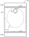
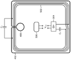
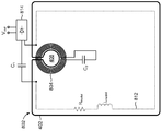
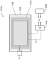
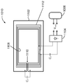
또한, 도 4a 및 도 4b 는 개시물에 따른 전자 디바이스 (40) (예를 들어, 스마트폰, 컴퓨터 테블릿, 랩탑 등) 의 일 예를 도시한다. 전자 디바이스 (40) 는 전자 디바이스 (40) 를 포함하는 전자기기 (미도시) 을 하우징하기 위한 후면 인클로저 (하우징)(400) 를 포함할 수도 있다. 일부 실시형태들에서, 후면 인클로저 (400) 는 금속성 (금속 후면 커버) 일 수도 있다. 일부 실시형태들에서, 후면 인클로저 (400) 는 수 개의 금속성 부분들 (402a, 402, 402b) 로 세분화될 수도 있다. 부분들 (402a 및 402) 은 스페이스 또는 갭 (404) 을 정의하도록 이격될 수도 있다. 통신 안테나들 (미도시) 은 통신 신호들의 송신 및 수신을 가능하게 하기 위해 갭 (404) 에 대해 정렬될 수도 있다. 유사하게, 부분들 (402 및 402b) 은 부가 통신 안테나들 (미도시) 을 위한 스페이스 또는 갭 (406) 을 정의하도록 이격될 수도 있다.4A and 4B also show an example of an electronic device 40 (e.g., a smartphone, a computer tablet, a laptop, etc.) according to the disclosure. The
금속성 부분 (402) 은 후면 인클로저 (400) 의 일부를 정의하도록 형성된 전기 전도성 바디 (구조) 를 포함할 수도 있다. 개시물에 따르면, 금속성 부분 (402) 은 전력 수신 엘리먼트를 정의하기 위해 개방 루프 (412) 의 형상을 가질 수도 있다. 도 4b 는 예를 들어, 금속성 부분 (402) 이 금속성 부분 (402) 을 통해 형성된 개구 (408) 를 정의할 수도 있음을 나타낸다. 예를 들어, 개구 (408) 는 카메라의 렌즈 (미도시) 를 유지하는데 사용될 수도 있다. 슬롯 (410) 은 금속성 부분 (402) 에 의해 정의되고 이를 통해 형성되며 개구 (408) 사이에서 연장하며 금속성 부분 (402) 의 주변의 에지는 개방 루프 (412) 를 정의할 수도 있다. 전류 흐름 (422) 은 와전류의 흐름을 나타내며, 이는 하기에서 설명된다.The
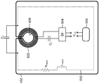
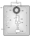
도 5 는 개시물의 양태들에 따른 금속성 부분 (402) 의 부가적인 상세들을 나타내는 개략적 표현이다. 일부 실시형태들에서, 예를 들어 금속성 부분 (402) 은 커패시터 (C1) 에 전기적으로 접속될 수도 있으며, 따라서 회로 (512) 를 생성한다. 도 5 에 도시된 바와 같이, 예를 들어 금속성 부분 (402) 이 개방 루프 (412)(도 4b) 의 형상으로 형성되기 때문에, 금속성 부분 (402) 은 인덕턴스 (Lmodel) 와 직렬로 접속된 저항 (Rmodel) 으로 모델링될 수도 있다. 커패시터 (C1) 는 회로 (512) 를 완성한다.5 is a schematic representation showing additional details of the
일부 실시형태들에서, 전력 수신 엘리먼트 (502) 는 개구 (408) 주위에 감겨진 전기 전도성 재료의 멀티 턴 코일에 의해 정의될 수도 있다. 전력 수신 엘리먼트 (502) 는 금속성 부분 (402) 의 내측 표면에 부착되거나 그렇지 않으면 그 다음에 배치될 수도 있다. 일부 실시형태들에서, 전력 수신 엘리먼트 (502) 는 커패시터 (C2) 에 접속될 수도 있다. 다양한 실시형태들에서, 다른 회로들 또는 회로 엘리먼트들이 커패시터 (C2) 를 대체할 수도 있음이 이해될 것이다. 일부 실시형태들 (미도시) 에서, 커패시터 (C2) 는 생략될 수도 있다.In some embodiments, the
일부 실시형태들에서, 정류하기 위한 수단은 전력 수신 엘리먼트 (502) 에 접속될 수도 있다. 예를 들어, 정류기 (504) 는 전력 수신 엘리먼트 (502) 및 커패시터 (C2) 의 조합에 접속되어 회로 (512) 로부터 전기적으로 분리되는 회로를 정의할 수도 있다. 정류기 (504) 는 직류 전류 (DC) 출력 전압 (Vout)(DC 전력) 을 생성하기 위해 전력 수신 엘리먼트 (502) 에서의 교류 전류 (AC) 신호를 정류하기 위한 임의의 적절한 설계일 수도 있다. 출력 전압 (Vout) 은 전자 디바이스 (40, 도 4a) 에서의 부하 (예를 들어, 디바이스 전자기기)(506) 에 제공될 수도 있다.In some embodiments, the means for rectifying may be connected to the
일부 실시형태들에서, 전력 수신 엘리먼트 (502) 를 포함하는 전기 전도성 재료의 코일은 개구 (408) 에 인접한 개구 (408) 주위에 감겨질 수도 있다. 다른 실시형태들에서, 전력 수신 엘리먼트 (502) 는 개구 (408) 보다 더 큰 영역을 둘러싸도록 더 큰 둘레 주위에 있을 수도 있다. 도 5a 는 예를 들어, 전력 수신 엘리먼트 (502) 가 금속성 부분 (402) 의 주변 주위에 감겨질 수도 있음을 나타낸다. 다른 실시형태에서, 전력 수신 엘리먼트 (502) 의 둘레는 개구 (408) 와 금속성 부분 (402) 의 둘레 사이의 어느 곳에든 놓일 수도 있음을 알 것이다.In some embodiments, a coil of electrically conductive material, including the
도 6 을 참조하면, 동작에 있어서, 금속성 부분 (402) 이 외부 생성 자기장 (예를 들어, 도 1 에 나타낸 무선 전력 전송 시스템 (100) 의 무선장 (105)) 에 노출될 때, 금속성 부분 (402) 은 외부 생성 자기장에 커플링할 수도 있고 이 커플링에 응답하여, 전류의 흐름 (예를 들어, 와전류) 이 금속성 부분 (402) 에서 유도될 수도 있다. 이러한 전류의 흐름은 회로 (512) 에서의 전류 (602) 의 흐름으로서 도면에 개략적으로 나타낸다. 비교를 위해, 도 4b 는 커패시터 (C1) 가 생략될 때 금속성 부분 (402) 에서 유도된 전류 (422) 가 어떻게 흐를 수 있는지를 나타낸다.6, in operation, when the
금속성 부분 (402) 이 저항 (Rmodel) 및 인덕턴스 (Lmodel) 의 직렬 접속으로서 모델링될 수도 있다는 것을 상기하면, 인덕턴스 (Lmodel) 와 직렬 접속된 커패시터 (C1) 는 인덕턴스 (Lmodel) 에 의해 제시된 리액턴스를 소거하거나 적어도 상당히 감소시킬 수도 있다. 원칙적으로, 커패시터 (C1) 의 커패시턴스가 적절하게 선택되면, Lmodel 및 C1 의 리액턴스 컴포넌트들, 각각 ![]()
![]()
![]()
![]()
금속성 부분 (402) 에서 유도된 전류 (602) 의 흐름은 결국 도 6 에서 음영 영역 (604) 으로 개략적으로 도시되는 금속성 부분 (402) 으로부터 발산하는 자기장 (유도 자기장) 을 생성할 수도 있다. 따라서, 금속성 부분 (402) 은 자기장, 즉 유도 자기장 (604) 을 생성하기 위한 수단으로서 작용할 수도 있다. 전력 수신 엘리먼트 (502) 는 결국 유도 자기장 (604) 에 커플링할 수 있으며, 이는 전력 수신 엘리먼트 (502) 에서 전류 (606) 의 흐름을 초래한다. 따라서, 전력 수신 엘리먼트 (502) 는 전류 (606) 의 흐름을 생성하기 위한 수단으로서 작용할 수도 있다.The flow of current 602 induced in the
전력 수신 엘리먼트 (502) 에서 유도된 전류 (606) 의 흐름은 적절한 정류기 (예를 들어, 정류기 (504)) 를 사용하여 정류되어 부하 (506)(예를 들어, 디바이스 전자기기, 배터리 등) 에 전력을 공급하는데 사용될 수 있는 DC 전압 (Vout) 을 생성할 수도 있다. 따라서, 적절하게 선택된 커패시터 (C1) 는 금속성 부분 (402) 에서 전류 (602) 의 유도된 흐름을 최대화할 수 있으며, 이는 결국 전력 수신 엘리먼트 (502) 에 의해 커플링될 수 있는 유도 자기장 (604) 을 최대화할 수 있다.The flow of current 606 derived from the
개시물에 따르면, 금속성 부분 (402) 의 공진 주파수는 회로 (512) 의 공진 주파수를 설정하기 위해 커패시터 (C1) 에 대한 커패시턴스의 적절한 선택에 의해 튜닝 (금속성 부분 (402) 을 "튜닝") 에 의해 조정될 수도 있다. 공진에서, 리액티브 컴포넌트들 (Lmodel 및 C1) 은 특정 주파수에서 실질적으로 소거된다. 마찬가지로, 전력 수신 엘리먼트 (502) 의 공진 주파수는 전력 수신 엘리먼트 (502) 를 포함하는 회로의 공진 주파수를 설정하기 위해 커패시터 (C2) 에 대한 커패시턴스의 적절한 선택에 의해 튜닝될 수도 있다.According to the disclosure, the resonant frequency of the
도 6a 를 참조하면, 개시물에 따라, 송신 코일로부터 전력 수신 엘리먼트 (502) 로의 전력 전송 (예를 들어, 전송된 전력의 양 및 전송의 효율성) 은 송신 코일과 금속성 부분 (402) 사이의 상호 인덕턴스 (M1)(및 이에 따른 커플링) 및/또는 금속성 부분 (402) 과 전력 수신 엘리먼트 (502) 사이의 상호 인덕턴스 (M2) 를 변화시키는 것에 의해 제어될 수도 있다. 예를 들어, 송신 코일과 전력 수신 엘리먼트 (502) 사이의 커플링은 송신 코일과 금속성 부분 (402) 사이의 상호 인덕턴스 (M1) 및 금속성 부분 (402) 과 전력 수신 엘리먼트 (502) 사이의 상호 인덕턴스 (M2) 양자 모두를 최대화함으로써 전력 전송에 대해 최대화될 수도 있다. 최대 상호 인덕턴스는 금속성 부분 (402) 및 전력 수신 엘리먼트 (502) 양자 모두의 공진 주파수가 송신 코일에 의해 생성된 외부 생성 자기장의 주파수와 실질적으로 동일하게 되도록 설정함으로써 달성될 수 있다.6A, power transfer from the transmit coil to the power receiving element 502 (e.g., the amount of transmitted power and the efficiency of transmission) is determined by the interaction between the transmit coil and the
일부 상황들에서, 최대 전력 전송보다 적은 것이 바람직할 수도 있다. 전력 전송의 정도는 상호 인덕턴스를 낮춤으로써 제어될 수도 있다. 예를 들어, 금속성 부분 (402) 의 공진 주파수는, 전력 수신 엘리먼트 (502) 의 공진 주파수를 외부 생성 자기장의 주파수와 실질적으로 동일하게 두면서, 송신 코일과 금속성 부분 (402) 사이의 상호 인덕턴스 (M1) 를 감소시키기 위해 외부 생성 자기장 ("오프 공진" 인 것으로 지칭됨) 의 주파수와 상이한 주파수로 설정될 수도 있다. 송신 코일과 금속성 부분 (402) 사이의 상호 인덕턴스 (M1) 를 감소시키면 송신 코일로부터 전력 수신 엘리먼트 (502) 로의 전력 전송을 감소시키는 전반적인 효과를 가질 수도 있다. 대조적으로, 금속성 부분 (402) 의 공진 주파수는 외부 생성 자기장의 주파수와 실질적으로 동일한 상태를 유지할 수도 있는 한편, 전력 수신 엘리먼트 (502) 의 공진 주파수는 금속성 부분 (402) 과 전력 수신 엘리먼트 (502) 사이의 상호 인덕턴스 (M2) 를 감소시키기 위해 외부 생성 자기장의 주파수와 상이한 주파수로 설정될 수도 있다. 일부 실시형태들에서, 송신 코일과 금속성 부분 (402) 사이의 상호 인덕턴스 (M2) 및 금속성 부분 (402) 과 전력 수신 엘리먼트 (502) 사이의 상호 인덕턴스의 양자 모두는, 예를 들어 금속성 부분 (402) 및 전력 수신 엘리먼트 (502) 의 양자 모두가 외부 생성 자기장의 주파수에 대해 오프 공진이 되도록 튜닝함으로써, 감소될 수도 있다.In some situations, less than maximum power transmission may be desirable. The degree of power transfer may be controlled by lowering the mutual inductance. For example, the resonant frequency of the
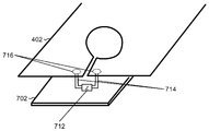
도 5, 도 5a 및 도 6 을 다시 참조하면, 개략적 표현들은 금속성 부분 (402) 에 전기적으로 접속된 커패시터 (C1) 를 도시한다. 일부 실시형태들에서, 커패시터 (C1) 는 금속성 부분 (402) 에 직접 접속 (예를 들어, 솔더링) 될 수도 있다. 다른 실시형태들에서, 커패시터 (C1) 를 금속성 부분 (402) 에 직접 부착하는 것은 실용적이지 않을 수도 있다. 따라서, 도 7 은 개시물의 다른 실시형태들에 따른 커패시터 (C1) 를 사용하여 금속성 부분 (402) 을 튜닝하는 특정 구현의 일 예를 도시한다. 튜닝 엘리먼트 (712) 는 전자 디바이스 (예를 들어, 도 4a 의 40) 의 디바이스 전자기기를 포함하는 인쇄 회로 기판 (PCB)(702) 상에 배치될 수도 있다. PCB (702) 에 부착되고 튜닝 엘리먼트 (712) 에 접속된 커넥터들 (714)(예를 들어, 포고 핀 (pogo pin) 들) 은 튜닝 엘리먼트 (712) 로부터 연장하여 금속성 부분 (402) 상에 형성된 콘택 지점들 (716) 과 전기적으로 콘택하며, 이로써 튜닝 엘리먼트 (712) 를 금속성 부분 (402) 에 전기적으로 접속시킨다.Referring again to Figures 5, 5A and 6, schematic representations show a capacitor C 1 electrically connected to the
다양한 실시형태들에서, 튜닝 엘리먼트 (712) 는 임의의 적절한 회로부 또는 회로 엘리먼트일 수도 있다. 일부 실시형태들에서, 예를 들어 튜닝 엘리먼트 (712) 는 커패시터 (C1)(도 5) 와 같은 커패시터일 수도 있다. 다른 실시형태들에서, 튜닝 엘리먼트 (712) 는 가변 커패시터, 직렬 접속 커패시터들, 병렬 접속 커패시터들 등을 포함하는 커패시터들의 네트워크를 포함할 수도 있다. 위에 언급된 바와 같이, 금속성 부분 (402) 은 그 루프 형상 (412)(도 4b) 에 의해 그와 연관된 인덕턴스 (Lmodel)(도 5) 를 갖는다. 일부 실시형태들에서, 금속성 부분 (402) 의 인덕턴스는 변경될 수도 있다. 따라서, 일부 실시형태들에서, 튜닝 엘리먼트 (712) 는 금속성 부분 (402) 및 튜닝 엘리먼트 (712) 에 의해 제시된 전체 인덕턴스를 증가 또는 감소시키기 위해 하나 이상의 유도성 엘리먼트들을 포함할 수도 있다.In various embodiments, the
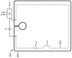
개시물에 따라, 금속성 부분 (402) 및 전력 수신 엘리먼트 (502) 의 역할이 역전될 수도 있다. 도 8 을 참조하면, 예를 들어 일부 실시형태들에서, 금속성 부분 (402) 은 전력 수신 엘리먼트 (802) 로서 작용할 수도 있다. 정류기 (814) 는 회로 (812) 를 정의하기 위해 금속성 부분 (402) 에 접속될 수도 있다. 일부 실시형태들에서, 튜닝 커패시터 (C1)(또는 다른 튜닝 회로) 가 예를 들어 회로 (812) 의 공진 주파수를 튜닝하기 위해 회로 (812) 에 부가될 수도 있다. 자기장을 생성하기 위한 수단은 개구 (408) 주위에 감겨진 전기 전도성 재료의 코일 (804) 을 포함할 수도 있다. 커패시터 (C2) 는 코일 (804) 에 접속되어 코일 (804) 및 커패시터 (C2) 에 의해 정의된 회로의 공진 주파수를 튜닝할 수도 있다.Depending on the disclosure, the role of the
상술한 바와 같이, 송신 코일 (예를 들어, 전력 송신 엘리먼트 (114), 도 1) 로부터 전력 수신 엘리먼트 (802) 로의 전력 전송은 송신 코일과 전력 수신 엘리먼트 (802) 사이의 상호 인덕턴스 및/또는 전력 수신 엘리먼트 (802) 와 코일 (804) 사이의 상호 인덕턴스를 제어함으로써 제어될 수도 있다. 예를 들어, 전력 수신 엘리먼트 (802) 는 송신 코일과 전력 수신 엘리먼트 (802) 사이의 상호 인덕턴스를 변경하기 위해서 송신 코일에 의해 생성된 외부 자기장의 주파수에 대해 공진 또는 오프 공진이 되도록 (예를 들어, C1 를 튜닝함으로써) 튜닝될 수도 있다. 마찬가지로, 코일 (804) 은 전력 수신 엘리먼트 (802) 와 코일 (804) 사이의 상호 인덕턴스를 변경하기 위해서 외부 자기장의 주파수에 대해 공진 또는 오프 공진이 되도록 (예를 들어, C2 를 튜닝함으로써) 튜닝될 수도 있다.As described above, power transfer from a transmit coil (e.g.,
도 8a 를 참조하면, 다른 실시형태들에서, 코일 (804) 이 생략되어, 전력 수신 엘리먼트 (802)(금속성 부분 (402) 을 사용하여 실현됨), 및 커패시터 (C1) 및 정류기 (814) 를 포함하는 공진 회로 (812) 만을 남길 수도 있다.8A, in other embodiments, the
도 9 및 도 9a 를 참조하면, 개시물에 따른 실시형태들은 웨어러블 전자 디바이스를 포함할 수도 있다. 일부 실시형태들에서, 예를 들어 웨어러블 전자 디바이스 (90) 는 파스너 (fastener)(94) 에 접속된 디바이스 바디 (92) 를 포함할 수도 있다. 웨어러블 전자 디바이스 (90) 는 스마트워치, 피트니스 모니터링 디바이스 등일 수도 있다.9 and 9A, embodiments in accordance with the disclosure may include a wearable electronic device. In some embodiments, the wearable
디바이스 바디 (92) 는 금속성 부분 (902) 을 포함할 수도 있다. 금속성 부분 (902) 은 중앙 개구 (908) 를 정의하는 개방 루프 형상 및 개구 (908) 및 금속성 부분 (902) 의 주변을 연결하는 슬롯 (910) 을 가질 수도 있다. 커패시터 (C1) 는 커패시터 (C1) 에 의해 튜닝된 회로를 정의하도록 금속성 부분 (902) 에 접속될 수도 있다. 디바이스 바디 (92) 는 개구 (908) 주위에 감겨진 전력 수신 엘리먼트 (예를 들어, 코일)(912) 를 포함할 수도 있다. 전력 수신 엘리먼트 (912) 는 (예를 들어, 전력 수신 엘리먼트 (912) 를 튜닝하기 위해) 커패시터 (C2) 에, 그리고 정류기 (904) 에 접속되어 외부 생성 자기장에 노출될 때 전력 수신 엘리먼트 (912) 에서 유도된 전류의 흐름을 사용하여 DC 전압 (Vout) 을 생성할 수도 있다.The
일부 실시형태들에서, 금속성 부분 (902) 은 웨어러블 디바이스 (90) 를 포함하는 디바이스 전자기기 (미도시) 을 하우징하는 하우징으로서 작용할 수도 있다. 도 9a 를 참조하면, 다른 실시형태들에서, 웨어러블 전자 디바이스 (91) 는 전력 수신 엘리먼트 (912) 및 금속성 부분 (902) 을 하우징하는 비금속성 하우징 (96) 을 포함할 수도 있는 디바이스 바디 (93) 를 포함할 수도 있다.In some embodiments, the
상술한 바와 같이, 송신 코일 (예를 들어, 전력 송신 엘리먼트 (114), 도 1) 로부터 전력 수신 엘리먼트 (912) 로의 전력 전송은 송신 코일과 전력 수신 엘리먼트 (912) 사이의 상호 인덕턴스 및/또는 전력 수신 엘리먼트 (912) 와 금속성 부분 (902) 사이의 상호 인덕턴스를 제어하는 것에 의해 제어될 수도 있다. 예를 들어, 전력 수신 엘리먼트 (912) 는 송신 코일과 전력 수신 엘리먼트 (912) 사이의 상호 인덕턴스를 변경하기 위해 송신 코일에 의해 생성된 외부 자기장의 주파수에 대해 공진 또는 오프 공진이 되도록 (예를 들어, C2 를 튜닝하는 것에 의해) 튜닝될 수도 있다. 마찬가지로, 금속성 부분 (902) 은 전력 수신 엘리먼트 (912) 와 금속성 부분 (902) 사이의 상호 인덕턴스를 변경하기 위해서 외부 자기장의 주파수에 대해 공진 또는 오프 공진이 되도록 (예를 들어, C1 을 튜닝하는 것에 의해) 튜닝될 수도 있다.As described above, the power transfer from the transmit coil (e.g.,
도 10 을 참조하면, 개시물에 따른 실시형태들은 휴대용 컴퓨터들; 예를 들어, 랩탑 컴퓨터들, 컴퓨터 테블릿들 등을 포함할 수도 있다. 일부 실시형태들에서, 예를 들어 휴대용 컴퓨터 (10) 는 무선 전력 수신기 (1010), 및 디스플레이 (1004) 및 디바이스 전자기기 (예를 들어, 회로부, 배터리 등)(1006) 을 하우징하기 위해 전면 인클로저 (1002) 및 후면 인클로저 (1008) 를 포함할 수도 있다. 후면 인클로저 (1008) 는 무선 전력 수신 기능과 간섭하지 않도록 비금속성 재료일 수도 있다. 이제 개시물에 따른 무선 전력 수신기 (1010) 의 상세들이 기재될 것이다.10, embodiments in accordance with the disclosure include portable computers; For example, laptop computers, computer tables, and the like. In some embodiments, for example, the
도 11a 및 도 11b 는 개시물의 실시형태들에 따른 무선 전력 수신기 (1010) 의 상세들을 나타내는 개략적인 표현들이다. 무선 전력 수신기 (1010) 는 금속성 부분 (1102) 의 주변과 개구 (1108) 사이를 연장하는 슬롯 (1110) 및 개구 (1108) 를 정의하는 개방 루프의 형상을 갖는 금속성 부분 (1102) 을 포함할 수도 있다. 전력 수신 엘리먼트 (예를 들어, 코일)(1112) 는 개구 (1108) 주위에 감겨질 수도 있다. 정류기 (1104) 는 외부 생성 자기장에 응답하여 전력 수신 엘리먼트 (1112) 에서 일어날 수 있는 전류의 흐름으로부터 DC 전압 (Vout) 을 생성하기 위해 전력 수신 엘리먼트 (1112) 에 접속될 수도 있다.11A and 11B are schematic representations illustrating details of a
페라이트 층 (1122) 은 디바이스 전자기기 (1006) 에 커플링하는 것으로부터 전력 수신기 (1010) 에 의해 생성될 수 있는 자기장을 방지하기 위해, 전력 수신 엘리먼트 (1112) 와 디바이스 전자기기 (1006) 사이에 배치될 수도 있다. 폐라이트 층 (1122) 은 금속성 부분 (1102) 의 상세들을 명확히 도시하기 위해 도 11b 에서는 생략된다.The
커패시터 (C1) 는 금속성 부분 (1102) 과 송신 코일 사이의 상호 인덕턴스를 변경하기 위해서 외부 생성 자기장과 공진에 또는 외부 생성 자기장과 공진 외에 있도록 금속성 부분 (1102) 을 튜닝하는데 사용될 수도 있다. 유사하게, 커패시터 (C2) 는 전력 수신 엘리먼트 (1112) 와 금속성 부분 (1102) 사이의 상호 인덕턴스를 변경하기 위해서 외부 생성 자기장과 공진에 또는 공진 외에 있도록 전력 수신 엘리먼트 (1112) 를 튜닝하는데 사용될 수도 있다.The capacitor C 1 may be used to tune the
개시물의 실시형태들에 따라, 전력 수신기 (1010) 는 도 10 에 나타낸 휴대용 컴퓨터의 면적보다 더 작은 면적을 가질 수도 있다. 일부 실시형태들에서, 전력 수신기 (1010) 의 면적은 포터블 컴퓨터 (10) 의 면적의 50% 미만일 수도 있다. 튜닝된 금속성 부분 (1102) 의 증폭 효과로 인해, 코일 (1112) 은 외부 생성 자기장에 더 강하게 커플링하고, 이로써 튜닝된 금속성 부분 (1112) 과 같은 증폭 엘리먼트를 사용하지 않는 무선 전력 전송 시스템에서 더 큰 전력 전송을 달성할 수도 있다. 따라서, 전력 수신기 (1010) 는 더 작으며 더 큰 무선 전력 전송 시스템과 비교하여 여전히 유사한 전력 전송을 달성할 수도 있다.According to embodiments of the disclosure, the
상기 설명은 특정 실시형태들의 양태들이 어떻게 구현될 수 있는지의 예들과 함께 개시물의 다양한 실시형태들을 예시한다. 상기 예들은 유일한 실시형태들인 것으로 간주되지 않아야 하며 다음의 청구항들에 의해 정의된 바와 같이 특정 실시형태들의 유연성 및 이점들을 예시하기 위해 제시된다. 상기 개시물 및 다음의 청구항들에 기초하여, 다른 배열들, 실시형태들, 구현들 및 등가물들이 청구항들에 의해 정의된 바와 같은 개시물의 범위로부터 벗어나지 않으면서 채용될 수도 있다.The above description illustrates various embodiments of the disclosure with examples of how aspects of certain embodiments may be implemented. The above examples are not to be considered as unique embodiments and are presented to illustrate the flexibility and advantages of certain embodiments as defined by the following claims. Other arrangements, embodiments, implementations, and equivalents may be employed without departing from the scope of the disclosure as defined by the claims, based on the foregoing disclosure and the following claims.
Claims (30)
제 1 자기장에 자기적으로 커플링하도록 구성된 전기 전도성 바디;
상기 전기 전도성 바디에 전기적으로 접속된 제 1 튜닝 엘리먼트; 및
상기 전기 전도성 바디에 의해 정의된 개구 주위에 감겨진 전기 전도성 코일로서, 상기 전기 전도성 코일은 제 2 자기장에 자기적으로 커플링하도록 구성되는, 상기 전기 전도성 코일을 포함하는, 무선 전력 전송을 위한 전자 장치.An electronic device for wireless power transmission,
An electrically conductive body configured to magnetically couple to a first magnetic field;
A first tuning element electrically connected to the electrically conductive body; And
An electrically conductive coil wound about an aperture defined by the electrically conductive body, the electrically conductive coil being configured to magnetically couple to a second magnetic field; Device.
상기 전기 전도성 코일에 전기적으로 접속된 제 2 튜닝 엘리먼트를 더 포함하는, 무선 전력 전송을 위한 전자 장치.The method according to claim 1,
And a second tuning element electrically connected to the electrically conductive coil.
상기 제 1 튜닝 엘리먼트 및 상기 제 2 튜닝 엘리먼트의 각각은 하나 이상의 커패시터들을 포함하는, 무선 전력 전송을 위한 전자 장치.3. The method of claim 2,
Wherein each of the first tuning element and the second tuning element comprises one or more capacitors.
상기 제 1 튜닝 엘리먼트 및 상기 제 2 튜닝 엘리먼트 중 어느 하나 또는 양자 모두가 하나 이상의 인덕터들을 포함하는, 무선 전력 전송을 위한 전자 장치.The method of claim 3,
Wherein either or both of the first tuning element and the second tuning element comprise one or more inductors.
상기 제 1 자기장은 무선 전력 송신기에 의해 생성된 외부 생성 자기장이고, 상기 전기 전도성 바디는 상기 외부 생성 자기장에 커플링되는 것에 응답하여 상기 제 2 자기장을 생성하도록 구성되는, 무선 전력 전송을 위한 전자 장치.The method according to claim 1,
Wherein the first magnetic field is an externally generated magnetic field generated by a wireless power transmitter and the electrically conductive body is configured to generate the second magnetic field in response to being coupled to the externally generated magnetic field. .
상기 전기 전도성 코일에 접속된 정류기를 더 포함하고,
상기 정류기는 상기 장치를 포함하는 전자기기에 전력을 제공하기 위해 상기 전기 전도성 코일에서 유도된 전류를 정류하도록 구성되는, 무선 전력 전송을 위한 전자 장치.6. The method of claim 5,
Further comprising a rectifier connected to the electrically conductive coil,
Wherein the rectifier is configured to rectify the current induced in the electrically conductive coil to provide power to the electronic device including the device.
상기 제 2 자기장은 외부 생성 자기장이고, 상기 전기 전도성 코일은 상기 외부 생성 자기장에 커플링되는 것에 응답하여 상기 제 1 자기장을 생성하도록 구성되며, 상기 장치는 상기 전기 전도성 바디에 접속된 정류기를 더 포함하고, 상기 정류기는 상기 장치를 포함하는 전자기기에 전력을 제공하기 위해 상기 전기 전도성 바디에서 유도된 전류를 정류하도록 구성되는, 무선 전력 전송을 위한 전자 장치.The method according to claim 1,
Wherein the second magnetic field is an externally generated magnetic field and the electrically conductive coil is configured to generate the first magnetic field in response to being coupled to the externally generated magnetic field, the device further comprising a rectifier connected to the electrically conductive body And the rectifier is configured to rectify the current induced in the electrically conductive body to provide power to the electronic device including the device.
상기 제 1 튜닝 엘리먼트가 상부에 배치된 인쇄 회로 기판; 및
상기 전기 전도성 바디에 상기 제 1 튜닝 엘리먼트를 전기적으로 접속하는 커넥터를 더 포함하는, 무선 전력 전송을 위한 전자 장치.The method according to claim 1,
A printed circuit board on which the first tuning element is disposed; And
Further comprising a connector for electrically connecting the first tuning element to the electrically conductive body.
인쇄 회로 기판을 더 포함하고, 상기 전기 전도성 코일은 상기 전기 전도성 바디와 상기 인쇄 회로 기판 사이에 배치되는, 무선 전력 전송을 위한 전자 장치.The method according to claim 1,
Further comprising a printed circuit board, wherein the electrically conductive coil is disposed between the electrically conductive body and the printed circuit board.
상기 전기 전도성 코일과 상기 인쇄 회로 기판 사이에 배치된 페라이트 재료를 더 포함하는, 무선 전력 전송을 위한 전자 장치.10. The method of claim 9,
Further comprising a ferrite material disposed between the electrically conductive coil and the printed circuit board.
상기 제 1 튜닝 엘리먼트 및 상기 전기 전도성 바디는 상기 제 1 튜닝 엘리먼트에 의해 정의된 공진 주파수를 갖는 회로를 구성하는, 무선 전력 전송을 위한 전자 장치.The method according to claim 1,
Wherein the first tuning element and the electrically conductive body constitute a circuit having a resonant frequency defined by the first tuning element.
상기 제 1 튜닝 엘리먼트 및 상기 전기 전도성 바디를 포함하는 상기 회로의 공진 주파수와 실질적으로 동일한 공진 주파수를 갖는 회로를 정의하도록 상기 전기 전도성 코일에 전기적으로 접속된 제 2 튜닝 엘리먼트를 더 포함하는, 무선 전력 전송을 위한 전자 장치.12. The method of claim 11,
Further comprising a second tuning element electrically connected to the electrically conductive coil to define a circuit having a resonant frequency substantially equal to a resonant frequency of the circuit comprising the first tuning element and the electrically conductive body, An electronic device for transmission.
상기 제 1 튜닝 엘리먼트 및 상기 전기 전도성 바디를 포함하는 상기 회로의 공진 주파수와 상이한 공진 주파수를 갖는 회로를 정의하도록 상기 전기 전도성 코일에 전기적으로 접속된 제 2 튜닝 엘리먼트를 더 포함하는, 무선 전력 전송을 위한 전자 장치.12. The method of claim 11,
Further comprising a second tuning element electrically connected to the electrically conductive coil to define a circuit having a resonant frequency different from a resonant frequency of the circuit comprising the first tuning element and the electrically conductive body. ≪ / RTI >
전자기기를 하우징하도록 구성된 금속성 인클로저를 더 포함하고, 상기 금속성 인클로저는 상기 전기 전도성 바디를 포함하는, 무선 전력 전송을 위한 전자 장치.The method according to claim 1,
An electronic device for wireless power transmission, further comprising a metallic enclosure configured to house an electronic device, the metallic enclosure including the electrically conductive body.
상기 장치를 포함하는 전자기기를 하우징하도록 구성된 비금속성 인클로저를 더 포함하고, 상기 전기 전도성 바디 및 상기 전기 전도성 코일은 상기 인클로저 내에 하우징되는, 무선 전력 전송을 위한 전자 장치.The method according to claim 1,
Further comprising a non-metallic enclosure configured to house an electronic device including the device, wherein the electrically conductive body and the electrically conductive coil are housed within the enclosure.
상기 장치는 웨어러블 전자 디바이스인, 무선 전력 전송을 위한 전자 장치.The method according to claim 1,
Wherein the device is a wearable electronic device.
전기 전도성 구조로부터 발산하는 유도 자기장을 생성하기 위해, 상기 전자 디바이스에 대한 하우징을 포함하는, 상기 전기 전도성 구조를 통해 외부 생성 자기장에 자기적으로 커플링하는 단계;
전력 수신 엘리먼트에서 전류를 유도하기 위해 상기 전력 수신 엘리먼트를 통해 상기 유도 자기장에 자기적으로 커플링하는 단계로서, 상기 전력 수신 엘리먼트는 상기 전기 전도성 구조로부터 전기적으로 격리되는, 상기 유도 자기장에 자기적으로 커플링하는 단계; 및
상기 전력 수신 엘리먼트에서 유도된 전류로부터 전력을 생성하는 단계를 포함하는, 전자 디바이스로의 무선 전력 전송을 위한 방법.CLAIMS 1. A method for wireless power transmission to an electronic device,
Magnetically coupling to an externally generated magnetic field through the electrically conductive structure, including a housing for the electronic device, to create an induced magnetic field emanating from the electrically conductive structure;
Magnetically coupling to the induced magnetic field through the power receiving element to induce a current in the power receiving element, the power receiving element being magnetically coupled to the induced magnetic field, wherein the induced magnetic field is electrically isolated from the electrically conductive structure Coupling; And
And generating power from the current induced in the power receiving element. ≪ Desc / Clms Page number 21 >
상기 전기 전도성 구조를 포함하는 회로의 공진 주파수는 상기 외부 생성 자기장의 주파수와 실질적으로 동일한, 전자 디바이스로의 무선 전력 전송을 위한 방법.18. The method of claim 17,
Wherein the resonant frequency of the circuit comprising the electrically conductive structure is substantially equal to the frequency of the externally generated magnetic field.
상기 전력 수신 엘리먼트를 포함하는 회로의 공진 주파수는 상기 외부 생성 자기장의 주파수와 실질적으로 동일한, 전자 디바이스로의 무선 전력 전송을 위한 방법.18. The method of claim 17,
Wherein the resonant frequency of the circuit comprising the power receiving element is substantially equal to the frequency of the externally generated magnetic field.
상기 전기 전도성 구조를 통해 상기 외부 생성 자기장에 자기적으로 커플링하는 단계는, 제 1 튜닝 엘리먼트에 전기적으로 접속된 전기 전도성 구조를 포함하는 제 1 회로에서 전류를 유도하는 단계를 포함하고, 상기 전력 수신 엘리먼트를 통해 상기 유도 자기장에 자기적으로 커플링하는 단계는, 제 2 튜닝 엘리먼트에 전기적으로 접속된 상기 전력 수신 엘리먼트를 포함하는 제 2 회로에서 전류를 유도하는 단계를 포함하는, 전자 디바이스로의 무선 전력 전송을 위한 방법.18. The method of claim 17,
Wherein magnetically coupling to the externally generated magnetic field through the electrically conductive structure comprises inducing a current in a first circuit comprising an electrically conductive structure electrically connected to the first tuning element, Wherein magnetically coupling to the induced magnetic field through a receive element comprises inducing a current in a second circuit comprising the power receiving element electrically connected to the second tuning element. Method for wireless power transmission.
상기 제 1 회로 및 상기 제 2 회로 중 어느 하나 또는 양자 모두의 공진 주파수는 상기 외부 생성 자기장의 주파수와 실질적으로 동일한, 전자 디바이스로의 무선 전력 전송을 위한 방법.21. The method of claim 20,
Wherein the resonant frequency of either or both of the first circuit and the second circuit is substantially equal to the frequency of the externally generated magnetic field.
상기 전력을 생성하는 단계는, 상기 전력 수신 엘리먼트에서 유도된 전류를 정류하는 단계를 포함하는, 전자 디바이스로의 무선 전력 전송을 위한 방법.18. The method of claim 17,
Wherein the step of generating the power comprises rectifying the current induced in the power receiving element.
상기 장치를 포함하는 전자 컴포넌트들을 인클로징하도록 구성된 하우징으로서, 상기 하우징은 금속성 부분을 포함하는, 상기 하우징;
상기 하우징의 상기 금속성 부분에 접속된 제 1 튜닝 엘리먼트로서, 상기 하우징의 상기 금속성 부분은 외부 생성 자기장에 자기적으로 커플링되는 것에 응답하여 그 내부에 전류의 흐름이 유도되도록 하는 형상을 가지며, 유도 자기장은 상기 전류의 흐름에 응답하여 상기 금속성 부분으로부터 발산하는, 상기 제 1 튜닝 엘리먼트;
전기 전도성 코일로서, 상기 유도 자기장에 자기적으로 커플링되는 것에 응답하여 상기 전기 전도성 코일에서 전류의 흐름이 유도되는, 상기 전기 전도성 코일; 및
부하에 전력을 제공하기 위해 상기 전기 전도성 코일에서 유도된 전류를 정류하도록 구성된 정류기를 포함하는, 전력을 무선으로 수신하기 위한 장치.An apparatus for wirelessly receiving power,
A housing configured to enclose electronic components comprising the apparatus, the housing including a metallic portion;
A first tuning element connected to the metallic portion of the housing, the metallic portion of the housing being shaped to induce a flow of current therein in response to being magnetically coupled to an externally generated magnetic field, The magnetic field radiating from the metallic portion in response to the flow of current, the first tuning element;
13. An electrically conductive coil, said electrically conductive coil having a current flow induced in said electrically conductive coil in response to being magnetically coupled to said induced magnetic field; And
And a rectifier configured to rectify the current induced in the electrically conductive coil to provide power to the load.
상기 하우징의 상기 금속성 부분은 관통하는 개구를 정의하고 상기 개구로부터 상기 금속성 부분의 주변까지 슬롯을 정의하는, 전력을 무선으로 수신하기 위한 장치.24. The method of claim 23,
Wherein the metallic portion of the housing defines an opening therethrough and defines a slot from the opening to a periphery of the metallic portion.
상기 정류기는 상기 전기 전도성 코일에 전기적으로 접속되는, 전력을 무선으로 수신하기 위한 장치.24. The method of claim 23,
The rectifier being electrically connected to the electrically conductive coil.
상기 제 1 튜닝 엘리먼트 및 상기 하우징의 상기 금속성 부분은 상기 전기 전도성 코일 및 제 2 튜닝 엘리먼트에 의해 정의된 공진 주파수와 실질적으로 동일한 공진 주파수를 정의하는, 전력을 무선으로 수신하기 위한 장치.24. The method of claim 23,
Wherein the first tuning element and the metallic portion of the housing define a resonant frequency substantially equal to a resonant frequency defined by the electrically conductive coil and the second tuning element.
상기 제 1 튜닝 엘리먼트 및 상기 하우징의 상기 금속성 부분은 상기 전기 전도성 코일 및 제 2 튜닝 엘리먼트에 의해 정의된 공진 주파수와 상이한 공진 주파수를 정의하는, 전력을 무선으로 수신하기 위한 장치.24. The method of claim 23,
Wherein the first tuning element and the metallic portion of the housing define a resonant frequency different from a resonant frequency defined by the electrically conductive coil and the second tuning element.
상기 전자 디바이스의 전자기기를 하우징하기 위한 수단으로서, 상기 하우징하기 위한 수단은 외부 생성 자기장에 자기적으로 커플링하기 위한 수단으로부터 발산하는 유도 자기장을 생성하기 위해 상기 외부 생성 자기장에 자기적으로 커플링하기 위한 수단을 포함하는 금속성 부분을 가지며, 상기 외부 생성 자기장에 자기적으로 커플링하기 위한 수단은 공진 주파수에서 공진하기 위해 상기 외부 생성 자기장에 자기적으로 커플링하기 위한 수단을 튜닝하기 위한 수단에 전기적으로 접속되는, 상기 하우징하기 위한 수단;
전류를 유도하기 위해 상기 유도 자기장에 자기적으로 커플링하기 위한 수단으로서, 상기 유도 자기장에 자기적으로 커플링하기 위한 수단은 상기 외부 생성 자기장에 자기적으로 커플링하기 위한 수단으로부터 전기적으로 격리되는, 상기 자기적으로 커플링하기 위한 수단; 및
상기 유도 자기장에 자기적으로 커플링하기 위한 수단에서 유도된 상기 전류로부터 전력을 생성하기 위한 수단을 포함하는, 전자 디바이스에서 전력을 무선으로 수신하기 위한 장치.An apparatus for wirelessly receiving power in an electronic device,
Means for housing an electronic device of the electronic device, the means for housing magnetically coupling to the externally generated magnetic field to generate an induced magnetic field emanating from means for magnetically coupling to an externally generated magnetic field, Wherein the means for magnetically coupling to the externally generated magnetic field comprises means for tuning the means for magnetically coupling to the externally generated magnetic field to resonate at a resonant frequency Means for said housing being electrically connected;
Means for magnetically coupling to the induced magnetic field to induce a current, the means for magnetically coupling to the induced magnetic field being electrically isolated from the means for magnetically coupling to the externally generated magnetic field Means for magnetically coupling said magnetic field; And
And means for generating power from the current induced in the means for magnetically coupling to the induced magnetic field.
상기 외부 생성 자기장에 자기적으로 커플링하기 위한 수단 및 상기 유도 자기장에 자기적으로 커플링하기 위한 수단 중 어느 하나 또는 양자 모두는 상기 외부 생성 자기장의 주파수와 실질적으로 동일한 공진 주파수를 갖는, 전자 디바이스에서 전력을 무선으로 수신하기 위한 장치.29. The method of claim 28,
Wherein either or both of the means for magnetically coupling to the externally generated magnetic field and the means for magnetically coupling to the induced magnetic field have a resonant frequency substantially equal to the frequency of the externally generated magnetic field, For receiving power wirelessly.
상기 유도 자기장에 자기적으로 커플링하기 위한 수단은 전기 전도성 코일을 포함하는, 전자 디바이스에서 전력을 무선으로 수신하기 위한 장치.29. The method of claim 28,
Wherein the means for magnetically coupling to the induced magnetic field comprises an electrically conductive coil.
Applications Claiming Priority (5)
| Application Number | Priority Date | Filing Date | Title |
|---|---|---|---|
| US201662288685P | 2016-01-29 | 2016-01-29 | |
| US62/288,685 | 2016-01-29 | ||
| US15/231,325 | 2016-08-08 | ||
| US15/231,325 US10333334B2 (en) | 2016-01-29 | 2016-08-08 | Wireless power transfer in an electronic device having a tuned metallic body |
| PCT/US2017/012072 WO2017131931A1 (en) | 2016-01-29 | 2017-01-04 | Wireless power transfer in an electronic device having a tuned metallic body |
Publications (1)
| Publication Number | Publication Date |
|---|---|
| KR20180105655A true KR20180105655A (en) | 2018-09-28 |
Family
ID=59385744
Family Applications (1)
| Application Number | Title | Priority Date | Filing Date |
|---|---|---|---|
| KR1020187021255A KR20180105655A (en) | 2016-01-29 | 2017-01-04 | Wireless power transmission in an electronic device with a tuned metallic body |
Country Status (8)
| Country | Link |
|---|---|
| US (2) | US10333334B2 (en) |
| EP (1) | EP3408915B1 (en) |
| JP (1) | JP2019512197A (en) |
| KR (1) | KR20180105655A (en) |
| CN (1) | CN108684208A (en) |
| AU (1) | AU2017211647B2 (en) |
| TW (1) | TW201801445A (en) |
| WO (2) | WO2017131916A1 (en) |
Families Citing this family (4)
| Publication number | Priority date | Publication date | Assignee | Title |
|---|---|---|---|---|
| US10333334B2 (en) | 2016-01-29 | 2019-06-25 | Qualcomm Incorporated | Wireless power transfer in an electronic device having a tuned metallic body |
| US10505254B2 (en) * | 2017-07-28 | 2019-12-10 | Stmicroelectronics, Inc. | Antenna design for active load modulation in a near field communication transponder device |
| US10462417B2 (en) * | 2017-08-31 | 2019-10-29 | Apple Inc. | Methods and apparatus for reducing electromagnetic interference resultant from data transmission over a high-speed audio/visual interface |
| US10629533B2 (en) | 2018-03-13 | 2020-04-21 | Toshiba Memory Corporation | Power island segmentation for selective bond-out |
Family Cites Families (41)
| Publication number | Priority date | Publication date | Assignee | Title |
|---|---|---|---|---|
| US7521890B2 (en) | 2005-12-27 | 2009-04-21 | Power Science Inc. | System and method for selective transfer of radio frequency power |
| JPWO2009031639A1 (en) * | 2007-09-06 | 2010-12-16 | 昭和電工株式会社 | Non-contact rechargeable power storage device |
| US8855554B2 (en) * | 2008-03-05 | 2014-10-07 | Qualcomm Incorporated | Packaging and details of a wireless power device |
| US20120112691A1 (en) | 2008-09-27 | 2012-05-10 | Kurs Andre B | Wireless energy transfer for vehicles |
| US20120248981A1 (en) | 2008-09-27 | 2012-10-04 | Aristeidis Karalis | Multi-resonator wireless energy transfer for lighting |
| US8907531B2 (en) | 2008-09-27 | 2014-12-09 | Witricity Corporation | Wireless energy transfer with variable size resonators for medical applications |
| US20120242159A1 (en) | 2008-09-27 | 2012-09-27 | Herbert Toby Lou | Multi-resonator wireless energy transfer for appliances |
| US20160087687A1 (en) | 2008-09-27 | 2016-03-24 | Witricity Corporation | Communication in a wireless power transmission system |
| EP2396796A4 (en) | 2009-02-13 | 2017-03-22 | Witricity Corporation | Wireless energy transfer in lossy environments |
| US9013141B2 (en) * | 2009-04-28 | 2015-04-21 | Qualcomm Incorporated | Parasitic devices for wireless power transfer |
| US9088307B2 (en) * | 2010-12-29 | 2015-07-21 | National Semiconductor Corporation | Non-resonant and quasi-resonant system for wireless power transmission to multiple receivers |
| JP2012143146A (en) * | 2011-01-03 | 2012-07-26 | Samsung Electronics Co Ltd | Wireless power transmission apparatus and wireless power transmission system thereof |
| EP2691996A4 (en) | 2011-03-30 | 2015-01-28 | Ambature Inc | Electrical, mechanical, computing, and/or other devices formed of extremely low resistance materials |
| US9496755B2 (en) | 2011-09-26 | 2016-11-15 | Qualcomm Incorporated | Systems, methods, and apparatus for rectifier filtering for input waveform shaping |
| US20130127252A1 (en) | 2011-11-17 | 2013-05-23 | William S. Yerazunis | Wireless Energy Transfer with Perfect Magnetic Conductors |
| US9225388B2 (en) | 2012-07-03 | 2015-12-29 | Intel Corporation | Transmitting magnetic field through metal chassis using fractal surfaces |
| AU2013293562B2 (en) | 2012-07-25 | 2017-04-13 | Master Lock Company Llc | Integrated antenna coil in a metallic body |
| JP6061620B2 (en) * | 2012-10-30 | 2017-01-18 | キヤノン株式会社 | Electronic device, control method, and computer program |
| JP5598641B1 (en) * | 2012-12-20 | 2014-10-01 | 株式会社村田製作所 | Information terminal equipment |
| US9876535B2 (en) | 2013-02-21 | 2018-01-23 | Qualcomm Incorporated | Modular inductive power transfer power supply and method of operation |
| JP6117947B2 (en) * | 2013-02-22 | 2017-04-19 | ノキア テクノロジーズ オサケユイチア | Apparatus and method for wireless coupling |
| CN206564323U (en) * | 2013-04-08 | 2017-10-17 | 株式会社村田制作所 | Communication terminal |
| US9431169B2 (en) | 2013-06-07 | 2016-08-30 | Qualcomm Incorporated | Primary power supply tuning network for two coil device and method of operation |
| US20150009077A1 (en) * | 2013-07-03 | 2015-01-08 | Samsung Electronics Co., Ltd. | Cover of a mobile device and mobile device including the same |
| JP5880797B2 (en) * | 2013-09-17 | 2016-03-09 | 株式会社村田製作所 | Camera module and electronic equipment |
| JP6348977B2 (en) | 2013-11-08 | 2018-06-27 | ノキア テクノロジーズ オーユー | Coil configuration with communication coil and induction coil |
| CN103560598A (en) * | 2013-11-12 | 2014-02-05 | 天津工业大学 | Enhanced type electromagnetic resonance subway wireless power supply system |
| US9461500B2 (en) | 2013-11-21 | 2016-10-04 | Htc Corporation | Wireless charging receiving device and wireless charging system using the same |
| JP6297863B2 (en) * | 2014-03-03 | 2018-03-20 | Ihi運搬機械株式会社 | Non-contact power feeding system and vehicle power feeding device |
| US9730002B2 (en) | 2014-04-10 | 2017-08-08 | Avago Technologies General Ip (Singapore) Pte. Ltd. | Mechanical enclosures for a communication device |
| US10381875B2 (en) | 2014-07-07 | 2019-08-13 | Qualcomm Incorporated | Wireless power transfer through a metal object |
| US20160111889A1 (en) | 2014-10-20 | 2016-04-21 | Qualcomm Incorporated | Segmented conductive back cover for wireless power transfer |
| CN104333149B (en) | 2014-11-13 | 2017-03-01 | 矽力杰半导体技术(杭州)有限公司 | Tuning circuit, tuning methods and mode of resonance contactless power supply device |
| US10581284B2 (en) | 2014-12-16 | 2020-03-03 | Samsung Electronics Co., Ltd. | Wireless charger and wireless power receiver |
| CN104821667B (en) * | 2015-03-16 | 2017-02-22 | 中国计量学院 | Magnetic coupling resonant wireless electric energy transmission device based on low frequency PWM rectifier |
| US10476304B2 (en) | 2015-05-27 | 2019-11-12 | Qualcomm Incorporated | Wireless power receive coil for metal backed device |
| CN105119036B (en) | 2015-09-18 | 2019-03-15 | 深圳市信维通信股份有限公司 | A kind of near-field communication and wireless charging integral antenna based on metal rear shell |
| US10361588B2 (en) | 2015-12-07 | 2019-07-23 | Qualcomm Incorporated | Coupled resonator in a metal back cover |
| US20170170689A1 (en) | 2015-12-14 | 2017-06-15 | Qualcomm Incorporated | Wireless charging of metal framed electronic devices |
| US10333334B2 (en) * | 2016-01-29 | 2019-06-25 | Qualcomm Incorporated | Wireless power transfer in an electronic device having a tuned metallic body |
| US9827430B1 (en) | 2017-02-02 | 2017-11-28 | Qualcomm Incorporated | Injected conductive tattoos for powering implants |
-
2016
- 2016-08-08 US US15/231,325 patent/US10333334B2/en active Active
- 2016-09-14 US US15/265,395 patent/US10312716B2/en active Active
- 2016-12-28 WO PCT/US2016/068829 patent/WO2017131916A1/en active Application Filing
-
2017
- 2017-01-04 WO PCT/US2017/012072 patent/WO2017131931A1/en active Application Filing
- 2017-01-04 JP JP2018538814A patent/JP2019512197A/en active Pending
- 2017-01-04 CN CN201780008384.3A patent/CN108684208A/en active Pending
- 2017-01-04 EP EP17700587.3A patent/EP3408915B1/en active Active
- 2017-01-04 AU AU2017211647A patent/AU2017211647B2/en active Active
- 2017-01-04 KR KR1020187021255A patent/KR20180105655A/en unknown
- 2017-01-13 TW TW106101116A patent/TW201801445A/en unknown
Also Published As
| Publication number | Publication date |
|---|---|
| WO2017131916A1 (en) | 2017-08-03 |
| EP3408915B1 (en) | 2022-03-16 |
| AU2017211647B2 (en) | 2020-08-20 |
| WO2017131931A1 (en) | 2017-08-03 |
| EP3408915A1 (en) | 2018-12-05 |
| US10333334B2 (en) | 2019-06-25 |
| US20170222467A1 (en) | 2017-08-03 |
| AU2017211647A1 (en) | 2018-07-19 |
| CN108684208A (en) | 2018-10-19 |
| US10312716B2 (en) | 2019-06-04 |
| JP2019512197A (en) | 2019-05-09 |
| BR112018015387A2 (en) | 2018-12-18 |
| TW201801445A (en) | 2018-01-01 |
| US20170222481A1 (en) | 2017-08-03 |
Similar Documents
| Publication | Publication Date | Title |
|---|---|---|
| EP3210313B1 (en) | A segmented conductive back cover for wireless power transfer | |
| CN107408823B (en) | Multi-turn coil on metal backboard | |
| US9882413B2 (en) | Wearable devices for wireless power transfer and communication | |
| CN107078534B (en) | Distributed power receiving element for wireless power transfer | |
| CN107690742B (en) | Wireless power transfer using direct field penetrating metal object | |
| EP3408915B1 (en) | Wireless power transfer in an electronic device having a tuned metallic body | |
| US20170093172A1 (en) | Multiple-axis wireless power receiver | |
| TWI751120B (en) | Electronic device and method for wireless power transfer | |
| US20170155282A1 (en) | Enhanced coupling in a wearable resonator | |
| US20170229913A1 (en) | Wireless power transfer in wearable devices | |
| BR112018015387B1 (en) | WIRELESS ENERGY TRANSFER IN AN ELECTRONIC DEVICE WITH A TUNE METAL BODY |