KR20180098751A - Device of adjusting voltage stress of inverter - Google Patents
Device of adjusting voltage stress of inverter Download PDFInfo
- Publication number
- KR20180098751A KR20180098751A KR1020170025249A KR20170025249A KR20180098751A KR 20180098751 A KR20180098751 A KR 20180098751A KR 1020170025249 A KR1020170025249 A KR 1020170025249A KR 20170025249 A KR20170025249 A KR 20170025249A KR 20180098751 A KR20180098751 A KR 20180098751A
- Authority
- KR
- South Korea
- Prior art keywords
- inverter
- voltage
- converter
- output line
- length
- Prior art date
- Legal status (The legal status is an assumption and is not a legal conclusion. Google has not performed a legal analysis and makes no representation as to the accuracy of the status listed.)
- Withdrawn
Links
- 238000000034 method Methods 0.000 claims description 6
- 238000010586 diagram Methods 0.000 description 5
- 238000009499 grossing Methods 0.000 description 3
- 238000012986 modification Methods 0.000 description 3
- 230000004048 modification Effects 0.000 description 3
- 230000007423 decrease Effects 0.000 description 2
- 230000000694 effects Effects 0.000 description 2
- 238000009413 insulation Methods 0.000 description 2
- 230000015556 catabolic process Effects 0.000 description 1
- 230000006866 deterioration Effects 0.000 description 1
Images


Classifications
-
- H—ELECTRICITY
- H02—GENERATION; CONVERSION OR DISTRIBUTION OF ELECTRIC POWER
- H02M—APPARATUS FOR CONVERSION BETWEEN AC AND AC, BETWEEN AC AND DC, OR BETWEEN DC AND DC, AND FOR USE WITH MAINS OR SIMILAR POWER SUPPLY SYSTEMS; CONVERSION OF DC OR AC INPUT POWER INTO SURGE OUTPUT POWER; CONTROL OR REGULATION THEREOF
- H02M7/00—Conversion of AC power input into DC power output; Conversion of DC power input into AC power output
- H02M7/42—Conversion of DC power input into AC power output without possibility of reversal
- H02M7/44—Conversion of DC power input into AC power output without possibility of reversal by static converters
- H02M7/48—Conversion of DC power input into AC power output without possibility of reversal by static converters using discharge tubes with control electrode or semiconductor devices with control electrode
-
- H—ELECTRICITY
- H02—GENERATION; CONVERSION OR DISTRIBUTION OF ELECTRIC POWER
- H02M—APPARATUS FOR CONVERSION BETWEEN AC AND AC, BETWEEN AC AND DC, OR BETWEEN DC AND DC, AND FOR USE WITH MAINS OR SIMILAR POWER SUPPLY SYSTEMS; CONVERSION OF DC OR AC INPUT POWER INTO SURGE OUTPUT POWER; CONTROL OR REGULATION THEREOF
- H02M1/00—Details of apparatus for conversion
- H02M1/08—Circuits specially adapted for the generation of control voltages for semiconductor devices incorporated in static converters
-
- H—ELECTRICITY
- H02—GENERATION; CONVERSION OR DISTRIBUTION OF ELECTRIC POWER
- H02P—CONTROL OR REGULATION OF ELECTRIC MOTORS, ELECTRIC GENERATORS OR DYNAMO-ELECTRIC CONVERTERS; CONTROLLING TRANSFORMERS, REACTORS OR CHOKE COILS
- H02P27/00—Arrangements or methods for the control of AC motors characterised by the kind of supply voltage
- H02P27/04—Arrangements or methods for the control of AC motors characterised by the kind of supply voltage using variable-frequency supply voltage, e.g. inverter or converter supply voltage
- H02P27/06—Arrangements or methods for the control of AC motors characterised by the kind of supply voltage using variable-frequency supply voltage, e.g. inverter or converter supply voltage using DC to AC converters or inverters
Landscapes
- Engineering & Computer Science (AREA)
- Power Engineering (AREA)
- Inverter Devices (AREA)
Abstract
인버터의 전압 스트레스 조절 장치가 개시된다. 본 발명의 인버터의 전압 스트레스 조절 장치는 인버터로부터 모터로 연결되는 출력선의 길이를 저장하는 저장부; 상기 출력선의 길이에 대응하여 인버터의 스위칭소자에 대한 구동 전압을 결정하는 인버터 제어부; 상기 결정된 구동 전압에 따라 상기 인버터의 스위칭소자의 게이트에 스위칭 전압을 제공하는 스위치모드 전압공급부;를 포함한다.A voltage stress control device for an inverter is disclosed. An apparatus for controlling voltage stress of an inverter of the present invention includes: a storage unit for storing a length of an output line connected from an inverter to a motor; An inverter control unit for determining a driving voltage for a switching element of the inverter corresponding to the length of the output line; And a switch mode voltage supplier for providing a switching voltage to the gate of the switching device of the inverter according to the determined driving voltage.
Description
본 발명은 인버터의 전압 스트레스 조절 장치에 관한 것이다.The present invention relates to a voltage stress control device of an inverter.
산업용 전자기기인 인버터(inverter)는 교류전류를 직류로 변환하는 장치이며, 이를 이용하여 교류 전동기를 구동하는 장치이다.An inverter, which is an industrial electronic device, is a device for converting an alternating current into a direct current and drives the alternating current motor using the same.
교류 전동기와 인버터는 전선으로 연결되는데, 전선의 길이와 인버터의 출력 전압의 시간에 따른 전압변화율에 따라 반사파가 발생할 수 있으며 그 결과 인버터 전압의 두 배에 달하는 과전압이 전동기에 가해질 수 있다. 전동기에 가해지는 과전압은 절연파괴, 절연열화를 유발한다.AC motors and inverters are connected by electric wires. Reflected waves can be generated according to the length of the electric wire and the voltage change rate of the inverter output voltage over time. As a result, an overvoltage of twice the inverter voltage can be applied to the motor. Overvoltage applied to the motor causes insulation breakdown and insulation deterioration.
인버터에서 전동기를 연결하는 전선을 출력선이라고 할 때, 출력선의 길이가 길어지거나 인버터의 출력전압의 시간에 따른 전압변화율이 클수록 과전압이 크게 발생한다.When the length of the output line becomes long or the voltage change rate of the inverter output voltage increases with time, when the electric wire connecting the motor to the inverter is referred to as an output line, overvoltage becomes large.
한편, 인버터 출력전압의 시간에 따른 전압변화율은 스위칭 손실과 연관된다. 스위칭 손실은 인버터 출력전압의 시간에 따른 전압변화율이 클수록 줄어들어 효율이 좋아진다.On the other hand, the voltage change rate of the inverter output voltage with time is related to the switching loss. The switching loss decreases as the voltage change rate of the inverter output voltage increases with time, and the efficiency is improved.
이를 고려할 때, 출력선의 길이가 길 때는 과전압을 방지하고 출력선의 길이가 짧을 때는 출력전압의 시간에 따른 전압변화율을 크게 하여 스위칭 효율을 높이는 것이 바람직하다.Considering this, it is desirable to prevent the overvoltage when the output line is long, and to increase the switching efficiency by increasing the voltage change rate with time of the output voltage when the output line is short.
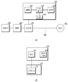
도 1은 종래기술에 의한 인버터의 전압 스트레스 조절을 위한 구조들을 나타낸 도면이다. 1 is a diagram illustrating structures for voltage stress control of an inverter according to the related art.
인버터의 전압 스트레스 조절을 위해서 도 1의 (a) 및 (b)에 도시된 바와 같이 출력선(10) 중 전동기에 가까운 측에 RC필터(12) 또는 RLC필터(14)를 설치하거나, (c) 및 (d)에 도시된 바와 같이 출력선(20) 중 인버터에 가까운 쪽에 RLC필터(22) 또는 LC필터와 클램프(CLAMP)의 조합을 설치할 수 있었다.The
이러한 경우 출력선(10, 20)의 길이가 긴 경우에 이들 필터를 장착하고, 출력선(10, 20)의 길이가 짧은 경우 이들 필터를 제거하였기 때문에 상황에 따른 구조변경이 요구되었으며, 필터를 장착할 경우 공간적 제약이 발생하였다.In this case, when the lengths of the
인버터의 전압 스트레스 조절을 위한 또 다른 방법은 도 1의 (e)와 같이 인버터의 게이트 저항(30)을 조절하는 것이다. 게이트 저항을 크게 하면 출력전압의 시간에 따른 전압변화율을 줄일 수 있다.Another method for adjusting the voltage stress of the inverter is to adjust the
게이트 저항을 도입하는 방법은 출력선의 길이가 긴 경우와 짧은 경우에 유연한 대응이 어려운 단점이 있다. 즉, 출력선의 길이가 긴 경우를 대비하여 저항을 크게하면 전압 스트레스는 줄일 수 있으나 인버터의 손실이 켜져 출력 전류를 제한시켜야 하며, 출력선의 길이가 짧은 경우를 대비하여 저항을 작게 하면 인버터의 손실은 줄일 수 있으나, 전압 스트레스가 커진다.The method of introducing a gate resistance is disadvantageous in that it is difficult to flexibly cope with a case where the length of the output line is long or short. That is, if the resistance of the output line is large, the voltage stress can be reduced, but the loss of the inverter should be turned on to limit the output current. If the resistance of the output line is made small, , But voltage stress is increased.
본 발명이 해결하고자 하는 기술적 과제는 필터나 저항 등의 추가적인 구성의 도입하지 않으면서 출력선 길이에 따른 유연한 대응이 가능한 인버터의 전압 스트레스 조절 장치를 제공하는 것이다.SUMMARY OF THE INVENTION It is an object of the present invention to provide a voltage stress control apparatus for an inverter capable of flexibly responding to the length of an output line without introducing an additional configuration such as a filter or a resistor.
상기와 같은 기술적 과제를 해결하기 위해, 본 발명의 일실시예의 인버터의 전압 스트레스 조절 장치는 인버터로부터 모터로 연결되는 출력선의 길이를 저장하는 저장부; 상기 출력선의 길이에 대응하여 인버터의 스위칭소자에 대한 구동 전압을 결정하는 인버터 제어부; 상기 결정된 구동 전압에 따라 상기 인버터의 스위칭소자의 게이트에 스위칭 전압을 제공하는 스위치모드 전압공급부;를 포함할 수 있다.According to an aspect of the present invention, there is provided an apparatus for controlling voltage stress of an inverter, including: a storage unit for storing a length of an output line connected from an inverter to a motor; An inverter control unit for determining a driving voltage for a switching element of the inverter corresponding to the length of the output line; And a switch mode voltage supplier for providing a switching voltage to the gate of the switching element of the inverter according to the determined driving voltage.
본 발명의 일실시예에서, 상기 출력선의 길이를 입력받는 입력부;를 더 포함할 수 있다.In one embodiment of the present invention, the input unit may further include an input unit receiving the length of the output line.
본 발명의 일실시예에서, 상기 스위치모드 전압공급부는 컨버터, 및 상기 컨버터를 제어하는 컨버터 제어부를 포함하고, 상기 인버터 제어부는 상기 구동전압에 상응하는 제어 신호를 상기 컨버터 제어부에 전달하고, 상기 컨버터 제어부는 상기 구동 전압에 의하여 상기 스위칭소자가 구동되도록 상기 컨버터를 제어할 수 있다.In one embodiment of the present invention, the switch mode voltage supply section includes a converter and a converter control section for controlling the converter, and the inverter control section transmits a control signal corresponding to the drive voltage to the converter control section, The control unit may control the converter to drive the switching device by the driving voltage.
.본 발명의 일실시예에서, 상기 스위치모드 전압공급부는 컨버터, 상기 컨버터 2차측에 연결된 적어도 하나 이상의 다이오드 및 상기 다이오드 각각에 병렬 연결되는 스위치를 포함할 수 있다.The switch mode voltage supply may include a converter, at least one diode connected to the converter secondary side, and a switch connected in parallel to each of the diodes.
본 발명은 RLC필터나 저항 등의 추가적인 구성을 도입하지 않아도 출력선 길이에 따른 유연한 대응이 가능한 효과가 있다.The present invention has an effect that it is possible to flexibly cope with the output line length without introducing an additional configuration such as an RLC filter or a resistor.
도 1은 종래기술에 의한 인버터의 전압 스트레스 조절을 위한 구조들을 나타낸 도면이다.
도 2는 본 발명의 일실시예에 의한 인버터의 전압 스트레스 조절 장치를 나타낸 도면이다.
도 3은 본 발명의 일실시예에 의한 인버터의 전압 스트레스 조절 장치의 적용 전과 후를 비교한 도면이다.
도 4는 본 발명의 다른 실시예에 의한 인버터의 전압 스트레스 조절 장치의 일부 구성을 나타낸 도면이다.1 is a diagram illustrating structures for voltage stress control of an inverter according to the related art.
FIG. 2 is a diagram illustrating an apparatus for controlling voltage stress of an inverter according to an embodiment of the present invention. Referring to FIG.
FIG. 3 is a graph comparing the voltage stress before and after application of the voltage stress control device of the inverter according to the embodiment of the present invention.
4 is a diagram illustrating a configuration of a voltage stress control device of an inverter according to another embodiment of the present invention.
본 발명은 다양한 변경을 가할 수 있고 여러가지 실시예를 가질 수 있는바, 특정 실시예들을 도면에 예시하고 상세한 설명에 상세하게 설명하고자 한다. 그러나, 이는 본 발명을 특정한 실시 형태에 대해 한정하려는 것이 아니며, 본 발명의 사상 및 기술범위에 포함되는 모든 변경, 균등물 내지 대체물을 포함하는 것으로 이해되어야 한다.While the invention is susceptible to various modifications and alternative forms, specific embodiments thereof are shown by way of example in the drawings and will herein be described in detail. It should be understood, however, that the invention is not intended to be limited to the particular embodiments, but includes all modifications, equivalents, and alternatives falling within the spirit and scope of the invention.
이하, 첨부된 도면을 참조하여 본 발명에 따른 바람직한 일실시예를 상세히 설명한다. Hereinafter, a preferred embodiment of the present invention will be described in detail with reference to the accompanying drawings.
도 2는 본 발명의 일실시예에 의한 인버터의 전압 스트레스 조절 장치(100)를 나타낸 도면으로서, (b)는 (a)의 인버터부(170)와 스위치모드 전압공급부(140)의 상세 구조를 나타낸 것이다. (B) shows the detailed structure of the
도 2를 참조하면 인버터는 컨버터부(150), 평활부(160), 인버터부(170), 스위치모드 전압공급부(140), 인버터 제어부(130)를 포함할 수 있다.2, the inverter may include a
컨버터부(150)는 교류전원을 직류전원으로 전환할 수 있다.The
평활부(160)는 컨버터부(150)와 연결되어 직류전원으로 전환된 전원을 평활한다.The
인버터부(170)는 평활부(160)와 연결되어 평활된 직류전원을 3상의 교류전원으로 전환하여 출력단에 제공할 수 있다. 인버터부(170)는 복수의 스위칭소자(172)를 포함할 수 있으며, 인버터부(170)의 출력전원은 출력선(180)에 의하여 전동기(200)에 전달될 수 있다.The
도 2의 (b)에서는 하나의 스위칭소자(172)가 포함되어 있는 것으로 도시되어 있으나, 이는 설명의 간단을 위해서이며, 복수의 스위칭소자(172)로 인버터부(170)가 구성되는 것임은 자명하다. 스위칭소자(172)는 예를 들어 절연 게이트 양극성 트랜지스터(IGBT)일 수 있으나, 본 발명이 이에 한정되는 것은 아니다. 2B shows that one
스위치모드 전압공급부(Switched-Mode Power Supply, SMPS)(140)는 인버터부(170)의 스위칭소자(172)의 게이트에 전원을 제공할 수 있고, 인버터 제어부(130)는 스위칭소자(172)의 스위칭 동작 등을 제어할 수 있다.The switched-mode power supply (SMPS) 140 may provide power to the gate of the
본 발명의 일실시예에 의한 인버터의 전압 스트레스 조절 장치(100)는 입력부(110), 저장부(120), 인버터 제어부(130), 스위치모드 전압공급부(140)를 포함한다.The apparatus for controlling voltage stress of an
입력부(110)는 출력선(180)의 길이를 입력 받을 수 있다. 입력부(110)는 출력선(180)의 길이를 입력받기 위하여 키패드(keypad)와 같은 사용자 인터페이스(User Interface)로 구성될 수 있다.The
입력부(110)는 출력선(180)에 대한 참고 길이와 참고 길이에 대응하는 참고 구동 전압 적어도 하나 이상 입력 받을 수도 있다.The
저장부(120)는 입력된 출력선(180)의 길이를 저장할 수 있다. 저장부(120)는 저장된 출력선(180)의 길이를 인버터 제어부(130)에 제공할 수 있다.The
저장부(120)는 또한 출력선(180)에 대한 참고 길이와 이에 대응하는 참고 구동 전압을 적어도 하나 이상 저장할 수 있다.The
인버터 제어부(130)는 입력된 또는 저장된 출력선(180)의 길이에 대응하여 인버터부(170)의 스위칭소자(172)의 게이트에 대한 구동 전압을 결정할 수 있다.The
인버터 제어부(130)는 출력선(180)의 길이가 상대적으로 긴 경우에 구동 전압을 상대적으로 낮게 결정할 수 있고, 출력선(180)의 길이가 상대적으로 짧은 경우에 구동 전압을 상대적으로 높게 결정할 수 있다.The
인버터 제어부(130)는 출력선(180)의 길이와 참고 길이 중 어느 하나를 비교하고 참고 구동 전압에 의하여 구동 전압을 결정할 수 있다. 예를 들어, 참고 길이 A(m)에 해당하는 참고 구동 전압이 a(V)이고, 참고 길이 B(m)에 해당하는 참고 구동 전압이 b(V)이고, 참고 길이 C(m)에 해당하는 참고 구동 전압이 c(V)이고, 입력된 출력선(180)의 길이가 X(m)가 X < A 인 경우 a(V)로 구동 전압을 결정하고, A ≤≤ X < B 인 경우 b(V)로 구동 전압을 결정하고, B ≤≤ X < C 인 경우 c(V)로 구동 전압을 결정할 수 있다. 또한, 인버터 제어부(130)는 구동 전압을 입력된 출력선(180)의 길이와 참고 길이와의 비율을 참고 구동 전압에 적용하여 구동 전압을 결정할 수도 있을 것이다.The
인버터 제어부(130)는 구동 전압을 결정하고, 구동 전압에 대응하는 제어 신호를 스위치모드 전압공급부(140)의 컨버터 제어부(144)에 전달할 수 있다.The
스위치모드 전압공급부(140)는 인버터 제어부(130) 및 인버터부(170)와 연결되며, 결정된 구동 전압에 따라 인버터의 스위칭소자(172)에 스위칭 전압을 제공할 수 있다.The switch mode
스위치모드 전압공급부(140)은 컨버터(142) 및 컨버터 제어부(144)를 포함할 수 있다.The switch
컨버터(142)는 컨버터 제어부(144)와 연결되며 특성이 변환된 전원을 스위칭소자(172)의 게이트에 공급할 수 있다.The
컨버터 제어부(144)는 컨버터(142)에 구동 전압에 대응하는 제어 신호를 전달하여 구동 전압에 의하여 스위칭소자(172)가 구동되도록 컨버터(142)를 제어할 수 있다.The
컨버터 제어부(144)는 공급받은 전원을 이용하여 컨버터(142)의 동작을 제어할 수 있다.The
컨버터 제어부(144)는 IC(Integrated Circuit) 보드로 구성될 수 있으며, 컨버터(142)로의 출력은 IC 보드로 입력되는 전압에 의하여 결정될 수 있다.The
즉, 스위치모드 전압공급부(140)에서 컨버터 제어부(144)를 이용하여 직접 출력전압을 제어할 수 있으나, 컨버터 제어부(144)의 IC 보드에 입력되는 전압을 제어하여서도 출력전압을 제어할 수 있다.That is, the switch
인버터 제어부(130)는 결정된 구동 전압에 대응하는 전압을 컨버터 제어부(144)에 제공할 수 있다. 이 경우 컨버터 제어부(144)는 인버터 제어부(130)로부터 제공받은 전압에 의하여 스위칭소자(172)를 구동하는 전압을 스위칭소자(172)의 게이트에 제공한다. 즉, 컨버터 제어부(144)의 IC 보드에 입력되는 전압이 제어됨으로서 스위칭소자(172)를 구동하는 전압이 최종적으로 제어되는 것이다.The
도 3은 본 발명의 일실시예에 의한 인버터의 전압 스트레스 조절 장치(100)의 적용 전과 후를 비교한 도면이다.FIG. 3 is a graph comparing the voltage stress before and after application of the voltage
출력선(180)의 길이가 길 경우 인버터의 전압 스트레스 조절 장치(100)는 스위칭소자(172)의 게이트에 입력되는 스위칭 전, 후 전압을 조절할 수 있다. 이 경우 스위칭을 하는 과정에서 전압의 시간에 따른 전압변화율은 감소할 수 있다.When the length of the
도 3에서 출력선(180)이 상대적으로 긴 경우에 인버터의 전압 스트레스 조절 장치(100)의 적용 전 결과는 실선, 적용한 후 결과는 점선으로 표시하였다.In FIG. 3, when the
스위칭소자(172)의 게이트 전압(Vge)은 인버터의 전압 스트레스 조절 장치(100) 적용 후 스위칭 전 전압은 높아지고, 스위칭 후 전압은 낮아지도록 조절되었다. 그 결과 스위치 온(Turn on) 시에 출력 전압(Vce)의 시간에 따른 전압변화율이 줄어든 것을 알 수 있으며, 출력전류(Ic)의 과전류도 억제되었다.The gate voltage Vge of the
다만 스위칭소자(172)의 온, 오프(Turn on, off) 시의 스위칭 손실(Eon, Eoff)은 인버터의 전압 스트레스 조절 장치(100) 적용 후 더 커진 것을 알 수 있다.It can be seen that the switching losses Eon and Eoff at turning on and off of the
인버터의 전압 스트레스 조절 장치(100)의 출력선(180)의 길이에 따른 스위칭소자(172) 구동 전압의 결정 방법은 과전압에 따른 위험과 스위칭 손실을 모두 고려하여 설정할 수 있을 것이다.The method of determining the driving voltage of the
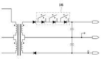
도 4는 본 발명의 다른 실시예에 의한 인버터의 전압 스트레스 조절 장치(100)의 일부 구성을 나타낸 도면이다.4 is a diagram showing a part of the configuration of an apparatus for controlling voltage stress of an inverter according to another embodiment of the present invention.
도 4를 참조하면, 스위치모드 전압공급부(140)는 스위치모드 전압공급부(140)의 컨버터(142) 2차측(2차코일 측)에 적어도 하나 이상 직렬로 연결되는 다이오드 및 다이오드에 각각 병렬로 스위치를 포함하는 조절부(146)를 더 포함할 수 있다.4, the switch mode
스위치는 인버터 제어부(130)에 의하여 열림 및 닫힘이 제어될 수 있다.The switch can be controlled to be opened and closed by the
스위치가 모두 열린 상태일 경우에 비하여 스위치가 하나 이상 닫힌 상태는 전압 강하 효과를 제공할 수 있다.If more than one switch is closed than when all switches are open, a voltage drop effect can be provided.
즉, 본 발명의 일시예에서 스위칭소자(172)의 게이트 구동 전압은 컨버터(142) 제어부로 입력되는 전압을 조절함으로써 제어될 수 있으며, 본 발명의 다른 실시예에서 스위칭소자(172) 구동 전압은 컨버터(142)의 2차측에 배치된 다이오드에 병렬연결된 스위치 상태를 제어함으로써 제어될 수 있다.That is, in the instant embodiment of the present invention, the gate driving voltage of the
이상에서 본 발명에 따른 실시예들이 설명되었으나, 이는 예시적인 것에 불과하며, 당해 분야에서 통상적 지식을 가진 자라면 이로부터 다양한 변형 및 균등한 범위의 실시예가 가능하다는 점을 이해할 것이다. 따라서, 본 발명의 진정한 기술적 보호 범위는 다음의 특허청구범위에 의해서 정해져야 할 것이다.While the invention has been shown and described with reference to certain preferred embodiments thereof, it will be understood by those skilled in the art that various changes and modifications may be made without departing from the spirit and scope of the invention as defined by the appended claims. Accordingly, the true scope of the present invention should be determined by the following claims.
100: 인버터의 전압 스트레스 조절 장치
110: 입력부
120: 저장부
130: 인버터 제어부
140: 스위치모드 전압공급부
150: 컨버터부
160: 평활부
170: 인버터부
180: 출력선
200: 전동기100: Voltage stress control device of the inverter
110: input unit
120:
130:
140: Switch mode voltage supply
150: converter section
160: Smooth part
170:
180: Output line
200: Electric motor
Claims (4)
상기 출력선의 길이에 대응하여 인버터의 스위칭소자에 대한 구동 전압을 결정하는 인버터 제어부; 및
상기 결정된 구동 전압에 따라 상기 인버터의 스위칭소자의 게이트에 스위칭 전압을 제공하는 스위치모드 전압공급부;를 포함하는 것
을 특징으로 하는 인버터의 전압 스트레스 조절 장치.
A storage unit for storing a length of an output line connected from the inverter to the motor;
An inverter control unit for determining a driving voltage for a switching element of the inverter corresponding to the length of the output line; And
And a switch mode voltage supplier for providing a switching voltage to the gate of the switching device of the inverter in accordance with the determined driving voltage
Wherein the inverter is a voltage stress regulator.
상기 출력선의 길이를 입력받는 입력부;를 더 포함하는 것
을 특징으로 하는 인버터의 전압 스트레스 조절 장치.
The method according to claim 1,
And an input unit for receiving the length of the output line
Wherein the inverter is a voltage stress regulator.
상기 스위치모드 전압공급부는 컨버터 및 상기 컨버터를 제어하는 컨버터 제어부를 포함하고,
상기 인버터 제어부는 상기 구동전압에 상응하는 제어 신호를 상기 컨버터 제어부에 전달하고,
상기 컨버터 제어부는 상기 구동 전압에 의하여 상기 스위칭소자가 구동되도록 상기 컨버터를 제어하는 것
을 특징으로 하는 인버터의 전압 스트레스 조절 장치.
The method according to claim 1,
Wherein the switch mode voltage supply unit includes a converter and a converter control unit for controlling the converter,
Wherein the inverter control unit transmits a control signal corresponding to the driving voltage to the converter control unit,
Wherein the converter control unit controls the converter so that the switching device is driven by the driving voltage
Wherein the inverter is a voltage stress regulator.
상기 스위치모드 전압공급부는 컨버터, 상기 컨버터 2차측에 연결된 적어도 하나 이상의 다이오드 및 상기 다이오드 각각에 병렬 연결되는 스위치를 포함하는 것
을 특징으로 하는 인버터의 전압 스트레스 조절 장치.
The method according to claim 1,
The switch mode voltage supply includes a converter, at least one diode connected to the converter secondary side, and a switch connected in parallel to each of the diodes
Wherein the inverter is a voltage stress regulator.
Priority Applications (1)
| Application Number | Priority Date | Filing Date | Title |
|---|---|---|---|
| KR1020170025249A KR20180098751A (en) | 2017-02-27 | 2017-02-27 | Device of adjusting voltage stress of inverter |
Applications Claiming Priority (1)
| Application Number | Priority Date | Filing Date | Title |
|---|---|---|---|
| KR1020170025249A KR20180098751A (en) | 2017-02-27 | 2017-02-27 | Device of adjusting voltage stress of inverter |
Publications (1)
| Publication Number | Publication Date |
|---|---|
| KR20180098751A true KR20180098751A (en) | 2018-09-05 |
Family
ID=63594299
Family Applications (1)
| Application Number | Title | Priority Date | Filing Date |
|---|---|---|---|
| KR1020170025249A Withdrawn KR20180098751A (en) | 2017-02-27 | 2017-02-27 | Device of adjusting voltage stress of inverter |
Country Status (1)
| Country | Link |
|---|---|
| KR (1) | KR20180098751A (en) |
-
2017
- 2017-02-27 KR KR1020170025249A patent/KR20180098751A/en not_active Withdrawn
Similar Documents
| Publication | Publication Date | Title |
|---|---|---|
| JP4844653B2 (en) | Driving device for power switching element | |
| US20160079904A1 (en) | Drive unit employing gallium nitride switches | |
| EP4113825A1 (en) | External adjustment of a drive control of a switch | |
| JP2009065485A (en) | Switching control device and motor drive device | |
| JP2016073052A (en) | Switching controller | |
| JP2009011013A (en) | Power converter | |
| CN108352776A (en) | Improved converter | |
| JP5382535B2 (en) | Power supply device for gate drive circuit | |
| JP6384316B2 (en) | Power converter and control method of power converter | |
| US8970263B2 (en) | Semiconductor device driving unit | |
| US10998887B2 (en) | Power device driving apparatus | |
| JP4135403B2 (en) | Switching circuit and power supply circuit | |
| JP4673648B2 (en) | Converter control apparatus and method, and converter and electric apparatus having the apparatus | |
| JP7099199B2 (en) | Drive circuit of the switch to be driven | |
| JP2019154134A (en) | Gate driving apparatus | |
| US20220038093A1 (en) | Gate driver | |
| KR20180098751A (en) | Device of adjusting voltage stress of inverter | |
| KR101973467B1 (en) | Power transforming apparatus having function of restraining inrush current and air conditioner including the same | |
| JP2016073051A (en) | Switching controller | |
| US10517148B2 (en) | Induction heat cooking apparatus and method for driving the same | |
| JP6969480B2 (en) | Power converter | |
| JP2012506181A (en) | Method and apparatus for reducing electromagnetic emissions during power semiconductor switch-on process | |
| JP2022092971A (en) | Drive device, semiconductor apparatus, and drive method | |
| KR101825451B1 (en) | Apparatus for controlling inverter | |
| JP2006158001A (en) | Inverter device |
Legal Events
| Date | Code | Title | Description |
|---|---|---|---|
| PA0109 | Patent application |
Patent event code: PA01091R01D Comment text: Patent Application Patent event date: 20170227 |
|
| PG1501 | Laying open of application | ||
| PC1203 | Withdrawal of no request for examination |