KR20180098343A - A single crystal layer, in particular, a method of manufacturing a piezoelectric layer - Google Patents
A single crystal layer, in particular, a method of manufacturing a piezoelectric layer Download PDFInfo
- Publication number
- KR20180098343A KR20180098343A KR1020187021267A KR20187021267A KR20180098343A KR 20180098343 A KR20180098343 A KR 20180098343A KR 1020187021267 A KR1020187021267 A KR 1020187021267A KR 20187021267 A KR20187021267 A KR 20187021267A KR 20180098343 A KR20180098343 A KR 20180098343A
- Authority
- KR
- South Korea
- Prior art keywords
- layer
- substrate
- composition
- single crystal
- donor substrate
- Prior art date
- Legal status (The legal status is an assumption and is not a legal conclusion. Google has not performed a legal analysis and makes no representation as to the accuracy of the status listed.)
- Granted
Links
Images


Classifications
-
- H—ELECTRICITY
- H10—SEMICONDUCTOR DEVICES; ELECTRIC SOLID-STATE DEVICES NOT OTHERWISE PROVIDED FOR
- H10N—ELECTRIC SOLID-STATE DEVICES NOT OTHERWISE PROVIDED FOR
- H10N30/00—Piezoelectric or electrostrictive devices
- H10N30/01—Manufacture or treatment
- H10N30/09—Forming piezoelectric or electrostrictive materials
- H10N30/093—Forming inorganic materials
-
- C—CHEMISTRY; METALLURGY
- C30—CRYSTAL GROWTH
- C30B—SINGLE-CRYSTAL GROWTH; UNIDIRECTIONAL SOLIDIFICATION OF EUTECTIC MATERIAL OR UNIDIRECTIONAL DEMIXING OF EUTECTOID MATERIAL; REFINING BY ZONE-MELTING OF MATERIAL; PRODUCTION OF A HOMOGENEOUS POLYCRYSTALLINE MATERIAL WITH DEFINED STRUCTURE; SINGLE CRYSTALS OR HOMOGENEOUS POLYCRYSTALLINE MATERIAL WITH DEFINED STRUCTURE; AFTER-TREATMENT OF SINGLE CRYSTALS OR A HOMOGENEOUS POLYCRYSTALLINE MATERIAL WITH DEFINED STRUCTURE; APPARATUS THEREFOR
- C30B25/00—Single-crystal growth by chemical reaction of reactive gases, e.g. chemical vapour-deposition growth
- C30B25/02—Epitaxial-layer growth
- C30B25/18—Epitaxial-layer growth characterised by the substrate
- C30B25/186—Epitaxial-layer growth characterised by the substrate being specially pre-treated by, e.g. chemical or physical means
-
- C—CHEMISTRY; METALLURGY
- C30—CRYSTAL GROWTH
- C30B—SINGLE-CRYSTAL GROWTH; UNIDIRECTIONAL SOLIDIFICATION OF EUTECTIC MATERIAL OR UNIDIRECTIONAL DEMIXING OF EUTECTOID MATERIAL; REFINING BY ZONE-MELTING OF MATERIAL; PRODUCTION OF A HOMOGENEOUS POLYCRYSTALLINE MATERIAL WITH DEFINED STRUCTURE; SINGLE CRYSTALS OR HOMOGENEOUS POLYCRYSTALLINE MATERIAL WITH DEFINED STRUCTURE; AFTER-TREATMENT OF SINGLE CRYSTALS OR A HOMOGENEOUS POLYCRYSTALLINE MATERIAL WITH DEFINED STRUCTURE; APPARATUS THEREFOR
- C30B25/00—Single-crystal growth by chemical reaction of reactive gases, e.g. chemical vapour-deposition growth
- C30B25/02—Epitaxial-layer growth
- C30B25/18—Epitaxial-layer growth characterised by the substrate
-
- C—CHEMISTRY; METALLURGY
- C30—CRYSTAL GROWTH
- C30B—SINGLE-CRYSTAL GROWTH; UNIDIRECTIONAL SOLIDIFICATION OF EUTECTIC MATERIAL OR UNIDIRECTIONAL DEMIXING OF EUTECTOID MATERIAL; REFINING BY ZONE-MELTING OF MATERIAL; PRODUCTION OF A HOMOGENEOUS POLYCRYSTALLINE MATERIAL WITH DEFINED STRUCTURE; SINGLE CRYSTALS OR HOMOGENEOUS POLYCRYSTALLINE MATERIAL WITH DEFINED STRUCTURE; AFTER-TREATMENT OF SINGLE CRYSTALS OR A HOMOGENEOUS POLYCRYSTALLINE MATERIAL WITH DEFINED STRUCTURE; APPARATUS THEREFOR
- C30B29/00—Single crystals or homogeneous polycrystalline material with defined structure characterised by the material or by their shape
- C30B29/10—Inorganic compounds or compositions
- C30B29/16—Oxides
- C30B29/22—Complex oxides
- C30B29/30—Niobates; Vanadates; Tantalates
-
- H01L21/02598—
-
- H01L21/76254—
-
- H01L41/047—
-
- H01L41/09—
-
- H01L41/312—
-
- H01L41/316—
-
- H01L41/319—
-
- H—ELECTRICITY
- H03—ELECTRONIC CIRCUITRY
- H03H—IMPEDANCE NETWORKS, e.g. RESONANT CIRCUITS; RESONATORS
- H03H9/00—Networks comprising electromechanical or electro-acoustic elements; Electromechanical resonators
- H03H9/02—Details
- H03H9/02007—Details of bulk acoustic wave devices
- H03H9/02015—Characteristics of piezoelectric layers, e.g. cutting angles
- H03H9/02031—Characteristics of piezoelectric layers, e.g. cutting angles consisting of ceramic
-
- H—ELECTRICITY
- H03—ELECTRONIC CIRCUITRY
- H03H—IMPEDANCE NETWORKS, e.g. RESONANT CIRCUITS; RESONATORS
- H03H9/00—Networks comprising electromechanical or electro-acoustic elements; Electromechanical resonators
- H03H9/02—Details
- H03H9/02535—Details of surface acoustic wave devices
- H03H9/02543—Characteristics of substrate, e.g. cutting angles
- H03H9/02574—Characteristics of substrate, e.g. cutting angles of combined substrates, multilayered substrates, piezoelectrical layers on not-piezoelectrical substrate
-
- H—ELECTRICITY
- H03—ELECTRONIC CIRCUITRY
- H03H—IMPEDANCE NETWORKS, e.g. RESONANT CIRCUITS; RESONATORS
- H03H9/00—Networks comprising electromechanical or electro-acoustic elements; Electromechanical resonators
- H03H9/46—Filters
- H03H9/54—Filters comprising resonators of piezoelectric or electrostrictive material
-
- H—ELECTRICITY
- H03—ELECTRONIC CIRCUITRY
- H03H—IMPEDANCE NETWORKS, e.g. RESONANT CIRCUITS; RESONATORS
- H03H9/00—Networks comprising electromechanical or electro-acoustic elements; Electromechanical resonators
- H03H9/46—Filters
- H03H9/64—Filters using surface acoustic waves
-
- H—ELECTRICITY
- H10—SEMICONDUCTOR DEVICES; ELECTRIC SOLID-STATE DEVICES NOT OTHERWISE PROVIDED FOR
- H10N—ELECTRIC SOLID-STATE DEVICES NOT OTHERWISE PROVIDED FOR
- H10N30/00—Piezoelectric or electrostrictive devices
- H10N30/01—Manufacture or treatment
- H10N30/07—Forming of piezoelectric or electrostrictive parts or bodies on an electrical element or another base
- H10N30/072—Forming of piezoelectric or electrostrictive parts or bodies on an electrical element or another base by laminating or bonding of piezoelectric or electrostrictive bodies
-
- H—ELECTRICITY
- H10—SEMICONDUCTOR DEVICES; ELECTRIC SOLID-STATE DEVICES NOT OTHERWISE PROVIDED FOR
- H10N—ELECTRIC SOLID-STATE DEVICES NOT OTHERWISE PROVIDED FOR
- H10N30/00—Piezoelectric or electrostrictive devices
- H10N30/01—Manufacture or treatment
- H10N30/07—Forming of piezoelectric or electrostrictive parts or bodies on an electrical element or another base
- H10N30/074—Forming of piezoelectric or electrostrictive parts or bodies on an electrical element or another base by depositing piezoelectric or electrostrictive layers, e.g. aerosol or screen printing
- H10N30/076—Forming of piezoelectric or electrostrictive parts or bodies on an electrical element or another base by depositing piezoelectric or electrostrictive layers, e.g. aerosol or screen printing by vapour phase deposition
-
- H—ELECTRICITY
- H10—SEMICONDUCTOR DEVICES; ELECTRIC SOLID-STATE DEVICES NOT OTHERWISE PROVIDED FOR
- H10N—ELECTRIC SOLID-STATE DEVICES NOT OTHERWISE PROVIDED FOR
- H10N30/00—Piezoelectric or electrostrictive devices
- H10N30/01—Manufacture or treatment
- H10N30/07—Forming of piezoelectric or electrostrictive parts or bodies on an electrical element or another base
- H10N30/074—Forming of piezoelectric or electrostrictive parts or bodies on an electrical element or another base by depositing piezoelectric or electrostrictive layers, e.g. aerosol or screen printing
- H10N30/079—Forming of piezoelectric or electrostrictive parts or bodies on an electrical element or another base by depositing piezoelectric or electrostrictive layers, e.g. aerosol or screen printing using intermediate layers, e.g. for growth control
-
- H—ELECTRICITY
- H10—SEMICONDUCTOR DEVICES; ELECTRIC SOLID-STATE DEVICES NOT OTHERWISE PROVIDED FOR
- H10N—ELECTRIC SOLID-STATE DEVICES NOT OTHERWISE PROVIDED FOR
- H10N30/00—Piezoelectric or electrostrictive devices
- H10N30/20—Piezoelectric or electrostrictive devices with electrical input and mechanical output, e.g. functioning as actuators or vibrators
-
- H—ELECTRICITY
- H10—SEMICONDUCTOR DEVICES; ELECTRIC SOLID-STATE DEVICES NOT OTHERWISE PROVIDED FOR
- H10N—ELECTRIC SOLID-STATE DEVICES NOT OTHERWISE PROVIDED FOR
- H10N30/00—Piezoelectric or electrostrictive devices
- H10N30/80—Constructional details
- H10N30/85—Piezoelectric or electrostrictive active materials
- H10N30/853—Ceramic compositions
- H10N30/8542—Alkali metal based oxides, e.g. lithium, sodium or potassium niobates
-
- H—ELECTRICITY
- H10—SEMICONDUCTOR DEVICES; ELECTRIC SOLID-STATE DEVICES NOT OTHERWISE PROVIDED FOR
- H10N—ELECTRIC SOLID-STATE DEVICES NOT OTHERWISE PROVIDED FOR
- H10N30/00—Piezoelectric or electrostrictive devices
- H10N30/80—Constructional details
- H10N30/87—Electrodes or interconnections, e.g. leads or terminals
-
- H—ELECTRICITY
- H10—SEMICONDUCTOR DEVICES; ELECTRIC SOLID-STATE DEVICES NOT OTHERWISE PROVIDED FOR
- H10P—GENERIC PROCESSES OR APPARATUS FOR THE MANUFACTURE OR TREATMENT OF DEVICES COVERED BY CLASS H10
- H10P14/00—Formation of materials, e.g. in the shape of layers or pillars
- H10P14/20—Formation of materials, e.g. in the shape of layers or pillars of semiconductor materials
- H10P14/34—Deposited materials, e.g. layers
- H10P14/3451—Structure
- H10P14/3452—Microstructure
- H10P14/3458—Monocrystalline
-
- H—ELECTRICITY
- H10—SEMICONDUCTOR DEVICES; ELECTRIC SOLID-STATE DEVICES NOT OTHERWISE PROVIDED FOR
- H10P—GENERIC PROCESSES OR APPARATUS FOR THE MANUFACTURE OR TREATMENT OF DEVICES COVERED BY CLASS H10
- H10P90/00—Preparation of wafers not covered by a single main group of this subclass, e.g. wafer reinforcement
- H10P90/19—Preparing inhomogeneous wafers
- H10P90/1904—Preparing vertically inhomogeneous wafers
- H10P90/1906—Preparing SOI wafers
- H10P90/1914—Preparing SOI wafers using bonding
- H10P90/1916—Preparing SOI wafers using bonding with separation or delamination along an ion implanted layer, e.g. Smart-cut
-
- H—ELECTRICITY
- H10—SEMICONDUCTOR DEVICES; ELECTRIC SOLID-STATE DEVICES NOT OTHERWISE PROVIDED FOR
- H10W—GENERIC PACKAGES, INTERCONNECTIONS, CONNECTORS OR OTHER CONSTRUCTIONAL DETAILS OF DEVICES COVERED BY CLASS H10
- H10W10/00—Isolation regions in semiconductor bodies between components of integrated devices
- H10W10/10—Isolation regions comprising dielectric materials
- H10W10/181—Semiconductor-on-insulator [SOI] isolation regions, e.g. buried oxide regions of SOI wafers
-
- C—CHEMISTRY; METALLURGY
- C01—INORGANIC CHEMISTRY
- C01G—COMPOUNDS CONTAINING METALS NOT COVERED BY SUBCLASSES C01D OR C01F
- C01G31/00—Compounds of vanadium
- C01G31/02—Oxides
-
- C—CHEMISTRY; METALLURGY
- C01—INORGANIC CHEMISTRY
- C01G—COMPOUNDS CONTAINING METALS NOT COVERED BY SUBCLASSES C01D OR C01F
- C01G33/00—Compounds of niobium
-
- C—CHEMISTRY; METALLURGY
- C01—INORGANIC CHEMISTRY
- C01G—COMPOUNDS CONTAINING METALS NOT COVERED BY SUBCLASSES C01D OR C01F
- C01G35/00—Compounds of tantalum
Landscapes
- Chemical & Material Sciences (AREA)
- Engineering & Computer Science (AREA)
- Materials Engineering (AREA)
- Crystallography & Structural Chemistry (AREA)
- Metallurgy (AREA)
- Organic Chemistry (AREA)
- Manufacturing & Machinery (AREA)
- Inorganic Chemistry (AREA)
- Acoustics & Sound (AREA)
- Physics & Mathematics (AREA)
- Ceramic Engineering (AREA)
- Chemical Kinetics & Catalysis (AREA)
- General Chemical & Material Sciences (AREA)
- Surface Acoustic Wave Elements And Circuit Networks Thereof (AREA)
- Crystals, And After-Treatments Of Crystals (AREA)
- Piezo-Electric Or Mechanical Vibrators, Or Delay Or Filter Circuits (AREA)
- Silicates, Zeolites, And Molecular Sieves (AREA)
Abstract
본 발명은 단결정 층(10)의 제조 방법에 관한 것으로, 조성 ABO3의 압전 물질을 포함하는 도너 기판(100)을 제공하는 단계로서, 여기서 A는 Li, Na, K, H 중의 적어도 하나의 원소로 구성되며, B는 Nb, Ta, Sb, V 중의 적어도 하나의 원소로 구성되는, 상기 제공하는 단계; 리시버 기판(110)을 공급하는 단계; 상기 리시버 기판 상에 상기 도너 기판을 결합시킴으로써 상기 리시버 기판(110) 상으로 상기 도너 기판(100)으로부터 "씨드층"이라 지칭되는 층(102)을 전사하는 단계로서, 상기 씨드층(102)은 결합 계면에 있게 하며, 상기 씨드층(102)까지 상기 도너 기판(100)의 박막화(thinning)가 이어지는, 상기 전사하는 단계; 상기 씨드층(102)의 압전 물질 ABO3 상에 에피택시에 의해 조성 A'B'O3의 단결정층(103)을 성장시키는 단계로서, 여기서 A'는 다음 원소들 Li, Na, K, H 중의 적어도 하나로 구성되며, B'는 다음 원소들 Nb, Ta, Sb, V 중의 적어도 하나로 구성되며, A'는 A와 다르거나 또는 B'는 B와 다른, 상기 성장시키는 단계;를 연속적으로 포함하는 것을 특징으로 한다.The present invention relates to a method of making a monocrystalline layer (10), comprising the steps of providing a donor substrate (100) comprising a piezoelectric material of composition ABO 3 , wherein A is at least one element of Li, Na, And B is composed of at least one element of Nb, Ta, Sb and V; Supplying a receiver substrate (110); Transferring a layer 102 referred to as a " seed layer " from the donor substrate 100 onto the receiver substrate 110 by coupling the donor substrate onto the receiver substrate, Wherein the donor substrate (100) is at a bonding interface and thinning of the donor substrate (100) to the seed layer (102) is performed; Growing a monocrystalline layer 103 of the composition A'B'O 3 by epitaxy on the piezoelectric material ABO 3 of the seed layer 102 wherein A 'is at least one of the following elements Li, Na, K, H And B 'is composed of at least one of the following elements Nb, Ta, Sb, V, wherein A' is different from A or B 'is different from B, .
Description
본 발명은 특히 마이크로전자, 광자, 광학 장치에 대한 응용을 위한, 단결정층, 특히 압전층을 제조하는 방법에 관한 것이다. 특히,그러나 제한적이지는 않지만, 상기 장치는 표면 음향파 장치, 또는 무선 주파수 응용을 위한 벌크 음향파 장치일 수 있다. The present invention relates to a method for manufacturing a single crystal layer, particularly a piezoelectric layer, for application to microelectronics, photons, and optical devices. In particular, but not exclusively, the device may be a surface acoustic wave device, or a bulk acoustic wave device for radio frequency applications.
무선 주파수 필드에서 필터링에 사용되는 음향 구성요소들 중에 필터의 두 가지 주요 범주들은 아래와 같이 구분될 수 있다:Among the acoustic components used for filtering in the radio frequency field, the two main categories of filters can be distinguished as follows:
첫째, 두문자로 SAW(Surface Acoustic Wave)로 알려진 표면 음향파 필터들;First, surface acoustical wave filters known as surface acoustic wave (SAW) in acronym;
둘째, 두문자로 BAW(Bulk Acoustic Wave)로 알려진 벌크 음향파 필터들 및 공명기들.Second, bulk acoustical wave filters and resonators known as BAW (Bulk Acoustic Wave) in acronyms.
이러한 기술들에 대한 검토를 위해서, W. Steichen과 S. Ballandras의 논문, "필터링에 사용되는 음향 구성 요소들 - 상이한 기술들의 검토", Techniques de l'Ingenieur [Engineering Technology], E2000, 2008[1]이 참조가 될 수 있다.For a review of these techniques, see W. Steichen and S. Ballandras, "Acoustic Components Used in Filtering-Review of Different Techniques", Techniques de l'Ingenieur [Engineering Technology], E2000, 2008 [1 ] Can be a reference.
표면 음향파 필터들은 전형적으로 두꺼운 압전층(일반적으로 수백 ㎛ 두께) 및 상기 압전층의 표면 상에 퇴적된 상호 맞물린 금속 빗들의 형태의 두 개의 전극들을 포함한다. 전극에 인가되는 전기적 신호는, 전형적으로 전압 변화는, 탄성파로 변환되고, 이것은 상기 압전층의 표면 상으로 전파된다. 이 탄성파의 전파는 파동의 주파수가 필터의 주파수 대역과 동일하면 촉진된다. 이 파동은 다른 전극에 도달하면 다시 한 번 전기 신호로 변환된다.Surface acoustic wave filters typically include two electrodes in the form of a thick piezoelectric layer (typically a few hundred micrometers thick) and intermeshing metal combs deposited on the surface of the piezoelectric layer. The electrical signal applied to the electrode is typically converted into an acoustic wave, which is propagated on the surface of the piezoelectric layer. Propagation of this elastic wave is promoted when the frequency of the wave is the same as the frequency band of the filter. This wave is once again converted to an electrical signal when it reaches the other electrode.
그들의 부분에서, 벌크 음향파 필터들은 전형적으로 얇은 압전층(즉, 대체로 대략 1㎛ 미만의 두께) 및 상기 얇은 층의 각각의 주 표면 상에 설치된 2개의 전극들을 포함한다. 전극에 인가되는 전기적 신호는, 전형적으로 전압 변화는 탄성파로 변환되어 압전층을 통해 전파된다. 이 탄성파의 전파는 파동의 주파수가 필터의 주파수 대역과 동일하면 촉진된다. 이 파동은 반대쪽 면의 전극에 도달하면 다시 한 번 전기 신호로 변환된다.In their portion, the bulk acoustic wave filters typically comprise a thin piezoelectric layer (i.e., generally less than about 1 탆 thick) and two electrodes mounted on each major surface of the thin layer. The electrical signal applied to the electrode is typically converted into an elastic wave and propagated through the piezoelectric layer. Propagation of this elastic wave is promoted when the frequency of the wave is the same as the frequency band of the filter. This wave is once again converted into an electric signal when it reaches the electrode on the opposite side.
표면 음향파 필터들의 경우, 압전층은 표면파의 어떠한 감쇠를 야기시키지 않기 위해 우수한 결정질이어야 한다. 이 경우 단결정층이 따라서 바람직할 것이다. 현재, 산업적으로 사용될 수 있는 적합한 재료들은 석영, LiNbO3 또는 LiTaO3이다. 압전층은 상기 재료들 중 하나의 잉곳(ingot)을 절단함으로써 얻어지며, 여기서 상기 층의 두께에 요구되는 정확도는 상기 파동들이 본질적으로 그것의 표면상에서 전파되는 경우라면 중요하지 않다.In the case of surface acoustic wave filters, the piezoelectric layer must be of good crystalline to avoid any attenuation of surface waves. In this case, a monocrystalline layer is therefore preferable. Currently, suitable materials which can be used industrially are quartz, LiNbO 3 or LiTaO 3. The piezoelectric layer is obtained by cutting one ingot of the materials, where the required accuracy of the thickness of the layer is not critical if the waves propagate essentially on its surface.
벌크 음향파 필터들의 경우, 압전층은 정밀하게 제어된 방식으로 전체 층에 걸쳐 단단하고 균일한 두께를 가져야 한다. 반대로, 결정 품질은 필터의 성능에 대한 중요한 기준의 관점에서 이차적이기 때문에, 상기 층의 결정 품질에 관해서는 현재 절충들이 이루어지고 있으며, 그리고 다결정층은 오랫동안 수용 가능한 것으로 간주되어 왔다. 따라서, 압전층은 지지 기판(예를 들어, 실리콘 기판) 상에 퇴적됨으로써 형성된다. 현재 이러한 퇴적을 위해 산업적으로 사용되는 물질들은 AlN, ZnO 및 Pb(ZrX, Ti1-X)O3(PZT)이다.In the case of bulk acoustic wave filters, the piezoelectric layer must have a hard and uniform thickness over the entire layer in a precisely controlled manner. Conversely, since crystal quality is secondary in terms of important criteria for the performance of the filter, current compromises have been made with respect to the crystal quality of the layer, and polycrystalline layers have long been regarded as acceptable. Therefore, the piezoelectric layer is formed by being deposited on a supporting substrate (for example, a silicon substrate). Is the current material to be industrially used for this deposition are AlN, ZnO and Pb (Zr X, Ti 1- X) O 3 (PZT).
따라서 재료들의 선택은 양쪽 기술들에서 매우 제한적이다.Thus, the choice of materials is very limited in both technologies.
그러나 재료의 선택은 필터 제조업체의 사양에 따라 필터의 상이한 속성들 간의 절충의 결과이다. 특히, 압전 재료들의 전기기계 결합 계수는 주어진 적용 및 주어진 구성 요소 아키텍처에 사용해야 하는 재료의 선택에 대한 기준이다.However, the choice of material is the result of compromises between the different properties of the filter according to the specifications of the filter manufacturer. In particular, the electromechanical coupling factor of piezoelectric materials is a criterion for the choice of materials to be used for a given application and a given component architecture.
예를 들어, LiNbO3 및 LiTaO3는 고도의 이방성 물질들이다. 상기 결합 계수는 결정 배향에 의존하기 때문에, 재료의 특정 배향의 선택은 재료의 선택을 위한 제1 자유도를 제공한다. 이것이 기판들이 예를 들어, X-컷, Y-컷, Z-컷, YZ-컷, 36°회전된 Y 축, 42°회전된 Y 축 등과 같이 다수의 결정 배향들과 함께 찾아질 수 있는 이유이다.For example, LiNbO 3 and LiTaO 3 are the anisotropic material of the altitude. Since the coupling coefficient depends on the crystal orientation, the selection of a particular orientation of the material provides a first degree of freedom for selection of the material. This is the reason why substrates can be found with a large number of crystal orientations such as, for example, X-cut, Y-cut, Z-cut, YZ-cut, 36 ° rotated Y axis, 42 ° rotated Y axis, to be.
그러나, 특정한 결정 배향을 선택할 수 있다는 사실을 제외하고, 예를 들어, 랑가사이트(langasite) La3Ga5SiO14와 같이 이 목록에 몇 가지 다른 재료들이 미래에 추가 될지라도, 당업자는 필터의 특성을 최적화하기 위한 제한된 범위의 파라미터들만을 제공하면서, 표면 음향파 필터를 설계하기 위해 단지 석영, LiNbO3 및 LiTaO3만을 가진다.However, even if several other materials are added to this list in the future, such as, for example, langasite La 3 Ga 5 SiO 14 , except for the fact that a particular crystal orientation can be chosen, only it has only quartz, LiNbO 3 and LiTaO 3, while providing only a limited range of the parameters, in order to design a surface acoustic wave filter for optimizing.
벌크 음향파 필터들 또는 표면 음향파 필터들의 치수를 더욱 자유롭게 하기 위해, 재료들의 품질이 손상되지 않는다면 위에 열거된 재료들보다 많은 재료들을 사용할 수 있는 것이 바람직하다.In order to further free the dimensions of the bulk acoustic wave filters or surface acoustic wave filters, it is desirable to be able to use more materials than those listed above, provided that the quality of the materials is not compromised.
본 발명의 목적 중 하나는 전술한 단점들을 개선하기 위한 것이고, 특히 표면 음향파 장치들을 위해 사용된 재료들로 만들어지며, 층들을 얇고(즉, 20 ㎛ 미만 두께, 또는 1 ㎛ 미만 두께) 균질하게 얻어질 수 있게 함으로써, 본 응용에서 사용된 재료들 이외의 재료들로 제조된, 특히 표면 음향파 장치를 위한, 단결정 층, 특히 압전층을 제조하는 방법을 고안하는 것이다. 이 방법은 또한 기존의 벌크 음향파 장치에서보다 더 다양한 종류의 지지 기판들을 사용할 수 있어야 한다.One of the objects of the present invention is to improve the above-mentioned disadvantages, and in particular to make the layers thinner (i.e. less than 20 탆 thick, or less than 1 탆 thick) homogeneous Especially a surface acoustic wave device, made of materials other than those used in the present application by making it possible to obtain a monocrystalline layer, in particular a piezoelectric layer. This method should also be able to use a larger variety of support substrates than conventional bulk acoustic wave devices.
본 발명에 따라서, 단결정 층의 제조 방법이 제안되었으며, 이것은 다음의 연속적인 단계들을 포함하는 것을 특징으로 한다: According to the present invention, a method of producing a monocrystalline layer has been proposed, which is characterized in that it comprises the following successive steps:
- 조성 ABO3의 압전 물질을 포함하는 도너 기판을 제공하는 단계로서, 여기서 A는 Li, Na, K, H 중의 적어도 하나의 원소로 구성되며, B는 Nb, Ta, Sb, V 중의 적어도 하나의 원소로 구성되는, 상기 제공하는 단계;- providing a donor substrate comprising a piezoelectric material of composition ABO 3 wherein A comprises at least one element of Li, Na, K, H and B is at least one of Nb, Ta, Sb, V Element;
- 리시버 기판을 공급하는 단계;Feeding the receiver substrate;
- 상기 리시버 기판 상에 상기 도너 기판을 결합시킴으로써 상기 리시버 기판 상으로 상기 도너 기판으로부터 "씨드층"이라 지칭되는 층을 전사하는 단계로서, 상기 씨드층은 결합 계면에 있게 하며, 상기 씨드층까지 상기 도너 기판의 박막화(thinning)가 이어지는, 상기 전사하는 단계;Transferring a layer referred to as a " seed layer " from the donor substrate onto the receiver substrate by engaging the donor substrate on the receiver substrate, the seed layer being at the bonding interface, Followed by thinning of the donor substrate;
- 상기 씨드층의 압전 물질 ABO3 상에 에피택시에 의해 조성 A'B'O3의 단결정층을 성장시키는 단계로서, 여기서 A'는 다음 원소들 Li, Na, K, H 중의 적어도 하나로 구성되며, B'는 다음 원소들 Nb, Ta, Sb, V 중의 적어도 하나로 구성되며, A'는 A와 다르거나 또는 B'는 B와 다른, 상기 성장시키는 단계.- growing a monocrystalline layer of composition A'B'O 3 by epitaxy on the piezoelectric material ABO 3 of the seed layer, wherein A 'consists of at least one of the following elements Li, Na, K, H , B 'consists of at least one of the following elements Nb, Ta, Sb, V, wherein A' is different from A or B 'is different from B.
"상기 결합 계면에서의 층"이라는 표현은 제2 기판에 결합된 제1 기판의 면측상의 층을 의미하는 것으로 이해되지만, 상기 층과 상기 제2 기판 사이에 직접 접촉이 있음을 반드시 함의하는 것은 아니다. 따라서, 상기 층은 상기 제2 기판에 직접 결합될 수 있거나 또는 상기 결합이 수행되는 결합 층, 예를 들어 유전체층 또는 임의의 다른 유형의 층에 의해 덮일 수도 있다.The expression " layer at the bonding interface " is understood to mean a layer on the side of the first substrate bonded to the second substrate, but does not necessarily mean that there is a direct contact between the layer and the second substrate . Thus, the layer may be directly bonded to the second substrate, or it may be covered by a bonding layer, for example a dielectric layer or any other type of layer on which the bonding is performed.
"A는 A'와 상이하다"라는 표현은 A와 A'가 상이한 원소들로 구성되는, 및/또는 동일한 원소(들)이지만 상이한 화학양론적 비율로 구성되는 것을 의미하는 것으로 이해할 수 있다.The expression " A is different from A '" can be understood to mean that A and A' are composed of different elements and / or are the same element (s), but composed of different stoichiometric ratios.
하나의 실시 예에 따라, A'는 A와 마찬가지로 적어도 하나의 원소를 포함하며, 및/또는 B'는 B와 마찬가지로 적어도 하나의 원소를 포함할 수 있다.According to one embodiment, A 'comprises at least one element as in A, and / or B' may comprise at least one element as in B.
"A'는 A와 마찬가지로 적어도 하나의 원소를 포함한다"라는 표현은 주어진 원소(또는 몇가지 원소들)가 A 및 A' 양쪽에, 동일한 또는 상이한 화학양론적 비율로 존재한다는 것을 의미하는 것으로 이해될 수 있다.The expression " A ' includes at least one element as well as A " is understood to mean that a given element (or some elements) exists in both A and A 'at the same or different stoichiometric proportions .
하나의 실시 예에 따라, B'가 B와 상이할 경우 A'는 A와 동일하며, 그리고 A'가 A와 상이할 경우 B'는 B와 동일할 수 있다. According to one embodiment, A 'is equal to A when B' is different from B, and B 'may be equal to B if A' is different from A.
"A는 A'와 동일하다"라는 표현은 A'와 A가 동일한 화학양론적 비율로 동일한 원소(들)로 구성된다는 것을 의미하는 것으로 이해될 수 있다.The expression "A is the same as A '" can be understood to mean that A' and A are composed of the same element (s) in the same stoichiometric ratio.
하나의 실시 예에 따라, A는 단일 원소로 구성되며, 그리고 B도 단일 원소로 구성될 수 있다. According to one embodiment, A consists of a single element, and B can also be composed of a single element.
본 발명을 수행하는 하나의 방법에 따라, 상기 씨드층을 전사하는 단계는 다음의 단계들을 포함한다:According to one method of carrying out the invention, the step of transferring the seed layer comprises the following steps:
- 상기 조성 ABO3의 압전 물질을 포함하며, 상기 씨드층이라 지칭되는 층을 제한하도록 상기 도너 기판에 취성 영역을 형성하는 단계;Forming a brittle region in the donor substrate to limit the layer referred to as the seed layer, comprising a piezoelectric material of the composition ABO 3 ;
- 상기 씨드층이 결합 계면에 있도록, 상기 리시버 기판 상에 상기 도너 기판을 결합시키는 단계;Coupling the donor substrate onto the receiver substrate such that the seed layer is at a bonding interface;
- 상기 씨드층을 상기 리시버 기판 상으로 전사하기 위해 상기 취성 영역을 따라 상기 도너 기판을 분리하는 단계.Separating the donor substrate along the embrittlement region to transfer the seed layer onto the receiver substrate.
상기 에피택시의 단계 전에, 상기 리시버 기판 상으로 전사된 상기 씨드층의 두께의 일부가 제거될 수 있다.Before the step of epitaxy, a part of the thickness of the seed layer transferred onto the receiver substrate may be removed.
유리하게는, 상기 씨드층의 두께는 2 ㎛ 미만이며, 바람직하게는 1 ㎛ 미만일 수 있다.Advantageously, the thickness of the seed layer is less than 2 [mu] m, preferably less than 1 [mu] m.
상기 리시버 기판은 유리하게는 반도체 물질로 이루어지며, 그리고 상기 씨드층과 상기 리시버 기판 사이에 중간 전하-트랩핑 층을 포함할 수 있다.The receiver substrate is advantageously made of a semiconductor material and may include an intermediate charge-trapping layer between the seed layer and the receiver substrate.
본 발명의 다른 대상은 단결정 층의 제조 방법에 관한 것으로서, 이것은 다음의 연속적인 단계들을 포함할 수 있다:Another object of the present invention relates to a method of manufacturing a monocrystalline layer, which may include the following sequential steps:
- 조성 A'B'O3의 압전 물질을 포함하는 도너 기판을 제공하는 단계로서, 여기서 A'는 다음 원소들 Li, Na, K, H 중의 적어도 하나 이상으로 구성되며, B'는 다음 원소들 Nb, Ta, Sb, V 중의 적어도 하나 이상으로 구성되는, 상기 제공하는 단계;Providing a donor substrate comprising a piezoelectric material of composition A'B'O 3 , wherein A 'consists of at least one of the following elements Li, Na, K, H, and B' Nb, Ta, Sb, and V;
- 상기 압전 물질 A'B'O3 상에 에피택시에 의해 조성 A''B''O3의 단결정층(103)을 성장시키는 단계로서, 여기서 A''는 다음 원소들 Li, Na, K, H 중의 하나 이상으로 구성되며, B''는 다음 원소들 Nb, Ta, Sb, V 중의 하나 이상으로 구성되는, 상기 성장시키는 단계;- growing a single crystal layer (103) of composition A "B" O 3 by epitaxy on said piezoelectric material A'B'O 3 , wherein A "comprises the following elements Li, Na, K , H, and B "comprises at least one of the following elements Nb, Ta, Sb, V;
- 리시버 기판을 공급하는 단계;Feeding the receiver substrate;
- 에피택셜 층을 통하여 상기 리시버 기판 상에 상기 도너 기판을 결합시킴으로써 상기 리시버 기판 상으로 조성 A''B''O3의 상기 에피택셜 층의 적어도 일부를 전사하는 단계로서, 조성 A''B''O3의 상기 에피택셜 층까지 상기 도너 기판의 박막화가 이어지는, 상기 전사하는 단계.Transferring at least a portion of the epitaxial layer of composition A " B " O 3 onto the receiver substrate by bonding the donor substrate onto the receiver substrate through an epitaxial layer, &Quot;"'O 3 , followed by thinning of the donor substrate to the epitaxial layer of O 3 .
하나의 실시 예에 따라, 조성 A''B''O3의 층이 상기 리시버 기판 상으로 전사된 후에, 상기 조성 A''B''O3의 물질 상에, 에피택시에 의해 조성 A'''B'''O3의 단결정 층이 성장되며, 여기서 A'''는 다음 원소들 Li, Na, K, H 중의 하나 이상으로 구성되며, B'''는 다음 원소들 Nb, Ta, Sb, V 중의 하나 이상으로 구성될 수 있다.According to one embodiment, after the layer of the composition A''B "O 3 is transferred onto the receiver substrate, on the material of the composition A" B "O 3 , by the epitaxy, the composition A ''' B '' and a single crystal layer of the 'O 3 growth, in which a''' will then be composed of elements of Li, at least one of Na, K, H, B '''has the following elements Nb, Ta, Sb, and V, respectively.
하나의 실시 예에 따라, A'''는 A''와 상이하거나 또는 B'''는 B''와 상이할 수 있다.According to one embodiment, A '' 'may be different from A' 'or B' '' may be different from B ''.
본 발명을 수행하는 하나의 방법에 따라, 상기 리시버 기판 상으로 조성 A''B''O3의 상기 에피택셜층)의 적어도 일부를 전사하는 단계는 다음 단계들을 포함할 수 있다:According to one method of carrying out the invention, the step of transferring at least a portion of the epitaxial layer of composition A " B " O 3 onto the receiver substrate may comprise the following steps:
- 전사되어지는 층을 제한하기 위해, 상기 도너 기판 내에 또는 조성 A''B''O3의 상기 에피택셜층 내에 취성 영역을 형성하는 단계;Comprising the steps of, forming an embrittlement zone in the epitaxial substrate of the donor in the composition or A''B''O layer 3 to restrict the layer which is transferred;
- 조성 A''B''O3의 상기 에피택셜층이 결합 계면에 있도록, 상기 리시버 기판 상에 상기 도너 기판을 결합시키는 단계;Bonding the donor substrate on the receiver substrate such that the epitaxial layer of composition A " B " O 3 is at the bonding interface;
- 상기 취성 영역을 따라 상기 도너 기판 또는 상기 에피택셜층을 분리하는 단계.Separating the donor substrate or the epitaxial layer along the embrittlement zone.
하나의 실시 예에 따라, 상기 취성 영역은 상기 도너 기판 내에 형성되며, 상기 전사하는 단계 후에, 전사된 상기 층은 조성 A''B''O3의 물질을 노출시키도록 박막화될 수 있다.According to one embodiment, the embrittlement zone is formed in the donor substrate, after the step of the transfer, the transferred layer can be made thin so as to expose the material of the composition A''B''O 3.
하나의 실시 예에 따라, A''는 A'와 상이하거나 또는 B''는 B'와 상이할 수 있다.According to one embodiment, A "may be different from A 'or B" may be different from B'.
하나의 실시 예에 따라, A''는 A'와 마찬가지로 적어도 하나의 원소를 포함하며, 및/또는 B''는 B'와 마찬가지로 적어도 하나의 원소를 포함할 수 있다.According to one embodiment, A '' comprises at least one element as well as A 'and / or B' 'may comprise at least one element as well as B'.
하나의 실시 예에 따라, B''가 B'와 상이할 경우 A''는 A'와 동일하며, 그리고 A''가 A'와 상이할 경우 B''는 B'와 동일할 수 있다.According to one embodiment, A "is the same as A 'when B" is different from B', and B "may be the same as B 'when A" is different from A'.
하나의 실시 예에 따라, A'는 단일 원소로 구성되며, 그리고 B'도 단일 원소로 구성될 수 있다.According to one embodiment, A 'consists of a single element, and B' can also be composed of a single element.
하나의 실시 예에 따라, 상기 취성 영역은 상기 도너 기판 내에 이온 주입에 의해 형성될 수 있다.According to one embodiment, the brittle region may be formed by ion implantation in the donor substrate.
특히 유리한 방식에서, 에피택시 단계 후에, 조성 A''B''O3의 단결정 층의 두께는 0.2 내지 20 ㎛ 일 수 있다.In a particularly advantageous manner, after the epitaxy step, the thickness of the monocrystalline layer of composition A " B " O 3 may be between 0.2 and 20 μm.
부가적으로, 상기 리시버 기판과 상기 도너 기판 사이의 계면에 적어도 하나의 전기적 절연층 및/또는 적어도 하나의 전기적 도전층이 형성될 수 있다.In addition, at least one electrically insulating layer and / or at least one electrically conductive layer may be formed on the interface between the receiver substrate and the donor substrate.
본 발명을 수행하는 하나의 방법에 따라, 상기 방법은 최종 기판 상으로 상기 리시버 비판의 단결정 층의 적어도 일부를 전사시키는 단계를 포함할 수 있다.According to one method of carrying out the invention, the method may comprise transferring at least a portion of the single crystal layer of the receiver criterion onto a final substrate.
다른 대상은 마이크로일렉트로닉, 포토닉 또는 광학 장치를 위한 기판에 관한 것으로서, 이것은 지지 기판과, 상기 지지 기판 상에 조성 A''B''O3의 단결정 층으로서, 여기서 A''는 다음 원소들 Li, Na, K, H 중의 하나 이상으로 구성되며, B''는 다음 원소들 Nb, Ta, Sb, V 중의 하나 이상으로 구성되며, A'' 및 B'' 중의 적어도 하나는 적어도 두개의 원소들로 구성되는, 상기 단결정 층(103)과, 그리고 상기 지지 기판과 조성 A''B''O3의 상기 층 사이에 조성 A'B'O3의 층으로서, 여기서 A'는 다음 원소들 Li, Na, K, H 중의 적어도 하나의 원소로 구성되며, B'는 다음 원소들 Nb, Ta, Sb, V 중의 적어도 하나의 원소로 구성되는, 상기 층을 포함할 수 있다.Another object relates to a substrate for a microelectronic, photonic or optical device comprising a support substrate and a single crystal layer of composition A '' B '' O 3 on said support substrate, wherein A ' Wherein at least one of A "and B" is composed of at least one of Li, Na, K, H and B "is composed of at least one of the following elements Nb, Ta, Sb, , and the
하나의 실시 예에 따라, 상기 기판은 조성 A''B''O3의 상기 층 상에, 조성 A'''B'''O3의 단결정 층을 더 포함하며, 여기서 A'''는 다음 원소들 Li, Na, K, H 중의 하나 이상으로 구성되며, B'''는 다음 원소들 Nb, Ta, Sb, V 중의 하나 이상으로 구성될 수 있다.According to one embodiment, the substrate further comprises a layer of the composition on the A''B''O 3, composition A '''B''single-crystal layer of the' O 3, wherein A '''is It consists of one or more of the following elements Li, Na, K, H, and B '''can consist of one or more of the following elements Nb, Ta, Sb,
다른 대상은 단결정 압전층의 표면에 전극들을 퇴적하는 단계를 포함하는 표면 음향파 장치의 제조방법에 관한 것으로서, 위에 기술된 제조방법에 의하여 상기 압전층을 제조하는 것을 포함할 수 있는 것을 특징으로 한다.Another object is to manufacture a surface acoustic wave device comprising depositing electrodes on the surface of a single crystal piezoelectric layer, which can include manufacturing the piezoelectric layer by the manufacturing method described above .
다른 대상은 표면 음향파 장치에 관한 것으로서, 위에 기술된 제조 방법에 의해 얻어질 수 있는 단결정 압전층, 및 상기 단결정 압전층의 표면에 형성된 두 개의 전극들을 포함할 수 있는 것을 특징으로 한다.Another object relates to a surface acoustic wave device, which can include a single crystal piezoelectric layer obtainable by the above-described manufacturing method, and two electrodes formed on the surface of the single crystal piezoelectric layer.
본 발명의 다른 대상은 외부 응력에 의해 야기된 변형을 측정하기 위해 설계된 마이크로-센서에 관한 것으로서, 위에 기술된 제조방법에 의해 얻어질 수 있는 단결정 압전층을 포함할 수 있는 것을 특징으로 한다. Another object of the present invention is a micro-sensor designed to measure deformation caused by external stress, which is characterized in that it can comprise a single crystal piezoelectric layer obtainable by the manufacturing method described above.
본 발명의 다른 대상은 연속적 또는 가변적 전기장의 인가를 통하여, 성분의 변형 또는 이동 부분의 이동을 야기하도록 설계된 마이크로-액츄에이터에 관한 것으로서, 위에 기술된 제조방법에 의해 얻어질 수 있는 단결정 압전층을 포함하는 것을 특징으로 한다.Another object of the present invention relates to a micro-actuator designed to cause deformation of a component or movement of a moving part through the application of a continuous or variable electric field, comprising a single crystal piezoelectric layer obtainable by the above- .
본 발명의 다른 특성들 및 장점들은 첨부된 도면들을 참조하여, 아래에 주어진 상세한 설명으로부터 명백하게 보여질 것이며, 여기서,
도 1은 표면 음향파 필터의 단면 기능도이며,
도 2는 벌크 음향파 필터의 단면 기능도이며,
도 3a 내지 3e는 본 발명의 제1 실시 예에 따른 단결정 층을 제조하는 방법의 연속적인 단계들을 보여주며,
도 4a 내지 4e는 본 발명의 제2 실시 예에 따른 단결정 층을 제조하는 방법의 연속적인 단계들을 보여주며,
도 4f는 도 4a 내지 4e에 도시된 실시 예의 변형으로 구현된 부가적인 단계를 보여주며,
도 5a 내지 도 5c는 상기 단계의 선택적인 연속 단계들을 보여준다.
도면들의 판독성을 위해, 도시된 요소들은 반드시 스케일로 나타내지는 않았다. 상이한 도면들에서 동일한 참조 부호들에 의해 지시 된 요소들은 동일하다.Other features and advantages of the present invention will become apparent from the following detailed description, taken in conjunction with the accompanying drawings,
1 is a cross-sectional functional diagram of a surface acoustic wave filter,
2 is a cross-sectional functional diagram of a bulk acoustic wave filter,
3A through 3E show successive steps of a method of manufacturing a monocrystalline layer according to a first embodiment of the present invention,
Figures 4A-4E illustrate successive steps of a method of making a monocrystalline layer according to a second embodiment of the present invention,
Figure 4f shows additional steps implemented with variations of the embodiment shown in Figures 4a-4e,
Figures 5A-5C illustrate the optional successive steps of the step.
For readability of the figures, the elements shown are not necessarily drawn to scale. The elements indicated by the same reference numerals in different Figures are the same.
도 1은 표면 음향파 필터의 기능도이다.1 is a functional diagram of a surface acoustic wave filter.
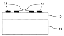
상기 필터는 압전층(10) 및 상기 압전층의 표면 상에 퇴적된 두개의 맞물린 금속 빗살의 형태로 두개의 전극들(12,13)을 포함한다. 전극들(12,13) 반대측 상에서, 상기 압전층이 지지 기판(11) 상에 놓인다. 압전층(10)은 단결정이며; 정말로 표면파에 어떠한 감쇠도 야기되지 않도록 우수한 결정 품질이 요구된다.The filter comprises a piezoelectric layer (10) and two electrodes (12, 13) in the form of two interdigitated metal batts deposited on the surface of the piezoelectric layer. On the opposite side of the
도 2는 벌크 음향파 공명기의 기능도이다.2 is a functional diagram of a bulk acoustic wave resonator.
상기 공명기는 얇은 압전층(즉, 일반적으로 1㎛ 미만의 두께, 바람직하게는 0.2㎛ 미만의 두께) 및 본 발명의 제조 방법에 기인하여, 단결정인 상기 압전층(10)의 어느 측에 설치된 두 개의 전극들(12,13)을 포함한다. 압전층(10)은 지지 기판(11) 상에 놓여있다. 상기 기판으로부터 상기 공명기를 분리하기 위해, 그리고 이 방법에 의해 상기 기판 상에서 전파되는 파동들을 방지하기 위해, 브래그 미러(Bragg mirror, 14)가 전극(13)과 기판(110 사이에 끼어있다. 대안적인 방식(도시 안됨)으로, 이러한 분리는 상기 기판과 상기 압전층 사이에 캐비티(cavity)를 만듦으로써 달성될 수 있다. 이러한 다양한 배열들을 당업자들에게 알려져 있으며, 따라서 본 명세서에서 상세하게 기술하지는 않을 것이다.The resonator is formed of a
일반적인 방식에서, 본 발명은 단결정층, 특히 압전층의 형성을 제안하며, 상기 단결정층을 위해 원하는 두께가 얻어질 때까지 에피택시를 위한 씨드로서 사용되는 도너(donor) 기판의 물질 상에 에피택시에 의해, 그리고 리시버(receiver) 기판으로의 전사(transfer)에 의해 압전층을 형성하며, 여기서 상기 전사는 상기 에피택시 전에(이 경우에, 상기 씨드층이라 지칭되는 상기 도너 기판의 표면층이 상기 리시버 기판 상으로 전사된다), 또는 에피택시 후에(이 경우에, 상기 에피택시 층의 적어도 일부가 상기 리시버 기판 상으로 전사된다) 달성될 수 있다. In a general manner, the present invention proposes the formation of a monocrystalline layer, in particular a piezoelectric layer, on which epitaxy is formed on the material of a donor substrate used as a seed for epitaxy until a desired thickness is obtained for the monocrystalline layer And the transfer to a receiver substrate, wherein the transfer is performed prior to the epitaxy (in this case, the surface layer of the donor substrate, referred to as the seed layer, Transferred onto the substrate), or after epitaxy (in which case at least a portion of the epitaxial layer is transferred onto the receiver substrate).
상기 도너 기판은 논의되고 있는 물질의 동종 단결정 기판일 수 있다. 대안적으로, 상기 도너 기판은 합성 기판, 즉 적어도 두 개의 상이한 물질 층들의 스택의 형태로, 그것의 표면층은 논의되고 있는 단결정 물질로 구성되는, 합성 기판일 수 있다.The donor substrate may be a homogeneous monocrystalline substrate of the material being discussed. Alternatively, the donor substrate can be a composite substrate, i.e. a composite substrate, in the form of a stack of at least two different material layers, the surface layer of which is composed of the single crystal material being discussed.
특히 관심을 끌고 있는 압전 재료들 중에는 ABO3 구조의 페로브스카이트들 (perovskites) 및 유사한 재료들이 있다. 그러나 이러한 재료들이 가질 수 있는 관심은 압전 특성으로 제한되지 않는다. 특히, 예를 들어 집적 광학에 관련된 응용 분야와 같은 다른 응용 분야의 경우에서, 예를 들어 적용 가능한 바와 같이, 그들의 유전율, 굴절 지수, 또는 대안적으로 그들의 초전성, 강유전성 또는 대안적으로 강자성 특성들로 인해 관심 대상이 될 수 있다.Among the piezoelectric materials of particular interest are perovskites of the ABO 3 structure and similar materials. However, interest that these materials may have is not limited to piezoelectric properties. In particular, in the case of other applications, for example applications related to integrated optics, their permittivity, refractive index, or alternatively their superconducting, ferroelectric or, alternatively, ferromagnetic properties, such as, for example, Can be of interest.
큰 계열이 드러난다. 이것은 LiNbO3, LiTaO3, KNbO3, KTaO3와 같은 이원 재료들로부터 특히 유도되며, ABO3 유형의 일반 화학식을 유도되며, 여기서 A는 다음 원소들 Li, Na, K, H 중의 하나 이상의 원소로 구성되며, B는 다음 원소들 Nb, Ta, Sb, V 중의 하나 이상의 원소로 구성된다.A large series is revealed. It is derived specifically from binary materials such as LiNbO 3 , LiTaO 3 , KNbO 3 and KTaO 3 and is derived from a general formula of type ABO 3 , where A is one or more of the following elements Li, Na, K, And B is composed of at least one of the following elements Nb, Ta, Sb, V:
요약하면, A는 다음 원소들 Li, Na, K, H 중의 하나 이상으로 구성되며, B는 다음 원소들 Nb, Ta, Sb, V 중의 하나 이상으로 구성된다고 생각될 것이다.In summary, it is assumed that A consists of one or more of the following elements Li, Na, K, H and B consists of one or more of the following elements Nb, Ta, Sb,
상기 리시버 기판은 상기 씨드층의 기계적 지지대로서 역할을 한다. 이것은 에피택시의 구현에 적합한(특히 고온에서의 성능의 안정성 면에서), 그리고 유리하게도, 부득이한 것은 아니지만, 논의되는 응용에서 적합한 어떠한 종류일 수 있다. 이것은 동종적 또는 합성적일 수 있다.The receiver substrate serves as a mechanical support for the seed layer. This may be any kind suitable for the application being discussed, which is suitable for the implementation of the epitaxy (especially in terms of performance stability at high temperatures) and advantageously, although not necessarily. It may be homogeneous or synthetic.
적어도 하나의 중간층이 상기 리시버 기판과 상기 씨드층 사이에 삽입될 수 있다. 예를 들어, 이러한 중간층은 전기적으로 도전성이거나 또는 전기적으로 절연성일 수 있다. 통상의 기술자는 상기 압전층을 포함하고자 하는 상기 고주파수 장치가 갖기를 바라는 특성들에 따라 상기 층의 재료 및 두께를 선택할 수 있을 것이다.At least one intermediate layer may be interposed between the receiver substrate and the seed layer. For example, the intermediate layer may be electrically conductive or electrically insulating. A person skilled in the art will be able to select the material and thickness of the layer in accordance with the desired properties of the high frequency device intended to contain the piezoelectric layer.
유리하게는, 상기 리시버 기판은 반도체 재료로 제조될 수 있다. 예를 들어, 이것은 실리콘 기판일 수 있다. 이 도전성 재료는 "트랩-리치(trap-rich)" 타입의 중간층을 포함하며, 이것은 상기 리시버 기판 상에 형성되거나 또는 상기 리시버 기판의 표면 상에 형성되거나 어느 하나일 수 있다. 상기 트랩-리치 타입의 상기 중간층은 따라서 상기 씨드층과 상기 리시버 기판 사이에 위치되며, 그리고 상기 리시버 기판의 전기적 절연 성질들이 개선되도록 할 수 있다. 부가적으로, 에피택시를 달성하기 위해 상기 트랩-리치 타입의 상기 중간층의 고온에서의 성능 안정성에 따라, 열처리 동안에 그것의 재결정화를 방지하기 위해, 상기 리시버 기판과 상기 트랩-리치 타입의 상기 중간층 사이에 부가층을 도입하는 것이 바람직할 수 있다.Advantageously, the receiver substrate can be made of a semiconductor material. For example, it may be a silicon substrate. This conductive material includes an intermediate layer of the " trap-rich " type, which may be either formed on the receiver substrate or formed on the surface of the receiver substrate. The intermediate layer of the trap-rich type is thus located between the seed layer and the receiver substrate, and the electrical insulation properties of the receiver substrate can be improved. Additionally, in order to prevent its recrystallization during thermal processing, depending on the performance stability of the intermediate layer of the trap-rich type at high temperature to achieve epitaxy, the intermediate substrate of the trap- It may be desirable to introduce an additional layer therebetween.
제1 실시 예에 따라, 상기 방법은 지지 기판 상으로의 도너 기판의 상기 씨드층의 전사를 포함하며, 전술한 에피택시 단계가 이어진다. 이 경우 상기 씨드층의 재료는 유리하게는 AB03 구성의 재료이며, 여기서 A는 다음 원소들 Li, Na, K, H 중의 적어도 하나 이상의 원소로 구성되며, B는 다음 원소들 Nb, Ta, Sb, V 중의 적어도 하나 이상의 원소로 구성된다. 예를 들어, AB03의 화학식은 Lix1K1 - x1Nby1O3이며, 여기서 x1=0 또는 1이고 y1=0 또는 1이다. 이 계열의 재료들의 두 개의 매우 널리 사용된 대표자들은 LiNbO3 및 LiTaO3이다. 보다 적게는, 기판들 KNbO3 및 KTaO3가 또한 유용하다. 본 텍스트에서 이러한 구성은 2원 구성이라고 지칭된다. 이러한 2원 재료는 일반적으로 잉곳의 형태로 인출에 의해 제조된다. 이 경우 상기 에피택셜 층의 조성은 유리하게는 A'B'O3 타입의 상기 씨드층의 조성과 상이하며, 여기서 A'는 다음 원소들 Li, Na, K, H 중의 하나 이상으로 구성되며, B'는 다음 원소들 Nb, Ta, Sb, V 중의 적어도 하나 이상으로 구성되며, A'는 A와 상이하거나 또는 B'는 B와 상이하다. 이전의 예시에 계속하여, A'B'03의 화학식은 Lix2K1 - x2Nby2O3이며, 여기서 0≤x2≤1이고 0≤y2≤1이며, x2는 x1과 상이하거나 또는 y2는 y1과 상이하다. According to a first embodiment, the method comprises transferring the seed layer of a donor substrate onto a support substrate, followed by the epitaxial step described above. In this case, the material of the seed layer is advantageously made of an ABO 3 composition, where A is composed of at least one or more of the following elements Li, Na, K and H, B is at least one of the following elements Nb, Ta, Sb , And V, respectively. For example, the general formula AB0 3 is Li x1 K 1 - a and Nb x1 y1 O 3, where x1 = 0 or 1 and y1 = 0 or 1; Two very widely used representatives of the materials of this series are LiNbO 3 and LiTaO 3 . Lesser, substrates KNbO 3 and KTaO 3 are also useful. In this text, this configuration is referred to as a binary configuration. Such binary materials are generally produced by drawing in the form of ingots. Wherein the composition of the epitaxial layer is advantageously different from that of the seed layer of the A'B'O 3 type wherein A 'is comprised of one or more of the following elements Li, Na, K, H, B 'consists of at least one of the following elements Nb, Ta, Sb, V, where A' is different from A, or B 'is different from B. Continuing with the previous example, the general formula of Li x2 A'B'0 3 is K 1 - x2 and y2 O Nb 3, wherein a 0≤x2≤1 and 0≤y2≤1, x2 is x1 and y2 different or Is different from y1.
본 텍스트에서, 만약 A와 B를 포함하는 원소들의 총수가 3과 같은 경우, 그러한 조성은 3원이라고 불리며; A'와 B'를 포함하는 원소의 총수가 4인 경우 이러한 조성을 4원이라 불린다. 2원 재료들과는 달리, 이러한 3원 또는 4원 재료들은 대다수의 경우에, 잉곳을 인출하여 얻어지는 것은 아니지만, 원하는 치수들에 대해 충분한 품질을 가지기 위해 적합한 지지대 상에서 에피택시에 의해 얻어져야 한다.In this text, if the total number of elements including A and B is equal to 3, then such composition is referred to as a three-element; When the total number of elements including A 'and B' is 4, this composition is called 4-membered. Unlike bicomponents, these ternary or quaternary materials, in the majority of cases, should not be obtained by drawing the ingot, but should be obtained by epitaxy on a suitable support to have sufficient quality for the desired dimensions.
제1 실시 예에서, 2원 조성의 재료 ABO3 및 3원(또는 더 높은 차수) 조성의 재료 A'B'O3가 바람직할 것이다. 보다 상세하게는, A'가 A와 마찬가지로 적어도 하나의 원소를 포함하며, 및/또는 B'가 B와 마찬가지로 적어도 하나의 원소를 포함하는, 이전의 ABO3 및 A'B'O3에 대하여 선호가 주어질 것이며, 여기서 공통적으로 상기 원소는 유리하게는 A 또는 B의 조성에서 지배적인 것이다. 보다 더 바람직한 방식으로, B'가 B와 상이할 때 A'가 A와 동일하고 그리고 A'가 A와 상이할 때 B'가 B와 동일한, 이전의 ABO3 및 A'B'O3 조성들이 선택될 것이다. A 또는 B의 주요 원소의 함량이 약간 다를 경우(예를 들어, A가 Li이고 A'가 Li0 . 9Na0 ,1인 경우, 또는 대안적으로 B가 Ta0 . 5Nb0 .5이고 B'가 Ta0 . 6Nb0 .4인 경우), A'는 A와 상당히 일치할 수 있거나, 또는 B'는 B와 상당히 일치할 수 있다.In the first embodiment, it will be two circles composition material ABO 3 and 3 source (or higher order) of the material of the composition A'B'O 3 preferred. More specifically, preference is given to the former ABO 3 and A'B'O 3 , where A 'comprises at least one element as well as A, and / or B' comprises at least one element as well as B. , Where commonly the element is advantageously dominant in the composition of A or B. In a more preferred manner, when AB 'is different from B and A' is equal to A and B 'is equal to B when A' is different from A, the prior ABO 3 and A'B'O 3 compositions Will be selected. When the amount of the A or B key element of slightly different (for example, A is Li, and A 'is Li 0. 9 Na 0, if the first, or alternatively B is Ta 0. 5 Nb 0 .5 and B 'is Ta 0. 6 Nb 0 .4 the case), a' is or may be substantially consistent with a, or B 'may be substantially consistent with the B.
제2 실시 예에 따라, 에피택시 단계가 상기 전사 단계 전에 달성된다. 이 경우에 상기 에피택시를 위한 상기 씨드로서 역할을 하는 상기 도너 기판 재료는 조성 A'B'O3의 재료이며, 여기서 A'는 다음 원소들 Li, Na, K, H 중의 적어도 하나 이상으로 구성되며, B'는 다음 원소들 Nb, Ta, Sb, V 중의 적어도 하나 이상으로 구성된다. 이 경우에 상기 에피택셜 층의 조성은 A''B''O3 타입이며, 여기서 A''는 다음 원소들 Li, Na, K, H 중의 적어도 하나 이상으로 구성되며, B''는 다음 원소들 Nb, Ta, Sb, V 중의 적어도 하나 이상으로 구성된다. 예를 들어, 상기 씨드층의 조성은 Lix1K1 - x1Nby1Ta1 - y1O3이며, 여기서 0≤x1≤1이고 0≤y1≤1이며, 상기 에피택셜 층의 조성은 Lix2K1 - x2Nby2Ta1 - y2O3이며, 여기서 0≤x2≤1이고 0≤y2≤1이다. 상기 에피택셜 층의 재료는 상기 씨드층의 재료와 동일할 수 있다(환언하면, A'는 A''와 동일하며, 그리고 B'는 B''와 동일하다. 즉, 전술한 예시에서 x1=x2 그리고 y1=y2이다). 대안적으로, 상기 에피택셜 층의 재료는 상기 씨드층의 재료와 상이하다(환언하면, A'는 A''와 상이하며, 그리고 B'는 B''와 상이하다. 즉, 전술한 예시에서 x1은 x2와 상이하며, 그리고 y1은 y2와 상이하다). According to the second embodiment, an epitaxial step is achieved before the transfer step. In this case, the donor substrate material serving as the seed for the epitaxy is a material of composition A'B'O 3 , where A 'is composed of at least one of the following elements Li, Na, K, And B 'is composed of at least one of the following elements Nb, Ta, Sb, V: In this case, the composition of the epitaxial layer is of the type A''B''O 3 , wherein A "consists of at least one of the following elements Li, Na, K, H, and B" And at least one of Nb, Ta, Sb, and V. For example, the composition of the seed layer is Li x1 K 1 - x1 Nb y1 Ta 1 - y1 O 3 , where 0 ≦ x1 ≦ 1 and 0 ≦ y1 ≦ 1, and the composition of the epitaxial layer is Li x2 K 1 - x 2 Nb y 2 Ta 1 - y 2 O 3 , where 0? X 2? 1 and 0? Y 2? 1. The material of the epitaxial layer may be the same as the material of the seed layer (in other words, A 'is the same as A''andB' is the same as B ' x2 and y1 = y2). Alternatively, the material of the epitaxial layer is different from the material of the seed layer (in other words, A 'is different from A''andB' is different from B ''. In other words, x1 is different from x2, and y1 is different from y2).
제2 실시 예에서, 2원 조성의 재료 A'B'O3 및 3원(또는 더 높은 차수) 조성의 재료 A''B''O3가 바람직할 것이다. 보다 상세하게는, A''가 A'와 마찬가지로 적어도 하나의 원소를 포함하며, 및/또는 B''가 B'와 마찬가지로 적어도 하나의 원소를 포함하는, 이전의 A'B'O3 및 A''B''O3에 대하여 선호가 주어질 것이며, 여기서 공통적으로 상기 원소는 유리하게는 A 또는 B의 조성에서 지배적인 것이다. 보다 더 바람직한 방식으로, B''가 B'와 상이할 때 A''가 A'와 동일하고 그리고 A''가 A'와 상이할 때 B''가 B'와 동일한, 이전의 A'B'O3 및 A''B''O3 조성들이 선택될 것이다. A 또는 B의 주요 원소의 함량이 약간 다를 경우(예를 들어, A가 Li이고 A'가 Li0.9Na0,1인 경우, 또는 대안적으로 B가 Ta0 . 5Nb0 .5이고 B'가 Ta0 . 6Nb0 .4인 경우), A'는 A와 상당히 일치할 수 있거나, 또는 B'는 B와 상당히 일치할 수 있다.In the second embodiment, it will be the two circles composition of the material 3 and 3 A'B'O source (or higher order) of the composition material A''B''O 3 preferred. More precisely, prior A'B'O 3 and A 'B', wherein A "comprises at least one element as well as A 'and / or B" comprises at least one element as well as B' Preference will be given to " B " O 3 , where commonly the element is advantageously dominant in the composition of A or B. In a more preferred manner, when A '' is different from A 'when B''is different from B', and B '' is identical to B 'when A' is different from A ''O 3 and 3 A''B''O composition that will be selected. When the amount of the A or B key element of slightly different (for example, A is Li, and A 'case is a Li 0.9 Na 0,1, or alternatively B is Ta 0. 5 Nb 0 .5 and B' the Ta 0. 6 Nb 0 .4 the case), a 'is or may be substantially consistent with a, or B' may be substantially consistent with the B.
상기 제2 실시 예의 변용에 따라, 상기 방법은 또한 상기 전사 단계 후에, 조성 A'''B'''O3의 단결정층을 형성하기 위해 전사된 상기 층 상에 에피택시를 재개하는 것을 포함하며, 여기서 A'''는 다음 원소들 Li, Na, K, H 중의 적어도 하나 이상으로 구성되며, B'''는 다음 원소들 Nb, Ta, Sb, V 중의 적어도 하나 이상으로 구성된다. 예를 들어, 상기 부가적인 에피택셜 층의 조성은 Lix3K1 - x3Nby3Ta1 - y3O3 타입이며, 여기서 0≤x3≤1이고 0≤y3≤1이다. x3는 바람직하게는 x2와 상이하거나 또는 y3는 y2와 상이하다(환언하면, 보다 일반적으로 A'''는 A"와 상이하거나, 또는 B'''는 B"와 상이하다). According to an alternative of the second embodiment, the method also includes, after the transfer step, resuming epitaxy on the transferred layer to form a monocrystalline layer of composition A '''B''' O 3 , Where A '''consists of at least one of the following elements Li, Na, K, and H, and B''' consists of at least one of the following elements Nb, Ta, Sb, For example, the composition of the additional epitaxial layer is of type Li x 3 K 1 - x 3 Nb y 3 Ta 1 - y 3 O 3 , where 0 ≦ x 3 ≦ 1 and 0 ≦ y 3 ≦ 1. x3 is preferably different from x2 or y3 is different from y2 (in other words, more generally, A '''is different from A' or B '' is different from B ').
따라서, 본 발명은 특히, 화합물 A'B'O3, A''B''O3 또는 A'''B'''O3의 얇은 층이 우수한 결정 품질로 형성될 수 있게 해주며, 매우 넓은 범위의 두께에서, 그리고 특히 20㎛ 미만의 두께에 대해, 제어된 두께 그리고 상기 재료의 조성을 통하여 조절될 수 있는 매우 다양한 성질들을 가지며, 본 계열의 2원 재료들의 동종의 기판들의 것과 적어도 동일하게 해준다. Accordingly, the present invention In particular, the compounds A'B'O 3, A''B''O 3 or A '''B''assists able to be formed with an excellent crystal quality thin layer of' O 3, so For a wide range of thicknesses, and particularly for thicknesses less than 20 microns, having a controlled thickness and a wide variety of properties that can be controlled through the composition of the material, and is at least as great as that of homogeneous substrates of binary series materials of the series It does.
상기 에피택시는 임의의 적합한 기술, 특히 화학기상퇴적(CVD), 액상 에피택시(LPE), 또는 펄스 레이저 퇴적(PLD) 등등에 의해 달성될 수 있다. 여기서 고려되는 상기 재료들에 관하여, 참조가 예를 들어, 간행물들 [2],[3],[4],[5],[6]에 대해 이루어질 수 있다.The epitaxy can be achieved by any suitable technique, particularly chemical vapor deposition (CVD), liquid phase epitaxy (LPE), or pulsed laser deposition (PLD), and the like. With regard to the materials considered here, a reference can be made, for example, to publications [2], [3], [4], [5], [6].
통상의 기술자는 성장되어야 할 재료, 그리고 선택된 기술에 따라 시약들과 동작 조건들을 결정할 수 있을 것이다.A typical technician will be able to determine the reagents and operating conditions according to the material to be grown and the selected technique.
상이한 층들을 이루는 재료들의 조성은 A,A',A'' 및/또는 A''', 그리고 B,B',B'' 및/또는 B''' 를 구성하는 원소들의 선택과, 그리고 원하는 성질들(예를 들어, 응용 분야: 압전 결합 팩터, 굴절률 등등)에 관한 화학량론을 통하여 조절되지만, 또한 상기 에피택셜 층들 및 그들의 에피택시 지지체의 재료들의 결정 격자상수들의 일관성을 달성해야 할 필요도 고려한다. The composition of the materials that make up the different layers can be selected from the selection of the elements constituting A, A ', A' 'and / or A' '' and B, B ', B' 'and / or B' The need to achieve consistency of the crystal lattice constants of the materials of the epitaxial layers and their epitaxial support, although controlled through stoichiometry with respect to properties (e.g. application field: piezoelectric coupling factor, refractive index, etc.) .
기술된 다양한 에피택셜 층에 부가하여, 추가적인 에피택셜층, 특히 격자상수 또는 저장된 응력의 변화를 제어하기 위한 버퍼층, 또는 선택적인 에칭 정지층들을 제공하기 위한 층들이 추가될 수 있다.In addition to the various epitaxial layers described, additional epitaxial layers may be added, in particular buffer layers for controlling the change in lattice constant or stored stress, or layers for providing selective etch stop layers.
씨드층(또는, 각각의 에피택셜층)의 전사는 통상적으로 씨드층(각각의 에피택셜층)이 결합 계면에 위치하고, 상기 씨드층(각각 에피택셜층)을 노출하기 위해 상기 리시버 기판을 박막화(thinning)하는 단계가 이어지기 때문에, 도너 기판과 리시버 기판을 결합시키는 단계를 내포한다.The transfer of the seed layer (or each epitaxial layer) is typically performed by depositing a seed layer (each epitaxial layer) at the bonding interface and thinning the receiver substrate to expose the seed layer (each epitaxial layer) thinning, the step of joining the donor substrate and the receiver substrate is included.
특히 유리한 방식으로, 전사는 얇은 반도체 층들의, 특히 실리콘으로 이루어진 경우, 전사에 대해 잘 알려진, Smart CutTM 방법을 사용하여 수행된다.In a particularly advantageous manner, the transfer is carried out using the Smart Cut TM method, which is well known for transfer, when made of thin semiconductor layers, in particular of silicon.
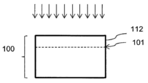
이를 위해, 도 3a를 참조하여, 제1 실시 예에 따라, 2원 조성 ABO3의 재료의 도너 기판(100)이 제공되고, 씨드층을 형성하도록 의도된, 전사되어야 할 단결정 층(102)을 한정하는 취성 영역(101)이 이온 주입(화살표들에 의해 도식적으로 도시됨)에 의해 형성된다. 이 도면에서, 도너 기판(100)은 동종적인(homogeneous) 것으로 나타내지만, 전술한 바와 같이, 대안적으로 복합 재료일 수 있다. 유리하게도, 논의되고 있는 상기 압전 재료에 따라, 상기 주입된 종들은 수소 및/또는 헬륨이다. 통상의 기술자는 결정된 깊이에 상기 취성 영역을 형성하기 위해 이들 종들의 도즈(dose) 및 주입 에너지를 결정할 수 있을 것이며, 이것은 통상적으로 2㎛ 미만이며, 전형적으로 논의되고 있는 상기 재료 및 상기 주입된 종들에 따라 상기 도즈는 2E+16 내지 2E+17 이온 종들/㎠의 범위이며, 상기 주입 에너지는 30 keV 내지 500 keV이다. 매몰된 상기 취성 층은 통상의 기술자에게 알려진 임의의 다른 수단들, 예를 들어 상기 재료의 다공성화 또는 대안적으로 레이저 조사에 의해 얻어질 수 있다.3A, according to a first embodiment, a
도 3b를 참조하면, 본 방식으로 취성화된 도너 기판(100)이 리시버 기판(110) 상으로 결합되며, 여기서 상기 주입이 통과하여 달성된 상기 도너 기판의 표면이 결합 계면에 있다. 결합 전에 상기 도너 기판 및/또는 상기 리시버 기판은, 상기 전사 후에 상기 리시버 기판과 상기 씨드층 사이에 삽입될 수 전기적 절연층 또는 전기적 도전층(도시 안됨)에 의해 피복될 수도 있다.Referring to FIG. 3B, a
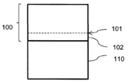
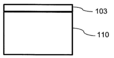
도 3c를 참조하면, 도너 기판(100)은 취성 영역(101)을 따라 분리된다. 그러한 분리는 당업자에게 공지된 임의의 수단, 예를 들어 열적, 기계적 또는 화학적 수단 등에 의해 달성될 수 있다. 도너 기판의 나머지는 회수되고, 재활용될 수 있으며, 층(102)이 리시버 기판(110) 상으로 전사될 수 있게 한다.Referring to FIG. 3C, the
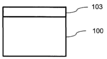
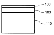
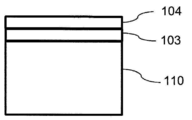
도 3d를 참조하면, 전사된 층(102)의 표면 부분은 예를 들어, 기계적 연마 및/또는 화학적 에칭에 의해 선택적으로 제거될 수 있다. 이러한 재료의 제거 목적은 상기 취성 영역 근처에서의 주입 및 분리와 관련된 임의의 결함들을 제거하기 위한 것이다. 이 제거 후에, 박막화된(thinned) 층(102)이 리시버 기판(110) 상에 얻어지며, 이는 다음의 에피택시 단계를 위한 씨드층으로서 작용할 것이다. 선택적으로, 도 3c의 전사된 층(102)은 에피택시를 위한 씨드층으로서 직접 사용될 수 있다.Referring to FIG. 3D, the surface portion of the transferred
도 3e를 참조하면, 조성 A'B'O3의 단결정 층(103)은 에피택셜 층(104)의 물질이 씨드층(102)의 물질과 상이한, 씨드층(102) 상에 에피택시에 의해 성장하도록 만들어진다. 따라서 씨드층(102)은 그것의 격자상수를 이용하며, 고품질의 단결정 재료가 성장할 수 있게 한다. 성장은 단결정 층에 요구되는 두께에 도달하면 중단된다. 최종 층(10)은 씨드층(102) 및 에피택셜층(103)의 스택으로부터 형성된다. 에피택셜층(103)의 조성은 점진적으로 또는 불연속적으로 그 내부의 상이한 깊이에서 변할 수 있다.3E, the
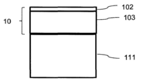
도 3e에서 보여지는 바와 같이, 직전에 기술된 방법 이후에, 표면 음향파 장치 또는 벌크 음향파 장치를 위한 기판이 얻어지며, 이것은 상기 리시버 기판(110) 및 상기 리시버 기판(110) 상의 단결정층(10)을 포함한다.3E, a substrate for a surface acoustic wave device or a bulk acoustic wave device is obtained, which is a single crystal layer (not shown) on the
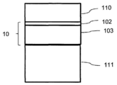
층(10)은:The layer (10) comprises:
- 상기 씨드층에 대응하는, 리시버 기판(110)과의 계면에 있는 제1 부분(102), A
- 상기 에피택셜 층에 대응하며, 조성 A'B'O3의 물질로 이루어지며, 여기서 상기 물질은 적어도 3원(ternary)이며, 상기 제1 부분(102)으로부터 연장되는 제2 부분(103)을 포함한다.- a second portion (103) extending from said first portion (102), said material corresponding to said epitaxial layer and consisting of a material of composition A'B'O 3 , said material being at least ternary, .
이 기판은 도 1에 도시된 바와 같은 표면 음향파 장치 또는 도 2에 도시된 바와 같은 벌크 음향파 장치, 또는 대안적으로 마이크로일렉트로닉스, 포토닉스 또는 집적 광학을 위한 다른 장치들을 제조하는데 유리하게 사용된다.This substrate is advantageously used to fabricate a surface acoustic wave device as shown in Fig. 1 or a bulk acoustic wave device as shown in Fig. 2, or alternatively other devices for microelectronics, photonics or integrated optics.
상기 씨드층은 전형적으로 2㎛ 미만, 바람직하게는 1㎛ 미만의 두께이다.The seed layer is typically less than 2 mu m thick, preferably less than 1 mu m thick.
에피택셜 층의 두께는 단결정층을 통합하려고 의도된 상기 장치의 사양들에 달려있다. 이와 관련하여, 상기 에피택셜 층의 두께는 최소값 또는 최대값의 관점들에서의 어느 하나로 제한되지 않는다. 순전히 정보를 위해, 아래 표는 상기 씨드층과 에피택셜층의 두께들의 조합들을 제공한다.The thickness of the epitaxial layer depends on the specifications of the device intended to incorporate the monocrystalline layer. In this regard, the thickness of the epitaxial layer is not limited to any of the minimum or maximum values. For purely information, the table below provides combinations of the thicknesses of the seed layer and the epitaxial layer.
도 4a 내지도 4e는 제2 실시 예에 따른 방법의 주요 단계들을 도시하며, 여기서 에피택시는 전사 전에 구현된다.도 4a를 참조하면, 조성 A'B'O3의 압전 재료를 포함하는 도너 기판(100)이 제공된다. 상기 도너 기판은 동종(도 4a에 도시된 바와 같이) 또는 복합체 일 수 있고; 후자의 경우 조성 A'B'O3의 표면층을 포함한다. 이것은 이러한 재료로 구성된 잉곳이 없다면, 상기 재료가 적어도 3원 이상인 경우가 특히 그러하다. 이어서, 에피택시에 의해 상기 재료 A'B'O3 상에 조성 A''B''O3의 단결정층(103)이 성장되도록 만들어지며, 상기 조성 A'B'O3의 물질은 상기 에피택시를 위한 씨드로서 사용된다. 에피택셜 층(103)의 물질은 도너 기판(100)의 물질과 동일하거나 상이할 수 있다.4A-4E show the main steps of the method according to the second embodiment, wherein the epitaxy is implemented prior to transfer. Referring to FIG. 4A, a donor substrate comprising a piezoelectric material of composition A'B'O 3 (100) is provided. The donor substrate may be homogeneous (as shown in FIG. 4A) or a complex; In the latter case, it includes the surface layer of the composition A'B'O 3 . This is especially true if the material is at least three or more, provided there is no ingot of such a material. Subsequently, a
그 다음, 취성 영역이 도너 기판(100)의 취성 영역 또는 조성 A''B''O3의 에피택셜층(103)에 형성되어, 전사될 층을 한정한다. 상기 취성 영역은 이온 종들의 주입에 의해 형성될 수 있다(도 4b의 화살표에 의해 도식적으로 도시됨).A brittle region is then formed in the brittle region of the
도 4b에 도시된 예에서, 취성 영역(101)은 에피택셜층(103) 아래의 도너 기판(100)에 형성된다. 이 경우, 전사될 층은 에피택셜층(103)의 전체 및 도너 기판(100)의 일부로 구성된다.In the example shown in FIG. 4B, the
다른 실시 예(도시되지 않음)에 따르면, 취성 영역은 층(103)에 형성된다. 이 경우에 전달될 층은 상기 층(103)의 자유 표면과 취성 영역(101) 사이에서 연장되는 부분으로 이루어진다.According to another embodiment (not shown), a brittle region is formed in
도 4c를 참조하면, 도너 기판은 리시버 기판(110) 상으로 결합되고, 조성 A''B''O3의 에피택셜층(103)이 결합 계면에 존재한다.Referring to FIG. 4C, the donor substrate is bonded onto the
도 4d를 참조하면, 도너 기판(100)은 도너 기판의 나머지 부분을 회수하고, 스택(103, 100')으로 구성된 상기 층을 리시버 기판(110) 상으로 전사하기 위해 취성 영역(101)을 따라 분리된다.4D, a
도 4e를 참조하면, 전사된 층의 적어도 표면 부분이 제거된다. 이 제거의 목적은 조성 A''B''O3의 물질을 노출시키도록 적어도 부분(100') 및 가능하게는 층 (103)의 일부를 제거하는 것이다.Referring to Figure 4E, at least the surface portion of the transferred layer is removed. The purpose of this removal is to remove at least part 100 'and possibly part of
이러한 방식으로 얻어진 층(103)은 표면 음향파 또는 벌크 음향파 장치를 제조하는데 사용될 수 있다.The
상기 제2 실시 예의 변형에 따라, 조성 A'''B'''O3의 부가적인 단결정층(104)을 형성하도록 조성 A''B''O3의 층(103) 상에 구현된 에피택시의 재개로 이루어진 도 4f에 도시된 추가의 단계가 수행된다. 상기 추가 층(104)의 물질은 층(103)의 물질과 동일할 수 있으며, 이 경우 에피택시의 후자의 단계는 층(103)의 후막화(thickening)를 야기한다(층(104)은 단지 가시적일 수 있도록 층(103)으로부터 분리되도록 도식적으로 표현되어 있지만, 최종 층에서는 가능하게도 그것의 품질을 제외하고는 분리되지는 않는다). 대안적으로, 추가 층(104)은 층(103)의 것과 상이한 재료로 제조된다.Wherein in accordance with a modification of the second embodiment, the composition A '''B''' O 3 of the additional epitaxial layer implemented on a single-
층(103) 및 가능하다면 층(104)의 두께는 상기 층을 통합시키려고 의도된 고주파수 장치의 사양에 따라 선택된다. 층(103)의 두께는 전형적으로 0.05 내지 2㎛이다. 층(104)의 두께는 전형적으로 0.5 내지 20 ㎛이다.The thickness of the
어떠한 구현이든, Smart CutTM 방법에 대한 대안(도시되지 않음)으로서, 도너 기판 및 리시버 기판의 결합 후에, 상기 씨드층이 노출될 때까지 상기 도너 기판의 예를 들어, 기계적 연마 및/또는 화학적 식각에 의한 물질의 제거를 통해 전사가 수행될 수 있다. 이 변형은 도너 기판의 소비를 수반하기 때문에 덜 유리하지만, Smart CutTM 방법은 도너 기판의 재활용을 가능하도록 허용한다. 반대로, 이 변형은 도너 기판 내에 주입을 필요로하지 않는다.Any implementation, as an alternative to the Smart Cut TM method (not shown), may be used after the combination of the donor and receiver substrates, for example by mechanical polishing and / or chemical etching of the donor substrate until the seed layer is exposed Lt; / RTI > can be carried out through the removal of the material by means of < RTI ID = 0.0 > This modification is less advantageous because it involves the consumption of donor substrates, but the Smart Cut TM method allows for the recycling of the donor substrate. Conversely, this modification does not require injection into the donor substrate.
도 4e 및 도 4f에서 볼 수 있는 바와 같이, 제2 실시 예에 따른 방법 후에, 표면 음향파 장치 또는 벌크 음향파 장치용 기판이 얻어지며, 이것은 리시버 기판(110) 및 상기 리시버 기판(110) 상의 조성 A''B''O3의 단결정층(103)을 포함하며, 그리고 적용 가능한 경우, 층(103) 상에 조성 A'''B'''O3의 층(104)을 포함한다.4E and 4F, after the method according to the second embodiment, a substrate for a surface acoustic wave device or a bulk acoustic wave device is obtained, which is formed on the
이 기판은 도 1에 도시된 바와 같은 표면 음향파 장치 또는 도 2에 도시된 바와 같은 벌크 음향파 장치를 제조하는데 유리하게 사용되며, 여기서 층(103) 또는 적용 가능하다면 층들(103 및 104) 모두는 도 1 및 도 2의 층(10)에 대응하거나, 또는 대안적으로 층을 포함하는 모든 다른 마이크로일렉스토닉스, 포토닉스 또는 광학 장치들에 대응한다.This substrate is advantageously used to manufacture a surface acoustic wave device as shown in Fig. 1 or a bulk acoustic wave device as shown in Fig. 2, where the
어떤 경우에는, 에피택셜 성장이 일어나는 상기 리시버 기판이 최종 용도에 최적이 아닐 수도 있다. 리시버 기판이 에피택시의 동작 조건을 거칠 것이기 때문에, 실제로는 적절한 재료들의 선택이 제한적이다. 특히, 리시버 기판은 에피택시 온도에 의해 손상될 수 있는 층들 또는 원소들을 포함할 수 없다. 그리고, 에피택셜층(103)(도 5a 참조)(또는 적용 가능하다면,104)의 표면을 통해 상기 기판(111) 상에 그것을 결합(bonding)함으로써 그리고 상기 리시버 기판(도 5b 참조)을 제거함으로써, 추구되는 용도에 따라 그 특성들이 선택되는 최종 기판(111) 상에 층(10)을 전사하는 것이 유리할 수 있다. 이 전사는 위에서 설명한 임의의 전사 기술로 수행할 수 있다. 최종 기판 상으로의 이러한 전사의 다른 이점은 에피택시로부터 생성된 구조에 매립된 씨드층(102)이 이어서 노출되고, 필요하다면, 특히 그것이 결함들을 가진다면 제거될 수 있다는 것이다(도 5c 참조). 원하는 특성을 갖는 에피택셜층(103)(그리고, 적용 가능한 경우, 층(104))(또는 상기 층의 일부)만이 최종 기판(111) 상에 남는다.In some cases, the receiver substrate where epitaxial growth occurs may not be optimal for end use. Since the receiver substrate will undergo the operating conditions of epitaxy, the choice of suitable materials is actually limited. In particular, the receiver substrate can not contain layers or elements that can be damaged by the epitaxy temperature. Then, by bonding it on the
표면 음향파 장치를 제조하기를 원한다면, 2개의 서로 맞물린 빗살 형태의 금속 전극들(12, 13)이 리시버 기판(110), 또는 적용 가능하다면 최종 기판 반대의 층(10)의 표면에 퇴적된다(이것이 리시버 기판(110)인지 또는 최종 기판(111)인지 막론하고, 상기 기판은 도 1에 도시된 지지 기판을 형성한다).Two interdigitated comb-shaped
벌크 음향파 장치를 제조하기를 원한다면, 상기 기술된 방법은 그에 따라 적합하게 되어야 한다. 먼저, 도 3b에 도시된 결합 단계 이전에, 도너 기판으로부터 전사될 층(102)의 자유 표면 상에 제1 전극이 퇴적되고, 이 제1 전극(도 2에서 참조 부호 13으로 지칭됨)은 최종 스택에 매몰된다. 도 3e에 도시된 에피택셜 성장 단계 후에, 제2 전극(도 2에서 12로 지칭됨)은 제1 전극에 대향하는 층(10)의 자유 표면 상에 퇴적된다. 또 다른 옵션은 전술한 바와 같이 최종 기판에 층을 전사하고, 상기 전사 전후에 상기 전극들을 형성하는 것이다. 둘째로, 리시버 기판(110) 내에서 전파하는 음향파를 방지하기 위해, 분리 수단이 상기 기판에 결합될 수 있으며, 이것은 예를 들어, 브래그 미러(도 2에 도시된 바와 같이) 또는 기판(110) 또는 적용 가능하다면 최종 기판(111)에 사전에 식각된 캐비티(cavity)일 수 있다.If it is desired to produce a bulk acoustic wave device, the method described above should be adapted accordingly. 3B, a first electrode is deposited on the free surface of the
어떤 구현이 선택되든지, 본 발명에 따른 방법은 2원성 뿐만아니라 3원성 또는 4원성인 단결정 층이 형성되도록 해주며, 따라서 표면 음향파 또는 벌크 음향파 장치들에 전통적으로 사용된 물질들보다 더 큰 상기 층에 대한 특성들의 선택을 허용하게 해준다. 이 수단들에 의해, 압전 재료의 결합 계수와 전기기계적 효율 사이의 만족할만한 절충이 보다 용이하게 얻어질 수 있다.Whichever implementation is chosen, the method according to the invention allows not only binary, but also ternary or quaternary monocrystalline layers to be formed, and thus greater than materials conventionally used in surface acoustic waves or bulk acoustic wave devices Allowing selection of properties for the layer. With these means, a satisfactory trade-off between the coupling coefficient of the piezoelectric material and the electromechanical efficiency can be obtained more easily.
이러한 압전 물질 해결책들의 발달이 특히 고려되는 다른 응용 분야는 마이크로-센서들 및 마이크로-액츄에이터들의 분야이다. 마이크로-센서들의 경우 목표는 일반적으로 외부의 응력에 의해 생성되는 변형을 측정하는 것일 것이다. 반면에, 마이크로-액츄에이터들의 경우, 목표는 연속적이거나 또는 가변적인 전기장의 인가를 통해 성분의 변형 또는 이동 부분의 변위를 야기하는 것을 추구할 것이다. 압전 물질의 사용은 기계적 변형 및 전기 신호와 관련될 수 있다. 예를 들어, 음향학 분야에서, 외부의 응력은 멤브레인을 변형시키는 압력파이다. 이는 가청 스펙트럼(audible spectrum) 내일 수 있고, 일반적으로 고려되는 대상들은 마이크로폰(센서 모드에서) 및 확성기들(액츄에이터 모드에서)이다. 이것은 예를 들어, 압전 미세기계 초음파 트랜듀서(Piezo Micromachined Ultrasonic Transducers, PMUT)의 제조를 위하여 가청 주파수들을 넘어 진행될 수 있다. 이는 또한 정적 압력 센서들, 또는 대안적으로 관성 센서들(가속 센서들, 자이로스코프들 등)과 관련될 수 있으며, 이를 위해 가속의 영향 하에서 이동되는 이동하는 질량의 운동이 압전 물질에 의해 측정된다. 압전 물질은 전체 변형된 성분(멤브레인, 빔, 칸티레버 등) 또는 유리하게는 변형 가능한 부분의 기계적 특성들을 더욱 개선하기 위하여 예를 들어, 실리콘과 같은 다른 물질들과 이것을 적층함으로써, 단지 이들의 일부분을 포함한다. 액츄에이터들의 카테고리에서, 압전 물질들은 매우 정밀한 변위를 조절할 수 있으며, 예를 들어 프린트 카트리지들로부터, 또는 마이크로-유체 시스템들로부터 잉크를 배출하기 위하여, 또는 대안적으로 광학 마이크로시스템의 초점 거리를 조정하기 위하여 사용될 수 있다.Other applications in which the development of these piezoelectric material solutions are particularly considered are in the field of micro-sensors and micro-actuators. In the case of micro-sensors, the goal would be to measure deformation usually produced by external stresses. On the other hand, in the case of micro-actuators, a target will seek to cause a deformation of the component or a displacement of the moving part through the application of a continuous or variable electric field. The use of piezoelectric materials may be related to mechanical deformation and electrical signals. For example, in the acoustics field, the external stress is the pressure wave that deforms the membrane. This can be within the audible spectrum and the objects generally considered are microphone (in sensor mode) and loudspeakers (in actuator mode). This can be done, for example, over audible frequencies for the fabrication of Piezo Micromachined Ultrasonic Transducers (PMUT). This may also be associated with static pressure sensors, or alternatively inertial sensors (such as acceleration sensors, gyroscopes, etc.), in which motion of a moving mass moving under the influence of acceleration is measured by a piezoelectric material . Piezoelectric materials can be formed by laminating them with other materials such as, for example, silicon, to further improve the mechanical properties of the entire deformed component (membrane, beam, cantilever, etc.) . In the category of actuators, the piezoelectric materials can control very precise displacements, for example to eject ink from print cartridges or from micro-fluid systems, or alternatively to adjust the focal distance of the optical microsystem Can be used.
참고문헌references
[1]
W. Steichen and S. Ballandras, "Acoustic components used for filtering - Review of the different technologies", Techniques de l'Ing ![]()
![]()
[2] Doctoral thesis (Dipl. Phys. ETH Zurich), "K1- yNayTa1 - xNbO3 thin film Electro-optics" (Diss. ETH No. 17275)[2] Doctoral thesis (.. Dipl Phys ETH Zurich), "K 1- y Na y Ta 1 - x NbO 3 thin film Electro-optics" (Diss ETH No. 17275.)
[3] L. S. Hung, J. A. Agostinelli, J. M. Mir, and L. R. Zheng, "Epitaxial nonlinear optical films of LiTaO3 grown on GaAs in waveguide form", Appl. Phys. Lett. 62 (24), 14 June 1993, p 3071[3] L. S. Hung, J. A. Agostinelli, J. M. Mir, and L. R. Zheng, "Epitaxial nonlinear optical films of LiTaO3 grown on GaAs in waveguide form", Appl. Phys. Lett. 62 (24), 14 June 1993, p. 3071
[4] E. Dogheche and D. Remiens, S. Shikata, A. Hachigo, and H. Nakahata , "High-frequency surface acoustic wave devices based on LiNbO3/diamond multilayered structure", APPLIED PHYSICS LETTERS 87, 213503, 2005[4] E. Dogheche and D. Remiens, S. Shikata, A. Hachigo, and H. Nakahata, "High-frequency surface acoustic wave devices based on LiNbO3 / diamond multilayered structure", APPLIED PHYSICS LETTERS 87, 213503, 2005
[5]
A. Bartasyte, V. Plausinaitiene, A. Abrutis, T. Murauskas, P. Boulet, S. Margueron, J. Gleize, S. Robert, V.Kubilius, and Z. Saltyte, "Residual stresses and clamped thermal expansion in LiNbO3 and LiTaO3 thin films", APPLIED PHYSICS LETTERS 101, 122902 (2012)[5]
A. Bartasyte, V. Plausinaitiene, A. Abrutis, T. Murauskas, P. Boulet, S. Margueron, J. Gleize, S. Robert, V. Kubilius, and Z. Saltyte, "Residual stresses and clamped thermal expansion in LiNbO3 and LiTaO3 thin films ",
[6] Letters to Nature, Nature 432, 84-87 (4 November 2004) doi: 10.1038/nature03028; "Lead-free piezoceramics", Yasuyoshi Saito, Hisaaki Takao, Toshihiko Tani, Tatsuhiko Nonoyama, Kazumasa Takatori, Takahiko Homma, Toshiatsu Nagaya & Masaya Nakamura[6] Letters to Nature, Nature 432, 84-87 (4 November 2004) doi: 10.1038 / nature03028; "Lead-free piezoceramics", Yasuyoshi Saito, Hisaaki Takao, Toshihiko Tani, Tatsuhiko Nonoyama, Kazumasa Takatori, Takahiko Homma, Toshiatsu Nagaya & Masaya Nakamura
Claims (29)
- 조성 ABO3의 압전 물질을 포함하는 도너 기판(100)을 제공하는 단계로서, 여기서 A는 Li, Na, K, H 중의 적어도 하나의 원소로 구성되며, B는 Nb, Ta, Sb, V 중의 적어도 하나의 원소로 구성되는, 상기 제공하는 단계;
- 리시버 기판(110)을 공급하는 단계;
- 상기 리시버 기판 상에 상기 도너 기판을 결합시킴으로써 상기 리시버 기판(110) 상으로 상기 도너 기판(100)으로부터 "씨드층"이라 지칭되는 층(102)을 전사하는 단계로서, 상기 씨드층(102)은 결합 계면에 있게 하며, 상기 씨드층(102)까지 상기 도너 기판(100)의 박막화(thinning)가 이어지는, 상기 전사하는 단계;
- 상기 씨드층(102)의 압전 물질 ABO3 상에 에피택시에 의해 조성 A'B'O3의 단결정층(103)을 성장시키는 단계로서, 여기서 A'는 다음 원소들 Li, Na, K, H 중의 적어도 하나로 구성되며, B'는 다음 원소들 Nb, Ta, Sb, V 중의 적어도 하나로 구성되며, A'는 A와 상이하거나 또는 B'는 B와 상이한, 상기 성장시키는 단계;
를 연속적으로 포함하는 것을 특징으로 하는 단결정 층의 제조 방법.As a method for producing the single crystal layer 10,
Providing a donor substrate 100 comprising a piezoelectric material of composition ABO 3 wherein A comprises at least one element of Li, Na, K, H and B is at least one element selected from the group consisting of Nb, Ta, Sb, V The method comprising: providing at least one element;
- feeding the receiver substrate (110);
- transferring a layer (102) referred to as a " seed layer " from the donor substrate (100) onto the receiver substrate (110) by engaging the donor substrate on the receiver substrate, Wherein the donor substrate 100 is at a bonding interface and the donor substrate 100 is thinned to the seed layer 102;
- growing a monocrystalline layer (103) of composition A'B'O 3 by epitaxy on the piezoelectric material ABO 3 of the seed layer (102), wherein A 'is at least one element selected from the group consisting of Li, Na, K, H, B 'is composed of at least one of the following elements Nb, Ta, Sb, V, wherein A' is different from A or B 'is different from B;
Wherein the single crystal layer comprises a single crystal.
A'는 A와 마찬가지로 적어도 하나의 원소를 포함하며, 및/또는 B'는 B와 마찬가지로 적어도 하나의 원소를 포함하는 것을 특징으로 하는 단결정 층의 제조방법.The method according to claim 1,
A 'comprises at least one element as in A, and / or B' comprises at least one element as in B.
B'가 B와 상이할 경우 A'는 A와 동일하며, 그리고 A'가 A와 상이할 경우 B'는 B와 동일한 것을 특징으로 하는 단결정 층의 제조방법.The method according to claim 1,
A 'is the same as A when B' is different from B, and B 'is equal to B when A' is different from A.
A는 단일 원소로 구성되며, 그리고 B도 단일 원소로 구성되는 것을 특징으로 하는 단결정 층의 제조방법.The method according to any one of claims 1 to 3,
Wherein A is composed of a single element, and B is composed of a single element.
상기 씨드층(102)을 전사하는 단계는,
- 상기 조성 ABO3의 압전 물질을 포함하며, 상기 씨드층이라 지칭되는 층을 제한하도록 상기 도너 기판(100)에 취성 영역(101)을 형성하는 단계;
- 상기 씨드층(102)이 결합 계면에 있도록, 상기 리시버 기판(110) 상에 상기 도너 기판(100)을 결합시키는 단계;
- 상기 씨드층(102)을 상기 리시버 기판(110) 상으로 전사하기 위해 상기 취성 영역(101)을 따라 상기 도너 기판(100)을 분리하는 단계;
를 포함하는 것을 특징으로 하는 단결정 층의 제조방법.The method according to any one of claims 1 to 4,
The step of transferring the seed layer (102)
- forming a brittle zone (101) in the donor substrate (100) to limit the layer referred to as the seed layer, comprising the piezoelectric material of the composition ABO 3 ;
- coupling the donor substrate (100) onto the receiver substrate (110) so that the seed layer (102) is at the bonding interface;
- separating the donor substrate (100) along the embrittlement region (101) to transfer the seed layer (102) onto the receiver substrate (110);
And forming a single crystal layer on the substrate.
상기 에피택시의 단계 전에, 상기 리시버 기판(110) 상으로 전사된 상기 씨드층(102)의 두께의 일부가 제거되는 것을 특징으로 하는 단결정 층의 제조방법.The method of claim 5,
Wherein a portion of the thickness of the seed layer (102) transferred onto the receiver substrate (110) is removed prior to the step of epitaxy.
상기 씨드층(102)의 두께는 2 ㎛ 미만이며, 바람직하게는 1 ㎛ 미만인 것을 특징으로 하는 단결정 층의 제조 방법.The method according to any one of claims 1 to 6,
Wherein the thickness of the seed layer (102) is less than 2 占 퐉, preferably less than 1 占 퐉.
상기 리시버 기판은 반도체 물질로 이루어지며, 그리고 상기 씨드층과 상기 리시버 기판 사이에 중간 전하-트랩핑 층을 포함하는 것을 특징으로 하는 단결정 층의 제조방법.The method according to any one of claims 1 to 7,
Wherein the receiver substrate comprises a semiconductor material and an intermediate charge-trapping layer between the seed layer and the receiver substrate.
- 조성 A'B'O3의 압전 물질을 포함하는 도너 기판(100)을 제공하는 단계로서, 여기서 A'는 다음 원소들 Li, Na, K, H 중의 적어도 하나 이상으로 구성되며, B'는 다음 원소들 Nb, Ta, Sb, V 중의 적어도 하나 이상으로 구성되는, 상기 제공하는 단계;
- 상기 압전 물질 A'B'O3 상에 에피택시에 의해 조성 A''B''O3의 단결정층(103)을 성장시키는 단계로서, 여기서 A''는 다음 원소들 Li, Na, K, H 중의 하나 이상으로 구성되며, B''는 다음 원소들 Nb, Ta, Sb, V 중의 하나 이상으로 구성되는, 상기 성장시키는 단계;
- 리시버 기판(110)을 공급하는 단계;
- 에피택셜 층(103)을 통하여 상기 리시버 기판(110) 상에 상기 도너 기판(100)을 결합시킴으로써 상기 리시버 기판(110) 상으로 조성 A''B''O3의 상기 에피택셜 층(103)의 적어도 일부를 전사하는 단계로서, 조성 A''B''O3의 상기 에피택셜 층(103)까지 상기 도너 기판(100)의 박막화가 이어지는, 상기 전사하는 단계;
를 연속적으로 포함하는 것을 특징으로 하는 단결정 층의 제조 방법.As a method for producing the single crystal layer 10,
- providing a donor substrate (100) comprising a piezoelectric material of composition A'B'O 3 , wherein A 'consists of at least one of the following elements Li, Na, K, H, and B' Comprising at least one of the following elements Nb, Ta, Sb, V;
- growing a single crystal layer (103) of composition A "B" O 3 by epitaxy on said piezoelectric material A'B'O 3 , wherein A "comprises the following elements Li, Na, K , H, and B "comprises at least one of the following elements Nb, Ta, Sb, V;
- feeding the receiver substrate (110);
- epitaxial layer 103 of composition A '' B '' O 3 onto the receiver substrate 110 by coupling the donor substrate 100 onto the receiver substrate 110 through the epitaxial layer 103. ) of the method comprising: transferring at least a portion, the method comprising the transfer is thinning of the donor substrate 100, leading up to the epitaxial layer 103 of composition A''B''O 3;
Wherein the single crystal layer comprises a single crystal.
조성 A''B''O3의 층(103)이 상기 리시버 기판 상으로 전사된 후에, 상기 조성 A''B''O3의 물질 상에, 에피택시에 의해 조성 A'''B'''O3의 단결정 층(104)을 성장시키는 단계를 포함하며, 여기서 A'''는 다음 원소들 Li, Na, K, H 중의 하나 이상으로 구성되며, B'''는 다음 원소들 Nb, Ta, Sb, V 중의 하나 이상으로 구성되는, 것을 특징으로 하는 단결정 층의 제조방법.The method of claim 9,
After layer 103 of composition A''B''O 3 is transferred onto the receiver substrate, and on a material of the composition A''B''O 3, by epitaxy composition A '''B''', and a step of growing a single-crystal layer 104 of the O 3, wherein a '''is composed of one or more of the following elements of Li, Na, K, H, B''' has the following elements Nb , Ta, Sb, and V. The method of manufacturing a single crystal layer according to claim 1,
A'''는 A''와 상이하거나 또는 B'''는 B''와 상이한 것을 특징으로 하는 단결정 층의 제조방법.The method of claim 10,
A '''is different from A''orB''' is different from B ''.
상기 리시버 기판(110) 상으로 조성 A''B''O3의 상기 에피택셜층(103)의 적어도 일부를 전사하는 단계는,
- 전사되어지는 층을 제한하기 위해, 상기 도너 기판(100) 내에 또는 조성 A''B''O3의 상기 에피택셜층(103) 내에 취성 영역(101)을 형성하는 단계;
- 조성 A''B''O3의 상기 에피택셜층(103)이 결합 계면에 있도록, 상기 리시버 기판(110) 상에 상기 도너 기판(100)을 결합시키는 단계;
- 상기 취성 영역(101)을 따라 상기 도너 기판(100) 또는 상기 에피택셜층(103)을 분리하는 단계;
를 포함하는 것을 특징으로 하는 단결정 층의 제조방법.The method according to any one of claims 9 to 11,
The step of transferring at least a portion of the epitaxial layer 103 of the composition A " B " O 3 onto the receiver substrate 110 comprises:
- forming an embrittlement zone (101) in the donor substrate 3 or the composition of the epitaxial layer in the (100) A''B''O (103) for limiting the layer which is transferred;
Bonding the donor substrate 100 on the receiver substrate 110 such that the epitaxial layer 103 of the composition A''B "O 3 is at the bonding interface;
- separating the donor substrate (100) or the epitaxial layer (103) along the brittle region (101);
And forming a single crystal layer on the substrate.
상기 취성 영역(101)은 상기 도너 기판(100) 내에 형성되며, 상기 전사하는 단계 후에, 전사된 상기 층(100',100)은 조성 A''B''O3의 물질을 노출시키도록 박막화되는 것을 특징으로 하는 단결정 층의 제조방법.The method of claim 12,
The brittle region 101 is formed in the donor substrate 100 and after the transfer step the transferred layers 100 'and 100 are thinned to expose the material of composition A''B''O 3 Wherein the single-crystal layer is a single crystal layer.
A''는 A'와 상이하거나 또는 B''는 B'와 상이한 것을 특징으로 하는 단결정 층의 제조방법.The method according to any one of claims 9 to 13,
A " is different from A 'or B " is different from B'.
A''는 A'와 마찬가지로 적어도 하나의 원소를 포함하며, 및/또는 B''는 B'와 마찬가지로 적어도 하나의 원소를 포함하는 것을 특징으로 하는 단결정 층의 제조방법.The method according to any one of claims 9 to 13,
A "comprises at least one element as in A ', and / or B" comprises at least one element as well as B'.
B''가 B'와 상이할 경우 A''는 A'와 동일하며, 그리고 A''가 A'와 상이할 경우 B''는 B'와 동일한 것을 특징으로 하는 단결정 층의 제조방법.The method according to any one of claims 9 to 13,
Wherein A "is the same as A 'when B" is different from B', and B "is the same as B 'when A" is different from A'.
A'는 단일 원소로 구성되며, 그리고 B'도 단일 원소로 구성되는 것을 특징으로 하는 단결정 층의 제조방법.The method according to any one of claims 9 to 16,
A 'is composed of a single element, and B' is also a single element.
상기 취성 영역(101)은 상기 도너 기판(100) 내에 이온 주입에 의해 형성되는 것을 특징으로 하는 단결정 층의 제조방법.The method according to claim 5 or 12,
Wherein the brittle region (101) is formed in the donor substrate (100) by ion implantation.
에피택시 단계 후에, 조성 A''B''O3의 단결정 층(103)의 두께는 0.2 내지 20 ㎛ 인 것을 특징으로 하는 단결정 층의 제조방법.The method according to any one of claims 1 to 18,
After phase epitaxy, the thickness of the single-crystal layer 103 of the composition A''B''O 3 is method of producing a single-crystal layer, characterized in that 0.2 to 20 ㎛.
상기 리시버 기판과 상기 도너 기판 사이의 계면에 적어도 하나의 전기적 절연층 및/또는 적어도 하나의 전기적 도전층이 형성되는 것을 특징으로 하는 단결정 층의 제조방법.The method according to any one of claims 1 to 19,
Wherein at least one electrically insulating layer and / or at least one electrically conductive layer is formed on the interface between the receiver substrate and the donor substrate.
최종 기판(111) 상으로 상기 리시버 비판의 단결정 층(103,104)의 적어도 일부를 전사시키는 단계를 포함하는 것을 특징으로 하는 단결정 층의 제조방법.The method according to any one of claims 1 to 20,
And transferring at least a part of the single crystal layers (103, 104) of the receiver criterion onto the final substrate (111).
지지 기판(110),
상기 지지 기판 상에 조성 A''B''O3의 단결정 층(103)으로서, 여기서 A''는 다음 원소들 Li, Na, K, H 중의 하나 이상으로 구성되며, B''는 다음 원소들 Nb, Ta, Sb, V 중의 하나 이상으로 구성되며, A'' 및 B'' 중의 적어도 하나는 적어도 두개의 원소들로 구성되는, 상기 단결정 층(103),
그리고 상기 지지 기판(110)과 조성 A''B''O3의 상기 층(103) 사이에 조성 A'B'O3의 층(102)으로서, 여기서 A'는 다음 원소들 Li, Na, K, H 중의 적어도 하나의 원소로 구성되며, B'는 다음 원소들 Nb, Ta, Sb, V 중의 적어도 하나의 원소로 구성되는, 상기 층(102),을 포함하는 것을 특징으로 하는 기판.1. A substrate for a microelectronic, photonic or optical device,
The support substrate 110,
Wherein A "consists of one or more of the following elements Li, Na, K, H and B" is a single crystal layer of composition A "B" O 3 on the support substrate: And at least one of A " and B " is composed of at least two elements, the single crystal layer (103), the single crystal layer
And a layer 102 of a composition A'B'O 3 between the support substrate 110 and the layer 103 of the composition A''B''O3 where A 'is at least one of the following elements Li, Na, K , H, and B 'is composed of at least one of the following elements: Nb, Ta, Sb, V.
조성 A''B''O3의 상기 층(103) 상에, 조성 A'''B'''O3의 단결정 층(104)을 더 포함하며, 여기서 A'''는 다음 원소들 Li, Na, K, H 중의 하나 이상으로 구성되며, B'''는 다음 원소들 Nb, Ta, Sb, V 중의 하나 이상으로 구성되는 것을 특징으로 하는 기판.23. The method of claim 22,
The composition on the layer 103 of A''B''O 3, composition A 'further includes a single-crystal layer 104 of the 3' 'B''' O, where A '''has the following elements Li , Na, K, H, and B '''consists of at least one of the following elements Nb, Ta, Sb,
청구항 1 내지 청구항 21 중의 어느 하나의 청구항에 따른 제조방법에 의해 얻어질 수 있는 단결정 압전층(10), 및
상기 단결정 압전층의 표면에 형성된 두개의 전극들(12,13)을 포함하는 것을 특징으로 하는 표면 음향파 장치.As a surface acoustic wave device,
A single crystal piezoelectric layer (10) obtainable by a manufacturing method according to any one of claims 1 to 21, and
And two electrodes (12, 13) formed on the surface of the single crystal piezoelectric layer.
청구항 1 내지 청구항 21 중의 어느 하나의 청구항에 따른 제조방법에 의해 얻어질 수 있는 단결정 압전층(10), 및
상기 단결정 압전층의 두 개의 반대측 면들에 형성된 두 개의 전극들(12,13)을 포함하는 것을 특징으로 하는 벌크 음향파 장치.As a bulk acoustic wave device,
A single crystal piezoelectric layer (10) obtainable by a manufacturing method according to any one of claims 1 to 21, and
And two electrodes (12, 13) formed on two opposite sides of the single crystal piezoelectric layer.
Applications Claiming Priority (3)
| Application Number | Priority Date | Filing Date | Title |
|---|---|---|---|
| FR1563055A FR3045677B1 (en) | 2015-12-22 | 2015-12-22 | PROCESS FOR PRODUCING A MONOCRYSTALLINE LAYER, IN PARTICULAR PIEZOELECTRIC |
| FR1563055 | 2015-12-22 | ||
| PCT/EP2016/082245 WO2017108994A1 (en) | 2015-12-22 | 2016-12-21 | Method for the production of a single-crystal film, in particular piezoelectric |
Publications (2)
| Publication Number | Publication Date |
|---|---|
| KR20180098343A true KR20180098343A (en) | 2018-09-03 |
| KR102681655B1 KR102681655B1 (en) | 2024-07-05 |
Family
ID=55590008
Family Applications (1)
| Application Number | Title | Priority Date | Filing Date |
|---|---|---|---|
| KR1020187021267A Active KR102681655B1 (en) | 2015-12-22 | 2016-12-21 | Manufacturing method of single crystal layer, especially piezoelectric layer |
Country Status (8)
| Country | Link |
|---|---|
| US (3) | US11101428B2 (en) |
| EP (1) | EP3394324A1 (en) |
| JP (1) | JP6816147B2 (en) |
| KR (1) | KR102681655B1 (en) |
| CN (2) | CN108603305A (en) |
| FR (1) | FR3045677B1 (en) |
| SG (1) | SG11201805382SA (en) |
| WO (1) | WO2017108994A1 (en) |
Families Citing this family (13)
| Publication number | Priority date | Publication date | Assignee | Title |
|---|---|---|---|---|
| US20180048283A1 (en) * | 2015-04-16 | 2018-02-15 | Shin-Etsu Chemical Co., Ltd. | Lithium tantalate single crystal substrate, bonded substrate, manufacturing method of the bonded substrate, and surface acoustic wave device using the bonded substrate |
| FR3045677B1 (en) * | 2015-12-22 | 2019-07-19 | Soitec | PROCESS FOR PRODUCING A MONOCRYSTALLINE LAYER, IN PARTICULAR PIEZOELECTRIC |
| JP6654435B2 (en) * | 2016-01-07 | 2020-02-26 | 株式会社ディスコ | Wafer generation method |
| KR102063051B1 (en) * | 2016-11-25 | 2020-01-07 | 주식회사 엘지화학 | Curable Composition |
| FR3073083B1 (en) * | 2017-10-31 | 2019-10-11 | Soitec | METHOD FOR MANUFACTURING A FILM ON A FLEXIBLE SHEET |
| FR3108789B1 (en) * | 2020-03-24 | 2023-12-08 | Soitec Silicon On Insulator | Method for manufacturing a piezoelectric structure for a radio frequency device and which can be used for the transfer of a piezoelectric layer, and method for transferring such a piezoelectric layer |
| CN113926680B (en) * | 2021-09-01 | 2022-12-13 | 中国电子科技集团公司第三研究所 | Ultrasonic transducer, ultrasonic scanning microscope and manufacturing method of ultrasonic transducer |
| FR3131800B1 (en) * | 2022-01-07 | 2024-03-22 | Soitec Silicon On Insulator | Substrate treatment process |
| CN114774844A (en) * | 2022-03-31 | 2022-07-22 | 清华大学 | Method for regulating and controlling flat surface components of thin film at atomic level |
| CN115472734A (en) * | 2022-08-31 | 2022-12-13 | 中国电子科技集团公司第二十六研究所 | Perovskite type Relaxor-PT solid solution single crystal film composite material and preparation method thereof |
| FR3141308B1 (en) * | 2022-10-20 | 2024-10-11 | Soitec Silicon On Insulator | METHOD FOR PRODUCING A PIEZOELECTRIC LAYER ON A SUBSTRATE |
| EP4414482A1 (en) * | 2023-02-07 | 2024-08-14 | Max-Planck-Gesellschaft zur Förderung der Wissenschaften e.V. | Composite substrates for the epitaxial growth of thin films and method for fabricating such substrates |
| CN117156947B (en) * | 2023-10-31 | 2024-02-20 | 北京青禾晶元半导体科技有限责任公司 | A kind of preparation method of composite piezoelectric substrate |
Citations (3)
| Publication number | Priority date | Publication date | Assignee | Title |
|---|---|---|---|---|
| US6593212B1 (en) * | 2001-10-29 | 2003-07-15 | The United States Of America As Represented By The Secretary Of The Navy | Method for making electro-optical devices using a hydrogenion splitting technique |
| KR20120084295A (en) * | 2009-10-09 | 2012-07-27 | 꼼미사리아 아 레네르지 아토미끄 에뜨 옥스 에너지스 앨터네이티브즈 | Acoustic wave device including a surface wave filter and a bulk wave filter, and method for making same |
| KR20190061070A (en) * | 2016-10-10 | 2019-06-04 | 소이텍 | Surface-type image sensor and method of manufacturing the sensor |
Family Cites Families (35)
| Publication number | Priority date | Publication date | Assignee | Title |
|---|---|---|---|---|
| US2738939A (en) | 1954-07-13 | 1956-03-20 | Francis M Johnson | Personnel retriever for helicopters |
| US4019200A (en) | 1975-06-11 | 1977-04-19 | Rockwell International Corporation | Monolithic surface acoustic wave signal storage device |
| JPH08153915A (en) | 1994-11-30 | 1996-06-11 | Matsushita Electric Ind Co Ltd | Composite piezoelectric substrate and manufacturing method thereof |
| CN1048126C (en) | 1994-12-06 | 2000-01-05 | 株式会社村田制作所 | Electrode forming method for surface acoustic wave device |
| US5935641A (en) | 1996-10-23 | 1999-08-10 | Texas Instruments Incorporated | Method of forming a piezoelectric layer with improved texture |
| US6120597A (en) | 1998-02-17 | 2000-09-19 | The Trustees Of Columbia University In The City Of New York | Crystal ion-slicing of single-crystal films |
| US6540827B1 (en) * | 1998-02-17 | 2003-04-01 | Trustees Of Columbia University In The City Of New York | Slicing of single-crystal films using ion implantation |
| JP2001122699A (en) * | 1999-10-21 | 2001-05-08 | Murata Mfg Co Ltd | Oxide substrate for producing epitaxial film, method of producing epitaxial film and piezoelectric device |
| JP3704017B2 (en) | 2000-03-28 | 2005-10-05 | ヤマハ株式会社 | Surface acoustic wave device |
| US6555946B1 (en) | 2000-07-24 | 2003-04-29 | Motorola, Inc. | Acoustic wave device and process for forming the same |
| JP4055405B2 (en) | 2001-12-03 | 2008-03-05 | ソニー株式会社 | Electronic component and manufacturing method thereof |
| US6767749B2 (en) * | 2002-04-22 | 2004-07-27 | The United States Of America As Represented By The Secretary Of The Navy | Method for making piezoelectric resonator and surface acoustic wave device using hydrogen implant layer splitting |
| FR2845523B1 (en) | 2002-10-07 | 2005-10-28 | METHOD FOR MAKING A SUBSTRATE BY TRANSFERRING A DONOR WAFER HAVING FOREIGN SPECIES, AND ASSOCIATED DONOR WAFER | |
| FR2847076B1 (en) | 2002-11-07 | 2005-02-18 | Soitec Silicon On Insulator | METHOD OF DETACHING A THIN LAYER AT MODERATE TEMPERATURE AFTER CO-IMPLANTATION |
| JP3774782B2 (en) | 2003-05-14 | 2006-05-17 | 富士通メディアデバイス株式会社 | Manufacturing method of surface acoustic wave device |
| WO2005050836A1 (en) | 2003-11-19 | 2005-06-02 | Murata Manufacturing Co., Ltd. | End surface reflection surface acoustic wave device and its manufacturing method |
| US7863157B2 (en) | 2006-03-17 | 2011-01-04 | Silicon Genesis Corporation | Method and structure for fabricating solar cells using a layer transfer process |
| JP4091641B2 (en) | 2006-04-07 | 2008-05-28 | 富士フイルム株式会社 | Piezoelectric element, manufacturing method thereof, and ink jet recording head |
| JP2008211277A (en) | 2007-02-23 | 2008-09-11 | Matsushita Electric Ind Co Ltd | Surface acoustic wave device |
| US8239052B2 (en) * | 2007-04-13 | 2012-08-07 | National Institute Of Advanced Industrial Science And Technology | Sound source separation system, sound source separation method, and computer program for sound source separation |
| US7750406B2 (en) | 2007-04-20 | 2010-07-06 | International Business Machines Corporation | Design structure incorporating a hybrid substrate |
| US7982363B2 (en) | 2007-05-14 | 2011-07-19 | Cree, Inc. | Bulk acoustic device and method for fabricating |
| JP5181649B2 (en) * | 2007-09-18 | 2013-04-10 | 日立電線株式会社 | Piezoelectric element |
| CN101689841A (en) | 2007-12-25 | 2010-03-31 | 株式会社村田制作所 | Method for manufacturing composite piezoelectric substrate |
| US8115365B2 (en) * | 2008-04-15 | 2012-02-14 | Ngk Insulators, Ltd. | Surface acoustic wave devices |
| ATE555494T1 (en) | 2009-02-19 | 2012-05-15 | S O I Tec Silicon | RELAXATION AND TRANSFER OF STRESSED MATERIAL LAYERS |
| JP5429200B2 (en) | 2010-05-17 | 2014-02-26 | 株式会社村田製作所 | Method for manufacturing composite piezoelectric substrate and piezoelectric device |
| JP2012106902A (en) * | 2010-10-25 | 2012-06-07 | Fujifilm Corp | Perovskite-type oxide film, ferroelectric film using the same, ferroelectric device, and method for manufacturing perovskite-type oxide film |
| JP5811173B2 (en) * | 2011-03-22 | 2015-11-11 | 株式会社村田製作所 | Method for manufacturing piezoelectric device |
| CN102253451B (en) | 2011-05-13 | 2013-03-20 | 华中科技大学 | Preparation method of lithium niobate optical waveguide |
| EP2738939B1 (en) * | 2011-07-29 | 2018-12-05 | Murata Manufacturing Co., Ltd. | Piezoelectric device and method of manufacturing piezoelectric device |
| JPWO2014020906A1 (en) | 2012-07-30 | 2016-07-21 | 住友化学株式会社 | Manufacturing method of composite substrate and manufacturing method of semiconductor crystal layer forming substrate |
| FR2995136B1 (en) | 2012-09-04 | 2015-06-26 | Soitec Silicon On Insulator | PSEUDO-SUBSTRATE WITH IMPROVED EFFICIENCY OF USE OF MONOCRYSTALLINE MATERIAL |
| US9324931B2 (en) | 2013-05-14 | 2016-04-26 | Tdk Corporation | Piezoelectric device |
| FR3045677B1 (en) * | 2015-12-22 | 2019-07-19 | Soitec | PROCESS FOR PRODUCING A MONOCRYSTALLINE LAYER, IN PARTICULAR PIEZOELECTRIC |
-
2015
- 2015-12-22 FR FR1563055A patent/FR3045677B1/en active Active
-
2016
- 2016-12-21 SG SG11201805382SA patent/SG11201805382SA/en unknown
- 2016-12-21 JP JP2018532582A patent/JP6816147B2/en active Active
- 2016-12-21 CN CN201680080405.8A patent/CN108603305A/en active Pending
- 2016-12-21 EP EP16819558.4A patent/EP3394324A1/en active Pending
- 2016-12-21 CN CN202411652636.4A patent/CN119553364A/en active Pending
- 2016-12-21 US US16/064,416 patent/US11101428B2/en active Active
- 2016-12-21 KR KR1020187021267A patent/KR102681655B1/en active Active
- 2016-12-21 WO PCT/EP2016/082245 patent/WO2017108994A1/en not_active Ceased
-
2021
- 2021-08-06 US US17/396,374 patent/US12356858B2/en active Active
-
2025
- 2025-06-05 US US19/229,438 patent/US20250301910A1/en active Pending
Patent Citations (3)
| Publication number | Priority date | Publication date | Assignee | Title |
|---|---|---|---|---|
| US6593212B1 (en) * | 2001-10-29 | 2003-07-15 | The United States Of America As Represented By The Secretary Of The Navy | Method for making electro-optical devices using a hydrogenion splitting technique |
| KR20120084295A (en) * | 2009-10-09 | 2012-07-27 | 꼼미사리아 아 레네르지 아토미끄 에뜨 옥스 에너지스 앨터네이티브즈 | Acoustic wave device including a surface wave filter and a bulk wave filter, and method for making same |
| KR20190061070A (en) * | 2016-10-10 | 2019-06-04 | 소이텍 | Surface-type image sensor and method of manufacturing the sensor |
Also Published As
| Publication number | Publication date |
|---|---|
| JP2019508924A (en) | 2019-03-28 |
| SG11201805382SA (en) | 2018-07-30 |
| FR3045677A1 (en) | 2017-06-23 |
| US11101428B2 (en) | 2021-08-24 |
| US20250301910A1 (en) | 2025-09-25 |
| US20180375014A1 (en) | 2018-12-27 |
| CN119553364A (en) | 2025-03-04 |
| JP6816147B2 (en) | 2021-01-20 |
| KR102681655B1 (en) | 2024-07-05 |
| US20210367139A1 (en) | 2021-11-25 |
| FR3045677B1 (en) | 2019-07-19 |
| US12356858B2 (en) | 2025-07-08 |
| CN108603305A (en) | 2018-09-28 |
| WO2017108994A1 (en) | 2017-06-29 |
| EP3394324A1 (en) | 2018-10-31 |
Similar Documents
| Publication | Publication Date | Title |
|---|---|---|
| US12356858B2 (en) | Method for the production of a single-crystal film, in particular piezoelectric | |
| US20230217832A1 (en) | Composite substrates including epitaxial monocrystalline piezoelectric layers bonded to substrates, and acoustic wave devices formed with such composite substrates | |
| US11705880B2 (en) | Process for producing a micro-electro-mechanical system from a transferred piezoelectric or ferroelectric layer | |
| KR101806578B1 (en) | Acoustic wave device including a surface wave filter and a bulk wave filter, and method for making same | |
| US9496847B2 (en) | Electro-acoustic transducer with periodic ferroelectric polarization produced on a micromachined vertical structure | |
| KR102750357B1 (en) | Substrate for temperature-compensated surface acoustic wave devices or bulk acoustic wave devices | |
| JP2018506930A (en) | Plate wave device having wave confinement structure and fabrication method | |
| US20130130502A1 (en) | Micromechanical membranes and related structures and methods | |
| JP2014532360A (en) | Bulk wave resonators based on micromachined vertical structures | |
| Reinhardt et al. | Acoustic filters based on thin single crystal LiNbO 3 films: status and prospects | |
| CN205792476U (en) | A kind of FBAR using ultra-thin piezoelectric single crystal to make | |
| KR20230086718A (en) | Composite structure for MEMS applications including deformable layer and piezoelectric layer and related fabrication method | |
| KR102457258B1 (en) | How to make the layer |
Legal Events
| Date | Code | Title | Description |
|---|---|---|---|
| PA0105 | International application |
St.27 status event code: A-0-1-A10-A15-nap-PA0105 |
|
| P11-X000 | Amendment of application requested |
St.27 status event code: A-2-2-P10-P11-nap-X000 |
|
| P13-X000 | Application amended |
St.27 status event code: A-2-2-P10-P13-nap-X000 |
|
| PG1501 | Laying open of application |
St.27 status event code: A-1-1-Q10-Q12-nap-PG1501 |
|
| A201 | Request for examination | ||
| PA0201 | Request for examination |
St.27 status event code: A-1-2-D10-D11-exm-PA0201 |
|
| P22-X000 | Classification modified |
St.27 status event code: A-2-2-P10-P22-nap-X000 |
|
| P22-X000 | Classification modified |
St.27 status event code: A-2-2-P10-P22-nap-X000 |
|
| E902 | Notification of reason for refusal | ||
| PE0902 | Notice of grounds for rejection |
St.27 status event code: A-1-2-D10-D21-exm-PE0902 |
|
| T11-X000 | Administrative time limit extension requested |
St.27 status event code: U-3-3-T10-T11-oth-X000 |
|
| E13-X000 | Pre-grant limitation requested |
St.27 status event code: A-2-3-E10-E13-lim-X000 |
|
| P11-X000 | Amendment of application requested |
St.27 status event code: A-2-2-P10-P11-nap-X000 |
|
| P13-X000 | Application amended |
St.27 status event code: A-2-2-P10-P13-nap-X000 |
|
| E701 | Decision to grant or registration of patent right | ||
| PE0701 | Decision of registration |
St.27 status event code: A-1-2-D10-D22-exm-PE0701 |
|
| PR0701 | Registration of establishment |
St.27 status event code: A-2-4-F10-F11-exm-PR0701 |
|
| PR1002 | Payment of registration fee |
St.27 status event code: A-2-2-U10-U12-oth-PR1002 Fee payment year number: 1 |
|
| PG1601 | Publication of registration |
St.27 status event code: A-4-4-Q10-Q13-nap-PG1601 |
|
| P22-X000 | Classification modified |
St.27 status event code: A-4-4-P10-P22-nap-X000 |