KR20180098221A - Termination area architecture for vertical power transistors - Google Patents
Termination area architecture for vertical power transistors Download PDFInfo
- Publication number
- KR20180098221A KR20180098221A KR1020187012069A KR20187012069A KR20180098221A KR 20180098221 A KR20180098221 A KR 20180098221A KR 1020187012069 A KR1020187012069 A KR 1020187012069A KR 20187012069 A KR20187012069 A KR 20187012069A KR 20180098221 A KR20180098221 A KR 20180098221A
- Authority
- KR
- South Korea
- Prior art keywords
- region
- epitaxial layer
- termination
- transistor structures
- edge
- Prior art date
- Legal status (The legal status is an assumption and is not a legal conclusion. Google has not performed a legal analysis and makes no representation as to the accuracy of the status listed.)
- Ceased
Links
Images


Classifications
-
- H—ELECTRICITY
- H10—SEMICONDUCTOR DEVICES; ELECTRIC SOLID-STATE DEVICES NOT OTHERWISE PROVIDED FOR
- H10D—INORGANIC ELECTRIC SEMICONDUCTOR DEVICES
- H10D30/00—Field-effect transistors [FET]
- H10D30/60—Insulated-gate field-effect transistors [IGFET]
- H10D30/64—Double-diffused metal-oxide semiconductor [DMOS] FETs
- H10D30/66—Vertical DMOS [VDMOS] FETs
- H10D30/665—Vertical DMOS [VDMOS] FETs having edge termination structures
-
- H01L29/7811—
-
- H01L29/0619—
-
- H01L29/0634—
-
- H01L29/0696—
-
- H01L29/404—
-
- H01L29/7395—
-
- H01L29/8611—
-
- H—ELECTRICITY
- H10—SEMICONDUCTOR DEVICES; ELECTRIC SOLID-STATE DEVICES NOT OTHERWISE PROVIDED FOR
- H10D—INORGANIC ELECTRIC SEMICONDUCTOR DEVICES
- H10D12/00—Bipolar devices controlled by the field effect, e.g. insulated-gate bipolar transistors [IGBT]
- H10D12/411—Insulated-gate bipolar transistors [IGBT]
- H10D12/441—Vertical IGBTs
-
- H—ELECTRICITY
- H10—SEMICONDUCTOR DEVICES; ELECTRIC SOLID-STATE DEVICES NOT OTHERWISE PROVIDED FOR
- H10D—INORGANIC ELECTRIC SEMICONDUCTOR DEVICES
- H10D62/00—Semiconductor bodies, or regions thereof, of devices having potential barriers
- H10D62/01—Manufacture or treatment
- H10D62/051—Forming charge compensation regions, e.g. superjunctions
- H10D62/054—Forming charge compensation regions, e.g. superjunctions by high energy implantations in bulk semiconductor bodies, e.g. forming pillars
-
- H—ELECTRICITY
- H10—SEMICONDUCTOR DEVICES; ELECTRIC SOLID-STATE DEVICES NOT OTHERWISE PROVIDED FOR
- H10D—INORGANIC ELECTRIC SEMICONDUCTOR DEVICES
- H10D62/00—Semiconductor bodies, or regions thereof, of devices having potential barriers
- H10D62/10—Shapes, relative sizes or dispositions of the regions of the semiconductor bodies; Shapes of the semiconductor bodies
- H10D62/102—Constructional design considerations for preventing surface leakage or controlling electric field concentration
- H10D62/103—Constructional design considerations for preventing surface leakage or controlling electric field concentration for increasing or controlling the breakdown voltage of reverse-biased devices
- H10D62/105—Constructional design considerations for preventing surface leakage or controlling electric field concentration for increasing or controlling the breakdown voltage of reverse-biased devices by having particular doping profiles, shapes or arrangements of PN junctions; by having supplementary regions, e.g. junction termination extension [JTE]
- H10D62/106—Constructional design considerations for preventing surface leakage or controlling electric field concentration for increasing or controlling the breakdown voltage of reverse-biased devices by having particular doping profiles, shapes or arrangements of PN junctions; by having supplementary regions, e.g. junction termination extension [JTE] having supplementary regions doped oppositely to or in rectifying contact with regions of the semiconductor bodies, e.g. guard rings with PN or Schottky junctions
-
- H—ELECTRICITY
- H10—SEMICONDUCTOR DEVICES; ELECTRIC SOLID-STATE DEVICES NOT OTHERWISE PROVIDED FOR
- H10D—INORGANIC ELECTRIC SEMICONDUCTOR DEVICES
- H10D62/00—Semiconductor bodies, or regions thereof, of devices having potential barriers
- H10D62/10—Shapes, relative sizes or dispositions of the regions of the semiconductor bodies; Shapes of the semiconductor bodies
- H10D62/102—Constructional design considerations for preventing surface leakage or controlling electric field concentration
- H10D62/103—Constructional design considerations for preventing surface leakage or controlling electric field concentration for increasing or controlling the breakdown voltage of reverse-biased devices
- H10D62/105—Constructional design considerations for preventing surface leakage or controlling electric field concentration for increasing or controlling the breakdown voltage of reverse-biased devices by having particular doping profiles, shapes or arrangements of PN junctions; by having supplementary regions, e.g. junction termination extension [JTE]
- H10D62/109—Reduced surface field [RESURF] PN junction structures
- H10D62/111—Multiple RESURF structures, e.g. double RESURF or 3D-RESURF structures
-
- H—ELECTRICITY
- H10—SEMICONDUCTOR DEVICES; ELECTRIC SOLID-STATE DEVICES NOT OTHERWISE PROVIDED FOR
- H10D—INORGANIC ELECTRIC SEMICONDUCTOR DEVICES
- H10D62/00—Semiconductor bodies, or regions thereof, of devices having potential barriers
- H10D62/10—Shapes, relative sizes or dispositions of the regions of the semiconductor bodies; Shapes of the semiconductor bodies
- H10D62/124—Shapes, relative sizes or dispositions of the regions of semiconductor bodies or of junctions between the regions
- H10D62/126—Top-view geometrical layouts of the regions or the junctions
- H10D62/127—Top-view geometrical layouts of the regions or the junctions of cellular field-effect devices, e.g. multicellular DMOS transistors or IGBTs
-
- H—ELECTRICITY
- H10—SEMICONDUCTOR DEVICES; ELECTRIC SOLID-STATE DEVICES NOT OTHERWISE PROVIDED FOR
- H10D—INORGANIC ELECTRIC SEMICONDUCTOR DEVICES
- H10D64/00—Electrodes of devices having potential barriers
- H10D64/111—Field plates
- H10D64/112—Field plates comprising multiple field plate segments
-
- H—ELECTRICITY
- H10—SEMICONDUCTOR DEVICES; ELECTRIC SOLID-STATE DEVICES NOT OTHERWISE PROVIDED FOR
- H10D—INORGANIC ELECTRIC SEMICONDUCTOR DEVICES
- H10D8/00—Diodes
- H10D8/411—PN diodes having planar bodies
Landscapes
- Insulated Gate Type Field-Effect Transistor (AREA)
- Chemical & Material Sciences (AREA)
- Composite Materials (AREA)
- Metal-Oxide And Bipolar Metal-Oxide Semiconductor Integrated Circuits (AREA)
- Electrodes Of Semiconductors (AREA)
Abstract
집적 회로의 코너에서의 종단 구조체가 횡방향 전계를 효율적으로 형성하도록 신장되는, 수직형 초접합 금속-산화물-반도체 전계-효과 트랜지스터(MOSFET)와 같은 수직형 전력 스위칭 디바이스가 제공된다. 디바이스의 종단 구조체는 도핑된 영역, 전계판, 절연체 막, 고전압 도전 영역 및 인가된 기판 전압에서의 요소들과 같은 피쳐를 포함한다. 이들 종단 구조체의 에지는 일정-거리 경로보다 디바이스의 코어 영역으로부터 다이 코너로 더 깊게 연장되도록 2차의 매끄러운 비원형 분석 함수에 따라 성형되어 배치된다. 또한 기생 p-n-p-n 구조체의 트리거링을 억제하기 위한, 종단 영역에 있는 전기적 부유 가드 링이 개시된다.Vertical power switching devices such as vertical superconducting metal-oxide-semiconductor field-effect transistors (MOSFETs) are provided in which the termination structure at the corners of the integrated circuit is elongated to efficiently form a transverse electric field. The termination structure of the device includes features such as elements in the doped region, the electric field plate, the insulator film, the high voltage conductive region and the applied substrate voltage. The edges of these end structures are shaped and disposed according to a second smooth non-circular analysis function to extend deeper from the core region of the device to the die corner than the constant-distance path. Also disclosed is an electrical floating guard ring in the termination region for inhibiting triggering of a parasitic p-n-p-n structure.
Description
본 발명은 반도체 전력 디바이스들의 분야에 관한 것이다. 개시되는 실시예들은 금속-산화물-반도체-반도체 초접합(superjunction) 트랜지스터를 포함하는 수직형 전력 트랜지스터에 대한 종단 영역에 관한 것이다.The present invention relates to the field of semiconductor power devices. The disclosed embodiments relate to a termination region for a vertical power transistor comprising a metal-oxide-semiconductor-semiconductor superjunction transistor.
본 기술 분야에 알려진 바와 같이, 반도체 전력 스위칭 디바이스는 이상적으로, 최소 스위칭 시간 및 최소 스위칭 전력 소비로, "오프" 상태일 때, 최소 전도 전류로 큰 순방향 및 역방향 전압을 차단할 수 있고, "온" 상태일 때 최소 강하 전압으로 많은 전류를 전도시킬 수 있다. 제조 수율의 향상 및 제조 비용의 감소도 모색되고 있다. 이러한 이상적인 특성을 향한 진보는, 디지털 로직 및 메모리 디바이스와 같은 저전력 반도체 디바이스에서와 같이 디바이스 피쳐 크기의 축소를 통해서가 아니라 디바이스 아키텍처의 혁신을 통해 현대의 전력 트랜지스터에서 대부분 이루어지고 있다.As is known in the art, a semiconductor power switching device is ideally capable of blocking large forward and reverse voltages with a minimum conduction current when in an " off " state with minimal switching time and minimum switching power consumption, State, it is possible to conduct a large amount of current with a minimum dropping voltage. Improvement in manufacturing yield and reduction in manufacturing cost are also sought. Advances toward these ideal characteristics are largely achieved in modern power transistors through innovations in device architecture, not through reduction in device feature size, such as in low-power semiconductor devices such as digital logic and memory devices.
이와 관련하여, 수직형 전력 디바이스가 현재 다수의 전력 애플리케이션에서 광범위하게 현재 사용되고 있다. 디바이스 표면과 그 기판 사이의 드리프트 영역을 통해 전류가 수직으로 전도된다는 의미에서 이러한 디바이스는 수직형이다. 이러한 드리프트 영역의 길이는 오프-상태에서 큰 공핍 영역을 흡수할 수 있어, 높은 역방향 항복 전압을 확립할 수 있고, 이는 높은 고전압 동작을 가능하게 한다. 공지의 유형의 수직형 전력 디바이스는 수직형 드리프트 금속-산화물-반도체(VDMOS) 전계-효과 트랜지스터, 절연 게이트 양극성 트랜지스터(IGBT) 및 수직형 전력 다이오드를 포함하며, 이들 모두는 원하는 높은 항복 전압을 지원하기에 충분한 드리프트 영역을 포함한다. VDMOS 디바이스는 고속의 스위칭 속도 때문에 특히 관심을 끌고 있으며, 이는 스위치드 모드 전력 공급기로의 구현에 대해 특히 적절하다. 도 1a는 n-채널 MOS 트랜지스터 형태의 종래의 VDMOS의 구성의 예를 단면으로 나타낸다. 도 1a의 VDMOS(2)는 n+ 기판(4)에 있는 그 드레인 단자와, n-타입 에피택셜 층(6)에 의해 제공되는 드리프트 영역을 가지며, 드리프트 영역은 기판(4) 위에 놓이고 나타낸 바와 같이 디바이스의 표면으로 연장된다. n-타입 에피택셜 층(6)의 표면에 있는 p-타입 바디 영역(8)은 VDMOS 바디 영역으로서의 역할을 하며, 그 내부에 하나 이상의 n+ 영역(10)이 VDMOS(2)의 소스로서의 역할을 한다. 게이트 유전체(11) 및 게이트 전극(12)은 소스 영역(10)과 n-타입 에피택셜 층(6)에 있는 드레인 사이의 p-타입 바디 영역(8)의 일부 위에 놓인다. n+ 소스 영역(10) 및 p-타입 바디 영역(8)(통상적으로 p-타입 바디 영역(8) 내에 형성된 p+ 컨택 영역, 미도시)를 포함하는 금속 도전체(14)를 통해 바이어스가 VDMOS(2)에 공급되어, VDMOS(2)의 바디 영역이 소스 전위에서 바이어싱된다. 다른 도전체(미도시)가 게이트 전극(12) 및 기판(4)에 접촉하여 각각 게이트 및 드레인 바이어스를 공급한다. 임의의 n-채널 MOS 트랜지스터에서와 같이, 수직형 전력 VDMOS(2)는, 통상의 전력 애플리케이션에서 매우 높은(예를 들어, 수백 볼트만큼 높은) 충분한 드레인-대-소스 바이어스 아래의 트랜지스터 임계 전압을 초과하는, 게이트 전극(12)에서의 전압에 의해 온-상태로 바이어싱된다. 도 1a에 나타낸 바와 같이, 온-상태 소스-드레인 전류 Ids는 소스 영역(10)으로부터 p-타입 바디 영역(8)의 바디 영역에서 역전층을 따라 횡방향으로, 그리고 에피택셜 층(6)을 통해 수직으로 트랜지스터 드레인에 있는 기판(4)으로 전도된다. VDMOS(2)의 온-저항은 p-타입 바디 영역(8)의 채널 저항 Rch를 포함하지만, 통상적으로 n-타입 에피택셜 층(6)의 두께와 상대적으로 약한 도펀트 농도로 인해 n-타입 에피택셜 층(6)의 저항 Repi가 우세하다. 에피택셜 층(6)의 도핑 농도의 증가는 저항 Repi를 감소시켜 VDMOS(2)의 전체 온-저항을 감소시키지만, 통상의 VDMOS 디바이스는 오프-상태에서 높은 드레인-대-소스 전압(예를 들어, 대략 수백 볼트)을 견뎌야 한다. VDMOS(2)의 항복 전압이 n-타입 에피택셜 층(6)의 두께(즉, VDMOS "드리프트" 길이)와 직접 관련되고, 더욱 약하게 도핑된 에피택셜 층(6)의 도펀트 농도와 반비례로 관련되기 때문에, 이러한 구조는 온-트랜지스터와 오프-상태 항복 전압 사이에 상충관계를 나타낸다. In this regard, vertical power devices are currently in widespread use today in many power applications. This device is vertical in the sense that the current is conducted vertically through the drift region between the device surface and its substrate. The length of this drift region can absorb a large depletion region in the off-state and establish a high reverse breakdown voltage, which allows high high voltage operation. Known types of vertical power devices include vertical drift metal-oxide-semiconductor (VDMOS) field-effect transistors, insulated gate bipolar transistors (IGBTs) and vertical power diodes, all of which support the desired high breakdown voltage Lt; RTI ID = 0.0 > drift < / RTI > VDMOS devices are of particular interest due to their high switching speeds, which is particularly appropriate for implementation in switched mode power supplies. 1A shows in cross section an example of the configuration of a conventional VDMOS in the form of an n-channel MOS transistor. The VDMOS 2 of FIG. 1A has its drain terminal on the n +
또한, 본 기술 분야에 알려진 바와 같이, "초접합" VDMOS 트랜지스터는 이러한 상충관계를 다룬다. 도 1b는 이러한 종래의 초접합 VDMOS(2'), 또한 n-채널 디바이스의 경우에 대한 예를 나타낸다. 초접합 VDMOS(2')는, 표면 구조(p-타입 바디 영역(8), n+ 소스 영역(10), 게이트 전극(12) 등)에 관해서는, 도 1a의 비-초접합 VDMOS(2)와 유사하게 구성된다. 하지만, 도 1a의 비-초접합 VDMOS(2)와는 반대로, 초접합 VDMOS(2')의 에피택셜 층은 에피택셜 층(6')에 형성되는 p-타입 도핑된 "기둥"(9)으로 채워진다. 예를 들어, 각각의 기둥(9)이 다수의 수직으로 배열된 세그먼트로서 형성되도록, 층(6')의 일부의 에피택시 후에 p-타입 기둥 주입이 수행되는 복수 공정의 에피택셜 프로세스에서, 에피택셜 층(6') 실리콘의 형성 중에 p-타입 기둥(9)이 이온 주입에 의해 구성될 수 있다. p-타입 바디 영역(8) 및 n+ 소스 영역(10)은 게이트 전극(12)과 자기-정렬되고, p-타입 바디 영역(8)은 그 대응하는 n+ 소스 영역(10)보다 게이트 전극(12) 아래로 더 연장하도록 n+ 소스 주입 이전에 통상적으로 주입되고, 드라이브-인 어닐링을 받고, p-타입 바디 영역(8)은 n-타입 에피택셜 영역의 표면 영역으로 통상적으로 약간 연장된다. p-타입 바디 영역(8)의 도펀트 농도는 임계 전압 및 펀치-스루와 같은 원하는 MOSFET 특성에 대해 최적화되며, p-타입 기둥의 도펀트 농도는 오프-상태에서의 전하 평형을 위해 최적화되고, 통상적으로 바디 영역(8)보다 더 약하게 도핑될 것이다. 온-상태에서, VDMOS(2')는 비-초접합 VDMOS(2)에 대해 전술한 바와 동일한 방식으로 소스-드레인 전류 Ids를 전도하고, 이 경우에 p-타입 기둥들(9) 사이의 n-타입 에피택셜 층(6')의 부분이 나타내는 n-타입 드리프트 영역을 통해 전류가 전도된다. 하지만, 오프-상태에서, 에피택셜 층(6')의 p-타입 기둥(9)과 n-타입 드리프트 영역은 통상적으로 높은 드레인-대-소스 영역 하에서 본질적으로 완전하게 공핍될 것이며, 즉, 기둥(9)에 의해 구조체로 깊게 나타내어지는 추가적인 p-타입 재료로 인해, 대응하는 전하량이 또한 n-타입 에피택셜 층(6')으로부터 공핍되어 전하 평형을 달성한다. 이러한 초접합 구성에 따라 기둥(9)으로부터 야기되는 오프-상태에서의 이러한 추가적인 전하 상쇄는 에피택셜 층(6')이 더 높은 도펀트 농도를 가질 수 있게 하여, 오프-상태에서 항복 전압에 불리하게 영향을 주지 않고도 더 낮은 온-상태 저항 Repi를 가질 수 있게 한다.Also, as known in the art, " super junction " VDMOS transistors address this tradeoff. Fig. 1B shows an example of this conventional superjunction VDMOS (2 '), also in the case of an n-channel device. The superjunction VDMOS 2 'has a structure similar to that of the
도 1c는 종래의 트렌치 게이트 초접합 VDMOS 디바이스의 구성을 나타낸다. 본 예에서, VDMOS 트랜지스터(2")의 게이트 전극(12')은 디바이스의 표면에 에칭된 트렌치 내에 배치되고, 게이트 유전체(11')에 의해 둘러싸는 반도체로부터 절연된다. 바디 영역(8)의 VDMOS(2")의 채널 영역은 그에 따라 수직으로 배향되고, 게이트 유전체(11')와 게이트 전극(12')에 인접하다. 기둥(9)은 바디 영역(8') 아래로 연장하여, 전술한 바와 같이 오프-상태에서 VDMOS(2")에 대한 전하 상쇄를 제공한다.1C shows a configuration of a conventional trench gate superjunction VDMOS device. In this example, the gate electrode 12 'of the
또한, 본 기술 분야에 알려져 있는 바와 같이, 의도된 애플리케이션에 요구되는 높은 전류를 지원하기 위하여, VDMOS 트랜지스터는 디바이스의 "코어" 또는 액티브 영역(즉, 온-상태에서 소스-드레인 전류를 통과시키는 집적 회로 다이의 영역) 내의 셀의 "스트립" 또는 어레이로서 통상적으로 배치되는, 복수의 병렬-접속 소스 및 바디 영역들과, 대응하는 게이트 전극들로서 통상적으로 구성된다. 오프-상태에서, 코어 영역의 상단면은 접지 전위에서, 게이트 및 소스 전압 또는 그에 가깝게 있을 것이며, 기판은 인가된 드레인 전압 또는 그에 가깝게 있을 것이다. 이러한 코어 영역에서의 전계는 완전히 공핍된 코어 영역으로부터 기판으로 수직으로 배향될 것이며, 애벌런치가 개시되는 반도체에 대한 임계 전계, 통상적으로 실리콘에 대해 약 3×10⁷ V/m 아래로 유지되어야 한다.Further, as is known in the art, in order to support the high current required for the intended application, the VDMOS transistor can be used as the " core " or active region of the device (i.e., Typically a plurality of parallel-connected source and body regions and corresponding gate electrodes, typically disposed as " strips " or arrays of cells within a region of the circuit die. In the off-state, the top surface of the core region will be at or near the gate and source voltages at the ground potential, and the substrate will be at or near the applied drain voltage. The electric field in this core region will be oriented vertically from the fully depleted core region to the substrate and the avalanche should be maintained below about 3 x 10 7 V / m for the critical electric field for the initiated semiconductor, typically silicon .
하지만, 이러한 구성에서, 집적 회로 디바이스의 상측 외부 에지는 또한 기판(즉, 드레인 단자)에 인가된 전압 또는 그에 가깝게 있을 것이다. 오프 상태에서, 디바이스의 표면에 평행한 횡방향 전계가 그에 따라 또한 코어 영역과 디바이스 디바이스의 주위 사이에 존재할 것이다. 이러한 횡방향에서의 접합 항복을 피하기 위하여, 통상의 VDMOS 디바이스는 오프-상태 드레인-대-소스 전압을 횡방향으로 유지하기 위해 코어 영역을 둘러싸는 종단 영역을 포함한다. 기능적으로, 이러한 종단 영역은 피크 전계가 임계 전계에 도달하는 것을 방지하면서, 전계를 (코어에서의) 수직으로부터 (다이이의 외부 에지에서의) 수평으로 매끄럽게 비틀려는 것이다.However, in this configuration, the upper outer edge of the integrated circuit device will also be at or near the voltage applied to the substrate (i.e., drain terminal). In the off state, a transverse electric field parallel to the surface of the device will therefore also be present between the core area and the periphery of the device device. To avoid this lateral yielding, conventional VDMOS devices include a termination region surrounding the core region to hold the off-state drain-to-source voltage in a lateral direction. Functionally, this termination region smoothly twists the electric field (from the core) vertically (at the outer edge of the die) horizontally, while preventing the peak electric field from reaching the critical electric field.
통상적으로, 종단 영역의 폭은, 단지 전압 구배가 연장되는 거리를 증가시킴으로써 전계를 낮추기 위하여 충분한 크기(폭)로 만들어질 것이며, 이에 따라 전계 크기를 임계 전계 아래로 유지함으로써 종단 영역 내의 항복을 회피한다. 종단 영역 항복 전압이 충분히 높은 것을 보장함으로써, 디바이스 항복 성능은 디바이스의 더 큰 코어 영역에 의해 좌우될 것이며, 이는 에너지가 더 큰 영역에서 분산되는 것을 허용하고, 디바이스 파괴로 이어질 수 있는 국부 가열(localized heating)을 방지한다. 하지만, 종단 영역은 온-상태 드라이브 전류에 추가되지 않기 때문에, 종단 영역을 제공하기 위해 소모되는 칩 영역은 칩 영역의 단위당 전달되는 전류의 관점에서는 본질적으로 "오버헤드"이다. 따라서, 높은 항복 전압 및 낮은 오프-상태 전류 둘 다를 포함하는 우수한 항복 특성을 여전히 제공하면서도 종단 영역의 면적을 최소화하는 것이 바람직하다.Typically, the width of the termination region will be made a sufficient size (width) to lower the electric field by simply increasing the distance over which the voltage gradient extends, thereby avoiding yielding in the termination region by keeping the electric field size below the critical electric field do. By ensuring that the termination region breakdown voltage is sufficiently high, the device yield performance will be dominated by the larger core area of the device, which allows the energy to be dispersed in larger areas, and localized heating. However, since the termination region is not added to the on-state drive current, the chip region consumed to provide the termination region is essentially " overhead " in terms of the current delivered per unit of the chip region. Thus, it is desirable to minimize the area of the termination region while still providing good breakdown characteristics, including both a high breakdown voltage and a low off-state current.
추가적인 배경으로, 수직형 전력 다이오드 및 전력 트랜지스터에서와 같은 구성에서 공핍 영역 경계를 제어하기 위해 표면 전위를 설정하는 전계판의 사용이 알려져 있다. 본 기술분야에 알려진 바와 같이, 전계판은 코어 영역의 외측에 등전위 표면을 제공하는 전력 디바이스의 표면 또는 그 부근의 도전체 또는 반도체 구조체를 가리키고, 이러한 전계판은 원하는 전위로 바이어싱될 수 있거나, 전기적으로 부유상태(floating)로 있을 수 있다. 이러한 등전위 표면은 아래의 반도체에서의 공핍층의 형태를 바꾸고, 이는 전계 라인의 방향을 바꾸고 공핍층 경계의 곡률 반경을 증가시켜, 디바이스의 항복 전압을 증가시킨다. 공핍층 경계의 곡률 반경을 유사하게 제어하기 위한, 반도체 내의 대향 도전 타입의 도핑된 영역의 형태로 된 가드 링도 본 기술 분야에 알려져 있다. 기생 사이리스터의 가능성을 제시하는 구조(즉, p-n-p-n 구조)에서, 이러한 가드 링은 디바이스의 이러한 사이리스터 및 래치업(latchup)의 트리거링을 방지하기 위해 적절한 바이어스 전압으로 묶여 있다.As an additional background, the use of an electric field plate to set the surface potential to control the depletion region boundary in a configuration such as in vertical power diodes and power transistors is known. As known in the art, an electric field plate refers to a conductor or semiconductor structure on or near the surface of a power device that provides an equipotential surface outside of the core region, and such an electric field plate may be biased to a desired potential, And may be electrically floating. This equipotential surface changes the shape of the depletion layer in the underlying semiconductor, which changes the direction of the electric field line and increases the radius of curvature of the depletion layer boundary, thereby increasing the breakdown voltage of the device. Guard rings in the form of doped regions of opposite conductivity type in a semiconductor for controlling the radius of curvature of the depletion layer boundary are also known in the art. In a structure that suggests the possibility of parasitic thyristors (i.e., a p-n-p-n structure), this guard ring is tied to a suitable bias voltage to prevent triggering of thyristors and latchups of the device.
개시되는 실시예는 향상된 항복 특성을 갖는 수직형 전력 트랜지스터 구조체를 제공한다.The disclosed embodiment provides a vertical power transistor structure with improved breakdown characteristics.
개시되는 실시예는 감소된 종단 영역 칩 면적으로 구성될 수 있는 이러한 구조체를 제공한다.The disclosed embodiment provides such a structure that can be configured with a reduced termination area chip area.
개시되는 실시예는 기존의 제조 프로세스 흐름으로 용이하게 구현될 수 있는 이러한 구조체를 제공한다.The disclosed embodiments provide such a structure that can be easily implemented with existing manufacturing process flows.
개시되는 실시예는 VDMOS, IGBT 및 수직형 전력 다이오드 디바이스로 실현될 수 있는 이러한 구조체를 제공한다.The disclosed embodiment provides such a structure that can be realized with VDMOS, IGBT and vertical power diode devices.
개시되는 실시예는 초접합 및 비-초접합 디바이스 타입 양쪽에 적용될 수 있는 이러한 구조체를 제공한다.The disclosed embodiment provides such a structure that can be applied to both super-junction and non-super-junction device types.
개시되는 실시예들의 다른 목적 및 이점은 그 도면과 함께 후술하는 명세서를 참조하여, 본 기술 분야의 통상의 기술자에게 명백할 것이다. Other objects and advantages of the disclosed embodiments will be apparent to those of ordinary skill in the art with reference to the specification, which follows, in conjunction with the figures.
본 발명의 실시예는 수직형 드리프트 금속-산화물-반도체 전계-효과 트랜지스터(VDMOS)와 같은 수직형 반도체 전력 트랜지스터 구조체로 구현될 수 있으며, 양쪽이 제1 도전성 타입의 반도체 층의 표면에 있는, 제2 도전성 타입의 바디 영역 내에 형성된 제1 도전성 타입의 복수의 소스 영역의 코어 영역을 포함하도록 구성된다. 도핑된 영역, 도전체 및 절연체와 같은 하나 이상의 종단 구조체는 코어 영역을 둘러싼다. 개별 집적 회로 디바이스의 직사각형 경계에 의해 규정되는 코너 영역 내에서, 하나 이상의 종단 구조체의 주변 에지는 비원형의 2차의 매끄러운 비원형 곡선에 따라 코어 영역으로부터 멀리 당겨진다. 따라서, 본 실시예는 코너로, 더 긴 거리에 걸쳐 종단 영역을 가로질러 전압을 효과적으로 신장하여, 전력 디바이스의 항복 특성을 향상시키고 국부 전계를 낮춘다.Embodiments of the present invention may be implemented in vertical semiconductor power transistor structures, such as vertical drift metal-oxide-semiconductor field-effect transistors (VDMOS) And a core region of a plurality of source regions of the first conductivity type formed in the body region of the first conductivity type. One or more termination structures, such as doped regions, conductors, and insulators, surround the core region. Within the corner regions defined by the rectangular boundaries of the individual integrated circuit devices, the peripheral edges of the one or more end structures are pulled away from the core region according to a non-circular secondary smooth non-circular curve. Thus, this embodiment effectively extends the voltage across the termination region over a longer distance to the corners, thereby improving the breakdown characteristics of the power device and lowering the local electric field.
본 발명의 다른 실시예는 수직형 드리프트 금속-산화물-반도체 전계-효과 트랜지스터(VDMOS)와 같은 수직형 초접합 전력 트랜지스터 구조체로 구현될 수 있으며, 양쪽이 제1 도전성 타입의 반도체 층의 표면에 있는, 제2 도전성 타입의 바디 영역 내에 형성되는 제1 도전성 타입의 복수의 소스 영역의 코어 영역을 포함하도록 구성된다. 이러한 실시예에서, 기판과는 반대의 도전성 타입의 연속적인 전기적 부유 도핑된 영역의 하나 이상의 가드 링이 디바이스의 코어 영역을 둘러싸는 종단 영역에 배치된다. 가드 링은 초접합 기둥의 깊이보다 얕거나 그 깊이까지 연장될 수 있다. Another embodiment of the present invention may be implemented as a vertical type superjunction power transistor structure, such as a vertical drift metal-oxide-semiconductor field-effect transistor (VDMOS), wherein both are on the surface of the semiconductor layer of the first conductivity type And a core region of a plurality of source regions of a first conductivity type formed in a body region of a second conductivity type. In this embodiment, one or more guard rings of a continuous electrically floated doped region of the opposite conductivity type to the substrate are disposed in an end region surrounding the core region of the device. The guard ring may extend to a depth less than or equal to the depth of the super junction column.
도 1a, 1b 및 1c는 각각 종래의 비-초접합 및 초접합 VDMOS 트랜지스터의 단면도이다.
도 2a 및 2b는 실시예들이 구현될 수 있는 VDMOS 트랜지스터의 레이아웃의 평면도이다.
도 3a는 실시예에 따라 구성된 VDMOS 트랜지스터를 포함하는 집적 회로의 코너 부분의 평면도이다.
도 3b 및 3c는 본 실시예에 따른 도 3a의 집적 회로 부분의 상이한 구현체의 단면도이다.
도 3d는 도 3a에 나타낸 코너 부분의 평면도이며, 종래의 구성과의 비교를 나타낸다.
도 3e는 실시예에 따라 구성된 VDMOS 트랜지스터를 포함하는 집적 회로의 코너 부분의 평면도이다.
도 4a 및 4b는 본 실시예와 관련하여 사용되는 큐빅 베지어(![]()
도 5a 내지 5d는 특정 실시예에 따라 구성된 VDMOS 트랜지스터의 레이아웃의 평면도이다.
도 6a 및 6b는 도 5a 및 5b의 실시예에 따라 구성된 집적 회로의 부분의 절단도이다.Figures 1a, 1b and 1c are cross-sectional views of conventional non-superjunction and superjunction VDMOS transistors, respectively.
Figures 2a and 2b are top views of the layout of a VDMOS transistor in which embodiments may be implemented.
3A is a top view of a corner portion of an integrated circuit including a VDMOS transistor constructed in accordance with an embodiment.
Figures 3B and 3C are cross-sectional views of different implementations of the integrated circuit portion of Figure 3A in accordance with the present embodiment.
Fig. 3D is a plan view of the corner portion shown in Fig. 3A, and shows a comparison with the conventional configuration.
3E is a top view of a corner portion of an integrated circuit including a VDMOS transistor constructed in accordance with an embodiment.
Figs. 4A and 4B are cross-sectional views of a cubic Bezier < RTI ID = 0.0 > ![]()
5A-5D are top views of the layout of a VDMOS transistor constructed in accordance with a particular embodiment.
Figures 6A and 6B are cut-away views of portions of an integrated circuit constructed in accordance with the embodiment of Figures 5A and 5B.
본 명세서에서 설명되는 하나 이상의 실시예들은, 이러한 구현이 그 맥락에서 특히 유리한 것으로 고려되기 때문에, 초접합 타입의 수직형 드리프트 금속-산화물-반도체(VDMOS : vertical drift metal-oxide-semiconductor) 전계 효과 트랜지스터로 구현된다. 하지만, 본 발명의 개념은 또한 다른 애플리케이션, 예를 들어, 트렌치 게이트 VDMOS 디바이스, 비-초접합 VDMOS 트랜지스터, 및 절연 게이트 양극성 트랜지스터(IGBT), 수직형 전력 다이오드 등과 같은 다른 타입의 수직형 전력 디바이스에도 유리하게 적용될 수 있다. 따라서, 이하의 설명은 단지 예시로서 제공되며, 청구범위와 같이 본 발명의 진정한 범위를 제한하는 것으로 의도되지 않는다는 것이 이해되어야 한다.One or more embodiments described herein may be used in connection with a super drift type vertical drift metal-oxide-semiconductor (VDMOS) field effect transistor . However, the concepts of the present invention are also applicable to other types of vertical power devices such as other applications, such as trench gate VDMOS devices, non-super junction VDMOS transistors, and insulated gate bipolar transistors (IGBTs), vertical power diodes, Can be advantageously applied. It is therefore to be understood that the following description is given by way of example only and is not intended to limit the true scope of the invention as claimed.
본 발명의 배경 기술에서 앞서 언급한 바와 같이, 전력 VDMOS 디바이스, IGBT, 수직형 전력 다이오드 등과 같은 수직형 전력 스위칭 디바이스의 종단 영역의 설계는, 항복 이전의 낮은 누설 전류 및 충분히 높은 항복 전압에서의 항복 후 날카로운 I-V 곡선을 포함하는, 원하는 오프-상태 전류-전압 특성을 달성하는 데 중요하다. 이 목표를 달성하기 위하여, 종단 영역은 온 상태에서 전류 전도를 지원하는 디바이스의 액티브 코어 영역의 모든 면과 모든 코너에서 표면 전압을 차단해야 한다. 주어진 디바이스 아키텍처에 대한 종단 영역의 최적화는, 다양한 반도체 도핑 영역의 도핑 레벨 및 기하 구조, 디바이스의 표면 또는 그 위의 절연체 및 도전체 요소들의 기하 구조 및 두께와 같은 팩터와 관련된다. 본 명세서에서 설명되는 실시예는, 이하의 설명으로부터 명백해지는 바와 같이, 크게는 종단 영역에서의 이러한 요소들의 기하학적 설계 및 배치에 관련될 것이다.As mentioned earlier in the background of the present invention, the design of the termination region of vertical power switching devices such as power VDMOS devices, IGBTs, vertical power diodes, etc., requires a low leakage current prior to breakdown and yield at a sufficiently high breakdown voltage Lt; RTI ID = 0.0 > current, < / RTI > To achieve this goal, the termination region must block the surface voltage at all corners and all corners of the active core region of the device that supports current conduction in the on state. The optimization of the termination region for a given device architecture is related to factors such as the doping level and geometry of the various semiconductor doping regions, the geometry and thickness of the insulator and conductor elements on or above the surface of the device. The embodiments described herein will largely relate to the geometric design and placement of these elements in the termination region, as will become apparent from the following description.
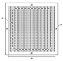
도 2a는 본 발명의 바람직한 실시예에 따른 초접합 VDMOS(20)의 구성에서의 다양한 피쳐들의 배치를 평면도로 나타낸다. 이들 실시예는 n-채널 VDMOS 트랜지스터의 예에 대해 설명될 것이고, (전술한 도 1a 및 1b를 참조하여) 기판 위에 n-타입 에피택셜 실리콘을 성장시킨 n-타입 실리콘 기판에 형성되는 것으로 설명될 것이며; 본 명세서를 참조하는 본 기술분야의 통상의 기술자는 이러한 실시예를 트렌치 게이트 VDMOS 트랜지스터, 비-초접합 VDMOS 디바이스, p-채널 VDMOS 트랜지스터, IGBT 및 수직형 전력 다이오드와 같은 대안적인 타입의 전력 디바이스에 과도한 실험 없이도 용이하게 적용할 수 있을 것으로 당연히 고려된다. 또한, 본 실시예는 개별 전력 디바이스, 즉 집적 회로 다이가 단일 디바이스, 특히 VDMOS(20)와 같은 전력 디바이스를 실현하는 경우에 대해 설명될 것이다. 이러한 의미에서, 다이의 에지에 대한 언급은 적절한 전력 디바이스(예를 들어, VDMOS(20))가 배치되는 반도체 바디의 물리적인 에지를 가리킨다. 물론, 본 실시예 및 그 변형이 부가적인 전력 디바이스, 로직 회로, 아날로그 회로 등과 같은 하나 이상의 액티브 또는 패시브 요소를 포함하는 더 큰 규모의 집적 회로에서 대안적으로 구현될 수 있다는 것이 이해되어야 한다.2A shows a top view of the arrangement of various features in the configuration of a
도 2a의 도면은, VDMOS(20)가 형성되고 있는 다이의 내부를 가로질러 연장되는 평행 "스트라이프(stripe)"의 형태의, VDMOS(20)에서의 p-타입 기둥(24)의 위치를 나타낸다. 이러한 초접합의 경우에, p-타입 기둥(24)은 도 1b와 관련하여 전술한 방식으로 n-타입 에피택셜 층으로(그리고 그와 함께) 형성되며, 이와 같이 에피택셜 층의 n-타입 실리콘이 도 2a의 도면에서 p-타입 기둥들(24) 사이에 존재할 것이다.2A shows the location of the p-
도 2a에 나타낸 바와 같이, 스트라이프 형태인 p-타입 기둥(24) 대신, p-타입 기둥(24) 및 VDMOS(20)의 다른 대응 요소가 "셀"의 어레이로서 배치될 수 있다. 일반적으로 본원에 양도되고 본 명세서에 참고로 통합되는, 2015년 8월 25일자로 허여된 미국 특허 제9,117,899호는 트렌치 게이트 VDMOS 트랜지스터의 경우에 대한 이러한 셀 타입의 기하 구조의 예를 설명한다.2A, other corresponding elements of p-
본 실시예의 이 예에 따르면, 평면 게이트 VDMOS 디바이스에 대해 통상적으로, p-타입 바디 영역이 통상적으로 게이트 아래의 n-타입 에피택셜 영역으로 연장하는 이러한 기둥(24) 내에 형성될 것이며, n+ 소스 영역은 도 1b에 대해 전술한 바와 같이, 이러한 p-타입 바디 영역 내에 후속적으로 형성될 것이다. 이들 p-타입 바디 영역 및 n+ 소스 영역은 본 설명에서 "코어" 영역(22)으로 언급될 다이의 중심 영역 내에 형성될 것이다. 더욱 구체적으로, 본 실시예에서 코어 영역(22)은 전계 산화물과 같은 비교적 두꺼운 절연체 층이 존재하지 않고; 오히려, 게이트 유전체 층과 같은 얇은 산화물이 일반적으로 코어 영역(22) 위에 놓이는 표면의 일부인 VDMOS(20)의 표면의 "기능적으로 액티브인" 영역이다. 도 2a의 코어 영역(22)의 경계는 p-타입 바디 영역, n+ 소스 영역, 및 이러한 바디 및 소스 영역에 대한 컨택이 이러한 경계 내에, 즉 코어 영역(22) 내에 만들어질 수 있도록 하는, 두꺼운 절연체의 에지의 위치를 나타낸다. 반면, 두꺼운 절연체는 코어 영역(22)의 외측에 p-타입 바디 영역 및 n+ 소스 영역의 형성을 방지한다. 도 2b는 전술한 바와 같이 p-타입 기둥(24)(도 2b에서는 명확성을 위해 미도시) 내에 형성되고 통상적으로 그 외부로 연장되는 p-타입 바디 영역(26)의 배치를 나타낸다. 도 2b에 나타내고 전술한 바와 같이, p-타입 바디 영역(26)은 n+ 소스 영역 및 컨택 스트립(도 2b에는 명확성을 위해 미도시)과 같이 코어 영역(22) 내에만 존재한다.According to this example of this embodiment, for a planar gate VDMOS device, a p-type body region will typically be formed in such a
전술한 바와 같이, 본 발명의 실시예는 대안적으로 비-초접합 VDMOS 트랜지스터로 구현될 수 있으며, 이 경우에 기둥(24)은 코어 영역(22)의 내부 또는 외부 어디에도 존재하지 않는다. 비-초접합의 구현에서, p-타입 바디 영역(26)(그리고, 물론 n+ 소스 영역 및 각각에 대한 컨택)은 도 2b에 나타낸 방식으로 코어 영역(22) 내에만 존재한다.As described above, embodiments of the present invention may alternatively be implemented with non-superjumptive VDMOS transistors, in which case the
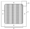
도 2a 및 2b에 나타낸 바와 같이, 종단 영역(25)은 코어 영역(22)의 외측의 VDMOS(20) 부분에 대응하며, 본 예에서는 집적 회로 다이의 에지까지 연장된다. 일부 실시예에서, 후술하는 바와 같이, "전이" 영역은 코어 영역(22)의 에지의 내부에만 존재하는 것으로 고려될 수 있다. 임의의 경우에, 전술한 바와 같이, p-타입 기둥(24)의 일부 단계(instance) 또는 부분이 존재할 수 있거나 코어 영역(22)의 외측으로 그리고 종단 영역(25) 내에서 연장할 수 있지만, 이들 단계에서는 바디 영역(26)이 없을 것이다. 이와 같이, 코어 영역(22)은 VDMOS(20)의 수직 온-상태 소스/드레인 전류를 실질적으로 지원할 것이지만, 온-상태 소스/드레인 전류는 거의 지원되지 않거나 지원되지 않을 것이며, 또는 그렇지 않은 경우 종단 영역(25)으로 전달되거나 통과될 것이다. 오히려, 종단 영역(25)은 인가된 드레인 전압이 나타낼 것인 다이 에지와, 오프-상태에서 VDMOS(20)의 바디 및 소스 영역(그리고 게이트 전극)의 접지 레벨에 있을 것인 코어 영역(22) 사이의 횡방향 전계를 지원하도록 VDMOS(20)에 제공된다.As shown in FIGS. 2A and 2B, the
통상적으로, 종래의 전력 반도체 디바이스에서, 디바이스 종단 영역 및 이러한 종단 영역에 위치한 구조체(즉, 종단 구조체)는 디바이스의 모든 면을 따라 기하학적으로 유사한 방식으로 구성된다. 이 설명의 목적을 위해, "종단 구조체(termination structure)"라는 용어는 디바이스의 기판 및 에피택셜 반도체 바디 내의 도핑 영역의 이러한 부분, 및 종단 영역 내에 있는 반도체 바디의 표면 또는 그 부근의 절연체 및 도전체를 나타낸다. 통상의 수직형 전력 디바이스에서, 한 면으로부터 이웃하는 수직면까지 직사각형 기하 구조(예를 들어, 코어 영역의 외측 에지 또는 종단 영역의 내측 에지)의 코너 위치에서의 전이는 원형 곡선 경로를 따르고, 필수적으로 임의의 지점을 중심으로 고정된 반경으로 에지를 회전시켜 코어 영역의 직선 면을 따라 코너에서 코어 영역과의 동일 거리를 유지한다. 작은-반경의 원형 전이는, 이러한 코너 위치가 디바이스의 항복 거동을 지배하는 경향이 있는 3차원으로 전계를 집중시킬 수 있다는 것이 본 기술분야에 잘 알려져 있다. 이와 같이, 원형 코너를 사용하는 종래의 종단 영역 설계는, 이러한 최악의 경우의 코너에서의 항복 성능이 디바이스 요건을 충족시키는 것을 보장하기 위해 종단 영역이 충분히 넓을 것을 확실하게 해야 한다.Typically, in conventional power semiconductor devices, the device termination region and the structure (i.e., the termination structure) located in such termination region are configured in a geometrically similar manner along all sides of the device. For purposes of this description, the term " termination structure " refers to such portions of the substrate and the doped region in the epitaxial semiconductor body of the device, and the insulator and conductors on or near the surface of the semiconductor body within the termination region . In a typical vertical power device, the transition at a corner position of a rectangular geometry (e.g., the outer edge of the core region or the inner edge of the termination region) from one plane to a neighboring vertical plane follows a circular curve path, The edge is rotated at a fixed radius around an arbitrary point to maintain the same distance from the core region at the corners along the straight surface of the core region. It is well known in the art that small-radius circular transitions can concentrate the electric field in three dimensions where such corner positions tend to dominate the yield behavior of the device. As such, conventional termination zone designs using circular corners must ensure that the termination region is wide enough to ensure that the yield performance at these worst case corners meets the device requirements.
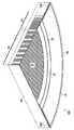
본 발명에 따르면, 모두 원형의 굴곡된 코너를 갖는 디바이스 코어 영역과 종단 영역 구조체의 일반적인 직사각형 배치에서는, 디바이스의 직사각형 코너와 코어 영역 사이에서, 종종 종단 영역의 코너에서의 미사용 영역이 크다. 도 2b는 평행으로부터 집적 회로 다이의 직선 에지로 코어 영역(22)의 면들이 벗어나기 시작하는 위치로부터 연장되는 종단 영역(25)의 그 부분에 대응하는 코너 위치(25C)를 식별한다. 일부 실시예에 따르면, 이러한 달리 미사용된 종단 영역(25)의 코너 위치(25C) 내의, 전계판, 도핑 영역, 절연체 막 및 도전체와 같은 하나 이상의 종단 구조체의 에지는, 전술한 종래의 원형의 굴곡된 에지에 비해 이러한 코너에서 항복 특성을 향상시키도록(즉, 항복 전압을 상승시키도록) 형상과 배치가 설계된다. 더욱 구체적으로, 이들 종단 구조체에 대한 2차의 매끄러운, 비원형 경로(즉, 다양한 국소 곡률 반경의 경로)의 선택은, 이들 에지를 코어 영역(22)의 직선 면을 따르는 것보다 코너 위치에서의 코어 영역(22)으로부터 더 멀리, 다이의 코너에 더 가까이 "신장(stretch)"시키기 위해, 인가된 드레인 전압을 더 긴 거리에 대해 떨어질 수 있게 하여, 애벌런치 항복이 발생하는 전계 아래로 종단 영역(25)에서의 전체 전계를 낮춘다.According to the present invention, in the general rectangular arrangement of the device core region and the end region structure having all the rounded bent corners, there is often a large unused region at the corner of the end region between the rectangular corner of the device and the core region. 2B identifies a
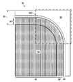
이하, 도 3a 내지 3c를 참조하여, 이러한 초접합 실시예에 따른 VDMOS(20)의 구성을, VDMOS(20)가 실현되는 집적 회로 다이의 코너 위치(25C) 중 하나를 참조하여 상세히 설명할 것이다. 다이의 다른 3개의 코너도 마찬가지로 구성된다는 것이 이해되어야 한다.3A to 3C, the construction of the
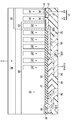
도 3a는 도 2a 및 2b에 나타낸 집적 회로 다이의 상부 우측 코너 위치(25C)에서의 다양한 피쳐들의 레이아웃을 나타내고, 도 3b는 대응 단면이다. 도 3a에서, 일부 피쳐의 부분은, 이러한 부분이 실제 물리적 디바이스에서 반드시 보일 필요는 없지만, 다른 피쳐의 아래에 놓이는 것으로 표시된다. 본 실시예에서, 도 2a 및 2b와 관련하여 전술한 바와 같이, 코어 영역(22)은, 바디 및 소스 영역이 존재하고 컨택 스트립(21)에서 서로 접속되어 VDMOS(20)가 온-상태일 때 소스/드레인 전류가 흐르는 VDMOS(20)의 부분을 포함한다. 이 설명의 목적을 위해, 코어 영역(22)은 도 3b에 나타낸 바와 같이, 전계 산화물(33)과 같은 비교적 두꺼운 절연체 층의 에지에 의해 경계화되는 것으로 고려될 것이다. 본 실시예에서, p-타입 기둥(24)은 전술한 바와 같이, n+ 소스 영역(미도시) 및 p-타입 바디 영역(26)으로 만들어진 컨택(21)과 함께 코어 영역(22) 내에서 스트립으로 배치되고, 본 기술분야에 알려진 바와 같이, 바디 영역(26)에 대한 컨택(21)은 바디 영역(26)에 양호한 저항 접촉을 제공하도록 주입된 p+ 영역(미도시)으로 통상적으로 만들어질 것이다. 도 3b는 p-타입 바디와 n+ 영역이 없어 온-상태 소스/드레인 전류를 지원하지 않는 기둥(24', 24")을 나타낸다. 양쪽 모두 온-상태 소스/드레인 전류를 지원하도록 요구되는 p-타입 바디 및 n+ 영역이 없는 기둥 또는 기둥의 일부를 이하 논-액티브 기둥이라 칭한다. 본 예에서, 논-액티브 기둥(24')은 전계 산화물(33)의 아래에 있지 않고, 코어 영역(22)의 에지에서 "전이" 영역(23) 내에 놓여 있으며, 본 예에서, p-타입 바디 영역(26)(또는, 대안적으로, 게이트 전극 폴리실리콘 개구의 위치)의 위치를 규정하는 마스킹된 주입이 이러한 전이 기둥(24')을 배제시킨다. 논-액티브 기둥(24")은 전계 산화물(33)의 아래에 있고, 이와 같이 종단 영역(25) 내에 있다. 도 3b의 예에서, 기둥(24")이 코어 영역(22)의 경계로부터 종단 영역(25)으로의 경로의 일부만을 연장한다.Figure 3a shows the layout of various features at the upper
본 실시예에서, 폴리실리콘 전계판(32)은 코어 영역(22)의 에지에 제공된다. 폴리실리콘 전계판(32)은 (도 3b에 나타낸 바와 같이) 코어 영역(22) 내의 VDMOS(20)의 게이트 전극(27)과 동일한 폴리실리콘의 레벨로 구성된다. 일부 구현에서, 폴리 전계판(32)은 게이트 전극(27)에 인접하여 전기적으로 접속될 수 있으며; 대안적으로 폴리 전계판(32)은 게이트 전극(27)을 규정하는 폴리실리콘 요소로부터 물리적으로 분리될 수 있다. 코어 영역(22)(전이 영역(23)을 포함)에서, 폴리 전계판(32) 및 게이트 전극(27)은 게이트 유전체(31) 위에 놓이며, 종단 영역(25)에서, 폴리 전계판(32)은 전계 산화물(33) 위에 놓인다. 폴리실리콘 전계판(32)은 코어 영역(22)의 둘레 주위의 모든 코너 및 모든 면에서 인접하게 연장된다.In this embodiment, a
또한, 본 실시예에서, 금속 전계판(34)이 종단 영역(25)에 제공되어, 코어 영역(22) 주위의 모든 코너 및 모든 면에서 인접하게 연장된다. 본 예에서, 금속 전계판(34)은 n-타입 에피택셜 층(42)의 표면의 부근에 있도록 VDMOS(20)에서 금속 도전체의 제1 레벨로 형성되고; 대안적으로, 종단 영역(25)에서 오프-상태 전계에 대해 원하는 오프-상태 효과가 얻어지는 한 더 높은 금속 레벨로 형성될 수 있다. 도 3a 및 3b에 나타낸 바와 같이, 금속 전계판(34)은 내측 에지(34Ei)까지 폴리 전계판(32) 위에 놓여 있고, 폴리 전계판(32)의 외부 에지(32EO)를 넘어 종단 영역(25)으로 연장된다. 본 예에서, 금속 전계판(34)은, 이를 통해 컨택(35)이 형성되어 금속 전계판(34)을 폴리 전계판(32)에 접속시키는 레벨간(interlevel) 유전체(41)에 의해 통상의 방식으로 폴리 전계판(32)으로부터 분리된다.In addition, in this embodiment, a
본 실시예에서, 금속 전계판(34) 및 그에 따른 폴리 전계판(32)은 오프 상태에서 드레인 전압에 비해 낮은 전압을 수신한다. 폴리 전계판(32)이 코어 영역(22)에서 게이트 전극(27)에 인접하거나 다른 방식으로 접속되어 있는 경우, 게이트 전압 G가 금속 전계판(34)에 인가되어 코어 영역(22)에서 VDMOS(20)에 의한 전도를 제어할 수 있다. 대안적으로, 폴리 전계판(32)이 게이트 전극(27)에 접속되지 않은 경우, 소스 전압 S(즉, 접지 전위)가 금속 전계판(34)에 인가될 수 있다.In this embodiment, the
종단 영역(25)은, VDMOS(20)가 실현되는 집적 회로 다이의 에지(20E)까지 전계판(32, 34)의 외부로 연장된다. 기판(40) 위에 놓인 N-타입 에피택셜 층(42)은 코어 영역(22)으로부터 논-액티브 p-타입 기둥(24")의 위치를 넘어, 종단 영역(25)의 외부 부분에서의 전계 산화물(33) 아래의 표면에 존재한다. 에피택셜 층(42)의 표면의 액티브 영역(38)은 다이 에지(20E) 부근에서 노출된다. 본 실시예에서, 고전압 금속 도전체(36)가 코어 영역(22) 주위의 모든 면 및 모든 코너 및 다이의 외주 부근에서 많은 종단 영역(25)에 인접하게 연장된다. 금속 도전체(36)는 컨택(39)에서 액티브 영역(38)과 접촉하고, 다이 주변으로부터 종단 영역(25)으로 내측으로 연장되고, 전계 산화물(33)의 외부 부분의 위에 놓인다.The
전술한 바와 같이, VDMOS(20)가 오프 상태에 있을 때, 코어 영역(22)은 디바이스 소스 및 바디 영역과 게이트 전극의 저전압(접지) 전위에서 완전히 공핍되며, 고전압 액티브 영역(38)(및 기판(40))이 수백 볼트만큼 높을 수 있는, 인가된 드레인 전압에 있을 것이다. 이들 전위는 고전압 액티브 영역(38)과 공핍 코어 영역(22) 사이에서 횡방향으로 전계를 확립한다. VDMOS(20)가 오프 상태에 있으면, 폴리 전계판(32) 및 금속 전계판(34)은 액티브 코어 영역(22)의 외측에서 종단 영역(25) 내의 저전압 등전위 표면 및 구조체로서의 역할을 하며, 고전압 금속 도전체(36)는 다이 에지(20E)로부터 종단 영역(25)으로 연장하는 높은 전압 등전위면을 제공한다. 이러한 등전위면의 토폴로지, 형상 및 특성은, VDMOS(20)가 오프될 때 종단 영역(25)에서의 전계를 제어하는 역할을 할 것이다. 더욱 구체적으로, 종단 영역(25)의 코너 위치(25C)에서의 전계판(32, 34), 고전압 도전체(36) 및 액티브 영역(38)의 에지의 형상 및 배치는 VDMOS(20)의 항복 성능을 향상시키기 위하여 이러한 코너의 추가 영역을 이용한다. 이러한 개선은 이러한 에지에 대한 2차의 매끄러운 비원형 경로의 선택에 의해 달성되고, 따라서 대응하는 종단 구조체가 통상의 설계에 비해 더 긴 거리에 걸쳐 코어 영역(22)에서 접지 전위에 대한 드레인 전압을 강하시키며, 반도체에 대한 임계 전계 아래에서 전계 강도를 유지한다.When the
도 3a에 나타낸 실시예에서, 에지(33E)는 본 설명의 목적을 위해 코어 영역(22)의 외부 에지를 확립하는 전계 산화물(33)의 내부 에지이다(종단 구조체의 본 설명에서, "내부", "외부", "내측" 및 "외측"과 같은 방향 용어는 코어 영역(22)에 대해 상대적임). 폴리 전계판(32)의 외부 에지(32E0)는 전계 산화물 에지(33E)의 외측에 위치하며, 금속 전계판(34)의 내부 에지(34Ei)는 전계 산화물 에지(33E)의 외측 및 폴리 전계판(32)의 외부 에지(32E0)의 내측에 위치한다. 금속 전계판(34)의 외부 에지(34E0)는 폴리 전계판(32)의 외부 에지(32E0)의 외측에 위치한다. 고전압 도전체(36)는 금속 전계판(34)의 외부 에지(34E0)의 외측에 위치한 내부 에지(36E)를 갖고, 액티브 영역(38)은 고전압 도전체(36)의 내부 에지(36E)의 외측에 위치한 내부 에지(38E)를 갖는다. 고전압 도전체(36) 및 액티브 영역(38)의 외부 에지의 위치는 본 실시예에서 오프-상태 전계를 제어하는 데 특히 중요하지는 않다.In the embodiment shown in Figure 3A, the
도 3c는 두꺼운 산화물(37)이 종단 영역(25)에 형성되는 VDMOS(20)의 종단 영역(25)의 대안적인 배치를 나타내고, 그 외부 에지(34E0)를 포함하는 금속 전계판(34)의 외부 부분은 두꺼운 산화물(37) 위로 연장된다. 이 배치에서의 다른 피쳐는 도 3b와 관련하여 전술한 바와 동일하다. 본 실시예에 따르면, 두꺼운 산화물(37)은 또한 그 위치가 금속 전계판(34, 36)의 높이, 그에 따라 종단 영역(25)에서의 전계의 형상에 영향을 준다는 점에서 종단 구조체로 고려된다. 따라서, 두꺼운 산화물(37)의 내부 에지(37Ei) 및 외부 에지(37E0)의 형상 및 배치는, 본 구현에서, 본 실시예에 따른 VDMOS(20)의 항복 성능을 향상시키기 위해, 다이의 코너에서의 추가 영역을 이용하도록 설계될 수 있다.3C shows an alternative arrangement of the
종단 영역(25) 내의 종단 구조체 에지의 이상적인 최적화된 설계는, 종단 영역(25) 내의 도전체와 유전체의 기하학적 배치를 고려하여 종단 영역(25C)의 내부 에지(전계 산화물 에지(33E)) 및 외부 에지(액티브 영역 에지(38E))에서 오프-상태 전위를 확립하는 이러한 디바이스 도전체 및 영역의 기하학적 배치의 경계 조건에 적용되는 (정전기학에 대한) 푸아송(Poisson) 방정식의 솔루션을 따를 것이다. 본 기술 분야에 알려진 바와 같이, 물리적 원리 및 대응하는 수학적 유도는 푸아송 방정식에 대한 솔루션이 수학적 관점에서 분석적이고 2차 매끄러움을 가질 것을 요구한다. 본 실시예에 따르면, 종단 영역(25) 내의 전위 및 전계를 형성하고 규정하는 종단 구조체 에지는 국소 곡률 반경이 변하는, 분석적이고 2차의 매끄러운 곡선에 적어도 근접하게 근사되는 형상을 갖는다. 이러한 특성은, 애벌런치 항복의 시작으로 귀결되는, 반도체에 대한 임계 전계 위에 오프-상태 전계를 국부적으로 집중시킬 수 있는 "뒤틀림(kink)" 또는 급격한 변화가 없음을 보장한다.The ideal optimized design of the edge of the termination structure within the
복잡한 기하 영역 내의 푸아송의 방정식에 대한 솔루션은, 알려진 단순한 기하학 솔루션을 취하고, 새로운 영역에 맞도록 등각 맵에 의한 솔루션을 "신장"시킴으로써 종종 도달될 수 있다는 것이 수학 원리에서 잘 알려져 있다. 일 실시예에 따르면, 전계판(32, 34), 고전압 도전체(36), 액티브 영역(38) 및 전계 산화물(33)과 두꺼운 산화물(37)과 같은 절연층의 에지의 기하학적 에지를 통상의 일정-반경 또는 "원형" 코너 기하 형태에 비해 종단 영역(25)의 코너 위치(25C)로 더 깊게 "신장"시키고, 그에 대응하여 VDMOS(20) 내의 오프-상태 등전위 라인을 다이의 코너로 대응하여 신장시키고 그 결과 코너 위치(25C) 내의 전계를 낮추는, 이러한 방식으로 등각 맵이 적용된다. 이러한 등각 맵 접근법은 종단 영역(25)에서 전계의 이상적으로 최적의 성형을 제공하고, 그에 따라 주어진 드레인 전압 레벨에 대해 종단 영역(25)에 의해 소비되는 칩 면적을 최적화할 수 있다.It is well known in mathematical principles that the solution to Poisson's equation in a complex geometry region can often be reached by taking a known simple geometry solution and "stretching" the solution by conforming maps to fit the new domain. According to one embodiment, the geometric edges of the edges of the insulating layers, such as the
이들 실시예에 따르면, 종단 영역에서의 구조체의 이상적인 최적화된 에지가 항복 성능의 상당한 개선을 달성하기 위해 정확하게 필요하지는 않다는 것도 관찰되었다. 오히려, 전계에 바람직하지 않은 국부 뒤틀림을 도입하지 않도록, 종단 영역(25)의 코너 위치(25C)에서 종단 구조체 에지를 신장시키는 수학적 함수를 사용함으로써, 등각 매핑 솔루션(conformally mapped solution)의 근접 근사가 실질적인 의미에서 용이하게 도출될 수 있다는 것이 밝혀졌다. 일 실시예에 따르면, 이러한 타입의 신장에 대해 선택된 수학 툴은, 2차 매끄러운 분석 함수의 정의에 의한 3차 이상 베지어 곡선이다.It has also been observed, according to these embodiments, that the ideal optimized edge of the structure in the termination region is not exactly required to achieve a significant improvement in yield performance. Rather, by using a mathematical function to stretch the edge of the structure at the
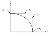
본 실시예에 적용된 베지어 곡선의 일례는 원하는 최적 경로를 근사하도록 선택된 대응 제어점을 갖는 3차 다항식(즉, 큐빅) 베지어 곡선이다. 도 4a는 데카르트 평면의 1사분면에서 단위 원으로 매핑되고, 도 3a의 코너 위치(25C)에 적용될 수 있는 간단한 큐빅 베지어 곡선을 나타낸다. 이 예에서는, 4개의 제어점, P0 내지 P3이 선택된다. 제어점 P0 및 P3은 경로의 종점에 있으며, 본 실시예에 따른 종단 구조체와 관련하여 코너 위치(25C)에 진입할 때 에지가 그 직선면으로부터 벗어나기 시작하는 점이 될 것이다. 본 기술분야에서 베지어 곡선에 대해 알려진 바와 같이, 4개의 제어점은 다음과 같다:An example of a Bezier curve applied to this embodiment is a cubic polynomial (i.e. cubic) Bezier curve with corresponding control points selected to approximate the desired optimal path. Figure 4A shows a simple cubic Bezier curve that maps to a unit circle in the first quadrant of the Cartesian plane and can be applied to the
P0 : x0, y0 = (0, 1) // 경로의 개시점P 0 : x 0 , y 0 = (0, 1) // Starting point of the path
P1 : x1, y1 = (s, 1) // P0-P1은 경로가 P0을 떠나는 각도를 설정P 1 : x 1 , y 1 = (s, 1) // P 0 -P 1 sets the angle at which the path leaves P 0
P2 : x2, y2 = (1, s) // P2-P3은 경로가 P3에 진입하는 각도를 설정P 2 : x 2 , y 2 = (1, s) // P 2 -P 3 sets the angle at which the path enters P 3
P3 : x3, y3 = (l, 0) // 경로의 종점P 3 : x 3 , y 3 = (l, 0) // end point of the path
도 4a의 예에서, 통상적으로 이러한 실시예에 적용되는 바와 같이, 베지어 곡선은 그 중간점을 통해 축에 대해 대칭이 될 것이라는 점에서 "규칙적"이 될 것이다. 제어점 P0 내지 P3의 선택에 후속하여, 곡선은 0과 1 사이에서 연속적으로 변하는 t의 파라미터화이다.In the example of FIG. 4A, the Bezier curve will be " regular " in that it will be symmetrical about the axis through its midpoint, as is typically applied to this embodiment. Following the selection of control points P 0 to P 3 , the curve is a parameterization of t that changes continuously between 0 and 1.
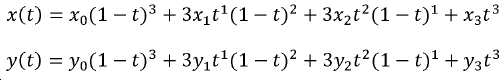
파라미터 s는 점 P2를 향해 (그리고 제어점 P2 및 P3에 대해 유사하게) 떨어지기 전에, 제어점 P0에서 P1까지 곡선이 얼마나 멀리 이동하는지를 결정한다는 점에서 스케일링 팩터로 볼 수 있다. 스케일링 파라미터 ![]()
![]()
![]()
![]()
차단 전계를 형성하는데 바람직하다면, 종단 구조체 에지가 VDMOS(20)의 4면 모두에서 대칭일 필요는 없음을 고려하여, 이들 실시예에 적용되는 큐빅 베지어 곡선에 추가의 자유도가 통합되어 높이 a에서 y-축 상의 구조를 변환하여 원점으로부터의 거리 b에서 x-축 상의 구조에 매칭시킬 수 있다. 이 경우, 베지어 곡선 공식은 (큐빅 경우에 대해) 제어점 P0 내지 P3의 상이한 세트를 채용하도록 변형될 것이다.If desired to form the block field, the termination structure edges in consideration of symmetry one need not at all four sides of the VDMOS (20), an additional degree of freedom is incorporated in the curve built cubic chopping to be applied to the examples in the height of a The structure on the y-axis can be transformed and matched to the structure on the x-axis at a distance b from the origin. In this case, the Bezier curve formulation will be modified to employ a different set of control points P 0 to P 3 (for cubic cases).
P0 : x0, y0 = (0, a) // 경로의 개시점P 0 : x 0 , y 0 = (0, a) // start point of the path
P1 : x1, y1 = (s1, a) // P1-P2는 경로가 P1을 떠나는 각도를 설정P 1 : x 1 , y 1 = (s 1, a) // P 1 -P 2 sets the angle at which the path leaves P 1
P2 : x2, y2 = (b, s2) // P2-P3는 경로가 P3에 진입하는 각도를 설정P 2 : x 2 , y 2 = (b, s 2) // P 2 -P 3 sets the angle at which the path enters P 3
P3 : x3, y3 = (b, 0) // 경로의 종점P 3 : x 3 , y 3 = (b, 0) // end point of the path
이 경우, 2개의 스케일링 팩터 s1, s2는 원형 경로로부터 외부로 경로의 형상을 비대칭으로 신장시키는 값을 갖도록 선택될 것이다. 경로가 곡률을 변경하는 속도는 이 접근법에서 서로 다를 팩터 s1, s2에 의해 결정된다. 도 4b는 이러한 대안적인 구현에 따른 비대칭 큐빅 베지어 곡선의 예를 나타낸다.In this case, the two scaling factors s1, s2 will be selected to have a value that asymmetrically stretches the shape of the path from the circular path to the outside. The rate at which the path changes curvature is determined by the different factors s1, s2 in this approach. Figure 4b shows an example of an asymmetric cubic Bezier curve according to this alternative implementation.
VDMOS(20)의 코너 위치(25C) 내의 종단 구조체의 배치에 적용되는 이러한 구현들 중 임의의 구현에서, 이러한 실시예에 따른 베지어 곡선의 사용은, 그렇지 않으면 전계를 왜곡시키지 않고 접속하는 것이 곤란한 종단 영역(25)의 이종 영역을 함께 스티칭(stiching)하는 것을 편리하게 한다.In any of these implementations that are applied to the placement of the termination structure within the
도 3a 내지 도 3c에 나타낸 실시예에 따르면, 종단 구조체의 에지들 중 몇몇은 실질적으로 큐빅 베지어 곡선에 따라 신장된다. 이 설명의 목적을 위해, 특정 곡선을 따르는 것을 언급할 때, "실질적으로"이라는 용어는 특정의 수학적 함수에 대응하는 경로를 완벽하게 따르지는 않을 수 있지만 이러한 실시예의 맥락 내에서, 그 함수를 완벽하게 따른 이러한 구조체와 유사하게 거동하도록 충분히 근접하는 구조체를 가리킨다. 구체적으로, 본 실시예에서, 폴리 전계판(32)의 외부 에지(32E0), 금속 전계판(34)의 내부 에지(34Ei) 및 외부 에지(34E0), 고전압 도전체(36)의 내부 에지(36E) 및 액티브 영역(38)의 내부 에지(38E)의 각각은 도 3a 및 3b의 예에서 각각의 큐빅 베지어 곡선에 따라 실질적으로 신장되며; 도 3c의 예에서, 두꺼운 산화물(37)의 내부 에지(37Ei) 및 외부 에지(37E0)는 또한 각각의 큐빅 베지어 곡선에 따라 실질적으로 신장될 수 있다.According to the embodiment shown in FIGS. 3A-3C, some of the edges of the termination structure extend substantially along the cubic Bezier curve. For purposes of this description, when referring to following a particular curve, the term " substantially " may not perfectly follow the path corresponding to a particular mathematical function, but within the context of this embodiment, Lt; RTI ID = 0.0 > close < / RTI > Specifically, in this embodiment, the
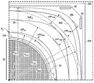
본 실시예에 따른 종단 구조체 에지의 형상 및 배치를 통상의 원형 설계의 형상 및 배치와 비교하는 것이 유용하다. 이와 관련하여, 도 3a 및 3b의 구조체에서, 도 3d는 종래의 원형 배치에 따라 폴리 전계판(32)의 외부 에지를 규정하는 일정한 반경 REP1의 원형 경로를 나타낸다. 이 반경 RFP1은 코어 영역(22)의 직선 면을 따라, 그리고 코너 위치(25c) 양쪽에서 폴리 전계판(32)의 외부 에지와 코어 영역(22)의 경계(즉, 도 3a의 전계 산화물 에지(33E)) 사이의 동일한 거리를 유지하는 원의 반경에 대응한다. 외부 에지(32E0)가 코어 영역(22)의 직선 면을 따라 코어 영역(22)의 경계로부터 거리를 둔 점 P0 및 P3으로부터 큐빅 베지어 곡선을 실질적으로 따르는 본 실시예에 따르면, 스케일링 팩터 s는 원형값 ![]()
![]()
![]()
![]()
도 3d는 금속 전계판(34)의 외부 에지(34E0), 고전압 도전체(36)의 내부 에지(36E) 및 액티브 영역(38)의 내부 에지(38E)에 대한 유사한 비교를 나타내며, 이들 각각은 원형값 ![]()
![]()
![]()
![]()
종단 영역(25)에서의 다른 종단 구조체가 유사하게 본 실시예에 따라 형성될 수 있다. 예를 들어, 도 3c를 참조하면, 두꺼운 산화물(37)의 에지가 또한 코너 위치(25C)에서 2차의 매끄러운 비원형 경로를 따라 실질적으로 신장될 수 있다. 이러한 배치는, 두꺼운 산화물(37)이 금속 전계판(34)과 에피택셜 층(42)의 아래에 놓인 반도체 사이의 거리의 팩터라는 것을 고려하여, 종단 영역(25)의 전계에 약간의 영향을 미칠 것이다.Other termination structures in the
도 3e는 본 실시예에 따른 종단 영역 코너 위치(25C)로 신장된 에지를 갖는 다른 유형의 종단 구조체를 나타낸다. 이 예에서, 코너 위치(25C) 내의 p-타입 기둥(24, 24")의 단부는 실질적으로 큐빅 베지어 곡선에 따라, 보다 구체적으로는 도 4b에 대해 전술한 바와 같이 상이한 스케일링 팩터 s1, s2를 갖는 비대칭 큐빅 베지어 곡선에 따라 코너로 신장되는 경로 또는 "에지"(24E)를 규정한다. 에지(24E)는 코너 위치(25C)의 외측에서 코어 영역(22)의 면과 평행하게, 예를 들면, 도 3e에 나타낸 바와 같이, 코어 영역(22)의 이러한 면을 따라, 또는 코어 영역(22)의 다른 면을 따라 종단 영역(25)으로 연장되는 기둥(24)의 종점을 따라 최 외각 기둥(24")과 평행하게 연장됨으로써 연장되는 것으로 고려될 수 있다. 전계판, 고전압 도전체 및 영역, 절연체 막 등과 같은 다른 종단 구조체가 또한 코너 위치(25C) 내에서 종단 영역(25)의 코너로 신장된 에지를 가질 수 있지만, 명확성을 위해 도 3e에는 나타내지 않았다. 종단 영역(25) 내의 p-타입 기둥(24, 24")으로 구성된 도핑 영역은 또한 코어 영역(22)과 다이의 에지를 향한 고전압 요소 사이의 전계에 영향을 미치고, 따라서 이러한 기둥(24, 24")의 종점에 의해 규정되는 "에지"(24E)의 코너로의 신장은 또한 본 구현에서 VDMOS(20)의 항복 특성을 향상시키기 위해 그 전계를 제어할 수 있다.3E shows another type of end structure having an edge elongated to an end
전술한 바와 같이, 그리고 본 기술분야에 알려진 바와 같이, 정전 푸아송 방정식에 대한 솔루션은, 전계 강도가 관련 도전체의 날카로운 기하학적 코너(즉, 더 작은 국소 곡률 반경)에서 강화된다는 것을 나타낸다. 예를 들어, 도 3a 및 3d에 나타낸 실시예를 참조하면, 각 에지(32E0, 34E0, 36E, 38E)의 국소 곡률 반경은 코어 영역(22)의 직선 면으로부터 코너 위치(25C)로의 더욱 먼 점들에서 감소하고, 사실상 이들 에지가 각각 일정한 반경 RFP2, RHV1, RHV2에 비해 그 각각의 최대 증가 거리 ![]()
![]()
![]()
![]()
본 실시예에 따르면, 종단 구조체 에지의 형상 및 배치의 신장은 그에 따라 종단 영역(25)이 전력 VDMOS(20)의 오프-상태 드레인-대-소스 전압을 횡방향으로 지원하는 능력을 현저하게 향상시킬 수 있다. 이러한 개선, 및 VDMOS(20)가 실현되는 집적 회로 다이의 코너에서의 그렇지 않으면 낭비되는 칩 영역의 사용은 전력 VDMOS(20)의 단위 면적당 전달되는 전류의 관점에서 개선된 효율로 귀결될 수 있다.According to the present embodiment, the configuration and extension of the configuration of the edge of the structure allows the
본 실시예에 대한 다양한 대안 및 변형이 고려된다. 이러한 대안 중 하나에 따르면, 다이 코너를 향한 종단 구조체 에지의 이러한 신장에 의해 제공되는, 감소되고 제어된 전계는, 예를 들어, 전이 영역(23) 및 그 논-액티브 기둥(24')에 대한 필요성을 감소시키거나 심지어 제거할 수 있는, 전계 산화물(33)을 코어 영역(22)의 중심을 향하여 더 이동시킴으로써, 종단 영역(25)이 코어 영역(22)의 액티브 요소에 더 가깝게 배치되게 할 수 있다. 전계 산화물 에지(33E)의 이러한 배치는, 코어 영역(22)과 고전압 액티브 영역(38) 사이에서 전위가 강하되는 거리를 추가로 연장시켜, 종단 영역(25)에서의 전계의 강도를 낮출 것이다.Various alternatives and modifications to this embodiment are contemplated. According to one of these alternatives, a reduced and controlled electric field provided by this extension of the edge of the end structure towards the die corner can be achieved, for example, for the
또 다른 대안에 따르면, 다이 코너를 향한 종단 구조체 에지의 신장은, 코어 영역(22)의 경계(즉, 도 3a 내지 3c의 실시예에서 전계 산화물 에지(33E))를 다이의 코너로 더 멀리 이동시키는 것을 허용할 수 있다. 예를 들어, 전계 산화물 에지(33E)는 또한, 전체 집적 회로 디바이스의 크기를 일정하게 유지하면서, 코어 영역(22)의 크기를 증가시키고, 그에 따라 디바이스의 구동 전류를 증가시키도록 실질적으로 2차의 매끄럽고 비원형의 경로를 따라 성형되어 배치될 수 있다.According to yet another alternative, the elongation of the end structure edge towards the die corner causes the boundary of the core region 22 (i.e., the
다른 대안 및 변형은 비-초접합 타입의 수직형 MOSFET, IGBT, 수직형 전력 다이오드 등과 같은 전력 디바이스에서 이러한 방식으로 종단 구조체 에지를 신장시키는 것을 포함한다. 본 명세서를 참조하는 본 기술분야의 통상의 기술자에게 명백할 것인 이러한 대안 및 변형은 이하 청구되는 본 발명의 범위 내에 속하는 것으로 고려된다.Other alternatives and variations include extending the structure edges in this manner in power devices such as non-superjunction type vertical MOSFETs, IGBTs, vertical power diodes, and the like. These alternatives and modifications, which will be apparent to those of ordinary skill in the art having reference to this disclosure, are considered to be within the scope of the invention as hereinafter claimed.
초접합 전력 MOSFET 디바이스의 표면으로부터 연장되는 교번하는 n-타입 및 p-타입 도핑된 기둥은 필연적으로 기생 사이리스터 또는 SCR 디바이스의 가능성을 제시한다. 도 3b 및 3c와 관련하여 전술한 바와 같이, 논-액티브 p-타입 기둥을 갖는 종단 영역을 포함하는 이러한 디바이스에서, 이들 논-액티브 기둥은, 소스 전위에 하드 와이어링되지 않았거나 다른 방식으로 디바이스의 정상적으로 바이어싱된 노드에 물리적으로 접속되지 않았다는 점에서 부유되며, 또는 기둥의 논-액티브 부분의 경우에, 이들은 p-타입 기둥 자체의 액티브 부분을 통해 소스 전위에 약하게 전기적으로 접속된다; 그러나, 기둥의 이러한 약하게 접속된 논-액티브 부분은, 드레인 전위가 증가함에 따라 기둥의 약하게 접속된 부분이 자유 캐리어가 점점 공핍될 수 있게 하여 기둥의 액티브 부분으로부터 전기적으로 접속 해제된다. 결과적으로, 이러한 논-액티브 부유 또는 약하게 접속된 도핑 영역은 디바이스의 액티브 코어 영역을 포함하여 인접한 기둥으로부터 국부적으로 바이어스되기 쉽다. 이러한 국소 바이어싱이 기생 n-p-n-p SCR 디바이스 구조체를 트리거링하기에 충분히 커지면, 높은 누설 전류와 디바이스 항복이, 초접합 깊이 및 종단 영역 설계에 기초하여 그렇지 않은 경우 예상되는 것보다 훨씬 낮은 전압에서 발생할 것이다.Alternating n-type and p-type doped pillars extending from the surface of the superjunction power MOSFET device inevitably present the possibility of parasitic thyristor or SCR devices. In such devices, which include termination regions with non-active p-type columns, as discussed above in connection with Figures 3b and 3c, these non-active columns are not hard wired to the source potential, In the case of the non-active portions of the pillars, they are weakly electrically connected to the source potential through the active portion of the p-type column itself; This weakly connected non-active portion of the column, however, is electrically disconnected from the active portion of the column by allowing the weakly connected portion of the column to gradually deplete the free carrier as the drain potential increases. As a result, such non-active floating or weakly connected doped regions tend to be locally biased from adjacent pillars including the active core region of the device. If such local biasing is large enough to trigger a parasitic n-p-n-p SCR device structure, high leakage current and device yield will occur at voltages well below what would otherwise be expected based on the superjunction depth and termination area design.
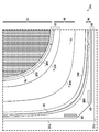
또 다른 실시예에 따르면, 수직형 초접합 반도체 디바이스의 종단 영역은, 그 디바이스의 종단 영역의 외부 에지 부근에 위치하고, 기생 SCR 구조체를 구성하는 도핑 영역을 둘러싸는 하나 이상의 전기적 부유 도핑 영역에 의해 그 타입의 장치에 내재된 기생 SCR 구조체의 기생 누설 및 트리거링을 억제하도록 구성된다. 이들 부유 도핑 영역 또는 가드 링은 이하 설명되는 바와 같이, 디바이스의 표면 위에서 볼 때 하나 이상의 동심 링으로서 2차원으로 보일 것이다.According to yet another embodiment, the termination region of the vertical type superconducting semiconductor device is formed by at least one electrically floating doping region located near the outer edge of the termination region of the device and surrounding the doping region constituting the parasitic SCR structure. Lt; RTI ID = 0.0 > and / or < / RTI > parasitic SCR structures inherent in the device. These floating doped regions or guard rings will look two-dimensionally as one or more concentric rings when viewed from above the surface of the device, as will be described below.
도 5a는 VDMOS 트랜지스터(50), 예를 들어 위에 놓인 n-타입 에피택셜 층을 갖는 n-타입 실리콘 기판에 형성된 n-채널 VDMOS 트랜지스터를 나타낸다. 물론, VDMOS(50)는 대안적으로 p-채널 VDMOS 트랜지스터로서 형성될 수 있으며, 이 경우 그 다양한 요소들의 도전 타입이 본 설명의 도전 타입과는 반대일 것이다. 도 2a에 나타낸 실시예에 대해 전술한 것과 유사한 방식으로, 평행 스트라이프 형태의 p-타입 기둥(54)이, VDMOS(50)가 실현되는 집적 회로 다이의 내부를 가로질러 연장되며, 전술한 바와 같이 n-타입 에피택셜 층으로 연장하여, 도 5a의 도면에서 n-타입 에피택셜 실리콘이 인접한 p-타입 기둥들(54) 사이에 존재할 것이다. 그리고, 전술한 바와 같이, p-타입 기둥(54) 및 VDMOS(50)의 다른 대응하는 요소가 대안적으로 "셀"의 어레이로서 배열될 수 있다.5A shows a
도 5a에 경계가 정해진 코어 영역(52)은, p-타입 바디 영역, n+ 소스 영역 및 컨택이 이러한 기둥(54) 내에 형성되고, 이러한 n-채널 구현에서 접지 전위(Vss)로 바이어싱될 집적 회로 다이의 부분을 나타낸다. 전술한 바와 같이, 도 5a에 나타낸 코어 영역(52)의 경계는 도 3b 및 3c의 실시예에서 전계 산화물(33)과 같은 절연 유전체 막의 내부 에지의 위치에 대응한다. 전술한 바와 유사하게, 도 5a에 나타낸 종단 영역(55)은 코어 영역(52)의 외측의 다이의 그 부분이다. 도 3a 내지 3d와 관련하여 전술한 바와 같은 구조체가 이 종단 영역(55) 내에 제공되어 오프-상태에서 VDMOS(50)에 인가되는 드레인-대 소스 전압을 횡방향으로 지원할 수 있다. 이와 관련하여, 전체적으로 코어 영역(52)의 외측에 있는 기둥(54)뿐만 아니라 코어 영역(52)의 외측에 있는 기둥(54)의 부분은 전술한 바와 같이 오프-상태에서 소스 전압에서 능동적으로 바이어싱되지 않을 것이지만, 전술한 바와 같이 종단 영역(55)의 전계에 영향을 줄 것이다.5A, a p-type body region, an n + source region, and a contact are formed in this
도 5a에 나타낸 본 실시예에서, 전기적 부유 가드 링(60)은 종단 영역(55) 내에 배치되고 VDMOS(50)의 병렬 p-타입 기둥(54)을 둘러싸고 있다. 이 n-채널 수직형 MOSFET 구현에서, 가드 링(60)은 n-타입 에피택셜 층 내로 형성된 인접하는 p-타입 도핑 영역이다. 더욱 상세하게 후술하는 바와 같이, 가드 링(60)은 n-타입 실리콘의 에피택시 중에 형성된 p-타입 기둥(54)의 마지막 세그먼트들 중 하나 이상으로서 동시에 형성될 수 있으며, 이 경우에 가드 링(60)은 이들 세그먼트와 동일한 깊이, 폭 및 도펀트 농도를 가질 것이며, 도핑된 재료의 3차원 벽(이 예에서는 p-타입)을 형성할 것이다. 일부 구현에서, 가드 링(60)은 p-타입 기둥(54)의 전체 깊이까지 연장될 수 있다. 대안적으로, 가드 링(60)의 깊이, 형성 및 도펀트 농도는 p-타입 기둥(54)과 다를 수 있으며, 예를 들어, 전계 산화물의 형성 전에 n-타입 에피택셜 층으로의 마스킹된 이온 주입에 의해 형성될 때 최상부의 초접합 기둥 세그먼트의 깊이를 부분적으로 갖는다. 예를 들어, 가드 링(60)은 현재의 기술에 따른 수직형 초접합 MOSFET 구현에 대해 약 10 ㎛ 내지 약 100 ㎛ 정도의 범위에서 통상의 깊이를 가질 수 있다.5A, an electrical floating
도 5b는 종단 영역(55) 내에 전계판을 형성하기 이전의 제조 단계에서, VDMOS(50)의 코너 위치(55C) 부근에 가드 링(60)을 배치한 예를 나타낸다. 가드 링(60)은 코어 영역(52)과 종단 영역(55) 내에 논-액티브 기둥(및 기둥의 논-액티브 부분)(54')을 둘러싸고, 다이의 에지에서 액티브 영역(58)의 내측에 배치된다. 원하는 경우, 가드 링(60)은 액티브 영역(58)과 접촉하는 고전압 도전체의 아래에 놓일 수 있다. 도 5b의 도면에서, 가드 링(60)의 수직 연장 부분은 이들 논-액티브 기둥(54')과 평행하며, 인접 기둥(54, 54')의 간격과 동일한 간격만큼 최외각 논-액티브 기둥(54')으로부터 이격되어 포토리소그래피 규칙성을 유지한다. 코어 영역(52)의 다른 면상에, (도 5b의 도면에서) 가드 링(60)의 수평으로 연장하는 부분은 대략 동일한 간격으로 논-액티브 기둥 부분(54')의 단부와 평행하다. 대안적으로, 가드 링(60)과 기둥(54') 사이의 간격은 기둥들(54, 54') 자체 사이의 간격과 다를 수 있으며, 이는 종단 영역(55)에서 오프-상태 전계를 제어하는데 유용할 수 있다.5B shows an example in which the
도 6a 및 6b는, 가드 링(60)이 VDMOS(50)의 n-타입 에피택셜 층(62)으로 연장될 수 있는 깊이의 변화를 나타낸다. 도 6a에 나타낸 VDMOS(50a)의 절단도는 도 3a 내지 3c와 관련하여 전술한 종단 구조체와 유사한 특정의 종단 구조체를 나타낸다. 이들 종단 구조체는 폴리 전계판(64), 금속 전계판(66), 두꺼운 산화물(67) 및 고전압 도전체(68)를 포함한다. 도 6a의 VDMOS(50a)는 초접합 타입이며, 이와 같이 p-타입 기둥(54, 54')이, n-타입 에피택셜 층(62)에 매우 깊이 연장되는 깊이까지 형성되며, 예를 들어, 복수 공정의 에피택셜 프로세스 형성층(62)의 각 공정 후에 복수의 주입에 의해 형성된다. 본 예에서, p-타입 가드 링(60a)은 기둥의 깊이와 유사한 깊이를 가지며, 이와 같이 n-타입 층(62)의 에피택시 중에 기둥(54, 54')과 유사한 방식으로 형성될 수 있다. 도 6a에 나타낸 VDMOS(50a)의 예에서, 가드 링(60a)은 인접한 바디 영역들(54, 54') 사이의 간격보다 최외각 논-액티브 바디 영역(54')으로부터 더 멀리 이격되어 있다.6A and 6B show a variation in depth where the
도 6b는, p-타입 가드 링(60b)이 초접합 기둥들(54, 54')보다 훨씬 더 얕은 깊이를 갖는 초접합 VDMOS(50b)의 구성을 나타낸다. 이 구현에서, 가드 링(60b)은 n-타입 에피택셜 층(62)이 완전히 형성된 후에, 그리고 종단 영역(55)에서 전계 산화물의 퇴적 또는 열 성장 이전에 마스킹된 이온 주입에 의해 형성된다. 대안적으로, 가드 링(60b)은 예를 들어 초접합 기둥들(54, 54')의 최상부의 하나 이상의 세그먼트와 함께 주입되어 에피택셜 층(62)으로 부분적으로 연장될 수 있다.6B shows the configuration of the
본 실시예에 따르면, 가드 링(60a, 60b)은 VDMOS(50)의 오프-상태에서 능동적으로 바이어싱되지 않고, 오히려 전기적으로 부유 상태로 남아 있다. 이것은 통상적으로 접지(예를 들어, 소스 전압)로 바이어싱되는 수직형 전력 디바이스에 대한 통상의 가드 링 구조체와 반대이다. 본 발명에 따르면, 전기적 부유 가드 링 구조체는 VDMOS(50)의 기판에서 인가된 드레인 전압과 동일한 전위에 있는, 도 5b의 도면에서의 액티브 영역(58)에서와 같이, 구조체의 에지에서 등전위 링 또는 "등화(equalization) 링"으로부터의 표유(stray) 캐리어의 주입으로부터 종단 영역에서 인터리빙된 p-타입 기둥 및 n-타입 에피택셜 실리콘의 다중층 양극성 구조체를 차폐한다. 교번하는 p-타입 및 n-타입 영역에 의해 생성된 기생 SCR을 트리거링하여 전력 MOSFET과 같은 전력 스위칭 디바이스에서 상당한 오프-상태 누설 및 항복을 야기할 수 있는 이러한 차폐가 없는 표유 캐리어이다.According to the present embodiment, the
또한, 본 실시예의 전기적 부유 가드 링 구조체는 현대의 전력 디바이스에서 효율적으로 구현될 수 있다. 특히, 종단 영역으로의 하나 이상의 부유 도핑된 가드 링을 구현하는 것은, 이들 영역을 수용하기 위해 종단 영역에 부가적인 폭을 부가 할 필요가 없다. 이것은, 가드 링이 종단 영역의 외부 에지 부근에 추가될 수 있다는 것을 고려하여, 이들 부유 가드 링의 부가로 종단 영역에서의 전계 분포와 간섭한다고 고려되지 않기 때문이며, 전계는 통상적으로 임계 전계보다 훨씬 낮으므로, 여기에서 교번하는 n-타입 및 p-타입 기둥 영역은 오프-상태의 개시에서 전하가 아직 공핍되지 않을 것이다. VDMOS(50)에 대해 전술한 바와 같이, 가드 링(60)은 VDMOS(50)의 바디 영역(54)과 동일한 프로세스에서 형성될 수 있으며, 이와 같이 본 실시예에 따른 부유 가드 링의 부가는 제조 프로세스에 추가적인 포토리소그래피 공정을 추가하지 않을 것이며, 따라서 웨이퍼 프로세싱 비용을 증가시키지 않을 것이다.In addition, the electrically floating guard ring structure of this embodiment can be efficiently implemented in modern power devices. In particular, implementing one or more floating doped guard rings into the termination region does not need to add additional width to the termination region to accommodate these regions. This is because, considering that the guard ring can be added near the outer edge of the termination region, it is not considered to interfere with the electric field distribution in the termination region in addition to these floating guard rings, and the electric field is usually much lower than the critical electric field , Where the alternating n-type and p-type column regions will not yet deplete the charge at the start of the off-state. The
도 5a, 5b 및 6a와 6b와 관련하여 전술한 실시예에서, VDMOS(50)는 코너 위치(55C)에서 원형 경로를 따르는 에지를 갖는 종단 구조체(예를 들어, 액티브 영역(58); 전계판(64, 66); 고전압 도전체(68))로 구성된다. 대안적으로, 본 실시예에 따른 전기적 부유 가드 링은 도 5c 및 5d를 참조하여 이하 설명되는 바와 같이, 비원형의 2차의 매끄러운 경로를 따라 실질적으로 코너 위치(55C)로 신장된 에지를 갖는 종단 구조체로서 또한 고려될 수 있다.5A, 5B and 6A and 6B, the
도 5c는 도 5c의 도면의 두 측을 따르는 그 다이의 에지(70E)로 나타낸 바와 같이, n-채널 전력 MOSFET이 구현되는 다이의 코너 위치를 나타낸다. 도 5c에 나타낸 구성은 도 3a와 관련하여 전술한 구성과 유사하다. 코어 영역(72)은 온-상태 소스/드레인 전류가 흘러, 바디 및 소스 영역이 형성되고 접촉 위치(76)에서 서로 접속되는 전력 MOSFET의 부분을 포함한다. 전술한 바와 같이, 코어 영역(72)은 전계 산화물과 같은 상대적으로 두꺼운 절연체 층의 내부 에지(83E)로 연장되며, 그에 따라 종단 영역(75)은 내부 전계 산화물 에지(83E)로 시작하여 코어 영역(72) 외측의 다이 부분을 나타낸다. 폴리실리콘 전계판(82)은 코어 영역(72)의 모든 면 및 모든 코너에 인접하여 연장되며, 그 내부 부분은 코어 영역(72) 및 종단 영역(75) 내의 그 외부 에지(82E0)로 연장된다. 종단 영역(75)의 금속 전계판(84)은 또한 코어 영역(72)의 모든 면 및 모든 코너에 인접하게 연장되며, 전술한 바와 같이, 그 내부 에지(84Ei)는 폴리 전계판(82) 위에 놓이고, 그 외부 에지(84EO)는 종단 영역(75) 내의 두꺼운 산화물 위에 놓인다. 액티브 영역(88)은 기판 위에 놓이는 n-타입 에피택셜 층의 표면에 있고, 나타낸 바와 같이 컨택(89)에서 고전압 금속 도전체(86)에 의해 접촉된다. 고전압 도전체(86)는 다이의 외주 부근에서, 코어 영역(72)의 모든 면 및 모든 코너에서, 그리고 종단 영역(75)의 많은 부분에서 인접하게 연장되며, 나타낸 바와 같이 내부 에지(86E)를 갖는다.Figure 5C shows the corner locations of the die on which the n-channel power MOSFET is implemented, as indicated by
본 실시예에서, 도 3a 내지 3d와 관련하여 전술한 바와 같이, 종단 영역(75)의 종단 구조체의 다양한 에지는, 전력 MOSFET의 경우에 인가된 드레인 전압에 있는 다이 에지(70E) 부근의 액티브 영역(88)과 소스 전압에 있고 디바이스의 오프-상태에서 완전히 공핍되는 코어 영역(76) 사이의 횡방향 전계에서의 바람직하지 않은 뒤틀림을 도입하는 것을 회피하기 위해 등각 매핑 솔루션의 적어도 근사에 따라 코너 위치(75C)에서 성형되어 배치된다. 전술한 바와 같이, 이들 종단 구조체 에지는 이상적인 구현에서 종단 구조체 에지를 종단 영역(75)의 코너 위치(75C)로 신장하거나 구부리는 등각 매핑 솔루션에 따라 성형되어 배치될 수 있다. 대안적으로, 이러한 종단 구조체의 에지는 3차 이상의 베지어 곡선과 같은 2차의 매끄러운, 비원형의 분석 함수에 따라 실질적으로 코너 위치(75C)로 신장될 수 있다. 도 5c 및 5d에 나타낸 구현에서, 에지(82E0, 84Ei, 84E0, 86E 및 88E)는 원형값보다 큰 스케일링 팩터 s를 갖는 큐빅 베지어 곡선을 실질적으로 따르고, 예를 들어, ![]()
![]()
본 실시예에 따르면, 도 5c에 나타낸 바와 같이, 단일의 전기적 부유 p-타입 도핑된 가드 링(90)이 제공된다. 도 5a 및 5b와 관련하여 전술한 바와 같이, 가드 링(90)은 종단 영역(75)에서 코어 영역(72)의 외측에 있는 논-액티브 p-타입 기둥뿐만 아니라 그 p-타입 기둥으로 코어 영역(72)을 둘러싼다. 이러한 초접합 구현에서, 가드 링(90)은 전술한 바와 같이, 코어 영역(72) 및 종단 영역(75) 내의 기둥의 전체 깊이까지 연장될 수 있거나, 이들 바디 영역에 대한 부분 깊이까지만 연장될 수 있다. 가드 링(90)은 포토리소그래피 규칙성을 위해 인접한 기둥과 동일한 간격으로, 또는 대안적으로 전계의 제어를 위해 원하는 경우 더 넓은 간격으로 가장 가까운 논-액티브 기둥으로부터 이격될 수 있다. 도 5c의 예에서, 가드 링(90)은 고전압 액티브 영역(88) 및 아래에 놓인 고전압 도전체(86)에 인접하게 배치된다. 코너 위치(75C) 내에서, 전기적으로 절연된 가드 링(90)은 원형값보다 큰 스케일링 팩터 s를 갖는 큐빅 베지어 곡선을 실질적으로 따르므로(예를 들어, ![]()
![]()
![]()
![]()
도 5d는 n-채널 VDMOS 트랜지스터의 코너 위치(75C)에 대한 본 실시예의 또 다른 구현을 나타낸다. 이 구현에서 코너 위치(75C') 및 종단 영역(75) 내의 다양한 종단 구조체의 배열은 도 5c와 관련하여 전술한 것에 대응한다. 그러나, 도 5d의 구현에서, 각각 코어 영역(72) 및 또한 코어 영역(72)의 외측에 놓인 임의의 논-액티브 p-타입 기둥 영역(미도시)을 둘러싸는 2개의 전기적으로 절연된 p-타입 가드 링들(90a, 90b)이 제공된다. 가드 링들(90a, 90b) 사이의 간격은 포토리소그래피 규칙성을 위해 코어 영역(72) 및 종단 영역(75) 내의 인접한 p-타입 기둥 영역들 사이의 간격에 대응할 수 있거나, 대안적으로 오프-상태 전계를 제어하는 것과 같은 간격과 다를 수 있다. 도 5c의 구현에서와 같이, 도 5d의 전기적으로 절연된 가드 링들(90a, 90b)은 각각 원형값보다 큰 스케일링 팩터 s를 갖는 큐빅 베지어 곡선을 실질적으로 따르며, 각각이 다이 코너를 향해 신장된다. 각각의 가드 링(90a, 90b)은 또한 코어 영역(72)의 직선 면과 평행하게 연장하는 직선 면을 가질 것이다.5D illustrates another implementation of this embodiment for a
따라서, 도 5c 및 5d와 관련하여 전술한 실시예는 종단 구조체의 신장된 코너에 의해 제공되는 개선된 항복 성능 및 칩 영역의 보다 효율적인 사용뿐만 아니라, 기생 p-n-p-n 구조체의 트리거링에 대한 감소된 취약성의 이점을 달성하며, 그에 따라 제조 프로세스 흐름에 부가적인 칩 영역을 필요로 하지 않고 부가적인 복잡성을 추가하지 않고 결과적인 구조체에서 전기적으로 격리된 가드 링에 의해 향상된 항복 성능이 제공된다.Thus, the embodiments described above in connection with Figs. 5C and 5D can be used to provide improved yield performance and more efficient use of the chip area provided by the elongated corners of the termination structure, as well as the advantages of reduced vulnerability to triggering of the parasitic pnpn structure Thereby providing improved yield performance by electrically isolated guard rings in the resulting structure without requiring additional chip area in the fabrication process flow and without adding additional complexity.
전술한 바와 같이, 이들 실시예가 n-채널 VDMOS 디바이스와 관련하여 설명되었지만, 제한 없이 초접합 및 비-초접합 트렌치 게이트 VDMOS 트랜지스터, 다양한 타입의 p-채널 VDMOS 디바이스, IGBT 및 수직형 전력 다이오드를 포함하는 다른 타입의 전력 스위칭 디바이스에서 본 실시예를 구현함으로써 유사한 이점이 달성될 수 있다. 본 명세서를 참조하는 본 기술분야의 통상의 기술자는 과도한 실험 없이도 이들 실시예를 이러한 대안적인 타입의 전력 스위칭에 용이하게 적응시킬 수 있을 것이다.As described above, although these embodiments have been described in the context of n-channel VDMOS devices, they include, without limitation, superjunction and non-superjunction trench gate VDMOS transistors, various types of p-channel VDMOS devices, IGBTs and vertical power diodes Similar advantages can be achieved by implementing this embodiment in other types of power switching devices. Those of ordinary skill in the art having reference to this disclosure will readily be able to adapt these embodiments to such alternative types of power switching without undue experimentation.
하나 이상의 실시예가 본 명세서에서 설명되었지만, 본 발명의 하나 이상의 이점 및 장점을 얻을 수 있는, 이들 실시예들에 대한 변형 및 대안이 본 명세서 및 그 도면을 참조한 본 기술 분야의 통상의 기술자에게 명백할 것이라는 것이 물론 고려된다. 이러한 변형 및 대안은 여기에 후속적으로 청구되는 본 발명의 범위 내에 속하는 것으로 고려된다.Although one or more embodiments have been described herein, variations and alternatives to these embodiments, which may achieve one or more of the benefits and advantages of the present invention, will be apparent to one of ordinary skill in the art, Of course. Such variations and alternatives are considered to be within the scope of the invention as hereinafter claimed.
Claims (32)
제1 도전성 타입의 반도체 기판;
상기 기판 위에 놓이고, 상기 기판보다 더 약한 도펀트 농도를 갖는 상기 제1 도전성 타입의 에피택셜 층;
상기 에피택셜 층의 표면에 배치되고, 전기적으로 병렬로 접속된 단자 노드들을 갖는 수직형 트랜지스터 구조체들의 어레이를 포함하는 코어 영역으로서, 상기 기판은 상기 수직형 트랜지스터 구조체들의 상기 단자 노드들 중 하나로서의 역할을 하고, 상기 코어 영역은 상기 집적 회로의 에지들과 병렬로 정렬된 복수의 면을 갖는 것인 상기 코어 영역;
상기 코어 영역을 둘러싸는 종단 영역; 및
상기 종단 영역의 일부 위에 놓이고 상기 종단 영역의 표면 또는 그 부근에 배치되는 부분을 갖는 제1 종단 구조체
를 포함하고,
상기 제1 종단 구조체의 제1 에지는 상기 코어 영역의 면에 평행한 적어도 하나의 실질적으로 선형인 부분과, 국소 곡률 반경이 변하는 2차의 매끄러운 곡선을 실질적으로 따르는 적어도 하나의 굴곡된 코너 부분을 갖는, 집적 회로.In an integrated circuit,
A semiconductor substrate of a first conductivity type;
An epitaxial layer of the first conductivity type overlying the substrate, the epitaxial layer of the first conductivity type having a lower dopant concentration than the substrate;
A core region disposed on a surface of the epitaxial layer and including an array of vertical transistor structures having terminal nodes electrically connected in parallel, the substrate serving as one of the terminal nodes of the vertical transistor structures The core region having a plurality of planes aligned in parallel with edges of the integrated circuit;
A termination region surrounding the core region; And
A first termination structure having a portion disposed on a portion of the termination region and having a portion disposed on or near the surface of the termination region,
Lt; / RTI >
Wherein the first edge of the first longitudinal structure has at least one substantially linear portion parallel to the plane of the core region and at least one curved corner portion substantially along a second smooth curve with a varying local radius of curvature Having an integrated circuit.
상기 제1 종단 구조체는,
상기 종단 영역의 일부 위에 놓이고 상기 종단 영역의 표면 또는 그 부근에 배치되는 부분을 갖고, 상기 코어 영역을 둘러싸는 연속적인 도전성 요소를 포함하는, 제1 전계판을 포함하고,
상기 제1 종단 구조체의 상기 제1 에지는 상기 제1 전계판의 외부 에지에 대응하는, 집적 회로.The method according to claim 1,
Wherein the first end-
And a first electroplating plate having a portion disposed over a portion of the termination region and having a portion disposed at or near the surface of the termination region and including a continuous conductive element surrounding the core region,
Wherein the first edge of the first longitudinal structure corresponds to an outer edge of the first electric field plate.
상기 제1 전계판은, 상기 코어 영역의 면에 평행한 적어도 하나의 실질적으로 선형인 부분을 갖는 내부 에지와, 국부 곡률 반경이 변하는 2차의 매끄러운 곡선을 실질적으로 따르는 적어도 하나의 굴곡된 코너 부분을 갖는, 집적 회로.3. The method of claim 2,
Wherein the first electric field plate has an inner edge having at least one substantially linear portion parallel to the plane of the core region and at least one curved corner portion substantially along a second smooth curve with a varying local radius of curvature, ≪ / RTI >
상기 제1 전계판의 일부 위에 놓이는 부분을 가지며, 상기 코어 영역을 둘러싸는 연속적인 도전성 요소를 포함하는 제2 전계판을 더 포함하고;
상기 제2 전계판의 외부 에지는, 상기 코어 영역의 면에 평행한 적어도 하나의 실질적으로 선형인 부분과, 국소 곡률 반경이 변하는 2차의 매끄러운 곡선을 실질적으로 따르는 적어도 하나의 굴곡된 코너 부분을 갖는, 집적 회로.3. The method of claim 2,
Further comprising: a second electric field plate having a portion overlying a portion of the first electric field plate, the second electric field plate including a continuous conductive element surrounding the core region;
Wherein the outer edge of the second field plate has at least one substantially linear portion parallel to the plane of the core region and at least one curved corner portion substantially along a second smooth curve with a varying local radius of curvature Having an integrated circuit.
상기 제1 전계판은 폴리실리콘으로 구성되고, 상기 제2 전계판은 금속으로 구성되는, 집적 회로.5. The method of claim 4,
Wherein the first electric field plate is made of polysilicon and the second electric field plate is made of metal.
상기 제2 전계판의 외부 에지는 상기 제1 전계판의 외부 에지보다 상기 코어 영역으로부터 더 멀리 배치되는, 집적 회로.5. The method of claim 4,
Wherein an outer edge of the second electric field plate is disposed further from the core region than an outer edge of the first electric field plate.
상기 제1 종단 구조체의 상기 제1 에지의 상기 적어도 하나의 굴곡된 코너 부분은 3차 이상의 베지어(
Wherein the at least one curved corner portion of the first edge of the first longitudinal structure comprises a third or more bezier
상기 에피택셜 층의 주변 액티브 영역은 상기 코어 영역을 둘러싸는, 상기 집적 회로의 에지 부근의 표면까지 연장되고;
상기 제1 종단 구조체의 상기 제1 에지의 상기 적어도 하나의 굴곡된 코너 부분은 상기 주변 액티브 영역과 상기 코어 영역 사이의 전계의 등각 매핑 솔루션(conformally mapped soltion)을 실질적으로 따르는, 집적 회로.The method according to claim 1,
A peripheral active region of the epitaxial layer extends to a surface in the vicinity of an edge of the integrated circuit surrounding the core region;
Wherein the at least one curved corner portion of the first edge of the first longitudinal structure substantially follows a conformally mapped soltion of the electric field between the peripheral active region and the core region.
상기 에피택셜 층의 주변 액티브 영역은 상기 코어 영역을 둘러싸는, 상기 집적 회로의 에지 부근의 표면까지 연장되고, 상기 주변 액티브 영역은 내부 에지를 갖고,
상기 주변 액티브 영역과 전기적으로 접촉하여 상기 표면 부근에 배치되고, 상기 주변 액티브 영역의 적어도 일부 위에 놓이는 부분을 가지며, 상기 코어 영역을 둘러싸는 내부 에지를 갖는 주변 도전체 요소를 더 포함하고,
상기 주변 도전체 요소의 상기 내부 에지는 국소 곡률 반경이 변하는 2차의 매끄러운 곡선을 실질적으로 따르는 적어도 하나의 굴곡된 코너 부분을 갖는, 집적 회로.The method according to claim 1,
Wherein a peripheral active region of the epitaxial layer extends to a surface in the vicinity of an edge of the integrated circuit surrounding the core region and the peripheral active region has an inner edge,
Further comprising a peripheral conductor element in electrical contact with and surrounding the peripheral active region and having a portion lying over at least a portion of the peripheral active region and having an inner edge surrounding the core region,
Wherein the inner edge of the peripheral conductor element has at least one curved corner portion substantially along a second smooth curve with a local radius of curvature varying.
상기 표면 부근에 배치되고, 상기 주변 도전체 요소의 아래에 놓이는 부분을 갖는 두꺼운 산화물 층을 더 포함하고,
상기 제1 종단 구조체의 상기 제1 에지는 상기 두꺼운 산화물 층의 에지에 대응하는, 집적 회로.10. The method of claim 9,
Further comprising a thick oxide layer disposed proximate the surface and having a portion underlying the peripheral conductor element,
Wherein the first edge of the first longitudinal structure corresponds to an edge of the thick oxide layer.
상기 수직형 트랜지스터 구조체들은 수직형 금속-산화물-반도체 전계-효과-트랜지스터들이고, 각각은 상기 에피택셜 층의 표면에 형성된 제2 도전성 타입의 바디 영역, 상기 바디 영역의 표면에 배치되는 상기 제1 도전성 타입의 소스 영역, 상기 에피택셜 층 내의 드레인 영역, 및 상기 소스 영역과 상기 드레인 영역 사이의 상기 바디 영역의 일부 부근에 배치되는 게이트 전극을 포함하고,
상기 수직형 트랜지스터 구조체들의 상기 소스 영역들은 공통으로 접속되고;
상기 수직형 트랜지스터 구조체들의 상기 게이트 전극들은 공통으로 접속되고;
상기 기판은 상기 수직형 트랜지스터 구조체들의 공통 드레인으로서의 역할을 하는, 집적 회로.The method according to claim 1,
Wherein the vertical transistor structures are vertical metal-oxide-semiconductor field-effect transistors, each comprising a body region of a second conductivity type formed on a surface of the epitaxial layer, a first conductivity type body region disposed on a surface of the body region, Type source region, a drain region in the epitaxial layer, and a gate electrode disposed in proximity to a portion of the body region between the source region and the drain region,
The source regions of the vertical transistor structures being connected in common;
The gate electrodes of the vertical transistor structures being connected in common;
The substrate serving as a common drain of the vertical transistor structures.
상기 수직형 트랜지스터 구조체들의 각각은,
상기 바디 영역의 아래에 놓이고 상기 바디 영역과 접촉하는 위치에서 상기 에피택셜 층에 형성된 상기 제2 도전성 타입의 도핑된 기둥(pillar)을 포함하는, 집적 회로.12. The method of claim 11,
Each of the vertical transistor structures comprises:
And a doped pillar of the second conductivity type formed in the epitaxial layer at a location underlying the body region and in contact with the body region.
상기 에피택셜 층에 형성되고 상기 종단 영역에 적어도 부분적으로 배치되는 상기 제2 도전성 타입의 논-액티브(non-active) 기둥을 더 포함하고,
상기 도핑된 기둥 및 논-액티브 기둥은 서로 평행한 스트라이프(stripe)로 상기 표면을 따라 연장되고;
상기 제1 종단 구조체는 상기 종단 영역 내의 상기 도핑된 기둥 및 상기 논-액티브 기둥의 일부를 포함하고,
상기 제1 종단 구조체의 상기 제1 에지는 상기 종단 영역 내의 상기 도핑된 기둥 및 상기 논-액티브 기둥의 종점에 대응하는, 집적 회로.13. The method of claim 12,
And a non-active column of the second conductivity type formed in the epitaxial layer and disposed at least partially in the termination region,
Wherein the doped column and the non-active column extend along the surface with a stripe parallel to each other;
Wherein the first termination structure comprises a portion of the doped column and the non-active column in the termination region,
Wherein the first edge of the first longitudinal structure corresponds to an end point of the doped column and the non-active column within the termination region.
상기 코어 영역은 그 인접 면들 사이의 그 코너 위치들에서 국부 곡률 반경이 변하는 2차의 매끄러운 곡선을 실질적으로 따르는 외부 경계를 갖는, 집적 회로.The method according to claim 1,
Wherein the core region has an outer boundary that substantially follows a second smooth curve where the local radius of curvature at its corner positions between its adjacent faces varies.
상기 제1 에지의 상기 적어도 하나의 굴곡된 코너 부분의 국소 곡률 반경은 상기 코어 영역으로부터 가장 먼 점에서 최소인, 집적 회로.The method according to claim 1,
Wherein the local curvature radius of the at least one curved corner portion of the first edge is at a minimum at a point farthest from the core region.
상기 에피택셜 층의 주변 액티브 영역은 상기 코어 영역을 둘러싸는, 상기 집적 회로의 상기 에지들 부근의 표면까지 연장되고;
상기 종단 영역의 일부를 둘러싸고, 상기 코어 영역과 상기 주변 액티브 영역 사이의 상기 에피택셜 층의 표면에 형성되는 제2 도전성 타입의 도핑된 영역을 포함하는 제1 전기적 부유(floating) 연속 가드 링을 더 포함하는, 집적 회로.The method according to claim 1,
Wherein a peripheral active region of the epitaxial layer extends to a surface adjacent the edges of the integrated circuit surrounding the core region;
And a first electrically floating continuous guard ring surrounding a portion of the termination region and including a doped region of a second conductivity type formed on a surface of the epitaxial layer between the core region and the peripheral active region, Comprising an integrated circuit.
상기 수직형 트랜지스터 구조체들은 수직형 초접합(superjunction) 금속-산화물-반도체 전계-효과 트랜지스터들이고, 각각은 상기 에피택셜 층에 일정한 깊이로 연장되는 상기 제2 도전성 타입의 기둥 영역, 상기 에피택셜 층의 표면에 형성된 상기 제2 도전성 타입의 바디 영역, 상기 바디 영역의 표면에 배치되는 상기 제1 도전성 타입의 소스 영역, 상기 에피택셜 층 내의 드레인 영역, 및 상기 소스 영역과 상기 드레인 영역 사이의 상기 바디 영역의 일부 부근에 배치된 게이트 전극을 포함하고,
상기 수직형 트랜지스터 구조체들의 상기 소스 영역들은 공통으로 접속되고,
상기 수직형 트랜지스터 구조체들의 상기 게이트 전극들은 공통으로 접속되고,
상기 기판은 상기 수직형 트랜지스터 구조체들의 공통 드레인으로서의 역할을 하고,
상기 제1 가드 링은 실질적으로 상기 기둥 영역의 깊이와 같은 깊이까지 연장되는, 집적 회로.17. The method of claim 16,
Wherein the vertical transistor structures are vertical superjunction metal-oxide-semiconductor field-effect transistors, each of the vertical transistor structures having a pillar region of the second conductivity type extending to a certain depth in the epitaxial layer, A source region of the first conductivity type disposed on a surface of the body region, a drain region in the epitaxial layer, and a body region of the second conductivity type formed on a surface of the body region, And a gate electrode disposed in the vicinity of a part of the gate electrode,
Wherein the source regions of the vertical transistor structures are connected in common,
The gate electrodes of the vertical transistor structures being connected in common,
The substrate serves as a common drain of the vertical transistor structures,
Wherein the first guard ring extends substantially to the same depth as the depth of the pillar region.
상기 수직형 트랜지스터 구조체들은 수직형 초접합 금속-산화물-반도체 전계-효과 트랜지스터들이고, 각각은 상기 에피택셜 층에 일정한 깊이로 연장되는 상기 제2 도전성 타입의 기둥 영역, 상기 에피택셜 층의 표면에 형성된 상기 제2 도전성 타입의 바디 영역, 상기 바디 영역의 표면에 배치된 상기 제1 도전성 타입의 소스 영역, 상기 에피택셜 층 내의 드레인 영역, 및 상기 소스 영역과 상기 드레인 영역 사이의 상기 바디 영역의 일부 부근에 배치된 게이트 전극을 포함하고,
상기 수직형 트랜지스터 구조체들의 상기 소스 영역들은 공통으로 접속되고,
상기 수직형 트랜지스터 구조체들의 상기 게이트 전극들은 공통으로 접속되고,
상기 기판은 상기 수직형 트랜지스터 구조체들의 공통 드레인으로서의 역할을 하고,
상기 제1 가드 링은 상기 기둥 영역의 깊이보다 작은 깊이까지 연장되는, 집적 회로.17. The method of claim 16,
Wherein the vertical transistor structures are vertical superconducting metal-oxide-semiconductor field-effect transistors, each of the vertical transistor structures comprising: a columnar region of the second conductive type extending to a certain depth in the epitaxial layer; A source region of the first conductivity type disposed on a surface of the body region; a drain region in the epitaxial layer; and a portion of the body region between the source region and the drain region And a gate electrode disposed on the gate electrode,
Wherein the source regions of the vertical transistor structures are connected in common,
The gate electrodes of the vertical transistor structures being connected in common,
The substrate serves as a common drain of the vertical transistor structures,
Wherein the first guard ring extends to a depth less than a depth of the pillar region.
상기 종단 영역의 일부를 둘러싸고, 상기 제1 가드 링과 상기 주변 액티브 영역 사이의 상기 에피택셜 층의 표면에 형성된 상기 제2 도전성 타입의 도핑된 영역을 포함하는 제2 전기적 부유 연속 가드 링을 더 포함하는, 집적 회로.17. The method of claim 16,
And a second electrically floating continuous guard ring surrounding a portion of the termination region and including a doped region of the second conductivity type formed on a surface of the epitaxial layer between the first guard ring and the peripheral active region Integrated circuit.
상기 수직형 트랜지스터 구조체들은 수직형 초접합 금속-산화물-반도체 전계-효과 트랜지스터들이고, 각각은 상기 에피택셜 층에 일정한 깊이로 연장되는 상기 제2 도전성 타입의 기둥 영역, 상기 에피택셜 층의 표면에 형성된 상기 제2 도전성 타입의 바디 영역, 상기 바디 영역의 표면에 배치된 상기 제1 도전성 타입의 소스 영역, 상기 에피택셜 층 내의 드레인 영역, 및 상기 소스 영역과 상기 드레인 영역 사이의 상기 바디 영역의 일부 부근에 배치된 게이트 전극을 포함하고,
상기 수직형 트랜지스터 구조체들의 상기 소스 영역들은 공통으로 접속되고,
상기 수직형 트랜지스터 구조체들의 상기 게이트 전극들은 공통으로 접속되고,
상기 기판은 상기 수직형 트랜지스터 구조체들의 공통 드레인으로서의 역할을 하고,
상기 제1 가드 링과 상기 제2 가드 링 중 적어도 하나는 실질적으로 상기 기둥 영역의 깊이와 같은 깊이까지 연장되는, 집적 회로.20. The method of claim 19,
Wherein the vertical transistor structures are vertical superconducting metal-oxide-semiconductor field-effect transistors, each of the vertical transistor structures comprising: a columnar region of the second conductive type extending to a certain depth in the epitaxial layer; A source region of the first conductivity type disposed on a surface of the body region; a drain region in the epitaxial layer; and a portion of the body region between the source region and the drain region And a gate electrode disposed on the gate electrode,
Wherein the source regions of the vertical transistor structures are connected in common,
The gate electrodes of the vertical transistor structures being connected in common,
The substrate serves as a common drain of the vertical transistor structures,
Wherein at least one of the first guard ring and the second guard ring substantially extends to a depth equal to the depth of the column region.
상기 수직형 트랜지스터 구조체들은 수직형 초접합 금속-산화물-반도체 전계-효과 트랜지스터들이고, 각각은 상기 에피택셜 층에 일정한 깊이로 연장되는 상기 제2 도전성 타입의 기둥 영역, 상기 에피택셜 층의 표면에 형성된 상기 제2 도전성 타입의 바디 영역, 상기 바디 영역의 표면에 배치된 상기 제1 도전성 타입의 소스 영역, 상기 에피택셜 층 내의 드레인 영역, 및 상기 소스 영역과 상기 드레인 영역 사이의 상기 바디 영역의 일부 부근에 배치된 게이트 전극을 포함하고,
상기 수직형 트랜지스터 구조체들의 상기 소스 영역들은 공통으로 접속되고,
상기 수직형 트랜지스터 구조체들의 상기 게이트 전극들은 공통으로 접속되고,
상기 기판은 상기 수직형 트랜지스터 구조체들의 공통 드레인으로서의 역할을 하고,
상기 제1 가드 링과 상기 제2 가드 링 중 적어도 하나는 상기 기둥 영역의 깊이보다 작은 깊이까지 연장되는, 집적 회로.20. The method of claim 19,
Wherein the vertical transistor structures are vertical superconducting metal-oxide-semiconductor field-effect transistors, each of the vertical transistor structures comprising: a columnar region of the second conductive type extending to a certain depth in the epitaxial layer; A source region of the first conductivity type disposed on a surface of the body region; a drain region in the epitaxial layer; and a portion of the body region between the source region and the drain region And a gate electrode disposed on the gate electrode,
Wherein the source regions of the vertical transistor structures are connected in common,
The gate electrodes of the vertical transistor structures being connected in common,
The substrate serves as a common drain of the vertical transistor structures,
Wherein at least one of the first guard ring and the second guard ring extends to a depth less than a depth of the column region.
제1 도전성 타입의 반도체 기판;
상기 기판 위에 놓이고, 상기 기판보다 더 약한 도펀트 농도를 갖는 상기 제1 도전성 타입의 에피택셜 층;
상기 에피택셜 층의 표면에 배치되고, 전기적으로 병렬로 접속된 단자 노드들을 갖는 수직형 초접합 트랜지스터 구조체들의 어레이를 포함하는 코어 영역으로서, 상기 기판은 상기 수직형 트랜지스터 구조체들의 상기 단자 노드들 중 하나로서의 역할을 하고, 상기 코어 영역은 상기 집적 회로의 에지들과 병렬로 정렬된 적어도 하나의 면을 갖는 것인 상기 코어 영역;
상기 코어 영역을 둘러싸고, 상기 에피택셜 층에 일정한 깊이로 연장되는 제2 도전성 타입의 하나 이상의 논-액티브 기둥을 포함하는 종단 영역;
상기 코어 영역을 둘러싸는, 상기 집적 회로의 상기 에지들 부근의 표면으로 연장되는 상기 에피택셜 층의 주변 액티브 영역; 및
상기 종단 영역에서 상기 하나 이상의 논-액티브 기둥을 둘러싸고, 상기 논-액티브 기둥과 상기 주변 액티브 영역 사이의 상기 에피택셜 층의 표면에 형성된 상기 제2 도전성 타입의 도핑된 영역을 포함하는 제1 전기적 부유 연속 가드 링
을 포함하는, 집적 회로.In an integrated circuit,
A semiconductor substrate of a first conductivity type;
An epitaxial layer of the first conductivity type overlying the substrate, the epitaxial layer of the first conductivity type having a lower dopant concentration than the substrate;
A core region disposed on a surface of the epitaxial layer and including an array of vertical superconjugate transistor structures having terminal nodes electrically connected in parallel, the substrate having one of the terminal nodes of the vertical transistor structures The core region having at least one side aligned with the edges of the integrated circuit;
A termination region surrounding the core region and comprising at least one non-active column of a second conductivity type extending to a certain depth in the epitaxial layer;
A peripheral active region of the epitaxial layer surrounding the core region, the peripheral active region extending to a surface near the edges of the integrated circuit; And
A first electrical floating portion surrounding the one or more non-active columns in the termination region and including a doped region of the second conductivity type formed on a surface of the epitaxial layer between the non- Continuous guard ring
≪ / RTI >
상기 종단 영역에서 상기 하나 이상의 논-액티브 기둥을 둘러싸고, 상기 제1 가드 링과 상기 주변 액티브 영역 사이의 상기 에피택셜 층의 표면에 형성된 상기 제2 도전성 타입의 도핑된 영역을 포함하는 제2 전기적 부유 연속 가드 링을 더 포함하는, 집적 회로.23. The method of claim 22,
A second electrically floating portion surrounding the at least one non-active column in the termination region and including a doped region of the second conductivity type formed on a surface of the epitaxial layer between the first guard ring and the peripheral active region; Further comprising a continuous guard ring.
상기 제1 가드 링과 상기 제2 가드 링 중 적어도 하나는 상기 논-액티브 기둥의 깊이보다 작은 깊이까지 연장되는, 집적 회로.24. The method of claim 23,
Wherein at least one of the first guard ring and the second guard ring extends to a depth less than a depth of the non-active column.
상기 제1 가드 링과 상기 제2 가드 링의 각각은 실질적으로 상기 논-액티브 기둥의 깊이까지 연장되는, 집적 회로.24. The method of claim 23,
Wherein each of the first guard ring and the second guard ring substantially extends to a depth of the non-active column.
상기 제1 가드 링은 상기 논-액티브 기둥의 깊이보다 작은 깊이까지 연장되는, 집적 회로.23. The method of claim 22,
Wherein the first guard ring extends to a depth less than a depth of the non-active column.
상기 제1 가드 링은 실질적으로 상기 논-액티브 기둥의 깊이까지 연장되는, 집적 회로.23. The method of claim 22,
Wherein the first guard ring extends substantially to the depth of the non-active column.
제1 도전성 타입의 반도체 기판;
상기 기판의 표면에 배치되고, 전기적으로 병렬로 접속된 단자 노드들을 갖는 수직형 전력 디바이스 구조체들의 어레이를 포함하는 코어 영역으로서, 상기 기판의 후면은 상기 수직형 전력 디바이스 구조체들의 상기 단자 노드들 중 하나로서의 역할을 하고, 상기 코어 영역은 상기 집적 회로의 에지들과 병렬로 정렬된 복수의 면을 갖는 것인 상기 코어 영역;
상기 코어 영역을 둘러싸는 종단 영역; 및
상기 종단 영역의 일부 위에 놓이고 상기 종단 영역의 표면 또는 그 부근에 배치되는 부분을 갖는 제1 종단 구조체
를 포함하고,
상기 제1 종단 구조체의 제1 에지는 상기 코어 영역의 면에 평행한 적어도 하나의 실질적으로 선형인 부분과, 국소 곡률 반경이 변하는 2차의 매끄러운 곡선을 실질적으로 따르는 적어도 하나의 굴곡된 코너 부분을 갖는, 집적 회로.In an integrated circuit,
A semiconductor substrate of a first conductivity type;
A core region disposed on a surface of the substrate and comprising an array of vertical power device structures having terminal nodes electrically connected in parallel, the back surface of the substrate having one of the terminal nodes of the vertical power device structures The core region having a plurality of planes aligned in parallel with edges of the integrated circuit;
A termination region surrounding the core region; And
A first termination structure having a portion disposed on a portion of the termination region and having a portion disposed on or near the surface of the termination region,
Lt; / RTI >
Wherein the first edge of the first longitudinal structure has at least one substantially linear portion parallel to the plane of the core region and at least one curved corner portion substantially along a second smooth curve with a varying local radius of curvature Having an integrated circuit.
상기 제1 종단 구조체는,
상기 종단 영역의 일부 위에 놓이고 상기 종단 영역의 표면 또는 그 부근에 배치된 부분을 갖고, 상기 코어 영역을 둘러싸는 연속적인 도전성 요소를 포함하는 제1 전계판을 포함하고,
상기 제1 종단 구조체의 상기 제1 에지는 상기 제1 전계판의 외부 에지에 대응하는, 집적 회로.29. The method of claim 28,
Wherein the first end-
And a first electric field plate having a portion disposed on a portion of the termination region and having a portion disposed at or near the surface of the termination region and including a continuous conductive element surrounding the core region,
Wherein the first edge of the first longitudinal structure corresponds to an outer edge of the first electric field plate.
상기 제1 전계판의 일부 위에 놓이는 부분을 가지며, 상기 코어 영역을 둘러싸는 연속적인 도전성 요소를 포함하는 제2 전계판을 더 포함하고,
상기 제2 전계판의 외부 에지는, 상기 코어 영역의 면에 평행한 적어도 하나의 실질적으로 선형인 부분과, 국소 곡률 반경이 변하는 2차의 매끄러운 곡선을 실질적으로 따르는 적어도 하나의 굴곡된 코너 부분을 갖는, 집적 회로.30. The method of claim 29,
Further comprising a second electric field plate having a portion overlying a portion of the first electric field plate and including a continuous conductive element surrounding the core region,
Wherein the outer edge of the second field plate has at least one substantially linear portion parallel to the plane of the core region and at least one curved corner portion substantially along a second smooth curve with a varying local radius of curvature Having an integrated circuit.
상기 기판의 상기 후면은 제2 도전성 타입의 도펀트로 도핑되는, 집적 회로.29. The method of claim 28,
Wherein the backside of the substrate is doped with a dopant of a second conductivity type.
상기 기판의 상기 후면은 상기 제1 도전성 타입의 도펀트로 추가로 도핑되는, 집적 회로.29. The method of claim 28,
Wherein the backside of the substrate is further doped with a dopant of the first conductivity type.
Applications Claiming Priority (3)
| Application Number | Priority Date | Filing Date | Title |
|---|---|---|---|
| US14/873,831 US9806186B2 (en) | 2015-10-02 | 2015-10-02 | Termination region architecture for vertical power transistors |
| US14/873,831 | 2015-10-02 | ||
| PCT/US2016/053934 WO2017058776A1 (en) | 2015-10-02 | 2016-09-27 | Termination region architecture for vertical power transistors |
Publications (1)
| Publication Number | Publication Date |
|---|---|
| KR20180098221A true KR20180098221A (en) | 2018-09-03 |
Family
ID=58424269
Family Applications (1)
| Application Number | Title | Priority Date | Filing Date |
|---|---|---|---|
| KR1020187012069A Ceased KR20180098221A (en) | 2015-10-02 | 2016-09-27 | Termination area architecture for vertical power transistors |
Country Status (6)
| Country | Link |
|---|---|
| US (2) | US9806186B2 (en) |
| EP (1) | EP3357091A4 (en) |
| KR (1) | KR20180098221A (en) |
| CN (1) | CN108701709A (en) |
| TW (1) | TW201731097A (en) |
| WO (1) | WO2017058776A1 (en) |
Families Citing this family (20)
| Publication number | Priority date | Publication date | Assignee | Title |
|---|---|---|---|---|
| JP6844228B2 (en) * | 2016-12-02 | 2021-03-17 | 富士電機株式会社 | Semiconductor devices and methods for manufacturing semiconductor devices |
| US10601413B2 (en) * | 2017-09-08 | 2020-03-24 | Cree, Inc. | Power switching devices with DV/DT capability and methods of making such devices |
| US10720517B2 (en) * | 2017-10-17 | 2020-07-21 | University Of Zagreb Faculty Of Electrical Engineering And Computing | Horizontal current bipolar transistor with floating field regions |
| DE102018115637A1 (en) * | 2018-06-28 | 2020-01-02 | Infineon Technologies Ag | Power semiconductor component |
| JP7113230B2 (en) * | 2019-02-19 | 2022-08-05 | パナソニックIpマネジメント株式会社 | semiconductor element |
| CN110911475A (en) * | 2019-10-30 | 2020-03-24 | 深圳深爱半导体股份有限公司 | Transistor termination structure and method of making the same |
| CN111564500A (en) * | 2020-06-04 | 2020-08-21 | 杭州华芯微科技有限公司 | A 650V High Voltage VDMOS Device |
| US11222858B1 (en) * | 2020-06-19 | 2022-01-11 | Alpha And Omega Semiconductor International Lp | Semiconductor package having enlarged gate pad and method of making the same |
| CN112635566A (en) * | 2020-12-28 | 2021-04-09 | 捷捷微电(无锡)科技有限公司 | Terminal structure of MOSFET device |
| KR102820902B1 (en) * | 2021-03-03 | 2025-06-13 | 주식회사 디비하이텍 | Superjunction semiconductor device having a floating region and method for manufacturing same |
| US12132124B2 (en) * | 2021-05-29 | 2024-10-29 | Marvin Motsenbocker | Semiconductor by-pass switch |
| CN113421875B (en) * | 2021-06-23 | 2024-02-20 | 华北电力大学 | A press-bonded high-voltage and high-power chip structure and power device |
| EP4113623A1 (en) * | 2021-07-01 | 2023-01-04 | Infineon Technologies Austria AG | Transistor device |
| US20230187537A1 (en) * | 2021-11-17 | 2023-06-15 | Panjit International Inc. | Method of forming power semiconductor device |
| CN114823873B (en) * | 2022-04-28 | 2023-10-27 | 电子科技大学 | Super junction power device terminal structure |
| CN114864670A (en) * | 2022-05-13 | 2022-08-05 | 电子科技大学 | Uniform electric field device for relieving in-vivo curvature effect and manufacturing method |
| US20230378254A1 (en) * | 2022-05-19 | 2023-11-23 | Panjit International Inc. | Semiconductor device and manufacturing method thereof |
| CN115188800A (en) * | 2022-06-30 | 2022-10-14 | 深圳市千屹芯科技有限公司 | Super junction power device |
| CN115799315A (en) * | 2022-11-25 | 2023-03-14 | 华虹半导体(无锡)有限公司 | IGBT device and manufacturing method thereof |
| CN120282541B (en) * | 2025-06-11 | 2025-08-26 | 江苏应能微电子股份有限公司 | Trench type power metal oxide semiconductor field effect transistor and preparation process thereof |
Family Cites Families (34)
| Publication number | Priority date | Publication date | Assignee | Title |
|---|---|---|---|---|
| US3909119A (en) | 1974-02-06 | 1975-09-30 | Westinghouse Electric Corp | Guarded planar PN junction semiconductor device |
| US5877529A (en) | 1996-04-26 | 1999-03-02 | Megamos Corporation | Mosfet termination design and core cell configuration to increase breakdown voltage and to improve device ruggedness |
| JP3908572B2 (en) * | 2002-03-18 | 2007-04-25 | 株式会社東芝 | Semiconductor element |
| US7638841B2 (en) | 2003-05-20 | 2009-12-29 | Fairchild Semiconductor Corporation | Power semiconductor devices and methods of manufacture |
| JP4289123B2 (en) | 2003-10-29 | 2009-07-01 | 富士電機デバイステクノロジー株式会社 | Semiconductor device |
| JP4903055B2 (en) * | 2003-12-30 | 2012-03-21 | フェアチャイルド・セミコンダクター・コーポレーション | Power semiconductor device and manufacturing method thereof |
| JP2006073740A (en) * | 2004-09-01 | 2006-03-16 | Toshiba Corp | Semiconductor device and manufacturing method thereof |
| DE102005023668B3 (en) * | 2005-05-23 | 2006-11-09 | Infineon Technologies Ag | Semiconductor component e.g. metal oxide semiconductor field effect transistor (MOSFET) has middle region surrounded by boundary region whose straight line section has smaller breakdown voltage than curved edge section |
| JP2008187125A (en) * | 2007-01-31 | 2008-08-14 | Toshiba Corp | Semiconductor device |
| JP2009088345A (en) * | 2007-10-01 | 2009-04-23 | Toshiba Corp | Semiconductor device |
| US7923804B2 (en) | 2008-02-14 | 2011-04-12 | Maxpower Semiconductor Inc. | Edge termination with improved breakdown voltage |
| JP4635067B2 (en) * | 2008-03-24 | 2011-02-16 | 株式会社東芝 | Semiconductor device and manufacturing method thereof |
| US8222689B2 (en) | 2008-09-30 | 2012-07-17 | Niko Semiconductor Co., Ltd. | High-voltage metal oxide semiconductor device and fabrication method thereof |
| US8803277B2 (en) | 2011-02-10 | 2014-08-12 | Cree, Inc. | Junction termination structures including guard ring extensions and methods of fabricating electronic devices incorporating same |
| US8786010B2 (en) | 2011-04-27 | 2014-07-22 | Fairchild Semiconductor Corporation | Superjunction structures for power devices and methods of manufacture |
| US8673700B2 (en) | 2011-04-27 | 2014-03-18 | Fairchild Semiconductor Corporation | Superjunction structures for power devices and methods of manufacture |
| US8802529B2 (en) | 2011-07-19 | 2014-08-12 | Alpha And Omega Semiconductor Incorporated | Semiconductor device with field threshold MOSFET for high voltage termination |
| US9548352B2 (en) * | 2011-07-19 | 2017-01-17 | Alpha And Omega Semiconductor Incorporated | Semiconductor device with field threshold MOSFET for high voltage termination |
| US9129819B2 (en) * | 2011-08-05 | 2015-09-08 | Fuji Electric Co., Ltd. | Semiconductor device and method of manufacturing semiconductor device |
| US9224852B2 (en) | 2011-08-25 | 2015-12-29 | Alpha And Omega Semiconductor Incorporated | Corner layout for high voltage semiconductor devices |
| US8680613B2 (en) | 2012-07-30 | 2014-03-25 | Alpha And Omega Semiconductor Incorporated | Termination design for high voltage device |
| CN103000665B (en) * | 2011-09-08 | 2015-08-19 | 上海华虹宏力半导体制造有限公司 | Super-junction device and manufacture method |
| WO2013046544A1 (en) * | 2011-09-27 | 2013-04-04 | 株式会社デンソー | Semiconductor device |
| JP5772987B2 (en) * | 2012-01-12 | 2015-09-02 | トヨタ自動車株式会社 | Semiconductor device and manufacturing method thereof |
| WO2013141141A1 (en) * | 2012-03-19 | 2013-09-26 | 富士電機株式会社 | Production method for semiconductor device |
| JP2013239488A (en) * | 2012-05-11 | 2013-11-28 | Rohm Co Ltd | Semiconductor device |
| US8487372B1 (en) | 2012-06-29 | 2013-07-16 | Force Mos Technology Co., Ltd. | Trench MOSFET layout with trenched floating gates and trenched channel stop gates in termination |
| US20140097491A1 (en) | 2012-10-05 | 2014-04-10 | Texas Instruments Incorporated | Dielectrically Terminated Superjunction FET |
| CN105103294B (en) | 2012-11-26 | 2018-06-29 | D3半导体有限公司 | For improving the device architecture of the encapsulation of vertical field-effect device and method |
| JP6263966B2 (en) * | 2012-12-12 | 2018-01-24 | 富士電機株式会社 | Semiconductor device |
| JP2016516303A (en) | 2013-03-13 | 2016-06-02 | ディー スリー セミコンダクター エルエルシー | Device structure and method for temperature compensation of vertical field effect device |
| JP6101183B2 (en) * | 2013-06-20 | 2017-03-22 | 株式会社東芝 | Semiconductor device |
| US9437673B2 (en) * | 2014-02-05 | 2016-09-06 | Alpha And Omega Semiconductor Incorporated | Floating guard ring for HV interconnect |
| US9590092B2 (en) * | 2014-11-13 | 2017-03-07 | Ixys Corporation | Super junction field effect transistor with internal floating ring |
-
2015
- 2015-10-02 US US14/873,831 patent/US9806186B2/en not_active Expired - Fee Related
-
2016
- 2016-09-27 WO PCT/US2016/053934 patent/WO2017058776A1/en not_active Ceased
- 2016-09-27 CN CN201680067333.3A patent/CN108701709A/en active Pending
- 2016-09-27 KR KR1020187012069A patent/KR20180098221A/en not_active Ceased
- 2016-09-27 EP EP16852402.3A patent/EP3357091A4/en not_active Withdrawn
- 2016-09-30 TW TW105131488A patent/TW201731097A/en unknown
-
2017
- 2017-10-17 US US15/786,246 patent/US10134890B2/en not_active Expired - Fee Related
Also Published As
| Publication number | Publication date |
|---|---|
| CN108701709A (en) | 2018-10-23 |
| US20180277673A1 (en) | 2018-09-27 |
| EP3357091A4 (en) | 2019-06-19 |
| US10134890B2 (en) | 2018-11-20 |
| TW201731097A (en) | 2017-09-01 |
| US9806186B2 (en) | 2017-10-31 |
| US20170098705A1 (en) | 2017-04-06 |
| EP3357091A1 (en) | 2018-08-08 |
| WO2017058776A1 (en) | 2017-04-06 |
Similar Documents
| Publication | Publication Date | Title |
|---|---|---|
| US10134890B2 (en) | Termination region architecture for vertical power transistors | |
| CN105431946B (en) | Vertical power MOSFET cell with planar channel | |
| US10446679B2 (en) | Method for forming a lateral super-junction MOSFET device and termination structure | |
| US9397154B2 (en) | Termination design by metal strapping guard ring trenches shorted to a body region to shrink termination area | |
| US8704292B2 (en) | Vertical capacitive depletion field effect transistor | |
| US7948033B2 (en) | Semiconductor device having trench edge termination structure | |
| US20130020635A1 (en) | Semiconductor device with field threshold MOSFET for high voltage termination | |
| US9543396B2 (en) | Vertical transistor device structure with cylindrically-shaped regions | |
| JP2016534581A (en) | High voltage MOSFET device and method of manufacturing the device | |
| US20090273031A1 (en) | Semiconductor device | |
| US10325988B2 (en) | Vertical transistor device structure with cylindrically-shaped field plates | |
| US9818743B2 (en) | Power semiconductor device with contiguous gate trenches and offset source trenches | |
| US20230268433A1 (en) | Semiconductor device | |
| US12453139B2 (en) | Transistor device and method for producing a transistor device | |
| EP3158590B1 (en) | Modulated super junction power mosfet devices | |
| US20250234601A1 (en) | Sic mosfets with saturation current pinching structures | |
| KR20230046263A (en) | Transistor device and method for producing a transistor device | |
| KR101550798B1 (en) | Power semiconductor device having structure for preventing latch-up and method of manufacture thereof | |
| EP1703566A1 (en) | MOS device having at least two channel regions | |
| US20250324680A1 (en) | Gate trench power semiconductor devices having enhanced avalanche robustness and methods of forming such devices | |
| KR20220121393A (en) | Super-junction semiconductor device with reduced source region and manufacturing method | |
| KR20190076622A (en) | Super junction MOSFET transistor with inner well | |
| HK1123125B (en) | Semiconductor device having trench edge termination structure |
Legal Events
| Date | Code | Title | Description |
|---|---|---|---|
| PA0105 | International application |
Patent event date: 20180427 Patent event code: PA01051R01D Comment text: International Patent Application |
|
| PG1501 | Laying open of application | ||
| A201 | Request for examination | ||
| PA0201 | Request for examination |
Patent event code: PA02012R01D Patent event date: 20210927 Comment text: Request for Examination of Application |
|
| E902 | Notification of reason for refusal | ||
| PE0902 | Notice of grounds for rejection |
Comment text: Notification of reason for refusal Patent event date: 20221206 Patent event code: PE09021S01D |
|
| E601 | Decision to refuse application | ||
| PE0601 | Decision on rejection of patent |
Patent event date: 20230605 Comment text: Decision to Refuse Application Patent event code: PE06012S01D Patent event date: 20221206 Comment text: Notification of reason for refusal Patent event code: PE06011S01I |