KR20180028005A - Level shift circuit and semiconductor device - Google Patents
Level shift circuit and semiconductor device Download PDFInfo
- Publication number
- KR20180028005A KR20180028005A KR1020170090904A KR20170090904A KR20180028005A KR 20180028005 A KR20180028005 A KR 20180028005A KR 1020170090904 A KR1020170090904 A KR 1020170090904A KR 20170090904 A KR20170090904 A KR 20170090904A KR 20180028005 A KR20180028005 A KR 20180028005A
- Authority
- KR
- South Korea
- Prior art keywords
- transistor
- node
- power supply
- driven
- potential
- Prior art date
Links
Images


Classifications
-
- H—ELECTRICITY
- H03—ELECTRONIC CIRCUITRY
- H03K—PULSE TECHNIQUE
- H03K19/00—Logic circuits, i.e. having at least two inputs acting on one output; Inverting circuits
- H03K19/0175—Coupling arrangements; Interface arrangements
- H03K19/017509—Interface arrangements
-
- H—ELECTRICITY
- H03—ELECTRONIC CIRCUITRY
- H03K—PULSE TECHNIQUE
- H03K3/00—Circuits for generating electric pulses; Monostable, bistable or multistable circuits
- H03K3/02—Generators characterised by the type of circuit or by the means used for producing pulses
- H03K3/353—Generators characterised by the type of circuit or by the means used for producing pulses by the use, as active elements, of field-effect transistors with internal or external positive feedback
- H03K3/356—Bistable circuits
- H03K3/356104—Bistable circuits using complementary field-effect transistors
- H03K3/356113—Bistable circuits using complementary field-effect transistors using additional transistors in the input circuit
-
- H—ELECTRICITY
- H03—ELECTRONIC CIRCUITRY
- H03K—PULSE TECHNIQUE
- H03K19/00—Logic circuits, i.e. having at least two inputs acting on one output; Inverting circuits
- H03K19/0175—Coupling arrangements; Interface arrangements
- H03K19/0185—Coupling arrangements; Interface arrangements using field effect transistors only
- H03K19/018507—Interface arrangements
- H03K19/018521—Interface arrangements of complementary type, e.g. CMOS
-
- H—ELECTRICITY
- H03—ELECTRONIC CIRCUITRY
- H03K—PULSE TECHNIQUE
- H03K19/00—Logic circuits, i.e. having at least two inputs acting on one output; Inverting circuits
- H03K19/02—Logic circuits, i.e. having at least two inputs acting on one output; Inverting circuits using specified components
- H03K19/08—Logic circuits, i.e. having at least two inputs acting on one output; Inverting circuits using specified components using semiconductor devices
- H03K19/094—Logic circuits, i.e. having at least two inputs acting on one output; Inverting circuits using specified components using semiconductor devices using field-effect transistors
- H03K19/0944—Logic circuits, i.e. having at least two inputs acting on one output; Inverting circuits using specified components using semiconductor devices using field-effect transistors using MOSFET or insulated gate field-effect transistors, i.e. IGFET
- H03K19/0948—Logic circuits, i.e. having at least two inputs acting on one output; Inverting circuits using specified components using semiconductor devices using field-effect transistors using MOSFET or insulated gate field-effect transistors, i.e. IGFET using CMOS or complementary insulated gate field-effect transistors
-
- H—ELECTRICITY
- H03—ELECTRONIC CIRCUITRY
- H03K—PULSE TECHNIQUE
- H03K3/00—Circuits for generating electric pulses; Monostable, bistable or multistable circuits
- H03K3/02—Generators characterised by the type of circuit or by the means used for producing pulses
- H03K3/353—Generators characterised by the type of circuit or by the means used for producing pulses by the use, as active elements, of field-effect transistors with internal or external positive feedback
- H03K3/356—Bistable circuits
- H03K3/356104—Bistable circuits using complementary field-effect transistors
- H03K3/356165—Bistable circuits using complementary field-effect transistors using additional transistors in the feedback circuit
-
- H—ELECTRICITY
- H03—ELECTRONIC CIRCUITRY
- H03K—PULSE TECHNIQUE
- H03K3/00—Circuits for generating electric pulses; Monostable, bistable or multistable circuits
- H03K3/02—Generators characterised by the type of circuit or by the means used for producing pulses
- H03K3/353—Generators characterised by the type of circuit or by the means used for producing pulses by the use, as active elements, of field-effect transistors with internal or external positive feedback
- H03K3/356—Bistable circuits
- H03K3/356104—Bistable circuits using complementary field-effect transistors
- H03K3/356182—Bistable circuits using complementary field-effect transistors with additional means for controlling the main nodes
Landscapes
- Engineering & Computer Science (AREA)
- Computer Hardware Design (AREA)
- Physics & Mathematics (AREA)
- Computing Systems (AREA)
- General Engineering & Computer Science (AREA)
- Mathematical Physics (AREA)
- Power Engineering (AREA)
- Logic Circuits (AREA)
Abstract
Description
본 발명은, 레벨 시프트 회로 및 반도체 장치에 관한 것으로, 예를 들면, 신호의 전압 진폭을 작은 진폭으로부터 큰 진폭으로 변환하는 레벨 시프트 회로 및 그것을 구비한 반도체 장치에 관한 것이다.The present invention relates to a level shift circuit and a semiconductor device, for example, a level shift circuit for converting a voltage amplitude of a signal from a small amplitude to a large amplitude, and a semiconductor device having the same.
예를 들면, 특허 문헌 1에는, 신호의 하강(falling) 시간과 상승(rising) 시간을 서로 같게 하기 위한 레벨 컨버터가 개시되어 있다. 해당 레벨 컨버터는, 한 쌍의 pMOS 트랜지스터와 한 쌍의 nMOS 트랜지스터로 되는 기본 회로부와 해당 nMOS 트랜지스터와 병렬로 접속되는 부가 회로부를 구비한다. 부가 회로부는, nMOS 트랜지스터와 해당 nMOS 트랜지스터의 병렬 접속 상태/병렬 접속 해제 상태를 선택하는 스위치 소자를 구비한다.For example,
반도체 장치에 사용되는 트랜지스터는, 해마다 미세화가 진행되고 있으며, 주로 장치 내부에서 사용되는 박막 트랜지스터는, 성능이나 전력 밀도를 고려하면서 스켈링되고 있다(scaled). 이러한 프로세스의 미세화·저소비 전력화에 수반하여, 박막 트랜지스터(바꾸어 말하면, 내부 트랜지스터)의 전원 전위(명세서에서는, 내부 전원 전위라 칭함)는 저하하고 있다. 한편, 예를 들면, 외부와의 인터페이스 용도가 되는 후막 트랜지스터(바꾸어 말하면, 외부 트랜지스터)의 전원 전위(명세서에서는, 외부 전원 전위라 칭함)는, 주로 장치 간의 인터페이스 규격에 의해 제약되며, 미세화와 관련되지 않고 불변이 된다. 그 결과, 내부 전원 전위와 외부 전원 전위와의 전위차는, 해마다 확대하는 경향에 있다.The transistors used in semiconductor devices are becoming finer each year, and thin film transistors, which are mainly used in devices, are scaled in consideration of performance and power density. With the miniaturization and lower power consumption of such a process, the power source potential (referred to as internal power source potential in the specification) of the thin film transistor (in other words, the internal transistor) is lowered. On the other hand, for example, the power supply potential (referred to as external power supply potential in the specification) of a thick film transistor (that is, an external transistor) for interface with the outside is mainly limited by the interface standard between the devices, And becomes unchanged. As a result, the potential difference between the internal power supply potential and the external power supply potential tends to expand every year.
반도체 장치에는, 이러한 내부 전원 전위의 진폭 레벨을 가지는 신호를 외부 전원 전위의 진폭레벨을 가지는 신호로 변환하기 위해, 예를 들면, 특허 문헌 1에 나타낸 것과 같은 레벨 시프트 회로가 설치된다. 그러나, 이러한 레벨 시프트 회로에서는, 내부 전원 전위와 외부 전원전위와의 전위차가 확대하는 것에 따라, 소정의 성능을 만족하면서 레벨 시프트 동작을 실시하는 것이 곤란해지는 경우가 있다. 그 결과, 레벨 시프트 동작을 실시할 수 있는 전원 전위 범위가 작게 될 우려가 있다.In the semiconductor device, for example, a level shift circuit as shown in
후술하는 실시 형태는, 이러한 것을 감안하여 된 것으로, 그 외의 과제와 신규 특징은, 본 명세서의 기술 및 첨부 도면으로부터 명확하게 될 것이다.The embodiments to be described below are made in consideration of these matters, and other problems and novel features will become clear from the description of the present specification and the accompanying drawings.
일 실시 형태에 의한 레벨 시프트 회로는, 기준 전원 전위와, 기준 전원 전위보다 고전위인 제1 전원 전위와의 사이에서 천이하는 제1 전원 전압 진폭의 입력 신호가 입력되며, 기준 전원 전위와 제1 전원 전위보다도 고전위인 제2 전원 전위와의 사이에 천이하는 제2 전원 전압진폭의 출력 신호를 출력 노드로 출력한다. 해당 레벨 시프트 회로는, 진폭 증폭 회로와 서브 레벨 시프트 회로를 가진다. 진폭 증폭 회로는, 기준 전원 전위 및 제2 전원 전위가 공급되며, 제1 전원 전압 진폭의 입력 신호를 받아서, 제1 전원 전압 진폭보다도 크고 제2 전원전압진폭보다도 작은 제1 진폭의 제1 신호를 출력한다. 서브 레벨 시프트 회로는, 기준 전원 전위 및 제2 전원 전위가 공급되며, 제1 진폭의 제1 신호를 받아서, 제2 전원 전압 진폭의 출력 신호를 출력한다.An input signal of a first power supply voltage amplitude that transits between a reference power supply potential and a first power supply potential having a higher potential than a reference power supply potential is input to the level shift circuit according to an embodiment, To the output node, an output signal of the second power supply voltage amplitude that transitions between the second power supply potential higher than the potential and the second power supply potential higher than the potential. The level shift circuit has an amplitude amplifying circuit and a sublevel shift circuit. The amplitude amplifying circuit is supplied with a reference power supply potential and a second power supply potential and receives an input signal of the first power supply voltage amplitude to generate a first signal having a first amplitude smaller than the first power supply voltage amplitude and smaller than the second power supply voltage amplitude Output. The sub level shift circuit is supplied with the reference power supply potential and the second power supply potential, receives the first signal of the first amplitude, and outputs the output signal of the second power supply voltage amplitude.
상기 일 실시 형태에 의하면, 레벨 시프트 동작을 실시할 수 있는 전원 전위 범위를 확대하는 것이 가능하게 된다.According to the embodiment described above, it becomes possible to expand the power supply potential range in which the level shift operation can be performed.
[도 1] 본 발명의 실시 형태 1에 의한 반도체 장치의 구성예를 나타내는 개략도이다.
[도 2a] 본 발명의 실시 형태 1에 의한 레벨 시프트 회로의 구성예를 나타내는 회로도이다.
[도 2b] 도 2a에 있어서의 정상 상태에서의 각 노드 및 각 트랜지스터 상태 예를 나타내는 회로도이다.
[도 2c] 도 2a에 있어서의 천이 기간에서의 각 노드 및 각 트랜지스터 상태 천이의 일례를 나타내는 회로도이다.
[도 2d] 도 2a에 대해, 입력 신호의 천이에 따른 각 노드 및 각 트랜지스터의 시계열적인 상태 천이의 일례를 요약한 천이도이다.
[도 2e] 도 2d와는 역방향의 입력 신호의 천이에 수반하는 각 노드 및 각 트랜지스터의 시계열적인 상태 천이의 일례를 요약한 천이도이다.
[도 3a] 본 발명의 실시 형태 2에 의한 레벨 시프트 회로의 구성예를 나타내는 회로도이다.
[도 3b] 도 3a에 있어서의 정상 상태에서의 각 노드 및 각 트랜지스터 상태예를 나타내는 회로도이다.
[도 3c] 도 3a에 있어서, 입력 신호의 천이에 수반하는 각 노드 및 각 트랜지스터의 시계열적인 상태 천이의 일례를 요약한 천이도이다.
[도 3d] 도 3c와는 역방향의 입력 신호의 천이에 따른 각 노드 및 각 트랜지스터의 시계열적인 상태 천이의 일례를 요약한 천이도이다.
[도 4a] 본 발명의 실시 형태 3에 의한 레벨 시프트 회로의 구성예를 나타내는 회로도이다.
[도 4b] 도 4a에 있어서 정상 상태에서의 각 노드 및 각 트랜지스터 상태 예를 나타내는 회로도이다.
[도 4c] 도 4a에 있어서 천이 기간에서의 각 노드 및 각 트랜지스터 상태 천이의 일례를 나타내는 회로도이다.
[도 4d] 도 4a에 있어서, 입력 신호의 천이에 따른 각 노드 및 각 트랜지스터의 시계열적인 상태 천이의 일례를 요약한 천이도이다.
[도 4E] 도 4d와는 역방향의 입력 신호의 천이에 따른 각 노드 및 각 트랜지스터의 시계열적인 상태 천이의 일례를 요약한 천이도이다.
[도 5a] 본 발명의 실시 형태 4에 의한 레벨 시프트 회로의 구성예를 나타내는 회로도이다.
[도 5b] 도 5a에 있어서 정상 상태에서의 각 노드 및 각 트랜지스터 상태 예를 나타내는 회로도이다.
[도 5c] 도 5a에 있어서, 입력 신호의 천이에 따른 각 노드 및 각 트랜지스터의 시계열적인 상태 천이의 일례를 요약한 천이도이다.
[도 5d] 도 5c와는 역방향의 입력 신호의 천이에 수반하는 각 노드 및 각 트랜지스터의 시계열적인 상태 천이의 일례를 요약한 천이도이다.
[도 6a] 본 발명의 실시 형태 5에 의한 레벨 시프트 회로의 구성예를 나타내는 회로도이다.
[도 6b] 도 6a에 있어서의 정상 상태에서의 각 노드 및 각 트랜지스터 상태 예를 나타내는 회로도이다.
[도 6c] 도 6a에 있어서의 천이 기간에서의 각 노드 및 각 트랜지스터 상태 천이의 일례를 나타내는 회로도이다.
[도 6d] 도 6c에 계속되는 천이 기간에서의 각 노드 및 각 트랜지스터 상태 천이의 일례를 나타내는 회로도이다.
[도 6e] 도 6a에 있어서, 입력 신호의 천이에 따른 각 노드 및 각 트랜지스터의 시계열적인 상태 천이의 일례를 요약한 천이도이다.
[도 6f] 도 6e와는 역방향의 입력 신호의 천이에 따른 각 노드 및 각 트랜지스터의 시계열적인 상태 천이의 일례를 요약한 천이도이다.
[도 7a] 본 발명의 실시 형태 6에 의한 레벨 시프트 회로의 구성예를 나타내는 회로도이다.
[도 7b] 도 7a에 있어서 정상 상태에서의 각 노드 및 각 트랜지스터 상태예를 나타내는 회로도이다.
[도 7c] 도 7a에 있어서 천이 기간에서의 각 노드 및 각 트랜지스터 상태 천이의 일례를 나타내는 회로도이다.
[도 7d] 도 7a에 있어서 입력 신호의 천이에 따른 각 노드 및 각 트랜지스터의 시계열적인 상태 천이의 일례를 요약한 천이도이다.
[도 7e] 도 7d와는 역방향의 입력 신호의 천이에 따른 각 노드 및 각 트랜지스터의 시계열적인 상태 천이의 일례를 요약한 천이도이다.
[도 8a] 본 발명의 실시 형태 7에 의한 레벨 시프트 회로의 구성예를 나타내는 회로도이다.
[도 8b] 도 8a에 있어서 정상 상태에서의 각 노드 및 각 트랜지스터 상태예를 나타내는 회로도이다.
[도 8c] 도 8a에 있어서의 천이 기간에서의 각 노드 및 각 트랜지스터 상태 천이의 일례를 나타내는 회로도이다.
[도 8d] 도 8a에 있어서, 입력 신호의 천이에 수반하는 각 노드 및 각 트랜지스터의 시계열적인 상태 천이의 일례를 요약한 천이도이다.
[도 8e] 도 8d와는 역방향의 입력 신호의 천이에 따른 각 노드 및 각 트랜지스터의 시계열적인 상태 천이의 일례를 요약한 천이도이다.
[도 9] 본 발명의 비교예가 되는 레벨 시프트 회로의 구성예 및 주요한 동작예를 나타내는 회로도이다.
[도 10] 명세서에서 사용하는 각 신호의 전위와 각 트랜지스터의 동작 상태를 정의하는 도면이다.
[도 11] 도 9의 레벨 시프트 회로에 있어서의 문제점의 일례를 보다 구체적으로 설명하는 도면이다.
[도 12] 본 발명의 일 실시 형태에 의한 레벨 시프트 회로의 변형예를 나타내는 회로도이다.BRIEF DESCRIPTION OF DRAWINGS FIG. 1 is a schematic diagram showing a structural example of a semiconductor device according to
Fig. 2a is a circuit diagram showing a configuration example of a level shift circuit according to
2B is a circuit diagram showing each node and each transistor state in the steady state in FIG. 2A; FIG.
2C is a circuit diagram showing an example of each node and each transistor state transition in the transition period in FIG. 2A; FIG.
2A is a transition diagram summarizing an example of a time-series state transition of each node and each transistor according to a transition of an input signal.
FIG. 2E is a transition diagram summarizing an example of a time-series state transition of each node and each transistor in response to a transition of an input signal in a direction opposite to that of FIG. 2D.
3A is a circuit diagram showing a configuration example of a level shift circuit according to
FIG. 3B is a circuit diagram showing each node and each transistor state in the steady state in FIG. 3A; FIG.
FIG. 3C is a transition diagram summarizing an example of time-series state transitions of each node and each transistor accompanied by transition of an input signal in FIG. 3A. FIG.
[FIG. 3D] is a transition diagram summarizing an example of a time-series state transition of each node and each transistor according to a transition of an input signal in a direction opposite to that of FIG. 3C.
4A is a circuit diagram showing a configuration example of a level shift circuit according to
FIG. 4B is a circuit diagram showing an example of each node and each transistor state in a steady state in FIG. 4A. FIG.
4C is a circuit diagram showing an example of each node and each transistor state transition in a transition period in FIG. 4A. FIG.
FIG. 4D is a transition diagram summarizing an example of a time-series state transition of each node and each transistor according to a transition of an input signal in FIG. 4A. FIG.
4E is a transition diagram summarizing an example of a time-series state transition of each node and each transistor according to a transition of an input signal in a direction opposite to that of FIG. 4D.
5A is a circuit diagram showing a configuration example of a level shift circuit according to
5B is a circuit diagram showing each node and each transistor state in a steady state in Fig. 5A. Fig.
5c is a transition diagram summarizing an example of a time-series state transition of each node and each transistor according to a transition of an input signal in FIG. 5a. FIG.
5d is a transition diagram summarizing an example of a time-series state transition of each node and each transistor due to a transition of an input signal in a direction opposite to that of FIG. 5c. FIG.
6A is a circuit diagram showing a configuration example of a level shift circuit according to
6B is a circuit diagram showing each node and each transistor state in the steady state in FIG. 6A; FIG.
6C is a circuit diagram showing an example of each node and each transistor state transition in the transition period in FIG. 6A. FIG.
FIG. 6D is a circuit diagram showing an example of each node and each transistor state transition in the transition period subsequent to FIG. 6C. FIG.
6A is a transition diagram summarizing an example of a time-series state transition of each node and each transistor according to a transition of an input signal in FIG. 6A. FIG.
6f is a transition diagram summarizing an example of a time-series state transition of each node and each transistor according to a transition of an input signal in a direction opposite to that of FIG. 6e.
7A is a circuit diagram showing a configuration example of a level shift circuit according to
7B is a circuit diagram showing each node and each transistor state in the steady state in FIG. 7A. FIG.
FIG. 7C is a circuit diagram showing an example of each node and each transistor state transition in a transition period in FIG. 7A. FIG.
FIG. 7D is a transition diagram summarizing an example of a time-series state transition of each node and each transistor according to transition of an input signal in FIG. 7A. FIG.
7E is a transition diagram summarizing an example of a time-series state transition of each node and each transistor according to a transition of an input signal in a direction opposite to that of FIG. 7D.
8A is a circuit diagram showing a configuration example of a level shift circuit according to
8B is a circuit diagram showing each node and each transistor state in the steady state in FIG. 8A; FIG.
8C is a circuit diagram showing an example of each node and each transistor state transition in the transition period in FIG. 8A. FIG.
FIG. 8D is a transition diagram summarizing an example of a time-series state transition of each node and each transistor accompanied by a transition of an input signal in FIG. 8A. FIG.
FIG. 8E is a transition diagram summarizing an example of a time-series state transition of each node and each transistor according to a transition of an input signal in a direction opposite to that of FIG. 8D.
9 is a circuit diagram showing a configuration example and a main operation example of a level shift circuit which is a comparative example of the present invention.
10 is a view for defining the potential of each signal used in the specification and the operation state of each transistor.
11 is a diagram for more specifically explaining an example of a problem in the level shift circuit of FIG. 9;
12 is a circuit diagram showing a modification of the level shift circuit according to the embodiment of the present invention.
이하의 실시 형태에 있어서, 편의상 그 필요가 있을 때는, 복수의 섹션 또는 실시 형태로 분할해 설명하지만, 특히 명시했을 경우를 제외하고, 그것들은 서로 무관계한 것은 아니고, 한쪽은 다른 한쪽의 일부 또는 전부의 변형예, 상세, 보충 설명 등의 관계에 있다. 또, 이하의 실시 형태에 있어서, 요소의 수 등(개수, 수치, 양, 범위 등을 포함한다)으로 언급한 경우, 특히 명시했을 경우 및 원리적으로 분명하게 특정의 수로 한정되는 경우 등을 제외하고, 그 특정의 수로 한정되는 것은 아니고, 특정의 수 이상이어도 이하이어도 된다.In the following embodiments, when necessary for convenience, they are divided into a plurality of sections or embodiments, and they are not mutually exclusive, unless otherwise specified, Variations, details, supplementary explanations, and the like. In addition, in the following embodiments, when referring to the number (including the number, the numerical value, the amount, the range, etc.) of the elements and the like, specifically, the case where it is explicitly stated, And the number is not limited to the specific number, and may be equal to or more than a specific number.
더욱이, 이하의 실시 형태에 있어서, 그 구성요소(요소 스텝 등도 포함한다)는, 특히 명시했을 경우 및 원리적으로 분명하게 필수라고 생각되는 경우 등을 제외하고, 반드시 필수의 것은 아닌 것은 말할 필요도 없다. 마찬가지로 이하의 실시 형태에 있어서, 구성요소 등의 형상, 위치 관계 등으로 언급할 때는, 특히 명시했을 경우 및 원리적으로 분명하게 그렇지 않다고 생각되는 경우 등을 제외하고, 실질적으로 그 형상 등에 근사 또는 유사한 것 등을 포함하는 것으로 한다. 이것은, 상기 수치 및 범위에 대해서도 같다.Furthermore, in the following embodiments, its constituent elements (including element steps and the like) are not necessarily indispensable, except for cases in which they are explicitly specified, none. Likewise, in the following embodiments, when referring to the shape, positional relationship, and the like of constituent elements and the like, it is to be understood that, unless otherwise specified, And the like. This is the same for the above numerical values and ranges.
또, 실시 형태의 각 기능 블록을 구성하는 회로 소자는, 특히 제한되지 않지만, 공지의 CMOS(Complementary MOS) 등의 집적회로 기술에 의해서, 단결정 실리콘과 같은 반도체 기판상에 형성된다. 실시 형태에서는, MISFET(Metal Insulator Semiconductor Field Effect Transistor)의 일례로서 MOSFET(Metal Oxide Semiconductor Field Effect Transistor)(MOS 트랜지스터라고 약칭한다)를 이용하지만, 게이트 절연으로서 비 산화막을 제외하는 것은 아니다.The circuit elements constituting each functional block of the embodiment are formed on a semiconductor substrate such as monocrystalline silicon by an integrated circuit technology such as a known CMOS (Complementary MOS), though not particularly limited. In the embodiment, a MOSFET (Metal Oxide Semiconductor Field Effect Transistor) (abbreviated as a MOS transistor) is used as an example of a MISFET (Metal Insulator Semiconductor Field Effect Transistor), but the non-oxide film is not excluded as gate insulation.
또, 실시 형태에서는, n채널형의 MOS 트랜지스터를 NMOS 트랜지스터라고 칭하고, p채널형의 MOS 트랜지스터를 PMOS 트랜지스터라고 칭한다. 도면에는 각 MOS 트랜지스터의 기판 전위의 결합은 특히 명기하고 있지 않지만, MOS 트랜지스터가 정상 동작 가능한 범위이면, 그 결합 방법은 특히 한정하지 않는다. 대표적으로는, NMOS 트랜지스터 및 PMOS 트랜지스터의 기판 전위는, 모두 소스 전위에 결합된다.In the embodiment, the n-channel type MOS transistor is referred to as an NMOS transistor, and the p-channel type MOS transistor is referred to as a PMOS transistor. Although the combination of the substrate potentials of the respective MOS transistors is not particularly specified in the drawing, the coupling method is not particularly limited as long as the MOS transistor can operate normally. Typically, the substrate potentials of the NMOS transistor and the PMOS transistor are both coupled to the source potential.
이하, 본 발명의 실시 형태를 도면을 기초로 해서 상세하게 설명한다. 또한, 실시 형태를 설명하기 위해 전 도면에 있어서, 동일한 부재에는 원칙으로서 동일한 부호를 부여하고, 그 반복의 설명은 생략한다.BEST MODE FOR CARRYING OUT THE INVENTION Hereinafter, embodiments of the present invention will be described in detail with reference to the drawings. In the drawings, the same members are denoted by the same reference numerals as the same members in order to explain the embodiments, and repetitive description thereof will be omitted.
(실시 형태 1)(Embodiment 1)
《반도체 장치의 구성》&Quot; Configuration of semiconductor device "
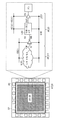
도 1은, 본 발명의 실시 형태 1에 의한 반도체 장치의 구성예를 나타내는 개략도이다. 도 1에는, 반도체 장치는 전체의 레이아웃 구성 예와 그 일부의 영역에 형성되는 회로 예가 도시된다. 도 1에 나타내는 반도체 장치는, 1개의 반도체 칩(CP)으로 구성되며, 특히 한정은 되지 않지만, 대표적으로는, 마이크로 콘트롤러(MCU:Micro Control Unit) 등이다. 반도체 칩(CP)의 외주부에는, 칩 외부와의 결합 단자가 되는 복수의 패드(PD)가 배치된다. 반도체 칩(CP)의 내부에는, 코어 영역(AR_CR)이 설치되고, 코어 영역(AR_CR)과 복수의 패드(PD)의 배치 영역과의 사이에는 IO(Input/Output) 영역(AR_IO)이 마련된다.1 is a schematic diagram showing a configuration example of a semiconductor device according to
코어 영역(AR_CR)에는, 예를 들면, CPU(Central Processing Unit)나, GPIO(General Purpose Input/Output)의 각종 레지스터 등을 대표로 하는 내부 로직 회로(ILOG)가 형성된다. 내부 로직 회로(ILOG)는, 기준 전원 전위(GND)와 그것보다도 고전위인 내부 전원 전위(VDD1)가 공급된다. IO영역(AR_IO)에는, 인버터회로(IV)와 레벨 시프트 회로(LSC)와 드라이버 회로(DV)가 형성된다. 인버터 회로(IV)에는, 기준 전원 전위(GND)와 내부 전원 전위(VDD1)가 공급되며, 레벨 시프트 회로(LSC) 및 드라이버 회로(DV)에는, 기준 전원 전위(GND)와 내부 전원 전위(VDD1)보다도 고전위인 외부 전원 전위(VDD2)가 공급된다.The core region AR_CR is formed with an internal logic circuit ILOG represented by, for example, a CPU (Central Processing Unit) or various registers of GPIO (general purpose input / output). The internal logic circuit ILOG is supplied with the reference power supply potential GND and the internal power supply potential VDD1 which is higher than the reference power supply potential GND. In the IO area AR_IO, an inverter circuit IV, a level shift circuit LSC, and a driver circuit DV are formed. The reference power supply potential GND and the internal power supply potential VDD1 are supplied to the inverter circuit IV and the reference power supply potential GND and the internal power supply potential VDD1 are supplied to the level shift circuit LSC and the driver circuit DV, The external power supply potential VDD2 higher in potential than the power supply potential VDD2 is supplied.
내부 논리 회로(ILOG)는, 소정의 처리를 실행하고, 그 중에서, 레벨 시프트 회로(LSC)의 입력 노드(INT)에, 기준 전원 전위(GND)와 내부 전원 전위(VDD1)와의 사이에서 천이하는 내부 전원 전압 진폭(명세서에서는, VDD1 진폭이라 칭한다)의 입력 신호(INT)를 출력한다. 인버터 회로(IV)는, 레벨 시프트 회로(LSC)의 반전 입력 노드(INT)에, 입력 신호(INT)와 역극성이 되는 반전 입력 신호(INB)를 출력한다.The internal logic circuit ILOG executes a predetermined process and performs a predetermined process on the input node INT of the level shift circuit LSC so as to switch between the reference power supply potential GND and the internal power supply potential VDD1 And outputs the input signal INT of the internal supply voltage amplitude (in the specification, referred to as VDD1 amplitude). The inverter circuit IV outputs an inverted input signal INB which is opposite in polarity to the input signal INT to the inverting input node INT of the level shift circuit LSC.
레벨 시프트 회로(LSC)는, 입력 노드(INT) 또는 반전 입력 노드(INB)의 VDD1 진폭의 입력 신호(INT) 또는 반전 입력 신호(INB)를, 기준 전원 전위(GND)와 외부 전원 전위(VDD2)와의 사이에서 천이하는 외부 전원 전압 진폭(명세서에서는, VDD2 진폭이라 칭한다)의 출력 신호(OUT)로 변환하고, 출력 노드(OUT)로 출력한다. 드라이버 회로(DV)는, 해당 출력 신호(OUT)를, 소정의 구동 능력으로 패드(PD)에 출력한다.The level shift circuit LSC outputs the VDD1 amplitude input signal INT or the inverted input signal INB of the input node INT or the inverted input node INB to the reference power supply potential GND and the external power supply potential VDD2 To an output signal OUT of an external power supply voltage amplitude (referred to as VDD2 amplitude in the specification) that transitions between the output node OUT and the output node OUT. The driver circuit (DV) outputs the output signal (OUT) to the pad (PD) with a predetermined driving capability.
특히 한정은 되지않지만, 대표적으로는, 내부 전원 전위(VDD1)는, 1.2V 등이며, 외부 전원 전위(VDD2)는, 3.3V나 5.0V 등이다. 다만, 내부 전원 전압(VDD1)은, 프로세스의 미세화·저소비 전력화에 따라서, 예를 들면, 1.8V→1.2V→1.0V→…등으로 해마다 저하하고 있다. 한편, 외부 전원 전압(VDD2)은, 미세화와는 관계없이, 예를 들면, GPIO나 I2C(Inter Integrated Circuit) 등이라고 하는 외부 인터페이스의 사양·규격에 기초하여 고정치로 된다.Typically, the internal power source potential VDD1 is 1.2 V or the like and the external power source potential VDD2 is 3.3 V or 5.0 V, for example. However, the internal power supply voltage VDD1 is changed from 1.8V to 1.2V to 1.0V to < RTI ID = 0.0 > And so on. On the other hand, the external power supply voltage VDD2 becomes constant based on specifications and specifications of external interfaces such as GPIO and I2C (Inter Integrated Circuit), for example, regardless of miniaturization.
《레벨 시프트 회로(비교예)의 구성 및 문제점》&Quot; Configuration and problem of level shift circuit (comparative example) "
도 9는, 본 발명의 비교예가 되는 레벨 시프트 회로의 구성 예 및 주요한 동작 예를 나타내는 회로도이다. 도 9에 나타내는 레벨 시프트 회로는, 입력 노드(INT) 및 반전 입력 노드(INB)와 출력 노드(OUT) 및 반전 출력 노드(OUTB)와 한 쌍의 NMOS 트랜지스터(MN0', MN1')와 한 쌍의 PMOS 트랜지스터(MP0', MP1')를 구비한다. 입력 노드(INT) 및 반전 입력 노드(INB)에는, 각각, 입력 신호(INT) 및 그와 역극성이 되는 반전 입력 신호(INB)가 입력되고, 출력 노드(OUT) 및 반전 출력 노드 OUTB는, 각각, 출력 신호(OUT) 및 그와 역극성이 되는 반전 출력신호(OUTB)를 출력한다.9 is a circuit diagram showing a configuration example and a main operation example of a level shift circuit which is a comparative example of the present invention. The level shift circuit shown in Fig. 9 has a pair of NMOS transistors MN0 'and MN1' and a pair of NMOS transistors MN0 'and MN1', an inverting input node INB, an output node OUT and an inverted output node OUTB, And PMOS transistors MP0 'and MP1'. An input signal INT and an inverted input signal INB having a polarity opposite to that of the input signal INT are input to the input node INT and the inverted input node INB, And outputs an output signal OUT and an inverted output signal OUTB which is opposite in polarity to the output signal OUT.
NMOS 트랜지스터(MN0')는, 반전 출력 노드(OUTB)와 기준 전원 전위(GND)와의 사이에 설치되며, 입력 신호(INT)로 구동된다. NMOS 트랜지스터(MN1')는, 출력 노드(OUT)와 기준 전원 전위(GND)와의 사이에 설치되며, 반전 입력 신호(INB)로 구동된다. PMOS 트랜지스터(MP0')는, 외부 전원 전위(VDD2)와 반전 출력 노드(OUTB)와의 사이에 설치되며, 출력 신호(OUT)로 구동된다. PMOS 트랜지스터(MP1')는, 외부 전원 전위(VDD2)와 출력 노드(OUT)와의 사이에 설치되며, 반전 출력 신호(OUTB)로 구동된다.The NMOS transistor MN0 'is provided between the inverted output node OUTB and the reference power supply potential GND, and is driven by the input signal INT. The NMOS transistor MN1 'is provided between the output node OUT and the reference power source potential GND and is driven by the inverted input signal INB. The PMOS transistor MP0 'is provided between the external power supply potential VDD2 and the inverted output node OUTB and is driven by the output signal OUT. The PMOS transistor MP1 'is provided between the external power supply potential VDD2 and the output node OUT and is driven by the inverted output signal OUTB.
도 10은, 명세서에서 사용하는 각 신호의 전위와 각 트랜지스터의 동작 상태를 정의하는 도면이다. 도 10에 나타내듯이, 명세서에서는, 신호의 전위가 기준 전원 전위(GND)인 경우를‘L'로 칭하고, 외부 전원 전위(VDD2)인 경우를‘H'로 칭하고, 내부 전원 전위(VDD1)인 경우를‘Hl'로 칭하고. 또, PMOS 트랜지스터의 스레숄드 전압을 Vtp로서 신호의 전위가“VDD2-Vtp”인 경우를‘Hd'로 칭한다.10 is a diagram for describing the potential of each signal used in the specification and the operation state of each transistor. 10, the case where the potential of the signal is the reference power source potential (GND) is referred to as "L", the case where the external power source potential VDD2 is referred to as "H" The case is referred to as 'Hl'. When the threshold voltage of the PMOS transistor is Vtp and the potential of the signal is " VDD2-Vtp ", this is referred to as " Hd ".
예를 들면, 도 9를 참조해서, 소스에 외부 전원 전위(VDD2)가 인가되는 각 PMOS 트랜지스터는, 게이트에‘Hd'가 인가되는 경우(즉 게이트·소스 간 전압(Vgs라 칭함)이|Vtp|의 경우)에 온과 오프의 경계 상태가 된다. 또, 각 PMOS 트랜지스터는, 게이트에‘Hd'~‘H'가 인가되는 경우에 오프 상태가 되고,‘L'~‘Hd'가 인가되는 경우에 온 상태가 된다. 한편, 소스에 기준 전원 전위(GND)가 인가되는 각 NMOS 트랜지스터는, 스레숄드 전압을 Vtn로 해서 게이트에 Vtn가 인가되는 경우(Vgs=Vtn의 경우)에 온과 오프의 경계 상태가 되고,‘L'~Vtn가 인가되는 경우에 오프 상태가 되고, Vtn~‘H'가 인가되는 경우에 온 상태가 된다.For example, referring to FIG. 9, in each PMOS transistor to which the external power supply potential VDD2 is applied to the source, when `Hd` is applied to the gate (that is, when the gate-source voltage Vgs is | Vtp |), It becomes a boundary state of on and off. In addition, each PMOS transistor is in the off state when 'Hd' to 'H' are applied to the gate and in the on state when 'L' to 'Hd' is applied. On the other hand, each NMOS transistor to which the reference power supply potential (GND) is applied to the source becomes a boundary state between on and off when Vtn is applied to the gate with the threshold voltage as Vtn (Vgs = Vtn) 'To Vtn is applied, and is turned on when Vtn to' H 'are applied.
또, 도 9를 참조해서, 외부 전원 전위(VDD2)와 기준 전원 전위(GND)와의 사이에 직렬로 결합되는 PMOS 트랜지스터(예를 들면 MP0') 및 NMOS 트랜지스터(MN0')가 모두 온이 되는 경우를 가정한다. 이때의 PMOS 트랜지스터의 드레인·소스간 전압(Vds)을 Vdrop(|Vtp|<Vdrop<VDD2)로 해서,“VDD2-Vdrop”를‘Ld'라 칭한다. 즉,‘Ld'의 전위는, PMOS 트랜지스터와 NMOS 트랜지스터의 구동 능력(온 저항)의 비율에 의해 정해지고, 0<Ld<Hd가 된다. 자세한 것은 후술 하지만, VREF는, 0<VREF<Hd의 범위로 설정되는 고정 전위이며,‘X'는,‘L'~‘H'의 범위를 채용할 수 있는 부정 전위이다.9, when both the PMOS transistor (for example, MP0 ') and the NMOS transistor MN0' that are coupled in series between the external power supply potential VDD2 and the reference power supply potential GND are turned on . Vdrop (| Vtp | <Vdrop <VDD2) and "VDD2-Vdrop" are referred to as "Ld" at this time is the drain-source voltage Vds of the PMOS transistor. That is, the potential of 'Ld' is determined by the ratio of the driving capability (on resistance) of the PMOS transistor and the NMOS transistor, and 0 <Ld <Hd. VREF is a fixed potential set in the range of 0 < VREF < Hd, and X is a negative potential capable of employing a range of L to H.
도 9의 위의 도면에는, 입력 노드(INT)가‘Hl', 반전 입력 노드(INB)가‘L'이다 경우의 정상 시의 회로 상태가 도시된다. 이 경우, NMOS 트랜지스터(MN0') 및 PMOS 트랜지스터(MP1')가 온이며, NMOS 트랜지스터(MN1') 및 PMOS트랜지스터(MP0')가 오프이다. 그리고, 출력 노드(OUT)는‘H'가 되고, 반전 출력 노드(OUTB)는‘L'가 된다.9 shows a circuit state at the normal time when the input node INT is 'Hl' and the inverting input node INB is 'L'. In this case, the NMOS transistor MN0 'and the PMOS transistor MP1' are on, and the NMOS transistor MN1 'and the PMOS transistor MP0' are off. Then, the output node OUT becomes 'H' and the inverted output node OUTB becomes 'L'.
이 상태를 기점으로서 도 9의 아래 도면에는, 입력 노드(INT)가‘Hl'로부터‘L'로 천이(반전 입력 노드(INB)가‘L'로부터‘Hl'로 천이) 하는 경우의 회로 상태가 도시된다. NMOS 트랜지스터(MN1')는, 반전 입력 노드(INB)의 천이에 대응해서 오프로부터 온으로 천이하고, NMOS 트랜지스터(MN0')는, 입력 노드(INT)의 천이에 대응해서 온으로부터 오프로 천이한다.9 shows the circuit state when the input node INT transits from 'H1' to 'L' (the transition of the inverted input node INB changes from 'L' to 'H1'), Lt; / RTI > The NMOS transistor MN1 'transitions from off to on in response to the transition of the inverting input node INB and the NMOS transistor MN0' transitions from on to off in response to the transition of the input node INT .
이것에 의해, 이상적으로는, NMOS 트랜지스터(MN1')는, 출력 노드(OUT)를‘H'로부터‘Hd'보다 작은 전위로 천이시키고, 이것에 의해 PMOS 트랜지스터(MP0')를 오프로부터 온으로 천이시킨다. PMOS 트랜지스터(MP0')가 온으로 천이하면, 반전출력 노드(OUTB)는,‘H'를 향해서 천이하고, PMOS 트랜지스터(MP1')는 오프를 향해서 천이한다. NMOS 트랜지스터(MN1')는, 이 PMOS 트랜지스터(MP1')의 천이에 수반해서, 출력 노드(OUT)를 용이하게‘L'로 천이시킬 수 있다.Thus, ideally, the NMOS transistor MN1 'shifts the output node OUT from the H level to a potential lower than Hd, thereby turning the PMOS transistor MP0' from off to on Transit. When the PMOS transistor MP0 'transitions to ON, the inverted output node OUTB transitions toward' H 'and the PMOS transistor MP1' transitions to OFF. The NMOS transistor MN1 'can easily transition the output node OUT to' L 'with the transition of the PMOS transistor MP1'.
그러나, 실제로는, NMOS 트랜지스터(MN1')가, 출력 노드(OUT)를‘H'로부터‘Hd'보다도 작은 전위로 천이시키려고 할 때에, PMOS 트랜지스터(MP1')의 게이트에는, 플로팅 상태의 반전 출력 노드(OUTB)에 의해‘L'가 인가되어 있다. 이것에 의해, PMOS 트랜지스터(MP1')는, Vgs가 VDD2 레벨이기 때문에 큰 드레인·소스간 전류(이후, Ids라 칭한다)를 흐르게 하는 상태로 온이 되어있다.Actually, however, when the NMOS transistor MN1 'attempts to transition the output node OUT from the H level to a potential lower than Hd, the gate of the PMOS transistor MP1' &Quot; L " is applied by the node OUTB. Thus, the PMOS transistor MP1 'is turned on in a state where a large drain-source current (hereinafter referred to as Ids) flows because Vgs is at VDD2 level.
여기서, 만일, NMOS 트랜지스터(MN1')가 흘릴 수 있는 Ids가 PMOS 트랜지스터(MP1')를 흘릴 수 있는 Ids보다도 작은 경우, NMOS 트랜지스터(MN1')는, 출력 노드(OUT)를‘Hd'보다 작은 전위로 천이시키는 것이 곤란해질 수 있다. 여기서, 트랜지스터의 Ids는, Vgs에 의존한다. NMOS 트랜지스터(MN1')의 Vgs가 VDD1레벨인데 대해, PMOS 트랜지스터(MP1')의 Vgs는 VDD2 레벨이다. 그 결과, 외부 전원 전위(VDD2)와 내부 전원 전위(VDD1)와의 전위차가 확대함(예를 들면, VDD1가 상대적으로 저하한다)에 따라, 출력 노드(OUT)가 천이하기 어렵게 되고, 결과적으로, 레벨 시프트 동작을 실시할 수 있는 전원 전위 범위가 한정될 우려가 있다.Here, if the Ids that the NMOS transistor MN1 'can flow through is smaller than the Ids that can flow through the PMOS transistor MP1', the NMOS transistor MN1 'has the output node OUT smaller than' Hd ' It may be difficult to shift the potential to the potential. Here, the transistor Ids depends on Vgs. Vgs of the NMOS transistor MN1 'is at the VDD1 level whereas Vgs of the PMOS transistor MP1' is at the VDD2 level. As a result, as the potential difference between the external power supply potential VDD2 and the internal power supply potential VDD1 increases (for example, VDD1 relatively decreases), the output node OUT becomes difficult to transition, and as a result, There is a possibility that the power supply potential range capable of performing the level shift operation is limited.
도 11은, 도 9의 레벨 시프트 회로에 있어서의 문제점의 일례를 보다 구체적으로 설명하는 도면이다. 도 9에서 정상적인 레벨 시프트 동작을 실현하기 위한 방법으로서 NMOS 트랜지스터(예를 들면 MN1')의 구동 능력(바꾸어 말하면 트랜지스터 사이즈)을 PMOS 트랜지스터(MP1')의 구동 능력보다 충분히 높게 하는 방법을 들 수 있다. 도 11은, VD D2=5.0 V, PMOS 트랜지스터(MP0', MP1')의 스레숄드치 전압을 1.0 V로 했을 경우에서, 정상적인 레벨 시프트 동작(정상적인 출력 신호(OUT)의 천이)를 실현하기 위해 필요한 PMOS 트랜지스터(MP1')에 대한 NMOS 트랜지스터(MN1')의 사이즈 비의 일례를 나타내는 도면이다.11 is a diagram for more specifically explaining an example of a problem in the level shift circuit of Fig. As a method for realizing a normal level shift operation in FIG. 9, there is a method of making the driving capability (in other words, the transistor size) of the NMOS transistor MN1 '(for example, the transistor size) sufficiently higher than the driving capability of the PMOS transistor MP1' . 11 is a graph showing the relationship between the threshold voltage of VDD2 = 5.0 V and the threshold voltage of the PMOS transistors MP0 'and MP1' set at 1.0 V, which is necessary for realizing a normal level shift operation (transition of the normal output signal OUT) Is a diagram showing an example of the size ratio of the NMOS transistor MN1 'to the PMOS transistor MP1'.
예를 들면, 내부 전원 전압(VDD1(=NMOS 트랜지스터(MN1')의 Vgs)이 1.5V의 경우, PMOS 트랜지스터(MP1')에 대해서 NMOS 트랜지스터(MN1')를 2.5배 이상의 사이즈로 정하면, 정상적인 레벨 시프트 동작을 실현할 수 있다. 한편, 내부 전원전압(VDD1)이 1.0 V에서는, NMOS 트랜지스터(MN1')를 13배 이상의 사이즈로 정할 필요가 있으며, 0.9 V, 0.8 V에서는, 각각, 24배 이상, 63배 이상으로 정할 필요가 있다. 그 결과, 외부 전원 전위(VDD2)와 내부 전원 전위(VDD1)와의 전위차가 확대하는 만큼, 회로 면적의 증대가 생길 수 있다.For example, when the internal power supply voltage VDD1 (= Vgs of the NMOS transistor MN1 ') is 1.5V, if the size of the NMOS transistor MN1' is set to 2.5 times or more the size of the PMOS transistor MP1 ' When the internal supply voltage VDD1 is 1.0 V, it is necessary to set the size of the NMOS transistor MN1 'to 13 times or more, and when the internal supply voltage VDD1 is 0.9 V and 0.8 V, It is necessary to set it to 63 times or more. As a result, as the potential difference between the external power supply potential VDD2 and the internal power supply potential VDD1 increases, the circuit area may increase.
더욱이, 회로 면적의 증대가 생기면, 동작 속도에도 영향을 미친다. 예를 들면 도 9에 있어서, 출력 노드(OUT)에 보이는 용량 중 PMOS 트랜지스터(MP1') 및 NMOS트랜지스터(MN1')의 확산 용량(드레인 용량)에 주목한다. 내부 전원 전압(VDD1)이 1.5V의 경우의 확산 용량은, PMOS 트랜지스터(MP1')와 NMOS 트랜지스터(MN1')의 사이즈를 합계해서 3.5(=1+2. 5)가 되고, 내부 전원 전압(VDD1)이 1.0V의 경우의 확산 용량은, 마찬가지로 해서 14(=1+13)가 된다. 그 결과, 내부 전원 전압(VDD1)이 1.0 V의 경우의 확산 용량은, 내부 전원 전압(VDD1)이 1.5V의 경우에 비해서 4배가 된다.Furthermore, if an increase in the circuit area occurs, the operation speed is also affected. For example, in FIG. 9, the diffusion capacities (drain capacitances) of the PMOS transistor MP1 'and the NMOS transistor MN1' among the capacitors shown in the output node OUT are noted. The diffusion capacity when the internal power supply voltage VDD1 is 1.5 V is 3.5 (= 1 + 2.5) by summing the sizes of the PMOS transistor MP1 'and the NMOS transistor MN1' The diffusion capacity in the case of 1.0 V is 14 (= 1 + 13) in the same manner. As a result, the diffusion capacity when the internal supply voltage VDD1 is 1.0 V is quadrupled as compared with the case where the internal supply voltage VDD1 is 1.5V.
이와 같이 용량이 증가하면, 출력 신호(OUT)의 천이시의 충 방전에 필요로 하는 시간이 증대하고, 동작 속도가 저하할 우려가 있다. 또, 동작 속도의 향상을 도모하는 방법으로서 구동전류를 증가시키는 것을 생각할 수 있지만, 이 방법이 제약될 우려도 있다. 구체적으로는, 예를 들면, 구동 전류를 늘리기 위해서, PMOS 트랜지스터(MP1')의 트랜지스터 사이즈를 크게 하는 경우를 상정한다. 이 경우, 전술한 것처럼, 외부 전원 전위(VDD2)와 내부 전원 전위(VDD1)와의 전위차가 확대함에 따라, 보다 큰 출력 용량이 NMOS 트랜지스터(MN1')에 의해 부가되어 버려, 동작 속도의 향상을 저해한다. 이 때문에, 구동 전류에 의해서 동작 속도의 향상을 도모하기 위해서는, 외부 전원 전위(VDD2)와 내부 전원 전위(VDD1)와의 전위차가 어느 정도 작은 것이 필요할 수 있다.If the capacity increases as described above, the time required for charging and discharging at the time of transition of the output signal OUT increases, and the operation speed may decrease. In addition, although it is conceivable to increase the driving current as a method of improving the operating speed, there is a possibility that this method is restricted. Specifically, it is assumed that the transistor size of the PMOS transistor MP1 'is increased in order to increase the driving current, for example. In this case, as described above, as the potential difference between the external power supply potential VDD2 and the internal power supply potential VDD1 increases, a larger output capacitance is added by the NMOS transistor MN1 ' do. Therefore, in order to improve the operating speed by the driving current, it is necessary that the potential difference between the external power supply potential VDD2 and the internal power supply potential VDD1 be small to some extent.
이상과 같이, 도 9의 레벨 시프트 회로에서는, 외부 전원 전위(VDD2)와 내부 전원 전위(VDD1)와의 전위차가 확대함(예를 들면, VDD1가 상대적으로 저하한다)에 따라서, 소정의 성능을 만족하면서 레벨 시프트 동작을 실시하는 것이 곤란해질 수 있다. 구체적으로는, 예를 들면, 회로 면적의 저감이나 동작 속도의 향상을 도모하면서, 레벨 시프트 동작을 실시하는 것이 곤란해질 수 있다. 그 결과, 실 사용상의 관점에서, 레벨 시프트 동작을 실시할 수 있는 전원 전위 범위가 작게 될 우려가 있다.As described above, in the level shift circuit of Fig. 9, when the potential difference between the external power supply potential VDD2 and the internal power supply potential VDD1 increases (for example, VDD1 relatively decreases), predetermined performance is satisfied It may be difficult to perform the level shift operation. Concretely, for example, it may become difficult to perform the level shift operation while reducing the circuit area and improving the operation speed. As a result, from the viewpoint of practical use, there is a fear that the power supply potential range capable of performing the level shift operation becomes small.
《레벨 시프트 회로(실시 형태 1)의 구성》&Quot; Configuration of level shift circuit (first embodiment) "
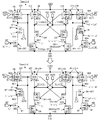
도 2a는, 본 발명의 실시 형태 1에 의한 레벨 시프트 회로의 구성예를 나타내는 회로도이다. 도 2a에 나타내는 레벨 시프트 회로는, 도 9의 경우와 같은 입력 노드(INT), 반전 입력 노드(INB), 출력 노드(OUT) 및 반전 출력 노드(OUTB)에 더해서, 진폭 증폭 회로(AMPt1, AMPb1)와 서브 레벨 시프트 회로(SLSC1)를 구비하고 있다. 진폭 증폭 회로(AMPt1, AMPb1) 및 서브 레벨 시프트 회로(SLSC1)에는, 모두, 기준 전원 전위(GND) 및 외부 전원 전위(VDD2)가 공급된다.2A is a circuit diagram showing a configuration example of a level shift circuit according to
진폭 증폭 회로(AMPt1, AMPb1)는, 입력 노드(INT) 및 반전 입력 노드(INB)로부터의 VDD1 진폭의 입력 신호(INT) 및 반전 입력 신호(INB)를 받아서, 노드(ND1, ND2)에, VDD1 진폭보다 크고 VDD2 진폭보다 작은 전압 진폭의 신호(SND1, SND2)를 각각 출력한다. 서브 레벨 시프트 회로(SLSC1)는, 진폭증폭 회로(AMPt1, AMPb1)로부터의 신호(SND1, SND2)를 받아서, 출력 노드(OUT) 및 반전 출력 노드(OUTB)에, VDD2 진폭의 출력 신호(OUT) 및 반전 출력 신호(OUTB)를 출력한다.The amplitude amplifying circuits AMPt1 and AMPb1 receive the input signal INT and the inverted input signal INB of VDD1 amplitude from the input node INT and the inverted input node INB and output the inverted input signal INT to the nodes ND1 and ND2, (SND1, SND2) having a voltage amplitude larger than the VDD1 amplitude and smaller than the VDD2 amplitude, respectively. The sub level shift circuit SLSC1 receives the signals SND1 and SND2 from the amplitude amplification circuits AMPt1 and AMPb1 and outputs the output signal OUT having the amplitude of VDD2 to the output node OUT and the inverted output node OUTB. And an inverted output signal OUTB.
구체적으로는, 진폭 증폭 회로(AMPt1)는, NMOS 트랜지스터(MN0)와 부하 회로(LDt1)를 가진다. NMOS 트랜지스터(MN0)는, 노드(ND1)와 기준 전원 전위 (GND)와의 사이에 드레인·소스 경로가 설치되며, 입력 신호(INT)에 의해 게이트가 구동된다. 부하 회로(LDt1)는, 외부 전원 전위(VDD2)와 노드(ND1)와의 사이에 설치되어 NMOS 트랜지스터(MN0)에 흐르는 전류에 대응한 신호(SND1)를 노드(ND1)에 출력한다. 부하 회로(LDt1)는, 여기에서는, 외부 전원 전위(VDD2)와 노드(ND1)와의 사이에 소스·드레인 경로가 설치되며, 노드(ND1)의 신호(SND1)에 의해 게이트가 구동되는 PMOS 트랜지스터(MP0)에 의해 구성된다.Specifically, the amplitude amplifying circuit AMPt1 has an NMOS transistor MN0 and a load circuit LDt1. In the NMOS transistor MN0, a drain-source path is provided between the node ND1 and the reference power-supply potential GND, and the gate is driven by the input signal INT. The load circuit LDt1 outputs a signal SND1 provided between the external power supply potential VDD2 and the node ND1 and corresponding to the current flowing through the NMOS transistor MN0 to the node ND1. The load circuit LDt1 is a PMOS transistor in which a source and a drain path are provided between the external power supply potential VDD2 and the node ND1 and a gate is driven by the signal SND1 of the node ND1 MP0.
마찬가지로, 진폭 증폭 회로(AMPb1)는, NMOS 트랜지스터(MN3)와 부하 회로(LDb1)를 가진다. NMOS 트랜지스터(MN3)는, 노드(ND2)와 기준 전원 전위(GND)와의 사이에 드레인·소스 경로가 설치되고, 반전 입력 신호(INB)에 의해 게이트가 구동한다. 부하 회로(LDb1)는, 외부 전원 전위(VDD2)와 노드(ND2)와의 사이에 설치되어 NMOS 트랜지스터(MN3)에 흐르는 전류에 대응한 신호(SND2)를 노드(ND2)에 출력한다. 부하 회로(LDb1)는, 여기에서는, 외부 전원 전위(VDD2)와 노드(ND2)와의 사이에 소스·드레인 경로가 설치되며, 노드(ND2)의 신호(SND2)에 의해 게이트가 구동되는 PMOS 트랜지스터(MP3)에 의해 구성된다.Similarly, the amplitude amplifying circuit AMPb1 has an NMOS transistor MN3 and a load circuit LDb1. In the NMOS transistor MN3, a drain-source path is provided between the node ND2 and the reference power-supply potential GND, and the gate is driven by the inverting input signal INB. The load circuit LDb1 outputs a signal SND2 that is provided between the external power supply potential VDD2 and the node ND2 and corresponds to the current flowing through the NMOS transistor MN3 to the node ND2. The load circuit LDb1 is a PMOS transistor in which a source and a drain path are provided between the external power supply potential VDD2 and the node ND2 and a gate is driven by the signal SND2 of the node ND2 MP3).
서브 레벨 시프트 회로(SLSC1), 한 쌍의 NMOS 트랜지스터(N1, MN2)와 한 쌍의 PMOS 트랜지스터(MP1, MP2)를 가진다. NMOS 트랜지스터(MN1)는, 출력 노드(OUT)와 기준 전원 전위(GND)와의 사이에 드레인·소스 경로가 설치되며, 반전 출력 신호(OUTB)에 의해 게이트가 구동된다. NMOS 트랜지스터(MN2)는, 반전 출력 노드(OUTB)와 기준 전원 전위(GND)와의 사이에 드레인·소스 경로가 설치되고, 출력 신호(OUT)에 의해 게이트가 구동된다.A sub level shift circuit SLSC1, a pair of NMOS transistors N1 and MN2 and a pair of PMOS transistors MP1 and MP2. In the NMOS transistor MN1, a drain-source path is provided between the output node OUT and the reference power-supply potential GND, and the gate is driven by the inverted output signal OUTB. In the NMOS transistor MN2, a drain-source path is provided between the inverted output node OUTB and the reference power-supply potential GND, and the gate is driven by the output signal OUT.
PMOS 트랜지스터(MP1)는, 외부 전원 전위(VDD2)와 출력 노드(OUT)와의 사이에 소스·드레인 경로가 설치되며, 노드(ND1)의 신호(SND1)에 의해 게이트가 구동되고. PMOS 트랜지스터(MP2)는, 외부 전원 전위(VDD2)와 반전 출력 노드(OUTB)와의 사이에 소스·드레인 경로가 설치되고, 노드(ND2)의 신호(SND2)에 의해 게이트가 구동된다.A source-drain path is provided between the external power supply potential VDD2 and the output node OUT and the gate of the PMOS transistor MP1 is driven by the signal SND1 of the node ND1. The PMOS transistor MP2 is provided with a source-drain path between the external power supply potential VDD2 and the inverted output node OUTB and the gate thereof is driven by the signal SND2 of the node ND2.
여기서, 서브 레벨 시프트 회로(SLSC1)는, 도 9의 회로에 비해서, 한 쌍의 NMOS 트랜지스터와 한 쌍의 PMOS 트랜지스터를 바꿔 넣은 것 같은 구성을 구비한다. 그 결과, 도 9의 회로가 기준 전원 전위(GND)를 기준으로서 신호의 전압 진폭을 변환하는데 대해서, 서브 레벨 시프트 회로(SLSC1)는, 외부 전원 전위(VDD2)를 기준으로서 신호의 전압 진폭을 변환하게 된다. 이러한 차이를 제외하고, 양자의 기본적인 동작은 거의 같다. The sublevel shift circuit SLSC1 has a configuration in which a pair of NMOS transistors and a pair of PMOS transistors are switched as compared with the circuit of Fig. As a result, while the circuit of Fig. 9 converts the voltage amplitude of the signal with reference to the reference power source potential GND, the sub level shift circuit SLSC1 converts the voltage amplitude of the signal based on the external power source potential VDD2 . Except for these differences, the basic behavior of both is almost the same.
다만, 큰 차이점으로서 서브 레벨 시프트 회로(SLSC1)는, 도 9의 회로와 달리, 진폭 증폭 회로(AMPt1, AMPb1)로부터의 VDD1 진폭보다 크고 VDD2 진폭보다 작은 전압 진폭의 신호(SND1, SND2)를 받아 레벨 시프트 동작을 실시하는 점을 들 수 있다. 또, 진폭 증폭 회로(AMPt1, AMPb1)의 특징으로서 PMOS 트랜지스터(MP0, MP3)는, VDD2 진폭보다 작은 전압 진폭으로 온으로 구동되는 점을 들 수 있다.However, unlike the circuit of Fig. 9, the sub level shift circuit SLSC1 receives signals SND1 and SND2 having a voltage amplitude larger than the VDD1 amplitude and smaller than the VDD2 amplitude from the amplitude amplification circuits AMPt1 and AMPb1 And a level shift operation is performed. The characteristic of the amplitude amplifying circuits AMPt1 and AMPb1 is that the PMOS transistors MP0 and MP3 are driven on at a voltage amplitude smaller than the VDD2 amplitude.
《레벨 시프트 회로(실시 형태 1)의 동작》&Quot; Operation of level shift circuit (first embodiment) "
도 2B는, 도 2a에 있어서의 정상 상태에서의 각 노드 및 각 트랜지스터 상태예를 나타내는 회로도이며, 도 2c는, 도 2a에 있어서의 천이 기간에서의 각 노드 및 각 트랜지스터의 상태 천이의 일례를 나타내는 회로도이다. 도 2d는, 도 2a에 있어서, 입력 신호의 천이에 따르는 각 노드 및 각 트랜지스터의 시계열적인 상태 천이의 일례를 요약한 천이도이며, 도 2e는, 도 2d와는 역방향의 입력 신호의 천이에 따르는 각 노드 및 각 트랜지스터의 시계열적인 상태 천이의 일례를 요약한 천이도이다.Fig. 2B is a circuit diagram showing an example of each node and each transistor state in the steady state in Fig. 2A, and Fig. 2C is a diagram showing an example of state transition of each node and each transistor in the transition period in Fig. 2A Circuit diagram. FIG. 2 (d) is a transition diagram summarizing an example of a time-series state transition of each node and each transistor in response to a transition of an input signal in FIG. 2a. FIG. 2 Is a transition diagram summarizing an example of a time-series state transition of a node and each transistor.
도 2d의 천이도에 나타내는 각 기간(Time)은, 상태 천이의 관점에서 편의적으로 구획되어 있으며, 같은 길이로는 한정되지 않는다. 또, 해당 천이도에서 이용하는 각 전위의 의미는, 도 10에 나타낸 바와 같다. 덧붙여, 해당 천이도에서는, 노드의 전위가 인상하고 있는 상태를“X↑”그리고 나타내고, 인하하고 있는 상태를“X↓”로 나타내고 있다. 또, 트랜지스터 상태인“[OFF]”는, 완전한“OFF”는 아니고, 온과 오프의 경계 상태인 것을 나타낸다. 이러한 사항은, 도 2e의 천이도나, 이후의 실시 형태에서 이용하는 각 천이도에 있어서도 같다.Each period (Time) shown in the transition diagram of Fig. 2D is delimited conveniently from the viewpoint of state transition, and is not limited to the same length. The meanings of the potentials used in the transition diagram are as shown in Fig. In addition, in the transition diagram, the state in which the potential of the node is pulled up is indicated by "X ↑", and the state in which the potential is lowered is indicated by "X ↓". In addition, the transistor state "[OFF]" indicates not the complete "OFF" but a boundary state between on and off. The same applies to the transition shown in Fig. 2E and the transition diagram used in the subsequent embodiments.
우선, 입력 노드(INT)가‘Hl'(=VDD1)로부터‘L'로 천이하고, 이것에 대응해서, 출력 노드(OUT)가‘H'(=VDD2)로부터‘L'로 천이하는 경우에 대해 설명한다. 도 2d의 초기 기간(Time=0)(바꾸어 말하면, 정상 상태)에서는, 각 노드 및 각 트랜지스터는, 도 2b에 나타나는 것과 같은 상태가 되고 있다. 도 2d의“Time=0”및 도 2b에 있어서, 입력 노드(INT)는‘Hl'이며, 반전 입력 노드(INB)는‘L'이다. 이것에 대응해서 NMOS 트랜지스터(MN0)는 온이며, NMOS 트랜지스터(MN3)는 오프이다.First, when the input node INT transitions from 'Hl' (= VDD1) to 'L' and the output node OUT transits from 'H' (= VDD2) to 'L' . In the initial period (Time = 0) (in other words, the normal state) of FIG. 2D, each node and each transistor is in a state as shown in FIG. 2B. In Fig. 2D, "Time = 0" and in Fig. 2B, the input node INT is 'Hl' and the inverting input node INB is 'L'. In response to this, the NMOS transistor MN0 is turned on and the NMOS transistor MN3 is turned off.
노드(ND1)는, NMOS 트랜지스터(MN0)의 온에 따라‘Ld'(=VDD2-Vdrop)이다. Vdrop는, 도 10에서 말한 것처럼, 모두 온 상태가 되는 PMOS 트랜지스터(MP0) 및 NMOS 트랜지스터(MN0)의 Ids가 균형되는 경우에, PMOS 트랜지스터 (MP0)에 인가되는 드레인·소스간 전압 Vds(=Vgs)이다. PMOS 트랜지스터(MP1)는, 노드(ND)의‘Ld'에 따라 온이다.The node ND1 is 'Ld' (= VDD2-Vdrop) according to the turn-on of the NMOS transistor MN0. Vdrop is a drain-source voltage Vds (= Vgs) applied to the PMOS transistor MP0 when the Ids of the PMOS transistor MP0 and the NMOS transistor MN0 that are all turned on are balanced, )to be. The PMOS transistor MP1 is turned on in accordance with 'Ld' of the node ND.
노드(ND2)는, NMOS 트랜지스터(MN3)의 오프에 따라‘Hd'(=VDD2-|Vtp|)이다. 이것에 따라, PMOS 트랜지스터(MP3, MP2)는, 온과 오프의 경계 상태가 된다. 출력 노드(OUT)는,‘H'이며, 반전 출력 노드(OUTB)는‘L'이다. 이것에 따라서, NMOS 트랜지스터(MN2)는, 온이며, NMOS 트랜지스터(MN1)는, 오프이다.The node ND2 is 'Hd' (= VDD2- | Vtp |) when the NMOS transistor MN3 is turned off. Thus, the PMOS transistors MP3 and MP2 are in a boundary state between on and off. The output node OUT is 'H', and the inverted output node OUTB is 'L'. Accordingly, the NMOS transistor MN2 is turned on and the NMOS transistor MN1 is turned off.
다음에, 도 2d의“Time=1~4”에 대해서 설명한다. 이“Time=1~4”에 거의 대응하는 기간에서의 상태 천이는, 도 2c에 나타난다. 도 2d의“Time=1”에서 입력 노드(INT)가‘Hl'로부터‘L'로 천이하면, “Time=2”에서 NMOS 트랜지스터(MN0)는 온으로부터 오프로 천이한다. 노드(ND1)는, NMOS 트랜지스터(MN0)가 오프로 천이함으로써,“Time=3”이후‘Ld'로부터‘Hd'로 천이한다. 이것에 대응해서 PMOS 트랜지스터(MP0, MP1)는, 온으로부터 경계 상태로 천이한다.Next, "Time = 1 to 4" in FIG. 2D will be described. The state transition in a period substantially corresponding to " Time = 1 to 4 " is shown in Fig. 2C. When the input node INT transitions from 'H1' to 'L' in FIG. 2D 'Time = 1', the NMOS transistor MN0 transitions from on to off at Time = 2. The node ND1 transits from 'Ld' to 'Hd' after "Time = 3" by turning off the NMOS transistor MN0. In response to this, the PMOS transistors MP0 and MP1 transition from the ON state to the boundary state.
한편, 도 2d의“Time=1”에서 반전 입력 노드(INB)가‘L'로부터‘Hl'로 천이하면“Time=2”에서 NMOS 트랜지스터(MN3)는 오프로부터 온으로 천이한다. 이 천이의 시점에서, 노드(ND2)는‘Hd'이며, PMOS 트랜지스터(MP3)의 Vgs는 Vtp이다. Vgs=Vtp에서는, PMOS 트랜지스터(MP3)의 Ids는, 이상적으로는 0이다. 따라서,“Time=3”이후, NMOS 트랜지스터(MN3)는, Vgs=Hl'(=VDD1)에 따라 Ids가 작은 상태에서도, 노드(ND2)의 전위를 용이하게 인하할 수 있다.On the other hand, when the inverted input node INB transits from 'L' to 'Hl' in FIG. 2D 'Time = 1', the NMOS transistor MN3 transitions from off to on at Time = 2. At the time of this transition, the node ND2 is 'Hd', and the Vgs of the PMOS transistor MP3 is Vtp. At Vgs = Vtp, the Ids of the PMOS transistor MP3 is ideally zero. Therefore, after "Time = 3", the NMOS transistor MN3 can easily lower the potential of the node ND2 even when Ids is small according to Vgs = Hl '(= VDD1).
즉, PMOS 트랜지스터(MP3)는, 도 9의 경우와 같이 VDD2 진폭에서 온으로 구동되는 트랜지스터가 아니라, VDD2 진폭보다 작은 전압 진폭에서 온으로 구동되는 트랜지스터이다. 그 결과, NMOS 트랜지스터(MN3)는, 해당 PMOS 트랜지스터(MP3)의 드레인 전위(노드 ND2의 전위)를, 도 9의 경우보다 용이하게 인하시킬 수 있다.That is, the PMOS transistor MP3 is not a transistor driven ON at the VDD2 amplitude but a transistor driven ON at a voltage amplitude smaller than the VDD2 amplitude as in the case of FIG. As a result, the NMOS transistor MN3 can lower the drain potential (potential of the node ND2) of the PMOS transistor MP3 more easily than in the case of FIG.
노드(ND2)의 전위가 인하하면, PMOS 트랜지스터(MP3, MP2)는 모두 경계상태로부터 온으로 천이하고, 노드(ND2)는,‘Ld'가 된다. 또, PMOS 트랜지스터(MP2)가 온으로 천이함으로써, 반전 출력 노드(OUTB)는‘L'로부터 인상된다. 다만, 이 시점에서는, 도 2c에 나타내듯이, 출력 노드(OUT)의‘H'(=VDD2)에 따라 NMOS 트랜지스터(MN2)도 온이기 때문에, 도 9의 경우와 같은 이유로써, 반전 출력 노드(OUTB)의 인상 능력이 문제가 될 수 있다.When the potential of the node ND2 is lowered, the PMOS transistors MP3 and MP2 all transition from the boundary state to the on state, and the node ND2 becomes 'Ld'. In addition, the PMOS transistor MP2 transitions to the ON state, and the inverted output node OUTB is pulled up from "L". At this point, however, the NMOS transistor MN2 is turned on in accordance with the H (= VDD2) of the output node OUT as shown in Fig. 2C, OUTB) can be a problem.
여기서, 도 9의 경우에는, VDD2 진폭에서 온으로 구동되고 있는 PMOS 트랜지스터(MP1')의 드레인 전위를, VDD1 진폭에서 온으로 구동되는 NMOS 트랜지스터(MN1')에서 인하하고 있다. 한편, 도 2c의 경우에는, VDD2 진폭에서 온으로 구동되고 있는 NMOS 트랜지스터(MN2)의 드레인 전위를,|Vdrop|진폭에서 온으로 구동되는 PMOS 트랜지스터(MP2)에서 인상하고 있다. 이때에, 진폭 증폭 회로(AMPb1)는, VDD1 진폭의 반전 입력 신호(INB)를, VDD1 진폭보다 크고 VDD2 진폭보다도 작은|Vdrop|진폭의 신호(SND2)로 증폭한 다음 서브 레벨 시프트 회로(SLSC1)로 출력하는 역할을 담당한다. 이와 같이 해서, 서브 레벨 시프트 회로(SLSC1)의 입력 전압 진폭을 VDD1 진폭이 아니라|Vdrop|진폭으로 함으로써, 반전 출력 노드(OUTB)의 인상 능력을 충분히 확보하는 것이 가능하게 된다.Here, in the case of FIG. 9, the drain potential of the PMOS transistor MP1 'which is driven on with the amplitude of VDD2 is lowered by the NMOS transistor MN1' driven on by the amplitude of VDD1. On the other hand, in the case of FIG. 2C, the drain potential of the NMOS transistor MN2 which is driven to be ON at the VDD2 amplitude is pulled up by the PMOS transistor MP2 driven on at the amplitude of | Vdrop |. At this time, the amplitude amplifying circuit AMPb1 amplifies the inverted input signal INB having the amplitude of VDD1 to a signal SND2 having a magnitude larger than the amplitude VDD1 and smaller than the amplitude VDD2 with the amplitude | Vdrop | As shown in FIG. In this manner, by making the input voltage amplitude of the sublevel shift circuit SLSC1 equal to | Vdrop | amplitude rather than VDD1 amplitude, it is possible to sufficiently secure the pull-up capability of the inverted output node OUTB.
도 2d의“Time=5”에서 반전 출력 노드(OUTB)가‘L'로부터 Vtn 이상으로 인상하면“Time=6”에서 NMOS 트랜지스터(MN1)가 오프로부터 온으로 천이하고, 출력노드(OUT)는,‘H'로부터 인하한다. 출력 노드(OUT)가 Vtn 미만으로 인하하면,“Time=7”에서 NMOS 트랜지스터 MN2는, 온으로부터 오프로 천이하고, 이것에 따라 반전 출력 노드(OUTB)는‘H'로 수속한다. 또,“Time=8”에서는, 온 상태의 NMOS 트랜지스터(MN1)를 거쳐서 출력 노드(OUT)는‘L'로 수속하고, Time=9”에서, 입력 신호(INT)가‘L'시의 정상 상태가 된다.The NMOS transistor MN1 transitions from off to on at Time = 6 and the output node OUT transitions from off to on when the inverted output node OUTB rises from L to Vtn at Time = , &Quot; H ". When the output node OUT is lowered below Vtn, the NMOS transistor MN2 transitions from ON to OFF at "Time = 7", and the inverted output node OUTB is set to "H" accordingly. At Time = 8, the output node OUT converges to the L level via the on-state NMOS transistor MN1. At Time = 9, the input signal INT is at the normal State.
입력 신호 INT가‘L'시의 정상 상태에서는, 도 2b에 있어서, 대칭 관계가 되는 한쪽 편의 상태와 또 다른 한쪽 편의 상태를 바꿔 넣은 것 같은 상태가 된다. 구체적으로는, INT, OUT,ND1, MN0, MN1, MP0, MP1와 INB, OUTB, ND2, MN3, MN2, MP3, MP2를 각각 바꿔 넣은 것 같은 상태가 된다. 또, 도 2e의“Time=10~19”에는, 도 2d의“Time=0~9”와는 반대로, 입력 노드 INT가‘L'로부터‘Hl'로 천이하는 경우의 천이 상태가 나타난다. 도 2e의 천이 상태도, 도 2d의 천이 상태에 대해서, 대칭 관계가 되는 한쪽 편 상태와 또 다른 한쪽 편 상태를 바꿔 넣은 것 같은 상태가 된다.In the normal state when the input signal INT is at "L", a state in which the state of one side of the symmetrical relationship and the state of the other side of the symmetrical relationship are switched is shown in FIG. 2B. Concretely, it is as if the INT, OUT, ND1, MN0, MN1, MP0, MP1 and INB, OUTB, ND2, MN3, MN2, MP3, 2E, a transition state occurs when the input node INT transits from 'L' to 'Hl', as opposed to 'Time = 0 to 9' in FIG. 2D. The transition state of Fig. 2E also becomes a state where the one side state and the other side state which are symmetrical with respect to the transition state of Fig. 2D are switched.
즉, 예를 들면, 도 2e의 입력 노드(INT) 상태는, 도 2d의 반전 입력 노드(INB) 상태가 되고, 도 2e의 반전 입력 노드(INB) 상태는, 도 2d의 입력 노드(INT)의 상태가 된다. 또, 도 2e의 NMOS 트랜지스터(MN0) 상태는, 도 2d의NMOS 트랜지스터(MN3) 상태가 되며, 도 2e의 NMOS 트랜지스터(MN3) 상태는, 도 2 d의 NMOS 트랜지스터(MN0) 상태가 된다.For example, the input node (INT) state of FIG. 2E becomes the inverted input node (INB) state of FIG. 2D and the inverted input node (INB) state of FIG. . The NMOS transistor MN0 of FIG. 2E becomes the NMOS transistor MN3 of FIG. 2D, and the NMOS transistor MN3 of FIG. 2E becomes the NMOS transistor MN0 of FIG. 2D.
《실시 형태 1의 주요한 효과》&Quot; Main effect of
이상, 실시 형태 1에서는, 도 9의 경우와 달리, VDD1 진폭에서 온으로 구동되는 MOS 트랜지스터(예를 들면, MN3)를 이용해서, 온 상태인 대향 측의 MOS 트랜지스터(MP3)의 드레인 전위를 천이시킬 때에, 해당 대향 측의 MOS 트랜지스터의 Vgs를|VDD2|보다 작은 값으로 정할 수 있다. 또, 온 상태인 MOS 트랜지스터(예를 들면 MN2)의 드레인 전위를 대향 측의 MOS 트랜지스터(MP2)를 이용하여 천이시킬 때에, 해당 대향 측의 MOS 트랜지스터의 Vgs를 VDD1 진폭보다도 큰 전압 진폭으로 정할 수 있다.As described above, in the first embodiment, the drain potential of the on-state MOS transistor MP3 on the on-state is transited using a MOS transistor (for example, MN3) driven on by the amplitude of VDD1 unlike the case of Fig. Vgs of the MOS transistor on the opposite side can be set to a value smaller than | VDD2 |. When the drain potential of the on-state MOS transistor (for example, MN2) is transited using the MOS transistor MP2 on the opposite side, the Vgs of the MOS transistor on the opposite side can be set to a voltage amplitude larger than VDD1 amplitude have.
이들에 의해, 외부 전원 전위(VDD2)와 내부 전원 전위(VDD1)와의 전위차가 확대한 경우에 있어서도, 소정의 성능을 만족하면서 레벨 시프트 동작을 실시하는 것이 가능하게 된다. 구체적으로는, 예를 들면, 도 2a의 구성예와 도 9의 구성예에서 같은 전원 전위 범위에서 레벨 시프트 동작을 실시하는 경우, 도 2a에서는, PMOS 트랜지스터와 NMOS 트랜지스터의 사이즈 비를 도 9의 경우보다 작게 설정할 수 있어서 회로 면적의 저감이나, 기생 용량의 저감(나아가서는 동작 속도의 향상)을 도모할 수 있다. 또, 도 9의 구성 예가, 어떤 동작 속도를 어떤 전원 전위범위에서 실현할 수 있는 경우, 도 2a의 구성 예는, 같은 동작 속도를 도 9보다 넓은 전원 전위 범위에서 실현할 수 있다. 이 결과, 레벨 시프트 동작을 실시할 수 있는 전원 전위 범위를 확대하는 것이 가능하게 된다.Thus, even when the potential difference between the external power supply potential VDD2 and the internal power supply potential VDD1 is increased, the level shift operation can be performed satisfying the predetermined performance. More specifically, for example, in the case of performing the level shift operation in the same power source potential range in the configuration example of FIG. 2A and the configuration example of FIG. 9, the size ratio of the PMOS transistor and the NMOS transistor in FIG. It is possible to reduce the circuit area and reduce the parasitic capacitance (and further, to improve the operation speed). 9 can realize the same operation speed in a power supply potential range wider than that in Fig. 9, in a case where a certain operation speed can be realized in a certain power supply potential range. As a result, it becomes possible to expand the range of the power supply potential at which the level shift operation can be performed.
(실시 형태 2)(Embodiment 2)
《레벨 시프트 회로(실시 형태 2)의 구성》&Quot; Configuration of level shift circuit (second embodiment) "
도 3a는, 본 발명의 실시 형태 2에 의한 레벨 시프트 회로의 구성예를 나타내는 회로도이다. 도 3a에 나타내는 레벨 시프트 회로는, 도 2a의 레벨 시프트 회로에 비해서, 진폭 증폭 회로(AMPt2, AMPb2) 내의 부하 회로(LDt2, LDb2)의 구성이 차이가 있다. 도 2a의 경우와 같이, 부하 회로(LDt2)는, 외부 전원 전위(VDD2)와 노드(ND1)와의 사이에 소스·드레인 경로가 설치되는 PMOS 트랜지스터(MP0)에 의해 구성되며, 부하 회로(LDb2)는, 외부 전원 전위(VDD2)와 노드( ND2)와의 사이에 소스·드레인 경로가 설치되는 PMOS 트랜지스터(MP3)에 의해 구성된다. 단, PMOS 트랜지스터(MP0, MP3)의 각각은, 도 2a의 경우와 달리, 미리 설정된 고정 전위(VREF)에 의해 온으로 구동된다.3A is a circuit diagram showing a configuration example of a level shift circuit according to
고정 전위(VREF)는, 도시하지 않은 전위 생성 회로에 의해 생성되며, 도 10에 나타내듯이, 0<VREF<(VDD2-|Vtp|)의 범위 안의 몇 개의 전위로 설정된다. 여기서, 고정 전위(VREF)는, 실시 형태 1의 경우와 같이, 주로 2개의 역할을 담당한다. 1번째의 역할은, PMOS 트랜지스터(MP0, MP3)의 Ids를 충분히 작은 값(Ids≠0)으로 정하고, NMOS 트랜지스터(MN0, MN3)에 의해 노드(ND1, ND2)의 전위를 용이하게 인하되도록 하는 것이다.The fixed potential VREF is generated by a potential generation circuit (not shown), and is set to several potentials within a range of 0 <VREF <(VDD2- | Vtp |), as shown in Fig. Here, the fixed potential VREF mainly plays two roles as in the first embodiment. The first role is to set the Ids of the PMOS transistors MP0 and MP3 to sufficiently small values (Ids ≠ 0) and to lower the potentials of the nodes ND1 and ND2 easily by the NMOS transistors MN0 and MN3 will be.
2번째의 역할은, 신호(SND1, SND2)의 전압 진폭을 VDD1 진폭보다 크고 VDD2진폭보다 작은 진폭으로 정하는 것이다. 이때에는, 서브 레벨 시프트 회로(SLSC1)의 입력 전압 진폭은 큰 것이 바람직하기 때문에, 신호(SND1, SND2)의 전압 진폭은, VDD2 진폭에 가까운 것이 바람직하다. 이 관점으로부터, 고정 전위(VREF)의 값은, 도 10의“VDD2-|Vtp|”에보다 가까운 것이 바람직하다. 이 경우, PMOS 트랜지스터(MP0, MP3)의 각각은, 고저항의 정전류 부하로서 기능한다.The second role is to set the voltage amplitude of the signals SND1 and SND2 to an amplitude larger than the amplitude VDD1 and smaller than the amplitude VDD2. At this time, since the input voltage amplitude of the sub level shift circuit SLSC1 is preferably large, the voltage amplitudes of the signals SND1 and SND2 are preferably close to VDD2 amplitude. From this viewpoint, the value of the fixed potential VREF is preferably closer to " VDD2- | Vtp | " in Fig. In this case, each of the PMOS transistors MP0 and MP3 functions as a constant-current load with a high resistance.
《레벨 시프트 회로(실시 형태 2)의 동작》&Quot; Operation of level shift circuit (second embodiment) "
도 3b는, 도 3a에 있어서의 정상 상태에서의 각 노드 및 각 트랜지스터 상태예를 나타내는 회로도이다. 도 3c는, 도 3a에 있어서, 입력 신호의 천이에 따른 각 노드 및 각 트랜지스터의 시계열적인 상태 천이의 일례를 요약한 천이도이며, 도 3d는, 도 3c와는 역방향의 입력 신호의 천이에 따른 각 노드 및 각 트랜지스터의 시계열적인 상태 천이의 일례를 요약한 천이도이다.Fig. 3B is a circuit diagram showing an example of each node and each transistor in the steady state in Fig. 3A. Fig. FIG. 3C is a transition diagram summarizing an example of a time-series state transition of each node and each transistor according to a transition of an input signal in FIG. 3A. FIG. 3D is a diagram illustrating a transition Is a transition diagram summarizing an example of a time-series state transition of a node and each transistor.
도 3b 및 도 3c의“Time=0”에는, 입력 노드 INT가‘Hl'시의 정상 상태에 있어서의 각 노드 및 각 트랜지스터 상태가 도시된다. 도 3b 상태는, 도 2b의 상태에 비해서, PMOS 트랜지스터 MP0, MP3가 고정 전위(VREF)에 의해 항시 온으로 구동되는 점과 이것에 따라 노드(ND2)가‘Hd'가 아니라‘H'가 되는 점과‘H'에 대응해서 PMOS 트랜지스터(MP2)가 경계 상태가 아니라 오프가 되는 점이 다르게 되어 있다.3B and FIG. 3C show the state of each node and each transistor when the input node INT is in the steady state at 'Hl'. 3B is different from the state of FIG. 2B in that the PMOS transistors MP0 and MP3 are always turned on by the fixed potential VREF and the node ND2 becomes 'H' instead of 'Hd' The point that the PMOS transistor MP2 is turned off instead of the boundary state in correspondence with the point and the H is different.
이러한 차이점은 있지만, 도 3c 및 도 3d 상태 천이는, 기본적으로는, 전술한 도 2d 및 도 2e 상태 천이와 같다. 즉, 도 2d 및 도 2e에 있어서, PMOS 트랜지스터(MP0, MP3) 상태를 항상 온으로 해서‘Hd'의 개소를‘H'로 치환하고“[OFF]”의 개소를“OFF”로 치환하면, 도 3c 및 도 3d 상태 천이를 얻을 수 있다.Although there are such differences, the state transitions in Figs. 3C and 3D are basically the same as the state transitions in Fig. 2D and Fig. 2E described above. 2D and 2E, when the state of the PMOS transistors MP0 and MP3 is always turned on and the portion of Hd is replaced by H and the portion of OFF is substituted by OFF, 3C and 3D state transitions can be obtained.
《실시 형태 2의 주요한 효과》&Quot; Main effect of
이상, 실시 형태 2의 레벨 시프트 회로를 이용하는 것도, 실시 형태 1의 경우와 같은 효과를 얻을 수 있다. 더욱이 실시 형태 2의 레벨 시프트 회로는, 실시 형태 1의 경우에 비해서, 고정 전위(VREF)의 생성 회로가 필요하게 되지만, PMOS 트랜지스터(MP0, MP3)의 Vgs가 고정되는 것으로부터, 신호(SND1, SND2)의|Vdrop|진폭을, 이론상, 보다, 확대하는 것이 가능하다. 즉, 실시 형태 1의 구성에서는, PMOS 트랜지스터(MP0, MP3)의|Vdrop|(=드레인·소스 간 전압(Vds))은 Vgs에도 같게 되기 때문에,|Vdrop|가 확대하는 것에 따라, PMOS 트랜지스터(MP0, MP3)의 온 저항이 저하하고,|Vdrop|의 확대를 저해하게 된다. 실시 형태 2의 구성에서는, 이러한 사태는 생기지 않는다.As described above, the same effect as that of the first embodiment can be obtained by using the level shift circuit of the second embodiment. Furthermore, the level shift circuit of the second embodiment requires a circuit for generating a fixed potential VREF as compared with the first embodiment, but since the Vgs of the PMOS transistors MP0 and MP3 are fixed, the signals SND1, It is possible to enlarge the | Vdrop | amplitude of the input signal SND2 more theoretically. In other words, in the configuration of the first embodiment, since | Vdrop | = (drain-source voltage Vds) of the PMOS transistors MP0 and MP3 becomes equal to Vgs, MP0, and MP3 decrease and the magnitude of | Vdrop | is inhibited. In the configuration of the second embodiment, such a situation does not occur.
또한, 이러한 PMOS 트랜지스터(MP0, MP3)의 역할로부터 알 수 있듯이, PMOS 트랜지스터(MP0, MP3)는, 경우에 따라서는, 고저항 소자 등으로 치환하는 것도 가능하다. 또, 이후의 각 실시 형태에서 나타내는 레벨 시프트 회로는, 편의상, 실시 형태 1의 부하 회로(LDt1, LDb1)를 구비하지만, 해당 부하 회로(LDt1, LDb1) 대신에 실시 형태 2의 부하 회로(LDt2, LDb2)나, 경우에 따라서는 고저항 소자 등을 구비해도 좋다.Also, as can be seen from the role of the PMOS transistors MP0 and MP3, the PMOS transistors MP0 and MP3 can be replaced with a high-resistance element in some cases. Although the load circuits LDt1 and LDb1 of the first embodiment are provided for convenience, the level shift circuit shown in each of the following embodiments is similar to the load circuits LDt2 and LDb1 of the second embodiment in place of the load circuits LDt1 and LDb1. LDb2), and in some cases, a high resistance element or the like may be provided.
(실시 형태 3)(Embodiment 3)
《레벨 시프트 회로(실시 형태 3)의 구성》&Quot; Configuration of level shift circuit (third embodiment) "
도 4a는, 본 발명의 실시 형태 3에 의한 레벨 시프트 회로의 구성예를 나타내는 회로도이다. 도 4a에 나타내는 레벨 시프트 회로는, 도 2a의 레벨 시프트 회로와는 다른 진폭 증폭 회로(AMPt3, AMPb3)를 구비한다. 진폭 증폭 회로(AMPt3)에는, NMOS 트랜지스터(MN4)가 추가되고, 진폭 증폭 회로(AMPb3)에는, NMOS 트랜지스터(MN5)가 추가된다. NMOS 트랜지스터(MN4)는, 노드(ND1)와 NMOS 트랜지스터(MN0)와의 사이에 드레인·소스 경로가 설치되며, 반전 출력 신호(OUTB)에서 게이트가 구동된다. 한편, NMOS 트랜지스터(MN5)는, 노드(ND2)와 NMOS 트랜지스터(MN3)와의 사이에 드레인·소스 경로가 설치되고, 출력 신호(OUT)에서 게이트가 구동된다.4A is a circuit diagram showing a configuration example of a level shift circuit according to
여기서, NMOS 트랜지스터(MN4, MN5)는, 진폭 증폭 회로(AMPt3, AMPb3)에서 생기는 소비 전력을 저감하는 역할을 담당한다. 즉, 전술한 도 2a나 도 3a의 각 진폭증폭 회로에서는, 정상 상태에서 관통 전류가 발생한다. 구체적인 예로서 도 2a의 진폭 증폭 회로(AMPt1)에서는, 입력 노드(INT)가‘Hl'가 되는 정상 상태에서 관통 전류가 발생한다. NMOS 트랜지스터(MN4, MN5)는, 이 정상 상태에서의 관통 전류를 방지하는 스위치로서 기능한다.Here, the NMOS transistors MN4 and MN5 serve to reduce the power consumption generated in the amplitude amplification circuits AMPt3 and AMPb3. That is, in each of the amplitude amplifying circuits shown in Figs. 2A and 3A, a through current is generated in a steady state. As a specific example, in the amplitude amplifying circuit AMPt1 of FIG. 2A, a through current is generated in a steady state in which the input node INT becomes 'H1'. The NMOS transistors MN4 and MN5 function as switches for preventing the penetration current in this steady state.
NMOS 트랜지스터(MN4)를 스위치로서 보았을 경우, 해당 스위치는, 반전 출력신호(OUTB)의‘H'로의 천이 또는 출력 신호(OUT)의‘L'로의 천이에 대응하여 온으로 제어된다. 마찬가지로, NMOS 트랜지스터(MN5)를 스위치로서 보았을 경우, 해당스위치는, 출력 신호(OUT)의‘H'로의 천이 또는 반전 출력 신호(OUTB)의‘L'로의 천이에 대응하여 온으로 제어된다.When the NMOS transistor MN4 is viewed as a switch, the corresponding switch is controlled to be turned on in response to a transition of the inverted output signal OUTB to "H" or a transition of the output signal OUT to "L". Similarly, when the NMOS transistor MN5 is viewed as a switch, the corresponding switch is controlled to be turned on in response to the transition of the output signal OUT to 'H' or the transition of the inverted output signal OUTB to 'L'.
또한, 극성을 정합시키면, 경우에 따라서는, NMOS 트랜지스터(MN4, MN5)의 각각을 PMOS 트랜지스터로 치환하는 것도 가능하다. 예를 들면, NMOS 트랜지스터(MN4)를 PMOS 트랜지스터로 치환했을 경우, 해당 PMOS 트랜지스터의 게이트를 출력 신호(OUT)에서 구동하면 된다. 다만, 이 경우, 예를 들면, NMOS 트지스터(MN0)와 해당 PMOS 트랜지스터가 모두 온의 경우의 노드(ND1)의 전위를 |Vtp|이하로는 할 수 없기 때문에, 이 관점에서는, NMOS 트랜지스터를 이용하는 편이 바람직하다.When the polarity is matched, each of the NMOS transistors MN4 and MN5 may be replaced with a PMOS transistor as occasion demands. For example, when the NMOS transistor MN4 is replaced with a PMOS transistor, the gate of the PMOS transistor may be driven by the output signal OUT. In this case, however, the potential of the node ND1 in the case where both the NMOS transistor MN0 and the corresponding PMOS transistor are turned on can not be made equal to or smaller than | Vtp | It is preferable to use it.
《레벨 시프트 회로(실시 형태 3)의 동작》&Quot; Operation of level shift circuit (Embodiment 3) "
도 4b는, 도 4a에 있어서의 정상 상태에서의 각 노드 및 각 트랜지스터 상태예를 나타내는 회로도이며, 도 4c는, 도 4a에 있어서의 천이 기간에서의 각 노드 및 각 트랜지스터의 상태 천이의 일례를 나타내는 회로도이다. 도 4d는, 도 4a에 있어서, 입력 신호의 천이에 따른 각 노드 및 각 트랜지스터의 시계열적인 상태 천이의 일례를 요약한 천이도이며, 도 4e는, 도 4d와는 역방향의 입력 신호의 천이에 따른 각 노드 및 각 트랜지스터의 시계열적인 상태 천이의 일례를 요약한 천이도이다.4B is a circuit diagram showing each node and each transistor state in the steady state in Fig. 4A, Fig. 4C is a diagram showing an example of state transition of each node and each transistor in the transition period in Fig. 4A Circuit diagram. 4D is a transition diagram summarizing an example of a time-series state transition of each node and each transistor according to a transition of an input signal in FIG. 4A. FIG. 4E is a diagram illustrating a transition Is a transition diagram summarizing an example of a time-series state transition of a node and each transistor.
도 4d의 초기 기간(Time=0)(바꾸어 말하면 정상 상태)에서는, 도 4 에 나타낸 바와 같이, 입력 노드 INT는‘Hl'이며, 반전 입력 노드 INB는‘L'이다. 이에 대응해서, NMOS 트랜지스터(MN0)는 온이며, NMOS 트랜지스터(MN3)는 오프이다. 또, 출력 노드(OUT)는,‘H'이며, 반전 출력 노드 OUTB는‘L'이다. 이것에 대응해서, NMOS 트랜지스터(MN2, MN5)는 온이며, NMOS트랜지스터(MN1, MN4)는 오프이다. 노드(ND3)는, NMOS 트랜지스터(MN0)의 온 및 NMOS 트랜지스터(MN4)의 오프에 따라‘L'이다. 노드(ND4)는, NMOS 트랜지스터(MN5)의 온에 따라‘Hd'이다.In the initial period (Time = 0) (in other words, the normal state) of FIG. 4D, the input node INT is 'Hl' and the inverting input node INB is 'L', as shown in FIG. Correspondingly, the NMOS transistor MN0 is turned on and the NMOS transistor MN3 is turned off. The output node OUT is 'H' and the inverted output node OUTB is 'L'. In response to this, the NMOS transistors MN2 and MN5 are ON and the NMOS transistors MN1 and MN4 are OFF. The node ND3 is 'L' according to the turn-on of the NMOS transistor MN0 and the turn-off of the NMOS transistor MN4. The node ND4 is 'Hd' according to the turn-on of the NMOS transistor MN5.
여기서, 노드(ND4)의‘Hd'는, 엄밀하게는, Vtp와 Vtn의 대소 관계에 의존하는 전위가 된다. 즉,‘Hd'는, Vtp>Vtn의 경우에는 도 10과 같이“VDD2-Vtp”이지만, Vtp<Vtn의 경우에는“VDD2-Vtn”가 된다. 다만, 노드(ND4)의‘Hd'는, 도 4 a내의 어느 MOS 트랜지스터의 게이트에도 입력되지 않기 때문에, Vtp와 Vtn의 대소 관계가 어떻게 되어도 동작에는 영향이 없다.Here, 'Hd' of the node ND4 strictly becomes a potential depending on the magnitude relationship between Vtp and Vtn. That is, 'Hd' is "VDD2-Vtp" as shown in FIG. 10 when Vtp> Vtn, but "VDD2-Vtn" when Vtp <Vtn. However, since 'Hd' of the node ND4 is not inputted to the gate of any MOS transistor in FIG. 4A, no matter how the relationship between Vtp and Vtn becomes, the operation is not affected.
노드(ND1)는, NMOS 트랜지스터(MN4)의 오프에 따라‘Hd'이다. 이것에 따라, PMOS 트랜지스터(MP0, MP1)는, 모두 경계 상태가 된다. 노드(ND2)도, NMOS 트랜지스터(MN3)의 오프에 따라‘Hd'이다. 이것에 따라, PMOS 트랜지스터(MP2, MP3)도, 모두 경계 상태가 된다.The node ND1 is 'Hd' when the NMOS transistor MN4 is turned off. As a result, the PMOS transistors MP0 and MP1 are all in the boundary state. The node ND2 is also 'Hd' when the NMOS transistor MN3 is turned off. As a result, the PMOS transistors MP2 and MP3 are all in a boundary state.
다음에, 도 4D의“Time=1~4”에 대해서 설명한다. 이“Time=1~4”에 거의 대응하는 기간에서의 상태 천이는, 도 4c의 위의 도면 도시된다. “Time=1”에서 입력 노드(INT)가‘Hl'로부터‘L'로 천이하면, “Time=2”에서 NMOS 트랜지스터(MN0)는 온으로부터 오프로 천이한다. 이때에, NMOS 트랜지스터(MN4)는 오프이기 때문에 노드(ND3)는‘L'를 유지한다.Next, "Time = 1 to 4" in FIG. 4D will be described. The state transition in the period substantially corresponding to " Time = 1 to 4 " is shown in the upper part of Fig. 4C. When the input node INT transitions from "H1" to "L" at "Time = 1", the NMOS transistor MN0 transitions from on to off at "Time = 2". At this time, since the NMOS transistor MN4 is off, the node ND3 maintains 'L'.
한편,“Time=1”에서 반전 입력 노드(INB)가‘L'로부터‘Hl'로 천이하면,“Time=2”에서 NMOS 트랜지스터(MN3)는 오프로부터 온으로 천이한다. 이 NMOS트랜지스터(MN3)가 온으로 천이한 시점에서, 노드(ND2)는‘Hd'이며, NMOS트랜지스터(MN5)는 온이다. 이 때문에, NMOS 트랜지스터(MN3)는, 실시 형태 1의 경우와 같이, 노드(ND2)의 전위를 NMOS 트랜지스터(MN5)를 거쳐서 충분히 인하할 수 있다.On the other hand, when the inverted input node INB transits from 'L' to 'H1' at "Time = 1", the NMOS transistor MN3 transitions from off to on at "Time = 2". At the time when the NMOS transistor MN3 transits to ON, the node ND2 is 'Hd' and the NMOS transistor MN5 is on. For this reason, the NMOS transistor MN3 can sufficiently lower the potential of the node ND2 through the NMOS transistor MN5, as in the first embodiment.
노드(ND2, ND4)의 전위가‘Hd'로부터‘Ld'로 천이하면, PMOS 트랜지스터(MP2, MP3)는, 경계 상태로부터 온으로 천이한다. 이때에, PMOS 트랜지스터MP2는, 실시 형태 1의 경우와 같이, VDD1 진폭보다 큰|Vdrop|진폭 그리고 온으로 구동되기 때문에, 반전 출력 노드(OUTB)의 전위를 충분히 인상할 수 있다.When the potential of the nodes ND2 and ND4 shifts from 'Hd' to 'Ld', the PMOS transistors MP2 and MP3 transition from the boundary state to the on state. At this time, the PMOS transistor MP2 is driven with the | Vdrop | amplitude larger than the VDD1 amplitude and the ON state, as in the first embodiment, so that the potential of the inverted output node OUTB can be sufficiently increased.
계속해서, 도 4D의“Time=5~8”에 대해서 설명한다. 이“Time=5~8”에 거의 대응하는 기간에서의 상태 천이는, 도 4c의 아래 도면에 나타난다. “Time=5”에서, 반전출력 노드(OUTB)는,‘L'로부터 인상하고 , 그 전위가 Vtn 이상이 되면, “Time=6”으로 NMOS 트랜지스터(MN1)가 오프로부터 온으로 천이하고, 출력 노드(OUT)도‘H'로부터 인하한다. 또,“Time=6”에서의 NMOS 트랜지스터(MN1)의 천이 타이밍과 동등의 타이밍으로, NMOS 트랜지스터(MN4)도 오프로부터 온으로 천이한다.Next, "Time = 5 to 8" in FIG. 4D will be described. The state transition in the period almost corresponding to " Time = 5 to 8 " is shown in the lower drawing of Fig. 4C. At time = 5, the inverted output node OUTB is pulled up from L. When the potential becomes higher than Vtn, the NMOS transistor MN1 transits from OFF to ON at Time = 6, The node OUT is also cut from 'H'. The NMOS transistor MN4 also transitions from off to on at the same timing as the transition timing of the NMOS transistor MN1 at " Time = 6 ".
여기서, NMOS 트랜지스터(MN4)를 온으로 천이시키는 이유는, 관통 전류와는 관계없고, 입력 신호(INT)가‘L'로부터‘Hl'로 천이할 때의 NMOS 트랜지스터(MN4)의 상태를, “Time=1~4”에서 설명한 NMOS 트랜지스터(MN5)와 같은 상태로 하여둘 필요가 있기 때문에 있다. 즉, NMOS 트랜지스터(MN0)가 오프가 되는 정상상태에서는, NMOS 트랜지스터(MN4)는 온일 필요가 있으며, 그렇지 않으면 NMOS트랜지스터(MN0)가 오프로부터 온으로 천이했을 때에 노드(ND1)의 전위를 인하할 수 없게 된다.Here, the reason why the NMOS transistor MN4 is turned on is that the state of the NMOS transistor MN4 when the input signal INT transitions from 'L' to 'Hl', regardless of the through current, It is necessary to set the same state as that of the NMOS transistor MN5 described for Time = 1 to 4 ". That is, in the normal state in which the NMOS transistor MN0 is turned off, the NMOS transistor MN4 needs to be turned on. Otherwise, when the NMOS transistor MN0 transits from off to on, the potential of the node ND1 is lowered Can not.
NMOS 트랜지스터(MN4)가 온으로 천이하면, 노드(ND3)와 노드(ND1)는 도통한다. 이 도통의 시점에서, 노드(ND1)는‘Hd', 노드(ND3)는‘L'이기 때문에,노드(ND3)의 전위는 인상되고, 노드(ND1)의 전위는, 일시적으로 인하된다. 이 노드(ND1)의 전위의 인하에 따라, PMOS 트랜지스터(MP0, MP1)도, 일시적으로 경계 상태로부터 온으로 천이한다. 그 결과, PMOS 트랜지스터(MP1)가 NMOS 트랜지스터(MN1)에 의한 출력 노드(OUT)의 인하 동작을 방해하는 것이 염려된다.When the NMOS transistor MN4 transitions to ON, the node ND3 and the node ND1 conduct. At the time of this conduction, since the node ND1 is 'Hd' and the node ND3 is 'L', the potential of the node ND3 is raised and the potential of the node ND1 is temporarily lowered. As the potential of the node ND1 is lowered, the PMOS transistors MP0 and MP1 temporarily transit from the boundary state to the on state. As a result, it is feared that the PMOS transistor MP1 interferes with the pull-down operation of the output node OUT by the NMOS transistor MN1.
다만, 노드(ND1)의 전위는, 노드(ND3)의 충전 전하에 상당하는 분량만큼 인하하기 때문에 그 인하폭은 충분히 작다. 또, 노드(ND1)의 전위는,‘Hd'로부터 일시적으로 인하한 후, 다시‘Hd'로 돌아오게 되기 때문에, 그 인하 시간도 충분히 짧다. 이 때문에, 이 일시적인 기간에서도, NMOS 트랜지스터(MN1)의 Ids가 PMOS 트랜지스터(MP1)의 Ids보다 큰 상태를 유지할 수 있으며, 출력 노드(OUT)의 인하 동작의 방해는, 큰 문제는 되지 않는다.However, since the potential of the node ND1 is reduced by the amount corresponding to the charge charge of the node ND3, the width of the drop is sufficiently small. Further, since the potential of the node ND1 is temporarily reduced from 'Hd' and then returned to 'Hd', the time for the reduction is also sufficiently short. Therefore, even in this temporary period, the Ids of the NMOS transistor MN1 can be kept larger than the Ids of the PMOS transistor MP1, and the interruption of the cut-off operation of the output node OUT is not a big problem.
“Time=7”에서 출력 노드(OUT)가 Vtn보다도 인하하면, NMOS 트랜지스터 MN2가 온으로부터 오프로 천이하고, 반전 출력 노드(OUTB)는‘H'에 수속한다. 또, 출력 노드(OUT)가 Vtn보다도 인하하는 타이밍에서, NMOS 트랜지스터(MN5)도 온으로부터 오프로 천이한다. 그 결과, 노드(ND2)와 노드(ND4)가 차단되어 진폭증폭 회로(AMPb3)의 관통 전류도 차단된다. 그 후, “Time=8”에서 출력 노드(OUT)가‘L'로 수속하고, 출력 노드(OUT) 및 반전 출력 노드(OUTB)의 천이 동작이 완료한다.When the output node OUT is lower than Vtn at "Time = 7", the NMOS transistor MN2 transitions from ON to OFF, and the inverted output node OUTB converges to "H". Also, at the timing when the output node OUT is lower than Vtn, the NMOS transistor MN5 also transitions from ON to OFF. As a result, the node ND2 and the node ND4 are cut off, and the through current of the amplitude amplifying circuit AMPb3 is also cut off. Thereafter, at Time = 8, the output node OUT converges to L and the transition operation of the output node OUT and the inverted output node OUTB is completed.
또, “Time=7”에서의 NMOS 트랜지스터(MN5)의 오프에 대응해서,“Time=8”에서는, 노드(ND4)는 NMOS 트랜지스터(MN3)의 온에 따라서‘Ld'로부터‘L'로 천이하고, 노드(ND2)는‘Ld'로부터‘Hd'로 천이한다. PMOS 트랜지스터(MP2, MP3)는, 해당 노드(ND2)의 천이에 따라서 온으로부터 경계상태로 천이한다. 여기서, NMOS 트랜지스터(MN2)는 오프이기 때문에, PMOS 트랜지스터(MP2)가 경계 상태로 천이해도, 반전 출력 노드(OUTB)의‘H'는 유지된다.In response to the turn-off of the NMOS transistor MN5 at Time = 7, the node ND4 transitions from the Ld to the L level in response to the turn-on of the NMOS transistor MN3 at Time = 8 , And the node ND2 transitions from 'Ld' to 'Hd'. The PMOS transistors MP2 and MP3 transition from ON to the boundary state in response to the transition of the node ND2. Here, since the NMOS transistor MN2 is off, 'H' of the inverted output node OUTB is maintained even if the PMOS transistor MP2 transits to the boundary state.
이러한 천이를 거쳐서, “Time=9”에서는, 입력 신호(INT)가‘L'시의 정상 상태가 된다. 입력 신호(INT)가‘L'시의 정상 상태에서는, 실시 형태 1의 경우와 같이, 도 4b에 있어서, 대칭 관계가 되는 한쪽 편의 상태와 또 다른 한쪽 편의 상태를 바꿔 넣은 것 같은 상태로 된다. 이때에, 이번에 추가된 NMOS 트랜지스터(MN4) 상태는, NMOS 트랜지스터(MN5) 상태와 바꿔 넣을 수 있다. 또, 도 4e의“Time=10~19”에는, 도 4D의“Time=0~9”와는 반대로, 입력 노드(INT)가‘L'로부터‘Hl'로 천이하는 경우의 천이 상태가 나타내어진다. 도 4e의 천이 상태도, 도 4D의 천이 상태에 대해서, 대칭관계가 되는 한쪽 편의 상태와 또 다른 한쪽 편의 상태를 바꿔 넣은 것 같은 상태가 된다.Through this transition, in the case of "Time = 9", the input signal INT becomes a normal state at the time of "L". In the normal state when the input signal INT is at "L", as shown in FIG. 4B, the state of one side of the symmetrical relationship and the state of the other side are switched as in the case of the first embodiment. At this time, the state of the NMOS transistor MN4 added this time can be replaced with the state of the NMOS transistor MN5. 4E, a transition state is shown in the case where the input node INT transits from 'L' to 'Hl', as opposed to 'Time = 0 to 9' in FIG. 4D . The transition state in Fig. 4E also becomes a state in which the state of one side which is symmetrical to the state of the other side is interchanged with the transition state of Fig. 4D.
《실시 형태 3의 주요한 효과》&Quot; Main effect of
이상과 같이, 실시 형태 3의 레벨 시프트 회로는, 다음과 같은 동작을 실시하는 스위치를 구비한다. 우선, 정상 상태에서는, 온 상태의 입력트랜지스터(예를 들면, 도 4b의 MN0)에 결합되는 스위치(MN4)는 오프가 되고, 오프 상태의 입력 트랜지스터(MN3)에 결합되는 스위치(MN5)는 온이 된다. 그리고, 오프 상태의 입력 트랜지스터(MN3)가 온으로 천이하면, 그것에 결합되는 스위치(MN5)는, 그 후에 출력신호(OUT, OUTB)가 천이한 단계에서 오프로 천이한다. 한편, 온 상태의 입력 트랜지스터(MN0)가 오프로 천이하면, 그것에 결합되는 스위치(MN4)는, 그 후에 출력 신호(OUT, OUTB)가 천이한 단계에서 온으로 천이한다.As described above, the level shift circuit of the third embodiment includes a switch for performing the following operation. First, in the normal state, the switch MN4 coupled to the ON-state input transistor (MN0 in FIG. 4B, for example) is turned off and the switch MN5 coupled to the OFF- . Then, when the input transistor MN3 in the OFF state transitions to ON, the switch MN5 coupled thereto transits to OFF in a stage where the output signals OUT and OUTB are transited thereafter. On the other hand, when the ON-state input transistor MN0 transitions to the OFF state, the switch MN4 coupled to the ON state transits to the ON state at the transition stage of the output signals OUT and OUTB thereafter.
이러한 스위치를 구비한 레벨 시프트 회로를 이용함으로써, 실시 형태 1의 경우와 같은 효과를 얻을 수 있는 것에 더해서, 정상 상태에 있어서의 소비 전력을 저감하는 것이 가능하게 된다. 이것에 의해, 내부 전원 전위(VDD1)를 하강시킴으로써, 도 1의 내부 로직 회로(ILOG)의 소비 전력을 저감할 수 있음과 동시에, 레벨 시프트 회로에 있어서도, 소정의 성능에서의 레벨 시프트 동작을 저소비 전력으로 실시할 수 있게 된다.By using the level shift circuit with such a switch, it is possible to reduce the power consumption in the steady state, in addition to the same effect as in the first embodiment. Thus, by lowering the internal power supply potential VDD1, it is possible to reduce the power consumption of the internal logic circuit ILOG shown in FIG. 1, and also in the level shift circuit, And can be carried out by electric power.
(실시 형태 4)(Fourth Embodiment)
《레벨 시프트 회로(실시 형태 4)의 구성》&Quot; Configuration of level shift circuit (fourth embodiment) "
도 5a는, 본 발명의 실시 형태 4에 의한 레벨 시프트 회로의 구성예를 나타내는 회로도이다. 도 5a에 나타내는 레벨 시프트 회로는, 도 4a의 레벨 시프트 회로와는 다른 서브 레벨 시프트 회로(SLSC2)를 구비한. 서브 레벨 시프트 회로(SLSC2)에는, PMOS 트랜지스터(MP4, MP5)가 추가된다. PMOS 트랜지스터(MP4)는, PMOS 트랜지스터(MP1)와 병렬로 결합되며, 반전 출력 신호(OUTB)에 의해 게이트가 구동된다. PMOS 트랜지스터(MP5)는, PMOS 트랜지스터(MP2)와 병렬로 결합되며 출력 신호(OUT)에 의해 게이트가 구동된다.5A is a circuit diagram showing a configuration example of a level shift circuit according to
또, PMOS 트랜지스터(MP4)는, NMOS 트랜지스터(MN1)와 CMOS 인버터 회로를 구성하고, 반전 출력 신호(OUTB)를 받아 출력 신호(OUT)를 출력한다. 한편, PMOS 트랜지스터(MP5)는, NMOS 트랜지스터(MN2)와 CMOS 인버터 회로를 구성하고, 출력 신호(OUT)를 받아 반전 출력 신호(OUTB)를 출력한다.The PMOS transistor MP4 constitutes a CMOS inverter circuit with the NMOS transistor MN1 and receives the inverted output signal OUTB and outputs the output signal OUT. On the other hand, the PMOS transistor MP5 constitutes a CMOS inverter circuit with the NMOS transistor MN2, receives the output signal OUT, and outputs the inverted output signal OUTB.
여기서, 전술한 실시 형태 3의 구성에서는, 동작 상태가 불안정이 되는 경우가 있다. 구체적으로는, 예를 들면, 정상 상태에 있어서, 도 4b에 나타낸 것처럼, 출력 노드(OUT)의‘H'는, 경계 상태의 PMOS 트랜지스터(MP1)와 오프 상태의 NMOS 트랜지스터(MN1)에서 유지되어 플로팅에 가까운 형태로 유지된다. 그 결과, 출력 노드(OUT)(반전 출력노드(OUTB))의 전위의 안정성을 충분히 유지할 수 없을 우려가 있다.Here, in the structure of the third embodiment described above, the operation state may become unstable. More specifically, for example, in a steady state, as shown in FIG. 4B, "H" of the output node OUT is held in the PMOS transistor MP1 in the boundary state and the NMOS transistor MN1 in the OFF state It is maintained in a form close to the floating. As a result, there is a possibility that the stability of the potential of the output node OUT (inverted output node OUTB) can not be sufficiently maintained.
또, 예를 들면, 천이 기간에 있어서, 도 4c에 나타낸 것처럼, PMOS 트랜지스터(MP2)는, 경계 상태→온, 온→경계 상태로 천이하고, 주로, 이 온의 기간에 반전 출력 노드(OUTB)를‘H'로 천이시킨다. 여기서, 만일, 이 온의 기간이 짧아지면(예를 들면, 출력 노드(OUT)의‘L'로의 천이가 빨리 되면), 반전 출력 노드(OUTB)의‘H'로의 천이에 시간을 필요로 할 우려가 있다. 여기서, PMOS 트랜지스터(MP4, MP5)가 설치된다.4C, the PMOS transistor MP2 transitions from the boundary state on to the on state to the boundary state, and mainly changes the state of the inverted output node OUTB during the on period, for example, To " H ". Here, if the period of this ON is short (for example, when the transition of the output node OUT to 'L' is fast), the transition to the 'H' of the inverted output node OUTB requires time There is a concern. Here, the PMOS transistors MP4 and MP5 are provided.
《레벨 시프트 회로(실시 형태 4)의 동작》&Quot; Operation of level shift circuit (fourth embodiment) "
도 5b는, 도 5a에 있어서의 정상 상태에서의 각 노드 및 각 트랜지스터 상태예를 나타내는 회로도이다. 도 5c는, 도 5a에 있어서, 입력 신호의 천이에 수반하는 각 노드 및 각 트랜지스터의 시계열적인 상태 천이의 일례를 요약한 천이도이며, 도 5d는, 도 5c와는 역방향의 입력 신호의 천이에 수반하는 각 노드 및 각 트랜지스터의 시계열적인 상태 천이의 일례를 요약한 천이도이다.Fig. 5B is a circuit diagram showing each node and each transistor state in the steady state in Fig. 5A. Fig. 5C is a transition diagram summarizing an example of a time-series state transition of each node and each transistor accompanied by a transition of an input signal in FIG. 5A. FIG. 5D is a diagram illustrating a state transition FIG. 2 is a transition diagram summarizing an example of a time-series state transition of each node and each transistor.
도 5b 및 도 5c의“Time=0”에는, 입력 노드(INT)가‘Hl'시의 정상상태에 있어서의 각 노드 및 각 트랜지스터 상태가 도시된다. 도 5b 상태는, 도 4b의 상태에 비해서, 추가된 PMOS 트랜지스터(MP4)가 온인 점과 추가된 PMOS 트랜지스터(MP5)가 오프인 점이 차이가 난다. 또, 도 5c 및 도 5d에 나타내는 상태 천이도 PMOS 트랜지스터(MP4, MP5) 상태가 추가되는 점을 제외하고, 도 4d 및 도 4e에 나타낸 상태 천이와 같다.5B and FIG. 5C, the respective nodes and the states of the respective transistors when the input node INT is at the 'Hl' steady state are shown. The state of FIG. 5B differs from the state of FIG. 4B in that the added PMOS transistor MP4 is turned on and the added PMOS transistor MP5 is turned off. The state transitions shown in Figs. 5C and 5D are the same as the state transitions shown in Figs. 4D and 4E, except that the states of the PMOS transistors MP4 and MP5 are added.
간단하게 설명하면, 도 5d의“Time=1~4”에서는, 도 4d의“Time=1~4” 및 도 4c의 위의 도면의 경우와 같게 해서, 반전 출력 노드(OUTB)가 인상된다. 이것에 대응해서, 도 5c의“Time=6”에서는, NMOS 트랜지스터(MN1)는 오프로부터 온으로 천이하고, 반대로, PMOS 트랜지스터(MP4)는 온으로부터 오프로 천이한다. 그 결과, 출력 노드(OUT)는, NMOS 트랜지스터(MN1)를 거쳐서 인하된다.In brief description, in the case of "Time = 1 to 4" in FIG. 5D, the inverted output node OUTB is pulled up as in the case of "Time = 1 to 4" in FIG. In response to this, in the case of "Time = 6" in FIG. 5C, the NMOS transistor MN1 transitions from off to on, and conversely, the PMOS transistor MP4 transitions from on to off. As a result, the output node OUT is lowered through the NMOS transistor MN1.
출력 노드 OUT가 인하되면, 도 5c의“Time=7”에 있어서, NMOS트랜지스터 MN2는 온으로부터 오프로 천이하고, 반대로, PMOS 트랜지스터(MP5)는 오프로부터 온으로 천이한다. 그 결과, 반전 출력 노드(OUTB)는, 이미 온인 PMOS 트랜지스터(MP2)에 더해서, PMOS 트랜지스터(MP5)를 거쳐서 인상되며‘H'로 수속한다. 따라서, 그 후에, 도 4c의 아래 도면의 경우와 같이 해서, 도 5c의“Time=8”에서 PMOS 트랜지스터(MP2)가 온으로부터 경계 상태로 천이했을 경우에서도, 반전 출력 노드(OUTB)의‘H'는, PMOS 트랜지스터(MP5)에 의해 안정적으로 유지된다.When the output node OUT is cut off, the NMOS transistor MN2 transitions from ON to OFF at "Time = 7" in FIG. 5C, and conversely, the PMOS transistor MP5 transitions from OFF to ON. As a result, the inverted output node OUTB is pulled up via the PMOS transistor MP5 in addition to the PMOS transistor MP2 which is already turned on, and converges to 'H'. Hence, even when the PMOS transistor MP2 transitions from ON to the boundary state at " Time = 8 " in Fig. 5C as in the case of the lower drawing of Fig. 4C, Is stably held by the PMOS transistor MP5.
《실시 형태 4의 주요한 효과》&Quot; Main effect of
이상, 실시 형태 4의 레벨 시프트 회로를 이용함으로써, 실시 형태 3의 경우와 같은 효과를 얻을 수 있는 것에 더해서, 실시 형태 3의 경우와 비해서 동작 상태를 안정화하는 것이 가능하게 된다. 구체적으로는, 예를 들면, 정상 상태에 있어서, 출력 노드(OUT) 또는 반전 출력 노드의‘H'를, PMOS 트랜지스터(MP4) 또는 PMOS 트랜지스터(MP5)에서 안정적으로 유지할 수 있다.As described above, by using the level shift circuit of the fourth embodiment, it is possible to stabilize the operation state as compared with the third embodiment, in addition to the effects obtained in the third embodiment. Specifically, for example, in the steady state, 'H' of the output node OUT or the inverted output node can be stably maintained in the PMOS transistor MP4 or the PMOS transistor MP5.
또, NMOS 트랜지스터(MN1, MN2) 및 PMOS 트랜지스터(MP4, MP5)는, 말하자면, CMOS형의 센스 증폭기 회로로서 기능한다. 이 때문에, 예를 들면, 도 5b에 있어서, 반전 출력 노드(INB)가‘Hl'로 천이했을 경우, PMOS 트랜지스터(MP2)가 NMOS 트랜지스터(MN1)를 일단 온으로 구동하면, 센스 증폭기 회로의 동작에 의해, 출력 노드(OUT) 및 반전 출력 노드(OUTB)는, 각각,‘L'및‘H'로 신속하고 안정적으로 천이한다.In addition, the NMOS transistors MN1 and MN2 and the PMOS transistors MP4 and MP5 function as a CMOS type sense amplifier circuit. 5B, when the inverted output node INB transits to 'H1', and the PMOS transistor MP2 drives the NMOS transistor MN1 once to ON, the operation of the sense amplifier circuit The output node OUT and the inverted output node OUTB quickly and stably transit to 'L' and 'H', respectively.
(실시 형태 5)(Embodiment 5)
《레벨 시프트 회로(실시 형태 5)의 구성》&Quot; Configuration of level shift circuit (fifth embodiment) "
도 6a는, 본 발명의 실시 형태 5에 의한 레벨 시프트 회로의 구성예를 나타내는 회로도이다. 도 6a에 나타내는 레벨 시프트 회로는, 도 5a의 레벨 시프트 회로와는 다른 진폭 증폭 회로(AMPt4, AMPb4)를 구비한다. 진폭 증폭 회로(AMPt4)에는, PMOS 트랜지스터(MP6) 및 지연 회로(DLY0)가 추가되며, 진폭 증폭 회로(AMPb4)에는, PMOS 트랜지스터(MP7) 및 지연 회로(DLY1)가 추가된다.6A is a circuit diagram showing a configuration example of a level shift circuit according to
지연 회로(DLY0, DLY1)에는, 외부 전원 전위(VDD2) 및 기준 전원 전위(GND)가 공급된다. 지연 회로(DLY0, DLY1)는, 출력 신호(OUT)를 지연시킨 제어 신호(노드(ND6)의 신호)와 해당 제어 신호의 역극성이 되는 반전 제어 신호(노드(ND5)의 신호)를 출력한다. 이 예에서는, 반전 출력 신호(OUTB)를 지연시켜 반전 제어 신호(노드 ND5의 신호)를 출력하는 지연 회로(DLY0)와 출력 신호(OUT)를 지연시켜서 제어 신호(노드(ND6)의 신호)를 출력하는 지연 회로(DLY1)가 설치된다. 지연회로(DLY0, DLY1)는, 대표적으로는, 복수단의 CMOS 인버터 회로 등에 의해 구성된다. 다만, 지연 회로는, 특히, 이러한 구성으로 한정되지 않고, VDD2 진폭의 제어신호 및 반전 제어 신호를 출력할 수 있는 구성이면 된다.The external power supply potential VDD2 and the reference power supply potential GND are supplied to the delay circuits DLY0 and DLY1. The delay circuits DLY0 and DLY1 output a control signal (a signal of the node ND6) delaying the output signal OUT and an inversion control signal (a signal of the node ND5) which is opposite in polarity to the control signal . In this example, the delay circuit DLY0 for delaying the inverted output signal OUTB and outputting the inverted control signal (the signal of the node ND5) and the delay circuit DLY0 delaying the output signal OUT to output the control signal (the signal of the node ND6) And a delay circuit DLY1 for outputting the delayed signal. The delay circuits DLY0 and DLY1 are typically constituted by a plurality of stages of CMOS inverter circuits and the like. However, the delay circuit is not limited to such a configuration, but may be a configuration capable of outputting a VDD2 amplitude control signal and an inversion control signal.
PMOS 트랜지스터(MP6)는, PMOS 트랜지스터(MP0)와 병렬로 결합되며, 반전제어 신호(노드(ND5)의 신호)에 의해 게이트가 구동된다. PMOS 트랜지스터(MP7)는, PMOS 트랜지스터(MP3)와 병렬로 결합되며, 제어 신호(노드(ND6)의 신호)에 의해 게이트가 구동된다. 지연 회로(DLY0)는, NMOS 트랜지스터(MN4)의 온 또는 오프로의 천이를 받아서, 소정의 기간 경과 후에 PMOS 트랜지스터(MP6)를 오프 또는 온으로 천이시키는 역할을 담당한다. 마찬가지로, 지연회로(DLY1)는, NMOS 트랜지스터(MN5)의 온 또는 오프에의 천이를 받아서, 소정의 기간 경과 후에 PMOS 트랜지스터(MP7)를 오프 또는 온으로 천이시키는 역할을 담당한다.The PMOS transistor MP6 is coupled in parallel with the PMOS transistor MP0 and the gate is driven by the inverted control signal (signal at the node ND5). The PMOS transistor MP7 is coupled in parallel with the PMOS transistor MP3, and the gate is driven by the control signal (the signal of the node ND6). The delay circuit DLY0 takes a role of turning the PMOS transistor MP6 off or on after a predetermined period of time under the transition of the NMOS transistor MN4 on or off. Likewise, the delay circuit DLY1 receives a transition to the on or off state of the NMOS transistor MN5, and plays a role of switching the PMOS transistor MP7 off or on after a predetermined period of time elapses.
《레벨 시프트 회로(실시 형태 5)의 동작》&Quot; Operation of level shift circuit (fifth embodiment) "
도 6b는, 도 6a에 있어서의 정상 상태에서의 각 노드 및 각 트랜지스터 상태예를 나타낸다 회로도이다. 도 6c는, 도 6a에 있어서의 천이 기간에서의 각 노드 및 각 트랜지스터의 상태 천이의 일례를 나타내는 회로도이며, 도 6d는, 도 6c에 계속되는 천이 기간에서의 각 노드 및 트랜지스터 상태 천이의 일례를 나타내는 회로도이다. 도 6e는, 도 6a에 있어서, 입력신호의 천이에 수반하는 각 노드 및 각 트랜지스터의 시계열적인 상태 천이의 일례를 요약한 천이도이며, 도 6f는, 도 6e와는 역방향의 입력 신호의 천이에 수반하는 각 노드 및 각 트란지스터의 시계열적인 상태 천이의 일례를 요약한 천이도이다.6B is a circuit diagram showing each node and each transistor state in the steady state in Fig. 6A. Fig. 6C is a circuit diagram showing an example of the state transition of each node and each transistor in the transition period in FIG. 6A, and FIG. 6D shows an example of each node and transistor state transition in the transition period subsequent to FIG. Circuit diagram. 6E is a transition diagram summarizing an example of a time-series state transition of each node and each transistor accompanied by a transition of an input signal in FIG. 6A. FIG. 6F is a transition diagram And a transition diagram summarizing an example of a time series state transition of each node and each trandizer.
도 6e의 초기 기간(Time=0)(바꾸어 말하면, 정상 상태)에서는, 도 6b에 나타낸 바와 같이, 입력 노드(INT)는‘Hl'이며, 반전 입력 노드(INB)는‘L'이며, 출력 노드(OUT)는‘H'이며, 반전 출력 노드(OUTB)는‘L'이다. 이것에 대응해서, 도 5b의 경우와 같이, NMOS 트랜지스터(MN0, MN2, MN5)는 온이며, NMOS 트랜지스터(MN3, MN1, MN4)는 오프이며, PMOS 트랜지스터(MP4)는 온이며, PMOS 트랜지스터(MP5)는 오프이다. 더욱이, 여기에서는, 추가된 PMOS 트랜지스터(MP6)는, 노드(ND5)의‘L'에 따라 온이 되고, 추가된 PMOS 트랜지스터(MP7)는, 노드(ND6)의‘H'에 따라 오프가 된다.6B, the input node INT is 'Hl', the inverting input node INB is 'L', and the output (output) The node OUT is 'H', and the inverted output node OUTB is 'L'. 5B, the NMOS transistors MN0, MN2 and MN5 are on, the NMOS transistors MN3, MN1 and MN4 are off, the PMOS transistor MP4 is on, and the PMOS transistor MN3, MP5) is off. Furthermore, here, the added PMOS transistor MP6 is turned on according to the 'L' level of the node ND5, and the added PMOS transistor MP7 is turned off according to the 'H' level of the node ND6 .
이 온 상태의 PMOS 트랜지스터(MP6)와 오프 상태의 NMOS 트랜지스터(MN4)에 따라, 노드(ND1)는‘H'가 되고, PMOS 트랜지스터(MP0, MP1)는, 도 5b의 경우와 달리, 경계 상태가 아니라 오프가 된다. 한편, 노드(ND2)는, PMOS 트랜지스터(MP7)가 오프이기 때문에, 도 5b의 경우와 같이,‘Hd'가 되고, PMOS 트랜지스터(MP2, MP3)는, 경계 상태가 된다. 또, 도 5b의 경우와 같이, 노드(ND3)는‘L'이며, 노드(ND4)는‘Hd'이다.The node ND1 becomes HIGH in accordance with the ON state of the PMOS transistor MP6 and the OFF state of the NMOS transistor MN4 and the PMOS transistors MP0 and MP1 are in the boundary state But it turns off. On the other hand, since the PMOS transistor MP7 is off, the node ND2 becomes 'Hd' and the PMOS transistors MP2 and MP3 are in a boundary state as in the case of FIG. 5B. As in the case of Fig. 5B, the node ND3 is 'L' and the node ND4 is 'Hd'.
다음에, 도 6e의“Time=1~4”에 대해서 설명한다. 이“Time=1~4”에 거의 대응하는 기간에서의 상태 천이는, 도 6 C의 위의 도면에 나타낸다. “Time=1”에서 입력노드(INT)가‘Hl'로부터‘L'로 천이하면, “Time=2”에서 NMOS 트랜지스터(MN0)는 온으로부터 오프로 천이한다. 이때에, NMOS 트랜지스터(MN4)는 오프이기 때문에 노드(ND3)는‘L'를 유지하고, 노드(ND1)는, 온 상태의 PMOS 트랜지스터(MP6)를 거쳐서‘H'를 유지한다.Next, "Time = 1 to 4" in FIG. 6E will be described. The state transition in a period substantially corresponding to " Time = 1 to 4 " is shown in the upper diagram of Fig. 6C. When the input node INT transitions from "H1" to "L" at "Time = 1", the NMOS transistor MN0 transitions from on to off at "Time = 2". At this time, since the NMOS transistor MN4 is off, the node ND3 maintains 'L', and the node ND1 maintains 'H' through the on-state PMOS transistor MP6.
한편, “Time=1”에서 반전 입력 노드(INB)가‘L'로부터‘Hl'으로 천이 하면, NMOS 트랜지스터(MN3)는,“Time=2”에서 오프로부터 온으로 천이한다. 이 NMOS트랜지스터(MN3)가 온으로 천이한 시점에서, 노드(ND2)는‘Hd'이며, NMOS트랜지스터(MN5)는 온이다. 더욱이, PMOS 트랜지스터(MP7)는 오프이다. 이 때문에, NMOS 트랜지스터(MN3)는, 실시 형태 1의 경우와 같이, 노드 ND2의 전위를 NMOS 트랜지스터(MN5)를 거쳐서 충분히 인하할 수 있다.On the other hand, when the inverted input node INB transits from 'L' to 'H1' at "Time = 1", the NMOS transistor MN3 transitions from off to on at "Time = 2". At the time when the NMOS transistor MN3 transits to ON, the node ND2 is 'Hd' and the NMOS transistor MN5 is on. Furthermore, the PMOS transistor MP7 is off. For this reason, the NMOS transistor MN3 can sufficiently lower the potential of the node ND2 through the NMOS transistor MN5, as in the first embodiment.
노드(ND2, ND4)의 전위가‘Hd'로부터‘Ld'으로 천이하면, PMOS 트랜지스터(MP2, MP3)는, 경계 상태로부터 온으로 천이한다. 이때에, PMOS 트랜지스터(MP2)는, 실시 형태 1의 경우와 같이, VDD1 진폭보다 큰|Vdrop|진폭 그리고 온으로 구동되기 때문에, 반전 출력 노드(OUTB)의 전위를 충분히 인상할 수 있다.When the potential of the nodes ND2 and ND4 shifts from 'Hd' to 'Ld', the PMOS transistors MP2 and MP3 transition from the boundary state to the on state. At this time, the potential of the inverted output node OUTB can be sufficiently raised because the PMOS transistor MP2 is driven with the | Vdrop | amplitude larger than the VDD1 amplitude and the ON state, as in the first embodiment.
계속해서 도 6e의“Time=5~8”에 대해서 설명한다. 이“Time=5~8”에 거의 대응하는 기간에서의 상태 천이는, 도 6c의 아래 도면에 나타낸다. “Time=5”에서, 반전출력 노드(OUTB)는,‘L'로부터 인상되고, Vtn 및‘Hd'를 초과하여 상승한다. 이것에 대응해서, “Time=6”에서 NMOS 트랜지스터(MN1)가 오프로부터 온으로 천이함과 동시에 PMOS 트랜지스터(MP4)는 온으로부터 오프로 천이하고, 출력 노드(OUT)는‘H'로부터 인하한다. 또, “Time=6”에서의 NMOS 트랜지스터(MN1)의 천이 타이밍과 동등의 타이밍으로, NMOS 트랜지스터(MN4)도 오프로부터 온으로 천이한다.Next, "Time = 5 to 8" in FIG. 6E will be described. The state transition in a period almost corresponding to " Time = 5 to 8 " is shown in the lower drawing of Fig. 6C. At Time = 5, the inverted output node OUTB is pulled up from L and rises above Vtn and Hd. In response to this, the NMOS transistor MN1 transits from OFF to ON at "Time = 6", the PMOS transistor MP4 transitions from ON to OFF, and the output node OUT is lowered from "H" . The NMOS transistor MN4 also transitions from off to on at the same timing as the transition timing of the NMOS transistor MN1 at " Time = 6 ".
NMOS 트랜지스터(MN4)가 온으로 천이하면, 노드(ND3)와 노드(ND1)는 도통한다. 이 도통의 시점에서, 노드(ND1)는‘H', 노드(ND3)는‘L'이기 때문에, 노드(ND3)의 전위는 인상한다. 다만, 여기에서는, 전술한 도 4c의 아래 도면의 경우와 달리, 노드(ND1)는, PMOS 트랜지스터(MP6)의 온에 따라‘H'를 유지한다. 이것에 의해, 도 4c의 아래 도면에 나타낸 것 같은 노드(ND1)의 전위의 일시적인 인하를 방지할 수 있으며, PMOS 트랜지스터(MP0, MP1)의 일시적인 온(즉, 출력 노드(OUT)의 인하 동작에 대한 방해의 발생)을 방지할 수 있다.When the NMOS transistor MN4 transitions to ON, the node ND3 and the node ND1 conduct. At the time of this conduction, the potential of the node ND3 is raised because the node ND1 is at "H" and the node ND3 is at "L". However, unlike the case of the lower drawing of FIG. 4C, the node ND1 maintains 'H' according to the ON state of the PMOS transistor MP6. Thus, it is possible to prevent temporary disconnection of the potential of the node ND1 as shown in the lower drawing of Fig. 4C and to prevent the temporary turn-on of the PMOS transistors MP0 and MP1 Occurrence of disturbance to the user) can be prevented.
“Time=7”에서 출력 노드(OUT)가‘Hd'를 거쳐서 Vtn로부터 인하하면, PMOS 트랜지스터(MP5)는 오프로부터 온으로 천이함과 동시에 NMOS 트랜지스터(MN2)는 온으로부터 오프로 천이한다. 그 결과, 반전 출력 노드(OUTB)는‘H'로 수속한다. 또한, 출력 노드(OUT)가 Vtn보다도 인하하는 타이밍에서, NMOS 트랜지스터(MN5)도 온으로부터 오프로 천이한다. 그 결과, 노드(ND2)와 노드(ND4)가 차단되어 진폭증폭 회로(AMPb4)의 관통 전류도 차단된다. 그 후, “Time=8”에서 출력 노드(OUT)가‘L'로 수속하고, 출력 노드(OUT) 및 반전 출력 노드(OUTB)의 천이 동작이 완료한다.When the output node OUT is lowered from Vtn via "Hd" at "Time = 7", the PMOS transistor MP5 transits from off to on, and at the same time, the NMOS transistor MN2 transitions from on to off. As a result, the inverted output node OUTB is set to "H". Further, at the timing at which the output node OUT is lower than Vtn, the NMOS transistor MN5 also transitions from on to off. As a result, the node ND2 and the node ND4 are cut off, and the through current of the amplitude amplifying circuit AMPb4 is also cut off. Thereafter, at Time = 8, the output node OUT converges to L and the transition operation of the output node OUT and the inverted output node OUTB is completed.
또, “Time=7”에서의 NMOS 트랜지스터(MN5)의 오프에 대응해서“Time=8”에서는, 노드(ND4)는 NMOS 트랜지스터(MN3)의 온에 따라‘Ld'로부터‘L'으로 천이하고, 노드(ND2)는‘Ld'로부터‘Hd'로 천이한다. PMOS 트랜지스터(MP2, MP3)는, 해당 노드(ND2)의 천이에 따라 온으로부터 경계 상태로 천이한다. 여기서, PMOS 트랜지스터(MP5)는 온, NMOS 트랜지스터(MN2)는 오프이기 때문에, PMOS 트랜지스터(MP2)가 경계 상태로 천이해서도, 반전 출력 노드(OUTB)의‘H'는 유지된다.In response to the turn-off of the NMOS transistor MN5 at "Time = 7", the node ND4 transitions from "Ld" to "L" in accordance with the turn-on of the NMOS transistor MN3 , The node ND2 transitions from 'Ld' to 'Hd'. The PMOS transistors MP2 and MP3 transition from ON to the boundary state in accordance with the transition of the node ND2. Here, since the PMOS transistor MP5 is ON and the NMOS transistor MN2 is OFF, 'H' of the inverted output node OUTB is maintained even when the PMOS transistor MP2 transitions to the boundary state.
계속해서, 도 6e의“Time=8, 9”에 대해서 설명한다. 이“Time=8, 9”에 거의 대응하는 기간에서의 상태 천이는, 도 6d에 나타낸다. 도 6d의 위의 도면에는, 도 6c 아래 도면의 최종 상태를 나타낸다. 이 상태를 기점으로서 도 6d의 아래 도면에서는, PMOS 트랜지스터(MP6)는, 지연 회로(DLY0)를 거쳐서 온으로부터 오프로 천이하고("Time=8"), PMOS 트랜지스터(MP7)는, 지연 회로(DLY1)를 거쳐서 오프로부터 온으로 천이한다(“Time=9”).Next, "Time = 8, 9" in FIG. 6E will be described. The state transition in a period substantially corresponding to this " Time = 8,9 " is shown in Fig. 6D. The upper drawing of Fig. 6d shows the final state of the lower drawing of Fig. 6c. 6D, the PMOS transistor MP6 shifts from ON to OFF ("Time = 8") via the delay circuit DLY0 and the PMOS transistor MP7 is switched from the ON state to the OFF state DLY1) (" Time = 9 ").
PMOS 트랜지스터(MP6)가 오프로 천이하면, 노드(ND1)는, 플로팅으로 되고, 그대로‘H'를 유지하던가, 또는, 리크 등에 의해‘Hd'로 저하한다. ‘Hd'로 저하하면, PMOS 트랜지스터(MP0, MP1)가 오프로부터 경계 상태로 천이하기 때문에 노드(ND1)는,‘Hd'보다는 하락하지 않는다. 도 6e의“Time=8”에서는,노드(ND1)는‘Hd'가 되고 있지만,‘Hd'는 아니고‘H'여도, 특히 동작에 영향은 없다. 즉, 이것은, 예를 들면, 도 6d의 아래 도에 있어서, 그 후에 입력 노드(INT)가‘Hl'로 천이한 시점에서, NMOS 트랜지스터(MN0)의 부하 회로가 되는 PMOS 트랜지스터(MP0)가 경계 상태인지 오프인지의 차이가 된다. 그 어느 것에 있어서도, NMOS 트랜지스터(MN0)는, 노드(ND1)의 전위를 용이하게 인하할 수 있다.When the PMOS transistor MP6 is turned off, the node ND1 is floated, and remains at H level as it is, or drops to Hd due to leak or the like. Hd ', the node ND1 does not drop below' Hd 'because the PMOS transistors MP0 and MP1 transition from off to the boundary state. In the case of "Time = 8" in FIG. 6E, the node ND1 is set to "Hd", but even if it is not "Hd" but "H" 6D, the PMOS transistor MP0 serving as the load circuit of the NMOS transistor MN0 is turned on at the time when the input node INT transits to H1, It is the difference between state or off. In any of these cases, the NMOS transistor MN0 can easily lower the potential of the node ND1.
한편, PMOS 트랜지스터(MP7)가 온으로 천이하면, “Time=9”에서, 노드ND2는,‘Hd'로부터‘H'로 천이한다. 이것에 대응해서, PMOS 트랜지스터(MP2, MP3)는, 경계 상태로부터 오프로 천이한다. 이러한 천이를 거쳐, “Time=10”에서는, 입력 신호(INT)가‘L'시의 정상 상태가 된다. 이, 도 6d의 최종 상태가 되는 정상 상태와 도 6b에 나타낸 정상 상태와는, 대칭 관계이다.On the other hand, when the PMOS transistor MP7 transits to ON, the node ND2 transits from 'Hd' to 'H' at "Time = 9". In response to this, the PMOS transistors MP2 and MP3 transition from the boundary state to off. Through this transition, in the case of "Time = 10", the input signal INT becomes a normal state at the time of "L". The steady state in which the final state is shown in Fig. 6D and the steady state in Fig. 6B are symmetrical.
도 6f의“Time=11~21”에는, 도 6e의“Time=0~10”과는 반대로, 입력 노드(INT)가‘L'로부터‘Hl'로 천이하는 경우의 천이 상태가 도시된다. 도 6f의 천이 상태는, 지금까지의 실시 형태와 같이, 도 6e의 천이 상태에 대해서, 대칭 관계가 되는 한쪽 편 상태와 이미 한쪽 편 상태를 바꿔 넣은 그러한 상태가 된다. 이때에, 이번에 추가된 노드(ND5) 및 PMOS 트랜지스터(MP6) 상태는, 노드(ND6) 및 PMOS 트랜지스터(MP7) 상태로 바꿔 넣을 수 있다.6F shows a transition state when the input node INT transitions from 'L' to 'Hl', as opposed to 'Time = 0 to 10' in FIG. 6E. The transition state of Fig. 6F becomes a state in which the one side state which is symmetrical to the transition state of Fig. 6E and the other side state are interchanged as in the previous embodiments. At this time, the state of the node ND5 and the PMOS transistor MP6 added this time can be switched to the state of the node ND6 and the PMOS transistor MP7.
《실시 형태 5의 주요한 효과》&Quot; Main effect of
전술한 각 실시 형태 1~4에서는, PMOS 트랜지스터(MP0, MP3)의 구동 능력을 어느 정도 낮게 정할(바꾸어 말하면, 온 저항을 어느 정도 크게 설정할) 필요가 있다. 이것은, 실시 형태 1 등에서 기술한 것처럼, NMOS 트랜지스터(MN0, MN3)에 의한 노드(ND1, ND2)의 전위의 인하를 용이화하고, 또, 노드(ND1, ND2)의 전압 진폭을 VDD1 진폭보다도 큰 진폭으로 정하기 때문이다.In each of
다만, 그 부작용으로서 노드(ND1, ND2)의 전위가 낮은 상태로부터‘Hd'로 복귀하는 경우에 시간을 필요로 할 우려가 있다. 일례로서 고속의 입력 신호(INB)에 따라, 도 4C의 아래 도면에 있어서, 노드(ND2)가‘Ld'로부터‘Hd'에 돌아오기 전에(이것에 따라 PMOS 트랜지스터(MP2)가 온 상태에서), 입력 노드 (INT)가‘Hl'로 천이했을 경우를 상정한다. 이 경우, 반전 출력 노드(OUTB)의‘L'로의 천이가 지연하기 때문에, 동작 상태가 불안정이 되고, 예를 들면, 입력 신호(INT)의 데이터 패턴에 의존한 지터 등이 생기는 경우가 있다.However, as a side effect thereof, there is a fear that a time is required when returning from the state in which the potentials of the nodes ND1 and ND2 are low to 'Hd'. According to the high-speed input signal INB, as shown in the lower drawing of Fig. 4C, before the node ND2 returns from 'Ld' to 'Hd' (accordingly, the PMOS transistor MP2 is turned on) , It is assumed that the input node INT transits to 'Hl'. In this case, since the transition of the inverted output node OUTB to 'L' is delayed, the operation state becomes unstable, for example, jitter or the like depending on the data pattern of the input signal INT may occur.
여기서, 실시 형태 5의 레벨 시프트 회로를 이용하면, 도 6d의 아래 도면에 나타낸 바와 같이, 출력 신호(OUT)가 천이한 후, VDD2 진폭의 PMOS 트랜지스터(MP7)에 의해 노드(ND2)를 고속으로‘H'로 되돌리는 것이 가능하게 된다. 또, 도 6c의 아래 도면에서 기술한 바와 같이, 지연 회로(DLY0) 및 PMOS 트랜지스터(MP6)에 의해, 노드(ND1)의 전위의 일시적인 인하를 방지하는 것도 가능해진다.Here, when the level shift circuit of
더욱이, 지연 회로(DLY1)에 의해, 예를 들면, 도 6c의 위의 도면 상태에서, PMOS 트랜지스터(MP7)가 온이 되는 것 같은 사태를 확실히 방지할 수 있다. 즉, 지연회로(DLY1)가 없는 경우, 출력 신호(OUT)에 대응해서 PMOS 트랜지스터(MP7)가 온 한 후 NMOS 트랜지스터(MN5)가 오프 할 가능성이 있다. 그러면, 양쪽 모두의 트랜지스터(MN5, MP7)가 온의 기간에서, NMOS 트랜지스터(MN3)에 의한 노드(ND2)의 전위의 인하 동작을 크게 방해할 수 있게 된다. 한편, 지연 회로(DLY1)를 설치하면, NMOS 트랜지스터(MN3)가 인하 동작을 실시할 때의 부하 회로는, 항상, PMOS 트랜지스터(MP3)만 된다.Furthermore, the delay circuit DLY1 can surely prevent a situation in which the PMOS transistor MP7 is turned on, for example, in the state shown in the upper part of Fig. 6C. That is, when there is no delay circuit DLY1, there is a possibility that the NMOS transistor MN5 turns off after the PMOS transistor MP7 turns on in response to the output signal OUT. Then, in the period in which both of the transistors MN5 and MP7 are on, the operation of lowering the potential of the node ND2 by the NMOS transistor MN3 can be greatly disturbed. On the other hand, when the delay circuit DLY1 is provided, the load circuit when the NMOS transistor MN3 performs the pull-down operation is always the PMOS transistor MP3.
이상과 같은 것으로부터, 실시 형태 5의 레벨 시프트 회로를 이용함으로써, 실시 형태 4의 경우와 같은 효과를 얻을 수 있는 것에 더해서, 실시 형태 4의 경우와 비교해서 동작 상태를 더욱 안정화하는 것이 가능하게 된다. 그 결과로서, 특히, 동작 속도의 향상을 도모할 수 있다.By using the level shift circuit of the fifth embodiment from the above, it is possible to stabilize the operation state more than in the fourth embodiment, in addition to the effect that the same effect as that of the fourth embodiment can be obtained . As a result, in particular, the operation speed can be improved.
(실시 형태 6)(Embodiment 6)
《레벨 시프트 회로(실시 형태 6)의 구성》&Quot; Configuration of level shift circuit (sixth embodiment) "
도 7a는, 본 발명의 실시 형태 6에 의한 레벨 시프트 회로의 구성예를 나타내는 회로도이다. 도 7a에 나타내는 레벨 시프트 회로는, 도 6a의 레벨 시프트 회로와는 다른 서브 레벨 시프트 회로(SLSC3)를 구비한다. 서브 레벨 시프트 회로(SLSC3)에는, NMOS 트랜지스터(MN6, MN7)가 추가된다. NMOS 트랜지스터(MN6)는, NMOS 트랜지스터(MN1)와 기준 전원 전위(GND)와의 사이에 드레인·소스 경로가 설치되고, NMOS 트랜지스터(MN7)는, NMOS 트랜지스터(MN2)와 기준 전원 전위(GND)와의 사이에 드레인·소스 경로가 설치된다.7A is a circuit diagram showing a configuration example of a level shift circuit according to
여기서, 전술한 실시 형태 1~5에서는, 예를 들면, 도 6c의 위의 도면에 있어서, PMOS 트랜지스터(MP2)가 반전 출력 노드(OUTB)의 전위를 인상할 경우에, NMOS 트랜지스터(MN2)는, VDD2 진폭에서 온으로 구동되고 있었다. 전술한 것처럼, PMOS 트랜지스터(MP2)는, VDD1 진폭보다 큰 전압 진폭에서 온으로 구동되기 때문에, 반전 출력 노드(OUTB)의 전위를 충분히 인상하는 것이 가능하다. 다만, 이때에는, 부가해서 NMOS 트랜지스터(MN2)의 구동 능력을 낮게 하면, 반전 출력 노드(OUTB)의 전위를 더욱 용이하게 인상하는 것이 가능하게 된다. 여기서, NMOS 트랜지스터(MN6, MN7)가 설치된다.6C, in the case where the PMOS transistor MP2 pulls up the potential of the inverted output node OUTB, the NMOS transistor MN2 is turned on , And VDD2 amplitude. As described above, since the PMOS transistor MP2 is driven on at a voltage amplitude larger than the VDD1 amplitude, it is possible to raise the potential of the inverted output node OUTB sufficiently. However, at this time, if the driving capability of the NMOS transistor MN2 is further reduced, the potential of the inverted output node OUTB can be raised more easily. Here, the NMOS transistors MN6 and MN7 are provided.
도 7a의 예에서는, NMOS 트랜지스터(MN6)는, 노드(ND1)에 의해 게이트가 구동되고 NMOS 트랜지스터(MN7)는, 노드(ND2)에 의해 게이트가 구동된다. 이것에 의해, 개략적으로는, PMOS 트랜지스터(MP2)가 반전 출력 신호(OUTB)를 외부전원 전위(VDD2)로 천이시키는 기간에서, NMOS 트랜지스터(MN7)는, VDD2 진폭보다도 작은 전압 진폭으로 온으로 구동되든가 또는 오프로 구동되며, NMOS 트랜지스터(MN6)는, 온으로 구동된다. 반대로, PMOS 트랜지스터(MP1)가 출력 신호(OUT)를 외부 전원 전위(VDD2)로 천이시키는 기간에서, NMOS 트랜지스터(MN6)는, 외부 전원 전위(VDD2)보다 작은 전압 진폭에서 온으로 구동되든가 또는 오프로 구동되고, NMOS 트랜지스터(MN7)는, 온으로 구동된다.In the example of Fig. 7A, the gate of the NMOS transistor MN6 is driven by the node ND1, and the gate of the NMOS transistor MN7 is driven by the node ND2. As a result, in a period in which the PMOS transistor MP2 transits the inverted output signal OUTB to the external power supply potential VDD2, the NMOS transistor MN7 is turned on at a voltage amplitude smaller than the VDD2 amplitude And the NMOS transistor MN6 is driven on. Conversely, in a period in which the PMOS transistor MP1 transits the output signal OUT to the external power supply potential VDD2, the NMOS transistor MN6 is turned on at a voltage amplitude smaller than the external power supply potential VDD2, And the NMOS transistor MN7 is driven on.
《레벨 시프트 회로(실시 형태 6)의 동작》&Quot; Operation of level shift circuit (Embodiment 6) "
도 7b는, 도 7a에 있어서의 정상 상태에서의 각 노드 및 각 트랜지스터 상태예를 나타내는 회로도이며, 도 7c는, 도 7a에 있어서의 천이 기간에서의 각 노드 및 각 트랜지스터의 상태 천이의 일례를 나타내는 회로도이다. 도 7d는, 도 7a에 있어서, 입력 신호의 천이에 따른 각 노드 및 각 트랜지스터의 시계열적인 상태 천이의 일례를 요약한 천이도이며, 도 7e는, 도 7d와는 역방향의 입력 신호의 천이에 따르는 각 노드 및 각 트랜지스터의 시계열적인 상태 천이의 일례를 요약한 천이도이다.7B is a circuit diagram showing an example of each node and each transistor state in the steady state in Fig. 7A, Fig. 7C is a diagram showing an example of state transition of each node and each transistor in the transition period in Fig. Circuit diagram. 7D is a transition diagram summarizing an example of time-series state transitions of respective nodes and transistors according to a transition of an input signal in FIG. 7A. FIG. 7E is a diagram illustrating transitions Is a transition diagram summarizing an example of a time-series state transition of a node and each transistor.
도 7b 및 도 7d의“Time=0”에는, 입력 노드(INT)가‘Hl'인 경우의 정상 상태가 나타난다. 도 7b 상태는, 도 6b 상태와 같고, 거기에 NMOS 트랜지스터(MN6, MN7) 상태와 노드(ND7, ND8) 상태가 더해진 것으로 되어 있다. 노드(ND7)는, NMOS 트랜지스터(MN1)와 NMOS 트랜지스터(MN6)의 결합 노드이며, 노드(ND8)는, NMOS 트랜지스터(MN2)와 NMOS 트랜지스터(MN7)의 결합 노드이다.In FIG. 7B and FIG. 7D, "Time = 0" shows a steady state when the input node INT is 'Hl'. The state of Fig. 7B is the same as that of Fig. 6B, in which NMOS transistors MN6 and MN7 and nodes ND7 and ND8 are added. The node ND7 is a coupling node between the NMOS transistor MN1 and the NMOS transistor MN6 and the node ND8 is a coupling node between the NMOS transistor MN2 and the NMOS transistor MN7.
도 7 b에 나타내듯이, NMOS 트랜지스터(MN6)는, 노드(ND1)의‘H'에 따라 VDD2 진폭에서 온으로 구동된다. 한편, NMOS 트랜지스터(MN7)는, 노드(ND2)의‘Hd'에 따라“VDD2-|Vtp|”진폭에서 온으로 구동된다. 또, 노드(ND7, ND8)는, 모두,‘L'이다. 이 상태의 회로는, NMOS 트랜지스터(MN1, MN2)의 소스가 기준 전원 전위(GND)에 직접적으로 결합되고 있는 실시 형태 5의 회로와 거의 등가이다. 따라서, 노드(ND1, ND2) 상태가 변함없는 한, 도 7a의 회로는 도 6a의 회로와 동일하게 동작한다.As shown in Fig. 7B, the NMOS transistor MN6 is driven on from the VDD2 amplitude in accordance with the 'H' of the node ND1. On the other hand, the NMOS transistor MN7 is driven on from the amplitude of "VDD2- | Vtp |" in accordance with "Hd" of the node ND2. In addition, the nodes ND7 and ND8 are all 'L'. The circuit in this state is almost equivalent to the circuit of
다음에, 도 7d의“Time=1~4”에 대해서 설명한다. 이“Time=1~4”에 거의 대응하는 기간에서의 상태 천이는, 도 7c의 위의 도면에 나타난다. 도 7의“Time=1~4” 및 도 7c의 위의 도면에 나타나는 상태 천이는, NMOS 트랜지스터(MN6, MN7) 및 노드(ND7, ND8) 상태가 더해진 것을 제외하고 도 6e의“Time=1~4” 및 도 6c의 위의 도면에 나타낸 상태 천이와 거의 같다. 우선, NMOS 트랜지스터(MN6 및 노드 ND7)에 관해서는, “Time=1”에서 입력 노드(INT)가‘Hl'으로부터‘L'로 천이해서도, 노드(ND1)는, 그대로‘H'를 유지하기 때문에, 도 7 b의 정상상태로부터 불변이다.Next, "Time = 1 to 4" in FIG. 7D will be described. The state transition in the period almost corresponding to " Time = 1 to 4 " is shown in the upper drawing of Fig. 7C. The state transitions shown in the time charts of " Time = 1 to 4 " and Fig. 7C in Fig. 7 are the same as those of Fig. 6E except that NMOS transistors MN6 and MN7 and nodes ND7 and ND8 are added. To " 4 " and Fig. 6C. First, with regard to the NMOS transistors MN6 and ND7, even when the input node INT transits from 'H1' to 'L' at time = 1, the node ND1 remains 'H' , It is unchanged from the steady state of Fig. 7B.
한편, NMOS 트랜지스터(MN7 및 노드 ND8)에 관하여, “Time=1”에서 반전입력 노드(INB)가‘L'로부터‘Hl'로 천이하면, 노드(ND2)는, 도 6c의 위의 도의 경우와 같이“Time=3, 4”에서,‘Hd'로부터‘Ld'로 천이한다. 이것에 따라, NMOS 트랜지스터(MN7)는, 온 상태가 약해지고, 경우에 따라서는 오프가 된다. 도 7d에서는, 이 약한 온 상태를“ON_W”로 나타내고 있다. 이 NMOS 트랜지스터(MN7)에 의해, 노드(ND8)의 전위는,‘L'로부터 인상되고, 온 상태인 NMOS 트랜지스터(MN2)의 입력 전압 진폭(=Vgs)은, VDD2 진폭보다 작아진다. 그 결과, 온 상태의 PMOS 트랜지스터(MP2)는, 반전 출력 노드(OUTB)의 전위를 용이하게 인상할 수 있다.On the other hand, with respect to the NMOS transistors MN7 and ND8, when the inverted input node INB transits from 'L' to 'H1' at "Time = 1", the node ND2, Hd "to" Ld "at" Time = 3, 4 "as shown in FIG. As a result, the NMOS transistor MN7 becomes weak in the ON state and is turned off in some cases. In Fig. 7D, this weak ON state is indicated as " ON_W ". The potential of the node ND8 is pulled up from the L level by the NMOS transistor MN7 and the input voltage amplitude Vgs of the NMOS transistor MN2 in the on state is smaller than the VDD2 amplitude. As a result, the on-state PMOS transistor MP2 can easily raise the potential of the inverted output node OUTB.
다음에, 도 7d의“Time=5~8”에 대해서 설명한다. 이“Time=5~8”에 거의 대응하는 기간에서의 상태 천이는, 도 7c의 아래 도면에 나타낸다. 도 7d의“Time=5~8” 및 도 7c의 아래 도면에 나타낸 상태 천이도, NMOS 트랜지스터 (MN6, MN7) 및 노드(ND7, ND8) 상태가 더해진 것을 제외하고 도 6e의“Time=5~8”및 도 6c의 아래 도면에 나타낸 상태 천이와 거의 같다. 우선, NMOS 트랜지스터(MN6 및 노드 ND7)에 관하여, 노드(ND1)는 여전히‘H'를 유지하기 때문에, NMOS 트랜지스터(MN6 및 노드 ND7) 상태도 도 7c 상태로부터 불변이다.Next, "Time = 5 to 8" in FIG. 7D will be described. The state transition in a period almost corresponding to " Time = 5 to 8 " is shown in the lower drawing of Fig. 7C. The state transition shown in "Time = 5 to 8" in FIG. 7D and the lower drawing in FIG. 7C is the same as the state transition shown in "Time = 5 to 8" of FIG. 6E except that NMOS transistors MN6, MN7 and nodes ND7, 8 " and the state transition shown in the lower drawing of Fig. 6C. First, regarding the NMOS transistors MN6 and ND7, since the node ND1 still holds 'H', the states of the NMOS transistors MN6 and ND7 are also unchanged from the state of FIG. 7C.
한편, NMOS 트랜지스터(MN7) 및 노드(ND8)에 관하며, 도 6c의 아래 도면의 경우와 같이“Time=7”에서 NMOS 트랜지스터(MN5)가 온으로부터 오프로 천이 하면, 노드 ND2는, “Time=8”에서‘Ld'로부터‘Hd'로 천이한다. 이것에 따라, NMOS 트랜지스터(MN7)는, 약한 온 상태 또는 오프로부터 온으로 천이하고, 노드(ND8)의 전위는, 인상된 상태로부터‘L'로 천이한다. 즉, 이 단계에서는, PMOS 트랜지스터(MP2)는, 반전 출력 노드(OUTB)의 전위를 인상하는 역할을 이미 종료하고 있다. 여기서, 노드(ND2)에 의해, PMOS 트랜지스터(MP2)는 경계 상태로 되돌려지고, 이것에 연동해서, NMOS 트랜지스터(MN7)도 온으로 되돌려진다.On the other hand, regarding the NMOS transistor MN7 and the node ND8, when the NMOS transistor MN5 transits from ON to OFF at "Time = 7" as in the case of the lower drawing of FIG. 6C, = 8 " to " Hd ". Accordingly, the NMOS transistor MN7 transitions from the weak ON state or from OFF to ON, and the potential of the node ND8 transitions from the pulled-up state to the L state. That is, at this stage, the PMOS transistor MP2 has already ended its role of raising the potential of the inverted output node OUTB. Here, the node ND2 returns the PMOS transistor MP2 to the boundary state, and in conjunction with this, the NMOS transistor MN7 is also turned on.
그 후는, 도 6d의 경우와 같게, PMOS 트랜지스터(MP6)는 오프가 되며, 노드(ND1)는,‘H'로부터‘Hd'로 천이한다. 또, PMOS 트랜지스터(MP7)는 온으로 되고, 노드(ND2)는,‘Hd'로부터‘H'로 천이한다. 이것에 따라, NMOS 트랜지스터(MN6, MN7)는, 온의 강함이 약간 변동하지만, 여전히 강한 온 상태를 유지한다.Thereafter, as in the case of Fig. 6D, the PMOS transistor MP6 is turned off and the node ND1 transitions from 'H' to 'Hd'. Also, the PMOS transistor MP7 is turned on and the node ND2 transitions from 'Hd' to 'H'. As a result, the NMOS transistors MN6 and MN7 slightly change in strength of ON but still maintain a strong ON state.
도 7e의“Time=11~21”에는, 도 7d의“Time=0~10”과는 반대로, 입력 노드(INT)가‘L'로부터‘Hl'로 천이하는 경우의 천이 상태가 도시되어 있다. 도 7e의 천이 상태는, 지금까지의 실시 형태와 같이, 도 7d의 천이 상태에 대해서, 대칭 관계와 한쪽 편 상태와 이미 다른 한쪽 편 상태를 바꿔 넣은 것 같은 상태가 된다. 이때에, 이번에 추가된 노드(ND7) 및 NMOS 트랜지스터(MN6) 상태는, 각각, 노드(ND8) 및 NMOS 트랜지스터(MN7) 상태로 바꿔 넣을 수 있다.7E shows a transition state when the input node INT transits from 'L' to 'Hl', as opposed to 'Time = 0 to 10' in FIG. 7D . The transition state shown in Fig. 7E is a state in which the symmetry relationship and the one side state and the other side state are interchanged with respect to the transition state shown in Fig. 7D as in the previous embodiments. At this time, the state of the node ND7 and the NMOS transistor MN6 added at this time can be switched to the state of the node ND8 and the state of the NMOS transistor MN7, respectively.
《실시 형태 6의 주요한 효과》&Quot; Main effect of
이상, 실시 형태 6의 레벨 시프트 회로를 이용함으로써, 실시 형태 5의 경우와 같은 효과를 얻을 수 있는 것에 더해서, 실시 형태 5의 경우와 비교해서, 레벨 시프트 동작을 실시하는 전원 전위 범위를 한층 더 확대하는 것이 가능하게 된다. 구체적으로 설명하면, 예를 들면, 내부전원 전위(VDD1)가 저하하는 것에 따라, NMOS 트랜지스터(MN0, MN3)의 구동 전류(=Ids)는 작아지고, 노드(ND1), ND2의|Vdrop|진폭도 작아진다. 그러면, NMOS 트랜지스터(MN1), MN2의 구동 능력에 비해 PMOS 트랜지스터(MP1, MP2)의 구동 능력은 더욱, 더 저하하기 때문에, 그 중, 출력 노드(OUT) 등에 있어서의 전위의 인상 동작이 곤란해지는 사태가 생길 수 있다. 실시 형태 6의 레벨 시프트 회로를 이용하면, PMOS 트랜지스터(MP1, MP2)의 구동시에 NMOS 트랜지스터(MN1, MN2)의 구동 능력을 저하시킬 수가 있기 때문에, 이러한 사태를 회피할 수 있다.As described above, by using the level shift circuit of the sixth embodiment, the same effect as that of the fifth embodiment can be obtained. In addition, the power supply potential range for performing the level shift operation is further expanded . More specifically, for example, as the internal power supply potential VDD1 decreases, the driving current (= Ids) of the NMOS transistors MN0 and MN3 becomes small and the | Vdrop | amplitude of the nodes ND1 and ND2 . Then, the driving capability of the PMOS transistors MP1 and MP2 is further lowered compared with the driving capability of the NMOS transistors MN1 and MN2. Therefore, it becomes difficult to raise the potential at the output node OUT or the like Things can happen. The use of the level shift circuit of the sixth embodiment can reduce the driving capability of the NMOS transistors MN1 and MN2 at the time of driving the PMOS transistors MP1 and MP2, so that this situation can be avoided.
(실시 형태 7)(Seventh Embodiment)
《레벨 시프트 회로(실시 형태 7)의 구성》&Quot; Configuration of level shift circuit (seventh embodiment) "
도 8a는, 본 발명의 실시 형태 7에 의한 레벨 시프트 회로의 구성예를 나타내는 회로도이다. 도 8a에 나타내는 레벨 시프트 회로는, 도 7a의 레벨 시프트 회로와는 다른 서브 레벨 시프트 회로(SLSC4)를 구비한다. 서브 레벨 시프트 회로(SLSC4)는, 도 7a의 서브 레벨 시프트 회로(SLSC3)와 비해 다음의 2가지 차이가 있다. 첫 번째의 차이점으로서 NMOS트랜지스터(MN6)는, 노드(ND1)는 아니고 반전 입력 신호(INB)에 의해 구동되고. NMOS 트랜지스터(MN7)는, 노드(ND2)는 아니고 입력 신호(INT)에 의해 구동된다.8A is a circuit diagram showing a configuration example of a level shift circuit according to
두 번째의 차이점으로서 NMOS 트랜지스터(MN8~MN11)가 추가된다. NMOS트랜지스터(MN11)는, 기준 전원 전위(GND)와 반전 출력 노드(OUTB)와의 사이에 소스·드레인 경로가 설치되며, 출력 신호(OUT)에 의해 게이트가 구동된다. NMOS트랜지스터(MN9)는, 기준 전원 전위(GND)와 출력 노드(OUT)와의 사이에 소스·드레인 경로가 설치되며, 반전 출력 신호(OUTB)에 의해 게이트가 구동된다. NMOS트랜지스터(MN10)는, 반전 출력 노드(OUTB)와 NMOS 트랜지스터(MN11)와의 사이에 드레인·소스 경로가 설치되며, 반전 제어 신호(노드 ND5의 신호)에 의해 게이트가 구동된다. NMOS 트랜지스터(MN8)는, 출력 노드(OUT)와 NMOS 트랜지스터(MN9)와의 사이에 드레인·소스 경로가 설치되며, 제어 신호(노드(ND6)의 신호)에 의해 게이트가 구동된다.The second difference is that NMOS transistors MN8 to MN11 are added. In the NMOS transistor MN11, a source-drain path is provided between the reference power source potential GND and the inverted output node OUTB, and the gate is driven by the output signal OUT. In the NMOS transistor MN9, a source-drain path is provided between the reference power source potential GND and the output node OUT, and the gate is driven by the inverted output signal OUTB. In the NMOS transistor MN10, a drain-source path is provided between the inverted output node OUTB and the NMOS transistor MN11, and the gate is driven by the inverted control signal (signal of the node ND5). In the NMOS transistor MN8, a drain-source path is provided between the output node OUT and the NMOS transistor MN9, and the gate is driven by the control signal (the signal of the node ND6).
실시 형태 6의 경우와 같이, PMOS 트랜지스터(MP2)가 반전 출력 신호(OUTB)를 외부 전원 전위(VDD2)에 천이시키는 기간에서는, NMOS 트랜지스터(MN7)는, NMOS트랜지스터(MN2)의 구동 능력을 약하게 하는 역할을 담당하고, NMOS 트랜지스터(MN6)는, 온으로 구동된다. 반대로, PMOS 트랜지스터(MP1)가 출력 신호(OUT)를 외부 전원 전위(VDD2)로 천이시키는 기간에서는, NMOS 트랜지스터(MN6)는, NMOS 트랜지스터(MN1)의 구동 능력을 약하게 하는 역할을 담당하고, NMOS 트랜지스터(MN7)는, 온으로 구동된다. 다만, 여기에서는, NMOS 트랜지스터(MN6, MN7)는, 실시 형태 6의 경우와 달리, NMOS 트랜지스터(MN1, MN2)의 구동 능력을 약하게 하기 위해서, 약한 온상태가 아니라 오프로 구동된다.In the period in which the PMOS transistor MP2 transits the inverted output signal OUTB to the external power supply potential VDD2 as in the sixth embodiment, the NMOS transistor MN7 weakens the driving capability of the NMOS transistor MN2 And the NMOS transistor MN6 is turned on. Conversely, in a period in which the PMOS transistor MP1 transits the output signal OUT to the external power supply potential VDD2, the NMOS transistor MN6 plays a role of weakening the driving capability of the NMOS transistor MN1, The transistor MN7 is driven to ON. However, unlike the sixth embodiment, the NMOS transistors MN6 and MN7 are driven off, not in the weak ON state, in order to weaken the driving capability of the NMOS transistors MN1 and MN2.
한편, 예를 들면, PMOS 트랜지스터(MP2)가 반전 출력 신호(OUTB)를 외부 전원 전위(VDD2)로 천이시키는 기간에서는, NMOS 트랜지스터(MN6)는, 실시 형태 6의 경우와 달리, VDD2 진폭이 아니라 VDD1 진폭으로 온으로 구동된다. 그 결과, NMOS 트랜지스터(MN1, MN6)를 거쳐서 출력 노드(OUT)를‘L'로 인하하는 능력이 저하할 우려가 있다. 여기서, 이 출력 노드(OUT)의‘L'로의 인하 능력을 보강하고, 또한‘H'에의 인상 동작을 방해하지 않게 하기 위해서, NMOS 트랜지스터(MN8, MN9)가 설치된다.On the other hand, for example, in a period in which the PMOS transistor MP2 transits the inverted output signal OUTB to the external power supply potential VDD2, the NMOS transistor MN6 does not have the VDD2 amplitude VDD1 amplitude. As a result, there is a fear that the ability to lower the output node OUT to 'L' through the NMOS transistors MN1 and MN6 may decrease. Here, the NMOS transistors MN8 and MN9 are provided to reinforce the pull-down capability of the output node OUT to 'L' and to prevent the pull-up operation to 'H' from being interrupted.
《레벨 시프트 회로(실시 형태 7)의 동작》&Quot; Operation of level shift circuit (Embodiment 7) "
도 8b는, 도 8a에 있어서의 정상 상태에서의 각 노드 및 각 트랜지스터 상태예를 나타내는 회로도이며, 도 8c는, 도 8a에 있어서의 천이 기간에서의 각 노드 및 각 트랜지스터의 상태 천이의 일례를 나타내는 회로도이다. 도 8d는, 도 8a에 있어서, 입력 신호의 천이에 따라 각 노드 및 각 트랜지스터의 시계열적인 상태 천이의 일례를 요약한 천이도이며, 도 8e는, 도 8d와는 역방향의 입력 신호의 천이에 따라 각 노드 및 각 트랜지스터의 시계열적인 상태 천이의 일례를 요약한 천이도이다.Fig. 8B is a circuit diagram showing an example of each node and each transistor state in the steady state in Fig. 8A, and Fig. 8C shows an example of state transition of each node and each transistor in the transition period in Fig. Circuit diagram. FIG. 8D is a transition diagram summarizing an example of time-series state transitions of nodes and transistors in response to a transition of an input signal in FIG. 8A. FIG. Is a transition diagram summarizing an example of a time-series state transition of a node and each transistor.
도 8b에는, 입력 노드(INT)가‘Hl'인 경우의 정상 상태가 도시된다. 도 8b의 상태는, 이번 추가 또는 변경 대상이 되는 NMOS 트랜지스터(MN6~MN11) 상태와 이것에 따른 노드(ND7~ND10) 상태를 제외하고 도 7b 상태와 같다. 노드(ND9)는, NMOS 트랜지스터(MN8)와 NMOS 트랜지스터(MN9)의 결합 노드이며, 노드(ND10)는, NMOS 트랜지스터(MN10)와 NMOS 트랜지스터(MN11)의 결합 노드이다. 다만, 실시 형태 7에서는, 노드(ND7~ND10)의 전위를 엄밀하게 정하는 것에 의미는 없으며, 적의, 상세한 설명은 생략된다.FIG. 8B shows a steady state when the input node INT is 'Hl'. The state shown in Fig. 8B is the same as the state shown in Fig. 7B except for the state of the NMOS transistors MN6 to MN11 to be added or changed and the nodes ND7 to ND10 corresponding thereto. The node ND9 is a coupling node between the NMOS transistor MN8 and the NMOS transistor MN9 and the node ND10 is a coupling node between the NMOS transistor MN10 and the NMOS transistor MN11. However, in the seventh embodiment, it is not meaningful to strictly set the potentials of the nodes ND7 to ND10, and a detailed description thereof will be omitted.
도 8b에 나타내듯이, NMOS 트랜지스터(MN6)는, 반전 입력 노드(INB)의‘L'에 따라 오프로 구동된다. 한편, NMOS 트랜지스터(MN7)는, 입력 노드(INT)의‘Hl'와 관련하여 VDD1 진폭에서 온으로 구동된다. NMOS 트랜지스터(MN8)는, 제어 신호(노드 ND6의 신호)의‘H'와 관련하여 온(상세하게는 경계 상태)이며, NMOS 트랜지스터(MN10)는, 반전 제어 신호(노드(ND5)의 신호)의‘L'와 관련하여 오프이다. NMOS 트랜지스터(MN9)는, 반전 출력 노드(OUTB)의‘L'와 관련하여 오프이며, NMOS 트랜지스터(MN11)는, 출력 노드(OUT)의‘H'와 관련하여 온이다.As shown in Fig. 8B, the NMOS transistor MN6 is driven off in accordance with the 'L' of the inverting input node INB. On the other hand, the NMOS transistor MN7 is driven on from the VDD1 amplitude in association with 'H1' of the input node INT. The NMOS transistor MN8 is turned on (specifically, the boundary state) in relation to the H signal of the control signal (the signal of the node ND6) and the NMOS transistor MN10 is turned on in response to the inverted control signal (signal of the node ND5) Quot; L " of < / RTI > The NMOS transistor MN9 is turned off in association with the 'L' of the inverted output node OUTB and the NMOS transistor MN11 is turned on in association with the 'H' of the output node OUT.
또, 출력 노드(OUT)의‘H'는, 온 상태의 PMOS 트랜지스터(MP4)에 의해 유지되고, 반전 출력 노드(OUTB)의‘L'은, 온 상태의 NMOS 트랜지스터(MN2, MN7)에 의해 유지된다. 이때에, NMOS 트랜지스터(MN7)는, VDD1 진폭 그리고 온으로 구동되지만, 반전 출력 노드(OUTB)의‘L'를 유지할 만큼으로는, 충분한 구동능력을 구비한다.In addition, 'H' of the output node OUT is held by the PMOS transistor MP4 in the ON state and 'L' of the inverted output node OUTB is held by the NMOS transistors MN2 and MN7 in the ON state maintain. At this time, the NMOS transistor MN7 is driven with VDD1 amplitude and ON, but has enough driving capability to hold 'L' of the inverted output node OUTB.
다음에, 도 8d의“Time=1~4”에 대해서 설명한다. 이“Time=1~4”에 거의 대응하는 기간에서의 상태 천이는, 도 8c의 위의 도면에 나타난다. “Time=1”으로 입력 노드(INT)가‘Hl'로부터‘L'로 천이하면,“Time=2”에서 NMOS 트랜지스터(MN0, MN7)는 온으로부터 오프로 천이한다. MNOS 트랜지스터(MN4)는 오프이며, PMOS 트랜지스터(MP6)는 온이기 때문에, NMOS 트랜지스터(MN0)가 오프로 천이해서도, 노드(ND1)는, 여전히‘H'를 유지한다. 한편, NMOS 트랜지스터(MN7)가 오프로 천이하면, NMOS 트랜지스터(MN2)는, 등가적으로, 존재하지 않는 상태가 된다.Next, "Time = 1 to 4" in FIG. 8D will be described. The state transition in a period almost corresponding to " Time = 1 to 4 " is shown in the upper diagram of Fig. 8C. When the input node INT transitions from "H1" to "L" with "Time = 1", the NMOS transistors MN0 and MN7 transition from on to off at "Time = 2". Since the MNOS transistor MN4 is off and the PMOS transistor MP6 is on, even when the NMOS transistor MN0 is turned off, the node ND1 still maintains the H level. On the other hand, when the NMOS transistor MN7 is turned off, the NMOS transistor MN2 does not exist equivalently.
또,“Time=1”에서 반전 입력 노드(INB)가‘L'로부터‘Hl'로 천이하면,“Time=2”에서, NMOS 트랜지스터(MN3, MN6)가 오프로부터 온으로 천이한다. NMOS 트랜지스터(MN6)가 온으로 천이하면, 노드(ND7)는‘L'가 된다. 한편, NMOS 트랜지스터(MN3)가 온으로 천이하면, 지금까지의 실시 형태와 같이, 노드(ND2)는,“Time=3, 4”에서‘Hd'로부터‘Ld'로 천이하고, 이것에 따라 PMOS트랜지스터(MP2, MP3)는,“Time=4”에서 경계 상태로부터 온으로 천이한다.When the inverted input node INB transits from "L" to "H1" at "Time = 1", the NMOS transistors MN3 and MN6 transition from OFF to ON at "Time = 2". When the NMOS transistor MN6 transitions to ON, the node ND7 becomes " L ". On the other hand, when the NMOS transistor MN3 transits to ON, the node ND2 transits from "Hd" to "Ld" at "Time = 3, 4" as in the previous embodiments, Transistors MP2 and MP3 transit from the boundary state to " Time = 4 ".
이것에 의해, PMOS 트랜지스터(MP2)는, 반전 출력 노드(OUTB)의 전위를 인상시킨다. 이때에, 온 상태의 NMOS 트랜지스터(MN2)는, NMOS 트랜지스터(MN7)의 오프와 관련하여 등가적으로 존재하지 않는 상태이며, 더욱이, 온 상태의 NMOS 트랜지스터(MN11)도 NMOS 트랜지스터(MN10)의 오프에 관련하여 등가적으로 존재하지 않는 상태가 된다. 그 결과, PMOS 트랜지스터(MP2)는, 반전 출력 노드(OUTB)의 전위를 용이하게 인상할 수 있다.As a result, the PMOS transistor MP2 pulls up the potential of the inverted output node OUTB. At this time, the on-state NMOS transistor MN2 is not equivalent to the off state of the NMOS transistor MN7. Further, the on-state NMOS transistor MN11 also turns off the NMOS transistor MN10 Quot; is not equivalent to " As a result, the potential of the inverted output node OUTB can be easily raised by the PMOS transistor MP2.
다음에, 도 8d의“Time=5~8”에 대해서 설명한다. 이“Time=5~8”에 거의 대응하는 기간에서의 상태 천이는, 도 8c의 아래 도면에 나타낸다. “Time=5”로 반전 출력 노드(OUTB)의 전위가 인상되고, Vtn를 넘어‘Hd'에 이르면,“Time=6”에서 NMOS 트랜지스터(MN1)는 오프로부터 온으로 천이하고, PMOS 트랜지스터(MP4)는 온으로부터 오프로 천이한다. 또, “Time=6”에서, NMOS 트랜지스터(MN4)도 오프로부터 온으로 천이한다. NMOS 트랜지스터(MN4)가 온으로 천이해서도, 노드(ND1)는 여전히‘H'를 유지하고, 이것에 따라 PMOS 트랜지스터(MP1)도 오프를 유지한다. 그 결과, 출력 노드(OUT)의 전위는, 온 상태의 NMOS 트랜지스터(MN1, MN6)를 거쳐서 인하된다.Next, "Time = 5 to 8" in FIG. 8D will be described. The state transition in the period substantially corresponding to " Time = 5 to 8 " is shown in the lower drawing of Fig. 8C. When the potential of the inverted output node OUTB is raised to "Time = 5" and the potential of the inverted output node OUTB rises above Vtn to "Hd", the NMOS transistor MN1 transitions from off to on at "Time = 6" ) Transitions from on to off. Also, at "Time = 6", the NMOS transistor MN4 also transitions from off to on. Even when the NMOS transistor MN4 is turned on, the node ND1 still maintains the H level, and accordingly the PMOS transistor MP1 is also kept off. As a result, the potential of the output node OUT is lowered through the NMOS transistors MN1 and MN6 in the ON state.
여기서, NMOS 트랜지스터(MN6)의 Vgs는 VDD1 진폭이기 때문에, 출력 노드(OUT)의 전위의 인하에 시간을 필요로 할 우려가 있다. 다만, 여기에서는, “Time=5”에서 반전 출력 노드(OUTB)의 전위가 Vtn를 넘으면,“Time=6”에서, NMOS 트랜지스터(MN1)에 더해서 NMOS 트랜지스터(MN9)도 오프로부터 온으로 천이한다. NMOS 트랜지스터(MN9)는, VDD2 진폭에서 온으로 구동되고 있는 NMOS 트랜지스터(MN8)를 거쳐서 출력 노드(OUT)의 전위를 인하한다. 그 결과, 출력 노드(OUT)의 전위를 고속으로 인하하는 것이 가능하게 된다.Here, since Vgs of the NMOS transistor MN6 has an amplitude of VDD1, there is a fear that it takes time to lower the potential of the output node OUT. However, here, when the potential of the inverted output node OUTB exceeds "Vtn" at "Time = 5", the NMOS transistor MN9 also changes from OFF to ON in addition to the NMOS transistor MN1 at "Time = 6" . The NMOS transistor MN9 lowers the potential of the output node OUT via the NMOS transistor MN8 which is driven on from the VDD2 amplitude. As a result, it becomes possible to lower the potential of the output node OUT at a high speed.
출력 노드(OUT)의 전위가‘Hd'보다도 인하하면, “Time=7”에서 PMOS트랜지스터(MP5)는 오프로부터 온으로 천이하고, 더욱이, Vtn보다도 인하하면,“Time=7”에서 NMOS 트랜지스터(MN2, MN11, MN5)는 온으로부터 오프로 천이한다. NMOS 트랜지스터(MN2, MN11)가 오프로 천이해서도, 그 시점에서 NMOS 트랜지스터(MN7, MN10)는 오프이기 때문에, 특히 동작에 변화는 생기지 않는다. 또, 반전출력 노드(OUTB)는, 온이 된 PMOS 트랜지스터(MP5)에 의해‘H'로 고정된다.When the potential of the output node OUT is lower than Hd, the PMOS transistor MP5 transitions from off to on at Time = 7 and further from Vtn at Time = 7, MN2, MN11, and MN5 transition from on to off. Since the NMOS transistors MN7 and MN10 are turned off at this point even if the NMOS transistors MN2 and MN11 are turned off, there is no particular change in operation. The inverted output node OUTB is fixed to "H" by the PMOS transistor MP5 turned on.
한편, NMOS 트랜지스터(MN5)가 오프로 천이하면, 실시 형태 6의 경우와 같이, 노드(ND2)는,‘Ld'로부터‘Hd'를 향해 인상된다. 다만, 여기에서는, 그 과정에서, 실시 형태 5(즉 도 6 D)의 경우와 같이, PMOS 트랜지스터(MP6)가 온으로부터 오프로 천이하고, PMOS 트랜지스터(MP7)가 오프로부터 온으로 천이한다.On the other hand, when the NMOS transistor MN5 is turned off, the node ND2 is pulled up from "Ld" to "Hd" as in the sixth embodiment. In this process, however, the PMOS transistor MP6 transitions from on to off and the PMOS transistor MP7 transitions from off to on, as in the fifth embodiment (Fig. 6D).
그 결과, 도 8c의 아래 도면의 상태 후, 노드(ND1)는‘Hd'가 되고, 이것에 따라, PMOS 트랜지스터(MP0, MP1)는, 오프로부터 경계 상태로 천이한다. 또, 노드(ND2)는‘H'가 되고, 이것에 따라, PMOS 트랜지스터(MP2, MP3)는, 온으로부터 오프로 천이한다. 또한, NMOS 트랜지스터(MN10)는, 반전 제어 신호(노드 ND5의 신호)에 대응해서 오프로부터 온(상세하게는 경계 상태)으로 천이하고, NMOS 트랜지스터(MN8)는, 제어 신호(노드(ND6)의 신호)에 대응해서 온으로부터 오프로 천이한다. 그 결과, 도 8b의 대상 관계가 되는 상태가 구축된다.As a result, after the state shown in the lower drawing of Fig. 8C, the node ND1 becomes " Hd ", and accordingly, the PMOS transistors MP0 and MP1 transit from off to the boundary state. In addition, the node ND2 becomes " H ", and accordingly, the PMOS transistors MP2 and MP3 transition from on to off. The NMOS transistor MN10 transitions from OFF to ON (specifically, the boundary state) in response to the inversion control signal (the signal of the node ND5) Signal) from the on-state to the off-state. As a result, a state of the object relationship shown in Fig. 8B is established.
여기서, NMOS 트랜지스터(MN8, MN10)에 관해서 보충한다. 예를 들면, 도 8c의 위의 도면에 있어서, 반전 출력 노드(OUTB)의 인상 동작을 NMOS 트랜지스터(MN11)에 저해시키지 않기 위해서는, NMOS 트랜지스터(MN10)는, 초기 상태에서 오프이며, 출력신호(OUT)의 천이에 대응해서 NMOS 트랜지스터(MN11)가 온으로부터 오프로 천이한 후에, 온으로 천이하면 된다. NMOS 트랜지스터(MN11)를 온으로 천이시키는 것은, 입력 신호(INT)의‘Hl'에의 천이에 대비하기 위해서이다.Here, the NMOS transistors MN8 and MN10 are supplemented. 8C, in order to prevent the pull-up operation of the inverting output node OUTB from being impeded to the NMOS transistor MN11, the NMOS transistor MN10 is turned off in the initial state, and the output signal OUT, the NMOS transistor MN11 transits from ON to OFF and then to ON. The reason why the NMOS transistor MN11 is turned on is to prepare for the transition of the input signal INT to 'Hl'.
한편, NMOS 트랜지스터(MN9)에 의한 출력 노드(OUT)의‘L'로의 인하 동작을 유효하게 하기 위해서는, NMOS 트랜지스터(MN8)는, 초기 상태에서 온이며, 반전 출력신호(OUTB)의 천이에 대응해서 NMOS 트랜지스터(MN9)가 오프로부터 온으로 천이한 후, 한층 더 일정한 기간을 경과 후에 오프로 천이하면 된다. NMOS 트랜지스터(MN8)를 오프로 천이시키는 것은, 입력 신호(INT)의‘Hl'로의 천이에 대비하기 위해서이다. 지연 회로(DLY0, DLY1)를 거친 반전 제어 신호(노드 ND5의 신호) 및 제어신호(노드 ND6의 신호)를 이용함으로써, NMOS 트랜지스터(MN8, MN10)에, 이러한 동작을 실시하게 하는 것이 가능하게 된다.On the other hand, in order to make the operation of pulling down the output node OUT to 'L' by the NMOS transistor MN9, the NMOS transistor MN8 is turned on in the initial state and corresponds to the transition of the inverted output signal OUTB And the NMOS transistor MN9 is turned off and then turned off after a lapse of a longer period of time. The reason for turning off the NMOS transistor MN8 is to prepare for the transition of the input signal INT to 'Hl'. It is possible to cause the NMOS transistors MN8 and MN10 to perform this operation by using the inverted control signal (the signal of the node ND5) and the control signal (the signal of the node ND6) through the delay circuits DLY0 and DLY1 .
도 8e의“Time=11~21”에는, 도 8d의“Time=0~10”과는 반대로, 입력 노드(INT)가‘L'로부터‘Hl'로 천이하는 경우의 천이 상태가 나타난다. 도 8e의천이 상태는, 지금까지의 실시 형태와 같이, 도 8d의 천이 상태에 있어서, 대칭 관계와 한쪽 편 상태와 이미 다른 한쪽 편 상태를 바꿔 넣은 것 같은 상태가 된다. 이때에, 이번 추가 또는 변경된 노드(ND7, ND9) 및 NMOS 트랜지스터(MN6, MN8, MN9) 상태는, 각각, 노드(ND8, ND10) 및 NMOS 트랜지스터(MN7,MN10, MN11) 상태로 바꿔 넣을 수 있다.8E, a transition state occurs when the input node INT transits from 'L' to 'Hl', as opposed to 'Time = 0 to 10' in FIG. 8D. The state shown in Fig. 8E is a state in which the symmetrical relation and the one side state and the other side state are switched in the transition state of Fig. 8D as in the previous embodiments. At this time, the states of the added or changed nodes ND7 and ND9 and the NMOS transistors MN6, MN8, and MN9 can be switched to the states of the nodes ND8 and ND10 and the NMOS transistors MN7, MN10, and MN11, respectively .
《실시 형태 7의 주요한 효과》&Quot; Main effect of
이상, 실시 형태 7의 레벨 시프트 회로를 이용함으로써, 실시 형태 6의 경우와 같은 효과를 얻을 수 있는 것에 더해서, 실시 형태 6의 경우에 비해서, 레벨 시프트 동작을 실시하는 전원 전위 범위를 한층 더 확대하는 것이 가능하게 된다. 구체적으로는, 예를 들면, PMOS 트랜지스터(MP2)에 의한 반전 출력 노드(OUTB)의 전위의 인상시에, NMOS 트랜지스터(MN7)를 오프로 구동할 수 있다. 그 결과, PMOS 트랜지스터(MP2)는, 내부 전원 전위(VDD1)의 저하에 따라 입력 전압 진폭이 보다 작아져도, 반전 출력 노드(OUTB)의 전위를 용이하게 인상할 수 있다.As described above, by using the level shift circuit of the seventh embodiment, the same effect as that of the sixth embodiment can be obtained. In addition, compared with the sixth embodiment, the power supply potential range for performing the level shift operation is further enlarged Lt; / RTI > Specifically, for example, when the potential of the inverting output node OUTB is raised by the PMOS transistor MP2, the NMOS transistor MN7 can be driven off. As a result, the potential of the inverted output node OUTB can be easily raised even when the input voltage amplitude becomes smaller as the internal power supply potential VDD1 drops.
이상, 본 발명자에 의해 된 발명을 실시 형태에 근거해 구체적으로 설명했지만, 본 발명은 상기 실시 형태로 한정되는 것은 아니고, 그 요지를 일탈하지 않는 범위에서 여러 가지 변경가능하다. 예를 들면, 전술한 실시 형태는, 본 발명을 알기 쉽게 설명하기 위해서 상세하게 설명한 것이며, 반드시 설명한 모든 구성을 갖추는 것으로 한정되는 것은 아니다. 또, 어느 실시 형태의 구성의 일부를 다른 실시 형태의 구성으로 치환하는 것도 가능하다, 또, 어느 실시 형태의 구성에 다른 실시 형태의 구성을 더하는 일도 가능하다. 또, 각 실시 형태의 구성의 일부에 대해서, 다른 구성의 추가·삭제·치환을 하는 것이 가능하다.Although the invention made by the present inventors has been described concretely based on the embodiments, the present invention is not limited to the above embodiments, and various modifications are possible without departing from the gist of the invention. For example, the above-described embodiments have been described in detail in order to explain the present invention easily, and the present invention is not limited thereto. It is also possible to replace some of the configurations of the embodiments with the configurations of the other embodiments, and it is also possible to add the configurations of the other embodiments to the configurations of any of the embodiments. In addition, it is possible to add, delete, and replace other configurations with respect to some of the configurations of the embodiments.
일례로서 레벨 시프트 회로는, 도 12에 나타나는 것 같은 구성이어도 된다. 도 12는, 본 발명의 일실시 형태에 의한 레벨 시프트 회로의 변형예를 나타내는 회로도이다. 도 12에 나타내는 레벨 시프트 회로는, 도 4a에 나타낸 진폭 증폭 회로(AMPt3, AMPb3)와 도 7a에 나타낸 서브 레벨 시프트 회로(SLSC3)를 조합한 구성이 되고 있다. 이와 같이, 각 실시 형태의 진폭 증폭 회로와 서브 레벨 시프트 회로를 적절히 조합하는 것이 가능하다. 또, 전술한 각 실시 형태는, MISFET의 일례로서 MOS 트랜지스터를 이용했지만, 반드시 MISFET로 한정되는 것은 아니고, 경우에 따라서는, 바이폴라 트랜지스터 등의 다른 트랜지스터로 치환하는 것도 가능하다.As an example, the level shift circuit may be configured as shown in Fig. 12 is a circuit diagram showing a modification of the level shift circuit according to the embodiment of the present invention. The level shift circuit shown in Fig. 12 has a configuration in which the amplitude amplifying circuits AMPt3 and AMPb3 shown in Fig. 4A and the sublevel shift circuit SLSC3 shown in Fig. 7A are combined. As described above, it is possible to suitably combine the amplitude amplifying circuit and the sublevel shift circuit of each embodiment. In each of the above-described embodiments, a MOS transistor is used as an example of the MISFET. However, the MISFET is not necessarily limited to a MISFET. In some cases, the transistor may be replaced with another transistor such as a bipolar transistor.
《부기》"bookkeeping"
(1) 실시 형태의 반도체 장치는, 내부 논리 회로와 레벨 시프트 회로를 구비한다. 내부 논리 회로는, 기준 전원 전위와 기준 전원 전위보다도 고전위인 제1 전원 전위가 공급되어 소정의 처리를 실행하고, 기준 전원 전위와 제1 전원 전위와의 사이에서 천이하는 제1전원 전압 진폭의 신호를 출력한다. 레벨 시프트 회로는, 기준 전원 전위와 제1 전원 전위보다도 고전위인 제2 전원 전위가 공급되고 내부 논리 회로로부터의 제1 전원 전압 진폭의 입력 신호를, 기준 전원 전위와 제2 전원 전위와의 사이에서 천이하는 제2 전원 전압 진폭의 출력신호로 변환한다. 여기서, 레벨 시프트 회로는, 제1 전원 전압 진폭의 입력 신호를 받아서, 제1 전원 전압 진폭보다도 크고 제2 전원 전압 진폭보다도 작은 제1 진폭의 제1 신호를 출력하는 진폭 증폭 회로와 제1 진폭의 제1 신호를 받아서, 제2 전원 전압 진폭의 출력 신호를 출력하는 서브 레벨 시프트 회로를 가진다.(1) The semiconductor device of the embodiment includes an internal logic circuit and a level shift circuit. The internal logic circuit supplies a first power supply potential having a higher potential than the reference power supply potential and the reference power supply potential to perform predetermined processing and outputs a signal of a first power supply voltage amplitude that transitions between the reference power supply potential and the first power supply potential . The level shift circuit includes a reference shift register circuit which shifts a reference power supply potential and a second power supply potential higher in potential than the first power supply potential and outputs an input signal of the first power supply voltage amplitude from the internal logic circuit between a reference power supply potential and a second power supply potential Into an output signal having a second power supply voltage amplitude to be transited. The level shift circuit includes an amplitude amplifying circuit for receiving an input signal of the first power supply voltage amplitude and outputting a first signal having a first amplitude smaller than the first power supply voltage amplitude and smaller than the second power supply voltage amplitude, And a sublevel shift circuit which receives the first signal and outputs an output signal of the second power supply voltage amplitude.
AMP 진폭 증폭 회로
CP 반도체 칩
DLY 지연 회로
GND 기준 전원 전위
ILOG 내부 논리 회로
INB 반전 입력 노드
INT 입력 노드
LD 부하 회로
LSC 레벨 시프트 회로
MN NMOS 트랜지스터
MP PMOS 트랜지스터
ND 노드
OUT 출력 노드
OUTB 반전 출력 노드
SLSC 서브레벨시프트 회로
SND 신호
VDD1 내부 전원 전위
VDD2 외부 전원 전위AMP amplitude amplifying circuit
CP semiconductor chip
DLY delay circuit
Power potential relative to GND
ILOG internal logic circuit
INB inverting input node
INT input node
LD load circuit
LSC level shift circuit
MN NMOS transistor
MP PMOS transistor
ND node
OUT output node
OUTB inverted output node
SLSC sublevel shift circuit
SND signal
VDD1 Internal power supply potential
VDD2 External power potential
Claims (20)
상기 입력 신호의 역극성이 되는 반전 입력 신호가 입력되는 반전 입력 노드와,
상기 기준 전원 전위와, 상기 제1 전원 전위보다도 고전위인 제2 전원 전위와의 사이에서 천이하는 제2 전원 전압 진폭의 출력 신호를 출력하는 출력 노드와,
상기 출력 신호의 역극성이 되는 반전 출력 신호를 출력하는 반전 출력 노드와,
제1 노드와 상기 기준 전원 전위와의 사이에 설치되며, 상기 입력 신호에 의해 구동되는 제1 도전형의 제0A 트랜지스터와,
상기 제2 전원 전위와 상기 제1 노드와의 사이에 설치되는 제2 도전형의 제0B 트랜지스터와,
상기 출력 노드와 상기 기준 전원 전위와의 사이에 설치되며, 상기 반전 출력 신호에 의해 구동되는 상기 제1 도전형의 제1A 트랜지스터와,
상기 제2 전원 전위와 상기 출력 노드와의 사이에 설치되며, 상기 제1 노드의 신호에 의해 구동되는 상기 제2 도전형의 제1B 트랜지스터와,
제2 노드와 상기 기준 전원 전위와의 사이에 설치되며, 상기 반전 입력 신호에 의해 구동되는 상기 제1 도전형의 제3A 트랜지스터와,
상기 제2 전원 전위와 상기 제2 노드와의 사이에 설치되는 상기 제2 도전형의 제3B 트랜지스터와,
상기 반전 출력 노드와 상기 기준 전원 전위와의 사이에 설치되며, 상기 출력 신호에 의해 구동되는 상기 제1 도전형의 제2A 트랜지스터와,
상기 제2 전원 전위와 상기 반전 출력 노드와의 사이에 설치되며, 상기 제2 노드의 신호에 의해 구동되는 상기 제2 도전형의 제2B 트랜지스터를 갖고,
상기 제0B 트랜지스터 및 상기 제3B 트랜지스터 각각은, 상기 제 2 전원전압진폭보다 작은 전압 진폭에서 온으로 구동되는, 레벨 시프트 회로.An input node to which an input signal of a first power supply voltage amplitude that transits between a reference power supply potential and a first power supply potential higher than the reference power supply potential is input;
An inverting input node to which an inverting input signal having a polarity opposite to that of the input signal is inputted,
An output node for outputting an output signal of a second power supply voltage amplitude that transitions between the reference power supply potential and a second power supply potential higher than the first power supply potential,
An inverted output node for outputting an inverted output signal having a polarity opposite to that of the output signal,
A 0A transistor of a first conductivity type provided between the first node and the reference power supply potential and driven by the input signal,
A 0-th transistor of the second conductivity type provided between the second power supply potential and the first node,
A first A-type transistor of the first conductivity type provided between the output node and the reference power source potential and driven by the inverted output signal;
A first B transistor of the second conductivity type provided between the second power source potential and the output node and driven by a signal of the first node,
A third A-type transistor of the first conductivity type, which is provided between the second node and the reference power source potential, and is driven by the inverted input signal;
A third conductive type transistor of the second conductivity type provided between the second power source potential and the second node,
A second A-type transistor of the first conductivity type, which is provided between the inverted output node and the reference power source potential and is driven by the output signal;
And a second transistor of the second conductivity type provided between the second power supply potential and the inverted output node and driven by a signal of the second node,
Wherein each of the 0 < th > B transistor and the 3 < th > B transistor is driven on at a voltage amplitude smaller than the second power supply voltage amplitude.
상기 제0B 트랜지스터는, 상기 제1 노드의 신호에 의해 구동되며,
상기 제3B 트랜지스터는, 상기 제2 노드의 신호에 의해 구동되는,
레벨 시프트 회로.The method according to claim 1,
Wherein the 0 < th > B transistor is driven by a signal of the first node,
The third transistor being driven by a signal of the second node,
Level shift circuit.
상기 제0B 트랜지스터 및 상기 제3B 트랜지스터 각각은, 미리 설정된 고정 전위에 의해 온으로 구동되는,
레벨 시프트 회로.The method according to claim 1,
Each of the 0 < th > B transistor and the 3 < th > B transistor is turned on by a predetermined fixed potential,
Level shift circuit.
상기 제1 노드와 상기 제0A 트랜지스터와의 사이에 설치되며, 상기 반전 출력 신호의 상기 제2 전원 전위로의 천이 또는 상기 출력 신호의 상기 기준 전원 전위로의 천이에 대응해서 온으로 구동되는 제4A 트랜지스터와,
상기 제2 노드와 상기 제3A 트랜지스터와의 사이에 설치되며, 상기 출력 신호의 상기 제2 전원 전위로의 천이 또는 상기 반전 출력 신호의 상기 기준 전원 전위로의 천이에 대응해서 온으로 구동되는 제5A 트랜지스터를 더 가지는,
레벨 시프트 회로.The method according to claim 1,
And a fourth transistor which is provided between the first node and the 0A transistor and which is turned on in response to a transition of the second power source of the inverted output signal or a transition of the output signal of the reference power source, Transistor,
And a fifth transistor which is provided between the second node and the third transistor and is turned on in response to a transition of the output power of the second power supply or a transition of the inverted output signal of the reference power supply, Having more transistors,
Level shift circuit.
상기 제1B 트랜지스터와 병렬로 결합되며, 상기 반전 출력 신호에 의해 구동되는 상기 제2 도전형의 제4B 트랜지스터와,
상기 제2B 트랜지스터와 병렬로 결합되며, 상기 출력 신호에 의해 구동되는 상기 제2 도전형의 제5B 트랜지스터를 더 가지는,
레벨 시프트 회로.The method of claim 4,
A fourth transistor of the second conductivity type coupled in parallel with the first transistor and driven by the inverted output signal;
Further comprising a fifth transistor of the second conductivity type coupled in parallel with the second transistor and driven by the output signal,
Level shift circuit.
상기 출력 신호를 지연시킨 제어 신호와, 상기 제어 신호의 역극성이 되는 반전 제어 신호를 출력하는 지연 회로와,
상기 제0B 트랜지스터와 병렬로 결합되며, 상기 반전 제어 신호에 의해 구동되는 상기 제2 도전형의 제6B 트랜지스터와,
상기 제3B 트랜지스터와 병렬로 결합되며, 상기 제어 신호에 의해 구동되는 상기 제2 도전형의 제7B 트랜지스터를 더 가지는,
레벨 시프트 회로.The method of claim 5,
A delay circuit for outputting a control signal delaying the output signal and an inverted control signal having a polarity opposite to the control signal;
A sixth conductive type transistor of the second conductivity type coupled in parallel with the 0B transistor and driven by the inverted control signal,
Further comprising a seventh transistor of the second conductivity type coupled in parallel with the third transistor, and driven by the control signal,
Level shift circuit.
상기 제1A 트랜지스터와 상기 기준 전원 전위와의 사이에 설치되는 상기 제1 도전형의 제6A 트랜지스터와,
상기 제2A 트랜지스터와 상기 기준 전원 전위와의 사이에 설치되는 상기 제1 도전형의 제7A 트랜지스터를 더 가지며,
상기 제2B 트랜지스터가 상기 반전 출력 신호를 상기 제2 전원 전위로 천이시키는 기간에서, 상기 제7A 트랜지스터는, 상기 제2 전원 전압 진폭보다도 작은 전압 진폭에서 온으로 구동되던가 또는 오프로 구동되며, 상기 제6A 트랜지스터는, 온으로 구동되며,
상기 제1B 트랜지스터가 상기 출력 신호를 상기 제2 전원 전위로 천이시키는 기간에서, 상기 제6A 트랜지스터는, 상기 제2 전원 전압 진폭보다도 작은 전압 진폭에서 온으로 구동되던가 또는 오프로 구동되며, 상기 제7A 트랜지스터는, 온으로 구동되는,
레벨 시프트 회로.The method of claim 6,
A sixth A-type transistor of the first conductivity type provided between the first A-type transistor and the reference power source potential,
And a seventh transistor of the first conductivity type provided between the second transistor and the reference power supply potential,
Wherein the seventh transistor is driven on or off at a voltage amplitude smaller than the second power supply voltage amplitude while the second B transistor transits the inverted output signal to the second power supply potential, The 6A transistor is driven on,
Wherein the sixth transistor is driven on or off at a voltage amplitude smaller than the second power supply voltage amplitude while the first B transistor transits the output signal to the second power supply potential, The transistor, which is driven on,
Level shift circuit.
상기 제7A 트랜지스터는, 상기 제2 노드에 의해 구동되며,
상기 제6A 트랜지스터는, 상기 제1 노드에 의해 구동되는,
레벨 시프트 회로.The method of claim 7,
Wherein the seventh transistor is driven by the second node,
Wherein the sixth transistor is driven by the first node,
Level shift circuit.
상기 제7A 트랜지스터는, 상기 입력 신호에 의해 구동되며,
상기 제6A 트랜지스터는, 상기 반전 입력 신호에 의해 구동되는,
레벨 시프트 회로.The method of claim 7,
Wherein the seventh transistor is driven by the input signal,
Wherein the sixth transistor is driven by the inverting input signal,
Level shift circuit.
상기 기준 전원 전위와 상기 반전 출력 노드와의 사이에 설치되며, 상기 출력 신호에 의해 구동되는 상기 제1 도전형의 제11A 트랜지스터와,
상기 기준 전원 전위와 상기 출력 노드와의 사이에 설치되며, 상기 반전 출력 신호에 의해 구동되는 상기 제1 도전형의 제9A 트랜지스터와,
상기 반전 출력 노드와 상기 제11A 트랜지스터와의 사이에 설치되며, 상기 반전 제어 신호에 의해 구동되는 상기 제1 도전형의 제10A 트랜지스터와,
상기 출력 노드와 상기 제9A 트랜지스터와의 사이에 설치되며, 상기 제어 신호에 의해 구동되는 상기 제1 도전형의 제8A 트랜지스터를 더 가지는,
레벨 시프트 회로.The method of claim 9,
An 11A transistor of the first conductivity type which is provided between the reference power supply potential and the inverted output node and is driven by the output signal,
A ninth transistor of the first conductivity type provided between the reference power supply potential and the output node and driven by the inverted output signal;
A 10A transistor of the first conductivity type provided between the inverted output node and the 11A transistor and driven by the inverted control signal,
Further comprising an eighth transistor of the first conductivity type which is provided between the output node and the ninth transistor and driven by the control signal,
Level shift circuit.
상기 제1A 트랜지스터와 상기 기준 전원 전위와의 사이에 설치되는 상기 제1 도전형의 제6A 트랜지스터와,
상기 제2A 트랜지스터와 상기 기준 전원 전위와의 사이에 설치되는 상기 제 1 도전형의 제7A 트랜지스터를 더 가지며,
상기 제2B 트랜지스터가 상기 반전 출력 신호를 상기 제2 전원 전위로 천이시키는 기간에서, 상기 제7A 트랜지스터는, 상기 제2 전원 전압 진폭보다 작은 전압 진폭에서 온으로 구동되던가 또는 오프로 구동되며, 상기 제6A 트랜지스터는, 온으로 구동되며,
상기 제1B 트랜지스터가 상기 출력 신호를 상기 제2 전원 전위로 천이시키는 기간에서, 상기 제6A 트랜지스터는, 상기 제2 전원 전압 진폭보다도 작은 전압 진폭에서 온으로 구동되던가 또는 오프로 구동되며, 상기 제7A 트랜지스터는, 온으로 구동되는,
레벨 시프트 회로.The method of claim 5,
A sixth A-type transistor of the first conductivity type provided between the first A-type transistor and the reference power source potential,
And a seventh transistor of the first conductivity type provided between the second transistor and the reference power supply potential,
Wherein the seventh transistor is driven on or off at a voltage amplitude smaller than the second power supply voltage amplitude while the second B transistor transits the inverted output signal to the second power supply potential, The 6A transistor is driven on,
Wherein the sixth transistor is driven on or off at a voltage amplitude smaller than the second power supply voltage amplitude while the first B transistor transits the output signal to the second power supply potential, The transistor, which is driven on,
Level shift circuit.
상기 기준 전원 전위 및 상기 제2 전원 전위가 공급되고, 상기 제1 전원 전압 진폭의 상기 입력신호를 받아서, 상기 제1 전원 전압 진폭보다도 크고 상기 제 2 전원 전압 진폭보다도 작은 제1 진폭의 제1 신호를 출력하는 진폭 증폭 회로와,
상기 기준 전원 전위 및 상기 제2 전원 전위가 공급되며, 상기 제1 진폭의 상기 제1 신호를 받아서, 상기 제2 전원 전압 진폭의 상기 출력 신호를 출력하는 서브 레벨 시프트 회로를 가지는,
레벨 시프트 회로.An input signal having a reference power supply potential and a first power supply voltage amplitude that transitions between a reference power supply potential and a first power supply potential higher than the reference power supply potential are input and a second power supply voltage having a second potential higher than the first power supply potential A level shift circuit for outputting to an output node an output signal of a second power supply voltage amplitude that transits between a power supply potential and a power supply potential,
The first power supply voltage having the first amplitude and the second power supply voltage having the amplitude larger than the first power supply voltage amplitude and smaller than the second power supply voltage amplitude is supplied with the reference power supply potential and the second power supply potential, An amplitude amplifying circuit for outputting an amplitude-
And a sublevel shift circuit which is supplied with the reference power source potential and the second power source potential and which receives the first signal of the first amplitude and outputs the output signal of the second power source voltage amplitude,
Level shift circuit.
상기 진폭 증폭 회로는,
제1 노드와 상기 기준 전원 전위와의 사이에 설치되며, 상기 입력 신호에 의해 구동되는 제1 도전형의 제0A 트랜지스터와,
상기 제2 전원 전위와 상기 제1 노드와의 사이에 설치되며, 상기 제OA 트랜지스터로 흐르는 전류에 대응한 상기 제1 진폭의 상기 제1 신호를 상기 제1 노드에 출력하는 부하 회로를 가지는,
레벨 시프트 회로.The method of claim 12,
Wherein the amplitude amplifying circuit comprises:
A 0A transistor of a first conductivity type provided between the first node and the reference power supply potential and driven by the input signal,
And a load circuit which is provided between the second power supply potential and the first node and outputs the first signal of the first amplitude corresponding to the current flowing to the OA transistor to the first node,
Level shift circuit.
상기 서브 레벨 시프트 회로는,
상기 제2 전원 전위와 상기 출력 노드와의 사이에 설치되며, 상기 제1 신호에 의해 구동되는 제2 도전형의 제1B 트랜지스터와,
상기 출력 노드와 상기 기준 전원 전위와의 사이에 설치되며, 상기 출력 신호의 역극성이 되는 반전 출력 신호에 의해 구동되는 상기 제1 도전형의 제1A 트랜지스터를 가지는,
레벨 시프트 회로.14. The method of claim 13,
Wherein the sublevel shift circuit comprises:
A first B-type transistor of a second conductivity type provided between the second power source potential and the output node and driven by the first signal;
A first transistor of the first conductivity type which is provided between the output node and the reference power supply potential and is driven by an inverted output signal which is opposite in polarity to the output signal,
Level shift circuit.
상기 진폭 증폭 회로는, 상기 제1 노드와 상기 제0A 트랜지스터와의 사이에 설치되고, 상기 출력 신호의 상기 기준 전원 전위로의 천이에 대응해서 온으로 구동되고, 상기 제2 전원 전위로의 천이에 대응해서 오프로 구동되는 스위치를 더 가지는,
레벨 시프트 회로.14. The method of claim 13,
Wherein the amplitude amplifying circuit is provided between the first node and the 0A transistor and is turned on in response to a transition of the output signal from the reference power source to the front, And further has a switch which is driven to be off-responding,
Level shift circuit.
상기 서브 레벨 시프트 회로는, 상기 제1B 트랜지스터와 병렬로 결합되고, 상기 반전 출력 신호에 의해 구동되는 상기 제2 도전형의 제4B 트랜지스터를 더 가지는,
레벨 시프트 회로.16. The method of claim 15,
Wherein the sub level shift circuit further comprises a fourth transistor of the second conductivity type coupled in parallel with the first B transistor and driven by the inverted output signal,
Level shift circuit.
상기 서브 레벨 시프트 회로는, 상기 제1A 트랜지스터와 상기 기준 전원 전위와의 사이에 설치되는 상기 제1 도전형의 제6A 트랜지스터를 더 가지며,
상기 제6A 트랜지스터는, 상기 제1B 트랜지스터가 상기 출력 신호를 상기 제2 전원 전위로 천이시키는 기간에서, 상기 제2 전원 전압 진폭보다도 작은 전압 진폭에서 온으로 구동되던가 또는 오프로 구동되며, 상기 반전 출력 신호가 상기 제2 전원 전위로 천이하는 기간에서 온으로 구동되는,
레벨 시프트 회로.15. The method of claim 14,
The sub level shift circuit further includes a sixth A transistor of the first conductivity type provided between the first A transistor and the reference power supply potential,
The sixth A transistor is driven on or off at a voltage amplitude smaller than the second power supply voltage amplitude in a period in which the first B transistor transits the output signal to the second power supply potential, Wherein the first power supply potential is higher than the first power supply potential,
Level shift circuit.
상기 제6A 트랜지스터는, 상기 제1 노드에 의해 구동되는,
레벨 시프트 회로.18. The method of claim 17,
Wherein the sixth transistor is driven by the first node,
Level shift circuit.
상기 부하 회로는, 제2 도전형의 제0B 트랜지스터를 가지는,
레벨 시프트 회로.14. The method of claim 13,
Wherein the load circuit includes a 0-th transistor of a second conductivity type,
Level shift circuit.
상기 기준 전원 전위와, 상기 제1 전원 전위보다도 고전위인 제2 전원 전위가 공급되고, 상기 내부 로직 회로로부터의 상기 제1 전원 전압 진폭의 입력 신호를, 상기 기준 전원 전위와 상기 제2 전원 전위와의 사이에서 천이하는 제2 전원 전압 진폭의 출력 신호로 변환하는 레벨 시프트 회로를 구비하는 반도체 장치로서,
상기 레벨 시프트 회로는,
상기 입력 신호로서 입력되는 입력 노드와,
상기 입력 신호의 역극성이 되는 반전 입력 신호가 입력되는 반전 입력 노드와,
상기 출력 신호를 출력하는 출력 노드와,
상기 출력 신호의 역극성이 되는 반전 출력 신호를 출력하는 반전 출력 노드와,
제1 노드와 상기 기준 전원 전위와의 사이에 설치되며, 상기 입력 신호에 의해 구동되는 제1 도전형의 제0A 트랜지스터와,
상기 제2 전원 전위와 상기 제1 노드와의 사이에 설치되는 제2 도전형의 제0B 트랜지스터와,
상기 출력 노드와 상기 기준 전원 전위와의 사이에 설치되며, 상기 반전 출력 신호에 의해 구동되는 상기 제1 도전형의 제1A 트랜지스터와,
상기 제2 전원 전위와 상기 출력 노드와의 사이에 설치되며, 상기 제1 노드의 신호에 의해 구동되는 상기 제 2 도전형의 제1B 트랜지스터와,
제2 노드와 상기 기준 전원 전위와의 사이에 설치되며, 상기 반전 입력 신호에 의해 구동되는 상기 제1 도전형의 제3A 트랜지스터와,
상기 제2 전원 전위와 상기 제2 노드와의 사이에 설치되는 상기 제2 도전형의 제3B 트랜지스터와,
상기 반전 출력 노드와 상기 기준 전원 전위와의 사이에 설치되며, 상기 출력 신호에 의해 구동되는 상기 제1 도전형의 제2A 트랜지스터와,
상기 제2 전원 전위와 상기 반전 출력 노드와의 사이에 설치되며, 상기 제 2 노드의 신호에 의해 구동되는 상기 제2 도전형의 제2B 트랜지스터를 가지며,
상기 제0B 트랜지스터 및 상기 제3B 트랜지스터의 각각은, 상기 제2 전원전압진폭보다도 작은 전압 진폭에서 온으로 구동되는,
반도체 장치.A reference power source potential and a first power source potential having a higher potential than the reference power source potential are supplied to perform a predetermined process and a signal of a first power source voltage amplitude transitioning between the reference power source potential and the first power source potential An internal logic circuit for outputting,
Wherein the reference power supply potential and a second power supply potential higher than the first power supply potential are supplied to the first logic circuit and the second logic circuit and an input signal of the first power supply voltage amplitude from the internal logic circuit is supplied to the reference power supply potential and the second power supply potential And a level shift circuit for converting the output signal of the first power supply voltage into an output signal of a second power supply voltage amplitude,
The level shift circuit comprising:
An input node input as the input signal,
An inverting input node to which an inverting input signal having a polarity opposite to that of the input signal is inputted,
An output node for outputting the output signal,
An inverted output node for outputting an inverted output signal having a polarity opposite to that of the output signal,
A 0A transistor of a first conductivity type provided between the first node and the reference power supply potential and driven by the input signal,
A 0-th transistor of the second conductivity type provided between the second power supply potential and the first node,
A first A-type transistor of the first conductivity type provided between the output node and the reference power source potential and driven by the inverted output signal;
A first B transistor of the second conductivity type provided between the second power source potential and the output node and driven by a signal of the first node,
A third A-type transistor of the first conductivity type, which is provided between the second node and the reference power source potential, and is driven by the inverted input signal;
A third conductive type transistor of the second conductivity type provided between the second power source potential and the second node,
A second A-type transistor of the first conductivity type, which is provided between the inverted output node and the reference power source potential and is driven by the output signal;
And a second transistor of the second conductivity type provided between the second power supply potential and the inverted output node and driven by a signal of the second node,
Wherein each of the 0 < th > B transistor and the 3 < th > B transistor is turned on at a voltage amplitude smaller than the second power supply voltage amplitude,
A semiconductor device.
Applications Claiming Priority (2)
| Application Number | Priority Date | Filing Date | Title |
|---|---|---|---|
| JP2016174272A JP2018042077A (en) | 2016-09-07 | 2016-09-07 | Level shift circuit and semiconductor device |
| JPJP-P-2016-174272 | 2016-09-07 |
Publications (1)
| Publication Number | Publication Date |
|---|---|
| KR20180028005A true KR20180028005A (en) | 2018-03-15 |
Family
ID=61280999
Family Applications (1)
| Application Number | Title | Priority Date | Filing Date |
|---|---|---|---|
| KR1020170090904A KR20180028005A (en) | 2016-09-07 | 2017-07-18 | Level shift circuit and semiconductor device |
Country Status (5)
| Country | Link |
|---|---|
| US (1) | US20180069537A1 (en) |
| JP (1) | JP2018042077A (en) |
| KR (1) | KR20180028005A (en) |
| CN (1) | CN107800422A (en) |
| TW (1) | TW201813301A (en) |
Cited By (1)
| Publication number | Priority date | Publication date | Assignee | Title |
|---|---|---|---|---|
| US11476853B2 (en) | 2018-11-14 | 2022-10-18 | Sony Semiconductor Solutions Corporation | Level shift circuit and electronic apparatus |
Families Citing this family (2)
| Publication number | Priority date | Publication date | Assignee | Title |
|---|---|---|---|---|
| GB2570805B (en) * | 2016-09-20 | 2021-12-29 | Mitsubishi Electric Corp | Interface circuit |
| JP7136622B2 (en) * | 2018-07-30 | 2022-09-13 | 日清紡マイクロデバイス株式会社 | level conversion circuit |
Family Cites Families (10)
| Publication number | Priority date | Publication date | Assignee | Title |
|---|---|---|---|---|
| JPS49114337A (en) * | 1973-02-28 | 1974-10-31 | ||
| JP3412131B2 (en) * | 1998-06-23 | 2003-06-03 | 株式会社日立製作所 | Liquid crystal display |
| JP3741026B2 (en) * | 2001-10-31 | 2006-02-01 | ヤマハ株式会社 | Level shift circuit |
| JP4304056B2 (en) * | 2003-12-05 | 2009-07-29 | パナソニック株式会社 | Level shift circuit |
| JP4295572B2 (en) * | 2003-07-11 | 2009-07-15 | パナソニック株式会社 | Level shift circuit |
| JP2006287797A (en) * | 2005-04-04 | 2006-10-19 | Nec Electronics Corp | Level conversion circuit |
| JP4816077B2 (en) * | 2005-12-28 | 2011-11-16 | 日本電気株式会社 | Level shift circuit and driver circuit using the same |
| US7642828B2 (en) * | 2006-06-07 | 2010-01-05 | Nec Electronics Corporation | Level conversion circuit with duty correction |
| JP5491319B2 (en) * | 2010-08-16 | 2014-05-14 | ルネサスエレクトロニクス株式会社 | Display driver circuit |
| JP5512498B2 (en) * | 2010-11-29 | 2014-06-04 | 株式会社東芝 | Semiconductor device |
-
2016
- 2016-09-07 JP JP2016174272A patent/JP2018042077A/en active Pending
-
2017
- 2017-06-15 TW TW106119908A patent/TW201813301A/en unknown
- 2017-06-18 US US15/626,143 patent/US20180069537A1/en not_active Abandoned
- 2017-07-18 KR KR1020170090904A patent/KR20180028005A/en unknown
- 2017-08-10 CN CN201710677872.5A patent/CN107800422A/en active Pending
Cited By (1)
| Publication number | Priority date | Publication date | Assignee | Title |
|---|---|---|---|---|
| US11476853B2 (en) | 2018-11-14 | 2022-10-18 | Sony Semiconductor Solutions Corporation | Level shift circuit and electronic apparatus |
Also Published As
| Publication number | Publication date |
|---|---|
| JP2018042077A (en) | 2018-03-15 |
| US20180069537A1 (en) | 2018-03-08 |
| CN107800422A (en) | 2018-03-13 |
| TW201813301A (en) | 2018-04-01 |
Similar Documents
| Publication | Publication Date | Title |
|---|---|---|
| JP4327411B2 (en) | Semiconductor device | |
| US8643426B2 (en) | Voltage level shifter | |
| JP4744999B2 (en) | Output buffer circuit | |
| WO2010140276A1 (en) | Input-output circuit | |
| US9362916B2 (en) | Circuit arrangements and methods of operating the same | |
| JPH11214962A (en) | Semiconductor integrated circuit device | |
| KR20180028005A (en) | Level shift circuit and semiconductor device | |
| JP3657243B2 (en) | Level shifter, semiconductor integrated circuit, and information processing system | |
| JP4955021B2 (en) | Electronic device and integrated circuit | |
| JP2009171562A (en) | Operational comparator, differential output circuit, and semiconductor integrated circuit | |
| US20100117690A1 (en) | Semiconductor device | |
| JP2012080207A (en) | Level shift circuit | |
| US7598791B2 (en) | Semiconductor integrated apparatus using two or more types of power supplies | |
| US8736311B2 (en) | Semiconductor integrated circuit | |
| JP2007235815A (en) | Level converting circuit | |
| US10541676B2 (en) | Symmetrical dual voltage level input-output circuitry | |
| US20090284287A1 (en) | Output buffer circuit and integrated circuit | |
| US11979155B2 (en) | Semiconductor integrated circuit device and level shifter circuit | |
| JP5266156B2 (en) | Differential amplifier | |
| JP3779509B2 (en) | Output circuit of semiconductor integrated circuit | |
| JP2006025085A (en) | Cmos driving circuit | |
| JP2007195162A (en) | Level shift circuit | |
| JP2017147560A (en) | Level shift circuit | |
| JP2011147183A (en) | Output buffer circuit | |
| JP2009147985A (en) | Semiconductor device |