KR20180019483A - Image processing apparatus that divides and processes an image signal, control method thereof, and storage medium - Google Patents
Image processing apparatus that divides and processes an image signal, control method thereof, and storage medium Download PDFInfo
- Publication number
- KR20180019483A KR20180019483A KR1020170100842A KR20170100842A KR20180019483A KR 20180019483 A KR20180019483 A KR 20180019483A KR 1020170100842 A KR1020170100842 A KR 1020170100842A KR 20170100842 A KR20170100842 A KR 20170100842A KR 20180019483 A KR20180019483 A KR 20180019483A
- Authority
- KR
- South Korea
- Prior art keywords
- image
- processing
- circuit
- processing circuit
- image signal
- Prior art date
Links
Images


Classifications
-
- G—PHYSICS
- G06—COMPUTING; CALCULATING OR COUNTING
- G06T—IMAGE DATA PROCESSING OR GENERATION, IN GENERAL
- G06T1/00—General purpose image data processing
- G06T1/20—Processor architectures; Processor configuration, e.g. pipelining
-
- G—PHYSICS
- G06—COMPUTING; CALCULATING OR COUNTING
- G06T—IMAGE DATA PROCESSING OR GENERATION, IN GENERAL
- G06T7/00—Image analysis
- G06T7/10—Segmentation; Edge detection
-
- H—ELECTRICITY
- H04—ELECTRIC COMMUNICATION TECHNIQUE
- H04N—PICTORIAL COMMUNICATION, e.g. TELEVISION
- H04N19/00—Methods or arrangements for coding, decoding, compressing or decompressing digital video signals
- H04N19/42—Methods or arrangements for coding, decoding, compressing or decompressing digital video signals characterised by implementation details or hardware specially adapted for video compression or decompression, e.g. dedicated software implementation
- H04N19/436—Methods or arrangements for coding, decoding, compressing or decompressing digital video signals characterised by implementation details or hardware specially adapted for video compression or decompression, e.g. dedicated software implementation using parallelised computational arrangements
-
- H—ELECTRICITY
- H04—ELECTRIC COMMUNICATION TECHNIQUE
- H04N—PICTORIAL COMMUNICATION, e.g. TELEVISION
- H04N19/00—Methods or arrangements for coding, decoding, compressing or decompressing digital video signals
- H04N19/80—Details of filtering operations specially adapted for video compression, e.g. for pixel interpolation
- H04N19/82—Details of filtering operations specially adapted for video compression, e.g. for pixel interpolation involving filtering within a prediction loop
-
- H—ELECTRICITY
- H04—ELECTRIC COMMUNICATION TECHNIQUE
- H04N—PICTORIAL COMMUNICATION, e.g. TELEVISION
- H04N23/00—Cameras or camera modules comprising electronic image sensors; Control thereof
- H04N23/80—Camera processing pipelines; Components thereof
-
- H—ELECTRICITY
- H04—ELECTRIC COMMUNICATION TECHNIQUE
- H04N—PICTORIAL COMMUNICATION, e.g. TELEVISION
- H04N23/00—Cameras or camera modules comprising electronic image sensors; Control thereof
- H04N23/80—Camera processing pipelines; Components thereof
- H04N23/81—Camera processing pipelines; Components thereof for suppressing or minimising disturbance in the image signal generation
-
- H—ELECTRICITY
- H04—ELECTRIC COMMUNICATION TECHNIQUE
- H04N—PICTORIAL COMMUNICATION, e.g. TELEVISION
- H04N25/00—Circuitry of solid-state image sensors [SSIS]; Control thereof
- H04N25/70—SSIS architectures; Circuits associated therewith
- H04N25/76—Addressed sensors, e.g. MOS or CMOS sensors
- H04N25/77—Pixel circuitry, e.g. memories, A/D converters, pixel amplifiers, shared circuits or shared components
- H04N25/772—Pixel circuitry, e.g. memories, A/D converters, pixel amplifiers, shared circuits or shared components comprising A/D, V/T, V/F, I/T or I/F converters
-
- H—ELECTRICITY
- H04—ELECTRIC COMMUNICATION TECHNIQUE
- H04N—PICTORIAL COMMUNICATION, e.g. TELEVISION
- H04N5/00—Details of television systems
- H04N5/14—Picture signal circuitry for video frequency region
- H04N5/144—Movement detection
-
- H—ELECTRICITY
- H04—ELECTRIC COMMUNICATION TECHNIQUE
- H04N—PICTORIAL COMMUNICATION, e.g. TELEVISION
- H04N7/00—Television systems
- H04N7/01—Conversion of standards, e.g. involving analogue television standards or digital television standards processed at pixel level
- H04N7/0135—Conversion of standards, e.g. involving analogue television standards or digital television standards processed at pixel level involving interpolation processes
- H04N7/014—Conversion of standards, e.g. involving analogue television standards or digital television standards processed at pixel level involving interpolation processes involving the use of motion vectors
-
- G—PHYSICS
- G06—COMPUTING; CALCULATING OR COUNTING
- G06T—IMAGE DATA PROCESSING OR GENERATION, IN GENERAL
- G06T2210/00—Indexing scheme for image generation or computer graphics
-
- G—PHYSICS
- G06—COMPUTING; CALCULATING OR COUNTING
- G06T—IMAGE DATA PROCESSING OR GENERATION, IN GENERAL
- G06T2210/00—Indexing scheme for image generation or computer graphics
- G06T2210/52—Parallel processing
Abstract
Description
본 발명은, 화상신호를 분할해서 처리하는 화상처리장치, 그 제어 방법 및 기억매체에 관한 것이다. The present invention relates to an image processing apparatus that divides and processes an image signal, a control method thereof, and a storage medium.
최근, 디지털 카메라 등의 촬상 장치에 있어서, 촬상 소자의 보다 많은 화소와 동화상의 고 프레임레이트에 의해, 촬상 소자로부터 출력된 화상신호의 데이터량이 증대하고 있다. 결과적으로, 이에 따라, 그 화상신호를 처리하는 화상 프로세서에 의해 실시된 처리량이 증대하고 있다. 2. Description of the Related Art Recently, in an image pickup apparatus such as a digital camera, the data amount of an image signal outputted from an image pickup element is increased by a higher frame rate of a moving image and more pixels of the image pickup element. As a result, accordingly, the throughput performed by the image processor that processes the image signal is increasing.
데이터량의 증대란, 단일의 화상 프로세서가 처리 능력이 충분하지 않다는 것을 의미하기도 하다. 이에 따라, 복수의 화상 프로세서를 병렬로 동작시켜 상기 화상 프로세서 중에서 부하를 분산시키는 기술이 알려져 있다(일본 특허공개 2016-10112호 공보 참조). 일본 특허공개2016-10112호 공보에서는, 서로 접속된 복수의 화상 프로세서에 있어서, 각 프로세서의 내부온도나 내부 버스의 데이터 전송률 등을 나타내는 분할 제어 정보에 따라서 처리의 비율을 결정하는 기술을 개시하고 있다. 그리고, 해당 비율에 따라 분할된 데이터를 각각의 프로세서에서 처리한다. An increase in the amount of data also means that a single image processor has not enough processing capability. Thus, a technique of operating a plurality of image processors in parallel to distribute the load among the image processors is known (see Japanese Patent Application Laid-Open No. 2016-10112). Japanese Laid-Open Patent Publication No. 2016-10112 discloses a technique for determining the ratio of processing in accordance with division control information indicating the internal temperature of each processor and the data transfer rate of the internal bus in a plurality of image processors connected to each other . Then, the divided data according to the ratio is processed by each processor.
그런데, 화상을 상하부로 분할하여서 얻어진 화상신호를 별개의 프로세서에서 각각 필터 처리 등을 행할 경우, 분할 경계의 부근을 처리하기 위해서는, 경계를 넘는 영역들(분할된 다른 영역)로부터의 데이터가 필요할 수도 있다. 이점에 대해서, 일본 특허공개2016-10112호 공보에서는, 경계를 넘는 영역의 데이터(예를 들면, 2개의 프로세서의 양쪽에서 필요한 데이터)의 분할을 어떻게 취급할지를 고려하지 않고 있다. 각 프로세서를 위한 데이터를 분할할 경우, 각 프로세서가 필요로 한, 그 경계를 넘는 데이터를 고려하고, 여분의 영역을 설치하도록 데이터를 분할하는 것을 생각할 수 있다. 그러나, 데이터량이 증대해질수록, 여분의 영역의 데이터량도 증대하여, 그 프로세서들이 처리 시간이 더 걸리게 되고 전력이 더 소비되게 된다. 이 때문에, 필요한 것은, 복수의 화상 프로세서(처리 유닛)중에서 1개의 화상을 분담해서 처리할 경우에, 각 화상 프로세서에서 처리한 데이터량을 감소하는 기술이다. However, in the case where the image signals obtained by dividing the image into the upper and lower portions are subjected to the filter processing and the like by the respective processors, data from the regions beyond the boundary (another divided region) may be necessary have. In view of this, Japanese Patent Laid-Open Publication No. 2016-10112 does not consider how to handle division of data in an area beyond a boundary (for example, data necessary for both of two processors). When dividing the data for each processor, it is conceivable to consider data beyond the boundaries required by each processor, and to divide the data so as to install an extra area. However, as the amount of data increases, the amount of data in the spare area also increases, and the processors take longer processing time and consume more power. Therefore, what is necessary is a technique for reducing the amount of data processed by each image processor when one image is shared among a plurality of image processors (processing units).
본 발명은, 상술한 과제를 감안한 것으로, 복수의 처리 유닛 중에서 1개의 화상을 분담해서 처리할 경우에, 각 처리 유닛에 입력하는 데이터량을 감소하는 것이 가능한 기술을 실현한다. SUMMARY OF THE INVENTION The present invention has been made in view of the above-described problems, and provides a technique capable of reducing the amount of data input to each processing unit when processing one image among a plurality of processing units.
상기 과제를 해결하기 위해서, 본 발명의 일 측면에서는, 1개의 화상을 형성하는 화상신호로부터 취득된 제1의 화상신호에 화상 처리를 실시하는 제1의 처리 회로; 상기 화상을 형성하는 상기 화상신호로부터 취득된 제2의 화상신호에 상기 화상 처리를 실시하는 제2의 처리 회로; 및 상기 제1의 처리 회로와 상기 제2의 처리 회로에서 실시된 상기 화상처리의 진행에 따라, 상기 제1의 처리 회로와 상기 제2의 처리 회로간의 화상신호의 통신을 제어하는 제어 회로를 구비한 화상처리장치를 제공하고, 상기 제1의 화상신호와 상기 제2의 화상신호는, 상기 화상의 영역이 중복하지 않도록 상기 화상을 영역들로 분할하여서 얻어진 화상신호이며, 상기 제어 회로는, 상기 제1의 처리 회로가 상기 제1의 화상신호에 상기 화상 처리를 실시할 때에 추가적으로 필요한 상기 화상의 영역의 화상신호를, 상기 제2의 처리 회로로부터 상기 제1의 처리 회로에 전송하도록 상기 통신을 제어한다. According to an aspect of the present invention, there is provided an image processing apparatus comprising: a first processing circuit for performing image processing on a first image signal acquired from an image signal forming one image; A second processing circuit for performing the image processing on a second image signal acquired from the image signal forming the image; And a control circuit for controlling communication of an image signal between the first processing circuit and the second processing circuit in accordance with progress of the image processing performed in the first processing circuit and the second processing circuit Wherein the first image signal and the second image signal are image signals obtained by dividing the image into regions so that the regions of the image do not overlap each other, The first processing circuit transmits the image signal of the area of the image which is additionally required when the image processing is performed on the first image signal from the second processing circuit to the first processing circuit .
본 발명의 다른 측면에서는, 제1의 처리 회로, 제2의 처리 회로 및 프로세서로 이루어진 화상처리장치의 제어 방법을 제공하고, 이 방법은, 상기 제1의 처리 회로에 의해, 1개의 화상을 형성하는 화상신호로부터 취득된 제1의 화상신호에 화상 처리를 실시하는 단계; 상기 제2의 처리 회로에 의해, 상기 화상을 형성하는 상기 화상신호로부터 취득된 제2의 화상신호에 상기 화상 처리를 실시하는 단계; 및 상기 프로세서에 의해, 상기 제1의 처리 회로와 상기 제2의 처리 회로에서 실시된 상기 화상처리의 진행에 따라, 상기 제1의 처리 회로와 상기 제2의 처리 회로간의 화상신호의 통신을 제어하는 단계를 포함하고, 상기 제1의 화상신호와 상기 제2의 화상신호는, 상기 화상의 영역이 중복하지 않도록 상기 화상을 영역들로 분할하여서 얻어진 화상신호이며, 상기 제어하는 단계에서는, 상기 제1의 처리 회로가 상기 제1의 화상신호에 상기 화상 처리를 실시하는 단계에서 추가적으로 필요한 상기 화상의 영역의 화상신호를, 상기 제2의 처리 회로가 상기 화상 처리를 실시하는 단계에서 취득된 상기 화상 신호로부터 전송하도록, 상기 통신을 제어한다. According to another aspect of the present invention, there is provided a control method of an image processing apparatus comprising a first processing circuit, a second processing circuit, and a processor, the method comprising the steps of: Performing image processing on a first image signal obtained from an image signal to be subjected to image processing; Performing the image processing on the second image signal acquired from the image signal forming the image by the second processing circuit; And a control unit for controlling, by the processor, communication of an image signal between the first processing circuit and the second processing circuit in accordance with progress of the image processing performed in the first processing circuit and the second processing circuit Wherein the first image signal and the second image signal are image signals obtained by dividing the image into regions so that the region of the image does not overlap with each other, 1 processes the image signal of the region of the image which is additionally required in the step of performing the image processing on the first image signal, Signal to control the communication.
본 발명의 또 다른 측면에서는, 컴퓨터를 제1의 처리 회로, 제2의 처리 회로 및 프로세서로 이루어진 화상처리장치로서 기능시키기 위한 컴퓨터 프로그램을 기억하는, 컴퓨터 판독 가능한 기억매체를 제공하고, 상기 컴퓨터 프로그램은, 상기 제1의 처리 회로에, 1개의 화상을 형성하는 화상신호로부터 취득된 제1의 화상신호에 화상 처리를 실시시키는 코드; 상기 제2의 처리 회로에, 상기 화상을 형성하는 화상신호로부터 취득된 제2의 화상신호에 화상 처리를 실시시키는 코드; 및 상기 프로세서에, 상기 제1의 처리 회로와 상기 제2의 처리 회로에 의해 행해진 상기 화상처리의 진행에 따라, 상기 제1의 처리 회로와 상기 제2의 처리 회로간의 화상신호의 통신의 제어를 실시시키는 코드를 포함하고, 상기 제1의 화상신호와 상기 제2의 화상신호는, 상기 화상의 영역이 중복하지 않도록 상기 화상을 영역들로 분할한 화상신호이며, 상기 프로세서에 실시시키는 상기 코드는, 상기 제1의 처리 회로가 상기 제1의 화상신호에 상기 화상 처리를 실시하는데 추가적으로 필요한 상기 화상의 영역의 화상신호를, 상기 제2의 처리 회로에 상기 화상 처리를 실시시키는 상기 코드에 의해 취득된 상기 화상 신호로부터 전송하도록, 상기 통신을 제어한다. According to another aspect of the present invention, there is provided a computer-readable storage medium storing a computer program for causing a computer to function as an image processing apparatus comprising a first processing circuit, a second processing circuit and a processor, A code for causing the first processing circuit to perform image processing on the first image signal acquired from the image signal forming one image; A code for causing the second processing circuit to perform image processing on a second image signal acquired from an image signal forming the image; And controlling the communication of the image signal between the first processing circuit and the second processing circuit to the processor in accordance with the progress of the image processing performed by the first processing circuit and the second processing circuit Wherein the first image signal and the second image signal are image signals obtained by dividing the image into regions so that the regions of the image do not overlap each other, And the first processing circuit acquires an image signal of an area of the image which is additionally required to perform the image processing on the first image signal by the code for causing the second processing circuit to perform the image processing From the image signal that has been received from the external device.
본 발명에 의하면, 복수의 처리 유닛 중에서 1개의 화상을 분담해서 처리할 경우에, 각 처리 유닛에 입력하는 데이터량을 감소할 수 있다. According to the present invention, when one image is shared among a plurality of processing units, the amount of data input to each processing unit can be reduced.
본 발명의 또 다른 특징들은, (첨부도면을 참조하여) 이하의 실시예들의 설명으로부터 명백해질 것이다. Further features of the present invention will become apparent from the following description of embodiments (with reference to the accompanying drawings).
본 발명의 명세서의 일부에 포함되고 그 일부를 구성하는 첨부도면들은, 본 발명의 실시예들을 예시하고, 이 설명과 함께, 본 발명의 원리를 설명하는 역할을 한다.
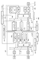
도 1은 제1의 실시예에 따른 화상처리장치의 일례로서의 디지털 카메라의 기능 구성 예를 나타내는 블록도다.
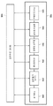
도 2는 제1의 실시예에 따른 화상처리 회로의 기능 구성 예를 나타내는 블록도다.
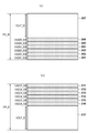
도 3a는 제1의 실시예에 따른 마스터측 화상 프로세서로 처리되는 화상 데이터(상반부)의 예를 나타내는 도면이다.
도 3b는 제1의 실시예에 따른 마스터측 화상 프로세서로 처리되는 화상 데이터(하반부)의 예를 나타내는 도면이다.
도 4는 제1의 실시예에 따른 센서 보정회로에서 실행되는 필터 처리에 사용된 필터 계수의 예를 나타내는 도면이다.
도 5는 제1의 실시예에 따른 코덱(codec) 회로의 기능 구성 예를 나타내는 블록도다.
도 6은 제1의 실시예에 따른 코덱 회로가 처리하는 매크로블록 경계의 구조 예를 나타내는 도면이다.
도 7a는 제1의 실시예에 따른 코덱 회로가 처리하는 화상 데이터의 경계영역의 데이터 예를 화소신호의 단위로 나타내는 도면이다.
도 7b는 제1의 실시예에 따른 코덱 회로가 처리하는 화상 데이터의 경계영역의 데이터 예를 부호화의 블록 단위로 나타내는 도면이다.
도 8은 제2의 실시예에 따른 화상처리 회로의 기능 구성 예를 나타내는 블록도다.
도 9는 데이터 전송 회로와의 관계를 따라서 제2의 실시예에 따른 벡터 검출 회로의 기능 구성 예를 나타내는 도면이다.
도 10은 제2의 실시예에 따른 벡터 검출 회로가 실시한 일련의 동작을 나타내는 흐름도다.
도 11은 제2의 실시예에 따른 벡터 검출 회로가 화상 데이터를 판독하기 위한 그리드 배치와, 특징점, 및 템플릿 매칭 영역의 관계를 나타내는 도면이다.
도 12는 제2의 실시예에 따른, 화상 데이터를 상하부로 분할할 때의 경계영역에 관한 벡터검출 처리 및 데이터 통신처리에 있어서의 일련의 동작을 나타내는 흐름도다.
도 13은 제2의 실시예에 따른 벡터 검출 회로가 처리하는 화상 데이터의 영역을 나타내는 도면이다.
도 14a는 제2의 실시예에 따른 마스터측 화상 프로세서(100)로 처리되는 상반부의 화상 데이터의 예를 나타내는 도면이다.
도 14b는 제2의 실시예에 따른 슬레이브측 화상 프로세서(117)로 처리되는 하반부의 화상 데이터의 예를 나타내는 도면이다.BRIEF DESCRIPTION OF THE DRAWINGS The accompanying drawings, which are incorporated in and constitute a part of the specification, illustrate embodiments of the invention and, together with the description, serve to explain the principles of the invention.
1 is a block diagram showing a functional configuration example of a digital camera as an example of an image processing apparatus according to the first embodiment.
2 is a block diagram showing an example of the functional configuration of the image processing circuit according to the first embodiment.
3A is a diagram showing an example of image data (upper half) processed by the master side image processor according to the first embodiment.
3B is a diagram showing an example of image data (lower half) processed by the master side image processor according to the first embodiment.
4 is a diagram showing an example of filter coefficients used in the filter processing executed in the sensor correction circuit according to the first embodiment.
5 is a block diagram showing a functional configuration example of a codec circuit according to the first embodiment.
6 is a diagram showing an example of the structure of a macroblock boundary processed by the codec circuit according to the first embodiment.
FIG. 7A is a diagram showing an example of data of a boundary region of image data processed by a codec circuit according to the first embodiment, in units of pixel signals. FIG.
7B is a diagram showing an example of data of a boundary area of image data processed by a codec circuit according to the first embodiment in block units of encoding.
8 is a block diagram showing an example of the functional configuration of the image processing circuit according to the second embodiment.
9 is a diagram showing a functional configuration example of the vector detection circuit according to the second embodiment in accordance with the relationship with the data transfer circuit.
10 is a flowchart showing a series of operations performed by the vector detection circuit according to the second embodiment.
11 is a diagram showing the relationship between the grid arrangement for reading image data, the minutiae points, and the template matching area according to the second embodiment of the present invention.
12 is a flowchart showing a series of operations in the vector detection processing and the data communication processing related to the boundary area when the image data is divided into upper and lower portions according to the second embodiment.
13 is a diagram showing an area of image data processed by the vector detection circuit according to the second embodiment.
14A is a diagram showing an example of image data of the upper half portion processed by the master
14B is a diagram showing an example of image data of the lower half processed by the slave
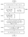
제1의 실시예 First Embodiment
이하, 실시예에 대해서 도면을 참조하여 상세하게 설명한다. 이하에서는, 화상처리장치의 일례로서, 분할한 화상 데이터를 복수의 처리 회로를 사용하여 처리가능한 주어진 디지털 카메라를 설명한다. 그러나, 본 실시예는, 디지털 카메라에 한정하지 않고, 분할한 화상 데이터를 복수의 처리 회로로 처리하는 것이 가능한 임의의 기기에도 적용될 수 있다. 이러한 기기의 예들로서, 퍼스널 컴퓨터, 스마트폰을 포함하는 휴대전화기, 게임기, 타블렛 단말, 시계형이나 안경형의 정보단말, 의료기기, 감시 시스템이나 차재용 시스템의 기기, 데이터 센터에서 동작하는 서버 기기등을 들 수 있다. 이하에서는 분할한 화상 데이터를 복수의 화상 프로세서 중에서 분담해서 처리하는 예를 설명하지만, 본 발명은 복수의 기기나 복수의 가상 머신 중에서 화상 데이터를 분담해서 처리하는 경우에 적용되어도 좋다. Hereinafter, embodiments will be described in detail with reference to the drawings. Hereinafter, a given digital camera capable of processing divided image data using a plurality of processing circuits will be described as an example of the image processing apparatus. However, the present embodiment is not limited to a digital camera, and can be applied to any device capable of processing divided image data by a plurality of processing circuits. Examples of such devices include a personal computer, a mobile phone including a smart phone, a game machine, a tablet terminal, a watch or a glasses type information terminal, a medical instrument, a device of a surveillance system or a vehicle system, . The following describes an example in which divided image data is shared among a plurality of image processors, but the present invention may be applied to a case where image data is shared among a plurality of devices or a plurality of virtual machines.
디지털 카메라150의 구성
Configuration of
도 1을 참조하여, 본 실시예에 따른 디지털 카메라(150)의 기능 구성 예에 대해서 설명한다. 디지털 카메라(150)는, 양쪽이 화상 프로세서인 마스터측 화상 프로세서(100)와 슬레이브측 화상 프로세서(117)를 구비한다. 또한, 마스터측 화상 프로세서(100)와 슬레이브측 화상 프로세서(117)에서 같은 블록들은, 동일 참조번호를 부가하고, 그 중복된 설명을 생략한다. 도 1에 나타낸 예에서는, 마스터측 화상 프로세서(100)와 슬레이브측 화상 프로세서(117)는 다른 구성 요소를 갖지만, 같은 구성을 가져도 좋다.
An example of the functional configuration of the
RAW디코딩 회로(101)는, 매체(111)에 기억된, 압축된 RAW데이터의 신장 처리를 행한다. "RAW 데이터"란, 후술하는 촬상 회로(119)의 촬상 소자로부터 출력된, 1개의 화상을 형성하는 화상신호(화상 데이터)를 AD변환한 R, G, B의 베이어(Bayer) 배열의 데이터다. 화상처리 회로(102)는, 입력된 화상 데이터에 대하여 후술하는 화상 처리를 실시한다. 화상처리 회로(102)에 관한 기능 구성이나 처리 상세에 대해서는 나중에 상세히 설명한다.
The RAW
표시 제어 회로(103)는, 시스템 제어 회로(114)로부터의 지시에 응답하여, 메모리(109)에 기억된 화상 데이터, 조작 메뉴 등의 표시 화상을 표시장치(118)에 표시시킨다. 표시장치(118)는, LCD나, 0LED기기 등으로 구성된 표시 패널을 구비하고, 촬영된 화상이나 디지털 카메라(150)를 조작하기 위한 조작 메뉴 등을 표시한다. 표시장치(118)는, 표시 패널 위에 설치된, 후술하는 조작 부재에 포함되는 터치패널을 가져도 좋다.
The
통신 회로(104)는, 메모리(109)에 기억된 화상 데이터를 한쪽의 화상 프로세서에 송신하고, 또는 한쪽의 화상 프로세서로부터 송신된 화상 데이터를 수신한다. 데이터 전송 회로(105)는, 메모리(109)와 매체(111)에 및 로부터 데이터를 판독해 기록하는, 즉 데이터를 전송하기 위한 복수의 직접 메모리 액세스 제어기(DMAC)로 구성된다.
The
시스템 버스(106)는, 시스템 제어 회로(114), RAW디코딩 회로(101), 화상처리 회로(102), 표시 제어 회로(103), 통신 회로(104), 데이터 전송 회로(105), 메모리 제어 회로(108), 매체 제어 회로(110), 및 불휘발성 메모리 제어 회로(112)를 접속한다. 주 용도는, 시스템 제어 회로(114)로부터 각 처리 블록을 제어할 때에 사용된 버스다.
The
데이터 버스(107)는, 데이터 전송 회로(105), 메모리 제어 회로(108), 및 매체 제어 회로(110)를 접속한다. 주 용도는, 화상 데이터 등의 판독 및 기록시에 사용된 버스다.
The
메모리 제어 회로(108)는, 시스템 제어 회로(114) 혹은 데이터 전송 회로(105)로부터의 지시에 응답하여, 메모리(109)에 데이터를 기록하거나, 메모리(109)로부터 데이터를 판독하거나 한다. 메모리(109)는, 예를 들면, DRAM등으로 구성되고, 소정매수의 정지 화상과 소정 길이의 동화상, 음성등의 데이터나 시스템 제어 회로(114)의 동작에 사용된 변수등을 기억하는데 충분한 기억 용량을 갖는다. 도 1은 마스터측 화상 프로세서(100)와 슬레이브측 화상 프로세서(117)의 각각이 대응하는 메모리(109)와 접속되는 예를 나타내고 있지만, 그 프로세서들이 1개의 공통 메모리를 이용하는 구성이어도 좋다.
The
매체 제어 회로(110)는, 시스템 제어 회로(114)로부터의 지시에 응답하여, 매체(111)에 데이터를 기록하거나, 매체(111)로부터 데이터를 판독하거나 한다. 매체(111)는, 반도체 메모리 등의 기억매체를 포함하고, 압축된 정지 화상이나 동화상 데이터 등을 기억한다.
The
불휘발성 메모리 제어 회로(112)는, 시스템 제어 회로(114)로부터의 지시에 응답하여, 불휘발성 메모리(113)에 데이터를 기록하거나, 불휘발성 메모리(113)로부터 데이터를 판독하거나 한다. 불휘발성 메모리(113)는, 예를 들면 EEPROM등의, 전기적으로 소거/기록 가능한 메모리를 포함하고, 시스템 제어 회로(114)에 의해 실행된 디지털 카메라(150)를 제어하기 위한 프로그램이나 시스템 제어 회로(114)의 동작용의 정수를 기억한다. 도 1은 마스터측 화상 프로세서(100)와 슬레이브측 화상 프로세서(117)의 각각이 대응하는 불휘발성 메모리(113)와 접속되는 예를 나타내고 있지만, 그 프로세서들이 1개의 공통 불휘발성 메모리를 이용하는 구성이어도 좋다.
시스템 제어 회로(114)는, CPU등의 연산용 회로를 구비하고, 디지털 카메라(150)나 마스터측 화상 프로세서(100) 등을 구성하는 각 기능 블록에 대하여 여러가지 지시를 내리거나 각종의 제어 처리를 실행하여서, 디지털 카메라(150) 전체의 동작을 제어한다. 시스템 제어 회로(114)는, 불휘발성 메모리(113)에 기억된 프로그램을 메모리(109)에 로딩하고, 이 프로그램들을 실행하여 본 실시예에 기재된 여러가지의 처리를 실현한다. 또한, 시스템 제어 회로(114)는, 상기 버스들을 통해 각 기능 블록의 동작을 제어한다.
The
통신 데이터 제어 회로(115)는, 시스템 제어 회로(114)에 구비되고, 마스터측 화상 프로세서(100)와 슬레이브측 화상 프로세서(117) 사이에 있어서의 화상 데이터의 교환 명령을 제어한다. 또한, 통신 데이터 제어 회로(115)는, 마스터측 화상 프로세서(100)와 슬레이브측 화상 프로세서(117) 사이에서 화상 데이터를 분할하여 처리시키기 위해서, 처리 대상의 화상 데이터의 분할 사이즈를 산출한다. 또한, 화상 데이터량에 따라서는 마스터측 화상 프로세서(100) 또는 슬레이브측 화상 프로세서(117)만으로 화상 데이터를 처리하여도 된다. 통신 데이터 제어 회로(115)에 의해 행해진 처리에 관한 상세에 대해서는 후술한다.
The communication
조작 부재(116)는, 유저에 의해 조작되는 스위치, 버튼 및 터치패널 등을 포함한다. 조작 부재(116)는, 전원의 ON/OFF, 셔터의 ON/OFF, 메뉴 조작 등의 각종 유저 조작을 검출하여 시스템 제어 회로(114)에 통지한다. 촬상 회로(119)는, 수광한 피사체상을 전기신호로 변환해서 화상 데이터를 생성하는 CCD나 CMOS센서 등의 촬상 소자나, 그 촬상 소자로부터의 아날로그 신호를 디지털 신호로 변환하는 AD변환기등을 포함한다.
The operating
화상처리 회로 102의 구성
The configuration of the
다음에, 도 2를 참조하여, 화상처리 회로(102)의 구성 및 각 회로에 의해 행해진 처리에 대해서 설명한다. 센서 보정회로(201)는, 촬상 소자 또는 데이터 전송 회로(105)로부터 입력된 화상 데이터에 대하여 화소보정, 블랙 레벨 보정, 셰이딩 보정, 결함 보정등의 처리를 실시한다. 센서 보정회로(201)는, 처리한 화상 데이터를 데이터 전송 회로(105), 광학보정회로(202) 또는 그 양쪽에 출력한다. 광학보정회로(202)는, 센서 보정회로(201) 또는 데이터 전송 회로(105)로부터 입력된 화상 데이터에 대하여 배율색수차 보정등의 옵티컬 렌즈에 관한 보정처리를 실시한다. 광학보정회로(202)는, 처리한 화상 데이터를 데이터 전송 회로(105) 또는 현상 처리 회로(203) 또는 그 양쪽에 출력한다.
Next, the configuration of the
현상 처리 회로(203)는, 광학보정회로(202) 또는 데이터 전송 회로(105)로부터 입력된 화상 데이터에 대하여, 감마 보정이나 휘도/색생성 등의 처리를 행한다. 그리고, 현상 처리 회로(203)는, 처리한 화상 데이터를 데이터 전송 회로(105), NR처리 회로(204) 또는 그 양쪽에 출력한다. NR 처리 회로(204)는, 현상 처리 회로(203) 또는 데이터 전송 회로(105)로부터 입력된 화상 데이터에 대하여, 데이터 전송 회로(105)로부터 노이즈 저감(NR)처리된 1프레임앞의 화상 데이터를 입력으로서 취하고, 프레임간의 NR처리를 행한다. NR 처리 회로(204)는, 처리한 화상 데이터를 데이터 전송 회로(105), 기하학 변형 회로(205), 또는 그 양쪽에 출력한다. 화상 데이터의 입력은, 데이터 전송 회로(105)로부터 2화상분의 데이터를 동시에 입력해도 좋다. 기하학 변형 회로(205)는, NR처리 회로(204) 또는 데이터 전송 회로(105)로부터 입력된 화상 데이터에 대하여, 기하변형 처리, 예를 들면 옵티컬 렌즈의 왜곡을 제거하는 왜곡보정등의 처리를 행한다. 기하학 변형 회로(205)는, 처리한 화상 데이터를 데이터 전송 회로(105), 코덱 회로(206), 또는 그 양쪽에 출력한다.
The
코덱 회로(206)는, 기하학 변형 회로(205) 또는 데이터 전송 회로(105)로부터 입력된 화상 데이터를 JPEG형식이나 MPEG형식등으로 압축 부호화한다. 혹은, 압축 부호화된 화상 데이터가 입력되었을 경우, 코덱 회로(206)는, 그 부호화된 화상 데이터에 대하여 신장 처리를 행해서 비압축의 화상 데이터를 작성하여, 데이터 전송 회로(105)에 출력한다. 또한, 코덱 회로(206)의 처리를 상세히 후술한다.
The
화상을 분할해서 처리할 경우에 필요한 화상 데이터의 예 Example of image data required for dividing and processing an image
다음에, 도 3a 및 도 3b를 참조하여, 분할한 화상 데이터(본 예에서는, 상하 2분할)를 복수의 화상 프로세서에 입력할 경우에, 각 화상처리 블록이 실행한 처리를 위해서 필요한 데이터량에 대해서 설명한다. Next, with reference to Figs. 3A and 3B, when inputting the divided image data (upper and lower halves in this example) to a plurality of image processors, the amount of data necessary for processing executed by each image processing block .
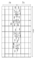
도 3a는, 마스터측 화상 프로세서(100)로 처리된, 화상의 상반부의 화상 데이터를 나타낸다. 또한, 도 3b는, 슬레이브측 화상 프로세서(117)로 처리된, 화상의 하반부의 화상 데이터를 나타낸다. 도 3a에 있어서, VIN_M은 마스터측 화상 프로세서(100)의 화상처리 회로(102)에 입력된 화상 데이터의 라인수를 나타내고, 영역307로 나타낸 VOUT_M이 화상 데이터의 출력 라인수를 나타낸다.
Fig. 3A shows image data of the upper half of the image processed by the master
VADD1_M은, 화상처리 회로(102)의 센서 보정회로(201)에 의해 실시된 처리에서 사용된 후, 삭제되는 화상 데이터 영역(301)의 라인수를 나타낸다. VADD2_M 및 VADD3_M은, 각각, 광학보정회로(202) 및 현상 처리 회로(203)에 의해 실시된 처리에서 사용된 후에 삭제되는 화상 데이터 영역(302 및 303)을 나타낸다. 마찬가지로, VADD4_M, VADD5_M 및 VADD6_M은, 각각 NR처리 회로(204), 기하학 변형 회로(205), 코덱 회로(206)에 의해 처리된 후 삭제되는 화상 데이터 영역(304∼306)의 라인수를 나타낸다. 또한, 도 3b에 나타낸, 슬레이브측 화상 프로세서(117)의 화상처리 회로(102)에서 처리된 화상 데이터에 대해서는 후술한다.
VADD1_M represents the number of lines of the
도 4는, 본 실시예에 따른 센서 보정회로(201)에서 실시된 필터 처리에 사용된 필터 계수의 예를 나타내는 도면이다. 센서 보정회로(201)는, 9×9 탭 필터 계수를 가진다. 센서 보정회로(201)는, 현상 처리 회로(203)에 입력되는 화상 데이터의 처리 대상 화소의 화소값p(x, y)와, 처리 대상 화소를 중심으로 하는 9×9주변화소로 구성된 참조 화소를 사용하고, 식(1)에 나타내는 연산을 실시하고, 화소값q(x, y)를 출력한다.
4 is a diagram showing an example of filter coefficients used in the filter processing performed by the
![]()
![]()
본 예에서는, 센서 보정회로(201)에 입력된 화상 데이터의 라인수 VIN_M에 대하여, 종단의 4라인분에 관해서는, 필터 처리에서 사용된 하단측의 참조 화소가 존재하지 않는다. 이 때문에, 센서 보정회로(201)는, 필터 처리를 실시할 수 없다. 그 결과, 센서 보정회로(201)로부터 출력된 화상 데이터의 라인수는, (VIN_M-4)라인이거나, 다시 말해, VADD1_M=4이 된다.
In this example, with respect to the number of lines VIN_M of the image data input to the
도 4에 나타낸 필터 처리를 실시하는 경우에, 상단측에서 4라인분, 좌우단측에서 4화소분에 대해서는 참조 화소가 존재하지 않아, 필터 처리를 실시할 수 없다. 이 때문에, 입력 화상 데이터의 사이즈보다, 출력 화상 데이터의 사이즈가 작다. 또한, 이하의 설명에서는, 화상이 상하부로 분할될 때 생기는 경계부분의 라인수에 대해서만 기술한다. 이들 "경계부분"은, 마스터측 화상 프로세서(100)의 처리 동안에 화상 데이터의 하단에 해당하고, 슬레이브측 화상 프로세서(117)에 대해서는 화상 데이터의 상단에 해당한다.
In the case of performing the filter processing shown in Fig. 4, there are no reference pixels for four lines on the upper side and for four pixels on the left and right side, and filter processing can not be performed. Therefore, the size of the output image data is smaller than the size of the input image data. In the following description, only the number of lines of the boundary portion generated when an image is divided into upper and lower portions is described. These "boundary portions" correspond to the lower end of the image data during the processing of the master
또한, 마스터측 화상 프로세서(100)의 광학보정회로(202)에서 실시한 처리에서는 VADD2_M=9라인분이 필요하다. 추가로, 현상 처리 회로(203)에서 실시된 처리에서는 VADD3_M=13라인, NR처리 회로(204)에서 실시된 처리에서는 VADD4_M=11라인, 기하학 변형 회로(205)에서 실시된 처리에서는 VADD5_M=135라인이 필요하다. 코덱 회로(206)에서 실시된 처리에서는 VADD6_M=4라인분이 필요하다. 따라서, VADD1_M으로부터 VADD6_M까지의 총 라인수로서 192라인이 필요하다.
In the processing performed by the
예를 들면, 별도로 도 7a 및 도 7b를 참조하여 후술하는 것 같은, 처리 도중의 데이터를 각 화상 프로세서간에 전송하는 구성이 아닐 경우, 상술한 192라인분의 여분의 데이터를 처리하는 것이 필요하다. 다시 말해, 출력 화상 데이터로서 VOUT_M라인분의 데이터를 확보하기 위해서, 우선 (VOUT_M+192)라인분의 입력 화상 데이터를 화상처리 회로(102)에 입력할 필요가 있다. 그리고, 화상처리 회로(102)의 각 처리 회로로 삭제된 화상 데이터도 전단의 처리 회로에 있어서 처리할 필요가 있다.
For example, when the data during processing is not transferred between the respective image processors, as will be described later with reference to Figs. 7A and 7B separately, it is necessary to process the above-mentioned extra data for 192 lines. In other words, input image data for (VOUT_M + 192) lines must first be input to the
다시 도 3b를 참조하여, 슬레이브측 화상 프로세서(117)의 화상처리 회로(102)가 사용하는 화상 데이터에 대해서 설명한다. 도 3b에서는, VIN_S는 슬레이브측 화상 프로세서(117)의 화상처리 회로(102)에 입력된 화상 데이터의 라인수를 나타낸다. 한편, 영역 317로 나타낸 VOUT_S는 출력되는 화상 데이터의 라인수를 나타낸다.
3B, the image data used by the
도 3b에서, VADD1_S는, 센서 보정회로(201)에 의한 처리후에 삭제되는 화상 데이터 영역의 상단의 라인수를 나타낸다. 마찬가지로, VADD2_S는 광학보정회로(202), VADD3_S는 현상 처리 회로(203)의 처리후에 삭제된 화상 데이터 영역(312, 313)을 나타낸다. VADD4_S는 NR처리 회로(204), VADD5_S는 기하학 변형 회로(205), VADD6_S는 코덱 회로(206)의 처리후에 삭제된 화상 데이터 영역(314∼316) 하단의 라인수를 나타낸다.
3B, VADD1_S represents the number of lines at the top of the image data area to be deleted after processing by the
마스터측의 처리에 있어서 상술한 것 같이, 각 화상 프로세서간에 처리 도중의 데이터를 전송하지 않을 경우, VADD1_S로부터 VADD6_S까지의 총 라인수인 192라인의 데이터가 필요하다. 다시 말해, 처리 도중의 데이터를 각 화상 프로세서간에 전송하지 않을 경우, 마스터측 화상 프로세서(100) 및 슬레이브측 화상 프로세서(117)는, 각각이 처리하는 동일한 화상 데이터 영역을 중복하여 처리하는 것이 필요하다.
As described above in the processing on the master side, when data during processing is not transferred between the respective image processors, data of 192 lines, which is the total number of lines from VADD1_S to VADD6_S, is required. In other words, when data during processing is not transferred between the respective image processors, it is necessary for the master-
코덱 회로(206)의 구성과 각 회로의 동작
The configuration of the
도 5는, 본 실시예에 따른 코덱 회로(206)의 구성을 나타낸다. 움직임 예측 회로(501)는, 상술한 상하 분할된 상측의 화상 데이터를, (예를 들면 데이터 전송 회로(105)로부터) 매크로 블록 단위로 클러스터순으로 취득한다. 움직임 예측 회로(501)는, 부호화 대상 화상과, 참조 프레임 버퍼(510)로부터 입력된 참조 화상과의 사이에서 블록 매칭을 실시하여, 움직임 벡터 검출을 실시한다. 움직임 예측 회로(501)는, 부호화 대상 화상과 검출된 움직임 벡터 위치의 참조 화상과의 사이에서 화소의 차분을 찾고, 그 차분 화상을 이산 코사인 변환회로(502)에 출력한다. 이산 코사인 변환회로(502)는, 입력된 차분 화상에 대하여 이산 코사인 변환을 실시하고, 변환 계수를 생성하고, 양자화 회로(503)에 출력한다. 양자화 회로(503)는, 보내져 온 변환 계수에 대하여, 양자화 제어 회로(504)가 출력한 양자화 파라미터에 따라서 양자화한다. 양자화된 변환 계수는 엔트로피 부호화 회로(505), 및 국소적으로 디코딩된 화상을 작성하기 위한 역양자화 회로(506)에 출력된다. 엔트로피 부호화 회로(505)는, 양자화후의 변환 계수에 대하여 가변길이 부호화를 실시한다. 엔트로피 부호화 회로(505)는, 이것에 움직임 벡터들, 양자화 파라미터들, 및 매크로블록 분할 정보등의 가변길이 부호화된 부호화 방식정보를 부가하여, 부호화 스트림을 생성한다. 또한, 부호화시에 매크로블록마다 발생된 부호량을 산출하고, 양자화 제어 회로(504)에 출력한다.
5 shows a configuration of a
양자화 제어 회로(504)는, 양자화 파라미터를 결정한다. 양자화 제어 회로(504)는, 부호화를 행하는 해당 매크로블록이 화상의 분할 경계에 접하고 있는 것인가 아닌가를 나타내는 정보(화상의 경계정보)를 취득한다. 부호화를 행하는 매크로블록이 화상의 분할 경계에 접하지 않고 있는 경우에는, 양자화 제어 회로(504)는, 엔트로피 부호화 회로(505)로부터 발생된 부호량을 취득하고, 목표 부호량이 되도록 양자화 파라미터를 결정하여, 양자화 회로(503)에 출력한다. 역양자화 회로(506)는, 입력된 양자화후의 변환 계수에 대하여 역양자화를 실시하고, 로컬 디코딩 변환 계수를 생성한다. 이 변환 계수들은, 역이산 코사인 변환회로(507)에 출력된다. 역이산 코사인 변환회로(507)는, 입력된 변환 계수에 대하여 역이산 코사인 변환을 실시하여, 차분 화상을 생성한다. 그 차분 화상은, 움직임 보상 회로(508)에 출력된다. 움직임 보상 회로(508)는, 움직임 벡터 위치의 참조 화상을 참조 프레임 버퍼(510)로부터 판독하고, 입력된 차분 화상을 가산하여 국소적으로 디코딩된 화상 데이터를 생성한다.
The
움직임 보상 회로(508)에 의해 생성된 화상 데이터는, 디블록킹 필터(509)에 출력된다. 디블록킹 필터(509)는, 입력된 화상 데이터에 대하여 디블록킹 필터를 적용한다. 디블록킹 필터후의 화상이 국소적으로 디코딩된 화상으로서 참조 프레임 버퍼(510)에 기억된다.
The image data generated by the
이렇게 하여 코덱 회로(206)는, 부호화 스트림 및 국소적으로 디코딩된 화상을 생성한다. 또한, 디블록킹 필터(509)는, 예를 들면 H.264부호화 방식에 근거한 디블록킹 필터 처리를 실시한다. 단, 실제로 블록 경계에 필터 처리를 실시할 것인가 아닌가는, 해당 블록 경계의 화소값이나 부호화 파라미터 등에 의해 결정된다.
In this way, the
도 6은, 본 실시예에 따른 코덱 회로(206)가 처리한 매크로블록 경계의 구성을 나타낸다. 601로 나타낸 수평방향의 블록 경계에서, 화소값p0∼q3으로 구성된 블록 및 화소값q0∼q3으로 구성된 블록은 서로 인접하고 있다. 마찬가지로, 602로 나타낸 수직방향의 블록 경계에서, 화소값p0∼q3으로 구성된 블록 및 화소값q0∼q3으로 구성된 블록은 서로 인접하고 있다.
6 shows the structure of the macro-block boundary processed by the
H.264부호화 방식에 근거한 규격의 경우에, 코덱 회로(206)는 이하의 식(2)로 나타낸 조건이 충족될 때에 블록 경계에 디블록킹 필터 처리를 실시한다.
In the case of the standard based on the H.264 coding method, the
Bs>0 Bs> 0
|p0-qO|<α 및 |p1-qO| <β 및 |q1-q0| <β ...(2) | P0-qO | <? And | p1-qO | <? And | q1-q0 | <? ...(2)
여기서, Bs(boundary strength)값은 화상의 블록 경계의 강도를 나타내는 수치이며, p, q는 인트라(화면내)/매크로블록 관계에 의해 결정된 수치다. α, β는 각각 IndexA, IndexB의 값에 대한 테이블로 정의된다. IndexA, IndexB는, 양자화 파라미터 및 필터 강도에 대한 오프셋 값으로부터 산출된다. Here, the value of Bs (boundary strength) is a numerical value indicative of the strength of the block boundary of the picture, and p and q are values determined by the intra (in-picture) / macroblock relationship. ?,? are defined as a table for the values of IndexA and IndexB, respectively. IndexA and IndexB are calculated from the offset values for the quantization parameter and the filter strength.
Bs <4의 경우에는, 입력을 p1, pO, qO, q1으로서, 4탭의 FIR필터의 처리에 의해 p'0과 q'0(p'0은 pO, q'0은 qO의 디블록킹 필터 처리를 통해 얻어진 화소값)이 생성된다. 한편, |p2-pO|<β의 경우에는, 입력을 p2, p1, pO, q1으로서, 4탭의 FIR필터의 처리에 의해, p'1(p'1은 p1의 디블록킹 필터 처리를 통해 얻어진 화소값)이 생성된다. 또한, |q2-qO|<β의 경우에는, 입력을 q2, q1, q0, p1으로서, 4탭의 FIR필터의 처리에 의해, q'1(q'1은 q1의 디블록킹 필터 처리를 통해 얻어진 화소값)이 생성된다. In the case of Bs < 4, the inputs are p1, pO, qO, and q1, and by the processing of the 4-tap FIR filter, p'0 and q'0 (p'0 is pO, q'0 is qO Pixel value obtained through processing) is generated. On the other hand, in the case of | p2-p0 | <?, the input is p2, p1, pO, q1 and the p1 The obtained pixel value) is generated. In the case of | q2-qO | <?, The input is q2, q1, q0, and p1, and q'1 (q'1 is processed through deblocking filter processing of q1) The obtained pixel value) is generated.
Bs=4의 경우에는, 이하의 처리가 실시된다. |p2-p0|<β 및 |p0-p0| <α/4+2의 경우, 입력을 p2, p1, p0, q0, q1으로서, 5탭의 FIR필터의 처리에 의해 p'0이 생성된다. 또한, 입력을 p2, p1, p0, q1으로서, 4탭의 FIR필터의 처리에 의해 p'1이 생성된다. 휘도신호의 경우에, 입력을 p3, p2, p1, p0, q0로서, 5탭의 FIR필터의 처리에 의해 p'2가 생성된다. 그 이외의 경우에는, 입력을 p1, p0, q1으로서, 3탭의 FIR필터의 처리에 의해 p'0이 생성된다. When Bs = 4, the following processing is performed. In the case of | p2-p0 | <? And | p0-p0 | <? / 4 + 2, p'0 is generated by processing the FIR filter of 5 taps with p2, p1, p0, q0 and q1 as inputs . In addition, p'1 is generated by the processing of the 4-tap FIR filter with inputs p2, p1, p0 and q1. In the case of the luminance signal, the input is p3, p2, p1, p0, q0, and p'2 is generated by the processing of the 5-tap FIR filter. In the other cases, p'0 is generated by the processing of the 3-tap FIR filter with inputs p1, p0, and q1.
|q2-q0| <β 및 |p0-p0| <α/4+2의 경우, 입력을 q2, q1, q0, p0, p1으로서, 5탭의 FIR필터의 처리에 의해 q'0이 생성된다. 한편, 입력을 q2, q1, q0, p0으로서, 4탭의 FIR필터의 처리에 의해 q'1이 생성된다. 휘도신호의 경우, 입력을 q3, q2, q1, q0, p0로서, 5탭의 FIR필터의 처리에 의해 q'2가 생성된다. 그 이외의 경우에는, 입력을 q1, q0, p1으로서, 3탭의 FIR필터의 처리에 의해 q'0이 생성된다. In the case of | q2-q0 | <? And | p0-p0 | <? / 4 + 2, q'0 is generated by the processing of the 5-tap FIR filter with the inputs q2, q1, q0, p0 and p1 . On the other hand, as inputs q2, q1, q0 and p0, q'1 is generated by the processing of the 4-tap FIR filter. In the case of the luminance signal, the input is q3, q2, q1, q0, and p0, and q'2 is generated by the processing of the FIR filter of the five taps. In the other cases, q'0 is generated by the processing of the 3-tap FIR filter with inputs q1, q0, and p1.
본 실시예에 따른 화상의 분할과 프로세서간의 통신 처리 The division of the image according to the present embodiment and the communication processing between the processors
다음에, 본 실시예에 따른 화상의 분할과 프로세서간의 처리에 대해서 설명한다. 다시 말해, 본 실시예에서는, 각 프로세서에 입력하는 화상 데이터의 양을 삭감하기 위해서, 도 3a 및 도 3b를 참조해서 설명한 화상 분할 대신에, 이하에 설명하는 화상의 분할을 실시한다. 이 화상의 분할에 의해, 화상처리 회로(102)내의 각 블록에 있어서의 처리가 진행함에 따라서 프로세서간에 통신을 요하지만, 공통의 통신방법이 사용된다. 이 때문에, 블록마다 예들로서 코덱 회로(206)의 처리와, 코덱 회로(206)의 처리에 대응한 프로세서간 통신을 설명한다.
Next, the division of the image and the processing between the processors according to the present embodiment will be described. In other words, in the present embodiment, in order to reduce the amount of image data to be input to each processor, the image division described below is performed instead of the image division described with reference to Figs. 3A and 3B. As the processing in each block in the
도 7a는, 마스터측 화상 프로세서(100)에 포함된 코덱 회로(206)가 처리하는 화상 데이터의 경계영역을 화소단위로 나타낸다. 도 7a에서, 각 4각형은 개개의 화소를 나타낸다. 도 7b는, 코덱 회로(206)가 처리하는 화상 데이터의 경계영역을 부호화의 블록 단위로 나타내는 도면이다. 도 7b에 나타낸 각 4각형은, 도 7a에서 나타낸 4×4화소의 부호화 블록을 나타낸다. 도 7a 및 도 7b에 나타낸 점선701은, 화상 데이터를 상/하 분할할 때의 경계를 나타낸다. 마스터측 화상 프로세서(100)가 점선701보다 상측의 화상 데이터를 처리하는 한편, 슬레이브측 화상 프로세서(117)가 점선701보다 하측의 화상 데이터를 처리한다. 본 실시예에서는, 1개의 화상을, 2개의 화상 프로세서에 입력된 동일한 화소 데이터 영역이 존재하지 않도록 분할한다. 다시 말해, 도 3a 및 도 3b에 나타낸 예를 사용하여, VADD6_M=0, VADD6_S=0이다.
7A shows the boundary area of the image data processed by the
마스터측 화상 프로세서(100)의 디블록킹 필터(509)가 영역702에 포함된 블록들을 처리할 경우, 상술한 것처럼, 인접한 하측의 화상 데이터에 있어서의 소정의 범위에 대응한 영역703의 블록들이 필요하다. 이에 따라, 마스터측 화상 프로세서(100)의 디블록킹 필터(509)는, 슬레이브측 화상 프로세서(117)의 통신 회로(104)로부터 영역703의 블록들을 취득하여, 블록 경계의 디블록킹 필터 처리를 실행한다. 또한, 마스터측 화상 프로세서(100)와 슬레이브측 화상 프로세서(117)간의 통신(화상 데이터의 전송)은, 통신 데이터 제어 회로(115)의 제어하에 실행된다. 영역703의 블록들은, 슬레이브측 화상 프로세서(117)에 있어서 기하학 변형 회로(205)까지의 같은 처리가 실행되므로, (마스터측의) 코덱 회로(206)에 의해 디블록킹 필터 처리가 연속될 수 있다.
When the
한편, 슬레이브측 화상 프로세서(117)의 디블록킹 필터(509)가 영역703에 포함된 블록들을 처리할 경우, 인접한 상측의 화상 데이터에 있어서의 소정의 범위에 해당한 영역702내의 블록들이 필요하다. 이에 따라, 마스터측 화상 프로세서(100)의 통신 회로(104)로부터, 영역702에의 디블록킹 필터 처리가 완료된 블록들을 취득하고, 상/하 분할에 해당하는 블록 경계에 디블록킹 필터 처리를 실시한다. 영역702의 블록들은, 영역703과 같이, 마스터측 화상 프로세서(100)에 있어서 기하학 변형 회로(205)까지 같은 화상처리가 실행되므로, (슬레이브측의) 코덱 회로(206)에 의해 디블록킹 필터 처리가 연속될 수 있다. 또한, 디블록킹 필터는 모든 블록 경계에 적용되지 않으므로, 상기 필터가 적용되는 개소의 블록들만 각 화상 프로세서간에 전송되어도 좋다.
On the other hand, when the
이상 설명한 바와 같이, 본 실시예에 의하면, 1개의 화상을 마스터측 화상 프로세서(100)와 슬레이브측 화상 프로세서(117) 사이에서 분담해서 처리할 경우에, 동일한 영역을 갖지 않는 화상 데이터를 각 프로세서에 입력한다. 그리고, 화상처리의 각 단계가 진행함에 따라, 각각의 단계에서 추가적으로 필요한 경계부근의 화상 데이터를, 프로세서간에 통신한다. 이렇게 함으로써, 각 프로세서의 화상처리 회로(102)내의 각 블록에서 처리한 소정의 라인수(예를 들면, 코덱 회로(206)의 경우에, 도 3a에 나타낸 것처럼, VADD6_M=4)를 제거할 수 있다. (예를 들면, VADD6_M의) 라인의 데이터를 제거함으로써, 처리의 전단에서, 즉 센서 보정회로(201)로 기하학 변형 회로(205)에 있어서의 여분의 영역에 대한 처리가 불필요해져, 처리 시간을 단축하고 전력 소비를 감소할 수 있다.
As described above, according to the present embodiment, when one image is shared between the master
제2의 실시예 Second Embodiment
다음에, 제2의 실시예에 대해서 설명한다. 제2의 실시예에서는, 화상처리 회로(102)가 움직임 벡터를 검출하는 벡터 검출 회로를 구비하고, 해당 벡터 검출 회로에 의한 움직임 벡터의 검출 처리에 있어서 분할 경계에 걸친 필요한 데이터를 취득하는 구성을 설명한다. 제2의 실시예에 따른 디지털 카메라(150)의 구성은, 화상처리 회로(102)의 내부 회로 구성의 일 회로외에는, 제1의 실시예에 따른 디지털 카메라(150)의 구성과 같다. 이에 따라, 대응한 구성요소는 동일한 참조부호를 부착하고, 중복 설명은 생략하고, 차이점에 대해서 중점적으로 설명한다.
Next, the second embodiment will be described. In the second embodiment, the
화상처리 회로(102)의 구성
The configuration of the
우선, 도 8을 참조하여, 본 실시예에 따른 화상처리 회로(102)의 구성을 설명한다. 제1의 실시예와 같이, 현상 처리 회로(203)가 처리한 화상 데이터는, NR처리 회로(204), 데이터 전송 회로(105) 또는 그 양쪽에 출력된다. NR처리 회로(204)가 처리한 화상 데이터는, 데이터 전송 회로(105), 축소 처리 회로(801) 또는 그 양쪽에 출력된다.
First, the configuration of the
축소 처리 회로(801)는, 미리 설정된 비율에 따라서 화상 데이터의 축소 처리를 실시하고, 축소한 화상 데이터를 데이터 전송 회로(105)에 출력한다. 축소된 화상 데이터는, 데이터 전송 회로(105)를 거쳐 벡터 검출 회로(802)에 입력된다. 벡터 검출 회로(802)는, 현재의 프레임과, 현재의 프레임 앞의 프레임간에 템플릿 매칭을 실시하여, 각 점(각 좌표위치)에 있어서의 벡터 데이터를 검출한다. 검출한 벡터 데이터는 동화상 데이터에 대한 안정화등의 처리에 사용된다.
The
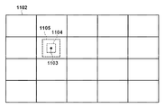
다음에, 벡터 검출 회로(802)의 처리에 대해서 설명한다. 우선, 도 11은, 벡터 검출 회로(802)가 판독하는 그리드 배치와 템플릿 영역등의 관계를 나타내고 있다. 다시 말해, 소정의 사이즈의 그리드(1102)는, 수평 및 수직방향으로, 그의 설정된 개수가 설치되도록 배치된다(도 11에 나타낸 예에서는, 총 20개의 그리드, 즉 5개의 수평 그리드와 4개의 수직 그리드가 배치되어 있다). 각 그리드에서는, 특징점(1103)이 하나 추출되고, 이 특징점(1103)을 중심으로 하여, 사각형이고 설정된 사이즈를 갖는 서치 영역(1105) 및 템플릿 영역(1104)이 설정된다.
Next, the processing of the
벡터 검출 회로(802)에 의해 행해진 구성 및 일련의 동작
The configuration and sequence of operations performed by the
도 9 및 도 10을 참조하여, 벡터 검출 회로(802)가 행하는 벡터 검출 처리의 개요를 설명하면서, 벡터 검출 회로(802)의 기능 구성 예를 설명한다. 또한, 이하의 일련의 동작은, 시스템 제어회로(114)가 불휘발성 메모리(113)에 기억된 프로그램을 로딩 및 실행하고, 그 프로세서들을 구성하는 각 회로 혹은 통신 데이터 제어 회로(115)를 제어함으로써, 실시된다. 추가로, 벡터 검출 회로(802)에 의해 행해진 처리는, 예를 들면 분할된 입력 화상 데이터가, 데이터 전송 회로(105)의 RDDMAC 1(921)에 입력될 수 있는 경우에 개시된다.
An example of the functional configuration of the
S10O1에 있어서, 판독을 제어하는 RDDMAC 1(921)은, 벡터 검출 대상이 되는 현 프레임의 입력 화상 데이터(941)를, 도 11에 나타낸 소정의 그리드(1102)의 사이즈마다 메모리(109)로부터 판독한다. 메모리(109)에 기억된 입력 화상 데이터(941)는, 상술한 화상처리 회로(102)내의 각 블록에 의해 행해진 상술한 화상처리가 실행된다. RDDMAC 1(921)에 의해 그리드 단위로 판독된 입력 화상 데이터(941)는, 후단 블록의 템플릿 매칭용 화상생성 회로(901)와 특징점 산출 회로(902)에 출력된다.
The
S10O2에 있어서, 템플릿 매칭용 화상생성 회로(901)는, 벡터 검출시에 템플릿 매칭에 사용된 템플릿 매칭용 화상을 생성하여, 기록을 제어하는 WRDMAC 1(931)에 출력한다. 템플릿 매칭용 화상생성 회로(901)는, 예를 들면 밴드패스필터 회로를 구비하고, 템플릿 매칭 처리에 불필요한 화상신호의 고주파성분과 저주파성분을 차단한다. 또한, 템플릿 매칭 처리에서 실시된 연산량을 삭감하기 위해서, 템플릿 매칭용 화상생성 회로(901)는 입력 화상 데이터에 대하여 2값화 처리를 실시한다. 구체적으로는, 입력 화상 데이터(941)가 14비트의 비트 심도를 가지는 휘도 데이터일 경우, 그 밴드패스필터 회로에 의한 필터 처리에서는, 해당 휘도 데이터는 역치 판정을 통해 1비트의 비트 심도를 가지는 2값 데이터로 변환된다.
In S10O2, the template matching
S10O3에 있어서, WRDMAC 1(931)은, 입력된 템플릿 매칭용 화상 데이터1(942)을 기록하는 처리를 실시한다. 한편, 메모리(109)에는 이전 프레임에서 생성된 템플릿 매칭용 화상 데이터2(943)가 기억되어 있다. 상술한 것 같이, 템플릿 매칭용 화상 데이터1(942)과 템플릿 매칭용 화상 데이터2(943)는 2값 데이터다.
In S10O3, the
S10O4에 있어서, 특징점 산출 회로(902)는, S1002 및 S1003의 처리와 병렬하여, 현 프레임으로부터의 그리드 단위의 화상 데이터에 대하여 특징점 산출 처리를 실시한다. 특징점 산출 회로(902)는, 특징 필터 회로, 특징평가 회로, 및 특징점 결정 회로를 구비한다. 특징 필터 회로는, 밴드패스필터, 수평미분 필터, 수직미분 필터, 및 평활화 필터등의, 복수의 필터로 구성된다. 특징 필터 회로는, 예를 들면 밴드패스필터를 사용해서 화상신호로부터 불필요한 고주파성분과 저주파성분을 절단하고, 수평방향의 미분 필터를 적용해서 얻어진 신호와, 수직방향의 미분 필터를 적용해서 얻어진 신호의 각각에 평활화 필터 처리를 적용한다. 더욱, 특징평가 회로는, 특징 필터 회로에 의해 필터 처리된 그리드에 대하여, 화소마다 2개의 엣지의 교점들이나 곡률이 극대가 되는 곡선형의 점들등의, 화소의 주변의 미분값이 다방향으로 큰 점을, 특징 평가식을 사용해서 평가 함에 의해, 특징값을 산출한다. 본 실시예에 따른 특징평가 회로에 의해 실시된 처리의 일례로서 Shi and Tomasi의 수법에 대해서 설명한다. 우선, 특징점 산출 회로(902)는, 수평미분 필터와 수직미분 필터를 적용한 결과로부터, 자기상관 행렬H를 작성한다. 자기상관 행렬H의 식을, 식(3)에 나타낸다.
In S10O4, the minutiae

식(3)에서는, Ix는 수평미분 필터를 적용한 결과를 나타내고, Iy는 수직미분 필터를 적용한 결과를 나타내고, 가우시안 필터G와 컨볼브(convolve)한다. 다음에, 특징점 산출 회로(902)는, 식(4)에 나타낸 Shi and Tomasi의 특징 평가식을 산출한다.
In equation (3), Ix represents the result of applying the horizontal differential filter, Iy represents the result of applying the vertical differential filter, and convolve the Gaussian filter G. Next, the feature
Shi and Tomasi=min(λ1, λ2) (4) Shi and Tomasi = min (? 1,? 2) (4)
식(4)는, 식(3)에 나타낸 자기상관 행렬H의 고유값 λ1, λ2 중 작은쪽의 고유값을 특징값으로서 나타낸다. Equation (4) shows, as a characteristic value, the smaller eigenvalue of the eigenvalues? 1 and? 2 of the autocorrelation matrix H shown in the equation (3).
특징점 결정 회로는, 특징평가 회로에 의해 화소마다 산출된 그리드내에 있어서 가장 큰 특징값을 갖는 화소를 특징점으로서 결정한다. 이 결정된 특징점은, 특징점 산출 회로(902)의 내부 메모리나 레지스터에 그리드마다 기억된다. 해당 메모리나 레지스터는, 이전 프레임의 특징점과 현 프레임의 특징점을 기억하기 위한 용량을 가지고 있다. 그리고, 특징점 결정 회로는, 대응하는 그리드의 템플릿 매칭 처리가 개시될 때에, 이전 프레임에서 산출된 특징점을 특징점 좌표정보(951)로서 RDDMAC 2(922)에 입력한다.
The feature point determination circuit determines, as feature points, a pixel having the largest feature value in the grid calculated for each pixel by the feature evaluation circuit. The determined minutiae points are stored in the internal memory or registers of the minutiae
S1005에 있어서, RDDMAC 2(922)는, 소정의 사이즈의 사각형 영역을, 현 프레임에서 생성된 템플릿 매칭용 화상 데이터1 및 이전 프레임에서 생성된 템플릿 매칭용 화상 데이터2로부터 판독한다. 소정의 사이즈의 사각형영역은, 입력된 이전 프레임에서 산출된 특징점 좌표정보(951)에 근거하여, 특징점(1103)을 중심으로 한 영역으로서 추출된다. 또한, 템플릿 매칭용 화상 데이터1로부터 서치 영역(1105)을 판독하고, 이전 프레임에서 생성된 템플릿 매칭용 화상 데이터2로부터 템플릿 영역(1104)을 판독한다. 판독된 화상 데이터는, 각각, 서치 영역 화상 데이터(953) 및 템플릿 영역 화상 데이터(954)로서, 템플릿 매칭 처리 회로(903)에 입력된다.
In step S1005, the
S1006에 있어서, 템플릿 매칭 처리 회로(903)는, 입력된 서치 영역 화상 데이터(953)와 템플릿 영역 화상 데이터(954)간의 상관 값을 산출하고, 산출한 상관 값에 근거해서 벡터 값을 산출한다. 본 실시예에서는, 상관 값의 산출 방법으로서, 예를 들면 차분 절대치합(이하, "SAD"로 약칭한다)을 구한다.
In step S1006, the template

여기서, f(i j)은 템플릿 영역 화상 데이터(954)내의 좌표(i j)에 있어서의 화소값을 나타내고, g(i j)는 서치 영역 화상 데이터(953)에 있어서 상관 값 산출의 대상이 되는 영역내의 화소값을 나타낸다. 상관 값 산출 대상영역은, 템플릿 영역 화상 데이터(954)와 같은 크기다. SAD에 의하면, 각각의 영역내의 각 화소값f(i j)와 g(i j)간의 차이의 절대치를 계산하고, 그 합을 구하여 상관 값S_SAD를 얻는다. 따라서, 상관 값S_SAD의 값이 작을 수록 영역간의 휘도값의 차이가 작고, 각각의 상관 값 산출 영역내의 텍스쳐가 유사한 것을 나타낸다. 바꾸어 말하면, 상관 값S_SAD가 가장 작은 변화의 정도를 구하는 것에 의해, 화상간에 대응하는 영역을 탐색할 수 있다. 이 때, 서치 영역 화상 데이터(953)와 템플릿 영역 화상 데이터(954)는 1비트의 2값 데이터이기 때문에, 상관 값S_SAD를 구하기 위해 적은 연산량만이 요구되는 이점이 있다. 또한, 본 실시예에서는, 상관 값의 일례로서 SAD를 사용하고 있지만, 상기 방법은 이에 한정되지 않는다. 차분제곱합(SSD)이나 정규화 상호상관(NCC)등의 다른 상관 값도 사용해도 좋다. 템플릿 매칭 처리 회로(903)는, 상관 값이 최소값이 되는 위치에 근거해서 그리드의 움직임 벡터를 산출하고, 산출한 벡터 정보(955)를 WRDMAC 2(932)에 출력한다.
Here, f (ij) represents the pixel value in the coordinate (ij) in the template
S1007에 있어서, WRDMAC 2(932)는, 데이터 버스(107)를 통해 메모리(109)에 그 벡터 정보(955)를 기록한다. 벡터 검출 회로(802)는, WRDMAC 2(932)에 의한 벡터 정보(955)의 메모리(109)에의 기록이 종료하면, 움직임 벡터 검출 처리를 종료한다. 상술한 처리에서는 1프레임분의 처리를 설명했지만, 각 프레임에 같은 처리를 적용해서 벡터 데이터를 산출한다.
In step S1007, the
벡터 검출 처리 및 데이터 통신처리에 대한 일련의 동작 A series of operations for vector detection processing and data communication processing
다음에, 도 12를 참조하여, 마스터측 화상 프로세서(100)와 슬레이브측 화상 프로세서(117)의, 상/하 분할한 화상 데이터의 경계영역에 관한 벡터 검출 처리 및 프로세서간의 데이터 통신처리에 대해서 설명한다.
Next, with reference to Fig. 12, description will be given of the vector detection processing and the inter-processor data communication processing of the border area between the image data of the master
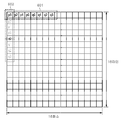
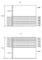
일련의 동작을 설명하기 위해서, 도 13 및 도 14a 및 도 14b를 참조하여, 벡터 검출 회로(802)가 처리한 화상 데이터 영역에 대해서 설명한다. 도 14a 및 도 14b는, 도 3a 및 도 3b와 같이, 마스터측 화상 프로세서(100)와 슬레이브측 화상 프로세서(117)와의 사이에서 화상 데이터의 통신을 행하지 않을 경우에 필요한 데이터량을 나타낸다. 도 14a는, 마스터측 화상 프로세서(100)로 처리되는 상반부의 화상 데이터를 나타내고, 도 14b는, 슬레이브측 화상 프로세서(117)로 처리되는 하반부의 화상 데이터를 나타낸다. 도 14a에 있어서, VIN_M은 마스터측 화상 프로세서(100)의 화상처리 회로(102)에 입력되는 화상 데이터의 라인수를, 영역1407로 나타낸 VOUT_M은 화상 데이터의 출력 라인수를 나타낸다. 더욱, VADD1_M은, 센서 보정회로(201)에 의해 실시된 처리에 사용된 후 삭제되는 화상 데이터 영역의 상단의 라인수를 나타낸다. 마찬가지로, VADD2_M은 광학보정회로(202), VADD3_M은 현상 처리 회로(203), VADD4_M은 NR처리 회로(204)의 처리에 사용된 후 삭제되는 화상 데이터 영역(1401∼1404)의 상단의 라인수를 나타낸다. 추가로, VADD5_M은 축소 처리 회로(801), VADD6_M은 벡터 검출 회로(802)의 처리에 사용된 후 삭제되는 화상 데이터 영역(1405∼1406)의 상단의 라인수를 나타낸다.
To describe a series of operations, the image data area processed by the
마찬가지로, 도 14b에 있어서, VIN_S는 슬레이브측 화상 프로세서(117)의 화상처리 회로(102)에 입력된 화상 데이터의 라인수를, 영역1417로 나타낸 VOUT_S는 화상 데이터의 출력 라인수를 나타낸다. 더욱, VADD1_S는, 센서 보정회로(201)에 의해 실시된 처리에 사용된 후 삭제되는 화상 데이터 영역의 하단의 라인수를 나타낸다. 마찬가지로, VADD2_S는 광학보정회로(202), VADD3_S는 현상 처리 회로(203), VADD4_S는 NR처리 회로(204)의 처리에 사용된 후 삭제되는 화상 데이터 영역(1411∼1414)의 하단의 라인수를 나타낸다. VADD5_S는 축소 처리 회로(801), VADD6_S는 벡터 검출 회로(802)의 처리에 사용된 후 삭제되는 화상 데이터 영역(1415∼1416)의 하단의 라인수를 나타낸다.
Similarly, in Fig. 14B, VIN_S indicates the number of lines of the image data input to the
이하에 촬상 소자로부터의 아날로그 신호를 AD변환기에서 디지털 신호로 변환해서 출력한 화상 데이터가, 3840개의 수평화소와 2160개의 수직 화소일 경우를 일례로서 설명한다. 마스터측 화상 프로세서(100)의 AD변환기로부터 출력된 화상 데이터의 상반부의 데이터는, 마스터측 화상 프로세서(100)의 화상처리 회로(102)에 전송된다. 한편, 화상 데이터의 하반부의 데이터는, 각 프로세서의 통신 회로(104)를 거쳐 슬레이브측 화상 프로세서(117)에 전송된다.
Hereinafter, the case where image data obtained by converting an analog signal from an image pickup device into an analog signal from an A / D converter and output is 3840 horizontal pixels and 2160 vertical pixels will be described as an example. The upper half data of the image data output from the AD converter of the master
그렇지만, 본 실시예에서는, 마스터측 화상 프로세서(100)와 슬레이브측 화상 프로세서(117)와의 사이에서 화상 데이터를 통신한다. 별도로 후술하는 것 같이, 통신 데이터 제어 회로(115)는, 화상 데이터의 상측의 어느 영역을 마스터측 화상 프로세서(100)로 처리하고, 하측의 어느 영역까지 슬레이브측 화상 프로세서(117)에 전송할지를 판정한다. 통신 데이터 제어 회로(115)에 의해 행해진 처리에 관한 상세는 후술한다.
However, in the present embodiment, image data is communicated between the master
본 실시예에서는, 예를 들면 3840개의 수평화소와 2160개의 수직 화소의 화상 데이터에 대하여, 축소 처리 회로(801)가 수평 및 수직방향으로 1/2만큼 화소를 축소하는 축소 처리를 행한다. 통신 데이터 제어 회로(115)에 의해 이루어진 판정에 의해, 수평방향으로 정확히 절반에 해당한 위치에서 화상 프로세서들에 데이터가 전송되게 되는 경우에, 축소 처리 회로(801)는, 도 13에 나타낸 것처럼, 1920개의 수평화소와 540개의 수직화소의 화상 데이터를 출력한다.
In this embodiment, for example, the
상술한 벡터 검출 처리와 같이, 이전 프레임에서 취득한 특징점을 중심으로 이전 프레임의 2값 화상 데이터로부터 템플릿 영역 화상 데이터를 판독하고, 현 프레임의 2값 화상 데이터로부터 서치 영역 화상 데이터를 판독하고, 템플릿 매칭을 실시한다. 또한, 템플릿 영역 화상 데이터는, 예를 들면 48개의 수평화소와 48개의 수직화소인 반면에, 서치 영역 화상 데이터는, 예를 들면 96개의 수평화소와 96개의 수직화소다. The template area image data is read from the binary image data of the previous frame centering on the minutiae acquired in the previous frame as in the above-described vector detection process, the search area image data is read out from the binary image data of the current frame, . The template area image data is, for example, 48 horizontal pixels and 48 vertical pixels, while the search area image data is, for example, 96 horizontal pixels and 96 vertical pixels.
도 13에 나타낸 점선보다 위의 540개의 화소의 데이터는, 마스터측 화상 프로세서(100)내에서 처리된 데이터다. 그러나, 예를 들면, 그리드(1351)로부터 알 수 있듯이, 마스터측 화상 프로세서(100)에서 보유되지 않은 영역으로부터의 데이터가 필요하다. 다시 말해, 특징점(1331)이 그리드(1351)의 하단 근처에 존재하기 때문에, 템플릿 영역(1301)과 서치 영역(1311)의 하단의 사선영역(1321)(예를 들면 96개의 수평화소와 32개의 수직화소)은 마스터측 화상 프로세서(100)의 처리 대상이 아니다. 마찬가지로, 그리드(1353)에서는, 특징점(1333)이 그 그리드의 하단근처에 존재하기 때문에, 템플릿 영역(1303)과 서치 영역(1313)의 하단의 사선영역(1323)(96개의 수평화소와 42개의 수직화소)은 마스터측 화상 프로세서(100)의 처리 대상이 아니다.
The data of 540 pixels above the dotted line shown in Fig. 13 is the data processed in the master
반대로, 도 13에 나타낸 점선보다 아래의 540개의 화소의 데이터는, 슬레이브측 화상 프로세서(117)내에서 처리된 데이터다. 그렇지만, 예를 들면 그리드(1352)로부터 알 수 있듯이, 슬레이브측 화상 프로세서(117)에서 보유되지 않은 영역으로부터의 데이터가 필요하다. 다시 말해, 그리드(1352)의 특징점(1332)이 그리드의 상단근처에 존재하기 때문에, 템플릿 영역(1302)과 서치 영역(1312)의 상단의 사선영역(1322)(96개의 수평화소와 38개의 수직화소)은 슬레이브측 화상 프로세서(117)의 처리 대상이 아니다. 마찬가지로, 그리드(1354)에서는, 특징점(1334)이 그리드의 상단근처에 존재하기 때문에, 템플릿 영역(1304)과 서치 영역(1314)(96개의 수평화소와 32개의 수직화소)의 상단의 사선영역(1324)은 슬레이브측 화상 프로세서(117)의 처리 대상이 아니다.
Conversely, the data of 540 pixels below the dotted line shown in Fig. 13 is the data processed in the slave-
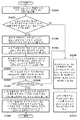
다음에, 도 12를 참조하여, 도 13에 나타낸 상황하에서 실시된, 화상 데이터의 경계영역에 관한 벡터 검출 처리 및 프로세서간의 데이터 통신처리에 대해서 설명한다. 또한, 이후 설명된 일련의 동작은, 시스템 제어회로(114)에 의해 불휘발성 메모리(113)에 기억된 프로그램을 로딩 및 실행하고, 상기 프로세서들을 구성하는 각 회로 혹은 통신 데이터 제어 회로(115)를 제어함으로써 실시된다.
Next, with reference to Fig. 12, the vector detection processing and the inter-processor data communication processing relating to the boundary area of the image data, performed under the situation shown in Fig. 13, will be described. The series of operations to be described below are executed by loading and executing the program stored in the
S1200에 있어서, 통신 데이터 제어 회로(115)는, 벡터 검출 회로(802)의 특징점 산출 회로(902)에서 산출된, 직전의 프레임에서의 특징점 좌표를 사용하여, 템플릿 영역 화상 데이터와 서치 영역 화상 데이터를 산출한다. 도 13에 나타낸 예에서는, 예를 들면 특징점(1331)에 대하여, 서치 영역(1311)과 템플릿 영역(1301)을 산출한다.
In S1200, the communication
S1201에 있어서, 통신 데이터 제어 회로(115)는, 상/하 분할에 의해 얻어진 화상 데이터의 상측에 포함된 그리드의 템플릿 영역 화상 데이터와 서치 영역 화상 데이터가, 하측의 화상 데이터의 영역에 존재하는지를 판정한다. 도 13에 나타낸 예에서는, 통신 데이터 제어 회로(115)는, 템플릿 영역 화상 데이터(1301, 1303)와 서치 영역 화상 데이터(1311, 1313)의 사선영역(1321, 1323)이 하측의 화상 데이터의 영역에 존재한다고 판정한다. 마찬가지로, 통신 데이터 제어 회로(115)는, 상/하 분할에 의해 얻어진 화상 데이터의 하측에 포함된 그리드의 템플릿 영역 화상 데이터와 서치 영역 화상 데이터가, 상측의 화상 데이터의 영역에 존재하는지를 판정한다. 도 13에 나타낸 예에서는, 통신 데이터 제어 회로(115)는, 템플릿 영역 화상 데이터(1302, 1304)와 서치 영역 화상 데이터(1312, 1314)의 사선영역(1322, 1324)이 상측의 화상 데이터의 영역에 존재한다고 판정한다. 통신 데이터 제어 회로(115)는, 템플릿 영역 화상 데이터 또는 서치 영역 화상 데이터가 반대측의 화상 데이터의 영역에 존재한다고 판정했을 경우, S1202에 처리를 진행시킨다. 그렇지 않을 경우에는 S1209에 처리를 진행시킨다.
In S1201, the communication
S1202에 있어서, 통신 데이터 제어 회로(115)는, 입력 화상 데이터의 비트 심도인 bitA와, 템플릿 영역 화상 데이터와 서치 영역 화상 데이터의 비트 심도인 bitB를 판정한다. 전술한 대로, bitA=14비트, bitB=1비트가 된다. S1203에 있어서, 통신 데이터 제어 회로(115)는, 입력 화상 데이터의 화상해상도인 sizeA와 템플릿 영역 화상 데이터 및 서치 영역 화상 데이터의 화상해상도인 sizeB를 판정한다. 전술한 대로, 축소 처리 회로(801)에 의해, 입력 화상 데이터를 1/2배에 축소하고, 2값 데이터의 화상 사이즈에서 화소수를 산출한다. 이 때문에, sizeA=2, sizeB=1이 된다.
In S1202, the communication
S1204에 있어서, 통신 데이터 제어 회로(115)는, 상/하 분할한 경계를 넘는 템플릿 영역 화상 데이터와 서치 영역 화상 데이터를 포함하는 화상 데이터를 센서 보정회로(201)로부터 입력해서 처리할 때에 필요한 라인의 화소수 pixnumA를 산출한다. 여기에서, 마스터측 화상 프로세서(100)의 화소수를 PixnumA_M, 슬레이브측 화상 프로세서(117)의 화소수를 PixnumA_S라고 한다. 도 13에 나타낸 예에서, 이것은, 사선영역(1321 및 1323)을 포함하는 분할 경계로부터 라인 단위의 화소수다. 다시 말해, 이것은, 수직방향의 화소수가 큰 사선영역(1323)의 42화소이기 때문에, 마스터측 화상 프로세서(100)의 화소수 PixnumA_M은 1920×42, 즉 80640화소다. 마찬가지로, PixnumA_S는, 사선영역(1322, 1324)을 포함하는 라인 단위의 화소수다. 다시 말해, 이것은, 수직방향의 화소수가 큰 사선영역(1322)의 38화소이기 때문에, 슬레이브측 화상 프로세서(117)의 화소수 PixnumA_S는 1920×38, 즉 72960화소다.
In S1204, the communication
다음에, 템플릿 영역 화소 데이터와 서치 영역 화소 데이터의 화소수pixnumB을 산출한다. 여기에서, 마스터측 화상 프로세서(100)의 화소수를 PixnumB_M, 슬레이브측 화상 프로세서(117)의 화소수를 PixnumB_S라고 한다. 도 13에 있어서, 사선영역1321(96개의 수평화소와 32개의 수직화소)과, 사선영역1323(96개의 수평화소와 42개의 수직화소)의 템플릿 영역 화상 데이터와 서치 영역 화상 데이터의 화소수가, PixnumB_M이 된다. 따라서, PixnumB_M은, 96×32+48×8+96×42+48×18, 즉 8352화소가 된다. 마찬가지로, 사선영역1322(96개의 수평화소와 38개의 수직화소)과, 사선영역1324(96개의 수평화소와 32개의 수직화소)의 템플릿 영역 화상 데이터와 서치 영역 화상 데이터의 화소수가, PixnumB_S가 된다. 따라서, PixnumB_S는, 96×38+48×10+96×32+48×16, 즉 7968화소가 된다.
Next, the number of pixels pixnumB of the template area pixel data and the search area pixel data is calculated. Here, the number of pixels of the master
S1205에 있어서, 통신 데이터 제어 회로(115)는, 처리에 필요한 라인의 처리 데이터량 datasizeA와 템플릿 영역 화상 데이터와 서치 영역 화상 데이터의 처리 데이터량 datasizeB를 산출한다. 구체적으로는, 통신 데이터 제어 회로(115)는, datasizeA와 datasizeB를, S1202∼1204에 있어서 얻어진 비트 심도, 화상해상도, 화소수를 고려해서 산출한다. 또한, 마스터측 화상 프로세서(100)의 처리 데이터량을 datasizeA_M, datasizeB_M로 하는 한편, 슬레이브측 화상 프로세서(117)의 처리 데이터량을 datasizeA_S, datasizeB_S로 한다.
In S1205, the communication
도 13에 나타낸 예에서는, 마스터측 화상 프로세서(100)의 처리 데이터량은,
In the example shown in Fig. 13, the processing data amount of the master
·datasizeA_M=bitA×sizeA^2×PixnumA_M=14×2^2×80640=4515840(bits)? DatasizeA_M = bitA x size? 2 x PixnumA_M = 14 x 2 ^ 2 x 80640 = 4515840 (bits)
·datasizeB_M=bitB×sizeB^2×PixnumB_M=1×1^2×8352=8352(bits)다.? DatasizeB_M = bitB 占 sizeB? 2 占 PixnumB_M = 1 占 2 占 8352 = 8352 (bits).
한편, 슬레이브측 화상 프로세서(117)의 처리 데이터량은,
On the other hand, the processing data amount of the slave
·datasizeA_S=bitA×sizeA^2×PixnumA_S=14×2^2×72960=4085760(bits)다.? DatasizeA_S = bitA × sizeA ^ 2 × PixnumA_S = 14 × 2 ^ 2 × 72960 = 4085760 (bits).
·datasizeB_S=bitB×sizeB^2×Pixnum _S=1×1^2×7968=7968(bits)다.Bit size B ^ 2 x Pixnum_S = 1 x 1 ^ 2 x 7968 = 7968 (bits).
따라서, 이것들을 합산한 처리 데이터량은, datasizeA=datasizeA_M+datasizeA_S=8601600(bits), datasizeB=datasize B_M+datasizeB_S=16320(bits)다. Therefore, the amount of processed data obtained by summing them is as follows: datasizeA = datasizeA_M + datasizeA_S = 8601600 (bits), datasizeB = datasize B_M + datasizeB_S = 16320 (bits).
S1206에 있어서, 통신 데이터 제어 회로(115)는, S1205에서 산출한 처리 데이터량을 비교한다. 통신 데이터 제어 회로(115)는, datasizeA <datasizeB인 경우, 즉 datasizeA가 datasizeB를 하회하는 경우, S1207에 처리를 진행시킨다. 그렇지 않은 경우에는, S1209에 처리를 진행시킨다. 도 13에 나타낸 예에서는, 통신 데이터 제어 회로(115)는 이 조건을 충족시키지 않는다고 판정하고, S1209에 처리를 진행시킨다.
In S1206, the communication
S1207에 있어서, 마스터측 화상 프로세서(100)의 통신 회로(104)는, (시스템 제어 회로(114)의 지시에 응답하여) 입력 화상 데이터 중, 상/하 분할된 하반부의 화상 데이터를 슬레이브측 화상 프로세서(117)에 전송한다. 아울러, 입력 화상 데이터 중, 상/하 분할된 상반부의 화상 데이터에서 템플릿 영역 화상 데이터 및 서치 영역 화상 데이터를 포함하는 라인 단위의 화상 데이터를 슬레이브측 화상 프로세서(117)에 전송한다. 도 13에 나타낸 예에서는, 사선영역(1322)을 포함하는 38화소 라인과 하반부의 화상 데이터의 540화소 라인을 슬레이브측 화상 프로세서(117)에 전송한다.
In S1207, the
S1208에 있어서, 마스터측 화상 프로세서(100) 또는 슬레이브측 화상 프로세서(117)는, 상/하 분할에 의해 얻어진 절반의 화상 데이터와, 템플릿 영역 화상 데이터 및 서치 영역 화상 데이터를 포함하는 라인들의 화상 데이터를, 화상처리 회로(102)내의 화상처리 모듈로 순차로 처리한다. 다시 말해, 마스터측 화상 프로세서(100)는, 상/하 분할에 의해 얻어진 상반부의 화상 데이터와, 템플릿 영역 화상 데이터 및 서치 영역 화상 데이터를 포함하는 라인들의 화상 데이터를, 순차로 처리한다. 예를 들면, 축소 처리 회로(801)는, 도 14a에 나타낸 VOUT_M=540과 VADD6_M=42를 포함하는 라인분의 출력 화상 데이터를 처리하고 나서, 이 처리후의 데이터를 벡터 검출 회로(802)가 처리한다. 한편, 슬레이브측 화상 프로세서(117)는, 상/하 분할에 의해 얻어진 하반부의 화상 데이터와, 템플릿 영역 화상 데이터 및 서치 영역 화상 데이터를 포함하는 라인들의 화상 데이터를 순차로 처리한다. 축소 처리 회로(801)는, 도 14b에 나타낸 VOUT_S=540과 VADD6_S=38을 포함하는 라인 분의 화상 데이터를 처리하고 나서, 이 처리후의 데이터를 벡터 검출 회로(802)가 처리한다.
In S1208, the master-
S1209에 있어서, 마스터측 화상 프로세서(100)의 통신 회로(104)는, 슬레이브측 화상 프로세서(117)의 벡터 검출 회로(802)에서 필요한 템플릿 영역 화상 데이터 및 서치 영역 화상 데이터를 슬레이브측 화상 프로세서(117)에 전송한다. 마찬가지로, 슬레이브측 화상 프로세서(117)의 통신 회로(104)는, 마스터측 화상 프로세서(100)의 벡터 검출 회로(802)에서 필요한 템플릿 영역 화상 데이터 및 서치 영역 화상 데이터를 마스터측 화상 프로세서(100)에 전송한다. 도 13에 나타낸 예에서는, 마스터측 화상 프로세서(100)의 통신 데이터 제어 회로(115)는, 벡터 검출 회로(802)에서 처리된 2값 데이터 중, 사선영역(1322 및 1324)의 화상 데이터를 슬레이브측 화상 프로세서(117)에 전송한다.
한편, 슬레이브측 화상 프로세서(117)의 통신 데이터 제어 회로(115)는, 벡터 검출 회로(802)에서 처리된 2값 데이터 중, 사선영역(1321 및 1323)의 화상 데이터를 마스터측 화상 프로세서(100)에 전송한다.
The
S1210에 있어서, 마스터측 화상 프로세서(100)에서는, 상/하 분할에 의해 얻어진 상반부의 화상 데이터를 화상처리 회로(102)내의 각 블록에서 순차로 처리한다. 예를 들면, 축소 처리 회로(801)는, 도 14a에 나타낸 VOUT_M=540의 라인분의 화상 데이터를 처리하고 나서, 이 처리후의 데이터를 벡터 검출 회로(802)가 처리한다. 벡터 검출 회로(802)는, (벡터 검출 처리에 필요한) 상/하 분할에 의해 얻어진 하반부의 화상 데이터에 포함된 템플릿 영역 화상 데이터와 서치 영역 화상 데이터는, 슬레이브측 화상 프로세서(117)로부터 전송된 데이터를 사용한다.
In S1210, the master
한편, 슬레이브측 화상 프로세서(117)에서는, 상/하 분할에 의해 얻어진 하반부의 화상 데이터를 화상처리 회로(102)내의 각 블록에서 순차로 처리한다. 예를 들면, 축소 처리 회로(801)는, 도 14b에 나타낸 VOUT_S=540의 라인분의 화상 데이터를 처리하고 나서, 이 처리후의 데이터를 벡터 검출 회로(802)가 처리한다. 벡터 검출 회로(802)에서는, (벡터 검출 처리에 필요한) 상/하 분할에 의해 얻어진 상반부의 화상 데이터에 포함된 템플릿 영역 화상 데이터와 서치 영역 화상 데이터는, 마스터측 화상 프로세서(100)로부터 전송된 데이터를 사용한다.
On the other hand, in the slave
통신 데이터 제어 회로(115)는, S1208 또는 S1210의 처리를 완료하면, 본 일련의 동작을 종료한다. 또한, 도 12에 나타낸 일련의 동작은, 1프레임마다 또는 몇몇의 프레임마다 실시되어도 좋다. 추가로, 그 동작은, 동화상의 촬영시와 아울러, 동화상을 재생할 경우에 적용되어도 좋다. 더욱, 동화상을 재생할 경우에는, 예를 들면 S1205까지의 처리를 미리 실행해두고, 산출한 데이터를 기억해도 좋다. 상술한 실시예에서는, 2개의 화상 프로세서간에 실시된 처리에 대해서 설명했지만, 그 실시예는 3개 이상의 화상 프로세서간에 실시된 처리에서도 적용될 수 있다. 또한, 상술한 실시예에서는, 화상을 상하부분으로 일례로서 분할하는 경우를 설명했지만, 그 실시예는 화상을 좌우부분, 3개 이상의 부분 등으로 분할하는 경우에도 적용될 수 있다.
The communication
이상 설명한 바와 같이, 본 실시예에서는, 벡터 검출 회로(802)에 있어서 추가적으로 필요한 데이터량이 프레임마다 산출가능하고, 그 추가의 필요한 데이터를 라인 단위로 취득할 경우보다도 데이터량이 적을 경우, 프레임마다 전송이 실시된다. 이렇게 하면, (화상처리 회로(102)의) 처리의 전단에 사용된 블록에서 처리되는 화상 데이터량을 삭감할 수 있고, 전송된 데이터량을 삭감할 수 있고, 처리 전체에 요하는 시간을 단축할 수 있으며, 소비된 전력의 양을 감소할 수 있다.
As described above, in the present embodiment, the amount of data additionally required in the
그 밖의 실시예 Other Embodiments
또한, 본 발명의 실시예들은, 기억매체(보다 완전하게는 '비일시적 컴퓨터 판독 가능한 기억매체'라고도 함)에 레코딩된 컴퓨터 실행가능한 명령어들(예를 들면, 하나 이상의 프로그램)을 판독하고 실행하여 상술한 실시예들의 하나 이상의 기능을 수행하는 것 및/또는 상술한 실시예들의 하나 이상의 기능을 수행하기 위한 하나 이상의 회로(예를 들면, 주문형 반도체(ASIC))를 구비하는 것인, 시스템 또는 장치를 갖는 컴퓨터에 의해 실현되고, 또 예를 들면 상기 기억매체로부터 상기 컴퓨터 실행가능한 명령어를 판독하고 실행하여 상기 실시예들의 하나 이상의 기능을 수행하는 것 및/또는 상술한 실시예들의 하나 이상의 기능을 수행하는 상기 하나 이상의 회로를 제어하는 것에 의해 상기 시스템 또는 상기 장치를 갖는 상기 컴퓨터에 의해 행해지는 방법에 의해 실현될 수 있다. 상기 컴퓨터는, 하나 이상의 프로세서(예를 들면, 중앙처리장치(CPU), 마이크로처리장치(MPU))를 구비하여도 되고, 컴퓨터 실행 가능한 명령어를 판독하여 실행하기 위해 별개의 컴퓨터나 별개의 프로세서의 네트워크를 구비하여도 된다. 상기 컴퓨터 실행가능한 명령어를, 예를 들면 네트워크나 상기 기억매체로부터 상기 컴퓨터에 제공하여도 된다. 상기 기억매체는, 예를 들면, 하드 디스크, 랜덤액세스 메모리(RAM), 판독전용 메모리(ROM), 분산형 컴퓨팅 시스템의 스토리지, 광디스크(콤팩트 디스크(CD), 디지털 다기능 디스크(DVD) 또는 블루레이 디스크(BD)TM등), 플래시 메모리 소자, 메모리 카드 등 중 하나 이상을 구비하여도 된다.Embodiments of the present invention may also be practiced with computer-readable instructions (e.g., one or more programs) recorded on a storage medium (more fully, " non-volatile computer readable storage medium & (E.g., an application specific integrated circuit (ASIC)) for performing one or more functions of the above-described embodiments and / or performing one or more functions of the embodiments described above. For example, by reading and executing the computer-executable instructions from the storage medium to perform one or more functions of the embodiments and / or perform one or more functions of the embodiments described above By said computer having said system or said device by controlling said at least one circuit It can be realized by the method. The computer may comprise one or more processors (e.g., a central processing unit (CPU), a microprocessor unit (MPU)) or may be a separate computer or a separate processor for reading and executing computer- A network may be provided. The computer-executable instructions may be provided to the computer from, for example, a network or the storage medium. The storage medium may be, for example, a hard disk, a random access memory (RAM), a read only memory (ROM), a storage of a distributed computing system, an optical disk (compact disk (CD), digital versatile disk Disk (BD) TM, etc.), a flash memory device, a memory card, and the like.
본 발명을 실시예들을 참조하여 설명하였지만, 본 발명은 상기 개시된 실시예들에 한정되지 않는다는 것을 알 것이다. 아래의 청구항의 범위는, 모든 변형예, 동등한 구조 및 기능을 포함하도록 폭 넓게 해석해야 한다. While the present invention has been described with reference to exemplary embodiments, it is to be understood that the invention is not limited to the disclosed exemplary embodiments. The scope of the following claims is to be accorded the broadest interpretation so as to encompass all modifications, equivalent structures and functions.
Claims (17)
상기 화상을 형성하는 상기 화상신호로부터 취득된 제2의 화상신호에 상기 화상 처리를 실시하는 제2의 처리 회로; 및
상기 제1의 처리 회로와 상기 제2의 처리 회로에서 실시된 상기 화상처리의 진행에 따라, 상기 제1의 처리 회로와 상기 제2의 처리 회로간의 화상신호의 통신을 제어하는 제어 회로를 구비하고,
상기 제1의 화상신호와 상기 제2의 화상신호는, 상기 화상의 영역이 중복하지 않도록 상기 화상을 영역들로 분할하여서 얻어진 화상신호이며,
상기 제어 회로는, 상기 제1의 처리 회로가 상기 제1의 화상신호에 상기 화상 처리를 실시할 때에 추가적으로 필요한 상기 화상의 영역의 화상신호를, 상기 제2의 처리 회로로부터 상기 제1의 처리 회로에 전송하도록 상기 통신을 제어하는, 화상처리장치.
A first processing circuit for performing image processing on a first image signal acquired from an image signal forming one image;
A second processing circuit for performing the image processing on a second image signal acquired from the image signal forming the image; And
And a control circuit for controlling communication of an image signal between the first processing circuit and the second processing circuit in accordance with progress of the image processing performed in the first processing circuit and the second processing circuit ,
Wherein the first image signal and the second image signal are image signals obtained by dividing the image into regions so that the region of the image does not overlap,
Wherein the control circuit controls the first processing circuit to output an image signal of an area of the image that is additionally required when the first processing circuit performs the image processing on the first image signal, To the image processing apparatus.
상기 화상처리는, 순서대로 실시된 제1의 화상처리와 제2의 화상처리를 포함하고,
상기 제어 회로는, 상기 제1의 처리 회로가 상기 제2의 화상 처리를 행할 때에 추가적으로 필요한 상기 화상의 영역의 화상신호를, 상기 제2의 처리 회로가 상기 제1의 화상 처리를 실시한 후의 화상신호로부터 전송하도록 상기 통신을 제어하는, 화상처리장치.
The method according to claim 1,
Wherein the image processing includes first image processing and second image processing performed in order,
Wherein the control circuit controls the image signal of the area of the image which is additionally required when the first processing circuit performs the second image processing so that the image signal of the image signal after the first processing circuit performs the first image processing And controls the communication to transmit the image data.
상기 추가적으로 필요한 상기 화상의 영역의 화상신호는, 상기 제1의 처리 회로가 상기 화상 처리를 실시하는 화상신호에 포함되지 않는, 상기 화상을 영역들로 분할한 경계로부터 소정의 범위내에 있는 영역의 화상신호인, 화상처리장치.
3. The method of claim 2,
The image signal of the region of the image which is additionally required is the image of the region within the predetermined range from the boundary where the first processing circuit is not included in the image signal subjected to the image processing, Image processing apparatus.
상기 제어 회로는, 상기 추가적으로 필요한 상기 화상의 영역의 화상신호를, 상기 경계로부터 라인 단위로 취득해서 전송하도록 상기 통신을 제어하는, 화상처리장치.
The method of claim 3,
Wherein the control circuit controls the communication so as to acquire the image signal of the region of the image that is additionally required from the boundary line by line.
상기 제2의 화상처리는 움직임 벡터를 검출하는 처리이며,
상기 제어 회로는, 상기 추가적으로 필요한 상기 화상의 영역의 화상신호를, 상기 움직임 벡터를 탐색하기 위해서 필요한 프레임의 영역 중, 상기 경계를 넘는 영역마다 취득해서 전송하도록, 상기 통신을 제어하는, 화상처리장치.
The method of claim 3,
The second image processing is processing for detecting a motion vector,
Wherein the control circuit controls the communication so as to acquire and transmit the image signal of the region of the image further required for each of the regions of the frame necessary for searching for the motion vector, .
상기 제어 회로는, 상기 추가적으로 필요한 상기 화상의 영역의 화상신호에 대해서, 상기 화상 처리를 실시하기 위해서 필요한 프레임의 영역 중, 상기 경계를 넘는 영역마다 취득된 화상신호의 데이터량이, 상기 경계로부터 소정의 라인수에서 취득된 화상신호의 데이터량을 하회하는지를 판정하는, 화상처리장치.
The method of claim 3,
The control circuit controls the control circuit so that the data amount of the image signal acquired for each of the regions exceeding the border among the regions of the frame necessary for performing the image processing on the image signal of the region of the image further required, And determines whether the amount of data of the image signal obtained in the number of lines is lower than the amount of data of the image signal acquired in the number of lines.
상기 제어 회로는, 상기 경계를 넘는 영역마다 취득된 화상신호의 데이터량이, 상기 경계로부터 상기 소정의 라인수에서 취득된 화상신호의 데이터량을 하회한다고 판정했을 경우, 상기 경계를 넘는 영역마다 취득된 화상신호를 취득해서 전송하도록 상기 통신을 제어하는, 화상처리장치.
The method according to claim 6,
When it is judged that the data amount of the image signal acquired for each of the regions crossing the border is lower than the data amount of the image signal acquired from the predetermined number of lines from the border, And controls the communication to acquire and transmit an image signal.
상기 제어 회로는, 데이터량을 판정할 때에, 상기 제2의 처리 회로에 의해 실시된 화상처리에 의해 취득된 화상신호의 비트 심도를 고려하는, 화상처리장치.
The method according to claim 6,
Wherein the control circuit considers the bit depth of the image signal obtained by the image processing performed by the second processing circuit when determining the amount of data.
상기 제어 회로는, 데이터량을 판정할 때에, 상기 제2의 처리 회로에 의해 실시된 화상처리에 의해 취득된 화상신호의 해상도를 고려하는, 화상처리장치.
The method according to claim 6,
Wherein the control circuit considers the resolution of the image signal obtained by the image processing performed by the second processing circuit when determining the amount of data.
상기 화상처리는, 순서대로 실시된 제1의 화상처리와 제2의 화상처리를 구비하고,
상기 제어 회로는, 상기 제1의 처리 회로가 상기 제1의 화상 처리를 실시할 때에, 상기 제2의 처리 회로로부터 상기 제1의 처리 회로에 전송된 상기 화상의 영역과, 상기 제1의 처리 회로가 상기 제2의 화상 처리를 실시할 때에, 상기 제2의 처리 회로로부터 상기 제1의 처리 회로에 전송된 상기 화상의 영역을, 개별적으로 설정하는, 화상처리장치.
The method according to claim 1,
The image processing includes first image processing and second image processing performed in order,
Wherein the control circuit is configured to control the area of the image transferred from the second processing circuit to the first processing circuit when the first processing circuit performs the first image processing, And sets an area of the image transferred from the second processing circuit to the first processing circuit individually when the circuit performs the second image processing.
상기 제어 회로는, 상기 제1의 화상처리에 근거하여, 상기 제1의 처리 회로가 상기 제1의 화상 처리를 실시할 때에, 상기 제2의 처리 회로로부터 상기 제1의 처리 회로에 전송된 상기 화상의 영역을 설정하고, 상기 제2의 화상처리에 근거하여, 상기 제1의 처리 회로가 상기 제2의 화상 처리를 실시할 때에, 상기 제2의 처리 회로로부터 상기 제1의 처리 회로에 전송된 상기 화상의 영역을 설정하는, 화상처리장치.
11. The method of claim 10,
Wherein the control circuit controls the first processing circuit to perform the first image processing on the basis of the first image processing when the first processing circuit performs the first image processing, Wherein the first processing circuit sets an area of an image and transfers the second processing circuit from the second processing circuit to the first processing circuit when the first processing circuit performs the second image processing based on the second image processing And sets the area of the image that has been captured.
상기 제어 회로는, 상기 제2의 처리 회로에, 상기 제1의 처리 회로가 상기 제1의 화상신호에 상기 화상 처리를 실시할 때에 추가적으로 필요한 상기 화상의 영역의 화상신호의 데이터량을 삭감시키고, 데이터량이 삭감된 상기 화상의 영역의 화상신호는 상기 제2의 처리 회로로부터 상기 제1의 처리 회로에 전송되는, 화상처리장치.
The method according to claim 1,
The control circuit may cause the second processing circuit to reduce the data amount of the image signal of the area of the image which is additionally required when the first processing circuit performs the image processing on the first image signal, The image signal of the area of the image whose data amount is reduced is transferred from the second processing circuit to the first processing circuit.
상기 제1의 처리 회로는, 상기 제1의 화상신호의 데이터량을 삭감하고, 데이터량을 삭감한 상기 제1의 화상신호와, 상기 제어 회로에 의해 전송된 상기 데이터량이 삭감된 상기 화상의 영역의 화상신호를 사용하여, 상기 화상 처리를 실시하는, 화상처리장치.
13. The method of claim 12,
Wherein the first processing circuit is configured to reduce the amount of data of the first image signal and reduce the amount of data of the first image signal that is obtained by reducing the amount of data, And the image processing unit performs the image processing using the image signal of the image processing unit.
상기 제1의 처리 회로와 상기 제2의 처리 회로는, 서로 다른 화상 프로세서인, 화상처리장치.
The method according to claim 1,
Wherein the first processing circuit and the second processing circuit are different image processors.
상기 제어 회로는, 복수의 화상 프로세서 중 하나에 의해 실현되는, 화상처리장치.
15. The method of claim 14,
Wherein the control circuit is realized by one of a plurality of image processors.
상기 제1의 처리 회로에 의해, 1개의 화상을 형성하는 화상신호로부터 취득된 제1의 화상신호에 화상 처리를 실시하는 단계;
상기 제2의 처리 회로에 의해, 상기 화상을 형성하는 상기 화상신호로부터 취득된 제2의 화상신호에 상기 화상 처리를 실시하는 단계; 및
상기 프로세서에 의해, 상기 제1의 처리 회로와 상기 제2의 처리 회로에서 실시된 상기 화상처리의 진행에 따라, 상기 제1의 처리 회로와 상기 제2의 처리 회로간의 화상신호의 통신을 제어하는 단계를 포함하고,
상기 제1의 화상신호와 상기 제2의 화상신호는, 상기 화상의 영역이 중복하지 않도록 상기 화상을 영역들로 분할하여서 얻어진 화상신호이며,
상기 제어하는 단계에서는, 상기 제1의 처리 회로가 상기 제1의 화상신호에 상기 화상 처리를 실시하는 단계에서 추가적으로 필요한 상기 화상의 영역의 화상신호를, 상기 제2의 처리 회로가 상기 화상 처리를 실시하는 단계에서 취득된 상기 화상 신호로부터 전송하도록, 상기 통신을 제어하는, 화상처리장치의 제어 방법.
A control method for an image processing apparatus comprising a first processing circuit, a second processing circuit, and a processor,
Performing image processing on a first image signal obtained from an image signal forming one image by the first processing circuit;
Performing the image processing on the second image signal acquired from the image signal forming the image by the second processing circuit; And
The processor controls communication of an image signal between the first processing circuit and the second processing circuit in accordance with progress of the image processing performed in the first processing circuit and the second processing circuit ≪ / RTI >
Wherein the first image signal and the second image signal are image signals obtained by dividing the image into regions so that the region of the image does not overlap,
And the second processing circuit performs the image processing on the image signal of the region of the image which is additionally required in the step of performing the image processing on the first image signal, Wherein the control unit controls the communication so as to transmit the image signal obtained from the image signal obtained in the performing step.
상기 제1의 처리 회로에, 1개의 화상을 형성하는 화상신호로부터 취득된 제1의 화상신호에 화상 처리를 실시시키는 코드;
상기 제2의 처리 회로에, 상기 화상을 형성하는 화상신호로부터 취득된 제2의 화상신호에 화상 처리를 실시시키는 코드; 및
상기 프로세서에, 상기 제1의 처리 회로와 상기 제2의 처리 회로에 의해 행해진 상기 화상처리의 진행에 따라, 상기 제1의 처리 회로와 상기 제2의 처리 회로간의 화상신호의 통신의 제어를 실시시키는 코드를 포함하고,
상기 제1의 화상신호와 상기 제2의 화상신호는, 상기 화상의 영역이 중복하지 않도록 상기 화상을 영역들로 분할한 화상신호이며,
상기 프로세서에 실시시키는 상기 코드는, 상기 제1의 처리 회로가 상기 제1의 화상신호에 상기 화상 처리를 실시하는데 추가적으로 필요한 상기 화상의 영역의 화상신호를, 상기 제2의 처리 회로에 상기 화상 처리를 실시시키는 상기 코드에 의해 취득된 상기 화상 신호로부터 전송하도록, 상기 통신을 제어하는, 기억매체.A computer-readable storage medium storing a computer program for causing a computer to function as an image processing apparatus comprising a first processing circuit, a second processing circuit, and a processor,
A code for causing the first processing circuit to perform image processing on a first image signal acquired from an image signal forming one image;
A code for causing the second processing circuit to perform image processing on a second image signal acquired from an image signal forming the image; And
The control of communication of an image signal between the first processing circuit and the second processing circuit is performed in accordance with the progress of the image processing performed by the first processing circuit and the second processing circuit , ≪ / RTI >
The first image signal and the second image signal are image signals obtained by dividing the image into regions so that the region of the image does not overlap,
Wherein the code to be executed by the processor is to cause the first processing circuit to output the image signal of the area of the image which is additionally required to perform the image processing on the first image signal to the second processing circuit From the image signal obtained by the code for causing the computer to perform the processing.
Applications Claiming Priority (2)
| Application Number | Priority Date | Filing Date | Title |
|---|---|---|---|
| JP2016159681A JP6726060B2 (en) | 2016-08-16 | 2016-08-16 | Image processing apparatus, control method thereof, and program |
| JPJP-P-2016-159681 | 2016-08-16 |
Publications (1)
| Publication Number | Publication Date |
|---|---|
| KR20180019483A true KR20180019483A (en) | 2018-02-26 |
Family
ID=61192446
Family Applications (1)
| Application Number | Title | Priority Date | Filing Date |
|---|---|---|---|
| KR1020170100842A KR20180019483A (en) | 2016-08-16 | 2017-08-09 | Image processing apparatus that divides and processes an image signal, control method thereof, and storage medium |
Country Status (4)
| Country | Link |
|---|---|
| US (1) | US10277810B2 (en) |
| JP (1) | JP6726060B2 (en) |
| KR (1) | KR20180019483A (en) |
| CN (1) | CN107770435A (en) |
Families Citing this family (6)
| Publication number | Priority date | Publication date | Assignee | Title |
|---|---|---|---|---|
| DE102016109179B4 (en) * | 2015-05-29 | 2023-08-03 | Canon Kabushiki Kaisha | Image pickup device and imaging device |
| US10257393B2 (en) | 2016-02-12 | 2019-04-09 | Contrast, Inc. | Devices and methods for high dynamic range video |
| US10264196B2 (en) | 2016-02-12 | 2019-04-16 | Contrast, Inc. | Systems and methods for HDR video capture with a mobile device |
| EP3497925B1 (en) | 2016-08-09 | 2022-11-23 | Contrast, Inc. | Real-time hdr video for vehicle control |
| US11423514B2 (en) * | 2018-08-14 | 2022-08-23 | Contrast, Inc. | Image processing noise reduction |
| JP7332399B2 (en) * | 2019-09-06 | 2023-08-23 | キヤノン株式会社 | Image processing device and its control method |
Family Cites Families (5)
| Publication number | Priority date | Publication date | Assignee | Title |
|---|---|---|---|---|
| US7755669B2 (en) * | 2003-11-28 | 2010-07-13 | Canon Kabushiki Kaisha | Image capture apparatus and image capture method in which an image is processed by a plurality of image processing devices |
| US8212831B1 (en) * | 2004-12-15 | 2012-07-03 | Nvidia Corporation | Broadcast aperture remapping for multiple graphics adapters |
| US20070041448A1 (en) * | 2005-08-17 | 2007-02-22 | Miller Casey L | Artifact and noise reduction in MPEG video |
| JP2016010112A (en) | 2014-06-26 | 2016-01-18 | オリンパス株式会社 | Image processing apparatus |
| JP2017204170A (en) | 2016-05-12 | 2017-11-16 | キヤノン株式会社 | Image processing device and image processing method |
-
2016
- 2016-08-16 JP JP2016159681A patent/JP6726060B2/en active Active
-
2017
- 2017-08-09 KR KR1020170100842A patent/KR20180019483A/en unknown
- 2017-08-15 US US15/677,107 patent/US10277810B2/en active Active
- 2017-08-16 CN CN201710703044.4A patent/CN107770435A/en not_active Withdrawn
Also Published As
| Publication number | Publication date |
|---|---|
| US20180054566A1 (en) | 2018-02-22 |
| CN107770435A (en) | 2018-03-06 |
| JP2018029245A (en) | 2018-02-22 |
| JP6726060B2 (en) | 2020-07-22 |
| US10277810B2 (en) | 2019-04-30 |
Similar Documents
| Publication | Publication Date | Title |
|---|---|---|
| KR20180019483A (en) | Image processing apparatus that divides and processes an image signal, control method thereof, and storage medium | |
| JPWO2009037828A1 (en) | Image coding apparatus and image decoding apparatus | |
| US8373775B2 (en) | Apparatus, method and software stored on a computer-readable storage medium, for reducing noise in an image | |
| JP2018032949A (en) | Motion vector detector and control method thereof | |
| US20150062371A1 (en) | Encoding apparatus and method | |
| JP5092536B2 (en) | Image processing apparatus and program thereof | |
| JP7117872B2 (en) | IMAGE PROCESSING DEVICE, IMAGING DEVICE, IMAGE PROCESSING METHOD, AND PROGRAM | |
| US20150234171A1 (en) | Imaging system, imaging apparatus, and image processing apparatus | |
| US11196925B2 (en) | Image processing apparatus that detects motion vectors, method of controlling the same, and storage medium | |
| JP6576179B2 (en) | Image processing apparatus, image processing method, and program | |
| JP2007267123A (en) | Moving image encoding apparatus | |
| JP6090430B2 (en) | Encoding apparatus, method, program, computer system, recording medium | |
| US9392169B2 (en) | Image processing apparatus, image processing method, program, and imaging apparatus | |
| JP2012018621A (en) | Image processing apparatus, image processing method and program | |
| US20210279572A1 (en) | Information processing apparatus, inference apparatus, control methods thereof, and recording medium | |
| JP2020123864A (en) | Image encoder | |
| JP6225137B2 (en) | In-vehicle camera image processing device | |
| JP4720339B2 (en) | Image processing apparatus, image processing program, and electronic camera | |
| US20230057659A1 (en) | Encoder, method, and non-transitory computer-readable storage medium | |
| JP6838951B2 (en) | Coding device and coding method | |
| JP6667349B2 (en) | Image processing device and imaging device | |
| JP6519185B2 (en) | Video encoder | |
| JP2007158524A (en) | Image coding apparatus and method | |
| JP2021103454A (en) | Image processor, method for processing image, learning device, method for learning, program, and system | |
| JP2016066922A (en) | Signal processor, imaging apparatus, and signal processing method in them |