KR20170132745A - Gallium nitride-based sintered compact and method for manufacturing same - Google Patents
Gallium nitride-based sintered compact and method for manufacturing sameInfo
- Publication number
- KR20170132745A KR20170132745A KR1020177026289A KR20177026289A KR20170132745A KR 20170132745 A KR20170132745 A KR 20170132745A KR 1020177026289 A KR1020177026289 A KR 1020177026289A KR 20177026289 A KR20177026289 A KR 20177026289A KR 20170132745 A KR20170132745 A KR 20170132745A
- Authority
- KR
- South Korea
- Prior art keywords
- gallium nitride
- sintered body
- less
- film
- gallium
- Prior art date
Links
- 229910002601 GaN Inorganic materials 0.000 title claims abstract description 106
- JMASRVWKEDWRBT-UHFFFAOYSA-N Gallium nitride Chemical compound [Ga]#N JMASRVWKEDWRBT-UHFFFAOYSA-N 0.000 title claims abstract description 100
- 238000000034 method Methods 0.000 title claims description 50
- 238000004519 manufacturing process Methods 0.000 title claims description 14
- QVGXLLKOCUKJST-UHFFFAOYSA-N atomic oxygen Chemical compound [O] QVGXLLKOCUKJST-UHFFFAOYSA-N 0.000 claims abstract description 48
- 239000001301 oxygen Substances 0.000 claims abstract description 48
- 229910052760 oxygen Inorganic materials 0.000 claims abstract description 48
- 238000005477 sputtering target Methods 0.000 claims abstract description 29
- 239000000843 powder Substances 0.000 claims abstract description 27
- 239000010409 thin film Substances 0.000 claims abstract description 22
- GYHNNYVSQQEPJS-UHFFFAOYSA-N Gallium Chemical compound [Ga] GYHNNYVSQQEPJS-UHFFFAOYSA-N 0.000 claims description 29
- 229910052733 gallium Inorganic materials 0.000 claims description 29
- 239000002245 particle Substances 0.000 claims description 27
- 238000010438 heat treatment Methods 0.000 claims description 18
- 229910052738 indium Inorganic materials 0.000 claims description 10
- APFVFJFRJDLVQX-UHFFFAOYSA-N indium atom Chemical compound [In] APFVFJFRJDLVQX-UHFFFAOYSA-N 0.000 claims description 10
- 239000002994 raw material Substances 0.000 claims description 10
- WFKWXMTUELFFGS-UHFFFAOYSA-N tungsten Chemical compound [W] WFKWXMTUELFFGS-UHFFFAOYSA-N 0.000 claims description 7
- 229910052721 tungsten Inorganic materials 0.000 claims description 7
- 239000010937 tungsten Substances 0.000 claims description 7
- 238000001556 precipitation Methods 0.000 claims description 6
- HCHKCACWOHOZIP-UHFFFAOYSA-N Zinc Chemical compound [Zn] HCHKCACWOHOZIP-UHFFFAOYSA-N 0.000 claims description 4
- 229910052725 zinc Inorganic materials 0.000 claims description 4
- 239000011701 zinc Substances 0.000 claims description 4
- ATJFFYVFTNAWJD-UHFFFAOYSA-N Tin Chemical compound [Sn] ATJFFYVFTNAWJD-UHFFFAOYSA-N 0.000 claims description 3
- 229910052718 tin Inorganic materials 0.000 claims description 3
- 238000007731 hot pressing Methods 0.000 abstract description 4
- 230000000704 physical effect Effects 0.000 abstract description 2
- 239000010408 film Substances 0.000 description 53
- 239000010410 layer Substances 0.000 description 36
- 239000000758 substrate Substances 0.000 description 33
- 239000013078 crystal Substances 0.000 description 32
- 229910052751 metal Inorganic materials 0.000 description 22
- 239000002184 metal Substances 0.000 description 22
- 238000004544 sputter deposition Methods 0.000 description 21
- 239000000463 material Substances 0.000 description 20
- 238000005259 measurement Methods 0.000 description 19
- IJGRMHOSHXDMSA-UHFFFAOYSA-N Atomic nitrogen Chemical compound N#N IJGRMHOSHXDMSA-UHFFFAOYSA-N 0.000 description 16
- 238000005245 sintering Methods 0.000 description 14
- 230000015572 biosynthetic process Effects 0.000 description 13
- 229910000679 solder Inorganic materials 0.000 description 11
- XUIMIQQOPSSXEZ-UHFFFAOYSA-N Silicon Chemical compound [Si] XUIMIQQOPSSXEZ-UHFFFAOYSA-N 0.000 description 9
- 229910052976 metal sulfide Inorganic materials 0.000 description 9
- 239000010703 silicon Substances 0.000 description 9
- 229910052710 silicon Inorganic materials 0.000 description 9
- 238000010304 firing Methods 0.000 description 8
- 239000007789 gas Substances 0.000 description 8
- 229910052757 nitrogen Inorganic materials 0.000 description 8
- 238000012360 testing method Methods 0.000 description 7
- 238000001755 magnetron sputter deposition Methods 0.000 description 6
- CADICXFYUNYKGD-UHFFFAOYSA-N sulfanylidenemanganese Chemical compound [Mn]=S CADICXFYUNYKGD-UHFFFAOYSA-N 0.000 description 6
- 230000000052 comparative effect Effects 0.000 description 5
- 238000000354 decomposition reaction Methods 0.000 description 5
- 239000012535 impurity Substances 0.000 description 5
- XKRFYHLGVUSROY-UHFFFAOYSA-N Argon Chemical compound [Ar] XKRFYHLGVUSROY-UHFFFAOYSA-N 0.000 description 4
- 238000000465 moulding Methods 0.000 description 4
- 229910052594 sapphire Inorganic materials 0.000 description 4
- 239000010980 sapphire Substances 0.000 description 4
- 239000004065 semiconductor Substances 0.000 description 4
- 230000003746 surface roughness Effects 0.000 description 4
- OKTJSMMVPCPJKN-UHFFFAOYSA-N Carbon Chemical compound [C] OKTJSMMVPCPJKN-UHFFFAOYSA-N 0.000 description 3
- 229910052799 carbon Inorganic materials 0.000 description 3
- 238000011156 evaluation Methods 0.000 description 3
- 238000000227 grinding Methods 0.000 description 3
- 150000002500 ions Chemical group 0.000 description 3
- 238000000691 measurement method Methods 0.000 description 3
- 230000003647 oxidation Effects 0.000 description 3
- 238000007254 oxidation reaction Methods 0.000 description 3
- 239000011148 porous material Substances 0.000 description 3
- 239000011164 primary particle Substances 0.000 description 3
- 239000000047 product Substances 0.000 description 3
- PXHVJJICTQNCMI-UHFFFAOYSA-N Nickel Chemical compound [Ni] PXHVJJICTQNCMI-UHFFFAOYSA-N 0.000 description 2
- UCKMPCXJQFINFW-UHFFFAOYSA-N Sulphide Chemical compound [S-2] UCKMPCXJQFINFW-UHFFFAOYSA-N 0.000 description 2
- 229910052786 argon Inorganic materials 0.000 description 2
- 238000004364 calculation method Methods 0.000 description 2
- PMHQVHHXPFUNSP-UHFFFAOYSA-M copper(1+);methylsulfanylmethane;bromide Chemical compound Br[Cu].CSC PMHQVHHXPFUNSP-UHFFFAOYSA-M 0.000 description 2
- 238000005336 cracking Methods 0.000 description 2
- 238000009792 diffusion process Methods 0.000 description 2
- 239000011521 glass Substances 0.000 description 2
- 239000008187 granular material Substances 0.000 description 2
- 238000002488 metal-organic chemical vapour deposition Methods 0.000 description 2
- 238000000634 powder X-ray diffraction Methods 0.000 description 2
- 238000003825 pressing Methods 0.000 description 2
- 238000001552 radio frequency sputter deposition Methods 0.000 description 2
- 238000012546 transfer Methods 0.000 description 2
- 238000009461 vacuum packaging Methods 0.000 description 2
- VYZAMTAEIAYCRO-UHFFFAOYSA-N Chromium Chemical compound [Cr] VYZAMTAEIAYCRO-UHFFFAOYSA-N 0.000 description 1
- BPQQTUXANYXVAA-UHFFFAOYSA-N Orthosilicate Chemical compound [O-][Si]([O-])([O-])[O-] BPQQTUXANYXVAA-UHFFFAOYSA-N 0.000 description 1
- 229910052581 Si3N4 Inorganic materials 0.000 description 1
- 238000002441 X-ray diffraction Methods 0.000 description 1
- 239000005083 Zinc sulfide Substances 0.000 description 1
- 238000010306 acid treatment Methods 0.000 description 1
- 239000000853 adhesive Substances 0.000 description 1
- 230000001070 adhesive effect Effects 0.000 description 1
- 230000002411 adverse Effects 0.000 description 1
- 239000003513 alkali Substances 0.000 description 1
- 230000004888 barrier function Effects 0.000 description 1
- 238000005219 brazing Methods 0.000 description 1
- JGIATAMCQXIDNZ-UHFFFAOYSA-N calcium sulfide Chemical compound [Ca]=S JGIATAMCQXIDNZ-UHFFFAOYSA-N 0.000 description 1
- 239000000919 ceramic Substances 0.000 description 1
- 230000008859 change Effects 0.000 description 1
- 238000005229 chemical vapour deposition Methods 0.000 description 1
- 229910052804 chromium Inorganic materials 0.000 description 1
- 239000011651 chromium Substances 0.000 description 1
- 238000004140 cleaning Methods 0.000 description 1
- 230000003749 cleanliness Effects 0.000 description 1
- 239000011248 coating agent Substances 0.000 description 1
- 238000000576 coating method Methods 0.000 description 1
- 238000010276 construction Methods 0.000 description 1
- 230000007547 defect Effects 0.000 description 1
- 230000006866 deterioration Effects 0.000 description 1
- 238000009826 distribution Methods 0.000 description 1
- 230000000694 effects Effects 0.000 description 1
- 238000011049 filling Methods 0.000 description 1
- 230000006872 improvement Effects 0.000 description 1
- 238000010348 incorporation Methods 0.000 description 1
- 239000003112 inhibitor Substances 0.000 description 1
- 230000000977 initiatory effect Effects 0.000 description 1
- 238000010406 interfacial reaction Methods 0.000 description 1
- 238000001659 ion-beam spectroscopy Methods 0.000 description 1
- 238000010030 laminating Methods 0.000 description 1
- 230000007774 longterm Effects 0.000 description 1
- QENHCSSJTJWZAL-UHFFFAOYSA-N magnesium sulfide Chemical compound [Mg+2].[S-2] QENHCSSJTJWZAL-UHFFFAOYSA-N 0.000 description 1
- 238000002844 melting Methods 0.000 description 1
- 230000008018 melting Effects 0.000 description 1
- 239000000203 mixture Substances 0.000 description 1
- 238000012986 modification Methods 0.000 description 1
- 230000004048 modification Effects 0.000 description 1
- 229910052759 nickel Inorganic materials 0.000 description 1
- 238000005121 nitriding Methods 0.000 description 1
- 239000012044 organic layer Substances 0.000 description 1
- 238000006213 oxygenation reaction Methods 0.000 description 1
- 238000004806 packaging method and process Methods 0.000 description 1
- 230000000149 penetrating effect Effects 0.000 description 1
- 230000035515 penetration Effects 0.000 description 1
- 230000035699 permeability Effects 0.000 description 1
- 229920006254 polymer film Polymers 0.000 description 1
- 239000002244 precipitate Substances 0.000 description 1
- 238000002203 pretreatment Methods 0.000 description 1
- 230000008569 process Effects 0.000 description 1
- 238000012545 processing Methods 0.000 description 1
- 238000003672 processing method Methods 0.000 description 1
- 239000010453 quartz Substances 0.000 description 1
- 230000009257 reactivity Effects 0.000 description 1
- 239000011347 resin Substances 0.000 description 1
- 229920005989 resin Polymers 0.000 description 1
- 230000002441 reversible effect Effects 0.000 description 1
- VYPSYNLAJGMNEJ-UHFFFAOYSA-N silicon dioxide Inorganic materials O=[Si]=O VYPSYNLAJGMNEJ-UHFFFAOYSA-N 0.000 description 1
- HQVNEWCFYHHQES-UHFFFAOYSA-N silicon nitride Chemical compound N12[Si]34N5[Si]62N3[Si]51N64 HQVNEWCFYHHQES-UHFFFAOYSA-N 0.000 description 1
- ZSDSQXJSNMTJDA-UHFFFAOYSA-N trifluralin Chemical compound CCCN(CCC)C1=C([N+]([O-])=O)C=C(C(F)(F)F)C=C1[N+]([O-])=O ZSDSQXJSNMTJDA-UHFFFAOYSA-N 0.000 description 1
- 238000003826 uniaxial pressing Methods 0.000 description 1
- 238000007740 vapor deposition Methods 0.000 description 1
- XLYOFNOQVPJJNP-UHFFFAOYSA-N water Substances O XLYOFNOQVPJJNP-UHFFFAOYSA-N 0.000 description 1
- 229910052984 zinc sulfide Inorganic materials 0.000 description 1
- DRDVZXDWVBGGMH-UHFFFAOYSA-N zinc;sulfide Chemical compound [S-2].[Zn+2] DRDVZXDWVBGGMH-UHFFFAOYSA-N 0.000 description 1
Classifications
-
- C—CHEMISTRY; METALLURGY
- C01—INORGANIC CHEMISTRY
- C01B—NON-METALLIC ELEMENTS; COMPOUNDS THEREOF; METALLOIDS OR COMPOUNDS THEREOF NOT COVERED BY SUBCLASS C01C
- C01B21/00—Nitrogen; Compounds thereof
- C01B21/06—Binary compounds of nitrogen with metals, with silicon, or with boron, or with carbon, i.e. nitrides; Compounds of nitrogen with more than one metal, silicon or boron
- C01B21/0632—Binary compounds of nitrogen with metals, with silicon, or with boron, or with carbon, i.e. nitrides; Compounds of nitrogen with more than one metal, silicon or boron with gallium, indium or thallium
-
- C—CHEMISTRY; METALLURGY
- C04—CEMENTS; CONCRETE; ARTIFICIAL STONE; CERAMICS; REFRACTORIES
- C04B—LIME, MAGNESIA; SLAG; CEMENTS; COMPOSITIONS THEREOF, e.g. MORTARS, CONCRETE OR LIKE BUILDING MATERIALS; ARTIFICIAL STONE; CERAMICS; REFRACTORIES; TREATMENT OF NATURAL STONE
- C04B35/00—Shaped ceramic products characterised by their composition; Ceramics compositions; Processing powders of inorganic compounds preparatory to the manufacturing of ceramic products
- C04B35/515—Shaped ceramic products characterised by their composition; Ceramics compositions; Processing powders of inorganic compounds preparatory to the manufacturing of ceramic products based on non-oxide ceramics
- C04B35/58—Shaped ceramic products characterised by their composition; Ceramics compositions; Processing powders of inorganic compounds preparatory to the manufacturing of ceramic products based on non-oxide ceramics based on borides, nitrides, i.e. nitrides, oxynitrides, carbonitrides or oxycarbonitrides or silicides
-
- C—CHEMISTRY; METALLURGY
- C04—CEMENTS; CONCRETE; ARTIFICIAL STONE; CERAMICS; REFRACTORIES
- C04B—LIME, MAGNESIA; SLAG; CEMENTS; COMPOSITIONS THEREOF, e.g. MORTARS, CONCRETE OR LIKE BUILDING MATERIALS; ARTIFICIAL STONE; CERAMICS; REFRACTORIES; TREATMENT OF NATURAL STONE
- C04B35/00—Shaped ceramic products characterised by their composition; Ceramics compositions; Processing powders of inorganic compounds preparatory to the manufacturing of ceramic products
- C04B35/622—Forming processes; Processing powders of inorganic compounds preparatory to the manufacturing of ceramic products
- C04B35/64—Burning or sintering processes
- C04B35/645—Pressure sintering
-
- C—CHEMISTRY; METALLURGY
- C23—COATING METALLIC MATERIAL; COATING MATERIAL WITH METALLIC MATERIAL; CHEMICAL SURFACE TREATMENT; DIFFUSION TREATMENT OF METALLIC MATERIAL; COATING BY VACUUM EVAPORATION, BY SPUTTERING, BY ION IMPLANTATION OR BY CHEMICAL VAPOUR DEPOSITION, IN GENERAL; INHIBITING CORROSION OF METALLIC MATERIAL OR INCRUSTATION IN GENERAL
- C23C—COATING METALLIC MATERIAL; COATING MATERIAL WITH METALLIC MATERIAL; SURFACE TREATMENT OF METALLIC MATERIAL BY DIFFUSION INTO THE SURFACE, BY CHEMICAL CONVERSION OR SUBSTITUTION; COATING BY VACUUM EVAPORATION, BY SPUTTERING, BY ION IMPLANTATION OR BY CHEMICAL VAPOUR DEPOSITION, IN GENERAL
- C23C14/00—Coating by vacuum evaporation, by sputtering or by ion implantation of the coating forming material
- C23C14/06—Coating by vacuum evaporation, by sputtering or by ion implantation of the coating forming material characterised by the coating material
- C23C14/0641—Nitrides
-
- C—CHEMISTRY; METALLURGY
- C23—COATING METALLIC MATERIAL; COATING MATERIAL WITH METALLIC MATERIAL; CHEMICAL SURFACE TREATMENT; DIFFUSION TREATMENT OF METALLIC MATERIAL; COATING BY VACUUM EVAPORATION, BY SPUTTERING, BY ION IMPLANTATION OR BY CHEMICAL VAPOUR DEPOSITION, IN GENERAL; INHIBITING CORROSION OF METALLIC MATERIAL OR INCRUSTATION IN GENERAL
- C23C—COATING METALLIC MATERIAL; COATING MATERIAL WITH METALLIC MATERIAL; SURFACE TREATMENT OF METALLIC MATERIAL BY DIFFUSION INTO THE SURFACE, BY CHEMICAL CONVERSION OR SUBSTITUTION; COATING BY VACUUM EVAPORATION, BY SPUTTERING, BY ION IMPLANTATION OR BY CHEMICAL VAPOUR DEPOSITION, IN GENERAL
- C23C14/00—Coating by vacuum evaporation, by sputtering or by ion implantation of the coating forming material
- C23C14/22—Coating by vacuum evaporation, by sputtering or by ion implantation of the coating forming material characterised by the process of coating
- C23C14/34—Sputtering
- C23C14/3407—Cathode assembly for sputtering apparatus, e.g. Target
- C23C14/3414—Metallurgical or chemical aspects of target preparation, e.g. casting, powder metallurgy
-
- C—CHEMISTRY; METALLURGY
- C30—CRYSTAL GROWTH
- C30B—SINGLE-CRYSTAL GROWTH; UNIDIRECTIONAL SOLIDIFICATION OF EUTECTIC MATERIAL OR UNIDIRECTIONAL DEMIXING OF EUTECTOID MATERIAL; REFINING BY ZONE-MELTING OF MATERIAL; PRODUCTION OF A HOMOGENEOUS POLYCRYSTALLINE MATERIAL WITH DEFINED STRUCTURE; SINGLE CRYSTALS OR HOMOGENEOUS POLYCRYSTALLINE MATERIAL WITH DEFINED STRUCTURE; AFTER-TREATMENT OF SINGLE CRYSTALS OR A HOMOGENEOUS POLYCRYSTALLINE MATERIAL WITH DEFINED STRUCTURE; APPARATUS THEREFOR
- C30B23/00—Single-crystal growth by condensing evaporated or sublimed materials
- C30B23/02—Epitaxial-layer growth
- C30B23/025—Epitaxial-layer growth characterised by the substrate
-
- C—CHEMISTRY; METALLURGY
- C30—CRYSTAL GROWTH
- C30B—SINGLE-CRYSTAL GROWTH; UNIDIRECTIONAL SOLIDIFICATION OF EUTECTIC MATERIAL OR UNIDIRECTIONAL DEMIXING OF EUTECTOID MATERIAL; REFINING BY ZONE-MELTING OF MATERIAL; PRODUCTION OF A HOMOGENEOUS POLYCRYSTALLINE MATERIAL WITH DEFINED STRUCTURE; SINGLE CRYSTALS OR HOMOGENEOUS POLYCRYSTALLINE MATERIAL WITH DEFINED STRUCTURE; AFTER-TREATMENT OF SINGLE CRYSTALS OR A HOMOGENEOUS POLYCRYSTALLINE MATERIAL WITH DEFINED STRUCTURE; APPARATUS THEREFOR
- C30B25/00—Single-crystal growth by chemical reaction of reactive gases, e.g. chemical vapour-deposition growth
- C30B25/02—Epitaxial-layer growth
- C30B25/18—Epitaxial-layer growth characterised by the substrate
- C30B25/20—Epitaxial-layer growth characterised by the substrate the substrate being of the same materials as the epitaxial layer
-
- C—CHEMISTRY; METALLURGY
- C30—CRYSTAL GROWTH
- C30B—SINGLE-CRYSTAL GROWTH; UNIDIRECTIONAL SOLIDIFICATION OF EUTECTIC MATERIAL OR UNIDIRECTIONAL DEMIXING OF EUTECTOID MATERIAL; REFINING BY ZONE-MELTING OF MATERIAL; PRODUCTION OF A HOMOGENEOUS POLYCRYSTALLINE MATERIAL WITH DEFINED STRUCTURE; SINGLE CRYSTALS OR HOMOGENEOUS POLYCRYSTALLINE MATERIAL WITH DEFINED STRUCTURE; AFTER-TREATMENT OF SINGLE CRYSTALS OR A HOMOGENEOUS POLYCRYSTALLINE MATERIAL WITH DEFINED STRUCTURE; APPARATUS THEREFOR
- C30B29/00—Single crystals or homogeneous polycrystalline material with defined structure characterised by the material or by their shape
- C30B29/10—Inorganic compounds or compositions
- C30B29/38—Nitrides
-
- C—CHEMISTRY; METALLURGY
- C30—CRYSTAL GROWTH
- C30B—SINGLE-CRYSTAL GROWTH; UNIDIRECTIONAL SOLIDIFICATION OF EUTECTIC MATERIAL OR UNIDIRECTIONAL DEMIXING OF EUTECTOID MATERIAL; REFINING BY ZONE-MELTING OF MATERIAL; PRODUCTION OF A HOMOGENEOUS POLYCRYSTALLINE MATERIAL WITH DEFINED STRUCTURE; SINGLE CRYSTALS OR HOMOGENEOUS POLYCRYSTALLINE MATERIAL WITH DEFINED STRUCTURE; AFTER-TREATMENT OF SINGLE CRYSTALS OR A HOMOGENEOUS POLYCRYSTALLINE MATERIAL WITH DEFINED STRUCTURE; APPARATUS THEREFOR
- C30B29/00—Single crystals or homogeneous polycrystalline material with defined structure characterised by the material or by their shape
- C30B29/10—Inorganic compounds or compositions
- C30B29/40—AIIIBV compounds wherein A is B, Al, Ga, In or Tl and B is N, P, As, Sb or Bi
- C30B29/403—AIII-nitrides
- C30B29/406—Gallium nitride
-
- C—CHEMISTRY; METALLURGY
- C30—CRYSTAL GROWTH
- C30B—SINGLE-CRYSTAL GROWTH; UNIDIRECTIONAL SOLIDIFICATION OF EUTECTIC MATERIAL OR UNIDIRECTIONAL DEMIXING OF EUTECTOID MATERIAL; REFINING BY ZONE-MELTING OF MATERIAL; PRODUCTION OF A HOMOGENEOUS POLYCRYSTALLINE MATERIAL WITH DEFINED STRUCTURE; SINGLE CRYSTALS OR HOMOGENEOUS POLYCRYSTALLINE MATERIAL WITH DEFINED STRUCTURE; AFTER-TREATMENT OF SINGLE CRYSTALS OR A HOMOGENEOUS POLYCRYSTALLINE MATERIAL WITH DEFINED STRUCTURE; APPARATUS THEREFOR
- C30B29/00—Single crystals or homogeneous polycrystalline material with defined structure characterised by the material or by their shape
- C30B29/60—Single crystals or homogeneous polycrystalline material with defined structure characterised by the material or by their shape characterised by shape
- C30B29/68—Crystals with laminate structure, e.g. "superlattices"
-
- H—ELECTRICITY
- H01—ELECTRIC ELEMENTS
- H01J—ELECTRIC DISCHARGE TUBES OR DISCHARGE LAMPS
- H01J37/00—Discharge tubes with provision for introducing objects or material to be exposed to the discharge, e.g. for the purpose of examination or processing thereof
- H01J37/32—Gas-filled discharge tubes
- H01J37/34—Gas-filled discharge tubes operating with cathodic sputtering
- H01J37/3411—Constructional aspects of the reactor
- H01J37/3414—Targets
- H01J37/3426—Material
-
- C—CHEMISTRY; METALLURGY
- C01—INORGANIC CHEMISTRY
- C01P—INDEXING SCHEME RELATING TO STRUCTURAL AND PHYSICAL ASPECTS OF SOLID INORGANIC COMPOUNDS
- C01P2006/00—Physical properties of inorganic compounds
- C01P2006/10—Solid density
-
- C—CHEMISTRY; METALLURGY
- C01—INORGANIC CHEMISTRY
- C01P—INDEXING SCHEME RELATING TO STRUCTURAL AND PHYSICAL ASPECTS OF SOLID INORGANIC COMPOUNDS
- C01P2006/00—Physical properties of inorganic compounds
- C01P2006/40—Electric properties
-
- C—CHEMISTRY; METALLURGY
- C01—INORGANIC CHEMISTRY
- C01P—INDEXING SCHEME RELATING TO STRUCTURAL AND PHYSICAL ASPECTS OF SOLID INORGANIC COMPOUNDS
- C01P2006/00—Physical properties of inorganic compounds
- C01P2006/80—Compositional purity
-
- C—CHEMISTRY; METALLURGY
- C04—CEMENTS; CONCRETE; ARTIFICIAL STONE; CERAMICS; REFRACTORIES
- C04B—LIME, MAGNESIA; SLAG; CEMENTS; COMPOSITIONS THEREOF, e.g. MORTARS, CONCRETE OR LIKE BUILDING MATERIALS; ARTIFICIAL STONE; CERAMICS; REFRACTORIES; TREATMENT OF NATURAL STONE
- C04B2235/00—Aspects relating to ceramic starting mixtures or sintered ceramic products
- C04B2235/65—Aspects relating to heat treatments of ceramic bodies such as green ceramics or pre-sintered ceramics, e.g. burning, sintering or melting processes
- C04B2235/658—Atmosphere during thermal treatment
- C04B2235/6581—Total pressure below 1 atmosphere, e.g. vacuum
-
- C—CHEMISTRY; METALLURGY
- C04—CEMENTS; CONCRETE; ARTIFICIAL STONE; CERAMICS; REFRACTORIES
- C04B—LIME, MAGNESIA; SLAG; CEMENTS; COMPOSITIONS THEREOF, e.g. MORTARS, CONCRETE OR LIKE BUILDING MATERIALS; ARTIFICIAL STONE; CERAMICS; REFRACTORIES; TREATMENT OF NATURAL STONE
- C04B2235/00—Aspects relating to ceramic starting mixtures or sintered ceramic products
- C04B2235/70—Aspects relating to sintered or melt-casted ceramic products
- C04B2235/74—Physical characteristics
- C04B2235/77—Density
-
- C—CHEMISTRY; METALLURGY
- C04—CEMENTS; CONCRETE; ARTIFICIAL STONE; CERAMICS; REFRACTORIES
- C04B—LIME, MAGNESIA; SLAG; CEMENTS; COMPOSITIONS THEREOF, e.g. MORTARS, CONCRETE OR LIKE BUILDING MATERIALS; ARTIFICIAL STONE; CERAMICS; REFRACTORIES; TREATMENT OF NATURAL STONE
- C04B2235/00—Aspects relating to ceramic starting mixtures or sintered ceramic products
- C04B2235/70—Aspects relating to sintered or melt-casted ceramic products
- C04B2235/74—Physical characteristics
- C04B2235/78—Grain sizes and shapes, product microstructures, e.g. acicular grains, equiaxed grains, platelet-structures
- C04B2235/785—Submicron sized grains, i.e. from 0,1 to 1 micron
-
- C—CHEMISTRY; METALLURGY
- C04—CEMENTS; CONCRETE; ARTIFICIAL STONE; CERAMICS; REFRACTORIES
- C04B—LIME, MAGNESIA; SLAG; CEMENTS; COMPOSITIONS THEREOF, e.g. MORTARS, CONCRETE OR LIKE BUILDING MATERIALS; ARTIFICIAL STONE; CERAMICS; REFRACTORIES; TREATMENT OF NATURAL STONE
- C04B2235/00—Aspects relating to ceramic starting mixtures or sintered ceramic products
- C04B2235/70—Aspects relating to sintered or melt-casted ceramic products
- C04B2235/74—Physical characteristics
- C04B2235/78—Grain sizes and shapes, product microstructures, e.g. acicular grains, equiaxed grains, platelet-structures
- C04B2235/786—Micrometer sized grains, i.e. from 1 to 100 micron
-
- C—CHEMISTRY; METALLURGY
- C04—CEMENTS; CONCRETE; ARTIFICIAL STONE; CERAMICS; REFRACTORIES
- C04B—LIME, MAGNESIA; SLAG; CEMENTS; COMPOSITIONS THEREOF, e.g. MORTARS, CONCRETE OR LIKE BUILDING MATERIALS; ARTIFICIAL STONE; CERAMICS; REFRACTORIES; TREATMENT OF NATURAL STONE
- C04B2235/00—Aspects relating to ceramic starting mixtures or sintered ceramic products
- C04B2235/70—Aspects relating to sintered or melt-casted ceramic products
- C04B2235/96—Properties of ceramic products, e.g. mechanical properties such as strength, toughness, wear resistance
Abstract
본 발명의 목적은, 저산소량, 고밀도, 저저항의 질화갈륨 박막용 스퍼터링 타깃을 제조하는 것이다. 산소 함유량이 적고, 부피 밀도가 높은 분말 물성인 질화갈륨 분말을 이용하여, 고온, 고진공하에서 핫 프레스 처리를 실시함으로써, 저산소량이고 고밀도, 저저항의 질화갈륨 소결체를 제작할 수 있다.An object of the present invention is to produce a sputtering target for a gallium nitride thin film having a low oxygen content, a high density and a low resistance. A gallium nitride sintered body having a low oxygen content and a high density and a low resistance can be produced by performing a hot pressing treatment at a high temperature and a high vacuum by using a gallium nitride powder having powdery physical properties with a low oxygen content and a high bulk density.
Description
질화갈륨은, 청색 발광 다이오드 (LED) 의 발광층이나 청색 레이저 다이오드 (LD) 의 원료로 사용되고, 파워 디바이스의 재료로서도 주목되고 있다. 질화갈륨 박막은 유기 금속 화학 기상 성장 (MOCVD) 법이나 스퍼터링법에 의해 제조하는 것이 가능하다.Gallium nitride is used as a light emitting layer of a blue light emitting diode (LED) and as a raw material of a blue laser diode (LD), and attention has also been paid to a material of a power device. The gallium nitride thin film can be produced by an organic metal chemical vapor deposition (MOCVD) method or a sputtering method.
지금까지, 스퍼터링법으로 질화갈륨 박막을 성막하는 방법으로서 금속 갈륨 타깃이 사용되어 왔다 (특허문헌 1 참조). 그러나, 금속 갈륨 타깃을 사용하는 경우에는, 금속 갈륨의 융점이 약 29.8 ℃ 인 점에서, 스퍼터시에 용해되기 때문에, 결정성이나 투과성과 같은 특성을 고도로 안정화시킨 질화갈륨막을 얻는 것이 곤란하였다.Up to now, a metal gallium target has been used as a method of forming a gallium nitride thin film by a sputtering method (see Patent Document 1). However, when a metal gallium target is used, since the melting point of the metal gallium is about 29.8 DEG C, it is dissolved in the sputtering, and it is difficult to obtain a gallium nitride film with highly stabilized characteristics such as crystallinity and permeability.
또, 고밀도 질화갈륨 소결체도 제안되어 있는데 (특허문헌 2 참조), 이 실시예에 의하면, 58 Kbar (5.8 ㎬) 라는 매우 고압 조건 하에서는 치밀화되어 있고, 이와 같은 압력을 가하는 장치는 매우 고가의 장치이고, 대형 소결체를 제작할 수 없고, 또한 대형화가 곤란한 점에서 균질성이 떨어지는 막이 되기 쉽다는 과제가 있었다.Also, a high-density gallium nitride sintered body has been proposed (refer to Patent Document 2). According to this embodiment, it is dense at a very high pressure of 58 Kbar (5.8 kPa), and the device for applying such pressure is a very expensive device , There is a problem that a large sintered body can not be produced and that it is difficult to make a large-sized sintered body, which tends to result in a film having poor homogeneity.
또, 함유 산소량을 저감시키는 방법으로서, 산소를 함유하는 질화갈륨 소결체를 질화 처리함으로써 산소량을 저감시키는 방법이 제안되어 있다 (특허문헌 3 참조). 그러나, 일정 이상의 산소량을 저감시키면 소결체에 균열이 발생하는 경우가 있다는 과제가 있었다.As a method for reducing the amount of contained oxygen, there has been proposed a method of reducing the amount of oxygen by nitriding a gallium nitride sintered body containing oxygen (see Patent Document 3). However, there has been a problem that cracks may occur in the sintered body if the amount of oxygen over a certain level is reduced.
또, 직류 스퍼터링법을 사용하는 경우, 스퍼터링 타깃의 저항률이 낮을 것이 요구되기 때문에, 질화갈륨 성형물에 금속 갈륨을 침투시킴으로써 스퍼터링 타깃의 저항률을 저감시키는 방법이 제안되어 있다 (특허문헌 4 참조). 그러나, 이 방법에서는, 저항은 저감되지만 본딩 중이나 스퍼터 중에 있어서 금속 갈륨이 석출됨으로써, 인듐 등의 땜납재와 반응하여 질화갈륨 성형물이 박리되고, 방전을 안정적으로 실시할 수 없다는 문제가 있었다. 그 대책으로서 텅스텐의 박막을 배접함으로써, 금속 갈륨의 석출을 억제하는 방법이 제안되어 있지만 (특허문헌 5 참조), 타깃 제작 공정이 증가하고, 번잡해지는 것이나, 고가의 텅스텐 재료라는 특수한 재료를 사용할 필요가 있다는 등의 과제가 있었다.In addition, when the direct current sputtering method is used, it is required that the resistivity of the sputtering target is low. Therefore, a method of reducing the resistivity of the sputtering target by penetrating metal gallium into the gallium nitride molding has been proposed (see Patent Document 4). However, in this method, although the resistance is reduced, there is a problem that metal gallium is precipitated during bonding or in the sputtering, so that it reacts with a solder material such as indium and the formed gallium nitride is peeled off and discharge can not be stably performed. As a countermeasure thereto, there has been proposed a method of suppressing precipitation of metallic gallium by bonding a thin film of tungsten (see Patent Document 5), but it is necessary to use a special material such as an expensive tungsten material There is a problem such as that there is.
또, GaN 의 단결정 박막은 다결정 박막에서는 얻어지지 않는 고성능의 특성을 나타낸다. 단결정 박막은, 단결정 기판을 사용하여, 에피택셜 성장시키는 것이 일반적이다.In addition, a single crystal thin film of GaN shows high performance characteristics which can not be obtained in a polycrystalline thin film. The single crystal thin film is generally epitaxially grown using a single crystal substrate.
Si 단결정 기판 상에 박막을 형성하는 방법으로서 버퍼층을 개재하는 방법이 있고, 버퍼층에 금속 황화물 박막을 사용하는 방법이 제안되어 있다 (특허문헌 6 참조). Si 의 황화물을 만드는 생성 기브스 에너지는 비교적 작고, Si 와 격자 정수 (定數) 가 가까운 경우, 버퍼층/Si 계면에 아모르퍼스층을 형성하지 않고 황화물을 에피택셜 성장시키는 것이 가능해진다.As a method of forming a thin film on a Si single crystal substrate, there is a method of interposing a buffer layer, and a method of using a metal sulfide thin film as a buffer layer has been proposed (see Patent Document 6). It is possible to epitaxially grow the sulfide without forming an amorphous layer on the buffer layer / Si interface when the formation gibbous energy for making Si sulfide is relatively small and the lattice constant is close to Si.
또, 금속 황화물층 위에 질화알루미늄층을 적층함으로써 고품질의 질화갈륨 박막을 형성하는 방법이 제안되어 있지만 (특허문헌 7 참조), 질화알루미늄과 질화갈륨의 격자 변형이 a 축 방향에서 약 2.4 %, c 축에서 약 4 % 이고, 보다 결정성을 높이기 위해서는 변형에 대한 추가적인 개선이 요구되었다.Further, a method of forming a high-quality gallium nitride thin film by laminating an aluminum nitride layer on a metal sulfide layer has been proposed (see Patent Document 7), but the lattice strain of aluminum nitride and gallium nitride is about 2.4% in the a- Axis, which is about 4%, and further improvement in strain is required to further increase the crystallinity.
본 발명의 목적은, 저산소량, 고밀도, 저저항이고, 금속 갈륨의 석출이 잘 일어나지 않는 질화갈륨계 소결체 및 그 제조 방법을 제공하는 것이다. An object of the present invention is to provide a gallium nitride-based sintered body having a low oxygen content, a high density and a low resistance, in which precipitation of metal gallium does not occur well, and a method for producing the same.
이와 같은 배경을 감안하여, 본 발명자들은 예의 검토를 거듭하였다. 그 결과, 산소 함유량이 적고, 부피 밀도가 높은 분말 물성인 질화갈륨 분말을 이용하여, 고진공하에서 고온에서 핫 프레스 처리를 실시함으로써, 저산소량, 고밀도, 저저항의 질화갈륨계 소결체를 제작할 수 있고, 또한 특수한 재료를 이용한 배접 처리를 실시하지 않고 도전성이 있는 질화갈륨계 스퍼터링 타깃을 제작할 수 있는 것을 알아내어, 본 발명을 완성하기에 이르렀다.Taking this background into consideration, the inventors of the present invention have repeatedly studied. As a result, it is possible to produce a gallium nitride-based sintered body having a low oxygen content, a high density and a low resistance by carrying out a hot pressing treatment at a high temperature under a high vacuum by using a gallium nitride powder as a powdery material having a low oxygen content and a high bulk density, And a conductive gallium nitride-based sputtering target can be produced without a bonding treatment using a special material. The present invention has been accomplished based on these findings.
즉, 본 발명의 양태는 이하와 같다.That is, aspects of the present invention are as follows.
(1) 산소 함유량이 1 atm% 이하이고, 저항률이 1 × 10² Ω·㎝ 이하인 것을 특징으로 하는 질화갈륨계 소결체. (1) A gallium nitride-based sintered body having an oxygen content of 1 atm% or less and a resistivity of 1 × 10 2 Ω · cm or less.
(2) 밀도가 3.0 g/㎤ 이상 5.4 g/㎤ 이하인 것을 특징으로 하는 (1) 에 기재된 소결체. (2) The sintered body according to (1), wherein the density is 3.0 g / cm3 or more and 5.4 g / cm3 or less.
(3) 소결체의 평균 입경이 0.5 ㎛ 이상 3 ㎛ 이하인 것을 특징으로 하는 (1) 또는 (2) 에 기재된 소결체. (3) The sintered body according to (1) or (2), wherein the sintered body has an average particle diameter of 0.5 占 퐉 or more and 3 占 퐉 or less.
(4) 소결체의 중량이 10 g 이상인 것을 특징으로 하는 (1) ∼ (3) 중 어느 하나에 기재된 소결체. (4) The sintered body according to any one of (1) to (3), wherein the sintered body has a weight of 10 g or more.
(5) 대기 중에서 250 ℃ 의 가열 처리를 1 시간 실시해도 타깃 부재로부터 금속 갈륨의 석출을 육안으로 확인할 수 없는 것을 특징으로 하는 (1) ∼ (4) 중 어느 하나에 기재된 소결체. (5) The sintered body according to any one of (1) to (4), wherein the precipitation of metallic gallium from the target member can not be visually confirmed even if the heat treatment at 250 ° C is performed for 1 hour in the atmosphere.
(6) 핫 프레스법에 의한 질화갈륨계 소결체의 제조 방법으로서, 산소 함유량 2 atm% 이하의 질화갈륨 분말을 원료로 하고, 핫 프레스시에 챔버 중의 도달 진공도가 70 ㎩ 이하, 1060 ℃ 이상 1300 ℃ 미만에서 가열하는 것을 특징으로 하는 질화갈륨계 소결체의 제조 방법. (6) A method for producing a gallium nitride-based sintered body by a hot pressing method, comprising the steps of: preparing a gallium nitride powder having an oxygen content of 2 atm% or less as a raw material and having an ultimate vacuum degree in a chamber of 70 Pa or less, By weight based on the total weight of the gallium nitride-based sintered body.
(7) (1) ∼ (5) 중 어느 하나에 기재된 소결체를 사용하는 것을 특징으로 하는 질화갈륨 스퍼터링 타깃. (7) A gallium nitride sputtering target characterized by using the sintered body according to any one of (1) to (5).
(8) 타깃 부재와 본딩층 사이에 텅스텐을 함유하는 층이 존재하지 않는 것을 특징으로 하는 (7) 에 기재된 스퍼터링 타깃. (8) The sputtering target according to (7), wherein no layer containing tungsten is present between the target member and the bonding layer.
(9) 본딩층이 인듐, 주석, 아연 중 적어도 1 성분을 함유하는 것을 특징으로 하는 (7) 또는 (8) 에 기재된 스퍼터링 타깃. (9) The sputtering target according to (7) or (8), wherein the bonding layer contains at least one of indium, tin and zinc.
(10) (6) ∼ (9) 에 기재된 스퍼터링 타깃을 사용하는 것을 특징으로 하는 질화갈륨계 박막의 제조 방법.(10) A method for producing a gallium nitride thin film, which uses the sputtering target according to any one of (6) to (9).
이하, 본 발명을 상세하게 설명하는데, 본 발명은 이하의 실시형태에 한정되는 것은 아니다.Hereinafter, the present invention will be described in detail, but the present invention is not limited to the following embodiments.
본 발명의 질화갈륨 소결체는, 산소 함유량이 1 atm% 이하인 것을 특징으로 하고, 0.5 atm% 이하인 것이 바람직하다. 소결체 중의 산소 함유량을 저감시킴으로써, 스퍼터링 타깃으로서 이용한 경우, 성막시에 불순물로서의 산소의 혼입을 저감시키고, 보다 높은 결정성의 막을 얻는 것이 가능해진다.The gallium nitride sintered body of the present invention is characterized by an oxygen content of 1 atm% or less, preferably 0.5 atm% or less. By reducing the oxygen content in the sintered body, when used as a sputtering target, incorporation of oxygen as an impurity at the time of film formation can be reduced and a film of higher crystallinity can be obtained.
또, 본 발명의 질화갈륨계 소결체는, 그 저항률이, 1 × 10² Ω㎝ 이하인 것을 특징으로 하고, 1 × 101 Ω㎝ 이하가 보다 바람직하고, 1 × 100 Ω㎝ 이하가 더욱 바람직하다. 저저항의 소결체는, 스퍼터링 타깃으로서 이용할 때에 RF 스퍼터링 뿐만 아니라 DC 스퍼터링도 가능해진다.The gallium nitride-based sintered body of the present invention is characterized by having a resistivity of 1 × 10 2 Ω · cm or less, more preferably 1 × 10 1 Ω · cm or less, and further preferably 1 × 10 2 Ω · cm or less . When a sintered body of low resistance is used as a sputtering target, not only RF sputtering but also DC sputtering becomes possible.
본 발명의 질화갈륨 소결체는, 밀도가 3.0 g/㎤ 이상 5.4 g/㎤ 이하인 것이 바람직하고, 그 하한은 3.5 g/㎤ 가 보다 바람직하고, 4.0 g/㎤ 가 더욱 바람직하다. 여기서 서술하고 있는 질화갈륨 소결체의 밀도는, 개기공 (開氣孔) 도 포함한 밀도를 가르키고, JIS R 1634 에 있어서의 부피 밀도의 측정 결과를 가르킨다. 그러한 질화갈륨계 소결체는 스퍼터링 타깃으로서 사용할 수 있다.The gallium nitride sintered body of the present invention preferably has a density of 3.0 g / cm 3 or more and 5.4 g / cm 3 or less, more preferably 3.5 g / cm 3, and still more preferably 4.0 g / cm 3. The density of the gallium nitride sintered body described here refers to the density including the open pores and indicates the measurement result of the bulk density in JIS R 1634. Such a gallium nitride-based sintered body can be used as a sputtering target.
본 발명의 질화갈륨 소결체는, 그 평균 입자경이 0.5 ㎛ 이상 3 ㎛ 이하인 것이 바람직하다. 그러한 입자경으로 함으로써, 개기공이 적고, 저산소량이며, 또한 고강도인 소결체를 얻는 것이 가능해진다.The gallium nitride sintered body of the present invention preferably has an average particle diameter of 0.5 mu m or more and 3 mu m or less. By making such a particle diameter, it becomes possible to obtain a sintered body having a small number of open pores, a low oxygen content, and a high strength.
다음으로, 질화갈륨 소결체의 제조 방법에 대해 설명한다.Next, a method for producing a gallium nitride sintered body will be described.
원료인 질화갈륨 분말의 비표면적 (BET), 경장 부피 밀도 ,및 1 차 입자의 입자경과 소결체 강도의 관계를 상세하게 검토한 결과, 질화갈륨 분말의 상기의 제 물성치를 제어함으로서 불순물인 산소 혼입을 저감시킬 수 있고, 또한 강도가 강한 소결체를 얻을 수 있는 것을 알아냈다.As a result of examining in detail the relationship between the specific surface area (BET) of the gallium nitride powder as the raw material, the bulk density of the silicon nitride, and the grain diameter of the primary particles and the sintered body strength, it was found that by controlling the aforementioned physical properties of the gallium nitride powder, And a sintered body having a high strength can be obtained.
즉, 본 발명의 제조 방법은, 핫 프레스법에 의한 질화갈륨계 소결체의 제조 방법으로서, 산소 함유량 2 atm% 이하의 질화갈륨 분말을 원료로 하고, 핫 프레스시에 챔버 중의 도달 진공도가 70 ㎩ 이하, 1060 ℃ 이상 1300 ℃ 미만에서 가열하는 것을 특징으로 한다. 이와 같은 제조 방법이면, 중량 10 g 이상의 질화갈륨계 소결체여도 양호한 수율로 제조하는 것이 가능하다.That is, the production method of the present invention is a production method of a gallium nitride-based sintered body by a hot press method in which a gallium nitride powder having an oxygen content of 2 atm% or less is used as a raw material, and an ultimate vacuum degree in the chamber is 70 Pa or less , And heating at a temperature of 1060 ° C or more and less than 1300 ° C. With such a production method, a gallium nitride-based sintered body having a weight of 10 g or more can be produced at a good yield.
이하에, 이 제조 방법에 대해 더욱 상세하게 설명한다.Hereinafter, this manufacturing method will be described in more detail.
먼저, 원료가 되는 질화갈륨 분말은, 그 산소 함유량이 2 atm% 이하인 것을 필요로 한다. 산소를 저감시키기 위해서는, 표면의 산화를 억제할 필요가 있기때문에, 분말의 비표면적은 작은 것이 바람직하고, 1.5 ㎡/g 이하인 것이 바람직하고, 더욱 바람직하게는 0.8 ㎡/g 미만이다. 그러한 분말을 사용함으로써 분말로부터의 산소 혼입량을 경감하는 것이 가능해진다. 하한으로는 0.1 ㎡/g 보다 큰 것이 바람직하다. 그것보다 비표면적이 작은 경우, 결정입자가 지나치게 크기 때문에, 입자끼리의 접착력이 약하고, 최종적으로 소성할 때에 보형하는 것이 곤란한 것, 나아가서는, 비표면적이 작은 경우, 일반적으로 소결성이 저하되기 때문에 소성이 곤란해진다.First, the gallium nitride powder to be a raw material needs to have an oxygen content of 2 atm% or less. To reduce oxygen, it is necessary to suppress the oxidation of the surface, so that the specific surface area of the powder is preferably as small as 1.5 m 2 / g or less, more preferably 0.8 m 2 / g or less. By using such a powder, it becomes possible to reduce the amount of oxygen mixed from the powder. And the lower limit is preferably larger than 0.1 m 2 / g. When the specific surface area is smaller than that, since the crystal grains are excessively large, the adhesion force between the particles is weak, and it is difficult to form the sintered body when the sintering is finally carried out. Further, when the specific surface area is small, It becomes difficult.
또, 스퍼터링 타깃으로서 충분한 강도를 가진 소결체를 얻기 위하여, 원료인 질화갈륨의 경장 부피 밀도는 0.8 g/㎤ 이상인 것이 바람직하고, 보다 바람직하게는 1.0 g/㎤ 이상이다. 또한, 경장 부피 밀도란, 일정한 용적을 갖는 용기에 진동 등의 부하를 부여하지 않고 분말을 충전하고, 충전한 분말의 용량을 용기의 체적으로 나누어 구해지는 값이다. 경장 부피 밀도로서 2.5 g/㎤ 미만인 것이 바람직하다. 그것보다 경장 부피 밀도를 높이면, 분말을 구성하는 과립의 강도가 지나치게 높아져 성형, 소성시에 과립이 찌부러지지 않고 남기 때문에 소결체의 강도가 현저하게 저하된다.In order to obtain a sintered body having sufficient strength as a sputtering target, the bulk density of gallium nitride as a raw material is preferably 0.8 g / cm 3 or more, and more preferably 1.0 g / cm 3 or more. The term " long-term volume density " is a value obtained by filling a powder without imparting a load such as vibration to a container having a constant volume, and dividing the capacity of the charged powder by the volume of the container. It is preferable that the silicate bulk density is less than 2.5 g / cm < 3 >. If the sintered bulk density is higher than that, the strength of the granules constituting the powder becomes excessively high, and the granules remain without crushing during molding and firing, so that the strength of the sintered body is remarkably lowered.
또, 원료로서 사용하는 질화갈륨의 평균 입자경은 0.5 ㎛ 이상 3 ㎛ 이하인 것이 바람직하다. 그러한 분말을 이용함으로써, 소결성과 저산소화를 양립한 소결체를 제작하는 것이 가능해진다. 특히 질화갈륨에 있어서는 소결 개시 온도와 분해 온도가 가깝고, 소결 온도역이 좁아, 소결시에 크게 입 (粒) 성장하는 경우는 없기 때문에, 소결 전의 1 차 입자의 분포가 소결체에 큰 영향을 미친다. 또한, 1 차 입자의 입자경은 SEM 에 의해 관찰된 최소 단위의 입자의 직경을 가리키고, 평균 입자경은 직경법에 의해 측정하여, 적어도 100 이상의 입자에 대해 측정한 후, 50 % 입경에서의 수치를 가리킨다. 이 범위에 있는 분말을 사용한 성형물의 경우, 종래보다 입자경이 크고 부착력이 작아지기 때문에, 침지할 수 있을 정도로 개기공이 존재하면 입자끼리의 결합력이 비교적 약하기 때문에, Ga 의 침지를 실시한 경우, 침지시에 발생하는 응력이나, 가열 및 스퍼터링에 의해 발생하는 열팽창률 차에 의해 균열이 발생한다.The average grain size of the gallium nitride used as the raw material is preferably 0.5 占 퐉 or more and 3 占 퐉 or less. By using such a powder, it becomes possible to produce a sintered body that combines sinterability and low oxygenation. Particularly, in the case of gallium nitride, since the sintering initiation temperature and decomposition temperature are close to each other and the sintering temperature range is narrow and the grain growth does not occur largely during sintering, the distribution of primary particles before sintering greatly affects the sintered body. The particle diameter of the primary particles refers to the diameter of the minimum unit of particles observed by SEM and the average particle diameter refers to a value at a particle diameter of 50% after measurement for particles of at least 100 or more as measured by the diameter method . In the case of a molded product using the powder in this range, since the particle diameter is larger and the adhesion force becomes smaller than in the prior art, the presence of the open pores is small so that the bonding force between the particles is relatively weak. Therefore, And cracks are generated due to the difference in thermal expansion rate caused by heating and sputtering.
또한, 스퍼터링막의 높은 결정성을 얻는 것이나, 원소를 첨가함으로써 반도체 특성의 변화가 일어나기 때문에, 원료가 되는 질화갈륨 분말은 불순물을 최대한 함유하지 않는 것을 사용하는 것이 바람직하다.Further, since the semiconductor characteristics are changed by obtaining the high crystallinity of the sputtering film or by adding an element, it is preferable to use a gallium nitride powder which does not contain impurities as much as possible.
소성 방법은, 핫 프레스법을 사용한다. 핫 프레스법은 분말을 가압하면서 온도를 부여함으로써 소결을 진행시키는 방법으로, 가열시에 1 축 가압을 실시함으로써 소성시의 확산을 보조하고, 확산 계수가 낮아, 소결하기 어려운 재료를 소결할 수 있도록 하는 소성법이다.The firing method is a hot press method. The hot pressing method is a method of advancing sintering by applying a temperature while applying pressure while pressing the powder so as to assist diffusion during firing by applying uniaxial pressing at the time of heating and to sinter the material which is low in diffusion coefficient and is difficult to sinter .
소성 온도는 1060 ℃ 이상 1300 ℃ 미만으로 한다. 질화갈륨의 소결을 진행시키기 위하여 1060 ℃ 이상이 필요하고, 질화갈륨의 질소 및 금속 갈륨으로의 분해를 일정량으로 억제하기 위하여 1300 ℃ 미만으로 해야 한다. 또, 소결체의 밀도를 향상시키기 위하여 소성시의 압력을 30 ㎫ 이상 100 ㎫ 이하로 하는 것이 바람직하고, 더욱 바람직하게는 50 ㎫ 이상 90 ㎫ 이하이다.The firing temperature should be 1060 캜 to 1300 캜. In order to proceed the sintering of gallium nitride, a temperature of 1060 DEG C or more is required, and to suppress the decomposition of gallium nitride into nitrogen and metal gallium by a certain amount, it should be less than 1300 DEG C. [ Further, in order to improve the density of the sintered body, the pressure at firing is preferably 30 MPa or more and 100 MPa or less, more preferably 50 MPa or more and 90 MPa or less.
핫 프레스에서의 분위기는 진공하에서 실시한다. 가열 개시시에 있어서의 진공도는 70 ㎩ 이하로 하고, 10 ㎩ 이하가 바람직하고, 10-1 ㎩ 이 보다 바람직하고, 10-2 ㎩ 이하인 것이 특히 바람직하다. 이로써 분위기로부터 혼입되는, 산소나, 물 등의 산소 원소를 저감시켜, 소성시의 산화를 억제하는 것이 가능해진다.The atmosphere in the hot press is performed under vacuum. A vacuum degree not higher than 70 ㎩ at the time of starting heating, and not more than 10 ㎩ preferably, 10 -1 ㎩ is more preferred, and particularly preferred not more than 10 -2 ㎩. This makes it possible to reduce oxygen elements such as oxygen and water, which are mixed in from the atmosphere, and to suppress oxidation during firing.
또, 진공하에서 소결하는 경우, 1060 ℃ 부근에서부터 서서히 질화갈륨 분말의 분해가 진행되는데, 진공하에서 소결함으로써, 분해 생성되는 금속 갈륨의 일부가 분해 가스인 질소와 함께 소결체로부터 외부로 배출된다. 이 때문에, 핫 프레스형에 있어서, 다이스와 상측 펀치의 클리어런스가 0.2 ㎜ 이상 있는 것이 바람직하다. 또는, 분말과 상하측 펀치 사이에 카본 펠트 등 밀도가 낮은 재료를 사용하는 것이 바람직하다.When sintering under vacuum, the decomposition of the gallium nitride powder proceeds gradually from about 1060 DEG C, and by sintering under vacuum, a part of the metallic gallium decomposed and produced is discharged from the sintered body together with nitrogen as the decomposition gas. Therefore, in the hot press type, it is preferable that the clearance between the die and the upper punch is 0.2 mm or more. Alternatively, it is preferable to use a material having a low density such as carbon felt between the powder and the upper and lower punches.
상기 서술한 조건으로 핫 프레스 처리를 실시하면, 소결시에 금속 갈륨이 저해제가 되지 않고, 적당한 양이 함유되기 때문에, 소결이 진행됨으로써, 고밀도이며 또한 산화가 억제된 질화갈륨 소결체를 얻는 것이 가능해진다. 특히 1060 ℃ 이상 1300 ℃ 이하의 영역에 있어서는 부분적으로 금속 갈륨이 분해되지만, 질화갈륨의 소결도 진행되기 때문에, 고진공화로 가압 소결을 실시함으로써 금속 갈륨에 저해되지 않고 질화갈륨의 소결이 진행됨으로써 밀도가 향상된다. 질화갈륨을 스퍼터링 타깃으로서 이용하는 경우, 소결체에 도전성이 있으면 바람직하고, 그러기 위해서는 금속 갈륨이 존재하고 있는 것이 바람직하다. 질화갈륨 중에 금속 갈륨이 내포되어 있는지 여부는 소결체의 저항률을 확인하면 명확하고, 질화갈륨 단결정으로 대표되는 바와 같이 기재는 저항률이 높지만, 본 발명과 같은 소결체는 저항률이 102 Ω·㎝ 이하로 낮아진다. 동일한 원료를 사용하여도 질화갈륨의 분해가 진행되지 않은 성형물이나 소결체는 저항률이 높다. 질화갈륨 소결체 중으로의 금속 갈륨의 함유 방법은 다양하게 생각할 수 있지만, 균일하게 소량 존재시키기 위해서는, 질화갈륨 원료 분말 중에 금속 갈륨을 분산시키는 방법이나, 소결시에 질화갈륨을 분해함으로써 질화갈륨을 생성하는 수법이 바람직하다. 그렇게 함으로써, 소량의 금속 갈륨을 균일하게 소결체 중에 분산시키는 것이 가능해진다. 그 함유량은 30 wt% 미만인 것이 바람직하고, 더욱 바람직하게는 10 wt% 미만이다.When the hot press treatment is carried out under the above-described conditions, since the metal gallium does not become an inhibitor at the time of sintering and an appropriate amount is contained, sintering proceeds to obtain a gallium nitride sintered body having high density and suppressed oxidation . Particularly, in the region of 1060 ° C to 1300 ° C, the metal gallium is partially decomposed, but the sintering of the gallium nitride is progressed. Therefore, the sintering of the gallium nitride is progressed without being inhibited by the metallic gallium by performing the high- . When gallium nitride is used as a sputtering target, it is preferable that the sintered body has conductivity. For this purpose, it is preferable that metallic gallium exists. Whether or not the metal gallium is contained in gallium nitride is clear when the resistivity of the sintered body is confirmed. As shown by the gallium nitride single crystal, the substrate has a high resistivity, but the sintered body of the present invention has a resistivity of 10 2 Ω · cm or less . Even when the same raw material is used, a molded product or a sintered body in which the decomposition of gallium nitride does not proceed has a high resistivity. Methods for containing metallic gallium in the gallium nitride sintered body may be variously considered. However, in order to uniformly present a small amount of gallium, a method of dispersing metallic gallium in the gallium nitride raw material powder or a method of producing gallium nitride by decomposing gallium nitride during sintering The technique is preferable. By doing so, it becomes possible to uniformly disperse a small amount of metal gallium in the sintered body. The content thereof is preferably less than 30 wt%, more preferably less than 10 wt%.
얻어진 소결체는, 스퍼터링 타깃 등의 용도에 따라 소정의 치수로 가공해도 된다. 가공 방법은 특별히 한정되지 않지만, 평면 연삭법, 로터리 연삭법 또는 원통 연삭법 등을 사용할 수 있다.The obtained sintered body may be processed to have a predetermined size depending on the application such as a sputtering target. The processing method is not particularly limited, but a flat grinding method, a rotary grinding method, a cylindrical grinding method, or the like can be used.
질화갈륨 소결체는, 필요에 따라 평판상 또는 원통상의 지지체에 땜납재 등의 접착제에 의해 고정 (본딩) 하여, 스퍼터링 타깃으로 해도 된다. 스퍼터링 타깃은, 타깃 부재와 본딩층 사이에 텅스텐을 함유하는 층이 존재하지 않는 것이 바람직하다. 고가의 금속 텅스텐 타깃을 사용하지 않음으로써 비용을 저감시키고, 텅스텐의 성막 공정이 불필요해지기 때문에, 생산성이 향상된다.The gallium nitride sintered body may be fixed (bonded) to a flat or cylindrical support by an adhesive such as a brazing material, if necessary, to form a sputtering target. In the sputtering target, it is preferable that no layer containing tungsten is present between the target member and the bonding layer. The cost is reduced by not using the expensive metal tungsten target, and the tungsten film forming process becomes unnecessary, thereby improving the productivity.
또, 본 발명의 스퍼터링 타깃은, 본딩층으로서 주석계 땜납재 또는 인듐계의 땜납재, 아연계의 땜납재를 사용하는 것이 바람직하다. 그 중에서도 특히 도전성, 열전도성이 높고, 또한 부드러워 변형하기 쉬운 인듐 납땜이 바람직하다.In the sputtering target of the present invention, it is preferable to use a tin-based solder material or an indium-based solder material or a zinc-based solder material as the bonding layer. Among them, indium solder which is particularly conductive, has high thermal conductivity and is soft and easily deformable is preferable.
또, 본 발명의 스퍼터링 타깃은, 지지체로서 열전도율이 높고 강도가 높은 점에서 Cu, SUS 또는 Ti 등의 금속이 바람직하다. 지지체의 형상은 평판 형상의 성형물에는 평판 형상의 지지체를 사용하고, 원통 형상의 성형물에는 원통 형상의 지지체를 사용하는 것이 바람직하다.The sputtering target of the present invention is preferably a metal such as Cu, SUS or Ti in view of high thermal conductivity and high strength as a support. As for the shape of the support, it is preferable that a plate-like support is used for the plate-shaped molding and a cylindrical support is used for the cylinder-shaped molding.
다음으로, 본 발명의 스퍼터링 타깃의 제조 방법에 대해 설명한다.Next, a method of manufacturing the sputtering target of the present invention will be described.
질화갈륨 소결체는, 본딩층을 개재하여 지지체에 접합한다. 본딩층에는 주석계 땜납재, 인듐계의 땜납재, 아연계의 땜납재 등을 사용할 수 있는데, 인듐계의 땜납재를 사용하는 경우에는, 질화갈륨 소결체로의 인듐 젖음성을 개선하기 위하여, 소결체와 땜납재 사이에 젖음성을 개선하는 층을 형성해도 된다. 그 층의 재질은 염가의 것이며 또한 인듐으로의 젖음성이 높은 것이 바람직하고, 예를 들어 니켈계나 크롬계를 사용하는 것이 바람직하다. 이 층은 땜납재와의 계면 전체에 걸쳐, 균일하게 형성되어 있는 것이 바람직하다. 이와 같은 배리어층의 형성 방법은, 특별히 한정되지 않지만, 스퍼터링이나 증착, 도포 등이 사용된다.The gallium nitride sintered body is bonded to the support via the bonding layer. The indium based solder material, the indium based solder material, and the zinc based solder material can be used for the bonding layer. In the case of using the indium based solder material, in order to improve the indium wettability to the gallium nitride sintered body, A layer for improving the wettability may be formed between the solder materials. The material of the layer is inexpensive and preferably has a high wettability to indium. For example, it is preferable to use nickel or chromium. It is preferable that this layer is uniformly formed over the entire interface with the solder material. The method of forming such a barrier layer is not particularly limited, but sputtering, vapor deposition, coating, or the like is used.
또한, 성막된 박막의 특징에 대해 설명한다.The characteristics of the deposited film will be described.
본 발명의 질화갈륨계 막은, 그 결정상이 육방정 구조인 것을 특징으로 한다. 왜냐하면, 질화갈륨은 입방정 등의 결정상도 취하지만, 육방정 구조가 결정상으로서 가장 안정적이고, 반도체 소자의 구축에는 최적이기 때문이다.The gallium nitride-based film of the present invention is characterized in that its crystalline phase is a hexagonal crystal structure. This is because gallium nitride takes a crystal phase such as cubic crystal, but the hexagonal crystal structure is most stable as a crystal phase and is optimal for the construction of a semiconductor device.
또, 본 발명의 질화갈륨계 막은, X 선 회절 장치에 있어서의 2θ/θ 측정에 있어서의 (002) 면, (101) 면의 강도비인 I(002)/I(101) 가 150 이상인 것을 특징으로 한다. I(002)/I(101) 는 300 이상이 바람직하고, 1000 이상인 것이 더욱 바람직하다.The gallium nitride-based film of the present invention is characterized in that the intensity ratio I (002) / I (101) of the (002) plane and the (101) plane in the 2? /? . I (002) / I (101) is preferably 300 or more, more preferably 1000 or more.
또한, 본 발명의 질화갈륨계 막은 최저 산소 함유량이 5 × 10²¹ atm/㎤ 이하인 것을 특징으로 한다. 최저 산소 함유량은 3 × 10²¹ atm/㎤ 이하인 것이 바람직하고, 2 × 10²¹ atm/㎤ 이하인 것이 보다 바람직하다. 또한, 최저 산소 함유량은, SIMS (2 차 이온 질량 분석계) 를 사용하여 막의 깊이 방향에 대해 산소의 함유량을 측정하고, 기판으로 상정되는 장소에 대해, 그 계면으로부터 30 ㎚ 의 사이의 산소 함유량의 최소치로 한다. 최저 산소 함유량을 상기 서술한 범위 내로 조정함으로써, 결정 성장 초기에 있어서, 산소를 질화갈륨 결정 내에 도입하고, 격자 정수를 변화시킴으로써, 기판과의 격자 부정합을 경감하는 것이 가능하고, 그것에 의해 결정성을 향상할 수 있다.Further, the gallium nitride-based film of the present invention is characterized in that the lowest oxygen content is 5 × 10 21 atm / cm 3 or less. The minimum oxygen content is preferably 3 x 10 21 atm / cm 3 or less, more preferably 2 x 10 21 atm / cm 3 or less. The minimum oxygen content was determined by measuring the oxygen content in the depth direction of the film using a SIMS (secondary ion mass spectrometer), and calculating the minimum value of the oxygen content within 30 nm from the interface . By adjusting the minimum oxygen content to the above-described range, it is possible to reduce the lattice mismatching with the substrate by introducing oxygen into the gallium nitride crystal at the initial stage of crystal growth and changing the lattice constant, Can be improved.
또, 본 발명의 질화갈륨계 막은 (002) 면의 2θ/θ 측정 피크의 반가폭이 0.3°이하인 것이 바람직하고, 0.2°이하인 것이 보다 바람직하고, 0.1°이하인 것이 더욱 바람직하다. 여기서의 2θ/θ 측정 피크란 일반적인 분말 XRD 용의 장치를 사용하여 측정한 수치를 가리킨다.The half-width of the (002) plane of the gallium nitride film of the present invention is preferably 0.3 占 or less, more preferably 0.2 占 or less, and most preferably 0.1 占 or less. The " 2 &thetas; &thetas; measurement peak " herein refers to a value measured using a device for general powder XRD.
또한, 본 발명의 질화갈륨계 막은 (002) 면의 ω 측정 피크의 반가폭이 2°이하인 것을 특징으로 한다. 그렇게 함으로써, 결정이 고른 막이 되고, 디바이스로 했을 때의 성능이 향상된다. 더욱 바람직하게는 1°이하이고, 더욱 바람직하게는 0.1°이하이다.In addition, the gallium nitride-based film of the present invention is characterized in that the full width at half maximum of the peak to be measured in the (002) plane is 2 DEG or less. By doing so, the crystal becomes a uniform film, and the performance when the device is used improves. More preferably not more than 1 DEG, and even more preferably not more than 0.1 DEG.
ω 측정 방법은, 결정축의 배향성을 정밀하게 측정하는 수법이기 때문에, 측정 샘플측에서 ω 방향으로 가동역을 갖는 XRD 장치를 사용할 필요가 있다.Since the ω measurement method is a method of precisely measuring the orientation of crystal axes, it is necessary to use an XRD apparatus having a moving region in the direction of ω from the measurement sample side.
다음으로, 질화갈륨계 막의 제조 방법에 대해 설명한다.Next, a method for producing a gallium nitride-based film will be described.
본 발명의 질화갈륨계 막의 제조 방법은, 성막시의 스퍼터 가스압을 0.3 ㎩ 미만으로 스퍼터하는 것이 바람직하다.In the method for producing a gallium nitride film of the present invention, the sputter gas pressure at the time of film formation is preferably sputtered to less than 0.3 Pa.
스퍼터의 방식으로는, DC 스퍼터링법, RF 스퍼터링법, AC 스퍼터링법, DC 마그네트론 스퍼터링법, RF 마그네트론 스퍼터링법, 이온 빔 스퍼터링법 등을 적절히 선택할 수 있고, 이들 중, 대면적에 균일하게, 또한 고속 성막 가능한 점에서 DC 마그네트론 스퍼터링법, RF 마그네트론 스퍼터링법이 바람직하다.As the sputtering method, a DC sputtering method, an RF sputtering method, an AC sputtering method, a DC magnetron sputtering method, an RF magnetron sputtering method, an ion beam sputtering method and the like can be appropriately selected. Among them, DC magnetron sputtering and RF magnetron sputtering are preferable from the viewpoint of forming a film.
스퍼터시의 가스 압력은 0.3 ㎩ 미만으로 하고, 바람직하게는 0.1 ㎩ 이하, 더욱 바람직하게는 0.08 ㎩ 이하이다. 스퍼터시의 가스 압력이 낮을수록, 스퍼터링 타깃으로부터 방출된 입자가 고에너지인 채로 기판에 도달하기 쉽고, 에피텍셜하게 재배열하기 쉬워진다.The gas pressure at the time of sputtering is less than 0.3 Pa, preferably not more than 0.1 Pa, more preferably not more than 0.08 Pa. The lower the gas pressure at the time of sputtering, the more easily the particles emitted from the sputtering target can reach the substrate with high energy and can be easily rearranged in an epitaxial manner.
성막 전의 성막 장치 내의 진공도는, 3 × 10⁻⁵ ㎩ 이하로 하는 것이 바람직하고, 1 × 10⁻⁵ ㎩ 이하로 하는 것이 보다 바람직하다. 진공도를 보다 저압으로 함으로써, 성막시에 잔류 기체가 불순물로서 잘 혼입되지 않게 되어, 박막의 결정성이 향상된다.The degree of a vacuum of the film forming apparatus before the film formation, preferably not more than 3 × 10 -5 ㎩, more preferably not more than 1 × 10 -5 ㎩. By lowering the degree of vacuum, the residual gas is not mixed well as impurities during film formation, and the crystallinity of the thin film is improved.
또, 성막 전에 기판을 전처리하는 것이 바람직하다. 전처리를 실시함으로써, 기판 표면의 유기물층이나 요철을 제거하여, 에피택셜 성장을 가능하게 한다. 전처리 방법은, 역스퍼터 처리, 산 처리, UV 처리 등 있는데, 처리 후에 불순물 등의 재부착을 방지하는 관점에 있어서, 역스퍼터 처리를 하는 것이 바람직하다. 역스퍼터란 스퍼터링 타깃측이 아니라, 기판측에 플라즈마화된 원자가 충돌함으로써, 표면을 클리닝하는 방법이다. 이러한 구조를 이용함으로써, 기판의 표면을 세정하고, 외기에 접하지 않고 성막실에 이송함으로써, 기판 표면의 청정도를 유지한 채로 성막이 가능해진다. 역스퍼터 처리를 할 때에, 역스퍼터된 불순물이 성막실에 부착되는 것을 방지하는 의미로 성막실과는 별도로 처리를 하는 것이 바람직하다.It is also preferable to pre-treat the substrate before film formation. By performing the pretreatment, the organic layer and the irregularities on the surface of the substrate are removed to enable epitaxial growth. The pretreatment method includes inverse sputtering, acid treatment, UV treatment and the like, and it is preferable to carry out an inverse sputtering treatment from the viewpoint of preventing reattachment of impurities and the like after the treatment. The inverse sputtering is a method of cleaning the surface by colliding plasma atoms not on the sputtering target side but on the substrate side. By using such a structure, the surface of the substrate is cleaned and transferred to the film formation chamber without touching the outside air, so that film formation can be performed while maintaining the cleanliness of the substrate surface. It is preferable to carry out the treatment separately from the film forming chamber in order to prevent the adverse sputtered impurities from adhering to the film forming chamber when the reverse sputter processing is performed.
또, 성막시에는 기판을 가열한 상태에서 실시하는 것이 바람직하다. 기판을 가열한 상태에서 성막함으로써, 스퍼터된 입자에 에너지를 부여하여, 보다 안정적인 결정 상태가 되는 것이 가능하고, 고온에서 가열 처리할 때의 열팽창률차 등에 의한 균열을 방지하는 것이 가능해진다. 성막 공정에 있어서의 기판 가열 온도 (이하, 성막 온도라고 하는 경우가 있다) 는 100 ℃ 이상 800 ℃ 이하가 바람직하고, 400 ℃ 이상 800 ℃ 이하가 보다 바람직하고, 600 ℃ 이상 750 ℃ 이하가 특히 바람직하다. 100 ℃ 미만의 온도에서는, 입자 이동이나 성막 후에 가열 처리할 때의 균열의 방지 효과가 적어진다. 또, 800 ℃ 보다 높은 온도에서는 스퍼터 장치가 고가가 되고, 스퍼터법을 사용하는 메리트가 작아진다. 특히 400 ℃ 이상에서 성막하는 것이 바람직하다. 400 ℃ 이상에서 성막함으로써, 특히 스퍼터 입자를 양호한 결정성으로 배열시킬 수 있다. 성막시의 가스는 질소를 함유하고 있는 것이 바람직하다. 그렇게 함으로써 질소 결함이 적은 막을 제작 가능해진다.It is preferable that the substrate is heated while the film is being formed. By forming the substrate in a heated state, energy can be imparted to the sputtered particles to obtain a more stable crystal state, and it becomes possible to prevent cracks due to a difference in thermal expansion coefficient during heat treatment at a high temperature. The substrate heating temperature (hereinafter, also referred to as a film forming temperature) in the film forming step is preferably 100 ° C to 800 ° C, more preferably 400 ° C to 800 ° C, and particularly preferably 600 ° C to 750 ° C Do. At a temperature of less than 100 占 폚, the effect of preventing cracking during heat transfer after particle transfer or film formation is reduced. Further, at a temperature higher than 800 DEG C, the sputtering apparatus becomes expensive, and the merit of using the sputtering method becomes small. It is particularly preferable to form the film at 400 DEG C or higher. By forming the film at 400 DEG C or higher, particularly, the sputter particles can be arranged with good crystallinity. The gas at the time of film formation preferably contains nitrogen. This makes it possible to produce a film having few nitrogen defects.
이용하는 가스는 특별히 한정되지 않지만 질소가 주성분인 것이 바람직하다. 방전을 안정시키기 위하여 아르곤을 경우에 따라 첨가해도 상관없다. 첨가하는 분압으로는 질소 1 에 대해, 0.05 ∼ 1 정도 첨가해도 상관없다.The gas to be used is not particularly limited, but it is preferable that nitrogen is the main component. Argon may optionally be added to stabilize the discharge. The partial pressure to be added may be about 0.05 to 1 per 1 part of nitrogen.
방전시의 전력으로는, 전력 밀도가 5 W/㎠ 이하인 것이 바람직하고, 2.5 W/㎠ 이하인 것이 보다 바람직하고, 1.5 W/㎠ 이하인 것이 더욱 바람직하다. 하한으로는 0.1 W/㎠ 가 바람직하고, 0.3 W/㎠ 인 것이 보다 바람직하다. 전력 밀도의 계산은 방전시에 가하는 전력을 스퍼터링 타깃의 면적으로 나눈 것이다. 방전시의 전력이 5 W/㎠ 보다 높으면 사용하는 질화갈륨을 주성분으로 하는 스퍼터링 타깃이 일반적으로 저밀도이기 때문에, 타깃에 부여되는 파워에 의해, 스퍼터링 타깃으로부터 조대한 다결정체 입자가 박리되어 바람직하지 않다. 0.1 W/㎠ 미만으로 하면 플라즈마가 안정되지 않기 때문에 방전이 어려워지는 것, 성막 속도가 저하되기 때문에 막의 생산성이 저하되기 때문에 바람직하지 않다.The electric power at discharge is preferably 5 W / cm 2 or less, more preferably 2.5 W / cm 2 or less, and more preferably 1.5 W / cm 2 or less. The lower limit is preferably 0.1 W / cm 2, more preferably 0.3 W / cm 2. The calculation of the power density is the electric power applied at the time of discharge divided by the area of the sputtering target. If the electric power at the time of discharge is higher than 5 W / cm 2, the sputtering target containing gallium nitride as a main component is generally low density, so that the coarse polycrystalline particles are peeled off from the sputtering target due to the power applied to the target . If it is less than 0.1 W / cm < 2 >, the plasma is not stable and discharge is difficult, and the film forming speed is lowered.
스퍼터링법으로 성막하는 두께는 30 ㎚ 이상이 바람직하고, 더욱 바람직하게는 50 ㎚ 이상이다. 그렇게 함으로써 소정의 결정성의 박막을 얻는 것이 가능해진다. 또, 표면 조도 Ra 는 10 ㎚ 이하인 것이 바람직하고, 5 ㎚ 이하인 것이 보다 바람직하다. 표면 조도 Ra 가 10 ㎚ 보다 큰 경우, 발광 소자나 트랜지스터 소자를 형성할 때에 수율의 저하가 우려된다.The thickness of the film formed by the sputtering method is preferably 30 nm or more, and more preferably 50 nm or more. By doing so, a thin film of predetermined crystallinity can be obtained. The surface roughness Ra is preferably 10 nm or less, more preferably 5 nm or less. When the surface roughness Ra is larger than 10 nm, there is a concern that the yield may be lowered when the light emitting element or the transistor element is formed.
본 발명의 질화갈륨계 막은, 기판과 질화갈륨계 막을 포함하여 이루어지는 적층 기판으로서도 바람직하게 사용할 수 있다.The gallium nitride-based film of the present invention can also be preferably used as a laminated substrate comprising a substrate and a gallium nitride-based film.
여기서, 기판이란 무알칼리 유리나 석영 등을 포함하는 유리 기판, 수지제의 고분자 필름 기재, 세라믹스나 금속의 기판 등을 들 수 있다. 특히, 격자 부정합으로 이루어지는 결정성의 악화를 경감시키는 관점에서, 종래부터 사용되고 있는 사파이어나 질화갈륨 단결정, 실리콘 단결정을 사용하는 것이 바람직하고, 보다 바람직하게는 사파이어, 실리콘 단결정이다. 면방위로는 격자 정합이 비교적 양호한 사파이어 (001) 면을 사용하는 것이 바람직하다. 면방위에 오프셋각으로서 경사가 형성되어 있어도 상관없다.Here, the substrate may be a glass substrate including non-alkali glass or quartz, a polymer film substrate made of resin, a substrate made of ceramics or metal, or the like. In particular, from the viewpoint of alleviating the deterioration of the crystallinity due to lattice mismatch, it is preferable to use sapphire, gallium nitride single crystal, or silicon single crystal, which are conventionally used, and more preferably sapphire or silicon single crystal. It is preferable to use a sapphire (001) surface having a relatively good lattice matching over the surface. The inclination may be formed as the offset angle in the plane orientation.
이와 같은 적층 기재는 복수의 기능 부품과 구성된 반도체 소자로서 바람직하게 사용된다. 예를 들어, LED 등의 발광 소자, 레이저 다이오드, 트랜지스터 등의 파워 디바이스 등에 사용된다. 또, 그 반도체 소자는 여러 가지의 전자 기기에 바람직하게 사용된다.Such a laminated substrate is preferably used as a semiconductor element constituted by a plurality of functional parts. For example, light emitting devices such as LEDs, power devices such as laser diodes, transistors, and the like. In addition, the semiconductor device is preferably used for various electronic devices.
적층 기판 중에서도 실리콘 단결정층, 금속 황화물층 및 질화갈륨층을 포함하여 이루어지는 적층체로서, 실리콘 단결정층과 질화갈륨층 사이에 금속 황화물층이 존재하는 것이 바람직하다. 그 중에서도, 실리콘 단결정층 상에 금속 황화물층이 적층되어 있는 것이 바람직하다.It is preferable that a metal sulfide layer is present between the silicon single crystal layer and the gallium nitride layer as a laminate comprising a silicon single crystal layer, a metal sulfide layer and a gallium nitride layer among laminated substrates. Among them, it is preferable that a metal sulfide layer is laminated on the silicon single crystal layer.
실리콘 단결정층으로는, 실리콘 단결정 기판을 사용하는 것이 바람직하고, Si (100) 기판을 사용하는 것이 특히 바람직하다. 종래의 사파이어 기판이나 GaN 단결정 기판과 비교하여, 저비용으로 소자를 제작하는 것이 가능하고, 기판 사이즈에 대해서도 여러 가지 크기에 대응 가능해진다.As the silicon single crystal layer, a silicon single crystal substrate is preferably used, and it is particularly preferable to use a Si (100) substrate. It is possible to manufacture the device at low cost as compared with the conventional sapphire substrate or GaN single crystal substrate, and it is possible to cope with various sizes of the substrate size.
금속 황화물층은, 실리콘과의 반응성이 낮기 때문에, 비정질을 형성하지 않고, 계면 반응에 의한 비정질층 형성을 억제한다. 또, 금속 황화물층은 기판-박막간의 격자 변형을 경감시키기 위하여, 전위 밀도를 억제하는 것이 가능해진다. 격자 변형은 10 % 이하인 것이 바람직하고, 5 % 이하인 것이 보다 바람직하다. 금속 황화물은 격자 변형 면에서 문제없으면 특별히 그 금속을 한정하지 않지만, 황화아연이나 황화망간 (MnS), 황화마그네슘, 황화칼슘을 사용하는 것이 바람직하고, 황화망간을 사용하는 것이 더욱 바람직하다.Since the metal sulfide layer has low reactivity with silicon, it does not form amorphous and suppresses amorphous layer formation due to the interfacial reaction. Further, the metal sulfide layer can suppress the dislocation density in order to reduce the lattice strain between the substrate and the thin film. The lattice strain is preferably 10% or less, more preferably 5% or less. The metal sulfide is not particularly limited as long as it has no problem in terms of lattice strain, but zinc sulfide, manganese sulfide (MnS), magnesium sulfide and calcium sulfide are preferably used, and manganese sulfide is more preferably used.
본 발명의 질화갈륨 소결체는, 저산소량, 고밀도, 저저항이고, 금속 갈륨의 석출이 잘 일어나지 않기 때문에, 스퍼터링 타깃으로서 사용하는 데에 바람직하다.The gallium nitride sintered body of the present invention is suitable for use as a sputtering target because it has a low oxygen content, a high density and a low resistance and does not easily precipitate metal gallium.
실시예Example
이하, 실시예로써 설명하지만, 이것에 한정되는 것은 아니다.Examples are described below, but the present invention is not limited thereto.
(비표면적) (Specific surface area)
분말의 비표면적은 Micrometrics Tristar 를 사용하여 측정하였다.The specific surface area of the powder was measured using a Micrometrics Tristar.
(경장 부피 밀도) (Bulk density)
파우더 테스터 PT-N 형 (호소카와 미크론 제조) 을 사용하여 측정을 실시하였다.The measurement was carried out using a powder tester PT-N type (manufactured by Hosokawa Micron Corporation).
(소결체의 부피 밀도) (Bulk density of sintered body)
소결체의 부피 밀도는, JIS R 1634 에 있어서의 부피 밀도 측정의 방법에 준하여 실시하였다.The bulk density of the sintered body was measured in accordance with the method of measuring the bulk density in JIS R 1634.
(산소 함유량) (Oxygen content)
소결체의 산소 함유량은, 산소·질소 분석 장치 (LECO 제조) 에 의해 측정하였다.The oxygen content of the sintered body was measured by an oxygen / nitrogen analyzer (manufactured by LECO).
(가열 시험) (Heating test)
소결체를 대기 중에서 핫 플레이트를 사용하여 250 ℃ 의 가열 처리를 1 시간 실시하고, 소결체로부터 금속 갈륨의 석출의 유무에 대해 육안으로 확인하였다.The sintered body was subjected to a heat treatment at 250 캜 for 1 hour using a hot plate in the atmosphere, and the presence or absence of precipitation of metal gallium from the sintered body was visually confirmed.
(입자경의 측정)(Measurement of particle diameter)
분말 및 소결체의 입자경의 측정은, SEM 에서의 관찰 이미지로부터 직경법으로 적어도 2 시야 이상에 대해 측정하고, 100 이상의 입자를 측정한 후 50 % 입경을 평균 입자경으로 하였다.The particle diameters of the powder and the sintered body were measured for at least 2 fields or more by a diameter method from the observation image in the SEM, and after measuring 100 or more particles, the 50% particle diameter was determined as the average particle diameter.
(결정면의 확인, 반가폭, 강도비의 측정 방법)(Determination of crystal face, measurement method of half width, intensity ratio)
통상적인 측정은 일반적인 분말 X 선 회절 장치 (장치명 : UltimaⅢ, 리가쿠사 제조) 를 사용하였다. XRD 측정의 조건은 이하와 같다.A typical powder X-ray diffraction apparatus (apparatus name: Ultima III, manufactured by Rigaku Corporation) was used for a typical measurement. The conditions of the XRD measurement are as follows.
선원 : CuKα 선 (λ = 0.15418 ㎚) sailor : CuK? Line (? = 0.15418 nm)
측정 모드 : 2θ/θ 스캔 Measurement mode : 2θ / θ scan
측정 간격 : 0.01° Measurement interval : 0.01 °
발산 슬릿 : 0.5 deg Diverging slit : 0.5 deg
산란 슬릿 : 0.5 deg Scattering slit : 0.5 deg
수광 슬릿 : 0.3 ㎜ Receiving slit : 0.3 mm
계측 시간 : 1.0 초 Measurement time : 1.0 second
측정 범위 : 2θ = 20°∼ 80° Measuring range : 2 &thetas; = 20 DEG to 80 DEG
XRD 패턴의 동정 분석에는, XRD 해석 소프트웨어 (상품명 : JADE7, MID 사 제조) 를 사용하였다. 육방정은 JCPDS No.00-050-0792 를 참고로 하여 질화갈륨 결정면을 확인하고, (002) 면에 대해 그 반가폭을 측정하고, 강도비는 I(002) 와 I(101) 에 대해 하기의 식을 사용하여 산출한다.For the identification of the XRD pattern, XRD analysis software (trade name: JADE7, manufactured by MID) was used. With reference to JCPDS No.00-050-0792, hexagonal crystals were examined for the crystallographic plane of gallium nitride and the half-width of the (002) plane was measured. The intensity ratio was measured for I (002) and I (101) .
강도비 = I(002)/I(101) Intensity ratio = I (002) / I (101)
(101) 면으로 생각되는 피크가 검출되지 않는 경우에는, 36 ∼ 37°의 백그라운드 피크 강도를 I(101) 로 간주하고 계산을 실시한다.(101) plane is not detected, calculation is performed by considering the background peak intensity at 36 to 37 degrees as I (101).
고정밀도의 측정은 XRD 장치 (브루커 제조 D8 DISCOVER) 의 하기의 구성으로 하고, 40 ㎸, 40 ㎃ 의 조건으로, HIGH RESOLUTION 모드, Ge(220) 모노크로미터를 사용하여 CuKα2 를 제거하고, ω 스캔을 실시하였다.High-precision measurement was carried out in the following configuration of an XRD apparatus (D8 DISCOVER manufactured by Bruker), CuK alpha 2 was removed using a HIGH RESOLUTION mode, Ge (220) monochromator under conditions of 40 kV and 40 mA, Scanning was performed.
선원 : CuKα 선 (λ = 0.15418 ㎚) sailor : CuK? Line (? = 0.15418 nm)
모노크로미터 : Ge(220) Monochrometer : Ge (220)
패스파인더 : Crystal3B Pathfinder : Crystal3B
측정 모드 : ω 스캔 Measurement mode : ω Scan
측정 간격 : 0.01° Measurement interval : 0.01 °
(반가폭이 0.1°이하인 경우에는 0.0005°) (0.0005 DEG when the full width at half maximum is 0.1 DEG or less)
계측 시간 : 0.5 초 Measurement time: 0.5 second
측정 범위 : ω = 0°∼ 35° Measuring range: ω = 0 ° to 35 °
(막 중의 산소 함유량 측정)(Measurement of oxygen content in film)
막 중의 산소 함유량은 SIMS (2 차 이온 질량 분석계) 를 사용하여 측정하였다. 막의 깊이 방향에 대해 산소의 함유량을 측정하고, 기판으로 상정되는 장소에 대해, 그 계면으로부터 5 ㎚ ∼ 30 ㎚ 의 사이의 최저 함유량을 산출하였다.The oxygen content in the film was measured using SIMS (secondary ion mass spectrometer). The oxygen content was measured with respect to the depth direction of the film, and the minimum content between 5 nm and 30 nm was calculated from the interface at a position assumed to be the substrate.
(실시예 1 ∼ 4)(Examples 1 to 4)
표 1 에 나타나는 질화갈륨 분말을 30 g 사용하여 52 ㎜φ 의 카본제의 금형에 투입하고 핫 프레스에 투입하였다. 승온 개시 전의 도달 진공도는 표 1 에 나타낸 조건으로 소성을 개시하고, 온도는 200 ℃/h 로 승온하여, 최종적으로 표 1 의 온도까지 증가시키고, 그 때의 가압 조건은 최고 온도 유지시에 표 1 의 압력까지 상승시켜, 온도 그리고 압력의 유지 시간 1 시간으로 핫 프레스 처리를 실시하였다. 강온은 5 시간 동안 약 50 ℃ 까지 강온하고, 금형을 취출하여, 소결체의 회수를 실시하였다. 모두 10 g 이상의 소결체였다. 얻어진 다결정 질화갈륨 소결체의 중량, 밀도, 함유 산소량, 저항률, 평균 입경 및 가열 시험의 결과를 표 2 에 나타낸다.30 g of the gallium nitride powder shown in Table 1 was put into a 52 mm phi carbon mold and put into a hot press. The firing was started under the conditions shown in Table 1, the temperature was raised to 200 占 폚 / h, and finally the temperature was increased to the temperature shown in Table 1. The pressurizing conditions at that time were as shown in Table 1 And the hot press treatment was carried out at a temperature and pressure holding time of 1 hour. The temperature was lowered to about 50 占 폚 for 5 hours, the mold was taken out, and the sintered body was recovered. All were 10 g or more sintered bodies. Table 2 shows the weight, density, content of oxygen, resistivity, average particle size and heating test results of the obtained polycrystalline gallium nitride sintered body.
또한 소결체를 가공하고, 배킹 플레이트에 본딩 후, 스퍼터링 타깃으로서 위에서 DC 혹은 RF 로 성막 가능한지 여부의 확인을 실시한 바, 모든 샘플에 대해, 문제없이 본딩하고, DC/RF 로 성막 가능한 것을 확인하였다.After the sintered body was processed and bonded to the backing plate, it was confirmed whether the film could be formed by DC or RF as a sputtering target. As a result, it was confirmed that all samples could be bonded without problems and formed by DC / RF.
(실시예 5)(Example 5)
표 1 에 나타나는 질화갈륨 분말을 250 g 사용하여 130 ㎜φ 의 카본제의 금형에 투입하고 핫 프레스에 투입하였다. 승온 개시 전의 도달 진공도는 표 1 에 나타낸 조건으로 소성을 개시하고, 온도는 200 ℃/h 로 승온하여, 최종적으로 표 1 의 온도까지 증가시키고, 그 때의 가압 조건은 최고 온도 유지시에 표 1 의 압력까지 상승시켜, 온도 그리고 압력의 유지 시간 2 시간으로 핫 프레스 처리를 실시하였다. 강온 후 금형을 취출하여, 소결체의 회수를 실시하였다. 얻어진 다결정 질화갈륨 소결체의 중량, 밀도, 함유 산소량, 저항률, 평균 입경 및 가열 시험의 결과를 표 2 에 나타낸다.250 g of the gallium nitride powder shown in Table 1 was charged into a 130 mm -φ carbon mold, and the mixture was put into a hot press. The firing was started under the conditions shown in Table 1, the temperature was raised to 200 占 폚 / h, and finally the temperature was increased to the temperature shown in Table 1. The pressurizing conditions at that time were as shown in Table 1 And the hot press treatment was carried out at a holding time of temperature and pressure of 2 hours. After the temperature was lowered, the mold was taken out and the sintered body was recovered. Table 2 shows the weight, density, content of oxygen, resistivity, average particle size and heating test results of the obtained polycrystalline gallium nitride sintered body.
(비교예 1 ∼ 3) (Comparative Examples 1 to 3)
표 1 에 나타내는 질화갈륨 분말을 사용하여, 표 1 의 진공도, 소성 온도, 하중으로 한 것 이외에는 실시예 1 과 동일한 승온 속도, 유지 시간, 강온 조건으로 핫 프레스 처리를 실시한 결과, 얻어진 다결정 질화갈륨 소결체의 중량, 밀도, 함유 산소량, 저항률, 평균 입경 및 가열 시험의 결과는 표 2 와 같이 되었다. 비교예 2 에서는 보형할 수 없어, 소결체를 얻을 수 없었다.Hot press treatment was carried out at the same temperature raising rate, holding time and temperature lowering conditions as in Example 1 except that the gallium nitride powder shown in Table 1 was used instead of the vacuum degree, baking temperature and load shown in Table 1. As a result, the obtained sintered polycrystalline gallium nitride The density, the content of oxygen, the resistivity, the average particle size and the results of the heating test were as shown in Table 2. In Comparative Example 2, the shape could not be formed, and a sintered body could not be obtained.
(비교예 4)(Comparative Example 4)
비교예 1 과 동일한 조건으로 제작한 질화갈륨 소결체에 대해, 가공한 질화갈륨 소결체 24.5 g 에 대해, 금속 갈륨 (순도 6 N, 산소 함유량 0.0174 atm%, DOWA 엘렉트로닉스 주식회사 제조) 을 소결체에 대해 1.35 배량 준비하고, 함께 진공 포장백에 투입하고, 1000 ㎩ 로 진공 포장을 실시하였다. 포장 용기를 50 ℃ 정도까지 가열하여, 금속 갈륨을 완전히 용해시킨 후, CIP 에 투입하고, 100 ㎫ 로 60 초간 가압을 실시하였다. 취출한 후에 50 ℃ 정도에서 가열한 후에 주변에 남은 금속 갈륨을 제거하여, 금속 갈륨 침투 질화갈륨 소결체를 얻었다. 그것에 대하여 250 ℃ 에서 가열 시험을 실시한 결과 Ga 금속의 석출을 볼 수 있었다. 또한, 표 2 에 기재된 평균 입경의 값은, 금속 갈륨을 침투시키기 전의 소결체의 평균 입경에 관한 것이고, 중량, 밀도, 함유 산소량, 저항률 및 가열 시험의 결과에 대해서는 금속 갈륨 침투 질화갈륨 소결체에 관한 것이다.The gallium nitride sintered body produced in the same conditions as in Comparative Example 1 was subjected to a heat treatment at a rate of 1.35 times the amount of metal gallium (purity: 6 N, oxygen content 0.0174 atm%, manufactured by Dowa Electronics Co., Ltd.) per 24.5 g of the processed gallium nitride sintered body And put in a vacuum packing bag together, and vacuum packing was carried out at 1000 Pa. The packaging container was heated to about 50 캜 to completely dissolve the gallium metal, and then charged into the CIP and pressurized at 100 MPa for 60 seconds. After the removal, the metal gallium remaining in the periphery was removed by heating at about 50 캜 to obtain a gallium nitride-impregnated gallium nitride sintered body. As a result of the heating test at 250 캜, precipitation of Ga metal was observed. The value of the average particle diameter shown in Table 2 relates to the average particle diameter of the sintered body before permeation of the metal gallium and the results of the weight, density, contained oxygen amount, resistivity and heating test are related to the gallium nitride- .
(참고예) (Reference example)
실시예 1 과 동일한 방법으로 제작한 소결체에 대해, 비교예 4 와 동일한 수법으로 금속 갈륨 침투체의 제작을 시도했지만, 침투시에 균열이 발생하였다.An attempt was made to fabricate a metallic gallium infiltrant using the same method as in Comparative Example 4 for the sintered body produced in the same manner as in Example 1, but cracking occurred upon penetration.


(참고예 1 ∼ 23) (Reference Examples 1 to 23)
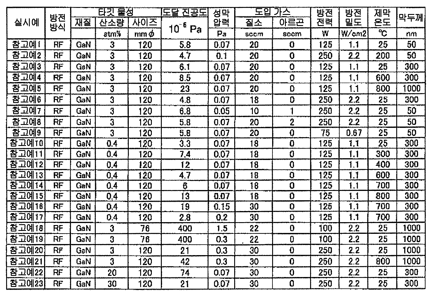
질화갈륨 스퍼터링 타깃을 사용하여, 마그네트론 스퍼터 장치로 표 3 의 조건으로 스퍼터 성막 시험을 실시하였다.Using a gallium nitride sputtering target, a sputtering film formation test was conducted under the conditions shown in Table 3 with a magnetron sputtering apparatus.
이상의 조건에서 성막을 실시한 결과, 표 4 에 나타내는 바와 같은, 질화갈륨 박막이 되었다.As a result of film formation under the above conditions, a gallium nitride thin film as shown in Table 4 was obtained.

이후, 적층막에 관한 측정예를 소개한다. 각종 평가의 측정 방법은 이하에 나타내는 바와 같다.Hereinafter, measurement examples relating to the laminated film will be introduced. Measurement methods of various evaluations are as follows.
(결정 방위, 반가폭의 측정 방법)(Method of measuring crystal orientation and half-width)
XRD 장치를 사용하여 2θ/ω 로 주사하고, 피크 위치로부터 질화갈륨, 금속 황화물의 결정 방위를 동정하고, 주된 결정 방위를 확인하였다. 그 중, 질화갈륨 (110) 면에 상당하는 피크에 대해, 2θ/ω 에서의 반가폭을 측정하였다.The crystal orientation of gallium nitride and metal sulfide was identified from the peak position by scanning with an XRD apparatus at 2? / ?, and main crystal orientation was confirmed. Among them, the half-value width at 2? /? Was measured for a peak corresponding to the gallium nitride (110) plane.
(회전 대칭성의 확인 방법)(How to confirm rotational symmetry)
XRD 장치를 사용하여 질화갈륨 박막에 대한 phi 스캔을 실시하고, 회전 대칭성을 확인하였다.A phi scan was performed on the gallium nitride thin film using an XRD device, and the rotational symmetry was confirmed.
(로킹 커브 반가폭의 측정 방법) (Method of measuring the half-width of the rocking curve)
XRD 장치를 사용하여 동정된 질화갈륨 (110) 면에 대한 ω 스캔을 실시하고, 로킹 커브 반가폭을 측정하였다.An ω scan was performed on the gallium nitride (110) surface identified using an XRD device, and the width of the rocking curve half-width was measured.
(질화갈륨 박막 중의 산소 함유량의 측정 방법)(Method for measuring the oxygen content in the gallium nitride thin film)
SIMS (2 차 이온 질량 분석계 장치명 : PHI ADEPT1010) 를 이용하고, 질화갈륨 박막에 대해, 실리콘 단결정층에 가까운 계면으로부터 50 ㎚ 의 사이의 산소량을 측정하고, 그 최소치를 산소 함유량으로 하였다. 계면으로부터 50 ㎚ 의 위치의 특정은 SIMS 측정에 의한 조성 변화로부터 각 층의 물질을 파악함으로써 확인하였다.The amount of oxygen between 50 nm was measured from the interface near the silicon single crystal layer with respect to the gallium nitride thin film using SIMS (secondary ion mass spectrometer device name: PHI ADEPT1010), and the minimum value was determined as the oxygen content. The position of 50 nm from the interface was identified by identifying the material of each layer from compositional change by SIMS measurement.
(표면 조도의 측정 방법)(Method of measuring surface roughness)
AFM 장치를 사용하여 가로 세로 10 ㎛ 의 범위에서 표면 상태를 측정하고, 그 중에서 10 ㎛ 의 길이의 측정에 있어서의 표면 조도 Ra 를 측정하였다.The surface condition was measured in the range of 10 mu m in width and 10 mu m in the AFM apparatus, and the surface roughness Ra in the measurement of the length of 10 mu m was measured therefrom.
(적층막 참고예 1)(Laminated film Reference Example 1)
2 인치 φ 의 Si (100) 단결정 기판 상에 MnS 가 50 ㎚ 제막된 기판을 이용하였다. MnS 는 (100) 면에 배향하고 있는 것을 확인하였다.A substrate having a thickness of 50 nm formed of MnS on a 2-inch Si (100) single crystal substrate was used. It was confirmed that MnS was oriented on the (100) plane.
또한, MnS/Si 박막 상에 하기의 조건으로 GaN 박막을 형성하여, 적층체로 하였다.Further, a GaN thin film was formed on the MnS / Si thin film under the following conditions to obtain a laminate.
(스퍼터 조건)(Sputter condition)
방전 방식 : RF 스퍼터 Discharge method : RF sputter
제막 장치 : 마그네트론 스퍼터 장치 Film forming apparatus : Magnetron sputtering system
타깃 사이즈 : 2 인치 φ Target size : 2 inches φ
제막 압력 : 1 ㎩ Film forming pressure : 1 Pa
도입 가스 : 아르곤 + 10 vol% 질소 Introduced gas : Argon + 10 vol% nitrogen
방전 파워 : 100 W Discharge power : 100 W
기판 온도 : 700 ℃ Substrate temperature : 700 ° C
막두께 : 10 ㎚ Film thickness : 10 nm
각종 평가의 결과는 이하에 나타내는 바와 같다.The results of various evaluations are as follows.
회전 대칭성 : 4 회 Rotational symmetry : 4 times
GaN 배향면 : (110) 면 GaN orientation plane : (110) face
2θ/ω 반가폭 : 0.7 ° 2θ / ω half full width : 0.7 °
로킹 커브 반가폭 : 3.4° Rocking curve half full width : 3.4
산소 함유량 : 3 × 10²¹ atm/㎤ Oxygen content: 3 × 10 21 atm / cm 3
(적층막 참고예 2)(Laminated film reference example 2)
적층막 참고예 1 에서 얻어진 적층체의 GaN 층 위에, 추가로 GaN 층을 기판 온도 1100 ℃ 에서 MOCVD 법으로 약 1000 ㎚ 형성하였다. 각종 평가의 결과는 이하에 나타내는 바와 같다.Laminated film A GaN layer was further formed on the GaN layer of the layered product obtained in Reference Example 1 at a substrate temperature of 1100 DEG C by MOCVD to a thickness of about 1000 nm. The results of various evaluations are as follows.
회전 대칭성 : 4 회 Rotational symmetry : 4 times
GaN 배향면 : (110) 면 GaN orientation plane : (110) face
반가폭 : 0.18° Half full width : 0.18
로킹 커브 반가폭 : 1.9° Rocking curve half full width : 1.9
산소 함유량 : 1 × 10²¹ atm/㎤ Oxygen content: 1 × 10 21 atm / cm 3
(적층막 참고예 3) (Laminated film Reference Example 3)
MnS 의 버퍼층을 형성하지 않고 직접 Si (100) 기판 상에 GaN 박막을 형성한 경우 치밀한 막을 형성할 수 없었다.When a GaN thin film was directly formed on a Si (100) substrate without forming a buffer layer of MnS, a dense film could not be formed.
본 발명을 상세하게, 또 특정의 실시양태를 참조하여 설명했지만, 본 발명의 본질과 범위를 일탈하지 않고 여러 가지 변경이나 수정을 부가할 수 있는 것은 당업자에게 있어서 분명하다.While the present invention has been described in detail and with reference to specific embodiments thereof, it will be apparent to those skilled in the art that various changes and modifications can be made without departing from the spirit and scope of the invention.
또한, 2015년 3월 30일에 출원된 일본 특허출원 2015-069913호, 2015년 4월 24일에 출원된 일본 특허출원 2015-089571호, 2015년 7월 30일에 출원된 일본 특허출원 2015-150959호, 2015년 7월 31일에 출원된 일본 특허출원 2015-152855호의 명세서, 특허 청구의 범위, 도면 및 요약서의 전체 내용을 여기에 인용하고, 본 발명의 명세서의 개시로서 받아들이는 것이다.In addition, Japanese Patent Application No. 2015-069913 filed on March 30, 2015, Japanese Patent Application No. 2015-089571 filed on April 24, 2015, Japanese Patent Application No. 2015-089571 filed on July 30, 2015, The entire contents of the specification, claims, drawings and summary of Japanese Patent Application No. 2015-152855, filed on July 31, 2015, are hereby incorporated herein by reference as if fully set forth herein.
Claims (10)
밀도가 3.0 g/㎤ 이상 5.4 g/㎤ 이하인 것을 특징으로 하는 질화갈륨계 소결체.The method according to claim 1,
And a density of 3.0 g / cm < 3 > or more and 5.4 g / cm < 3 > or less.
소결체의 평균 입경이 0.5 ㎛ 이상 3 ㎛ 이하인 것을 특징으로 하는 질화갈륨계 소결체.3. The method according to claim 1 or 2,
Wherein the sintered body has an average particle diameter of 0.5 占 퐉 or more and 3 占 퐉 or less.
소결체의 중량이 10 g 이상인 것을 특징으로 하는 질화갈륨계 소결체.4. The method according to any one of claims 1 to 3,
And the weight of the sintered body is 10 g or more.
대기 중에서 250 ℃ 의 가열 처리를 1 시간 실시해도 타깃 부재로부터 금속 갈륨의 석출을 육안으로 확인할 수 없는 것을 특징으로 하는 질화갈륨계 소결체.5. The method according to any one of claims 1 to 4,
The gallium nitride sintered body can not visually confirm the precipitation of metallic gallium from the target member even if the heat treatment at 250 캜 is performed in the air for one hour.
타깃 부재와 본딩층 사이에 텅스텐을 함유하는 층이 존재하지 않는 것을 특징으로 하는 스퍼터링 타깃.8. The method of claim 7,
And a layer containing tungsten is not present between the target member and the bonding layer.
본딩층이 인듐, 주석, 아연 중 적어도 1 성분을 함유하는 것을 특징으로 하는 스퍼터링 타깃.9. The method according to claim 7 or 8,
Wherein the bonding layer contains at least one of indium, tin and zinc.
Applications Claiming Priority (9)
| Application Number | Priority Date | Filing Date | Title |
|---|---|---|---|
| JPJP-P-2015-069913 | 2015-03-30 | ||
| JP2015069913A JP6596875B2 (en) | 2015-03-30 | 2015-03-30 | Laminate containing gallium nitride and method for manufacturing the same |
| JPJP-P-2015-089571 | 2015-04-24 | ||
| JP2015089571 | 2015-04-24 | ||
| JP2015150959 | 2015-07-30 | ||
| JPJP-P-2015-150959 | 2015-07-30 | ||
| JP2015152855 | 2015-07-31 | ||
| JPJP-P-2015-152855 | 2015-07-31 | ||
| PCT/JP2016/059341 WO2016158651A1 (en) | 2015-03-30 | 2016-03-24 | Gallium nitride-based sintered compact and method for manufacturing same |
Publications (1)
| Publication Number | Publication Date |
|---|---|
| KR20170132745A true KR20170132745A (en) | 2017-12-04 |
Family
ID=57005071
Family Applications (1)
| Application Number | Title | Priority Date | Filing Date |
|---|---|---|---|
| KR1020177026289A KR20170132745A (en) | 2015-03-30 | 2016-03-24 | Gallium nitride-based sintered compact and method for manufacturing same |
Country Status (6)
| Country | Link |
|---|---|
| US (2) | US20180072570A1 (en) |
| EP (2) | EP3998370A1 (en) |
| KR (1) | KR20170132745A (en) |
| CN (2) | CN107429383B (en) |
| TW (1) | TWI668198B (en) |
| WO (1) | WO2016158651A1 (en) |
Families Citing this family (11)
| Publication number | Priority date | Publication date | Assignee | Title |
|---|---|---|---|---|
| JP7031181B2 (en) * | 2016-09-13 | 2022-03-08 | 東ソー株式会社 | Gallium nitride based film and its manufacturing method |
| JP6953819B2 (en) * | 2017-06-15 | 2021-10-27 | 東ソー株式会社 | Gallium nitride particles and their manufacturing method |
| CN108110106B (en) * | 2017-12-14 | 2019-08-27 | 扬州乾照光电有限公司 | A kind of preparation method and LED chip of LED chip |
| TWI825187B (en) * | 2018-10-09 | 2023-12-11 | 日商東京威力科創股份有限公司 | Method for forming nitride semiconductor film |
| CN112805263A (en) * | 2018-10-10 | 2021-05-14 | 东曹株式会社 | Gallium nitride sintered body and method for producing same |
| WO2020174922A1 (en) * | 2019-02-28 | 2020-09-03 | 住友電工ハードメタル株式会社 | Polycrystalline cubic boron nitride and production method therefor |
| JP2021059483A (en) * | 2019-10-07 | 2021-04-15 | 東ソー株式会社 | Gallium nitride particles and method for their production |
| CN111153700B (en) * | 2019-12-31 | 2022-06-21 | 欧钛鑫光电科技(苏州)有限公司 | Preparation method of nitride target material |
| JP7302791B2 (en) * | 2020-05-18 | 2023-07-04 | 東京エレクトロン株式会社 | Composite target, method for manufacturing composite target, and method for forming nitride semiconductor film |
| DE112022000737T5 (en) | 2021-03-30 | 2023-11-16 | Ngk Insulators, Ltd. | sputtering target |
| WO2023182211A1 (en) * | 2022-03-25 | 2023-09-28 | 東ソー株式会社 | Gallium nitride sintered body and production method therefor |
Family Cites Families (38)
| Publication number | Priority date | Publication date | Assignee | Title |
|---|---|---|---|---|
| JPH0629239A (en) | 1992-02-27 | 1994-02-04 | Eastman Kodak Co | Manufacture of self-aligned diffused barrier in semiconductor element by making use of lift-off process and semiconductor element provided with diffused barrier |
| US6291840B1 (en) * | 1996-11-29 | 2001-09-18 | Toyoda Gosei Co., Ltd. | GaN related compound semiconductor light-emitting device |
| JPH11172424A (en) | 1997-12-12 | 1999-06-29 | Minolta Co Ltd | Production of gallium compound |
| US5942148A (en) * | 1997-12-24 | 1999-08-24 | Preston; Kenneth G. | Nitride compacts |
| EP0996173B1 (en) * | 1998-10-23 | 2015-12-30 | Xerox Corporation | Semiconductor structures including polycrystalline GaN layers and method of manufacturing |
| WO2001080311A1 (en) * | 2000-04-17 | 2001-10-25 | Virginia Commonwealth University | Defect reduction in gan and related materials |
| JP4258106B2 (en) | 2000-04-21 | 2009-04-30 | 富士電機デバイステクノロジー株式会社 | Oxide thin film element and manufacturing method thereof |
| US6861130B2 (en) | 2001-11-02 | 2005-03-01 | General Electric Company | Sintered polycrystalline gallium nitride and its production |
| JP4279533B2 (en) | 2002-09-09 | 2009-06-17 | 日鉱金属株式会社 | Sputtering target and optical recording medium |
| JP3867161B2 (en) | 2002-09-20 | 2007-01-10 | 独立行政法人物質・材料研究機構 | Thin film element |
| KR100507610B1 (en) * | 2002-11-15 | 2005-08-10 | 광주과학기술원 | Nitride semiconductor nanophase opto-electronic cell and the preparation method thereof |
| JP3924728B2 (en) * | 2003-06-30 | 2007-06-06 | 健一郎 宮原 | Electronic element |
| JP2006290729A (en) * | 2003-06-30 | 2006-10-26 | Kenichiro Miyahara | Thin film bonded body |
| CN101124353B (en) * | 2004-09-27 | 2011-12-14 | 盖利姆企业私人有限公司 | Method and apparatus for growing a group (III) metal nitride film and a group (III) metal nitride film |
| EP2573206B1 (en) * | 2004-09-27 | 2014-06-11 | Gallium Enterprises Pty Ltd | Method for growing a group (iii) metal nitride film |
| CN101068890B (en) * | 2004-12-01 | 2011-01-19 | 康乃尔研究基金会有限公司 | Group III nitride coatings and methods |
| US7772288B2 (en) * | 2004-12-01 | 2010-08-10 | Cornell Research Foundation, Inc. | Group III nitride coatings and methods |
| CN101243011B (en) * | 2005-08-24 | 2012-09-05 | 三菱化学株式会社 | Method of producing group 13 metal nitride crystal, method for manufacturing semiconductor device, and solution and melt used in those methods |
| US8946674B2 (en) * | 2005-08-31 | 2015-02-03 | University Of Florida Research Foundation, Inc. | Group III-nitrides on Si substrates using a nanostructured interlayer |
| JP2007157765A (en) * | 2005-11-30 | 2007-06-21 | Rohm Co Ltd | Gallium nitride semiconductor light emitting element |
| US8643027B2 (en) * | 2005-12-06 | 2014-02-04 | Primet Precision Materials, Inc. | Milled particle compositions and related methods and structures |
| JP4187175B2 (en) * | 2006-03-13 | 2008-11-26 | 国立大学法人東北大学 | Method for producing gallium nitride material |
| US20070234946A1 (en) * | 2006-04-07 | 2007-10-11 | Tadao Hashimoto | Method for growing large surface area gallium nitride crystals in supercritical ammonia and lagre surface area gallium nitride crystals |
| EP2543507B1 (en) * | 2010-03-02 | 2019-08-28 | Sumitomo Metal Mining Co., Ltd. | Laminate, method for producing same, and functional element using same |
| JP4720949B1 (en) | 2010-04-09 | 2011-07-13 | 住友金属鉱山株式会社 | Method for producing Cu-Ga alloy powder, Cu-Ga alloy powder, method for producing Cu-Ga alloy sputtering target, and Cu-Ga alloy sputtering target |
| CN103270000B (en) * | 2010-12-20 | 2016-02-03 | 东曹株式会社 | Gan sintered compact or gan molding and their manufacture method |
| JP2012144805A (en) * | 2010-12-21 | 2012-08-02 | Tosoh Corp | Gallium nitride molded article and method for producing the same |
| CN102226294B (en) * | 2011-05-12 | 2012-11-21 | 北京工业大学 | Modulation method for silicon-based GaN crystal structure with optimal field emission performance |
| JP5803654B2 (en) * | 2011-12-21 | 2015-11-04 | 東ソー株式会社 | Gallium nitride powder and method for producing the same |
| JP2014091851A (en) | 2012-11-02 | 2014-05-19 | Tosoh Corp | Gallium nitride target and method of producing the same |
| KR101386007B1 (en) * | 2012-11-08 | 2014-04-16 | 한국세라믹기술원 | Method for forming a gallium nitride material smiconductor substrate and substrate structure for gallium nitride material smiconductor substrate |
| JP2014224020A (en) * | 2013-05-16 | 2014-12-04 | 佐藤 忠重 | METHOD FOR MANUFACTURING A GaN SELF-STANDING SUBSTRATE |
| TWI793382B (en) * | 2013-08-08 | 2023-02-21 | 日商三菱化學股份有限公司 | SELF-SUPPORTING GaN SUBSTRATE, METHOD FOR PRODUCING GaN SINGLE CRYSTAL AND METHOD FOR PRODUCING SEMICONDUCTOR DEVICE |
| JP2015069913A (en) | 2013-09-30 | 2015-04-13 | 三菱マテリアル株式会社 | Surface-treated ito conductive film and method for producing the same |
| TWI583456B (en) | 2013-11-05 | 2017-05-21 | 王正平 | Trough-form fine blanking device |
| JP6323658B2 (en) | 2014-02-12 | 2018-05-16 | 三菱自動車工業株式会社 | Battery system for vehicles |
| JP6394936B2 (en) | 2014-02-18 | 2018-09-26 | 株式会社リコー | Image forming apparatus and driving method of image forming apparatus |
| JP6001194B2 (en) | 2014-07-18 | 2016-10-05 | キヤノンアネルバ株式会社 | Method for forming nitride semiconductor layer and method for manufacturing semiconductor device |
-
2016
- 2016-03-24 EP EP21208680.5A patent/EP3998370A1/en active Pending
- 2016-03-24 EP EP16772532.4A patent/EP3279367B1/en active Active
- 2016-03-24 KR KR1020177026289A patent/KR20170132745A/en not_active Application Discontinuation
- 2016-03-24 US US15/562,112 patent/US20180072570A1/en not_active Abandoned
- 2016-03-24 CN CN201680015322.0A patent/CN107429383B/en active Active
- 2016-03-24 CN CN202010696987.0A patent/CN111826618B/en active Active
- 2016-03-24 WO PCT/JP2016/059341 patent/WO2016158651A1/en active Application Filing
- 2016-03-29 TW TW105109830A patent/TWI668198B/en active
-
2022
- 2022-02-01 US US17/590,120 patent/US11802049B2/en active Active
Also Published As
| Publication number | Publication date |
|---|---|
| EP3279367A1 (en) | 2018-02-07 |
| CN111826618B (en) | 2022-11-01 |
| EP3279367B1 (en) | 2021-12-01 |
| US20220153582A1 (en) | 2022-05-19 |
| CN111826618A (en) | 2020-10-27 |
| TWI668198B (en) | 2019-08-11 |
| WO2016158651A1 (en) | 2016-10-06 |
| CN107429383B (en) | 2020-07-24 |
| CN107429383A (en) | 2017-12-01 |
| TW201700437A (en) | 2017-01-01 |
| US20180072570A1 (en) | 2018-03-15 |
| US11802049B2 (en) | 2023-10-31 |
| EP3998370A1 (en) | 2022-05-18 |
| EP3279367A4 (en) | 2018-10-10 |
Similar Documents
| Publication | Publication Date | Title |
|---|---|---|
| US11802049B2 (en) | Gallium nitride-based sintered compact and method for manufacturing same | |
| JP7040561B2 (en) | Gallium nitride based sintered body and its manufacturing method | |
| JP7461851B2 (en) | Semiconductor Film | |
| CN108025979B (en) | Oriented alumina substrate for epitaxial growth | |
| US20210408242A1 (en) | Semiconductor film | |
| JP2024051069A (en) | Gallium nitride sintered body and method for producing same | |
| JP7410009B2 (en) | semiconductor film | |
| WO2020075661A1 (en) | Gallium nitride-based sintered body and method for manufacturing same | |
| JP7320070B2 (en) | Underlying substrate and manufacturing method thereof | |
| JP2024040414A (en) | Gallium nitride-based sintered body and its manufacturing method | |
| WO2020195355A1 (en) | Underlying substrate | |
| JP2024032944A (en) | Gallium nitride-based sintered body and its manufacturing method | |
| WO2021064817A1 (en) | Base substrate and method for manufacturing same | |
| JPWO2020195497A1 (en) | Semiconductor film |
Legal Events
| Date | Code | Title | Description |
|---|---|---|---|
| E601 | Decision to refuse application |