KR20170123896A - Organic light emitting display device - Google Patents
Organic light emitting display device Download PDFInfo
- Publication number
- KR20170123896A KR20170123896A KR1020160053160A KR20160053160A KR20170123896A KR 20170123896 A KR20170123896 A KR 20170123896A KR 1020160053160 A KR1020160053160 A KR 1020160053160A KR 20160053160 A KR20160053160 A KR 20160053160A KR 20170123896 A KR20170123896 A KR 20170123896A
- Authority
- KR
- South Korea
- Prior art keywords
- layer
- light emitting
- organic light
- electrode
- charge blocking
- Prior art date
Links
- 230000000903 blocking effect Effects 0.000 claims abstract description 56
- 239000010409 thin film Substances 0.000 claims abstract description 24
- 239000000758 substrate Substances 0.000 claims abstract description 16
- 239000010410 layer Substances 0.000 claims description 327
- 238000002347 injection Methods 0.000 claims description 45
- 239000007924 injection Substances 0.000 claims description 45
- 238000010943 off-gassing Methods 0.000 claims description 27
- 238000000034 method Methods 0.000 claims description 19
- VYPSYNLAJGMNEJ-UHFFFAOYSA-N Silicium dioxide Chemical compound O=[Si]=O VYPSYNLAJGMNEJ-UHFFFAOYSA-N 0.000 claims description 18
- 239000010408 film Substances 0.000 claims description 18
- 229910052814 silicon oxide Inorganic materials 0.000 claims description 18
- 239000011368 organic material Substances 0.000 claims description 12
- 239000012044 organic layer Substances 0.000 claims description 11
- 239000011810 insulating material Substances 0.000 claims description 10
- 229910052581 Si3N4 Inorganic materials 0.000 claims description 9
- 229910004205 SiNX Inorganic materials 0.000 claims description 9
- HQVNEWCFYHHQES-UHFFFAOYSA-N silicon nitride Chemical compound N12[Si]34N5[Si]62N3[Si]51N64 HQVNEWCFYHHQES-UHFFFAOYSA-N 0.000 claims description 9
- 239000004642 Polyimide Substances 0.000 claims description 8
- 229920001721 polyimide Polymers 0.000 claims description 8
- 239000000463 material Substances 0.000 description 22
- 230000005525 hole transport Effects 0.000 description 17
- 239000004065 semiconductor Substances 0.000 description 13
- 238000009281 ultraviolet germicidal irradiation Methods 0.000 description 13
- 230000006798 recombination Effects 0.000 description 9
- 238000005215 recombination Methods 0.000 description 9
- -1 acryl Chemical group 0.000 description 7
- 229910052741 iridium Inorganic materials 0.000 description 7
- GKOZUEZYRPOHIO-UHFFFAOYSA-N iridium atom Chemical compound [Ir] GKOZUEZYRPOHIO-UHFFFAOYSA-N 0.000 description 7
- 229910052782 aluminium Inorganic materials 0.000 description 6
- XAGFODPZIPBFFR-UHFFFAOYSA-N aluminium Chemical compound [Al] XAGFODPZIPBFFR-UHFFFAOYSA-N 0.000 description 6
- 230000000052 comparative effect Effects 0.000 description 6
- DEVSOMFAQLZNKR-RJRFIUFISA-N (z)-3-[3-[3,5-bis(trifluoromethyl)phenyl]-1,2,4-triazol-1-yl]-n'-pyrazin-2-ylprop-2-enehydrazide Chemical compound FC(F)(F)C1=CC(C(F)(F)F)=CC(C2=NN(\C=C/C(=O)NNC=3N=CC=NC=3)C=N2)=C1 DEVSOMFAQLZNKR-RJRFIUFISA-N 0.000 description 5
- 239000000872 buffer Substances 0.000 description 5
- SECXISVLQFMRJM-UHFFFAOYSA-N N-Methylpyrrolidone Chemical compound CN1CCCC1=O SECXISVLQFMRJM-UHFFFAOYSA-N 0.000 description 4
- BQCADISMDOOEFD-UHFFFAOYSA-N Silver Chemical compound [Ag] BQCADISMDOOEFD-UHFFFAOYSA-N 0.000 description 4
- 230000015556 catabolic process Effects 0.000 description 4
- 239000004020 conductor Substances 0.000 description 4
- 239000010949 copper Substances 0.000 description 4
- 238000006731 degradation reaction Methods 0.000 description 4
- 230000006866 deterioration Effects 0.000 description 4
- ZUOUZKKEUPVFJK-UHFFFAOYSA-N diphenyl Chemical compound C1=CC=CC=C1C1=CC=CC=C1 ZUOUZKKEUPVFJK-UHFFFAOYSA-N 0.000 description 4
- 239000002019 doping agent Substances 0.000 description 4
- 230000000694 effects Effects 0.000 description 4
- 238000011156 evaluation Methods 0.000 description 4
- 239000011229 interlayer Substances 0.000 description 4
- 239000011159 matrix material Substances 0.000 description 4
- 229910052751 metal Inorganic materials 0.000 description 4
- 239000002184 metal Substances 0.000 description 4
- 239000011241 protective layer Substances 0.000 description 4
- 229910052709 silver Inorganic materials 0.000 description 4
- 239000004332 silver Substances 0.000 description 4
- 239000002356 single layer Substances 0.000 description 4
- 239000010936 titanium Substances 0.000 description 4
- 238000012546 transfer Methods 0.000 description 4
- POILWHVDKZOXJZ-ARJAWSKDSA-M (z)-4-oxopent-2-en-2-olate Chemical compound C\C([O-])=C\C(C)=O POILWHVDKZOXJZ-ARJAWSKDSA-M 0.000 description 3
- VQGHOUODWALEFC-UHFFFAOYSA-N 2-phenylpyridine Chemical compound C1=CC=CC=C1C1=CC=CC=N1 VQGHOUODWALEFC-UHFFFAOYSA-N 0.000 description 3
- OAICVXFJPJFONN-UHFFFAOYSA-N Phosphorus Chemical compound [P] OAICVXFJPJFONN-UHFFFAOYSA-N 0.000 description 3
- 239000007983 Tris buffer Substances 0.000 description 3
- XLOMVQKBTHCTTD-UHFFFAOYSA-N Zinc monoxide Chemical compound [Zn]=O XLOMVQKBTHCTTD-UHFFFAOYSA-N 0.000 description 3
- 239000000956 alloy Substances 0.000 description 3
- 229910045601 alloy Inorganic materials 0.000 description 3
- 238000006243 chemical reaction Methods 0.000 description 3
- 150000001875 compounds Chemical class 0.000 description 3
- 239000011777 magnesium Substances 0.000 description 3
- YVTHLONGBIQYBO-UHFFFAOYSA-N zinc indium(3+) oxygen(2-) Chemical compound [O--].[Zn++].[In+3] YVTHLONGBIQYBO-UHFFFAOYSA-N 0.000 description 3
- RYGMFSIKBFXOCR-UHFFFAOYSA-N Copper Chemical compound [Cu] RYGMFSIKBFXOCR-UHFFFAOYSA-N 0.000 description 2
- ZOKXTWBITQBERF-UHFFFAOYSA-N Molybdenum Chemical compound [Mo] ZOKXTWBITQBERF-UHFFFAOYSA-N 0.000 description 2
- FAPWRFPIFSIZLT-UHFFFAOYSA-M Sodium chloride Chemical compound [Na+].[Cl-] FAPWRFPIFSIZLT-UHFFFAOYSA-M 0.000 description 2
- RTAQQCXQSZGOHL-UHFFFAOYSA-N Titanium Chemical compound [Ti] RTAQQCXQSZGOHL-UHFFFAOYSA-N 0.000 description 2
- 229910021417 amorphous silicon Inorganic materials 0.000 description 2
- UMIVXZPTRXBADB-UHFFFAOYSA-N benzocyclobutene Chemical compound C1=CC=C2CCC2=C1 UMIVXZPTRXBADB-UHFFFAOYSA-N 0.000 description 2
- 235000010290 biphenyl Nutrition 0.000 description 2
- 239000004305 biphenyl Substances 0.000 description 2
- 229910052802 copper Inorganic materials 0.000 description 2
- AMGQUBHHOARCQH-UHFFFAOYSA-N indium;oxotin Chemical compound [In].[Sn]=O AMGQUBHHOARCQH-UHFFFAOYSA-N 0.000 description 2
- 229910052750 molybdenum Inorganic materials 0.000 description 2
- 239000011733 molybdenum Substances 0.000 description 2
- 230000003287 optical effect Effects 0.000 description 2
- 229920000553 poly(phenylenevinylene) Polymers 0.000 description 2
- 229920000767 polyaniline Polymers 0.000 description 2
- 229910021420 polycrystalline silicon Inorganic materials 0.000 description 2
- 229920002098 polyfluorene Polymers 0.000 description 2
- 229920000642 polymer Polymers 0.000 description 2
- 230000008569 process Effects 0.000 description 2
- 239000000243 solution Substances 0.000 description 2
- 229910052719 titanium Inorganic materials 0.000 description 2
- TYHJXGDMRRJCRY-UHFFFAOYSA-N zinc indium(3+) oxygen(2-) tin(4+) Chemical compound [O-2].[Zn+2].[Sn+4].[In+3] TYHJXGDMRRJCRY-UHFFFAOYSA-N 0.000 description 2
- ZSYMVHGRKPBJCQ-UHFFFAOYSA-N 1,1'-biphenyl;9h-carbazole Chemical group C1=CC=CC=C1C1=CC=CC=C1.C1=CC=C2C3=CC=CC=C3NC2=C1 ZSYMVHGRKPBJCQ-UHFFFAOYSA-N 0.000 description 1
- 125000001637 1-naphthyl group Chemical group [H]C1=C([H])C([H])=C2C(*)=C([H])C([H])=C([H])C2=C1[H] 0.000 description 1
- LPCWDYWZIWDTCV-UHFFFAOYSA-N 1-phenylisoquinoline Chemical compound C1=CC=CC=C1C1=NC=CC2=CC=CC=C12 LPCWDYWZIWDTCV-UHFFFAOYSA-N 0.000 description 1
- MQRCTQVBZYBPQE-UHFFFAOYSA-N 189363-47-1 Chemical compound C1=CC=CC=C1N(C=1C=C2C3(C4=CC(=CC=C4C2=CC=1)N(C=1C=CC=CC=1)C=1C=CC=CC=1)C1=CC(=CC=C1C1=CC=C(C=C13)N(C=1C=CC=CC=1)C=1C=CC=CC=1)N(C=1C=CC=CC=1)C=1C=CC=CC=1)C1=CC=CC=C1 MQRCTQVBZYBPQE-UHFFFAOYSA-N 0.000 description 1
- VFMUXPQZKOKPOF-UHFFFAOYSA-N 2,3,7,8,12,13,17,18-octaethyl-21,23-dihydroporphyrin platinum Chemical compound [Pt].CCc1c(CC)c2cc3[nH]c(cc4nc(cc5[nH]c(cc1n2)c(CC)c5CC)c(CC)c4CC)c(CC)c3CC VFMUXPQZKOKPOF-UHFFFAOYSA-N 0.000 description 1
- NBYLBWHHTUWMER-UHFFFAOYSA-N 2-Methylquinolin-8-ol Chemical compound C1=CC=C(O)C2=NC(C)=CC=C21 NBYLBWHHTUWMER-UHFFFAOYSA-N 0.000 description 1
- HONWGFNQCPRRFM-UHFFFAOYSA-N 2-n-(3-methylphenyl)-1-n,1-n,2-n-triphenylbenzene-1,2-diamine Chemical compound CC1=CC=CC(N(C=2C=CC=CC=2)C=2C(=CC=CC=2)N(C=2C=CC=CC=2)C=2C=CC=CC=2)=C1 HONWGFNQCPRRFM-UHFFFAOYSA-N 0.000 description 1
- RDBHQZLQCUALTF-UHFFFAOYSA-N 4-(4-anilinophenyl)aniline Chemical compound C1=CC(N)=CC=C1C(C=C1)=CC=C1NC1=CC=CC=C1 RDBHQZLQCUALTF-UHFFFAOYSA-N 0.000 description 1
- GMEQIEASMOFEOC-UHFFFAOYSA-N 4-[3,5-bis[4-(4-methoxy-n-(4-methoxyphenyl)anilino)phenyl]phenyl]-n,n-bis(4-methoxyphenyl)aniline Chemical compound C1=CC(OC)=CC=C1N(C=1C=CC(=CC=1)C=1C=C(C=C(C=1)C=1C=CC(=CC=1)N(C=1C=CC(OC)=CC=1)C=1C=CC(OC)=CC=1)C=1C=CC(=CC=1)N(C=1C=CC(OC)=CC=1)C=1C=CC(OC)=CC=1)C1=CC=C(OC)C=C1 GMEQIEASMOFEOC-UHFFFAOYSA-N 0.000 description 1
- MBPCKEZNJVJYTC-UHFFFAOYSA-N 4-[4-(n-phenylanilino)phenyl]aniline Chemical compound C1=CC(N)=CC=C1C1=CC=C(N(C=2C=CC=CC=2)C=2C=CC=CC=2)C=C1 MBPCKEZNJVJYTC-UHFFFAOYSA-N 0.000 description 1
- MZYDBGLUVPLRKR-UHFFFAOYSA-N 9-(3-carbazol-9-ylphenyl)carbazole Chemical compound C12=CC=CC=C2C2=CC=CC=C2N1C1=CC(N2C3=CC=CC=C3C3=CC=CC=C32)=CC=C1 MZYDBGLUVPLRKR-UHFFFAOYSA-N 0.000 description 1
- 229910016036 BaF 2 Inorganic materials 0.000 description 1
- GYHNNYVSQQEPJS-UHFFFAOYSA-N Gallium Chemical compound [Ga] GYHNNYVSQQEPJS-UHFFFAOYSA-N 0.000 description 1
- 229910018068 Li 2 O Inorganic materials 0.000 description 1
- FYYHWMGAXLPEAU-UHFFFAOYSA-N Magnesium Chemical compound [Mg] FYYHWMGAXLPEAU-UHFFFAOYSA-N 0.000 description 1
- YNPNZTXNASCQKK-UHFFFAOYSA-N Phenanthrene Natural products C1=CC=C2C3=CC=CC=C3C=CC2=C1 YNPNZTXNASCQKK-UHFFFAOYSA-N 0.000 description 1
- 229920001609 Poly(3,4-ethylenedioxythiophene) Polymers 0.000 description 1
- 229910010413 TiO 2 Inorganic materials 0.000 description 1
- DGEZNRSVGBDHLK-UHFFFAOYSA-N [1,10]phenanthroline Chemical compound C1=CN=C2C3=NC=CC=C3C=CC2=C1 DGEZNRSVGBDHLK-UHFFFAOYSA-N 0.000 description 1
- PJRJXFPRMUZBHQ-UHFFFAOYSA-N [Ir].C1C=CC2=CC=CC=C2N1C1=CC=CC=C1.C1C=CC2=CC=CC=C2N1C1=CC=CC=C1.C1C=CC2=CC=CC=C2N1C1=CC=CC=C1 Chemical compound [Ir].C1C=CC2=CC=CC=C2N1C1=CC=CC=C1.C1C=CC2=CC=CC=C2N1C1=CC=CC=C1.C1C=CC2=CC=CC=C2N1C1=CC=CC=C1 PJRJXFPRMUZBHQ-UHFFFAOYSA-N 0.000 description 1
- CUJRVFIICFDLGR-UHFFFAOYSA-N acetylacetonate Chemical compound CC(=O)[CH-]C(C)=O CUJRVFIICFDLGR-UHFFFAOYSA-N 0.000 description 1
- NIXOWILDQLNWCW-UHFFFAOYSA-N acrylic acid group Chemical group C(C=C)(=O)O NIXOWILDQLNWCW-UHFFFAOYSA-N 0.000 description 1
- QVQLCTNNEUAWMS-UHFFFAOYSA-N barium oxide Inorganic materials [Ba]=O QVQLCTNNEUAWMS-UHFFFAOYSA-N 0.000 description 1
- UHOVQNZJYSORNB-UHFFFAOYSA-N benzene Substances C1=CC=CC=C1 UHOVQNZJYSORNB-UHFFFAOYSA-N 0.000 description 1
- HFACYLZERDEVSX-UHFFFAOYSA-N benzidine Chemical compound C1=CC(N)=CC=C1C1=CC=C(N)C=C1 HFACYLZERDEVSX-UHFFFAOYSA-N 0.000 description 1
- 125000000319 biphenyl-4-yl group Chemical group [H]C1=C([H])C([H])=C([H])C([H])=C1C1=C([H])C([H])=C([*])C([H])=C1[H] 0.000 description 1
- XZCJVWCMJYNSQO-UHFFFAOYSA-N butyl pbd Chemical compound C1=CC(C(C)(C)C)=CC=C1C1=NN=C(C=2C=CC(=CC=2)C=2C=CC=CC=2)O1 XZCJVWCMJYNSQO-UHFFFAOYSA-N 0.000 description 1
- XJHCXCQVJFPJIK-UHFFFAOYSA-M caesium fluoride Inorganic materials [F-].[Cs+] XJHCXCQVJFPJIK-UHFFFAOYSA-M 0.000 description 1
- 239000003990 capacitor Substances 0.000 description 1
- 125000004432 carbon atom Chemical group C* 0.000 description 1
- 150000001793 charged compounds Chemical class 0.000 description 1
- 239000000470 constituent Substances 0.000 description 1
- 238000010276 construction Methods 0.000 description 1
- 238000010924 continuous production Methods 0.000 description 1
- XCJYREBRNVKWGJ-UHFFFAOYSA-N copper(II) phthalocyanine Chemical compound [Cu+2].C12=CC=CC=C2C(N=C2[N-]C(C3=CC=CC=C32)=N2)=NC1=NC([C]1C=CC=CC1=1)=NC=1N=C1[C]3C=CC=CC3=C2[N-]1 XCJYREBRNVKWGJ-UHFFFAOYSA-N 0.000 description 1
- 230000003247 decreasing effect Effects 0.000 description 1
- 230000009977 dual effect Effects 0.000 description 1
- 230000005281 excited state Effects 0.000 description 1
- 229910052733 gallium Inorganic materials 0.000 description 1
- 239000011521 glass Substances 0.000 description 1
- 230000005283 ground state Effects 0.000 description 1
- 239000012535 impurity Substances 0.000 description 1
- 229910052738 indium Inorganic materials 0.000 description 1
- APFVFJFRJDLVQX-UHFFFAOYSA-N indium atom Chemical compound [In] APFVFJFRJDLVQX-UHFFFAOYSA-N 0.000 description 1
- 150000002484 inorganic compounds Chemical class 0.000 description 1
- 229910010272 inorganic material Inorganic materials 0.000 description 1
- CECAIMUJVYQLKA-UHFFFAOYSA-N iridium 1-phenylisoquinoline Chemical compound [Ir].C1=CC=CC=C1C1=NC=CC2=CC=CC=C12.C1=CC=CC=C1C1=NC=CC2=CC=CC=C12.C1=CC=CC=C1C1=NC=CC2=CC=CC=C12 CECAIMUJVYQLKA-UHFFFAOYSA-N 0.000 description 1
- UEEXRMUCXBPYOV-UHFFFAOYSA-N iridium;2-phenylpyridine Chemical compound [Ir].C1=CC=CC=C1C1=CC=CC=N1.C1=CC=CC=C1C1=CC=CC=N1.C1=CC=CC=C1C1=CC=CC=N1 UEEXRMUCXBPYOV-UHFFFAOYSA-N 0.000 description 1
- 239000004973 liquid crystal related substance Substances 0.000 description 1
- PQXKHYXIUOZZFA-UHFFFAOYSA-M lithium fluoride Inorganic materials [Li+].[F-] PQXKHYXIUOZZFA-UHFFFAOYSA-M 0.000 description 1
- FQHFBFXXYOQXMN-UHFFFAOYSA-M lithium;quinolin-8-olate Chemical compound [Li+].C1=CN=C2C([O-])=CC=CC2=C1 FQHFBFXXYOQXMN-UHFFFAOYSA-M 0.000 description 1
- 229910052749 magnesium Inorganic materials 0.000 description 1
- SJCKRGFTWFGHGZ-UHFFFAOYSA-N magnesium silver Chemical compound [Mg].[Ag] SJCKRGFTWFGHGZ-UHFFFAOYSA-N 0.000 description 1
- 239000007769 metal material Substances 0.000 description 1
- 230000005012 migration Effects 0.000 description 1
- 238000013508 migration Methods 0.000 description 1
- OKPMSRGLGBBULD-UHFFFAOYSA-N n,n-diphenyl-9,9'-spirobi[fluorene]-1-amine Chemical compound C1=CC=CC=C1N(C=1C=2C3(C4=CC=CC=C4C4=CC=CC=C43)C3=CC=CC=C3C=2C=CC=1)C1=CC=CC=C1 OKPMSRGLGBBULD-UHFFFAOYSA-N 0.000 description 1
- IBHBKWKFFTZAHE-UHFFFAOYSA-N n-[4-[4-(n-naphthalen-1-ylanilino)phenyl]phenyl]-n-phenylnaphthalen-1-amine Chemical compound C1=CC=CC=C1N(C=1C2=CC=CC=C2C=CC=1)C1=CC=C(C=2C=CC(=CC=2)N(C=2C=CC=CC=2)C=2C3=CC=CC=C3C=CC=2)C=C1 IBHBKWKFFTZAHE-UHFFFAOYSA-N 0.000 description 1
- 125000002560 nitrile group Chemical group 0.000 description 1
- 230000001151 other effect Effects 0.000 description 1
- KYKLWYKWCAYAJY-UHFFFAOYSA-N oxotin;zinc Chemical compound [Zn].[Sn]=O KYKLWYKWCAYAJY-UHFFFAOYSA-N 0.000 description 1
- 238000002161 passivation Methods 0.000 description 1
- 230000035515 penetration Effects 0.000 description 1
- 125000002080 perylenyl group Chemical group C1(=CC=C2C=CC=C3C4=CC=CC5=CC=CC(C1=C23)=C45)* 0.000 description 1
- CSHWQDPOILHKBI-UHFFFAOYSA-N peryrene Natural products C1=CC(C2=CC=CC=3C2=C2C=CC=3)=C3C2=CC=CC3=C1 CSHWQDPOILHKBI-UHFFFAOYSA-N 0.000 description 1
- IEQIEDJGQAUEQZ-UHFFFAOYSA-N phthalocyanine Chemical compound N1C(N=C2C3=CC=CC=C3C(N=C3C4=CC=CC=C4C(=N4)N3)=N2)=C(C=CC=C2)C2=C1N=C1C2=CC=CC=C2C4=N1 IEQIEDJGQAUEQZ-UHFFFAOYSA-N 0.000 description 1
- 239000004033 plastic Substances 0.000 description 1
- 229920003023 plastic Polymers 0.000 description 1
- 125000002924 primary amino group Chemical group [H]N([H])* 0.000 description 1
- 239000011347 resin Substances 0.000 description 1
- 229920005989 resin Polymers 0.000 description 1
- 230000004044 response Effects 0.000 description 1
- 239000011780 sodium chloride Substances 0.000 description 1
- XOLBLPGZBRYERU-UHFFFAOYSA-N tin dioxide Chemical compound O=[Sn]=O XOLBLPGZBRYERU-UHFFFAOYSA-N 0.000 description 1
- 229910001887 tin oxide Inorganic materials 0.000 description 1
- ODHXBMXNKOYIBV-UHFFFAOYSA-N triphenylamine Chemical compound C1=CC=CC=C1N(C=1C=CC=CC=1)C1=CC=CC=C1 ODHXBMXNKOYIBV-UHFFFAOYSA-N 0.000 description 1
- 239000011787 zinc oxide Substances 0.000 description 1
Images


Classifications
-
- H—ELECTRICITY
- H10—SEMICONDUCTOR DEVICES; ELECTRIC SOLID-STATE DEVICES NOT OTHERWISE PROVIDED FOR
- H10K—ORGANIC ELECTRIC SOLID-STATE DEVICES
- H10K59/00—Integrated devices, or assemblies of multiple devices, comprising at least one organic light-emitting element covered by group H10K50/00
- H10K59/10—OLED displays
- H10K59/12—Active-matrix OLED [AMOLED] displays
- H10K59/124—Insulating layers formed between TFT elements and OLED elements
-
- H01L27/3258—
-
- H01L27/3246—
-
- H01L27/3248—
-
- H01L27/3262—
-
- H01L27/3272—
-
- H01L51/5016—
-
- H01L51/5088—
-
- H01L51/5256—
-
- H—ELECTRICITY
- H10—SEMICONDUCTOR DEVICES; ELECTRIC SOLID-STATE DEVICES NOT OTHERWISE PROVIDED FOR
- H10K—ORGANIC ELECTRIC SOLID-STATE DEVICES
- H10K50/00—Organic light-emitting devices
- H10K50/10—OLEDs or polymer light-emitting diodes [PLED]
- H10K50/11—OLEDs or polymer light-emitting diodes [PLED] characterised by the electroluminescent [EL] layers
-
- H—ELECTRICITY
- H10—SEMICONDUCTOR DEVICES; ELECTRIC SOLID-STATE DEVICES NOT OTHERWISE PROVIDED FOR
- H10K—ORGANIC ELECTRIC SOLID-STATE DEVICES
- H10K50/00—Organic light-emitting devices
- H10K50/10—OLEDs or polymer light-emitting diodes [PLED]
- H10K50/17—Carrier injection layers
-
- H—ELECTRICITY
- H10—SEMICONDUCTOR DEVICES; ELECTRIC SOLID-STATE DEVICES NOT OTHERWISE PROVIDED FOR
- H10K—ORGANIC ELECTRIC SOLID-STATE DEVICES
- H10K50/00—Organic light-emitting devices
- H10K50/80—Constructional details
- H10K50/84—Passivation; Containers; Encapsulations
- H10K50/844—Encapsulations
- H10K50/8445—Encapsulations multilayered coatings having a repetitive structure, e.g. having multiple organic-inorganic bilayers
-
- H—ELECTRICITY
- H10—SEMICONDUCTOR DEVICES; ELECTRIC SOLID-STATE DEVICES NOT OTHERWISE PROVIDED FOR
- H10K—ORGANIC ELECTRIC SOLID-STATE DEVICES
- H10K59/00—Integrated devices, or assemblies of multiple devices, comprising at least one organic light-emitting element covered by group H10K50/00
- H10K59/10—OLED displays
- H10K59/12—Active-matrix OLED [AMOLED] displays
- H10K59/121—Active-matrix OLED [AMOLED] displays characterised by the geometry or disposition of pixel elements
- H10K59/1213—Active-matrix OLED [AMOLED] displays characterised by the geometry or disposition of pixel elements the pixel elements being TFTs
-
- H—ELECTRICITY
- H10—SEMICONDUCTOR DEVICES; ELECTRIC SOLID-STATE DEVICES NOT OTHERWISE PROVIDED FOR
- H10K—ORGANIC ELECTRIC SOLID-STATE DEVICES
- H10K59/00—Integrated devices, or assemblies of multiple devices, comprising at least one organic light-emitting element covered by group H10K50/00
- H10K59/10—OLED displays
- H10K59/12—Active-matrix OLED [AMOLED] displays
- H10K59/122—Pixel-defining structures or layers, e.g. banks
-
- H—ELECTRICITY
- H10—SEMICONDUCTOR DEVICES; ELECTRIC SOLID-STATE DEVICES NOT OTHERWISE PROVIDED FOR
- H10K—ORGANIC ELECTRIC SOLID-STATE DEVICES
- H10K59/00—Integrated devices, or assemblies of multiple devices, comprising at least one organic light-emitting element covered by group H10K50/00
- H10K59/10—OLED displays
- H10K59/12—Active-matrix OLED [AMOLED] displays
- H10K59/123—Connection of the pixel electrodes to the thin film transistors [TFT]
-
- H—ELECTRICITY
- H10—SEMICONDUCTOR DEVICES; ELECTRIC SOLID-STATE DEVICES NOT OTHERWISE PROVIDED FOR
- H10K—ORGANIC ELECTRIC SOLID-STATE DEVICES
- H10K59/00—Integrated devices, or assemblies of multiple devices, comprising at least one organic light-emitting element covered by group H10K50/00
- H10K59/10—OLED displays
- H10K59/12—Active-matrix OLED [AMOLED] displays
- H10K59/126—Shielding, e.g. light-blocking means over the TFTs
-
- H01L2251/301—
-
- H01L2251/558—
-
- H—ELECTRICITY
- H10—SEMICONDUCTOR DEVICES; ELECTRIC SOLID-STATE DEVICES NOT OTHERWISE PROVIDED FOR
- H10K—ORGANIC ELECTRIC SOLID-STATE DEVICES
- H10K2102/00—Constructional details relating to the organic devices covered by this subclass
-
- H—ELECTRICITY
- H10—SEMICONDUCTOR DEVICES; ELECTRIC SOLID-STATE DEVICES NOT OTHERWISE PROVIDED FOR
- H10K—ORGANIC ELECTRIC SOLID-STATE DEVICES
- H10K2102/00—Constructional details relating to the organic devices covered by this subclass
- H10K2102/301—Details of OLEDs
- H10K2102/351—Thickness
Abstract
Description
본 발명은 유기 발광 표시 장치에 관한 것으로서, 보다 상세하게는 외광에 의한 수명 저하를 최소화할 수 있는 유기 발광 표시 장치에 관한 것이다.BACKGROUND OF THE INVENTION 1. Field of the Invention [0001] The present invention relates to an organic light emitting diode display, and more particularly, to an organic light emitting diode display capable of minimizing lifetime degradation due to external light.
유기 발광 표시 장치(OLED)는 자체 발광형 표시 장치로서, 전자(electron) 주입을 위한 전극(cathode)과 정공(hole) 주입을 위한 전극(anode)으로부터 각각 전자와 정공을 발광층 내부로 주입시켜, 주입된 전자와 정공이 결합한 엑시톤(exciton)이 여기 상태로부터 기저 상태로 떨어질 때 발광하는 유기 발광 소자를 이용한 표시 장치이다. The organic light emitting diode (OLED) is a self-luminous display device in which electrons and holes are injected into the light emitting layer from an anode for injecting electrons and an anode for injecting holes, And emits light when an exciton in which injected electrons and holes are coupled falls from an excited state to a ground state.
유기 발광 표시 장치는 빛이 방출되는 방향에 따라서 상부 발광(Top Emission) 방식, 하부 발광(Bottom Emission) 방식 및 양면 발광(Dual Emission) 방식 등으로 나누어지고, 구동 방식에 따라서는 수동 매트릭스형(Passive Matrix)과 능동 매트릭스형(Active Matrix) 등으로 나누어질 수 있다.The organic light emitting display device is classified into a top emission type, a bottom emission type, and a dual emission type depending on a direction in which light is emitted, and a passive matrix type Matrix) and an active matrix (active matrix).
유기 발광 표시 장치는 액정 표시 장치(LCD)와는 달리 별도의 광원이 필요하지 않아 경량 박형으로 제조가 가능하다. 또한, 유기 발광 표시 장치는 저전압 구동에 의해 소비 전력 측면에서 유리할 뿐만 아니라, 색상 구현, 응답 속도, 시야각, 명암비(contrast ratio: CR)도 우수하여, 차세대 디스플레이 장치로서 연구되고 있다.Unlike a liquid crystal display (LCD), an organic light emitting display does not require a separate light source and can be manufactured in a light and thin shape. In addition, the organic light emitting display device is not only advantageous from the viewpoint of power consumption by low voltage driving, but also has excellent color reproduction, response speed, viewing angle, and contrast ratio (CR) and is being studied as a next generation display device.
유기 발광 표시 장치의 사용 목적에 따라, 유기 발광 표시 장치가 외부에서 장시간 사용되어 외광에 장시간 노출되는 경우, 유기 발광 표시 장치의 발광 성능 및 수명이 저하될 수 있다. According to the use purpose of the organic light emitting display, if the organic light emitting display is used for a long period of time and exposed to external light for a long time, the light emitting performance and lifetime of the organic light emitting display may be reduced.
특히, 자연광에 포함된 UV(Ultra Violet)에 유기 발광 표시 장치가 지속적으로 노출되는 경우, 유기 발광 표시 장치에 포함된 유기 발광 소자가 손상되면서 유기 발광 표시 장치의 수명이 저하되는 문제가 발생할 수 있다. Particularly, when the organic light emitting display device is continuously exposed to UV (Ultra Violet) included in natural light, the organic light emitting device included in the organic light emitting display device may be damaged and the lifetime of the organic light emitting display device may be reduced .
이에 본 발명의 발명자는 외광에 의한 수명 저하를 최소화할 수 있는 유기 발광 표시 장치를 발명하였다. Accordingly, the inventor of the present invention has invented an organic light emitting display device capable of minimizing the deterioration of lifetime due to external light.
본 발명의 실시예에 따른 해결 과제는 유기 발광 소자의 하부에 무기 절연 물질로 이루어진 전하 차단층을 구성함으로써 외광에 의한 유기 발광 소자의 손상 및 수명의 저하를 최소화할 수 있는 유기 발광 표시 장치를 제공하는 것을 목적으로 한다.A problem to be solved by the present invention is to provide an organic light emitting display device capable of minimizing damage to organic light emitting devices due to external light and minimized lifetime by forming a charge blocking layer made of an inorganic insulating material below the organic light emitting devices .
본 발명의 실시예에 따른 해결 과제들은 이상에서 언급한 과제들로 제한되지 않으며, 언급되지 않은 또 다른 과제들은 아래의 기재로부터 당업자에게 명확하게 이해될 수 있을 것이다.The solutions according to the embodiments of the present invention are not limited to the above-mentioned problems, and other problems not mentioned can be clearly understood by those skilled in the art from the following description.
전술한 바와 같은 과제를 해결하기 위하여 외광에 의한 유기 발광 소자의 수명 저하를 최소화할 수 있는 유기 발광 표시 장치가 제공된다.In order to solve the above-described problems, an organic light emitting display device capable of minimizing the lifetime of the organic light emitting device due to external light is provided.
본 발명의 실시예에 따른 유기 발광 표시 장치는 기판에 있는 박막 트랜지스터와 박막 트랜지스터 상에 배치된 평탄화층과 평탄화층 상에 배치되고, 박막 트랜지스터와 접속된 제 1 전극과 제 1 전극의 일측 상에 배치되고, 제 1 전극의 일부를 노출시키는 뱅크와 제 1 전극 상에 배치된 발광부와 발광부 상에 배치된 제 2 전극 및 평탄화층과 뱅크 사이에 배치된 전하 차단층을 포함한다.An organic light emitting display according to an embodiment of the present invention includes a thin film transistor on a substrate, a planarization layer disposed on the thin film transistor, a first electrode connected to the thin film transistor and a first electrode connected to the planarization layer, A bank for exposing a portion of the first electrode, a light emitting portion disposed on the first electrode, a second electrode disposed on the light emitting portion, and a charge blocking layer disposed between the planarization layer and the bank.
또 다른 측면에서 본 발명의 실시예에 따른 제 1 전극과 제 2 전극 사이에 하나 이상의 유기물층과 유기 발광층으로 이루어진 유기 발광 소자를 포함하는 유기 발광 표시 장치는 외광에 의해 유기 발광 소자 하부에 위치하는 평탄화층에서 발생한 아웃 개싱(out-gassing)에 의해 유기 발광 소자의 수명이 저하되지 않도록 구성된 전하 차단층을 구비한다. According to another aspect of the present invention, there is provided an organic light emitting diode display including an organic light emitting diode comprising at least one organic layer and an organic light emitting layer between a first electrode and a second electrode according to an embodiment of the present invention, And a charge blocking layer configured to prevent the lifetime of the organic light emitting device from being degraded by out-gassing occurring in the layer.
기타 실시예의 구체적인 사항들은 상세한 설명 및 도면들에 포함되어 있다.The details of other embodiments are included in the detailed description and drawings.
본 발명의 실시예에 따른 유기 발광 표시 장치는 발광부 하부에 구성된 무기 절연 물질로 이루어진 전하 차단층이 외광에 의해 발생하는 평탄화층의 아웃 개싱(out-gassing)에 의한 음전하가 뱅크를 통해 정공 주입층으로 이동하는 것을 최소화함으로써 발광부로의 정공 주입 특성이 향상될 수 있다. The organic light emitting diode display according to an embodiment of the present invention includes a charge blocking layer made of an inorganic insulating material formed under the light emitting portion, and a negative charge by out-gassing of a planarization layer generated by external light is injected through the bank, By minimizing the movement to the layer, the hole injection characteristic to the light emitting portion can be improved.
또한 본 발명의 실시예에 따른 유기 발광 표시 장치는 발광부 하부에 구성된 전하 차단층이 아웃 개싱에 의한 음전하의 이동 경로를 차단하고 유기 발광 소자의 재결합 영역이 유지되도록 함으로써 유기 발광 표시 장치의 수명이 향상될 수 있다.Also, the organic light emitting diode display according to an embodiment of the present invention includes a charge blocking layer formed at a lower portion of a light emitting portion to block a negative charge transfer path due to outgassing and to maintain a recombination region of the organic light emitting diode, Can be improved.
또한 본 발명의 실시예에 따른 유기 발광 표시 장치는 발광부 하부에 구성된 전하 차단층이 외광에 의해 발생하는 평탄화층의 아웃 개싱으로부터 유기 발광 소자를 보호함으로써 유기 발광 표시 장치의 성능 및 신뢰성이 개선될 수 있다.In addition, the organic light emitting display device according to an embodiment of the present invention improves the performance and reliability of the OLED display by protecting the OLED from the outgassing of the planarization layer generated by the external light, .
본 발명의 효과는 이상에서 언급한 효과에 제한되지 않으며, 언급되지 않은 또 다른 효과는 아래의 기재로부터 당업자에게 명확하게 이해될 수 있을 것이다.The effects of the present invention are not limited to the effects mentioned above, and other effects not mentioned can be clearly understood by those skilled in the art from the following description.
이상에서 해결하고자 하는 과제, 과제 해결 수단, 효과에 기재한 발명의 내용이 청구항의 필수적인 특징을 특정하는 것은 아니므로, 청구항의 권리범위는 발명의 내용에 기재된 사항에 의하여 제한되지 않는다.The scope of the claims is not limited by the matters described in the contents of the invention, as the contents of the invention described in the problems, the solutions to the problems and the effects to be solved do not specify essential features of the claims.
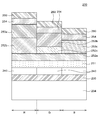
도 1은 외광에 의한 유기 발광 표시 장치의 수명 저하 현상을 설명하기 위한 개략적인 단면도이다.
도 2는 본 발명의 실시예에 따른 유기 발광 표시 장치의 단면 구조를 나타내는 도면이다.
도 3은 본 발명의 실시예에 따른 유기 발광 표시 장치의 유기 발광 소자 단면 구조를 확대하여 나타낸 도면이다.
도 4는 도 2에서 도시한 본 발명의 실시예에 따른 유기 발광 표시 장치의 X 영역을 확대하여 나타낸 도면이다.
도 5a 및 도 5b는 비교예와 본 발명의 실시예에 따른 유기 발광 표시 장치의 UV 조사 전/후 수명 평가 결과를 나타내는 도면이다. 1 is a schematic cross-sectional view for explaining a phenomenon in which the lifetime of the organic light emitting diode display device is degraded by external light.
2 is a cross-sectional view illustrating an organic light emitting display according to an exemplary embodiment of the present invention.
3 is an enlarged view of a cross-sectional structure of an organic light emitting diode of an OLED display according to an exemplary embodiment of the present invention.
FIG. 4 is an enlarged view of an X region of the organic light emitting diode display according to the embodiment of the present invention shown in FIG. 2. Referring to FIG.
FIGS. 5A and 5B are graphs showing the evaluation results of the life before and after UV irradiation of the organic light emitting diode display according to the comparative example and the present invention. FIG.
본 발명의 이점 및 특징, 그리고 그것들을 달성하는 방법은 첨부되는 도면과 함께 상세하게 후술되어 있는 실시예들을 참조하면 명확해질 것이다. 그러나, 본 발명은 이하에서 개시되는 실시예들에 한정되는 것이 아니라 서로 다른 다양한 형태로 구현될 것이며, 단지 본 실시예들은 본 발명의 개시가 완전하도록 하며, 본 발명이 속하는 기술 분야에서 통상의 지식을 가진 자에게 발명의 범주를 완전하게 알려주기 위해 제공되는 것이며, 본 발명은 청구항의 범주에 의해 정의될 뿐이다.BRIEF DESCRIPTION OF THE DRAWINGS The advantages and features of the present invention and the manner of achieving them will become apparent with reference to the embodiments described in detail below with reference to the accompanying drawings. It should be understood, however, that the invention is not limited to the disclosed embodiments, but is capable of many different forms and should not be construed as limited to the embodiments set forth herein. Rather, these embodiments are provided so that this disclosure will be thorough and complete, To fully disclose the scope of the invention to those skilled in the art, and the invention is only defined by the scope of the claims.
본 발명의 실시예를 설명하기 위한 도면에 개시된 형상, 크기, 비율, 각도, 개수 등은 예시적인 것이므로 본 발명이 도시된 사항에 한정되는 것은 아니다. 명세서 전체에 걸쳐 동일 참조 부호는 동일 구성 요소를 지칭한다. 또한, 본 발명을 설명함에 있어서, 관련된 공지 기술에 대한 구체적인 설명이 본 발명의 요지를 불필요하게 흐릴 수 있다고 판단되는 경우 그 상세한 설명은 생략한다. 본 명세서 상에서 언급된 '포함한다', '갖는다', '이루어진다' 등이 사용되는 경우 '~만'이 사용되지 않는 이상 다른 부분이 추가될 수 있다. 구성 요소를 단수로 표현한 경우에 특별히 명시적인 기재 사항이 없는 한 복수를 포함하는 경우를 포함한다.The shapes, sizes, ratios, angles, numbers, and the like disclosed in the drawings for describing the embodiments of the present invention are illustrative, and thus the present invention is not limited thereto. Like reference numerals refer to like elements throughout the specification. In the following description, well-known functions or constructions are not described in detail since they would obscure the invention in unnecessary detail. Where the terms "comprises", "having", "done", and the like are used in this specification, other portions may be added unless "only" is used. Unless the context clearly dictates otherwise, including the plural unless the context clearly dictates otherwise.
구성 요소를 해석함에 있어서, 별도의 명시적 기재가 없더라도 오차 범위를 포함하는 것으로 해석한다. 위치 관계에 대한 설명일 경우, 예를 들어, '~상에', '~상부에', '~하부에', '~옆에' 등으로 두 부분의 위치 관계가 설명되는 경우, '바로' 또는 '직접'이 사용되지 않는 이상 두 부분 사이에 하나 이상의 다른 부분이 위치할 수도 있다.In interpreting the constituent elements, it is construed to include the error range even if there is no separate description. In the case of a description of the positional relationship, for example, if the positional relationship between two parts is described as 'on', 'on top', 'under', and 'next to' Or " direct " is not used, one or more other portions may be located between the two portions.
또한 제 1, 제 2 등이 다양한 구성 요소들을 서술하기 위해서 사용되나, 이들 구성 요소들은 이들 용어에 의해 제한되지 않는다. 이들 용어들은 단지 하나의 구성 요소를 다른 구성 요소와 구별하기 위하여 사용하는 것이다. 따라서, 이하에서 언급되는 제 1 구성 요소는 본 발명의 기술적 사상 내에서 제 2 구성 요소일 수도 있다.Also, the first, second, etc. are used to describe various components, but these components are not limited by these terms. These terms are used only to distinguish one component from another. Therefore, the first component mentioned below may be the second component within the technical spirit of the present invention.
본 발명의 여러 실시예들의 각각 특징들이 부분적으로 또는 전체적으로 서로 결합 또는 조합 가능하고, 기술적으로 다양한 연동 및 구동이 가능하며, 각 실시예들이 서로에 대하여 독립적으로 실시 가능할 수도 있고 연관 관계로 함께 실시할 수도 있다.It is to be understood that each of the features of the various embodiments of the present invention may be combined or combined with each other, partially or wholly, technically various interlocking and driving, and that the embodiments may be practiced independently of each other, It is possible.
이하, 도면을 참조하여 본 발명에 대해 상세히 설명한다. Hereinafter, the present invention will be described in detail with reference to the drawings.
도 1은 외광에 의한 유기 발광 표시 장치의 수명 저하 현상을 설명하기 위한 개략적인 단면도이다.1 is a schematic cross-sectional view for explaining a phenomenon in which the lifetime of the organic light emitting diode display device is degraded by external light.
도 1을 참조하면, 종래의 유기 발광 표시 장치는 기판의 상부를 평탄화하는 평탄화층(34), 유기 발광층(53)에 정공을 공급하는 애노드(40), 유기 발광층(53)을 포함하는 발광부(50), 유기 발광층(53)에 전자를 공급하는 캐소드(60)가 순차적으로 적층되어 있고, 인접하여 위치하는 복수의 서브 화소 영역들을 구분하기 위한 뱅크(45)를 포함한다.Referring to FIG. 1, a conventional organic light emitting display includes a
또한 도 1을 참조하면, 상기 발광부(50)는 정공 주입층(51), 정공 수송층(52), 전자 수송층(54)을 포함하는 복수의 유기물층 및 유기 발광층(53)을 포함할 수 있다. 1, the
유기 발광 표시 장치가 장시간 UV에 노출되는 경우, 발광부(50) 또는 애노드(40)와 인접하는 유기물층으로부터 발생한 아웃 개싱(out gassing)에 의해 발광부(50)가 손상을 받을 수 있다. When the organic light emitting display device is exposed to UV for a long time, the
보다 구체적으로, 발광부(50)에 인접한 애노드(40)의 하부에 배치된 평탄화층(34)은 일반적으로 폴리이미드(Polyimide, PI) 또는 아크릴(acryl)과 같은 유기 물질로 구성된다. 이러한 폴리이미드 또는 아크릴과 같은 유기 물질은 UV 조사에 의해 NMP(N-Methyl-2-Pyrrolidone), 헥산니트릴(Hexanitrile)과 같은 부분적으로 음전하를 띄는 가스 화합물(70)을 형성한다. More specifically, the
구체적으로, 헥산니트릴의 나이트릴기(-CN)는 양전하가 탄소 원자들로 가로막혀 있고 음전하가 외곽으로 돌출되어 있는 전하 분포(charge distribution)를 가지고 있다. 이러한 음전하를 띄는 가스 화합물(70)은 평탄화층(34)으로부터 밖으로 배출되는데, 도 1에 도시한 것과 같이 가스 화합물(70)은 인접하여 위치하는 뱅크(45)를 통해서 발광부(50)를 구성하는 유기물층과 반응한다. Specifically, the nitrile group (-CN) of hexanitrile has a charge distribution in which a positive charge is blocked by carbon atoms and a negative charge protrudes to the outside. The
이 때, 가스 화합물(70)은 발광부(50) 중 최하단에 위치하고 뱅크(45)와 인접하여 배치된 정공 주입층(51)을 구성하는 양전하를 띄는 화합물과 반응하게 된다. 이러한 가스 화합물(70)과의 반응에 의해 정공 주입층(51)을 이루는 물질들은 양전하를 잃게 되고, 유기 발광층(53)으로 원활하게 정공을 주입할 수 없게 된다.At this time, the
이와 같이, 종래 유기 발광 표시 장치에 강한 UV가 조사되거나 또는 유기 발광 표시 장치가 장시간 UV에 노출되는 경우, 정공 주입층(51)의 유기 발광층(53)으로의 정공 주입 성능이 저하되면서 구동 전압 증가, 휘도 감소 및 수명 저하와 같이 유기 발광 표시 장치의 성능이 저하되는 문제가 발생할 수 있다. As described above, when strong UV is applied to the organic light emitting display device or when the organic light emitting display device is exposed to UV for a long time, the hole injection performance of the
또한 유기 발광 표시 장치에 포함된 유기 발광 소자의 수명의 경우, 정공과 전자가 재결합하여 엑시톤을 형성하여 발광하는 재결합 영역(recombination zone)의 위치에 따라 영향을 받을 수 있다. Further, in the case of the lifetime of the organic light emitting diode included in the organic light emitting display, the hole and the electron may recombine to form an exciton, which may be influenced by the position of the recombination zone emitting light.
유기 발광 표시 장치는 애노드에서 형성된 정공과 캐소드에서 형성된 전자가 유기 발광층으로 이동하고, 유기 발광층에서 정공과 전자가 재결합하여 엑시톤을 형성함으로써 빛을 발광한다. 여기서 재결합 영역은 유기 발광층 내 정공과 전자가 재결합하여 엑시톤이 형성되는 영역을 의미한다. In the organic light emitting diode display, holes formed in the anode and electrons formed in the cathode move to the organic light emitting layer, and holes and electrons recombine in the organic light emitting layer to emit light by forming excitons. Here, the recombination region means a region in which an exciton is formed by recombination of holes and electrons in the organic light emitting layer.
도 1을 참조하면, 외광을 통해 유기 발광 표시 장치에 강한 UV가 조사되거나 유기 발광 표시 장치가 장시간 UV에 노출되는 경우, 상술한 바와 같이, 발광부(50)에 인접한 애노드(40)의 하부에 배치된 평탄화층(34)에서 발생한 아웃 개싱에 의해 정공 주입층(51)이 손상을 받아 정공 주입 성능이 저하된다. Referring to FIG. 1, when strong UV is applied to the organic light emitting display through external light or when the organic light emitting display is exposed to UV for a long time, The hole injecting
이와 같이 유기 발광층 내 정공 주입 특성이 떨어지는 경우, 정공과 전자의 재결합 영역이 유기 발광층 내에서 정공 주입층(51) 쪽에 가깝게 형성된다. 이러한 경우, 재결합 영역이 유기 발광층 내 중앙부에 형성되는 경우와 대비할 때 엑시톤들이 더 빨리 소멸되어 유기 발광 표시 장치의 수명이 저하될 수 있다. When the hole injection characteristics in the organic light emitting layer are deteriorated, a recombination region of holes and electrons is formed in the organic light emitting layer close to the
특히 유기 발광층(53)이 인광 재료의 유기 발광층인 경우, 엑시톤 충돌에 의한 삼중항-삼중항 소멸(triplet-triplet annihilation, TTA)이 빠르게 진행되어 열화가 일어날 수 있다. 과도하게 빠른 엑시톤 간의 충돌로 인해, 동일한 구동 전압에서 발광 가능한 여기된 엑시톤의 수가 현저히 감소하게 되어 유기 발광 표시 장치의 수명이 저하될 수 있다.Particularly, in the case where the organic
도 2는 본 발명의 실시예에 따른 유기 발광 표시 장치의 단면 구조를 나타내는 도면이다. 2 is a cross-sectional view illustrating an organic light emitting display according to an exemplary embodiment of the present invention.
도 2를 참조하면, 본 발명의 실시예에 따른 유기 발광 표시 장치(200)는 기판(210), 기판(210) 상에 위치하는 박막 트랜지스터(Thin Film Transistor, 220) 및 제 1 전극(240)과 제 2 전극(260) 사이에 위치하고 복수의 유기물층과 유기 발광층(Organic Emitting Layer)을 포함하는 발광부(250)를 포함하여 구성된다. 2, an
유기 발광 표시 장치(200)는 복수의 서브 화소(sub pixel)를 포함한다. 서브 화소는 실제 빛이 발광되는 최소 단위의 영역을 말한다. 또한, 복수의 서브 화소가 모여 백색의 광을 표현할 수 있는 최소의 군으로 이루어질 수 있으며, 예를 들어, 세 개의 서브 화소가 하나의 군으로서, 적색 서브 화소, 녹색 서브 화소 및 청색 화소 서브가 하나의 군을 이룰 수 있다. 그러나, 이에 한정된 것은 아니며, 다양한 서브 화소 설계가 가능하다. 도 2에서는 설명의 편의를 위해 유기 발광 표시 장치(200)의 복수의 서브 화소 중 하나의 서브 화소만을 도시하였다.The
본 발명의 실시예에 따른 유기 발광 표시 장치(200)에 있어서 기판(210)은 유기 발광 표시 장치(200)의 다양한 구성 요소들을 지지하기 위한 것으로 절연 물질로 형성된다. 예를 들어서, 기판(210)은 글래스(Glass) 뿐만 아니라, PET(Polyethylen Terephthalate), PEN(Polyethylen Naphthalate), 폴리이미드(Polyimide) 등의 플라스틱 기판 등으로 이루어질 수 있다.In the organic light emitting
기판(210) 상에는 기판(210) 및 외부로부터의 불순 원소의 침투를 차단하고 상기 유기 발광 표시 장치(200)의 다양한 구성 요소들을 보호하기 위한 버퍼층(231)이 형성될 수 있다. 버퍼층(231)은 예를 들어 실리콘 산화막(SiOx) 또는 실리콘 질화막(SiNx)의 단일층 또는 복수층 구조로 형성될 수 있다. 버퍼층(231)은 유기 발광 표시 장치(200)의 구조나 특성에 따라 생략될 수도 있다.A
버퍼층(231) 상에는 반도체층(222), 게이트 절연층(232), 게이트 전극(221), 층간 절연층(233), 소스 전극(223) 및 드레인 전극(224)이 배치되고, 게이트 전극(221), 반도체층(222), 소스 전극(223) 및 드레인 전극(224)을 포함하는 박막 트랜지스터(220)가 형성된다. A
구체적으로, 기판(210) 상에 반도체층(222)이 형성되고, 반도체층 (222) 상에 반도체층(222)과 게이트 전극(221)을 절연시키기 위한 게이트 절연층(232)이 형성된다. 게이트 전극(221) 상에는 게이트 전극(221)과 소스 전극(223) 및 드레인 전극(224)을 절연시키기 위한 층간 절연층(233)이 형성된다. 층간 절연층(233) 상에는 반도체층(222)과 각각 접하는 소스 전극(223) 및 드레인 전극(224)이 형성된다. 소스 전극(223) 및 드레인 전극(224)은 컨택홀을 통해 반도체층(222)과 전기적으로 연결된다.Specifically, a
반도체층(222)은 비정질 실리콘(amorphous silicon: a-Si), 다결정 실리콘(polycrystalline silicon: poly-Si), 산화물(oxide) 반도체 또는 유기물 (organic) 반도체 등으로 형성될 수 있다. 반도체층(222)이 산화물 반도체로 이루어지는 경우, IGZO(Indium Gallium Zinc Oxide), ZTO(Zinc Tin Oxide), IZO(Indium Zinc Oxide) 또는 ITZO(Indium Tin Zinc Oxide) 중 어느 하나의 물질로 이루어질 수 있으나 이에 한정되지 않는다.The
게이트 절연층(232)은 실리콘 산화막(SiOx), 실리콘 질화막(SiNx) 등과 같은 무기 절연 물질 이루어진 단일층 또는 복수층 구조로 형성될 수 있다. The
게이트 전극(221)은 게이트 신호를 박막 트랜지스터(220)에 전달하는 기능을 수행하고, 알루미늄(Al), 몰리브덴(Mo), 티타늄(Ti), 구리(Cu) 중 적어도 하나 이상의 금속 또는 합금으로 이루어질 수 있고, 상기 금속 또는 물질의 단일층 또는 복수층 구조로 형성될 수 있다. The
소스 전극(224)과 드레인 전극(223)은 외부에서 전달되는 전기적인 신호가 박막 트랜지스터(220)에서 발광부(250)로 전달되도록 하는 역할을 한다. 소스 전극(224)과 드레인 전극(223)은 알루미늄(Al), 몰리브덴(Mo), 티타늄(Ti), 구리(Cu) 중 적어도 하나 이상의 금속 또는 합금으로 이루어질 수 있고, 상기 금속 또는 물질의 단일층 또는 복수층 구조로 형성될 수 있다.The
본 명세서에서는 설명의 편의를 위해, 유기 발광 표시 장치(200)에 포함될 수 있는 다양한 박막 트랜지스터 중 제 1 전극(240)과 연결된 구동 박막 트랜지스터(220)만을 도시하였다. 각각의 서브 화소는 스위칭 박막 트랜지스터나 커패시터 등이 더 포함될 수 있다.Only the driving
박막 트랜지스터(220) 상에는 보호층(270) 및 평탄화층(234)이 형성된다. 보호층(270)은 무기 절연 물질로 이루어질 수 있다. 예를 들어, 보호층(270)은 실리콘 산화막(SiOx) 또는 실리콘 질화막(SiNx) 등으로 이루어질 수 있으나 이에 한정되지 않는다. 또한 평탄화층(234)은 기판(210) 상부를 평탄화하는 기능을 한다. 평탄화층(234)은 단일층 또는 복수층으로 구성될 수 있으며, 유기 물질로 이루어질 수 있다. 예를 들어, 평탄화층(234)은 폴리이미드(Polyimide) 또는 포토아크릴(Photo Acryl)로 이루어질 수 있다. 보호층(270) 및 평탄화층(234)은 각각의 서브 화소에서 박막 트랜지스터(220)와 제 1 전극(240)을 전기적으로 연결하기 위한 컨택홀을 포함한다. A
또한 도 2를 참조하면, 본 발명의 실시예에 따른 유기 발광 표시 장치(200)의 평탄화층(234) 상에는 전하 차단층(235)이 형성된다. 즉, 상기 전하 차단층(235)은 평탄화층(234)과 제 1 전극(240)의 사이, 그리고 평탄화층(234)과 뱅크(245)의 사이에 배치될 수 있다. Referring to FIG. 2, a
전하 차단층(235)은 유기 발광 표시 장치(200)가 외부 광 또는 UV에 의해 유기 물질로 이루어진 평탄화층(234)의 아웃 개싱(out-gassing)에 의해 발생한 음전하가 뱅크(245)를 통해서 유기물층인 정공 주입층(251)으로 이동하는 것을 최소화하는 역할을 한다. The
전하 차단층(235)은 평탄화층(234)에서 발생하는 아웃 개싱(out-gassing)에 의한 음전하의 이동 경로를 차단할 수 있도록 무기 절연 물질로 이루어질 수 있다. 예를 들어서, 전하 차단층(235)은 실리콘 산화막(SiOx)과 실리콘 질화막(SiNx) 중 적어도 하나를 포함하여 이루어질 수 있다. The
또한 유기 발광 표시 장치에서 요구되는 전하 차단 특성에 따라서 전하 차단층(235)은 실리콘 산화막(SiOx)과 실리콘 질화막(SiNx) 중 적어도 하나를 포함하는 복수의 무기 절연층이 적층된 구조로 이루어질 수도 있다.In addition, the
또한 전하 차단층(235)은 유기 발광 표시 장치에서 요구되는 전하 차단 특성 및 공정적인 측면을 고려할 때, 500Å 내지 5000Å의 두께를 갖도록 형성될 수 있다. Also, the
제 1 전극(240)은 평탄화층(234) 상에 형성된다. 제 1 전극(240)은 애노드(anode)일 수 있으며, 일함수 값이 비교적 큰 도전성 물질로 형성되어 유기 발광층(253)으로 정공을 공급하는 역할을 한다. 제 1 전극(240)은 평탄화층(234)의 컨택홀을 통해 박막 트랜지스터(220)와 전기적으로 연결되고, 예를 들어서, 박막 트랜지스터(220)의 소스 전극(223)과 전기적으로 연결될 수 있다. 또한 제 1 전극(240)은 화소 별로 이격되어 배치된다. 제 1 전극(240)은 투명 도전성 물질로 형성되고, 예를 들어, 인듐 주석 산화물(Indium Tin Oxide, ITO), 인듐 아연 산화물(Indium Zin Oxide, IZO) 등과 같은 물질로 형성될 수 있다.The
또한 본 발명의 실시예에 따른 유기 발광 표시 장치(200)가 상부 발광 방식(Top Emission)인 경우, 유기 발광층(253)로부터 발광된 광이 제 1 전극(240)에 반사되어 보다 원활하게 상부 방향으로 방출될 수 있도록, 제 1 전극(240)의 상부 또는 하부에 반사 효율이 우수한 금속 물질, 예를 들면, 알루미늄(Al) 또는 은(Ag)과 같은 물질로 이루어진 반사층이 추가로 형성될 수 있다.Also, when the organic light emitting
예를 들어, 제 1 전극(240)은 투명 도전성 물질로 형성된 투명 도전층과 반사층이 차례로 적층된 2층 구조이거나, 투명 도전층, 반사층 및 투명 도전층이 차례로 적층된 3층 구조일 수 있다. 반사층은 은(Ag) 또는 은을 포함하는 합금일 수 있으며, 예를 들어서 은(Ag) 또는 APC(Ag/Pd/Cu)일 수 있다.For example, the
본 발명의 실시예를 설명함에 있어서 상부 발광 방식(Top Emission)은 유기 발광층(253)으로부터 발광되는 광이 제 2 전극(260)의 방향으로 출사되는 방식을 의미하고, 하부 발광 방식(Bottom Emission)은 상부 발광 방식과 반대의 방향인 제 1 전극(240)의 방향으로 광이 출사되는 방식을 의미한다.In the description of the embodiment of the present invention, the top emission means a method in which light emitted from the
제 1 전극(240) 및 전하 차단층(235) 상에 뱅크(245)가 형성된다. 뱅크(245)는 인접하는 서브 화소 영역을 구분하며, 제 1 전극(240)의 일측 상에 배치되어 제 1 전극(240)의 일부를 노출시킨다. 또한, 뱅크(245)는 복수의 서브 화소 영역으로 구성된 화소 영역을 구분할 수도 있다. 이때, 뱅크(245)는 발광부(250)와 접촉하며, 보다 구체적으로, 정공 주입층(251)에 직접 접촉할 수 있다. 또한 뱅크(245)는 유기 물질로 이루어질 수 있다. 예를 들어, 뱅크(245)는 폴리이미드(polyimide), 아크릴(acryl) 또는 벤조사이클로부텐(benzocyclobutene; BCB)계 수지로 이루어질 수 있으나, 이에 한정되지 않는다.A
제 2 전극(260)은 제 1 전극(240) 상에 형성된다. 제 2 전극(260)은 캐소드(cathode)일 수 있으며, 유기 발광층(253)으로 전자를 공급하여야 하므로 일함수가 낮은 도전성 물질로 형성된다. 보다 구체적으로, 제 2 전극(260)은 마그네슘(Mg), 은-마그네슘(Ag:Mg) 등과 같은 금속 물질일 수 있다. A second electrode (260) is formed on the first electrode (240). The
또한, 본 발명의 실시예에 따른 유기 발광 표시 장치(200)가 상부 발광 방식인 경우, 제 2 전극(260)은 인듐 주석 산화물(Indium Tin Oxide, ITO), 인듐 아연 산화물(Indium Zin Oxide, IZO), 인듐 주석 아연 산화물(Indium Tin Zinc Oxide, ITZO), 아연 산화물(Zinc Oxide, ZnO) 및 주석 산화물(Tin Oxide, TiO) 계열의 투명 도전성 산화물로 이루어질 수 있다.When the
제 1 전극(240)과 뱅크(245) 상에 발광부(250)가 형성된다. 발광부(250)는 필요에 따라 다양한 유기물층이 포함할 수 있으며, 또한 유기 발광층(253)을 필수적으로 포함하여 구성된다. 상기 유기물층은 적어도 하나의 정공 주입층(251), 정공 수송층(252) 및 전자 수송층(254)을 포함하여 이루어질 수 있다. A
도 3은 본 발명의 실시예에 따른 유기 발광 표시 장치의 유기 발광 소자의 단면 구조를 확대하여 나타낸 도면이다. 3 is an enlarged view of a cross-sectional structure of an organic light emitting diode of an OLED display according to an embodiment of the present invention.
이하 도 3을 참조하여 본 발명의 실시예에 따른 유기 발광 표시 장치(200)의 발광부(250)에 대해서 보다 구체적으로 설명한다.Hereinafter, the
도 3을 참조하면, 본 발명의 실시예에 따른 유기 발광 표시 장치(200)의 발광부(250)는 제 1 전극(240) 상에 배치된 정공 주입층(251, Hole Injection Layer: HIL), 정공 주입층(251) 상에 배치된 제 1 정공 수송층(252a, 1st Hole Transport Layer: 1st HTL), 제 1 정공 수송층(252a) 상에 배치된 제 2 정공 수송층(252b, 2nd Hole Transport Layer: 2nd HTL) 및 제 3 정공 수송층(252c, 3rd Hole Transport Layer: 3rd HTL), 정공 수송층(252a, 252b, 252c) 상에 배치된 적색 발광층(253a), 녹색 발광층(253b) 및 청색 발광층(253c)을 포함하는 유기 발광층(Organic Emitting Layer: EML) 및 유기 발광층 상에 배치된 전자 수송층(254, Electron Transport Layer: ETL)을 포함한다. 3, the
또한 도 3을 참조하면, 본 발명의 실시예에 따른 유기 발광 표시 장치(200)는 평탄화층(234)과 제 1 전극(240) 사이에 배치되고, 유기물층 하부에 배치된 전하 차단층(235)을 포함하여 구성된다. 3, an
제 1 전극(240)은 기판 상에 정의된 적색 서브 화소 영역(R), 녹색 서브 화소 영역(G) 및 청색 서브 화소 영역(B) 각각에 대응되도록 전하 차단층(235) 상에 배치된다. The
정공 주입층(251)은 적색 서브 화소 영역(R), 녹색 서브 화소 영역(G) 및 청색 서브 화소 영역(B) 모두에 대응되도록 공통층으로 제 1 전극(240) 상에 배치된다. The
정공 주입층(251)은 정공의 주입을 원활하게 하는 역할을 할 수 있으며, HATCN(1,4,5,8,9,11-hexaazatriphenylene-hexanitrile), CuPc(cupper phthalocyanine), PEDOT(poly(3,4)-ethylenedioxythiophene), PANI(polyaniline), NPD(N,N-dinaphthyl-N,N'-diphenylbenzidine), TPD(N,N'-Bis(3-methylphenyl)-N,N′'-bis(phenyl)-benzidine), α-NPB(Bis[N-(1-naphthyl)-N-phenyl]benzidine), TDAPB(1,3,5-tris(4-diphenylaminophenyl)benzene), TCTA(Tris(4-carbazoyl-9-yl)triphenylamine), spiro-TAD(2,2',7,7′'-Tetrakis(N,N-diphenylamino)-9,9-spirobifluorene) 및 CBP(4,4’-bis(carbazol-9-yl)biphenyl) 중 적어도 하나 이상의 물질로 이루어질 수 있으나 이에 한정되지 않는다.The
정공 주입층(251)은 제 1 정공 수송층(252a)을 구성하는 물질에 p형 도펀트(p-dopant)를 도핑하여 형성될 수도 있다. 이러한 경우 하나의 공정 장비에서 연속 공정으로 정공 주입층(251)과 제 2 정공 수송층(252a)을 형성할 수 있다. 상기 p형 도펀트는 F4-TCNQ(2,3,5,6-tetrafluoro-7,7,8,8-tetracyanl-quinidimethane)로 이루어질 수 있으나 이에 한정되지 않는다.The
제 1 정공 수송층(252a)은 적색 서브 화소 영역(R), 녹색 서브 화소 영역(G) 및 청색 서브 화소 영역(B) 모두에 대응되도록 공통층으로 정공 주입층(251) 상에 배치된다. 제 1 정공 수송층(252a)은 정공의 수송을 원활하게 하는 역할을 하며, NPD(N,N-dinaphthyl-N,N'-diphenylbenzidine), TPD(N,N'-bis-(3-methylphenyl)-N,N'-bis-(phenyl)-benzidine), spiro-TAD(2,2',7,7′'-Tetrakis(N,N-diphenylamino)-9,9-spirobifluorene) 및 MTDATA(4,4',4"-Tris(N-3-methylphenyl-N-phenyl-amino)-triphenylamine) 중 어느 하나 이상으로 이루어질 수 있으나 이에 한정되지 않는다.The first
제 2 정공 수송층(252b)은 적색 서브 화소 영역(R)의 제 1 정공 수송층(252a) 상에 배치된다. 또한 제 3 정공 수송층(252c)은 녹색 서브 화소 영역(G)의 제 1 정공 수송층(252a) 상에 배치된다. The second
제 2 정공 수송층(252b) 및 제 3 정공 수송층(252c)은 정공 주입층(251)으로부터 적색 발광층(253a)과 녹색 발광층(253b) 각각에 정공을 원활하게 전달하는 역할을 한다. The second
또한 제 2 정공 수송층(252b) 및 제 3 정공 수송층(252c)의 각각의 두께는 마이크로 캐비티(micro cavity)의 광학적 거리를 형성할 수 있다. 보다 구체적으로, 제 2 정공 수송층(252b) 및 제 3 정공 수송층(252c) 각각의 두께는 적색 발광층(253a)이 제 1 전극(240)와 제 2 전극(260) 사이에서 마이크로 캐비티 구조를 형성하도록, 그리고 녹색 발광층(253b)이 제 1 전극(240)와 제 2 전극(260) 사이에서 마이크로 캐비티 구조를 형성하도록 결정될 수 있으며, 적색 서브 화소 영역(R)과 녹색 서브 화소 영역(G)에서 마이크로 캐비티의 광학적 거리를 형성하여 유기 발광 표시 장치(200)의 효율을 향상시킬 수 있다.The thickness of each of the second
유기 발광층은 인광 발광층 또는 형광 발광층을 포함하여 이루어진다. 구체적으로, 유기 발광층은 적색 발광층(253a), 녹색 발광층(253b) 또는 청색 발광층(253c)일 수 있으며, 각각 인광 물질 또는 형광 물질로 이루어질 수 있다. The organic luminescent layer comprises a phosphorescent or luminescent layer. Specifically, the organic luminescent layer may be a red
적색 발광층(253a)은 적색 서브 화소 영역(R)의 제 2 정공 수송층(252b) 상에 배치된다. 적색 발광층(253a)은 적색을 발광하는 발광 물질을 포함할 수 있으며, 인광 물질 또는 형광 물질을 이용하여 형성될 수 있다. And the red
보다 구체적으로 적색 발광층(253a)은 CBP(carbazole biphenyl) 또는 mCP(1,3-bis(carbazol-9-yl)benzene)를 포함하는 호스트 물질을 포함할 수 있으며, Ir(btp)2(acac)(bis(2-benzo[b]thiophen-2-yl-pyridine)(acetylacetonate)iridium(III)), Ir(piq)2(acac)(bis(1-phenylisoquinoline)(acetylacetonate)iridium(III)), Ir(piq)3(tris(1-phenylquinoline)iridium(III)) 및 PtOEP(octaethylporphyrin platinum) 중 어느 하나 이상을 포함하는 도펀트를 포함하는 인광 물질로 이루어질 수 있고, 이와는 달리 PBD:Eu(DBM)3(Phen) 또는 Perylene을 포함하는 형광 물질로 이루어질 수 있으나 이에 한정되지 않는다.
More specifically, the red
녹색 발광층(253b)은 녹색 서브 화소 영역(G)의 제 3 정공 수송층(252c) 상에 배치된다. 녹색 발광층(253b)은 녹색을 발광하는 발광 물질을 포함할 수 있으며, 인광 물질 또는 형광 물질을 이용하여 형성될 수 있다.The green
보다 구체적으로 녹색 발광층(253b)은 CBP 또는 mCP를 포함하는 호스트 물질을 포함할 수 있으며, Ir(ppy)3(tris(2-phenylpyridine)iridium(III)) 또는 Ir(ppy)2(acaa)(bis(2-phenylpyridine)(acetylacetonate)iridium(III)를 포함하는 이리듐 착물(Ir complex)과 같은 도펀트 물질을 포함하는 인광 물질로 이루어질 수 있고, 이와는 달리 Alq3(tris(8-hydroxyquinolino)aluminum)을 포함하는 형광 물질로 이루어질 수 있으나 이에 한정되지 않는다.More specifically, the green
청색 발광층(253c)은 청색 서브 화소 영역의 제 1 정공 수송층(252a) 상에 배치된다. 청색 발광층(253c)은 청색을 발광하는 발광 물질을 포함할 수 있으며, 인광 물질 또는 형광 물질을 이용하여 형성될 수 있다. And the blue
보다 구체적으로 청색 발광층(253c)은 CBP 또는 mCP를 포함하는 호스트 물질을 포함할 수 있으며, FIrPic(bis(3,5,-difluoro-2-(2-pyridyl)phenyl-(2-carboxypyridyl)iridium(III))을 포함하는 도펀트 물질을 포함하는 인광 물질로 이루어질 수 있다. 또한, DPVBi(4,4'-bis[4-di-p-tolylamino)stryl)biphenyl), DSA(1-4-di-[4-(N,N-di-phenyl)amino]styryl-benzene), PFO(polyfluorene)계 고분자 및 PPV(polyphenylenevinylene)계 고분자 중 어느 하나를 포함하는 형광 물질로 이루어질 수 있으나 이에 한정되지 않는다.More specifically, the blue light-emitting
전자 수송층(254)은 적색 서브 화소 영역(R), 녹색 서브 화소 영역(G) 및 청색 서브 화소 영역(B) 모두에 대응되도록 적색 발광층(253a), 녹색 발광층(253b) 및 청색 발광층(253c) 상에 배치된다. The
전자 수송층(254)은 전자의 수송 및 주입의 역할을 할 수 있으며, 전자 수송층(254)의 두께는 전자 수송 특성을 고려하여 조절될 수 있다. The thickness of the
전자 수송층(254)은 전자의 수송을 원활하게 하는 역할을 하며, Liq(8-hydroxyquinolinolato-lithium), Alq3(tris(8-hydroxyquinolino)aluminum), PBD(2-(4-biphenylyl)-5-(4-tert-butylpheny)-1,3,4oxadiazole), TAZ(3-(4-biphenyl)4-phenyl-5-tert-butylphenyl-1,2,4-triazole), spiro-PBD 및 BAlq(bis(2-methyl-8-quinolinolate)-4-(phenylphenolato)aluminium) 중 어느 하나 이상으로 이루어질 수 있으나 이에 한정되지 않는다.The
또한 전자 주입층(electron injection layer: EIL)을 전자 수송층(254) 상에 추가로 구성하는 것도 가능하다. Further, an electron injection layer (EIL) may be further formed on the
전자 주입층(EIL)은 BaF2, LiF, NaCl, CsF, Li2O 및 BaO와 같은 금속 무기 화합물로 이루어질 수 있으나 이에 한정되지 않는다.The electron injection layer (EIL) may be made of metal inorganic compounds such as BaF 2 , LiF, NaCl, CsF, Li 2 O, and BaO, but is not limited thereto.
여기서, 본 발명의 실시예에 따라 그 구조가 한정되는 것은 아니며, 정공 주입층(251), 제 1 정공 수송층(252a), 제 2 정공 수송층(252b), 제 3 정공 수송층(253c), 전자 수송층(254) 중에서 적어도 어느 하나가 생략될 수도 있다. 또한, 정공 주입층(251), 제 1 정공 수송층(252a), 제 2 정공 수송층(252b), 제 3 정공 수송층(253c), 전자 수송층(254) 중 어느 하나를 두 개 이상의 층으로 형성하는 것도 가능하다.Here, the structure is not limited according to the embodiment of the present invention, and the structure of the
제 2 전극(260)은 적색 서브 화소 영역(R), 녹색 서브 화소 영역(G) 및 청색 서브 화소 영역(B) 모두에 대응되도록 전자 수송층(254) 상에 배치된다. The
캡핑층(Capping layer)은 제 2 전극(260) 상에 배치될 수 있다. 캡핑층은 유기 발광 표시 장치의 광 추출 효과를 향상시키기 위한 것으로, 제 1 정공 수송층(252a), 전자 수송층(254), 적색 발광층(253a), 녹색 발광층(253b), 청색 발광층(253c)의 호스트 물질 중 어느 하나로 이루어질 수 있다. 또한 상기 캡핑층은 유기 발광 표시 장치(200)의 구조나 특성에 따라 생략하는 것이 가능하다.The capping layer may be disposed on the
그리고, 본 발명의 실시예에 따른 유기 발광 표시 장치는 TV, 모바일(Mobile), 테블릿 PC(Tablet PC), 모니터(Monitor), 노트북 컴퓨터(Laptop Computer), 차량용 표시 장치, 및 차량용 조명 장치 등을 포함한 표시 장치 등에 적용될 수 있다. 또는, 웨어러블(wearable) 표시 장치, 폴더블(foldable) 표시 장치, 및 롤러블(rollable) 표시 장치 등에도 적용될 수 있다.The organic light emitting display according to an embodiment of the present invention may be applied to various devices such as a TV, a mobile, a tablet PC, a monitor, a laptop computer, a vehicle display device, And the like. Or a wearable display device, a foldable display device, and a rollable display device.
도 4는 도 2에서 도시한 본 발명의 실시예에 따른 유기 발광 표시 장치의 X 영역을 확대하여 나타낸 도면이다.FIG. 4 is an enlarged view of an X region of the organic light emitting diode display according to the embodiment of the present invention shown in FIG. 2. Referring to FIG.
앞서 설명한 바와 같이 유기 발광 표시 장치가 외부 광 또는 UV에 장시간 노출되는 경우, 평탄화층의 아웃 개싱(out-gassing)에 의해 발생한 음전하를 띄는 가스 화합물이 상기 평탄화층과 인접하여 위치하는 뱅크를 통해 이동하면서 뱅크 상에 인접한 발광부를 구성하는 유기물층과 반응할 수 있다.As described above, when the organic light emitting display device is exposed to external light or UV for a long time, a gaseous compound having a negative charge generated by out-gassing of the planarization layer moves through a bank located adjacent to the planarization layer And can react with the organic material layer constituting the adjacent light emitting portion on the bank.
이와 같이 평탄화층의 아웃 개싱에 의한 음전하를 띄는 가스 화합물과 뱅크 상에 인접한 정공 주입층 물질과의 반응에 의해 유기 발광층으로 정공 주입 성능이 저하되면서 유기 발광 표시 장치의 구동 전압 증가, 휘도 감소 및 수명 저하와 같은 문제가 발생하였다.As a result of the reaction between the gaseous compound having a negative charge by the outgassing of the planarization layer and the adjacent hole injection layer material on the bank, the hole injection performance of the organic emission layer is lowered and the driving voltage of the organic emission display, Problems such as deterioration occurred.
도 4를 참조하면, 본 발명의 실시예에 따른 유기 발광 표시 장치(200)의 경우, 외광에 의해 제 1 전극(240)의 하부에 위치하는 평탄화층(234)의 아웃 개싱에 의해 발생한 음전하가 뱅크(245)를 통해서 인접한 유기물층인 정공 주입층(251)으로 이동하는 것을 최소화하는 전하 차단층(235)을 포함하여 구성된다. 보다 구체적으로, 상기 전하 차단층(235)은 평탄화층(234)과 제 1 전극(240)의 사이, 그리고 평탄화층(234)과 뱅크(245)의 사이에 배치될 수 있다.Referring to FIG. 4, in the case of the
상기 전하 차단층(235)은 유기 발광 표시 장치(200)가 외부 광 또는 UV에 의해 평탄화층(234)의 아웃 개싱(out-gassing)에 의해 발생한 음전하를 띄는 가스 화합물(290)이 뱅크(245)를 통해서 유기물층인 정공 주입층(251)으로 이동하는 경로를 차단하는 역할을 한다.The
즉, 본 발명의 실시예에 따른 유기 발광 표시 장치(200)는 발광부(250) 하부에 구성된 무기 절연 물질로 이루어진 전하 차단층(235)이 외광에 의해 발생하는 평탄화층(234)의 아웃 개싱(out-gassing)에 의한 음전하가 뱅크(245)를 통해 정공 주입층(251)으로 이동하는 것을 차단하여 정공 주입층(251)과의 반응을 최소화함으로써 발광부(250)로의 정공 주입 특성이 향상될 수 있다. That is, in the organic light emitting
또한 본 발명의 실시예에 따른 유기 발광 표시 장치(200)는 발광부(250) 하부에 구성된 전하 차단층(235)이 아웃 개싱에 의한 음전하의 이동 경로를 차단하고 유기 발광 소자의 재결합 영역이 유지되도록 함으로써 유기 발광 표시 장치의 수명이 향상될 수 있다.In addition, the organic light emitting
또한 본 발명의 실시예에 따른 유기 발광 표시 장치(200)는 발광부(250) 하부에 구성된 전하 차단층(235)이 외광에 의해 발생하는 평탄화층(234)의 아웃 개싱으로부터 유기 발광 소자를 보호함으로써 유기 발광 표시 장치의 성능 및 신뢰성이 개선될 수 있다.The organic light emitting
도 5a 및 도 5b는 비교예와 본 발명의 실시예에 따른 유기 발광 표시 장치의 UV 조사 전/후 수명 평가 결과를 나타내는 도면이다. FIGS. 5A and 5B are graphs showing the evaluation results of the life before and after UV irradiation of the organic light emitting diode display according to the comparative example and the present invention. FIG.
비교예의 경우, 전하 차단층을 포함하지 않는 유기 발광 표시 장치의 UV 조사 전/후 수명 평가 결과를 나타낸 것이며, 실시예의 경우, 발광부 하부에 전하 차단층을 포함하는 유기 발광 표시 장치의 UV 조사 전/후 수명 평가 결과를 나타낸 것이다. In the case of the comparative example, the evaluation results of the life before / after UV irradiation of the organic light emitting display device not including the charge blocking layer are shown. In the case of the embodiment, before the UV irradiation of the organic light emitting display device including the charge blocking layer below the light emitting portion / After-life evaluation result.
여기서, 유기 발광 표시 장치의 UV 조사에 따른 수명 저하 현상을 평가하기 위하여, 각각의 유기 발광 표시 장치에 420nm 파장의 UV를 2.4W/m2의 세기로 80시간 동안 조사하였다. 또한 유기 발광 표시 장치의 수명은 40에서 20.5mA/cm2의 전류 밀도로 전류를 인가하는 조건에서 휘도를 측정하여 평가하였다. Here, in order to evaluate the lifetime degradation phenomenon caused by UV irradiation of the organic light emitting display device, each of the organic light emitting display devices was irradiated with UV of 420 nm wavelength at an intensity of 2.4 W / m 2 for 80 hours. Also, the lifetime of the organic light emitting display device was evaluated by measuring the luminance under the condition of applying current at a current density of 40 to 20.5 mA / cm 2 .
우선 도 5a를 참조하여 비교예에 따른 유기 발광 표시 장치의 UV 조사 전/후 수명을 살펴보면, 초기 발광 휘도의 95% 수준의 발광 휘도를 나타내는데 까지의 시간, 즉 유기 발광 표시 장치의 95% 수명(T95)이 UV 조사 전에 비해 UV 조사 후에 약 70% 수준으로 크게 저하됨을 알 수 있다. 즉, 종래 유기 발광 표시 장치의 경우, UV 조사에 의해 정공 주입층의 성능이 저하되고, 이로 인해 UV 조사 후의 수명이 크게 저하됨을 알 수 있다. Referring to FIG. 5A, the lifetime before and after the UV irradiation of the organic light emitting display according to the comparative example is about 95% of the initial light emission luminance, that is, the 95% T95) was significantly reduced to about 70% after UV irradiation compared with before UV irradiation. That is, in the case of the conventional organic light emitting display, the performance of the hole injection layer is lowered by UV irradiation, and the lifetime after UV irradiation is greatly lowered.
반면, 도 5b를 참조하여 본 발명의 실시예에 따른 전하 차단층을 포함하는 유기 발광 표시 장치의 UV 조사 전/후 수명을 살펴보면, 유기 발광 표시 장치의 95% 수명(T95)이 UV 조사 후에 약 20% 수준으로 저하된 것을 알 수 있으며, 비교예 대비 실시예에서 UV 조사 후 수명 저하 현상이 개선된 것을 확인할 수 있다. 즉, 본 발명의 실시예에 따른 유기 발광 표시 장치의 경우, 비교예 대비 장시간 UV에 노출된다 하더라도, 수명이 크게 저하되지 않으며, 또한 유기 발광 표시 장치의 성능이 지속적으로 유지되는 것을 알 수 있다.Referring to FIG. 5B, the lifetime before and after the UV irradiation of the organic light emitting display device including the charge blocking layer according to the embodiment of the present invention is as follows: 95% lifetime (T95) 20%, and it can be confirmed that the life degradation phenomenon after UV irradiation is improved in the examples of the comparative examples. That is, in the case of the organic light emitting display according to the embodiment of the present invention, even when exposed to UV for a long time compared to the comparative example, the lifetime is not significantly reduced, and the performance of the OLED display is maintained.
상기 결과로부터, 본 발명의 실시예에 따른 유기 발광 표시 장치는 발광부 하부에 구성된 무기 절연 물질로 이루어진 전하 차단층이 외광에 의해 발생하는 평탄화층의 아웃 개싱(out-gassing)에 의한 음전하가 뱅크를 통해 정공 주입층으로 이동하는 것을 최소화함으로써 발광부로의 정공 주입 특성이 향상될 수 있다. From the above results, in the OLED display according to the present invention, the charge blocking layer made of the inorganic insulating material formed at the lower part of the light emitting part has a negative charge by the out-gassing of the planarization layer generated by the external light, The hole injection characteristic to the light emitting portion can be improved by minimizing the movement of the light emitting portion to the hole injection layer.
또한 본 발명의 실시예에 따른 유기 발광 표시 장치는 발광부 하부에 구성된 전하 차단층이 아웃 개싱에 의한 음전하의 이동 경로를 차단하고 유기 발광 소자의 재결합 영역이 유지되도록 함으로써 유기 발광 표시 장치의 수명이 향상될 수 있다.Also, the organic light emitting diode display according to an embodiment of the present invention includes a charge blocking layer formed at a lower portion of a light emitting portion to block a negative charge transfer path due to outgassing and to maintain a recombination region of the organic light emitting diode, Can be improved.
또한 본 발명의 실시예에 따른 유기 발광 표시 장치는 발광부 하부에 구성된 전하 차단층이 외광에 의해 발생하는 평탄화층의 아웃 개싱으로부터 유기 발광 소자를 보호함으로써 유기 발광 표시 장치의 성능 및 신뢰성이 개선될 수 있다.In addition, the organic light emitting display device according to an embodiment of the present invention improves the performance and reliability of the OLED display by protecting the OLED from the outgassing of the planarization layer generated by the external light, .
본 발명의 실시예들에 따른 유기 발광 표시 장치는 다음과 같이 설명될 수 있다.The organic light emitting display according to embodiments of the present invention can be described as follows.
본 발명의 실시예에 따른 유기 발광 표시 장치는 기판 상에 있는 박막 트랜지스터와 박막 트랜지스터 상에 배치된 평탄화층, 평탄화층 상에 배치되고 박막 트랜지스터와 접속된 제 1 전극, 제 1 전극의 일측 상에 배치되고 제 1 전극의 일부를 노출시키는 뱅크, 제 1 전극 상에 배치된 발광부, 발광부 상에 배치된 제 2 전극 및 평탄화층과 뱅크 사이에 배치된 전하 차단층을 포함함으로써, 외광에 의해 발생하는 평탄화층의 아웃 개싱(out-gassing)에 의한 음전하가 뱅크를 통해 정공 주입층으로 이동하는 것을 최소화함으로써 발광부로의 정공 주입 특성이 향상될 수 있다. 그리고, 전하 차단층이 아웃 개싱에 의한 음전하의 이동 경로를 차단하고 유기 발광 소자의 재결합 영역이 유지되도록 함으로써 유기 발광 표시 장치의 수명이 향상될 수 있다. 그리고, 전하 차단층이 외광에 의해 발생하는 평탄화층의 아웃 개싱으로부터 유기 발광 소자를 보호함으로써 유기 발광 표시 장치의 성능 및 신뢰성이 개선될 수 있다. An OLED display according to an embodiment of the present invention includes a thin film transistor on a substrate, a planarization layer disposed on the thin film transistor, a first electrode disposed on the planarization layer and connected to the thin film transistor, And a charge blocking layer disposed between the planarizing layer and the bank, wherein the bank includes a bank that is disposed and exposes a portion of the first electrode, a light emitting portion disposed on the first electrode, a second electrode disposed on the light emitting portion, The hole injection characteristic to the light emitting portion can be improved by minimizing the movement of the negative charge due to the out-gassing of the generated planarization layer to the hole injection layer through the bank. In addition, the charge blocking layer blocks the movement path of the negative charge due to the outgassing and maintains the recombination region of the organic light emitting device, thereby improving the lifetime of the OLED display. The performance and reliability of the organic light emitting display can be improved by protecting the organic light emitting element from the outgassing of the planarization layer caused by external light in the charge blocking layer.
본 발명의 다른 특징에 따르면, 전하 차단층은 무기 절연 물질로 이루어질 수 있다.According to another aspect of the present invention, the charge blocking layer may be made of an inorganic insulating material.
본 발명의 또 다른 특징에 따르면, 전하 차단층은 실리콘 산화막(SiOx)과 실리콘 질화막(SiNx) 중 적어도 하나를 포함할 수 있다.According to another aspect of the present invention, the charge blocking layer may include at least one of a silicon oxide film (SiOx) and a silicon nitride film (SiNx).
본 발명의 또 다른 특징에 따르면, 전하 차단층은 복수의 무기 절연층이 적층된 구조로 이루어질 수 있다.According to still another aspect of the present invention, the charge blocking layer may have a structure in which a plurality of inorganic insulating layers are stacked.
본 발명의 또 다른 특징에 따르면, 전하 차단층의 두께는 500Å 내지 5000Å일 수 있다.According to another aspect of the present invention, the thickness of the charge blocking layer may be 500 ANGSTROM to 5000 ANGSTROM.
본 발명의 또 다른 특징에 따르면, 발광부는 적어도 하나의 정공 수송층, 유기 발광층 및 전자 수송층을 포함할 수 있다. According to another aspect of the present invention, the light emitting portion may include at least one hole transporting layer, an organic light emitting layer, and an electron transporting layer.
본 발명의 또 다른 특징에 따르면, 유기 발광층은 인광 발광층 또는 형광 발광층을 포함하여 이루어질 수 있다.According to another aspect of the present invention, the organic light emitting layer may include a phosphorescent light emitting layer or a fluorescent light emitting layer.
본 발명의 또 다른 특징에 따르면, 발광부는 뱅크와 제 1 전극 상에 인접하여 배치된 정공 주입층을 포함할 수 있다.According to another aspect of the present invention, the light emitting portion may include a bank and a hole injection layer disposed adjacent to the first electrode.
본 발명의 또 다른 특징에 따르면, 전하 차단층이 외광에 의해 평탄화층의 아웃 개싱(out-gassing)에 의한 음전하가 뱅크를 통해 정공 주입층으로 이동하는 것을 최소화하여 상기 발광부로의 정공 주입 특성이 향상될 수 있다.According to another aspect of the present invention, since the charge blocking layer minimizes the negative charge due to out-gassing of the planarization layer due to external light to the hole injection layer through the bank, Can be improved.
본 발명의 또 다른 특징에 따르면, 평탄화층은 폴리이미드(Polyimide) 또는 포토아크릴(Photo Acryl) 중 어느 하나로 이루어질 수 있다.According to another aspect of the present invention, the planarization layer may be formed of any one of polyimide and photo acryl.
본 발명의 실시예에 따른 제 1 전극과 제 2 전극 사이에 하나 이상의 유기물층과 유기 발광층으로 이루어진 유기 발광 소자를 포함하는 유기 발광 표시 장치는 외광에 의해 유기 발광 소자 하부에 위치하는 평탄화층에서 발생한 아웃 개싱(out-gassing)에 의해 유기 발광 소자의 수명이 저하되지 않도록 전하 차단층을 구비함으로써, 외광에 의해 발생하는 평탄화층의 아웃 개싱(out-gassing)에 의한 음전하가 뱅크를 통해 정공 주입층으로 이동하는 것을 최소화하여 발광부로의 정공 주입 특성이 향상될 수 있다. 그리고, 전하 차단층이 아웃 개싱에 의한 음전하의 이동 경로를 차단하고 유기 발광 소자의 재결합 영역이 유지되도록 함으로써 유기 발광 표시 장치의 수명이 향상될 수 있다. 그리고, 전하 차단층이 외광에 의해 발생하는 평탄화층의 아웃 개싱으로부터 유기 발광 소자를 보호함으로써 유기 발광 표시 장치의 성능 및 신뢰성이 개선될 수 있다.An organic light emitting display device including an organic light emitting device including at least one organic layer and an organic light emitting layer between a first electrode and a second electrode according to an exemplary embodiment of the present invention includes a light emitting layer formed in a planarization layer located under the organic light emitting device, Since the charge blocking layer is provided to prevent the lifetime of the organic light emitting diode from being deteriorated by out-gassing, a negative charge due to out-gassing of the planarization layer generated by external light is transmitted through the bank to the hole injection layer And the hole injection characteristic to the light emitting portion can be improved. In addition, the charge blocking layer blocks the movement path of the negative charge due to the outgassing and maintains the recombination region of the organic light emitting device, thereby improving the lifetime of the OLED display. The performance and reliability of the organic light emitting display can be improved by protecting the organic light emitting element from the outgassing of the planarization layer caused by external light in the charge blocking layer.
본 발명의 다른 특징에 따르면, 전하 차단층은 평탄화층 상에 인접하여 위치할 수 있다.According to another feature of the invention, the charge blocking layer may be located adjacent to the planarization layer.
본 발명의 또 다른 특징에 따르면, 전하 차단층은 유기물층의 하부에 위치할 수 있다.According to another aspect of the present invention, the charge blocking layer may be located under the organic layer.
본 발명의 또 다른 특징에 따르면, 전하 차단층은 평탄화층의 음전하가 상기 유기물층으로 이동하는 것을 차단할 수 있다.According to another aspect of the present invention, the charge blocking layer can block the negative charge of the planarization layer from moving to the organic layer.
본 발명의 또 다른 특징에 따르면, 전하 차단층은 실리콘 산화막(SiOx)과 실리콘 질화막(SiNx) 중 적어도 하나를 포함할 수 있다.According to another aspect of the present invention, the charge blocking layer may include at least one of a silicon oxide film (SiOx) and a silicon nitride film (SiNx).
본 발명의 또 다른 특징에 따르면, 유기 발광층은 적색 서브 화소 영역의 적색 발광층, 녹색 서브 화소 영역의 녹색 발광층 및 청색 서브 화소 영역의 청색 발광층을 포함하여 이루어질 수 있다.According to another aspect of the present invention, the organic light emitting layer may include a red light emitting layer in a red sub pixel region, a green light emitting layer in a green sub pixel region, and a blue light emitting layer in a blue sub pixel region.
본 발명의 또 다른 특징에 따르면, 유기물층은 정공 주입층을 포함하여 이루어질 수 있다.According to another aspect of the present invention, the organic layer may include a hole injection layer.
이상 첨부된 도면을 참조하여 본 발명의 실시예들을 더욱 상세하게 설명하였으나, 본 발명은 반드시 이러한 실시예로 국한되는 것은 아니고, 본 발명의 기술사상을 벗어나지 않는 범위 내에서 다양하게 변형되어 실시될 수 있다. 따라서, 본 발명에 개시된 실시예들은 본 발명의 기술 사상을 한정하기 위한 것이 아니라 설명하기 위한 것이고, 이러한 실시예에 의하여 본 발명의 기술 사상의 범위가 한정되는 것은 아니다. 그러므로, 이상에서 기술한 실시예들은 모든 면에서 예시적인 것이며 한정적이 아닌 것으로 이해해야만 한다. 본 발명의 보호 범위는 청구 범위에 의하여 해석되어야 하며, 그와 동등한 범위 내에 있는 모든 기술 사상은 본 발명의 권리 범위에 포함되는 것으로 해석되어야 할 것이다.While the present invention has been described in connection with what is presently considered to be practical exemplary embodiments, it is to be understood that the invention is not limited to the disclosed embodiments, but, on the contrary, have. Therefore, the embodiments disclosed in the present invention are intended to illustrate rather than limit the scope of the present invention, and the scope of the technical idea of the present invention is not limited by these embodiments. Therefore, it should be understood that the above-described embodiments are illustrative in all aspects and not restrictive. The scope of protection of the present invention should be construed according to the claims, and all technical ideas within the scope of equivalents should be interpreted as being included in the scope of the present invention.
200 : 유기 발광 표시 장치
210 : 기판
220: 박막 트랜지스터
221: 게이트 전극
222: 반도체층
223: 소스 전극
224: 드레인 전극
231: 버퍼층
232: 게이트 절연층
233: 층간 절연층
234: 평탄화층
235: 전하 차단층
240: 제 1 전극
245: 뱅크
250: 발광부
251: 정공 주입층
252a: 제 1 정공 수송층
252b: 제 2 정공 수송층
252c: 제 3 정공 수송층
253: 유기 발광층
254: 전자 수송층
260: 제 2 전극
270 : 보호층
R : 적색 서브 화소 영역
G : 녹색 서브 화소 영역
B : 청색 서브 화소 영역200: organic light emitting display
210: substrate
220: thin film transistor
221: gate electrode
222: semiconductor layer
223: source electrode
224: drain electrode
231: buffer layer
232: gate insulating layer
233: Interlayer insulating layer
234: planarization layer
235 charge blocking layer
240: first electrode
245: Bank
250:
251: Hole injection layer
252a: first hole transporting layer
252b: second hole transport layer
252c: Third hole transport layer
253: Organic light emitting layer
254: electron transport layer
260: second electrode
270: protective layer
R: Red sub pixel area
G: green sub pixel area
B: blue sub pixel area
Claims (17)
상기 박막 트랜지스터 상에 배치된 평탄화층;
상기 평탄화층 상에 배치되고, 상기 박막 트랜지스터와 접속된 제 1 전극;
상기 제 1 전극의 일측 상에 배치되고, 상기 제 1 전극의 일부를 노출시키는 뱅크;
상기 제 1 전극 상에 배치된 발광부;
상기 발광부 상에 배치된 제 2 전극; 및
상기 평탄화층과 상기 뱅크 사이에 배치된 전하 차단층을 포함하는 유기 발광 표시 장치.A thin film transistor on a substrate;
A planarization layer disposed on the thin film transistor;
A first electrode disposed on the planarization layer and connected to the thin film transistor;
A bank disposed on one side of the first electrode and exposing a part of the first electrode;
A light emitting portion disposed on the first electrode;
A second electrode disposed on the light emitting portion; And
And a charge blocking layer disposed between the planarization layer and the bank.
상기 전하 차단층은 무기 절연 물질로 이루어진 유기 발광 표시 장치.The method according to claim 1,
Wherein the charge blocking layer is made of an inorganic insulating material.
상기 전하 차단층은 실리콘 산화막(SiOx)과 실리콘 질화막(SiNx) 중 적어도 하나를 포함하는 유기 발광 표시 장치.The method according to claim 1,
Wherein the charge blocking layer comprises at least one of a silicon oxide film (SiOx) and a silicon nitride film (SiNx).
상기 전하 차단층은 복수의 무기 절연층이 적층된 구조로 이루어진 유기 발광 표시 장치.The method according to claim 1,
Wherein the charge blocking layer has a structure in which a plurality of inorganic insulating layers are stacked.
상기 전하 차단층의 두께는 500Å 내지 5000Å인 유기 발광 표시 장치.The method according to claim 1,
Wherein the thickness of the charge blocking layer is in the range of 500 to 5000 ANGSTROM.
상기 발광부는 적어도 하나의 정공 수송층, 유기 발광층 및 전자 수송층을 포함하는 유기 발광 표시 장치.The method according to claim 1,
Wherein the light emitting portion includes at least one hole transporting layer, an organic light emitting layer, and an electron transporting layer.
상기 유기 발광층은 인광 발광층 또는 형광 발광층을 포함하여 이루어진 유기 발광 표시 장치.The method according to claim 6,
Wherein the organic light emitting layer comprises a phosphorescent light emitting layer or a fluorescent light emitting layer.
상기 발광부는 상기 뱅크와 상기 제 1 전극 상에 인접하여 배치된 정공 주입층을 포함하는 유기 발광 표시 장치.The method according to claim 1,
Wherein the light emitting portion includes a bank and a hole injection layer disposed adjacent to the first electrode.
상기 전하 차단층이, 외광에 의해 상기 평탄화층의 아웃 개싱(out-gassing)에 의한 음전하가 상기 뱅크를 통해 상기 정공 주입층으로 이동하는 것을 최소화하여, 상기 발광부로의 정공 주입 특성이 향상된 유기 발광 표시 장치.9. The method of claim 8,
The charge blocking layer minimizes the movement of negative charge caused by out-gassing of the planarization layer to the hole injection layer through the bank due to external light, Display device.
상기 평탄화층은 폴리이미드(Polyimide) 또는 포토아크릴(Photo Acryl) 중 어느 하나로 이루어진 유기 발광 표시 장치.The method according to claim 1,
Wherein the planarization layer is made of any one of polyimide and photoacid.
외광에 의해 상기 유기 발광 소자의 하부에 위치하는 평탄화층에서 발생한 아웃 개싱(out-gassing)에 의해 상기 유기 발광 소자의 수명이 저하되지 않도록 전하 차단층을 구비한 유기 발광 표시 장치.An organic light emitting diode display comprising an organic light emitting diode comprising at least one organic layer and an organic light emitting layer between a first electrode and a second electrode,
And a charge blocking layer to prevent lifetime of the organic light emitting device from being deteriorated by out-gassing occurring in a planarization layer located under the organic light emitting device due to external light.
상기 전하 차단층은 상기 평탄화층 상에 인접하여 위치하는 유기 발광 표시 장치.12. The method of claim 11,
Wherein the charge blocking layer is positioned adjacent to the planarization layer.
상기 전하 차단층은 상기 유기물층의 하부에 위치하는 유기 발광 표시 장치.13. The method of claim 12,
Wherein the charge blocking layer is positioned below the organic material layer.
상기 전하 차단층은 상기 평탄화층의 음전하가 상기 유기물층으로 이동하는 것을 차단하는 유기 발광 표시 장치.12. The method of claim 11,
Wherein the charge blocking layer blocks a negative charge of the planarization layer from moving to the organic material layer.
상기 전하 차단층은 실리콘 산화막(SiOx)과 실리콘 질화막(SiNx) 중 적어도 하나를 포함하는 유기 발광 표시 장치.12. The method of claim 11,
Wherein the charge blocking layer comprises at least one of a silicon oxide film (SiOx) and a silicon nitride film (SiNx).
상기 유기 발광층은 적색 서브 화소 영역의 적색 발광층, 녹색 서브 화소 영역의 녹색 발광층 및 청색 서브 화소 영역의 청색 발광층을 포함하여 이루어진 유기 발광 표시 장치.12. The method of claim 11,
Wherein the organic light emitting layer includes a red light emitting layer in a red sub pixel region, a green light emitting layer in a green sub pixel region, and a blue light emitting layer in a blue sub pixel region.
상기 유기물층은 정공 주입층을 포함하여 이루어진 유기 발광 표시 장치.12. The method of claim 11,
Wherein the organic material layer includes a hole injection layer.
Priority Applications (1)
| Application Number | Priority Date | Filing Date | Title |
|---|---|---|---|
| KR1020160053160A KR20170123896A (en) | 2016-04-29 | 2016-04-29 | Organic light emitting display device |
Applications Claiming Priority (1)
| Application Number | Priority Date | Filing Date | Title |
|---|---|---|---|
| KR1020160053160A KR20170123896A (en) | 2016-04-29 | 2016-04-29 | Organic light emitting display device |
Publications (1)
| Publication Number | Publication Date |
|---|---|
| KR20170123896A true KR20170123896A (en) | 2017-11-09 |
Family
ID=60385606
Family Applications (1)
| Application Number | Title | Priority Date | Filing Date |
|---|---|---|---|
| KR1020160053160A KR20170123896A (en) | 2016-04-29 | 2016-04-29 | Organic light emitting display device |
Country Status (1)
| Country | Link |
|---|---|
| KR (1) | KR20170123896A (en) |
Cited By (1)
| Publication number | Priority date | Publication date | Assignee | Title |
|---|---|---|---|---|
| KR20190056670A (en) * | 2017-11-17 | 2019-05-27 | 엘지디스플레이 주식회사 | Electroluminescence display device |
-
2016
- 2016-04-29 KR KR1020160053160A patent/KR20170123896A/en not_active IP Right Cessation
Cited By (1)
| Publication number | Priority date | Publication date | Assignee | Title |
|---|---|---|---|---|
| KR20190056670A (en) * | 2017-11-17 | 2019-05-27 | 엘지디스플레이 주식회사 | Electroluminescence display device |
Similar Documents
| Publication | Publication Date | Title |
|---|---|---|
| KR102525501B1 (en) | Organic light emitting display device | |
| US20230301127A1 (en) | Organic light emitting display device having layer to control charge transfer | |
| KR102492730B1 (en) | Organic light emitting diode display | |
| EP3035402B1 (en) | Organic light emitting diode display device | |
| US9761823B2 (en) | Organic light emitting display device | |
| US10978656B2 (en) | Organic light emitting display device having layer to control charge transfer | |
| KR102616023B1 (en) | Organic light emitting diode and display device having the same | |
| KR20160100007A (en) | Display device | |
| KR20180011982A (en) | Organic light emitting display device | |
| KR20220024377A (en) | Organic light emitting diode and display device comprising the same | |
| KR102587943B1 (en) | Organic light emitting display device | |
| TWI624049B (en) | Organic light emitting diode display | |
| KR102348376B1 (en) | Organic light emitting device | |
| KR101941084B1 (en) | Organic Light Emitting Diode Device | |
| KR102596337B1 (en) | Organic light emitting display device | |
| KR20180035512A (en) | Organic light emitting display device | |
| KR20170123896A (en) | Organic light emitting display device | |
| KR20180035000A (en) | Organic light emitting display device | |
| KR102440454B1 (en) | Electroluminescence display device | |
| US11839125B2 (en) | Organic light emitting display apparatus | |
| KR20190067414A (en) | Electroluminescence display device | |
| KR102599469B1 (en) | Organic light emitting display device | |
| KR20180062232A (en) | Organic Light Emitting Device and Organic Light Emitting Display Apparatus using the same |
Legal Events
| Date | Code | Title | Description |
|---|---|---|---|
| A201 | Request for examination | ||
| E902 | Notification of reason for refusal | ||
| AMND | Amendment | ||
| E601 | Decision to refuse application | ||
| X091 | Application refused [patent] | ||
| AMND | Amendment | ||
| X601 | Decision of rejection after re-examination |