KR20170119360A - Solid source supply unit, Gas supply unit, and Substrate treating method - Google Patents
Solid source supply unit, Gas supply unit, and Substrate treating method Download PDFInfo
- Publication number
- KR20170119360A KR20170119360A KR1020160047063A KR20160047063A KR20170119360A KR 20170119360 A KR20170119360 A KR 20170119360A KR 1020160047063 A KR1020160047063 A KR 1020160047063A KR 20160047063 A KR20160047063 A KR 20160047063A KR 20170119360 A KR20170119360 A KR 20170119360A
- Authority
- KR
- South Korea
- Prior art keywords
- solid source
- reaction
- carrier gas
- reaction space
- source
- Prior art date
Links
- 239000007787 solid Substances 0.000 title claims abstract description 209
- 238000000034 method Methods 0.000 title claims description 83
- 239000000758 substrate Substances 0.000 title claims description 37
- 238000006243 chemical reaction Methods 0.000 claims abstract description 197
- 239000007789 gas Substances 0.000 claims abstract description 126
- 239000012159 carrier gas Substances 0.000 claims abstract description 94
- 230000008569 process Effects 0.000 claims description 60
- 239000002245 particle Substances 0.000 claims description 21
- 238000000859 sublimation Methods 0.000 claims description 11
- 230000008022 sublimation Effects 0.000 claims description 11
- 238000003672 processing method Methods 0.000 claims description 4
- 238000010438 heat treatment Methods 0.000 claims description 2
- 238000000427 thin-film deposition Methods 0.000 claims description 2
- 238000007599 discharging Methods 0.000 claims 1
- 239000010408 film Substances 0.000 description 18
- 239000004065 semiconductor Substances 0.000 description 11
- 230000000694 effects Effects 0.000 description 7
- 238000000231 atomic layer deposition Methods 0.000 description 6
- 230000008859 change Effects 0.000 description 5
- 230000007423 decrease Effects 0.000 description 5
- 230000009467 reduction Effects 0.000 description 5
- 238000000151 deposition Methods 0.000 description 4
- 238000002955 isolation Methods 0.000 description 4
- 230000004907 flux Effects 0.000 description 3
- 239000010409 thin film Substances 0.000 description 3
- XKRFYHLGVUSROY-UHFFFAOYSA-N Argon Chemical compound [Ar] XKRFYHLGVUSROY-UHFFFAOYSA-N 0.000 description 2
- 238000005229 chemical vapour deposition Methods 0.000 description 2
- 230000003247 decreasing effect Effects 0.000 description 2
- 238000005137 deposition process Methods 0.000 description 2
- 238000010586 diagram Methods 0.000 description 2
- 238000004519 manufacturing process Methods 0.000 description 2
- 230000002829 reductive effect Effects 0.000 description 2
- 238000000638 solvent extraction Methods 0.000 description 2
- 238000003860 storage Methods 0.000 description 2
- IJGRMHOSHXDMSA-UHFFFAOYSA-N Atomic nitrogen Chemical compound N#N IJGRMHOSHXDMSA-UHFFFAOYSA-N 0.000 description 1
- 229910003865 HfCl4 Inorganic materials 0.000 description 1
- VYPSYNLAJGMNEJ-UHFFFAOYSA-N Silicium dioxide Chemical compound O=[Si]=O VYPSYNLAJGMNEJ-UHFFFAOYSA-N 0.000 description 1
- 238000007792 addition Methods 0.000 description 1
- 229910052786 argon Inorganic materials 0.000 description 1
- 230000015572 biosynthetic process Effects 0.000 description 1
- 230000008878 coupling Effects 0.000 description 1
- 238000010168 coupling process Methods 0.000 description 1
- 238000005859 coupling reaction Methods 0.000 description 1
- 230000008021 deposition Effects 0.000 description 1
- 229910001873 dinitrogen Inorganic materials 0.000 description 1
- 230000008020 evaporation Effects 0.000 description 1
- 238000001704 evaporation Methods 0.000 description 1
- 229910000449 hafnium oxide Inorganic materials 0.000 description 1
- PDPJQWYGJJBYLF-UHFFFAOYSA-J hafnium tetrachloride Chemical compound Cl[Hf](Cl)(Cl)Cl PDPJQWYGJJBYLF-UHFFFAOYSA-J 0.000 description 1
- WIHZLLGSGQNAGK-UHFFFAOYSA-N hafnium(4+);oxygen(2-) Chemical compound [O-2].[O-2].[Hf+4] WIHZLLGSGQNAGK-UHFFFAOYSA-N 0.000 description 1
- 239000001307 helium Substances 0.000 description 1
- 229910052734 helium Inorganic materials 0.000 description 1
- SWQJXJOGLNCZEY-UHFFFAOYSA-N helium atom Chemical compound [He] SWQJXJOGLNCZEY-UHFFFAOYSA-N 0.000 description 1
- 239000011261 inert gas Substances 0.000 description 1
- 238000009413 insulation Methods 0.000 description 1
- 239000012212 insulator Substances 0.000 description 1
- 230000002427 irreversible effect Effects 0.000 description 1
- 230000000670 limiting effect Effects 0.000 description 1
- 239000007788 liquid Substances 0.000 description 1
- 239000000463 material Substances 0.000 description 1
- 230000004048 modification Effects 0.000 description 1
- 238000012986 modification Methods 0.000 description 1
- TWNQGVIAIRXVLR-UHFFFAOYSA-N oxo(oxoalumanyloxy)alumane Chemical compound O=[Al]O[Al]=O TWNQGVIAIRXVLR-UHFFFAOYSA-N 0.000 description 1
- 238000005192 partition Methods 0.000 description 1
- 239000000843 powder Substances 0.000 description 1
- 239000002243 precursor Substances 0.000 description 1
- 230000001737 promoting effect Effects 0.000 description 1
- 230000036632 reaction speed Effects 0.000 description 1
- 230000002441 reversible effect Effects 0.000 description 1
- 229910052814 silicon oxide Inorganic materials 0.000 description 1
- 229910001220 stainless steel Inorganic materials 0.000 description 1
- 239000010935 stainless steel Substances 0.000 description 1
- 238000005092 sublimation method Methods 0.000 description 1
Images


Classifications
-
- C—CHEMISTRY; METALLURGY
- C23—COATING METALLIC MATERIAL; COATING MATERIAL WITH METALLIC MATERIAL; CHEMICAL SURFACE TREATMENT; DIFFUSION TREATMENT OF METALLIC MATERIAL; COATING BY VACUUM EVAPORATION, BY SPUTTERING, BY ION IMPLANTATION OR BY CHEMICAL VAPOUR DEPOSITION, IN GENERAL; INHIBITING CORROSION OF METALLIC MATERIAL OR INCRUSTATION IN GENERAL
- C23C—COATING METALLIC MATERIAL; COATING MATERIAL WITH METALLIC MATERIAL; SURFACE TREATMENT OF METALLIC MATERIAL BY DIFFUSION INTO THE SURFACE, BY CHEMICAL CONVERSION OR SUBSTITUTION; COATING BY VACUUM EVAPORATION, BY SPUTTERING, BY ION IMPLANTATION OR BY CHEMICAL VAPOUR DEPOSITION, IN GENERAL
- C23C16/00—Chemical coating by decomposition of gaseous compounds, without leaving reaction products of surface material in the coating, i.e. chemical vapour deposition [CVD] processes
- C23C16/44—Chemical coating by decomposition of gaseous compounds, without leaving reaction products of surface material in the coating, i.e. chemical vapour deposition [CVD] processes characterised by the method of coating
- C23C16/455—Chemical coating by decomposition of gaseous compounds, without leaving reaction products of surface material in the coating, i.e. chemical vapour deposition [CVD] processes characterised by the method of coating characterised by the method used for introducing gases into reaction chamber or for modifying gas flows in reaction chamber
- C23C16/45523—Pulsed gas flow or change of composition over time
- C23C16/45525—Atomic layer deposition [ALD]
-
- H—ELECTRICITY
- H01—ELECTRIC ELEMENTS
- H01L—SEMICONDUCTOR DEVICES NOT COVERED BY CLASS H10
- H01L21/00—Processes or apparatus adapted for the manufacture or treatment of semiconductor or solid state devices or of parts thereof
- H01L21/02—Manufacture or treatment of semiconductor devices or of parts thereof
- H01L21/02104—Forming layers
- H01L21/02107—Forming insulating materials on a substrate
- H01L21/02225—Forming insulating materials on a substrate characterised by the process for the formation of the insulating layer
- H01L21/0226—Forming insulating materials on a substrate characterised by the process for the formation of the insulating layer formation by a deposition process
- H01L21/02263—Forming insulating materials on a substrate characterised by the process for the formation of the insulating layer formation by a deposition process deposition from the gas or vapour phase
- H01L21/02271—Forming insulating materials on a substrate characterised by the process for the formation of the insulating layer formation by a deposition process deposition from the gas or vapour phase deposition by decomposition or reaction of gaseous or vapour phase compounds, i.e. chemical vapour deposition
-
- C—CHEMISTRY; METALLURGY
- C23—COATING METALLIC MATERIAL; COATING MATERIAL WITH METALLIC MATERIAL; CHEMICAL SURFACE TREATMENT; DIFFUSION TREATMENT OF METALLIC MATERIAL; COATING BY VACUUM EVAPORATION, BY SPUTTERING, BY ION IMPLANTATION OR BY CHEMICAL VAPOUR DEPOSITION, IN GENERAL; INHIBITING CORROSION OF METALLIC MATERIAL OR INCRUSTATION IN GENERAL
- C23C—COATING METALLIC MATERIAL; COATING MATERIAL WITH METALLIC MATERIAL; SURFACE TREATMENT OF METALLIC MATERIAL BY DIFFUSION INTO THE SURFACE, BY CHEMICAL CONVERSION OR SUBSTITUTION; COATING BY VACUUM EVAPORATION, BY SPUTTERING, BY ION IMPLANTATION OR BY CHEMICAL VAPOUR DEPOSITION, IN GENERAL
- C23C16/00—Chemical coating by decomposition of gaseous compounds, without leaving reaction products of surface material in the coating, i.e. chemical vapour deposition [CVD] processes
- C23C16/44—Chemical coating by decomposition of gaseous compounds, without leaving reaction products of surface material in the coating, i.e. chemical vapour deposition [CVD] processes characterised by the method of coating
- C23C16/448—Chemical coating by decomposition of gaseous compounds, without leaving reaction products of surface material in the coating, i.e. chemical vapour deposition [CVD] processes characterised by the method of coating characterised by the method used for generating reactive gas streams, e.g. by evaporation or sublimation of precursor materials
- C23C16/4481—Chemical coating by decomposition of gaseous compounds, without leaving reaction products of surface material in the coating, i.e. chemical vapour deposition [CVD] processes characterised by the method of coating characterised by the method used for generating reactive gas streams, e.g. by evaporation or sublimation of precursor materials by evaporation using carrier gas in contact with the source material
-
- H—ELECTRICITY
- H01—ELECTRIC ELEMENTS
- H01L—SEMICONDUCTOR DEVICES NOT COVERED BY CLASS H10
- H01L21/00—Processes or apparatus adapted for the manufacture or treatment of semiconductor or solid state devices or of parts thereof
- H01L21/67—Apparatus specially adapted for handling semiconductor or electric solid state devices during manufacture or treatment thereof; Apparatus specially adapted for handling wafers during manufacture or treatment of semiconductor or electric solid state devices or components ; Apparatus not specifically provided for elsewhere
- H01L21/67005—Apparatus not specifically provided for elsewhere
- H01L21/67011—Apparatus for manufacture or treatment
- H01L21/67155—Apparatus for manufacturing or treating in a plurality of work-stations
- H01L21/67161—Apparatus for manufacturing or treating in a plurality of work-stations characterized by the layout of the process chambers
- H01L21/67178—Apparatus for manufacturing or treating in a plurality of work-stations characterized by the layout of the process chambers vertical arrangement
-
- H—ELECTRICITY
- H01—ELECTRIC ELEMENTS
- H01J—ELECTRIC DISCHARGE TUBES OR DISCHARGE LAMPS
- H01J37/00—Discharge tubes with provision for introducing objects or material to be exposed to the discharge, e.g. for the purpose of examination or processing thereof
- H01J37/32—Gas-filled discharge tubes
- H01J37/32431—Constructional details of the reactor
- H01J37/3244—Gas supply means
-
- H—ELECTRICITY
- H01—ELECTRIC ELEMENTS
- H01L—SEMICONDUCTOR DEVICES NOT COVERED BY CLASS H10
- H01L21/00—Processes or apparatus adapted for the manufacture or treatment of semiconductor or solid state devices or of parts thereof
- H01L21/02—Manufacture or treatment of semiconductor devices or of parts thereof
- H01L21/02104—Forming layers
- H01L21/02107—Forming insulating materials on a substrate
- H01L21/02225—Forming insulating materials on a substrate characterised by the process for the formation of the insulating layer
- H01L21/0226—Forming insulating materials on a substrate characterised by the process for the formation of the insulating layer formation by a deposition process
- H01L21/02263—Forming insulating materials on a substrate characterised by the process for the formation of the insulating layer formation by a deposition process deposition from the gas or vapour phase
- H01L21/02271—Forming insulating materials on a substrate characterised by the process for the formation of the insulating layer formation by a deposition process deposition from the gas or vapour phase deposition by decomposition or reaction of gaseous or vapour phase compounds, i.e. chemical vapour deposition
- H01L21/0228—Forming insulating materials on a substrate characterised by the process for the formation of the insulating layer formation by a deposition process deposition from the gas or vapour phase deposition by decomposition or reaction of gaseous or vapour phase compounds, i.e. chemical vapour deposition deposition by cyclic CVD, e.g. ALD, ALE, pulsed CVD
-
- H—ELECTRICITY
- H01—ELECTRIC ELEMENTS
- H01L—SEMICONDUCTOR DEVICES NOT COVERED BY CLASS H10
- H01L21/00—Processes or apparatus adapted for the manufacture or treatment of semiconductor or solid state devices or of parts thereof
- H01L21/02—Manufacture or treatment of semiconductor devices or of parts thereof
- H01L21/04—Manufacture or treatment of semiconductor devices or of parts thereof the devices having at least one potential-jump barrier or surface barrier, e.g. PN junction, depletion layer or carrier concentration layer
- H01L21/18—Manufacture or treatment of semiconductor devices or of parts thereof the devices having at least one potential-jump barrier or surface barrier, e.g. PN junction, depletion layer or carrier concentration layer the devices having semiconductor bodies comprising elements of Group IV of the Periodic System or AIIIBV compounds with or without impurities, e.g. doping materials
- H01L21/20—Deposition of semiconductor materials on a substrate, e.g. epitaxial growth solid phase epitaxy
- H01L21/205—Deposition of semiconductor materials on a substrate, e.g. epitaxial growth solid phase epitaxy using reduction or decomposition of a gaseous compound yielding a solid condensate, i.e. chemical deposition
-
- H—ELECTRICITY
- H01—ELECTRIC ELEMENTS
- H01L—SEMICONDUCTOR DEVICES NOT COVERED BY CLASS H10
- H01L21/00—Processes or apparatus adapted for the manufacture or treatment of semiconductor or solid state devices or of parts thereof
- H01L21/02—Manufacture or treatment of semiconductor devices or of parts thereof
- H01L21/04—Manufacture or treatment of semiconductor devices or of parts thereof the devices having at least one potential-jump barrier or surface barrier, e.g. PN junction, depletion layer or carrier concentration layer
- H01L21/18—Manufacture or treatment of semiconductor devices or of parts thereof the devices having at least one potential-jump barrier or surface barrier, e.g. PN junction, depletion layer or carrier concentration layer the devices having semiconductor bodies comprising elements of Group IV of the Periodic System or AIIIBV compounds with or without impurities, e.g. doping materials
- H01L21/22—Diffusion of impurity materials, e.g. doping materials, electrode materials, into or out of a semiconductor body, or between semiconductor regions; Interactions between two or more impurities; Redistribution of impurities
- H01L21/223—Diffusion of impurity materials, e.g. doping materials, electrode materials, into or out of a semiconductor body, or between semiconductor regions; Interactions between two or more impurities; Redistribution of impurities using diffusion into or out of a solid from or into a gaseous phase
-
- H—ELECTRICITY
- H01—ELECTRIC ELEMENTS
- H01L—SEMICONDUCTOR DEVICES NOT COVERED BY CLASS H10
- H01L21/00—Processes or apparatus adapted for the manufacture or treatment of semiconductor or solid state devices or of parts thereof
- H01L21/67—Apparatus specially adapted for handling semiconductor or electric solid state devices during manufacture or treatment thereof; Apparatus specially adapted for handling wafers during manufacture or treatment of semiconductor or electric solid state devices or components ; Apparatus not specifically provided for elsewhere
- H01L21/67005—Apparatus not specifically provided for elsewhere
- H01L21/67011—Apparatus for manufacture or treatment
- H01L21/67098—Apparatus for thermal treatment
-
- H—ELECTRICITY
- H01—ELECTRIC ELEMENTS
- H01L—SEMICONDUCTOR DEVICES NOT COVERED BY CLASS H10
- H01L21/00—Processes or apparatus adapted for the manufacture or treatment of semiconductor or solid state devices or of parts thereof
- H01L21/70—Manufacture or treatment of devices consisting of a plurality of solid state components formed in or on a common substrate or of parts thereof; Manufacture of integrated circuit devices or of parts thereof
- H01L21/71—Manufacture of specific parts of devices defined in group H01L21/70
- H01L21/768—Applying interconnections to be used for carrying current between separate components within a device comprising conductors and dielectrics
- H01L21/76801—Applying interconnections to be used for carrying current between separate components within a device comprising conductors and dielectrics characterised by the formation and the after-treatment of the dielectrics, e.g. smoothing
- H01L21/76829—Applying interconnections to be used for carrying current between separate components within a device comprising conductors and dielectrics characterised by the formation and the after-treatment of the dielectrics, e.g. smoothing characterised by the formation of thin functional dielectric layers, e.g. dielectric etch-stop, barrier, capping or liner layers
- H01L21/76831—Applying interconnections to be used for carrying current between separate components within a device comprising conductors and dielectrics characterised by the formation and the after-treatment of the dielectrics, e.g. smoothing characterised by the formation of thin functional dielectric layers, e.g. dielectric etch-stop, barrier, capping or liner layers in via holes or trenches, e.g. non-conductive sidewall liners
-
- H—ELECTRICITY
- H10—SEMICONDUCTOR DEVICES; ELECTRIC SOLID-STATE DEVICES NOT OTHERWISE PROVIDED FOR
- H10B—ELECTRONIC MEMORY DEVICES
- H10B41/00—Electrically erasable-and-programmable ROM [EEPROM] devices comprising floating gates
- H10B41/20—Electrically erasable-and-programmable ROM [EEPROM] devices comprising floating gates characterised by three-dimensional arrangements, e.g. with cells on different height levels
- H10B41/23—Electrically erasable-and-programmable ROM [EEPROM] devices comprising floating gates characterised by three-dimensional arrangements, e.g. with cells on different height levels with source and drain on different levels, e.g. with sloping channels
- H10B41/27—Electrically erasable-and-programmable ROM [EEPROM] devices comprising floating gates characterised by three-dimensional arrangements, e.g. with cells on different height levels with source and drain on different levels, e.g. with sloping channels the channels comprising vertical portions, e.g. U-shaped channels
-
- H—ELECTRICITY
- H10—SEMICONDUCTOR DEVICES; ELECTRIC SOLID-STATE DEVICES NOT OTHERWISE PROVIDED FOR
- H10B—ELECTRONIC MEMORY DEVICES
- H10B43/00—EEPROM devices comprising charge-trapping gate insulators
- H10B43/20—EEPROM devices comprising charge-trapping gate insulators characterised by three-dimensional arrangements, e.g. with cells on different height levels
- H10B43/23—EEPROM devices comprising charge-trapping gate insulators characterised by three-dimensional arrangements, e.g. with cells on different height levels with source and drain on different levels, e.g. with sloping channels
- H10B43/27—EEPROM devices comprising charge-trapping gate insulators characterised by three-dimensional arrangements, e.g. with cells on different height levels with source and drain on different levels, e.g. with sloping channels the channels comprising vertical portions, e.g. U-shaped channels
-
- H—ELECTRICITY
- H01—ELECTRIC ELEMENTS
- H01J—ELECTRIC DISCHARGE TUBES OR DISCHARGE LAMPS
- H01J2237/00—Discharge tubes exposing object to beam, e.g. for analysis treatment, etching, imaging
- H01J2237/32—Processing objects by plasma generation
- H01J2237/33—Processing objects by plasma generation characterised by the type of processing
- H01J2237/332—Coating
- H01J2237/3321—CVD [Chemical Vapor Deposition]
Abstract
본 발명의 실시예에 따른 고체 소스 공급 유닛은, 고체 소스가 제공되고, 상기 고체 소스가 승화되어 기체 소스를 생성하는 반응 공간을 갖는 바디, 상기 반응 공간을 복수의 서브 반응 공간들로 분할하는 공간 분할부, 상기 바디의 일측에 형성되고, 캐리어 가스가 유입되는 유입구 및 상기 바디의 타측에 형성되고, 상기 캐리어 가스 및 상기 기체 소스가 배출되는 유출구를 포함하되, 상기 분할된 상기 복수의 서브 반응 공간들 중 상기 유입구와 인접한 서브 반응 공간과 상기 유출구와 인접한 서브 반응 공간은, 상기 고체 소스의 양 및 상기 고체 소스의 유효 표면적 중 적어도 어느 하나가 서로 상이하다.A solid source supply unit according to an embodiment of the present invention includes a body provided with a solid source and having a reaction space in which the solid source is sublimated to generate a gas source, a space dividing the reaction space into a plurality of sub- A plurality of sub reaction chambers formed at one side of the body and having an inlet through which the carrier gas flows and an outlet through which the carrier gas and the gas source are discharged, The sub-reaction space adjacent to the inlet and the sub-reaction space adjacent to the outlet differ in at least one of the amount of the solid source and the effective surface area of the solid source.
Description
본 발명은 고체 소스 공급 유닛, 가스 공급 유닛, 및 이를 이용한 기판 처리 방법에 관한 것이다.The present invention relates to a solid source supply unit, a gas supply unit, and a substrate processing method using the same.
반도체 제작 공정에서, 고체 소스를 이용하여 진행되는 공정들(예를 들어, 증착 공정)이 수행된다. 고체 소스를 이용하는 경우, 중앙 공급이 가능한 액체 소스와는 달리, 일정 양의 고체 소스가 개별 캐니스터 내에 담긴 채 공급된다. 캐니스터 내 고체 소스의 소모량에 따라 또는 시간이 지남에 따라 고체 소스로부터 획득되는 공정 가스의 공급양이 감소하므로, 공정 조건을 변경하거나 고체 소스가 소진되기 전에 캐니스터를 교체하여 공정을 지속할 수 있다. 따라서, 보다 안정적이고 효율적인 고체 소스 공급 시스템이 필요하다. In the semiconductor fabrication process, processes that are conducted using a solid source (e.g., a deposition process) are performed. In the case of using a solid source, unlike a liquid source capable of being centrally supplied, a certain amount of solid source is supplied contained in an individual canister. Depending on the consumption of the solid source in the canister, or over time, the amount of process gas supplied from the solid source is reduced, so that the process can be continued by changing the process conditions or replacing the canister before the solid source is exhausted. Therefore, a more stable and efficient solid source supply system is needed.
본 발명은 안정적인 공정 가스 공급이 가능한 고체 소스 공급 유닛, 가스 공급 유닛을 제공한다.The present invention provides a solid source supply unit capable of supplying a stable process gas, a gas supply unit.
상기 해결하고자 하는 과제를 달성하기 위하여 본 발명의 실시예에 따른 고체 소스 공급 유닛은, 고체 소스가 제공되고, 상기 고체 소스가 승화되어 기체 소스를 생성하는 반응 공간을 갖는 바디, 상기 반응 공간을 복수의 서브 반응 공간들로 분할하는 공간 분할부, 상기 바디의 일측에 형성되고, 캐리어 가스가 유입되는 유입구 및 상기 바디의 타측에 형성되고, 상기 캐리어 가스 및 상기 기체 소스가 배출되는 유출구를 포함하되, 상기 분할된 상기 복수의 서브 반응 공간들 중 상기 유입구와 인접한 서브 반응 공간과 상기 유출구와 인접한 서브 반응 공간은, 상기 고체 소스의 양 및 상기 고체 소스의 유효 표면적 중 적어도 어느 하나가 서로 상이하다.According to an aspect of the present invention, there is provided a solid source supply unit comprising: a body provided with a solid source and having a reaction space in which the solid source is sublimated to generate a gas source; And an outlet through which the carrier gas and the gas source are discharged. The apparatus of
일 예에 따르면, 상기 초기의 서브 반응 공간의 고체 소스의 양은 상기 후기의 서브 반응 공간의 고체 소스의 양보다 많을 수 있다.According to one example, the amount of solid source in the initial sub-reaction space may be greater than the amount of solid source in the later sub-reaction space.
일 예에 따르면, 상기 서브 반응 공간들의 각각에서 상기 고체 소스가 승화되고, 상기 유효 표면적은 상기 고체 소스의 승화에 기여하는 표면적이되, 상기 후기의 서브 반응 공간의 유효 표면적은 상기 초기의 서브 반응 공간의 고체 소스의 유효 표면적보다 클 수 있다.According to one example, the solid source is sublimated in each of the sub-reaction spaces, and the effective surface area is a surface area contributing to the sublimation of the solid source, and the effective surface area of the latter sub- The effective surface area of the solid source of space.
일 예에 따르면, 상기 유효 표면적은, 상기 고체 소스와 캐리어 가스가 접촉하는 계면의 표면적을 포함할 수 있다.According to one example, the effective surface area may include the surface area of the interface at which the solid source and the carrier gas contact.
일 예에 따르면, 상기 유효 표면적은, 상기 고체 소스의 개별 입자의 표면적을 포함할 수 있다.According to one example, the effective surface area may comprise the surface area of the individual particles of the solid source.
일 예에 따르면, 상기 바디를 가열하는 히터를 더 포함할 수 있다.According to an example, the apparatus may further include a heater for heating the body.
상기 해결하고자 하는 과제를 달성하기 위하여 본 발명의 실시예에 따른 가스 공급 유닛은, 고체 소스를 포함하는 고체 소스부, 상기 고체 소스부로 캐리어 가스를 공급하는 캐리어 가스 공급부 및 상기 고체 소스부와 외부를 연결하고, 상기 고체 소스부 내에서 생성된 기체 소스와 상기 캐리어 가스를 상기 외부로 공급하는 가스 공급 라인을 포함하되, 상기 고체 소스부는 상기 고체 소스를 각각 포함하는 복수 개의 반응 공간들을 갖되, 상기 반응 공간들 중 상기 캐리어 가스 공급부와 인접하는 반응 공간 내의 고체 소스의 양은, 상기 반응 공간들 중 상기 가스 공급 라인과 인접하는 반응 공간 내의 그것보다 많다.According to an aspect of the present invention, there is provided a gas supply unit including a solid source including a solid source, a carrier gas supply for supplying a carrier gas to the solid source, And a gas supply line for supplying the carrier gas to the outside, wherein the solid source portion has a plurality of reaction spaces each including the solid source, The amount of the solid source in the reaction space adjacent to the carrier gas supply portion among the spaces is larger than that in the reaction space adjacent to the gas supply line among the reaction spaces.
일 예에 따르면, 상기 고체 소스부는, 상기 복수 개의 반응 공간들을 구획화하는 상기 복수 개의 공간 분할부를 더 포함할 수 있다.According to one example, the solid source portion may further include the plurality of space dividing portions for dividing the plurality of reaction spaces.
일 예에 따르면, 상기 고체 소스부 내에서 상기 캐리어 가스는 일 방향(one-way)으로 이동하고, 상기 복수 개의 반응 공간들은 상기 일 방향을 따라 구획화될 수 있다.According to one example, the carrier gas moves in one direction in the solid source portion, and the plurality of reaction spaces can be partitioned along the one direction.
일 예에 따르면, 상기 캐리어 가스 공급부와 상기 가스 공급 라인은 각각 상기 고체 소스부의 대향되는 일면에 연결될 수 있다.According to one example, the carrier gas supply part and the gas supply line may be respectively connected to opposite surfaces of the solid source part.
일 예에 따르면, 상기 캐리어 가스 공급부와 상기 가스 공급 라인은 상기 고체 소스부의 동일면에 연결될 수 있다. According to one example, the carrier gas supply portion and the gas supply line may be connected to the same side of the solid source portion.
상기 해결하고자 하는 과제를 달성하기 위하여 본 발명의 실시예에 따른 가스 공급 유닛은, 고체 소스를 포함하는 고체 소스부, 상기 고체 소스부로 캐리어 가스를 공급하는 캐리어 가스 공급부 및 상기 고체 소스부와 외부를 연결하고, 상기 고체 소스부 내에서 상기 고체 소스가 승화되어 생성된 기체 소스와 상기 캐리어 가스를 상기 외부로 공급하는 가스 공급 라인을 포함하되, 상기 고체 소스부는 상기 고체 소스를 각각 포함하는 복수 개의 반응 공간들을 갖되, 상기 반응 공간들 중 상기 가스 공급 라인과 인접하는 반응 공간 내의 고체 소스의 유효 표면적은, 상기 반응 공간들 중 상기 캐리어 가스 공급부와 인접하는 반응 공간 내의 그것보다 작고, 상기 유효 표면적은 상기 고체 소스의 승화에 기여하는 표면적이다.According to an aspect of the present invention, there is provided a gas supply unit including a solid source including a solid source, a carrier gas supply for supplying a carrier gas to the solid source, And a gas supply line for supplying the carrier gas to the outside, wherein the solid source portion includes a plurality of reactions each including the solid source Wherein an effective surface area of a solid source in a reaction space adjacent to the gas supply line among the reaction spaces is smaller than that in a reaction space adjacent to the carrier gas supply unit among the reaction spaces, It is the surface area that contributes to the sublimation of the solid source.
일 예에 따르면, 상기 유효 표면적은, 상기 고체 소스와 캐리어 가스가 접촉하는 계면의 표면적을 포함할 수 있다.According to one example, the effective surface area may include the surface area of the interface at which the solid source and the carrier gas contact.
일 예에 따르면, 상기 유효 표면적은, 상기 고체 소스의 개별 입자의 표면적을 포함할 수 있다.According to one example, the effective surface area may comprise the surface area of the individual particles of the solid source.
일 예에 따르면, 상기 고체 소스부 내에서 상기 캐리어 가스는 일 방향(one-way)으로 이동할 수 있다.According to one example, the carrier gas in the solid source portion can move in one-way.
상기 해결하고자 하는 과제를 달성하기 위하여 본 발명의 실시예에 따른 기판 처리 방법은, 고체 소스를 이용하여 기판 상에 상기 공정 가스를 공급하는 것 및 상기 공정 가스를 이용하여 상기 기판에 대해 공정을 처리하는 것을 포함하되, 상기 고체 소스를 이용하여 기판 상에 상기 공정 가스를 공급하는 것은, 반응 공간 내에서 상기 고체 소스를 승화하여 기체 소스를 생성하는 것, 상기 반응 공간 내에 일 방향(one-way)을 따라 캐리어 가스를 주입하는 것, 상기 캐리어 가스를 통해 운반된 상기 기체 소스 및 상기 캐리어 가스를 포함하는 상기 공정 가스를 공급하는 것을 포함하되, 상기 일 방향(one-way)에 따른 상기 반응 공간 내의 반응 속도 차이를 보상하는 것을 더 포함한다.According to an aspect of the present invention, there is provided a substrate processing method including: supplying a process gas onto a substrate using a solid source; Wherein supplying the process gas onto the substrate using the solid source comprises submitting the solid source within the reaction space to produce a gas source, one-way reaction within the reaction space, And supplying the process gas comprising the gas source and the carrier gas carried through the carrier gas, wherein the process gas is introduced into the reaction space along the one- Further comprising compensating for the reaction rate difference.
일 예에 따르면, 상기 일 방향(one-way)에 따른 상기 반응 공간 내의 반응 속도 차이를 보상하는 것은, 상기 일 방향(one-way)에 따른 상기 반응 공간 중 초기의 고체 소스의 양이 후기의 그것보다 많은 것을 포함할 수 있다.According to an embodiment, the compensation of the reaction rate difference in the reaction space according to the one-way may be such that the amount of the initial solid source in the reaction space along the one- It can contain more than that.
일 예에 따르면, 상기 일 방향(one-way)에 따른 상기 반응 공간 내의 반응 속도 차이를 보상하는 것은, 상기 일 방향(one-way)에 따른 상기 반응 공간 중 후기의 고체 소스의 입자 사이즈가 초기의 그것보다 큰 것을 포함할 수 있다.According to one example, compensating the reaction rate difference in the reaction space according to the one-way means that the particle size of the latter solid source in the reaction space according to the one- Lt; RTI ID = 0.0 > of, < / RTI >
일 예에 따르면, 상기 일 방향(one-way)에 따른 상기 반응 공간 내의 반응 속도 차이를 보상하는 것은, 상기 일 방향(one-way)에 따른 상기 반응 공간 중 후기의 상기 승화가 일어나는 계면의 표면적이 초기의 그것보다 큰 것을 포함할 수 있다.According to an example, the step of compensating the reaction rate difference in the reaction space according to the one-way may include calculating a surface area of an interface at which the sublimation takes place in the reaction space in the one- Which may be larger than that of the initial.
일 예에 따르면, 상기 공정은 박막 증착 공정을 포함할 수 있다. According to one example, the process may include a thin film deposition process.
기타 실시예들의 구체적인 사항들은 상세한 설명 및 도면들에 포함되어 있다. The details of other embodiments are included in the detailed description and drawings.
본 발명의 개념에 따르면, 가스들의 흐름에 따라, 반응 공간 내 고체 소스들의 반응 속도의 차이를 보상하여 균일한 공정 가스를 획득할 수 있다. 보다 구체적으로, 반응 공간 내에서 가스들의 흐름에 따라, 초기의 반응 속도가 후기의 반응 속도보다 빠르게 되어, 초기에 제공된 고체 소스가 후기에 제공된 고체 소스에 비해 먼저 소진될 수 있다. 따라서, 본 발명의 개념에 따르면, 초기의 고체 소스의 양을 후기보다 많이 제공하거나, 초기의 반응 속도보다 후기의 반응 속도를 빠르게 하여, 반응 속도를 보상할 수 있다. According to the concept of the present invention, it is possible to compensate for the difference in the reaction rates of the solid sources in the reaction space, according to the flow of gases, to obtain a uniform process gas. More specifically, depending on the flow of gases in the reaction space, the initial reaction rate may be faster than the later reaction rate, so that the initially provided solid source may be exhausted earlier than the later provided solid source. Therefore, according to the concept of the present invention, it is possible to provide the amount of the initial solid source more than the latter, or to accelerate the reaction rate later than the initial reaction rate to compensate the reaction rate.
본 발명의 효과는 상술한 효과들로 제한되지 않는다. 언급되지 않은 효과들은 본 명세서 및 첨부된 도면으로부터 본 발명이 속하는 기술분야에서 통상의 지식을 가진 자에게 명확히 이해될 수 있을 것이다.The effects of the present invention are not limited to the effects described above. Unless stated, the effects will be apparent to those skilled in the art from the description and the accompanying drawings.
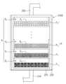
도 1은 고체 소스를 이용하여 공정을 수행하는 기판 처리 장치의 일 예를 보여주는 도면이다.
도 2는 캐니스터 내부, 즉, 반응 공간에서 일어나는 고체 소스의 상변화 반응을 개략적으로 보여주는 도면이다.
도 3a는 반응 공간을 구획화하는 일반적인 캐니스터의 일 예를 보여주는 도면이다.
도 3b는 도 3a의 캐니스터를 이용할 때, 시간에 따른 기체 소스의 공급양을 나타내는 도면이다.
도 3c는 도 3a의 캐니스터를 이용할 때, 시간에 따른 고체 소스들의 소모 시점을 보여주는 도면이다.
도 3d는 도 3a의 캐니스터의 등가 모델이다.
도 4는 본 발명의 일 실시예에 따른 캐니스터의 등가 모델이다.
도 5a는 도 4의 등가 모델을 구체화한 일 실시예에 따른 캐니스터를 보여주는 도면이다.
도 5b는 도 5a의 캐니스터를 이용할 때, 기체 소스의 공급양을 나타내는 도면이다.
도 5c는 도 5a의 캐니스터를 이용할 때, 시간에 따른 고체 소스들의 소모 시점을 보여주는 도면이다.
도 5d는 도 4의 등가 모델을 구체화한 일 실시예에 따른 캐니스터를 보여주는 도면이다.
도 6은 본 발명의 일 실시예에 따른 캐니스터의 등가 모델이다.
도 7a는 도 6의 등가 모델을 구체화한 일 실시예에 따른 캐니스터를 보여주는 도면이다.
도 7b는 도 6의 등가 모델을 구체화한 일 실시예에 따른 캐니스터를 보여주는 도면이다.
도 8은 본 발명의 일 실시예에 따른 캐니스터의 등가 모델이다.
도 9는 도 8의 등가 모델을 구체화한 일 실시예에 따른 캐니스터를 보여주는 도면이다.
도 10은 도 1의 기판 처리 장치를 이용하여 기판을 처리하는 과정을 도시하는 도면이다.
도 11a 및 도 11b는 기판 상에 박막을 증착하는 공정의 일 예를 보여주는 도면들이다.1 is a view showing an example of a substrate processing apparatus for performing a process using a solid source.
Figure 2 is a schematic representation of a phase change reaction of a solid source occurring in a canister, i. E., A reaction space.
FIG. 3A is a view showing an example of a general canister for partitioning a reaction space. FIG.
Fig. 3B is a diagram showing the supply amount of the gas source over time when the canister of Fig. 3A is used. Fig.
FIG. 3C is a view showing a consumption time point of solid sources over time when the canister of FIG. 3A is used. FIG.
Figure 3d is an equivalent model of the canister of Figure 3a.
4 is an equivalent model of a canister according to an embodiment of the present invention.
FIG. 5A is a view illustrating a canister according to an embodiment of the equivalent model of FIG.
5B is a view showing the supply amount of the gas source when the canister of Fig. 5A is used. Fig.
FIG. 5C is a view showing the consumption time of solid sources with time when using the canister of FIG. 5A. FIG.
5D is a view illustrating a canister according to an embodiment of the equivalent model of FIG.
6 is an equivalent model of a canister according to an embodiment of the present invention.
FIG. 7A is a view illustrating a canister according to an embodiment of the equivalent model of FIG. 6. FIG.
FIG. 7B is a view illustrating a canister according to an embodiment of the equivalent model of FIG. 6;
8 is an equivalent model of a canister according to an embodiment of the present invention.
FIG. 9 is a view illustrating a canister according to an embodiment of the equivalent model of FIG. 8;
10 is a view showing a process of processing a substrate using the substrate processing apparatus of FIG.
11A and 11B are views showing an example of a process of depositing a thin film on a substrate.
본 발명의 이점 및 특징, 그리고 그것들을 달성하는 방법은 첨부되는 도면과 함께 상세하게 후술되어 있는 실시예를 참조하면 명확해질 것이다. 그러나 본 발명은 이하에서 개시되는 실시예에 한정되는 것이 아니라 서로 다른 다양한 형태로 구현될 수 있으며, 단지 본 실시예는 본 발명의 개시가 완전하도록 하고, 본 발명이 속하는 기술분야에서 통상의 지식을 가진 자에게 발명의 범주를 완전하게 알려주기 위해 제공되는 것이며, 본 발명은 청구항의 범주에 의해 정의될 뿐이다. 명세서 전문에 걸쳐 동일 참조 부호는 동일 구성 요소를 지칭한다.BRIEF DESCRIPTION OF THE DRAWINGS The advantages and features of the present invention, and how to accomplish them, will become apparent by reference to the embodiments described in detail below with reference to the accompanying drawings. The present invention may, however, be embodied in many different forms and should not be construed as being limited to the embodiments set forth herein. Rather, these embodiments are provided so that this disclosure will be thorough and complete, and will fully convey the concept of the invention to those skilled in the art. Is provided to fully convey the scope of the invention to those skilled in the art, and the invention is only defined by the scope of the claims. Like reference numerals refer to like elements throughout the specification.
본 명세서에서 사용된 용어는 실시예들을 설명하기 위한 것이며 본 발명을 제한하고자 하는 것은 아니다. 본 명세서에서, 단수형은 문구에서 특별히 언급하지 않는 한 복수형도 포함한다. 명세서에서 사용되는 '포함한다(comprises)' 및/또는 '포함하는(comprising)'은 언급된 구성요소, 단계, 동작 및/또는 소자는 하나 이상의 다른 구성요소, 단계, 동작 및/또는 소자의 존재 또는 추가를 배제하지 않는다. 또한, 바람직한 실시예에 따른 것이기 때문에, 설명의 순서에 따라 제시되는 참조 부호는 그 순서에 반드시 한정되지는 않는다. The terminology used herein is for the purpose of illustrating embodiments and is not intended to be limiting of the present invention. In the present specification, the singular form includes plural forms unless otherwise specified in the specification. As used herein, the terms 'comprises' and / or 'comprising' mean that the stated element, step, operation and / or element does not imply the presence of one or more other elements, steps, operations and / Or additions. In addition, since they are in accordance with the preferred embodiment, the reference numerals presented in the order of description are not necessarily limited to the order.
또한, 본 명세서에서 기술하는 실시예들은 본 발명의 이상적인 예시도인 단면도 및/또는 평면도들을 참고하여 설명될 것이다. 도면들에 있어서, 막 및 영역들의 두께는 기술적 내용의 효과적인 설명을 위해 과장된 것이다. 따라서, 본 발명의 실시예들은 도시된 특정 형태로 제한되는 것이 아니라 제조 공정에 따라 생성되는 형태의 변화도 포함하는 것이다. In addition, the embodiments described herein will be described with reference to cross-sectional views and / or plan views, which are ideal illustrations of the present invention. In the drawings, the thicknesses of the films and regions are exaggerated for an effective description of the technical content. Accordingly, the embodiments of the present invention are not limited to the specific forms shown, but also include changes in the shapes that are generated according to the manufacturing process.
도 1은 고체 소스를 이용하여 공정을 수행하는 기판 처리 장치(1)의 일 예를 보여주는 도면이다. 기판 처리 장치(1)는 공정 챔버(100) 및 가스 공급 유닛(200)을 포함할 수 있다. 기판 처리 장치(1)는 고체 소스를 이용하여, 기판(10)에 대해 증착 공정을 수행할 수 있다. 일 예로, 기판 처리 장치(1)는 화학적 기상 증착(CVD: Chemical vapor deposition) 또는 원자층 기상 증착(ALD: Atomic layer deposition) 등과 같은 증착 장비일 수 있다. 그러나, 공정의 종류는 이에 제한되지 않고, 고체 소스를 이용하는 다양한 종류의 공정에 적용될 수 있다. 기판(10)은 웨이퍼일 수 있으나, 기판(10)의 종류는 이에 제한되지 않고, 다양한 종류의 기판에 적용 가능하다. 1 is a view showing an example of a
도 1을 참조하면, 공정 챔버(100)는 하우징(110), 지지부(120), 그리고 공정 가스 공급부(130)를 포함할 수 있다. 지지부(120)는 하우징(110) 내에 배치된다. 지지부(120) 상에 기판(10)이 안착되어, 기판(10)에 대해 공정을 진행할 수 있다. 공정 가스 공급부(130)는 지지부(120)의 상부(over)에, 지지부(120)와 대향되게 배치될 수 있다. 공정 가스 공급부(130)는 하우징(110)의 상면에 결합될 수 있다. 공정 가스 공급부(130)는 가스 공급 라인(250)으로부터 공정 가스를 공급받고, 지지부(120) 상의 기판(10)으로 이를 공급한다. 공정 가스 공급부(130)는 공정 가스 공급홀들(132)을 포함할 수 있다. 일 예로, 공정 가스 공급부(130)는 샤워 헤드(shower head)일 수 있다. Referring to FIG. 1, the
가스 공급 유닛(200)은, 고체 소스부(210), 캐리어 가스 공급부(240), 그리고 가스 공급 라인(250)을 포함할 수 있다. 고체 소스부(210)의 내부에는 고체 소스가 저장될 수 있다. 일 예로, 고체 소스는 HfCl4일 수 있다. 고체 소스부(210)는, 일 예로, 캐니스터(canister)일 수 있다. 이하, 고체 소스부(210)가 캐니스터(210)인 경우를 예로 들어 설명한다. 고체 소스의 개별 입자들은 파우더(powder) 형태이나, 고체 소스는 경화되어 소정의 부피를 가질 수 있다. The
캐리어 가스 공급부(240)는 캐니스터(210)에 연결될 수 있다. 캐리어 가스 공급부(240)는 캐니스터(210)로 캐리어 가스(carrier gas)를 공급한다. 캐리어 가스 공급부(240)는 캐리어 가스 공급원(242) 및 캐리어 가스 공급 라인(244)을 포함할 수 있다. 캐리어 가스는 고체 소스에 영향을 미치지 않도록 반응성이 작은 기체, 즉, 비활성 기체일 수 있다. 일 예로, 캐리어 가스는 질소 가스(N2)일 수 있으나, 이에 제한되지 않고, 캐리어 가스는 아르곤 가스(Ar) 또는 헬륨 가스(He) 등을 포함할 수 있다. 가스 공급 라인(250)은 캐니스터(210)와 공정 챔버(100)를 연결하고, 캐니스터(210)로부터 생성된 공정 가스를 공정 챔버(100)로 공급할 수 있다. 캐리어 가스 공급 라인(244) 및 가스 공급 라인(250)은 각각, 서로 대향되는 캐니스터(210)의 일면에 결합될 수 있으나, 이들의 결합 관계는 이에 제한되지 않는다. 예를 들어, 캐리어 가스 공급 라인(244) 및 가스 공급 라인(250)은 캐니스터(210)의 동일면에 결합될 수 있다. 도시되지 않았으나, 가스 공급 라인(250) 및 캐리어 가스 공급 라인(244) 상에는 개폐 밸브가 배치될 수 있다. 캐리어 가스 공급 라인(244) 및 가스 공급 라인(250) 각각은, 캐니스터(210)의 유입구 및 유출구와 대응될 수 있다. The carrier
도 2는 캐니스터(210) 내부, 즉, 반응 공간(R)에서 일어나는 고체 소스(A(s))의 상변화 반응을 개략적으로 보여주는 도면이다. 비록 도 2에는 반응 공간(R)이 캐리어 가스(C(g))가 제공되는 공간을 의미하는 것으로 도시되어 있으나, 반응 공간(R)은 캐리어 가스(C(g)) 및 고체 소스(A(s))가 공급되는 공간 모두를 의미한다. 도 2를 참조하면, 고체 소스(A(s))가 가열되어, 승화 반응이 일어난다. 캐리어 가스(C(g)) 및 고체 소스(A(s))가 서로 접촉하는 계면(I)에서, 고체 소스(A(s))가 승화되어 기체 소스(A(g))가 생성된다. 생성된 기체 소스(A(g))는 캐리어 가스(C(g))와 혼합될 수 있다. 이 때, 혼합된 생성된 기체 소스(A(g))와 캐리어 가스(C(g))를, 공정 챔버(100)로 공급되는 공정 가스로 정의한다. 캐리어 가스(C(g))는 기체 소스(A(g))를 운반할 뿐, 기체 소스(A(g))와 반응하지 않는다. 2 is a diagram schematically illustrating the phase change reaction of the solid source A (s) occurring in the
이 때, 승화 반응은 고체 소스(A(s))와 캐리어 가스(C(g))가 만나는 계면(I)에서 일어난다. 따라서, 계면(I)에서의 고체 소스(A(s)) 또는 캐리어 가스(C(g))의 반응 속도를 증가시키면, 고체 소스(A(s))의 승화 반응을 촉진할 수 있다. 예를 들어, 계면(I)의 표면적을 증가시키거나, 고체 소스(A(s))의 개별 입자들의 표면적을 증가시키는 경우, 승화 반응을 촉진할 수 있다. 반면, 고체 소스(A(s))가 담긴 깊이(D)를 증가시키는 경우, 고체 소스(A(s))의 전체 표면적은 증가되나 계면(I)의 표면적은 증가되지 않아, 반응 속도에는 영향을 미치지 않는다. 다시 말해서, 고체 소스(A(s))가 담긴 깊이(D)의 증가는 고체 소스(A(s))의 양의 증가와 대응될 뿐, 반응 속도 증가에는 기여하지 않는다. 이하, 계면(I)에서의 반응에 기여하는 표면적을 유효 표면적(E)으로 정의하고, 고체 소스(A(s))의 전체 표면적과 유효 표면적(E)을 구별한다. At this time, the sublimation reaction occurs at the interface I where the solid source A (s) and the carrier gas C (g) meet. Therefore, by increasing the reaction rate of the solid source A (s) or the carrier gas C (g) at the interface I, the sublimation reaction of the solid source A (s) can be promoted. For example, if the surface area of the interface I is increased or the surface area of the individual particles of the solid source A (s) is increased, the sublimation reaction can be promoted. On the other hand, when increasing the depth D of the solid source A (s), the total surface area of the solid source A (s) is increased but the surface area of the interface I is not increased, . In other words, an increase in the depth D of the solid source A (s) corresponds to an increase in the amount of the solid source A (s), but does not contribute to the increase in the reaction rate. Hereinafter, the surface area contributing to the reaction at the interface (I) is defined as the effective surface area (E), and the effective surface area (E) is distinguished from the total surface area of the solid source (A (s)).
효율적인 기체 소스(A(g))의 확보를 위해, 캐니스터(210) 내부에서의 상변화 반응을 촉진하는 다양한 방법이 사용될 수 있다. 일 예로, 캐니스터(210) 내부에서 고체 소스(A(s))의 유효 표면적(E)을 증가시키는 방법이 사용된다. 일 예로, 캐니스터(210)의 내부 공간을 분할 및 구획화하여, 고체 소스(A(s))의 유효 표면적(E)을 넓힐 수 있다. 캐니스터(210) 내에서, 캐리어 가스(C(g))는 일 방향(one-way)으로 흐를 수 있다. 즉, 캐니스터(210) 내에서, 캐리어 가스(C(g))는 비가역적인 흐름을 가진다. 캐니스터(210)로 유입되는 캐리어 가스의 흐름(flow)을 따라, 캐니스터(210)의 내부 공간을 구획화할 수 있다. Various methods of promoting the phase change reaction inside the
도 3a는 반응 공간을 구획화하는 일반적인 캐니스터(21)의 일 예를 보여주는 도면이다. 도 3a를 참조하면, 캐니스터(21)는 바디(220), 공간 분할부(P), 그리고 히터(230)를 포함할 수 있다. 바디(220)는 원통형일 수 있다. 이와 달리, 평면적 관점에서, 바디(220)는 다각형으로 제공될 수 있고, 바디(220)의 형태는 제한되지 않을 수 있다. 바디(220)는 내열성이 강하고 열 전도율이 높은 재질일 수 있다. 예를 들어, 바디(220)는 스테인레스를 포함할 수 있다. 히터(230)는 바디(220)를 감싸도록 제공된다. 히터(230)는, 일 예로, 히터 자켓(heater jacket)일 수 있으나, 이에 제한되지 않고, 코일 등을 포함할 수 있다. FIG. 3A is a view showing an example of a
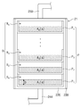
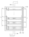
공간 분할부(P)가 배치되어, 내부 공간을 구획하고 반응 공간(R)을 정의할 수 있다. 공간 분할부(P)는 트레이(tray)일 수 있으나, 이에 제한되지 않는다. 공간 분할부(P)는 복수 개로 제공될 수 있고, 일 예로, 도 3a의 공간 분할부(P)는, 서로 등간격으로 배열된 n개의 서브 공간 분할부들(P1,P2,P3,…,Pn)을 포함할 수 있다. n개의 서브 공간 분할부들(P1,P2,P3,…,Pn)은 각각, n개의 서브 반응 공간들(R1,R2,R3,…,Rn)을 정의할 수 있다. 도 3a와 같이, 캐리어 가스 공급 라인(244)이 바디(220)의 하면에 연결되고, 가스 공급 라인(250)이 바디(220)의 상면에 연결되는 경우, 서브 공간 분할부들(P1,P2,P3,…,Pn)은 바디(220)의 높이 방향을 따라 배치될 수 있다. 각각의 서브 공간 분할부들(P1,P2,P3,…,Pn) 내에 담긴 고체 소스들(A1(s),A2(s),A3(s),…,An(s))은 서로 동일한 깊이(D) 및 유효 표면적(E)을 가지므로, 각각의 고체 소스들(A1,A2,A3,…,An)의 양은 서로 동일하다. The space partition P can be disposed to define the inner space and define the reaction space R. [ The space division P may be a tray, but is not limited thereto. 3A may be provided with a plurality of n subspace dividers P 1 , P 2 , P 3 , P 4 arranged at equal intervals from each other, ..., P n ). Each of the n subspace dividers P 1 , P 2 , P 3 , ..., P n may define n sub-reaction spaces R 1 , R 2 , R 3 , ..., R n . 3A, when the carrier
캐리어 가스 공급 라인(244)으로부터 공급된 캐리어 가스(C(g))는, 순차적으로 상단의 서브 반응 공간들로 이동할 수 있다. 캐리어 가스(C(g))는 상단의 서브 반응 공간들로 이동되면서, 각 반응 공간들(R1,R2,R3,…,Rn)에서 생성된 기체 소스들((A1(g),A2(g),A3(g),…,An(g)))를 함께 운반한다. 서브 반응 공간들(R1,R2,R3,…,Rn)을 거치면서 생성된 공정 가스는, 가스 공급 라인(250)으로 배출되어 공정 챔버(100)로 공급될 수 있다. 이와 같이, 캐니스터(210)의 내부 공간을 분할하여 복수의 서브 반응 공간들(R1,R2,R3,…,Rn)을 정의함으로써, 고체 소스(A(s))의 유효 표면적(E)을 넓히고 보다 많은 양의 기체 소스(A(g))를 얻을 수 있다. 서브 공간 분할부들(P1,P2,P3,…,Pn)에는 미세홀들(미도시)이 형성되어, 가스들의 흐름을 유도할 수 있다. 상술한 바와 같이, 고체 소스는 경화되어 제공될 수 있으므로, 미세홀들(미도시)에 의한 고체 소스의 손실은 발생하지 않는다. 이와 달리, 반응 공간(R)에는 가스 흐름을 유도하는 별도의 가스 흐름 경로(예를 들면, 유도관)가 배치될 수 있다. The carrier gas C (g) supplied from the carrier
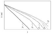
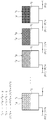
도 3b는 도 3a의 캐니스터(21)를 이용할 때, 시간에 따른 기체 소스(A(g))의 공급양(Flux rate)을 나타내는 도면이고, 도 3c는 도 3a의 캐니스터(21)를 이용할 때, 시간에 따른 고체 소스들의 소모 시점을 보여주는 도면이다. 도 3c는 도 3a의 캐니스터(21)가 5개의 서브 반응 공간들(R1,R2,R3,R4,R5) 및 5개의 고체 소스들(A1,A2,A3,A4,A5)을 포함하는 것을 예로 들어 도시한다. 도 3b를 참조하면, 시간이 지날수록 기체 소스(A(g))의 공급양(Flux rate)이 감소됨을 알 수 있다. 도 3c를 참조하면, 각 고체 소스들(A1,A2,A3,A4,A5)의 초기 깊이(D)는 동일하나, 고체 소스들(A1,A2,A3,A4,A5)간의 소모 시점이 서로 상이한 것을 알 수 있다. 캐리어 가스(C(g))의 흐름에 따라, 즉, 캐리어 가스(C(g))가 공급되는 순서에 따라, 고체 소스들(A1,A2,A3,A4,A5)이 순차적으로 소모된다. 기체 소스(A(g))의 공급양(Flux rate)의 감소 및 고체 소스들(A1,A2,A3,A4,A5)의 소모 시점들이 서로 상이한 이유를 이하 후술한다. FIG. 3B is a view showing the supply rate (flux rate) of the gas source A (g) with respect to time when the
도 3d는 도 3a의 캐니스터(21)의 등가 모델이다. 각각의 서브 반응 공간들(R1,R2,R3,…,Rn)에는, 서로 동일한 양의 고체 소스들(A1(s)=A2(s)=A3(s)=…=An(s))이 담긴다. 캐리어 가스(C(g))는 제 1, 제 2, 제 3, … 그리고 제 n 서브 반응 공간들(R1,R2,R3,…,Rn)에 순차적으로 공급된다. 이에 따라, 제 1, 제 2, 제 3, … 그리고 제 n 서브 반응 공간들(R1,R2,R3,…,Rn)에서 계속적으로 고체 소스들(A1(s),A2(s),A3(s),…,An(s))의 승화 반응이 진행되므로, 제 1, 제 2, 제 3, … 그리고 제 n 서브 반응 공간들(R1,R2,R3,…,Rn) 각각에서 배출되는 기체 소스들의 양이 점점 증가(A1(g)<A2(g)<A3(g)<…<An(g))한다. 반면에, 제 1, 제 2, 제 3, … 그리고 제 n 서브 반응 공간들(R1,R2,R3,…,Rn) 각각에서 배출되는 캐리어 가스들의 양은 점점 감소(C1(g)>C2(g)>C3(g)>…>Cn(g))한다. 따라서, 제 1, 제 2, 제 3, … 그리고 제 n 서브 반응 공간들(R1,R2,R3,…,Rn)로 갈수록 캐리어 가스의 상대 농도가 감소한다. 캐리어 가스의 농도 감소에 따라, 제 1, 제 2, 제 3, … 그리고 제 n 서브 반응 공간들(R1,R2,R3,…,Rn) 내의 고체 소스들(A1(s),A2(s),A3(s),…,An(s))의 반응 속도가 서로 상이해지고, 그에 따라, 제 1, 제 2, 제 3, … 그리고 제 n 서브 반응 공간들(R1,R2,R3,…,Rn) 내의 고체 소스들(A1(s),A2(s),A3(s),…,An(s))의 소모 시점이 서로 상이해진다. 이 때, 제 1, 제 2, 제 3, … 그리고 제 n 서브 반응 공간들(R1,R2,R3,…,Rn)의 각각에서 배출되는 캐리어 가스들(C1(g),C2(g),C3(g),…,Cn(g)) 및 기체 소스들(A1(s),A2(s),A3(s),…,An(s))은 설명의 편의를 위해 구분한 것일 뿐, 서로 동일한 가스를 의미한다. Figure 3d is an equivalent model of the
다시 말해서, 반응 공간들 내의 캐리어 가스의 농도 차이는 반응 속도의 차이를 야기하고, 반응 공간들에서의 반응 속도의 차이는 각 반응 공간들에 담긴 고체 소스들의 소진 시점 차이를 야기한다. 또한, 시간에 따라 불균일한 양의 기체 소스가 획득될 수 있다. 특히, 기체 소스 공급양의 감소는, 기판(10) 상에 형성되는 증착막의 두께를 감소시킬 수 있다. 따라서, 본 발명은 가스 흐름에 따라 전구체의 상대 농도 변화에 따른 반응 공간들간의 반응 속도 차이를 보상하여, 시간/가스의 흐름 또는 고체 소스의 충진양에 관계없이 일정한 양의 기체 소스(A(g))를 공급할 수 있는 캐니스터(210)를 제공하고자 한다. 이하, 도 2 및 도 3a를 참조하여 설명한 구성들과 실질적으로 동일한 구성에 대하여는 동일한 참조번호가 제공되고, 설명의 간소화를 위하여 중복되는 설명은 생략될 수 있다.In other words, the difference in the concentration of the carrier gas in the reaction spaces causes a difference in the reaction rate, and the difference in the reaction rates in the reaction spaces causes the difference in the exhaustion times of the solid sources contained in the respective reaction spaces. In addition, a non-uniform amount of gas source can be obtained over time. In particular, the reduction in the amount of the gas source supply can reduce the thickness of the evaporation film formed on the
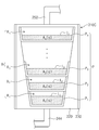
도 4는 본 발명의 일 실시예에 따른 캐니스터(210)의 등가 모델이다. 도 4를 참조하면, 서브 반응 공간들(R1,R2,R3,…,Rn)이 서로 상이한 양의 고체 소스를 포함(A1(s)>A2(s)>A3(s)>…>An(s))하는 것을 알 수 있다. 고체 소스들(A1(s),A2(s),A3(s),…,An(s))은 서로 다른 깊이(D1>D2>D3>…>Dn)를 가질 수 있다. 캐리어 가스(C(g))의 흐름에 따라, 제 1, 제 2, 제 3, …, 그리고 제 n 서브 반응 공간(R1,R2,R3,…,Rn)으로 갈수록 더 낮은 깊이(D1>D2>D3>…>Dn)를 가지므로, 제 1, 제 2, 제 3, …, 그리고 제 n 서브 반응 공간(R1,R2,R3,…,Rn)으로 갈수록 더 적은 양의 고체 소스(A1(s)>A2(s)>A3(s)>…>An(s))를 포함한다. 이 때, 제 1, 제 2, 제 3, …, 그리고 제 n 서브 반응 공간(R1,R2,R3,…,Rn) 각각에 담긴 고체 소스들의 양만이 상이할 뿐, 고체 소스들(A1(s),A2(s),A3(s),…,An(s))의 유효 표면적(E), 압력, 그리고 온도 등의 공정 조건들은 동일하게 제공된다. 도 3b 및 도 3c를 참조하여 확인한 바와 같이, 초기 반응 공간의 고체 소스가 후기 반응 공간의 고체 소스보다 빨리 소진되므로, 본 발명의 실시예에 따르면, 초기 반응 공간의 고체 소스의 양을 후기 반응 공간의 고체 소스의 양보다 많이 제공하여, 소모 시점을 보상할 수 있다. 즉, 반응 공간들은 가스 흐름에 따라 서로 다른 소모 속도를 갖지만, 각 반응 공간들에 담긴 고체 소스의 양을 제어하여 소모 시점을 동일하게 제어할 수 있다.4 is an equivalent model of the
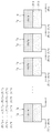
도 5a는 도 4의 등가 모델을 구체화한 일 실시예에 따른 캐니스터(210A)를 보여주는 도면이다. 캐니스터(210A)는 바디(220), 공간 분할부(P), 그리고 히터(230)를 포함할 수 있다. 캐리어 가스 공급 라인(244)과 가스 공급 라인(250)은 캐니스터(210C)의 서로 대향되는 면에 연결될 수 있다. 보다 구체적으로, 도 5a의 캐니스터(210A)의 하면에 캐리어 가스 공급 라인(244)이 결합되고 상면에 가스 공급 라인(250)이 결합되어, 하부에서부터 상부를 향하는 가스 흐름을 가질 수 있다. 따라서, 공간 분할부(P)는 바디(220)의 높이 방향을 따라 배치된 제 1, 제 2, 제 3, …, 그리고 제 n 서브 공간 분할부들(P1,P2,P3,…,Pn)을 포함할 수 있다. 제 1, 제 2, 제 3, …, 그리고 제 n 서브 공간 분할부들(P1,P2,P3,…,Pn) 각각에 담긴 고체 소스들의 깊이(D1>D2>D3>…>Dn)는 점점 감소될 수 있다. 다시 말해서, 제 1, 제 2, 제 3, …, 그리고 제 n 서브 공간 분할부들(P1,P2,P3,…,Pn) 각각에 담긴 고체 소스들의 양은 점점 감소(A1(s)>A2(s)>A3(s)>…>An(s))될 수 있다. 이와 대응되도록, 제 1, 제 2, 제 3, …, 그리고 제 n 서브 공간 분할부들(P1,P2,P3,…,Pn)은 바디(220)의 상부로 갈수록, 낮은 높이를 가질 수 있으나, 이에 제한되지 않는다. FIG. 5A is a view illustrating a
도 5b는 도 5a의 캐니스터(210A)를 이용할 때, 기체 소스(A(g))의 공급양(Flux rate)을 나타내는 도면이고, 도 5c는 도 5a의 한 통의 캐니스터(210A)를 이용할 때, 시간에 따른 고체 소스들의 소모 시점을 보여주는 도면이다. 도 5c는 도 5a의 캐니스터(210A)가 5개의 서브 반응 공간들(R1,R2,R3,R4,R5) 및 5개의 고체 소스들(A1,A2,A3,A4,A5)을 포함하는 것을 예로 들어 도시한다. 도 3b 및 도 5b를 비교하면, 시간에 따라 획득되는 기체 가스(A(g))의 공급량이 균일해진 것을 알 수 있다. 또한, 도 3c 및 도 5c를 비교하면, 캐니스터(210A)의 고체 소스들의 초기 깊이를 서로 상이(D1>D2>D3>…>Dn)하게 함으로써, 고체 소스들(A1,A2,A3,A4,A5) 간의 소모 시점이 서로 유사한 것을 알 수 있다. 즉, 고체 소스들(A1,A2,A3,A4,A5)의 소모 시점을 동일하게 제어하여, 시간에 따라 균일한 양의 기체 소스(A(g))를 획득할 수 있다. 5B is a view showing the supply rate of the gas source A (g) when the
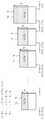
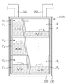
도 5d는 도 4의 등가 모델을 구체화한 일 실시예에 따른 캐니스터(210B)를 보여주는 도면이다. 캐리어 가스 공급 라인(244)과 가스 공급 라인(250)은 캐니스터(210)의 동일면 상에 연결될 수 있다. 이에 따라, 캐니스터(210B) 내에서, 캐리어 가스는 일측에서 유입되어 다시 일측으로 유출되는 가스 흐름을 가질 수 있다. 일 예로, 도 5d의 캐니스터(210B)는 상부에서부터 유입되어 내부를 흐른 뒤에 다시 상부로 유출되는 가스 흐름을 갖는다. 따라서, 가스 흐름을 따라 배치된 제 1, 제 2, 제 3, …, 그리고 제 n 서브 공간 분할부들(P1,P2,P3,P4,P5,…,Pn)을 포함할 수 있다. 즉, 도 5a의 캐니스터(210A)는 바디(220) 내의 반응 공간(R)이 수직하게 분할된 구조만을 도시하나, 도 5d의 캐니스터(210B)는 수직 및 수평으로 분할된 공간들을 갖는다. 서브 공간 분할부들(P1,P2,P3,P4,P5,…,Pn) 각각에 담긴 고체 소스들의 깊이들은 점점 감소(D1>D2>D3>D4>D5>…>Dn)될 수 있다. 다시 말해서, 서브 공간 분할부들(P1,P2,P3,P4,P5,…,Pn) 각각에 담긴 고체 소스들의 양은 점점 감소(A1(s)>A2(s)>A3(s)>A4(s)>A5(s)>…>An(s))될 수 있다. FIG. 5D is a view illustrating a
도 4 내지 도 5d를 참조하여 설명한 캐니스터들(210A,210B)의 구조들은, 캐리어 가스의 흐름에 따라 서로 상이한 양의 고체 소스를 포함할 수 있다. 보다 구체적으로, 초기에 배치된 반응 공간 내의 고체 소스의 양은 후기에 배치된 반응 공간 내의 그것보다 많다. 이 때, 고체 소스의 양들의 차이에 따른 효과를 설명하기 위해, 본 발명에서는 고체 소스들의 깊이(D)를 비교하여 설명하였으나, 이는 유효 표면적(E)을 동일하게 제어하여 비교 설명하기 위한 예시일 뿐, 고체 소스의 양을 제어하는 방법은 이에 제한되지 않는다. 또한, 캐니스터 내부의 공간 분할 방식 및 분할된 공간의 수 등은 제한되지 않는다. 또한, 각 반응 공간들에 담긴 고체 소스들의 양의 차이는 연속적일 수 있으나, 이와 달리, 비연속적일 수 있다.The structures of the
도 6은 본 발명의 일 실시예에 따른 캐니스터(210)의 등가 모델이다. 도 6을 참조하면, 캐리어 가스(C(g))의 흐름에 따라, 서브 반응 공간들(R1,R2,R3,…,Rn)이 더 넓은 계면(I1<I2<I3<…<In)을 가질 수 있다. 이에 따라, 제 1, 제 2, 제 3, …, 그리고 제 n 서브 반응 공간들(R1,R2,R3,…,Rn)의 유효 표면적이 점점 증가(E1<E2<E3<…<En)할 수 있다. 고체 소스(A(s))와 캐리어 가스가 접촉하는 계면(I)에서 고체 소스(A(s))의 승화가 일어나므로, 계면(I)의 면적을 증가시켜 더 많은 기체 소스(A(g))를 획득할 수 있다. 이 때, 서브 반응 공간들(R1,R2,R3,…,Rn) 각각의 고체 소스의 양, 압력, 그리고 온도 등의 공정 조건들은 동일하게 제공된다. Figure 6 is an equivalent model of the
제 1, 제 2, 제 3, …, 그리고 제 n 서브 반응 공간으로 갈수록 더 큰 계면들, 즉, 더 큰 유효 표면적을 가질 수 있으므로(E1<E2<E3<…<En), 제 1, 제 2, 제 3, …, 그리고 제 n 서브 반응 공간으로 갈수록 더 많은 양의 기체 소스를 획득(A1(g)<A2(g)<A3(g)<…<An(g))할 수 있다. 따라서, 후기 반응 공간의 계면의 유효 표면적을 초기 반응 공간의 계면의 그것보다 크게 제공하여, 반응 공간들 간의 반응 속도 차이를 보상할 수 있다. 즉, 도 3c를 참조하면, 초기 반응 공간의 반응 속도에 비해 후기 반응 공간의 반응 속도가 작으나, 초기 반응 공간의 반응 속도에 비해 후기 반응 공간의 반응 속도를 증가시킴으로써, 반응 공간들 간의 반응 속도 차이를 보상할 수 있다. 반응 속도를 실질적으로 균일하게 제어하는 경우, 각 반응 공간들의 소모 시점 또한 동일하게 제어할 수 있으므로, 시간에 따라 획득되는 기체 가스 공급양의 감소를 보상할 수 있다.The first, second, third, ... (E 1 <E 2 <E 3 <... <E n ), the first, second, third, ..., and so on, can have larger interfaces , And it is able to obtain the n-th sub-larger amount of source gas toward the reaction space (A 1 (g) <A 2 (g) <A 3 (g) <... <A n (g)). Accordingly, the effective surface area of the interface of the later reaction space can be made larger than that of the interface of the initial reaction space, so that the difference in reaction rate between reaction spaces can be compensated. That is, referring to FIG. 3C, although the reaction rate of the latter reaction space is smaller than the reaction rate of the initial reaction space, by increasing the reaction rate of the latter reaction space relative to the reaction rate of the initial reaction space, Can be compensated. When the reaction rate is controlled substantially uniformly, the consumption points of the respective reaction spaces can be controlled at the same time, so that it is possible to compensate for the reduction in the gas gas supply amount obtained over time.
도 7a는 도 6의 등가 모델을 구체화한 일 실시예에 따른 캐니스터(210C)를 보여주는 도면이다. 캐니스터(210C)는 바디(220), 공간 분할부(P), 그리고 히터(230)를 포함할 수 있다. 캐리어 가스 공급 라인(244)과 가스 공급 라인(250)은 캐니스터(210C)의 서로 대향되는 면에 연결될 수 있다. 보다 구체적으로, 도 7a의 캐니스터(210C)의 하면에 캐리어 가스 공급 라인(244)이 결합되고 상면에 가스 공급 라인(250)이 결합되어, 하부에서부터 상부를 향하는 가스 흐름을 가질 수 있다. 따라서, 공간 분할부(P)는 바디(220)의 높이 방향을 따라 배치된 제 1, 제 2, 제 3, …, 그리고 제 n 서브 공간 분할부들(P1,P2,P3,…,Pn)을 포함할 수 있다. 제 1, 제 2, 제 3, …, 그리고 제 n 서브 공간 분할부들(P1,P2,P3,…,Pn)은 바디(220)의 상부로 갈수록 증가된 폭, 즉, 넓은 계면(I1<I2<I3<…<In)을 가질 수 있다. 제 1, 제 2, 제 3, …, 그리고 제 n 서브 공간 분할부들(P1,P2,P3,…,Pn)이 점차 증가된 계면(I1<I2<I3<…<In)을 가지므로, 제 1, 제 2, 제 3, …, 그리고 제 n 서브 공간 분할부들(P1,P2,P3,…,Pn) 내에 담긴 고체 소스들의 유효 표면적 또한 증가(E1<E2<E3<…<En)될 수 있다. 서브 공간 분할부들(P1,P2,P3,…,Pn) 각각에 담긴 고체 소스들의 양은 서로 동일(A1(s)=A2(s)=A3(s)=…=An(s))하다.FIG. 7A is a view illustrating a
도 7b는 도 6의 등가 모델을 구체화한 일 실시예에 따른 캐니스터(210D)를 보여주는 도면이다. 캐리어 가스 공급 라인(244)과 가스 공급 라인(250)은 캐니스터(210D)의 동일면 상에 연결될 수 있다. 캐니스터(210D) 내의 캐리어 가스는, 일측에서 유입되어 다시 일측으로 유출되는 가스 흐름을 가질 수 있다. 일 예로, 도 7b의 캐니스터(210D)는 상부에서부터 유입되어 내부를 흐른 뒤에 다시 상부로 유출되는 가스 흐름을 갖는다. 따라서, 공간 분할부(P)는 가스 흐름을 따라 배치된 제 1, 제 2, 제 3, …, 그리고 제 n 서브 공간 분할부들(P1,P2,P3,P4,…,Pn)을 포함할 수 있다. 즉, 도 7a의 캐니스터(210C)는 바디(220) 내의 반응 공간(R)이 수직하게 분할된 구조만을 도시하나, 도 7b의 캐니스터(210D)는 수직 및 수평으로 분할된 공간들을 갖는다. 제 1, 제 2, 제 3, …, 그리고 제 n 서브 공간 분할부들(P1,P2,P3,P4,…,Pn) 각각에 담긴 고체 소스들의 계면의 표면적은 점점 증가(I1<I2<I3<I4<…<In)될 수 있다. 다시 말해서, 제 1, 제 2, 제 3, …, 그리고 제 n 서브 공간 분할부들(P1,P2,P3,P4,…,Pn) 각각에 담긴 고체 소스들의 유효 표면적은 점점 증가(E1<E2<E3<E4<…<En)될 수 있다. 서브 공간 분할부들(P1,P2,P3,P4,…,Pn) 각각에 담긴 고체 소스들의 양은 서로 동일(A1(s)=A2(s)=A3(s)=…=An(s))하다.FIG. 7B is a view illustrating a
도 6 내지 도 7b를 참조하여 설명한 캐니스터들(210C,210D)의 구조들은, 캐리어 가스의 흐름에 따라 서로 상이한 유효 표면적을 갖는 고체 소스들을 포함할 수 있다. 보다 구체적으로, 초기에 배치된 반응 공간의 계면의 표면적보다 후기에 배치된 반응 공간의 계면의 표면적이 크다. 이 때, 계면의 표면적의 차이에 따른 효과를 설명하기 위해, 본 발명에서는 각 고체 소스들이 동일한 양으로 제공되는 것을 예로 들어 설명하였으나, 이에 제한되지 않는다. 또한, 캐니스터 내부의 공간 분할 방식 및 분할된 공간의 수 등은 제한되지 않는다. 또한, 각 반응 공간들의 계면의 표면적의 차이는 연속적일 수 있으나, 이와 달리, 비연속적일 수 있다.The structures of the
도 8은 본 발명의 일 실시예에 따른 캐니스터(210)의 등가 모델이다. 도 8을 참조하면, 캐리어 가스(C(g))의 흐름에 따라, 서브 반응 공간들(R1,R2,R3,…,Rn)이 서로 상이한 유효 표면적을 가질 수 있다. 보다 구체적으로, 제 1, 제 2, 제 3, …, 그리고 제 n 서브 반응 공간(R1,R2,R3,…,Rn)으로 갈수록, 제 1, 제 2, 제 3, …, 그리고 제 n 고체 소스들의 개별 입자들은 더 큰 입자 크기(S1<S2<S3<…<Sn)를 가질 수 있다. 이에 따라, 제 1, 제 2, 제 3, …, 그리고 제 n 서브 반응 공간들(R1,R2,R3,…,Rn)의 유효 표면적이 점점 증가(E1<E2<E3<…<En)할 수 있다. 즉, 고체 소스 입자 자체의 표면적을 증가시켜, 고체 소스 입자의 반응 속도를 증가시킬 수 있다. 이 때, 서브 반응 공간들(R1,R2,R3,…,Rn) 각각의 고체 소스의 양, 압력, 그리고 온도 등의 공정 조건들은 동일하게 제공된다. 8 is an equivalent model of the
제 1, 제 2, 제 3, …, 그리고 제 n 서브 반응 공간으로 갈수록 더 큰 입자 크기, 즉, 더 큰 유효 표면적을 가질 수 있으므로(E1<E2<E3<…<En), 제 1, 제 2, 제 3, …, 그리고 제 n 서브 반응 공간으로 갈수록 더 많은 양의 기체 소스를 획득(A1(g)<A2(g)<A3(g)<…<An(g))할 수 있다. 따라서, 후기 반응 공간의 고체 소스의 입자 크기를 초기 반응 공간의 그것보다 크게 제공하여, 반응 공간들 간의 반응 속도 차이를 보상할 수 있다. 즉, 도 3c를 참조하면, 초기 반응 공간의 반응 속도에 비해 후기 반응 공간의 반응 속도가 작으나, 초기 반응 공간의 반응 속도에 비해 후기 반응 공간의 반응 속도를 증가시킴으로써, 반응 공간들 간의 반응 속도 차이를 보상할 수 있다. 반응 속도를 실질적으로 균일하게 제어하는 경우, 각 반응 공간들 내의 고체 소스들의 소모 시점 또한 동일하게 제어할 수 있으므로, 시간에 따라 획득되는 기체 가스 공급양의 감소를 보상할 수 있다.The first, second, third, ... (E 1 <E 2 <E 3 <... <E n ), and the first, second, third, ..., and n-th sub reaction spaces , And it is able to obtain the n-th sub-larger amount of source gas toward the reaction space (A 1 (g) <A 2 (g) <A 3 (g) <... <A n (g)). Thus, the particle size of the solid source of the latter reaction space can be made larger than that of the initial reaction space, so that the difference in reaction rate between reaction spaces can be compensated. That is, referring to FIG. 3C, although the reaction rate of the latter reaction space is smaller than the reaction rate of the initial reaction space, by increasing the reaction rate of the latter reaction space relative to the reaction rate of the initial reaction space, Can be compensated. When the reaction rate is controlled to be substantially uniform, the consumption points of the solid sources in the respective reaction spaces can be controlled equally, so that the reduction of the gaseous gas supply amount obtained over time can be compensated.
도 9는 도 8의 등가 모델을 구체화한 일 실시예에 따른 캐니스터(210E)를 보여주는 도면이다. 캐니스터(210E)는 바디(220), 공간 분할부(P), 그리고 히터(230)를 포함할 수 있다. 캐리어 가스 공급 라인(244)과 가스 공급 라인(250)은 캐니스터(210E)의 서로 대향되는 면에 연결될 수 있다. 보다 구체적으로, 도 9의 캐니스터(210E)의 하면에 캐리어 가스 공급 라인(244)이 결합되고 상면에 가스 공급 라인(250)이 결합되어, 하부에서부터 상부를 향하는 가스 흐름을 가질 수 있다. 따라서, 공간 분할부(P)는 바디(220)의 높이 방향을 따라 배치된 제 1, 제 2, 제 3, …, 그리고 제 n 서브 공간 분할부들(P1,P2,P3,…,Pn)을 포함할 수 있다. 제 1, 제 2, 제 3, …, 그리고 제 n 공간 분할부들(P1,P2,P3,…,Pn) 각각에 담긴 고체 소스들의 입자 크기는 점점 증가(S1<S2<S3<…<Sn)될 수 있다. 고체 소스들의 입자 크기들이 점점 증가(S1<S2<S3<…<Sn)되므로, 제 1, 제 2, 제 3, …, 그리고 제 n 서브 공간 분할부들(P1,P2,P3,…,Pn) 내에 담긴 고체 소스들의 유효 표면적 또한 증가(E1<E2<E3<…<En)될 수 있다. 서브 공간 분할부들(P1,P2,P3,…,Pn) 각각에 담긴 고체 소스들의 양은 서로 동일(A1(s)=A2(s)=A3(s)=…=An(s))하다.FIG. 9 is a view showing a
도 8 내지 도 9를 참조하여 설명한 캐니스터들(210E)의 구조는, 캐리어 가스의 흐름에 따라 서로 상이한 유효 표면적을 갖는 고체 소스들을 포함할 수 있다. 보다 구체적으로, 초기에 배치된 고체 소스들의 개별 입자 크기보다 후기에 배치된 고체 소스들의 개별 입자 크기가 크다. 이 때, 각 입자 크기에 따른 효과를 설명하기 위해, 본 발명에서는 각 고체 소스들이 동일한 양으로 제공되는 것을 예로 들어 설명하였으나, 이에 제한되지 않는다. 또한, 캐니스터 내부의 공간 분할 방식 및 분할된 공간의 수 등은 제한되지 않는다. 또한, 각 고체 소스들의 개별 입자 크기의 차이는 연속적일 수 있으나, 이와 달리, 비연속적일 수 있다.The structure of the
상술한 실시예들은 각각, 반응 공간 내에서 가스 흐름에 따라, 서로 다른 고체 소스의 충진양, 승화 공정이 진행되는 계면의 표면적, 또는 개별 입자의 크기 중 적어도 어느 하나를 갖는 것을 예로 들어 설명하였다. 그러나, 이는 설명의 편의를 위한 것이며, 이들의 다양한 조합이 가능함은 것은 자명하다. Each of the above-described embodiments has been described by taking as an example the fact that depending on the gas flow in the reaction space, the filling amount of different solid sources, the surface area of the interface at which the sublimation process proceeds, or the size of individual particles. However, it is for convenience of explanation, and it is apparent that various combinations of these are possible.
도 10은 도 1의 기판 처리 장치(1)를 이용하여 기판을 처리하는 과정을 도시하는 도면이다. 이 때, 도 1의 캐니스터(210)는 상술한 캐니스터들(210A,210B,210C,210D,210E) 중 어느 하나일 수 있다. 도 1 및 도 10을 참조하여 기판 처리 방법을 설명하면, 고체 소스를 이용하여 기판(10) 상에 공정 가스를 공급(S100)하고, 공정 가스를 이용하여 기판(10)을 처리한다(S200). 일 예로, 기판(10) 상에 박막을 증착하는 공정일 수 있다. 이 때, 고체 소스를 이용하여 기판(10) 상에 공정 가스를 공급하는 것을 구체화하면, 먼저, 캐니스터(210)의 반응 공간 내에서 고체 소스가 승화되어 기체 소스가 생성된다(S110). 반응 공간 내에 일 방향(one-way)을 따라 캐리어 가스를 주입(S120)하면, 캐리어 가스가 기체 소스를 함께 운반하여, 캐리어 가스 및 기체 소스가 혼합된 공정 가스를 공정 챔버(100)로 공급할 수 있다(S130). 이 때, 캐니스터(210) 내에서 가스들이 비가역적인 일 방향의 흐름을 갖고, 일 방향에 따라 반응 속도 차이가 발생한다. 보다 구체적으로, 반응 공간 내에서 가스들의 흐름에 따라, 초기의 반응 속도가 후기의 반응 속도보다 빠르게 되어, 초기에 제공된 고체 소스가 후기에 제공된 고체 소스에 비해 먼저 소진될 수 있다. 본 발명의 실시예들에 따르면, 반응 속도 차이를 보상할 수 있다(S140). 10 is a view showing a process of processing a substrate by using the
먼저, 반응 공간 내 담긴 고체 소스의 양을 조절하여 반응 속도 차이를 보상할 수 있다(S142). 보다 구체적으로, 초기의 반응 속도가 후기의 반응 속도보다 빨라 초기에 제공된 고체 소스가 후기에 제공된 고체 소스에 비해 먼저 소진되므로, 초기에 제공하는 고체 소스의 양을 후기에 제공하는 그것보다 많도록 제어하여 소모 시점들을 일치시킬 수 있다. First, the reaction rate difference can be compensated by adjusting the amount of the solid source contained in the reaction space (S142). More specifically, since the initial reaction rate is faster than the later reaction rate, the initially provided solid source is exhausted earlier than the later provided solid source, so that the amount of the initially provided solid source is controlled more than that provided later So that consumption points can be matched.
또한, 반응 공간 내의 고체 소스의 반응 속도 자체를 조절할 수 있다(S144). 보다 구체적으로, 초기의 반응 속도가 후기의 반응 속도보다 빠르므로, 초기의 반응 속도를 감소시키거나 후기의 반응 속도를 감소시켜, 반응 속도들이 서로 동일하도록 제어할 수 있다. 일 예로, 고체 소스의 유효 표면적을 조절할 수 있다(S146). 예를 들어, 고체 소스의 상변화 반응이 진행되는 계면의 표면적을 조절(S147)하거나, 고체 소스의 개별 입자 크기를 조절(S148)할 수 있다. Further, the reaction rate itself of the solid source in the reaction space can be controlled (S144). More specifically, since the initial reaction rate is faster than the latter reaction rate, it is possible to control the reaction rates to be the same by decreasing the initial reaction rate or reducing the reaction rate in the latter period. As an example, the effective surface area of the solid source can be adjusted (S146). For example, the surface area of the interface at which the phase change reaction of the solid source proceeds can be controlled (S147) or the individual particle size of the solid source can be adjusted (S148).
도 11a 및 도 11b는 기판(310) 상에 박막을 증착하는 공정의 일 예를 보여주는 도면들이다. 도 11a를 참조하면, 기판(310) 상에 제1 반도체 패턴(SP1) 및 제2 반도체 패턴(SP2)을 포함하는 상부 반도체 패턴(USP)이 형성되고, 상부 반도체 패턴(USP) 및 하부 반도체 패턴(LSP)을 포함하는 수직 반도체 패턴(VSP)이 형성될 수 있다. FIGS. 11A and 11B are views showing an example of a process of depositing a thin film on the
보다 구체적으로, 버퍼 유전막(332) 상에 희생막들(미도시) 및 절연막들(335)을 교대로 그리고 반복적으로 형성하고, 희생막들(미도시) 및 절연막들(335)을 관통하는 수직 홀들(VH)을 형성할 수 있다. 수직 홀들(VH)의 각각의 하부를 채우는 하부 반도체 패턴(LSP)을 형성하고, 이어서, 정보 저장 구조체(340), 제1 반도체 패턴(SP1), 제2 반도체 패턴(SP2) 및 매립 절연체(342)를 순차적으로 형성할 수 있다. 이후, 절연막들(335), 희생막들(미도시), 및 버퍼 유전막(332)을 연속적으로 패터닝하여 분리 트렌치들(T)을 형성하면, 분리 트렌치들(T)에 의해 노출된 희생막들(미도시)을 선택적으로 제거하여 게이트 영역(334)을 형성할 수 있다. More specifically, sacrificial films (not shown) and insulating
도 11b를 참조하면, 게이트 영역(334)에 의해 노출된 하부 반도체 패턴(LSP)을 열산화하여 게이트 산화막(GOX)을 형성하고, 게이트 영역(334)에 의해 노출된 절연막들(335) 및 정보 저장 구조체(340) 상에 절연 패턴들(337)을 형성할 수 있다. 이 때, 절연 패턴들(337)을 형성하는 것은 원자층 증착(ALD) 공정을 수행하는 것을 포함할 수 있다. 즉, 본 발명의 기판 처리 장치(1)를 이용하여, 고체 소스인 HfCl4를 이용하여 절연 패턴들(337)을 형성할 수 있다. 절연 패턴들(337)은 실리콘 산화막 또는 고유전막(일 예로, 알루미늄 산화막 또는 하프늄 산화막)을 포함할 수 있다. 11B, the lower semiconductor pattern LSP exposed by the
이후에, 분리 트렌치들(T)을 통하여, 게이트 영역(334) 내에 도전막(미도시)이 형성될 수 있다. 도전막을 형성하는 것은 원자층 증착(ALD) 공정을 수행하는 것을 포함할 수 있다. 즉, 본 발명의 기판 처리 장치(1)를 이용하여, 고체 소스인 WClx를 이용하여 도전막(미도시)을 형성할 수 있다. 이어서, 게이트 영역(334)의 외부(즉, 분리 트렌치들(T))에 형성된 도전막(미도시)을 제거하여, 게이트 영역(334)의 내에 전극들(330)을 형성할 수 있다. 전극들(330), 버퍼 유전막(332), 절연막들(335), 및 절연 패턴들(337)을 포함하는 적층 구조체들(ST)이 정의될 수 있다. 전극들(330)은 배치 관계에 따라 각각, 접지 선택 라인(GSL), 워드 라인들(WL), 그리고 스트링 선택 라인들(SSL)으로 기능할 수 있다.Thereafter, a conductive film (not shown) may be formed in the
본 발명의 실시예에 따르면, 공정 진행 및 시간 흐름에 상관없이 균일한 공정 가스를 공급할 수 있다. 본 발명은 고체 소스를 이용하는 다양한 공정에 적용될 수 있고, 고체 소스 또한 PDMAT, HfCl4, WClx 등 다양한 종류에 적용 가능하다.According to the embodiment of the present invention, a uniform process gas can be supplied regardless of process progress and time flow. The present invention can be applied to various processes using a solid source, and the solid source can also be applied to various types such as PDMAT, HfCl4, WClx, and the like.
이상의 실시 예들은 본 발명의 이해를 돕기 위하여 제시된 것으로, 본 발명의 범위를 제한하지 않으며, 이로부터 다양한 변형 가능한 실시 예들도 본 발명의 범위에 속하는 것임을 이해하여야 한다. 본 발명의 기술적 보호범위는 특허청구범위의 기술적 사상에 의해 정해져야 할 것이며, 본 발명의 기술적 보호범위는 특허청구범위의 문언적 기재 그 자체로 한정되는 것이 아니라 실질적으로는 기술적 가치가 균등한 범주의 발명에 대하여까지 미치는 것임을 이해하여야 한다.It is to be understood that the above-described embodiments are provided to facilitate understanding of the present invention, and do not limit the scope of the present invention, and it is to be understood that various modifications are possible within the scope of the present invention. It is to be understood that the technical scope of the present invention should be determined by the technical idea of the claims and the technical scope of protection of the present invention is not limited to the literary description of the claims, To the invention of the invention.
Claims (20)
상기 반응 공간을 복수의 서브 반응 공간들로 분할하는 공간 분할부;
상기 바디의 일측에 형성되고, 캐리어 가스가 유입되는 유입구; 및
상기 바디의 타측에 형성되고, 상기 캐리어 가스 및 상기 기체 소스가 배출되는 유출구를 포함하되,
상기 분할된 상기 복수의 서브 반응 공간들 중 상기 유입구와 인접한 서브 반응 공간과 상기 유출구와 인접한 서브 반응 공간은, 상기 고체 소스의 양 및 상기 고체 소스의 유효 표면적 중 적어도 어느 하나가 서로 상이한, 고체 소스 공급 유닛.
A body provided with a solid source and having a reaction space in which the solid source sublimates to produce a gaseous source;
A space dividing unit dividing the reaction space into a plurality of sub reaction spaces;
An inlet formed at one side of the body and through which the carrier gas flows; And
And an outlet formed on the other side of the body for discharging the carrier gas and the gas source,
Wherein a sub-reaction space adjacent to the inlet and a sub-reaction space adjacent to the outlet of the plurality of divided sub-reaction spaces are formed in a solid source, wherein at least one of the amount of the solid source and the effective surface area of the solid source is different from each other, Supply unit.
상기 유입구와 인접한 서브 반응 공간 내의 고체 소스의 양은 상기 유출구와 인접한 서브 반응 공간 내의 고체 소스의 양보다 많은, 고체 소스 공급 유닛.
The method according to claim 1,
Wherein the amount of solid source in the sub-reaction space adjacent the inlet is greater than the amount of solid source in the sub-reaction space adjacent the outlet.
상기 유효 표면적은 상기 고체 소스의 승화에 기여하는 표면적이되,
상기 유출구와 인접한 서브 반응 공간의 유효 표면적은 상기 유입구와 인접한 서브 반응 공간의 고체 소스의 유효 표면적보다 큰, 고체 소스 공급 유닛.
The method according to claim 1,
The effective surface area is a surface area that contributes to the sublimation of the solid source,
Wherein the effective surface area of the sub-reaction space adjacent the outlet is greater than the effective surface area of the solid source of the sub-reaction space adjacent the inlet.
상기 유효 표면적은, 상기 고체 소스와 상기 캐리어 가스가 접촉하는 계면의 표면적을 포함하는, 고체 소스 공급 유닛.
The method of claim 3,
Wherein the effective surface area comprises a surface area of the interface at which the solid source and the carrier gas contact.
상기 유효 표면적은, 상기 고체 소스의 개별 입자의 표면적을 포함하는, 고체 소스 공급 유닛.
5. The method of claim 4,
Wherein the effective surface area comprises a surface area of individual particles of the solid source.
상기 바디를 가열하는 히터를 더 포함하는, 고체 소스 공급 유닛.
The method according to claim 1,
And a heater for heating the body.
상기 고체 소스부로 캐리어 가스를 공급하는 캐리어 가스 공급부; 및
상기 고체 소스부와 외부를 연결하고, 상기 고체 소스부 내에서 생성된 기체 소스와 상기 캐리어 가스를 상기 외부로 공급하는 가스 공급 라인을 포함하되,
상기 고체 소스부는:
상기 고체 소스를 각각 포함하는 복수 개의 반응 공간들을 갖되,
상기 반응 공간들 중 상기 캐리어 가스 공급부와 인접하는 반응 공간 내의 고체 소스의 양은, 상기 반응 공간들 중 상기 가스 공급 라인과 인접하는 반응 공간 내의 그것보다 많은, 가스 공급 유닛.
A solid source portion comprising a solid source;
A carrier gas supply unit for supplying a carrier gas to the solid source unit; And
And a gas supply line which connects the solid source part and the outside and supplies a gas source generated in the solid source part and the carrier gas to the outside,
The solid source portion comprises:
A plurality of reaction spaces each containing the solid source,
Wherein the amount of the solid source in the reaction space adjacent to the carrier gas supply part of the reaction spaces is larger than that in the reaction space adjacent to the gas supply line among the reaction spaces.
상기 고체 소스부는, 상기 복수 개의 반응 공간들을 구획화하는 상기 복수 개의 공간 분할부를 더 포함하는, 가스 공급 유닛.
8. The method of claim 7,
Wherein the solid source portion further comprises the plurality of space dividing portions for dividing the plurality of reaction spaces.
상기 고체 소스부 내에서 상기 캐리어 가스는 일 방향(one-way)으로 이동하고,
상기 복수 개의 반응 공간들은 상기 일 방향을 따라 구획화된, 가스 공급 유닛.
8. The method of claim 7,
Within the solid source portion, the carrier gas moves in one-way,
And the plurality of reaction spaces are partitioned along the one direction.
상기 캐리어 가스 공급부와 상기 가스 공급 라인은 각각 상기 고체 소스부의 대향되는 일면에 연결되는, 가스 공급 유닛.
10. The method of claim 9,
Wherein the carrier gas supply portion and the gas supply line are respectively connected to opposed surfaces of the solid source portion.
상기 캐리어 가스 공급부와 상기 가스 공급 라인은 상기 고체 소스부의 동일면에 연결되는, 가스 공급 유닛.
10. The method of claim 9,
Wherein the carrier gas supply portion and the gas supply line are connected to the same side of the solid source portion.
상기 고체 소스부로 캐리어 가스를 공급하는 캐리어 가스 공급부; 및
상기 고체 소스부와 외부를 연결하고, 상기 고체 소스부 내에서 상기 고체 소스가 승화되어 생성된 기체 소스와 상기 캐리어 가스를 상기 외부로 공급하는 가스 공급 라인을 포함하되,
상기 고체 소스부는:
상기 고체 소스를 각각 포함하는 복수 개의 반응 공간들을 갖되,
상기 반응 공간들 중 상기 가스 공급 라인과 인접하는 반응 공간 내의 고체 소스의 유효 표면적은, 상기 반응 공간들 중 상기 캐리어 가스 공급부와 인접하는 반응 공간 내의 그것보다 작고, 상기 유효 표면적은 상기 고체 소스의 승화에 기여하는 표면적인, 가스 공급 유닛.
A solid source portion comprising a solid source;
A carrier gas supply unit for supplying a carrier gas to the solid source unit; And
And a gas supply line which connects the solid source part and the outside and supplies a gas source generated by sublimation of the solid source in the solid source part and the carrier gas to the outside,
The solid source portion comprises:
A plurality of reaction spaces each containing the solid source,
Wherein an effective surface area of a solid source in a reaction space adjacent to the gas supply line of the reaction spaces is smaller than that in a reaction space adjacent to the carrier gas supply unit of the reaction spaces, Of the gas supply unit.
상기 유효 표면적은, 상기 고체 소스와 상기 캐리어 가스가 접촉하는 계면의 표면적을 포함하는, 가스 공급 유닛.
13. The method of claim 12,
Wherein the effective surface area comprises a surface area of the interface at which the solid source and the carrier gas contact.
상기 유효 표면적은, 상기 고체 소스의 개별 입자의 표면적을 포함하는, 가스 공급 유닛.
13. The method of claim 12,
Wherein the effective surface area comprises a surface area of individual particles of the solid source.
상기 고체 소스부 내에서 상기 캐리어 가스는 일 방향(one-way)으로 이동하는, 가스 공급 유닛.
13. The method of claim 12,
Wherein the carrier gas moves in a one-way manner within the solid source portion.
상기 공정 가스를 이용하여 상기 기판에 대해 공정을 처리하는 것을 포함하되,
상기 고체 소스를 이용하여 기판 상에 상기 공정 가스를 공급하는 것은:
반응 공간 내에서 상기 고체 소스를 승화시켜 기체 소스를 생성하는 것;
상기 반응 공간 내에 일 방향(one-way)을 따라 캐리어 가스를 주입하는 것;
상기 캐리어 가스를 통해 운반된 상기 기체 소스 및 상기 캐리어 가스를 포함하는 상기 공정 가스를 공급하는 것을 포함하되,
상기 일 방향(one-way)에 따른 상기 반응 공간 내의 반응 속도 차이를 보상하는 것을 더 포함하는, 기판 처리 방법.
Supplying the process gas onto a substrate using a solid source; And
Treating the substrate with the process gas to process the substrate,
Supplying the process gas onto the substrate using the solid source comprises:
Sublimating the solid source within the reaction space to produce a gaseous source;
Injecting a carrier gas into the reaction space along a one-way path;
And supplying the process gas including the carrier gas and the gas source carried through the carrier gas,
Further comprising compensating for a reaction rate difference in the reaction space along the one-way.
상기 일 방향(one-way)에 따른 상기 반응 공간 내의 반응 속도 차이를 보상하는 것은, 상기 일 방향(one-way)에 따른 상기 반응 공간 중 초기에 제공된 고체 소스의 양이 후기에 제공된 그것보다 많은 것을 포함하는, 기판 처리 방법.
17. The method of claim 16,
Compensating for the difference in reaction rate in the reaction space along the one-way means that the amount of the initially provided solid source in the reaction space along the one-way is greater than that provided later ≪ / RTI >
상기 일 방향(one-way)에 따른 상기 반응 공간 내의 반응 속도 차이를 보상하는 것은, 상기 일 방향(one-way)에 따른 상기 반응 공간 중 후기에 제공된 고체 소스의 입자 사이즈가 초기에 제공된 그것보다 큰 것을 포함하는, 기판 처리 방법.
17. The method of claim 16,
Compensating for the difference in reaction rate in the reaction space along the one-way means that the particle size of the solid source provided later in the reaction space along the one-way is greater than that initially provided Wherein the substrate processing method further comprises:
상기 일 방향(one-way)에 따른 상기 반응 공간 내의 반응 속도 차이를 보상하는 것은, 상기 일 방향(one-way)에 따른 상기 반응 공간 중 후기의 상기 승화가 일어나는 계면의 표면적이 초기의 그것보다 큰 것을 포함하는, 기판 처리 방법.
17. The method of claim 16,
In order to compensate the difference in the reaction rate in the reaction space according to the one-way, it is preferable that the surface area of the interface at which the sublimation takes place in the reaction space along the one- Wherein the substrate processing method further comprises:
상기 공정은 박막 증착 공정을 포함하는, 기판 처리 방법.17. The method of claim 16,
Wherein the process comprises a thin film deposition process.
Priority Applications (3)
| Application Number | Priority Date | Filing Date | Title |
|---|---|---|---|
| KR1020160047063A KR20170119360A (en) | 2016-04-18 | 2016-04-18 | Solid source supply unit, Gas supply unit, and Substrate treating method |
| US15/398,284 US20170298507A1 (en) | 2016-04-18 | 2017-01-04 | Semiconductor Fabrication Apparatus Including a Plurality of Reaction Containers and Methods of Forming Layers on Semiconductor Substrate Using the Same |
| CN201710244681.XA CN107342246A (en) | 2016-04-18 | 2017-04-14 | Semiconductor- fabricating device and semiconductor fabrication process tank |
Applications Claiming Priority (1)
| Application Number | Priority Date | Filing Date | Title |
|---|---|---|---|
| KR1020160047063A KR20170119360A (en) | 2016-04-18 | 2016-04-18 | Solid source supply unit, Gas supply unit, and Substrate treating method |
Publications (1)
| Publication Number | Publication Date |
|---|---|
| KR20170119360A true KR20170119360A (en) | 2017-10-27 |
Family
ID=60037945
Family Applications (1)
| Application Number | Title | Priority Date | Filing Date |
|---|---|---|---|
| KR1020160047063A KR20170119360A (en) | 2016-04-18 | 2016-04-18 | Solid source supply unit, Gas supply unit, and Substrate treating method |
Country Status (3)
| Country | Link |
|---|---|
| US (1) | US20170298507A1 (en) |
| KR (1) | KR20170119360A (en) |
| CN (1) | CN107342246A (en) |
Families Citing this family (3)
| Publication number | Priority date | Publication date | Assignee | Title |
|---|---|---|---|---|
| KR102344996B1 (en) * | 2017-08-18 | 2021-12-30 | 삼성전자주식회사 | Unit for supplying precursor, substrate processing apparatus and method for manufacturing semiconductor device using the same |
| US11834740B2 (en) * | 2020-11-10 | 2023-12-05 | Applied Materials, Inc. | Apparatus, system, and method for generating gas for use in a process chamber |
| CN114277358B (en) * | 2021-11-12 | 2023-10-27 | 北京北方华创微电子装备有限公司 | Liquid source bottle and semiconductor process equipment |
Family Cites Families (5)
| Publication number | Priority date | Publication date | Assignee | Title |
|---|---|---|---|---|
| US7638002B2 (en) * | 2004-11-29 | 2009-12-29 | Tokyo Electron Limited | Multi-tray film precursor evaporation system and thin film deposition system incorporating same |
| US7846256B2 (en) * | 2007-02-23 | 2010-12-07 | Tokyo Electron Limited | Ampule tray for and method of precursor surface area |
| US9034105B2 (en) * | 2008-01-10 | 2015-05-19 | American Air Liquide, Inc. | Solid precursor sublimator |
| JP5933372B2 (en) * | 2012-07-02 | 2016-06-08 | 東京エレクトロン株式会社 | Raw material container and method of using the raw material container |
| US20140174955A1 (en) * | 2012-12-21 | 2014-06-26 | Qualcomm Mems Technologies, Inc. | High flow xef2 canister |
-
2016
- 2016-04-18 KR KR1020160047063A patent/KR20170119360A/en unknown
-
2017
- 2017-01-04 US US15/398,284 patent/US20170298507A1/en not_active Abandoned
- 2017-04-14 CN CN201710244681.XA patent/CN107342246A/en active Pending
Also Published As
| Publication number | Publication date |
|---|---|
| US20170298507A1 (en) | 2017-10-19 |
| CN107342246A (en) | 2017-11-10 |
Similar Documents
| Publication | Publication Date | Title |
|---|---|---|
| CN108070846B (en) | Gas supply unit and substrate processing apparatus including the same | |
| CN106591801B (en) | Method for depositing dielectric film in groove by PEALD | |
| US11377732B2 (en) | Reactant vaporizer and related systems and methods | |
| CN108206151B (en) | Substrate processing apparatus | |
| JP4630226B2 (en) | Chemical vapor deposition method and apparatus using showerhead | |
| CN101663734B (en) | Apparatus and method for atomic layer deposition | |
| JP3140111U (en) | Gas supply equipment for semiconductor manufacturing equipment | |
| US20050116064A1 (en) | Reactors having gas distributors and methods for depositing materials onto micro-device workpieces | |
| KR101266153B1 (en) | Method for the deposition in particular of metal oxides by non-continuous precursor injection | |
| US7407892B2 (en) | Deposition methods | |
| KR20130030745A (en) | Atomic layer deposition chamber with multi inject | |
| KR20170119360A (en) | Solid source supply unit, Gas supply unit, and Substrate treating method | |
| JP2008007838A (en) | Film deposition apparatus, and film deposition method | |
| US11791136B2 (en) | Deposition radial and edge profile tunability through independent control of TEOS flow | |
| US10472719B2 (en) | Nozzle and substrate processing apparatus using same | |
| KR101471973B1 (en) | Atomic layer deposition equipment and its control method | |
| JP7295892B2 (en) | Plasma source and method of operation | |
| KR100636036B1 (en) | Method of forming a titanium nitride layer and apparatus for performing the same | |
| WO2020219304A1 (en) | Electrostatic chuck with spatially tunable rf coupling to a wafer | |
| US20130008382A1 (en) | Thin-film forming device | |
| KR20060079201A (en) | Method and device for depositing layers using non-continuous injection | |
| KR20210017147A (en) | Apparatus for supplying gas and apparatus for processing substrate using the same | |
| US20210395886A1 (en) | Spatial Atomic Layer Deposition | |
| JPH04154117A (en) | Low pressure cvd system | |
| US20220301829A1 (en) | Temperature controlled reaction chamber |