KR20170110021A - Semiconductor device - Google Patents
Semiconductor device Download PDFInfo
- Publication number
- KR20170110021A KR20170110021A KR1020170033072A KR20170033072A KR20170110021A KR 20170110021 A KR20170110021 A KR 20170110021A KR 1020170033072 A KR1020170033072 A KR 1020170033072A KR 20170033072 A KR20170033072 A KR 20170033072A KR 20170110021 A KR20170110021 A KR 20170110021A
- Authority
- KR
- South Korea
- Prior art keywords
- potential
- mos transistor
- gate
- circuit
- channel
- Prior art date
Links
Images


Classifications
-
- H—ELECTRICITY
- H03—ELECTRONIC CIRCUITRY
- H03K—PULSE TECHNIQUE
- H03K19/00—Logic circuits, i.e. having at least two inputs acting on one output; Inverting circuits
- H03K19/0175—Coupling arrangements; Interface arrangements
- H03K19/0185—Coupling arrangements; Interface arrangements using field effect transistors only
- H03K19/018507—Interface arrangements
- H03K19/018521—Interface arrangements of complementary type, e.g. CMOS
-
- H—ELECTRICITY
- H03—ELECTRONIC CIRCUITRY
- H03K—PULSE TECHNIQUE
- H03K3/00—Circuits for generating electric pulses; Monostable, bistable or multistable circuits
- H03K3/02—Generators characterised by the type of circuit or by the means used for producing pulses
- H03K3/353—Generators characterised by the type of circuit or by the means used for producing pulses by the use, as active elements, of field-effect transistors with internal or external positive feedback
- H03K3/356—Bistable circuits
- H03K3/356104—Bistable circuits using complementary field-effect transistors
- H03K3/356113—Bistable circuits using complementary field-effect transistors using additional transistors in the input circuit
-
- H—ELECTRICITY
- H03—ELECTRONIC CIRCUITRY
- H03K—PULSE TECHNIQUE
- H03K19/00—Logic circuits, i.e. having at least two inputs acting on one output; Inverting circuits
- H03K19/0175—Coupling arrangements; Interface arrangements
- H03K19/0185—Coupling arrangements; Interface arrangements using field effect transistors only
- H03K19/018557—Coupling arrangements; Impedance matching circuits
-
- H—ELECTRICITY
- H03—ELECTRONIC CIRCUITRY
- H03K—PULSE TECHNIQUE
- H03K17/00—Electronic switching or gating, i.e. not by contact-making and –breaking
- H03K17/10—Modifications for increasing the maximum permissible switched voltage
- H03K17/102—Modifications for increasing the maximum permissible switched voltage in field-effect transistor switches
-
- H—ELECTRICITY
- H03—ELECTRONIC CIRCUITRY
- H03K—PULSE TECHNIQUE
- H03K19/00—Logic circuits, i.e. having at least two inputs acting on one output; Inverting circuits
- H03K19/0008—Arrangements for reducing power consumption
- H03K19/0013—Arrangements for reducing power consumption in field effect transistor circuits
-
- H—ELECTRICITY
- H03—ELECTRONIC CIRCUITRY
- H03K—PULSE TECHNIQUE
- H03K19/00—Logic circuits, i.e. having at least two inputs acting on one output; Inverting circuits
- H03K19/003—Modifications for increasing the reliability for protection
- H03K19/00315—Modifications for increasing the reliability for protection in field-effect transistor circuits
-
- H—ELECTRICITY
- H03—ELECTRONIC CIRCUITRY
- H03K—PULSE TECHNIQUE
- H03K3/00—Circuits for generating electric pulses; Monostable, bistable or multistable circuits
- H03K3/02—Generators characterised by the type of circuit or by the means used for producing pulses
- H03K3/353—Generators characterised by the type of circuit or by the means used for producing pulses by the use, as active elements, of field-effect transistors with internal or external positive feedback
- H03K3/356—Bistable circuits
- H03K3/356104—Bistable circuits using complementary field-effect transistors
- H03K3/356182—Bistable circuits using complementary field-effect transistors with additional means for controlling the main nodes
Abstract
고내압 구조의 트랜지스터를 사용하지 않고, 고진폭의 신호를 출력하면, 트랜지스터에 저진폭의 신호의 전압을 초과하는 드레인-소스간의 전압이 인가되는 경우가 있다. 반도체 장치는 저진폭의 논리 신호에 의해 고진폭의 신호를 출력하는 레벨 시프트 회로를 구비한다. 그 레벨 시프트 회로는, 직렬 접속 회로와, 제1 전원에 접속되는 제1 게이트 제어 회로와, 그 제1 전원의 전위보다도 높은 제2 전원에 접속되는 제2 게이트 제어 회로와, 그 제1 게이트 제어 회로와 그 직렬 접속 회로 사이에 배치되는 전위 변환 회로를 구비한다. 그 전위 변환 회로는 그 직렬 접속 회로의 N채널형 MOS 트랜지스터의 게이트에 그 제1 전원의 전위보다도 낮고 기준 전원의 전위보다도 높은 제1 레벨의 전위를 공급한다.When a signal of a high amplitude is outputted without using a transistor of a high breakdown voltage structure, a voltage between the drain and the source exceeding the voltage of the signal of a low amplitude may be applied to the transistor. The semiconductor device includes a level shift circuit for outputting a signal of a high amplitude by a logic signal of low amplitude. The level shift circuit includes a series connection circuit, a first gate control circuit connected to the first power supply, a second gate control circuit connected to a second power supply higher than the potential of the first power supply, And a potential conversion circuit disposed between the circuit and the series connection circuit. The potential conversion circuit supplies the gate of the N-channel type MOS transistor of the series connection circuit with a first level potential lower than the potential of the first power supply and higher than the potential of the reference power supply.

Description
본 개시는 반도체 장치에 관한 것이며, 예를 들어 레벨 시프트 회로를 구비하는 반도체 장치에 적용 가능하다.The present disclosure relates to a semiconductor device, and is applicable to a semiconductor device including, for example, a level shift circuit.
레벨 시프트 회로는, 상이한 전원 전압에서 동작하는 회로간에 있어서의 신호 진폭을 각각의 전원 전압에 따른 값으로 변환하는 회로이다. 예를 들어, 미세화된 반도체 집적 회로에 있어서는, 회로의 소비 전력 저감이나 소자의 신뢰도 등의 관점에서 저전압계의 전원 전압이 사용된다. 한편, 외부 회로와의 사이에서 신호를 입출력하는 입출력 회로에 있어서는, 종래와 마찬가지의 전원 전압(고전압계의 전원 전압)이 사용된다. 이 때문에, 집적 회로 내부의 저전압계 전원 회로의 신호 레벨을, 고전압계 전원 회로의 신호 레벨로 변환하는 레벨 시프트 회로가 필요로 된다. 일본 특허 공개 평8-148988호(특허문헌 1)에는, 「기본적으로 부하 소자와, 고전압의 대략 1/2로 게이트 바이어스된 일 도전형의 MOS 트랜지스터와, 동일하게 고전압의 대략 1/2로 게이트 바이어스된 역도전형의 MOS 트랜지스터와, 저진폭의 논리 입력이 게이트에 인가된 역도전형의 MOS 트랜지스터를 이 순서로 고전압과 GND 사이에 직렬 접속하여 각 MOS 트랜지스터의 게이트막에 가해지는 전압을 모두 낮게 한다」는 것이 개시되어 있다.The level shift circuit is a circuit for converting signal amplitudes between circuits operating at different power supply voltages into values corresponding to respective power supply voltages. For example, in a miniaturized semiconductor integrated circuit, a power supply voltage of a low voltage system is used from the viewpoints of power consumption reduction of the circuit and reliability of the device. On the other hand, in an input / output circuit for inputting / outputting a signal to / from an external circuit, a power supply voltage (power supply voltage of a high voltage system) similar to the conventional one is used. Therefore, a level shift circuit for converting the signal level of the low voltage power supply circuit inside the integrated circuit to the signal level of the high voltage power supply circuit is required. Japanese Unexamined Patent Application Publication No. 8-148988 (Patent Document 1) discloses that "a MOS transistor having a load element, a MOS transistor of one conductivity type gate-biased to a high voltage of approximately one half, The MOS transistor of the inverted type which is biased and the MOS transistor of the inverting type having the logic input of low amplitude applied to the gate are connected in series between the high voltage and the GND in this order to lower the voltage applied to the gate film of each MOS transistor &Quot;
특허문헌 1과 같이, 고내압 구조의 트랜지스터를 사용하지 않고(저내압 구조의 트랜지스터를 사용하여), 고진폭의 신호(고전압(VPP))를 출력하면, 트랜지스터에 저진폭의 신호(저전압(VDD))를 초과하는 드레인-소스간의 전압(Vds)이 인가되는 경우가 있다.When a signal of a high amplitude (high voltage VPP) is outputted without using a transistor of a high withstand voltage structure (using a transistor of a low withstand voltage structure) as in
그 밖의 과제와 신규 특징은, 본 명세서의 기술 및 첨부 도면으로부터 명백하게 될 것이다.Other tasks and novel features will become apparent from the description of the present specification and the accompanying drawings.
본 개시 중, 대표적인 것의 개요를 간단하게 설명하면, 하기와 같다.An outline of representative ones of the present disclosure will be briefly described below.
즉, 반도체 장치는 저진폭의 논리 신호에 의해 고진폭의 신호를 출력하는 레벨 시프트 회로를 구비한다. 상기 레벨 시프트 회로는, 직렬 접속 회로와, 제1 전원에 접속되는 제1 게이트 제어 회로와, 상기 제1 전원의 전위보다도 높은 제2 전원에 접속되는 제2 게이트 제어 회로와, 상기 제1 게이트 제어 회로와 상기 직렬 접속 회로 사이에 배치되는 전위 변환 회로를 구비한다. 상기 전위 변환 회로는 상기 직렬 접속 회로의 N채널형 MOS 트랜지스터의 게이트에 상기 제1 전원의 전위보다도 낮고 기준 전원의 전위보다도 높은 제1 레벨의 전위를 공급한다.That is, the semiconductor device has a level shift circuit for outputting a signal of a high amplitude by a logic signal of low amplitude. A first gate control circuit connected to the first power source; a second gate control circuit connected to a second power source higher than the potential of the first power source; And a potential conversion circuit disposed between the circuit and the series connection circuit. And the potential conversion circuit supplies the gate of the N-channel type MOS transistor of the series connection circuit with a first level potential lower than the potential of the first power supply and higher than the potential of the reference power supply.
상기 반도체 장치에 따르면, 트랜지스터의 드레인-소스간의 전압을 저감할 수 있다.According to the semiconductor device, the voltage between the drain and the source of the transistor can be reduced.
도 1은 비교예에 따른 레벨 시프트 회로의 회로도.
도 2는 게이트 제어 회로의 회로도.
도 3은 중간 전위 생성 회로의 회로도.
도 4는 실시예 1에 따른 레벨 시프트 회로의 회로도.
도 5는 실시예 1에 따른 반도체 장치의 블록도.
도 6은 실시예 2에 따른 레벨 시프트 회로의 회로도.
도 7은 실시예 2에 따른 반도체 장치의 블록도.
도 8은 실시예 3에 따른 레벨 시프트 회로의 회로도.
도 9는 실시예 4에 따른 레벨 시프트 회로의 회로도.
도 10은 실시예 5에 따른 레벨 시프트 회로의 회로도.1 is a circuit diagram of a level shift circuit according to a comparative example.
2 is a circuit diagram of a gate control circuit;
3 is a circuit diagram of an intermediate potential generation circuit.
4 is a circuit diagram of a level shift circuit according to the first embodiment;
5 is a block diagram of a semiconductor device according to the first embodiment;
6 is a circuit diagram of a level shift circuit according to the second embodiment;
7 is a block diagram of a semiconductor device according to a second embodiment;
8 is a circuit diagram of a level shift circuit according to the third embodiment;
9 is a circuit diagram of a level shift circuit according to a fourth embodiment;
10 is a circuit diagram of a level shift circuit according to a fifth embodiment;
이하, 비교예 및 실시예에 대하여, 도면을 사용하여 설명한다. 단, 이하의 설명에 있어서, 동일 구성 요소에는 동일 부호를 붙이고 반복 설명을 생략하는 경우가 있다.Hereinafter, Comparative Examples and Examples will be described with reference to the drawings. In the following description, the same constituent elements are denoted by the same reference numerals, and repeated explanation may be omitted.
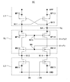
본원 발명자들은 고내압 구조의 트랜지스터를 사용하지 않고, 또한 트랜지스터의 게이트 산화막에 과대한 전압이 가해지지 않도록, 저진폭(0V∼VDD)의 논리 신호에 의해, 고진폭(0V∼VPP)의 신호를 출력하는 기술(이하, 비교예라 함)에 대하여 검토하였다. 도 1은 비교예에 따른 레벨 시프트 회로의 회로도이다.(0 V to VPP) signal by a low amplitude (0 V to VDD) logic signal so that an excessive voltage is not applied to the gate oxide film of the transistor without using a high breakdown voltage structure transistor (Hereinafter referred to as a comparative example). 1 is a circuit diagram of a level shift circuit according to a comparative example.
비교예에 따른 레벨 시프트 회로 LSR은 인버터 INV, INV2와 게이트 제어 회로 GC와 중간 전위 생성 회로 IVG와 직렬 회로 SC를 구비한다. 게이트 제어 회로인 인버터 INV는, 저전원 전위(VDD)와 접지 전위(GND) 사이에, 게이트가 입력 신호(IN)에 접속되는 P채널형 MOS 트랜지스터(이하, 「PMOS 트랜지스터」라 함) QP1과, 게이트가 입력 신호(IN)에 접속되는 N채널형 MOS 트랜지스터(이하, 「NMOS 트랜지스터」라 말함) QN1이 직렬로 접속되어 구성되어 있다. IN은 0∼VDD의 저진폭 신호이다. 게이트 제어 회로인 인버터 INV2는, 저전원 전위(VDD)와 접지 전위(GND) 사이에, 게이트가 반전 신호(/IN)에 접속되는 PMOS 트랜지스터 QP2와, 게이트가 반전 신호(/IN)에 접속되는 NMOS 트랜지스터 QN2가 직렬로 접속되어 구성되어 있다. 인버터 INV2는 제1 신호(IN2)를 생성한다.The level shift circuit LSR according to the comparative example includes inverters INV and INV2, a gate control circuit GC, an intermediate potential generation circuit IVG, and a serial circuit SC. The inverter INV which is a gate control circuit is provided between a low power supply potential VDD and a ground potential GND and includes a P-channel type MOS transistor QP1 (hereinafter referred to as a "PMOS transistor") whose gate is connected to the input signal IN And an N-channel MOS transistor QN1 (hereinafter referred to as " NMOS transistor ") whose gate is connected to the input signal IN. IN is a low amplitude signal of 0 to VDD. The inverter INV2 which is a gate control circuit includes a PMOS transistor QP2 having a gate connected to the inverted signal / IN and a gate connected to the inverted signal / IN between the low power supply potential VDD and the ground potential GND And an NMOS transistor QN2 are connected in series. The inverter INV2 generates the first signal IN2.
게이트 제어 회로 GC는 제2 신호(Vg)를 생성한다. 상세는 후술한다. 중간 전위 생성 회로 IVG는 제1 전위(Vrefp1), 제2 전위(Vrefp2) 및 제3 전위(Vrefn)를 생성한다. 상세는 후술한다.The gate control circuit GC generates the second signal Vg. Details will be described later. The intermediate potential generation circuit IVG generates the first potential Vrefp1, the second potential Vrefp2, and the third potential Vrefn. Details will be described later.
직렬 회로 SC는, 고전원 전위(VPP)와 접지 전위(GND) 사이에, PMOS 트랜지스터 MP1과, PMOS 트랜지스터 MP2와, NMOS 트랜지스터 MN2와, NMOS 트랜지스터 MN1이 직렬 접속되어 구성되어 있다. PMOS 트랜지스터 MP1의 게이트에 제2 신호(Vg)가 인가된다. PMOS 트랜지스터 MP2의 게이트에 제1 전위(Vrefp1)가 인가된다. NMOS 트랜지스터 MN2의 게이트에 제2 전위(Vrefn)가 인가된다. NMOS 트랜지스터 MN1의 게이트에 인버터 INV2의 출력 신호인 제1 신호(IN2)가 인가된다. 제2 신호(Vg)는 VPP/2∼VPP의 전위의 신호이다. 제1 전위(Vrefp1) 및 제3 전위(Vrefn)는 VPP/2 근방의 전위이다. PMOS 트랜지스터 MP1의 기판 전극이 고전원 전위(VPP)에 접속되고, NMOS 트랜지스터 MN1의 기판 전극이 접지 전위(GND)에 접속된다. PMOS 트랜지스터 MP2의 기판 전극이 PMOS 트랜지스터 MP2의 소스에 접속되고, NMOS 트랜지스터 MN2의 기판 전극이 NMOS 트랜지스터 MN2의 소스에 접속되고, PMOS 트랜지스터 MP2와 NMOS 트랜지스터 MN2의 접속점으로부터 출력 신호(OUT)가 취출되고 있다.In the serial circuit SC, a PMOS transistor MP1, a PMOS transistor MP2, an NMOS transistor MN2, and an NMOS transistor MN1 are connected in series between a high power supply potential VPP and a ground potential GND. And the second signal (Vg) is applied to the gate of the PMOS transistor MP1. And the first potential Vrefp1 is applied to the gate of the PMOS transistor MP2. And the second potential Vrefn is applied to the gate of the NMOS transistor MN2. The first signal IN2, which is the output signal of the inverter INV2, is applied to the gate of the NMOS transistor MN1. The second signal Vg is a signal of the potential of VPP / 2 to VPP. The first potential Vrefp1 and the third potential Vrefn are potentials near VPP / 2. The substrate electrode of the PMOS transistor MP1 is connected to the high power supply potential VPP and the substrate electrode of the NMOS transistor MN1 is connected to the ground potential GND. The substrate electrode of the PMOS transistor MP2 is connected to the source of the PMOS transistor MP2, the substrate electrode of the NMOS transistor MN2 is connected to the source of the NMOS transistor MN2, the output signal OUT is taken out from the connection point of the PMOS transistor MP2 and the NMOS transistor MN2 have.
저전원 전위(VDD)와 접지 전위(GND) 사이에 접속되는 트랜지스터와, 고전원 전위(VPP)와 접지 전위(GND) 사이에 접속되는 트랜지스터는 동일한 프로세스로 형성되는 저내압 디바이스이다. 바꾸어 말하면, 인버터 INV를 구성하는 트랜지스터와 직렬 회로 SC를 구성하는 트랜지스터의 내압은 동일 정도이고, 각 트랜지스터의 내압은 VDD보다도 높지만, VPP보다도 낮다. VDD는 예를 들어 1.8V, VPP는 예를 들어 3.3V, GND는 예를 들어 0V이다.A transistor connected between the low power supply potential VDD and the ground potential GND and a transistor connected between the high power supply potential VPP and the ground potential GND are low voltage resistant devices formed by the same process. In other words, the transistors constituting the inverter INV and the transistors constituting the serial circuit SC have the same level of breakdown voltage, and the breakdown voltage of each transistor is higher than VDD but lower than VPP. VDD is, for example, 1.8V, VPP is, for example, 3.3V, and GND is, for example, 0V.
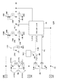
도 2는 게이트 제어 회로의 회로도이다. 게이트 제어 회로 GC는 고전원 전위(VPP)와 접지 전위(GND)간에, PMOS 트랜지스터 MP11과, 게이트에 제2 전위(Vrefp2)가 인가된 PMOS 트랜지스터 MP12와, 게이트에 제3 전위(Vrefn)가 인가된 NMOS 트랜지스터 MN12와, 게이트에 입력 신호(IN)가 인가된 NMOS 트랜지스터 MN11이 직렬 접속된 직렬 회로가 설치되어 있다.2 is a circuit diagram of the gate control circuit. The gate control circuit GC includes a PMOS transistor MP11, a PMOS transistor MP12 to which a second potential Vrefp2 is applied to the gate, and a PMOS transistor MP12 to which a third potential Vrefn is applied to the gate, between the high potential VPP and the ground potential GND And an NMOS transistor MN11 to which a gate is applied with an input signal IN are connected in series.
또한, 게이트 제어 회로 GC는 고전원 전위(VPP)와 접지 전위(GND)간에, PMOS 트랜지스터 MP13과, 게이트에 제2 전위(Vrefp2)가 인가된 PMOS 트랜지스터 MP14와, 게이트에 제3 전위(Vrefn)가 인가된 NMOS 트랜지스터 MN14와, 게이트에 반전 신호(/IN)가 인가된 NMOS 트랜지스터 MN13이 직렬 접속된 직렬 회로가 설치되어 있다.The gate control circuit GC includes a PMOS transistor MP13, a PMOS transistor MP14 to which a second potential Vrefp2 is applied to the gate, and a third potential Vrefn to the gate, between the high potential VPP and the ground potential GND. And an NMOS transistor MN13 to which a gate is applied with an inverted signal (/ IN) are connected in series.
PMOS 트랜지스터 MP11의 게이트가 PMOS 트랜지스터 MP13과 MP14의 접속점인 노드 N13에, PMOS 트랜지스터 MP13의 게이트가 PMOS 트랜지스터 MP11과 PMOS 트랜지스터 MP12의 접속점인 노드 N11에 접속된다. 그와 함께, PMOS 트랜지스터 MP11, MP13의 기판 전극이 VPP에, NMOS 트랜지스터 MN11, MN13의 기판 전극이 GND에 접속된다. PMOS 트랜지스터 MP12, MP14의 기판 전극이 각각 PMOS 트랜지스터 MP12, MP14의 소스에 접속되고, NMOS 트랜지스터 MN12, MN14의 기판 전극이 각각 NMOS 트랜지스터 MN12, MN14의 소스에 접속된다. 노드 N13과 접속되는 노드 N4로부터 게이트 전위(Vg)가 취출되고 있다. Vrefp2=VPP/2-|Vtp|로 함으로써, Vg는 VPP/2∼VPP 사이의 진폭의 전위로 된다.The gate of the PMOS transistor MP11 is connected to the node N13 where the PMOS transistors MP13 and MP14 are connected to each other and the gate of the PMOS transistor MP13 is connected to the node N11 which is the connection point between the PMOS transistor MP11 and the PMOS transistor MP12. At the same time, the substrate electrodes of the PMOS transistors MP11 and MP13 are connected to VPP and the substrate electrodes of the NMOS transistors MN11 and MN13 are connected to GND. Substrate electrodes of the PMOS transistors MP12 and MP14 are respectively connected to the sources of the PMOS transistors MP12 and MP14, and substrate electrodes of the NMOS transistors MN12 and MN14 are connected to the sources of the NMOS transistors MN12 and MN14, respectively. And the gate potential Vg is taken out from the node N4 connected to the node N13. Vrefp2 = VPP / 2 - | Vtp |, Vg becomes the potential of the amplitude between VPP / 2 and VPP.
PMOS 트랜지스터 MP11과 PMOS 트랜지스터 MP13은 서로 게이트와 드레인을 크로스 커플함으로써 래치 회로 LT가 구성되어, 정상 전류를 차단할 수 있다.The PMOS transistor MP11 and the PMOS transistor MP13 cross each other between the gate and the drain to constitute the latch circuit LT and can interrupt the normal current.
PMOS 트랜지스터 MP12, MP14와 NMOS 트랜지스터 MN12, MN14로 클램프 회로 CL이 구성된다. PMOS 트랜지스터 MP11, MP13의 드레인 전위는 클램프 회로 CL에 의해 Vrefp2까지만 강하한다. NMOS 트랜지스터 MN11, MN13의 드레인 전위는 클램프 회로 CL에 의해 Vrefn까지만 상승한다.The clamp circuit CL is composed of the PMOS transistors MP12 and MP14 and the NMOS transistors MN12 and MN14. The drain potentials of the PMOS transistors MP11 and MP13 drop only to Vrefp2 by the clamp circuit CL. The drain potential of the NMOS transistors MN11 and MN13 rises to Vrefn only by the clamp circuit CL.
NMOS 트랜지스터 MN11, MN13으로 래치 반전 회로 LI가 구성되고, 입력 신호(IN) 및 반전 신호(/IN)에 기초하여 래치 회로 LT의 상태를 반전할 수 있다.The NMOS transistors MN11 and MN13 constitute a latch inversion circuit LI and can invert the state of the latch circuit LT based on the input signal IN and the inversion signal / IN.
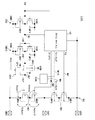
도 3은 중간 전위 생성 회로의 회로도이다. 중간 전위 생성 회로 IVG는 고전원 전위(VPP)와 접지 전위(GND) 사이에 저항 소자 R1 및 저항 소자 R2가 직렬 접속되고, 제1 전위(Vrefp1) 및 제3 전위(Vrefn)는 저항 소자 R1과 저항 소자 R2의 접속점으로부터 취출되고 있고, 저항 소자 R1의 저항값을 r1, 저항 소자 R2의 저항값을 r2라 하면,3 is a circuit diagram of the intermediate potential generation circuit. The intermediate potential generation circuit IVG has the resistance element R1 and the resistance element R2 connected in series between the high potential VPP and the ground potential GND and the first potential Vrefp1 and the third potential Vrefn are connected to the resistance element R1 When the resistance value of the resistance element R1 is r1 and the resistance value of the resistance element R2 is r2,
그 값은 다음 식(1)에 의해 주어진다.The value is given by the following equation (1).
![]()
![]()
본 예에서는 Vrefp1=Vrefn이지만, VPP/2 근방의 전압이면 Vrefp1≠Vrefn이어도 된다. 중간 전위 생성 회로 IVG는 고전원 전위(VPP)와 접지 전위(GND) 사이에 저항 소자 R3 및 저항 소자 R4가 직렬 접속되고, 제2 전위(Vrefp2)는 저항 소자 R3과 저항 소자 R4의 접속점으로부터 취출되고 있고, 저항 소자 R3의 저항값을 r3, 저항 소자 R4의 저항값을 r4로 하면, 그 값은 다음 식(2)에 의해 주어진다.Although Vrefp1 = Vrefn in this example, Vrefp1 may be equal to Vrefn if it is a voltage in the vicinity of VPP / 2. The intermediate potential generating circuit IVG has the resistor element R3 and the resistor element R4 connected in series between the high power supply potential VPP and the ground potential GND and the second potential Vrefp2 is taken out from the connection point of the resistor element R3 and the resistor element R4 And the resistance value of the resistance element R3 is r3 and the resistance value of the resistance element R4 is r4, the value is given by the following equation (2).
![]()
![]()
저항 소자 R1, R2, R3, R4는 PMOS 트랜지스터나 NMOS 트랜지스터로 형성해도 된다.The resistance elements R1, R2, R3, and R4 may be PMOS transistors or NMOS transistors.
다음에 동작의 설명을 한다. 여기서, "H"는 저전원 전위(VDD), "HH"는 고전원 전위(VPP), "L"은 접지 전위(GND)이다. 접지 전위는 기준 전위라고도 한다.Next, the operation will be described. Here, "H" is the low power supply potential VDD, "HH" is the high power supply potential VPP, and "L" is the ground potential GND. The ground potential is also referred to as a reference potential.
먼저, 입력 신호(IN)가 "L"인 경우, 노드 N1은 "H"로 되고, NMOS 트랜지스터 MN1이 오프함과 함께, 게이트 제어 회로 GC의 출력의 노드 N4가 Vrefp2+|Vtp|이므로 (VPP-Vrefp2-|Vtp|)>|Vtp|이면, PMOS 트랜지스터 MP1이 온하여 PMOS 트랜지스터 MP1과 PMOS 트랜지스터 MP2의 접속점인 노드 N3이 "HH"로 풀업된다. (VPP-Vrefp1)>|Vtp|이면, PMOS 트랜지스터 MP2도 온하여 출력 신호(OUT)도 "HH"로 되고, 또한 NMOS 트랜지스터 MN1과 NMOS 트랜지스터 MN2의 접속점인 노드 N2가 (Vrefn-Vtn)까지, NMOS 트랜지스터 MN2를 통해, 풀업되어 안정된다.First, when the input signal IN is "L ", the node N1 becomes" H ", and the NMOS transistor MN1 turns off and the node N4 of the output of the gate control circuit GC becomes Vrefp2 + | Vtp | Vrefp2- | Vtp |)> | Vtp |, the PMOS transistor MP1 is turned on and the node N3, which is the connection point between the PMOS transistor MP1 and the PMOS transistor MP2, is pulled up to "HH". The output signal OUT also becomes "HH ", and the node N2, which is the connection point of the NMOS transistor MN1 and the NMOS transistor MN2, reaches (Vrefn-Vtn) Is pulled up and stabilized through the NMOS transistor MN2.
한편, 입력 신호(IN)가 "H"인 경우, 노드 N1은 "L"로 되고, NMOS 트랜지스터 MN1이 온하여 NMOS 트랜지스터 MN1과 NMOS 트랜지스터 MN2의 접속점인 노드 N2가 "L"로 풀다운된다. Vrefn>Vtn이면 NMOS 트랜지스터 MN2도 온하여 출력 신호(OUT)도 "L"로 된다. 또한 출력의 노드 N4가 "HH"이므로, PMOS 트랜지스터 MP1이 오프하고, 따라서, 노드 N3이 (Vrefp1+|Vtp|)까지, PMOS 트랜지스터 MP2를 통해 풀다운 되어 안정된다.On the other hand, when the input signal IN is "H ", the node N1 becomes" L ", and the NMOS transistor MN1 is turned on and the node N2 which is the connection point of the NMOS transistor MN1 and the NMOS transistor MN2 is pulled down to "L ". When Vrefn > Vtn, the NMOS transistor MN2 also turns on and the output signal OUT also becomes "L ". Since the node N4 of the output is "HH ", the PMOS transistor MP1 is turned off, and thus the node N3 is pulled down through the PMOS transistor MP2 and stabilized to (Vrefp1 + | Vtp |).
이상 설명한 바와 같이, 도 1에 도시한 비교예에 따르면, VDD∼GND간에서 진폭하는 입력 신호(IN)로 고전압을 제어하여, "L"과 "HH"의 출력 신호(OUT)를 얻을 수 있다. PMOS 트랜지스터 MP1의 드레인∼소스간에는 최고 (VPP-Vrefp2-|Vtp|)의 전압이, PMOS 트랜지스터 MP2의 드레인∼소스간에는 최고 (Vrefp1+|Vtp|)의 전압이, NMOS 트랜지스터 MN1의 드레인∼소스간에는 최고 (Vrefn-Vtn)의 전압이, NMOS 트랜지스터 MN2의 드레인∼소스간에는 최고 (VPP-Vrefn+Vtn)의 전압이 각각 인가된다. Vrefp1 및 Vrefn을 VPP/2 근방의 전압으로 설정함으로써, MOS 트랜지스터의 드레인∼소스간에 고전압(VPP)이 인가되는 것이 회피된다.As described above, according to the comparative example shown in Fig. 1, the high voltage is controlled by the input signal IN which is amplified between VDD and GND to obtain the output signal OUT of "L" and "HH" . (Vrefp1 + | Vtp |) between the drain and the source of the PMOS transistor MP2 and the highest voltage (Vrefp1 + | Vtp |) between the drain and the source of the PMOS transistor MP1 and the highest (Vrefn-Vtn) is applied between the drain and the source of the NMOS transistor MN2, and a voltage of the highest voltage VPP-Vrefn + Vtn is applied between the drain and the source of the NMOS transistor MN2. By setting Vrefp1 and Vrefn to voltages near VPP / 2, application of the high voltage VPP between the drain and the source of the MOS transistor is avoided.
또한, PMOS 트랜지스터 MP1의 게이트 산화막에는 최고 (VPP-Vrefp2-|Vtp|)의 전압이, PMOS 트랜지스터 MP2의 게이트 산화막에는 최고 (VPP-Vrefp1)의 전압이, NMOS 트랜지스터 MN1의 게이트 산화막에는 최고 VDD의 전압이, NMOS 트랜지스터 MN2의 게이트 산화막에는 최고 Vrefn의 전압이 각각 인가된다. Vrefp1 및 Vrefn을 VPP/2 근방의 전압으로 설정함으로써 MOS 트랜지스터의 게이트 산화막에 강전계가 인가되는 것이 회피된다.(VPP-Vrefp2- | Vtp |) is applied to the gate oxide film of the PMOS transistor MP1, a voltage of the highest (VPP-Vrefp1) is applied to the gate oxide film of the PMOS transistor MP2, And a voltage of Vrefn is applied to the gate oxide film of the NMOS transistor MN2, respectively. By setting Vrefp1 and Vrefn to voltages near VPP / 2, it is avoided that a strong field is applied to the gate oxide film of the MOS transistor.
이들에 의해, PMOS 트랜지스터 MP1, MP2 및 NMOS 트랜지스터 MN1, MN2를 고내압 구조로 할 필요가 없어지기 때문에, 제조 공정이 복잡화되어 제조 비용이 높아진다고 하는 문제점도 해소된다.This eliminates the need for the PMOS transistors MP1 and MP2 and the NMOS transistors MN1 and MN2 to have a high breakdown voltage structure, thereby solving the problem that the manufacturing process is complicated and the manufacturing cost is increased.
그러나, 출력 신호(OUT)가 "HH"로부터 "L"로 천이하는 경우, 인버터 IV2의 출력 신호(IN2)는 "H"에서 Vgsn1=VDD로 된다. 노드 N2의 전위는 Vdsn1로 된다. Vgsn2는 Vrefn-Vdsn1이며, Vrefn=VPP/2로 하면, Vgsn2=VPP/2-Vdsn1로 된다. 실제의 사용예로서, VPP=3.3V, VDD=1.8V로 가정하면, Vgsn2=1.65V-Vdsn1, Vgsn1=1.8V이며, Vgsn2<Vgsn1로 된다. 이에 의해, NMOS 트랜지스터 MN2의 온 저항이 NMOS 트랜지스터 MN1의 온 저항보다도 커져, Vdsn2>Vdsn1로 되기 때문에, NMOS 트랜지스터 MN2의 소스-드레인간 전압이 커진다. Vdsn2=VPP-Vdsn1=3.3V-Vdsn1=1.8V+1.5V-Vdsn1=VDD+1.5V-Vdsn1이며, Vdsn1<1.5V로 되면, Vdsn2>VDD로 된다.However, when the output signal OUT transits from "HH" to "L ", the output signal IN2 of the inverter IV2 changes from" H "to Vgsn1 = VDD. The potential of the node N2 becomes Vdsn1. Vgsn2 is Vrefn-Vdsn1, and when Vrefn = VPP / 2, Vgsn2 = VPP / 2-Vdsn1. Assuming that VPP = 3.3V and VDD = 1.8V as practical examples, Vgsn2 = 1.65V-Vdsn1 and Vgsn1 = 1.8V, and Vgsn2 < Vgsn1. As a result, the on-resistance of the NMOS transistor MN2 becomes larger than the on-resistance of the NMOS transistor MN1, and Vdsn2 > Vdsn1, so that the source-drain voltage of the NMOS transistor MN2 becomes larger. Vdsn2 = VPP-Vdsn1 = 3.3V-Vdsn1 = 1.8V + 1.5V-Vdsn1 = VDD + 1.5V-Vdsn1. When Vdsn1 < 1.5V, Vdsn2 >
또한, 출력 신호(OUT)가 "L"로부터 "HH"로 천이하는 경우, 노드 N4는 Vrefp2+|Vtp|에서 Vgsp1=VPP-Vrefp2-|Vtp|로 된다. Vrefp2=VPP/2-|Vtp|로 하면, Vgsp1=VPP/2로 된다. 노드 N3의 전위는 VPP-Vdsp1로 된다. Vgsp2는 (VPP-Vdsp1)-Vrefp1이며, Vrefp1=VPP/2로 하면, Vgsp2=VPP/2-Vdsp1로 된다. 실제의 사용예로서, VPP=3.3V, VDD=1.8V로 가정하면, Vgsp2=1.65V-Vdsp1, Vgsp1=1.65V이며, Vdsp1>0V이므로 Vgsp2<Vgsp1로 된다. 이에 의해, PMOS 트랜지스터 MP2의 온 저항이 PMOS 트랜지스터 MP1의 온 저항보다도 커져, Vdsp2>Vdsp1로 되기 때문에, PMOS 트랜지스터 MP2의 소스-드레인간 전압이 커진다. Vdsp2=VPP-Vdsp1=3.3V-Vdsp1=1.8V+1.5V-Vdsp1=VDD+1.5V-Vdsp1이며, Vdsp1<1.5V로 되면, Vds2>VDD로 된다.Further, when the output signal OUT transits from "L" to "HH ", the node N4 becomes Vgsp1 = VPP-Vrefp2- | Vtp | at Vrefp2 + | Vtp |. Vrefp2 = VPP / 2 - | Vtp |, Vgsp1 = VPP / 2. The potential of the node N3 becomes VPP-Vdsp1. Vgsp2 is (VPP-Vdsp1) -Vrefp1, and when Vrefp1 = VPP / 2, Vgsp2 = VPP / 2-Vdsp1. Assuming that VPP = 3.3V and VDD = 1.8V, Vgsp2 = 1.65V-Vdsp1 and Vgsp1 = 1.65V and Vdsp1 > 0V, Vgsp2 < Thereby, the ON resistance of the PMOS transistor MP2 becomes larger than the ON resistance of the PMOS transistor MP1, and Vdsp2 > Vdsp1 becomes high, so that the source-drain voltage of the PMOS transistor MP2 becomes large. Vdsp2 = VPP-Vdsp1 = 3.3V-Vdsp1 = 1.8V + 1.5V-Vdsp1 = VDD + 1.5V-Vdsp1, and Vdsp1 <
핫 캐리어(HCI) 열화와 Vds의 관계는, 일반적으로, 하기의 식(3)으로 나타내어진다.The relationship between hot carrier (HCI) deterioration and Vds is generally expressed by the following equation (3).
![]()
![]()
즉, Vds2가 크면 NMOS 트랜지스터 MN2의 핫 캐리어 열화가 지수 함수적으로 증가하게 된다. 특히 상기 회로에서는, 저내압 트랜지스터를 사용하여, 고진폭의 신호를 출력하고 있기 때문에, 상기와 같이 VDD를 초과하는 Vds가 인가되는 경우가 있어, 열화가 심해진다.That is, if Vds2 is large, the hot carrier deterioration of the NMOS transistor MN2 exponentially increases. Particularly, in the above circuit, since a low-voltage transistor is used to output a signal of a high amplitude, Vds exceeding VDD may be applied as described above, and the deterioration becomes serious.
<실시 형태><Embodiment>
Vgsn1을 낮게 하는 수단(인버터 INV의 출력 전위를 낮게 하는 전위 변환 회로)을 게이트 제어 회로인 인버터 INV와 N채널형 MOS 트랜지스터 MN1의 게이트 사이에 설치한다. 또한, Vgsp1을 낮게 하는 수단(게이트 제어 회로 GC의 출력 전위를 높게 하는 전위 변환 회로)을 게이트 제어 회로 GC와 P채널형 MOS 트랜지스터 MP1의 게이트 사이에 설치한다.A means for lowering Vgsn1 (a potential conversion circuit for lowering the output potential of the inverter INV) is provided between the inverter INV as the gate control circuit and the gate of the N-channel type MOS transistor MN1. A means for lowering Vgsp1 (a potential conversion circuit for raising the output potential of the gate control circuit GC) is provided between the gate of the gate control circuit GC and the gate of the P-channel type MOS transistor MP1.
이에 의해, Vgsn1≒Vgsn2, Vgsp1≒Vgsp2로 되면, Vdsn1≒Vdsn2≒VPP/2=1.65V<1.8V=VDD, Vdsp1≒Vdsp2≒VPP/2=1.65V<1.8V=VDD로 되어, Vdsn2, Vdsp2를 낮게 할 수 있다.Thus, when Vgsn1? Vgsn2 and Vgsp1? Vgsp2 are satisfied, Vdsn1? Vdsn2? VPP / 2 = 1.65V 1.8V = VDD, Vdsp1? Vdsp2? VPP / 2 = 1.65V <1.8V = VDD, Can be lowered.
[실시예 1][Example 1]
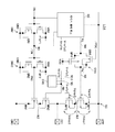
도 4는 실시예 1에 따른 레벨 시프트 회로의 회로도이다. 레벨 시프트 회로 LS1은 인버터 INV2의 출력과 NMOS 트랜지스터 MN1의 게이트 사이에 전위 변환 회로 CV1을 추가하고 있는 점을 제외하고, 레벨 시프트 회로 LSR과 마찬가지이다. 전위 변환 회로 CV1은 NMOS 트랜지스터 QN3(NMOS 트랜스퍼 게이트)을 포함하고, NMOS 트랜지스터 QN3은 출력 전위를 입력 전위와 상이하게 한다. NMOS 트랜지스터 QN3의 게이트에 VDD가 인가되고, NMOS 트랜지스터 QN3의 기판 전극은 NMOS 트랜지스터 MN1의 게이트(노드 N7)가 접속된다. 인버터 INV2의 출력 진폭은 0∼VDD이며, NMOS 트랜지스터 QN3을 통한 노드 N7의 과도 상태의 진폭은 0∼(VDD-Vtn)으로 된다. Vtn은 NMOS 트랜지스터 QN3의 역치이다. 그것에 의해 NMOS 트랜지스터 MN1의 온 시의 Vgsn1은 VDD-Vtn으로 되고, 비교예와 비교하여 Vtn분 작아진다. Vgsn1이 작아짐으로써, NMOS 트랜지스터 MN1의 온 저항은 높아져, Vdsn1이 커진다. 노드 N2의 전위는 NMOS 트랜지스터 MN1과 NMOS 트랜지스터 MN2의 분압에 의해 정해지기 때문에, Vdsn1이 커지면 Vdsn2는 작아진다. 전술한 식(3)의 관계로부터, Vdsn2가 작아짐으로써, NMOS 트랜지스터 MN2의 핫 캐리어 열화를 억제할 수 있다. 직렬 회로 SC에서는, PMOS 트랜지스터 MP2의 기판 전극이 PMOS 트랜지스터 MP2의 소스에 접속되고, NMOS 트랜지스터 MN2의 기판 전극이 NMOS 트랜지스터 MN2의 소스에 접속되어 있지만, PMOS 트랜지스터 MP2의 기판 전극이 고전원 전위(VPP)에 접속되고, NMOS 트랜지스터 MN2의 기판 전극이 접지 전위(GND)에 접속되는 구성이어도 된다. 직렬 회로의 구성의 변경은 이하의 실시예 2∼5에도 적용할 수 있다. 또한, 게이트 제어 회로 GC에서는, PMOS 트랜지스터 MP12, MP14의 기판 전극이 각각 PMOS 트랜지스터 MP12, MP14의 소스에 접속되고, NMOS 트랜지스터 MN12, MN14의 기판 전극이 각각 NMOS 트랜지스터 MN12, MN14의 소스에 접속되어 있지만, PMOS 트랜지스터 MP12, MP14의 기판 전극이 각각 VPP에 접속되고, NMOS 트랜지스터 MN12, MN14의 기판 전극이 각각 GND에 접속되는 구성이어도 된다. 게이트 제어 회로의 구성의 변경은 이하의 실시예 2∼5에도 적용할 수 있다.4 is a circuit diagram of the level shift circuit according to the first embodiment. The level shift circuit LS1 is the same as the level shift circuit LSR except that the potential conversion circuit CV1 is added between the output of the inverter INV2 and the gate of the NMOS transistor MN1. The potential conversion circuit CV1 includes an NMOS transistor QN3 (NMOS transfer gate), and the NMOS transistor QN3 makes the output potential different from the input potential. VDD is applied to the gate of the NMOS transistor QN3, and the gate (node N7) of the NMOS transistor MN1 is connected to the substrate electrode of the NMOS transistor QN3. The output amplitude of the inverter INV2 is 0 to VDD, and the amplitude of the transient state of the node N7 through the NMOS transistor QN3 is 0 to (VDD-Vtn). Vtn is a threshold value of the NMOS transistor QN3. Thereby, Vgsn1 at the time of turning on of the NMOS transistor MN1 becomes VDD-Vtn, which is smaller than Vtn in comparison with the comparative example. As Vgsn1 becomes smaller, the on-resistance of the NMOS transistor MN1 becomes higher and Vdsn1 becomes larger. Since the potential of the node N2 is determined by the partial pressures of the NMOS transistor MN1 and the NMOS transistor MN2, Vdsn2 becomes smaller when Vdsn1 becomes larger. From the relationship of the above-described equation (3), it is possible to suppress hot carrier deterioration of the NMOS transistor MN2 by reducing Vdsn2. In the serial circuit SC, the substrate electrode of the PMOS transistor MP2 is connected to the source of the PMOS transistor MP2 and the substrate electrode of the NMOS transistor MN2 is connected to the source of the NMOS transistor MN2. However, the substrate electrode of the PMOS transistor MP2 is connected to the high- And the substrate electrode of the NMOS transistor MN2 is connected to the ground potential GND. Modification of the configuration of the series circuit is also applicable to the following Embodiments 2 to 5. In the gate control circuit GC, the substrate electrodes of the PMOS transistors MP12 and MP14 are respectively connected to the sources of the PMOS transistors MP12 and MP14, and the substrate electrodes of the NMOS transistors MN12 and MN14 are respectively connected to the sources of the NMOS transistors MN12 and MN14 , And the substrate electrodes of the PMOS transistors MP12 and MP14 are respectively connected to the VPP and the substrate electrodes of the NMOS transistors MN12 and MN14 are connected to the GND, respectively. The modification of the configuration of the gate control circuit is also applicable to the following Embodiments 2 to 5.
도 5는 실시예 1에 따른 반도체 장치의 블록도이다. 반도체 장치(50)는 반도체 장치인 SoC(51)와 전원 IC(52)를 구비한다. SoC(51)는 내부 회로(53)와 I/O 회로(54, 55)를 하나의 반도체 기판(반도체 칩) 상에 구비한다. 레벨 시프트 회로 LS1은 I/O 회로(54, 55)의 출력 회로에 사용된다. 또한, 본 예에서는, I/O 회로(54)는 출력 회로, I/O 회로(55)는 입력 회로 및 출력 회로로서 동작한다. 전원 IC(52)로부터 고전원 전위(VPP=3.3V) 및 저전원 전위(VDD)가 SoC(51)의 I/O 회로(54, 55)에 공급된다. 내부 회로(53)로부터 출력되는 신호의 진폭은 0V∼VDD이며, I/O 회로(54, 55)에 공급된다. I/O 회로(54, 55)의 레벨 시프트 회로 LS1에 의해 진폭이 0V∼VDD인 신호의 진폭이 0V∼VPP인 신호로 변환되어, SoC(51)의 외부에 출력된다.5 is a block diagram of the semiconductor device according to the first embodiment. The
[실시예 2][Example 2]
도 6은 실시예 2에 따른 레벨 시프트 회로의 회로도이다. 실시예 2에 따른 레벨 시프트 회로 LS2는 고전원 전위(VPP)가 높을 때의 핫 캐리어 열화의 억제와, VPP가 낮을 때(MOS 트랜지스터의 내압을 초과하지 않는 정도)의 고속 동작을 양립하는 회로이다. 레벨 시프트 회로 LS2는 전위 변환 회로를 제외하고, 레벨 시프트 회로 LS1과 마찬가지이다. 전위 변환 회로 CV2는, NMOS 트랜지스터 QN3과 병렬로 접속되는 PMOS 트랜지스터 QP3(PMOS 트랜스퍼 게이트)을 구비한다. PMOS 트랜지스터 QP3의 게이트에 POC 신호가 인가되고, PMOS 트랜지스터 QP3의 기판 전극은 인버터 INV2의 출력이 접속된다. VPP가 높을 때는, POC 신호를 "H"(VDD)로 하고, PMOS 트랜지스터 QP3을 오프로 한다. 그 경우, 회로 동작은 실시예 1과 마찬가지이며, 노드 N7의 "H" 레벨이 (VDD-Vtn)으로 됨으로써, 실시예 1과 마찬가지로 NMOS 트랜지스터 QN2의 핫 캐리어 열화를 억제할 수 있다. VPP가 낮을 때는, POC 신호를 "L"(GND)로 하고, PMOS 트랜지스터 QP3을 온으로 한다. 이에 의해, 노드 N7의 "H" 레벨은 VDD로 되고, 진폭은 0V∼VDD로 되어, 고속 동작이 가능해진다.6 is a circuit diagram of the level shift circuit according to the second embodiment. The level shift circuit LS2 according to the second embodiment is a circuit that both suppresses deterioration of hot carriers when the high power supply potential VPP is high and high speed operation when VPP is low (does not exceed the breakdown voltage of the MOS transistor) . The level shift circuit LS2 is the same as the level shift circuit LS1 except for the potential conversion circuit. The potential conversion circuit CV2 includes a PMOS transistor QP3 (PMOS transfer gate) connected in parallel with the NMOS transistor QN3. The POC signal is applied to the gate of the PMOS transistor QP3 and the output of the inverter INV2 is connected to the substrate electrode of the PMOS transistor QP3. When the VPP is high, the POC signal is set to "H" (VDD) and the PMOS transistor QP3 is turned off. In this case, the circuit operation is the same as in
도 7은 실시예 2에 따른 정보 기기의 블록도이다. 정보 기기(70)는 반도체 장치인 SoC(71)와 전원 IC(72)와 SD 메모리 카드(76)를 구비한다. SoC(71)는 SD 호스트 컨트롤러(73)와 I/O 회로(74, 75)를 하나의 반도체 기판(반도체 칩) 상에 구비한다. SD 호스트 컨트롤러(73)는 도시하지 않은 CPU와 SD 메모리 카드(76)간의 데이터나 제어 신호를 교환하기 위한 것이고, 예를 들어 클럭 신호(CLK)나 커맨드(CMD)를 출력하여, 데이터(DAT)의 송수신을 행한다. 레벨 시프트 회로 LS2는 I/O 회로(74, 75)의 출력 회로에 사용된다. 또한, 본 예에서는, I/O 회로(74)는 출력 회로, I/O 회로(75)는 입력 회로 및 출력 회로로서 동작한다. 전원 IC(72)로부터 고전원 전위(VPP=3.3V 또는 1.8V)가 SoC(71)의 I/O 회로(74, 75)에 공급된다. 전원 IC(72)로부터 저전원 전위(VDD=1.8V)가 SD 호스트 컨트롤러(73) 및 I/O 회로(74, 75)에 공급된다. 전원 IC(72)는, POC 신호가 "L"일 때는 1.8V를 공급하고, POC 신호가 "H"일 때는 3.3V를 공급한다. SD 호스트 컨트롤러(73)로부터 출력되는 신호의 진폭은 0V∼VDD이며, I/O 회로(74, 75)에 공급된다. 또한, 전원 IC(72)는 SoC(71)에 내장해도 된다.7 is a block diagram of an information device according to a second embodiment. The
SoC(71)와 SD 메모리 카드(76)의 신호의 교환은, 3.3V 레벨과 1.8V 레벨의 2개의 모드가 있다. 저속 동작시 3.3V 레벨에서, 고속 동작시 1.8V 레벨에서 동작한다. 예를 들어 SD 메모리 카드 규격 3.0에서는, 전원 전압이 3.3V일 때에 최대 50㎒, 전원 전압이 1.8V일 때에 최대 208㎒에서 동작하여, 전원 전압이 1.8V일 때쪽이 보다 고속 동작이 요구된다. SoC(71)의 전원 전위(VPP)는 전원 IC(72)로부터 3.3V 또는 1.8V가 공급된다. SoC(71)측의 POC 신호에 의해, 전원 IC(72)의 출력 전원 전위의 3.3V/1.8V의 전환을 행한다. 또한 제어 신호 POC에 의해, I/O 회로(74, 75)의 동작 모드의 3.3V/1.8V의 전환을 행하고, 1.8V일 때에 I/O 회로(74, 75)가 고속 동작하도록 회로를 전환한다.There are two modes of exchanging signals between the
[실시예 3][Example 3]
도 8은 실시예 3에 따른 레벨 시프트 회로의 회로도이다. 실시예 3에 따른 레벨 시프트 회로 LS3은 PMOS 트랜지스터의 핫 캐리어를 억제하는 회로이다. 레벨 시프트 회로 LS3은 게이트 제어 회로 GC와 PMOS 트랜지스터 MP1 사이에 전위 변환 회로 CV3을 추가하고 있는 점을 제외하고, 레벨 시프트 회로 LSR과 마찬가지이다. 전위 변환 회로 CV3은 PMOS 트랜지스터 QP4(PMOS 트랜스퍼 게이트)를 포함하고, 출력 전위를 입력 전위와 상이하게 한다. PMOS 트랜지스터 QP4의 게이트에 VDD가 인가되고, PMOS 트랜지스터 QP4의 기판 전극은 PMOS 트랜지스터 PN1의 게이트(노드 N8)가 접속된다. 그것에 의해, 노드 N8의 레벨은 (VPP/2+Vtp)∼VPP로 된다. 그것에 의해 Vgsp1이 작아지고, Vdsp1이 커진다. Vdsp1이 커지면, Vdsp2는 작아져, PMOS 트랜지스터 MP2의 핫 캐리어 열화가 억제된다. 레벨 시프트 회로 LS3은 실시예 1과 마찬가지로 SoC(51)의 I/O 회로(54, 55)에 사용된다.8 is a circuit diagram of the level shift circuit according to the third embodiment. The level shift circuit LS3 according to the third embodiment is a circuit for suppressing the hot carrier of the PMOS transistor. The level shift circuit LS3 is the same as the level shift circuit LSR except that the potential conversion circuit CV3 is added between the gate control circuit GC and the PMOS transistor MP1. The potential conversion circuit CV3 includes a PMOS transistor QP4 (PMOS transfer gate), and makes the output potential different from the input potential. VDD is applied to the gate of the PMOS transistor QP4, and the gate (node N8) of the PMOS transistor PN1 is connected to the substrate electrode of the PMOS transistor QP4. Thereby, the level of the node N8 is (VPP / 2 + Vtp) - VPP. As a result, Vgsp1 becomes smaller and Vdsp1 becomes larger. When Vdsp1 becomes larger, Vdsp2 becomes smaller, and hot carrier deterioration of the PMOS transistor MP2 is suppressed. The level shift circuit LS3 is used in the I /
[실시예 4][Example 4]
도 9는 실시예 4에 따른 레벨 시프트 회로의 회로도이다. 실시예 4에 따른 레벨 시프트 회로 LS4는 고전원 전위(VPP)가 높을 때의 핫 캐리어 열화의 억제와, VPP가 낮을 때(MOS 트랜지스터의 내압을 초과하지 않는 정도)의 고속 동작을 양립하는 회로이다. 레벨 시프트 회로 LS4는 전위 변환 회로를 제외하고, 레벨 시프트 회로 LS3과 마찬가지이다. 전위 변환 회로 CV4는 PMOS 트랜지스터 QN4와 병렬로 접속되는 NMOS 트랜지스터 QN4(NMOS 트랜스퍼 게이트)를 구비한다. NMOS 트랜지스터 QN4의 게이트에 /POC 신호가 인가되고, NMOS 트랜지스터 QN4의 기판 전극은 게이트 제어 회로 GC의 출력(노드 N4)이 접속된다. VPP가 높을 때는, /POC 신호를 "L"(GND)로 하여, NMOS 트랜지스터 QN4를 오프로 한다. 그 경우, 회로 동작은 실시예 3과 마찬가지이며, 노드 N8의 "L" 레벨이 (VPP/2+Vtp)로 됨으로써, 실시예 3과 마찬가지로 PMOS 트랜지스터 MP2의 핫 캐리어 열화를 억제할 수 있다. VPP가 낮을 때는, /POC 신호를 "H"(VDD)로 하여, NMOS 트랜지스터 QN4를 온으로 한다. 이에 의해, 노드 N8의 "L" 레벨은 VPP/2로 되고, 진폭은 VPP/2∼VPP로 되어, 고속 동작이 가능해진다. 레벨 시프트 회로 LS4는 실시예 2와 마찬가지로 SoC(71)의 I/O 회로(74, 75)에 사용된다. 이 경우, I/O 회로(74, 75)에는 /POC 신호가 입력된다.9 is a circuit diagram of the level shift circuit according to the fourth embodiment. The level shift circuit LS4 according to the fourth embodiment is a circuit that both suppresses deterioration of hot carriers when the high power supply potential VPP is high and high speed operation when VPP is low (does not exceed the breakdown voltage of the MOS transistor) . The level shift circuit LS4 is the same as the level shift circuit LS3 except for the potential conversion circuit. The potential conversion circuit CV4 includes an NMOS transistor QN4 (NMOS transfer gate) connected in parallel with the PMOS transistor QN4. The / POC signal is applied to the gate of the NMOS transistor QN4 and the output (node N4) of the gate control circuit GC is connected to the substrate electrode of the NMOS transistor QN4. When the VPP is high, the / POC signal is set to "L" (GND), and the NMOS transistor QN4 is turned off. In this case, the circuit operation is the same as in the third embodiment, and the "L" level of the node N8 is set to (VPP / 2 + Vtp), so that the hot carrier deterioration of the PMOS transistor MP2 can be suppressed in the same manner as in the third embodiment. When VPP is low, the / POC signal is set to "H" (VDD), and the NMOS transistor QN4 is turned on. Thereby, the "L" level of the node N8 becomes VPP / 2 and the amplitude becomes VPP / 2 to VPP, and high-speed operation becomes possible. The level shift circuit LS4 is used in the I /
[실시예 5][Example 5]
도 10은 실시예 5에 따른 레벨 시프트 회로의 회로도이다. 실시예 5에 따른 레벨 시프트 회로 LS5는 고전원 전위(VPP)가 높을 때, PMOS 트랜지스터 MP2 및 NMOS 트랜지스터 MN2의 양쪽의 핫 캐리어 열화의 억제와, VPP가 낮을 때(MOS 트랜지스터의 내압을 초과하지 않는 정도)의 고속 동작을 양립하는 회로이다. 레벨 시프트 회로 LS5는 실시예 2와 실시예 4를 조합한 회로이며, 그 동작은 실시예 2 및 실시예 4와 마찬가지이다. 레벨 시프트 회로 LS5는 실시예 2와 마찬가지로 SoC(71)의 I/O 회로(74, 75)에 사용된다. 이 경우, I/O 회로(74, 75)에는 POC 신호 및 /POC 신호가 입력된다.10 is a circuit diagram of the level shift circuit according to the fifth embodiment. The level shift circuit LS5 according to the fifth embodiment is capable of suppressing hot carrier deterioration of both the PMOS transistor MP2 and the NMOS transistor MN2 when the high power supply potential VPP is high and when the voltage VPP is low Speed operation of the first embodiment. The level shift circuit LS5 is a circuit combining Embodiment 2 and Embodiment 4, and the operation thereof is the same as Embodiment 2 and Embodiment 4. [ The level shift circuit LS5 is used in the I /
실시예에서는, 고내압 구조의 트랜지스터를 사용하지 않고, 또한 트랜지스터의 게이트 산화막에 과대한 전압이 가해지지 않도록, 저진폭(0V∼VDD)의 논리 신호에 의해, 고진폭(0V∼VPP)의 신호를 출력하는 회로에서, 출력부는 PMOS 트랜지스터 및 NMOS 트랜지스터를 각각 복수단 직렬로 접속한 구성이다.(0V to VPP) signal by a low amplitude (0V to VDD) logic signal so that an excessive voltage is not applied to the gate oxide film of the transistor without using a high breakdown voltage structure transistor, In an output circuit, a PMOS transistor and an NMOS transistor are respectively connected in series in a plurality of stages.
실시예 1, 2, 5에서는, NMOS 트랜지스터의 게이트와 게이트 제어 회로 사이에, 트랜스퍼 게이트를 접속함으로써, 세로 적층한 각각의 NMOS 트랜지스터에 가해지는 Vds(소스-드레인간 전압)를 적절하게 제어하여, 고전원 전위(VPP)가 높을 때의 NMOS 트랜지스터의 핫 캐리어 열화를 억제함과 함께, 실시예 2, 5에서는, VPP가 낮을 때에 고속 동작을 실현한다.In
실시예 3, 4, 5에서는, PMOS 트랜지스터의 게이트와 게이트 제어 회로 사이에, 트랜스퍼 게이트를 접속함으로써, 세로 적층한 각각의 PMOS에 가해지는 Vds(소스-드레인간 전압)를 적절하게 제어하여, 고전원 전위(VPP)가 높을 때의 PMOS 트랜지스터의 핫 캐리어 열화를 억제함과 함께, 실시예 4, 5에서는, VPP가 낮을 때에 고속 동작을 실현한다.In Examples 3, 4, and 5, Vds (source-drain voltage) applied to each vertically stacked PMOS is appropriately controlled by connecting a transfer gate between the gate of the PMOS transistor and the gate control circuit, The deterioration of the hot carrier of the PMOS transistor when the source potential VPP is high is suppressed, and in the fourth and fifth embodiments, the high-speed operation is realized when the VPP is low.
실시예에 따르면, 저내압 디바이스를 사용한 고전압 출력 회로의 신뢰성을 향상시킬 수 있다. 특히 신뢰성 열화가 현저해지는, 미세화된 최첨단 프로세스에 유효하다. 프로세스가 미세화됨에 따라서, 핫 캐리어에 의한 트랜지스터 성능의 열화가 현저해지고 있다.According to the embodiment, the reliability of the high-voltage output circuit using the low-voltage device can be improved. This is particularly effective for a finer state-of-the-art process in which reliability deterioration becomes remarkable. As the process becomes finer, deterioration of transistor performance due to hot carriers becomes remarkable.
이상, 본 발명자에 의해 이루어진 발명을 실시 형태 및 실시예에 기초하여 구체적으로 설명하였지만, 본 발명은 상기 실시 형태 및 실시예에 한정되는 것은 아니고, 다양하게 변경 가능한 것은 물론이다.While the invention made by the present inventors has been specifically described based on the embodiments and the examples, the present invention is not limited to the above-described embodiments and examples, and it goes without saying that the invention can be variously modified.
실시예 1과 실시예 3을 조합하여, 전위 변환 회로 CV1과 전위 변환 회로 CV3의 양쪽을 사용하도록 해도 된다.Both of the potential conversion circuit CV1 and the potential conversion circuit CV3 may be used in combination with the first and third embodiments.
실시예 1∼5는 출력 드라이버의 예이지만, 마찬가지로 트랜지스터를 세로 적층으로 하여 게이트 바이어스를 제어하여, 고전압에 견디도록 하는 회로에 대하여, 동일한 방법이 적용 가능하다.The first to fifth embodiments are examples of the output driver, but the same method can be applied to a circuit in which transistors are stacked vertically and gate bias is controlled so as to withstand a high voltage.
50 : 반도체 장치
70 : 정보 기기
51, 71 : SoC
52, 72 : 전원 IC
54, 74 : I/O 회로
55, 74 : I/O 회로
LS1, LS2, LS3, LS4, LS5 : 레벨 시프트 회로
GC : 게이트 제어 회로
IVG : 중간 전위 생성 회로
INV, INV2 : 인버터
MN1, MN2 : NMOS 트랜지스터
MP1, MP2 : PMOS 트랜지스터
QN3, QN4 : NMOS 트랜지스터
QP3, QP4 : PMOS 트랜지스터50: Semiconductor device
70: Information equipment
51, 71: SoC
52, 72: Power supply IC
54, 74: I / O circuit
55, 74: I / O circuit
LS1, LS2, LS3, LS4, LS5: Level shift circuit
GC: gate control circuit
IVG: intermediate potential generation circuit
INV, INV2: Inverter
MN1, MN2: NMOS transistor
MP1, MP2: PMOS transistor
QN3, QN4: NMOS transistor
QP3, QP4: PMOS transistor
Claims (20)
상기 레벨 시프트 회로는,
직렬 접속 회로와,
전위 생성 회로와,
제1 전원에 접속되는 제1 게이트 제어 회로와,
상기 제1 전원의 전위보다도 높은 제2 전원에 접속되는 제2 게이트 제어 회로와,
상기 제1 게이트 제어 회로와 상기 직렬 접속 회로 사이에 배치되는 제1 전위 변환 회로를 구비하고,
상기 직렬 접속 회로는,
소스가 상기 제2 전원에 접속되는 제1 P채널형 MOS 트랜지스터와,
소스가 상기 제1 P채널형 MOS 트랜지스터의 드레인에 접속되는 제2 P채널형 MOS 트랜지스터와,
소스가 기준 전원에 접속되는 제1 N채널형 MOS 트랜지스터와,
소스가 상기 제1 N채널형 MOS 트랜지스터의 드레인에 접속되는 제2 N채널형 MOS 트랜지스터와,
상기 제2 P채널형 MOS 트랜지스터의 드레인과 상기 제2 N채널형 MOS 트랜지스터의 드레인이 접속되는 제1 출력 노드를 구비하고,
상기 전위 생성 회로는, 상기 제2 전원의 전위보다도 낮고 상기 기준 전원의 전위보다도 높은 상기 제2 P채널형 MOS 트랜지스터의 게이트에 인가하는 제1 전위와, 상기 제2 전원의 전위보다도 낮고 상기 기준 전원의 전위보다도 높은 상기 제2 N채널형 MOS 트랜지스터의 게이트에 인가하는 제2 전위와, 상기 제2 전원의 전위보다도 낮고 상기 기준 전원의 전위보다도 높은 제3 전위를 생성하고,
상기 제1 게이트 제어 회로는, 상기 기준 전원의 전위와 상기 제1 전원의 전위 사이의 진폭이며, 제1 N채널형 MOS 트랜지스터의 게이트를 제어하는 제1 신호를 생성하고,
상기 제2 게이트 제어 회로는, 상기 제1 전위와 상기 제2 전원의 전위 사이의 진폭이며, 상기 제1 P채널형 MOS 트랜지스터의 게이트를 제어하는 제2 신호를 생성하고,
상기 제1 전위 변환 회로는 상기 제1 N채널형 MOS 트랜지스터의 게이트에 상기 제1 신호의 고레벨보다도 낮고 기준 전원의 전위보다도 높은 제1 레벨의 전위를 공급하는 반도체 장치.A semiconductor device includes a semiconductor chip having a level shift circuit for outputting a signal of a high amplitude by a logic signal of low amplitude,
The level shift circuit comprising:
A series connection circuit,
A potential generation circuit,
A first gate control circuit connected to the first power supply,
A second gate control circuit connected to a second power supply higher than the potential of the first power supply,
And a first potential conversion circuit disposed between the first gate control circuit and the series connection circuit,
Wherein the series connection circuit comprises:
A first P-channel type MOS transistor whose source is connected to the second power source,
A second P-channel MOS transistor whose source is connected to the drain of the first P-channel MOS transistor,
A first N-channel MOS transistor whose source is connected to a reference power supply,
A second N-channel MOS transistor whose source is connected to the drain of the first N-channel MOS transistor,
And a first output node to which a drain of the second P-channel MOS transistor and a drain of the second N-channel MOS transistor are connected,
The potential generation circuit includes a first potential applied to a gate of the second P-channel type MOS transistor which is lower than a potential of the second power source and higher than a potential of the reference power source, and a second potential which is lower than a potential of the second power source, And a third potential higher than the potential of the second power source and higher than the potential of the reference power source, and generates a third potential higher than the potential of the second power source and higher than the potential of the reference power source,
The first gate control circuit generates a first signal for controlling the gate of the first N-channel type MOS transistor, the amplitude being the amplitude between the potential of the reference power supply and the potential of the first power supply,
The second gate control circuit generates a second signal for controlling the gate of the first P-channel type MOS transistor, the amplitude being the amplitude between the first potential and the potential of the second power supply,
The first potential conversion circuit supplies a gate of the first N-channel type MOS transistor with a first level potential lower than the high level of the first signal and higher than the potential of the reference power supply.
상기 제1 P채널형 MOS 트랜지스터의 기판은 상기 제2 전원에 접속되고,
상기 제2 P채널형 MOS 트랜지스터의 기판은 상기 제1 P채널형 MOS 트랜지스터의 드레인에 접속되고,
상기 제1 N채널형 MOS 트랜지스터의 기판은 상기 기준 전원에 접속되고,
상기 제2 N채널형 MOS 트랜지스터의 기판은 상기 제1 N채널형 MOS 트랜지스터의 드레인에 접속되는 반도체 장치.The method according to claim 1,
A substrate of the first P-channel type MOS transistor is connected to the second power source,
The substrate of the second P-channel MOS transistor is connected to the drain of the first P-channel MOS transistor,
A substrate of the first N-channel type MOS transistor is connected to the reference power supply,
And the substrate of the second N-channel MOS transistor is connected to the drain of the first N-channel MOS transistor.
상기 제1 전위 변환 회로는 상기 제1 N채널형 MOS 트랜지스터의 게이트에 제1 제어 신호에 기초하여 상기 제1 레벨의 전위보다도 높은 전위를 공급하는 반도체 장치.The method according to claim 1,
And the first potential conversion circuit supplies a potential higher than the potential of the first level to the gate of the first N-channel type MOS transistor based on a first control signal.
상기 제2 게이트 제어 회로와 상기 직렬 접속 회로 사이에 배치되는 제2 전위 변환 회로를 더 구비하고,
상기 제2 전위 변환 회로는 상기 제1 P채널형 MOS 트랜지스터의 게이트에 상기 제2 신호의 저레벨보다도 높고 제2 전원 전위보다도 낮은 제2 레벨의 전위를 공급하는 반도체 장치.The method of claim 3,
Further comprising a second potential conversion circuit disposed between the second gate control circuit and the series connection circuit,
And the second potential conversion circuit supplies a potential of a second level higher than the low level of the second signal and lower than the second power supply potential to the gate of the first P-channel type MOS transistor.
상기 제2 전위 변환 회로는 상기 제1 P채널형 MOS 트랜지스터의 게이트에 제2 제어 신호에 기초하여 상기 제2 레벨의 전위보다도 낮은 전위를 공급하는 반도체 장치.5. The method of claim 4,
And the second potential conversion circuit supplies a potential lower than the potential of the second level to the gate of the first P-channel type MOS transistor based on a second control signal.
상기 제1 전위 변환 회로는 게이트가 상기 제1 전원에 접속되는 제3 N채널형 MOS 트랜지스터를 포함하는 제1 트랜스퍼 게이트를 갖고, 상기 제3 N채널형 MOS 트랜지스터의 기판은 상기 제1 트랜스퍼 게이트의 제2 출력 노드에 접속되는 반도체 장치.The method according to claim 1,
Wherein the first potential conversion circuit has a first transfer gate including a third N-channel type MOS transistor whose gate is connected to the first power source, and the substrate of the third N-channel type MOS transistor is connected to the first transfer gate And connected to the second output node.
상기 제1 전위 변환 회로는 게이트에 상기 제1 제어 신호가 인가되는 제3 P채널형 MOS 트랜지스터를 포함하는 제2 트랜스퍼 게이트를 갖고, 상기 제3 P채널형 MOS 트랜지스터의 기판은 상기 제2 트랜스퍼 게이트의 제1 입력 노드에 접속되는 반도체 장치.The method of claim 3,
Wherein the first potential conversion circuit has a second transfer gate including a third P-channel type MOS transistor whose gate is applied with the first control signal, and the substrate of the third P- Is connected to a first input node of the semiconductor device.
상기 제2 전위 변환 회로는 게이트가 상기 제1 전원에 접속되는 제4 P채널형 MOS 트랜지스터를 포함하는 제3 트랜스퍼 게이트를 갖고, 상기 제4 P채널형 MOS 트랜지스터의 기판은 상기 제3 트랜스퍼 게이트의 제2 입력 노드에 접속되는 반도체 장치.5. The method of claim 4,
Wherein the second potential conversion circuit has a third transfer gate including a fourth P-channel type MOS transistor whose gate is connected to the first power source, and the substrate of the fourth P- And connected to the second input node.
상기 제2 전위 변환 회로는 게이트에 상기 제2 제어 신호가 인가되는 제4 N채널형 MOS 트랜지스터를 포함하는 제4 트랜스퍼 게이트를 갖고, 상기 제4 N채널형 MOS 트랜지스터의 기판은 상기 제4 트랜스퍼 게이트의 제3 출력 노드에 접속되는 반도체 장치.6. The method of claim 5,
Wherein the second potential conversion circuit has a fourth transfer gate including a fourth N-channel type MOS transistor whose gate is applied with the second control signal, and the substrate of the fourth N-channel type MOS transistor is connected to the fourth transfer gate Is connected to a third output node of the semiconductor device.
상기 제1 게이트 제어 회로는,
입력 신호를 반전한 반전 신호를 출력하는 제1 인버터 회로와,
상기 반전 신호를 반전한 상기 제1 신호를 출력하는 제2 인버터 회로를 구비하는 반도체 장치.The method according to claim 1,
Wherein the first gate control circuit comprises:
A first inverter circuit for outputting an inverted signal obtained by inverting an input signal,
And a second inverter circuit for outputting the first signal that inverts the inverted signal.
상기 제1 인버터 회로는,
소스가 상기 제1 전원에 접속되는 제5 P채널형 MOS 트랜지스터와,
소스가 상기 기준 전원에 접속되는 제5 N채널형 MOS 트랜지스터와,
상기 제5 P채널형 MOS 트랜지스터의 게이트와 제5 N채널형 MOS 트랜지스터의 게이트가 접속되는 제3 입력 노드와,
상기 제5 P채널형 MOS 트랜지스터의 드레인과 제5 N채널형 MOS 트랜지스터의 드레인이 접속되는 제4 출력 노드를 구비하고,
상기 제3 입력 노드에 상기 입력 신호가 인가되고, 상기 제4 출력 노드에 상기 반전 신호가 인가되는 반도체 장치.11. The method of claim 10,
Wherein the first inverter circuit comprises:
A fifth P-channel type MOS transistor whose source is connected to the first power source,
A fifth N-channel MOS transistor whose source is connected to the reference power supply,
A third input node to which a gate of the fifth P-channel MOS transistor and a gate of the fifth N-channel MOS transistor are connected,
And a fourth output node to which a drain of the fifth P-channel MOS transistor and a drain of the fifth N-channel MOS transistor are connected,
The input signal is applied to the third input node, and the inverted signal is applied to the fourth output node.
상기 제2 게이트 제어 회로는,
상기 제1 전위 및 상기 제2 전위로 클램프하는 클램프 회로와,
상기 제2 전원 전위와 상기 제1 전위 사이에서 동작하는 래치 회로와,
상기 제2 전위와 상기 기준 전위 사이에서 동작하는 래치 반전 회로를 구비하고,
상기 래치 회로의 제5 출력 노드로부터 상기 제2 신호가 출력되는 반도체 장치.11. The method of claim 10,
Wherein the second gate control circuit comprises:
A clamp circuit which clamps the first potential and the second potential,
A latch circuit operating between the second power supply potential and the first potential,
And a latch inverting circuit operating between the second potential and the reference potential,
And the second signal is output from a fifth output node of the latch circuit.
상기 래치 회로는, 소스가 모두 상기 제2 전원에 접속되고, 서로 게이트가 다른 드레인에 접속되어 있는 제6 및 제7 P채널형 MOS 트랜지스터를 포함하고, 상기 제6 P채널형 MOS 트랜지스터의 드레인이 상기 제7 출력 노드에 접속되어 있는 회로인 반도체 장치.13. The method of claim 12,
The latch circuit includes sixth and seventh P-channel MOS transistors whose sources are all connected to the second power supply and whose gates are connected to different drains, and the drain of the sixth P-channel MOS transistor And connected to the seventh output node.
상기 클램프 회로는, 서로 드레인이 접속되어 있는 제8 P채널형 MOS 트랜지스터와 제6 N채널형 MOS 트랜지스터의 직렬 접속 회로와, 서로 드레인이 접속되어 있는 제9 P채널형 MOS 트랜지스터와 제7 N채널형 MOS 트랜지스터의 직렬 접속 회로를 포함하고, 상기 제10 P채널형 MOS 트랜지스터의 소스가 상기 제6 P채널형 MOS 트랜지스터의 드레인에 접속되고, 상기 제9 P채널형 MOS 트랜지스터의 소스가 상기 제7 P채널형 MOS 트랜지스터의 드레인에 접속되고, 상기 제8 및 제9 P채널형 MOS 트랜지스터의 게이트에는 공통으로 상기 제3 전위가 인가되고, 상기 제6 및 제7 N채널형 MOS 트랜지스터의 게이트에는 공통으로 상기 제2 전위가 인가되어 있는 회로인 반도체 장치.13. The method of claim 12,
The clamp circuit includes a series connection circuit of an eighth P-channel type MOS transistor and a sixth N-channel type MOS transistor to which drains are connected to each other, a ninth P-channel type MOS transistor having a drain connected to each other, Channel type MOS transistor, the source of the tenth P-channel type MOS transistor is connected to the drain of the sixth P-channel type MOS transistor, and the source of the ninth P-channel type MOS transistor is connected to the drain of the seventh Channel MOS transistor, the third potential is commonly applied to the gates of the eighth and ninth P-channel MOS transistors, and the gates of the sixth and seventh N-channel MOS transistors are common And the second potential is applied to the semiconductor substrate.
상기 래치 반전 회로는, 서로 소스가 상기 기준 전원에 접속되어 있는 제8 및 제9 N채널형 MOS 트랜지스터를 포함하고, 상기 제8 및 제9 N채널형 MOS 트랜지스터의 드레인은, 각각, 상기 제6 및 제7 N채널형 MOS 트랜지스터의 소스에 접속되고, 상기 제8 N채널형 MOS 트랜지스터의 게이트에는 상기 반전 신호가 인가되고, 상기 제9 N채널형 MOS 트랜지스터의 게이트에는 상기 입력 신호가 인가되는 회로인 반도체 장치.13. The method of claim 12,
Wherein the latch inverting circuit includes eighth and ninth N-channel MOS transistors whose sources are connected to the reference power supply, and drains of the eighth and ninth N-channel MOS transistors are respectively connected to the sixth And the seventh N-channel MOS transistor is connected to the source of the eighth N-channel MOS transistor, the inverted signal is applied to the gate of the eighth N-channel MOS transistor, and the gate of the ninth N- / RTI >
상기 레벨 시프트 회로는,
직렬 접속 회로와,
제1 전원에 접속되는 제1 게이트 제어 회로와,
상기 제1 전원의 전위보다도 높은 제2 전원에 접속되는 제2 게이트 제어 회로와,
상기 제2 게이트 제어 회로와 상기 직렬 접속 회로 사이에 배치되는 제2 전위 변환 회로를 구비하고,
상기 직렬 접속 회로는,
소스가 상기 제2 전원에 접속되는 제1 P채널형 MOS 트랜지스터와,
소스가 상기 제1 P채널형 MOS 트랜지스터의 드레인에 접속되는 제2 P채널형 MOS 트랜지스터와,
소스가 기준 전원에 접속되는 제1 N채널형 MOS 트랜지스터와,
소스가 상기 제1 N채널형 MOS 트랜지스터의 드레인에 접속되는 제2 P채널형 MOS 트랜지스터와,
상기 제2 P채널형 MOS 트랜지스터의 드레인과 상기 제2 N채널형 MOS 트랜지스터의 드레인이 접속되는 제1 출력 노드를 구비하고,
상기 전위 생성 회로는, 상기 제2 전원의 전위보다도 낮고 상기 기준 전원의 전위보다도 높은 상기 제2 P채널형 MOS 트랜지스터의 게이트에 인가하는 제1 전위와, 상기 제2 전원의 전위보다도 낮고 상기 기준 전원의 전위보다도 높은 상기 제2 N채널형 MOS 트랜지스터의 게이트에 인가하는 제2 전위를 생성하고,
상기 제1 게이트 제어 회로는, 상기 기준 전원의 전위와 상기 제1 전원의 전위 사이의 진폭이며, 제1 N채널형 MOS 트랜지스터의 게이트를 제어하는 제1 신호를 생성하고,
상기 제2 게이트 제어 회로는, 상기 제1 전위와 상기 제2 전원의 전위 사이의 진폭이며, 상기 제1 P채널형 MOS 트랜지스터의 게이트를 제어하는 제2 신호를 생성하고,
상기 제2 전위 변환 회로는 상기 제1 P채널형 MOS 트랜지스터의 게이트에 상기 제2 신호의 저레벨보다도 높고 제2 전원 전위보다도 낮은 제2 레벨의 전위를 공급하는 반도체 장치.A semiconductor device includes a semiconductor chip having a level shift circuit for outputting a signal of a high amplitude by a logic signal of low amplitude,
The level shift circuit comprising:
A series connection circuit,
A first gate control circuit connected to the first power supply,
A second gate control circuit connected to a second power supply higher than the potential of the first power supply,
And a second potential conversion circuit disposed between the second gate control circuit and the series connection circuit,
Wherein the series connection circuit comprises:
A first P-channel type MOS transistor whose source is connected to the second power source,
A second P-channel MOS transistor whose source is connected to the drain of the first P-channel MOS transistor,
A first N-channel MOS transistor whose source is connected to a reference power supply,
A second P-channel MOS transistor whose source is connected to the drain of the first N-channel MOS transistor,
And a first output node to which a drain of the second P-channel MOS transistor and a drain of the second N-channel MOS transistor are connected,
The potential generation circuit includes a first potential applied to a gate of the second P-channel type MOS transistor which is lower than a potential of the second power source and higher than a potential of the reference power source, and a second potential which is lower than a potential of the second power source, A second potential to be applied to the gate of the second N-channel type MOS transistor higher than the potential of the second N-channel type MOS transistor,
The first gate control circuit generates a first signal for controlling the gate of the first N-channel type MOS transistor, the amplitude being the amplitude between the potential of the reference power supply and the potential of the first power supply,
The second gate control circuit generates a second signal for controlling the gate of the first P-channel type MOS transistor, the amplitude being the amplitude between the first potential and the potential of the second power supply,
And the second potential conversion circuit supplies a potential of a second level higher than the low level of the second signal and lower than the second power supply potential to the gate of the first P-channel type MOS transistor.
상기 제1 P채널형 MOS 트랜지스터의 기판은 상기 제2 전원에 접속되고,
상기 제2 P채널형 MOS 트랜지스터의 기판은 상기 제1 P채널형 MOS 트랜지스터의 드레인에 접속되고,
상기 제1 N채널형 MOS 트랜지스터의 기판은 상기 기준 전원에 접속되고,
상기 제2 N채널형 MOS 트랜지스터의 기판은 상기 제1 N채널형 MOS 트랜지스터의 드레인에 접속되는 반도체 장치.17. The method of claim 16,
A substrate of the first P-channel type MOS transistor is connected to the second power source,
The substrate of the second P-channel MOS transistor is connected to the drain of the first P-channel MOS transistor,
A substrate of the first N-channel type MOS transistor is connected to the reference power supply,
And the substrate of the second N-channel MOS transistor is connected to the drain of the first N-channel MOS transistor.
상기 제2 전위 변환 회로는 상기 제1 P채널형 MOS 트랜지스터의 게이트에 제2 제어 신호에 기초하여 상기 제2 레벨의 전위보다도 낮은 전위를 공급하는 반도체 장치.17. The method of claim 16,
And the second potential conversion circuit supplies a potential lower than the potential of the second level to the gate of the first P-channel type MOS transistor based on a second control signal.
상기 제2 전위 변환 회로는 게이트가 상기 제1 전원에 접속되는 제4 P채널형 MOS 트랜지스터를 포함하는 제3 트랜스퍼 게이트를 갖고, 상기 제4 P채널형 MOS 트랜지스터의 기판은 상기 제3 트랜스퍼 게이트의 제2 입력 노드에 접속되는 반도체 장치.17. The method of claim 16,
Wherein the second potential conversion circuit has a third transfer gate including a fourth P-channel type MOS transistor whose gate is connected to the first power source, and the substrate of the fourth P- And connected to the second input node.
상기 제2 전위 변환 회로는 게이트에 상기 제2 제어 신호가 인가되는 제4 N채널형 MOS 트랜지스터를 포함하는 제4 트랜스퍼 게이트를 갖고, 상기 제4 N채널형 MOS 트랜지스터의 기판은 상기 제4 트랜스퍼 게이트의 제3 출력 노드에 접속되는 반도체 장치.19. The method of claim 18,
Wherein the second potential conversion circuit has a fourth transfer gate including a fourth N-channel type MOS transistor whose gate is applied with the second control signal, and the substrate of the fourth N-channel type MOS transistor is connected to the fourth transfer gate Is connected to a third output node of the semiconductor device.
Applications Claiming Priority (2)
| Application Number | Priority Date | Filing Date | Title |
|---|---|---|---|
| JPJP-P-2016-057403 | 2016-03-22 | ||
| JP2016057403A JP6643157B2 (en) | 2016-03-22 | 2016-03-22 | Semiconductor device |
Publications (1)
| Publication Number | Publication Date |
|---|---|
| KR20170110021A true KR20170110021A (en) | 2017-10-10 |
Family
ID=59896988
Family Applications (1)
| Application Number | Title | Priority Date | Filing Date |
|---|---|---|---|
| KR1020170033072A KR20170110021A (en) | 2016-03-22 | 2017-03-16 | Semiconductor device |
Country Status (5)
| Country | Link |
|---|---|
| US (2) | US9948283B2 (en) |
| JP (1) | JP6643157B2 (en) |
| KR (1) | KR20170110021A (en) |
| CN (1) | CN107222196B (en) |
| TW (1) | TW201742378A (en) |
Families Citing this family (7)
| Publication number | Priority date | Publication date | Assignee | Title |
|---|---|---|---|---|
| US10637446B1 (en) * | 2019-06-24 | 2020-04-28 | Sandisk Technologies Llc | Dual voltage range CMOS receiver |
| CN112671391B (en) * | 2020-12-21 | 2023-04-18 | 海光信息技术股份有限公司 | Level conversion circuit |
| CN112383298B (en) * | 2021-01-18 | 2021-06-11 | 灿芯半导体(上海)股份有限公司 | DDR (double data Rate) sending circuit |
| TWI770999B (en) * | 2021-05-12 | 2022-07-11 | 友達光電股份有限公司 | Voltage adjust circuit and operation method thereof |
| US11881847B2 (en) * | 2021-09-14 | 2024-01-23 | Mediatek Inc. | Post driver and chip with overdrive capability |
| KR20230040754A (en) | 2021-09-16 | 2023-03-23 | 삼성전자주식회사 | An output driving circuit generating an output voltage based on a plurality of bias voltages and an operating method thereof |
| JP2024000133A (en) | 2022-06-20 | 2024-01-05 | ルネサスエレクトロニクス株式会社 | Semiconductor device |
Family Cites Families (15)
| Publication number | Priority date | Publication date | Assignee | Title |
|---|---|---|---|---|
| US5465054A (en) * | 1994-04-08 | 1995-11-07 | Vivid Semiconductor, Inc. | High voltage CMOS logic using low voltage CMOS process |
| JP2842329B2 (en) * | 1994-09-21 | 1999-01-06 | 日本電気株式会社 | Voltage level shift circuit |
| DE69531032T2 (en) | 1994-09-21 | 2003-11-27 | Nec Electronics Corp | Voltage level shift circuit |
| JP3755911B2 (en) * | 1994-11-15 | 2006-03-15 | 富士通株式会社 | Semiconductor circuit |
| JP2993462B2 (en) * | 1997-04-18 | 1999-12-20 | 日本電気株式会社 | Output buffer circuit |
| US7224195B2 (en) * | 2003-12-11 | 2007-05-29 | Integrated Device Technology, Inc. | Output drive circuit that accommodates variable supply voltages |
| JP4676507B2 (en) * | 2008-02-21 | 2011-04-27 | Okiセミコンダクタ株式会社 | Load capacity drive circuit |
| CN102160288B (en) * | 2008-12-29 | 2014-07-02 | 艾格瑞系统有限公司 | Voltage level translator circuit |
| TWI374611B (en) * | 2009-04-03 | 2012-10-11 | Univ Nat Sun Yat Sen | I/o buffer with twice supply voltage tolerance using normal supply voltage devices |
| GB2469634B (en) * | 2009-04-20 | 2015-11-11 | Advanced Risc Mach Ltd | Input-output device protection |
| CN102075176B (en) * | 2011-01-13 | 2013-11-27 | 威盛电子股份有限公司 | Electric potential converting circuit |
| TWI463600B (en) * | 2011-03-02 | 2014-12-01 | Global Unichip Corp | 2-stage post driver |
| JP5978629B2 (en) * | 2012-01-20 | 2016-08-24 | 凸版印刷株式会社 | Semiconductor integrated circuit |
| KR101989571B1 (en) * | 2012-06-27 | 2019-06-14 | 삼성전자주식회사 | output driver for high voltage and wide range voltage operation and data output driving circuit using the same |
| US9837161B2 (en) * | 2016-03-09 | 2017-12-05 | Nxp Usa, Inc. | Split-gate memory having sector retirement with reduced current and method therefor |
-
2016
- 2016-03-22 JP JP2016057403A patent/JP6643157B2/en active Active
-
2017
- 2017-01-30 US US15/419,798 patent/US9948283B2/en active Active
- 2017-03-06 CN CN201710129271.0A patent/CN107222196B/en active Active
- 2017-03-08 TW TW106107469A patent/TW201742378A/en unknown
- 2017-03-16 KR KR1020170033072A patent/KR20170110021A/en unknown
-
2018
- 2018-03-23 US US15/934,505 patent/US10236868B2/en active Active
Also Published As
| Publication number | Publication date |
|---|---|
| JP2017175288A (en) | 2017-09-28 |
| JP6643157B2 (en) | 2020-02-12 |
| US9948283B2 (en) | 2018-04-17 |
| CN107222196A (en) | 2017-09-29 |
| TW201742378A (en) | 2017-12-01 |
| US20180269860A1 (en) | 2018-09-20 |
| US20170279438A1 (en) | 2017-09-28 |
| US10236868B2 (en) | 2019-03-19 |
| CN107222196B (en) | 2023-06-27 |
Similar Documents
| Publication | Publication Date | Title |
|---|---|---|
| JP6643157B2 (en) | Semiconductor device | |
| JP5838141B2 (en) | Semiconductor integrated circuit | |
| JP4768300B2 (en) | Voltage level conversion circuit and semiconductor integrated circuit device | |
| US20070057703A1 (en) | Input buffer for CMOS integrated circuits | |
| US7362136B2 (en) | Dual voltage single gate oxide I/O circuit with high voltage stress tolerance | |
| US7554361B2 (en) | Level shifter and method thereof | |
| JP2017112537A (en) | Inverter circuit | |
| US7714613B2 (en) | Level converter | |
| US8169250B2 (en) | Signal level conversion circuit | |
| US9018986B2 (en) | Output buffers | |
| US7746145B2 (en) | Level shift circuit capable of preventing occurrence of malfunction when low power supply fluctuates, and semiconductor integrated circuit including the circuit | |
| JP2008211317A (en) | Level shifting circuit | |
| US20050012529A1 (en) | Output buffer circuit eliminating high voltage insulated transistor and level shift circuit, and an interface circuit using the output buffer circuit | |
| US7598791B2 (en) | Semiconductor integrated apparatus using two or more types of power supplies | |
| JP5838845B2 (en) | Semiconductor integrated circuit | |
| JP2010166457A (en) | Level shifting circuit and semiconductor device equipped with the same | |
| CN111816653A (en) | Semiconductor device with a plurality of semiconductor chips | |
| US8723581B1 (en) | Input buffers | |
| JP5886112B2 (en) | Semiconductor integrated circuit device, level shift circuit | |
| US8659327B2 (en) | High voltage sustainable output buffer | |
| US8503136B2 (en) | Protecting circuit and control circuit for reducing leakage current | |
| US20210105009A1 (en) | Semiconductor integrated circuit device and level shifter circuit | |
| JP2017147560A (en) | Level shift circuit | |
| JP4726881B2 (en) | Output buffer circuit and interface circuit using output buffer circuit | |
| JP4270124B2 (en) | Interface circuit |