KR20170074806A - Electronic circuit board shielding with open window heat transfer path - Google Patents
Electronic circuit board shielding with open window heat transfer path Download PDFInfo
- Publication number
- KR20170074806A KR20170074806A KR1020160175703A KR20160175703A KR20170074806A KR 20170074806 A KR20170074806 A KR 20170074806A KR 1020160175703 A KR1020160175703 A KR 1020160175703A KR 20160175703 A KR20160175703 A KR 20160175703A KR 20170074806 A KR20170074806 A KR 20170074806A
- Authority
- KR
- South Korea
- Prior art keywords
- shield
- heat sink
- heat
- heat transfer
- open
- Prior art date
Links
- 230000017525 heat dissipation Effects 0.000 claims abstract description 12
- 238000000034 method Methods 0.000 claims description 10
- 230000005855 radiation Effects 0.000 abstract description 5
- 238000010168 coupling process Methods 0.000 description 5
- 238000005859 coupling reaction Methods 0.000 description 5
- 230000008878 coupling Effects 0.000 description 3
- ZGHQUYZPMWMLBM-UHFFFAOYSA-N 1,2-dichloro-4-phenylbenzene Chemical compound C1=C(Cl)C(Cl)=CC=C1C1=CC=CC=C1 ZGHQUYZPMWMLBM-UHFFFAOYSA-N 0.000 description 2
- 239000002184 metal Substances 0.000 description 2
- BWWVXHRLMPBDCK-UHFFFAOYSA-N 1,2,4-trichloro-5-(2,6-dichlorophenyl)benzene Chemical compound C1=C(Cl)C(Cl)=CC(Cl)=C1C1=C(Cl)C=CC=C1Cl BWWVXHRLMPBDCK-UHFFFAOYSA-N 0.000 description 1
- 230000009286 beneficial effect Effects 0.000 description 1
- 230000005540 biological transmission Effects 0.000 description 1
- 230000000994 depressogenic effect Effects 0.000 description 1
- 230000001627 detrimental effect Effects 0.000 description 1
- 230000000694 effects Effects 0.000 description 1
- 238000007373 indentation Methods 0.000 description 1
Images


Classifications
-
- H—ELECTRICITY
- H05—ELECTRIC TECHNIQUES NOT OTHERWISE PROVIDED FOR
- H05K—PRINTED CIRCUITS; CASINGS OR CONSTRUCTIONAL DETAILS OF ELECTRIC APPARATUS; MANUFACTURE OF ASSEMBLAGES OF ELECTRICAL COMPONENTS
- H05K1/00—Printed circuits
- H05K1/02—Details
- H05K1/0201—Thermal arrangements, e.g. for cooling, heating or preventing overheating
- H05K1/0203—Cooling of mounted components
- H05K1/0204—Cooling of mounted components using means for thermal conduction connection in the thickness direction of the substrate
-
- H—ELECTRICITY
- H05—ELECTRIC TECHNIQUES NOT OTHERWISE PROVIDED FOR
- H05K—PRINTED CIRCUITS; CASINGS OR CONSTRUCTIONAL DETAILS OF ELECTRIC APPARATUS; MANUFACTURE OF ASSEMBLAGES OF ELECTRICAL COMPONENTS
- H05K9/00—Screening of apparatus or components against electric or magnetic fields
- H05K9/0007—Casings
- H05K9/002—Casings with localised screening
- H05K9/0022—Casings with localised screening of components mounted on printed circuit boards [PCB]
- H05K9/0024—Shield cases mounted on a PCB, e.g. cans or caps or conformal shields
-
- H—ELECTRICITY
- H05—ELECTRIC TECHNIQUES NOT OTHERWISE PROVIDED FOR
- H05K—PRINTED CIRCUITS; CASINGS OR CONSTRUCTIONAL DETAILS OF ELECTRIC APPARATUS; MANUFACTURE OF ASSEMBLAGES OF ELECTRICAL COMPONENTS
- H05K1/00—Printed circuits
- H05K1/02—Details
- H05K1/0201—Thermal arrangements, e.g. for cooling, heating or preventing overheating
- H05K1/0203—Cooling of mounted components
- H05K1/0209—External configuration of printed circuit board adapted for heat dissipation, e.g. lay-out of conductors, coatings
-
- H—ELECTRICITY
- H05—ELECTRIC TECHNIQUES NOT OTHERWISE PROVIDED FOR
- H05K—PRINTED CIRCUITS; CASINGS OR CONSTRUCTIONAL DETAILS OF ELECTRIC APPARATUS; MANUFACTURE OF ASSEMBLAGES OF ELECTRICAL COMPONENTS
- H05K5/00—Casings, cabinets or drawers for electric apparatus
- H05K5/02—Details
- H05K5/0213—Venting apertures; Constructional details thereof
-
- H—ELECTRICITY
- H05—ELECTRIC TECHNIQUES NOT OTHERWISE PROVIDED FOR
- H05K—PRINTED CIRCUITS; CASINGS OR CONSTRUCTIONAL DETAILS OF ELECTRIC APPARATUS; MANUFACTURE OF ASSEMBLAGES OF ELECTRICAL COMPONENTS
- H05K7/00—Constructional details common to different types of electric apparatus
- H05K7/20—Modifications to facilitate cooling, ventilating, or heating
- H05K7/2039—Modifications to facilitate cooling, ventilating, or heating characterised by the heat transfer by conduction from the heat generating element to a dissipating body
- H05K7/20409—Outer radiating structures on heat dissipating housings, e.g. fins integrated with the housing
-
- H—ELECTRICITY
- H05—ELECTRIC TECHNIQUES NOT OTHERWISE PROVIDED FOR
- H05K—PRINTED CIRCUITS; CASINGS OR CONSTRUCTIONAL DETAILS OF ELECTRIC APPARATUS; MANUFACTURE OF ASSEMBLAGES OF ELECTRICAL COMPONENTS
- H05K7/00—Constructional details common to different types of electric apparatus
- H05K7/20—Modifications to facilitate cooling, ventilating, or heating
- H05K7/2039—Modifications to facilitate cooling, ventilating, or heating characterised by the heat transfer by conduction from the heat generating element to a dissipating body
- H05K7/20436—Inner thermal coupling elements in heat dissipating housings, e.g. protrusions or depressions integrally formed in the housing
- H05K7/20445—Inner thermal coupling elements in heat dissipating housings, e.g. protrusions or depressions integrally formed in the housing the coupling element being an additional piece, e.g. thermal standoff
- H05K7/20472—Sheet interfaces
-
- H—ELECTRICITY
- H05—ELECTRIC TECHNIQUES NOT OTHERWISE PROVIDED FOR
- H05K—PRINTED CIRCUITS; CASINGS OR CONSTRUCTIONAL DETAILS OF ELECTRIC APPARATUS; MANUFACTURE OF ASSEMBLAGES OF ELECTRICAL COMPONENTS
- H05K9/00—Screening of apparatus or components against electric or magnetic fields
- H05K9/0007—Casings
- H05K9/002—Casings with localised screening
- H05K9/0022—Casings with localised screening of components mounted on printed circuit boards [PCB]
- H05K9/0024—Shield cases mounted on a PCB, e.g. cans or caps or conformal shields
- H05K9/0032—Shield cases mounted on a PCB, e.g. cans or caps or conformal shields having multiple parts, e.g. frames mating with lids
-
- H—ELECTRICITY
- H05—ELECTRIC TECHNIQUES NOT OTHERWISE PROVIDED FOR
- H05K—PRINTED CIRCUITS; CASINGS OR CONSTRUCTIONAL DETAILS OF ELECTRIC APPARATUS; MANUFACTURE OF ASSEMBLAGES OF ELECTRICAL COMPONENTS
- H05K2201/00—Indexing scheme relating to printed circuits covered by H05K1/00
- H05K2201/06—Thermal details
- H05K2201/066—Heatsink mounted on the surface of the PCB
-
- H—ELECTRICITY
- H05—ELECTRIC TECHNIQUES NOT OTHERWISE PROVIDED FOR
- H05K—PRINTED CIRCUITS; CASINGS OR CONSTRUCTIONAL DETAILS OF ELECTRIC APPARATUS; MANUFACTURE OF ASSEMBLAGES OF ELECTRICAL COMPONENTS
- H05K2201/00—Indexing scheme relating to printed circuits covered by H05K1/00
- H05K2201/09—Shape and layout
- H05K2201/09009—Substrate related
- H05K2201/09036—Recesses or grooves in insulating substrate
Abstract
전자 디바이스의 컴포넌트들에 대한 개선된 열 전달 시스템이 제공된다. 전자 디바이스는 인쇄 회로 보드, 컴포넌트 실드 (shield) 및 히트싱크 또는 히트 스프레더를 포함한다. 개방 열 전달 윈도우는 히트 싱크가 열 소산을 요구하는 컴포넌트에 대해 열 패드와 직접 접촉하는 것을 가능하게 하기 위해 컴포넌트 실드에 위치된다. 실드와 히트싱크 사이의 그라운딩 핑거들이 히트싱크에 실드를 연결하기 위해 제공되어, 컴포넌트가 실드 내의 개방 열 전달 윈도우의 생성으로부터 초래되는 외부로 무선 주파수 방사를 누설시키는 것을 방지하면서 외부로부터 전자기 간섭 및 정전기 방전에 대해 컴포넌트를 보호할 수도 있다. An improved heat transfer system for components of an electronic device is provided. Electronic devices include printed circuit boards, component shields, and heat sinks or heat spreaders. An open heat transfer window is located in the component shield to enable the heat sink to make direct contact with the thermal pad for components requiring heat dissipation. Grounding fingers between the shield and the heatsink are provided to connect the shield to the heat sink so that the component is prevented from leaking radio frequency radiation to the outside resulting from the creation of an open heat transfer window in the shield, You can also protect components against discharge.
Description
본 원리들은 열 소산을 요구하는 하나 이상의 컴포넌트들을 갖는 회로 보드들을 갖는 전자 디바이스들에 관한 것이다. 특히, 그것은 동일한 것을 요구하는 컴포넌트들로부터 멀리 컴포넌트 열 전달/소산을 증가시키기 위한 인쇄 회로 보드 실드 (shield) 설계에 관한 것이다.These principles are directed to electronic devices having circuit boards having one or more components that require heat dissipation. In particular, it relates to a printed circuit board shield design for increasing component heat transfer / dissipation away from components requiring the same.
열 관리는 예를 들어, 셋 톱 박스들 및 네트워크 게이트웨이들과 같은 전자 디바이스들에서 상당한 도전으로 남아있다. 더 많은 열을 생성하는 경향이 있는 증가된 프로세싱 능력들 및 증가된 기능성들을 갖는 더 많은 컴포넌트들의 도입으로 인해, 개선된 열 관리 시스템에 대한 필요가 존재한다.Thermal management remains a significant challenge, for example, in electronic devices such as set top boxes and network gateways. Due to the introduction of more components with increased processing capabilities and increased functionality that tend to generate more heat, there is a need for an improved thermal management system.
전자 디바이스들의 트렌드에서의 추가적인 문제는 소비자 선호도에 기인한 디바이스의 사이즈를 감소시킬 필요이다. 소형성 (compactness) 에 대한 이러한 트렌드는 또한, 증가된 수의 내부 컴포넌트들을 갖는 더 큰 소형성은 열의 더 높은 집중을 일반적으로 초래하기 때문에, 열 관리를 어렵게 만든다.A further problem in the trend of electronic devices is the need to reduce the size of the device due to consumer preference. This trend toward compactness also makes thermal management difficult, since larger miniaturization with an increased number of internal components generally results in higher concentration of heat.
회로 보드 컴포넌트와 히트싱크 사이의 적절한 열 접촉은 회로 보드로부터 열 소산을 향상시킨다. 추가적으로, 연관된 실드들 (예를 들어, 무선 주파수 또는 그라운드 실드들) 을 갖는 열 확산기들 (즉, 히트싱크들) 은 종종 회로 보드상의 전자 컴포넌트들에 의해 생성된 주파수 간섭을 포함하거나 방지하기 위해 사용되고, 또한 하나 이상의 전자 컴포넌트들로부터의 열 소산을 향상시키도록 동작할 수 있다. 그러나, 당업자는 특정의 컴포넌트의 열 패드에 대해 연관된 히트싱크를 갖는 실드를 고정시키기 위한 기존의 구조 및 기법들은 전자 디바이스 내의 히트싱크의 불충분한 그라운딩을 초래한다.Proper thermal contact between the circuit board components and the heat sink improves heat dissipation from the circuit board. Additionally, heat spreaders (i.e., heat sinks) having associated shields (e.g., radio frequency or ground shields) are often used to contain or prevent frequency interference caused by electronic components on the circuit board , And may also operate to enhance heat dissipation from one or more electronic components. However, those skilled in the art will appreciate that existing structures and techniques for securing a shield with an associated heat sink to the thermal pad of a particular component result in insufficient grounding of the heat sink in the electronic device.
따라서, 실드의 한계 (confines) 내에 포함되는 하나 이상의 컴포넌트들의 요구된 열 소산에 부정적인 영향을 미치지 않고 컴포넌트 실드를 통해 인쇄 회로 보드에 히트싱크의 충분한 그라운딩을 제공할 필요가 존재한다.There is therefore a need to provide sufficient grounding of the heat sink to the printed circuit board through the component shields without negatively affecting the required heat dissipation of one or more components contained within the confines of the shield.
본 개시의 실시형태들은 열 소산을 요구하는 하나 이상의 전자 컴포넌트들을 갖는 인쇄 회로 보드를 갖는 전자 디바이스를 제공한다. 전자 디바이스는 인쇄 회로 보드의 적어도 부분에 위치되도록 구성되고 열 소산을 요구하는 하나 이상의 전자 컴포넌트들 위에 위치된 하나 이상의 개방 열 전달 윈도우들을 갖는 실드를 포함한다. 히트싱크는 실드에서의 하나 이상의 개방 열 전달 윈도우들 위에 위치되도록 구성된 하나 이상의 표면들을 갖는다.Embodiments of the present disclosure provide an electronic device having a printed circuit board having one or more electronic components requiring heat dissipation. The electronic device includes a shield configured to be positioned at least on a portion of the printed circuit board and having one or more open heat transfer windows positioned above the one or more electronic components requiring heat dissipation. The heat sink has one or more surfaces configured to be positioned over one or more open heat transfer windows in the shield.
특정의 실시형태에 따르면, 전자 디바이스는 또한 열 소산을 요구하는 하나 이상의 컴포넌트들상에 직접 위치된 일측면을 갖는 하나 이상의 열 패드들을 갖는다. 히트싱크의 하나 이상의 표면들은 실드에서의 하나 이상의 개방 열 전달 윈도우들을 통해 하나 이상의 열 패드들의 대향하는 측면과 물리적으로 접촉한다.According to a particular embodiment, the electronic device also has one or more thermal pads with one side positioned directly on one or more components that require heat dissipation. One or more surfaces of the heat sink are in physical contact with opposing sides of the one or more heat pads through one or more open heat transfer windows in the shield.
전자 디바이스의 특정의 실시형태에 따르면, 실드는 하나 이상의 개방 열 전달 윈도우들 주위에 위치된 하나 이상의 핑거들 (fingers) 을 포함하고, 하나 이상의 핑거들은 상기 히트싱크의 상기 하나 이상의 표면들이 실드에서의 하나 이상의 개방 열 전달 윈도우들 위에 위치되는 경우 실드에 대한 히트싱크와의 물리적 및 전기적 연결을 행하도록 구성된다. According to a particular embodiment of the electronic device, the shield comprises one or more fingers located around one or more open heat transfer windows, and one or more fingers are arranged on the one or more surfaces of the heat sink, And is configured to provide physical and electrical connections to the heat sink for the shield when positioned over one or more open heat transfer windows.
전자 디바이스의 특정의 실시형태에 따르면, 하나 이상의 핑거들은 실드에서의 하나 이상의 개방 열 전달 윈도우들의 외주 주위에 위치된 하나 이상의 핑거들을 포함한다.According to a particular embodiment of the electronic device, the one or more fingers comprise one or more fingers located around the periphery of one or more open heat transfer windows in the shield.
전자 디바이스의 특정의 실시형태에 따르면, 하나 이상의 핑거들은 히트싱크의 하나 이상의 표면들과 전기적 접촉을 보장하기 위해 실드의 평면형 표면에 대해 상방으로 바이어싱된다.According to a particular embodiment of the electronic device, the one or more fingers are biased upward relative to the planar surface of the shield to ensure electrical contact with one or more surfaces of the heat sink.
전자 디바이스의 특정의 실시형태에 따르면, 하나 이상의 핑거들 사이에 간격이 또한 포함되며, 그 간격은 실드에 의해 차단될 무선 주파수 파장들에 기초한다.According to a particular embodiment of the electronic device, a gap is also included between one or more fingers, the gap being based on radio frequency waves to be shielded by the shield.
전자 디바이스의 특정의 실시형태에 따르면, 그 간격은 실드에 의해 차단될 무선 주파수 파장들의 최대값의 적어도 1/10 이다.According to a particular embodiment of the electronic device, the spacing is at least 1/10 of the maximum of the radio frequency wavelengths to be shielded by the shield.
전자 디바이스의 특정의 실시형태에 따르면, 하나 이상의 표면들은 히트싱크에서 하나 이상의 함몰부들을 제공하도록 구성된다.According to a particular embodiment of the electronic device, the one or more surfaces are configured to provide one or more depressions in the heat sink.
전자 디바이스의 특정의 실시형태에 따르면, 하나 이상의 표면들은 히트싱크와 동일 평면이도록 구성된다.According to a particular embodiment of the electronic device, the one or more surfaces are configured to be flush with the heat sink.
전자 디바이스의 특정의 실시형태에 따르면, 하나 이상의 표면들은 히트싱크로부터 돌출하도록 구성된다.According to a particular embodiment of the electronic device, one or more surfaces are configured to protrude from the heat sink.
본 발명의 더욱 상세한 이해가 첨부하는 도면과 결합하여 다음의 설명으로부터 얻어질 수도 있다.
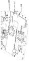
도 1 은 종래 기술에 따른 전자 디바이스의 분해도이다.
도 2 는 종래 기술에 따른 도 1 의 전자 디바이스의 부분 조립도이다.
도 3 은 도 1 및 도 2 의 종래 기술의 전자 디바이스에 대한 컴포넌트 대 히트싱크 연결의 확대 부분 단면도이다.
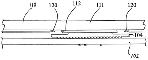
도 4a 및 도 4b 는 본 원리들의 구현들에 따른 전자 디바이스의 분해도들이다.
도 5 는 본 원리들의 구현에 따른, 도 4a 및 도 4b 의 전자 디바이스의 부분 조립도이다.
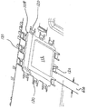
도 6 은 본 원리들의 구현에 따른, 전자 디바이스의 컴포넌트 실드의 개방 윈도우의 확대도이다.
도 7a 는 본 원리들의 구현에 따른, 완전히 조립된 전자 디바이스의 컴포넌트 실드에서의 개방 열 전달 윈도우의 확대 측면도를 도시한다.
도 7b 는 본 원리들의 상이한 구현에 따른, 완전히 조립된 전자 디바이스의 컴포넌트 실드에서의 개방 열 전달 윈도우의 확대 측면도를 도시한다.A more detailed understanding of the present invention may be obtained from the following description in conjunction with the accompanying drawings.
1 is an exploded view of an electronic device according to the prior art.
Figure 2 is a partial assembly view of the electronic device of Figure 1 in accordance with the prior art.
3 is an enlarged partial cross-sectional view of a component-to-heat sink connection for the prior art electronic device of FIGS. 1 and 2;
Figures 4A and 4B are exploded views of an electronic device according to embodiments of the present principles.
Figure 5 is a partial assembly view of the electronic device of Figures 4A and 4B, in accordance with an implementation of the present principles.
6 is an enlarged view of an open window of a component shield of an electronic device, in accordance with an implementation of the present principles.
Figure 7A shows an enlarged side view of an open heat transfer window in a component shield of a fully assembled electronic device, in accordance with an implementation of the present principles.
Figure 7B shows an enlarged side view of an open heat transfer window in a component shield of a fully assembled electronic device, in accordance with a different implementation of the present principles.
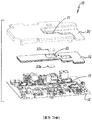
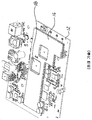
도 1 에 도시된 바와 같이, 종래 기술의 전자 디바이스 (10) 는 인쇄 회로 보드 (PCB) (12), 실드 (16) 및 히트싱크 또는 열 확산기 (20) 로 이루어진다. PCB (12) 는 다수의 컴포넌트들을 포함하며, 그들 중 일부는 다른 것들보다 더 많은 열을 생성하고 히트싱크들이 동작 동안 그 열의 소산을 도울 것을 요구한다. 그러한 컴포넌트들의 하나의 예는 도 4a 및 도 4b 에서 참조 번호 104 로서 식별된다.1, a prior art electronic device 10 comprises a printed circuit board (PCB) 12, a
일반적으로 말해서, 당업자들은 실드 (16) 가 여러 가지 이유들로 PCB 상의 다른 컴포넌트들로부터 PCB 컴포넌트들의 부분을 차폐하도록, 그러나 주로 실드 내에 포함된 컴포넌트들로부터 주위의 컴포넌트들로 방사하는 것으로부터, 또는 실드 내의 이들 컴포넌트들에 영향으로 미치는 것으로부터 실드 밖의 컴포넌트들에 의해 생성된 무선 주파수 간섭을 차폐하도록 구성된다는 것을 인정할 것이다. 이러한 무선 주파수 간섭 (RFI) 은 또한 통상 전자기 간섭 또는 EMI 로서 지칭된다.Generally speaking, those skilled in the art will appreciate that the
하나의 구현에 따르면, 본 원리들의 전자 디바이스는 각각의 컨텐츠 제공자들을 통해 고객들에게 일반적으로 제공되는 셋 톱 박스일 것이다. 다른 구현들에서, 본 원리들의 전자 디바이스는 각각 고객 또는 컨텐츠 소스 제공자로 또는 로부터 컨텐츠의 송신을 돕기 위해 사용되는 게이트웨이 디바이스일 수 있다. 당업자들은 다수의 상이한 타입들의 전자 디바이스들로의 본 원리들의 다른 구현들이 동일한 것의 의도된 범위로부터 일탈하지 않고 행해질 수 있다는 것을 인정할 것이다.According to one implementation, the electronic device of the present principles will be a set top box generally provided to customers through respective content providers. In other implementations, the electronic device of the present principles may be a gateway device, respectively, used to assist in the transmission of content to or from a customer or content source provider. Those skilled in the art will appreciate that other implementations of the present principles to a number of different types of electronic devices can be made without departing from the intended scope of the same.
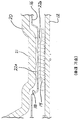
도 1 내지 도 3 을 참조하면, 실드 (16) 는 열 소산을 요구하는 컴포넌트들 (14) 위에 위치되는 하나 이상의 엠보스먼트들 (embossments) (18) 을 포함한다. 열 (열적, 열 전도성) 패드들 (22A, 22B) 은 컴포넌트 (14) 로부터 히트싱크 (20) 로 열을 전달하기 위해 사용된다. 도 3 에 도시된 바와 같이, 열 패드 (22B) 의 하면은 컴포넌트 (14) 상에 직접 위치된다. 열 패드 (22B) 의 상면은 실드 (16) 의 엠보스먼트 (18) 와 직접적인 열 접촉에 있고, 상부 열 패드 (22A) 는 그것의 저면에서 엠보스먼트 (18) 와 직접 접촉하고 있고 상면에서 히트싱크 (20) 에서의 함몰부 (21) 와 적집 접촉하고 있다. 이러한 방식으로, 컴포넌트 (14) 에 의해 생성된 열은 열 패드 (22B), 엠보스먼트 (18), 및 열 패드 (22A) 를 통해 히트싱크 또는 열 확산기 (20) 로 전달된다. 이러한 기지의 설계가 컴포넌트들로부터의 열 전달를 위해 효과적이지만, 상당한 문제가 PCB 에 대한 히트싱크 (20) 의 적절한 그라운딩에서 발생한다. 그러한 그라운딩 문제들은 전자 디바이스의 동작의 다수의 양태들에 개입할 수 있으며, 가장 중요한 문제는 PCB 상의 전자 컴포넌트들의 하나 이상에 대한 손상이며, 궁극적으로 전자 디바이스 (10) 의 실패된 동작을 초래한다. 이들 문제들 중 하나는 ESD 또는 정전기 방전으로서 통상 지칭되는 것에 의해 초래된다.Referring to Figures 1-3, the
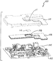
도 4a 및 도 4b 를 참조하면, 본 원리들의 구현에 따른 전자 디바이스 (100) 가 도시되어 있다. 전자 디바이스 (100) 는 인쇄 회로 보드 (PCB) (102), 실드 (106), 및 히트싱크 또는 열 확산기 (110) 로 이루어진다. 이러한 구현에서, 실드 (106) 는 컴포넌트 (104) 와 히트싱크 (110) 사이의 열-커플링이 만들어질 (이하에서 "열 전달 윈도우" 로서 지칭되는) 개방 윈도우 (108) 를 포함한다. 도 4a 는 열 패드 (112) 와 접촉하고 있는 표면 (111) 이 히트싱크 (110) 에서의 함몰부인 구현을 도시한다. 도 4b 는 표면 (111) 이 히트싱크 (110) 와 동일 평면인 (히트싱크 (110) 와 동일 레벨인, 히트싱크 (110) 와 동일한 수평 평면에 있는) 구현을 도시한다. 상이한 구현 (도시하지 않음) 에 따르면, 표면 (111) 은 히트싱크 (110) 로부터 돌출한다.Referring to Figures 4A and 4B, an
도 5 및 도 6 은 PCB (102) 상의 그것의 동작가능한 위치에 있는 실드 (106) 의 뷰를 도시한다. 도시된 바와 같이, 열 전달 윈도우 (108) 는 컴포넌트 (104) (도 4 및 도 7) 와 정렬되고, 열 패드 (112) 는 동일한 것 위에 위치된다. 실드 (106) 는 열 전달 윈도우 (108) 의 외주 주위에 위치된 복수의 그라운드 핑거들 (120) 을 포함할 수 있다. 그라운드 핑거들 (120) 은 바이어싱된 스프링이고 실드 (106) 의 평면형 표면으로부터 상방으로 돌출하며, 히트싱크 (110) 에서의 함몰부 (111) 와 물리적으로 맞물리도록 구성된다. 그라운드 핑거들 (120) 의 상향 스프링 바이어스는 함몰부 (111) 를 통해, 실드 (106) 와 히트싱크 (110) 사이의 일관되고 정확한 물리적 및 전기적 접촉을 보장한다.Figures 5 and 6 show a view of the
도 7a 및 도 7b 는 본 원리들의 상이한 구현들에 따른, 조립된 전자 디바이스의 컴포넌트 실드에서의 개방 열 전달 윈도우의 측면도를 도시한다. 도 7a 에 도시된 바와 같이, (히트싱크에서의 함몰부에 의해 마크된) 히트싱크 (110) 의 표면 (111) 은 개방 열 전달 윈도우 (108) 위에 위치되고 컴포넌트 (104) 상에 위치된 열 패드 (112) 와 직접 접촉한다. 도 7b 에 도시된 바와 같이, 히트싱크 (110) 의 (열 패드 (112) 가 히트싱크와 접촉하는 히트싱크의 하면상의 표면을 나타내는 파선에 의해 마크된) 표면 (111) 은 실드 (106) 에서의 개방 열 전달 윈도우 (108) 위에 위치되고, 열 패드 (112) 의 상부 표면이 실드 (106) 에서의 개방 열 전달 윈도우 (108) 와 거의 동일 레벨이거나 개방 열 전달 윈도우 (108) 로부터 약간 돌출 (위로 연장) 하기 때문에 컴포넌트 (104) 상에 위치된 열 패드 (112) 와 직접 접촉한다. 본 원리들의 또 다른 구현 (도시하지 않음) 에 따르면, 실드 (106) 에서의 개방 열 전달 윈도우 (108) 위에 위치되는 히트싱크 (110) 의 표면 (111) 은 실드 (106) 에서의 개방 열 전달 윈도우 (108) 로부터 돌출하는 열 패드 (112) 에 기인하여 히트싱크롤부터 돌출한다. 히트싱크 (110) 는 도 7a 에 도시된 바와 같이 형성될 수 있고, 따라서 열 패드 (112) 가 실드 (106) 로부터 돌출하지 않더라도 표면 (111) 에서의 엠보스먼트를 포함한다. 히트싱크 (110) 의 그러한 형태는 그것이 히트싱크 (110) 와 실드 (106) 사이의 거리를 증가시켜 히트싱크 (110) 주위의 공기흐름을 향상시킴으로써, 인쇄 회로 보드상의 컴포넌트들 및 실드 (106) 로의 히트싱크 (110) 의 열 전달을 감소시키면서 컴포넌트 (104) 로부터 열을 빼내는 히트싱크 (110) 의 능력을 더욱 개선하기 때문에 이로울 수도 있다. 따라서, 이러한 열-커플링 및 이것에 의해 히트싱크 (110) 로의 컴포넌트 (104) 의 열 전도성이 개선되는 것이 분명할 것이다. 이러한 설계는 그렇지 않은 경우 이러한 열-커플링에 영향을 주도록 열 경로에 존재할 실드층 (즉, 금속판의 층) 및 하나의 열 패드를 제거함으로써 종래기술의 그것보다 더 효율적인 열 전달을 제공한다. 실제로, 도 1 에 따른 종래 기술의 전자 디바이스 (10) 에서, 실드 (16) 는 컴포넌트 (14) 와 히트싱크 (20) 사이의 열 커플링에 포함되고, 컴포넌트 (14) 에 의해 가열될 것이며, 따라서 실드 (16) 바로 아래의 그리고 실드 (16) 의 외측 경계들에 가까운 PCB (12) 상의 다른 컴포넌트들로 열을 방사할 것이기 때문에, 이것은 원해지지 않고, 이것은 이들 다른 컴포넌트들의 기능에 그리고 일반적으로 전자 디바이스 (10) 의 기능에 해로울 수 있다.Figures 7A and 7B show a side view of an open heat transfer window in a component shield of an assembled electronic device, in accordance with different embodiments of the present principles. 7A, the
중요하게는, 히트싱크 (110) 에 실드 (106) 를 물리적으로 그리고 전기적으로 커플링하는 열 전달 윈도우 (108) 의 외주 주위의 그라운드 핑거들 (120) 을 갖는 개방 열 전달 윈도우를 갖는 본 원리는 실드가 컴포넌트 (104) 와 히트싱크 (110) 사이의 열 커플링에 포함되는 것을 회피한다. 이러한 방식으로, 히트싱크 (110) 의 그라운딩 및 PCB 상의 다른 컴포넌들로 실드의 열 방사와 연관된 상술된 문제들은 제거되고, 히트 싱크는 이제 실드 (106) 의 그라운드 핑거들 (120) 을 통해 PCB 에 충분히 그라운딩된다. 또, 일단 조립되면, 윈도우 (108) 에 의해 생성되는 차폐에서의 임의의 잠재적인 손실들은 히트싱크가 그라운딩되고 개방 열 전달 윈도우에 의해 형성된 영역을 폐쇄하기 때문에 윈도우 (108) 위에 위치되는 표면 (111) 을 갖는 히트싱크에 의해 제거된다. 당업자들은 히트싱크의 금속의, 전기적으로 전도성인 바디 (body) 가 개방 열 전달 윈도우 (108) 를 기능적으로 폐쇄한다는 것을 인정할 것이다. 개선된 차폐를 제공하는 구현를 위해, 그라운드 핑거들 (120) 은 해로운 것으로 여겨질 수 있는 파장 범위의 선택된 최대 파장보다 더 큰 갭들을 방지하기 위해 함께 충분히 가깝게 이격되며, 이것에 의해 그 간격 사이즈 위의 방사의 방사 파장들을 실드 (106) 및 개방 열 전달 윈도우 (108) 주위의 갭을 통과하는 것으로부터 효과적으로 감쇠시키거나 차단시킨다. 도 6 은 선택된 최대 파장에 기초하여 실드의 원하는 차폐 효과를 유지하도록 선택된 인접한 그라운드 핑거들 (120) 사이의 간격 (600) 의 예를 도시한다. 예시로써, 특정의 파장의 1/10 에서의 애퍼쳐 (aperture) 가 그 애퍼쳐에 입사하는 그 파장의 방사선의 90% 를 감쇠시키거나 차단하고 그 파장 위의 90% 보다 더 많이 감쇠시킬 것인 일반적인 규칙이 적용될 수 있다. 당업자들은 상기 예에서 사용되는 바와 같은 "애퍼쳐" 는 인접한 그라운드 핑거들 (120) 사이의 간격 (600) 과 유사하다는 것을 인정할 것이다. 이와 같이, 동일한 개념들이 본 원리들에 적용된다. 실드와 히트싱크 사이의 그라운드 핑거들은 히트싱크에 실드를 연결하고, 이것에 의해 컴포넌트가 실드에서의 개방 열 전달 윈도우의 생성으로부터 초래되는 외부로의 무선 주파수 방사를 누설시키는 것을 방지하면서 외부로부터의 전자기 간섭 및 정전기 방전에 대해 컴포넌트를 보호한다.Importantly, the present principles with an open heat transfer window having
당업자들은 그라운드 핑거들 (120) 의 물리적 형태가 그러한 핑거들이 대응하는 히트싱크/열 확산기와 양호한 물리적 및 전기적 연결을 일관성있게 행하도록 구성된다면, 본 원리들의 의도된 범위로부터 일탈하지 않고 도면들에 도시된 것과는 상이할 수도 있다는 것을 인정할 것이다. 하나의 바람직한 구현에서, 그라운드 핑거들 (120) 은 전자 디바이스를 조립할 때 히트싱크 (110) 가 그러한 스프링 바이어스에 대해 하방으로 강제되도록 상방으로 바이어싱된 스프링이며, 따라서 적절한 물리적 및 전기적 접촉을 보장한다.Those skilled in the art will appreciate that the physical form of the
상술한 것은 본 원리들을 실시하기 위한 가능성들의 일부를 설명한다. 다수의 다른 실시형태들이 본 원리들의 범위 및 사상 내에서 가능하다. 따라서, 상기의 설명은 제한보다는 예시적인 것으로서 간주되는 것 그리고 본 원리들의 범위는 그들의 정체 범위의 등가물들과 함께 첨부된 청구범위에 의해 주어지는 것이 의도된다.The foregoing describes some of the possibilities for implementing these principles. Many other embodiments are possible within the scope and spirit of these principles. Accordingly, the above description is intended to be regarded as illustrative rather than limiting, and the scope of the present principles is intended to be given by the appended claims along with their equivalents.
Claims (10)
상기 인쇄 회로 보드의 적어도 부분에 위치되도록 구성되고 열 소산을 요구하는 상기 하나 이상의 전자 컴포넌트들 위에 위치된 하나 이상의 개방 열 전달 윈도우들 (108) 을 갖는 실드 (106); 및
상기 실드에서의 상기 하나 이상의 개방 열 전달 윈도우들 위에 위치되도록 구성된 하나 이상의 표면들 (111) 을 갖는 히트싱크 (110) 를 포함하는, 전자 디바이스.An electronic device having a printed circuit board (102) having one or more electronic components (104) requiring heat dissipation,
A shield (106) configured to be positioned on at least a portion of the printed circuit board and having one or more open heat transfer windows (108) positioned over the one or more electronic components requiring heat dissipation; And
And a heat sink (110) having one or more surfaces (111) configured to be positioned over the at least one open heat transfer windows in the shield.
열 소산을 요구하는 상기 하나 이상의 컴포넌트들상에 직접 위치된 일측면을 갖는 하나 이상의 열 패드들 (112) 을 더 포함하고,
상기 히트싱크의 상기 하나 이상의 표면들은 상기 실드에서의 상기 하나 이상의 개방 열 전달 윈도우들을 통해 상기 하나 이상의 열 패드들의 대향하는 측면과 물리적으로 접촉하는, 전자 디바이스.The method according to claim 1,
Further comprising one or more thermal pads (112) having a side positioned directly on said one or more components requiring heat dissipation,
Wherein the one or more surfaces of the heat sink are in physical contact with opposing sides of the one or more heat pads through the one or more open heat transfer windows in the shield.
상기 실드는 상기 하나 이상의 개방 열 전달 윈도우들 주위에 위치된 하나 이상의 핑거들 (120) 을 포함하고,
하나 이상의 핑거들은 상기 히트싱크의 상기 하나 이상의 표면들이 상기 실드에서의 상기 하나 이상의 개방 열 전달 윈도우들 위에 위치되는 경우 상기 실드에 대한 상기 히트싱크와의 물리적 및 전기적 연결을 행하도록 구성되는, 전자 디바이스. 3. The method according to claim 1 or 2,
Wherein the shield comprises one or more fingers (120) positioned around the at least one open heat transfer windows,
Wherein the one or more fingers are configured to make a physical and electrical connection to the heat sink for the shield when the one or more surfaces of the heat sink are located above the one or more open heat transfer windows in the shield. .
상기 하나 이상의 핑거들은 상기 실드에서의 상기 하나 이상의 개방 열 전달 윈도우들의 외주 주위에 위치된 하나 이상의 핑거들을 포함하는, 전자 디바이스.The method of claim 3,
Wherein the one or more fingers comprise one or more fingers positioned about an outer circumference of the one or more open heat transfer windows in the shield.
상기 하나 이상의 핑거들은 상기 히트싱크의 상기 하나 이상의 표면들과 전기적 접촉을 보장하기 위해 상기 실드의 평면형 표면에 대해 상방으로 바이어싱되는, 전자 디바이스.5. The method of claim 4,
Wherein the one or more fingers are biased upward relative to the planar surface of the shield to ensure electrical contact with the one or more surfaces of the heat sink.
상기 하나 이상의 핑거들 사이에 간격 (600) 을 더 포함하고,
상기 간격은 상기 실드에 의해 차단될 무선 주파수 파장들에 기초하는, 전자 디바이스.The method of claim 3,
Further comprising an interval (600) between the one or more fingers,
Wherein the interval is based on radio frequency waves to be blocked by the shield.
상기 간격은 상기 실드에 의해 차단될 상기 무선 주파수 파장들의 최대값의 적어도 1/10 인, 전자 디바이스.The method according to claim 6,
Wherein the spacing is at least one-tenth of a maximum value of the radio frequency waves to be shielded by the shield.
상기 하나 이상의 표면들은 상기 히트싱크에서 하나 이상의 함몰부들을 제공하도록 구성되는, 전자 디바이스.3. The method according to claim 1 or 2,
Wherein the one or more surfaces are configured to provide one or more depressions in the heat sink.
상기 하나 이상의 표면들은 상기 히트싱크와 동일 평면이도록 구성되는, 전자 디바이스.3. The method according to claim 1 or 2,
Wherein the one or more surfaces are configured to be flush with the heat sink.
상기 하나 이상의 표면들은 상기 히트싱크로부터 돌출하도록 구성되는, 전자 디바이스.3. The method according to claim 1 or 2,
Wherein the one or more surfaces are configured to protrude from the heat sink.
Applications Claiming Priority (2)
| Application Number | Priority Date | Filing Date | Title |
|---|---|---|---|
| US14/978,682 | 2015-12-22 | ||
| US14/978,682 US20170181266A1 (en) | 2015-12-22 | 2015-12-22 | Electronic circuit board shielding with open window heat transfer path |
Publications (1)
| Publication Number | Publication Date |
|---|---|
| KR20170074806A true KR20170074806A (en) | 2017-06-30 |
Family
ID=57570009
Family Applications (1)
| Application Number | Title | Priority Date | Filing Date |
|---|---|---|---|
| KR1020160175703A KR20170074806A (en) | 2015-12-22 | 2016-12-21 | Electronic circuit board shielding with open window heat transfer path |
Country Status (6)
| Country | Link |
|---|---|
| US (1) | US20170181266A1 (en) |
| EP (1) | EP3185665A1 (en) |
| JP (1) | JP2017135368A (en) |
| KR (1) | KR20170074806A (en) |
| CN (1) | CN106961824A (en) |
| BR (1) | BR102016030323A2 (en) |
Families Citing this family (12)
| Publication number | Priority date | Publication date | Assignee | Title |
|---|---|---|---|---|
| EP3756431A1 (en) | 2018-02-19 | 2020-12-30 | InterDigital CE Patent Holdings | Heatsink assembly for an electronic device |
| WO2019236523A1 (en) * | 2018-06-05 | 2019-12-12 | Plume Design, Inc. | Compact, direct plugged, and high-performance wi-fi access point |
| JP7107766B2 (en) * | 2018-06-26 | 2022-07-27 | デクセリアルズ株式会社 | Electronics |
| WO2020235647A1 (en) * | 2019-05-23 | 2020-11-26 | 株式会社ソニー・インタラクティブエンタテインメント | Electronic device |
| KR102651418B1 (en) * | 2019-07-25 | 2024-03-27 | 삼성전자 주식회사 | Electronic device including a shielding sheet and a heat radiation member |
| US11369051B2 (en) | 2019-07-26 | 2022-06-21 | Samsung Electronics Co., Ltd. | Electromagnetic interference (EMI) shielding member and electronic device including the same |
| CN112399768B (en) * | 2019-08-13 | 2023-05-12 | Oppo广东移动通信有限公司 | Shielding cover, circuit board assembly and electronic equipment |
| US11348877B2 (en) * | 2019-12-10 | 2022-05-31 | Starry, Inc. | RF shielding can with integral spring fingers |
| JP2021174847A (en) * | 2020-04-23 | 2021-11-01 | 株式会社デンソー | Electronic device |
| TWI743941B (en) * | 2020-08-12 | 2021-10-21 | 啟碁科技股份有限公司 | Electronic device and heat dissipated emi shielding structure |
| US11647609B2 (en) * | 2020-12-15 | 2023-05-09 | Arris Enterprises Llc | Multisided heat spreader |
| WO2023199608A1 (en) * | 2022-04-11 | 2023-10-19 | 株式会社ソニー・インタラクティブエンタテインメント | Electronic apparatus |
Family Cites Families (22)
| Publication number | Priority date | Publication date | Assignee | Title |
|---|---|---|---|---|
| JPH0582994A (en) * | 1991-09-20 | 1993-04-02 | Fujitsu Ltd | Box type unit structure |
| US5530202A (en) * | 1995-01-09 | 1996-06-25 | At&T Corp. | Metallic RF or thermal shield for automatic vacuum placement |
| JPH08288687A (en) * | 1995-04-14 | 1996-11-01 | Nec Corp | Shield structure of printed board |
| JPH0927576A (en) * | 1995-07-11 | 1997-01-28 | Nec Corp | Package for semiconductor integrated circuit |
| US5724234A (en) * | 1996-05-02 | 1998-03-03 | Ericsson Inc. | Slotted shield can |
| JP3313682B2 (en) * | 1999-11-18 | 2002-08-12 | 北川工業株式会社 | Electromagnetic wave shield case |
| US6445583B1 (en) * | 2001-01-26 | 2002-09-03 | Laird Technologies, Inc. | Snap in heat sink shielding lid |
| US6744640B2 (en) * | 2002-04-10 | 2004-06-01 | Gore Enterprise Holdings, Inc. | Board-level EMI shield with enhanced thermal dissipation |
| JP2004327841A (en) * | 2003-04-25 | 2004-11-18 | Sony Corp | Electronic apparatus |
| TW200522856A (en) * | 2003-12-30 | 2005-07-01 | Asustek Comp Inc | Electronic apparatus and shielding device thereof |
| US7254034B2 (en) * | 2004-12-15 | 2007-08-07 | Lucent Technologies Inc. | Thermal management for shielded circuit packs |
| US20070090509A1 (en) * | 2005-10-14 | 2007-04-26 | Oqo, Inc. | Electromagnetic interference circuit package shield |
| CN1953646A (en) * | 2005-10-18 | 2007-04-25 | 鸿富锦精密工业(深圳)有限公司 | Heat radiator capable of preventing electromagnetic interference |
| US20090091888A1 (en) * | 2007-10-09 | 2009-04-09 | Chao-Chun Lin | Emi shielding and heat dissipating structure |
| TWI370722B (en) * | 2008-12-22 | 2012-08-11 | Unihan Corp | Electromagnetic shielding device with heat dissipating |
| JP2011176096A (en) * | 2010-02-24 | 2011-09-08 | Mitsumi Electric Co Ltd | Electronic apparatus |
| US9030841B2 (en) * | 2012-02-23 | 2015-05-12 | Apple Inc. | Low profile, space efficient circuit shields |
| CN202663712U (en) * | 2012-04-26 | 2013-01-09 | 鸿富锦精密工业(深圳)有限公司 | Electromagnetic shielding device with heat radiation function |
| US9439333B2 (en) * | 2013-01-15 | 2016-09-06 | Genesis Technology Usa, Inc. | Heat-dissipating EMI/RFI shield |
| CN103929935A (en) * | 2013-01-15 | 2014-07-16 | 起源技术美国股份有限公司 | Radiating Emi/rfi Shielding Device |
| JP6000170B2 (en) * | 2013-03-15 | 2016-09-28 | 三菱電機株式会社 | Electronics |
| EP2933833A1 (en) * | 2014-04-16 | 2015-10-21 | Thomson Licensing | Electromagnetic shielding device |
-
2015
- 2015-12-22 US US14/978,682 patent/US20170181266A1/en not_active Abandoned
-
2016
- 2016-12-14 EP EP16204069.5A patent/EP3185665A1/en not_active Withdrawn
- 2016-12-15 JP JP2016243710A patent/JP2017135368A/en active Pending
- 2016-12-21 KR KR1020160175703A patent/KR20170074806A/en not_active Application Discontinuation
- 2016-12-22 CN CN201611204492.1A patent/CN106961824A/en active Pending
- 2016-12-22 BR BR102016030323-0A patent/BR102016030323A2/en active Search and Examination
Also Published As
| Publication number | Publication date |
|---|---|
| US20170181266A1 (en) | 2017-06-22 |
| JP2017135368A (en) | 2017-08-03 |
| CN106961824A (en) | 2017-07-18 |
| EP3185665A1 (en) | 2017-06-28 |
| BR102016030323A2 (en) | 2017-06-27 |
Similar Documents
| Publication | Publication Date | Title |
|---|---|---|
| KR20170074806A (en) | Electronic circuit board shielding with open window heat transfer path | |
| JP4914678B2 (en) | Electronics | |
| US20170181265A1 (en) | Electronic circuit board shielding with open window heat transfer path | |
| US7924568B2 (en) | Heat sink device with a shielding member | |
| CN108370656B (en) | Sliding thermal barrier | |
| US20110235278A1 (en) | Circuit module | |
| WO2017143941A1 (en) | Heat dissipation component | |
| JP2006253657A (en) | Electromagnetic shielding structure | |
| JP2005159137A (en) | Optical semiconductor device and electronic apparatus using it | |
| TWI533793B (en) | Electronic device and electromagnetic wave shielding module thereof | |
| US6943436B2 (en) | EMI heatspreader/lid for integrated circuit packages | |
| US20190174659A1 (en) | Ciruit board assembly and shielding device | |
| US20040012939A1 (en) | EMI shielding apparatus | |
| CN113711160B (en) | Electronic device | |
| TWI713258B (en) | Signal transmission device | |
| JP7382750B2 (en) | electronic circuit module | |
| KR101305581B1 (en) | Shield member and pcb comprising the shield member | |
| KR100733386B1 (en) | Printed circuit board for intercepting electro magnetic and preventing electro-static and manufactutring method thereof | |
| JP7419661B2 (en) | board module | |
| JP2011222543A (en) | Electronic device | |
| WO2019000162A1 (en) | Electromagnetic shielding for electronic device | |
| JP2018022744A (en) | Electronic device | |
| TW201601612A (en) | Electronic device with protection shield | |
| JPH0513972A (en) | Heat dissipating mounting structure of heat releasing part |
Legal Events
| Date | Code | Title | Description |
|---|---|---|---|
| A201 | Request for examination | ||
| E902 | Notification of reason for refusal |