KR20170063243A - Organic light emitting diode display - Google Patents
Organic light emitting diode display Download PDFInfo
- Publication number
- KR20170063243A KR20170063243A KR1020150169389A KR20150169389A KR20170063243A KR 20170063243 A KR20170063243 A KR 20170063243A KR 1020150169389 A KR1020150169389 A KR 1020150169389A KR 20150169389 A KR20150169389 A KR 20150169389A KR 20170063243 A KR20170063243 A KR 20170063243A
- Authority
- KR
- South Korea
- Prior art keywords
- electrode
- light emitting
- organic light
- dummy
- auxiliary
- Prior art date
- Legal status (The legal status is an assumption and is not a legal conclusion. Google has not performed a legal analysis and makes no representation as to the accuracy of the status listed.)
- Granted
Links
Images


Classifications
-
- H01L51/5203—
-
- H01L27/326—
-
- H01L51/5212—
-
- H01L51/5228—
-
- H01L51/56—
-
- H01L2227/32—
Landscapes
- Electroluminescent Light Sources (AREA)
Abstract
본 발명의 일 실시예에 따른 보조전극과 더미전극이 있는 유기 발광 표시 장치가 제공된다. 표시영영과 비표시영역이 정의된 기판상에 유기 발광 소자가 배치된다. 보조전극과 유기 발광 소자는 표시영역에 배치되고, 표시영역을 덮으며 비표시영역의 적어도 일부를 덮도록 배치된 공통전극이 배치된다. 보조전극과 더미전극은 공통전극의 전기적 저항을 낮추도록 공통전극과 연결된다. 더미전극은 비표시영역에 배치되어 표시영역에 제한적으로 배치된 보조전극의 전류 흐름성을 공통전극과 연결된 더미전극에 의해 개선되어 유기 발광 표시 장치의 휘도를 균일하게 할 수 있다.There is provided an organic light emitting diode display having an auxiliary electrode and a dummy electrode according to an embodiment of the present invention. An organic light emitting element is disposed on a substrate on which a display area and a non-display area are defined. The auxiliary electrode and the organic light emitting element are disposed in a display region, and a common electrode disposed to cover at least a part of the non-display region is disposed. The auxiliary electrode and the dummy electrode are connected to the common electrode so as to lower the electrical resistance of the common electrode. The dummy electrode is improved by the dummy electrode disposed in the non-display region and connected to the common electrode so that the current flowability of the auxiliary electrode which is limitedly disposed in the display region can be made uniform.
Description
본 발명은 유기 발광 표시 장치에 관한 것으로서, 보다 상세하게는 보조전극을 포함하는 유기 발광 표시 장치에 있어 더미전극을 통해 전류의 흐름을 원활히 하여 휘도를 더욱 균일하게 유지 할 수 있는 유기 발광 표시 장치를 제공하는 것이다.The present invention relates to an organic light emitting diode (OLED) display, and more particularly, to an organic light emitting diode (OLED) display device including an auxiliary electrode, which can smoothly flow current through a dummy electrode, .
유기 발광 표시 장치(OLED)는 자체 발광형 표시 장치로서, 전자(electron) 주입을 위한 전극(cathode)과 정공(hole) 주입을 위한 전극(anode)으로부터 각각 전자와 정공을 발광층 내부로 주입시켜, 주입된 전자와 정공이 결합한 엑시톤(exciton)이 여기 상태로부터 기저 상태로 떨어질 때 발광하는 유기 발광 소자를 이용한 표시 장치이다. The organic light emitting diode (OLED) is a self-luminous display device in which electrons and holes are injected into the light emitting layer from an anode for injecting electrons and an anode for injecting holes, And emits light when an exciton in which injected electrons and holes are coupled falls from an excited state to a ground state.
유기 발광 표시 장치는 빛이 방출되는 방향에 따라서 상부 발광(Top Emission) 방식, 하부 발광(Bottom Emission) 방식 및 양면 발광(Dual Emission) 방식 등이 있고, 구동 방식에 따라서는 수동 매트릭스형(Passive Matrix)과 능동 매트릭스형(Active Matrix) 등으로 나누어진다.The organic light emitting display device includes a top emission type, a bottom emission type, and a dual emission type depending on a direction in which light is emitted, and a passive matrix type ) And active matrix (Active Matrix).
유기 발광 표시 장치는 액정 표시 장치(LCD)와는 달리 별도의 광원이 필요하지 않아 경량 박형으로 제조 가능하다. 또한, 유기 발광 표시 장치는 저전압 구동에 의해 소비 전력 측면에서 유리할 뿐만 아니라, 색상 구현, 응답 속도, 시야각, 명암비(contrast ratio: CR)도 우수하여, 차세대 디스플레이로서 연구되고 있다.Unlike a liquid crystal display (LCD), an organic light emitting display does not require a separate light source, and can be manufactured in a light and thin shape. Further, the organic light emitting display device is not only advantageous from the viewpoint of power consumption by low voltage driving, but also excellent in color implementation, response speed, viewing angle, and contrast ratio (CR), and is being studied as a next generation display.
고 해상도로 디스플레이가 발전하면서 단위 면적당 픽셀 개수가 증가하고, 높은 휘도가 요구되고 있지만 유기 발광 표시 장치의 발광 구조 상 단위 면적의 휘도(Cd)에 한계가 있고, 인가 전류의 증가로 인한 유기 발광 소자의 신뢰성 저하 및 소비 전력이 증가하는 문제점이 있다. The number of pixels per unit area increases and a high luminance is required. However, the luminance (Cd) of a unit area of the organic light emitting display device is limited by the light emitting structure, There is a problem in that the reliability of the battery and the power consumption increase.
따라서 유기 발광 표시 장치의 품질 및 생산성을 저해하는 요인이 되고 있는 유기 발광 소자의 발광 효율, 수명 향상 및 소비 전력 절감이라는 기술적 한계를 극복해야 하며, 색감 영역을 유지하면서도 발광 효율, 발광층의 수명 및 시야각 특성을 향상시킬 수 있는 유기 발광 소자 개발을 위한 다양한 연구가 이루어지고 있다.Therefore, it is necessary to overcome the technical limitations of the luminous efficiency, life span and power consumption reduction of the organic light emitting device, which are factors that hinder the quality and productivity of the OLED display device. Various studies have been conducted for developing an organic light emitting device capable of improving characteristics.
유기 발광 표시 장치(OLED)는 서로 대향하여 위치하는 화소전극(애노드, anode) 및 공통전극(캐소드, cathode) 사이에 형성된 유기 발광층을 포함하며 화소전극은 각각의 서브 화소 영역에 대응하도록 형성되고, 공통전극은 복수 개의 서브 화소 영역에 공통으로 대응하도록 형성된다.The organic light emitting diode OLED includes an organic light emitting layer formed between a pixel electrode (anode) and a common electrode (cathode) positioned opposite to each other and the pixel electrode is formed to correspond to each sub pixel region, The common electrode is formed to correspond to a plurality of sub pixel regions in common.
이와 같이, 각각의 서브 화소 영역에 대응하도록 형성되는 화소전극과 다르게, 공통전극은 복수 개의 서브 화소 영역 전체에 대응하도록 형성됨에 따라 화소전극에 비해 높은 저항을 갖는다. As described above, unlike the pixel electrodes formed so as to correspond to the respective sub-pixel regions, the common electrode is formed to correspond to all of the plurality of sub-pixel regions, and thus has a higher resistance than the pixel electrodes.
특히, 유기 발광 표시 장치가 공통전극을 투과하는 경로로 광을 방출하는 상부 발광 방식의 유기 발광 표시 장치인 경우에, 표시영역에서의 휘도를 높이기 위하여, 공통전극은 되도록 얇은 두께의 투명 도전성 재료로 형성되나, 이에 따라 공통전극은 더 높은 저항을 가질 수 있다.Particularly, in the case of an organic light emitting display device of a top emission type in which an organic light emitting display device emits light in a path passing through a common electrode, in order to increase the luminance in the display area, the common electrode is made of a transparent conductive material So that the common electrode can have a higher resistance.
상술한 바와 같이 공통전극의 높은 저항으로 인해 유기 발광 표시 장치의 표시영역의 중심부에서 전압 강하 현상이 발생하여 표시영역의 휘도 균일도가 저하되는 문제점이 있다. 또한, 원하는 수준의 휘도를 확보하기 위해서는 유기 발광 표시 장치의 소비 전력이 상승하는 문제점이 있다.As described above, due to the high resistance of the common electrode, a voltage drop phenomenon occurs at the center of the display region of the organic light emitting diode display, resulting in a problem that luminance uniformity of the display region is lowered. In addition, there is a problem that the power consumption of the organic light emitting display device is increased in order to secure a desired level of luminance.
이러한 문제점을 해소하기 위하여, 유기 발광 표시 장치는 공통전극의 저항을 낮추기 위하여 공통전극보다 낮은 저항을 갖는 재료로 형성되는 별도의 보조 전극을 더 포함할 수 있다.In order to solve this problem, the organic light emitting display may further include a separate auxiliary electrode formed of a material having a lower resistance than the common electrode in order to lower the resistance of the common electrode.
보조 전극과 공통전극을 서로 전기적으로 연결하기 위하여 보조 전극 컨택 영역에 레이저(Laser)를 조사함으로써 순간적인 레이저의 열 에너지로 금속으로 이루어진 전극 물질을 녹여 보조 전극과 공통전극 사이에 컨택(contact)을 형성할 수 있다. In order to electrically connect the auxiliary electrode and the common electrode to each other, a laser is irradiated to the auxiliary electrode contact region to dissolve the electrode material made of metal with the thermal energy of the instantaneous laser, and a contact is made between the auxiliary electrode and the common electrode .
또는, 보조 전극과 공통전극을 서로 전기적으로 연결하기 위한 언더컷 구조의 평탄층을 사용하여, 유기 발광층과 공통전극간의 스탭 커버리지(Step coverage)차이에 의해 언더컷의 내부에 위치한 보조전극으로 공통전극이 배치되어 컨택함으로써 전기적으로 연결되는 방법을 사용할 수 도 있다.Alternatively, the common electrode may be disposed as an auxiliary electrode located inside the undercut by a step coverage difference between the organic light emitting layer and the common electrode using a flat layer of an undercut structure for electrically connecting the auxiliary electrode and the common electrode to each other. So that they can be electrically connected to each other.
이와 같이 공통전극의 전기저항을 낮추어 균일한 휘도를 유지하기 위한 보조전극은 표시영역(active area) 내부의 화소와 화소 사이 제한적인 공간에 좁게 배치될 수 밖에 없다. 유기 발광 표시 장치의 외곽으로 갈수록 누적된 전류량이 증가하며 전압 강하(IR Drop) 현상이 증가하고 휘도는 감소하게 된다. As described above, the auxiliary electrode for maintaining the uniform luminance by lowering the electric resistance of the common electrode can only be arranged narrowly in a limited space between the pixels in the active area and the pixels. The amount of current accumulated increases toward the outer periphery of the organic light emitting display device, the voltage drop (IR drop) phenomenon increases, and the luminance decreases.
즉, 유기 발광 표시 장치의 회로부에서 제공되는 전류는 화소전극, 유기 발광 소자 및 공통전극을 통하여 흘러가게 되는데 공급량을 균일하게 유지하여 휘도를 균일하게 유지하는 것과 마찬가지로 전류의 흐름성을 개선하여 휘도를 개선하여야 하는 문제점이 있었다.That is, the current supplied from the circuit portion of the organic light emitting display device flows through the pixel electrode, the organic light emitting diode, and the common electrode. The current is uniformly maintained by maintaining the supply amount uniformly, There has been a problem that it should be improved.
본 발명의 실시예에 따른 해결 과제는, 유기 발광 표시 장치에 있어서, 보조 전극을 통한 전류의 흐름성을 원활하게 하는 더미전극을 사용하여 휘도 편차를 최소화할 수 있는 유기 발광 표시 장치를 제공하는 것을 목적으로 한다.An object of the present invention is to provide an organic light emitting diode (OLED) display device capable of minimizing a luminance deviation by using a dummy electrode that smoothes current flow through an auxiliary electrode in an organic light emitting display The purpose.
본 발명의 실시예에 따른 해결 과제들은 이상에서 언급한 과제들로 제한되지 않으며, 언급되지 않은 또 다른 과제들은 아래의 기재로부터 당업자에게 명확하게 이해될 수 있을 것이다.The solutions according to the embodiments of the present invention are not limited to the above-mentioned problems, and other problems not mentioned can be clearly understood by those skilled in the art from the following description.
본 발명의 일 실시예에 따른 전류의 흐름이 원활하도록 더미전극이 있는 유기 발광 표시 장치가 제공된다. 기판상에 복수의 유기 발광 소자와 보조전극이 있고, 유기 발광 소자에 있는 공통전극의 전기저항을 낮추도록 보조전극과 공통전극은 전기적으로 연결된다. 유기 발광 소자 및 보조전극을 통한 전류의 흐름이 원활하도록 더미전극을 기판상에 배치하고 공통전극과 더미전극을 연결하여 공통전극의 전기저항을 낮춤과 동시에, 유기 발광 소자로부터 보조전극을 통하는 전류의 흐름성은 낮은 전기저항을 갖고 전류 전도도가 높은 더미전극에 의해 향상될 수 있다.An organic light emitting display device having a dummy electrode is provided to facilitate current flow according to an embodiment of the present invention. A plurality of organic light emitting elements and an auxiliary electrode are provided on the substrate, and the auxiliary electrode and the common electrode are electrically connected to each other to lower the electric resistance of the common electrode in the organic light emitting element. The dummy electrode is disposed on the substrate so that current flows smoothly through the organic light emitting diode and the auxiliary electrode, and the common electrode and the dummy electrode are connected to each other to reduce the electric resistance of the common electrode. Flowability can be improved by a dummy electrode with low electrical resistance and high current conductivity.
공통전극은 투명 도전성 물질로 이루어질 수 있다.The common electrode may be made of a transparent conductive material.
더미전극은 보조전극과 연결될 수 있다.The dummy electrode may be connected to the auxiliary electrode.
보조전극보다 더미전극의 전기저항이 낮을 수 있다.The electric resistance of the dummy electrode may be lower than that of the auxiliary electrode.
보조전극보다 더미전극은 전기저항이 낮은 금속으로 이루어질 수 있다.The dummy electrode may be made of a metal having a lower electrical resistance than the auxiliary electrode.
보조전극보다 더미전극의 폭이 넓을 수 있다.The width of the dummy electrode may be larger than that of the auxiliary electrode.
더미전극은 기판상에 정의된 비표시영역에 있을 수 있다.The dummy electrode may be in a non-display area defined on the substrate.
더미전극은 표시영역의 외곽을 둘러쌓을 수 있다.The dummy electrode can surround the periphery of the display area.
더미전극과 보조전극은 각각 공통전극과 전기적으로 연결되는 적어도 하나의 연결부를 가질 수 있다.The dummy electrode and the auxiliary electrode may each have at least one connection portion electrically connected to the common electrode.
연결부는 레이저를 사용한 웰딩방식의 연결부일 수 있다.The connection may be a welded connection using a laser.
연결부는 언더컷 구조가 있는 연결부일 수 있다.The connection may be a connection with an undercut structure.
더미전극과 보조전극은 전기적으로 연결될 수 있다.The dummy electrode and the auxiliary electrode may be electrically connected.
본 발명의 일 실시예에 따른 유기 발광 표시 장치가 제공된다. 유기 발광 표시 장치는 유기 발광 소자들이 배열된 표시영역(active area)이 있는 기판 및 표시영역 내부에 배열된 화소들 사이에 열(column) 방향을 따라 연장된 보조전극들을 포함한다. 화소들 중 최외곽 화소들의 열을 따라 연장된 더미전극은 보조전극들에 비하여 폭이 더 크며 유기 발광 소자의 공통 전극과의 연결부가 더 많이 배치된다.An organic light emitting display according to an embodiment of the present invention is provided. The organic light emitting display includes a substrate having an active area in which organic light emitting devices are arranged, and auxiliary electrodes extending in a column direction between pixels arranged in the display area. The dummy electrode extending along the row of the outermost pixels among the pixels is larger in width than the auxiliary electrodes and more connected to the common electrode of the organic light emitting device.
연결부는 더미전극 또는 보조전극이 공통전극과 전기적으로 연결된 연결부일 수 있다.The connection portion may be a dummy electrode or a connection portion in which the auxiliary electrode is electrically connected to the common electrode.
연결부는 레이저를 사용한 웰딩방식에 의한 구조 또는 언더컷 구조일 수 있다.The connecting portion may be a structure by a welding method using a laser or an undercut structure.
더미전극은 표시영역의 상단 및 하단에 더 있으며 최외곽 화소들을 따라 연장되어 표시 영역을 둘러쌓을 수 있다.The dummy electrodes are further provided at the upper and lower ends of the display area and extend along the outermost pixels to surround the display area.
본 발명의 실시예에 따라 더미전극을 이용함으로써 휘도 균일도를 개선할 수 있는 효과가 있다. According to the embodiment of the present invention, luminance uniformity can be improved by using dummy electrodes.
또한, 본 발명의 실시예에 따라 더미전극을 구비함으로써 소비전력을 저감할 수 있는 효과가 있다.Further, according to the embodiment of the present invention, the provision of the dummy electrode has the effect of reducing power consumption.
본 발명의 효과는 이상에서 언급한 효과에 제한되지 않으며, 언급되지 않은 또 다른 효과는 아래의 기재로부터 당업자에게 명확하게 이해될 수 있을 것이다.The effects of the present invention are not limited to the effects mentioned above, and other effects not mentioned can be clearly understood by those skilled in the art from the following description.
이상에서 해결하고자 하는 과제, 과제 해결 수단, 효과에 기재한 발명의 내용이 청구항의 필수적인 특징을 특정하는 것은 아니므로, 청구항의 권리범위는 발명의 내용에 기재된 사항에 의하여 제한되지 않는다.The scope of the claims is not limited by the matters described in the contents of the invention, as the contents of the invention described in the problems, the solutions to the problems and the effects to be solved do not specify essential features of the claims.
도 1a는 본 발명의 일 실시예에 따른 전류 흐름성을 개선하도록 더미전극을 포함하는 유기 발광 표시 장치를 설명하기 위한 개략적인 평면도이다.
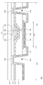
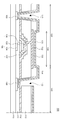
도 1b 내지 1c는 본 발명의 일 실시예에 따른 보조전극 및 더미전극과 공통전극간의 다양한 전기적 연결관계를 설명하기 위한 도 1a의 A-A'에 따른 개략적인 단면도이다.
도 2는 본 발명의 일 실시예에 따른 더미전극의 또다른 배치관계를 설명하기 위한 개략적인 평면도이다.FIG. 1A is a schematic plan view illustrating an OLED display including dummy electrodes to improve current flowability according to an exemplary embodiment of the present invention. Referring to FIG.
FIGS. 1B to 1C are schematic cross-sectional views taken along line A-A 'of FIG. 1A to explain various electrical connection relationships between the auxiliary electrode and the dummy electrode and the common electrode according to the embodiment of the present invention.
2 is a schematic plan view for explaining another arrangement relationship of dummy electrodes according to an embodiment of the present invention.
본 발명의 이점 및 특징, 그리고 그것들을 달성하는 방법은 첨부되는 도면과 함께 상세하게 후술되어 있는 실시예들을 참조하면 명확해질 것이다. 그러나 본 발명은 이하에서 개시되는 실시예들에 한정되는 것이 아니라 서로 다른 다양한 형태로 구현될 것이며, 단지 본 실시예들은 본 발명의 개시가 완전하도록 하며, 본 발명이 속하는 기술분야에서 통상의 지식을 가진 자에게 발명의 범주를 완전하게 알려주기 위해 제공되는 것이며, 본 발명은 청구항의 범주에 의해 정의될 뿐이다. BRIEF DESCRIPTION OF THE DRAWINGS The advantages and features of the present invention and the manner of achieving them will become apparent with reference to the embodiments described in detail below with reference to the accompanying drawings. The present invention may, however, be embodied in many different forms and should not be construed as being limited to the embodiments set forth herein. Rather, these embodiments are provided so that this disclosure will be thorough and complete, and will fully convey the scope of the invention to those skilled in the art. Is provided to fully convey the scope of the invention to those skilled in the art, and the invention is only defined by the scope of the claims.
본 발명의 실시예를 설명하기 위한 도면에 개시된 형상, 크기, 비율, 각도, 개수 등은 예시적인 것이므로 본 발명이 도시된 사항에 한정되는 것은 아니다. 명세서 전체에 걸쳐 동일 참조 부호는 동일 구성 요소를 지칭한다. 또한, 본 발명을 설명함에 있어서, 관련된 공지 기술에 대한 구체적인 설명이 본 발명의 요지를 불필요하게 흐릴 수 있다고 판단되는 경우 그 상세한 설명은 생략한다. 본 명세서 상에서 언급된 '포함한다', '갖는다', '이루어진다' 등이 사용되는 경우 '~만'이 사용되지 않는 이상 다른 부분이 추가될 수 있다. 구성 요소를 단수로 표현한 경우에 특별히 명시적인 기재 사항이 없는 한 복수를 포함하는 경우를 포함한다. The shapes, sizes, ratios, angles, numbers, and the like disclosed in the drawings for describing the embodiments of the present invention are illustrative, and thus the present invention is not limited thereto. Like reference numerals refer to like elements throughout the specification. In the following description, well-known functions or constructions are not described in detail since they would obscure the invention in unnecessary detail. Where the terms "comprises", "having", "done", and the like are used in this specification, other portions may be added unless "only" is used. Unless the context clearly dictates otherwise, including the plural unless the context clearly dictates otherwise.
구성 요소를 해석함에 있어서, 별도의 명시적 기재가 없더라도 오차 범위를 포함하는 것으로 해석한다.In interpreting the constituent elements, it is construed to include the error range even if there is no separate description.
위치 관계에 대한 설명일 경우, 예를 들어, '~상에', '~상부에', '~하부에', '~옆에' 등으로 두 부분의 위치 관계가 설명되는 경우, '바로' 또는 '직접'이 사용되지 않는 이상 두 부분 사이에 하나 이상의 다른 부분이 위치할 수도 있다.In the case of a description of the positional relationship, for example, if the positional relationship between two parts is described as 'on', 'on top', 'under', and 'next to' Or " direct " is not used, one or more other portions may be located between the two portions.
제1, 제2 등이 다양한 구성요소들을 서술하기 위해서 사용되나, 이들 구성요소들은 이들 용어에 의해 제한되지 않는다. 이들 용어들은 단지 하나의 구성요소를 다른 구성요소와 구별하기 위하여 사용하는 것이다. 따라서, 이하에서 언급되는 제1 구성요소는 본 발명의 기술적 사상 내에서 제2 구성요소일 수도 있다.The first, second, etc. are used to describe various components, but these components are not limited by these terms. These terms are used only to distinguish one component from another. Therefore, the first component mentioned below may be the second component within the technical spirit of the present invention.
본 발명의 여러 실시예들의 각각 특징들이 부분적으로 또는 전체적으로 서로 결합 또는 조합 가능하고, 기술적으로 다양한 연동 및 구동이 가능하며, 각 실시예들이 서로에 대하여 독립적으로 실시 가능할 수도 있고 연관 관계로 함께 실시할 수도 있다.It is to be understood that each of the features of the various embodiments of the present invention may be combined or combined with each other, partially or wholly, technically various interlocking and driving, and that the embodiments may be practiced independently of each other, It is possible.
이하, 첨부된 도면을 참조하여 본 발명의 다양한 실시예들을 상세히 설명한다.Various embodiments of the present invention will now be described in detail with reference to the accompanying drawings.
도 1a는 본 발명의 일 실시예에 따른 전류 흐름성을 개선하도록 더미전극을 포함하는 유기 발광 표시 장치를 설명하기 위한 개략적인 평면도이다.FIG. 1A is a schematic plan view illustrating an OLED display including dummy electrodes to improve current flowability according to an exemplary embodiment of the present invention. Referring to FIG.
도 1a를 참조하면, 유기 발광 표시 장치(100)은 표시영역(120) 및 비표시영역(140)이 정의된 기판(110) 상에 배치된 화소(130), 보조전극(160), 더미전극(150), 회로부(180) 및 공통전극(133)을 포함한다. 공통전극(133)은 보조전극(160) 및 더미전극(150)과 적어도 하나의 연결부(170)를 통해 전기적으로 연결된다.1A, an
기판(110)상에 유기 발광 소자를 포함하는 복수의 화소(130)가 배치된다. 각각의 화소(130)는 화소전극(미도시), 공통전극(133) 및 유기 발광층(미도시)을 포함하고 화소전극(미도시)과 공통전극(133)은 회로부(180)로부터 주입되는 전자와 정공을 유기 발광층(미도시)으로 공급하여 유기 발광층(미도시)의 발광에 의해 화상을 표현하게 된다.A plurality of
이와 같은 유기 발광 표시 장치(100)에 사용되는 공통전극(133)은 ITO 또는 IZO 등과 같은 투명 도전성 물질로 이루어지는데, 유기 발광 표시 장치(100)의 대형화에 따라 공통전극(133)의 전기저항이 높아지므로 기판(110)의 주변부와 중앙부는 휘도차이를 갖게된다. The
이를 방지하기 위하여 공통전극(133)은 전기저항을 낮추도록 기판(110)에 있는 보조전극(160)과 연결되고 보조전극(160)은 회로부(180)와 연결되어 공통전극(133)에 주입되는 전류가 용이하게 흐를 수 있도록 하는 보조적인 역할을 수행하여 공통전극(133)의 전기저항을 낮추게 된다.The
보조전극(160)은 공통전극(133)과 비교하여 전기저항이 낮은 금속의 재질로 이루어질 수 있으며, 화소(130)와 화소(130)사이의 공간에 배치될 수 있다.The
근래 고해상도 및 높은 개구율을 갖는 유기 발광 표시 장치(100)를 구현하기 위하여 더미전극(150)은 표시영역(120)의 외곽에 배치된다.In order to realize the organic light emitting
더미전극(150)은 보조전극(160)보다 공통전극(133)의 전기저항을 더욱 낮추도록 보조전극(160)보다 폭이 넓은 전극 형태로 배치될 수 있다. 또는 더미 전극(150)은 보조전극(160)보다 두꺼운 형태로 배치되어 공통전극(133)의 전기저항을 더욱 낮출 수 있다.The
더미전극(150)은 구리, 은 등의 전기저항이 낮은 물질로 이루어지는 배선전극일 수 있다. 예를 들어, 더미전극(150)은 보조 전극(160)보다 전기저항이 낮은 금속으로 이루어질 수 있다. 더미전극(150)은 보조전극(160)과 같은 방식으로 공통전극(133)의 전기저항을 낮추도록 공통전극(133)과 연결되는데, 더미전극(150)은 비표시영역(140)에 배치되기에 연결부(170)를 통한 연결에 제약이 없으므로 보조전극(160)과 공통전극(133)의 연결부(170)보다는 더욱 많은 연결부(170)를 갖도록 배치될 수 있다.The
다시 설명하자면, 화소전극(미도시)과 유기 발광층(미도시) 그리고 공통전극(133)으로 구성되는 복수의 화소(130)에 대하여, 각각의 화소(130)가 균일한 휘도를 가질 수 있도록 비표시영역(140)에 공통전극(133)의 전기적 저항을 낮출 수 있는 보조전극(160) 이외의 더미전극(150)을 배치하여, 회로부(180)를 포함한 전체 전류의 흐름성을 개선하여 유기 발광 표시 장치(100)가 균일한 휘도를 갖을 수 있도록 할 수 있다.A plurality of
도 1b 내지 1c는 본 발명의 일 실시예에 따른 보조전극 및 더미전극과 공통전극간의 다양한 전기적 연결관계를 설명하기 위한 도 1a의 A-A'에 따른 개략적인 단면도이다.FIGS. 1B to 1C are schematic cross-sectional views taken along line A-A 'of FIG. 1A to explain various electrical connection relationships between the auxiliary electrode and the dummy electrode and the common electrode according to the embodiment of the present invention.
먼저, 도 1b를 참조하면, 유기 발광 표시 장치(100)는 표시영역(120)과 비표시영역(140)이 정의된 기판(110)상에 배치된 복수의 화소(130)를 포함한다.Referring to FIG. 1B, the organic
기판(110)은 유리, 플라스틱, 석영, 실리콘 또는 금속의 재질로 이루어질 수 있으며, 또한 투명한 재질일 수 있다.The
기판(110)상에 화소(130)와 연결된 박막트랜지스트(TR)가 배치된다.A thin film transistor TR connected to the
박막트랜지스터(TR)는 게이트전극(134), 액티브층(135), 소스전극 및 드레인전극(137), 및 에치 스타퍼(136)를 포함한다.The thin film transistor TR includes a
액티브층(135)은 게이트 절연막(111) 상에 형성된다. 액티브층(135)은 비정질 실리콘막, 비정질 실리콘을 결정화한 다결정 실리콘막, 또는 인듐 갈륨 아연 산화막(IGZO)과 같은 금속 산화물막으로 형성될 수 있다.
An
에치 스타퍼(Etch stopper, 136)는 액티브층(135)상에 형성된다. 에치 스타퍼(136)는 박막 트랜지스터(TR)의 소스전극 및 드레인전극(137)의 패터닝 공정 시 채널 영역에 위치하는 액티브층(135)이 소스전극 및 드레인 전극(137)을 패터닝하기 위한 에천트(etchant)에 의해 손상되는 것을 방지하는 역할을 할 수 있다. 에치 스타퍼 (136)는 박막 트랜지스터(TR)의 요구 특성에 따라 선택적으로 형성하거나 또는 생략되는 것이 가능하다. An
소스전극 및 드레인전극(137)은 액티브층(135) 및 에치 스타퍼(137)상에 형성된다. 구동소자 보호층(112)은 소스전극 및 드레인전극(137)상에 형성된다. 구동소자 보호층(240)은 산화 실리콘(SiO2) 또는 질화 실리콘(SiNx)과 같은 무기 절연 물질로 이루어질 수 있다.A source electrode and a
평탄층(113)은 구동소자보호층(112) 상에 형성되고, 더미전극(150), 보조전극(160) 및 박막 트랜지스터(TR)의 전면을 덮도록 형성된다. The
평탄층(113)은 하부 구성요소들에 의한 단차에 영향을 받지 않고 평탄한 표면을 이룰 수 있도록, 유기 절연 물질, 예를 들어, 포토 아크릴(photo acryl) 또는 벤조사이클로부텐(BCB)으로 이루어질 수 있다.The
또한 평탄층(113)은 구동소자보호층(112)을 관통하여 소스전극 및 드레인전극(137) 의 일부를 노출시키는 컨택홀을 구비할 수 있다. 또한 평탄층(113)은 평탄층(113), 구동소자보호층(112) 및 게이트 절연막(111)을 관통하여 더미전극(150) 및 보조전극(160)을 노출시키는 컨택홀을 구비하도록 형성될 수 있다.The
평탄층(113)의 상부에는 화소전극(131), 유기 발광층(132), 및 공통전극(133)으로 이루어진 화소(130)가 형성된다. 이 때, 화소(130)의 화소전극(131)은 박막 트랜지스터(TR)와 전기적으로 연결된다. A
보다 구체적으로 평탄층(113)에 구비되어 박막 트랜지스터(TR)의 소스전극 및 드레인전극(137)의 일부를 노출시키는 컨택홀을 통해 평탄층(113) 상에 형성된 화소(130)의 화소전극(131)이 박막 트랜지스터(TR)의 소스전극 및 드레인전극(137)과 연결된다.The pixel electrode of the
화소전극(131)은 유기 발광층(132)에 전류(또는 전압)을 공급하며 소정 면적의 발광 영역을 정의한다.The
또한 화소전극(131)은 양극(anode)으로서 역할을 수행한다. 이에 따라, 화소전극(131)은 일함수가 비교적 큰 투명 도전성 물질로 이루어지고, 예를 들어 투명 도전성 물질은 산화 인듐 주석(Indium Tin Oxide: ITO) 또는 산화 인듐 아연(Indium Zinc Oxide: IZO)을 포함할 수 있다. The
그리고, 반사 효율을 향상시키기 위해서 화소전극(131)은 하부에 반사 효율이 높은 금속 물질로 이루어진 반사층을 더 포함할 수 있다. 예를 들어, 금속 물질은 은(Ag), 알루미늄(Al) 및 이들의 합금을 포함할 수 있다.In order to improve the reflection efficiency, the
화소전극(131) 상에는 화소전극(131)의 일부를 노출시키며 개구부를 형성하는 뱅크층(114)이 형성된다. 뱅크층(114)은 유기 발광 표시 장치(100)의 발광 영역을 정의하며 비발광 영역에서의 빛샘을 방지한다.A
유기 발광층(132)은 화소전극(131)과 공통전극(133) 사이에 형성된다. 유기 발광층(132)은 화소전극(131)으로부터 공급되는 정공과 공통전극(133)으로부터 공급되는 전자의 결합에 의해 발광한다.The organic
유기 발광층(132)은 도 2에 구체적으로 도시하지 않았으나, 정공 주입층(hole injection layer: HIL), 정공 수송층(hole transporting layer: HTL), 발광층(emission layer: EML), 전자 수송층(electron transporting layer: ETL) 및 전자 주입층(electron injection layer: EIL)을 포함하여 구성될 수 있다.2, a hole injection layer (HIL), a hole transporting layer (HTL), a light emitting layer (EML), and an electron transporting layer : ETL) and an electron injection layer (EIL).
정공 주입층(HIL)은 화소전극(131) 상에 위치한다. 정공 주입층(HIL)은 정공의 주입을 원활하게 하는 역할을 할 수 있으며, HATCN 및 CuPc(cupper phthalocyanine), PEDOT(poly(3,4)-ethylenedioxythiophene), PANI(polyaniline) 및 NPD(N,N-dinaphthyl-N,N'-diphenylbenzidine)로 이루어진 군에서 선택된 어느 하나 이상으로 이루어질 수 있으나 이에 한정되지 않는다.The hole injection layer (HIL) is located on the
정공 수송층(HTL)은 정공 주입층(HIL) 상에 위치한다. 정공 수송층(HTL)은 정공의 수송을 원활하게 하는 역할을 하며, NPD(N,N-dinaphthyl-N,N'-diphenylbenzidine), TPD(N,N'-bis-(3-methylphenyl)-N,N'-bis-(phenyl)-benzidine), s-TAD 및 MTDATA(4,4',4"-Tris(N-3-methylphenyl-N-phenyl-amino)-triphenylamine)로 이루어진 군에서 선택된 어느 하나 이상으로 이루어질 수 있으나 이에 한정되지 않는다.The hole transport layer (HTL) is located on the hole injection layer (HIL). The hole transport layer (HTL) plays a role of facilitating the transport of holes, and the hole transport layer (HTL) is a hole transport layer (NTL) N'-bis- (phenyl) -benzidine), s-TAD, and MTDATA (4,4 ', 4 "-tris (N-3-methylphenyl- But is not limited thereto.
발광층(EML)은 정공 수송층(HTL) 상에 위치하며, 정공 수송층(HTL)과 전자 수송층(ETL) 사이에 형성되어 화소전극(131)으로부터 공급되는 정공과 공통전극(133)으로부터 공급되는 전자의 결합에 의해 백색 광을 방출한다.The light emitting layer EML is disposed on the hole transporting layer HTL and is formed between the hole transporting layer HTL and the electron transporting layer ETL so that holes supplied from the
전자 수송층(ETL)은 발광층(EML) 상에 위치한다. 전자 수송층(ETL)의 두께는 전자 수송 특성을 고려하여 조절될 수 있다. 전자 수송층(ETL)은 전자 수송 및 주입의 역할을 할 수 있으며, 전자 주입층(EIL)은 별도로 전자 수송층(ETL) 상에 형성될 수 있다. The electron transport layer (ETL) is located on the light emitting layer (EML). The thickness of the electron transport layer (ETL) can be adjusted in consideration of the electron transporting property. The electron transport layer (ETL) may serve as an electron transporting and injecting layer, and the electron injection layer (EIL) may be formed separately on the electron transporting layer (ETL).
전자 수송층(ETL)은 전자의 수송을 원활하게 하는 역할을 하며, Alq3(tris(8-hydroxyquinolino)aluminum), PBD, TAZ, spiro-PBD, BAlq, Liq(lithium quinolate), BMB-3T, PF-6P, TPBI, COT 및 SAlq로 이루어진 군에서 선택된 어느 하나 이상으로 이루어질 수 있으나 이에 한정되지 않는다.The electron transport layer (ETL) plays a role in facilitating the transport of electrons. Alk3 (tris (8-hydroxyquinolino) aluminum), PBD, TAZ, spiro-PBD, BAlq, lithium quinolate, BMB- 6P, TPBI, COT, and SAlq. However, the present invention is not limited thereto.
전자 주입층(EIL)은 Alq3(tris(8-hydroxyquinolino)aluminum), PBD, TAZ, spiro-PBD, BAlq 또는 SAlq를 사용할 수 있으나 이에 한정되지 않는다.The electron injection layer (EIL) may include but is not limited to Alq3 (tris (8-hydroxyquinolino) aluminum), PBD, TAZ, spiro-PBD, BAlq or SAlq.
여기서, 본 발명의 실시예에 따라 그 구조가 한정되는 것은 아니며, 정공 주입층(HIL), 정공 수송층(HTL), 전자 수송층(ETL) 및 전자 주입층(EIL) 중 적어도 어느 하나는 생략될 수도 있다. At least one of the hole injecting layer (HIL), the hole transporting layer (HTL), the electron transporting layer (ETL) and the electron injecting layer (EIL) may be omitted according to the embodiment of the present invention have.
또한, 정공 주입층(HIL), 정공 수송층(HTL), 전자 수송층(ETL) 및 전자 주입층(EIL)을 두 개 이상의 층으로 구성하는 것도 가능하다.The hole injecting layer (HIL), the hole transporting layer (HTL), the electron transporting layer (ETL), and the electron injecting layer (EIL) may be composed of two or more layers.
공통전극(133)은 유기 발광층(132) 상에 형성되어 유기 발광층(132)에 전자를 제공하며 음극(cathode)으로서 역할을 수행한다. 공통전극(133)은 투명 도전성 물질로 이루어지고, 예를 들어, 투명 도전성 물질은 ITO 또는 IZO를 포함할 수 있다. The
또한 공통전극(133)은 유기 발광층(132)과 접하는 쪽에 일함수가 낮은 금속 물질로 이루어진 얇은 금속막을 더 포함할 수 있고, 예를 들어 금속 물질은 마그네슘(Mg), 은(Ag) 및 이들의 합금을 포함할 수 있다.The
상부 발광 방식의 유기 발광 표시 장치의 경우에 공통전극(133)은 일 함수가 낮고 반투과성을 만족해야 하기 때문에 얇게 형성되어야 한다.In the case of the organic light emitting display of the top emission type, the
한편, 기판(110)상에 배치된 보조전극(160)과 더미전극(150)은 각각 연결부(170)를 통해 공통전극(133)과 각각 연결된다. 연결부(170)는 공통전극(133)과 더미전극(150) 혹은 보조전극(160)을 전기적으로 연결하기 위하여 레이저를 기판(110)의 하부에서 연결부(170)에 조사하여 유기 발광층(132)를 태우고 두 전극을 녹이어 연결하는 방법으로 연결하는 연결부(170)일 수 있으며 다른 방법으로는 이하에서 설명하기로 한다.The
도 1c를 참조하여 설명하되 도 1b와 실실적으로 동일하거나 반복되는 구성요소에 대하여서는 생략하여 설명한다.1C, the same or repeated elements as those of FIG. 1B will not be described. FIG.
도 1c를 참조하면, 유기 발광 표시 장치(100)에 포함된 공통전극(133)은 보조전극(160) 및 더미전극(150)과 전기적으로 연결되되 레이저를 사용한 접합방식 이외의 언더컷을 사용한 전기적 연결 방식이 사용 가능하다.1C, the
레이저를 사용한 전기적 연결의 방법은 레이저에 의한 열에너지에 의해 전극을 녹이는 방법이며, 언더컷을 사용한 전기적 연결 방식은 각층별 전극등을 배치하는 과정에서 사용되는 공정 및 재질에 따른 스텝 커버리지(step coverage)차이를 이용한 연결 방식이다.The electrical connection method using a laser is a method of dissolving electrodes by thermal energy by a laser, and an electrical connection method using an undercut is a step coverage difference according to a process and a material used in the process of arranging electrodes of each layer .
도 1c에 도시된 바와 같이 더미전극(150)상에 구동소자보호층(111) 및 평탄층(113)은 언더컷의 구조를 갖도록 배치되되 이는 재료의 차이에 의한 식각액에 대한 반응 등의 차이를 활용해 언더컷 패턴을 더미전극(150)상에 배치할 수 있다.As shown in FIG. 1C, the driving
이후 유기 발광층(132) 및 공통전극(133)을 배치하는데 유기 발광층(132)은 공통전극(133)에 비하여 스텝 커버리지가 낮기에 더미전극(150)상에 배치된 언더컷의 내부까지 침투하지 못하게 된다.The organic
이와 같이, 공통전극(133)은 더미전극(150)상에 배치된 언더컷의 내부까지 배치되므로 공통전극(133)과 더미전극(150)은 전기적으로 연결될 수 있다.Since the
이러한 언더컷 패턴을 사용한 연결부(170)는 더미전극(150)과 공통전극(133)을 연결하는데 사용될 수 있으며 공통전극(133)과 보조전극(160)을 연결하기 위한 연결부(170)에도 사용 가능하다.The connecting
도 2는 본 발명의 일 실시예에 따른 더미전극의 또다른 배치관계를 설명하기 위한 개략적인 평면도이다.2 is a schematic plan view for explaining another arrangement relationship of dummy electrodes according to an embodiment of the present invention.
도 2를 참조하면 유기 발광 표시 장치(200)는 표시영역(220) 및 비표시영역(240)이 정의된 기판(210)상에 배치된 화소(230), 더미전극(250), 보조전극(260) 및 회로부(280)을 포함한다.2, the
더미전극(250) 및 보조전극(260)은 표시영역(220)을 덮으며 비표시영역(240)의 일부를 덮도록 배치된 공통전극(233)과 전기적으로 연결되는 복수의 연결부(270)를 갖는다.The
공통전극(233)은 투명 도전성 물질로 이루어질 수 있으며 유기 발광 표시 장치(200)상에 배치된 복수의 화소(230)에 포함된 유기 발광층(미도시)의 균일한 밝기를 유지하기 위하여 균일한 전기저항을 유지하는 것이 바람직하다.The
공통전극(233)은 보조전극(160)과 연결부(270)를 통해 전기적으로 연결되도록 배치되나 표시영역(220)에 배치된 화소들의 사이에 배치하여야 하는 공간적 제약사항이 존재한다.The
이와 같이 공통전극(233)의 전기적 저항을 낮추고, 공간적 제약이 있는 보조전극(260)의 기능을 더욱 향상시킬 수 있는 더미전극(250)을 비표시영역(240)에 배치하여 공통전극(233) 및 보조전극(260)과 연결하도록 한다. 구체적으로, 더미전극(250)은 표시영역(220)의 상단 및 하단에 더 있으며, 최외곽 화소들을 따라 연장되어 표시영역(220)을 둘러쌓을 수 있다.The
더미전극(250)은 보조전극(260)보다 전기저항이 더 낮은 물질로 이루어질 수 있으며, 혹은 보조전극(260)보다 두께를 두껍게 하거나 폭을 넓게 배치하면 보조전극(260)보다 전기저항을 더욱 낮출 수 있다.The
더미전극(250)과 연결된 보조전극(260)은 표시영역(220)상에 공간의 제약사항이 있지만 더미전극(250)과 연결됨으로 인하여 저 저항성을 가질 수 있게 된다.The
또한 공통전극(133)은 연결부(270)를 통해 보조전극(260)과 전기적으로 연결되어 전기저항을 낮출 수 있으며 비표시영역(240)에서 더미전극(250)과 연결부(270)를 통해 전기적으로 연결되어 전기저항을 더욱 낮출 수 있다.The
이상 첨부된 도면을 참조하여 본 발명의 실시예들을 더욱 상세하게 설명하였으나, 본 발명은 반드시 이러한 실시예로 국한되는 것은 아니고, 본 발명의 기술사상을 벗어나지 않는 범위 내에서 다양하게 변형 실시될 수 있다. 따라서, 본 발명에 개시된 실시예들은 본 발명의 기술 사상을 한정하기 위한 것이 아니라 설명하기 위한 것이고, 이러한 실시예에 의하여 본 발명의 기술 사상의 범위가 한정되는 것은 아니다. 그러므로, 이상에서 기술한 실시예들은 모든 면에서 예시적인 것이며 한정적이 아닌 것으로 이해해야만 한다. 본 발명의 보호 범위는 청구범위에 의하여 해석되어야 하며, 그와 동등한 범위 내에 있는 모든 기술 사상은 본 발명의 권리범위에 포함되는 것으로 해석되어야 할 것이다.Although the embodiments of the present invention have been described in detail with reference to the accompanying drawings, it is to be understood that the present invention is not limited to those embodiments and various changes and modifications may be made without departing from the scope of the present invention. . Therefore, the embodiments disclosed in the present invention are intended to illustrate rather than limit the scope of the present invention, and the scope of the technical idea of the present invention is not limited by these embodiments. Therefore, it should be understood that the above-described embodiments are illustrative in all aspects and not restrictive. The scope of protection of the present invention should be construed according to the claims, and all technical ideas within the scope of equivalents should be interpreted as being included in the scope of the present invention.
100, 200: 유기 발광 표시 장치
110, 210: 기판
120, 220: 표시영역
130, 230: 화소
140, 240: 비표시영역
150, 250: 더미전극
160, 260: 보조전극
170, 270: 연결부
180, 280: 회로부100, 200: organic light emitting display
110, 210: substrate
120, 220: display area
130, 230: pixel
140, 240: Non-display area
150, 250: dummy electrode
160, 260: auxiliary electrode
170, 270:
180, 280:
Claims (16)
상기 유기 발광 소자 및 상기 보조전극을 통한 전류의 흐름이 원활하도록 구성된 더미전극이 상기 기판에 있는, 유기 발광 표시 장치.An organic light emitting diode display having a plurality of organic light emitting elements and an auxiliary electrode on a substrate and electrically connecting the auxiliary electrode and the common electrode so as to lower an electric resistance of a common electrode in the organic light emitting element,
Wherein a dummy electrode is formed on the substrate, the dummy electrode configured to smoothly flow current through the organic light emitting diode and the auxiliary electrode.
상기 공통전극은 투명 도전성 물질로 이루어진, 유기 발광 표시 장치.The method according to claim 1,
Wherein the common electrode is made of a transparent conductive material.
상기 더미전극은 상기 보조전극과 연결된, 유기 발광 표시 장치.The method according to claim 1,
And the dummy electrode is connected to the auxiliary electrode.
상기 보조전극보다 상기 더미전극의 전기저항이 낮은, 유기 발광 표시 장치.The method according to claim 1,
Wherein an electric resistance of the dummy electrode is lower than that of the auxiliary electrode.
상기 보조전극보다 상기 더미전극은 전기저항이 낮은 금속으로 이루어진, 유기 발광 표시 장치.5. The method of claim 4,
And the dummy electrode is made of a metal having a lower electrical resistance than the auxiliary electrode.
상기 보조전극보다 상기 더미전극의 폭이 넓은, 유기 발광 표시 장치.5. The method of claim 4,
And the width of the dummy electrode is larger than that of the auxiliary electrode.
상기 더미전극은 상기 기판상에 정의된 비표시영역에 있는, 유기 발광 표시 장치.The method according to claim 1,
Wherein the dummy electrode is in a non-display region defined on the substrate.
상기 더미전극은 표시영역의 외곽을 둘러싸는, 유기 발광 표시 장치.The method according to claim 1,
Wherein the dummy electrode surrounds an outer periphery of the display region.
상기 더미전극과 상기 보조전극은 각각 상기 공통전극과 전기적으로 연결되는 적어도 하나의 연결부를 갖는, 유기 발광 표시 장치.The method according to claim 1,
Wherein the dummy electrode and the auxiliary electrode each have at least one connection portion electrically connected to the common electrode.
상기 연결부는 레이저를 사용한 웰딩방식의 연결부인, 유기 발광 표시 장치.10. The method of claim 9,
Wherein the connection portion is a welding type connecting portion using a laser.
상기 연결부는 언더컷 구조가 있는 연결부인, 유기 발광 표시 장치.10. The method of claim 9,
Wherein the connection portion is a connection portion having an undercut structure.
상기 더미전극과 상기 보조전극은 전기적으로 연결된, 유기 발광 표시 장치.The method according to claim 1,
And the dummy electrode and the auxiliary electrode are electrically connected to each other.
상기 표시영역 내부에 배열된 화소들 사이에 열(column) 방향을 따라 연장된 보조전극들을 포함하며,
상기 화소들 중 최외곽 화소들의 열을 따라 연장된 더미전극은 상기 보조전극들에 비하여 폭이 더 크며 상기 유기 발광 소자의 공통전극과의 연결부가 더 많이 배치된, 유기 발광 표시 장치.A substrate having an active area in which organic light emitting devices are arranged; And
And auxiliary electrodes extending in a column direction between pixels arranged in the display region,
Wherein a dummy electrode extending along a row of outermost pixels of the pixels has a width larger than that of the auxiliary electrodes and a connection portion with the common electrode of the organic light emitting device is disposed more.
상기 연결부는 상기 더미전극 또는 상기 보조전극이 상기 공통전극과 전기적으로 연결된 연결부인, 유기 발광 표시 장치.14. The method of claim 13,
Wherein the connection portion is a connection portion in which the dummy electrode or the auxiliary electrode is electrically connected to the common electrode.
상기 연결부는 레이저를 사용한 웰딩방식에 의한 구조 또는 언더컷 구조인, 유기 발광 표시 장치.15. The method of claim 14,
Wherein the connection portion is a structure by a welding method using a laser or an undercut structure.
상기 더미전극은 상기 표시영역의 상단 및 하단에 더 있으며 상기 최외곽 화소들을 따라 연장되어 상기 표시영역을 둘러싸는, 유기 발광 표시 장치.16. The method of claim 15,
Wherein the dummy electrode is further provided at the upper and lower ends of the display region and extends along the outermost pixels to surround the display region.
Priority Applications (1)
| Application Number | Priority Date | Filing Date | Title |
|---|---|---|---|
| KR1020150169389A KR102427712B1 (en) | 2015-11-30 | 2015-11-30 | Organic light emitting diode display |
Applications Claiming Priority (1)
| Application Number | Priority Date | Filing Date | Title |
|---|---|---|---|
| KR1020150169389A KR102427712B1 (en) | 2015-11-30 | 2015-11-30 | Organic light emitting diode display |
Publications (2)
| Publication Number | Publication Date |
|---|---|
| KR20170063243A true KR20170063243A (en) | 2017-06-08 |
| KR102427712B1 KR102427712B1 (en) | 2022-07-29 |
Family
ID=59221106
Family Applications (1)
| Application Number | Title | Priority Date | Filing Date |
|---|---|---|---|
| KR1020150169389A Active KR102427712B1 (en) | 2015-11-30 | 2015-11-30 | Organic light emitting diode display |
Country Status (1)
| Country | Link |
|---|---|
| KR (1) | KR102427712B1 (en) |
Cited By (3)
| Publication number | Priority date | Publication date | Assignee | Title |
|---|---|---|---|---|
| CN109976059A (en) * | 2019-04-30 | 2019-07-05 | 武汉天马微电子有限公司 | A display panel and display device |
| CN110148682A (en) * | 2019-05-30 | 2019-08-20 | 昆山国显光电有限公司 | a display panel |
| KR20240045195A (en) * | 2018-10-31 | 2024-04-05 | 엘지디스플레이 주식회사 | Transparent organic light emitting display apparatus and method of manufacturing the same |
Families Citing this family (1)
| Publication number | Priority date | Publication date | Assignee | Title |
|---|---|---|---|---|
| US20250194382A1 (en) * | 2022-12-30 | 2025-06-12 | Byungchul Ahn | Organic light-emitting display device |
Citations (3)
| Publication number | Priority date | Publication date | Assignee | Title |
|---|---|---|---|---|
| JP2007157374A (en) * | 2005-12-01 | 2007-06-21 | Seiko Epson Corp | LIGHT EMITTING DEVICE AND ELECTRONIC DEVICE |
| JP2007287354A (en) * | 2006-04-12 | 2007-11-01 | Hitachi Displays Ltd | Organic EL display device |
| KR20150119574A (en) * | 2014-04-15 | 2015-10-26 | 삼성디스플레이 주식회사 | Display device |
-
2015
- 2015-11-30 KR KR1020150169389A patent/KR102427712B1/en active Active
Patent Citations (3)
| Publication number | Priority date | Publication date | Assignee | Title |
|---|---|---|---|---|
| JP2007157374A (en) * | 2005-12-01 | 2007-06-21 | Seiko Epson Corp | LIGHT EMITTING DEVICE AND ELECTRONIC DEVICE |
| JP2007287354A (en) * | 2006-04-12 | 2007-11-01 | Hitachi Displays Ltd | Organic EL display device |
| KR20150119574A (en) * | 2014-04-15 | 2015-10-26 | 삼성디스플레이 주식회사 | Display device |
Cited By (3)
| Publication number | Priority date | Publication date | Assignee | Title |
|---|---|---|---|---|
| KR20240045195A (en) * | 2018-10-31 | 2024-04-05 | 엘지디스플레이 주식회사 | Transparent organic light emitting display apparatus and method of manufacturing the same |
| CN109976059A (en) * | 2019-04-30 | 2019-07-05 | 武汉天马微电子有限公司 | A display panel and display device |
| CN110148682A (en) * | 2019-05-30 | 2019-08-20 | 昆山国显光电有限公司 | a display panel |
Also Published As
| Publication number | Publication date |
|---|---|
| KR102427712B1 (en) | 2022-07-29 |
Similar Documents
| Publication | Publication Date | Title |
|---|---|---|
| US10263212B2 (en) | OLED device with auxiliary electrode connected to cathode | |
| US20240032375A1 (en) | Display substrate and method for manufacturing the same, and display device | |
| US10991903B2 (en) | Display panel capable of preventing a defect in light emission of an organic light emitting element | |
| US9419063B2 (en) | Organic light emitting diode display having high aperture ratio and method for manufacturing the same | |
| KR101920766B1 (en) | Method of fabricating the organic light emitting device | |
| US20170278910A1 (en) | Organic light emitting display device including a tandem structure and method of manufacturing the organic light emitting display device including the tandem structure | |
| KR102410499B1 (en) | Organic light emitting display device | |
| KR20170132018A (en) | Organic light emitting display device | |
| US9941338B2 (en) | Organic light-emitting diode display and method of manufacturing the same | |
| KR102315824B1 (en) | Organic light emitting display device and method of fabricating the same | |
| US10431152B2 (en) | Organic light-emitting display device | |
| KR20180075958A (en) | Organic light emitting display device | |
| KR20170061522A (en) | Organic light emitting display device | |
| KR20100120478A (en) | Organic light emitting display device and manufacturing method of the same | |
| KR102595445B1 (en) | Organic light emitting diode display and manufacturing method of the same | |
| CN115280537A (en) | Display substrate, preparation method thereof and display device | |
| KR20150028055A (en) | Organic Light Emitting Diode Display And Method For Manufacturing The Same | |
| KR102490381B1 (en) | Organic light emitting display device and organic light emitting stacked structure | |
| KR20160056705A (en) | White organic light emitting display device and method of fabricating the same | |
| KR102427712B1 (en) | Organic light emitting diode display | |
| KR20170014728A (en) | Organic light emitting display device and method of fabricating the same | |
| KR20180061948A (en) | Organic Light Emitting Display Device | |
| KR20150007811A (en) | Organic light emitting diode display and method of manufacturing the same | |
| KR20170050365A (en) | Organic light emitting display device | |
| KR102435038B1 (en) | Organic light emitting display device |
Legal Events
| Date | Code | Title | Description |
|---|---|---|---|
| PA0109 | Patent application |
St.27 status event code: A-0-1-A10-A12-nap-PA0109 |
|
| R17-X000 | Change to representative recorded |
St.27 status event code: A-3-3-R10-R17-oth-X000 |
|
| PG1501 | Laying open of application |
St.27 status event code: A-1-1-Q10-Q12-nap-PG1501 |
|
| P22-X000 | Classification modified |
St.27 status event code: A-2-2-P10-P22-nap-X000 |
|
| A201 | Request for examination | ||
| PA0201 | Request for examination |
St.27 status event code: A-1-2-D10-D11-exm-PA0201 |
|
| D13-X000 | Search requested |
St.27 status event code: A-1-2-D10-D13-srh-X000 |
|
| D14-X000 | Search report completed |
St.27 status event code: A-1-2-D10-D14-srh-X000 |
|
| E902 | Notification of reason for refusal | ||
| PE0902 | Notice of grounds for rejection |
St.27 status event code: A-1-2-D10-D21-exm-PE0902 |
|
| T11-X000 | Administrative time limit extension requested |
St.27 status event code: U-3-3-T10-T11-oth-X000 |
|
| T11-X000 | Administrative time limit extension requested |
St.27 status event code: U-3-3-T10-T11-oth-X000 |
|
| E13-X000 | Pre-grant limitation requested |
St.27 status event code: A-2-3-E10-E13-lim-X000 |
|
| P11-X000 | Amendment of application requested |
St.27 status event code: A-2-2-P10-P11-nap-X000 |
|
| P13-X000 | Application amended |
St.27 status event code: A-2-2-P10-P13-nap-X000 |
|
| E701 | Decision to grant or registration of patent right | ||
| PE0701 | Decision of registration |
St.27 status event code: A-1-2-D10-D22-exm-PE0701 |
|
| GRNT | Written decision to grant | ||
| PR0701 | Registration of establishment |
St.27 status event code: A-2-4-F10-F11-exm-PR0701 |
|
| PR1002 | Payment of registration fee |
St.27 status event code: A-2-2-U10-U11-oth-PR1002 Fee payment year number: 1 |
|
| PG1601 | Publication of registration |
St.27 status event code: A-4-4-Q10-Q13-nap-PG1601 |
|
| P22-X000 | Classification modified |
St.27 status event code: A-4-4-P10-P22-nap-X000 |
|
| P22-X000 | Classification modified |
St.27 status event code: A-4-4-P10-P22-nap-X000 |
|
| P22-X000 | Classification modified |
St.27 status event code: A-4-4-P10-P22-nap-X000 |
|
| PR1001 | Payment of annual fee |
St.27 status event code: A-4-4-U10-U11-oth-PR1001 Fee payment year number: 4 |
|
| P22-X000 | Classification modified |
St.27 status event code: A-4-4-P10-P22-nap-X000 |