KR20170058968A - Methods and apparatuses for shaping and looping bonding wires that serve as stretchable and bendable interconnects - Google Patents
Methods and apparatuses for shaping and looping bonding wires that serve as stretchable and bendable interconnects Download PDFInfo
- Publication number
- KR20170058968A KR20170058968A KR1020177009973A KR20177009973A KR20170058968A KR 20170058968 A KR20170058968 A KR 20170058968A KR 1020177009973 A KR1020177009973 A KR 1020177009973A KR 20177009973 A KR20177009973 A KR 20177009973A KR 20170058968 A KR20170058968 A KR 20170058968A
- Authority
- KR
- South Korea
- Prior art keywords
- bonding wire
- capillary tool
- bond pad
- dispensed
- shape
- Prior art date
Links
Images


Classifications
-
- H—ELECTRICITY
- H01—ELECTRIC ELEMENTS
- H01L—SEMICONDUCTOR DEVICES NOT COVERED BY CLASS H10
- H01L24/00—Arrangements for connecting or disconnecting semiconductor or solid-state bodies; Methods or apparatus related thereto
- H01L24/01—Means for bonding being attached to, or being formed on, the surface to be connected, e.g. chip-to-package, die-attach, "first-level" interconnects; Manufacturing methods related thereto
- H01L24/42—Wire connectors; Manufacturing methods related thereto
- H01L24/47—Structure, shape, material or disposition of the wire connectors after the connecting process
- H01L24/48—Structure, shape, material or disposition of the wire connectors after the connecting process of an individual wire connector
-
- G—PHYSICS
- G06—COMPUTING; CALCULATING OR COUNTING
- G06K—GRAPHICAL DATA READING; PRESENTATION OF DATA; RECORD CARRIERS; HANDLING RECORD CARRIERS
- G06K19/00—Record carriers for use with machines and with at least a part designed to carry digital markings
- G06K19/06—Record carriers for use with machines and with at least a part designed to carry digital markings characterised by the kind of the digital marking, e.g. shape, nature, code
- G06K19/067—Record carriers with conductive marks, printed circuits or semiconductor circuit elements, e.g. credit or identity cards also with resonating or responding marks without active components
- G06K19/07—Record carriers with conductive marks, printed circuits or semiconductor circuit elements, e.g. credit or identity cards also with resonating or responding marks without active components with integrated circuit chips
- G06K19/077—Constructional details, e.g. mounting of circuits in the carrier
- G06K19/07749—Constructional details, e.g. mounting of circuits in the carrier the record carrier being capable of non-contact communication, e.g. constructional details of the antenna of a non-contact smart card
- G06K19/07773—Antenna details
- G06K19/07777—Antenna details the antenna being of the inductive type
- G06K19/07779—Antenna details the antenna being of the inductive type the inductive antenna being a coil
-
- H—ELECTRICITY
- H01—ELECTRIC ELEMENTS
- H01L—SEMICONDUCTOR DEVICES NOT COVERED BY CLASS H10
- H01L24/00—Arrangements for connecting or disconnecting semiconductor or solid-state bodies; Methods or apparatus related thereto
- H01L24/01—Means for bonding being attached to, or being formed on, the surface to be connected, e.g. chip-to-package, die-attach, "first-level" interconnects; Manufacturing methods related thereto
- H01L24/42—Wire connectors; Manufacturing methods related thereto
- H01L24/44—Structure, shape, material or disposition of the wire connectors prior to the connecting process
- H01L24/45—Structure, shape, material or disposition of the wire connectors prior to the connecting process of an individual wire connector
-
- H—ELECTRICITY
- H01—ELECTRIC ELEMENTS
- H01L—SEMICONDUCTOR DEVICES NOT COVERED BY CLASS H10
- H01L24/00—Arrangements for connecting or disconnecting semiconductor or solid-state bodies; Methods or apparatus related thereto
- H01L24/74—Apparatus for manufacturing arrangements for connecting or disconnecting semiconductor or solid-state bodies
- H01L24/78—Apparatus for connecting with wire connectors
-
- H—ELECTRICITY
- H01—ELECTRIC ELEMENTS
- H01L—SEMICONDUCTOR DEVICES NOT COVERED BY CLASS H10
- H01L24/00—Arrangements for connecting or disconnecting semiconductor or solid-state bodies; Methods or apparatus related thereto
- H01L24/80—Methods for connecting semiconductor or other solid state bodies using means for bonding being attached to, or being formed on, the surface to be connected
- H01L24/85—Methods for connecting semiconductor or other solid state bodies using means for bonding being attached to, or being formed on, the surface to be connected using a wire connector
-
- H—ELECTRICITY
- H01—ELECTRIC ELEMENTS
- H01L—SEMICONDUCTOR DEVICES NOT COVERED BY CLASS H10
- H01L2224/00—Indexing scheme for arrangements for connecting or disconnecting semiconductor or solid-state bodies and methods related thereto as covered by H01L24/00
- H01L2224/01—Means for bonding being attached to, or being formed on, the surface to be connected, e.g. chip-to-package, die-attach, "first-level" interconnects; Manufacturing methods related thereto
- H01L2224/42—Wire connectors; Manufacturing methods related thereto
- H01L2224/44—Structure, shape, material or disposition of the wire connectors prior to the connecting process
- H01L2224/45—Structure, shape, material or disposition of the wire connectors prior to the connecting process of an individual wire connector
- H01L2224/45001—Core members of the connector
- H01L2224/45099—Material
- H01L2224/451—Material with a principal constituent of the material being a metal or a metalloid, e.g. boron (B), silicon (Si), germanium (Ge), arsenic (As), antimony (Sb), tellurium (Te) and polonium (Po), and alloys thereof
- H01L2224/45117—Material with a principal constituent of the material being a metal or a metalloid, e.g. boron (B), silicon (Si), germanium (Ge), arsenic (As), antimony (Sb), tellurium (Te) and polonium (Po), and alloys thereof the principal constituent melting at a temperature of greater than or equal to 400°C and less than 950°C
- H01L2224/45118—Zinc (Zn) as principal constituent
-
- H—ELECTRICITY
- H01—ELECTRIC ELEMENTS
- H01L—SEMICONDUCTOR DEVICES NOT COVERED BY CLASS H10
- H01L2224/00—Indexing scheme for arrangements for connecting or disconnecting semiconductor or solid-state bodies and methods related thereto as covered by H01L24/00
- H01L2224/01—Means for bonding being attached to, or being formed on, the surface to be connected, e.g. chip-to-package, die-attach, "first-level" interconnects; Manufacturing methods related thereto
- H01L2224/42—Wire connectors; Manufacturing methods related thereto
- H01L2224/44—Structure, shape, material or disposition of the wire connectors prior to the connecting process
- H01L2224/45—Structure, shape, material or disposition of the wire connectors prior to the connecting process of an individual wire connector
- H01L2224/45001—Core members of the connector
- H01L2224/45099—Material
- H01L2224/451—Material with a principal constituent of the material being a metal or a metalloid, e.g. boron (B), silicon (Si), germanium (Ge), arsenic (As), antimony (Sb), tellurium (Te) and polonium (Po), and alloys thereof
- H01L2224/45117—Material with a principal constituent of the material being a metal or a metalloid, e.g. boron (B), silicon (Si), germanium (Ge), arsenic (As), antimony (Sb), tellurium (Te) and polonium (Po), and alloys thereof the principal constituent melting at a temperature of greater than or equal to 400°C and less than 950°C
- H01L2224/45124—Aluminium (Al) as principal constituent
-
- H—ELECTRICITY
- H01—ELECTRIC ELEMENTS
- H01L—SEMICONDUCTOR DEVICES NOT COVERED BY CLASS H10
- H01L2224/00—Indexing scheme for arrangements for connecting or disconnecting semiconductor or solid-state bodies and methods related thereto as covered by H01L24/00
- H01L2224/01—Means for bonding being attached to, or being formed on, the surface to be connected, e.g. chip-to-package, die-attach, "first-level" interconnects; Manufacturing methods related thereto
- H01L2224/42—Wire connectors; Manufacturing methods related thereto
- H01L2224/44—Structure, shape, material or disposition of the wire connectors prior to the connecting process
- H01L2224/45—Structure, shape, material or disposition of the wire connectors prior to the connecting process of an individual wire connector
- H01L2224/45001—Core members of the connector
- H01L2224/45099—Material
- H01L2224/451—Material with a principal constituent of the material being a metal or a metalloid, e.g. boron (B), silicon (Si), germanium (Ge), arsenic (As), antimony (Sb), tellurium (Te) and polonium (Po), and alloys thereof
- H01L2224/45138—Material with a principal constituent of the material being a metal or a metalloid, e.g. boron (B), silicon (Si), germanium (Ge), arsenic (As), antimony (Sb), tellurium (Te) and polonium (Po), and alloys thereof the principal constituent melting at a temperature of greater than or equal to 950°C and less than 1550°C
- H01L2224/45139—Silver (Ag) as principal constituent
-
- H—ELECTRICITY
- H01—ELECTRIC ELEMENTS
- H01L—SEMICONDUCTOR DEVICES NOT COVERED BY CLASS H10
- H01L2224/00—Indexing scheme for arrangements for connecting or disconnecting semiconductor or solid-state bodies and methods related thereto as covered by H01L24/00
- H01L2224/01—Means for bonding being attached to, or being formed on, the surface to be connected, e.g. chip-to-package, die-attach, "first-level" interconnects; Manufacturing methods related thereto
- H01L2224/42—Wire connectors; Manufacturing methods related thereto
- H01L2224/44—Structure, shape, material or disposition of the wire connectors prior to the connecting process
- H01L2224/45—Structure, shape, material or disposition of the wire connectors prior to the connecting process of an individual wire connector
- H01L2224/45001—Core members of the connector
- H01L2224/45099—Material
- H01L2224/451—Material with a principal constituent of the material being a metal or a metalloid, e.g. boron (B), silicon (Si), germanium (Ge), arsenic (As), antimony (Sb), tellurium (Te) and polonium (Po), and alloys thereof
- H01L2224/45138—Material with a principal constituent of the material being a metal or a metalloid, e.g. boron (B), silicon (Si), germanium (Ge), arsenic (As), antimony (Sb), tellurium (Te) and polonium (Po), and alloys thereof the principal constituent melting at a temperature of greater than or equal to 950°C and less than 1550°C
- H01L2224/45144—Gold (Au) as principal constituent
-
- H—ELECTRICITY
- H01—ELECTRIC ELEMENTS
- H01L—SEMICONDUCTOR DEVICES NOT COVERED BY CLASS H10
- H01L2224/00—Indexing scheme for arrangements for connecting or disconnecting semiconductor or solid-state bodies and methods related thereto as covered by H01L24/00
- H01L2224/01—Means for bonding being attached to, or being formed on, the surface to be connected, e.g. chip-to-package, die-attach, "first-level" interconnects; Manufacturing methods related thereto
- H01L2224/42—Wire connectors; Manufacturing methods related thereto
- H01L2224/44—Structure, shape, material or disposition of the wire connectors prior to the connecting process
- H01L2224/45—Structure, shape, material or disposition of the wire connectors prior to the connecting process of an individual wire connector
- H01L2224/45001—Core members of the connector
- H01L2224/45099—Material
- H01L2224/451—Material with a principal constituent of the material being a metal or a metalloid, e.g. boron (B), silicon (Si), germanium (Ge), arsenic (As), antimony (Sb), tellurium (Te) and polonium (Po), and alloys thereof
- H01L2224/45138—Material with a principal constituent of the material being a metal or a metalloid, e.g. boron (B), silicon (Si), germanium (Ge), arsenic (As), antimony (Sb), tellurium (Te) and polonium (Po), and alloys thereof the principal constituent melting at a temperature of greater than or equal to 950°C and less than 1550°C
- H01L2224/45147—Copper (Cu) as principal constituent
-
- H—ELECTRICITY
- H01—ELECTRIC ELEMENTS
- H01L—SEMICONDUCTOR DEVICES NOT COVERED BY CLASS H10
- H01L2224/00—Indexing scheme for arrangements for connecting or disconnecting semiconductor or solid-state bodies and methods related thereto as covered by H01L24/00
- H01L2224/01—Means for bonding being attached to, or being formed on, the surface to be connected, e.g. chip-to-package, die-attach, "first-level" interconnects; Manufacturing methods related thereto
- H01L2224/42—Wire connectors; Manufacturing methods related thereto
- H01L2224/44—Structure, shape, material or disposition of the wire connectors prior to the connecting process
- H01L2224/45—Structure, shape, material or disposition of the wire connectors prior to the connecting process of an individual wire connector
- H01L2224/45001—Core members of the connector
- H01L2224/45099—Material
- H01L2224/451—Material with a principal constituent of the material being a metal or a metalloid, e.g. boron (B), silicon (Si), germanium (Ge), arsenic (As), antimony (Sb), tellurium (Te) and polonium (Po), and alloys thereof
- H01L2224/45138—Material with a principal constituent of the material being a metal or a metalloid, e.g. boron (B), silicon (Si), germanium (Ge), arsenic (As), antimony (Sb), tellurium (Te) and polonium (Po), and alloys thereof the principal constituent melting at a temperature of greater than or equal to 950°C and less than 1550°C
- H01L2224/45155—Nickel (Ni) as principal constituent
-
- H—ELECTRICITY
- H01—ELECTRIC ELEMENTS
- H01L—SEMICONDUCTOR DEVICES NOT COVERED BY CLASS H10
- H01L2224/00—Indexing scheme for arrangements for connecting or disconnecting semiconductor or solid-state bodies and methods related thereto as covered by H01L24/00
- H01L2224/01—Means for bonding being attached to, or being formed on, the surface to be connected, e.g. chip-to-package, die-attach, "first-level" interconnects; Manufacturing methods related thereto
- H01L2224/42—Wire connectors; Manufacturing methods related thereto
- H01L2224/44—Structure, shape, material or disposition of the wire connectors prior to the connecting process
- H01L2224/45—Structure, shape, material or disposition of the wire connectors prior to the connecting process of an individual wire connector
- H01L2224/45001—Core members of the connector
- H01L2224/45099—Material
- H01L2224/451—Material with a principal constituent of the material being a metal or a metalloid, e.g. boron (B), silicon (Si), germanium (Ge), arsenic (As), antimony (Sb), tellurium (Te) and polonium (Po), and alloys thereof
- H01L2224/45138—Material with a principal constituent of the material being a metal or a metalloid, e.g. boron (B), silicon (Si), germanium (Ge), arsenic (As), antimony (Sb), tellurium (Te) and polonium (Po), and alloys thereof the principal constituent melting at a temperature of greater than or equal to 950°C and less than 1550°C
- H01L2224/4516—Iron (Fe) as principal constituent
-
- H—ELECTRICITY
- H01—ELECTRIC ELEMENTS
- H01L—SEMICONDUCTOR DEVICES NOT COVERED BY CLASS H10
- H01L2224/00—Indexing scheme for arrangements for connecting or disconnecting semiconductor or solid-state bodies and methods related thereto as covered by H01L24/00
- H01L2224/01—Means for bonding being attached to, or being formed on, the surface to be connected, e.g. chip-to-package, die-attach, "first-level" interconnects; Manufacturing methods related thereto
- H01L2224/42—Wire connectors; Manufacturing methods related thereto
- H01L2224/44—Structure, shape, material or disposition of the wire connectors prior to the connecting process
- H01L2224/45—Structure, shape, material or disposition of the wire connectors prior to the connecting process of an individual wire connector
- H01L2224/45001—Core members of the connector
- H01L2224/45099—Material
- H01L2224/451—Material with a principal constituent of the material being a metal or a metalloid, e.g. boron (B), silicon (Si), germanium (Ge), arsenic (As), antimony (Sb), tellurium (Te) and polonium (Po), and alloys thereof
- H01L2224/45163—Material with a principal constituent of the material being a metal or a metalloid, e.g. boron (B), silicon (Si), germanium (Ge), arsenic (As), antimony (Sb), tellurium (Te) and polonium (Po), and alloys thereof the principal constituent melting at a temperature of greater than 1550°C
- H01L2224/45164—Palladium (Pd) as principal constituent
-
- H—ELECTRICITY
- H01—ELECTRIC ELEMENTS
- H01L—SEMICONDUCTOR DEVICES NOT COVERED BY CLASS H10
- H01L2224/00—Indexing scheme for arrangements for connecting or disconnecting semiconductor or solid-state bodies and methods related thereto as covered by H01L24/00
- H01L2224/01—Means for bonding being attached to, or being formed on, the surface to be connected, e.g. chip-to-package, die-attach, "first-level" interconnects; Manufacturing methods related thereto
- H01L2224/42—Wire connectors; Manufacturing methods related thereto
- H01L2224/44—Structure, shape, material or disposition of the wire connectors prior to the connecting process
- H01L2224/45—Structure, shape, material or disposition of the wire connectors prior to the connecting process of an individual wire connector
- H01L2224/45001—Core members of the connector
- H01L2224/45099—Material
- H01L2224/451—Material with a principal constituent of the material being a metal or a metalloid, e.g. boron (B), silicon (Si), germanium (Ge), arsenic (As), antimony (Sb), tellurium (Te) and polonium (Po), and alloys thereof
- H01L2224/45163—Material with a principal constituent of the material being a metal or a metalloid, e.g. boron (B), silicon (Si), germanium (Ge), arsenic (As), antimony (Sb), tellurium (Te) and polonium (Po), and alloys thereof the principal constituent melting at a temperature of greater than 1550°C
- H01L2224/45166—Titanium (Ti) as principal constituent
-
- H—ELECTRICITY
- H01—ELECTRIC ELEMENTS
- H01L—SEMICONDUCTOR DEVICES NOT COVERED BY CLASS H10
- H01L2224/00—Indexing scheme for arrangements for connecting or disconnecting semiconductor or solid-state bodies and methods related thereto as covered by H01L24/00
- H01L2224/01—Means for bonding being attached to, or being formed on, the surface to be connected, e.g. chip-to-package, die-attach, "first-level" interconnects; Manufacturing methods related thereto
- H01L2224/42—Wire connectors; Manufacturing methods related thereto
- H01L2224/44—Structure, shape, material or disposition of the wire connectors prior to the connecting process
- H01L2224/45—Structure, shape, material or disposition of the wire connectors prior to the connecting process of an individual wire connector
- H01L2224/45001—Core members of the connector
- H01L2224/45099—Material
- H01L2224/451—Material with a principal constituent of the material being a metal or a metalloid, e.g. boron (B), silicon (Si), germanium (Ge), arsenic (As), antimony (Sb), tellurium (Te) and polonium (Po), and alloys thereof
- H01L2224/45163—Material with a principal constituent of the material being a metal or a metalloid, e.g. boron (B), silicon (Si), germanium (Ge), arsenic (As), antimony (Sb), tellurium (Te) and polonium (Po), and alloys thereof the principal constituent melting at a temperature of greater than 1550°C
- H01L2224/45169—Platinum (Pt) as principal constituent
-
- H—ELECTRICITY
- H01—ELECTRIC ELEMENTS
- H01L—SEMICONDUCTOR DEVICES NOT COVERED BY CLASS H10
- H01L2224/00—Indexing scheme for arrangements for connecting or disconnecting semiconductor or solid-state bodies and methods related thereto as covered by H01L24/00
- H01L2224/01—Means for bonding being attached to, or being formed on, the surface to be connected, e.g. chip-to-package, die-attach, "first-level" interconnects; Manufacturing methods related thereto
- H01L2224/42—Wire connectors; Manufacturing methods related thereto
- H01L2224/44—Structure, shape, material or disposition of the wire connectors prior to the connecting process
- H01L2224/45—Structure, shape, material or disposition of the wire connectors prior to the connecting process of an individual wire connector
- H01L2224/45001—Core members of the connector
- H01L2224/45099—Material
- H01L2224/451—Material with a principal constituent of the material being a metal or a metalloid, e.g. boron (B), silicon (Si), germanium (Ge), arsenic (As), antimony (Sb), tellurium (Te) and polonium (Po), and alloys thereof
- H01L2224/45163—Material with a principal constituent of the material being a metal or a metalloid, e.g. boron (B), silicon (Si), germanium (Ge), arsenic (As), antimony (Sb), tellurium (Te) and polonium (Po), and alloys thereof the principal constituent melting at a temperature of greater than 1550°C
- H01L2224/45171—Chromium (Cr) as principal constituent
-
- H—ELECTRICITY
- H01—ELECTRIC ELEMENTS
- H01L—SEMICONDUCTOR DEVICES NOT COVERED BY CLASS H10
- H01L2224/00—Indexing scheme for arrangements for connecting or disconnecting semiconductor or solid-state bodies and methods related thereto as covered by H01L24/00
- H01L2224/01—Means for bonding being attached to, or being formed on, the surface to be connected, e.g. chip-to-package, die-attach, "first-level" interconnects; Manufacturing methods related thereto
- H01L2224/42—Wire connectors; Manufacturing methods related thereto
- H01L2224/47—Structure, shape, material or disposition of the wire connectors after the connecting process
- H01L2224/48—Structure, shape, material or disposition of the wire connectors after the connecting process of an individual wire connector
- H01L2224/4805—Shape
- H01L2224/4809—Loop shape
- H01L2224/48092—Helix
-
- H—ELECTRICITY
- H01—ELECTRIC ELEMENTS
- H01L—SEMICONDUCTOR DEVICES NOT COVERED BY CLASS H10
- H01L2224/00—Indexing scheme for arrangements for connecting or disconnecting semiconductor or solid-state bodies and methods related thereto as covered by H01L24/00
- H01L2224/01—Means for bonding being attached to, or being formed on, the surface to be connected, e.g. chip-to-package, die-attach, "first-level" interconnects; Manufacturing methods related thereto
- H01L2224/42—Wire connectors; Manufacturing methods related thereto
- H01L2224/47—Structure, shape, material or disposition of the wire connectors after the connecting process
- H01L2224/48—Structure, shape, material or disposition of the wire connectors after the connecting process of an individual wire connector
- H01L2224/481—Disposition
- H01L2224/4813—Connecting within a semiconductor or solid-state body, i.e. fly wire, bridge wire
-
- H—ELECTRICITY
- H01—ELECTRIC ELEMENTS
- H01L—SEMICONDUCTOR DEVICES NOT COVERED BY CLASS H10
- H01L2224/00—Indexing scheme for arrangements for connecting or disconnecting semiconductor or solid-state bodies and methods related thereto as covered by H01L24/00
- H01L2224/01—Means for bonding being attached to, or being formed on, the surface to be connected, e.g. chip-to-package, die-attach, "first-level" interconnects; Manufacturing methods related thereto
- H01L2224/42—Wire connectors; Manufacturing methods related thereto
- H01L2224/47—Structure, shape, material or disposition of the wire connectors after the connecting process
- H01L2224/48—Structure, shape, material or disposition of the wire connectors after the connecting process of an individual wire connector
- H01L2224/481—Disposition
- H01L2224/48135—Connecting between different semiconductor or solid-state bodies, i.e. chip-to-chip
- H01L2224/48137—Connecting between different semiconductor or solid-state bodies, i.e. chip-to-chip the bodies being arranged next to each other, e.g. on a common substrate
-
- H—ELECTRICITY
- H01—ELECTRIC ELEMENTS
- H01L—SEMICONDUCTOR DEVICES NOT COVERED BY CLASS H10
- H01L2224/00—Indexing scheme for arrangements for connecting or disconnecting semiconductor or solid-state bodies and methods related thereto as covered by H01L24/00
- H01L2224/01—Means for bonding being attached to, or being formed on, the surface to be connected, e.g. chip-to-package, die-attach, "first-level" interconnects; Manufacturing methods related thereto
- H01L2224/42—Wire connectors; Manufacturing methods related thereto
- H01L2224/47—Structure, shape, material or disposition of the wire connectors after the connecting process
- H01L2224/48—Structure, shape, material or disposition of the wire connectors after the connecting process of an individual wire connector
- H01L2224/484—Connecting portions
- H01L2224/48463—Connecting portions the connecting portion on the bonding area of the semiconductor or solid-state body being a ball bond
-
- H—ELECTRICITY
- H01—ELECTRIC ELEMENTS
- H01L—SEMICONDUCTOR DEVICES NOT COVERED BY CLASS H10
- H01L2224/00—Indexing scheme for arrangements for connecting or disconnecting semiconductor or solid-state bodies and methods related thereto as covered by H01L24/00
- H01L2224/01—Means for bonding being attached to, or being formed on, the surface to be connected, e.g. chip-to-package, die-attach, "first-level" interconnects; Manufacturing methods related thereto
- H01L2224/42—Wire connectors; Manufacturing methods related thereto
- H01L2224/47—Structure, shape, material or disposition of the wire connectors after the connecting process
- H01L2224/48—Structure, shape, material or disposition of the wire connectors after the connecting process of an individual wire connector
- H01L2224/485—Material
- H01L2224/48505—Material at the bonding interface
- H01L2224/4851—Morphology of the connecting portion, e.g. grain size distribution
- H01L2224/48511—Heat affected zone [HAZ]
-
- H—ELECTRICITY
- H01—ELECTRIC ELEMENTS
- H01L—SEMICONDUCTOR DEVICES NOT COVERED BY CLASS H10
- H01L2224/00—Indexing scheme for arrangements for connecting or disconnecting semiconductor or solid-state bodies and methods related thereto as covered by H01L24/00
- H01L2224/74—Apparatus for manufacturing arrangements for connecting or disconnecting semiconductor or solid-state bodies and for methods related thereto
- H01L2224/78—Apparatus for connecting with wire connectors
- H01L2224/7825—Means for applying energy, e.g. heating means
- H01L2224/78252—Means for applying energy, e.g. heating means in the upper part of the bonding apparatus, e.g. in the capillary or wedge
-
- H—ELECTRICITY
- H01—ELECTRIC ELEMENTS
- H01L—SEMICONDUCTOR DEVICES NOT COVERED BY CLASS H10
- H01L2224/00—Indexing scheme for arrangements for connecting or disconnecting semiconductor or solid-state bodies and methods related thereto as covered by H01L24/00
- H01L2224/74—Apparatus for manufacturing arrangements for connecting or disconnecting semiconductor or solid-state bodies and for methods related thereto
- H01L2224/78—Apparatus for connecting with wire connectors
- H01L2224/7825—Means for applying energy, e.g. heating means
- H01L2224/783—Means for applying energy, e.g. heating means by means of pressure
- H01L2224/78301—Capillary
-
- H—ELECTRICITY
- H01—ELECTRIC ELEMENTS
- H01L—SEMICONDUCTOR DEVICES NOT COVERED BY CLASS H10
- H01L2224/00—Indexing scheme for arrangements for connecting or disconnecting semiconductor or solid-state bodies and methods related thereto as covered by H01L24/00
- H01L2224/74—Apparatus for manufacturing arrangements for connecting or disconnecting semiconductor or solid-state bodies and for methods related thereto
- H01L2224/78—Apparatus for connecting with wire connectors
- H01L2224/7825—Means for applying energy, e.g. heating means
- H01L2224/783—Means for applying energy, e.g. heating means by means of pressure
- H01L2224/78343—Means for applying energy, e.g. heating means by means of pressure by ultrasonic vibrations
- H01L2224/78347—Piezoelectric transducers
- H01L2224/78349—Piezoelectric transducers in the upper part of the bonding apparatus, e.g. in the capillary or wedge
-
- H—ELECTRICITY
- H01—ELECTRIC ELEMENTS
- H01L—SEMICONDUCTOR DEVICES NOT COVERED BY CLASS H10
- H01L2224/00—Indexing scheme for arrangements for connecting or disconnecting semiconductor or solid-state bodies and methods related thereto as covered by H01L24/00
- H01L2224/74—Apparatus for manufacturing arrangements for connecting or disconnecting semiconductor or solid-state bodies and for methods related thereto
- H01L2224/78—Apparatus for connecting with wire connectors
- H01L2224/786—Means for supplying the connector to be connected in the bonding apparatus
- H01L2224/78611—Feeding means
-
- H—ELECTRICITY
- H01—ELECTRIC ELEMENTS
- H01L—SEMICONDUCTOR DEVICES NOT COVERED BY CLASS H10
- H01L2224/00—Indexing scheme for arrangements for connecting or disconnecting semiconductor or solid-state bodies and methods related thereto as covered by H01L24/00
- H01L2224/80—Methods for connecting semiconductor or other solid state bodies using means for bonding being attached to, or being formed on, the surface to be connected
- H01L2224/85—Methods for connecting semiconductor or other solid state bodies using means for bonding being attached to, or being formed on, the surface to be connected using a wire connector
- H01L2224/852—Applying energy for connecting
- H01L2224/85201—Compression bonding
- H01L2224/85205—Ultrasonic bonding
- H01L2224/85207—Thermosonic bonding
-
- H—ELECTRICITY
- H01—ELECTRIC ELEMENTS
- H01L—SEMICONDUCTOR DEVICES NOT COVERED BY CLASS H10
- H01L2224/00—Indexing scheme for arrangements for connecting or disconnecting semiconductor or solid-state bodies and methods related thereto as covered by H01L24/00
- H01L2224/80—Methods for connecting semiconductor or other solid state bodies using means for bonding being attached to, or being formed on, the surface to be connected
- H01L2224/85—Methods for connecting semiconductor or other solid state bodies using means for bonding being attached to, or being formed on, the surface to be connected using a wire connector
- H01L2224/85909—Post-treatment of the connector or wire bonding area
- H01L2224/8593—Reshaping, e.g. for severing the wire, modifying the wedge or ball or the loop shape
- H01L2224/85947—Reshaping, e.g. for severing the wire, modifying the wedge or ball or the loop shape by mechanical means, e.g. "pull-and-cut", pressing, stamping
-
- H—ELECTRICITY
- H01—ELECTRIC ELEMENTS
- H01L—SEMICONDUCTOR DEVICES NOT COVERED BY CLASS H10
- H01L2924/00—Indexing scheme for arrangements or methods for connecting or disconnecting semiconductor or solid-state bodies as covered by H01L24/00
- H01L2924/0001—Technical content checked by a classifier
- H01L2924/00014—Technical content checked by a classifier the subject-matter covered by the group, the symbol of which is combined with the symbol of this group, being disclosed without further technical details
Abstract
한 쌍의 본드 패드들 사이에서 본딩 와이어를 공급, 굽힘 및 부착하는데 사용하기 위한 모세관 툴은 몸체 및 가열 요소를 포함한다. 상기 몸체는 상기 모세관 툴의 제 1 표면으로부터 상기 모세관 툴의 제 2 표면까지 연장되는 내부 튜브를 가진다. 일부 구현예들에서, 상기 내부 튜브는 상기 바디의 중심 축 둘레에서 적어도 일 부분의 완전한 회전을 포함하는 일반적인 나선형 형상을 갖는 일 부분을 가진다. 상기 가열 요소는, 상기 본딩 와이어가 상기 내부 튜브를 통해 공급될 시에, 상기 내부 튜브의 일 부분을 따라 상기 본딩 와이어를 가열시키는 열 영향 구역을 제공하기 위해 상기 몸체와 결합된다.A capillary tool for use in feeding, bending, and attaching a bonding wire between a pair of bond pads includes a body and a heating element. The body has an inner tube extending from a first surface of the capillary tool to a second surface of the capillary tool. In some embodiments, the inner tube has a portion that has a general spiral shape, including a complete rotation of at least a portion about the central axis of the body. The heating element is associated with the body to provide a heat-affected zone for heating the bonding wire along a portion of the inner tube when the bonding wire is fed through the inner tube.
Description
관련 출원에 대한 상호 참조Cross-reference to related application
본 출원은 2014년 9월 22일에 출원된 미국 가출원 제62/053,641호의 우선권 주장 출원이며, 상기 가출원은 전반적으로 본 명세서에 참조로 병합된다.This application is a priority claim of U.S. Provisional Application No. 62 / 053,641, filed Sep. 22, 2014, which is incorporated herein by reference in its entirety.
본 발명은 일반적으로 가요성 집적 회로에 관한 것이다. 보다 상세하게는, 본 발명은 가요성 집적 회로부에서 신축성 및 굴곡성 상호 연결부로서 역할하는 본딩 와이어들 (bonding wires)을 성형 및 루핑 (looping)하기 위한 방법 및 장치에 관한 것이다.The present invention relates generally to flexible integrated circuits. More particularly, the present invention relates to a method and apparatus for forming and looping bonding wires that serve as flexible and flexible interconnects in a flexible integrated circuit.
집적 회로 (IC)는 정보화 시대의 초석이며 오늘날 정보 기술 산업의 기초이다. 집적 회로, 일명 "칩" 또는 "마이크로칩"은 트랜지스터, 커패시터 및 레지스터와 같은 상호 연결된 전자 구성요소들의 집합으로 예를 들어 실리콘 게르마늄과 같은 반도체 재료의 미세 웨이퍼 상에 에칭되거나 각인된다. 집적 회로들은 일부 비-제한적인 예시로서, 마이크로프로세서들, 증폭기들, 플래시 메모리들, 주문형 집적 회로들 (ASICs), 정적 랜덤 액세스 메모리들 (SRAMs), 디지털 신호 프로세서들 (DSPs), 동적 랜덤 액세스 메모리들 (DRAMs), 소거형 프로그램가능 판독 전용 메모리들 (EPROMs), 및 프로그램가능 논리 회로 (programmable logic)를 포함한 다양한 형태들을 취한다. 집적 회로들은, 개인용 컴퓨터들, 랩톱 컴퓨터들, 태블릿 컴퓨터들, 스마트폰들, 텔레비전들, 의료 기기들, 통신 및 네트워킹 장비, 항공기들, 선박, 자동차들 등 수많은 제품에 사용된다.Integrated circuits (ICs) are the cornerstone of the information age and are the foundation of today's information technology industry. An integrated circuit, the so-called "chip" or "microchip," is a set of interconnected electronic components such as transistors, capacitors, and resistors that are etched or stamped onto a micro-wafer of semiconductor material, such as, for example, silicon germanium. The integrated circuits may include, but are not limited to, microprocessors, amplifiers, flash memories, application specific integrated circuits (ASICs), static random access memories (SRAMs), digital signal processors (DSPs) Memories (DRAMs), erasable programmable read only memories (EPROMs), and programmable logic. The integrated circuits are used in numerous products such as personal computers, laptop computers, tablet computers, smart phones, televisions, medical devices, communications and networking equipment, aircraft, ships, automobiles and the like.
집적 회로 기술 및 마이크로칩 제조의 발전은 칩 크기의 꾸준한 감소 및 회로 밀도 및 회로 성능의 증가를 초래했다. 반도체 집적화의 규모는 단일 반도체 칩이 미국 페니보다 작은 공간에서 수억 내지 수십억 개의 디바이스들 (예컨대, 트랜지스터)을 보유할 수 있는 수준까지 향상되었다. 게다가, 현대 마이크로칩의 각각의 도선의 폭은 나노 미터의 일 부분 만큼 작게 만들어질 수 있다. 반도체 칩의 동작 속도 및 전체 성능 (예컨대, 클럭 속도 및 신호 네트 스위칭 속도)은 통합 수준에 따라 동시에 증가한다. 온-칩 회로 스위칭 주파수 및 회로 밀도의 증가에 발맞춰, 현재 반도체 패키지들은 불과 몇 년 전의 패키지들보다 더 많은 핀 수, 더 큰 전력 손실, 더 많은 보호 기능 및 더 빠른 속도를 제공한다.Advances in integrated circuit technology and microchip manufacturing have resulted in steady decline in chip size and increased circuit density and circuit performance. The scale of semiconductor integration has been improved to the point where a single semiconductor chip can hold hundreds of millions to billions of devices (e.g., transistors) in a smaller space than an American penny. In addition, the width of each conductor of a modern microchip can be made as small as a fraction of a nanometer. The operating speed and overall performance (e.g., clock speed and signal net switching speed) of the semiconductor chip increases simultaneously with the level of integration. In keeping with the on-chip circuit switching frequency and increasing circuit density, current semiconductor packages offer more pins, greater power loss, more protection, and faster speeds than packages just a few years ago.
통상적인 마이크로 칩들은 일반적으로 정상적인 동작 조건 동안 구부리거나 신축되도록 의도되지 않은 강성 구조들이다. 추가적으로, IC는 전형적으로 IC보다 두껍거나 두껍고 유사하게 강성인 인쇄 회로 기판 (PCB) 상에 장착된다. 두껍고 강성적인 인쇄 회로 기판들을 사용하는 프로세스는 일반적으로 탄성이 요구되는 적용물들에 대해 얇아지거나 의도된 칩들과 호환되지 않는다. 예를 들어, 고품질의 의료 센싱 및 이미징 데이터는 다양한 의학적 질병의 진단 및 치료에 점점 유용해지고 있다. 질병은 소화계 또는 심근 순환계와 관련될 수 있으며 신경계, 암 등에 대한 상해를 포함할 수 있다. 현재까지, 그러한 센싱 또는 이미징 데이터를 수집하는 데 사용할 수 있는 대부분의 전자 시스템들은 강성적이고 비-가요성적이다. 이들 강성 전자 기기들은 생체 의학 디바이스들과 같은 많은 응용 분야들에 이상적이지 않다. 대부분의 생물학적 조직은 부드럽고 구부러져 있다. 스킨 및 기관은 섬세하고 2 차원과 거리가 멀다. 비-의료 시스템들 (예컨대, 스포츠 활동 중 인간의 움직임을 측정하는 웨어러블 시스템들 등)에서 데이터를 수집하는 것과 같은 전자 기기 시스템들의 다른 잠재적 응용들은 또한 강성 전자 기기들에 의해 방해받을 수 있다.Conventional microchips are generally rigid structures that are not intended to bend or stretch during normal operating conditions. In addition, the IC is typically mounted on a printed circuit board (PCB) that is thicker or thicker than the IC and is similarly rigid. Processes that use thick, rigid printed circuit boards are generally thin or incompatible with intended chips for applications where elasticity is desired. For example, high quality medical sensing and imaging data is becoming increasingly useful in the diagnosis and treatment of a variety of medical conditions. The disease may be associated with the digestive or myocardial circulatory system and may include injury to the nervous system, cancer, and the like. To date, most electronic systems that can be used to collect such sensing or imaging data are rigid and non-flexible. These rigid electronic devices are not ideal for many applications such as biomedical devices. Most biological tissues are soft and curved. Skins and organs are delicate and far from 2D. Other potential applications of electronic device systems, such as collecting data in non-medical systems (e.g., wearable systems that measure human motion during sports activities, etc.) may also be hindered by rigid electronic devices.
결과적으로, 가요성 폴리머 기판 상에 또는 내부에 마이크로칩들을 내장하기 위한 많은 방안들이 제안되어 왔다. 탄성 기판 물질을 사용하는 가요성 전자 회로는 IC가 무수한 형상들로 집적화되는 것을 허용한다. 이는, 결과적으로 강성 실리콘 기반 전자 디바이스들로는 불가능했던 많은 유용한 디바이스 구성들을 가능하게 한다. 그러나, 일부의 가요성 전자 회로 설계들은 상호 연결 구성요소들이 형태 변화들에 응답하여 신장 및/또는 구부려질 수 없기 때문에 그 주변 환경에 충분히 순응할 수 없다. 이들 가요성 회로 구성들은 손상 및 전자 저하가 발생하기 쉽고 엄격한 사용 시나리오에서는 신뢰할 수 없다.As a result, many approaches have been proposed for embedding microchips on or in a flexible polymer substrate. Flexible electronic circuits using elastic substrate materials allow the IC to be integrated into countless shapes. This, in turn, enables many useful device configurations that were not possible with rigid silicon based electronic devices. However, some flexible electronic circuit designs can not sufficiently adapt to their surroundings because interconnecting components can not be stretched and / or bent in response to shape changes. These flexible circuit configurations are prone to damage and electronic degradation and are unreliable in stringent usage scenarios.
많은 가요성 회로들은 이제, 시스템이 신축 및 굴곡 중에 손상되지 않은 채로 유지되는 신축성 및 굴곡성 상호 연결들을 사용한다. 예를 들어, 집적 회로들에서의 "상호 연결"은 IC 모듈들을 전기적으로 결합시켜 클럭 및 다른 신호들을 분배하고 전기 시스템 전체에 전원/접지를 제공한다. 에칭 프로세스들, 금속 증착 프로세스들, 또는 다른 웨이퍼 기반 제조 프로세스들을 사용하여 구부릴 수 있는 일부 가요성 상호 연결부들이 형성된다. 이들 프로세스들이 상호 연결부를 만드는데 사용될 수 있지만, 이들 방법들로 만들어지는 상호 연결부들은 일반적으로 2 차원 (즉, X 및 Y이지만 Z는 아님)으로 제한되며, 프로세스들 이들 자체가 길고 이로써 비용이 많이 든다. 더욱이, 굴곡 가능한 일부 가요성 상호 연결부들은 길이 및 높이를 가진 루프로서 상호 연결부를 생성하는 모세관 툴을 사용하여 형성되며, 이 경우에 루프는 일반적으로 "C" 형상이다. 제품 (예컨대, 웨어러블 패치/스티커)이 그러한 C-형상 상호 연결부들 중 하나 이상을 포함하는 가요성 회로를 통합할 시, 제품의 원하는 유연성은 상호 연결부들의 높이와 직접적인 상관 관계를 가진다. 즉, 상호 연결부의 가요성이 높아지면 상호 연결부들의 높이가 대응되게 높아져야 한다. 이로써, 보다 큰 가요성은 상대적으로 큰 (예컨대, 보다 두꺼운) 제품들을 초래한다.Many flexible circuits now use flexible and flexible interconnections in which the system remains intact during flexion and flexion. For example, "interconnections" in integrated circuits electrically couple IC modules to distribute clocks and other signals and provide power / ground throughout the electrical system. Some flexible interconnects are formed that can be bent using etching processes, metal deposition processes, or other wafer-based fabrication processes. Although these processes can be used to create interconnects, the interconnections made with these methods are generally limited to two dimensions (i.e., X and Y, but not Z), and the processes themselves are long and thus expensive . Moreover, some flexible interconnects that are flexible are formed using capillary tools that create interconnects as loops of length and height, in which case the loops are generally "C" shaped. When a product (e.g., a wearable patch / sticker) incorporates a flex circuit that includes one or more of such C-shaped interconnects, the desired flexibility of the product has a direct correlation with the height of the interconnects. That is, when the flexibility of the interconnections increases, the height of the interconnections must be correspondingly high. As such, greater flexibility results in relatively large (e.g., thicker) products.
이러한 개시 내용은 이들 및 다른 문제점들을 해결하기 위한 것에 관한 것이다.This disclosure is directed to solving these and other problems.
본 발명의 일부 구현예들에 따라서, 한 쌍의 본드 패드들 사이에서 본딩 와이어를 공급, 굽힘 및 부착하는데 사용하기 위한 모세관 툴은 몸체 및 가열 요소를 포함한다. 상기 몸체는 상기 모세관 툴의 제 1 표면으로부터 상기 모세관 툴의 제 2 표면까지 연장되는 내부 튜브를 가진다. 상기 내부 튜브는 상기 바디의 중심 축 둘레에서 적어도 일 부분의 완전한 회전을 포함하는 일반적인 나선형 형상을 갖는 일 부분을 가진다. 상기 가열 요소는, 상기 본딩 와이어가 상기 내부 튜브를 통해 공급될 시에, 상기 내부 튜브의 일 부분을 따라 상기 본딩 와이어를 가열시키는 열 영향 구역 (heat affected zone)을 제공하기 위해 상기 몸체와 결합된다.According to some embodiments of the present invention, a capillary tool for use in feeding, bending, and attaching a bonding wire between a pair of bond pads includes a body and a heating element. The body has an inner tube extending from a first surface of the capillary tool to a second surface of the capillary tool. The inner tube has a portion having a generally helical shape including a complete rotation of at least a portion about the central axis of the body. The heating element is coupled with the body to provide a heat affected zone for heating the bonding wire along a portion of the inner tube when the bonding wire is fed through the inner tube .
본 발명의 일부 구현예들에 따라서, 한 쌍의 본드 패드들 사이에서 본딩 와이어를 부착하는 방법은, 상기 본딩 와이어를 제 1 본드 패드에 부착하기 위해 모세관을 사용하는 단계를 포함한다. 상기 모세관 툴은 상기 본딩 와이어가 상기 모세관 툴으로부터 상기 모세관 툴의 내부 튜브를 통해 분배되도록, 상기 본드 패드들 중 제 2 본드 패드를 향해 이동된다. 상기 내부 튜브는 비-선형 형상 (예컨대, 일반적인 코일형 또는 나선형 형상)을 갖는 일 부분을 가진다. 상기 모세관 툴은 상기 본딩 와이어의 일 부분이 상기 제 2 본드 패드와 접촉하도록 위치된다. 상기 모세관 툴을 사용하여, 상기 본딩 와이어는 상기 제 2 본드 패드에 부착된다.According to some embodiments of the present invention, a method of attaching a bonding wire between a pair of bond pads includes using a capillary to attach the bonding wire to the first bond pad. The capillary tool is moved toward the second one of the bond pads so that the bonding wire is dispensed from the capillary tool through the inner tube of the capillary tool. The inner tube has a portion that has a non-linear shape (e.g., a generally coiled or spiral shape). The capillary tool is positioned such that a portion of the bonding wire contacts the second bond pad. Using the capillary tool, the bonding wire is attached to the second bond pad.
일부 구현예들에서, 상기 내부 튜브는 선형 또는 일반적인 선형 형상을 갖는 제 1 부분 또는 섹션, 및 일반적인 비-선형 형상 (예컨대, 일반적인 코일형 또는 나선형 형상, 곡선형, 굴곡형 등)을 갖는 제 2 부분 또는 섹션을 가진다.In some embodiments, the inner tube has a first portion or section having a linear or generally linear shape, and a second portion or section having a generally non-linear shape (e.g., a generally coiled or spiral shape, a curved, Section or section.
본 발명의 일부 구현예들에 따라서, 한 쌍의 본드 패드들 사이에서 본딩 와이어를 부착하는 방법은, 상기 본딩 와이어의 일 부분을 모세관 툴의 팁 (tip)으로부터 분배하는 단계 및 상기 모세관 툴의 팁에 인접하여 프리 에어 볼을 형성하는 단계를 포함한다. 상기 프리 에어 볼은 상기 본딩 와이어의 분배된 부분의 적어도 일 부분으로 형성된다. 상기 모세관 툴은, 상기 프리 에어 볼이 상기 본드 패드들 중 제 1 본드 패드 및 상기 모세관 툴의 팁의 적어도 일 부분을 접촉시키도록 위치된다. 상기 모세관 툴을 사용하여, 압력, 열, 및/또는 초음파 에너지는 상기 본딩 와이어를 상기 제 1 본드 패드에 부착시키기 위해 상기 프리 에어 볼에 그리고 상기 제 1 본드 패드에 가해진다. 상기 모세관 툴은 상기 본딩 와이어가 상기 모세관 툴의 내부 튜브를 통해 상기 모세관 툴로부터 분배되도록 상기 본드 패드들 중 제 2 본드 패드를 향해 이동된다. 상기 내부 튜브는 상기 모세관 툴의 중심 축 둘레에서 적어도 일 부분의 완전한 회전을 포함하는 일반적인 나선형 형상을 갖는 일 부분을 가진다. 상기 일반적인 나선형 형상은 상기 분배된 본딩 와이어의 적어도 일 부분으로 하여금, 일반적인 나선형 형상을 가지도록 한다. 상기 모세관 툴은, 상기 본딩 와이어의 일 부분이 상기 제 2 본드 패드와 접촉하도록 위치된다. 상기 모세관 툴을 사용하여, 압력, 열, 및/또는 초음파 에너지는 상기 본딩 와이어를 상기 제 2 본드 패드에 부착시키기 위해 상기 제 2 본드 패드와 접촉하는 본딩 와이어의 일 부분에 가해진다.According to some embodiments of the present invention, a method of attaching a bonding wire between a pair of bond pads includes dispensing a portion of the bonding wire from a tip of a capillary tool, And forming a pre-air ball adjacent to the pre-air ball. The pre-air ball is formed of at least a portion of the dispensed portion of the bonding wire. The capillary tool is positioned such that the pre-air ball contacts at least a portion of the tips of the first bond pad and the capillary tool of the bond pads. Using the capillary tool, pressure, heat, and / or ultrasonic energy is applied to the pre-air ball and to the first bond pad to attach the bonding wire to the first bond pad. The capillary tool is moved toward the second one of the bond pads so that the bonding wire is dispensed from the capillary tool through the inner tube of the capillary tool. The inner tube has a portion that has a general spiral shape including a complete rotation of at least a portion about the central axis of the capillary tool. The general spiral shape allows at least a portion of the distributed bonding wire to have a general spiral shape. The capillary tool is positioned such that a portion of the bonding wire contacts the second bond pad. Using the capillary tool, pressure, heat, and / or ultrasonic energy is applied to a portion of the bonding wire contacting the second bond pad to attach the bonding wire to the second bond pad.
본 발명의 일부 구현예들에 따라서, 한 쌍의 본드 패드들 사이에서 본딩 와이어를 부착하는 방법은 상기 한 쌍의 본드 패드들 중 제 1 본드 패드에 상기 본딩 와이어를 부착하는 단계를 포함한다. 모세관 툴은, 상기 본딩 와이어가 상기 모세관 툴로부터 상기 모세관 툴의 내부 튜브를 통해 분배되도록, 일반적인 구불구불한 경로로 고정구의 복수의 기둥들 주위에서 이동되되, 상기 복수의 기둥들과 맞닿게 이동된다. 상기 고정구는 상기 한 쌍의 본드 패드들 및 상기 모세관 툴에 대해 위치된다. 상기 본딩 와이어는 상기 한 쌍의 본드 패드들 중 제 2 본드 패드에 부착된다.According to some embodiments of the present invention, a method of attaching a bonding wire between a pair of bond pads includes attaching the bonding wire to a first bond pad of the pair of bond pads. The capillary tool is moved about the plurality of pillars of the fixture in a generally serpentine path such that the bonding wires are dispensed from the capillary tool through the inner tube of the capillary tool and are moved against the plurality of pillars . The fixture is positioned relative to the pair of bond pads and the capillary tool. The bonding wire is attached to a second one of the pair of bond pads.
본 발명의 일부 구현예들에 따라서, 한 쌍의 본드 패드들 사이에서 본딩 와이어를 부착하는 방법은 상기 한 쌍의 본드 패드들 중 제 1 본드 패드에 상기 본딩 와이어를 부착하는 단계를 포함한다. 모세관 툴은, 상기 본딩 와이어가 상기 모세관 툴로부터 상기 모세관 툴의 내부 튜브를 통해 분배되도록, 고정구의 단일 기둥 주위에서 적어도 1 번 이동되되, 상기 기둥과 맞닿게 이동된다. 상기 고정구는 상기 한 쌍의 본드 패드들 및 상기 모세관 툴에 대해 위치된다. 상기 고정구를 제거하여, 상기 본딩 와이어를 상기 기둥으로부터 결합 해제시킨다. 상기 본딩 와이어는 상기 고정구가 제거된 이후에 일반적인 코일형 형상을 유지한다. 상기 모세관 툴은, 상기 본딩 와이어의 일반적인 코일형 형상이 상기 한 쌍의 본드 패드들 사이에서 신장되도록 상기 한 쌍의 본드 패드들 중 제 2 본드 패드를 향해 이동된다. 상기 본딩 와이어는 상기 제 2 본드 패드에 부착된다.According to some embodiments of the present invention, a method of attaching a bonding wire between a pair of bond pads includes attaching the bonding wire to a first bond pad of the pair of bond pads. The capillary tool is moved at least once around the single post of the fixture so that the bonding wire is dispensed from the capillary tool through the inner tube of the capillary tool, but is moved against the post. The fixture is positioned relative to the pair of bond pads and the capillary tool. The fixture is removed, and the bonding wire is disengaged from the column. The bonding wire maintains a general coil shape after the fastener is removed. The capillary tool is moved toward the second one of the pair of bond pads such that a generally coiled shape of the bonding wire is stretched between the pair of bond pads. The bonding wire is attached to the second bond pad.
본 발명의 일부 구현예들에 따라서, 한 쌍의 본드 패드들을 전기 연결하는 상호 연결부를 제조하는 방법은 모세관 툴을 사용하여, 한 쌍의 본드 패드들 중 제 1 본드 패드에 본딩 와이어를 부착하는 단계를 포함한다. 상기 모세관 툴은 상기 본딩 와이어가 상기 모세관 툴의 내부 튜브를 통해 상기 모세관 툴로부터 분배되도록, 상기 한 쌍의 본드 패드들 중 제 2 본드 패드를 향해 이동된다. 상기 본딩 와이어는, 상기 분배된 본딩 와이어가 일반적인 원호 형상을 가지도록, 상기 제 2 본드 패드에 부착된다. 상기 분배된 본딩 와이어는 고정구와 맞닿게 되되, 상기 고정구가 상기 분배된 본딩 와이어로 하여금 일반적인 구불구불한 형상으로 구부려지도록 맞닿게 된다. 상기 고정구는 상기 분배된 본딩 와이어로부터 결합 해제된다. 상기 분배된 본딩 와이어는 상기 결합 해제 이후에 상기 일반적인 구불구불한 형상을 유지한다.According to some embodiments of the present invention, a method of fabricating interconnects that electrically couple a pair of bond pads includes attaching a bond wire to a first bond pad of the pair of bond pads using a capillary tool . The capillary tool is moved toward the second one of the pair of bond pads such that the bonding wire is dispensed from the capillary tool through the inner tube of the capillary tool. The bonding wire is attached to the second bond pad so that the distributed bonding wire has a general arc shape. The dispensed bonding wire is brought into contact with the fixture such that the fixture abuts the dispensed bonding wire to be bent into a generally serpentine shape. The fastener is disengaged from the dispensed bonding wire. The distributed bonding wire maintains the general serpentine shape after the disengagement.
본 발명의 일부 구현예들에 따라서, 가요성 집적 회로는 가요성 기판, 적어도 2 개의 전기 구성요소들, 및 상기 적어도 2 개의 전기 구성요소들 중 2 개를 전기 연결시키는 적어도 하나의 상호 연결부를 가진다. 상기 가요성 집적 회로는 다음을 포함하는 프로세스에 의해 형성된다: (i) 본딩 와이어의 일 부분을 모세관 툴의 팁으로부터 분배하는 단계; (ii) 상기 모세관 툴의 팁에 인접하여 프리 에어 볼을 형성하는 단계 - 상기 프리 에어 볼은 상기 본딩 와이어의 분배된 부분의 적어도 일 부분으로 형성됨 -; (iii) 상기 프리 에어 볼이 상기 적어도 2 개의 전기 구성요소들 중 제 1 전기 구성요소의 제 1 본드 패드 및 상기 모세관 툴의 팁의 적어도 일 부분을 접촉시키도록 상기 모세관 툴을 위치시키는 단계; (iv) 상기 본딩 와이어를 상기 제 1 본드 패드에 부착하기 위해, 상기 모세관 툴을 사용하여, 상기 프리 에어 볼에 그리고 상기 제 1 본드 패드에 압력, 열, 및 초음파 에너지를 가하는 단계; (v) 상기 본딩 와이어가 상기 모세관 툴의 내부 튜브를 통해 상기 모세관 툴로부터 분배되도록 상기 적어도 2 개의 전기 구성요소들 중 제 2 전기 구성요소의 제 2 본드 패드를 향해 상기 모세관 툴을 이동시키는 단계 - 상기 내부 튜브는 상기 모세관 툴의 중심 축 둘레에서 적어도 일 부분의 완전한 회전을 포함하는 일반적인 나선형 형상을 갖는 일 부분을 가지고, 상기 일반적인 나선형 형상은 상기 분배된 본딩 와이어의 적어도 일 부분으로 하여금, 일반적인 나선형 형상을 가지도록 함 -; (vi) 상기 본딩 와이어의 일 부분이 상기 제 2 본드 패드와 접촉하도록 상기 모세관 툴을 위치시키는 단계; 및 (vii) 상기 본딩 와이어를 상기 제 2 본드 패드에 부착하기 위해, 상기 모세관 툴을 사용하여, 상기 제 2 본드 패드와 접촉하는 본딩 와이어의 일 부분에 압력, 열, 및 초음파 에너지를 가함으로써, 상기 제 1 전기 구성요소와 상기 제 2 전기 구성요소를 전기 연결시키는 단계.According to some embodiments of the present invention, the flexible integrated circuit has a flexible substrate, at least two electrical components, and at least one interconnect that electrically connects two of the at least two electrical components . The flexible integrated circuit is formed by a process comprising: (i) dispensing a portion of a bonding wire from a tip of a capillary tool; (ii) forming a pre-air ball adjacent a tip of the capillary tool, the pre-air ball being formed of at least a portion of the dispensed portion of the bonding wire; (iii) positioning the capillary tool such that the pre-air ball contacts at least a portion of a tip of the capillary tool and a first bond pad of a first one of the at least two electrical components; (iv) applying pressure, heat, and ultrasonic energy to the pre-air ball and to the first bond pad using the capillary tool to attach the bonding wire to the first bond pad; (v) moving the capillary tool toward a second bond pad of a second electrical component of the at least two electrical components such that the bonding wire is dispensed from the capillary tool through an inner tube of the capillary tool, Wherein the inner tube has a portion having a generally helical shape that includes at least a portion of a complete rotation about a central axis of the capillary tool and wherein the generally helical shape allows at least a portion of the distributed bonding wire Shape; (vi) positioning the capillary tool such that a portion of the bonding wire contacts the second bond pad; And (vii) applying pressure, heat, and ultrasonic energy to a portion of the bonding wire contacting the second bond pad, using the capillary tool to attach the bonding wire to the second bond pad, Electrically connecting the first electrical component and the second electrical component.
본 발명의 일부 구현예들에 따라서, 가요성 집적 회로는 가요성 기판, 적어도 2 개의 전기 구성요소들, 및 상기 적어도 2 개의 전기 구성요소들 중 2 개를 전기 연결시키는 적어도 하나의 상호 연결부를 가진다. 상기 가요성 집적 회로는 다음을 포함하는 프로세스에 의해 형성된다: (i) 모세관 툴을 사용하여, 상기 적어도 2 개의 전기 구성요소들 중 제 1 전기 구성요소의 제 1 본드 패드에 본딩 와이어를 부착하는 단계; (ii) 상기 본딩 와이어가 상기 모세관 툴의 내부 튜브를 통해 상기 모세관 툴로부터 분배되도록, 일반적인 구불구불한 경로로 고정구의 복수의 기둥들 주위에서 상기 모세관 툴을 이동시키되, 상기 복수의 기둥들과 맞닿게 이동시키는 단계 - 상기 고정구는 상기 제 1 본드 패드 및 상기 모세관 툴에 대해 위치됨 -; 및 (iii) 상기 적어도 2 개의 전기 구성요소들 중 제 2 전기 구성요소의 제 2 본드 패드에 상기 본딩 와이어를 부착하여, 상기 제 1 전기 구성요소와 상기 제 2 전기 구성요소를 전기 연결시키는 단계.According to some embodiments of the present invention, the flexible integrated circuit has a flexible substrate, at least two electrical components, and at least one interconnect that electrically connects two of the at least two electrical components . The flexible integrated circuit is formed by a process comprising: (i) using a capillary tool to attach a bonding wire to a first bond pad of a first one of the at least two electrical components step; (ii) moving the capillary tool around a plurality of pillars of the fixture with a generally serpentine path such that the bonding wire is dispensed from the capillary tool through an inner tube of the capillary tool, Wherein the fixture is positioned relative to the first bond pad and the capillary tool; And (iii) attaching the bonding wire to a second bond pad of a second of the at least two electrical components, thereby electrically connecting the first electrical component and the second electrical component.
본 발명의 일부 구현예들에 따라서, 가요성 집적 회로는 가요성 기판, 적어도 2 개의 전기 구성요소들, 및 상기 적어도 2 개의 전기 구성요소들 중 2 개를 전기 연결시키는 적어도 하나의 상호 연결부를 가진다. 상기 가요성 집적 회로는 다음을 포함하는 프로세스에 의해 형성된다: (i) 모세관 툴을 사용하여, 상기 적어도 2 개의 전기 구성요소들 중 제 1 전기 구성요소의 제 1 본드 패드에 본딩 와이어를 부착하는 단계; (ii) 상기 본딩 와이어가 상기 모세관 툴로부터 상기 모세관 툴의 내부 튜브를 통해 분배되도록, 고정구의 단일 기둥 주위에서 상기 모세관 툴을 적어도 1 번 이동시키되, 상기 기둥과 맞닿게 이동시키는 단계 - 상기 고정구는 상기 제 1 본드 패드 및 상기 모세관 툴에 대해 위치됨 -; (iii) 상기 고정구를 제거하여, 상기 본딩 와이어가 상기 기둥으로부터 결합 해제되는 단계 - 상기 본딩 와이어는 상기 제거 이후에 일반적인 코일형 형상을 유지함 -; (iv) 상기 본딩 와이어의 일반적인 코일형 형상이 상기 제 1 본드 패드와 상기 제 2 본드 패드 사이에서 신장되도록, 상기 적어도 2 개의 전기 구성요소들 중 제 2 전기 구성요소의 제 2 본드 패드를 향해 상기 모세관 툴을 이동시키는 단계; 및 (v) 상기 제 2 본드 패드에 상기 본딩 와이어를 부착하여, 상기 제 1 전기 구성요소와 상기 제 2 전기 구성요소를 전기 연결시키는 단계.According to some embodiments of the present invention, the flexible integrated circuit has a flexible substrate, at least two electrical components, and at least one interconnect that electrically connects two of the at least two electrical components . The flexible integrated circuit is formed by a process comprising: (i) using a capillary tool to attach a bonding wire to a first bond pad of a first one of the at least two electrical components step; (ii) moving the capillary tool about the single post of the fixture at least once, such that the bonding wire is dispensed from the capillary tool through the inner tube of the capillary tool, Positioned relative to the first bond pad and the capillary tool; (iii) removing the fixture to disengage the bonding wire from the post, the bonding wire maintaining a generally coil-like shape after the removal; (iv) a second bond pad of the at least two electrical components, such that a general coiled shape of the bonding wire extends between the first bond pad and the second bond pad, Moving the capillary tool; And (v) attaching the bonding wire to the second bond pad to electrically connect the first electrical component and the second electrical component.
본 발명의 일부 구현예들에 따라서, 가요성 집적 회로는 가요성 기판, 적어도 2 개의 전기 구성요소들, 및 상기 적어도 2 개의 전기 구성요소들 중 2 개를 전기 연결시키는 적어도 하나의 상호 연결부를 가진다. 상기 가요성 집적 회로는 다음을 포함하는 프로세스에 의해 형성된다: (i) 모세관 툴을 사용하여, 상기 적어도 2 개의 전기 구성요소들 중 제 1 전기 구성요소의 제 1 본드 패드에 본딩 와이어를 부착하는 단계; (ii) 상기 본딩 와이어가 상기 모세관 툴의 내부 튜브를 통해 상기 모세관 툴로부터 분배되도록, 상기 적어도 2 개의 전기 구성요소들 중 제 2 전기 구성요소의 제 2 본드 패드를 향해 상기 모세관 툴을 이동시키는 단계; (iii) 상기 분배된 본딩 와이어가 일반적인 원호 형상을 가지도록, 상기 제 2 본드 패드에 상기 본딩 와이어를 부착하여, 상기 제 1 전기 구성요소와 상기 제 2 전기 구성요소를 전기 연결시키는 단계; (iv) 상기 분배된 본딩 와이어가 고정구와 맞닿게 하되, 상기 고정구가 상기 분배된 본딩 와이어로 하여금 일반적인 구불구불한 형상으로 구부려지도록, 맞닿게 하는 단계; 및 (v) 상기 분배된 본딩 와이어로부터 상기 고정구를 결합 해제하는 단계 - 상기 분배된 본딩 와이어는 상기 결합 해제 이후에 상기 일반적인 구불구불한 형상을 유지함 -.According to some embodiments of the present invention, the flexible integrated circuit has a flexible substrate, at least two electrical components, and at least one interconnect that electrically connects two of the at least two electrical components . The flexible integrated circuit is formed by a process comprising: (i) using a capillary tool to attach a bonding wire to a first bond pad of a first one of the at least two electrical components step; (ii) moving the capillary tool toward a second bond pad of a second electrical component of the at least two electrical components such that the bonding wire is dispensed from the capillary tool through an inner tube of the capillary tool ; (iii) attaching the bonding wire to the second bond pad such that the distributed bonding wire has a general circular arc shape, thereby electrically connecting the first electrical component and the second electrical component; (iv) bringing the dispensed bonding wire into contact with the fixture such that the fixture is bent so that the dispensed bonding wire is bent into a general serpentine shape; And (v) disengaging the fixture from the dispensed bonding wire, wherein the dispensed bonding wire maintains the generally serpentine shape after disengagement.
본 발명의 추가적인 양태들은 도면을 참조하여 이루어진 다양한 구현의 상세한 설명을 고려하면 통상의 기술자에게 명백할 것이며, 그 간단한 설명이 하기에 제공된다.Additional aspects of the invention will be apparent to those skilled in the art from consideration of the detailed description of various implementations made with reference to the drawings, a brief description of which is provided below.
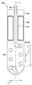
도 1a는 본 발명의 일부 구현예들에 따른, 모세관 툴의 사시도이다;
도 1b는 도 1a의 모세관 툴의 단면도이다;
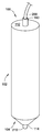
도 1c는 도 1a의 모세관 툴로서, 그 안에 위치된 본딩 와이어를 갖는 모세관 툴의 사시도이다;
도 1d는 본딩 와이어를 보다 양호하게 도시하기 위해 제거된 모세관 툴의 일 부분을 가진, 도 1c의 모세관 툴 및 본딩 와이어의 부분 사시도이다;
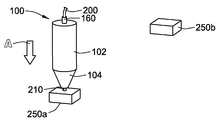
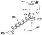
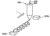
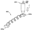
도 2a는 본 발명의 일부 구현예들에 따른, 한 쌍의 본드 패드들 중 제 1 본드 패드에 인접하여 위치된 도 1c의 모세관 툴 및 본딩 와이어의 사시도이다;
도 2b는 한 쌍의 본드 패드들 중 제 2 본드 패드를 향해 이동하는 도 2a의 모세관 툴 및 상기 모세관 툴로부터 분배되고 일반적인 나선형 또는 코일형 형상을 가진 본딩 와이어의 일 부분을 도시한 사시도이다;
도 2c는 상기 제 2 본드 패드에 인접하여 위치된 도 2b의 모세관 툴 및 본딩 와이어의 사시도이다;
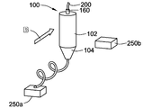
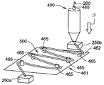
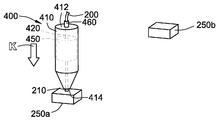
도 3a는 본 발명의 일부 구현예들에 따른, 한 쌍의 본드 패드들 중 제 1 본드 패드에 인접하여 위치된 모세관 툴 및 본딩 와이어의 사시도이다;
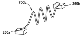
도 3b는 한 쌍의 본드 패드들 중 제 2 본드 패드를 향해 일반적인 구불구불한 경로로 고정구의 기둥들 주위에서 이동하는 도 3a의 모세관 툴 및 상기 모세관 툴로부터 분배된 본딩 와이어의 일 부분을 도시한 사시도이다;
도 3c는 상기 제 2 본드 패드에 인접하여 위치된 도 3b의 모세관 툴 및 본딩 와이어의 사시도이다;
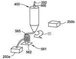
도 4a는 본 발명의 일부 구현예들에 따른, 한 쌍의 본드 패드들 중 제 1 본드 패드에 인접하여 위치된 모세관 툴 및 본딩 와이어의 사시도이다;
도 4b는 고정구의 단일 기둥 주위에 이동하는 도 4a의 모세관 툴 및 상기 모세관 툴로부터 분배되고 일반적인 코일형 형상을 가진 본딩 와이어의 일 부분을 도시한 사시도이다;
도 4c는 고정구가 제거되고, 도 4a의 모세관 툴이 한 쌍의 본드 패드들의 제 2 본드 패드를 향하여 이동되고, 일반적인 코일형 형상을 갖는 분배된 본딩 와이어가 신장되기 시작하는 사시도이다;
도 4d는 상기 제 2 본드 패드에 인접하여 위치되고 본딩 와이어의 일반적인 코일형 형상의 신장된 것을 도시한 모세관 툴의 사시도이다;
도 5a는 본 발명의 일부 구현예들에 따른, 한 쌍의 본드 패드들 중 제 1 본드 패드에 인접하여 위치된 모세관 툴 및 본딩 와이어의 사시도이다;
도 5b는 도 5a의 모세관 툴에 의해 일시적인 상호 연결부로 추적된 도 5a의 본딩 와이어 및 일시적인 상호 연결부를 구부리는 고정구의 사시도이다;
도 5c는 도 5b의 고정구에 의해 일반적인 구불구불한 형상을 가진 상호 연결부로 구부려진 도 5b의 일시적인 상호 연결부의 사시도이다;
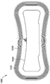
도 6은 본 발명의 일부 구현예들에 따른, 형성된 가요성 집적 회로의 사시도이다;
도 7은 본 발명의 일부 구현예들에 따른, 코일을 포함한 가요성 집적 회로의 평면도이다; 그리고
도 8은 본 발명의 일부 구현예들에 따른, 코일을 포함한 가요성 집적 회로의 평면도이다;
본 발명은 다양한 수정 및 대안적인 형태가 가능하지만, 특정 구현 예가 도면에서 예로서 도시되고 여기에 상세히 기술될 것이다. 그러나, 본 발명이 개시된 특정 형태에 한정되도록 의도되지 않는다는 것을 이해해야 한다. 오히려, 본 발명은 첨부된 청구 범위에 의해 정의된 바와 같이 본 발명의 기술 사상 및 권리 범위 내에 있는 모든 수정, 등가물 및 대안을 포괄하는 것이다.FIG. 1A is a perspective view of a capillary tool, in accordance with some embodiments of the present invention; FIG.
1B is a cross-sectional view of the capillary tool of FIG. 1A;
1C is a perspective view of a capillary tool of FIG. 1A having a bonding wire positioned therein; FIG.
1D is a partial perspective view of the capillary tool and bonding wire of FIG. 1C with a portion of the capillary tool removed to better illustrate the bonding wire;
2A is a perspective view of the capillary tool and bonding wire of FIG. 1C positioned adjacent to a first bond pad of a pair of bond pads, in accordance with some embodiments of the present invention;
FIG. 2B is a perspective view of the capillary tool of FIG. 2A moving toward the second bond pad of a pair of bond pads and a portion of a bonding wire having a common spiral or coil shape dispensed from the capillary tool; FIG.
Figure 2c is a perspective view of the capillary tool and bonding wire of Figure 2b positioned adjacent to the second bond pad;
3A is a perspective view of a capillary tool and bonding wire positioned adjacent a first bond pad of a pair of bond pads, in accordance with some embodiments of the present invention;
Figure 3b illustrates a portion of the capillary tool of Figure 3a and the bonding wire dispensed from the capillary tool, moving around pillars of the fixture in a generally serpentine path toward a second one of the pair of bond pads It is a perspective;
Figure 3c is a perspective view of the capillary tool and bonding wire of Figure 3b positioned adjacent to the second bond pad;
4A is a perspective view of a capillary tool and bonding wire positioned adjacent a first bond pad of a pair of bond pads, in accordance with some embodiments of the present invention;
Figure 4b is a perspective view of the capillary tool of Figure 4a moving around a single post of a fixture and a portion of a bonding wire having a general coil shape dispensed from the capillary tool;
Figure 4c is a perspective view in which the fixture is removed and the capillary tool of Figure 4a is moved toward the second bond pad of the pair of bond pads and the dispensed bonding wire having a general coil shape begins to elongate;
Figure 4d is a perspective view of a capillary tool positioned adjacent to the second bond pad and showing the elongation of the generally coiled shape of the bonding wire;
5A is a perspective view of a capillary tool and bonding wire positioned adjacent a first bond pad of a pair of bond pads, in accordance with some embodiments of the present invention;
Figure 5B is a perspective view of the bonding wire of Figure 5A tracked by the capillary tool of Figure 5A to a temporary interconnect and the fastener bending the temporary interconnect;
Fig. 5c is a perspective view of the temporary interconnections of Fig. 5b bent by the fasteners of Fig. 5b into interconnects having a common serpentine shape; Fig.
Figure 6 is a perspective view of a formed flexible integrated circuit, in accordance with some embodiments of the present invention;
Figure 7 is a plan view of a flexible integrated circuit including a coil, in accordance with some embodiments of the present invention; And
Figure 8 is a plan view of a flexible integrated circuit including a coil, in accordance with some embodiments of the present invention;
While the invention is susceptible to various modifications and alternative forms, specific embodiments are shown by way of example in the drawings and will herein be described in detail. It should be understood, however, that the invention is not intended to be limited to the particular forms disclosed. Rather, the invention is to cover all modifications, equivalents, and alternatives falling within the spirit and scope of the invention as defined by the appended claims.
이러한 개시 내용은 많은 다른 형태로 실시될 수 있지만, 본 발명이 본 발명의 원리의 예시로서 고려되어야 하고 본 발명의 넓은 양태를 제시된 구현예에 한정하는 것으로 의도되지 않음을 이해하는 것과 함께, 도면에 도시되어 있으며, 본 명세서에서 본 발명의 일부 예시적인 구현예들을 상세하게 기술할 것이다.While this disclosure is susceptible of embodiment in many different forms, it is to be understood that the invention is not to be considered as illustrative of the principles of the invention and is not intended to limit the broad scope of the invention to the embodiments shown, And some exemplary implementations of the invention will be described in detail herein.
도 1a 및 1b를 참조하여 보면, 한 쌍의 본드 패드들 사이에서 본딩 와이어를 공급, 굽힘 및 부착하는데 사용하기 위한 모세관 툴 (capillary tool) (100)은 몸체 (110), 가열 요소 (150) 및 옵션으로 초음파 변환기 (ultrasonic transducer) (160)를 포함한다. 모세관 툴 (100)의 몸체 (110)는 제 1 부분 (102) 및 제 2 부분 (104)을 포함한다. 몸체의 제 1 부분 (102)은 일반적으로 원통형 형상을 가지며, 그리고 제 2 부분 (104)은 일반적으로 원추형 형상을 가진다. 제 2 부분 (104)은 또한 모세관 툴 (100)의 팁으로도 지칭된다.1A and 1B, a
모세관 툴 (100)의 몸체 (110)는 모세관 툴 (100)의 제 1 표면 (112)으로부터 모세관 툴 (100)의 제 2 표면 (114)까지 연장되는, 모세관 또는 모세관 채널이라고도 지칭되는 내부 튜브 (120)를 가진다. 도시된 구현예에서, 제 1 표면 (112)은 상부 표면이고 제 2 표면 (114)은 하부 표면이지만, 내부 튜브 (120)는 모세관 툴 (100)의 다른 표면들 (예컨대, 측 표면 등)으로부터 시작 및/또는 종료될 수 있다. 내부 튜브 (120)는, 일반적인 직선형 또는 선형 형상을 가진 제 1 섹션 (122) 및 일반적인 나선형 또는 코일형 형상을 가진 제 2 섹션 (124)을 포함한다. 도시된 바와 같이, 내부 튜브 (120)의 제 1 섹션 (122)은 가열 요소 (150)를 통과하거나 그에 인접하지만, 마찬가지로 내부 튜브 (120)의 제 2 섹션 (124)의 일부 또는 모두는 가열 요소 (150)를 통과하거나 그에 인접 할 수 있다.The
내부 튜브 (120)의 제 2 섹션 (124)의 일반적인 나선형 형상은 오른손 잡이 또는 왼손잡이 일 수 있다. 도시된 바와 같이, 내부 튜브 (120)의 제 2 섹션 (124)의 일반적인 나선형 형상은 몸체 (110)의 중심 축 (Y) 둘레에서 약 2와 1/2 회의 완전한 회전을 포함하지만, 일반적인 나선형 형상의 임의의 횟수의 완전한 및/또는 부분적인 회전이 고려된다. 예를 들어, 내부 튜브 (120)의 제 2 섹션 (124)의 일반적인 나선형 형상은 몸체 (110)의 중심 축 (Y) 둘레에서 1/4 회의 완전한 회전을 가질 수 있다. 또 다른 예에 대해, 내부 튜브 (120)의 제 2 섹션 (124)의 일반적인 나선형 형상은 몸체 (110)의 중심 축 (Y) 둘레에서 1/2 회의 완전한 회전을 가질 수 있다. 또 다른 예에 대해, 내부 튜브 (120)의 제 2 섹션 (124)의 일반적인 나선형 형상은 몸체 (110)의 중심 축 (Y) 둘레에서 1 회의 완전한 회전을 가질 수 있다. 또 다른 예에 대해, 내부 튜브 (120)의 제 2 섹션 (124)의 일반적인 나선형 형상은 몸체 (110)의 중심 축 (Y) 둘레에서 2 회의 완전한 회전을 가질 수 있다. 또 다른 예에 대해, 내부 튜브 (120)의 제 2 섹션 (124)의 일반적인 나선형 형상은 몸체 (110)의 중심 축 (Y) 둘레에서 4 회의 완전한 회전을 가질 수 있다. 이로써, 중심 축 (Y) 둘레에서 임의의 횟수의 완전한 및/또는 부분적인 회전이 내부 튜브 (120)의 제 2 섹션 (124)에 포함될 수 있다는 것을 이해해야 한다.The general spiral shape of the
본 명세서에서 더 설명될 바와 같이, 내부 튜브 (120)의 제 2 섹션 (124)의 일반적인 나선형 형상은 모세관 툴 (100)로부터 분배된 본딩 와이어 (200)의 적어도 일 부분 (도 1c 및 1d)으로 하여금 내부 튜브 (120)의 제 2 섹션 (124)의 일반적인 나선형 형상의 기능인 일반적인 나선형 형상 (도 2b 및 도 2c에 도시됨)을 가지도록 한다. 일부 구현예에서, 본딩 와이어 (200)의 재료의 특성들 및/또는 가열 소자 (150)의 사양들 및/또는 다양한 다른 인자들/파라미터들, 이를테면 분배된 본딩 와이어 (200)의 원하는 특성들에 따라 모세관 툴 (100)을 설계할 때 회전 수가 변경된다.As described further herein, the general spiral shape of the
도 1a 및 1b에 도시된 바와 같이, 내부 튜브 (120)의 제 2 섹션 (124)의 일반적인 나선형 형상은 일반적인 일정한 피치 (pitch, P)를 가지며, 여기서 피치는 중심 축 (Y)과 평행하게 측정된, 내부 튜브 (120)의 제 2 섹션 (124)의 일반적인 나선형 형상의 1 회의 완전한 회전 또는 선회의 폭이다. 그러나, 대안 구현예들 (미도시)에서, 내부 튜브 (120)의 제 2 섹션 (124)의 일반적인 나선형 형상은 가변 피치, 제 1 피치를 갖는 제 1 부분 및 제 2 피치를 갖는 제 2 부분 등을 가질 수 있다.1A and 1B, the general spiral shape of the
도시된 바와 같이, 가열 요소 (150)는 몸체 (110)의 제 1 부분 (102) 내에 완전히 위치되지만, 가열 요소 (150)는, 가열 요소 (150)의 일 부분이 제 1 부분 (102), 제 2 부분 (104)에, 몸체 (110) 외부에, 또는 이들의 임의의 조합에 있도록 위치될 수 있다. 가열 요소 (150)는 내부 튜브 (120)의 제 1 섹션 (122)의 적어도 일 부분을 따라 열 영향 구역 (heat affect zone, HAZ)을 제공한다. 가열 요소 (150)는 본딩 와이어가 내부 튜브 (120)의 HAZ를 통과함에 따라 본딩 와이어 (200)를 가열하는데 사용된다. 모세관 툴 (100)의 원하는 출력에 따라, 가열 요소 (150)의 온도 및 내부 튜브 (120)의 HAZ는 본딩 와이어 (200)가 모세관 툴 (100)을 통해 분배되는 동안, 이전 및/또는 이후에 증가 및/또는 감소될 수 있다. 일부 구현예들에서, 가열 요소 (150)는 본딩 와이어 (200)를 형성하는 재료 및/또는 재료들의 유리 전이 온도 (Tg)보다 높은 온도로 본딩 와이어 (200)를 가열하도록 구성된다.As shown, the
도시된 바와 같이, 옵션의 초음파 변환기 (160)는 몸체 (110)의 제 1 부분 (102)으로부터 부분적으로 돌출되지만, 초음파 변환기 (160)는 초음파 변환기 (160)의 일 부분이 제 1 부분 (102), 제 2 부분 (104)에, 몸체 (110)의 외부에, 또는 이들의 임의의 조합에 있도록 위치될 수 있다. 초음파 변환기 (160)는 모세관 툴 (100)의 임의의 부분, 모세관 툴 (100)에 의해 맞닿는 본드 패드, 본딩 와이어 (200), 또는 이들의 임의의 조합에 전송될 수 있는 초음파 에너지를 제공하여, 예를 들어 본 명세서에 기술된 바와 같이 본드 패드에 본딩 와이어 (200)를 부착시키는데 도움을 준다. 도시된 초음파 변환기 (160)가 일반적인 원통형 튜브형 형상을 가지지만, 초음파 변환기 (160)는 예를 들어 큐브형 형상, 직사각형 형상 등과 같은 임의의 형상일 수 있다.As shown, the
도 1c 및 1d에 도시된 바와 같이, 본딩 와이어 (200)는 초음파 변환기 (160)를 통해 그리고 모세관 툴 (100)의 내부 튜브 (120) 내에 위치하고, 모세관 툴 (100)을 통해 소스 (예컨대, 본딩 와이어의 스풀(spool))로부터 분배될 준비를 한다. 한 쌍의 본드 패드들 사이에 본딩 와이어를 부착하기 시작하여 상호 연결을 생성하기 위해, 본딩 와이어 (200)의 일 부분이 모세관 디바이스 (100)의 팁 (104)으로부터 분배된다. 일부 구현예들에 따라서, 가열 요소 (150)는, 프리 에어 볼 (free air ball) (210)이 모세관 툴 (100)의 팁 (104)에 인접하게 형성되도록 본딩 와이어 (200)를 가열한다. 대안 구현예들에서, 열 및/또는 에너지의 별도의 소스 (미도시)는 프리 에어 볼 (210)로 하여금 형성하도록 사용된다.1C and 1D the
프리 에어 볼 (210)이 형성된 이후에, 상호 연결은 형성되어 한 쌍의 본드 패드들 사이에 부착될 준비를 한다. 모세관 툴 (100) (도 1a-1d)을 사용하여 상호 연결을 생성하기 위해, 한 쌍의 본드 패드들 사이에 본드 와이어를 부착하는 그러한 방법은 도 2a-2c를 참조하여 도시 및 기술된다. 도 2a를 참조하여 보면, 도 1c 및 도 1d의 모세관 툴 (100) 및 본딩 와이어 (200)는 한 쌍의 본드 패드들 (250a, 250b)에 대해 도시된다. 구체적으로, 모세관 툴 (100)은 프리 에어 볼 (210)이 제 1 본드 패드 (250a) 및 팁 (104)의 적어도 일 부분과 접촉하도록 위치된다. 본딩 와이어 (200)를 제 1 본드 패드 (250a)에 부착하기 위해, 열, 압력, 및/또는 초음파 에너지가 사용될 수 있다. 특히, 열은 적어도 부분적으로 가열 요소 (150)로부터 유도되고; 압력은 적어도 부분적으로 모세관 툴의 팁 (104)을 화살표 A 방향으로 하향 이동/가압함으로써 유도되며; 그리고 초음파 에너지는 적어도 부분적으로 초음파 변환기 (160)에 의해 유도된다. 일부 구현예들에 따라서, 열, 압력 및/또는 초음파 에너지의 조합은 프리 에어 볼 (210), 나아가 본딩 와이어 (200)를 제 1 본드 패드 (250a)에 부착시킨다. 그러한 프로세스는 열초음파 용접 (thermosonic welding)로 지칭될 수 있다. 본딩 와이어 (200)를 제 1 본드 패드 (250a)에 부착하는 다양한 다른 방법들이 고려될 수 있으며, 그리고 본 개시 내용의 기술된 프로세스/방법들에서 구현될 수 있다. 예를 들어, 본딩 와이어 (200)를 제 1 본드 패드 (250a)에 부착하는 또 다른 방법은 열 및 압력의 사용을 포함하지만, 초음파 에너지의 사용을 포함하지 않는다.After the
제 1 본드 패드 (250a)에 본딩 와이어 (200)가 부착되면 (도 2a), 모세관 툴 (100)은 일반적으로 제 2 본드 패드 (250b)를 향하여 화살표 B의 방향으로 이동된다 (도 2b). 모세관 툴 (100)의 이동은 본딩 와이어 (200)로 하여금 모세관 툴 (100)의 내부 튜브 (120)를 통해 그리고 모세관 툴 (100)의 제 2 표면 (114)에서 팁 (104) 밖으로 분배되도록 한다. 전술한 바와 같이, 내부 튜브 (120)의 제 2 섹션 (124)의 일반적인 나선형 형상은, 본딩 와이어 (200)로 하여금 내부 튜브 (120)의 제 2 섹션 (124)의 일반적인 나선형 형상 및 다른 파라미터들/인자들의 기능인 일반적인 나선형 형상으로 분배되도록 한다. 화살표 (B)의 방향으로의 모세관 툴 (100)의 이동 방향이 정확하게 수평일 필요가 없거나, 수평이 되지 않아도 됨을 유의한다. 오히려, 모세관 툴 (100)이 일부 방식으로 제 1 본드 패드 (250a)로부터 제 2 본드 패드 (250b)로 이동하는 한, 모세관 툴 (100)은 제 1 본드 패드 (250a)로부터 제 2 본드 패드 (250b)로 원호형 경로 (arc-like path)/트레이스를 취하거나 임의의 다른 경로/트레이스를 취할 수 있다. 일부 구현예들에서, 모세관 툴 (100)에 의해 취해진/추적된 경로는 본딩 와이어 (200)를 분배하는 것에 도움을 준다.When the
구체적으로, 본딩 와이어 (200)의 분배된 부분의 형상 및/또는 크기는, 예를 들어 일반적인 나선형 형상을 가진 내부 튜브 (120)의 제 2 섹션 (124)의 크기 및 형상, 본딩 와이어 (200) (예컨대, 금 와이어, 구리 와이어, 다른 금속 와이어 또는 이들의 임의의 조합)에 사용되는 와이어의 유형, 본딩 와이어 (200)의 크기/직경, 본딩 와이어 (200)의 영률과 같은 기계적 및/또는 물리적 속성들, 열 영향 구역 (HAZ) 내의 온도, HAZ의 길이, 모세관 툴 (100)에 의해 본드 패드들 사이에 이동된 경로, 모세관 툴 (100)이 본드 패드들 간에 이동하는 속도 등 또는 이들의 임의의 조합과 같은 다양한 파라미터들의 함수이다.In particular, the shape and / or size of the dispensed portion of the
일반적인 나선형 형상을 가진 내부 튜브 (120)의 제 2 섹션 (124)의 크기 및 형상은 회전 직경 D, 다수의 완전한 및/또는 부분적인 회전 N, 및 총 회전 길이 L를 포함하는 기하학적 변수들에 대해 정의될 수 있다. 본 개시 내용의 일부 구현예들에서, 회전 직경 D는 약 100 마이크로미터, 약 500 마이크로미터, 약 1 밀리미터 등일 수 있다. 본 개시 내용의 일부 구현예들에서, 회전 직경 D는 약 50 마이크로미터 내지 약 2 밀리미터일 수 있다. 본 개시 내용의 일부 구현예들에서, 완전한 및/또는 부분적인 회전 수 N은 약 2 회, 약 5 회, 약 10 회, 약 50 회 등일 수 있다. 본 개시 내용의 일부 구현예들에서, 완전한 및/또는 부분적인 회전 수 N은 약 0.5 내지 약 200 회일 수 있다. 본 개시 내용의 일부 구현예들에서, 총 회전 길이 L은 약 500 마이크로미터, 약 1 밀리미터, 약 5 밀리미터, 약 1 센티미터 등일 수 있다. 본 개시 내용의 일부 구현예들에서, 총 회전 길이 L은 약 200 마이크로미터 내지 약 3 센티미터일 수 있다.The size and shape of the
도 1b를 다시 참조하여 보면, 모세관 툴 (100)에 대한 기하학적 파라미터들 D, N 및 L이 도시되어 있으며, 여기서 N은 약 2.5이다. 기하학적 파라미터들을 정의 및 측정하는 다양한 다른 방법들이 고려된다. 모세관 툴 (100)에 대한 기하학적 파라미터들 D, N 및 L이 본딩 와이어 (200)의 분배된 부분의 유사한 기하학적 파라미터들과 일대일 방식으로 반드시 대응될 필요가 없음을 유의한다. 즉, 일부 구현예들에서, 일반적인 나선형 형상을 가진 내부 튜브 (120)의 제 2 섹션 (124)의 회전 직경 D는 일반적인 나선형 형상을 가진 분배된 본딩 와이어 (200)의 직경과 같거나, 그 직경보다 크거나 또는 작을 수 있다 (도 2c 참조). 유사하게, 예를 들어, 일부 구현예들에서, 일반적인 나선형 형상을 가진 내부 튜브 (120)의 제 2 섹션 (124)의 회전 수 (N)는 일반적인 나선형 형상을 가진, 분배된 본딩 와이어 (200)의 회전 수와 같거나, 그보다 크거나 그보다 작을 수 있다 (도 2c 참조). 이로써, 본딩 와이어 (200)의 분배된 부분의 일반적인 나선형 형상은 내부 튜브 (120)의 제 2 섹션 (124)의 일반적인 나선형 형상과는 서로 다를 수 있다.Referring again to FIG. 1B, the geometric parameters D, N, and L for the
모세관 툴 (100)이 제 2 본드 패드 (250b)에 접근할 때까지, 모세관 툴 (100)은 화살표 B의 방향으로 계속 이동한다 (도 2b). 도 2c에 도시된 바와 같이, 모세관 툴 (100)은 일반적으로 화살표 C 방향으로 이동하여 본딩 와이어 (200)의 일 부분이 제 2 본드 패드 (250b)와 접촉하도록 위치시킨다. 그 후에, 모세관 툴 (100)은 열, 압력 및/또는 초음파 에너지를, 제 2 본드 패드 (250b)와 접촉하는 본딩 와이어 (200)의 일 부분에 가하여, 프리 에어 볼 (210)이 제 1 본드 패드 (250a)에 접촉하는 법과 유사한 방식으로, 본딩 와이어 (200)를 제 2 본드 패드 (250b)에 부착하는데 사용된다.The
본딩 와이어 (200)가 제 1 및 제 2 본드 패드들 (250a, 250b)에 부착 된 상태에서, 모세관 툴 (100)은 본딩 와이어 (200)로 하여금 제 2 본딩 패드 (250b) 근방에서 스플리팅 (splitting), 스냅핑 (snapping) 또는 브레이킹 (breaking)하도록 하고, 그 결과 본딩 와이어 (200)는 제 2 본드 패드 (250b)에 부착된 상태를 유지하며, 그리고 모세관 툴 (100)은 서로 다른 쌍의 본드 패드들 사이에서 본딩 와이어 (200)를 부착하기 하기 위해 이동될 수 있다 (미도시). 제 1 본드 패드 (250a)와 제 2 본드 패드 (250b) 사이에 부착되는 본딩 와이어 (200)의 분배된 부분은 상호 연결부 (300)로 지칭된다.With the
도 2c에 도시된 바와 같이, 상호 연결부 (300)는 제 1 본드 패드 (250a)와 제 2 본드 패드 (250b)를 연결시킨다. 상호 연결부 (300)가 적어도 부분적으로 전기 전도성 재료로 형성되기 때문에, 상호 연결부 (300)는 제 1 본드 패드 (250a)를 제 2 본드 패드 (250b)에 전기적으로 결합시킨다. 본드 패드들 (250a, 250b)은 집적 회로 (IC)의 임의의 유형 및 / 또는 임의의 부분과 전기적으로 결합되거나 일체형될 수 있다. 도시된 바와 같이, 상호 연결부 (300)는 가요성 및 굴곡성인 일반적인 나선형 형상을 가진다. 상호 연결부 (300)의 일반적인 나선형 형상은, 본드 패드들 (250a, 250b) (및 각각이 부착된 전자 기기들)이 본드 패드들 (250a, 250b) 중 어느 하나로의 상호 연결부 (300)의 부착을 파손시킴 없이, 서로에 대해 3 차원 공간 (예컨대, X 방향, Y 방향 및/또는 Z 방향)으로 이동되는 것을 허용한다. 즉, 예를 들어, 상호 연결부 (300)는 그의 X 축을 따라 신장되고 길게 늘어질 수 있다. 더욱이, 예를 들어, 상호 연결부 (300)는 그의 X 축을 따라 압축 및 수축할 수 있다. 여전히 더욱이, 예를 들어, 상호 연결부 (300)는 그의 Y 축 및 Z 축에 대해 구부러지고 휘어질 수 있다.As shown in FIG. 2C, the
상기에서 논의한 바와 같이, 상호 연결부 (300)의 완전한 회전 수는 모세관 툴 (100)에 의해 본드 패드들 (250a, 250b) 사이를 이동하는 경로를 포함하여 상기에서 논의된 파라미터들의 함수이다. 상호 연결부 (300)의 회전 수 또는 코일 수는 본드 패드들 (250a, 250b) 사이의 거리가 증가함에 따라 증가할 것이다. 이로써, 일부 구현예들에서, 상기의 파라미터들에 따라, 상호 연결부 (300)는 2 개 이상의 완전한 회전 또는 컬 (curls)을 가질 것이다. 도 2c에 도시된 바와 같은 일부 다른 구현예들에서, 상호 연결부 (300)는 약 6 회의 완전한 회전 또는 컬을 가질 것이다. 일부 다른 구현예들에서, 상호 연결부 (300)는 10 회 이상의 완전한 회전 또는 컬을 가질 것이다. 여전히 일부 다른 구현예들에서, 상호 연결부 (300)는 30 회 이상의 완전한 회전 또는 컬을 가질 것이다.As discussed above, the complete number of turns of the
상기의 구현예들이 예를 들어, 나선형 형상과 같은 일반적인 비-선형 형상을 갖는 내부 튜브 (120)의 제 2 섹션 (124)을 가진 모세관 툴 (100)의 사용을 포함하지만, 그러한 모세관 툴 (100)을 사용하는 대신에, 그러한 일반적인 나선형 형상 내부 튜브가 없는 모세관 툴 (400)은 한 쌍의 본드 패드들 사이에 가요성 및 굴곡성 상호 연결을 생성하기 위해 고정구 (fixture) (예컨대, 고정구 (461, 561))와 조합하여 사용될 수 있다.Although the above embodiments include the use of a
도 3a 내지 도 3c를 참조하면, 모세관 툴 (400)은 한 쌍의 본드 패드들 (250a, 250b) 사이에서 본딩 와이어 (200)를 공급, 굽힘 및 부착하는데 사용하기 위해 도시되며, 여기서 동일한 참조 번호는 본 명세서에 기술된 유사한 구성요소들에 사용된다. 모세관 툴 (400)은, 모세관 툴 (400)이 몸체 (110), 가열 요소 (150), 및 초음파 변환기 (160)와 동일하거나 유사한 몸체 (410), 가열 요소 (450) 및 옵션으로 초음파 변환기 (460)를 포함한다는 점에서 모세관 툴 (100)과 유사하다. 그러나, 모세관 툴 (400)은 또한 모세관 툴 (100)의 내부 튜브 (120)와 같이 일반적인 나선형 형상을 갖는 제 2 섹션을 포함하지 않는 내부 튜브 (420)를 포함한다. 오히려, 모세관 툴 (400)은 선형 (410)의 제 1 표면 (412)으로부터 몸체 (410)의 제 2 표면 (414)까지 일반적인 직선형 또는 선형을 가진 내부 튜브 (420)를 포함한다.3A-3C, a
도 3a 내지 도 3c에 도시된 본딩 패드들 (250a, 250b) 사이에 가요성 및 굴곡성 상호 연결을 제공하기 위하여, 모세관 툴 (400)은 모세관 툴 (100)과 관련하여 전술한 방식과 동일하거나 유사한 방식으로 본딩 와이어 (200)를 제 1 본드 패드 (250a)에 부착하는데 사용된다. 구체적으로, 프리 에어 볼 (210)은, 모세관 툴 (400)이 열, 압력 및 초음파 에너지를 가하는 화살표 D의 방향으로 이동함에 따라, 제 1 본드 패드 (250a)에 형성 부착된다.The
제 1 본드 패드 (250a)에 본딩 와이어 (200)가 부착된 상태에서 (도 3a), 모세관 툴 (400)은 일반적인 구불구불한 경로 (serpentine path)와 같은 일반적인 비-선형 경로로 고정구 (461)의 다수의 기둥들 (posts) (465) 주위에 이동된다 (예컨대, 도 3b의 화살표 E). 고정구 (461)의 기둥들 (465)은 기둥들 (465)이 서로에 대해 고정 및 공지된 위치에 위치되도록 공통 베이스 플레이트 (462)에 부착된다. 더욱이, 고정구 (461)는 한 쌍의 본드 패드들 (250a, 250b) 및 모세관 툴 (400)에 대해 공지된 상대적인 배향 및 위치로 위치된다. 그와 같이, 일부 구현예들에 따르면, 모세관 툴 (400)은 반복 가능한 상호 연결을 제공하기 위해 기둥들 (465) 주위에 미리 프로그래밍된 구불구불 한 경로를 따라 이동할 수 있다.3A), the
일반적인 구불구불 한 경로에서 모세관 툴 (400)의 이동은 본딩 와이어 (200)로 하여금 모세관 툴 (400)의 내부 튜브 (420)를 통해 그리고 모세관 툴 (400)의 제 2 표면 (414)에서의 팁 밖으로 분배되도록 한다. 모세관 툴 (400)이 기둥들 (465) 주위에서 이동함에 따라, 본딩 와이어 (200)는 기둥들 (465)과 맞물려 그 주위에서 구부러지고/변형된다. 가열 요소 (450)는, 본딩 와이어 (200)가 기둥들 (465) 주위로 분배될 시에, 분배된 본딩 와이어 (200)의 온도가 그 주위의 본딩 와이어 (200)의 굽힘 및/또는 변형에 도움을 주도록, 본딩 와이어 (200)를 가열하는데 사용될 수 있다.The movement of the
모세관 툴 (400)이 제 2 본드 패드 (250b)에 접근할 때까지 모세관 툴 (400)은 일반적인 구불구불한 경로로 계속 이동한다 (도 3b). 도 3c에 도시된 바와 같이, 모세관 툴 (400)은 그 후에 일반적으로 화살표 F의 방향으로 이동되어 본딩 와이어 (200)의 일 부분이 제 2 본드 패드 (250b)와 접촉하도록 위치시킨다. 그 후에, 모세관 툴 (400)은 열, 압력 및/또는 초음파 에너지를, 제 2 본드 패드 (250b)와 접촉하는 본딩 와이어 (200)의 일 부분에 가하여, 본딩 와이어 (200)를 제 2 본드 패드 (250b)에 부착하는데 사용된다.The
본딩 와이어 (200)가 제 1 및 제 2 본드 패드들 (250a, 250b)에 부착 된 상태에서, 모세관 툴 (400)은 도 2c와 관련하여 전술된 것과 유사하게, 본딩 와이어 (200)로 하여금 제 2 본딩 패드 (250b) 근방에서 스플리팅, 스냅핑 또는 브레이킹하도록 할 수 있다. 그러한 바와 같이, 모세관 툴 (400)은 고정구 (461) 또는 유사한 고정구를 반복적인 방식으로 사용하여, 서로 다른 쌍의 본드 패드들 (미도시) 사이에 본딩 와이어 (200)를 부착하도록 자유롭게 이동한다. 즉, 본딩 와이어 (200)가 제 2 본드 패드 (250b)에 부착된 이후에, 고정구가 제거되어, 본딩 와이어 (200)가 기둥들 (465)로부터 결합 해제될 수 있다. 고정구가 결합 해제되면, 본딩 와이어 (200)는 부분적으로 소정의 기억 정도를 가진 본딩 와이어 (200)로 인해, 그의 일반적인 구불구불한 형상을 유지한다. 도 3c에 도시된 바와 같이, 제 1 본드 패드 (250a)와 제 2 본드 패드 (250b) 사이에 부착되는 본딩 와이어 (200)의 분배된 부분은 상호 연결부 (500)로 지칭된다.With the
이제, 도 4a 내지 도 4d를 참조하면, 모세관 툴 (400)은 고정구 (561)를 사용하여 한 쌍의 본드 패드들 (250a, 250b) 사이에서 본딩 와이어 (200)을 공급, 굽힘 및 부착하는데 사용하기 위해 도시되며, 여기서 동일한 참조 번호는 본 명세서에 기술된 유사한 구성요소들에 사용된다. 모세관 툴 (400)은 도 3a-3c와 관련하여 기술된 바와 같은 유사한 방식으로 사용되지만, 그러나, 모세관 툴 (400)을 일반적인 구불구불한 경로로 이동시키는 대신에, 모세관 툴 (400)은 본딩 와이어 (200)의 하나 이상의 코일들을 그 주위에서 생성하기 위해, 고정구 (561)의 베이스 플레이트 (562)에 부착된 단일 기둥 (565) 주위에서 적어도 1 번 이동된다.4A-4D, a
구체적으로, 도 4a를 참조하여 보면, 모세관 툴 (400)이 열, 압력 및/또는 초음파 에너지를 가하는 화살표 G의 방향으로 이동함에 따라, 프리 에어 볼은 제 1 본드 패드 (250a)에 형성 및 부착된다.4a, as the
본딩 와이어 (200)가 제 1 본드 패드 (250a)에 부착된 상태에서 (도 4a), 모세관 툴 (400)은 본딩 와이어 (200)의 하나 이상의 코일들을 기둥 (565) 주위에서 생성하기 위해, 고정구 (561)의 기둥 (565) 주위에서 화살표 H 방향으로 적어도 1 번 이동된다 (도 4b). 고정구 (561)는 한 쌍의 본드 패드들 (250a, 250b) 및 모세관 툴 (400)에 대해 공지된 상대적인 배향 및 위치로 위치된다. 그와 같이, 일부 구현예들에 따르면, 모세관 툴 (400)은 일반적인 반복 가능한 상호 연결을 제공하기 위해 기둥 (465) 주위에 미리 프로그래밍된 경로를 따라 이동할 수 있다.4A), the
기둥 (565) 주위에서 모세관 툴 (400)의 이동은 본딩 와이어 (200)로 하여금 모세관 툴 (400)의 내부 튜브 (420)를 통해 그리고 모세관 툴 (400)의 제 2 표면 (414)에서의 팁 밖으로 분배되도록 한다. 모세관 툴 (400)이 기둥 (565) 주위에서 이동함에 따라, 본딩 와이어 (200)는 기둥들 (565)과 맞물려 그 주위에서 구부러지고/변형된다. 모세관 툴 (400)의 가열 요소 (450)는, 본딩 와이어 (200)가 기둥들 (465) 주위로 분배될 시에, 분배된 본딩 와이어 (200)의 온도가 그 주위의 본딩 와이어 (200)의 굽힘 및/또는 변형에 도움을 주도록, 본딩 와이어 (200)를 가열하는데 사용될 수 있다.The movement of the
본딩 와이어 (200)의 원하는 코일 수가 만들어질 때까지 모세관 툴 (400)은 화살표 H의 방향으로 일반적으로 기둥 (565) 주위에서 이동하도록 구성된다 (도 4b). 원하는 코일 수가 만들어진 이후에, 고정구 (561)가 제거되어, 본딩 와이어 (200)는 기둥 (565)으로부터 결합 해제된다. 고정구 (561)가 결합 해제되면, 본딩 와이어 (200)는 부분적으로 소정의 기억 정도를 가진 본딩 와이어 (200)로 인해, 그의 일반적인 코일형 형상을 유지한다. 본 개시 내용의 일부 구현예들에서, 모세관 툴 (400)은, 본딩 와이어 (200)의 코일들 중 각각의 추가 코일이 이전 코일보다 약간 큰 직경으로 형성되도록 단일의 일반적인-수평 평면에서 화살표 (H)의 방향으로 기둥 (565) 주위를 이동하는 것이 고려된다. 대안적으로, 모세관 툴 (400)은 본딩 와이어 (200)의 코일들 중 각각의 추가 코일이 이전 코일 (들)과 거의 동일한 직경으로 형성되도록 다수의 일반적인-수평 평면들에서, 그리고 기둥 (565)을 따라 약간 다른 높이로, 화살표 (H)의 방향으로 기둥 (565) 주위에서 이동할 수 있다.The
고정구 (561)가 도중에 없어지면, 모세관 툴 (400)은 일반적으로 화살표 I의 방향으로 제 2 본드 패드 (250b)를 향해 이동된다. 모세관 툴이 화살표 I의 방향으로 이동함에 따라, 본딩 와이어 (200)의 코일들은 도 4d에 도시된 바와 같이 일반적인 코일형 또는 나선형 형상으로 신장 및 정렬되기 시작한다. 더욱이, 도 4d에 도시된 바와 같이, 모세관 툴 (400)은 그 후에 일반적으로 화살표 J의 방향으로 이동되어 본딩 와이어 (200)의 일 부분이 제 2 본드 패드 (250b)와 접촉하도록 위치시킨다. 모세관 툴 (400)은 그 후에 제 2 본드 패드 (250b)와 접촉하는 본딩 와이어 (200)의 일 부분에 열, 압력 및/또는 초음파 에너지를 가하여 본딩 와이어 (200)를 제 2 본드 패드 (250b)에 부착시키는데 사용된다.When the
본딩 와이어 (200)가 제 1 및 제 2 본드 패드들 (250a, 250b)에 부착 된 상태에서, 모세관 툴 (400)은 도 2c와 관련하여 전술된 것과 유사하게, 본딩 와이어 (200)로 하여금 제 2 본딩 패드 (250b) 근방에서 스플리팅, 스냅핑 또는 브레이킹하도록 할 수 있다. 그러한 바와 같이, 모세관 툴 (400)은 고정구 (561) 또는 유사한 고정구를 일반적인 반복 가능한 방식으로 사용하여, 서로 다른 쌍의 본드 패드들 (미도시) 사이에 본딩 와이어 (200)를 부착하도록 자유롭게 이동한다. 도 4d에 도시된 바와 같이, 제 1 본드 패드 (250a)와 제 2 본드 패드 (250b) 사이에 부착 된 본딩 와이어 (200)의 분배된 부분은 상호 연결부 (600)로 지칭된다.With the
이제, 도 5a-5c를 참조하여 보면, 고정구 (661)를 사용하여 한 쌍의 본드 패드들 (250a, 250b) 사이에 본딩 와이어 (200)를 공급 및 부착하는데 사용하기 위해 모세관 툴 (400)이 도시되고 (도 5b), 여기서 유사한 참조 번호는 본 명세서에 기술된 유사한 구성요소들에 대해 사용된다. 모세관 툴 (400)은 도 3a-3c와 관련하여 기술된 바와 같은 유사한 방식으로 사용되지만, 그러나, 고정구 (예를 들어, 고정구 (461, 561))의 기둥들 주위에 일반적인 구불 구불한 경로로 모세관 툴 (400)을 이동시키는 대신에, 모세관 툴 (400)은 제 1 본드 패드 (250a)로부터 제 2 본드 패드 (250b) 까지, 화살표 M의 방향으로, 일반적인 원호-형상의 경로로 이동되어 (도 5b), 길이 (Li) 및 최대 높이 (Hi-max)를 가진 임시 상호 연결부 (700a)를 그 사이에서 형성한다 (도 5b에 도시됨). "일시적인 (temporary)"은, 일시적인 상호 연결부 (700a)가 상호 연결부 (700b) (도 5c)를 형성하기 위해 서로 다른 형상을 가지도록 고정구 (661)에 의해 수정될 시에 (도 5c), 임시 상호 연결부 (700a)가 상호 연결부의 최종 형태로 고려되지 않는다는 것을 의미한다.5A-5C, a
구체적으로, 도 5a를 참조하여 보면, 모세관 툴 (400)이 열, 압력 및/또는 초음파 에너지를 가하는 화살표 K의 방향으로 이동함에 따라, 프리 에어 볼 (210)은 제 1 본드 패드 (250a)에 형성 및 부착된다. 제 1 본드 패드 (250a)에 본딩 와이어 (200)가 부착된 상태에서 (도 5a), 모세관 툴 (400)은 화살표 M의 방향으로 일반적으로 원호-형상의 경로로 이동되어 (도 5b), 길이 (Li) 및 최대 높이 (Hi-max)를 가진 일시적인 상호 연결부 (700a)를 생성한다. 본드 패드들 (250 a, b) 사이의 모세관 툴 (400)의 이동은 본딩 와이어 (200)로 하여금 모세관 툴 (400)의 내부 튜브 (420)를 통해 그리고 모세관 툴 (400)의 제 2 표면 (414)에서 팁 밖으로 분배되도록 한다. 더욱이, 도 5b에 도시된 바와 같이, 모세관 툴 (400)은 그 후에 일반적으로 화살표 N의 방향으로 이동되어 본딩 와이어 (200)의 일 부분이 제 2 본드 패드 (250b)와 접촉하도록 위치시킨다. 모세관 툴 (400)은 그 후에 제 2 본드 패드 (250b)와 접촉하는 본딩 와이어 (200)의 일 부분에 열, 압력 및/또는 초음파 에너지를 가하여 본딩 와이어 (200)를 제 2 본드 패드 (250b)에 부착시키는데 사용된다.5a, as the
본딩 와이어 (200)가 제 1 및 제 2 본드 패드들 (250a, 250b)에 부착 된 상태에서, 모세관 툴 (400)은 도 2c와 관련하여 전술된 것과 유사하게, 본딩 와이어 (200)로 하여금 제 2 본딩 패드 (250b) 근방에서 스플리팅, 스냅핑 또는 브레이킹하도록 할 수 있다. 그러한 바와 같이, 모세관 툴 (400)은 고정구 (661) 또는 유사한 고정구를 일반적인 반복 가능한 방식으로 사용하여, 서로 다른 쌍의 본드 패드들 (미도시) 사이에 본딩 와이어 (200)를 부착하도록 자유롭게 이동한다.With the
본딩 와이어 (200)가 스플리팅, 스냅핑 또는 브레이킹되도록 야기된 후에, 또는 그러한 액션 이전에, 고정구 (661)는 본딩 와이어 (200)를 도 5c에 도시된 바와 같이 일반적인 구불구불한 형상 또는 일반적인 지그재그 형상으로 구부리는데 사용된다. 구체적으로, 도 5b에 도시된 바와 같이, 고정구 (661)는 제 1 굽힘 부재 (661a)와 제 2 굽힘 부재 (661b)를 포함한다. 제 1 굽힘 부재 (661a)는 베이스 (662a)에 결합된 복수의 기둥들 또는 핑거들 (665a)을 포함한다. 유사하게, 제 2 굽힘 부재 (661b)는 베이스 (662b)에 결합된 복수의 기둥들 또는 핑거들 (665b)을 포함한다.After the
본드 와이어 (200)가 일반적인 구불구불한 형상을 가지도록 (도 5c에 도시됨), 본드 패드들 (250a, b) 사이에서 추적되는 본드 와이어 (200)를 변형하기 위해 (도 5a), 제 1 및 제 2 굽힘 부재들 (661a, b)은 화살표들 (O 및 Q) 각각의 방향으로 서로를 향해 이동된다. 구체적으로, 제 1 및 제 2 굽힘 부재들 (661a, 662b)는 핑거들 (665a, 665b)이 도 5b에 최적으로 도시된 바와 같이 번갈아 생기도록 서로로부터 오프셋된다. 이로써, 제 1 및 제 2 굽힘 부재들 (661a, 662b)이 서로 끼워짐에 따라, 본딩 와이어 (200)는 핑거들 (665a, 665b) 사이에 가압되며, 그리고 도 5c에 도시된 일반적인 구불구불한 형상으로 굽혀지고, 그리고/또는 가압된다.To deform the
굽힘 부재들 (661a, b) 각각이 3 개의 핑거들 (665a, b)을 포함하는 것으로 도시되었지만, 굽힘 부재들 (661a, b) 각각은 임의의 수의 핑거들 (665a, b)을 포함할 수 있다. 예를 들어, 각각의 굽힘 부재 (661a, b)는 2 개의 핑거들, 4 개의 핑거들, 5 개의 핑거들, 10 개의 핑거들 등을 포함할 수 있다. 추가적으로, 핑거들 (665a, b) 각각 사이의 거리는, 예를 들어, 상호 접속부 (700b)의 형성된 구불구불한 형상의 피치를 제어하기 위해 변형될 수 있다. 각각의 핑거 (665a, b) 사이의 간격은 예를 들어, 핑거들 (665a, b)과 베이스 (662a, b) 사이의 슬라이딩 메커니즘과 같은 메커니즘 (미도시)을 사용하여 조정될 수 있다. 구체적으로, 예를 들어, 핑거들 각각은 베이스 (662a, b) (예컨대, 베이스의 길이 방향 축을 따라)와 슬라이딩 가능하게 맞닿을 수 있고, (예컨대, 고정 스크류 등을 사용하여) 제 위치에 잠길 수 있다. 이러한 대안적인 구현예들에서, 핑거들은 텅-앤-그루브 방식 (tongue-and-groove fashion)으로, 또는 임의의 다른 기계적 메커니즘을 사용하여, 베이스에 슬라이딩 가능하게 맞닿을 수 있다. 핑거들 (665a, b) 사이의 그러한 간격 조정은 굽힘 부재들 (661a, b)이 함께 끼어 있기 전, 중 및/또는 후에 발생될 수 있는 것으로 고려된다. 즉, 일부 구현예들에서, 핑거들 (665a, b) 사이의 간격이 설정되고 그 후에 굽힘 부재들 (661a, b)이 서로 끼여진다. 일부 다른 구현예들에서, 핑거들 (665a, b)은 그 사이에 제 1 간격을 가지며, 그 후에 굽힘 부재들 (661a, b)가 함께 끼여지고, 그 이후에 핑거들 (665a, b)이 제 1 간격과는 다른 제 2 간격을 가지도록 이동/조정되고, 그 이후에 굽힘 부재들 (661a, b)이 풀어지고/분리된다. 다양한 상호 연결부 형상들을 형성하기 위해 핑거들 (665a, b) 사이의 간격을 조정하고 끼우고/푸는 다양한 다른 방법들/계획들이 고려된다.Although each of the
도시된 바와 같이, 상호 연결부 (700b) (도 5c)는 일반적으로 X-Z 평면 내에 있다; 그러나, 상호 연결부 (700)는 임의의 평면에 추적될 수 있다 (예컨대, 제 1 본드 패드와 제 2 본드 패드 (250a, b) 사이에 연결됨). 예를 들어, 일부 구현예들에서, 상호 연결부 (700b)는 X-Y 평면에 위치될 수 있다. 그러한 대안에서, 고정구 (661)의 위치 설정은 대응하는 서로 다른 평면에서 이동하여 그에 따라 본딩 와이어 (200)를 포착 및 구부리도록 변형된다.As shown,
본 명세서 전체에 걸쳐 기술된 본딩 와이어 (200)는 하나 이상의 전기 전도성 재료들을 포함할 수 있다. 일부 구현예들에서, 본딩 와이어 (200)는 예를 들어 알루미늄, 스테인리스 강, 전이 금속, 탄소, 구리, 은, 금, 백금, 아연, 니켈, 티타늄, 크롬 또는 팔라듐을 갖는 합금들을 포함한 금속 합금, 인듐 주석 산화물 또는 다른 투명 전도성 산화물, 또는 III-IV 족 전도체들 (GaAs 포함)을 포함한 실리콘계 전도성 재료를 포함한 반도체계 전도성 재료, 또는 이들의 임의의 조합과 같은 전기 전도성 재료들을 포함한다.The
일부 다른 구현예들에서, 전기 전도성 재료들은 하나 이상의 전기 절연 재료들, 이를테면, 예를 들어 폴리머 또는 폴리머 재료, 이를테면, 폴리이미드, 폴리에틸렌 테레프탈레이트 (PET), 실리콘 또는 폴리 우레탄, 플라스틱, 엘라스토머, 열가소성 엘라스토머, 엘라스토플라스틱 (elastoplastics), 서모 스탯 (thermostats), 열가소성 수지, 아크릴레이트, 아세탈 폴리머, 생분해성 폴리머, 셀룰로오스 폴리머, 플루오로폴리머, 나일론, 폴리아크릴로니트릴 폴리머, 폴리아미드-이미드 폴리머, 폴리아릴레이트, 폴리벤즈이미다졸, 폴리부틸렌, 폴리카보네이트, 폴리에스테르, 폴리에테르이미드, 폴리에틸렌, 폴리에틸렌 코폴리머 및 개질된 폴리에틸렌, 폴리케톤, 폴리메틸메타 크릴레이트, 폴리메틸펜텐, 폴리페닐렌 옥사이드 및 폴리페닐렌 설파이드, 폴리프탈 아미드, 폴리프로필렌, 폴리우레탄, 스티렌계 수지, 술폰계 수지, 비닐계 수지, 또는 이들의 임의의 조합물로 코팅된다.In some alternative embodiments, the electrically conductive materials may comprise one or more electrically insulating materials such as, for example, polymer or polymeric materials such as polyimide, polyethylene terephthalate (PET), silicone or polyurethane, plastic, elastomer, thermoplastic But are not limited to, elastomers, elastomers, thermostats, thermoplastics, acrylates, acetal polymers, biodegradable polymers, cellulosic polymers, fluoropolymers, nylons, polyacrylonitrile polymers, But are not limited to, polyarylates, polybenzimidazoles, polybutylenes, polycarbonates, polyesters, polyetherimides, polyethylenes, polyethylene copolymers and modified polyethylenes, polyketones, polymethylmethacrylates, polymethylpentenes, polyphenylene oxides And polyphenylene sulfide, polyphthalamide Polyurethane, polypropylene, polyurethane, styrenic resin, sulfonic resin, vinylic resin, or any combination thereof.
일부 구현예들에서, 본 발명의 모세관 툴들 (100, 400) 및/또는 본 발명의 고정구들 (461, 561, 661) 중 하나 이상 및/또는 별도의 디바이스는, 상호 연결부를 고형화하는데 도움을 주고 그리고/또는 상호 연결부의 형상을 유지하는데 도움을 주기 위해 (예컨대, 일반적인 구불구불한 형상, 일반적인 나선형 등), 상호 연결부 (300, 500, 600, 700b 등) (예컨대, 전기 전도성 재료로 만들어진 본딩 와이어 (200)로 형성됨)를 캡슐화하는 소정의 재료 (예컨대, 본 명세서에 기술된 전기 절연 재료들 중 하나 이상)를 분배하는 분배 구성요소를 포함한다. 일부 구현예들에서, 분배된 캡슐화 재료는 전기적으로 절연될 수 있고, 실리콘, 폴리우레탄 및/또는 저밀도 폴리에스테르와 같은 폴리머일 수 있다. 일부 구현예들에서, 분배된 캡슐화 재료의 영률은 최대 약 0.1 Kpa, 최대 약 10 Kpa, 최대 약 0.1 Mpa, 최대 약 10 Mpa 등의 범위일 수 있다.In some embodiments, the
일부 구현예들에서, 전기 절연 재료들은 본딩 와이어 (200)를 예를 들어 3.3 볼트, 6.7 볼트 등과 같은 공급 전압까지 전기적으로 절연시킨다.In some embodiments, the electrically insulating materials electrically isolate the
본 명세서에 기술되고 본딩 와이어 (200)로 형성된 상호 연결부 (300, 500, 600)는 상술된 전기 전도성 재료들 및/또는 전기 절연성 재료들로 제조될 수 있다. 일부 구현예들에 따라, 상호 연결부들 (300, 500, 600)을 형성하는데 사용된 재료들과 관계없이, 각각의 상호 연결부 (300, 500, 600)는 예를 들어 약 0.1 ㎛, 약 0.3 ㎛, 약 0.5 ㎛, 약 0.8 ㎛, 약 1 ㎛, 약 1.5 ㎛, 약 2 ㎛, 약 5 ㎛, 약 9 ㎛, 약 12 ㎛, 약 25 ㎛, 약 50 ㎛, 약 75 ㎛, 약 100 ㎛를 포함하여, 약 0.1㎛ 내지 약 100㎛의 두께 또는 임의의 다른 두께를 가질 수 있다.
본원에 기술된 바와 같이, 가열 요소 (150, 450)는 본딩 와이어 (200)를 가열하기 위해 사용된다. 일부 구현예들에 따라서, 본딩 와이어 (200)의 가열은 그의 유리 전이 온도 (Tg)를 초과하여 가열할 시에, 본딩 와이어 (200)를 용융된 유리형 상태로 변형시킨다. 본 발명의 모세관 툴들 (100, 400)은 가열 요소 (150, 450)와 함께 작동하여 임의의 "형상 이동"을 하기 전에 그의 유리 전이 온도 (Tg)를 초과하여 본딩 와이어 (200)를 가열한다. 예를 들어, 도 3a-도 3c에서 기둥들 (465) 각각 주위에 본딩 와이어 (200)를 분배하기 앞서, 가열 요소 (450)는 본딩 와이어 (200)를 그의 유리 전이 온도 (Tg)를 넘어 가열된다. 그 이후, 모세관 툴 (400)은 기둥 (465) 주위에서 "성형 이동"을 만든다. 그 이후, 본딩 와이어 (200)가 그 유리 전이 온도 (Tg) 아래로 냉각된 이후에, 본딩 와이어 (200)의 재료들은 그들의 고체 상태로 다시 전이되고, 그 다음에 그의 형상을 기억하여, 본딩 와이어에 상술된 소정의 기억 정도가 제공된다.As described herein, the
내부 튜브 (120)는, 일반적인 직선형 또는 선형 형상을 갖는 제 1 섹션 (122) 및 일반적인 나선형 또는 코일형 형상을 가진 제 2 섹션 (124)을 포함하는 것으로서, 본 명세서에 기술되고 도면들에 도시된다; 그러나, 제 2 섹션 (124)은 다수의 형상들 중 하나 이상을 가질 수 있다. 예를 들어, 일부 구현예들에서, 제 2 섹션 (124)은 임의의 비-선형 형상 (예컨대, 코일형, 나선형, 만곡형, 굴곡형, 지그재그형, 구불구불한 형상 등)을 가질 수 있다. 일부 구현예들에서, 제 2 섹션 (124)은 회전 또는 선회가 본체 (110)의 중심 축으로부터 오프셋되는 일반적인 나선형 형상을 가진다.The
이제, 도 6을 참조하여 보면, 상술한 단계들 및/또는 프로세스들 중 하나 이상을 사용하여 제조 및/또는 형성된 가요성 집적 회로 (800)는 가요성 기판 (810), 제 1 전자 구성요소 (820a), 제 2 전자 구성요소 (820b), 및 상호 연결부 (830)를 포함하는 것으로 도시된다. 가요성 기판 (810)은, 예를 들어 직물 시트, 고무 시트, 가요성 플라스틱 시트, 가요성 실리콘 시트 등과 같은 그 위에 전자 구성요소를 수용하기에 적합한 임의의 공지된 가요성 재료로 만들어질 수 있다.6, a flexible
제 1 및 제 2 전자 구성요소들 (820a, 820b) 각각은 예를 들어 집적 회로, 프로세서, 제어기, 메모리 디바이스 (예컨대, EPROM 등), 칩 등과 같은 임의의 전자 구성요소일 수 있다. 제 1 전자 구성요소 (820a)는 본 명세서에 기술된 제 1 본드 패드 (250a)와 동일하거나 유사한 제 1 본드 패드 (250a)를 포함한다. 유사하게, 제 2 전자 구성요소 (820b)는 본 명세서에 기술된 제 2 본드 패드 (250b)와 동일하거나 유사한 제 2 본드 패드 (250b)를 포함한다.Each of the first and second
상호 연결부 (830)는 예를 들어 상호 연결부 (300, 500, 600, 700b)와 같이 본원에 기술된 상호 연결부들 중 어느 것과 동일하거나 유사하다. 추가적으로, 상호 연결부 (830)는 본 명세서에 기술된 단계들 및/또는 프로세스들 중 어느 하나를 사용하여 형성 및/또는 제조될 수 있다. 예를 들어, 상호 연결부 (830)는 도 2a-2c를 참조하여 기술된 프로세스, 도 3a-3c를 참조하여 기술된 프로세스, 도 4a-4d를 참조하여 기술된 프로세스, 도 5a-5c를 참조하여 기술된 프로세스, 또는 이들의 임의의 조합을 사용하여 만들어질 수 있다.The
각각의 전기 구성요소 (820a, 820b)가 단일 본드 패드 (250a, 250b)를 가지는 것으로 도시되었지만, 본 발명은 각각의 전기 구성요소 (820a, 820b)마다 다수의 본드 패드들 및 이들을 연결하는 다수의 상호 연결부들 (830)을 고려한다.Although each
본 발명이 한 쌍의 본드 패드들을 전기적으로 연결하기 위해 본딩 와이어들을 생성하는 것을 참조하여 일반적으로 기술되었지만, 본 발명은 본딩 와이어들을 다양한 형상의 안테나들 및/또는 코일들 (예컨대, RFID 코일들)로 형성하기 위해 기술된 기술들 및/또는 프로세스들의 사용을 고려한다. 예를 들어, 종래의 RFID 코일들 및/또는 안테나들은 전형적으로 금속 층들 (예컨대, 구리 층들)에 의해 샌드위치된 폴리머 층들의 스택으로 만들어진 가요성 기판으로부터 제조된다. 공통적으로 사용되는 스택은 두 개의 구리 층들에 의해 샌드위치된 폴리이미드 층으로 구성된다. 이전의 안테나들 및/또는 RFID 코일들은 안테나들 및/또는 RFID 코일들을 제조하기 위해 한 세트의 가요성 인쇄 회로 기판들을 필요로 했다. 그러한 프로세스는 전형적으로 일부 형태의 리소그래피, 에칭 및/또는 도금을 수반하는 감산 프로세스 (예컨대, 재료의 제거들)를 포함한다.Although the present invention has been generally described with reference to producing bonding wires for electrically connecting a pair of bond pads, the present invention is applicable to various types of antennas and / or coils (e.g., RFID coils) Gt; and / or < / RTI > processes described for forming the < RTI ID = 0.0 > For example, conventional RFID coils and / or antennas are typically fabricated from a flexible substrate made of a stack of polymer layers sandwiched by metal layers (e.g., copper layers). A commonly used stack consists of a polyimide layer sandwiched by two copper layers. Previous antennas and / or RFID coils required a set of flexible printed circuit boards to fabricate antennas and / or RFID coils. Such a process typically involves some form of lithographic, etching and / or subtractive process involving plating (e.g., removal of materials).
안테나 형성의 그러한 종래의 방법과는 달리, 본 발명은 기술된 모세관 툴들을 사용하여 안테나 및/또는 코일을 형성하는 방법을 제공한다. 즉, RFID 코일들 및/또는 안테나들은 코일들 및 안테나들에 대한 선회/트레이스로서 작용하는 안테나/코일 패턴에 본딩 와이어를 형성함으로써 직접적 및 부가적인 제조 프로세스를 사용하여 제조/형성된다. 본딩 와이어들은 특정 코일/안테나 설계를 따르기 위해 기판 (예컨대, 가요성 및/또는 신축성 스킨 접착층) 상에 직접 (예컨대, 모세관 툴을 사용하여) 위치될 수 있다. 본딩 와이어들은 강성 기판들 (예컨대, FR4, 폴리이미드, 폴리에스테르 및/또는 PET)뿐만 아니라, 신축성 및/또는 가요성 기판들 (예컨대, 실리콘, 폴리우레탄, 아크릴, PDMS 등)에도 위치될 수 있다. 종래의 감산 프로세스를 제거함으로써 코일들 및 안테나들 제조의 전체 비용을 감소시키는 경우, 그러한 공정의 추가적인 이점이 있다.Unlike such conventional methods of antenna formation, the present invention provides a method of forming antennas and / or coils using the described capillary tools. That is, RFID coils and / or antennas are fabricated / formed using direct and additional fabrication processes by forming bonding wires in antenna / coil patterns that act as coils and antennas as turns / traces. The bonding wires may be positioned directly (e.g., using a capillary tool) on a substrate (e.g., flexible and / or stretchable skin adhesive layer) to conform to a particular coil / antenna design. The bonding wires may also be located on flexible and / or flexible substrates (e.g., silicon, polyurethane, acrylic, PDMS, etc.) as well as rigid substrates (e.g., FR4, polyimide, polyester and / . There is an additional advantage of such a process if the overall cost of manufacturing coils and antennas is reduced by eliminating the conventional subtraction process.
일반적으로 도 7 및 8을 참조하면, 본 발명의 모세관 툴을 사용하여 제조/추적될 수 있는 안테나들 및/또는 코일들의 예시적인 패턴들이 도시된다. 다양한 다른 패턴들이 고려된다 (예컨대, 원형, 삼각형, 직사각형, 타원형 등). 이제, 도 7을 참조하면, 전술한 단계들 및/또는 프로세스들 중 하나 이상을 사용하여 제조 및/또는 형성된 가요성 집적 회로 (900)는 가요성 기판 (910) 및 코일 (930) (예컨대, 안테나)를 포함하는 것으로 도시된다. 가요성 기판 (910)은, 예를 들어, 가요성 및/또는 신축성 스킨 접착 층, 직물 시트, 고무 시트, 가요성 플라스틱 시트, 가요성 실리콘 시트 등과 같은, 전자 구성요소 및/또는 코일 (930)을 수용하기에 적합한 임의의 공지된 가요성 재료로 제조될 수 있다. 코일 (930)은 6 회 선회를 갖는 일반적인 클로버 형상을 가지지만, 임의의 선회 수가 고려된다 (예컨대, 1 회, 2 회, 5 회, 10 회, 100 회 등). 추가로, 코일 (930)이 트레이스의 선회 각각 사이에 특정 간격을 갖는 소정의 두께를 가진 트레이스로 형성되는 것으로 도시되지만, 다양한 다른 두께 및 간격도 가능하다.Referring generally to Figures 7 and 8, exemplary patterns of antennas and / or coils that can be manufactured / tracked using the capillary tool of the present invention are shown. Various other patterns are contemplated (e.g., circular, triangular, rectangular, elliptical, etc.). 7, a flexible
이제, 도 8을 참조하면, 전술한 단계들 및/또는 프로세스들 중 하나 이상을 사용하여 제조 및/또는 제조된 가요성 집적 회로 (1000)는 가요성 기판 (1010), 하나 이상의 집적 회로들 (1020), 및 코일 (1030) (예컨대, 안테나)을 포함하는 것으로 도시된다. 가요성 기판 (1010)은 예를 들어 가요성 및/또는 신축성 스킨 접착 층, 직물 시트, 고무 시트, 가요성 플라스틱 시트, 가요성 실리콘 시트 등과 같은, 하나 이상의 집적 회로 (1020) 및/또는 코일 (1030)을 수용하기에 적합한 임의의 공지된 가요성 재료로 제조될 수 있다. 코일 (1030)은 4 회의 선회로 일반적인 끼임 직사각형 (pinched-rectangular) 형상 (예컨대, 내부로 끼여진 직사각형의 긴 측면들을 갖는 일반적인 직사각형 형상)을 가지지만, 임의의 선회 수가 고려된다 (예컨대, 1 회, 2 회, 5 회, 10 회, 100 회 등). 추가로, 코일 (1030)이 트레이스의 선회 각각 사이에 특정 간격을 갖는 소정의 두께를 가진 트레이스로 형성되는 것으로 도시되지만, 다양한 다른 두께 및 간격도 가능하다. (예컨대, 5 밀리미터 간격으로 된 25 밀리미터 트레이스; 5 밀리미터 간격으로 된 12 밀리미터 트레이스; 5 밀리미터 간격으로 된 5 밀리미터 트레이스 등).8, a flexible
본 개시내용이 하나 이상의 특정 구현예를 참조하여 기술되었지만, 통상의 기술자는 본 발명의 사상 및 범위를 벗어나지 않고 많은 변화가 이루어질 수 있음을 인식할 것이다. 이들 구현예들 및 각각의 명백한 변형들은 다음의 청구 범위에서 설명되는 본 개시 내용의 기술 사상 및 권리 범위 내에 있는 것으로 고려된다. 또한, 본 개시 내용의 양태들에 따른 추가적인 구현예들이 예를 들어, 개시된 구현예들 중 제 1 구현예에 다른 구현예들로부터의 하나 이상의 요소를 추가함으로써, 및/또는 구현예들 중 제 1 구현예로부터 하나 이상의 요소를 제거함으로써, 본 명세서에서 기술된 구현예들 중 하나 이상으로부터의 임의의 수의 특징들을 조합할 수 있다는 것 역시 고려된다.While this disclosure has been described with reference to one or more specific embodiments, those skilled in the art will recognize that many changes can be made therein without departing from the spirit and scope of the invention. It is contemplated that these implementations and each obvious variation are within the scope and spirit of the present disclosure as set forth in the following claims. Further, additional implementations in accordance with aspects of the present disclosure may be implemented, for example, by adding one or more elements from other implementations to the first of the disclosed implementations, and / It is also contemplated that any number of features from one or more of the implementations described herein may be combined by eliminating one or more elements from the implementation.
Claims (39)
상기 모세관 툴의 제 1 표면으로부터 상기 모세관 툴의 제 2 표면까지 연장되는 내부 튜브를 가진 몸체 - 상기 내부 튜브는 상기 바디의 중심 축 둘레에서 적어도 일 부분의 완전한 회전을 포함하는 일반적인 나선형 형상을 갖는 일 부분을 가짐 -; 및
상기 본딩 와이어가 상기 내부 튜브를 통해 공급될 시에, 상기 내부 튜브의 일 부분을 따라 상기 본딩 와이어를 가열시키는 열 영향 구역 (heat affected zone)을 제공하기 위해 상기 몸체와 결합된 가열 요소를 포함하는, 모세관 툴.A capillary tool for use in feeding, bending and attaching a bonding wire between a pair of bond pads,
A body having an inner tube extending from a first surface of the capillary tool to a second surface of the capillary tool, the inner tube having a generally helical shape including a complete rotation of at least a portion about a central axis of the body - have a portion; And
And a heating element coupled with the body to provide a heat affected zone for heating the bonding wire along a portion of the inner tube when the bonding wire is fed through the inner tube , Capillary tool.
상기 일반적인 나선형 형상을 가진 내부 튜브의 일 부분은 상기 본딩 와이어의 분배된 부분으로 하여금, 상기 내부 튜브의 일반적인 나선형 형상의 기능인 일반적인 나선형 형상을 가지도록 하는, 모세관 툴.The method according to claim 1,
Wherein a portion of the inner tube having a common spiral shape causes the dispensed portion of the bonding wire to have a general spiral shape that is a function of the general spiral shape of the inner tube.
상기 본딩 와이와의 분배된 부분은 1 회 이상의 완전한 회전을 포함하는, 모세관 툴.The method of claim 2,
Wherein the dispensed portion of the bonding wire comprises at least one complete rotation.
상기 본딩 와이어의 분배된 부분의 일반적인 나선형 형상은 상기 내부 튜브의 일반적인 나선형 형상과는 다른, 모세관 툴.The method of claim 2,
Wherein the generally helical shape of the dispensed portion of the bonding wire is different from the generally helical shape of the inner tube.
상기 일반적인 나선형 형상을 가진 내부 튜브의 일 부분은 (i) 튜브 회전 직경, (ii) 튜브의 총 회전 길이, 및 (iii) 튜브의 회전 수를 포함한 튜브의 기하학적인 설계 파라미터들에 기반하여 설계되는, 모세관 툴.The method according to claim 1,
A portion of the inner tube having the general spiral shape is designed based on the geometric design parameters of the tube including (i) the tube rotation diameter, (ii) the total rotation length of the tube, and (iii) , Capillary tool.
상기 몸체의 중심 축 둘레에서 적어도 일 부분의 완전한 회전은 상기 몸체의 중심 축 둘레에서 적어도 1 회의 완전한 회전을 포함하는, 모세관 툴.The method according to claim 1,
Wherein the complete rotation of at least a portion about the central axis of the body includes at least one complete rotation about the central axis of the body.
상기 몸체의 중심 축 둘레에서 적어도 일 부분의 완전한 회전은 상기 몸체의 중심 축 둘레에서 적어도 2 회의 완전한 회전을 포함하는, 모세관 툴.The method according to claim 1,
Wherein the complete rotation of at least a portion about the central axis of the body includes at least two complete revolutions about the central axis of the body.
상기 몸체의 중심 축 둘레에서 적어도 일 부분의 완전한 회전은 상기 몸체의 중심 축 둘레에서 적어도 4 회의 완전한 회전을 포함하는, 모세관 툴.The method according to claim 1,
Wherein the complete rotation of at least a portion about the central axis of the body includes at least four complete revolutions about the central axis of the body.
상기 몸체의 중심 축 둘레에서 적어도 일 부분의 완전한 회전은 일반적인 일정한 피치 (pitch)를 가지는, 모세관 툴.The method according to claim 1,
Wherein the complete rotation of at least a portion about the central axis of the body has a generally constant pitch.
상기 몸체의 중심 축 둘레에서 적어도 일 부분의 완전한 회전은 제 1 피치를 가진 제 1 부분 및 제 2 피치를 가진 제 2 부분을 가지는, 모세관 툴.The method according to claim 1,
Wherein complete rotation of at least a portion about a central axis of the body has a first portion having a first pitch and a second portion having a second pitch.
상기 몸체의 제 1 부분은 일반적인 원통형 형상을 가지고, 상기 몸체의 제 2 부분은 일반적인 원추형 형상을 가지고,
상기 가열 요소는 상기 몸체의 제 1 부분에서 상기 몸체와 결합되고, 상기 일반적인 나선형 형상을 가진 내부 튜브의 일 부분은 상기 가열 요소와 상기 몸체의 제 2 부분 사이에서 상기 몸체의 제 1 부분에 위치되는, 모세관 툴.The method according to claim 1,
The first portion of the body having a generally cylindrical shape, the second portion of the body having a generally conical shape,
The heating element is coupled to the body in a first portion of the body and a portion of the inner tube having the common spiral shape is located in a first portion of the body between the heating element and a second portion of the body , Capillary tool.
상기 본딩 와이어의 일 부분을 모세관 툴의 팁 (tip)으로부터 분배하는 단계;
상기 모세관 툴의 팁에 인접하여 프리 에어 볼을 형성하는 단계 - 상기 프리 에어 볼은 상기 본딩 와이어의 분배된 부분의 적어도 일 부분으로 형성됨 -;
상기 프리 에어 볼이 상기 본드 패드들 중 제 1 본드 패드 및 상기 모세관 툴의 팁의 적어도 일 부분을 접촉시키도록 상기 모세관 툴을 위치시키는 단계;
상기 본딩 와이어를 상기 제 1 본드 패드에 부착하기 위해, 상기 모세관 툴을 사용하여, 상기 프리 에어 볼에 그리고 상기 제 1 본드 패드에 압력, 열, 및 초음파 에너지를 가하는 단계;
상기 본딩 와이어가 상기 모세관 툴의 내부 튜브를 통해 상기 모세관 툴로부터 분배되도록 상기 본드 패드들 중 제 2 본드 패드를 향해 상기 모세관 툴을 이동시키는 단계 - 상기 내부 튜브는 상기 모세관 툴의 중심 축 둘레에서 적어도 일 부분의 완전한 회전을 포함하는 일반적인 나선형 형상을 갖는 일 부분을 가지고, 상기 일반적인 나선형 형상은 상기 분배된 본딩 와이어의 적어도 일 부분으로 하여금, 일반적인 나선형 형상을 가지도록 함 -; 및
상기 본딩 와이어의 일 부분이 상기 제 2 본드 패드와 접촉하도록 상기 모세관 툴을 위치시키는 단계; 및
상기 본딩 와이어를 상기 제 2 본드 패드에 부착하기 위해, 상기 모세관 툴을 사용하여, 상기 제 2 본드 패드와 접촉하는 본딩 와이어의 일 부분에 압력, 열, 및 초음파 에너지를 가하는 단계를 포함하는, 본딩 와이어 부착 방법.A method of attaching a bonding wire between a pair of bond pads,
Dispensing a portion of the bonding wire from a tip of a capillary tool;
Forming a pre-air ball adjacent a tip of the capillary tool, the pre-air ball being formed of at least a portion of the dispensed portion of the bonding wire;
Positioning the capillary tool such that the pre-air ball contacts at least a portion of a tip of the capillary tool and a first bond pad of the bond pads;
Applying pressure, heat, and ultrasonic energy to the pre-air ball and to the first bond pad using the capillary tool to attach the bonding wire to the first bond pad;
Moving the capillary tool toward a second bond pad of the bond pads such that the bonding wire is dispensed from the capillary tool through an inner tube of the capillary tool, Said portion having a generally helical shape including a complete rotation of a portion of said generally helical shape such that at least a portion of said dispensed bonding wire has a general helical shape; And
Positioning the capillary tool such that a portion of the bonding wire contacts the second bond pad; And
Applying a pressure, heat, and ultrasonic energy to a portion of the bonding wire contacting the second bond pad using the capillary tool to attach the bonding wire to the second bond pad. Wire attachment method.
상기 분배된 본딩 와이어의 적어도 일 부분은 2 회 이상의 완전한 회전을 포함하는, 본딩 와이어 부착 방법.The method of claim 12,
Wherein at least a portion of the distributed bonding wire comprises more than two complete rotations.
상기 모세관 툴의 중심 축 둘레에서 적어도 일 부분의 완전한 회전은 상기 모세관 툴의 중심 축 둘레에서 적어도 1 회 완전한 회전을 포함하는, 본딩 와이어 부착 방법.The method of claim 12,
Wherein full rotation of at least a portion around the central axis of the capillary tool comprises at least one complete rotation about the central axis of the capillary tool.
상기 모세관 툴의 중심 축 둘레에서 적어도 일 부분의 완전한 회전은 상기 모세관 툴의 중심 축 둘레에서 적어도 2 회 완전한 회전을 포함하는, 본딩 와이어 부착 방법.The method of claim 12,
Wherein complete rotation of at least a portion around a central axis of the capillary tool comprises at least two complete rotations about a central axis of the capillary tool.
상기 모세관 툴의 중심 축 둘레에서 적어도 일 부분의 완전한 회전은 상기 모세관 툴의 중심 축 둘레에서 적어도 4 회 완전한 회전을 포함하는, 본딩 와이어 부착 방법.The method of claim 12,
Wherein the complete rotation of at least a portion about the central axis of the capillary tool includes a complete rotation about the center axis of the capillary tool at least four times.
상기 모세관 툴의 중심 축 둘레에서 적어도 일 부분의 완전한 회전은 일반적인 일정한 피치를 가지는, 본딩 와이어 부착 방법.The method of claim 12,
Wherein the complete rotation of at least a portion about the central axis of the capillary tool has a generally constant pitch.
상기 본딩 와이어의 분배된 부분의 일반적인 나선형 형상은 상기 내부 튜브의 일반적인 나선형 형상과는 다른, 본딩 와이어 부착 방법.The method of claim 12,
Wherein the general spiral shape of the dispensed portion of the bonding wire is different from the general spiral shape of the inner tube.
상기 한 쌍의 본드 패드들 중 제 1 본드 패드에 상기 본딩 와이어를 부착하는 단계;
상기 본딩 와이어가 모세관 툴로부터 상기 모세관 툴의 내부 튜브를 통해 분배되도록, 일반적인 구불구불한 경로로 고정구의 복수의 기둥들 주위에서 상기 모세관 툴을 이동시키되, 상기 복수의 기둥들과 맞닿게 이동시키는 단계 - 상기 고정구는 상기 한 쌍의 본드 패드들 및 상기 모세관 툴에 대해 위치됨 -; 및
상기 한 쌍의 본드 패드들 중 제 2 본드 패드에 상기 본딩 와이어를 부착하는 단계를 포함하는, 본딩 와이어 부착 방법.A method of attaching a bonding wire between a pair of bond pads,
Attaching the bonding wire to a first bond pad of the pair of bond pads;
Moving the capillary tool around a plurality of pillars of a fixture with a generally serpentine path such that the bonding wire is dispensed from the capillary tool through the inner tube of the capillary tool and moving the capillary tool in abutment with the plurality of pillars The fixture is positioned relative to the pair of bond pads and the capillary tool; And
And attaching the bonding wire to a second one of the pair of bond pads.
상기 고정구를 제거하여, 상기 본딩 와이어가 상기 고정구의 복수의 기둥들로부터 결합 해제되는 단계를 더 포함하며, 상기 본딩 와이어는 상기 제거 이후에 일반적인 구불구불한 형상을 유지하는, 본딩 와이어 부착 방법.The method of claim 19,
Further comprising removing said fixture such that said bonding wire is disengaged from a plurality of posts of said fixture, said bonding wire retaining a generally serpentine shape after said removal.
상기 본딩 와이어가 상기 고정구의 복수의 기둥들 주위에서 구부려지는 것에 도움을 주기 위해 이동 중 적어도 일 부분 동안, 상기 본딩 와이어를 가열하는 단계를 더 포함하는, 본딩 와이어 부착 방법.The method of claim 19,
Further comprising heating the bonding wire during at least a portion of the movement to help the bonding wire bend about the plurality of posts of the fixture.
상기 제 1 본드 패드에 상기 본딩 와이어를 부착하기 이전에:
상기 본딩 와이어의 일 부분을 모세관 툴의 팁으로부터 분배하는 단계;
상기 모세관 툴의 팁에 인접하여 프리 에어 볼을 형성하는 단계 - 상기 프리 에어 볼은 상기 상기 본딩 와이어의 분배된 부분의 적어도 일 부분으로 형성됨 -;
상기 프리 에어 볼이 상기 본드 패드들 중 제 1 본드 패드 및 상기 모세관 툴의 팁의 적어도 일 부분을 접촉시키도록 상기 모세관 툴을 위치시키는 단계; 및
상기 본딩 와이어를 상기 제 1 본드 패드에 부착하기 위해, 상기 모세관 툴을 사용하여, 상기 프리 에어 볼에 그리고 상기 제 1 본드 패드에 압력, 열, 및 초음파 에너지를 가하는 단계를 더 포함하는, 본딩 와이어 부착 방법.The method of claim 19,
Before attaching the bonding wire to the first bond pad:
Dispensing a portion of the bonding wire from a tip of a capillary tool;
Forming a pre-air ball adjacent a tip of the capillary tool, wherein the pre-air ball is formed of at least a portion of the dispensed portion of the bonding wire;
Positioning the capillary tool such that the pre-air ball contacts at least a portion of a tip of the capillary tool and a first bond pad of the bond pads; And
Further comprising applying pressure, heat, and ultrasonic energy to the pre-air ball and to the first bond pad using the capillary tool to attach the bonding wire to the first bond pad. Attachment method.
상기 제 2 본드 패드에 상기 본딩 와이어를 부착하기 이전에:
상기 본딩 와이어의 일 부분이 상기 제 2 본드 패드와 접촉하도록, 상기 모세관 툴을 위치시키는 단계; 및
상기 본딩 와이어를 상기 제 2 본드 패드에 부착하기 위해, 상기 모세관 툴을 사용하여, 상기 제 2 본드 패드와 접촉하는 본딩 와이어의 일 부분에 압력, 열, 및 초음파 에너지를 가하는 단계를 더 포함하는, 본딩 와이어 부착 방법.The method of claim 19,
Before attaching the bonding wire to the second bond pad:
Positioning the capillary tool such that a portion of the bonding wire contacts the second bond pad; And
Further comprising applying pressure, heat, and ultrasonic energy to a portion of the bonding wire contacting the second bond pad, using the capillary tool to attach the bonding wire to the second bond pad. A method of attaching a bonding wire.
상기 한 쌍의 본드 패드들 중 제 1 본드 패드에 상기 본딩 와이어를 부착하는 단계;
상기 본딩 와이어가 모세관 툴로부터 상기 모세관 툴의 내부 튜브를 통해 분배되도록, 고정구의 단일 기둥 주위에서 상기 모세관 툴을 적어도 1 번 이동시키되, 상기 기둥과 맞닿게 이동시키는 단계 - 상기 고정구는 상기 한 쌍의 본드 패드들 및 상기 모세관 툴에 대해 위치됨 -; 및
상기 고정구를 제거하여, 상기 본딩 와이어가 상기 기둥으로부터 결합 해제되는 단계 - 상기 본딩 와이어는 상기 제거 이후에 일반적인 코일형 형상을 유지함 -;
상기 본딩 와이어의 일반적인 코일형 형상이 상기 한 쌍의 본드 패드들 사이에서 신장되도록, 상기 한 쌍의 본드 패드들 중 제 2 본드 패드를 향해 상기 모세관 툴을 이동시키는 단계; 및
상기 제 2 본드 패드에 상기 본딩 와이어를 부착하는 단계를 포함하는, 본딩 와이어 부착 방법.A method of attaching a bonding wire between a pair of bond pads,
Attaching the bonding wire to a first bond pad of the pair of bond pads;
Moving the capillary tool about a single pillar of the fixture at least once so that the bonding wire is dispensed from the capillary tool through the inner tube of the capillary tool while moving the capillary tool in abutment with the pillar, Bond pads and the capillary tool; And
Removing the fixture such that the bonding wire is disengaged from the post, the bonding wire maintaining a general coiled shape after the removal;
Moving the capillary tool toward a second one of the pair of bond pads such that a generally coiled shape of the bonding wire extends between the pair of bond pads; And
And attaching the bonding wire to the second bond pad.
상기 본딩 와이어가 상기 기둥 주위에 코일형으로 되는 것 (coiling)에 도움을 주기 위해 이동 중 적어도 일 부분 동안, 상기 본딩 와이어를 가열하는 단계를 더 포함하는, 본딩 와이어 부착 방법.27. The method of claim 24,
Further comprising heating the bonding wire during at least a portion of the movement to assist in coiling the bonding wire around the post.
모세관 툴을 사용하여, 상기 한 쌍의 본드 패드들 중 제 1 본드 패드에 본딩 와이어를 부착하는 단계;
상기 본딩 와이어가 상기 모세관 툴의 내부 튜브를 통해 상기 모세관 툴로부터 분배되도록, 상기 한 쌍의 본드 패드들 중 제 2 본드 패드를 향해 상기 모세관 툴을 이동시키는 단계;
상기 분배된 본딩 와이어가 일반적인 원호 형상을 가지도록, 상기 제 2 본드 패드에 상기 본딩 와이어를 부착하는 단계;
상기 분배된 본딩 와이어가 고정구와 맞닿게 하되, 상기 고정구가 상기 분배된 본딩 와이어로 하여금 일반적인 구불구불한 형상으로 구부려지도록, 맞닿게 하는 단계; 및
상기 분배된 본딩 와이어로부터 상기 고정구를 결합 해제하는 단계 - 상기 분배된 본딩 와이어는 상기 결합 해제 이후에 상기 일반적인 구불구불한 형상을 유지함 -를 포함하는, 상호 연결부 제조 방법.A method of fabricating interconnects for electrically connecting a pair of bond pads,
Attaching a bonding wire to a first bond pad of the pair of bond pads using a capillary tool;
Moving the capillary tool toward the second one of the pair of bond pads such that the bonding wire is dispensed from the capillary tool through the inner tube of the capillary tool;
Attaching the bonding wire to the second bond pad so that the distributed bonding wire has a general circular arc shape;
Contacting the dispensed bonding wire with the fixture such that the fixture is bent so that the dispensed bonding wire is bent into a generally serpentine shape; And
Disengaging the fixture from the dispensed bonding wire, wherein the dispensed bonding wire maintains the common serpentine shape after the disengagement.
상기 고정구는 제 1 굽힘 부재 및 제 2 굽힘 부재를 포함하며,
상기 맞닿게 하는 단계는 상기 제 1 굽힘 부재를, 상기 제 2 굽힘 부재를 향해 제 1 방향으로 이동시키는 단계, 및 상기 제 2 굽힘 부재를, 상기 제 1 굽힘 부재를 향해 제 2 방향으로 이동시키는 단계를 포함하는, 상호 연결부 제조 방법.27. The method of claim 26,
Wherein the fixture includes a first bending member and a second bending member,
Wherein the step of abutting comprises moving the first bent member in a first direction toward the second bent member and moving the second bent member in a second direction toward the first bent member ≪ / RTI >
상기 제 1 굽힘 부재는 베이스 및 상기 베이스로부터 연장되는 복수의 핑거들을 포함하고, 상기 제 2 굽힘 부재는 베이스 및 상기 베이스로부터 연장되는 복수의 핑거들을 포함하고,
상기 제 1 및 상기 제 2 굽힘 부재들은, 상기 제 1 굽힘 부재의 복수의 핑거들이 상기 제 2 굽힘 부재의 복수의 핑거들과 교대로 위치하도록, 상기 맞닿게 하는 단계 중에 서로에 대해 오프셋되는, 상호 연결부 제조 방법.28. The method of claim 27,
Wherein the first flexure member includes a base and a plurality of fingers extending from the base, the second flexure member including a base and a plurality of fingers extending from the base,
Wherein the first and second bending members are offset relative to each other during the step of abutting such that a plurality of fingers of the first bending member alternate with a plurality of fingers of the second bending member, Connection method.
상기 가요성 집적 회로는:
본딩 와이어의 일 부분을 모세관 툴의 팁으로부터 분배하는 단계;
상기 모세관 툴의 팁에 인접하여 프리 에어 볼을 형성하는 단계 - 상기 프리 에어 볼은 상기 본딩 와이어의 분배된 부분의 적어도 일 부분으로 형성됨 -;
상기 프리 에어 볼이 상기 적어도 2 개의 전기 구성요소들 중 제 1 전기 구성요소의 제 1 본드 패드 및 상기 모세관 툴의 팁의 적어도 일 부분을 접촉시키도록 상기 모세관 툴을 위치시키는 단계;
상기 본딩 와이어를 상기 제 1 본드 패드에 부착하기 위해, 상기 모세관 툴을 사용하여, 상기 프리 에어 볼에 그리고 상기 제 1 본드 패드에 압력, 열, 및 초음파 에너지를 가하는 단계;
상기 본딩 와이어가 상기 모세관 툴의 내부 튜브를 통해 상기 모세관 툴로부터 분배되도록 상기 적어도 2 개의 전기 구성요소들 중 제 2 전기 구성요소의 제 2 본드 패드를 향해 상기 모세관 툴을 이동시키는 단계 - 상기 내부 튜브는 상기 모세관 툴의 중심 축 둘레에서 적어도 일 부분의 완전한 회전을 포함하는 일반적인 나선형 형상을 갖는 일 부분을 가지고, 상기 일반적인 나선형 형상은 상기 분배된 본딩 와이어의 적어도 일 부분으로 하여금, 일반적인 나선형 형상을 가지도록 함 -;
상기 본딩 와이어의 일 부분이 상기 제 2 본드 패드와 접촉하도록 상기 모세관 툴을 위치시키는 단계; 및
상기 본딩 와이어를 상기 제 2 본드 패드에 부착하기 위해, 상기 모세관 툴을 사용하여, 상기 제 2 본드 패드와 접촉하는 본딩 와이어의 일 부분에 압력, 열, 및 초음파 에너지를 가함으로써, 상기 제 1 전기 구성요소와 상기 제 2 전기 구성요소를 전기 연결시키는 단계를 포함하는 방법에 의해 형성되는, 가요성 집적 회로.A flexible integrated circuit having a flexible substrate, at least two electrical components, and at least one interconnect for electrically connecting two of the at least two electrical components,
The flexible integrated circuit comprising:
Dispensing a portion of the bonding wire from a tip of a capillary tool;
Forming a pre-air ball adjacent a tip of the capillary tool, the pre-air ball being formed of at least a portion of the dispensed portion of the bonding wire;
Positioning the capillary tool such that the pre-air ball contacts at least a portion of a tip of the capillary tool and a first bond pad of a first one of the at least two electrical components;
Applying pressure, heat, and ultrasonic energy to the pre-air ball and to the first bond pad using the capillary tool to attach the bonding wire to the first bond pad;
Moving the capillary tool toward a second bond pad of a second electrical component of the at least two electrical components such that the bonding wire is dispensed from the capillary tool through an inner tube of the capillary tool, Has a portion with a generally helical shape that includes at least a portion of a complete rotation about the central axis of the capillary tool and wherein the generally helical shape allows at least a portion of the dispensed bonding wire to have a generally helical shape -;
Positioning the capillary tool such that a portion of the bonding wire contacts the second bond pad; And
By applying pressure, heat, and ultrasonic energy to a portion of the bonding wire contacting the second bond pad using the capillary tool to attach the bonding wire to the second bond pad, And electrically connecting the component and the second electrical component.
상기 가요성 집적 회로는:
모세관 툴을 사용하여, 상기 적어도 2 개의 전기 구성요소들 중 제 1 전기 구성요소의 제 1 본드 패드에 본딩 와이어를 부착하는 단계;
상기 본딩 와이어가 상기 모세관 툴의 내부 튜브를 통해 상기 모세관 툴로부터 분배되도록, 일반적인 구불구불한 경로로 고정구의 복수의 기둥들 주위에서 상기 모세관 툴을 이동시키되, 상기 복수의 기둥들과 맞닿게 이동시키는 단계 - 상기 고정구는 상기 제 1 본드 패드 및 상기 모세관 툴에 대해 위치됨 -; 및
상기 적어도 2 개의 전기 구성요소들 중 제 2 전기 구성요소의 제 2 본드 패드에 상기 본딩 와이어를 부착하여, 상기 제 1 전기 구성요소와 상기 제 2 전기 구성요소를 전기 연결시키는 단계를 포함하는 방법에 의해 형성되는, 가요성 집적 회로.A flexible integrated circuit having a flexible substrate, at least two electrical components, and at least one interconnect for electrically connecting two of the at least two electrical components,
The flexible integrated circuit comprising:
Attaching a bonding wire to a first bond pad of a first electrical component of the at least two electrical components using a capillary tool;
Moving the capillary tool around a plurality of pillars of the fixture in a generally serpentine path such that the bonding wires are dispensed from the capillary tool through an inner tube of the capillary tool, Wherein the fixture is positioned relative to the first bond pad and the capillary tool; And
Attaching the bonding wire to a second bond pad of a second one of the at least two electrical components to electrically connect the first electrical component and the second electrical component The flexible integrated circuit comprising:
상기 가요성 집적 회로는:
모세관 툴을 사용하여, 상기 적어도 2 개의 전기 구성요소들 중 제 1 전기 구성요소의 제 1 본드 패드에 본딩 와이어를 부착하는 단계;
상기 본딩 와이어가 상기 모세관 툴로부터 상기 모세관 툴의 내부 튜브를 통해 분배되도록, 고정구의 단일 기둥 주위에서 상기 모세관 툴을 적어도 1 번 이동시키되, 상기 기둥과 맞닿게 이동시키는 단계 - 상기 고정구는 상기 제 1 본드 패드 및 상기 모세관 툴에 대해 위치됨 -;
상기 고정구를 제거하여, 상기 본딩 와이어가 상기 기둥으로부터 결합 해제되는 단계 - 상기 본딩 와이어는 상기 제거 이후에 일반적인 코일형 형상을 유지함 -;
상기 본딩 와이어의 일반적인 코일형 형상이 상기 제 1 본드 패드와 상기 제 2 본드 패드 사이에서 신장되도록, 상기 적어도 2 개의 전기 구성요소들 중 제 2 전기 구성요소의 제 2 본드 패드를 향해 상기 모세관 툴을 이동시키는 단계; 및
상기 제 2 본드 패드에 상기 본딩 와이어를 부착하여, 상기 제 1 전기 구성요소와 상기 제 2 전기 구성요소를 전기 연결시키는 단계를 포함하는 방법에 의해 형성되는, 가요성 집적 회로.A flexible integrated circuit having a flexible substrate, at least two electrical components, and at least one interconnect for electrically connecting two of the at least two electrical components,
The flexible integrated circuit comprising:
Attaching a bonding wire to a first bond pad of a first electrical component of the at least two electrical components using a capillary tool;
Moving the capillary tool at least once around a single post of a fixture so that the bonding wire is dispensed through the inner tube of the capillary tool from the capillary tool, A bond pad and the capillary tool;
Removing the fixture such that the bonding wire is disengaged from the post, the bonding wire maintaining a general coiled shape after the removal;
The capillary tool is directed toward a second bond pad of a second electrical component of the at least two electrical components such that a general coiled shape of the bonding wire extends between the first bond pad and the second bond pad. Moving; And
And attaching the bonding wire to the second bond pad to electrically connect the first electrical component and the second electrical component.
상기 가요성 집적 회로는:
모세관 툴을 사용하여, 상기 적어도 2 개의 전기 구성요소들 중 제 1 전기 구성요소의 제 1 본드 패드에 본딩 와이어를 부착하는 단계;
상기 본딩 와이어가 상기 모세관 툴의 내부 튜브를 통해 상기 모세관 툴로부터 분배되도록, 상기 적어도 2 개의 전기 구성요소들 중 제 2 전기 구성요소의 제 2 본드 패드를 향해 상기 모세관 툴을 이동시키는 단계;
상기 분배된 본딩 와이어가 일반적인 원호 형상을 가지도록, 상기 제 2 본드 패드에 상기 본딩 와이어를 부착하여, 상기 제 1 전기 구성요소와 상기 제 2 전기 구성요소를 전기 연결시키는 단계;
상기 분배된 본딩 와이어가 고정구와 맞닿게 하되, 상기 고정구가 상기 분배된 본딩 와이어로 하여금 일반적인 구불구불한 형상으로 구부려지도록, 맞닿게 하는 단계; 및
상기 분배된 본딩 와이어로부터 상기 고정구를 결합 해제하는 단계 - 상기 분배된 본딩 와이어는 상기 결합 해제 이후에 상기 일반적인 구불구불한 형상을 유지함 -를 포함하는 방법에 의해 형성되는, 가요성 집적 회로.A flexible integrated circuit having a flexible substrate, at least two electrical components, and at least one interconnect for electrically connecting two of the at least two electrical components,
The flexible integrated circuit comprising:
Attaching a bonding wire to a first bond pad of a first electrical component of the at least two electrical components using a capillary tool;
Moving the capillary tool toward a second bond pad of a second electrical component of the at least two electrical components such that the bonding wire is dispensed from the capillary tool through an inner tube of the capillary tool;
Attaching the bonding wire to the second bond pad to electrically connect the first electrical component and the second electrical component such that the distributed bonding wire has a general arc shape;
Contacting the dispensed bonding wire with the fixture such that the fixture is bent so that the dispensed bonding wire is bent into a generally serpentine shape; And
Disengaging the fixture from the dispensed bonding wire, wherein the dispensed bonding wire maintains the general serpentine shape after the disengagement. ≪ Desc / Clms Page number 21 >
상기 가요성 집적 회로는:
모세관 툴을 사용하여, 상기 전기 구성요소의 본드 패드에 본딩 와이어를 부착하는 단계; 및
상기 본딩 와이어가 상기 모세관 툴의 내부 튜브를 통해 상기 모세관 툴로부터 분배되도록 하는 경로를 따라 상기 모세관 툴을 이동시킴으로써 코일을 형성하는 단계 - 상기 경로는, 상기 분배된 본딩 와이어의 선회 각각이 실질적으로 유사한 형상을 가지도록 2 회 이상의 선회를 포함함 -를 포함하는 방법에 의해 형성되는, 가요성 집적 회로.A flexible integrated circuit having a flexible substrate, an electrical component, and a coil electrically connected to the electrical component,
The flexible integrated circuit comprising:
Attaching a bonding wire to a bond pad of the electrical component using a capillary tool; And
Forming a coil by moving the capillary tool along a path that causes the bonding wire to be dispensed from the capillary tool through an inner tube of the capillary tool, the path comprising a plurality of turns, each of the turns of the dispensed bonding wire being substantially similar Wherein the flexible integrated circuit comprises at least two turns to have a shape.
상기 경로는 4 회 이상의 선회를 포함하는, 가요성 집적 회로.34. The method of claim 33,
Wherein the path comprises four or more turns.
상기 형상은 클로버인, 가요성 집적 회로.34. The method of claim 33,
Wherein the shape is a clover.
상기 형상은, 내부로 끼여진 (inward pinched), 긴 측면들을 갖는 일반적인 직사각형 형상인, 가요성 집적 회로.34. The method of claim 33,
Wherein the shape is a generally rectangular shape having long sides inwardly pinched.
상기 형상은 원형인, 가요성 집적 회로.34. The method of claim 33,
Wherein the shape is circular.
상기 코일을 형성하는 단계는, 고정구의 복수의 기둥들 주위에서 상기 모세관 툴을 이동시키되, 상기 분배된 본딩 와이어가 이동 중에 상기 복수의 기둥들과 맞닿도록 이동시키는 단계를 포함하는, 가요성 집적 회로.34. The method of claim 33,
Wherein forming the coil includes moving the capillary tool around a plurality of posts of a fixture, moving the distributed bonding wires in abutment with the plurality of posts during movement, .
상기 가요성 기판은 소재의 스킨 표면에 제거 가능하게 부착되도록 구성된 접착 층인, 가요성 집적 회로.34. The method of claim 33,
Wherein the flexible substrate is an adhesive layer configured to removably adhere to a skin surface of a workpiece.
Applications Claiming Priority (3)
| Application Number | Priority Date | Filing Date | Title |
|---|---|---|---|
| US201462053641P | 2014-09-22 | 2014-09-22 | |
| US62/053,641 | 2014-09-22 | ||
| PCT/US2015/051210 WO2016048888A1 (en) | 2014-09-22 | 2015-09-21 | Methods and apparatuses for shaping and looping bonding wires that serve as stretchable and bendable interconnects |
Publications (1)
| Publication Number | Publication Date |
|---|---|
| KR20170058968A true KR20170058968A (en) | 2017-05-29 |
Family
ID=55526453
Family Applications (1)
| Application Number | Title | Priority Date | Filing Date |
|---|---|---|---|
| KR1020177009973A KR20170058968A (en) | 2014-09-22 | 2015-09-21 | Methods and apparatuses for shaping and looping bonding wires that serve as stretchable and bendable interconnects |
Country Status (7)
| Country | Link |
|---|---|
| US (1) | US20160086909A1 (en) |
| EP (1) | EP3198638A4 (en) |
| JP (1) | JP2017528908A (en) |
| KR (1) | KR20170058968A (en) |
| CN (1) | CN107004665A (en) |
| CA (1) | CA2957044A1 (en) |
| WO (1) | WO2016048888A1 (en) |
Families Citing this family (26)
| Publication number | Priority date | Publication date | Assignee | Title |
|---|---|---|---|---|
| US9123614B2 (en) | 2008-10-07 | 2015-09-01 | Mc10, Inc. | Methods and applications of non-planar imaging arrays |
| US8389862B2 (en) | 2008-10-07 | 2013-03-05 | Mc10, Inc. | Extremely stretchable electronics |
| US8097926B2 (en) | 2008-10-07 | 2012-01-17 | Mc10, Inc. | Systems, methods, and devices having stretchable integrated circuitry for sensing and delivering therapy |
| US9226402B2 (en) | 2012-06-11 | 2015-12-29 | Mc10, Inc. | Strain isolation structures for stretchable electronics |
| US9295842B2 (en) | 2012-07-05 | 2016-03-29 | Mc10, Inc. | Catheter or guidewire device including flow sensing and use thereof |
| US9171794B2 (en) | 2012-10-09 | 2015-10-27 | Mc10, Inc. | Embedding thin chips in polymer |
| EP2906960A4 (en) | 2012-10-09 | 2016-06-15 | Mc10 Inc | Conformal electronics integrated with apparel |
| US9706647B2 (en) | 2013-05-14 | 2017-07-11 | Mc10, Inc. | Conformal electronics including nested serpentine interconnects |
| CA2920485A1 (en) | 2013-08-05 | 2015-02-12 | Mc10, Inc. | Flexible temperature sensor including conformable electronics |
| CN105705093A (en) | 2013-10-07 | 2016-06-22 | Mc10股份有限公司 | Conformal sensor systems for sensing and analysis |
| WO2015077559A1 (en) | 2013-11-22 | 2015-05-28 | Mc10, Inc. | Conformal sensor systems for sensing and analysis of cardiac activity |
| CA2935372C (en) | 2014-01-06 | 2023-08-08 | Mc10, Inc. | Encapsulated conformal electronic systems and devices, and methods of making and using the same |
| US10485118B2 (en) | 2014-03-04 | 2019-11-19 | Mc10, Inc. | Multi-part flexible encapsulation housing for electronic devices and methods of making the same |
| USD781270S1 (en) * | 2014-10-15 | 2017-03-14 | Mc10, Inc. | Electronic device having antenna |
| CN107530004A (en) | 2015-02-20 | 2018-01-02 | Mc10股份有限公司 | The automatic detection and construction of wearable device based on personal situation, position and/or orientation |
| US10653332B2 (en) | 2015-07-17 | 2020-05-19 | Mc10, Inc. | Conductive stiffener, method of making a conductive stiffener, and conductive adhesive and encapsulation layers |
| US10709384B2 (en) | 2015-08-19 | 2020-07-14 | Mc10, Inc. | Wearable heat flux devices and methods of use |
| EP3356003A4 (en) | 2015-10-01 | 2019-04-03 | Mc10, Inc. | Method and system for interacting with a virtual environment |
| EP3359031A4 (en) | 2015-10-05 | 2019-05-22 | Mc10, Inc. | Method and system for neuromodulation and stimulation |
| US10673280B2 (en) | 2016-02-22 | 2020-06-02 | Mc10, Inc. | System, device, and method for coupled hub and sensor node on-body acquisition of sensor information |
| EP3420732B8 (en) | 2016-02-22 | 2020-12-30 | Medidata Solutions, Inc. | System, devices, and method for on-body data and power transmission |
| EP3445230B1 (en) | 2016-04-19 | 2024-03-13 | Medidata Solutions, Inc. | Method and system for measuring perspiration |
| US10447347B2 (en) | 2016-08-12 | 2019-10-15 | Mc10, Inc. | Wireless charger and high speed data off-loader |
| DE102016224631B4 (en) * | 2016-12-09 | 2020-06-04 | Fraunhofer-Gesellschaft zur Förderung der angewandten Forschung e.V. | Electrically conductive connection between at least two electrical components on a carrier equipped with electronic and / or electrical components, which is formed with a bonding wire |
| US11123011B1 (en) | 2020-03-23 | 2021-09-21 | Nix, Inc. | Wearable systems, devices, and methods for measurement and analysis of body fluids |
| WO2022259328A1 (en) * | 2021-06-07 | 2022-12-15 | 株式会社新川 | Wire bonding device and wire bonding method |
Family Cites Families (13)
| Publication number | Priority date | Publication date | Assignee | Title |
|---|---|---|---|---|
| US3838240A (en) * | 1973-04-04 | 1974-09-24 | Rca Corp | Bonding tool and method of bonding therewith |
| JPH05102228A (en) * | 1991-10-07 | 1993-04-23 | Seiko Epson Corp | Manufacture of semiconductor device |
| JP3218797B2 (en) * | 1993-05-20 | 2001-10-15 | 株式会社日立製作所 | Method for manufacturing high-frequency circuit module |
| WO2000069234A1 (en) * | 1999-05-07 | 2000-11-16 | The Furukawa Electric Co., Ltd. | Wiring method and wiring device |
| US6743982B2 (en) * | 2000-11-29 | 2004-06-01 | Xerox Corporation | Stretchable interconnects using stress gradient films |
| US7227240B2 (en) * | 2002-09-10 | 2007-06-05 | Semiconductor Components Industries, L.L.C. | Semiconductor device with wire bond inductor and method |
| WO2004025695A2 (en) * | 2002-09-10 | 2004-03-25 | Semiconductor Components Industries L.L.C. | Semiconductor device with wire bond inductor and method |
| US7192863B2 (en) * | 2004-07-30 | 2007-03-20 | Texas Instruments Incorporated | Method of eliminating etch ridges in a dual damascene process |
| JP4137061B2 (en) * | 2005-01-11 | 2008-08-20 | 株式会社カイジョー | Wire loop shape, semiconductor device having the wire loop shape, and wire bonding method |
| JP2009158839A (en) * | 2007-12-27 | 2009-07-16 | Sharp Corp | Semiconductor package, semiconductor device and wire bonding method |
| KR101013557B1 (en) * | 2008-11-06 | 2011-02-14 | 주식회사 하이닉스반도체 | Flexible semiconductor package and wire bonding apparatus for manufacturing the same |
| US8836136B2 (en) * | 2011-10-17 | 2014-09-16 | Invensas Corporation | Package-on-package assembly with wire bond vias |
| US9706647B2 (en) * | 2013-05-14 | 2017-07-11 | Mc10, Inc. | Conformal electronics including nested serpentine interconnects |
-
2015
- 2015-09-21 CN CN201580044924.4A patent/CN107004665A/en active Pending
- 2015-09-21 JP JP2017505210A patent/JP2017528908A/en active Pending
- 2015-09-21 WO PCT/US2015/051210 patent/WO2016048888A1/en active Application Filing
- 2015-09-21 KR KR1020177009973A patent/KR20170058968A/en unknown
- 2015-09-21 US US14/859,680 patent/US20160086909A1/en not_active Abandoned
- 2015-09-21 EP EP15843188.2A patent/EP3198638A4/en not_active Withdrawn
- 2015-09-21 CA CA2957044A patent/CA2957044A1/en not_active Abandoned
Also Published As
| Publication number | Publication date |
|---|---|
| CA2957044A1 (en) | 2016-03-31 |
| US20160086909A1 (en) | 2016-03-24 |
| CN107004665A (en) | 2017-08-01 |
| EP3198638A4 (en) | 2018-05-30 |
| JP2017528908A (en) | 2017-09-28 |
| EP3198638A1 (en) | 2017-08-02 |
| WO2016048888A1 (en) | 2016-03-31 |
Similar Documents
| Publication | Publication Date | Title |
|---|---|---|
| KR20170058968A (en) | Methods and apparatuses for shaping and looping bonding wires that serve as stretchable and bendable interconnects | |
| US9247637B2 (en) | Strain relief structures for stretchable interconnects | |
| JP2017528908A5 (en) | ||
| US9418927B2 (en) | Stretchable electronic device | |
| EP3273754B1 (en) | Stretchable cable and stretchable circuit board | |
| JP6396928B2 (en) | Device with strain relief structure for stretchable interconnect lines | |
| US8861220B2 (en) | Method for generating an electronic system, method for generating a freeform surface having such a system, and electronic system and freeform surfaces having such a system | |
| US10685949B2 (en) | Flexible electronic system with wire bonds | |
| WO2018125446A1 (en) | Stretchable electronic system based on controlled buckled flexible printed circuit board (pcb) | |
| US20150282294A1 (en) | Elastic flexible substrate and manufacturing method thereof | |
| US10498260B2 (en) | Electric device, piezoelectric motor, robot, hand, and liquid transport pump | |
| US11310915B2 (en) | Thermoforming an electronic device with surface curvature | |
| KR101888325B1 (en) | Highly flexible wiring, method of manufacturing the same, and manufacturing apparatus | |
| JP2019120676A (en) | Tactile sensor | |
| WO2015034358A1 (en) | Electrically interconnecting foil | |
| CN111264088A (en) | Telescopic wiring component | |
| Gonzalez et al. | Design of metal interconnects for stretchable electronic circuits using finite element analysis | |
| KR102455398B1 (en) | Stretchable semiconductor package and semiconductor device | |
| TWI660650B (en) | Electronic device and manufacturing method thereof | |
| KR102564435B1 (en) | Contact lenses module for presbyopia | |
| KR102042052B1 (en) | Self-deformable Flexible film and Method for Fabricating the same | |
| KR20210073993A (en) | Stretchable substrate | |
| KR20220122196A (en) | Electronic substrate | |
| JP2012118622A (en) | Ic tag |