KR20170056535A - Method for manufacturing wiring substrate and wiring substrate manufactured thereby - Google Patents
Method for manufacturing wiring substrate and wiring substrate manufactured thereby Download PDFInfo
- Publication number
- KR20170056535A KR20170056535A KR1020177006566A KR20177006566A KR20170056535A KR 20170056535 A KR20170056535 A KR 20170056535A KR 1020177006566 A KR1020177006566 A KR 1020177006566A KR 20177006566 A KR20177006566 A KR 20177006566A KR 20170056535 A KR20170056535 A KR 20170056535A
- Authority
- KR
- South Korea
- Prior art keywords
- group
- plating
- electroless plating
- substrate
- trench
- Prior art date
Links
Images


Classifications
-
- C—CHEMISTRY; METALLURGY
- C23—COATING METALLIC MATERIAL; COATING MATERIAL WITH METALLIC MATERIAL; CHEMICAL SURFACE TREATMENT; DIFFUSION TREATMENT OF METALLIC MATERIAL; COATING BY VACUUM EVAPORATION, BY SPUTTERING, BY ION IMPLANTATION OR BY CHEMICAL VAPOUR DEPOSITION, IN GENERAL; INHIBITING CORROSION OF METALLIC MATERIAL OR INCRUSTATION IN GENERAL
- C23C—COATING METALLIC MATERIAL; COATING MATERIAL WITH METALLIC MATERIAL; SURFACE TREATMENT OF METALLIC MATERIAL BY DIFFUSION INTO THE SURFACE, BY CHEMICAL CONVERSION OR SUBSTITUTION; COATING BY VACUUM EVAPORATION, BY SPUTTERING, BY ION IMPLANTATION OR BY CHEMICAL VAPOUR DEPOSITION, IN GENERAL
- C23C18/00—Chemical coating by decomposition of either liquid compounds or solutions of the coating forming compounds, without leaving reaction products of surface material in the coating; Contact plating
- C23C18/16—Chemical coating by decomposition of either liquid compounds or solutions of the coating forming compounds, without leaving reaction products of surface material in the coating; Contact plating by reduction or substitution, e.g. electroless plating
- C23C18/52—Chemical coating by decomposition of either liquid compounds or solutions of the coating forming compounds, without leaving reaction products of surface material in the coating; Contact plating by reduction or substitution, e.g. electroless plating using reducing agents for coating with metallic material not provided for in a single one of groups C23C18/32 - C23C18/50
-
- C—CHEMISTRY; METALLURGY
- C23—COATING METALLIC MATERIAL; COATING MATERIAL WITH METALLIC MATERIAL; CHEMICAL SURFACE TREATMENT; DIFFUSION TREATMENT OF METALLIC MATERIAL; COATING BY VACUUM EVAPORATION, BY SPUTTERING, BY ION IMPLANTATION OR BY CHEMICAL VAPOUR DEPOSITION, IN GENERAL; INHIBITING CORROSION OF METALLIC MATERIAL OR INCRUSTATION IN GENERAL
- C23C—COATING METALLIC MATERIAL; COATING MATERIAL WITH METALLIC MATERIAL; SURFACE TREATMENT OF METALLIC MATERIAL BY DIFFUSION INTO THE SURFACE, BY CHEMICAL CONVERSION OR SUBSTITUTION; COATING BY VACUUM EVAPORATION, BY SPUTTERING, BY ION IMPLANTATION OR BY CHEMICAL VAPOUR DEPOSITION, IN GENERAL
- C23C18/00—Chemical coating by decomposition of either liquid compounds or solutions of the coating forming compounds, without leaving reaction products of surface material in the coating; Contact plating
- C23C18/16—Chemical coating by decomposition of either liquid compounds or solutions of the coating forming compounds, without leaving reaction products of surface material in the coating; Contact plating by reduction or substitution, e.g. electroless plating
- C23C18/1601—Process or apparatus
- C23C18/1603—Process or apparatus coating on selected surface areas
- C23C18/1605—Process or apparatus coating on selected surface areas by masking
-
- C—CHEMISTRY; METALLURGY
- C23—COATING METALLIC MATERIAL; COATING MATERIAL WITH METALLIC MATERIAL; CHEMICAL SURFACE TREATMENT; DIFFUSION TREATMENT OF METALLIC MATERIAL; COATING BY VACUUM EVAPORATION, BY SPUTTERING, BY ION IMPLANTATION OR BY CHEMICAL VAPOUR DEPOSITION, IN GENERAL; INHIBITING CORROSION OF METALLIC MATERIAL OR INCRUSTATION IN GENERAL
- C23C—COATING METALLIC MATERIAL; COATING MATERIAL WITH METALLIC MATERIAL; SURFACE TREATMENT OF METALLIC MATERIAL BY DIFFUSION INTO THE SURFACE, BY CHEMICAL CONVERSION OR SUBSTITUTION; COATING BY VACUUM EVAPORATION, BY SPUTTERING, BY ION IMPLANTATION OR BY CHEMICAL VAPOUR DEPOSITION, IN GENERAL
- C23C18/00—Chemical coating by decomposition of either liquid compounds or solutions of the coating forming compounds, without leaving reaction products of surface material in the coating; Contact plating
- C23C18/16—Chemical coating by decomposition of either liquid compounds or solutions of the coating forming compounds, without leaving reaction products of surface material in the coating; Contact plating by reduction or substitution, e.g. electroless plating
- C23C18/1601—Process or apparatus
- C23C18/1619—Apparatus for electroless plating
-
- C—CHEMISTRY; METALLURGY
- C23—COATING METALLIC MATERIAL; COATING MATERIAL WITH METALLIC MATERIAL; CHEMICAL SURFACE TREATMENT; DIFFUSION TREATMENT OF METALLIC MATERIAL; COATING BY VACUUM EVAPORATION, BY SPUTTERING, BY ION IMPLANTATION OR BY CHEMICAL VAPOUR DEPOSITION, IN GENERAL; INHIBITING CORROSION OF METALLIC MATERIAL OR INCRUSTATION IN GENERAL
- C23C—COATING METALLIC MATERIAL; COATING MATERIAL WITH METALLIC MATERIAL; SURFACE TREATMENT OF METALLIC MATERIAL BY DIFFUSION INTO THE SURFACE, BY CHEMICAL CONVERSION OR SUBSTITUTION; COATING BY VACUUM EVAPORATION, BY SPUTTERING, BY ION IMPLANTATION OR BY CHEMICAL VAPOUR DEPOSITION, IN GENERAL
- C23C18/00—Chemical coating by decomposition of either liquid compounds or solutions of the coating forming compounds, without leaving reaction products of surface material in the coating; Contact plating
- C23C18/16—Chemical coating by decomposition of either liquid compounds or solutions of the coating forming compounds, without leaving reaction products of surface material in the coating; Contact plating by reduction or substitution, e.g. electroless plating
- C23C18/1601—Process or apparatus
- C23C18/1633—Process of electroless plating
-
- C—CHEMISTRY; METALLURGY
- C23—COATING METALLIC MATERIAL; COATING MATERIAL WITH METALLIC MATERIAL; CHEMICAL SURFACE TREATMENT; DIFFUSION TREATMENT OF METALLIC MATERIAL; COATING BY VACUUM EVAPORATION, BY SPUTTERING, BY ION IMPLANTATION OR BY CHEMICAL VAPOUR DEPOSITION, IN GENERAL; INHIBITING CORROSION OF METALLIC MATERIAL OR INCRUSTATION IN GENERAL
- C23C—COATING METALLIC MATERIAL; COATING MATERIAL WITH METALLIC MATERIAL; SURFACE TREATMENT OF METALLIC MATERIAL BY DIFFUSION INTO THE SURFACE, BY CHEMICAL CONVERSION OR SUBSTITUTION; COATING BY VACUUM EVAPORATION, BY SPUTTERING, BY ION IMPLANTATION OR BY CHEMICAL VAPOUR DEPOSITION, IN GENERAL
- C23C18/00—Chemical coating by decomposition of either liquid compounds or solutions of the coating forming compounds, without leaving reaction products of surface material in the coating; Contact plating
- C23C18/16—Chemical coating by decomposition of either liquid compounds or solutions of the coating forming compounds, without leaving reaction products of surface material in the coating; Contact plating by reduction or substitution, e.g. electroless plating
- C23C18/18—Pretreatment of the material to be coated
- C23C18/20—Pretreatment of the material to be coated of organic surfaces, e.g. resins
- C23C18/2006—Pretreatment of the material to be coated of organic surfaces, e.g. resins by other methods than those of C23C18/22 - C23C18/30
- C23C18/2046—Pretreatment of the material to be coated of organic surfaces, e.g. resins by other methods than those of C23C18/22 - C23C18/30 by chemical pretreatment
- C23C18/2073—Multistep pretreatment
- C23C18/208—Multistep pretreatment with use of metal first
-
- C—CHEMISTRY; METALLURGY
- C23—COATING METALLIC MATERIAL; COATING MATERIAL WITH METALLIC MATERIAL; CHEMICAL SURFACE TREATMENT; DIFFUSION TREATMENT OF METALLIC MATERIAL; COATING BY VACUUM EVAPORATION, BY SPUTTERING, BY ION IMPLANTATION OR BY CHEMICAL VAPOUR DEPOSITION, IN GENERAL; INHIBITING CORROSION OF METALLIC MATERIAL OR INCRUSTATION IN GENERAL
- C23C—COATING METALLIC MATERIAL; COATING MATERIAL WITH METALLIC MATERIAL; SURFACE TREATMENT OF METALLIC MATERIAL BY DIFFUSION INTO THE SURFACE, BY CHEMICAL CONVERSION OR SUBSTITUTION; COATING BY VACUUM EVAPORATION, BY SPUTTERING, BY ION IMPLANTATION OR BY CHEMICAL VAPOUR DEPOSITION, IN GENERAL
- C23C18/00—Chemical coating by decomposition of either liquid compounds or solutions of the coating forming compounds, without leaving reaction products of surface material in the coating; Contact plating
- C23C18/16—Chemical coating by decomposition of either liquid compounds or solutions of the coating forming compounds, without leaving reaction products of surface material in the coating; Contact plating by reduction or substitution, e.g. electroless plating
- C23C18/31—Coating with metals
- C23C18/32—Coating with nickel, cobalt or mixtures thereof with phosphorus or boron
- C23C18/34—Coating with nickel, cobalt or mixtures thereof with phosphorus or boron using reducing agents
- C23C18/36—Coating with nickel, cobalt or mixtures thereof with phosphorus or boron using reducing agents using hypophosphites
-
- C—CHEMISTRY; METALLURGY
- C23—COATING METALLIC MATERIAL; COATING MATERIAL WITH METALLIC MATERIAL; CHEMICAL SURFACE TREATMENT; DIFFUSION TREATMENT OF METALLIC MATERIAL; COATING BY VACUUM EVAPORATION, BY SPUTTERING, BY ION IMPLANTATION OR BY CHEMICAL VAPOUR DEPOSITION, IN GENERAL; INHIBITING CORROSION OF METALLIC MATERIAL OR INCRUSTATION IN GENERAL
- C23C—COATING METALLIC MATERIAL; COATING MATERIAL WITH METALLIC MATERIAL; SURFACE TREATMENT OF METALLIC MATERIAL BY DIFFUSION INTO THE SURFACE, BY CHEMICAL CONVERSION OR SUBSTITUTION; COATING BY VACUUM EVAPORATION, BY SPUTTERING, BY ION IMPLANTATION OR BY CHEMICAL VAPOUR DEPOSITION, IN GENERAL
- C23C18/00—Chemical coating by decomposition of either liquid compounds or solutions of the coating forming compounds, without leaving reaction products of surface material in the coating; Contact plating
- C23C18/16—Chemical coating by decomposition of either liquid compounds or solutions of the coating forming compounds, without leaving reaction products of surface material in the coating; Contact plating by reduction or substitution, e.g. electroless plating
- C23C18/31—Coating with metals
- C23C18/38—Coating with copper
- C23C18/40—Coating with copper using reducing agents
- C23C18/405—Formaldehyde
-
- C—CHEMISTRY; METALLURGY
- C23—COATING METALLIC MATERIAL; COATING MATERIAL WITH METALLIC MATERIAL; CHEMICAL SURFACE TREATMENT; DIFFUSION TREATMENT OF METALLIC MATERIAL; COATING BY VACUUM EVAPORATION, BY SPUTTERING, BY ION IMPLANTATION OR BY CHEMICAL VAPOUR DEPOSITION, IN GENERAL; INHIBITING CORROSION OF METALLIC MATERIAL OR INCRUSTATION IN GENERAL
- C23C—COATING METALLIC MATERIAL; COATING MATERIAL WITH METALLIC MATERIAL; SURFACE TREATMENT OF METALLIC MATERIAL BY DIFFUSION INTO THE SURFACE, BY CHEMICAL CONVERSION OR SUBSTITUTION; COATING BY VACUUM EVAPORATION, BY SPUTTERING, BY ION IMPLANTATION OR BY CHEMICAL VAPOUR DEPOSITION, IN GENERAL
- C23C2/00—Hot-dipping or immersion processes for applying the coating material in the molten state without affecting the shape; Apparatus therefor
- C23C2/04—Hot-dipping or immersion processes for applying the coating material in the molten state without affecting the shape; Apparatus therefor characterised by the coating material
-
- H—ELECTRICITY
- H05—ELECTRIC TECHNIQUES NOT OTHERWISE PROVIDED FOR
- H05K—PRINTED CIRCUITS; CASINGS OR CONSTRUCTIONAL DETAILS OF ELECTRIC APPARATUS; MANUFACTURE OF ASSEMBLAGES OF ELECTRICAL COMPONENTS
- H05K3/00—Apparatus or processes for manufacturing printed circuits
- H05K3/10—Apparatus or processes for manufacturing printed circuits in which conductive material is applied to the insulating support in such a manner as to form the desired conductive pattern
- H05K3/107—Apparatus or processes for manufacturing printed circuits in which conductive material is applied to the insulating support in such a manner as to form the desired conductive pattern by filling grooves in the support with conductive material
-
- H—ELECTRICITY
- H05—ELECTRIC TECHNIQUES NOT OTHERWISE PROVIDED FOR
- H05K—PRINTED CIRCUITS; CASINGS OR CONSTRUCTIONAL DETAILS OF ELECTRIC APPARATUS; MANUFACTURE OF ASSEMBLAGES OF ELECTRICAL COMPONENTS
- H05K3/00—Apparatus or processes for manufacturing printed circuits
- H05K3/10—Apparatus or processes for manufacturing printed circuits in which conductive material is applied to the insulating support in such a manner as to form the desired conductive pattern
- H05K3/18—Apparatus or processes for manufacturing printed circuits in which conductive material is applied to the insulating support in such a manner as to form the desired conductive pattern using precipitation techniques to apply the conductive material
- H05K3/181—Apparatus or processes for manufacturing printed circuits in which conductive material is applied to the insulating support in such a manner as to form the desired conductive pattern using precipitation techniques to apply the conductive material by electroless plating
- H05K3/187—Apparatus or processes for manufacturing printed circuits in which conductive material is applied to the insulating support in such a manner as to form the desired conductive pattern using precipitation techniques to apply the conductive material by electroless plating means therefor, e.g. baths, apparatus
-
- H—ELECTRICITY
- H05—ELECTRIC TECHNIQUES NOT OTHERWISE PROVIDED FOR
- H05K—PRINTED CIRCUITS; CASINGS OR CONSTRUCTIONAL DETAILS OF ELECTRIC APPARATUS; MANUFACTURE OF ASSEMBLAGES OF ELECTRICAL COMPONENTS
- H05K3/00—Apparatus or processes for manufacturing printed circuits
- H05K3/40—Forming printed elements for providing electric connections to or between printed circuits
- H05K3/42—Plated through-holes or plated via connections
- H05K3/422—Plated through-holes or plated via connections characterised by electroless plating method; pretreatment therefor
Abstract
비아홀(via hole) 및 트렌치(trench) 중 적어도 한쪽이 형성된 피(被)처리기판을 무전해 도금액에 침지(浸漬)한 상태에서, 피처리기판에 대해 무전해 도금을 행함으로써, 비아홀 내(內) 및 트렌치 내에 도금 금속을 충전(充塡)하는 배선기판의 제조방법에 있어서, 피처리기판의 하방(下方)으로 무전해 도금액을 공급하는 공정과, 피처리기판의 하방에 공급된 무전해 도금액 내로 산소함유기체를 확산시키는 공정과, 도금액을 피처리기판의 상방(上方)으로부터 오버플로우(overflow) 시키는 공정을 적어도 구비한다.A substrate to be processed on which at least one of a via hole and a trench is formed is immersed in an electroless plating solution so that electroless plating is performed on the substrate to be processed, A method for manufacturing a wiring board in which a plating metal is filled in a trench and a trench, comprising the steps of: supplying an electroless plating liquid downward from a substrate to be processed; And a step of overflowing the plating liquid from the upper side of the substrate to be processed.
Description
본 발명은, 배선기판의 제조방법 및 배선기판에 관하며, 특히, 트렌치(trench) 외(外) 부분의 도금 석출을 방지할 수 있는 배선기판의 제조방법 및 배선기판에 관한 것이다.The present invention relates to a method of manufacturing a wiring board and a wiring board, and more particularly to a wiring board manufacturing method and a wiring board capable of preventing plating deposition on a portion outside a trench.
일렉트로닉스 산업의 비약적 발전에 따라, 프린트 배선기판도 고밀도화, 고성능화의 요구가 높아지고, 수요가 크게 확대되고 있다. 특히, 휴대전화, 노트 PC, 카메라 등의 최신 디지털 기기의 마더 배선기판에 있어서는, 그 소형화·박형화(薄型化)에 따라, 배선패턴의 고밀도화·미세화의 요망이 높아지고 있다. 또, 프린트 배선기판에 탑재된 부품 사이를, 고주파에 의해 접속하는 것에 대한 요청도 높아지고 있어, 고속신호를 취급하는 데 유리한 신뢰성 높은 배선기판이 요구되고 있다.With the rapid development of the electronics industry, the demand for higher density and higher performance of printed wiring boards is also increasing, and demand is greatly expanding. Particularly, in the mother wiring substrates of the latest digital devices such as cellular phones, notebook PCs, and cameras, demands for higher density and finer wiring patterns are increasing with the downsizing and thinning. In addition, there is a high demand for connecting parts mounted on a printed wiring board by high frequency, and a wiring substrate with high reliability that is advantageous for handling high-speed signals is required.
또한, 현재, 실장기술로서, 세미 애디티브법(semi-additive process)이나 풀 애디티브법(full-additive process)에 의한 배선기판의 제조방법이 채용되고 있다.At present, as a mounting technique, a method of manufacturing a wiring board by a semi-additive process or a full-additive process is employed.
일반적으로, 빌드업 법(build up process)의 세미 애디티브법에서는, 예를 들어, 베이스로서 무전해(無電解) 구리도금 처리를 실시하고, 레지스트(resist)에 의해 회로패턴을 형성한 후에, 전기 구리도금에 의해 구리회로를 형성한다. 그러나, 세미 애디티브법에서는, 형성된 구리회로의 밀도가 거칠거나, 기판의 형상 등의 영향에 의해, 전기도금 처리 시 전류의 흐름방향이 변화하므로, 도금의 두께(구리회로의 높이)에 차이가 생겨 버리는 결점이 있다. 또, 회로를 미세화함(배선자체 및 배선 사이의 공간을 좁게 함)에 따라, 레지스트를 형성하는 시에, 위치 어긋남이나 현상(現像)불량 등이 발생하기 쉬워지고, 결과적으로, 단선(斷線)이나 회로의 단락(short) 등이 발생하기 쉬워지는 문제가 있다. 또한, 전기 구리도금 처리 후에, 전기 구리도금의 통전용 베이스로서 무전해 도금처리에 의해 형성시킨 금속구리를 에칭(etching)에 의해 제거할 필요가 있으므로, 이 에칭공정에 의해, 필요한 회로부분의 단선이나, 또는 에칭 부족으로 인한 회로의 단락 등이 발생하기 쉬워지는 문제도 있다.Generally, in the semi-additive method of the build-up process, for example, an electroless copper plating process is performed as a base, a circuit pattern is formed by a resist, A copper circuit is formed by electroplating. However, in the semi-additive method, since the flow direction of the current changes during the electroplating process due to the roughness of the formed copper circuit or the influence of the shape of the substrate, the difference in the thickness of the plating (the height of the copper circuit) There is a drawback that it occurs. Further, according to the miniaturization of the circuit (the wiring itself and the space between the wirings are narrowed), positional shifts and defects in the current image are liable to occur at the time of forming the resist. As a result, ) And short circuit of the circuit are liable to occur. In addition, after the electroplating process, it is necessary to remove the metal copper formed by the electroless plating process as the penetration base of the electroplating by the etching process. Therefore, by this etching process, Or short circuit of the circuit due to insufficient etching is liable to occur.
또, 풀 애디티브법에서는, 블라인드 비아홀(blind via hole)이 형성된 기재(基材)에 촉매를 부여한 후, 레지스트에 의해 회로패턴을 형성하고, 무전해 구리도금 처리만으로 구리회로를 형성한다. 그러나, 이 종래의 풀 애디티브법은, 회로를 미세화함에 따라, 레지스트를 형성하는 시에, 위치 어긋남이나 현상불량 등 문제가 발생하기 쉬워져, 단선이나 회로의 단락이 발생하기 쉬워지는 문제가 있다. 또한, 공법상, 레지스트 밑에 촉매가 남게 되나, 회로를 미세화함에 따라, 회로 사이의 절연성(絶緣性)이 저하되어, 단락에 이르는 경우도 있다.In addition, in the full additive method, a catalyst is applied to a substrate on which a blind via hole is formed, a circuit pattern is formed by a resist, and a copper circuit is formed by electroless copper plating only. However, in this conventional full additive method, there is a problem that, when a circuit is made finer, problems such as positional deviation and development defects tend to occur at the time of forming a resist, and breakage of a circuit or short circuit easily occurs . Further, in the conventional method, the catalyst remains under the resist. However, as the circuit is made finer, the insulation between the circuits is lowered, resulting in a short circuit.
그래서, 이와 같은 종래의 실장기술의 문제점을 해결하기 위해, 레이저 등을 이용하여 기판 표면에 트렌치나 비아홀(via hole)을 형성하고, 이 트렌치나 비아홀에 대해 무전해 구리도금을 행하는 방법이 제안되고 있다.In order to solve the problems of the conventional mounting technique, a method has been proposed in which a trench or a via hole is formed on the surface of a substrate by using a laser or the like, and electroless copper plating is performed on the trench or via hole have.
보다 구체적으로는, 예를 들어, 구리이온과 그 착화제(錯化劑) 및 환원제를 포함하는 무전해 구리도금액을 이용하여 미세패턴을 갖는 기판 표면을 도금하는 배선기판의 제조방법에 있어서, 도금액 중에 산소 함유가스의 기포를 분산시키는 방법이 개시되어 있다. 그리고, 이와 같은 방법에 의해, 도금반응의 정지를 억제할 수 있음과 동시에, 도금의 이상석출을 방지할 수 있다고 기재되어 있다(예를 들어, 특허문헌 1 참조).More specifically, for example, there is provided a method of manufacturing a wiring board which plated a substrate surface having fine patterns using an electroless copper plating solution containing copper ions, a complexing agent thereof, and a reducing agent, A method of dispersing bubbles of an oxygen-containing gas in a plating solution is disclosed. According to this method, it is possible to suppress the stop of the plating reaction and to prevent the abnormal deposition of the plating (for example, refer to Patent Document 1).
또, 예를 들어, 무전해 도금조(plating tank) 내 프린트 배선기판에 대해, 도금조 내 하방(下方)으로부터 다수의 기포로 이루어진 기포류를 공급함과 동시에, 도금조에 설치한 오버플로우 웨어(overflow weir)에 의해 도금액을 외부순환유로로 순환시키고, 외부순환유로로부터 도금조로 돌아가는 반송(返送)순환유로 내에 에어를 공급하여, 미세공기포(泡)를 발생시켜 무전해 도금조 내 도금액의 용존산소량을 증가시키는 방법이 개시되어 있다. 그리고, 이와 같은 방법에 의해, 프린트 배선기판에 생성된 도금피막의 신장률이 좋아져, 노듈(nodule)의 발생도 매우 적어지므로, 양호한 무전해 구리도금을 행할 수 있다고 기재되어 있다(예를 들어, 특허문헌 2 참조).It is also possible to supply bubbles composed of a large number of bubbles to the printed wiring board in the electroless plating tank from the lower side of the plating vessel and to supply the overflows Weir is used to circulate the plating liquid through the outer circulation flow path and air is supplied into the return circulation flow path returning from the outer circulation flow path to the plating tank to generate fine air bubbles to increase the dissolved oxygen amount of the plating solution in the electroless plating bath Is increased. In addition, it has been described that the electroless copper plating can be performed because the elongation rate of the plating film formed on the printed wiring board is improved by this method and the generation of nodules is very small (see, for example, Patent See Document 2).
[선행기술문헌][Prior Art Literature]
[특허문헌][Patent Literature]
특허문헌 1 : 일본 특허공개 평성7-154056호 공보Patent Document 1: JP-A-7-154056
특허문헌 2 : 일본 특허공개 평성6-97632호 공보Patent Document 2: JP-A-6-97632
그러나, 상기 특허문헌 1에 기재된 방법에서는, 도금액 중의 기포가 순환계 토출구로 수렴되어 버리고, 또, 기포지름이 10㎜로 커, 액 중을 기포가 상승하는 시, 기포끼리가 결합하여 대형화하므로, 균일한 분산이 아니게 되어 버린다. 따라서, 기포가 기판 표면에 골고루 도달하지 않고, 결과적으로, 프린트 배선기판에 형성된 트렌치 외와 비아홀 외 부분에 도금이 석출되어 버려, 회로의 단락이 발생하는 문제가 있었다.However, in the method described in
또한, 상기 특허문헌 2에 기재된 방법에서는, 발생하는 기포지름이 크고(0.5㎜), 또, 도금조 내 도금액의 흐름이 약하므로, 도금조의 상방(上方)에서 기포가 접촉하여, 기포가 기판 표면에서 균일하게 되지 않는다. 그 결과, 프린트 배선기판에 형성된 트렌치 외와 비아홀 외 부분에 도금이 석출되어 버려, 회로의 단락이 발생하는 문제가 있었다.Further, in the method described in
그래서, 본 발명은, 상술의 문제를 감안하여 이루어진 것이며, 트렌치 외와 비아홀 외 부분의 도금 석출을 방지할 수 있는 배선기판의 제조방법 및 그 제조방법에 의해 제조한 배선기판을 제공하는 것을 목적으로 한다.SUMMARY OF THE INVENTION The present invention has been made in view of the above-described problems, and it is an object of the present invention to provide a method of manufacturing a wiring board capable of preventing plating deposition on portions other than a trench and a portion of a via hole, and a wiring board manufactured by the method do.
상기 목적을 달성하기 위해, 본 발명은, 비아홀 및 트렌치 중 적어도 한쪽이 형성된 피처리기판을 하기의 무전해 도금액에 침지(浸漬)한 상태에서, 피처리기판에 대해 무전해 도금을 행함으로써, 비아홀 내 및 트렌치 내 중 적어도 한쪽에 도금 금속을 충전(充塡)하는 배선기판의 제조방법에 있어서, 피처리기판의 하방으로 무전해 도금액을 공급하는 공정과, 피처리기판의 하방에 공급된 무전해 도금액 내로 산소함유기체를 확산시키는 공정과, 도금액을 피처리기판의 상방으로부터 오버플로우(overflow) 시키는 공정을 적어도 포함하는 것을 특징으로 하는 배선기판의 제조방법.In order to achieve the above object, the present invention provides a method of manufacturing a semiconductor device, in which a substrate to be processed having at least one of a via hole and a trench is immersed (immersed) in the following electroless plating solution, A method for manufacturing a wiring board in which a plating metal is filled in at least one of an inside and a trench, comprising the steps of: supplying an electroless plating liquid downward from a substrate to be processed; A step of diffusing the oxygen-containing gas into the plating liquid, and a step of overflowing the plating liquid from the upper side of the substrate to be processed.
무전해 도금액: 적어도, 수용성 금속염과, 환원제와, 착화제를 함유함과 동시에, 하기 일반식(I) 내지 (V) 중 어느 것에 의해 나타내는 적어도 1종의 유황계 유기화합물로 이루어진 레벨러를 함유한다.An electroless plating solution contains at least a water-soluble metal salt, a reducing agent, and a complexing agent and a leveler comprising at least one sulfur-based organic compound represented by any one of the following general formulas (I) to (V) .
R1-(S)n-R2 (I)R 1 - (S) n -R 2 (I)
R1-L1-(S)n-R2 (II)R 1 -L 1 - (S) n -R 2 (II)
R1-L1-(S)n-L2-R2 (III)R 1 -L 1 - (S) n -L 2 -R 2 (III)
R1-(S)n-L3 (IV)R 1 - (S) n -L 3 (IV)
R1-L1-(S)n-L3 (V)R 1 -L 1 - (S) n -L 3 (V)
[일반식(I) 내지 (V) 중, n은, 1 이상의 정수, R1, R2는, 각각 독립적으로 탄소원자, 산소원자, 인(phosphorus)원자, 유황원자, 질소원자를, 각각 임의의 수로 포함하는 지방족 환상기(環狀基) 또는 방향족 환상기, 또는 이 환상기에 임의의 1종류 이상의 치환기가 하나 이상 결합한 환상기, L1, L2는, 각각 독립적으로 직쇄 또는 분기된 알킬쇄(alkyl chain), 알킬아미노쇄(alkylamino chain), 알킬렌쇄(alkylene chain), 알콕시쇄(alkoxy chain)로 이루어진 군 중 어느 하나이며, L3은, 알킬기(alkyl group), 알킬렌기(alkylene group), 아미노기(amino group), 알킬아미노기(alkylamino group), 알킬렌아미노기(alkyleneamino group), 하이드록시기(hydroxyl group), 알킬하이드록시기(alkylhydroxyl group), 알킬렌하이드록시기(alkylenehydroxyl group), 카르복시기(carboxy group), 알킬카르복시기(alkylcarboxy group), 알킬렌카르복시기(alkylenecarboxy group), 알킬아미노카르복시기(alkylaminocarboxy group), 알킬렌아미노카르복시기(alkyleneaminocarboxy group), 니트로기(nitro group), 알킬니트로기(alkylnitro group), 니트릴기(nitrile group), 알킬니트릴기(alkylnitrile group), 아마이드기(amide group), 알킬아마이드기(alkylamide group), 카르보닐기(carbonyl group), 알킬카르보닐기(alkylcarbonyl group), 술폰산기(sulfonic acid group), 알킬술폰산기(alkylsulfonic acid group), 포스폰산기(phosphonic acid group), 알킬포스폰산기(alkylphosphonic acid group), 술파닐일기(sulfanilyl group), 술피닐기(sulfinyl group), 티오카르보닐기(thiocarbonyl group)로 이루어진 군 중 어느 하나이다.]In the formulas (I) to (V), n is an integer of 1 or more, and R 1 and R 2 each independently represent a carbon atom, an oxygen atom, a phosphorus atom, a sulfur atom, Or a cyclic group in which at least one arbitrary substituent (s) is / are bonded to the cyclic group, L 1 and L 2 each independently represent a linear or branched alkyl chain an alkylene chain, an alkylene chain and an alkoxy chain, L 3 is an alkyl group, an alkylene group, an alkylene group, an alkylene group, An amino group, an alkylamino group, an alkyleneamino group, a hydroxyl group, an alkylhydroxyl group, an alkylenehydroxyl group, a carboxyl group, a carboxy group, an alkylcarboxy group, An alkylenecarboxylic group, an alkylenecarboxy group, an alkylaminocarboxy group, an alkyleneaminocarboxy group, a nitro group, an alkylnitro group, a nitrile group, an alkylnitrile group, an amide group, an alkylamide group, a carbonyl group, an alkylcarbonyl group, a sulfonic acid group, an alkylsulfonic acid group, a phosphonic acid group, A phosphonic acid group, an alkylphosphonic acid group, a sulfanilyl group, a sulfinyl group, and a thiocarbonyl group.]
이 구성에 의하면, 도금욕에서, 도금액의 보다 강한 상승액류가 발생하므로, 도금액 중의 기포가 피처리기판의 표면 전체에 골고루 도달하여, 피처리기판의 표면의 용존산소량이 많아진다. 그 결과, 도금욕이 산화분위기로 되므로, 피처리기판의 트렌치 외 및 비아홀 외 부분의 도금의 이상석출을 방지하는 것이 가능해지고, 결과적으로, 도금의 이상석출에 기인하는 단선이나 배선기판에 형성된 도체회로의 단락 등의 문제 발생을 방지하는 것이 가능해진다.According to this configuration, a stronger rising liquid flow of the plating liquid is generated in the plating bath, so that the bubbles in the plating liquid uniformly reach the entire surface of the substrate to be treated, and the amount of dissolved oxygen on the surface of the substrate to be processed is increased. As a result, since the plating bath is in an oxidizing atmosphere, it becomes possible to prevent abnormal deposition of plating on the outside of the trench and on the outside of the via hole of the substrate to be processed. As a result, It is possible to prevent a problem such as a short circuit or the like from occurring.
본 발명에 의하면, 도금의 이상석출에 기인하는 단선이나 도체회로의 단락 등의 문제 발생을 방지하는 것이 가능해진다.According to the present invention, it is possible to prevent the occurrence of problems such as disconnection due to abnormal deposition of plating and short circuit of the conductor circuit.
도 1은, 본 발명의 제 1 실시형태에 관한 프린트 배선기판을 나타내는 단면도이다.
도 2는, 본 발명의 제 1 실시형태에 관한 무전해 도금장치를 나타내는 도이다.
도 3은, 본 발명의 제 1 실시형태에 관한 프린트 배선기판의 제조방법을 설명하기 위한 단면도이다.
도 4는, 본 발명의 제 1 실시형태에 관한 프린트 배선기판의 제조방법을 설명하기 위한 단면도이다.
도 5는, 본 발명의 제 2 실시형태에 관한 무전해 도금장치를 나타내는 도이다.
도 6은, 실시예 1의 고분자 미립자의 금속현미경사진이다.
도 7은, 비교예 2의 고분자 미립자의 금속현미경사진이다.1 is a cross-sectional view showing a printed wiring board according to a first embodiment of the present invention.
2 is a diagram showing an electroless plating apparatus according to a first embodiment of the present invention.
3 is a cross-sectional view for explaining a method for manufacturing a printed wiring board according to the first embodiment of the present invention.
4 is a cross-sectional view for explaining a method of manufacturing a printed wiring board according to the first embodiment of the present invention.
5 is a diagram showing an electroless plating apparatus according to a second embodiment of the present invention.
6 is a photomicrograph of a metal micrograph of the polymer fine particle of Example 1. Fig.
Fig. 7 is a photomicrograph of a metal microparticle of Comparative Example 2; Fig.
이하, 본 발명의 실시형태를 도면에 기초하여 상세히 설명한다. 그리고, 본 발명은, 이하의 실시형태에 한정되는 것은 아니다.BEST MODE FOR CARRYING OUT THE INVENTION Hereinafter, embodiments of the present invention will be described in detail with reference to the drawings. The present invention is not limited to the following embodiments.
(제 1 실시형태)(First Embodiment)
도 1은, 본 발명의 제 1 실시형태에 관한 프린트 배선기판을 나타내는 단면도이다.1 is a cross-sectional view showing a printed wiring board according to a first embodiment of the present invention.
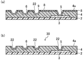
도 1에 나타내는 바와 같이, 본 실시형태의 프린트 배선기판(1)은, 제 1 수지층(2)과, 제 1 수지층(2) 상에 형성된 도체회로(3)와, 제 1 수지층(2) 상에서 도체회로(3)를 피복하도록 형성된 제 2 수지층(4)과, 제 2 수지층(4)에 형성된 비아홀(5) 및 트렌치(6)와, 비아홀(5) 및 트렌치(6)에 형성된 금속층(7)을 구비한다.1, the printed
제 1 수지층(2)은, 프린트 배선기판(1)의 베이스 기판으로서의 역할을 갖는 것이며, 전기적 절연성을 갖는 수지 재료에 의해 형성된다. 제 1 수지층(2)을 형성하는 재료로서는, 예를 들어, 에폭시 수지(epoxy resin), 폴리이미드 수지(polyimide resin), 비스말레이미드-트리아진 수지(bismaleimide-triazine resin), 폴리페닐렌에테르 수지(polyphenyleneether resin), 액정 폴리머, 폴리에테르에테르케톤 수지(polyether ether ketone resin), 폴리에테르이미드 수지(polyetherimide resin), 폴리에테르술폰 수지(polyether sulfone resin) 등을 들 수 있다.The
또, 연속 다공질(多孔質) 폴리테트라플루오로에틸렌 수지(polytetrafluoroethylene resin) 등의 3차원 망상구조(three-dimensional network)의 불소계 수지 기재에 에폭시 수지 등의 열경화성(熱硬化性) 수지를 함침(含浸)시킨 수지-수지 복합재료로 이루어진 판재(板材) 등을 사용하여도 된다.In addition, a fluorine-based resin substrate of a three-dimensional network such as a continuous porous polytetrafluoroethylene resin is impregnated with a thermosetting resin such as an epoxy resin ) Made of a resin-resin composite material or the like may be used.
도체회로(3)는, 프린트 배선기판(1)의 배선패턴을 형성하는 금속 회로이며, 제 1 수지층(2) 상에 붙이거나, 또는 제 1 수지층(2)에 대해 도금처리를 실시함으로써 형성된다.The
도체회로(3)는, 예를 들어, 구리, 알루미늄, 철, 니켈, 크롬, 몰리브덴 등의 금속박(箔), 또는 이들의 합금박(예를 들어, 알루미늄청동, 인청동(燐靑銅), 황청동(黃靑銅) 등의 구리합금이나, 스테인리스, 호박(amber), 니켈합금, 주석합금 등)에 의해 구성된다.The
또한, 도체회로(3)로서, 이들의 금속박 등을 단층 또는 복수층으로 적층한 것을 사용할 수 있으며, 특히, 도금 밀착성 및 전기 전도성을 향상시키며, 비용을 저하시키는 관점에서, 구리 또는 구리합금을 사용하는 것이 바람직하다.As the
제 2 수지층(4)은, 제 1 수지층(2)의 표면 상에 형성된 도체회로(3)를 보호하는 역할을 갖는 것이다. 이 제 2 수지층(4)을 형성하는 재료로서는, 상술의 제 1 수지층(2)을 형성하는 재료와 마찬가지 재료를 사용할 수 있다.The
또한, 무전해 도금처리 시에, 도금액에 대한 유해물질이 용출(溶出)되지 않으며, 계면박리를 발생시키지 않는 등의, 도금 처리공정에 대한 내성(耐性)을 가짐과 동시에, 도체회로(3)와의 밀착성을 향상시키고, 제 1 및 제 2 수지층(2, 4)의 밀착성도 향상시켜, 냉열 사이클 등의 시험에서의 박리나 크랙(crack) 등의 발생을 회피하는 관점에서, 제 1 및 제 2 수지층(2, 4)으로서, 에폭시 수지를 사용하는 것이 바람직하다.In addition, in the electroless plating process, the harmful substance to the plating liquid does not elute, and resistance to the plating process such as the occurrence of interface delamination does not occur, and at the same time, From the viewpoint of improving adhesion between the first and
금속층(7)은, 도금처리(무전해 도금처리)에 의해, 비아홀(5) 내 및 트렌치(6) 내에 도금용 금속을 충전함으로써 형성된다. 이 금속층(7)을 형성하는 금속으로서는, 예를 들어, 구리나 니켈 등을 들 수 있다.The
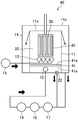
다음에, 도면을 참조하여, 본 실시형태의 무전해 도금장치를 설명한다. 도 2는, 본 발명의 제 1 실시형태에 관한 무전해 도금장치를 나타내는 도이다.Next, an electroless plating apparatus of the present embodiment will be described with reference to the drawings. 2 is a diagram showing an electroless plating apparatus according to a first embodiment of the present invention.
무전해 도금장치(10)는, 기판에 대해 도금처리(무전해 도금처리)를 행함으로써, 비아홀(5) 내 및 트렌치(6) 내에 도금 금속을 충전하여, 프린트 배선기판(1)의 회로를 구성하는 금속층(7)을 형성하기 위한 장치이다.The
이 무전해 도금장치(10)는, 도금액(20)이 충전된 도금조(11)와, 도금조(11) 내에 도금액(20)을 공급하는 도금액 공급수단(12)과, 도금조(11) 내에서 피(被)처리기판(30) 하방의 도금액(20) 내로 산소함유기체(즉, 기포)를 확산시키는 산기수단(air diffuser)(13)과, 도금조(11)로부터 오버플로우 된 도금액(20)을 저류하는 오버플로우조(overflow tank)(14)를 구비한다.This
도금조(11)는, 거의 직사각형 형상의 개구(11a)를 상면(上面)에 갖는 거의 직육면체 형상의 용기이며, 그 내부에는, 도금액(20)이 충전된다. 그리고, 도 2에 나타내는 바와 같이, 도금처리를 행하는 시에, 피처리기판(30) 전체가, 도금조(11)의 내부에 충전된 도금액(20)에 침지되는 구성이 된다.The
여기서, 도 2에 나타내는 바와 같이, 피처리기판(30)은, 도금조(11)의 상방에 배치된 지그(21)에 의해 파지(把持)된 상태에서, 그 전체가 도금액(20)에 침지되는 구성이 된다.2, the
이 지그(21)는, 피처리기판(30)의 외형보다 큰 테두리와, 테두리의 상변 및 하변에 배치되어 피처리기판(30)의 단부를 파지하는 클램프를 가지고, 상하방향 및 수평방향으로 이동 가능한 반송(搬送)장치(도시 않음)에 접속된다.The
또, 피처리기판(30)은, 거의 수직상태에서 도금액(20) 중에 침지되며, 피처리기판(30)의 표면과, 도금조(11)의 벽면이 거의 평행이 되도록 파지된다.The substrate to be processed 30 is immersed in the plating
도금액 공급수단(12)은, 도금조(11) 내에 있어서, 피처리기판(30)의 하방에 배치된다. 이 도금액 공급수단(12)은, 예를 들어, 복수의 액분출공(孔)을 가지며, 서로 수평으로 배치되고, 전체길이가 피처리기판(30)의 수평방향의 폭보다 길며, 또한, 피처리기판(30)으로부터의 거리가 등거리가 되는 위치에 배치된 2개의 관부재에 의해 구성된다. 따라서, 2개의 관부재는, 피처리기판(30)의 표리면 어느 쪽에 있어서도 액류(液流)의 효과를 높일 수 있다.The plating liquid supply means 12 is disposed below the
산기수단(13)은, 도금조(11) 내에 있어서, 피처리기판(30)의 하방에 배치된다. 이 산기수단(13)은, 도 2에 나타내는 바와 같이, 상술의 도금액 공급수단(12)에 인접하여 배치됨과 동시에, 산소함유기체를 산기수단(13)에 공급하기 위한 에어펌프(15)에 접속된다.The diffusing means 13 is disposed in the
이 산기수단(13)은, 예를 들어, 다공성 세라믹재료에 의해 형성된 2개의 관부재에 의해 구성된다. 이 2개의 관부재는, 서로 수평으로 배치되며, 또한, 피처리기판(30)으로부터의 거리가 등거리가 되는 위치에 배치되고, 피처리기판(30)의 표면에 대해, 충분한 산소함유기체를 공급할 수 있도록 구성된다. 그리고, 상술의 에어펌프(15)로부터, 산기수단(13)의 내부에 산소함유기체가 공급되면, 다공성 세라믹재료에 의해 형성된 다공체(多孔體)를 통하여, 산소함유기체가 도금액(20) 중으로 확산되는 구성이 된다.The diffusing means 13 is constituted by, for example, two pipe members formed of a porous ceramic material. These two pipe members are arranged horizontally to each other and are disposed at positions at equal distances from the
또한, 산기수단은, 장시간, 기체의 압력이 가해지므로, 예를 들어, 불소수지 등의 수지에 의해 형성되면, 도금액 중에서 파손되는 경우가 있으나, 본 실시형태에서는, 불소수지에 비해, 경도 및 내마모성이 우수한 다공성 세라믹재료에 의해 형성되므로, 도금액(20) 중의 산기수단(13)의 파손을 방지할 수 있다. 또, 다공체에 형성된 구멍에 오염물질 등이 부착된 경우에는, 세척함으로써, 산기수단(13)을 반복하여 사용할 수 있다.In addition, the diffusing means may be damaged in the plating liquid if formed by a resin such as a fluorine resin, for example, because the pressure of the gas is applied for a long period of time. In this embodiment, the hardness and wear resistance It is possible to prevent the breakage of the acid means 13 in the plating
또한, 트렌치(6)나 비아홀(5)의 내부로 기포가 들어가는 것을 방지함과 동시에, 도금액(20) 중의 용존산소량을 증가시키는 관점에서, 산소함유기체의 기포지름은, 5∼50㎛인 것이 바람직하다.It is preferable that the bubble diameter of the oxygen-containing gas is 5 to 50 占 퐉 in view of preventing the bubbles from entering the
또, 본 실시형태에서는, 환원반응의 진행에 기인하는 도금액(20)의 분해를 방지함과 동시에, 트렌치(6) 및 비아홀(5)의 도금 석출반응을 확실하게 개시시키는 관점에서, 무전해 도금을 개시(즉, 도금액(20) 중으로 피처리기판(30) 전체가 침지완료)하기 전에, 소정 시간(예를 들어, 1∼2분간), 산기수단(13)에 의한 확산처리를 행하지 않는 것이 바람직하다.From the viewpoint of preventing the decomposition of the plating
또한, 도금액(20) 중의 용존산소량 증가에 기인하여, 트렌치(6)의 내부 및 비아홀(5)의 내부의 도금 석출이 억제되는 문제를 회피함과 동시에, 도금액(20) 중의 용존산소량 저하에 기인하여, 트렌치(6) 외와 비아홀(5) 외 부분에서 도금이 석출되는 문제를 확실하게 방지하는 관점에서, 도금액(20)에 대한 산소함유기체의 공급속도는, 도금액 1L당 0.1∼1.0L/분이 바람직하다.It is also possible to avoid the problem that deposition of plating on the inside of the
오버플로우조(14)는, 도금조(11)에 인접하여 배치되며, 도금조(11)의 상단의 개구(11a)를 사이에 두고, 대치하는 양측부분(즉, 평면에서 보아, 거의 직사각형 형상을 이루는 도금조(11)의 4개의 측벽부 중, 대치하는 2개의 측벽부의 상단부)에 배치된다.The
그리고, 도금조(11)에 충전된 도금액(20)은, 도금조(11)에 형성된 유출구(11b)를 통하여, 오버플로우조(14)로 오버플로우 되어, 오버플로우조(14)의 내부에 저류되는 구성이 된다.The plating
또, 도 2에 나타내는 바와 같이, 무전해 도금장치(10)는, 도금조(11), 및 오버플로우조(14)에 접속되어, 오버플로우조(14)의 내부에 저류된 도금액을, 도금조(11)에 도입하기 위한 순환로(16)와, 순환로(16)에 설치된 펌프(17), 온도조절수단(18), 및 필터(19)를 구비한다.2, the
그리고, 오버플로우조(14)에 저류된 도금액(20)은, 펌프(17)에 의해, 순환로(16)로 도입되어, 온도조절수단(18)에 의한 온도조절, 및, 필터(19)에 의한 이물(異物) 등의 제거가 이루어진 후, 순환로(16)에 의해 순환되어, 도금조(11) 내에 도입된다. 이와 같은 구성에 의해, 도금조(11)의 내부에서, 도금액(20)의 강한 상승액류(즉, 도금조(11)의 하부로부터 상부로 향하는 강한 액류)가 형성되는 구성이 된다.The plating
또한, 도금조(11)의 하부에는, 배출구(24)가 형성되고, 배출구(24)로부터 배출된 도금액(20)은, 상술의 순환로(16)에 접속된 배출로(23)를 통하여, 순환로(16)로 도입되어, 상술의 오버플로우조(14)의 내부에 저류된 도금액(20)과 마찬가지로, 온도조절수단(18)에 의한 온도조절, 및, 필터(19)에 의한 이물 등의 제거가 이루어진 후, 순환로(16)에 의해 순환되어, 도금조(11) 내에 도입된다. 이와 같은 구성에 의해, 도금조(11)의 바닥부에 축적되는 이물을 제거하는 것이 가능해진다.The plating
다음에, 본 실시형태의 프린트 배선기판의 제조방법에 대해 일례를 들어 설명한다. 도 3, 도 4는, 본 발명의 제 1 실시형태에 관한 프린트 배선기판의 제조방법을 설명하기 위한 단면도이다. 그리고, 본 실시형태의 제조방법은, 도체회로 형성공정, 제 2 수지층 형성공정, 보호층 형성공정, 비아홀·트렌치 형성공정, 도금 전(前)처리공정, 촉매 부여공정, 보호층 박리공정, 및 도금 처리공정을 구비한다.Next, a manufacturing method of the printed wiring board of the present embodiment will be described with an example. 3 and 4 are cross-sectional views for explaining a method of manufacturing a printed wiring board according to the first embodiment of the present invention. The manufacturing method of the present embodiment is a method of manufacturing a semiconductor device including a conductor circuit forming step, a second resin layer forming step, a protective layer forming step, a via hole / trench forming step, a pre- And a plating process.
<도체회로 형성공정>≪ Conductor Circuit Forming Step &
먼저, 예를 들어, 에폭시 수지로 이루어진 제 1 수지층(2)의 표면 상에, 예를 들어, 구리박(두께: 수㎛∼25㎛)을 붙여, 제 1 수지층(2)의 표면 상에 구리박 적층판(copper clad laminated)을 형성한다. 이어서, 이 구리박 적층판을, 포토리소그래피나 스크린 인쇄 등의 방법에 의해 패터닝하여, 도 3(a)에 나타내는 바와 같이, 제 1 수지층(2)의 표면 상에 도체회로(3)를 형성한다.First, a copper foil (thickness: several mu m to 25 mu m), for example, is adhered on the surface of the
또한, 상술한 구리박 적층판은, 제 1 수지층(2)에 대해, 구리박을 도금처리함으로써 형성하여도 된다.The above-mentioned copper-clad laminated sheet may be formed by plating a copper foil with respect to the first resin layer (2).
<제 2 수지층 형성공정>≪ Second resin layer forming step &
다음에, 예를 들어, 에폭시 수지(두께: 20㎛∼100㎛)를, 도체회로(3)를 피복하도록 제 1 수지층(2) 상에 형성하고, 이 에폭시 수지에 대해 가열·가압처리(예를 들어, 온도: 100∼300℃, 압력: 5∼60㎏/㎠)를 행함으로써, 도 3(b)에 나타내는 바와 같이, 제 1 수지층(2) 상에 도체회로(3)를 피복하도록 에폭시 수지로 이루어진 제 2 수지층(4)을 형성한다.Next, for example, an epoxy resin (thickness: 20 to 100 m) is formed on the
또한, 접착제층(도시 않음)을 개재하여, 제 1 수지층(2) 상에 제 2 수지층(4)을 붙임으로써, 제 2 수지층(4)을 적층하여도 된다.The
<보호층 형성공정>≪ Protective layer forming step &
다음에, 예를 들어, 폴리이미드 수지(두께: 0.1㎛∼10㎛)를, 제 2 수지층(4) 상에 도포 후, 이 폴리이미드 수지에 대해 가열처리를 행함으로써, 도 3(c)에 나타내는 바와 같이, 제 2 수지층(4) 상에 폴리이미드 수지로 이루어진 보호층(8)을 형성한다.Next, a polyimide resin (thickness: 0.1 占 퐉 to 10 占 퐉) is coated on the
또한, 제 2 수지층(4) 상에 보호층(8)을 적층하는 시에, 먼저, 제 2 수지층(4) 상에 접착제층(도시 않음)을 적층시킨 후, 이 접착제층을 개재하여, 제 2 수지층(4) 상에 보호층(8)을 적층하여도 된다. 이 경우, 접착제층으로서, 예를 들어, 폴리아마이드 수지(polyamide resin), 폴리에스테르 수지(polyester resin), 폴리올레핀 수지(polyolefine resin), 폴리우레탄 수지(polyurethane resin) 등으로 이루어진 내열성의 접착시트 등을 사용할 수 있고, 이 접착시트를 가열에 의해 융착(融着)시켜, 접착제층을 형성한다. 또, 접착체층의 융착 조건으로서는, 특별히 한정되지 않고, 접착시트 등을 형성하는 수지에 따라, 적절히 변경할 수 있다. 예를 들어, 30초∼2분간, 100∼190℃ 정도로 가열함으로써, 접착시트를 융착시켜, 접착제층을 형성할 수 있다.When the
이 보호층(8)은, 후술하는 촉매 부여공정에서, 제 2 수지층(4)에 형성된 비아홀(5) 및 트렌치(6)에만 촉매를 부착시키고, 제 2 수지층(4)의 표면(4a)(도 1, 도 3(c) 참조)으로의 촉매 부착을 방지하기 위한 것이다.The
또, 이 보호층(8)은, 절연성, 및 발수성을 가짐과 동시에, 후술하는 보호층 박리공정에서 사용되는 박리액에 용해되는 수지에 의해 형성된다. 보호층(8)을 형성하는 수지로서는, 예를 들어, 폴리이미드 수지, 규소수지(silicone resin), 페놀수지(phenol resin), 크실렌수지(xylene resin), 불포화폴리에스테르 수지(unsaturated polyester resin), 디알릴프탈레이트 수지(diallylphthalate resin), 아크릴수지(acryl resin), 폴리카보네이트 수지(polycarbonate resin) 등의 알칼리 가용성(可溶性) 수지와, 아크릴수지, 페놀수지, ABS수지, 폴리이소부틸렌 수지(polyisobutylene resin) 등의 알코올 용해성 수지 등을 들 수 있다.The
또한, 보호층(8)의 두께는, 0.1㎛∼10㎛가 바람직하다. 이는, 보호층(8)의 두께가 0.1㎛ 미만의 경우는, 후술하는 촉매 부여공정에서, 비아홀(5) 및 트렌치(6)에만 촉매를 부착시키고, 제 2 수지층(4)의 표면(4a)으로 촉매가 부착되는 것을 방지하는 기능이 저하되는 경우가 있기 때문이다. 또, 보호층(8)의 두께가 10㎛보다 큰 경우는, 보호층(8)에 형성되는 트렌치(6)의 깊이가 깊어지므로, 트렌치 폭이 좁은 프린트 배선기판(1)에 있어서, 트렌치(6) 형성이 곤란해지는 경우가 있기 때문이다.The thickness of the
<비아홀·트렌치 형성공정>≪ Via hole trench formation process >
다음에, 도 3(d)에 나타내는 바와 같이, 제 2 수지층(4) 상에 형성된 보호층(8)에 관통공(9)을 형성함과 동시에, 이 관통공(9)을 개재하여, 보호층(8)이 적층된 제 2 수지층(4)에, 비아홀(5), 및 트렌치(6)를 형성한다.3 (d), a through
이 비아홀(5), 트렌치(6), 및 관통공(9)을 형성하는 방법으로서는, 특별히 한정되지 않고, 예를 들어, 에칭 처리나 레이저 처리 등을 들 수 있다. 이 중, 미세한 형상을 갖는 비아홀(5) 등을 신속하게 형성하며, 에칭 처리의 노광(露光)·현상(現像)에 의한 위치 어긋남이나 현상불량 등의 문제를 방지하고, 또한, 배선기판의 소형화·박형화와 더불어 미세화에 대응하여, 신뢰성 높은 배선패턴을 형성하는 관점에서, 레이저 처리에 의해 비아홀(5) 등을 형성하는 것이 바람직하다.The method of forming the via
또, 이 레이저 처리에 의해 비아홀(5) 등을 형성하는 경우, 레이저로서는, 예를 들어, CO2 레이저, YAG 레이저, 엑시머 레이저(excimer laser) 등의 일반적인 레이저를 사용할 수 있다. 또한, 아르곤 레이저(argon laser), 헬륨-네온 레이저(helium-neon laser) 등의 기체 레이저, 사파이어 레이저 등의 고체 레이저, 색소 레이저, 반도체 레이저, 자유 전자 레이저(free electron laser) 등을 사용하여도 된다. 이 중, 특히, 한층 더 미세한 형상을 갖는 비아홀(5) 등을 형성하는 관점에서, YAG 레이저나 엑시머 레이저 등을 사용하는 것이 바람직하다.In the case of forming the via
또, 비아홀(5)이나 트렌치(6)의 종횡비(aspect ratio), 직경의 크기, 깊이 등은, 프린트 배선기판(1)의 종류 등에 따라, 적절히 변경할 수 있다. 예를 들어, 비아홀(5)의 직경은 10∼200㎛, 비아홀(5)의 깊이는 2∼20㎛, 트렌치(6)의 폭은 1∼500㎛, 트렌치(6)의 깊이는 2∼20㎛로 설정할 수 있다.The aspect ratio, diameter, depth, etc. of the via
<도금 전(前)처리공정>≪ Pre-plating treatment step >
이어서, 상술의 비아홀(5), 및 트렌치(6)가 형성된 기판에 대해, 소정의 도금 전처리를 행한다. 보다 구체적으로는, 예를 들어, 청정용액(cleaning solution)(산성용액이나 중성액) 중에 65℃에서 5분간, 기판을 침지시켜, 기판 표면, 비아홀(5), 및 트렌치(6)의 먼지 등을 제거한다. 이 청정처리에 의해, 비아홀(5)과 트렌치(6)의 내부를 세척하여, 후(後)공정에서 형성되는 도금피막의 밀착성 등을 향상시킨다.Then, a predetermined plating pretreatment is performed on the above-described via
또한, 비아홀(5)의 바닥부에서 노출된 도체회로(3)의 표면에 대해 활성화 처리를 행하여도 된다. 이 활성화 처리는, 예를 들어, 황산이나 염산의 10% 용액으로 이루어진 산성용액 등을 이용하여, 산성용액 중에 기판을 5∼10초간 침지시켜 행한다. 이와 같이, 기판을 산성용액에 침지함으로써, 활성화 영역인 도체회로(3)의 표면에 잔존한 알칼리 물질을 중화하여, 얇은 산화막을 용해시킬 수 있다.The surface of the
<촉매 부여공정>≪ Catalyst applying step &
다음에, 도 4(a)에 나타내는 바와 같이, 제 2 수지층(4)에 촉매(22)를 부여하여, 제 2 수지층(4)에 형성된 비아홀(5) 및 트렌치(6)에 촉매(22)를 부착시킨다.4 (a), a
본 공정은, 예를 들어, 2가(價)의 팔라듐 이온(Pd2+)을 함유한 촉매액을 이용하여 행할 수 있다. 또, 이 경우의 촉매액으로서는, 예를 들어 Pd 농도가 100∼300㎎/l의 염화팔라듐(PdCl2·2H2O)과, Sn 농도가 10∼20g/l의 염화제1주석(SnCl2·2H2O)과, 150∼250ml/l의 염산(HCl)을 함유하는 혼합액을 사용할 수 있다.This step can be carried out using, for example, a catalyst liquid containing a divalent palladium ion (Pd 2+ ). As the catalyst solution in this case, for example, palladium chloride (PdCl 2 .2H 2 O) having a Pd concentration of 100 to 300 mg / l and stannous chloride (SnCl 2 2H 2 O) and hydrochloric acid (HCl) at 150 to 250 ml / l can be used.
촉매(22) 부여는, 먼저, 도 3(d)에 나타내는 기판을, 촉매액 중에, 예를 들어, 온도 30∼40℃의 조건에서 1∼3분간 침지시켜, Pd-Sn 콜로이드(colloid)를 기판 표면에 흡착(吸着)시킨다. 다음에, 상온(常溫) 조건 하에서, 50∼100ml/l의 황산 또는 염산으로 이루어진 악셀러레이터(accelerator)(촉진제)에 기판을 침지시켜, 촉매 활성화를 행한다. 이 활성화 처리에 의해, 착화합물(錯化合物)의 주석이 제거되어, 팔라듐 흡착입자가 되고, 최종적으로 팔라듐 촉매로서, 무전해 도금처리에 의한 금속도금의 석출을 촉진시키게 된다.3 (d) is immersed in the catalyst liquid at a temperature of, for example, 30 to 40 ° C for 1 to 3 minutes to form a Pd-Sn colloid (Adsorbed) onto the substrate surface. Subsequently, the substrate is immersed in an accelerator (accelerator) composed of 50 to 100 ml / l of sulfuric acid or hydrochloric acid under a normal temperature condition to perform catalyst activation. By this activation treatment, the tin of the complex compound (complex compound) is removed to form palladium-adsorbed particles, and as a palladium catalyst, the precipitation of the metal plating by the electroless plating treatment is promoted.
그리고, 촉매(22)로서, 구리이온(Cu2+)을 함유한 촉매액을 이용하여 행하여도 된다. 또, 주석을 함유하지 않는 산성 콜로이드 타입, 또는 알칼리 이온 타입의 촉매액을 이용할 수도 있다. 또한, 상술의 악셀러레이터로서, 수산화나트륨이나 암모니아 용액을 사용하여도 된다.As the
또, 컨디셔너액이나 프리딥(pre-dip)액을 이용하여, 비아홀(5) 및 트렌치(6)에서의 제 2 수지층(4)과 금속층(7)과의 밀착성을 높이는 전(前)처리를 실시하여도 된다. 또한, 예를 들어, 기판에 대해, 촉매액을 스프레이 방식에 의해 분사하여 접촉시킴으로써, 촉매를 부여하는 구성으로 하여도 된다.It is also possible to use a conditioner liquid or a pre-dip liquid to perform a pretreatment for increasing the adhesion between the
<보호층 박리공정>≪ Protection layer peeling step &
이어서, 박리액을 사용하여, 도 4(b)에 나타내는 바와 같이, 제 2 수지층(4)의 표면(4a) 상에 형성된 보호층(8)의 박리를 행한다. 보다 구체적으로는, 박리액 중에, 도 4(a)에 나타내는 촉매(22)가 부여된 기판을 침지시켜, 보호층(8)을 박리액에 용해시킴으로써, 제 2 수지층(4)의 표면(4a) 상에 형성된 보호층(8)을 박리한다.Then, the
사용하는 박리액으로서는, 박리되는 보호층(8)을 형성하는 수지의 종류에 따라, 적절히 변경할 수 있다. 예를 들어, 상술의 폴리이미드 수지나 규소수지 등의 알칼리 수용액에 가용(可溶)인 수지에 의해 보호층(8)을 형성한 경우는, 박리액으로서, 수산화나트륨 수용액이나 수산화칼륨 수용액 등의 수산화 알칼리 금속수용액을 사용할 수 있다. 또, 상술의 아크릴수지, 페놀수지 등의 알코올 용액에 가용인 수지에 의해 보호층(8)을 형성한 경우는, 박리액으로서, 이소프로필알코올(isopropyl alcohol) 등의 알코올 용액을 사용할 수 있다.The exfoliation liquid to be used may be appropriately changed depending on the type of the resin forming the
또, 비아홀(5) 및 트렌치(6)에 부착된 촉매(22)의 제거를 방지하여, 후술하는 도금처리의 도금의 미석출을 방지하는 관점에서, 본 공정에서는, 박리액 중에 기판(즉, 보호층(8))을 침지시켜, 보호층(8)을 박리하는 방법이 채용된다.From the viewpoint of preventing the removal of the
그리고, 박리액으로의 보호층(8)의 침지시간은, 보호층(8)을 형성하는 수지나 박리액의 농도 등에 따라, 적절히 변경할 수 있다. 예를 들어, 폴리이미드 수지에 의해 형성된 보호층(8)을, 농도가 0.4㏖/l인 수산화나트륨 수용액을 사용하여 박리하는 경우, 침지시간을 30초 이상 120초 이하로 설정할 수 있다. 이와 같이, 사용하는 박리액의 농도에 대응시켜 침지시간을 설정함으로써, 비아홀(5) 및 트렌치(6)에 부착된 촉매(22)의 제거를 확실하게 방지하며, 보호층(8)의 박리를 행하는 것이 가능해진다.The immersion time of the
또한, 비아홀(5) 및 트렌치(6)에만 촉매(22)를 부착시키고, 트렌치(6) 외와 비아홀(5) 외 부분으로의 촉매(22)의 부착을 방지하기 위해, 상술의 보호층(8) 대신에, 제 2 수지층(4) 상에 마스킹테이프를 붙이고, 촉매 부여공정 후, 이 마스킹테이프를 박리하는 방법을 채용하여도 된다.In order to attach the
<도금 처리공정>≪ Plating process step &
이어서, 도 4(b)에 나타내는 촉매(22)가 부여된 기판(즉, 피처리기판(30))에 대해, 도금처리(무전해 도금처리)를 행하여, 촉매(22)가 부착된 비아홀(5) 내 및 트렌치(6) 내에 도금 금속을 충전함으로써, 프린트 배선기판(1)의 회로를 구성하는 금속층(7)을 형성한다.Subsequently, a plating process (electroless plating process) is performed on the substrate to which the
여기서, 본 공정에서 사용되는 무전해 도금액은, 수용성 제2구리(합금)염이나 수용성 니켈(합금)염 등의 수용성 금속염을 주성분으로 하고, 포름알데히드(formaldehyde)나 파라포름알데히드(paraformaldehyde), 글리옥실산(glyoxylic acid) 또는 그 염, 차아인산(hypophosphorous acid) 또는 그 염, 디메틸아미노보란(dimethylaminoborane) 등 1종 이상의 환원제와, 에틸렌 디아민4아세트산4나트륨(tetra-sodium ethylenediaminetetraacetate)이나 주석산나트륨칼륨(potassium sodium tartrate) 등의 착화제를 함유함과 동시에, 적어도 1종의 유황계 유기화합물을 레벨러로서 함유한다.Here, the electroless plating solution used in the present step is a solution containing a water-soluble metal salt such as a water-soluble second copper (alloy) salt or a water-soluble nickel (alloy) salt as a main component and a formaldehyde, paraformaldehyde, At least one reducing agent such as glyoxylic acid or its salt, hypophosphorous acid or its salt or dimethylaminoborane and at least one reducing agent such as tetra-sodium ethylenediaminetetraacetate or potassium sodium tartrate potassium sodium tartrate) and at least one kind of sulfur-based organic compound as a leveler.
또, 무전해 도금액은, 주성분으로서, 수용성 제2구리염이나 수용성 니켈염 등의 수용성 금속염을 함유한다. 수용성 금속염으로서 수용성 제2구리염 또는 수용성 니켈염을 함유시킴으로써, 각각 무전해 구리도금액 또는 무전해 니켈도금액을 생성한다.The electroless plating solution contains, as a main component, a water-soluble metal salt such as a water-soluble cupric salt or a water-soluble nickel salt. By containing a water-soluble cupric salt or a water-soluble nickel salt as a water-soluble metal salt, an electroless copper plating solution or an electroless nickel plating solution is produced, respectively.
수용성 제2구리염으로서는, 예를 들어, 황산구리, 염화구리, 질산구리, 아세트산구리, EDTA구리 등을 이용할 수 있으며, 이들 수용성 제2구리염을 적어도 1종 포함하거나, 또는 임의의 비율로 2종 이상을 함유시켜도 된다. 이 수용성 제2구리염의 농도로서는, 0.001mol/L∼0.2mol/L가 바람직하다. 그리고, 금속이온원으로서 구리를 함유시키는 경우, 수용성 제2구리염을 함유시키는 것에 한정되지 않고, 그 밖의 금속염을 함유시켜 무전해 구리합금 도금액을 생성하도록 하여도 된다.As the water-soluble cupric salt, for example, copper sulfate, copper chloride, copper nitrate, copper acetate, EDTA copper and the like can be used, and at least one of these water- Or more. The concentration of the water-soluble cupric salt is preferably 0.001 mol / L to 0.2 mol / L. When copper is contained as a metal ion source, the electrolytic copper alloy plating liquid may be produced by adding other metal salts to the plating solution, not limited to a solution containing a water-soluble cupric salt.
수용성 니켈염으로서는, 예를 들어, 염화니켈, 황산니켈, 질산니켈, 아세트산니켈, 차아인산니켈 등의 유기니켈염 등을 이용할 수 있으며, 이들 수용성 니켈염을 적어도 1종 포함하거나, 또는 임의의 비율로 2종 이상을 함유시켜도 된다. 이 수용성 니켈염의 농도로서는, 0.001mol/L∼0.2mol/L가 바람직하다. 그리고, 금속이온원으로서 니켈을 함유시키는 경우, 수용성 니켈염을 함유시키는 것에 한정되지 않고, 그 밖의 금속염을 함유시켜 무전해 니켈합금 도금액을 생성하도록 하여도 된다.As the water-soluble nickel salt, there can be used, for example, an organic nickel salt such as nickel chloride, nickel sulfate, nickel nitrate, nickel acetate, nickel hypophosphite and the like, and it is possible to use at least one of these water soluble nickel salts, Or two or more of them may be contained. The concentration of the water-soluble nickel salt is preferably 0.001 mol / L to 0.2 mol / L. When nickel is contained as a metal ion source, it is not limited to containing a water soluble nickel salt, and other metal salts may be contained to produce an electroless nickel alloy plating liquid.
환원제로서는, 포름알데히드, 파라포름알데히드, 글리옥실산 또는 그 염, 차아인산 또는 그 염, 디메틸아미노보란 등의 공지의 환원제를 이용할 수 있으며, 이들 환원제를 적어도 1종 포함하거나, 또는 임의의 비율로 2종 이상을 함유시켜도 된다. 이 환원제의 농도로서는, 0.01mol/L∼0.5mol/L가 바람직하다.As the reducing agent, known reducing agents such as formaldehyde, paraformaldehyde, glyoxylic acid or a salt thereof, hypophosphoric acid or its salt, dimethylaminoborane and the like can be used, and at least one kind of these reducing agents may be contained, Two or more species may be added. The concentration of the reducing agent is preferably 0.01 mol / L to 0.5 mol / L.
착화제로서는, 폴리아민(polyamine), 폴리알카놀아민(polyalkanolamine), 폴리아미노폴리카르복시산(polyaminopolycarboxylic acid) 또는 그 염, 카르복시산 또는 그 염, 옥시카르복시산(oxycarboxylic acid) 또는 그 염, 아미노산 또는 그 염 등을 이용할 수 있으며, 이들 착화제를 적어도 1종 포함하거나, 또는 임의의 비율로 2종 이상을 함유시켜도 된다. 이 착화제를 무전해 도금액에 함유시킴으로써, 알칼리성의 도금액 중에서도, 상술한 구리이온이나 니켈이온 등의 금속이온을 안정되게 유지시킨다.Examples of the complexing agent include polyamine, polyalkanolamine, polyaminopolycarboxylic acid or a salt thereof, a carboxylic acid or a salt thereof, an oxycarboxylic acid or a salt thereof, an amino acid or a salt thereof, And at least one of these complexing agents may be contained, or two or more kinds of these complexing agents may be contained in an arbitrary ratio. By containing this complexing agent in the electroless plating solution, metal ions such as copper ions and nickel ions described above are stably maintained in the alkaline plating solution.
보다 구체적으로, 폴리아민으로서는, 에틸렌디아민(ethylenediamine), 트리에틸렌테트라민(triethylenetetramine), 헥사메틸렌테트라민(hexamethylenetetramine), 펜타에틸렌헥사민(pentaethylenehexamine) 등을 들 수 있다. 또, 폴리알카놀아민으로서는, 트리에탄올아민(triethanolamine), 디에탄올아민(diethanolamine), 트리이소프로판올아민(triisopropanolamine) 등을 들 수 있다. 또한, 폴리아미노폴리카르복시산으로서는, 에틸렌디아민4아세트산(EDTA), 니트릴로3아세트산디에틸렌트리아민5아세트산 등, 또는 이들의 염을 들 수 있다. 또, 옥시카르복시산으로서는, 구연산, 주석산, 글루콘산, 사과산 등, 또는 이들의 염을 들 수 있다. 또한, 아미노산으로서는, 글리신(glycine), 글루탐산(glutamic acid) 등, 또는 이들의 염을 들 수 있다.More specifically, examples of polyamines include ethylenediamine, triethylenetetramine, hexamethylenetetramine, pentaethylenehexamine, and the like. Examples of the polyalkanolamine include triethanolamine, diethanolamine, triisopropanolamine, and the like. Examples of the polyaminopolycarboxylic acid include ethylenediaminetetraacetic acid (EDTA), diethylenetriamineacetate triethylacetate, and salts thereof. Examples of the oxycarboxylic acid include citric acid, tartaric acid, gluconic acid, and malic acid, and salts thereof. Examples of amino acids include glycine, glutamic acid, and salts thereof.
그리고, 본 실시형태에 관한 무전해 도금액에 함유되는 착화제로서는, 특히, 에틸렌디아민4아세트산4나트륨(EDTA-4Na), 주석산나트륨칼륨(로셸염), 하이드록시에틸에틸렌디아민3아세트산3나트륨(HEDTA) 등을 적합하게 이용할 수 있다. 그 착화제의 농도로서는, 0.01mol/L∼1mol/L 함유시키는 것이 바람직하고, 착화제의 합계농도가 수용성 금속염의 1∼5배의 몰량이 되도록 함유시키는 것이 바람직하다.As the complexing agent contained in the electroless plating solution according to the present embodiment, particularly preferred are tetrasodium ethylenediaminetetraacetate (EDTA-4Na), sodium potassium tartrate (Rochelle salt), trisodium hydroxyethylethylenediamine triacetate (HEDTA ) Can be suitably used. The concentration of the complexing agent is preferably 0.01 mol / L to 1 mol / L, and it is preferable that the total concentration of the complexing agent is 1 to 5 times the molar amount of the water-soluble metal salt.
본 실시형태에 관한 무전해 도금액에서는, 레벨러로서, 적어도 1종의 유황계 유기화합물을 함유하는 것을 특징으로 한다. 본 실시형태에 관한 무전해 도금액에 함유되는 유황계 유기화합물은, 탄소원자, 산소원자, 인원자, 유황원자, 질소원자를, 각각 임의의 수로 포함하는 지방족 환상기 또는 방향족 환상기, 또는 이들 환상기에 임의의 1종류 이상의 치환기가 하나 이상 결합한 환상기를, 적어도 하나 포함하는 화합물이다.The electroless plating solution according to the present embodiment is characterized in that it contains at least one sulfur-based organic compound as a leveler. The sulfur-based organic compound contained in the electroless plating solution according to the present embodiment is an aliphatic cyclic group or an aromatic cyclic group containing an arbitrary number of carbon atoms, oxygen atoms, phosphorus atoms, sulfur atoms and nitrogen atoms, Is a compound containing at least one cyclic group in which one or more arbitrary one or more substituents are bonded to the group.
구체적으로, 본 실시형태에 함유되는 유황계 유기화합물은, 하기 일반식(I) 내지 (V) 중 어느 것에 의해 나타내는 적어도 1종의 화합물이다.Specifically, the sulfur-based organic compound contained in the present embodiment is at least one kind of compound represented by any one of the following general formulas (I) to (V).
R1-(S)n-R2 (I)R 1 - (S) n -R 2 (I)
R1-L1-(S)n-R2 (II)R 1 -L 1 - (S) n -R 2 (II)
R1-L1-(S)n-L2-R2 (III)R 1 -L 1 - (S) n -L 2 -R 2 (III)
R1-(S)n-L3 (IV)R 1 - (S) n -L 3 (IV)
R1-L1-(S)n-L3 (V)R 1 -L 1 - (S) n -L 3 (V)
여기서, 상기 일반식(I)∼(V)에 있어서, n은, 1 이상의 정수이다. 또, R1, R2는, 각각 독립적으로 탄소원자, 산소원자, 인원자, 유황원자, 질소원자를, 각각 임의의 수로 포함하는 지방족 환상기 또는 방향족 환상기, 또는 이 환상기에 임의의 1종류 이상의 치환기가 하나 이상 결합한 환상기이다. 또, L1, L2는, 각각 독립적으로 직쇄 또는 분기된 알킬쇄, 알킬아미노쇄, 알킬렌쇄, 알콕시쇄로 이루어진 군 중 어느 하나이다. 또한, L3은, 알킬기, 알킬렌기, 아미노기, 알킬아미노기, 알킬렌아미노기, 하이드록시기, 알킬하이드록시기, 알킬렌하이드록시기, 카르복시기, 알킬카르복시기, 알킬렌카르복시기, 알킬아미노카르복시기, 알킬렌아미노카르복시기, 니트로기, 알킬니트로기, 니트릴기, 알킬니트릴기, 아마이드기, 알킬아마이드기, 카르보닐기, 알킬카르보닐기, 술폰산기, 알킬술폰산기, 포스폰산기, 알킬포스폰산기, 술파닐일기, 술피닐기, 티오카르보닐기로 이루어진 군 중 어느 하나이다.In the general formulas (I) to (V), n is an integer of 1 or more. R 1 and R 2 each independently represent an aliphatic cyclic group or aromatic cyclic group containing an arbitrary number of carbon atoms, an oxygen atom, a phosphorus atom, a sulfur atom and a nitrogen atom, or an arbitrary one kind Or a cyclic group in which one or more of the above substituents is bonded. L 1 and L 2 are each independently any one selected from the group consisting of straight chain or branched alkyl chain, alkylamino chain, alkylene chain and alkoxy chain. L 3 represents an alkyl group, an alkylene group, an amino group, an alkylamino group, an alkyleneamino group, a hydroxyl group, an alkylhydroxy group, an alkylenehydroxy group, a carboxyl group, an alkylcarboxy group, an alkylene carboxy group, A sulfonyl group, an alkylsulfonic acid group, a phosphonic acid group, an alkylphosphonic acid group, a sulfanyl group, a sulfo group, a sulfo group, an alkyl group, A thiocarbonyl group, or a thiocarbonyl group.
상기 일반식(I)∼(V) 중 R1, R2의 치환기로서는, 알킬기, 알킬렌기, 아미노기, 알킬아미노기, 알킬렌아미노기, 하이드록시기, 알킬하이드록시기, 알킬렌하이드록시기, 카르복시기, 알킬카르복시기, 알킬렌카르복시기, 알킬아미노카르복시기, 알킬렌아미노카르복시기, 니트로기, 알킬니트로기, 니트릴기, 알킬니트릴기, 아마이드기, 알킬아마이드기, 카르보닐기, 알킬카르보닐기, 술폰산기, 알킬술폰산기, 포스폰산기, 알킬포스폰산기, 술파닐일기, 술피닐기, 티오카르보닐기 등을 들 수 있다.Examples of the substituent of R 1 and R 2 in the general formulas (I) to (V) include alkyl groups, alkylene groups, amino groups, alkylamino groups, alkyleneamino groups, hydroxyl groups, alkylhydroxy groups, alkylenehydroxy groups, An amide group, an alkylamido group, a carbonyl group, an alkylcarbonyl group, a sulfonic acid group, an alkylsulfonic acid group, an alkylsulfonic acid group, an alkylsulfonic acid group, an alkylsulfonic acid group, A phosphonic acid group, an alkylphosphonic acid group, a sulfanyl group, a sulfinyl group, and a thiocarbonyl group.
또, 상기 환상기로서는, 페닐기(phenyl group), 나프틸기(naphthyl group), 푸르푸릴기(furfuryl group), 피리딜기(pyridyl group), 티아졸일기(thiazolyl group), 벤조티아졸일기(benzothiazolyl group), 피리미딘일기(pyrimidyl group), 이미다졸릴기(imidazolyl group), 티오페닐기(thiophenyl group) 등을 들 수 있다.Examples of the cyclic group include a phenyl group, a naphthyl group, a furfuryl group, a pyridyl group, a thiazolyl group, a benzothiazolyl group ), A pyrimidyl group, an imidazolyl group, a thiophenyl group, and the like.
그리고, 이와 같은 유황계 유기화합물로서는, 특별히 한정되는 것은 아니나, 그 일례로서, 2,2'-디피리딜디술피드(2,2'-dipyridyl disulfide), 2,2'-디벤조티아졸일디술피드(2,2'-dibenzothiazolyl disulfide), 3,3',5, 5'-테트라클로로디페닐디술피드(3,3',5,5'-tetrachlorodiphenyl disulfide), 2,2'-디티오비스(5-니트로피리딘)(2,2'-dithiobis(5-nitropyridine)), 2,2'-디티오디안식향산(2,2'-dithiodibenzoic acid), 2,2'-디티오디아닐린(2,2'-dithiodianiline), 5,5'-디티오비스(2-니트로안식향산)(5,5'-dithiobis(2-nitrobenzoic acid)), 4,4'-비스(2-아미노-6-메틸피리미딘일)디술피드(4,4'-bis(2-amino-6-methylpyrimidyl)disulfide), 4,4'-디피리딜술피드(4,4'-dipyridyl sulfide), 6,6'-디티오디니코틴산(6,6'-dithiodinicotinic acid), 2,2'-디티오디살리실산(2,2'-dithiodisalicylic acid), 디푸르푸릴술피드(difurfuryl sulfide), 비스(6-하이드록시-2-나프틸)디술피드(bis(6-hydroxy-2-naphthyl)disulfide), 푸르푸릴메틸디술피드(furfuryl methyl disulfide), 비스(2-벤즈아마이드페닐)디술피드(bis(2-benzamidephenyl)disulfide), 비스(3-하이드록시페닐)디술피드(bis(3-hydroxyphenyl)disulfide), 디에틸디티오카르밤산2-벤조티아졸일(diethyldithiocarbamic acid 2-benzothiazolyl), 5,5'-티오디살리실산(5,5'-thiodisalicylic acid), 5,5'-디티오디살리실산(5,5'-dithiodisalicylic acid), (4-피리딜티오)아세트산((4-pyridylthio)acetic acid), 3-(2-벤조티아졸일티오)프로피온산(3-(2-benzothiazolylthio)propionic acid), 4-(2-벤조티아졸일티오)모르폴린(4-(2-benzothiazolylthio)morpholine) 등을 들 수 있다. 특히, 2,2'-디피리딜디술피드, 6,6'-디티오디니코틴산, 2,2'-디티오디안식향산, 비스(6-하이드록시-2-나프틸)디술피드 등은, 트렌치와 비아홀 등에 대해 보다 양호하게 도금 금속을 충전할 수 있으며, 또 사용 가능한 농도범위도 넓고, 경시변화가 일어나기 어려워, 분해물의 영향이 적은 등, 이와 같은 관점에서, 적합하게 이용할 수 있다.Examples of such sulfur-based organic compounds include, but are not limited to, 2,2'-dipyridyl disulfide, 2,2'-dibenzothiazolyl disulfide, (3,3 ', 5,5'-tetrachlorodiphenyl disulfide), 2,2'-dithiobis (2,2'-dibenzothiazolyl disulfide) 5-nitropyridine), 2,2'-dithiodibenzoic acid, 2,2'-dithiodi aniline (2,2'- Dithiodianiline, 5,5'-dithiobis (2-nitrobenzoic acid), 4,4'-bis (2-amino-6-methylpyrimidinyl) (4,4'-dipyridyl sulfide), 6,6'-dithiodicotinic acid (6,4'-dipyridyl sulfide, , 6'-dithiodinicotinic acid, 2,2'-dithiodisalicylic acid, difurfuryl sulfide, Bis (6-hydroxy-2-naphthyl) disulfide, furfuryl methyl disulfide, bis (2-benzamidophenyl) disulfide bis (3-hydroxyphenyl) disulfide, diethyldithiocarbamic acid 2-benzothiazolyl, 5 (3-hydroxyphenyl) disulfide, , 5'-thiodisalicylic acid, 5,5'-dithiodisalicylic acid, (4-pyridylthio) acetic acid, (2-benzothiazolylthio) propionic acid, 4- (2-benzothiazolylthio) morpholine) and the like, . In particular, 2,2'-dipyridyl disulfide, 6,6'-dithiodinic acid, 2,2'-dithiodibenzoic acid, bis (6-hydroxy-2-naphthyl) It is possible to fill the plating metal more favorably with respect to the via hole and the like, and the usable concentration range is wide, the change with time is hard to occur, the influence of decomposition products is small, and the like.
이 유황계 유기화합물은, 0.001㎎/L∼500㎎/L의 농도범위로 함유시키는 것이 바람직하고, 보다 바람직하게는, 0.05㎎/L∼50㎎/L의 농도범위로 함유시킨다. 농도가 옅은 경우에는, 레벨러로서의 효과를 충분히 발휘시킬 수 없고, 농도가 진한 경우에는, 레벨러로서의 효과가 강하게 나타나 버려, 도금의 석출을 저해하거나, 기판 표면에 있어서도, 트렌치와 비아홀 내에서도, 도금피막의 막두께가 매우 얇아져 버려, 트렌치와 비아홀 내에 충분한 도금 금속을 충전할 수 없게 된다. 그 결과로서, 결함이 많은 프린트 배선기판이 형성되어 버린다. 따라서, 본 실시형태에 관한 무전해 도금액 중에 있어서는, 유황계 유기화합물을, 0.05㎎/L∼50㎎/L의 농도범위로 함유시키는 것이 바람직하고, 이 범위로 함유시킴으로써, 레벨러로서의 효과를 충분히 발휘시킴과 동시에, 양호하게 트렌치와 비아홀 내에 도금 금속을 충전할 수 있다.The sulfur-containing organic compound is preferably contained in a concentration range of 0.001 mg / L to 500 mg / L, more preferably 0.05 mg / L to 50 mg / L. When the concentration is low, the effect as a leveler can not be sufficiently exerted. When the concentration is high, the effect as a leveler is strongly exhibited, and the precipitation of the plating is inhibited, or even in the surface of the substrate or in the trench and the via hole, The film thickness becomes very thin, and sufficient plating metal can not be filled in the trench and the via hole. As a result, a printed wiring board having many defects is formed. Therefore, in the electroless plating solution according to the present embodiment, it is preferable that the sulfur-based organic compound is contained in a concentration range of 0.05 mg / L to 50 mg / L, and if it is contained in this range, At the same time, the plating metal can be filled in the trench and the via hole preferably.
이와 같은 유황계 유기화합물의 유황분자는, 금속과 강한 상호작용을 형성하여, 유황분자가 금속표면에 접하면 강하게 흡착하는 성질을 갖는다. 그리고, 이 유황계 유기화합물은, 금속이온과 함께 도금액 중을 확산되며, 촉매 중에 공급되나, 기판 표면에 비해, 도금액의 흐름이 약한 트렌치와 비아홀 등의 내부로의 공급량은, 기판 표면으로의 공급량에 비해 적어진다. 따라서, 트렌치 등의 바닥부에 가까워질수록, 유황계 유기화합물의 공급량은 적어지므로, 무전해 도금반응의 억제 작용은 작아지고, 결과적으로, 상향식 충전(bottom-up filling)이 진행되어, 트렌치 등의 내부에 보이드(void) 등의 결함을 발생시키는 일 없이 도금 금속을 충전하는 것이 가능해진다.The sulfur molecule of the sulfur-based organic compound has a property of forming a strong interaction with the metal and strongly adsorbing sulfur molecules when they come into contact with the metal surface. This sulfur-based organic compound diffuses in the plating solution together with metal ions and is supplied to the catalyst. However, the supply amount of trenches, via holes and the like into the interior of the substrate, in which the flow of the plating solution is weaker than the surface of the substrate, . Therefore, the closer to the bottom of the trench or the like the smaller the supply amount of the sulfur-based organic compound, the smaller the suppressing effect of the electroless plating reaction, and consequently the bottom-up filling progresses, It is possible to fill the plating metal without generating defects such as voids inside the plating metal.
또, 본 실시형태에 관한, 환상기를 갖는 유황계 유기화합물을 함유한 무전해 도금액에 의하면, 장시간, 보이드나 심(seam) 등의 결함 발생을 억제하고, 트렌치 등에 대해 양호한 도금 충전성을 발휘시킬 수 있다.According to the electroless plating solution containing a sulfur-containing organic compound having a cyclic structure according to the present embodiment, it is possible to suppress the occurrence of defects such as voids and seams for a long time, and to exhibit good plating fillability for trenches and the like .
구체적으로 설명하면, 예를 들어, 무전해 구리도금 등에 있어서는, 도금액 중에 함유시킨 환원제의 환원력은 pH가 상승함에 따라 높아지므로, 사용하는 무전해 도금액의 pH를 pH10∼14의 고알칼리로 설정하는 것이 바람직하다. 고알칼리의 도금액 중에서는, 종래의 무전해 도금액으로서 이용되는 유황계 유기화합물로는, 술폰기나 카르복시기 등의 전자흡인기가 도입되므로 티올음이온(thiol anion)이 안정화되고, 디술피드 결합이 절단되기 쉬워져, 불안정한 상태가 되어 자기분해를 일으켜, 장시간, 안정된 상태를 유지할 수 없다. 그 결과로서, 보이드나 심 등 결함 발생을 장시간에 걸쳐 억제할 수 없었다.Specifically, for example, in the case of electroless copper plating or the like, the reducing power of the reducing agent contained in the plating solution becomes higher as the pH is increased, so that the pH of the electroless plating solution to be used is set to a high alkali of
한편, 본 실시형태에 관한 무전해 도금액에 의하면, 전자공여기인 환상기를 가진 유황계 유기화합물을 함유시키므로, 디술피드 결합이 절단되기 어려워, 고알칼리의 조건 하에서도 자기분해 반응을 억제시키는 것이 가능해진다. 그 결과, 장시간에 걸쳐 안정된 상태·성능을 유지시킬 수 있음과 동시에, 보이드나 심 등의 결함을 발생시키는 일 없이, 양호한 도금피막을 형성할 수 있다.On the other hand, according to the electroless plating solution of the present embodiment, disulfide bonds are hard to be cleaved because a sulfur-containing organic compound having a cyclic group which is an electron-excited excitation is contained, and the autolysis reaction can be suppressed even under a condition of high alkali . As a result, a stable state and performance can be maintained over a long period of time, and a good plating film can be formed without generating defects such as voids or shims.
또한, 흡착성이 높은 환상기를 가진 유황계 유기화합물을 함유시킴으로써, 레벨러의 석출 속도로의 영향에 대한 유속의존성이 커져, 레벨러로서의 효과를 높이는 것이 가능해진다. 그 결과, 보다 양호하게, 큰 트렌치와 비아홀에 대해서도 결함을 발생시키는 일 없이, 도금 금속을 채울 수 있음과 동시에, 요철(凹凸)이 없는 매끄러운 표면을 갖는 도금피막을 형성시킬 수 있다.By containing a sulfur-based organic compound having a cyclic group having a high adsorptivity, the dependence of the flow rate on the influence of the leveler on the deposition rate is increased, and the effect as a leveler can be enhanced. As a result, it is possible to fill the plated metal and to form a plated film having a smooth surface without irregularities, without generating defects even for large trenches and via holes.
본 실시형태에 관한 무전해 도금액에 있어서는, 상술한 수용성 제2구리염이나 수용성 니켈염 등의 금속이온원과, 그 금속이온의 환원제와, 금속이온원을 안정되게 유지하는 착화제와, 레벨러로서 이용하는 유황계 유기화합물 외에, 추가로, 계면활성제, 도금석출 촉진제 등을 함유시킬 수 있고, 또 안정제·피막물성 개선제 등의 첨가제를 함유시킬 수도 있다. 이하, 이들 화합물에 대해 상세히 기술하나, 본 실시형태에 관한 무전해 도금액에 함유되는 화합물은, 하기의 열거하는 화합물에 한정되는 것은 아니다.In the electroless plating solution according to this embodiment, a metal ion source such as a water-soluble cupric salt or a water-soluble nickel salt, a reducing agent for the metal ion, a complexing agent for stably maintaining the metal ion source, In addition to the sulfur-based organic compounds to be used, surfactants, plating precipitation accelerators and the like can be further contained, and additives such as stabilizers and physical properties improving agents can also be added. These compounds are described in detail below, but the compounds contained in the electroless plating solution according to the present embodiment are not limited to the following compounds.
계면활성제로서는, 폴리옥시알킬렌글리콜(polyoxyalkylene glycol), 알킬에테르(alkyl ether), 폴리옥시알킬렌글리콜 공중합체, 폴리옥시알킬렌글리콜알킬에테르 공중합체 등을 이용할 수 있다. 또한, 이들 계면활성제를 적어도 1종 포함하거나, 또는 임의의 비율로 2종 이상을 함유시켜도 된다. 이 계면활성제의 농도로서는, 0.1㎎/L∼10000㎎/L가 바람직하다.As the surfactant, polyoxyalkylene glycol, alkyl ether, polyoxyalkylene glycol copolymer, polyoxyalkylene glycol alkyl ether copolymer and the like can be used. In addition, these surfactants may be contained in at least one species, or two or more species may be contained in an arbitrary ratio. The concentration of the surfactant is preferably 0.1 mg / L to 10000 mg / L.
계면활성제의 효과로서는, 반응에 의해 발생하는 수소가스를 트렌치와 비아홀로부터 떨어지기 쉽게 하는 효과가 있다. 또한, 이하와 같은 효과도 얻을 수 있다.As the effect of the surfactant, there is an effect that the hydrogen gas generated by the reaction is easily separated from the trench and the via hole. In addition, the following effects can be obtained.
즉, 본 실시형태에 관한 무전해 도금액에 함유되는 유황계 유기화합물은, 도금액 중에 있어서 분자끼리가 응집되는 경향이 있어, 도금처리에 의해 형성된 도금피막의 표면에 요철(표면 높이가 불균일해짐) 등이나, 트렌치와 비아홀 등의 내부에 보이드 등의 공극을 형성시켜 버려, 충전불량이 발생한다. 그래서, 상기에서 열거한 계면활성제 등을 도금액 중에 함유시킴으로써, 유황계 유기화합물 분자의 분산을 촉진시키는 것이 가능해지고, 트렌치 등의 내부에 보이드나 심 등의 결함 발생을 억제시킬 수 있다.That is, the sulfur-based organic compound contained in the electroless plating solution according to the present embodiment tends to aggregate molecules in the plating solution, and the surface of the plating film formed by the plating treatment has irregularities (uneven surface height) Voids such as voids are formed inside the trenches and via holes, and charging failure occurs. Therefore, by including the surfactant or the like listed above in the plating solution, the dispersion of the sulfur-based organic compound molecules can be promoted, and the occurrence of defects such as voids and pores in the trenches and the like can be suppressed.
도금석출 촉진제로서는, 폴리아민, 폴리알카놀아민, 폴리아미노폴리카르복시산 또는 그 염, 염화물이온, 질산이온, 8-하이드록시-7-요드-5-퀴놀린술폰산 등을 이용할 수 있고, 이들 촉진제를 1종, 또는 임의의 비율로 2종 이상을 함유시켜도 된다.Examples of the plating precipitation accelerator include polyamine, polyalkanolamine, polyaminopolycarboxylic acid or a salt thereof, chloride ion, nitrate ion, 8-hydroxy-7-iodo-5-quinolinesulfonic acid, , Or two or more kinds may be contained in an arbitrary ratio.
보다 구체적으로, 폴리아민으로서는, 에틸렌디아민, 트리에틸렌테트라민, 헥사메틸렌테트라민, 펜타에틸렌헥사민 등을 들 수 있다. 또, 폴리알카놀아민으로서는, 트리에탄올아민, 디에탄올아민, 트리이소프로판올아민 등을 들 수 있다. 폴리아미노폴리카르복시산으로서는, 에틸렌디아민4아세트산(EDTA), 니트릴로3아세트산디에틸렌트리아민5아세트산 등을 들 수 있다. 이들 도금 금속의 석출 촉진제를 함유시킴으로써, 트렌치와 비아홀 등의 바닥부로부터의 도금성장 효과(bottom-up filling 효과)를 촉진시킬 수 있어, 충분한 도금 속도로 보이드나 심 등의 결함이 없는 도금피막을 효율적으로 형성시킬 수 있다.More specifically, examples of polyamines include ethylenediamine, triethylenetetramine, hexamethylenetetramine, pentaethylenehexamine, and the like. Examples of the polyalkanolamine include triethanolamine, diethanolamine, triisopropanolamine, and the like. Examples of the polyaminopolycarboxylic acid include ethylenediaminetetraacetic acid (EDTA), diethylenetriamine triethylacetate triacetate, and the like. By containing these precipitating accelerators of plating metals, it is possible to promote the plating growth effect (bottom-up filling effect) from the bottoms of the trenches and via holes, and to provide a plating film having no defects such as voids or seams at a sufficient plating rate Can be formed efficiently.
또, 본 실시형태에 관한 무전해 도금에 있어서는, 안정제·피막물성 개선제 등의 첨가제를 함유시킬 수 있다. 이 안정제·피막물성 개선제로서는, 2,2'-비피리딜(2,2'-bipyridyl), 1,10-페난트롤린(1,10-phenanthroline) 등의 공지의 화합물을 적어도 1종, 또는 임의의 비율로 2종 이상을 함유시킬 수 있다.In the electroless plating according to the present embodiment, an additive such as a stabilizer or a film physical property improver may be added. Examples of the stabilizer / film property improving agent include at least one known compound such as 2,2'-bipyridyl, 1,10-phenanthroline, or the like, Two or more species may be contained at an arbitrary ratio.
또한, 도금액(20)에는, 필요에 따라, 계면활성제, 도금석출 촉진제 등을 함유시킬 수 있다. 또, 2,2'-비피리딜, 1,10-페난트롤린 등의 공지의 안정제·피막물성 개선제 등의 첨가제를 함유시킬 수도 있다.Further, the plating
또한, 도금처리시간은, 특별히 한정되지 않고, 비아홀(5), 및 트렌치(6)의 크기 등에 따라, 적절히 변경할 수 있다. 예를 들어, 30∼600분간, 촉매가 부여된 기판을 도금액(20) 중에 침지시킨다.The plating treatment time is not particularly limited and can be appropriately changed depending on the size of the via
또, 도금처리온도는, 구리이온 등의 금속이온의 환원반응이 일어나는 온도라면, 특별히 한정은 되지 않으나, 효율 좋게 환원반응을 일으키는 관점에서, 도금액(20)의 온도를 20∼90℃로 설정하는 것이 바람직하고, 50∼70℃로 설정하는 것이 보다 바람직하다.The plating treatment temperature is not particularly limited as long as it is a temperature at which a reduction reaction of metal ions such as copper ions occurs, but from the viewpoint of efficiently causing a reduction reaction, the temperature of the
또한, 도금액(20)의 pH는, 특별히 한정되지 않으나, pH를 10∼14로 설정하는 것이 바람직하다. 도금액(20)의 pH를, 이와 같이 고알칼리 조건의 범위로 설정함으로써, 구리이온 등의 금속이온의 환원반응이 효율적으로 진행되어, 금속 도금피막의 석출 속도가 향상된다. 또, 도금액(20)에는, pH를 10∼14의 범위로 유지시키기 위해, 수산화나트륨, 수산화칼륨, 수산화테트라메틸암모늄 등의 pH조정제를 함유시킬 수 있다. 이들 pH조정제는, 물로 희석하여, 적절히 도금액(20)에 첨가한다.The pH of the
또한, 무전해 도금처리를 행하는 시에는, 도금액(20)의 교반을 충분히 행하여, 비아홀(5)과 트렌치(6)에 이온이 충분히 공급되게 하는 것이 바람직하다. 도금액(20)의 교반 방법으로서는, 공기 교반이나 펌프 순환 등에 의한 방법을 채용할 수 있다.When the electroless plating process is performed, it is preferable that sufficient stirring of the plating
그리고, 본 실시형태에 있어서는, 상술의 무전해 도금장치(10)를 사용하여, 이와 같은 무전해 도금처리를 행함으로써, 비아홀(5)에 형성된 금속층(7)이, 당해 비아홀(5)을 개재하여, 도체회로(3)에 접속됨과 동시에, 트렌치(6)에 형성된 금속층(7)에 의해, 배선패턴이 형성되어, 도 1에 나타내는 프린트 배선기판(1)이 제조된다.In the present embodiment, the
이 때, 본 실시형태에 있어서는, 상술과 같이, 도금액 공급수단(12)에 의해, 피처리기판(30)의 하방으로 도금액(20)을 공급하고, 산기수단(13)에 의해, 피처리기판(30)의 하방에 공급된 도금액(20) 내로 산소함유기체를 확산시키는 구성으로 한다. 또, 도금조(11)의 상단부에 오버플로우조(14)를 설치하여, 도금조(11) 내 도금액(20)을 피처리기판(30)의 상방으로부터 오버플로우 시키는 구성으로 한다.As described above, in this embodiment, the plating
따라서, 도금조(11)의 내부에서, 도금액(20)의 보다 강한 상승액류가 발생하므로, 도금액(20) 중의 기포(즉, 산소함유기체)가 피처리기판(30)의 표면 전체에 골고루 도달하여, 피처리기판(30)의 표면의 용존산소량이 많아진다. 그 결과, 도금조(11)의 내부(즉, 도금욕)가 산화분위기로 되므로, 피처리기판(30)의 트렌치(6) 외 및 비아홀(5) 외 부분의 도금의 이상석출을 방지하는 것이 가능해지고, 결과적으로, 도금의 이상석출에 기인하는 단선이나 도체회로(3)의 단락 등의 문제 발생을 방지하는 것이 가능해진다.Therefore, a stronger rising liquid flow of the plating
또, 트렌치(6)의 내부 및 비아홀(5)의 내부에는, 기포가 들어가기 어려우므로, 기포의 양이 적어(즉, 용존산소량이 적어), 환원분위기로 된다. 따라서, 도금반응이 촉진되므로, 트렌치(6)의 내부 및 비아홀(5)의 내부의 도금의 충전성이 양호해진다.Since bubbles are hard to enter the inside of the
(제 2 실시형태)(Second Embodiment)
다음에, 본 발명의 제 2 실시형태에 대해 설명한다. 그리고, 상기 제 1 실시형태와 마찬가지 구성부분에 대해서는 동일부호를 부여하고 그 설명을 생략한다. 또, 배선기판의 제조방법에 대해서는, 상술의 제 1 실시형태의 경우와 마찬가지이므로, 여기서는 상세한 설명을 생략한다. 도 5는, 본 발명의 제 2 실시형태에 관한 무전해 도금장치를 나타내는 도이다.Next, a second embodiment of the present invention will be described. The same components as those in the first embodiment are denoted by the same reference numerals, and a description thereof will be omitted. The manufacturing method of the wiring board is the same as that of the above-described first embodiment, and a detailed description thereof will be omitted here. 5 is a diagram showing an electroless plating apparatus according to a second embodiment of the present invention.
본 실시형태의 무전해 도금장치(40)에 있어서는, 도 5에 나타내는 바와 같이, 도금조(11) 내 도금액(20)의 흐름을 조정하기 위한 정류수단(41)이 배치되는 점에 특징이 있다.The
이 정류수단(41)은, 도 5에 나타내는 바와 같이, 도금조(11) 내에 있어서, 피처리기판(30)의 하방에 배치된 산기수단(13)과, 도금조(11)의 바닥부에 배치된 도금액 공급수단(12)과의 사이에 배치된다. 즉, 본 실시형태에서는, 도금조(11)의 하방으로부터, 도금액 공급수단(12), 정류수단(41), 산기수단(13), 및 피처리기판(30)의 순으로 배치되는 구성이 된다. 또, 도금액 공급수단(12)은, 수평으로 배치된 1개의 관부재에 의해 구성된다.5, the rectifying means 41 includes an oxidizing means 13 disposed below the
이 정류수단(41)으로서는, 예를 들어, 도금액(20)이 통과하는 다수의 구멍이 형성된 판상체를 사용할 수 있고, 본 실시형태에서는, 정류수단(41)의 수평면(41a)의 크기가, 도금조(11)의 내부를 틈새 없이 구획할 수 있는 크기로 설정된다.As the rectifying means 41, for example, a plate-like body having a plurality of holes through which the plating liquid 20 passes can be used. In this embodiment, the
그리고, 본 실시형태에서는, 이와 같은 정류수단(41)을 배치함으로써, 도금조(11) 내부의 도금액(20)의 유량이나 유속을 균일하게 하는 것이 가능해지므로, 도금액(20) 중의 기포가 피처리기판(30)의 표면 전체에, 한층 더 골고루 도달하여, 피처리기판(30)의 표면의 용존산소량이, 한층 더 많아진다. 그 결과, 피처리기판(30)의 트렌치(6) 외 및 비아홀(5) 외 부분의 도금의 이상석출을 확실하게 방지하는 것이 가능해진다.In this embodiment, since the flow rate and the flow rate of the plating
또, 정류수단(41)을 배치함으로써, 도금조(11) 내부의 도금액(20)의 유량이나 유속을 균일하게 하는 것이 가능해지므로, 도금액(20)의 압력을 균일화하는 것이 가능해진다. 따라서, 도금액(20)의 압력이 높은 영역에서, 피처리기판(30)이 요동되어 파손되는 것을 방지할 수 있다.Since the flow rate and the flow rate of the plating
여기서, 본 실시형태에서는, 오버플로우조(14)는, 도금조(11)와 마찬가지로, 거의 직사각형 형상의 개구(14a)를 상면에 갖는 거의 직육면체 형상의 용기이며, 도금조(11) 전체를 내부에 수용하는 구성이 된다. 그리고, 본 실시형태에서는, 도금조(11)에는, 상술의 제 1 실시형태에서 설명한 유출구(11b)가 형성되지 않고, 도금조(11)의 개구(11a)를 통하여, 도금액(20)이 오버플로우조(14)로 오버플로우 되어, 오버플로우조(14)의 내부에 저류되는 구성이 된다.Here, in the present embodiment, the
또, 도 5에 나타내는 바와 같이, 산기수단(13)이, 다공성 세라믹재료에 의해 형성된 4개의 관부재에 의해 구성된다. 이 4개의 관부재는, 서로 수평으로 배치되고, 복수의 피처리기판(30)의 표면에 대해, 충분한 산소함유기체를 공급할 수 있도록 구성된다.Further, as shown in Fig. 5, the diffusion means 13 is constituted by four pipe members formed of a porous ceramic material. These four pipe members are arranged horizontally to each other and configured to supply a sufficient oxygen-containing gas to the surfaces of the plurality of
또한, 본 실시형태에서는, 상술의 지그(21) 대신에, 복수의 피처리기판(30)을 지지한 상태로 수용하는 것이 가능한 지지부재(42)가 배치된다. 이 지지부재(42)는, 도 5에 나타내는 바와 같이, 예를 들어, 5개의 피처리기판(30)을 거의 수직상태로 수용할 수 있는 내부 공간을 갖는 거의 직육면체 형상의 용기이고, 각 피처리기판(30)을 삽입하는 가이드홈(도시 않음)을 가진다. 그리고, 각 피처리기판(30)은, 서로 거의 평행한 상태로, 지지부재(42)에 의해 지지되는 구성이 된다. 여기서, 지지부재(42)는, 반송(搬送)장치(도시 않음)에 접속되어, 도금조(11) 내외에서, 상하방향 및 수평방향으로 이동하는 것이 가능하다.In this embodiment, instead of the above-described
실시예Example
이하에, 본 발명을 실시예에 기초하여 설명한다. 또한, 본 발명은, 이들 실시예에 한정되는 것이 아니라, 이들 실시예를 본 발명의 취지에 기초하여 변형, 변경하는 것이 가능하고, 그들을 본 발명의 범위에서 제외하는 것은 아니다.Hereinafter, the present invention will be described on the basis of examples. It should be noted that the present invention is not limited to these examples, but can be modified or changed based on the object of the present invention, and these examples are not excluded from the scope of the present invention.
(실시예 1)(Example 1)
일반적인 절연수지(Ajinomoto fine-techno co.,inc.제, 상품명: ABF-GX13)를 적층하고, 표면에 레지스트(보호층)를 피복한 기판에, 비아홀 형성에 이용하는 레이저 가공기(Hitachi via mechanics, ltd.제, 상품명: LC-L)를 사용하여 레지스트 전체를 가공하여, 폭 10㎛, 깊이 10㎛의 트렌치(회로)를 형성하였다.A laser processing machine (Hitachi Via mechanics, ltd.) Is used for forming a via hole on a substrate on which a general insulating resin (Ajinomoto fine-techno co., Trade name: ABF-GX13) (Trade name: LC-L, manufactured by Mitsubishi Electric Corporation) to form a trench (circuit) having a width of 10 mu m and a depth of 10 mu m.
다음에, 촉매 부여 프로세스(C.Uyemura & co., ltd.제, THRU-CUP PROCESS: cleaner conditioner ACL-009, predip PED-104, catalyst AT-105, accelerator AL-106)에 의해 촉매(시드층)를 부여하고, 수산화나트륨 수용액을 이용하여 레지스트를 박리하였다.Next, the catalyst (the seed layer) was prepared by a catalyst-imparting process (THRU-CUP PROCESS: cleaner conditioner ACL-009, predip PED-104, catalyst AT-105, accelerator AL-106, manufactured byUyemura & ), And the resist was peeled off using an aqueous solution of sodium hydroxide.
그 후, 제 1 실시형태의 무전해 도금장치와, 하기의 조성으로 제조한 무전해 구리 도금액을 이용하여, 도금액 공급수단에 의한 도금액의 공급을 행함과 동시에, 산소함유기체를 확산시키면서 70℃의 온도 조건에서, 2시간, 무전해 도금처리를 행하였다. 그리고, 도금액에 대한 산소함유기체의 공급속도를, 도금액 1L당 0.2L/분으로 설정하여, 확산을 행하였다. 또, 무전해 도금을 개시하기 전에, 2분간, 산소함유기체의 확산을 정지하였다.Thereafter, the plating liquid was supplied by the plating liquid supply means using the electroless plating apparatus of the first embodiment and the electroless copper plating liquid prepared by the following composition, and at the same time, while the oxygen-containing gas was diffused, Electroless plating treatment was performed for 2 hours under the temperature condition. Then, the supply rate of the oxygen-containing gas to the plating solution was set to 0.2 L / min per 1 L of the plating solution, and diffusion was performed. Further, before the electroless plating was started, the diffusion of the oxygen-containing gas was stopped for 2 minutes.
그리고, 도금처리 후, 트렌치의 단면을 금속현미경에 의해 관찰하여, 트렌치 외 부분의 도금 석출의 유무, 및 트렌치의 금속층의 충전성을 관찰하였다. 여기서, 트렌치의 금속층의 충전성에 대해서는, 단면관찰에서, 보이드나 심이 확인되지 않는 경우를 양호로 하였다. 이상의 결과를 표 1에 나타냄과 동시에, 얻어진 금속현미경사진을 도 6에 나타낸다.After the plating, the cross section of the trench was observed by a metallurgical microscope, and the presence or absence of plating deposition on the outside of the trench and the filling property of the metal layer of the trench were observed. Here, the fillability of the metal layer of the trenches was evaluated as good when no voids or peaks were observed in cross-section observation. The results are shown in Table 1, and a photograph of the obtained metal microscope is shown in Fig.
<무전해 구리 도금액 조성(실시예 1)>≪ Electroless copper plating solution composition (Example 1) >
황산구리: 0.04㏖/LCopper sulfate: 0.04 mol / L
EDTA: 0.1㏖/LEDTA: 0.1 mol / L
수산화나트륨: 4g/LSodium hydroxide: 4 g / L
포름알데히드: 4g/LFormaldehyde: 4 g / L
2,2'-비피리딜: 2㎎/L2,2'-bipyridyl: 2 mg / L
폴리에틸렌글리콜(분자량 1000): 1000㎎/LPolyethylene glycol (molecular weight 1000): 1000 mg / L
2,2'-디피리딜디술피드: 5㎎/L2,2'-dipyridyl disulfide: 5 mg / L
(실시예 2)(Example 2)
일반적인 절연수지(Ajinomoto fine-techno co.,inc.제, 상품명: ABF-GX13)를 적층하고, 표면에 마스킹테이프(보호층)를 붙인 기판에, 비아홀 형성에 이용하는 레이저 가공기(Hitachi via mechanics, ltd.제, 상품명: LC-L)를 사용하여 마스킹테이프 전체를 가공하여, 폭 10㎛, 깊이 10㎛의 트렌치(회로)를 형성하였다.A laser processing machine (Hitachi Via mechanics, ltd.) Was used for forming a via hole on a substrate having a general insulation resin (Ajinomoto fine-techno co., Product name: ABF- GX13) laminated and a masking tape (protective layer) (Trade name: LC-L), the entire masking tape was processed to form a trench (circuit) having a width of 10 mu m and a depth of 10 mu m.
다음에, 촉매 부여 프로세스(C.Uyemura & co., ltd.제, THRU-CUP PROCESS: cleaner conditioner ACL-009, predip PED-104, catalyst AT-105, accelerator AL-106)에 의해 촉매(시드층)를 부여하고, 마스킹테이프를 박리하였다.Next, the catalyst (the seed layer) was prepared by a catalyst-imparting process (THRU-CUP PROCESS: cleaner conditioner ACL-009, predip PED-104, catalyst AT-105, accelerator AL-106, manufactured byUyemura & ), And the masking tape was peeled off.
그 후, 제 2 실시형태의 무전해 도금장치와, 실시예 1에서 사용한 무전해 구리 도금액을 이용하여, 도금액 공급수단에 의한 도금액의 공급을 행함과 동시에, 산소함유기체를 확산시키면서 70℃의 온도 조건에서, 2시간, 무전해 도금처리를 행하였다. 그리고, 도금액에 대한 산소함유기체의 공급속도를, 도금액 1L당 0.6L/분으로 설정하여, 확산을 행하였다. 또, 무전해 도금을 개시하기 전에, 2분간, 산소함유기체의 확산을 정지하였다.Thereafter, the plating liquid was supplied by the plating liquid supply means using the electroless plating apparatus of the second embodiment and the electroless copper plating liquid used in Example 1, and at the same time, the plating liquid was supplied at a temperature of 70 DEG C , Electroless plating treatment was performed for 2 hours. Then, the supply rate of the oxygen-containing gas to the plating solution was set to 0.6 L / min per 1 L of the plating solution, and diffusion was performed. Further, before the electroless plating was started, the diffusion of the oxygen-containing gas was stopped for 2 minutes.
그리고, 도금처리 후, 트렌치의 단면을 관찰하여, 트렌치 외 부분의 도금 석출의 유무, 및 트렌치의 금속층의 충전성을 관찰하였다. 이상의 결과를 표 1에 나타낸다.After the plating treatment, the cross section of the trench was observed, and the presence or absence of plating deposition on the portion outside the trench and the filling property of the metal layer of the trench were observed. Table 1 shows the above results.
(실시예 3)(Example 3)
도금액에 대한 산소함유기체의 공급속도를, 도금액 1L당 0.9L/분으로 설정하여 확산을 행한 것 이외는, 상술의 실시예 1과 마찬가지로 하여, 무전해 도금처리를 행하였다. 그리고, 실시예 1과 마찬가지로 하여, 트렌치 외 부분의 도금 석출의 유무, 및 트렌치의 금속층의 충전성을 관찰하였다. 이상의 결과를 표 1에 나타낸다.Electroless plating was carried out in the same manner as in Example 1 except that diffusion was performed by setting the supply rate of the oxygen-containing gas to the plating solution to 0.9 L / min per 1 L of the plating solution. Then, in the same manner as in Example 1, the presence or absence of plating deposition on the portion outside the trench and the filling property of the metal layer of the trench were observed. Table 1 shows the above results.
(비교예 1)(Comparative Example 1)
무전해 도금처리를 행하는 시에, 산소함유기체를 확산시키지 않은 것 이외는, 상술의 실시예 1과 마찬가지로 하여, 무전해 도금처리를 행하였다. 그리고, 실시예 1과 마찬가지로 하여, 트렌치 외 부분의 도금 석출의 유무, 및 트렌치의 금속층의 충전성을 관찰하였다. 이상의 결과를 표 1에 나타낸다.Electroless plating treatment was carried out in the same manner as in Example 1 except that the oxygen-containing gas was not diffused during the electroless plating treatment. Then, in the same manner as in Example 1, the presence or absence of plating deposition on the portion outside the trench and the filling property of the metal layer of the trench were observed. Table 1 shows the above results.
(비교예 2)(Comparative Example 2)
하기의 조성으로 제조한 무전해 구리 도금액을 이용함과 동시에, 도금액에 대한 산소함유기체의 공급속도를, 도금액 1L당 0.2L/분으로 설정하여 확산을 행한 것 이외는, 상술의 실시예 2와 마찬가지로 하여, 무전해 도금처리를 행하였다. 그리고, 실시예 1과 마찬가지로 하여, 트렌치 외 부분의 도금 석출의 유무, 및 트렌치의 금속층의 충전성을 관찰하였다. 이상의 결과를 표 1에 나타냄과 동시에, 얻어진 금속현미경사진을 도 7에 나타낸다.Except that the electroless copper plating solution prepared in the following composition was used and diffusion was performed by setting the supply rate of the oxygen-containing gas to the plating solution to 0.2 L / min per 1 L of the plating solution, And electroless plating was performed. Then, in the same manner as in Example 1, the presence or absence of plating deposition on the portion outside the trench and the filling property of the metal layer of the trench were observed. The above results are shown in Table 1, and a photograph of the obtained metal microscope is shown in Fig.
<무전해 구리 도금액 조성(비교예 2)>≪ Electroless copper plating solution composition (Comparative Example 2) >
황산구리: 0.04mol/LCopper sulfate: 0.04 mol / L
EDTA: 0.1mol/LEDTA: 0.1 mol / L
수산화나트륨: 4g/LSodium hydroxide: 4 g / L
포름알데히드: 4g/LFormaldehyde: 4 g / L
폴리에틸렌글리콜(분자량 1000): 1000㎎/LPolyethylene glycol (molecular weight 1000): 1000 mg / L
[표 1][Table 1]
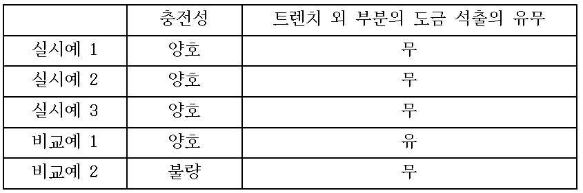
표 1에 나타내는 바와 같이, 비교예 1∼2와 달리, 실시예 1∼실시예 3에서는, 트렌치 외의 표면에 도금이 석출되지 않으며, 트렌치에 금속층이 양호하게 충전되는 것이 확인되었다.As shown in Table 1, in Examples 1 to 3, unlike Comparative Examples 1 and 2, no plating was deposited on the surfaces other than the trenches, and it was confirmed that the metal layer was well filled in the trenches.
이상으로, 실시예 1∼실시예 3의 방법에 의해, 트렌치 외의 표면에 있어서, 도금의 이상석출의 발생을 확실하게 방지할 수 있는 것을 알았다.As described above, it was found that the occurrence of abnormal precipitation of the plating on the surfaces other than the trench can be reliably prevented by the methods of Examples 1 to 3.
[산업상 이용 가능성][Industrial applicability]
이상 설명한 바와 같이, 본 발명은, 도금처리를 행하는 배선기판의 제조방법 및 그 방법에 의해 제조된 배선기판에 적합하다.INDUSTRIAL APPLICABILITY As described above, the present invention is suitable for a method of manufacturing a wiring board for performing a plating process and a wiring board manufactured by the method.
1 : 프린트 배선기판 2 : 제 1 수지층
3 : 도체회로 4 : 제 2 수지층
4a : 제 2 수지층의 표면 5 : 비아홀
6 : 트렌치 7 : 금속층
8 : 보호층 9 : 관통공
10, 40 : 무전해 도금장치 11 : 도금조
12 : 도금액 공급수단 13 : 산기수단
14 : 오버플로우조 18 : 온도조절수단
20 : 도금액 23 : 배출로
24 : 배출구 30 : 피처리기판
41 : 정류수단 42 : 지지부재1: printed wiring board 2: first resin layer
3: conductor circuit 4: second resin layer
4a: surface of the second resin layer 5:
6: trench 7: metal layer
8: Protective layer 9: Through hole
10, 40: Electroless plating apparatus 11: Plating tank
12: plating liquid supply means 13:
14: overflow tank 18: temperature control means
20: plating liquid 23: discharge path
24: outlet 30: substrate to be processed
41: rectification means 42: support member
Claims (7)
상기 피처리기판의 하방(下方)으로 상기 무전해 도금액을 공급하는 공정과,
상기 피처리기판의 하방에 공급된 상기 무전해 도금액 내로 산소함유기체를 확산시키는 공정과,
상기 무전해 도금액을 상기 피처리기판의 상방(上方)으로부터 오버플로우(overflow) 시키는 공정
을 적어도 구비하는 것을 특징으로 하는 배선기판의 제조방법.
무전해 도금액:적어도, 수용성 금속염과, 환원제와, 착화제를 함유함과 동시에, 하기 일반식(I) 내지 (V) 중 어느 것에 의해 나타내는 적어도 1종의 유황계 유기화합물로 이루어진 레벨러를 함유한다.
R1-(S)n-R2 (I)
R1-L1-(S)n-R2 (II)
R1-L1-(S)n-L2-R2 (III)
R1-(S)n-L3 (IV)
R1-L1-(S)n-L3 (V)
[일반식(I) 내지 (V) 중, n은, 1 이상의 정수,
R1, R2는, 각각 독립적으로 탄소원자, 산소원자, 인(phosphorus)원자, 유황원자, 질소원자를, 각각 임의의 수로 포함하는 지방족 환상기(環狀基) 또는 방향족 환상기, 또는 이 환상기에 임의의 1종류 이상의 치환기가 하나 이상 결합한 환상기,
L1, L2는, 각각 독립적으로 직쇄 또는 분기된 알킬쇄(alkyl chain), 알킬아미노쇄(alkylamino chain), 알킬렌쇄(alkylene chain), 알콕시쇄(alkoxy chain)로 이루어진 군 중 어느 하나이며,
L3은, 알킬기(alkyl group), 알킬렌기(alkylene group), 아미노기(amino group), 알킬아미노기(alkylamino group), 알킬렌아미노기(alkyleneamino group), 하이드록시기(hydroxyl group), 알킬하이드록시기(alkylhydroxyl group), 알킬렌하이드록시기(alkylenehydroxyl group), 카르복시기(carboxy group), 알킬카르복시기(alkylcarboxy group), 알킬렌카르복시기(alkylenecarboxy group), 알킬아미노카르복시기(alkylaminocarboxy group), 알킬렌아미노카르복시기(alkyleneaminocarboxy group), 니트로기(nitro group), 알킬니트로기(alkylnitro group), 니트릴기(nitrile group), 알킬니트릴기(alkylnitrile group), 아마이드기(amide group), 알킬아마이드기(alkylamide group), 카르보닐기(carbonyl group), 알킬카르보닐기(alkylcarbonyl group), 술폰산기(sulfonic acid group), 알킬술폰산기(alkylsulfonic acid group), 포스폰산기(phosphonic acid group), 알킬포스폰산기(alkylphosphonic acid group), 술파닐일기(sulfanilyl group), 술피닐기(sulfinyl group), 티오카르보닐기(thiocarbonyl group)로 이루어진 군 중 어느 하나이다.]A substrate to be processed having at least one of a via hole and a trench formed thereon is immersed in the electroless plating solution described below and electroless plating is performed on the substrate to be processed, A method for manufacturing a wiring board in which a plating metal is filled in at least one of a via hole and a trench,
A step of supplying the electroless plating liquid downward (below) the substrate to be processed,
Diffusing the oxygen-containing gas into the electroless plating liquid supplied to the lower side of the substrate to be processed;
A step of overflowing the electroless plating liquid from the upper side of the substrate to be processed
At least a part of the wiring board is formed.
An electroless plating solution contains at least a water-soluble metal salt, a reducing agent, and a complexing agent and a leveler comprising at least one sulfur-based organic compound represented by any one of the following general formulas (I) to (V) .
R 1 - (S) n -R 2 (I)
R 1 -L 1 - (S) n -R 2 (II)
R 1 -L 1 - (S) n -L 2 -R 2 (III)
R 1 - (S) n -L 3 (IV)
R 1 -L 1 - (S) n -L 3 (V)
[In the general formulas (I) to (V), n is an integer of 1 or more,
R 1 and R 2 each independently represent an aliphatic cyclic group or an aromatic cyclic group each containing a carbon atom, an oxygen atom, a phosphorus atom, a sulfur atom and a nitrogen atom in an arbitrary number, A cyclic group in which at least one arbitrary substituent group is bonded to the cyclic group,
L 1 and L 2 are each independently any one selected from the group consisting of a linear or branched alkyl chain, an alkylamino chain, an alkylene chain, and an alkoxy chain,
L 3 represents an alkyl group, an alkylene group, an amino group, an alkylamino group, an alkyleneamino group, a hydroxyl group, an alkylhydroxy group, an alkyleneoxy group, an alkylhydroxyl group, an alkylenehydroxyl group, a carboxy group, an alkylcarboxy group, an alkylenecarboxy group, an alkylaminocarboxy group, an alkyleneaminocarboxy group, a nitro group, an alkylnitro group, a nitrile group, an alkylnitrile group, an amide group, an alkylamide group, a carbonyl group (e.g., carbonyl group, an alkylcarbonyl group, a sulfonic acid group, an alkylsulfonic acid group, a phosphonic acid group, an alkylphosphonic acid group a sulfinyl group, a sulfinyl group, and a thiocarbonyl group.
상기 산소함유기체의 기포지름이 5∼50㎛인 것을 특징으로 하는 배선기판의 제조방법.The method according to claim 1,
Wherein the oxygen-containing gas has a bubble diameter of 5 to 50 占 퐉.
상기 무전해 도금을 개시하기 전에, 소정 시간, 상기 산소함유기체를 확산시키는 공정을 행하지 않는 것을 특징으로 하는 배선기판의 제조방법.The method according to claim 1 or 2,
Wherein the step of diffusing the oxygen-containing gas is not performed for a predetermined time before starting the electroless plating.
상기 무전해 도금은, 상기 무전해 도금액이 충전된 도금조(plating tank)와, 상기 피처리기판의 하방으로 상기 무전해 도금액을 공급하는 도금액 공급수단과, 상기 무전해 도금액 내로 산소함유기체를 확산시키는 산기수단(air diffuser)과, 상기 무전해 도금액을 상기 피처리기판의 상방으로부터 오버플로우 시키는 오버플로우조(overflow tank)를 적어도 구비하는 무전해 도금장치에 의해 이루어지는 것을 특징으로 하는 배선기판의 제조방법.The method according to any one of claims 1 to 3,
The electroless plating includes a plating tank filled with the electroless plating liquid, a plating liquid supply means for supplying the electroless plating liquid downward of the substrate to be processed, and an oxygen-containing gas diffusion And an overflow tank for overflowing the electroless plating liquid from the upper side of the substrate to be processed. The electroless plating apparatus according to claim 1, Way.
상기 산기수단이 다공성 세라믹재료에 의해 형성되는 것을 특징으로 하는 배선기판의 제조방법.The method of claim 4,
Wherein the diffusion means is formed of a porous ceramic material.
상기 무전해 도금장치가, 상기 도금조 내 상기 무전해 도금액의 흐름을 조정하는 정류수단을 구비하는 것을 특징으로 하는 배선기판의 제조방법.The method according to claim 4 or 5,
Wherein the electroless plating apparatus further comprises rectifying means for adjusting the flow of the electroless plating liquid in the plating tank.
Applications Claiming Priority (3)
| Application Number | Priority Date | Filing Date | Title |
|---|---|---|---|
| JP2014188896A JP5997741B2 (en) | 2014-09-17 | 2014-09-17 | Wiring board manufacturing method and wiring board manufactured by the method |
| JPJP-P-2014-188896 | 2014-09-17 | ||
| PCT/JP2015/004679 WO2016042754A1 (en) | 2014-09-17 | 2015-09-14 | Method for manufacturing wiring substrate and wiring substrate manufactured thereby |
Publications (2)
| Publication Number | Publication Date |
|---|---|
| KR20170056535A true KR20170056535A (en) | 2017-05-23 |
| KR102291601B1 KR102291601B1 (en) | 2021-08-23 |
Family
ID=55532810
Family Applications (1)
| Application Number | Title | Priority Date | Filing Date |
|---|---|---|---|
| KR1020177006566A KR102291601B1 (en) | 2014-09-17 | 2015-09-14 | Method for manufacturing wiring substrate and wiring substrate manufactured thereby |
Country Status (6)
| Country | Link |
|---|---|
| US (1) | US20170253975A1 (en) |
| EP (1) | EP3196339B1 (en) |
| JP (1) | JP5997741B2 (en) |
| KR (1) | KR102291601B1 (en) |
| CN (1) | CN106661734B (en) |
| WO (1) | WO2016042754A1 (en) |
Families Citing this family (5)
| Publication number | Priority date | Publication date | Assignee | Title |
|---|---|---|---|---|
| JP6914073B2 (en) * | 2017-03-28 | 2021-08-04 | 上村工業株式会社 | Surface treatment equipment |
| CN107326348A (en) * | 2017-07-24 | 2017-11-07 | 电子科技大学 | A kind of method and related chemistry copper plating bath that core inductance quality value is lifted based on chemical plating Porous Cu |
| KR102421980B1 (en) * | 2017-07-26 | 2022-07-18 | 삼성전기주식회사 | Printed circuit board |
| CN109972180B (en) * | 2019-04-12 | 2020-12-18 | 博敏电子股份有限公司 | New use of 2, 2' -dithiodipyridine, electroplating hole-filling additive using the same and electroplating method using the additive |
| CN114786366B (en) * | 2022-06-22 | 2022-09-02 | 四川英创力电子科技股份有限公司 | Floating type chemical plating device and method for driving bubbles in holes of circuit board |
Citations (3)
| Publication number | Priority date | Publication date | Assignee | Title |
|---|---|---|---|---|
| JPH1072678A (en) * | 1996-08-29 | 1998-03-17 | Nec Toyama Ltd | Electroless plating device and plating method |
| JP2010031361A (en) * | 2008-07-01 | 2010-02-12 | C Uyemura & Co Ltd | Electroless plating solution, electroless plating method using the same, and method for production of wiring board |
| JP2011173063A (en) * | 2010-02-24 | 2011-09-08 | Kyocera Corp | Bubble generation member, bubble generation apparatus using the same, and bubble generation method |
Family Cites Families (6)
| Publication number | Priority date | Publication date | Assignee | Title |
|---|---|---|---|---|
| US4525390A (en) * | 1984-03-09 | 1985-06-25 | International Business Machines Corporation | Deposition of copper from electroless plating compositions |
| US4684545A (en) * | 1986-02-10 | 1987-08-04 | International Business Machines Corporation | Electroless plating with bi-level control of dissolved oxygen |
| JPS63312983A (en) * | 1987-06-16 | 1988-12-21 | Hitachi Ltd | Electroless copper plating method and equipment therefor |
| JP3091583B2 (en) * | 1992-09-14 | 2000-09-25 | 株式会社ジャパンエナジー | Method and apparatus for supplying oxygen to electroless plating solution |
| TWI485286B (en) * | 2011-11-16 | 2015-05-21 | Ebara Corp | Electroless plating and electroless plating |
| JP6068123B2 (en) * | 2012-12-14 | 2017-01-25 | 上村工業株式会社 | Printed wiring board manufacturing method and printed wiring board manufactured by the method |
-
2014
- 2014-09-17 JP JP2014188896A patent/JP5997741B2/en active Active
-
2015
- 2015-09-14 WO PCT/JP2015/004679 patent/WO2016042754A1/en active Application Filing
- 2015-09-14 KR KR1020177006566A patent/KR102291601B1/en active IP Right Grant
- 2015-09-14 EP EP15842761.7A patent/EP3196339B1/en active Active
- 2015-09-14 CN CN201580047825.1A patent/CN106661734B/en active Active
- 2015-09-14 US US15/511,063 patent/US20170253975A1/en not_active Abandoned
Patent Citations (3)
| Publication number | Priority date | Publication date | Assignee | Title |
|---|---|---|---|---|
| JPH1072678A (en) * | 1996-08-29 | 1998-03-17 | Nec Toyama Ltd | Electroless plating device and plating method |
| JP2010031361A (en) * | 2008-07-01 | 2010-02-12 | C Uyemura & Co Ltd | Electroless plating solution, electroless plating method using the same, and method for production of wiring board |
| JP2011173063A (en) * | 2010-02-24 | 2011-09-08 | Kyocera Corp | Bubble generation member, bubble generation apparatus using the same, and bubble generation method |
Also Published As
| Publication number | Publication date |
|---|---|
| CN106661734B (en) | 2022-02-25 |
| WO2016042754A1 (en) | 2016-03-24 |
| JP5997741B2 (en) | 2016-09-28 |
| EP3196339B1 (en) | 2019-08-28 |
| KR102291601B1 (en) | 2021-08-23 |
| JP2016060935A (en) | 2016-04-25 |
| CN106661734A (en) | 2017-05-10 |
| EP3196339A1 (en) | 2017-07-26 |
| EP3196339A4 (en) | 2017-11-29 |
| US20170253975A1 (en) | 2017-09-07 |
Similar Documents
| Publication | Publication Date | Title |
|---|---|---|
| CN108342718B (en) | Electroless copper plating composition | |
| KR101234599B1 (en) | Electroless Gold Plating Bath and Method | |
| KR101590031B1 (en) | Electroless plating solution method for electroless plating using the same and method for manufacturing circuit board | |
| KR102291601B1 (en) | Method for manufacturing wiring substrate and wiring substrate manufactured thereby | |
| JP2011249511A (en) | Method of manufacturing substrate with gold-plating metal fine pattern, substrate with gold-plating metal fine pattern, printed wiring board, interposer, and semiconductor device | |
| US20210047734A1 (en) | Pretreating liquid for electroless plating to be used during reduction treatment, and process for producing printed wiring board | |
| KR102440121B1 (en) | Method for manufacturing a printed wiring board | |
| KR20150095669A (en) | Production method for printed wiring board and printed wiring board produced by said method | |
| US20160145745A1 (en) | Formaldehyde-free electroless metal plating compositions and methods | |
| EP3257967B1 (en) | Pretreatment agent for electroless plating, and pretreatment method and manufacturing method for printed wiring board in which pretreatment agent for electroless plating is used | |
| KR102375734B1 (en) | Aqueous alkaline pretreatment solution for use prior to deposition of palladium activation layer, method and use thereof | |
| KR20230163447A (en) | Plasma-treatment method of substrate surface | |
| JP5490942B2 (en) | Surface treatment method for forming printed wiring board and etching treatment liquid used in the surface treatment method |
Legal Events
| Date | Code | Title | Description |
|---|---|---|---|
| E902 | Notification of reason for refusal | ||
| E701 | Decision to grant or registration of patent right |