KR20170017841A - A magnetic sensor and an integratred circuit - Google Patents
A magnetic sensor and an integratred circuit Download PDFInfo
- Publication number
- KR20170017841A KR20170017841A KR1020160100329A KR20160100329A KR20170017841A KR 20170017841 A KR20170017841 A KR 20170017841A KR 1020160100329 A KR1020160100329 A KR 1020160100329A KR 20160100329 A KR20160100329 A KR 20160100329A KR 20170017841 A KR20170017841 A KR 20170017841A
- Authority
- KR
- South Korea
- Prior art keywords
- signal
- chopper
- magnetic
- magnetic field
- detection signal
- Prior art date
- Legal status (The legal status is an assumption and is not a legal conclusion. Google has not performed a legal analysis and makes no representation as to the accuracy of the status listed.)
- Withdrawn
Links
Images


Classifications
-
- G—PHYSICS
- G01—MEASURING; TESTING
- G01R—MEASURING ELECTRIC VARIABLES; MEASURING MAGNETIC VARIABLES
- G01R33/00—Arrangements or instruments for measuring magnetic variables
- G01R33/0023—Electronic aspects, e.g. circuits for stimulation, evaluation, control; Treating the measured signals; calibration
-
- H—ELECTRICITY
- H02—GENERATION; CONVERSION OR DISTRIBUTION OF ELECTRIC POWER
- H02P—CONTROL OR REGULATION OF ELECTRIC MOTORS, ELECTRIC GENERATORS OR DYNAMO-ELECTRIC CONVERTERS; CONTROLLING TRANSFORMERS, REACTORS OR CHOKE COILS
- H02P6/00—Arrangements for controlling synchronous motors or other dynamo-electric motors using electronic commutation dependent on the rotor position; Electronic commutators therefor
- H02P6/14—Electronic commutators
- H02P6/16—Circuit arrangements for detecting position
-
- G—PHYSICS
- G01—MEASURING; TESTING
- G01R—MEASURING ELECTRIC VARIABLES; MEASURING MAGNETIC VARIABLES
- G01R23/00—Arrangements for measuring frequencies; Arrangements for analysing frequency spectra
- G01R23/16—Spectrum analysis; Fourier analysis
- G01R23/165—Spectrum analysis; Fourier analysis using filters
-
- G—PHYSICS
- G01—MEASURING; TESTING
- G01R—MEASURING ELECTRIC VARIABLES; MEASURING MAGNETIC VARIABLES
- G01R33/00—Arrangements or instruments for measuring magnetic variables
- G01R33/0023—Electronic aspects, e.g. circuits for stimulation, evaluation, control; Treating the measured signals; calibration
- G01R33/0029—Treating the measured signals, e.g. removing offset or noise
-
- G—PHYSICS
- G01—MEASURING; TESTING
- G01R—MEASURING ELECTRIC VARIABLES; MEASURING MAGNETIC VARIABLES
- G01R33/00—Arrangements or instruments for measuring magnetic variables
- G01R33/0088—Arrangements or instruments for measuring magnetic variables use of bistable or switching devices, e.g. Reed-switches
-
- G—PHYSICS
- G01—MEASURING; TESTING
- G01R—MEASURING ELECTRIC VARIABLES; MEASURING MAGNETIC VARIABLES
- G01R33/00—Arrangements or instruments for measuring magnetic variables
- G01R33/02—Measuring direction or magnitude of magnetic fields or magnetic flux
-
- G—PHYSICS
- G01—MEASURING; TESTING
- G01R—MEASURING ELECTRIC VARIABLES; MEASURING MAGNETIC VARIABLES
- G01R33/00—Arrangements or instruments for measuring magnetic variables
- G01R33/02—Measuring direction or magnitude of magnetic fields or magnetic flux
- G01R33/06—Measuring direction or magnitude of magnetic fields or magnetic flux using galvano-magnetic devices
- G01R33/07—Hall effect devices
-
- H—ELECTRICITY
- H02—GENERATION; CONVERSION OR DISTRIBUTION OF ELECTRIC POWER
- H02K—DYNAMO-ELECTRIC MACHINES
- H02K11/00—Structural association of dynamo-electric machines with electric components or with devices for shielding, monitoring or protection
- H02K11/20—Structural association of dynamo-electric machines with electric components or with devices for shielding, monitoring or protection for measuring, monitoring, testing, protecting or switching
-
- H—ELECTRICITY
- H02—GENERATION; CONVERSION OR DISTRIBUTION OF ELECTRIC POWER
- H02K—DYNAMO-ELECTRIC MACHINES
- H02K11/00—Structural association of dynamo-electric machines with electric components or with devices for shielding, monitoring or protection
- H02K11/30—Structural association with control circuits or drive circuits
Landscapes
- Physics & Mathematics (AREA)
- General Physics & Mathematics (AREA)
- Condensed Matter Physics & Semiconductors (AREA)
- Engineering & Computer Science (AREA)
- Power Engineering (AREA)
- Microelectronics & Electronic Packaging (AREA)
- Mathematical Physics (AREA)
- Measuring Magnetic Variables (AREA)
Abstract
Description
본 발명은 회로 기술 분야에 관한 것이다. 특히, 본 발명은 자기 센서에 관한 것이다. 본 발명은 또한 영구 자석 회전자에 대한 드라이버에 관한 것이다.The present invention relates to the field of circuit technology. More particularly, the present invention relates to a magnetic sensor. The present invention also relates to a driver for a permanent magnet rotor.
자기 센서는 현대의 산업 및 전자 제품에 널리 응용되어, 전류, 위치 및 방향과 같은 물리적 파라미터를 측정하기 위하여 자계 강도를 유도한다. 모터는 자기 센서의 주요 응용 분야이다. 자기 센서는 모터 내의 회전자 자극 위치 센서의 역할을 할 수 있다.Magnetic sensors are widely applied in modern industrial and electronic products to derive magnetic field strengths to measure physical parameters such as current, position and orientation. Motors are a major application of magnetic sensors. The magnetic sensor can serve as a rotor pole position sensor in the motor.
일반적으로, 자기 센서는 자계 검출 신호를 출력만 할 수 있다. 그러나, 자계 검출 신호는 약하고 자기 센서의 오프셋과 혼합되어, 정확한 자계 검출 신호를 얻기가 힘들다.Generally, the magnetic sensor can only output a magnetic field detection signal. However, the magnetic field detection signal is weak and mixed with the offset of the magnetic sensor, so that it is difficult to obtain an accurate magnetic field detection signal.
본 발명은 자기 센서 및 그의 응용을 제공한다. 본 발명의 실시예에 따르면, 자기 센서는 외부 전원에 연결되는 입력 포트; 자기 검출 신호를 생성하도록 구성되는 자계 검출 회로; 자기 검출 신호에 응답하여 자기 센서의 동작을 제어하도록 구성된 출력 제어 회로; 및 출력 포트를 포함하되, 상기 자계 검출 회로는: 외부 자계를 검출하고 검출 신호를 출력하도록 구성되는 자기 감지 소자, 상기 검출 신호를 증폭하고 상기 검출 신호로부터의 간섭을 제거하여 처리된 검출 신호를 생성하도록 구성되는 신호 처리 소자, 및 처리된 검출 신호를 자기 검출 신호로 변환하도록 구성되며, 상기 자기 센서를 적어도 상기 자기 검출 신호에 응답하여 제1 상태 및 제2 상태 중 적어도 하나에서 동작하도록 제어하는데 이용되는 변환 소자를 포함하되, 제1 상태에서, 부하 전류는 출력 포트로부터 자기 센서의 외부로 흐르고, 또한 제2 상태에서, 부하 전류는 상기 자기 센서의 외부로부터 출력 포트로 흐르며, 상기 신호 처리 소자는 증폭기 및 필터 회로를 포함하며, 상기 증폭기의 이득은 상기 필터 회로의 이득보다 더 크다.The present invention provides a magnetic sensor and its application. According to an embodiment of the present invention, a magnetic sensor includes an input port connected to an external power source; A magnetic field detection circuit configured to generate a magnetic detection signal; An output control circuit configured to control an operation of the magnetic sensor in response to the magnetic detection signal; And an output port, wherein the magnetic field detection circuit comprises: a magnetic sensing element configured to detect an external magnetic field and output a detection signal; amplify the detection signal and remove interference from the detection signal to generate a processed detection signal And to control the magnetic sensor to operate in at least one of a first state and a second state in response to at least the magnetic detection signal, the signal processing element being configured to convert the processed detection signal into a magnetic detection signal, Wherein in the first state the load current flows from the output port to the outside of the magnetic sensor and in the second state the load current flows from the outside of the magnetic sensor to the output port, An amplifier and a filter circuit, wherein the gain of the amplifier is greater than the gain of the filter circuit.
일부 실시예에서, 상기 검출 신호는 자계 신호 및 편차 신호를 포함하며, 상기 증폭기는 초퍼 증폭기이며, 또한 상기 필터 회로는 저역 필터이고, 상기 신호 처리 소자는: 상기 검출 신호를 각각 초퍼 주파수 및 베이스밴드 주파수에 대응하는 상기 편차 신호 및 상기 자계 신호로 분리하도록 구성되는 제1 초퍼 스위치를 포함하고, 상기 초퍼 증폭기는 상기 편차 신호 및 상기 자계 신호를 증폭하고, 증폭된 편차 신호 및 증폭된 자계 신호를 각각 초퍼 주파수 및 베이스밴드 주파수 상으로 스위칭하도록 구성되고, 또한 상기 필터 회로는 상기 초퍼 주파수에서 상기 편차 신호를 필터링아웃 하도록 구성된다.In some embodiments, the detection signal comprises a magnetic field signal and a deviation signal, the amplifier is a chopper amplifier, and the filter circuit is a low pass filter, the signal processing device comprising: Wherein the chopper amplifier amplifies the deviation signal and the magnetic field signal, and outputs the amplified deviation signal and the amplified magnetic field signal to the first and second chopper amplifiers Chopper frequency and baseband frequency, and the filter circuit is further configured to filter out the deviation signal at the chopper frequency.
일부 실시예에서, 상기 초퍼 증폭기는 제1 증폭기; 및 제2 초퍼 스위치를 포함하되, 상기 제1 증폭기는 상기 제1 초퍼 스위치로부터의 상기 편차 신호 및 상기 증폭 신호에 대해 제1 단계 증폭을 수행하여 각각 상기 증폭된 편차 신호 및 상기 증폭된 자계 신호를 생성하도록 구성되며, 또한 상기 제2 초퍼 스위치는 상기 증폭된 편차 신호 및 증폭된 자계 신호를 초퍼 주파수 및 베이스밴드 주파수 상으로 스위칭하도록 구성된다.In some embodiments, the chopper amplifier comprises a first amplifier; And a second chopper switch, wherein the first amplifier performs a first stage amplification on the deviation signal and the amplification signal from the first chopper switch to generate the amplified deviation signal and the amplified magnetic field signal, respectively, And the second chopper switch is configured to switch the amplified deviation signal and the amplified magnetic field signal onto the chopper frequency and the baseband frequency.
일부 실시예에서, 상기 초퍼 주파수는 100 K Hertz 보다 크거나 및/또는 상기 베이스밴드 주파수는 200 Hertz 보다 적다.In some embodiments, the chopper frequency is greater than 100 K Hertz and / or the baseband frequency is less than 200 Hertz.
일부 실시예에서, 상기 초퍼 증폭기는 상기 제2 초퍼 스위치와 상기 필터 회로 사이에 배치된 제2 증폭기를 더 포함하며, 상기 제2 증폭기는 상기 초퍼 주파수 상으로 스위칭되는 증폭된 편차 신호 및 상기 베이스밴드 주파수 상으로 스위칭되는 증폭된 자계 신호에 대해 제2 단계 증폭을 수행하도록 구성된다.In some embodiments, the chopper amplifier further comprises a second amplifier disposed between the second chopper switch and the filter circuit, the second amplifier having an amplified deviation signal switched on the chopper frequency, Stage amplification for the amplified magnetic field signal that is switched on the frequency.
일부 실시예에서, 상기 제1 증폭기의 이득은 상기 제2 증폭기의 이득보다 크다.In some embodiments, the gain of the first amplifier is greater than the gain of the second amplifier.
일부 실시예에서, 상기 신호 처리 소자는 상기 초퍼 증폭기와 상기 필터 회로 사이에 결합된 샘플 앤 홀드 회로를 더 포함하며, 상기 샘플 앤드 홀드 회로는 각각 제1 클록 반주기 및 제2 클록 반주기 동안 제1 쌍의 차동 신호를 샘플링하고, 클록 주기 동안 두 쌍의 샘플링된 차동 신호를 출력하도록 구성된다.In some embodiments, the signal processing element further comprises a sample and hold circuit coupled between the chopper amplifier and the filter circuit, wherein the sample and hold circuit comprises a first clock half-period and a second half period during a second clock half- And to output two pairs of sampled differential signals during the clock period.
일부 실시예에서, 상기 필터 회로는 두 쌍의 샘플링된 차동 신호를 기초로 제2 쌍의 차동 신호를 연산하도록 구성되는 제1 필터를 더 포함한다.In some embodiments, the filter circuit further comprises a first filter configured to compute a second pair of differential signals based on the two pairs of sampled differential signals.
일부 실시예에서, 상기 필터 회로는 제2 쌍의 차동 신호를 더욱 증폭하고, 편차 신호를 제거하고, 제3 쌍의 차동 신호를 생성하도록 구성되는 제2 필터를 더 포함한다.In some embodiments, the filter circuit further comprises a second filter configured to further amplify the second pair of differential signals, remove the deviation signal, and generate a third pair of differential signals.
일부 실시예에서, 상기 제1 필터의 이득은 상기 제2 필터의 이득보다 적다.In some embodiments, the gain of the first filter is less than the gain of the second filter.
일부 실시예에서, 자기 센서는 자기 검출 신호를 기초로 제1 상태 및 제2 상태 중 적어도 하나에서 동작하도록 상기 자기 센서를 제어하도록 구성되는 출력 제어 회로를 더 포함하며, 상기 출력 제어 회로는 제1 상태에서 부하 전류가 출력 포트로부터 자기 센서의 외부로 흐르도록 하는 제1 전류 경로를 형성하도록 출력 포트와 결합된 제1 스위치; 및 제2 상태에서 부하 전류가 자기 센서의 외부로부터 출력 포트로 흐르도록 허용하는 제2 전류 경로를 형성하도록 출력 포트와 결합되는 제2 스위치를 포함하며, 제1 스위치 및 제2 스위치는 제1 및 제2 전류 경로를 선택적으로 턴 온하도록 자기 검출 신호를 기초로 동작한다.In some embodiments, the magnetic sensor further comprises an output control circuit configured to control the magnetic sensor to operate in at least one of a first state and a second state based on the magnetic detection signal, A first switch coupled to the output port to form a first current path that causes the load current to flow from the output port to the outside of the magnetic sensor; And a second switch coupled to the output port to form a second current path that allows the load current to flow from the exterior of the magnetic sensor to the output port in a second state, And operates based on the magnetic detection signal to selectively turn on the second current path.
일부 실시예에서, 외부 전원은 교류(AC) 전원이며, 자기 검출 신호는 스위치 검출 신호이며, 자기 검출 신호의 스위칭 주파수는 AC 전원의 주파수에 비례하거나 또는 AC 전원의 주파수의 2배이다.In some embodiments, the external power source is an alternating current (AC) power source, the magnetic detection signal is a switch detection signal, and the switching frequency of the magnetic detection signal is proportional to the frequency of the AC power source or twice the frequency of the AC power source.
본 발명의 다른 실시예에 따르면, 자기 센서용 집적 회로로서: 외부 전원에 연결되는 입력 포트; 출력 포트; 및 자기 검출 신호를 생성하도록 구성되며, 외부 자계를 검출하고 검출 신호를 출력하도록 구성되는 자기 감지 소자 - 상기 검출 신호는 자계 신호 및 편차 신호를 포함함 - , 상기 검출 신호를 증폭하고 상기 검출 신호로부터의 간섭을 제거하여 처리된 검출 신호를 생성하도록 구성되는 신호 처리 소자, 및 처리된 검출 신호를 자기 검출 신호로 변환하도록 구성되며, 상기 자기 센서를 적어도 상기 자기 검출 신호에 응답하여 제1 상태 및 제2 상태 중 적어도 하나에서 동작하도록 제어하는데 이용되는 변환 소자를 포함하되, 상기 신호 처리 소자는 상기 검출 신호를 각각 초퍼 주파수 및 베이스밴드 주파수에 대응하는 상기 자계 신호 및 상기 편차 신호로 분리하도록 구성되는 제1 초퍼 스위치; 상기 자계 신호 및 상기 편차 신호를 개별적으로 증폭하고 증폭된 편차 신호 및 증폭된 자계 신호를 각각 초퍼 주파수 및 베이스밴드 주파수 상으로 스위칭하도록 구성된 초퍼 증폭기, 및 상기 초퍼 주파수로 스위칭된 상기 편차 신호를 제거하도록 구성되는 필터 회로를 포함하되, 상기 초퍼 증폭기의 이득은 상기 필터 회로의 이득보다 더 크다.According to another embodiment of the present invention, there is provided an integrated circuit for a magnetic sensor, comprising: an input port connected to an external power source; Output port; And a magnetic sensing element configured to generate a magnetic detection signal, the magnetic sensing element being configured to detect an external magnetic field and output a detection signal, the detection signal comprising a magnetic field signal and a deviation signal; And to convert the processed detection signal into a magnetic detection signal, wherein the magnetic detection sensor is configured to convert the processed detection signal into a first detection signal and a second detection signal in response to at least the magnetic detection signal, 2 state, wherein the signal processing element is configured to separate the detection signal into the magnetic field signal and the deviation signal corresponding to the chopper frequency and the baseband frequency, respectively, 1 chopper switch; A chopper amplifier configured to amplify the magnetic field signal and the deviation signal separately and to switch the amplified deviation signal and the amplified magnetic field signal on chopper frequency and baseband frequency, respectively, and to remove the deviation signal switched to the chopper frequency Wherein the gain of the chopper amplifier is greater than the gain of the filter circuit.
본 발명의 다른 실시예에 따르면, 모터 어셈블리는 교류(AC) 전력을 모터에 제공하는 외부 전원에 결합된 모터, 모터에 의해 생성된 자계를 검출하도록 구성된 자기 센서, 및 검출된 자계를 기초로 결정된 자기 센서의 동작 상태를 기초로 모터를 제어하도록 구성된 양방향 스위치를 포함하며, 상기 자기 센서는 자계를 검출하고 검출된 자계를 기초로 자기 검출 신호를 생성하도록 구성되며, 외부 자계를 검출하고 검출 신호를 출력하도록 구성된 자기 감지 소자, 검출 신호를 증폭하고 검출 신호로부터 간섭을 제거하여 처리된 검출 신호를 생성하도록 구성된 신호 처리 소자, 및 처리된 검출 신호를 자기 검출 신호로 변환하도록 구성되며, 상기 자기 센서를 적어도 상기 자기 검출 신호에 응답하여 제1 상태 및 제2 상태 중 적어도 하나에서 동작하도록 제어하는데 이용되는 변환 소자를 포함하는 자계 검출 회로; 및 자기 검출 신호를 기초로 적어도 자기 검출 신호에 응답하는 제1 상태 및 ㅈ2 상태 중 적어도 하나에서 동작하도록 자기 센서를 제어하도록 구성되는 출력 제어 회로를 포함하며, 제1 상태에서, 전류는 자기 센서의 외부로부터 자기 센서로 흐르고, 제2 상태에서, 전류는 자기 센서로부터 자기 센서의 외부로 흐르며, 상기 신호 처리 소자는 증폭기 및 필터 회로를 포함하며, 증폭기의 이득은 필터 회로의 이득 보다 크다.According to another embodiment of the invention, the motor assembly comprises a motor coupled to an external power source providing AC power to the motor, a magnetic sensor configured to detect a magnetic field generated by the motor, And a bi-directional switch configured to control the motor based on an operation state of the magnetic sensor, wherein the magnetic sensor is configured to detect a magnetic field and generate a magnetic detection signal based on the detected magnetic field, A signal processing element configured to amplify the detection signal and remove the interference from the detection signal to generate a processed detection signal, and to convert the processed detection signal into a magnetic detection signal, And to operate in at least one of the first state and the second state in response to at least the magnetic detection signal. A magnetic field detection circuit including a conversion element used for programming; And an output control circuit configured to control the magnetic sensor to operate in at least one of a first state and a second state responsive to at least a magnetic detection signal based on the magnetic detection signal, And in the second state, the current flows from the magnetic sensor to the outside of the magnetic sensor, and the signal processing element includes an amplifier and a filter circuit, and the gain of the amplifier is larger than the gain of the filter circuit.
본 명세서에 설명된 방법, 시스템, 및/또는 프로그래밍은 예시적 실시예 측면에서 더욱 설명된다. 이들 실시예는 도면을 참조로 상세히 설명된다. 이들 실시예는 비제한적 실시예로서, 여기서 도면 번호는 도면에 걸쳐 유사한 구조를 나타낸다.
도 1은 본 공개의 일 실시예에 따른 자기 센서의 예시적인 개략도이다.
도 2은 본 공개의 일 실시예에 따른 상기 신호 처리 소자(1110)의 예시적인 개략도이다.
도 3a는 본 공개의 일 실시예에 따른 초퍼 증폭기(1204)의 예시적인 개략도이다.
도 3b는 본 공개의 일 실시예에 따른 초퍼 증폭기(1204)의 다른 개략도이다.
도 4는 본 공개의 일 실시예에 따른 자기 센서의 예시적인 개략도이다.
도 5는 본 공개의 일 실시예에 따른 정류기 회로(1402)의 예시적인 개략도이다.
도 6은 본 공개의 일 실시예에 따른 홀 검출기(1420) 및 제 1 초퍼 스위치의 예시적인 회로도이다.
도 7은 도 6의 회로도에 따른 예시적인 신호 출력을 도시한다.
도 8은 본 공개의 일 실시예에 따른 필터 회로(1428)의 예시적인 회로도이다.
도 9는 본 공개의 일 실시예에 따른 비교기 회로(1430)의 예시적인 회로도이다.
도 10는 자계의 극성을 결정하기 위한 예시적인 개략도이다.
도 11은 클록 주기의 예시적인 신호 출력을 도시한다.
도 12는 본 공개의 일 실시예에 따른 출력 제어 회로(1406)의 예시적인 회로도이다.
도 13은 본 공개의 다른 실시예에 따른 출력 제어 회로의 예시적인 회로도이다.
도 14는 본 공개의 또 다른 실시예에 따른 출력 제어 회로의 예시적인 회로도이다.
도 15는 본 공개에 따라 구성되는 자기 센서를 통합하는 모터(2500)의 예시적인 개략도이다.
도 16은 본 공개에 따라 구성되는 자기 센서를 통합하는 동기식 모터(2600)의 예시적인 개략도이다.The methods, systems, and / or programming described herein are further described in terms of exemplary embodiments. These embodiments are described in detail with reference to the drawings. These embodiments are non-limiting examples in which reference numerals indicate like structures throughout the drawings.
1 is an exemplary schematic diagram of a magnetic sensor in accordance with an embodiment of the present disclosure;
2 is an exemplary schematic diagram of the
3A is an exemplary schematic diagram of a
3B is another schematic diagram of a
4 is an exemplary schematic diagram of a magnetic sensor in accordance with one embodiment of the present disclosure;
5 is an exemplary schematic diagram of a
6 is an exemplary circuit diagram of a
FIG. 7 illustrates an exemplary signal output according to the circuit diagram of FIG.
8 is an exemplary circuit diagram of a
9 is an exemplary circuit diagram of a
10 is an exemplary schematic diagram for determining the polarity of the magnetic field.
Figure 11 shows an exemplary signal output of a clock period.
12 is an exemplary circuit diagram of an
13 is an exemplary circuit diagram of an output control circuit according to another embodiment of the present disclosure;
14 is an exemplary circuit diagram of an output control circuit according to another embodiment of the present disclosure;
15 is an exemplary schematic diagram of a
16 is an exemplary schematic diagram of a
이하의 상세한 설명에서, 수개의 특정 상세가 관련 기술이 철저한 이해를 제공하기 위하여 예로서 제시되었다. 그러나, 당업자에게는 본 발명이 그러한 상세없이도 실시될 수 있음이 명백하다. 다른 예에서, 공지된 방법, 절차, 시스템, 구성 요소 및/또는 회로가 본 발명의 측면을 불필요하게 모호하게 하는 것을 회피하기 위하여 상세 없이 상대적으로 높은 레벨에서 설명되었다.In the following detailed description, numerous specific details are set forth in order to provide a thorough understanding of the related art. However, it will be apparent to those skilled in the art that the present invention may be practiced without such details. In other instances, well-known methods, procedures, systems, components, and / or circuits have been described at a relatively high level without detail in order to avoid unnecessarily obscuring aspects of the present invention.
상세한 설명 및 청구범위를 통해, 용어가 명백하게 언급된 의미를 넘어서는 측면에서 제안되거나 암시된 미묘한 의미를 가질 수 있다. 유사하게, 여기에 이용된 용어 "일 실시예/예에서"는 반드시 동일한 실시예를 지칭할 필요는 없으며, 용어 "다른 실시예/예에서"는 반드시 상이한 실시예를 지칭할 필요가 없다. 예를 들면, 청구된 요지는 전체로서 또는 일부에서 예시적 실시예의 조합을 포함하는 것을 의도한다.Throughout the description and the claims, a term may have subtle meaning suggested or implied in terms that is beyond the explicitly stated meaning. Similarly, the term " in one embodiment / example "used herein need not necessarily refer to the same embodiment, and the term " in another embodiment / example" For example, the claimed subject matter is intended to include a combination of exemplary embodiments in whole or in part.
일반적으로, 용어들은 문맥 내의 활용으로부터 적어도 일부 이해될 수 있다. 예를 들면, 여기에 이용된 "및", "또는", 또는 "및/또는"과 같은 용어는 그러한 용어가 이용되는 문맥의 적어도 일부에 의존할 수 있는 다양한 의미를 포함할 수 있다. 일반적으로, 여기에서 이용되는 A, B, 또는 C와 같은 리스트를 관련짓기 위하여 "또는"이 이용되는 경우, 포함적 의미로 이용되는 A, B 및 C 외에도, 배타적 의미로 이용되는 A, B 또는 C를 의미할 수 있다. 또한, 여기에 이용되는 용어 "하나 이상"은 문맥의 적어도 일부에 의존하여 단일 의미에서 어떠한 특성, 구조, 또는 특징을 설명하거나 또는 복수의 의미에서의 특성, 구조 또는 특징의 조합을 설명하는데 이용될 수 있다. 유사하게, "a", "an", 또는 "the"와 같은 용어는 다시 적어도 문맥의 일부에 의존하여 단수 용법을 전달하거나 또는 복수 용법을 전달하는 것으로 이해될 수 있다. 또한, 용어 "~을 기초로(based on)"는 반드시 요인의 배타적 집합을 전하려는 의도는 아니고, 대신에, 적어도 문맥의 일부에 의존하여 다시 불필요하게 명확하게 설명되지 않은 추가적 요인의 존재를 허용할 수 있다.In general, terms may be at least partially understood from contextual use. For example, terms such as "and" or "or" and / or ", as used herein, may include various meanings that may depend on at least a part of the context in which such term is used. In general, when "or" is used to relate a list such as A, B, or C used herein, A, B, or C, which are used exclusively, in addition to A, C, respectively. Furthermore, the term "one or more ", as used herein, is to be interpreted as referring to any characteristic, structure, or characteristic in a single sense, or to describe a combination of characteristic, . Similarly, terms such as "a "," an ", or "the" may again be understood to convey singular or at least multiple uses depending at least in part on the context. It should also be understood that the term "based on" is not intended to convey an exclusive set of factors, but instead permits the presence of additional factors that are not necessarily undifferentiated again, can do.
본 공개의 자기 센서는 적어도 하나의 폴드형 캐스케이드(folded cascade) 증폭기를 사용한다. 폴드형 캐스케이드 증폭기는 큰 이득을 갖도록 매우 작은 입력 신호를 효율적으로 증폭시킬 수 있다. 또한, 폴드형 캐스케이드 증폭기는 우수한 주파수 특징을 갖고 구성되며 매우 넓은 주파수 범위로 확장되는 신호를 처리하는 것이 가능하다. 또한, 본 공개의 자기 센서는 추가 A/D 변환 장비를 요구하지 않고 시티(city) AC 전원에 직접적으로 연결될 수 있다. 그러므로, 본 공개는 다양한 분야로의 자기 센서의 구현을 용이하게 한다. 또한, 자계 검출 회로는 검출된 자계 신호를 효율적으로 증폭하고 전압을 조절하여 간섭 신호를 필터링할 수 있다. 그러므로, 자기 센서는 전기 회전자의 동작을 제어하도록 외부 자계의 극성에 관하여 더욱 정확한 신호를 생성할 수 있다.The disclosed magnetic sensor uses at least one folded cascade amplifier. A folded cascade amplifier can efficiently amplify a very small input signal to have a large gain. In addition, folded cascade amplifiers are configured with excellent frequency characteristics and are capable of processing signals that extend over a very wide frequency range. In addition, the disclosed magnetic sensor can be directly connected to a city AC power source without requiring additional A / D conversion equipment. Therefore, the present disclosure facilitates the implementation of magnetic sensors in various fields. In addition, the magnetic field detection circuit can efficiently filter the interference signal by amplifying the detected magnetic field signal and adjusting the voltage. Therefore, the magnetic sensor can generate a more accurate signal about the polarity of the external magnetic field to control the operation of the electric rotor.
추가적인 신규한 특징은, 이하의 기재에서 부분적으로 상술될 것이며 부분적으로 이하의 기재 및 동반하는 도면의 검사 이후 당업자에게 명백해질 것이며 예시의 생산 또는 동작에 의해 학습될 수 있다. 본 공개의 신규한 특징은 방법, 수단 및 이하에서 논의되는 상세한 예시에서 상술된 결합에 의한 다양한 측면의 실행 또는 사용에 의해 구현되며 얻어질 수 있다. 자기 센서, 자기 센서에서 수행되는 신호 처리 방법 및 자기 센서를 사용하는 모터 및 본 명세서에서 이하에서 개시되는 신호 처리 방법은 당업자 중 하나에게 알려져 있되, 집적 회로 및 기타 회로 구현에 한정되지 않는 임의의 회로 기술을 사용하여 성취될 수 있다.Additional novel features will be set forth in part in the description that follows, and in part will be apparent to those skilled in the art upon examination of the following description and accompanying drawings, and may be learned by way of example production or operation. The novel features of the present disclosure may be realized and obtained by means of the practice or use of the various aspects of the methods, means and combinations described above in the detailed examples discussed below. A magnetic sensor, a signal processing method performed in a magnetic sensor, and a motor using a magnetic sensor, and a signal processing method disclosed herein are known to any one of ordinary skill in the art and include any circuitry not limited to integrated circuits and other circuit implementations Technology. ≪ / RTI >
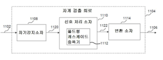
도 1는 본 공개의 일 실시예에 따른 자기 센서의 예시적인 계략도이다. 본 실시예에 따른 자기 센서는 입력 포트(1102), 자계 검출 회로(1104) 및 출력 포트(1106)를 포함한다. 입력 포트(1102)는 외부 전원에 연결되어 자계 검출 회로(1104)에 전력을 제공하도록 구성된다. 특정 실시예에서, 외부 전원은 직류(DC) 전원이다. 다른 실시예에서, 외부 전원은 교류(AC) 전원이다. 자계 검출 회로(1104)는 외부 자계를 검출하여 자계 검출 신호를 생성하도록 구성된다. 자계 검출 신호(1106)는 자기 센서 및 모터 또는 자기 센서를 사용하는 임의의 전기 장비의 동작 상태를 제어하도록 적용된다.1 is an exemplary schematic diagram of a magnetic sensor according to an embodiment of the present disclosure; The magnetic sensor according to the present embodiment includes an
자계 검출 회로(1104)는 자기 감지 소자(1108), 신호 처리 소자(1110) 및 변환 소자(1114)를 포함할 수 있다. 자기 감지 소자(1108)는 외부 자계를 감지하여 제 1 검출 신호(1120)를 출력하도록 구성된다. 자기 감지 소자(1108)로부터 출력되는 제 1 검출 신호(1120)는 적어도 자계 신호 및 편차 신호(deviation signal)를 포함한다. 자계 신호는 자기 감지 소자(1108)에 의해 감지되는 외부 자계와 관련된 실제 자기 전압 신호를 표시한다. 편차 신호는 자기 감지 소자(1108)에서 고유한 바이어스 신호이다. The magnetic
실제 자기 전압 신호가 적어도 고유의 바이어스 신호에 의해 간섭될 수 있으므로, 신호 처리 소자(1110)는 수신된 제 1 검출 신호(1120)를 증폭하고, 제 1 검출 신호(1120)로부터의 간섭 신호를 제거하여 제 2 검출 신호(1122)를 생성하도록 구성된다. 특정 실시예에서, 신호 처리 소자(1110)는 적어도 하나의 폴드형 캐스케이드 증폭기(1112)를 포함할 수 있다.The
변환 소자(1114)는 제 2 검출 신호(1122)를 자계 검출 신호로 변환하며 출력 포트(1106)를 통해 자계 검출 신호를 출력하도록 구성된다. 특정 실시예에서, 자계 검출 신호는 스위칭 검출 신호이다. The
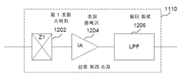
도 2는 본 공개의 실시예에 따른 신호 처리 소자(1110)의 예시적인 계략도를 도시한다. 도 1에 따른 신호 처리 소자(1110)는 제 1 초퍼 스위치(Z1)(1202) 및 제 1 초퍼 증폭기(IA)(1204)를 포함한다. 제 1 초퍼 스위치(1202)는 베이스밴드 주파수 및 초퍼 주파수 상에서 개별적으로 운반되는 편차 신호 및 자계 신호를 분리하도록 구성된다. 제 1 초퍼 증폭기(1204)는 편차 신호 및 자계 신호를 증폭하여 전송을 위하여 증폭된 편차 신호 및 자계 신호를 초퍼 주파수 및 베이스밴드 주파수로 각각 스위칭하도록 구성된다. 특정 실시예에서, 초퍼 주파수는 100KHz보다 더 크며 베이스밴드 주파수는 200Hz보다 더 작다.FIG. 2 illustrates an exemplary schematic diagram of a
특정 실시예에서, 외부 전원이 AC 전원일 때, 베이스밴드 주파수는 AC 전원의 주파수에 비례한다. 특정 실시예에서, 베이스밴드 주파수는 AC 전원의 주파수보다 2배이다.In a particular embodiment, when the external power source is an AC power source, the baseband frequency is proportional to the frequency of the AC power source. In certain embodiments, the baseband frequency is twice the frequency of the AC power source.
특정 실시예에서, 신호 처리 소자(1110)는 초퍼 주파수를 통해 전송되는 편차 신호를 제거하도록 구성되는 저역 필터(LPF)(1206)를 더 포함할 수 있다.In a particular embodiment, the
본 실시예에서, 제 1 초퍼 스위치(Z1)(1202), 제 1 초퍼 증폭기(IA)(1204) 및 저역 필터(LPF)(1206)의 입력 및 출력의 각각은 단일 선으로 도시된다. 도 2는 설명적인 목적인 것이 이해되어야 한다. 본 공개는 한정적인 것으로 의도되지 않는다. 제 1 초퍼 스위치(Z1)(1202), 제 1 초퍼 증폭기(IA)(1204) 및 저역 필터(LPF)(1206)의 입력 및 출력은 하나 이상의 입/출력 신호가 될 수 있다. 특정 실시예에서, 제 1 초퍼 스위치(Z1)(1202), 제 1 초퍼 증폭기(IA)(1204) 및 저역 필터(LPF)(1206)의 입/출력 각각은 차동 신호의 하나 이상의 쌍을 포함한다.In this embodiment, each of the inputs and outputs of the first chopper switch (Z1) 1202, the first chopper amplifier (IA) 1204 and the low-pass filter (LPF) 1206 is shown as a single line. It should be understood that FIG. 2 is for illustrative purposes. The disclosure is not intended to be limiting. The inputs and outputs of the first chopper switch (Z1) 1202, the first chopper amplifier (IA) 1204 and the low pass filter (LPF) 1206 may be one or more input / output signals. In a particular embodiment, each of the inputs / outputs of a first chopper switch (Z1) 1202, a first chopper amplifier (IA) 1204 and a low-pass filter (LPF) 1206 includes one or more pairs of differential signals .
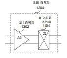
도 3A는 본 공개의 실시예에 따른 초퍼 증폭기(1204)의 예시적인 개략도를 도시한다. 도 2의 제 1 초퍼 증폭기(IA)(1204)는 제 1 증폭기(A1)(1302) 및 제 2 초퍼 스위치(Z2)(1304)를 포함한다. 제 1 증폭기(A1)(1302)는 제 1 초퍼 스위치(Z1)(1202)로부터 편차 신호 및 자계 신호의 제 1 단계(stage) 증폭을 수행하도록 구성된다. 특정 실시예에서, 제 1 증폭기(A1)(1302)는 1112와 같이 적어도 하나의 폴드형 캐스케이드 증폭기를 사용하여 구현된다. 제 2 초퍼 스위치(Z2)(1304)는 전송을 위하여 증폭된 편차 신호 및 자계 신호를 초퍼 주파수 및 베이스밴드 주파수로 각각 스위칭하도록 구성된다.3A shows an exemplary schematic diagram of a
도 3B는 본 공개의 다른 실시예에 따른 초퍼 증폭기(1204)의 예시적인 개략도를 도시한다. 도시된 실시예에 있어서, 도 2의 제 1 초퍼 증폭기(IA)(1204)는 제 1 증폭기(A1)(1302) 및 제 2 초퍼 스위치(Z2)(1304)에 더하여 제 2 증폭기(A2)(1306)를 더 포함한다. 제 2 증폭기(A2)(1306)는 제 2 초퍼 스위치(Z2)(1304)로부터의 자계 신호 및 편차 신호의 제 2 단계 증폭을 더 수행하도록 구성된다. 특정 실시예에서, 제 2 초퍼 스위치(Z2)(1304)는 단일단(single-stage) 증폭기를 기초로 구현된다.3B illustrates an exemplary schematic diagram of a
도 3b의 제 1 증폭기(A1)(1302), 제 2 초퍼 스위치(Z2)(1304) 및 제 2 증폭기(A2)(1306)의 연결이 설명적인 목적을 위한 것임이 이해되어야 한다. 본 공개는 한정적인 것으로 의도되지 않는다. 특정 실시예에서, 제 2 증폭기(A2)(1306)는 제 1 증폭기(A1)(1302)와 제 2 초퍼 스위치(Z2)(1304) 사이에 배치될 수 있다.It should be understood that the connection of the first amplifier A1, 1302, the second
도 4는 본 공개의 다른 실시예에 따른 자기 센서의 예시적인 개략도를 도시한다. 본 공개에 따른 자기 센서는 입력 포트(1408), 정류기 회로(1402), 자계 검출 회로(1404), 출력 제어 회로(1406) 및 출력 포트(1410)를 포함한다. 본 실시예의 입력 포트(1408)는 외부 전원에 연결되는 입력 포트(1408A 및 1408B)의 한 쌍을 포함한다. 특정 실시예에서, 입력 포트(1408)는 외부 전원에 직렬로 연결될 수 있다. 또 다른 실시예에서, 입력 포트(1408)는 외부 전원에 병렬로 연결될 수 있다.Figure 4 shows an exemplary schematic diagram of a magnetic sensor according to another embodiment of the present disclosure. The magnetic sensor according to the present disclosure includes an
정류기 회로(1402)는 전파 정류기 브릿지 및 전압 조정기(미도시)를 기초로 구현될 수 있다. 전파 정류기 브릿지는 AC 전원으로부터의 AC 신호를 DC 신호로 변환하도록 구성될 수 있다. 전압 조정기는 미리 설정된 범위 내의 DC 신호를 조절하도록 구성될 수 있다. 정류기 회로(1402)는 자계 검출 회로(1404) 및 출력 제어 회로(1406)에 조절된 DC 신호를 공급한다.The
도시된 실시예에서, 자계 검출 회로(1404)는 홀 검출기(1420), 제 1 초퍼 스위치(1422), 제 1 초퍼 증폭기(1424), 샘플 앤드 홀드 회로(1426), 필터 회로(1428) 및 비교기 회로(comparator circuit)(1430)를 포함한다. 홀 검출기(1420)는 자계 신호를 검출하며 제 1 초퍼 스위치(1422)에 검출된 자계 신호를 출력하도록 정류기 회로(1402)에 연결된다. 제 1 초퍼 스위치(1422)는 도 2에 도시되는 제 1 초퍼 스위치(1202)와 동일한 기능을 수행하도록 구성된다. 제 1 초퍼 스위치(1422)는 차동 신호{P1, N1}의 제 1 쌍을 제 1 초퍼 증폭기(1424)에 출력한다.In the illustrated embodiment, the magnetic
제 1 초퍼 증폭기(1424)는 도 3b에 도시되는 것을 기초로 구현될 수 있다. 그러므로, 제 1 초퍼 증폭기(1424)는 제 1 증폭기(A1)(1302), 제 2 초퍼 스위치(Z2)(1304) 및 제 2 증폭기(A2)(1306)를 포함한다. 제 1 증폭기(A1)(1302)는 수신된 제 1 쌍의 차동 신호{P1, N1}의 제 1 단계 증폭을 수행한다. 제 2 초퍼 스위치(Z2)(1304)는 제 1 클록 반주기에서 증폭된 차동 신호{P1, N1}를 직접 출력하며, 제 2 클록 반주기에서 출력하도록 증폭된 차동 신호{P1, N1}를 스위칭하도록 구성된다. 제 2 초퍼 스위치(Z2)(1304)는 차동 신호{P2, N2}의 제 2 쌍을 출력한다. 차동 신호{P2, N2}의 제 2 쌍은 샘플 앤드 홀드 회로(1426)로 출력되기 전에 제 2 증폭기(A2)(1306)에 의해 더 증폭될 수 있다.The
샘플 앤드 홀드 회로(1426)는 제 1 클록 반주기와 제 2 클록 반주기 동안 도 4에서 제 1 초퍼 증폭기(1424)로부터 출력되는 증폭된 제 2 쌍의 차동 신호{P2, N2}를 각각 샘플링하도록 구성된다. 샘플 앤드 홀드 회로(1426)의 출력은 2쌍의 차동 신호{P2A , N2A} 및{P2B, N2B}를 포함하고, 여기서, 한 쌍의{P2A, N2A}는 제 1 클록 반주기 동안 출력되며, 한 쌍의{P2B, N2B}는 제 2 클록 반주기 동안 출력된다.The sample and hold
필터 회로(1428)는 두 쌍의 차동 신호{P2A , N2A} 및{P2B, N2B}로부터 편차 신호를 제거하고, 차동 신호{P2A , N2A} 및{P2B, N2B}를 증폭하며 비교기 회로(1430)에 제 3 차동 신호{P3, N3}를 출력하도록 구성된다.The
비교기 회로(1430)는 기준 전압 신호 한 쌍과 차동 신호{P3, N3}를 비교하여 비교 결과를 기초로 외부 자계의 극성을 결정하도록 구성된다. 비교기 회로(1430)는 외부 자계의 결정된 극성을 표시하는 자계 검출 신호를 생성하며 이것을 출력 제어 회로(1406)에 출력한다. 특정 실시예에서, 자계 검출 신호는 스위칭 자계 검출 신호이다.The
출력 제어 회로(1406)는 외부 자계의 결정된 극성에 응하여 일 상태에서 동작하도록 자기 센서를 제어하도록 구성된다. 자기 센서는 복수의 상태에서 동작할 수 있다. 예컨대, 제 1 상태는 부하 전류가 출력 포트(1410)를 통해 자기 센서의 내부에서 외부로 흐르는 시나리오에 상응할 수 있으며, 제 2 상태는 부하 전류가 출력 포트(1410)를 통해 자기 센서의 외부로부터 내부로 흐르는 시나리오에 상응할 수 있다. 특정 실시예에서, 자기 센서는 출력 포트(1410)를 통해 전류가 흐르지 않는 제 3 상태에서 동작할 수 있다.The
실제 자기 전압 신호는 일반적으로 매우 작다. 예컨대, 밀리볼트보다 작은 것이 공통적이다. 그러나, 홀 검출기(1420)에 의해 생성되는 편차 신호는 종종, 더 높고, 거의 10 밀리볼트이다. 본 공개는 편차 신호를 제거하고 실제 자기 전압 신호를 증폭하고자 하므로, 동작가능한 레벨에서의 실제 자기 전압 신호는 모터 또는 자기 센서를 사용하는 임의의 전기 장비에 제공될 수 있다. 특정 실시예에서, 자계 검출 회로(1404)에 대한 전압 공급은 약 2.5V의 레벨이다. 홀 검출기(1420)에 의해 출력되는 검출 신호가 제 1 초퍼 스위치(1422), 제 1 초퍼 증폭기(1424), 샘플 앤드 홀드 회로(1426) 및 필터 회로(1428)를 통과할 때, 검출된 신호는 기존 전력 이득의 1000배 내지 2000배, 바람직하게는 기존 전력 이득의 1600배와 같이 그 사이의 임의의 수로 증폭될 수 있다. 결과적으로, 검출된 실제 자기 전압 신호는 자계 검출 회로(1404)에 공급되는 전압 레벨의 대략 절반이 되도록 증폭된다. 특정 실시예에서, 제 1 초퍼 증폭기(1424)는 필터 회로(1428)의 이득보다 더 큰 이득을 성취하도록 구성된다. 예컨대, 제 1 초퍼 증폭기(1424)에 의해 성취된 이득은 50일 수 있으며 필터 회로(1428)에 의해 성취된 이득은 32이다.The actual magneto voltage signal is generally very small. For example, it is smaller than millivolts. However, the deviation signal generated by the
도 5는 본 공개의 일 실시예에 따르는 정류기 회로(1402)의 예시적인 개략도를 도시한다. 도 5에 도시된 실시예에 따르면, 전파 정류기 브릿지는 제 1 다이오드(1502), 제 2 다이오드(1504), 제 3 다이오드(1506) 및 제 4 다이오드(1508)를 포함하는 정류기 회로(1402)를 구현하도록 사용되며; 전압 조정기는 조정기 다이오드(1520)를 포함한다. 제 1 다이오드(1502) 및 제 2 다이오드(1504)는 직렬로 연결된다. 제 3 다이오드(1506) 및 제 4 다이오드(1508)는 또한 직렬로 연결된다. 제 1 다이오드(1502)의 캐소드 및 제 2 다이오드(1504)의 어노드는 입력 포트(1408A)에 연결하도록 구성되며, 이것은 전압(VAC +)을 공급한다. 제 3 다이오드(1506)의 캐소드 및 제 4 다이오드(1508)의 어노드는 입력 포트(1408B)에 연결하도록 구성되며, 이것은 전압(VAC -)을 공급한다. 조정기 다이오드(1502)의 어노드는 제 3 다이오드(1506) - 그라운드에 추가로 연결됨 - 및 제 1 다이오드(1502)의 어노드에 연결되도록 구성된다. 조정기 다이오드(1520)의 캐소드는 전압(VDD)에 함께 연결되는 제 4 다이오드(1508) 및 제 2 다이오드(1504)의 캐소드에 연결된다.FIG. 5 illustrates an exemplary schematic diagram of a
도 6은 본 공개의 일 실시예에 따르는 홀 검출기(1420) 및 제 1 초퍼 스위치의 예시적인 회로도를 도시한다. 도시된 실시예에 따르면, 홀 검출기(1420) 및 제 1 초퍼 스위치(1422)는 도 6의 단일 회로로서 집적된다. 홀 검출기(1420)는 4개의 연결 포트(1602, 1604, 1606 및 1608)를 갖는 홀 검출 회로 기판을 포함한다. 연결 포트(1602 및 1606)는 서로 대향하게 배치되며 연결 포트(1604 및 1608)는 서로 대향하게 배치된다. 제 1 초퍼 스위치(1422)는 4개의 스위치(1610, 1612, 1614 및 1616)를 포함한다. 스위치(1610)는 연결 포트(1602 및 1608)가 교번하여 전원(VCC)에 연결되도록 제어하며 스위치(1612)는 연결 포트(1604 및 1606)가 교번하여 그라운드에 연결되도록 제어한다. 스위치(1614)는 연결 포트(1602 및 1608)가 교번하여 차동 신호(P1)를 출력하도록 제어하며 스위치(1616)는 연결 포트(1604 및 1606)가 교번하여 차동 신호(N1)를 출력하도록 제어한다. 특정 실시예에서, 홀 검출기(1420) 및 제 1 초퍼 스위치(1422)는, 연결 포트(1602 및 1608) 중 하나가 전원(VCC)에 연결될 때, 연결 포트(1602 및 1608) 중 다른 하나는 차동 신호(P1)를 출력하도록 구성된다. 한편, 연결 포트(1604 및 1606) 중 하나가 그라운드에 연결될 때, 연결 포트(1604 및 1606) 중 다른 하나는 차동 신호(N1)를 출력한다. 예컨대, 연결 포트(1602)가 전원(VCC) 및 연결 포트(1606)에 연결될 때, 연결 포트(1608 및 1604)는 차동 신호{P1, N1}의 한 쌍을 출력한다. 대안적으로, 연결 포트(1608)가 전원(VCC)에 연결되며 연결 포트(1604)를 그라운드에 연결할 때, 연결 포트(1602 및 1606)는 차동 신호{P1, N1}의 제 1 쌍을 출력한다.6 illustrates an exemplary circuit diagram of a
특정 실시예에서, 전원(VCC)은 정류기 회로(1402)의 출력의 전압 강하 및 조절을 수행함으로써 성취되는 정전압원일 수 있다. 다른 실시예에서, 전원(VCC)은 정전류원일 수 있다.In a particular embodiment, the power supply ( VCC ) may be a constant voltage source that is accomplished by performing voltage drop and regulation of the output of the
특정 실시예에서, 각각의 스위치(1610, 1612, 1614 및 1616)는 고전압 전도 또는 저전압 전도가 되도록 구성되는 한 쌍의 스위치를 포함한다. 이러한 쌍의 스위치의 각각은 상보적인 클록 신호의 한 쌍에 의해 제어될 수 있다. 동일한 주파수의 상보적인 클록 신호의 2쌍을 스위치(1610, 1612, 1614 및 1616)에 각각 공급함으로써, 홀 검출기(1420) 및 제 1 초퍼 스위치(1422)는 제 1 쌍의 차동 신호{P1, N1}를 생성할 수 있다.In a particular embodiment, each of the
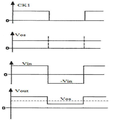
도 7은 도 6의 회로도에 따른 예시적인 신호 출력을 도시한다. 신호(CK1)는 클록 신호를 표시한다. 신호(Vos)는 홀 검출기(1420)에서 고유한 편차 신호를 표시한다. 일반적으로, 신호(Vos)는 홀 검출기(1420)의 물리적인 특성에 의존한다. Vin and -Vin 는 클록 신호(CK1)의 제 1 절반 및 제 2 절반 동안 각각 제 1 초퍼 스위치(1422)에 의해 출력되는 실제 자계 전압 신호를 표시한다. 실제 자계 전압 신호는 편차 신호에 의해 유발된 간섭 신호 없이 외부 자계와 관련되는 이상적인 자계 전압 신호이다. 클록 신호(CK1)의 제 1 절반 및 제 2 절반 동안, 제 1 초퍼 스위치(1422)에 의해 출력되는 실제 자계 전압 신호는 동일한 진폭 및 반대되는 극성을 갖는다. Vout는 편차 신호(Vos)에 의해 또는 그와 결합하는 실제 자계 전압 신호(Vin 또는 -Vin)인 제 1 초퍼 스위치(1422)의 출력을 표시한다. 제 1 초퍼 스위치(1422)는 실제 자계 전압 신호(Vin 또는 -Vin)와 편차 신호(Vos)를 분리하고 이 신호를 각각 초퍼 주파수 및 베이스밴드 주파수상으로 스위칭한다. 특정 실시예에서, 초퍼 주파수는 클록 신호(CK1)의 주파수이며 베이스밴드 주파수는 외부 자계의 주파수를 변경하는 극성이다.FIG. 7 illustrates an exemplary signal output according to the circuit diagram of FIG. The signal CK1 indicates a clock signal. The signal Vos indicates a deviation signal inherent in the
도 8은 본 공개의 일 실시예에 따르는 필터 회로(1428)의 예시적인 회로도를 도시한다. 도 4에 도시된 바와 같은 필터 회로(1428)는 제 1 필터(F1)(1802) 및 제 2 필터(F2)(1804)를 포함할 수 있다. 제 1 필터(F1)(1802)는 샘플 앤드 홀드 회로(1426)로부터 출력되는 신호{P2A , P2B} 및{N2A, N2B}의 2개의 쌍의 각각에 더하여 제 1 단계를 적용하도록 구성되며, 이것은 편차 신호를 제거하기 위한 것이다. 제 1 필터(F1)(1802)는 제 1 단계 추가 공정 이후 신호 상에서의 제 1 단계 이득 증폭을 수행하도록 추가로 구성될 수 있다. 제 2 필터(F2)(1804)는 제 1 필터(F1)(1802)로부터의 출력 신호에 대한 제 2 단계 추가 및/또는 제 2 단계 이득 증폭을 적용하고 차동 신호{P3, N3}의 제 3 쌍을 생성하도록 구성된다. 제 1 필터(F1)(1802)의 이득은 제 2 필터(F2)(1804)의 이득보다 더 작도록 구성될 수 있다. 예컨대, 제 1 필터(F1)(1802)의 이득은 4이며 제 2 필터(F2)(1804)의 이득은 8이다.FIG. 8 illustrates an exemplary circuit diagram of a
상기 기재된 필터 회로(1428)의 도면은 설명적인 목적을 위한 것임이 이해되어야 한다. 본 공개는 한정적인 것으로 의도되어서는 안된다. 필터 회로(1428)는 도 8에 도시된 것보다 많거나 적은 필터를 포함할 수 있다. 특정 실시예에서, 필터 회로(1428)는 단 하나의 필터를 포함할 수 있다. 그러나, 이러한 상황에서, 유일한 필터는 더 나은 이득을 성취하기 위하여 큰 저항을 갖고 구성되어야 할 수 있다.It should be appreciated that the illustration of the
도 9는 본 공개의 일 실시예에 따른 비교기 회로(1430)의 예시적인 회로도를 도시한다. 도 4의 비교기 회로(1430)는 도 1의 A/D 변환 소자(1114)와 동일한 기능을 수행할 수 있다. 본 실시예에서, 비교기 회로(1430)는 제 1 비교기(C1)(1902), 제 2 비교기(C2)(1904) 및 래치 논리 회로(S)(1906)를 포함하는 지연 비교기일 수 있다. 제 1 비교기(C1)(1902)에 대한 입력은 차동 신호{P3, N3}의 제 3 쌍 및 기준 전압 신호{Vh , Vl}의 한 쌍을 포함하고, Vh는 고전압 신호이며 Vl는 저전압 신호이다. 제 2 비교기(C2)(1904)에 대한 입력은, 기준 전압 신호{Vh , Vl}의 쌍이 반대 극성에 연결되는 것을 제외하고 제 1 비교기(C1)에 입력되는 신호의 동일한 쌍을 포함한다. 제 1 비교기(C1)(1902)는 필터(1408)로부터 출력 전압(V1)을 컴퓨팅하도록 구성되고, 여기서, V1=P3-N3이고, 고전압 임계값은 Rh이며, Rh= Vh - Vl이다. 제 1 비교기(C1)(1902)는 출력 전압(V1)을 고전압 임계값(Rh)에 비교한다. V1> Rh일 때, 제 1 비교기(C1)(1902)는 높게 출력하고 V1< Rh일 때, 제 1 비교기(C1)(1902)는 낮게 출력한다. 제 2 비교기(C2)(1904)는 낮은 전압 임계값(V1)과 필터(1408)로부터의 출력 전압(Rl)을 비교하도록 구성되고, Rl = Vl - Vh이다. V1> Rl일 때, 제 2 비교기(C2)(1904)는 높게 출력하고 V1<Rl일 때, 제 2 비교기(C2)(1904)는 낮게 출력한다. Rh이 Rl보다 클 때, V1> Rh일 때, V1> Rl를 의미하고, 제 1 비교기(C1)(1902) 및 제 2 비교기(C2)(1904)는 높게 출력한다. V1< Rl일 때, V1<Rh를 의미하고, 제 1 비교기(C1)(1902) 및 제 2 비교기(C2)(1904)는 낮게 출력한다. Rl <V1< Rh일 때, 제 1 비교기(C1)(1902)는 낮게 출력하며 제 2 비교기(C2)(1904)는 높게 출력한다. 제 1 비교기(C1)(1902) 및 제 2 비교기(C2)(1904)로부터의 비교 결과는 래치 논리 회로(S)(1906)에 보내진다. 래치 논리 회로(S)(1906)는 비교 결과를 기초로 전압 신호를 생성하도록 구성된다. 전압 신호는 자기 센서의 동작 상태를 제어하도록 출력 제어 회로(1406)로 더 보내진다. 래치 논리 회로(S)(1906)가 비교 결과를 기초로 전압 신호를 생성하는 방법에 대한 상세가 이하에서 기재된다.FIG. 9 illustrates an exemplary circuit diagram of a
도 10은 본 공개의 일 실시예에 따른 자계의 극성을 결정하기 위한 예시적인 개략도를 도시한다. 래치 논리 회로(S)(1906)가 필터 회로(1428)의 출력 전압(V1)이 Rh보다 더 큰 것을 표시하는 제 1 비교기(C1)(1902) 및 제 2 비교기(C2)(1904)로부터의 비교 결과를 수신할 때, 래치 논리 회로(S)(1906)는 싱크 전류 상태로의 변화를 표시하는 제 1 신호를 생성한다. 래치 논리 회로(S)(1906)가 필터 회로(1428)의 출력 전압이 Rl보다 더 작은 것을 표시하는 제 1 비교기(C1)(1902) 및 제 2 비교기(C2)(1904)로부터의 비교 결과를 수신할 때, 래치 논리 회로(S)(1906)는 소스 전류 상태로의 변화를 표시하는 제 2 신호를 생성한다. 래치 논리 회로(S)(1906)가 필터 회로(1428)의 출력 전압(V1)이 Rl <V1<Rh를 충족하는 것을 표시하는 제 1 비교기(C1)(1902) 및 제 2 비교기(C2)(1904)로부터의 비교 결과를 수신할 때, 래치 논리 회로(S)(1906)는 상태 변화가 없음을 표시하는 제 3 신호를 생성한다. 특정 실시예에서, 제 1 전압은 외부 자계가 제 1 극성을 나타내는 것을 표시하며, 제 2 전압은 외부 자계가 제 2 극성을 표시하는 것을 나타낸다.10 illustrates an exemplary schematic diagram for determining the polarity of a magnetic field in accordance with one embodiment of the present disclosure. The latch logic circuit (S) 1906 outputs a signal from the first comparator (C1) 1902 and the second comparator (C2) 1904 indicating that the output voltage V1 of the
도 10은 특정 실시예에서, 외부 자계의 자계 강도가 동작 지점(Bop)에 도달할 때, 비교기 회로(1430)는 제 1 신호를 생성하고, 외부 자계의 자계 강도가 릴리스 지점(Brp)의 아래일 때, 비교기 회로(1430)는 제 2 신호를 생성하며, 외부 자계의 자계 강도는 동작 지점(Bop)과 릴리스 지점(Brp) 사이일 때, 비교기 회로(1430)는 변화 없이 출력된 전류로 남는다.10, in a particular embodiment, when the magnetic field strength of the external magnetic field reaches the operating point Bop, the
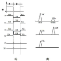
도 11은 본 공개의 일 실시예에 따른 클록 주기의 예시적인 신호 출력을 도시한다. 도 11a에 도시된 바와 같이, 차동 신호{P1, N1}의 제 1 쌍은 제 1 초퍼 스위치(1422)의 출력이고, 차동 신호{P2, N2}의 제 2 쌍은 제 1 초퍼 증폭기(1424)의 출력이며, 차동 신호{P3, N3}의 제 3 쌍은 필터 회로(1428)의 출력이다.{P1A, N1A}는 제 1 클록 반주기 동안 제 1 초퍼 스위치(1422)로부터 출력되는 차동 신호의 한 쌍이며,{P1B, N1B}는 제 2 클록 반주기 동안 제 1 초퍼 스위치(1422)로부터 출력되는 차동 신호의 한 쌍이다.{P2A, N2A}는 제 1 클록 반주기동안 제 1 초퍼 증폭기(1424)로부터 출력되는 차동 신호의 한 쌍이며{P2B, N2B}는 제 2 클록 반주기 동안 제 1 초퍼 증폭기(1424)로부터 출력되는 차동 신호의 한 쌍이다.11 illustrates an exemplary signal output of a clock period in accordance with one embodiment of the present disclosure. 11A, the first pair of differential signals { P1, N1 } is the output of the
상기 기재된 바와 같이, Vout은 제 1 초퍼 스위치(1422)의 출력을 표시하고, 이것은 편차 신호(Vos)에 의해 중첩되는 실제 자계 전압 신호(Vin 또는 -Vin)이다. 다른 측면에서, Vout은 차동 신호{P1, N1}의 제 1 쌍의 사이의 차이를 표시하고, P1 및 N1는 동일한 진폭 및 반대되는 극성을 갖는다. 그러므로, P1A, P1B, N1A 및 N1B 는 이하의 식에 의해 표시된다:As described above, Vout represents the output of the

도 4의 제 1 초퍼 증폭기(1424)가 도 3b에 도시된 실시예를 구현할 때, 제 1 초퍼 증폭기(1424)는 제 1 증폭기(A1)(1302), 제 2 초퍼 스위치(Z2)(1304) 및 제 2 증폭기(A2)(1306)를 포함한다. 제 1 쌍의 차동 신호{P1, N1}는 제 1 증폭기(A1)(1302)를 통과한 후 차동 신호{P1', N1'}로 증폭된다.{P1', N1'} 및 제 1 클록 반주기 및 제 2 클록 반주기 동안 그 개별적인 구성요소는 이하의 식에 의해 표시된다:When
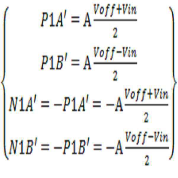
A는 제 1 증폭기(A1)(1302)의 증폭 이득을 표시한다. Voff는 제 1 증폭기(A1)(1302)에 의해 출력되는 편차 신호를 표시하고, 이것은 홀 검출기(1420)에 의해 생성되는 편차 신호(Vos) 및 제 1 증폭기(A1)(1302)에 의해 생성되는 편차 신호를 포함한다. 설명적인 목적에 있어서, 계수 A 및 ½는 본 명세서에서 이하의 기재로부터 무시된다. A represents the amplification gain of the first amplifier (A1) 1302. [ Voff represents the deviation signal output by the first amplifier (A1) 1302, which is applied to the
제 2 초퍼 스위치(Z2)(1304)는 직접 제 1 클록 반주기에 증폭된 차동 신호{P1, N1}를 출력하고, 제 2의 제 2 클록 반주기에 증폭된 차동 신호{P1, N1}를 스위칭식으로(switchingly) 출력하며, 제 2 초퍼 스위치(Z2)(1304)로부터의 출력은 각각의 클록 반주기에서의 2개의 구성요소를 포함한다. 샘플 앤드 홀드 회로(1426)를 통과한 후, 이하의 식에 의해 표시되는 4개의 구성요소{P2A , P2B , N2A , N2B}가 필터 회로(1428)에 입력된다.2 a chopper switch (Z2) (1304) is directly first differential signal {P1, N1} of outputs, the differential signal {P1, N1} amplified with the second clock half-period of the second amplifier to the clock half-period switching formula And the output from the second
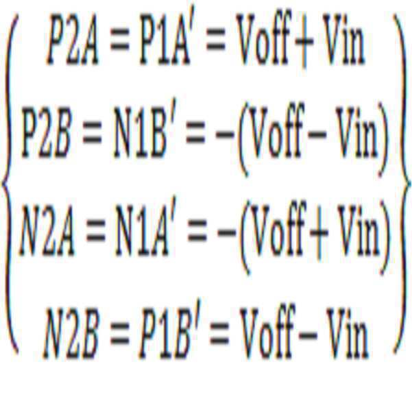
또한, 필터 회로(1428)에 의해 출력되는 차동 신호{P3, N3}의 제 3 쌍은 이하의 식에 의해 표시된다:The third pair of differential signals { P3, N3 } output by the

상기 식에 도시된 바와 같이, 차동 신호{P3, N3}의 제 3 쌍의 편차 신호는 필터 회로(1428)에 의해 제거된다. 차동 신호{P3, N3}의 제 3 쌍은, 따라서, 실제 자계 전압 신호만을 포함한다.As shown in the above equation, the third pair of deviation signals of the differential signals { P3, N3 } are removed by the
도 11B는 제 1 초퍼 스위치(예컨대, 도 2의 1202) 후, 실제 자계 전압 신호(Vin) 및 편차 신호(Voff)는 400kHz의 초퍼 주파수 및 100Hz의 베이스밴드 주파수로 각각 분리되는 것을 도시하며, 여기서 초퍼 주파수는 클록 신호의 주파수이다. 제 2 초퍼 스위치(예컨대, 도 3a, 도 3b의 1304) 후, 실제 자계 전압 신호(Vin) 및 편차 신호(Voff)는 각각 베이스밴드 주파수 및 초퍼 주파수로 스위칭된다. 이어서, 필터 회로(예컨대, 도 2의 1206) 후, 편차 신호(Voff)는 필터링 아웃 된다. 자기 센서가 동기식 모터를 제어하도록 구현될 때, 외부 자계는 영구 자석 모터 필드일 수 있으며, 여기서 극성 변경 주파수는 AC 전력원 주파수의 2배이다. 동기식 모터에 50Hz 또는 60Hz의 시티 AC 전원이 제공될 경우, 베이스밴드 주파수는 100Hz 또는 120Hz이다. 다수의 초퍼 스위치 및 증폭기를 통과한 후, 실제 자계 전압 신호 및 편차 신호는 매우 넓은 주파수에서 분리된다. 이처럼, 본 공개에서 구현되는 초퍼 증폭기는 매우 넓은 주파수 범위를 수용하도록 구성된다.11B shows that the actual field voltage signal Vin and the deviation signal Voff are separated by a chopper frequency of 400 kHz and a baseband frequency of 100 Hz , respectively, after the first chopper switch (e.g., 1202 in Fig. 2) , Where chopper frequency is the frequency of the clock signal. After the second chopper switch (e.g., 1304 in FIGS. 3A and 3B), the actual magnetic field voltage signal Vin and the deviation signal Voff are switched to the baseband frequency and the chopper frequency, respectively. Then, after the filter circuit (e.g., 1206 in FIG. 2), the deviation signal Voff is filtered out. When the magnetic sensor is implemented to control a synchronous motor, the external magnetic field may be a permanent magnet motor field, where the polarity change frequency is twice the AC power source frequency. If the AC power provided by the city of 50 Hz or 60 Hz in the synchronous motor, the baseband frequency is 100 Hz or 120 Hz. After passing through a number of chopper switches and amplifiers, the actual magnetic field voltage signal and the deviation signal are separated at a very wide frequency. As such, the chopper amplifiers implemented in this disclosure are configured to accommodate a very wide frequency range.
도 12는 본 공개의 일 실시예에 따른 출력 제어 회로(1406)의 예시적인 회로도를 도시한다. 도시된 실시예에 따른 출력 제어 회로(1406)는 제 1 스위치(2202) 및 제 2 스위치(2204)를 포함한다. 제 1 스위치(2202)는 제 1 전류 경로를 형성하도록 출력 포트(1410)와 결합되며, 제 2 스위치(2204)는 제 2 전류 경로를 형성하도록 출력 포트(1410)와 결합된다. 전류는 반대 방향으로 제 1 전류 경로와 제 2 전류 경로를 통해 흐른다. 제 1 스위치(2202) 및 제 2 스위치(2204)는 선택적으로 연결될 자기 검출 신호에 의해 제어된다. 특정 실시예에서, 제 1 스위치(2202)는 트랜지스터이며, 제 2 스위치(2204)는 다이오드 또는 트랜지스터이다.12 shows an exemplary circuit diagram of an
특정 실시예에서, 제 1 스위치(2202)는 저전압 패스(low voltage pass)로서 구성되며 제 2 스위치(2204)는 고전압 패스(high voltage pass)로 구성된다. 제 1 스위치(2202) 및 제 2 스위치(2204) 모두의 제어 단부는 자기 검출 회로(1404)의 출력에 연결된다. 제 1 스위치(2202)의 출력 및 제 2 스위치(2204)의 입력은 출력 포트(1410)에 모두 연결된다. 제 1 스위치(2202)의 입력은 예컨대, 정류기 회로(1402)로부터의 출력(VDD) 또는 DC 전력원과 같이 고전압 단부(2206)에 연결될 수 있으며, 제 2 스위치(2204)의 출력은 예컨대 그라운드와 같이 저전압 단부(2208)에 연결될 수 있다.In a particular embodiment, the
자기 검출 회로(1404)의 출력이 낮은 전압 신호인 경우, 제 1 스위치(2202)가 연결되고, 제 2 스위치(2204) 분리된다. 결과적으로, 부하 전류는 고전압 단부(2206)로부터 제 1 스위치(2202) 내로 흘러 출력 포트(1410)를 통해 밖으로 흐른다. 자기 검출 회로(1404)의 출력이 고전압 신호인 경우, 제 2 스위치(2204)는 연결되고, 제 1 스위치(2202)는 분리된다. 결과적으로, 부하 전류에서 출력 포트(1410)로부터 제 2 스위치(2204) 내로의 흘러 저전압 단부(2208)를 통해 밖으로 흐른다.When the output of the
도 13는 본 공개의 다른 실시예에 따른 출력 제어 회로의 예시적인 회로도를 도시한다. 도시된 실시예에 따른 출력 제어 회로(1406)는 제 1 스위치(2302) 및 제 2 스위치(2304)를 포함한다. 제 1 스위치(2302)는 고전압 패스로 구성되며 제 2 스위치(2304)는 일방향 다이오드가 되도록 구성된다. 제 1 스위치(2302)의 제어 단부 및 제 2 스위치(2304)의 캐소드는 자기 검출 회로(1404)의 출력에 모두 연결된다. 특정 실시예에서, 제 1 스위치(2302)의 제어 단부는 저항(2308)을 통해 자기 검출 회로(1404)의 출력에 연결된다. 제 1 스위치(2302)의 입력은 정류기 회로(1402)의 출력에 연결될 수 있다(도 4 참조). 제 1 스위치(2302)의 출력 및 제 2 스위치의 어노드는 출력 포트(1410)에 모두 연결된다. 도 12에 도시된 실시예와 유사하게, 제 1 스위치(2302)는 제 1 전류 경로를 형성하도록 출력 포트(1410)와 결합되고, 제 2 스위치(2304)는 제 2 전류 경로를 형성하도록 출력 포트(1410)와 결합된다. 전류는 반대 방향인 제 1 및 제 2 전류 경로를 통해 흐른다. 자기 검출 회로(1404)의 출력이 고전압 신호일 경우, 제 1 스위치(2302)는 연결되며 제 2 스위치(2304)는 분리된다. 결과적으로, 부하 전류는 고전압 단부(2306)로부터 제 1 스위치(2302) 내로 흐르며, 출력 포트(1410)를 통해 밖으로 흐른다. 자기 검출 회로(1404)의 출력은 저전압 신호일 경우, 제 2 스위치(2304)는 연결되며 제 1 스위치(2302)는 분리된다. 결과적으로, 부하 전류는 출력 포트(1410)로부터 제 2 스위치(2304) 내로 흐른다.Figure 13 shows an exemplary circuit diagram of an output control circuit according to another embodiment of the present disclosure. The
도 14는 본 공개의 또 다른 실시예에 따라 출력 제어 회로의 예시적인 회로도를 도시한다. 도시된 실시예의 출력 제어 회로(1406)는 단방향 스위치(2402) 및 저항(2404)을 포함한다. 단방향 스위치(2402)는 제 1 전류 경로를 형성하도록 자계 검출 회로(1404)와 출력 포트(1410) 사이에서 연결되며 저항(2404)은 제 2 전류 경로를 형성하도록 자계 검출 회로(1404)와 출력 포트(1410) 사이에서 연결되며, 여기서, 전류는 반대 방향인 제 1 및 제 2 전류 경로를 통해 흐른다. 자기 검출 회로(1404)의 출력이 고전압 신호일 경우, 단방향 스위치(2402)는 연결되며 부하 전류는 단방향 스위치(2402)를 통해 자계 검출 회로(1404)의 출력에서 출력 포트(1410)로 흐른다. 자기 검출 회로(1404)의 출력이 저전압 신호일 경우, 단방향 스위치(2402)는 분리되며 부하 전류는 저항(2404)을 통해 출력 포트(1410)로부터 자기 검출 회로(1404)의 출력으로 흐른다.Figure 14 illustrates an exemplary circuit diagram of an output control circuit in accordance with another embodiment of the present disclosure; The
본 공개의 자기 센서는 추가 A/D 변환 장비가 필요하지 않는 시티 AC 전원에 직접 연결될 수 있다. 그러므로, 본 공개는 다양한 분야로의 자기 센서의 구현을 가능하게 한다. 또한, 자계 검출 회로는 검출된 자계 신호를 효율적으로 증폭하고, 전압을 조절하여 간섭 신호를 필터링할 수 있다. 그러므로, 자기 센서는 전기 회전자의 동작을 제어하도록 외부 자계의 극성에 관하여 더 정확한 신호를 생성할 수 있다.The magnetic sensors of the present disclosure can be connected directly to a city AC power source that does not require additional A / D conversion equipment. Therefore, the present disclosure enables the implementation of magnetic sensors in various fields. In addition, the magnetic field detection circuit can efficiently amplify the detected magnetic field signal and filter the interference signal by adjusting the voltage. Therefore, the magnetic sensor can generate a more accurate signal about the polarity of the external magnetic field to control the operation of the electric rotor.
도 15는 본 공개에 따라 구성된 자기 센서를 통합하는 모터(2500)의 예시적인 개략도를 도시한다. 모터는 AC 전원(2502), 모터(2504), 자기 센서(2508) 및 양방향 스위치(2510)를 포함할 수 있다. 특정 실시예에서, 모터(2500)는 자기 센서(2508)에 제공하기 전에 AC 전원(2502)의 레벨을 제거하도록 구성되는 전압 강하 회로(2506)를 더 포함할 수 있다. 자기 센서(2508)의 출력(Pout)은 양방향 스위치(2510)의 제어 단부에 전기 연결된다.Figure 15 shows an exemplary schematic diagram of a
특정 실시예에서, 자기 센서(2508)는 AC 전원(2502)이 포지티브 반주기에서 동작할 때 그리고 자기 센서(2508)의 자계 검출 회로(1404)가 외부 자계가 제 1 극성을 나타냄을 결정할 때 양방향 스위치(2510)에 구동 전류를 출력하도록 구성된다. 대안적으로, 자기 센서(2508)의 출력 제어 회로(1406)는 AC 전원(2502)이 네거티브 반주기에서 동작할 때 그리고 자계 검출 회로(1404)가 외부 자계가 제 1 극성의 반대인 제 2 극성을 나타냄을 결정할 때 자기 센서(2508)가 양방향 스위치(2510)에 구동 전류를 출력하도록 구성된다. 자기 센서(2508)의 출력 제어 회로(1406)는, AC 전원(2502)이 네거티브 반주기에서 동작하고 자계 검출 회로(1404)가 외부 자계가 제 1 극성을 나타냄을 결정할 때, 또는 AC 전원(2502)은 포지티브 반주기에서 동작하며 자계 검출 회로(1404)가 제 2 극성을 나타냄을 결정할 때, 자기 센서(2508)가 양방향 스위치(2510)로 구동 전류를 출력하지 않도록 제어하도록 추가로 구성된다.In a particular embodiment, the
자기 센서(2508)가 도 5에 도시된 정류기 회로 및 도 12에 도시된 출력 제어 회로를 사용하는 실시예에서, 도 12의 제 1 스위치(2202)의 입력은 도 5의 브릿지 전파 정류기의 전압 출력(VDD)에 연결하도록 구성되며 제 2 스위치(2204)의 출력은 그라운드에 연결하도록 구성된다. AC 전원(2502)이 포지티브 반주기에서 동작하고 자계 검출 회로(1404)가 저전압을 출력할 때, 제 1 스위치(2202)는 연결되며 제 2 스위치는 분리되고, 전류는 AC 전원(2502), 모터(2504), VAC +, 자기 센서(2508) 및 양방향 스위치(2510)를 통과하는 한 방향으로 흐른다. 자기 센서(2508) 내에서, 전류는 브릿지 전파 정류기의 전압 출력 및 제 1 스위치(2202)를 통해 흐른다. 특정 실시예에서, 전류는 자기 센서(2508)전에 전압 강하 회로(2506)를 통해 흐른다.In the embodiment in which the
AC 전원(2502)이 네거티브 반주기에서 동작하고 자계 검출 회로(1404)가 고전압을 출력할 때, 제 1 스위치(2202)는 분리되며 제 2 스위치는 연결되고, 전류는 AC 전원(2502), 양방향 스위치(2510), 자기 센서(2508) 및 모터(2504)를 통과하는 반대 방향으로 흐른다. 자기 센서(2508) 내에서, 전류는 제 2 스위치(2204), 브릿지 전파 정류기의 그라운드 출력, 제 1 다이오드(1502) 및 VAC +를 통해 흐른다. AC 전원(2502)이 포지티브 반주기에서 동작하고 자계 검출 회로(1404)가 고전압을 출력할 때, 또는 AC 전원(2502)이 네거티브 반주기에서 동작하고 자계 검출 회로(1404)가 저전압을 출력할 때, 제 1 스위치(2202) 및 제 2 스위치(2204)는 모두 분리된다. 결과적으로, 자기 센서(2508)의 Pout를 통해 흐르는 구동 전류는 존재하지 않는다.When the
도 16은 본 공개에 따라 구성되는 자기 센서를 통합하는 동기식 모터(2600)의 예시적인 개략도를 도시한다. 동기식 모터(2600)는 고정자 및 고정자에 대하여 회전하도록 구성되는 회전자(2602)를 포함한다. 고정자는 고정자 코어(2604) 및 고정자 코어(2604) 주변에 감기도록 구성되는 고정자 코일(2612)을 포함한다. 고정자 코어(2604)는 철, 주철, 전기 강, 규소 등과 같은 임의의 연성 자기 물질로 구성될 수 있다. 회전자(2602)는 AC 전원이 직렬로 연결될 때, 60f/p의 일정한 속도(즉, 분당 회전수, rpm)에서 회전하도록 구성되며, 여기서, f는 AC 전원의 주파수이며 p는 회전자(2602)의 극 쌍의 수이다. 고정자 코어(2604)는 대향하는 극 부분(2608A 및 2608B)의 상으로 구성된다. 대향하는 극 부분(2608A 및 2608B)의 쌍의 각각은 극호 표면, 예컨대, 2610A 및 2610B을 갖는다. 회전자(2602)의 표면은 극호 표면(2610A, 2610B)에 반대되며 그 사이에 공극(2606)을 형성한다. 특정 실시예에서, 회전자(2602)와 고정자 사이의 공극(2606)은 매우 작은 고르지 않은 갭(gap) 영역을 대부분 가지며 고르다. 특정 실시예에서, 극 표면(2610A, 2610B)의 각각은 시작 그루브, 예컨대 2614로 더 구성된다. 극호 표면(2610A, 2610B)은 시작 그루브의 영역을 제외하고 회전자(2602)와 동심이다. 시작 그루브의 구성은 고르지 않은 자계를 내부에 형성한다. 또한, 시작 그루브의 구성은, 회전자(2602)가 정지 상태일 때, 회전자(2602)의 극(S1)이 극 부분(2608A 및 2608B)의 중심 극(S2)에 대한 각으로 경사진다. 이러한 구성은, 회전자(2602)가 모터가 턴 온될 때마다 시작 토크를 갖는 것을 허용한다. 본 실시예에서, 회전자(2602)의 극(S1)은 회전자(2602)의 2개의 자극 사이의 분리 경계이며, 중심 극(S2)은 중앙의 대향하는 극 부분(2608A 및 2608B)을 통과한다. 고정자 및 회전자(2602)는 모두 2개의 자극을 갖고 구성된다.16 illustrates an exemplary schematic diagram of a
본 공개에 따른 출력 제어 회로(1406)는 AC 전원(2502)의 극성 및 외부 자계의 극성을 기초로 연결 및 분리 사이의 상태를 스위칭하도록 양방향 스위치(2510)를 제어하고 또한 고정자 코일(2612)의 전력 증가 상태를 제어한다. 이처럼, 고정자에 의해 생성되는 자계는 하나의 단일 방향으로 회전자가 회전하도록 구동하도록 회전자(2602)의 자계 위치와 공조하고 모터가 모터의 전력이 증가할 때마다 일정한 회전 방향을 갖는 것을 보장할 수 있다.The
상술한 실시예는 예시적인 목적을 위한 것으로 이해되어야 한다. 본 공개는 한정적인 것으로 의도되지 않는다. 고정자 및 회전자(2602)는 4개 또는 6개의 자극과 같이 상이한 자극으로 구성될 수 있다. 또한, 고정자 및 회전자(2602)는 서로에 대해 상이한 자극을 가질 수 있다.It should be understood that the above-described embodiments are for illustrative purposes only. The disclosure is not intended to be limiting. The stator and
당업자는, 본 공개는 다양한 변형 및/또는 개선을 위해 다룰 수 있음을 인지할 것이다. 예컨대, 호스트 장치와 본 명세서에 개시된 바와 같이, 클라이언트 노드는 펌웨어, 펌웨어/소프트웨어의 조합, 펌웨어/하드웨어 조합, 또는 하드웨어/펌웨어/소프트웨어 조합으로서 구현될 수 있다. 상기 기재된 다양한 구성요소의 구현이 하드웨어 장치에서 이행될 수 있지만, 이것은 또한 소프트웨어 전용 솔루션 - 예컨대, 기존 서버상에서의 설치 - 으로서 구현될 수 있다. 또한, 본 명세서에 개시된 바와 같이 호스트의 유닛 및 클라이언트 노드는 펌웨어, 펌웨어/소프트웨어 조합, 펌웨어/하드웨어 조합, 또는 하드웨어/펌웨어/소프트웨어 조합으로서 구현될 수 있다.Those skilled in the art will recognize that the disclosure may be adapted for various modifications and / or improvements. For example, as described herein with the host device, the client node may be implemented as firmware, firmware / software combination, firmware / hardware combination, or hardware / firmware / software combination. While the implementation of the various components described above may be implemented in a hardware device, it may also be implemented as a software-only solution, e.g., an installation on an existing server. Further, the unit and client nodes of the host may be implemented as firmware, firmware / software combination, firmware / hardware combination, or hardware / firmware / software combination as disclosed herein.
전술한 것이 최상의 모드 및/또는 다른 예로 간주되는 것으로 기재되었으나, 이는 다양한 변형이 이루어질 수 있고 본 명세서에 개시된 대상이 다양한 형태 및 실시예로 구현될 수 있으며, 상기 교시는 다수의 응용에 적용될 수 있고, 그 일부만이 본 명세서에 설명되는 것이 이해된다. 다음의 청구범위에 의해, 본 공개의 진정한 범위 내에 있는 임의의 모든 응용, 변형 및 변화가 청구되도록 의도된다.While the foregoing is considered to be the best mode and / or example, it is to be understood that various modifications may be made and the objects disclosed herein may be implemented in various forms and embodiments, , Only some of which are described herein. It is intended by the following claims to cover any and all applications, modifications and variations that fall within the true scope of the disclosure.
Claims (10)
외부 전원에 연결되는 입력 포트;
자기 검출 신호를 생성하도록 구성되는 자계 검출 회로;
자기 검출 신호에 응답하여 자기 센서의 동작을 제어하도록 구성된 출력 제어 회로; 및
출력 포트를 포함하되,
상기 자계 검출 회로는:
외부 자계를 검출하고 검출 신호를 출력하도록 구성되는 자기 감지 소자,
상기 검출 신호를 증폭하고 상기 검출 신호로부터의 간섭을 제거하여 처리된 검출 신호를 생성하도록 구성되는 신호 처리 소자, 및
처리된 검출 신호를 상기 자기 센서를 적어도 상기 자기 검출 신호에 응답하여 제1 상태 및 제2 상태 중 적어도 하나에서 동작하도록 제어하는데 이용되는 상기 자기 검출 신호로 변환하도록 구성되는 변환 소자를 포함하되,
제1 상태에서, 부하 전류는 출력 포트로부터 자기 센서의 외부로 흐르고, 또한
제2 상태에서, 부하 전류는 상기 자기 센서의 외부로부터 출력 포트로 흐르며,
상기 신호 처리 소자는 증폭기 및 필터 회로를 포함하며, 상기 증폭기의 이득은 상기 필터 회로의 이득보다 더 큰, 자기 센서.As a magnetic sensor:
An input port connected to an external power source;
A magnetic field detection circuit configured to generate a magnetic detection signal;
An output control circuit configured to control an operation of the magnetic sensor in response to the magnetic detection signal; And
Output ports,
The magnetic field detection circuit comprising:
A magnetic sensing element configured to detect an external magnetic field and output a detection signal,
A signal processing element configured to amplify the detection signal and remove the interference from the detection signal to generate a processed detection signal; and
And a conversion element configured to convert the processed detection signal into the magnetic detection signal used to control the magnetic sensor to operate in at least one of a first state and a second state in response to at least the magnetic detection signal,
In the first state, the load current flows from the output port to the outside of the magnetic sensor,
In the second state, the load current flows from the outside of the magnetic sensor to the output port,
Wherein the signal processing element comprises an amplifier and a filter circuit, the gain of the amplifier being greater than the gain of the filter circuit.
상기 검출 신호는 자계 신호 및 편차 신호를 포함하며,
상기 증폭기는 초퍼 증폭기이며, 또한
상기 필터 회로는 저역 필터이고,
상기 신호 처리 소자는:
상기 검출 신호를 각각 초퍼 주파수 및 베이스밴드 주파수에 대응하는 상기 편차 신호 및 상기 자계 신호로 분리하도록 구성되는 제1 초퍼 스위치를 포함하고,
상기 초퍼 증폭기는 상기 편차 신호 및 상기 자계 신호를 증폭하고, 증폭된 편차 신호 및 증폭된 자계 신호를 각각 초퍼 주파수 및 베이스밴드 주파수 상으로 스위칭하도록 구성되고, 또한
상기 필터 회로는 상기 초퍼 주파수에서 상기 편차 신호를 필터링 아웃(filter out)하도록 구성되는, 자기 센서. The method according to claim 1,
Wherein the detection signal includes a magnetic field signal and a deviation signal,
The amplifier is a chopper amplifier,
Wherein the filter circuit is a low pass filter,
Wherein the signal processing element comprises:
And a first chopper switch configured to separate the detection signal into the deviation signal and the magnetic field signal corresponding to the chopper frequency and the baseband frequency, respectively,
Wherein the chopper amplifier is configured to amplify the deviation signal and the magnetic field signal and to switch the amplified deviation signal and the amplified magnetic field signal on chopper frequency and baseband frequency respectively,
Wherein the filter circuit is configured to filter out the deviation signal at the chopper frequency.
제1 증폭기; 및
제2 초퍼 스위치를 포함하되,
상기 제1 증폭기는 상기 제1 초퍼 스위치로부터의 상기 편차 신호 및 상기 자계 신호에 대해 제1 단계 증폭을 수행하여 각각 증폭된 상기 편차 신호 및 증폭된 상기 자계 신호를 생성하도록 구성되며, 또한
상기 제2 초퍼 스위치는 상기 증폭된 편차 신호 및 증폭된 자계 신호를 초퍼 주파수 및 베이스밴드 주파수 상으로 스위칭하도록 구성되는, 자기 센서.The chopper amplifier according to claim 2, wherein the chopper amplifier
A first amplifier; And
And a second chopper switch,
Wherein the first amplifier is configured to perform a first stage amplification on the deviation signal and the magnetic field signal from the first chopper switch to generate the amplified deviation signal and the amplified magnetic field signal,
And the second chopper switch is configured to switch the amplified deviation signal and the amplified magnetic field signal onto a chopper frequency and a baseband frequency.
상기 제2 증폭기는 상기 초퍼 주파수 상으로 스위칭되는 증폭된 편차 신호 및 상기 베이스밴드 주파수 상으로 스위칭되는 증폭된 자계 신호에 대해 제2 단계 증폭을 수행하도록 구성되며, 상기 제1 증폭기의 이득은 상기 제2 증폭기의 이득보다 큰, 자기 센서.4. The chopper amplifier of claim 3, wherein the chopper amplifier further comprises a second amplifier disposed between the second chopper switch and the filter circuit,
Wherein the second amplifier is configured to perform a second stage amplification on an amplified deviation signal switched on the chopper frequency and an amplified magnetic field signal switched on the baseband frequency, 2 < / RTI > amplifier.
상기 샘플 앤드 홀드 회로는 각각 제1 클록 반주기 및 제2 클록 반주기 동안 제1 쌍의 차동 신호를 샘플링하고, 클록 주기 동안 두 쌍의 샘플링된 차동 신호를 출력하도록 구성되는, 자기 센서.3. The apparatus of claim 2, wherein the signal processing element further comprises a sample and hold circuit coupled between the chopper amplifier and the filter circuit,
Wherein the sample and hold circuit is configured to sample a first pair of differential signals during a first clock half period and a second clock half period and output two pairs of sampled differential signals during a clock period.
상기 외부 전원은 교류(AC) 전원이며,
상기 자기 검출 신호는 스위칭 검출 신호이며,
상기 자기 검출 신호의 스위칭 주파수는 상기 AC 전원의 주파수에 비례하거나 또는 상기 AC 전원의 주파수의 2배인, 자기 센서.The method according to claim 1,
The external power source is an alternating current (AC) power source,
The magnetic detection signal is a switching detection signal,
Wherein the switching frequency of the magnetic detection signal is proportional to the frequency of the AC power source or twice the frequency of the AC power source.
외부 전원에 연결되는 입력 포트;
출력 포트; 및
자기 검출 신호를 생성하도록 구성되며,
외부 자계를 검출하고 검출 신호를 출력하도록 구성되는 자기 감지 소자 - 상기 검출 신호는 자계 신호 및 편차 신호를 포함함 - ,
상기 검출 신호를 증폭하고 상기 검출 신호로부터의 간섭을 제거하여 처리된 검출 신호를 생성하도록 구성되는 신호 처리 소자, 및
처리된 검출 신호를 상기 자기 센서를 적어도 상기 자기 검출 신호에 응답하여 제1 상태 및 제2 상태 중 적어도 하나에서 동작하도록 제어하는데 이용되는 상기 자기 검출 신호로 변환하도록 구성되는 변환 소자를 포함하되,
상기 신호 처리 소자는
상기 검출 신호를 각각 초퍼 주파수 및 베이스밴드 주파수에 대응하는 상기 자계 신호 및 상기 편차 신호로 분리하도록 구성되는 제1 초퍼 스위치;
상기 자계 신호 및 상기 편차 신호를 개별적으로 증폭하고 증폭된 편차 신호 및 증폭된 자계 신호를 각각 초퍼 주파수 및 베이스밴드 주파수 상으로 스위칭하도록 구성된 초퍼 증폭기, 및
상기 초퍼 주파수로 스위칭된 상기 편차 신호를 제거하도록 구성되는 필터 회로를 포함하되,
상기 초퍼 증폭기의 이득은 상기 필터 회로의 이득보다 더 큰 집적 회로.An integrated circuit for a magnetic sensor comprising:
An input port connected to an external power source;
Output port; And
And to generate a magnetic detection signal,
A magnetic sensing element configured to detect an external magnetic field and output a detection signal, the detection signal including a magnetic field signal and a deviation signal,
A signal processing element configured to amplify the detection signal and remove the interference from the detection signal to generate a processed detection signal; and
And a conversion element configured to convert the processed detection signal into the magnetic detection signal used to control the magnetic sensor to operate in at least one of a first state and a second state in response to at least the magnetic detection signal,
The signal processing element
A first chopper switch configured to separate the detection signal into the magnetic field signal and the deviation signal corresponding to chopper frequency and baseband frequency, respectively;
A chopper amplifier configured to amplify the magnetic field signal and the deviation signal separately and to switch the amplified deviation signal and the amplified magnetic field signal respectively on chopper frequency and baseband frequency,
And a filter circuit configured to remove the deviation signal switched to the chopper frequency,
Wherein the gain of the chopper amplifier is greater than the gain of the filter circuit.
Applications Claiming Priority (6)
| Application Number | Priority Date | Filing Date | Title |
|---|---|---|---|
| CNPCT/CN2015/086422 | 2015-08-07 | ||
| PCT/CN2015/086422 WO2016019921A1 (en) | 2014-08-08 | 2015-08-07 | Motor assembly and integrated circuit for motor drive |
| CN201610205912 | 2016-04-01 | ||
| CN201610205912.1 | 2016-04-01 | ||
| CN201610392144.5 | 2016-06-02 | ||
| CN201610392144.5A CN106443524A (en) | 2015-08-07 | 2016-06-02 | Magnetic sensor integrated circuit, motor assembly and application device |
Publications (1)
| Publication Number | Publication Date |
|---|---|
| KR20170017841A true KR20170017841A (en) | 2017-02-15 |
Family
ID=57466866
Family Applications (1)
| Application Number | Title | Priority Date | Filing Date |
|---|---|---|---|
| KR1020160100329A Withdrawn KR20170017841A (en) | 2015-08-07 | 2016-08-05 | A magnetic sensor and an integratred circuit |
Country Status (5)
| Country | Link |
|---|---|
| JP (2) | JP2017090439A (en) |
| KR (1) | KR20170017841A (en) |
| BR (1) | BR102016018233A2 (en) |
| DE (2) | DE102016114588A1 (en) |
| MX (1) | MX2016010278A (en) |
Families Citing this family (4)
| Publication number | Priority date | Publication date | Assignee | Title |
|---|---|---|---|---|
| CN109298233A (en) * | 2018-11-30 | 2019-02-01 | 国网电力科学研究院武汉南瑞有限责任公司 | An AC and DC current sensor |
| JP7260321B2 (en) * | 2019-02-15 | 2023-04-18 | エイブリック株式会社 | magnetic sensor circuit |
| CN111999521B (en) * | 2020-09-23 | 2024-11-26 | 安徽容知日新科技股份有限公司 | A speed sensor and a signal indicating circuit |
| FR3146381A1 (en) * | 2023-03-01 | 2024-09-06 | Valeo Eautomotive Germany Gmbh | Electrical machine with a sensor and improved insulation test for said sensor |
-
2016
- 2016-08-05 KR KR1020160100329A patent/KR20170017841A/en not_active Withdrawn
- 2016-08-05 DE DE102016114588.2A patent/DE102016114588A1/en not_active Withdrawn
- 2016-08-05 DE DE202016104335.2U patent/DE202016104335U1/en not_active Expired - Lifetime
- 2016-08-08 JP JP2016155744A patent/JP2017090439A/en active Pending
- 2016-08-08 BR BR102016018233A patent/BR102016018233A2/en not_active Application Discontinuation
- 2016-08-08 MX MX2016010278A patent/MX2016010278A/en unknown
- 2016-12-12 JP JP2016005930U patent/JP3211276U/en not_active Expired - Fee Related
Also Published As
| Publication number | Publication date |
|---|---|
| JP2017090439A (en) | 2017-05-25 |
| DE202016104335U1 (en) | 2016-11-16 |
| JP3211276U (en) | 2017-07-06 |
| MX2016010278A (en) | 2017-12-01 |
| DE102016114588A1 (en) | 2017-02-09 |
| BR102016018233A2 (en) | 2016-12-27 |
Similar Documents
| Publication | Publication Date | Title |
|---|---|---|
| US10469005B2 (en) | Magnetic sensor and an integrated circuit | |
| US9696182B2 (en) | Magnetic sensor and an integrated circuit | |
| JP5406010B2 (en) | Motor drive circuit | |
| KR20170017841A (en) | A magnetic sensor and an integratred circuit | |
| US9692329B2 (en) | Magnetic sensor and an integrated circuit | |
| CN205982596U (en) | Magnetic sensor integrated circuits, motor components and application equipment | |
| JP2017227626A (en) | Magnetic sensor integrated circuit, motor assembly and application apparatus | |
| CN107315149B (en) | Magnetic sensor integrated circuit, motor assembly and application equipment | |
| WO2013168353A1 (en) | Magnetic detection device and magnetic detection method | |
| CN106443515A (en) | Magnetic sensor integrated circuit, motor assembly, and application equipment | |
| US10199965B2 (en) | Magnetic sensor integrated circuit, motor assembly and application apparatus | |
| CN205982595U (en) | Magnetic sensor integrated circuits, motor components and application equipment | |
| US20170310254A1 (en) | Magnetic sensor integrated circuit, motor assembly and application device | |
| KR20170017837A (en) | A magnetic sensor and an integrated circuit | |
| KR20170017844A (en) | A magnetic sensor and an integrated circuit | |
| CN107005751B (en) | Drive control device and drive control system having the same | |
| CN205982597U (en) | Magnetic sensor integrated circuits, motor components and application equipment | |
| JP3209222U (en) | Magnetic sensor, integrated circuit and motor assembly | |
| JP3211277U (en) | Magnetic sensor and control method of operation stage thereof | |
| JP3209053U (en) | Magnetic sensor integrated circuit, motor assembly and application apparatus | |
| US10454397B2 (en) | Magnetic sensor integrated circuit, motor assembly and application apparatus | |
| JP3209223U (en) | Magnetic sensor, motor assembly and integrated circuit |
Legal Events
| Date | Code | Title | Description |
|---|---|---|---|
| PA0109 | Patent application |
Patent event code: PA01091R01D Comment text: Patent Application Patent event date: 20160805 |
|
| PG1501 | Laying open of application | ||
| PC1203 | Withdrawal of no request for examination | ||
| WITN | Application deemed withdrawn, e.g. because no request for examination was filed or no examination fee was paid |