KR20170013331A - Integrated circuit with cooling array - Google Patents
Integrated circuit with cooling array Download PDFInfo
- Publication number
- KR20170013331A KR20170013331A KR1020167036633A KR20167036633A KR20170013331A KR 20170013331 A KR20170013331 A KR 20170013331A KR 1020167036633 A KR1020167036633 A KR 1020167036633A KR 20167036633 A KR20167036633 A KR 20167036633A KR 20170013331 A KR20170013331 A KR 20170013331A
- Authority
- KR
- South Korea
- Prior art keywords
- cooling
- contact area
- thermoelectric
- integrated circuit
- elements
- Prior art date
Links
Images


Classifications
-
- H—ELECTRICITY
- H01—ELECTRIC ELEMENTS
- H01L—SEMICONDUCTOR DEVICES NOT COVERED BY CLASS H10
- H01L23/00—Details of semiconductor or other solid state devices
- H01L23/34—Arrangements for cooling, heating, ventilating or temperature compensation ; Temperature sensing arrangements
- H01L23/38—Cooling arrangements using the Peltier effect
-
- H01L35/32—
-
- H—ELECTRICITY
- H10—SEMICONDUCTOR DEVICES; ELECTRIC SOLID-STATE DEVICES NOT OTHERWISE PROVIDED FOR
- H10N—ELECTRIC SOLID-STATE DEVICES NOT OTHERWISE PROVIDED FOR
- H10N10/00—Thermoelectric devices comprising a junction of dissimilar materials, i.e. devices exhibiting Seebeck or Peltier effects
- H10N10/10—Thermoelectric devices comprising a junction of dissimilar materials, i.e. devices exhibiting Seebeck or Peltier effects operating with only the Peltier or Seebeck effects
- H10N10/17—Thermoelectric devices comprising a junction of dissimilar materials, i.e. devices exhibiting Seebeck or Peltier effects operating with only the Peltier or Seebeck effects characterised by the structure or configuration of the cell or thermocouple forming the device
-
- H—ELECTRICITY
- H10—SEMICONDUCTOR DEVICES; ELECTRIC SOLID-STATE DEVICES NOT OTHERWISE PROVIDED FOR
- H10N—ELECTRIC SOLID-STATE DEVICES NOT OTHERWISE PROVIDED FOR
- H10N19/00—Integrated devices, or assemblies of multiple devices, comprising at least one thermoelectric or thermomagnetic element covered by groups H10N10/00 - H10N15/00
-
- H—ELECTRICITY
- H01—ELECTRIC ELEMENTS
- H01L—SEMICONDUCTOR DEVICES NOT COVERED BY CLASS H10
- H01L2924/00—Indexing scheme for arrangements or methods for connecting or disconnecting semiconductor or solid-state bodies as covered by H01L24/00
- H01L2924/0001—Technical content checked by a classifier
- H01L2924/0002—Not covered by any one of groups H01L24/00, H01L24/00 and H01L2224/00
-
- H—ELECTRICITY
- H10—SEMICONDUCTOR DEVICES; ELECTRIC SOLID-STATE DEVICES NOT OTHERWISE PROVIDED FOR
- H10N—ELECTRIC SOLID-STATE DEVICES NOT OTHERWISE PROVIDED FOR
- H10N19/00—Integrated devices, or assemblies of multiple devices, comprising at least one thermoelectric or thermomagnetic element covered by groups H10N10/00 - H10N15/00
- H10N19/101—Multiple thermocouples connected in a cascade arrangement
Abstract
본 발명은 냉각 어레이를 형성하는 적어도 하나의 열전 컴포넌트(thermoelectric component)(1)의 구현을 위한 도핑(doped) 및 구분(distinguished) 영역을 갖는 유전체 기판으로 구성되는, 바람직하게는 마이크로프로세서 또는 냉각 장치를 위한, 집적회로 냉각 어레이에 관한 것이다. 냉각 어레이는, 열전 컴포넌트가 적어도 하나의 제1 접촉 영역(contact area), 적어도 하나의 제2 접촉 영역 및 적어도 하나의 냉각 섹션(cooling section)을 포함하고, 냉각 섹션이 제1 접촉 영역과 제2 접촉 영역 사이에 배치되어, 제어 유닛을 통해 제1 접촉 영역과 제2 접촉 영역에 의해 전압이 공급되는 적어도 하나의 써멀 엘리먼트(thermal element)(29)로 구성되며, 써멀 엘리먼트(29)가 브리지 엘리먼트(53, 58, 59, 73, 83, 84, 92)에 의해 연결되는 방식으로 되는 적어도 하나의 도핑 층 및 제2 도핑 층으로 구성되고, 브리지 엘리먼트(53, 58, 59, 73, 83, 84, 92)는 제1 도핑 층 및/또는 제2 도핑 층 위에만 부분적으로 놓이는 것을 특징으로 한다. 본 발명에 따른 냉각 어레이의 의하면, 집적회로의 내부로부터 충분히 자유로운 열 흐름(heat flow)이 보장되기 때문에, 컴팩트하고 및/또는 더 효율적인 집적회로들이 구현될 수 있다.The present invention is preferably a microprocessor or cooling device comprising a dielectric substrate having a doped and distinguished area for the implementation of at least one thermoelectric component 1 forming a cooling array, To an integrated circuit cooling array. The cooling array is characterized in that the thermoelectric component comprises at least one first contact area, at least one second contact area and at least one cooling section, the cooling section comprising a first contact area and a second contact area, And at least one thermal element (29) arranged between the contact areas and supplied with a voltage by the first contact area and the second contact area via the control unit, wherein the thermal element (29) And at least one doping layer and a second doping layer in such a manner that they are connected by a first doping layer (53, 58, 59, 73, 83, 84, 92) , 92) are partially located only over the first doping layer and / or the second doping layer. In the case of a cooling array according to the invention, compact and / or more efficient integrated circuits can be realized, since a sufficiently free heat flow from the interior of the integrated circuit is ensured.
Description
본 발명은 냉각 어레이를 형성하는 적어도 하나의 열전 컴포넌트(thermoelectric component)의 구현을 위한 도핑(doped) 및 구분(distinguished) 영역을 갖는 기판으로 구성되는, 바람직하게 마이크로프로세서 또는 냉각 장치들을 위한, 집적회로 냉각 어레이(integrated circuit cooling array)에 관한 것이다. 부가적으로, 적어도 마이크로전자 컴포넌트(microelectronic component)가 집적회로 냉각 어레이에 의해 냉각되는 기판 위에 또는 기판 내에 형성될 수 있다.The present invention relates to an integrated circuit, preferably for a microprocessor or cooling device, consisting of a substrate with a doped and distinguished area for the implementation of at least one thermoelectric component forming a cooling array, To an integrated circuit cooling array. Additionally, at least a microelectronic component may be formed on or in the substrate to be cooled by the integrated circuit cooling array.
바람직하게, 마이크로프로세서의 구현을 위한 집적회로들은 일반적으로 금속, 반도체들 또는 유전체 매체들의 복잡한 배치로 구성되고, 유전체 매체로 구성된 기판 위에 소정의 레이아웃 및 형성 순서로 배치된다. 그 상황에서 매우 제한된 공간에서 전자 회로들을 구현하는 옵션이 존재하는데, 층 구성 및 도핑을 위한 서로 다른 방법을 포함하는 반도체 기술에 기인한다. 이런 방법의 사용으로, 서브미크론(submicron) 레벨로 잘 정의된(well-defined) 두께 및 잘 정의된 형태의 층 뿐만 아니라 잘 정의된 도핑을 생산한다. 스퍼터 증착, 빔 증착, 증기 코팅, 이온 플레이팅(물리적 기상 증착), 화학적 기상 증착, 갈바닉 코팅, 이온 주입, 중성자 변환 도핑 및 확산 도핑의 방법이 여기서 언급되어야 한다.Preferably, the integrated circuits for the implementation of the microprocessor generally consist of complex arrangements of metals, semiconductors or dielectric media and are arranged in a predetermined layout and forming order on a substrate made of dielectric medium. In that circumstance, there is an option to implement electronic circuits in a very limited space, due to semiconductor technology, which includes different methods for layer construction and doping. The use of this method produces a well-defined doping as well as a well-defined thickness and a well-defined layer at the submicron level. Methods of sputter deposition, beam deposition, vapor deposition, ion plating (physical vapor deposition), chemical vapor deposition, galvanic coating, ion implantation, neutron conversion doping and diffusion doping should be mentioned here.
따라서, 매우 제한된 공간에서 고도로 복잡한 전자 회로들을 생산하는 것이 가능해졌지만, 전자 회로의 성능증가에 따라, 전력 소모도 증가한다. 증가된 전력 소모는 다시 집적회로의 마이크로전자 엘리먼트들의 증가된 열 방출, 및 결과적으로 전체의 열 발생을 수반한다. 하지만, 집적회로에서 방출되는 열은 집적회로에 해로우며, 때로는 영구적일 수도 있는, 임계 온도에 도달할 때 이들의 기능 능력(functioning ability)의 손실을 초래할 수도 있다. 따라서, 집적회로의 성능 및 따라서 그 복잡성이 감소되어야 하고, 또는 집적회로의 능동적인 냉각이 발생해야 한다. 능동적인 냉각 시스템과 관련하여, 특히 콤팩트하고 매우 효율적인 집적회로가 구현될 수 있다. 하지만, 집적회로에서 발생하는 열이 먼저 표면에 도달하기 전에 냉각 시스템을 통과해야 하기 때문에, 집적회로의 전력 소비 및 복잡성은 능동적인 냉각 시스템에서도 제한된다.Thus, it is possible to produce highly complex electronic circuits in very limited space, but as the performance of electronic circuits increases, power consumption also increases. The increased power consumption is again accompanied by increased heat dissipation of the microelectronic elements of the integrated circuit, and consequently overall heat generation. However, the heat released from the integrated circuit may be detrimental to the integrated circuit, and may result in a loss of their functioning ability when the critical temperature is reached, which may be permanent. Thus, the performance of the integrated circuit and hence its complexity must be reduced, or active cooling of the integrated circuit must occur. With respect to active cooling systems, particularly compact and highly efficient integrated circuits can be implemented. However, the power consumption and complexity of the integrated circuit is limited in active cooling systems as the heat generated in the integrated circuit must pass through the cooling system before it reaches the surface first.
집적회로 내부에서의 능동적인 냉각은 종래 기술에 따른 소위 펠티어(Peltier) 엘리먼트들의 사용에 의해 가능하다. 펠티어 엘리먼트들은 가변하는 전기 전도도를 갖는 2개의 컴포턴트들로 구성되는, 써멀 엘리먼트들(thermal elements)의 직렬 시퀀스(serial sequence)이다. 두 컴포넌트들은 전기적으로 전도성인, 소위 브리지(bridge)에 의해 연결된다. 2개의 써멀 엘리먼트들은 각각 브리지에 의해 연결되고, 각 브리지는 동일 또는 인접하는 써멀 엘리먼트의 제1 컴포넌트와 제2 컴포넌트 사이의 전기적 연결을 제공한다. 2개의 컴포넌트들은 일반적으로 n-도핑 반도체 소재(n-doped semiconducting material) 및 p-도핑 반도체 소재이다. 이러한 2개의 컴포넌트들은 종종 금속성 브리지에 의해 대부분 전기적으로 연결된다. p-도핑 반도체 소재의 전도대(conduction band)의 에너지 준위는 동일하지만 n-도핑 반도체 소재의 전도대의 에너지 준위는 다르기 때문에, 전자들(electrons)이 컴포넌트들 중 하나로부터 다른 컴포넌트로 통과할 때, 열 에너지가 주변으로부터 흡수되거나 또는 열 에너지가 주변으로 방출되고, 이는 전자들이 제1 컴포넌트로부터 제2 컴포넌트로 통과하는지 또는 반대로 통과하는지 여부에 의존한다. 따라서, 전류가 흐르는 동안, 브리지와 컴포넌트 사이의 접촉 영역으로부터 주변들(surroundings)로의 열 방출 또는 주변들로부터의 열 흡수가 발생하며, 열 전달의 방향은 제1 및 제2 컴포넌트들의 소재들 및 전류 흐름의 방향에 의존한다. 그 주변들은 집적회로의 임베딩(embedding) 소재 및 추가 마이크로전자 컴포넌트들에 의해 형성된다.Active cooling inside the integrated circuit is possible by the use of so-called Peltier elements according to the prior art. Peltier elements are a serial sequence of thermal elements, consisting of two components with varying electrical conductivities. The two components are connected by an electrically conductive, so-called bridge. The two thermal elements are each connected by a bridge, and each bridge provides an electrical connection between the first and second components of the same or adjacent thermal elements. The two components are generally n-doped semiconducting material and p-doped semiconductor material. These two components are often mostly electrically connected by a metallic bridge. Since the energy level of the conduction band of the p-doped semiconductor material is the same but the energy level of the conduction band of the n-doped semiconductor material is different, when the electrons pass from one of the components to the other, Energy is absorbed from the surroundings or heat energy is emitted to the surroundings, which depends on whether the electrons pass from the first component to the second component or vice versa. Thus, during current flow, heat is dissipated from the contact area between the bridge and the components to surroundings or from the ambient, and the direction of heat transfer is dependent on the materials of the first and second components, It depends on the direction of the flow. The perimeters are formed by the embedding material of the integrated circuit and additional microelectronic components.
펠티어 엘리먼트의 더 따뜻한(warmer) 측으로부터 방출된 열은 외부 냉각 시스템의 보조로, 예를 들어 냉각 디바이스(device) 및 그 위에 배치된 팬의 보조로 소산되어야 한다. 펠티어 엘리먼트가 집적회로 내에 배치되면, 열은 열 채널들(heat channels)을 통해 집적회로의 표면으로 전달되고, 다음에 소산될 수 있다.The heat emitted from the warmer side of the Peltier element must be dissipated with the aid of an external cooling system, for example, with the aid of a cooling device and a fan disposed thereon. When the Peltier element is placed in an integrated circuit, the heat is transferred to the surface of the integrated circuit through heat channels and then dissipated.
펠티어 엘리먼트들을 통해 집적회로 내에서 달성될 수 있는 이러한 냉각 시스템에도 불구하고, 집적회로의 전력 소비 및 복잡성은 제한된다. 이것은 집적회로의 내부로부터 외부로의 시간 단위당 충분한 열의 소산(dissipation)에 대한 제한, 또는 증가된 냉각에 의해 선택적으로, 즉 국부적으로(locally) 감소될 수 없는 국부적인 열 스파이크들(local heat spikes)의 발생으로 기인한 것일 수 있다.Despite this cooling system that can be achieved in an integrated circuit via Peltier elements, the power consumption and complexity of the integrated circuit is limited. This is a limitation on the dissipation of sufficient heat per unit of time from the interior to the exterior of the integrated circuit, or local heat spikes that can not be reduced locally by increased cooling, As shown in Fig.
미국 특허출원 제2009/0321909 A1호는 층 구조 및 냉각 어레이를 갖는 집적회로를 개시한다. 상기 집적회로는 집적회로를 구성하는 마이크로전자 컴포넌트들을 특징으로 하는 2개의 층들을 포함한다. 펠티어 엘리먼트는 집적회로의 특정 영역을 냉각시키기 위해 층들 중 적어도 하나에 배치된다.U.S. Patent Application 2009/0321909 A1 discloses an integrated circuit having a layered structure and a cooling array. The integrated circuit includes two layers that characterize the microelectronic components that make up the integrated circuit. The Peltier element is disposed in at least one of the layers to cool a particular area of the integrated circuit.
다른 미국 특허출원 제2006/0102223 A1호는 집적회로용 냉각 어레이를 개시하며, 격자(grated) 표면을 갖는 절연 소재로 제조된 기판과, 기판 표면의 높이 상에 배치된 열전 엘리먼트들(thermal electric elements)을 포함하며, 열전 엘리먼트들의 하나의 컴포넌트는 n-도핑되어 상기 높이의 일측 상에 배치되며, 열전 엘리먼트들의 제2 컴포넌트는 p-도핑되어 상기 높이의 반대측에 배치된다. 두 컴포넌트들은 각 높이의 상부에 배치된 금속성 브리지(metallic bridge)에 의해 연결된다. 2개의 높이들 사이에는 다른 금속성 브리지가 각각 제1 및 제2 컴포넌트를 전기적으로 연결하도록 배치된다. 상기 제1 컴포넌트들, 상기 제2 컴포넌트들 및 상기 브리지들은 펠티어 엘리먼트를 형성한다.Another U.S. Patent Application No. 2006/0102223 A1 discloses a cooling array for an integrated circuit and includes a substrate made of an insulating material having a grated surface and a plurality of thermal electric elements ), One component of the thermoelectric elements is n-doped and disposed on one side of the height, and the second component of the thermoelectric elements is p-doped and disposed on the opposite side of the height. The two components are connected by a metallic bridge disposed at the top of each height. Between the two heights, another metallic bridge is arranged to electrically connect the first and second components, respectively. The first components, the second components and the bridges form a Peltier element.
영국 특허출원 제2 364 439 A호는 기판, 기판 위에 배치된 집적회로 및 기판의 배면 상에 배치된 집적회로를 냉각시키기 위한 열전 냉각 어레이를 포함하는 반도체 칩을 개시한다. 냉각 어레이는 펠티어 엘리먼트이다.British Patent Application No. 2 364 439 A discloses a semiconductor chip comprising a substrate, an integrated circuit disposed on the substrate, and a thermoelectric cooling array for cooling the integrated circuit disposed on the backside of the substrate. The cooling array is a Peltier element.
최종적으로, 미국 특허출원 제201370255741 A1호는 임베디드((embedded) 열 교환기 및 임베디드 열전 냉각 어레이를 갖는 집적회로를 개시하며, 열 교환기는 열전 냉각 어레이와 결합되는 히트 싱크 섹션(heat sink section)을 특징으로 한다. 또한, 냉각 어레이는 펠티어 엘리먼트이다.Finally, U.S. Patent Application No. 201370255741 A1 discloses an integrated circuit having an embedded heat exchanger and an embedded thermoelectric cooling array, wherein the heat exchanger features a heat sink section coupled with a thermoelectric cooling array Further, the cooling array is a Peltier element.
이러한 배경에 대하여, 당면한 본 발명의 목적은, 개선된 열 소산(heat dissipation)에 기인하여 그리고 컴포넌트 또는 컴포넌트들, 예를 들어 동일 기판 위에 구현되고 냉각될 마이크로전자 컴포넌트들이 선택적으로 국부적으로 냉각될 수 있다는 사실에 기인하여, 종래 기술과 대비하여 두드러지게 더욱 컴팩트화될 수 있는 집적회로 냉각 어레이를 제공하는 것이다.Against this backdrop, it is an object of the present invention to overcome the disadvantages of the prior art that due to improved heat dissipation and the possibility of microelectronic components to be implemented and cooled on components or components, , It is an object of the present invention to provide an integrated circuit cooling array that can be significantly more compact compared to the prior art.
본 발명의 다른 목적은 가능한 적은 전력 소비로 집적회로의 마이크로전자 컴포넌트들의 개선된 냉각을 구현하는 것이다.It is another object of the present invention to provide improved cooling of microelectronic components of an integrated circuit with as little power consumption as possible.
이러한 목적을 달성하기 위해, 열전 컴포넌트(thermoelectric component)는 적어도 제1 접촉 영역, 적어도 제2 접촉 영역 및 적어도 하나의 냉각 섹션을 포함하고, 냉각 섹션은 제1 및 제2 접촉 영역 사이에 배치되고, 제어 유닛을 통해 제1 접촉 영역 및 제2 접촉 영역에 의해 전압이 공급되는 적어도 하나의 써멀 엘리먼트(thermal element)로 구성되며, 써멀 엘리먼트는 브리지 엘리먼트에 의해 연결되는 적어도 하나의 제1 도핑 층 및 적어도 하나의 제2 도핑 층으로 구성되며, 브리지 엘리먼트는 제1 도핑 층 및/또는 제2 도핑 층 위에만 부분적으로 놓이는 것으로 되어 있다.To achieve this object, a thermoelectric component comprises at least a first contact area, at least a second contact area and at least one cooling section, the cooling section being disposed between the first and second contact areas, Wherein the thermal element comprises at least one first doping layer connected by a bridge element and at least one second doping layer connected by a second contact region via a control unit, And the bridge element is partially disposed only on the first doping layer and / or the second doping layer.
본 발명의 다른 유리한 실시예는 종속항들에서 특징지어진다.Another advantageous embodiment of the invention is characterized in the dependent claims.
본 발명에 따르면, 열전 컴포넌트는 적어도 하나의 제1 접촉 영역 및 적어도 하나의 제2 접촉 영역을 포함한다. 적어도 하나의 냉각 섹션은 이러한 2개의 접촉 영역들 사이에 배치된다. 냉각 섹션은 적어도 하나의 써멀 엘리먼트로 구성된다. 써멀 엘리먼트는 브리지 엘리먼트에 의해 전기적으로 연결되는, 제1 도핑 층 및 제2 도핑 층으로 구성된다. 브리지 엘리먼트는 제1 도핑 층 및/또는 제2 도핑 층 위에만 부분적으로 놓이는 방식으로 배치된다. 냉각 섹션에는 제어 유닛을 통해 제1 접촉 영역 및 제2 접촉 영역을 통해 전압이 공급될 수 있다. 냉각 섹션이 수개의 써멀 엘리먼트들로 구성된다면, 인접하는 써멀 엘리먼트들은 또한 브리지 엘리먼트에 의해 서로 전기적으로 연결된다.According to the present invention, the thermoelectric component comprises at least one first contact area and at least one second contact area. At least one cooling section is disposed between these two contact areas. The cooling section is composed of at least one thermal element. The thermal element is composed of a first doping layer and a second doping layer electrically connected by the bridge element. The bridge element is disposed in such a manner that it is partially placed only on the first doping layer and / or the second doping layer. The cooling section may be supplied with a voltage through the first contact area and the second contact area through the control unit. If the cooling section is composed of several thermal elements, the adjacent thermal elements are also electrically connected to one another by the bridge element.
제1 도핑 층은 바람직하게 n-도핑 반도체 층이며, 제2 도핑 층은 바람직하게 p-도핑 반도체 층이고, 또한 역방향 순서가 가능하다. 이러한 냉각 어레이는 써멀 엘리먼트의 브리지 엘리먼트가 제1 도핑 층 또는 제2 도핑 층 또는 두 층들 위에만 부분적으로 놓이는 것을 특징으로 한다. 따라서, 필수적인 "칩 설계" 변경의 필요없이, 하나 이상의 써멀 엘리먼트들로 구성되는 열전 컴포넌트의 열전달 특성에 대한 조작(manipulation)을 허용한다. 따라서, 브리지 엘리먼트와 도핑 층 사이의 최소화된 접촉 영역은 접촉 영역에서의 전류 밀도의 증가를 초래하고, 그러므로 상기 접촉 영역에서의 열 흡수 또는 방출의 증가를 초래한다. 이러한 방식으로 냉각 용량이 특정 집적회로에서의 열 방출의 공간적 분포 뿐만 아니라 열 방출의 세기로 조절될 수 있으므로, 냉각 어레이의 전력 요구(power demand)의 감소를 허용한다.The first doping layer is preferably an n-doped semiconductor layer, the second doping layer is preferably a p-doped semiconductor layer, and reverse ordering is also possible. Such a cooling array is characterized in that the bridge element of the thermal element is partially located only on the first doping layer or the second doping layer or two layers. Thus, it permits manipulation of the heat transfer characteristics of the thermoelectric component comprised of one or more thermal elements, without the need for any necessary "chip design" changes. Thus, the minimized contact area between the bridge element and the doping layer results in an increase in the current density in the contact area, thus leading to an increase in heat absorption or emission in the contact area. In this way, the cooling capacity can be adjusted to the intensity of heat emission as well as the spatial distribution of heat emission in a particular integrated circuit, thus allowing a reduction in the power demand of the cooling array.
본 발명에 따른 집적회로 냉각 어레이에서, 제1 도핑 층 또는 제2 도핑 층 위에 놓이는 브리지 엘리먼트(53, 58, 59, 73, 83, 84, 92)의 섹션 길이(x), 제1 도핑 층 또는 제2 도핑 층의 길이(y) 및 제1 도핑 층 또는 제2 도핑 층의 폭(z)은 0.2 < x/y < 0.5 및 z > x의 조건을 따르고, y와 z는 예를 들어 1 pm 내지 1 cm 사이의 범위가 될 수 있다. 치수가 작을수록 제작하기가 더 어렵고, 더 비싸지만, 물론 가능하다. 더 큰 치수도 가능하다. x, y 및 z의 치수는 집적회로 냉각 어레이의 목적에 따라 선택될 수 있으며, 주된 양상(main aspect)은 단위 면적당 냉각 전력 및 냉각 전력 분배이다. 따라서, x, y 및 z의 값들은 상기 조건이 충족되는 한 열전 컴포넌트 내에서 변할 수 있다.In the integrated circuit cooling array according to the present invention, the section length (x) of the bridge elements (53, 58, 59, 73, 83, 84, 92) overlying the first doping layer or the second doping layer, The length (y) of the second doping layer and the width (z) of the first doping layer or the second doping layer follow the conditions of 0.2 <x / y <0.5 and z> x, where y and z are, for example, 1 pm To 1 cm. ≪ / RTI > Smaller dimensions are more difficult to manufacture and more expensive, but of course possible. Larger dimensions are also possible. The dimensions of x, y, and z may be selected according to the purpose of the integrated circuit cooling array, and the main aspect is the cooling power per unit area and the cooling power distribution. Thus, the values of x, y, and z may vary within the thermoelectric component as long as the condition is met.
적어도 하나의 열전 컴포넌트는 기판 위에 또는 기판 내에 배치된다. 기판 위에 배치된 열전 컴포넌트는 집적회로로부터 방출된 열을 주변 공기 또는 냉각 디바이스로 전달할 수 있다. 기판 내에 배치된 열절 컴포넌트는 집적회로의 내부로부터 그것의 표면으로 열을 전달하는 역할을 한다.At least one thermoelectric component is disposed on or within the substrate. The thermoelectric component disposed on the substrate can transfer heat emitted from the integrated circuit to ambient air or a cooling device. The tear component disposed within the substrate serves to transfer heat from the interior of the integrated circuit to its surface.
바람직하게는, 열전 컴포넌트의 냉각 섹션은 제1 및 제 2 접촉 영역 사이에 각각 연결되는 수개의 써멀 엘리먼트들로 구성되고 및/또는 제1 및 제 2 접촉 영역 사이에 각각 직렬로 연결되는 수개의 써멀 엘리먼트로 구성되고 부가적인 써멀 엘리먼트들이 개별 써멀 엘리먼트들과 적어도 부분적으로 병렬로 연결된다. 이러한 써멀 엘리먼트들의 직렬 연결에서, 써멀 엘리먼트의 제1 도핑 층과 제2 도핑 층은 브리지 엘리먼트에 의해 연결된다. 또한, 써멀 엘리먼트의 제1 도핑 층은 추가 브리지 엘리먼트에 의해 인접하는 써멀 엘리먼트의 제2 도핑 층에 연결되고, 제2 도핑 층은 추가 브리지 엘리먼트에 의해 다른 인접하는 써멀 엘리먼트들과 연결된다. 이 경우에, 직렬 연결의 써멀 엘리먼트들의 개별 써멀 엘리먼트들은 개별 부가적인 써멀 엘리먼트들과 병렬로 연결되도록 의도될 수 있다. 후자는 냉각 용량의 국부적인 증가를 제공한다.Preferably, the cooling section of the thermoelectric component is comprised of several thermal elements each connected between the first and second contact regions and / or several thermals connected serially between the first and second contact regions, Element and the additional thermal elements are connected at least partially in parallel with the individual thermal elements. In a series connection of these thermal elements, the first doping layer and the second doping layer of the thermal element are connected by a bridge element. Further, the first doping layer of the thermal element is connected to the second doping layer of the adjacent thermal element by the additional bridge element, and the second doping layer is connected to the other adjacent thermal elements by the additional bridge element. In this case, the individual thermal elements of the serially connected thermal elements may be intended to be connected in parallel with separate additional thermal elements. The latter provides a local increase in cooling capacity.
브리지 엘리먼트와 제1 및 제2 도핑 층 사이의 접촉 영역은 크기 면에서 서로 다르게 의도될 수 있다. 이 실시예에서, 브리지 엘리먼트는 제1 도핑 층 및 제2 도핑 층에만 부분적으로 놓이지 않을 뿐만 아니라 제1 도핑 층의 접촉 영역은 제2 도핑 층의 접촉 영역과 크기가 다르다. 접촉 영역의 크기는 써멀 엘리먼트마다 다르게 할 수 있는데, 예를 들어 하나의 냉각 섹션 내에서 모든 접촉 영역들은 다른 크기를 가질 수 있고, 냉각 섹션에 따른 접촉 영역의 크기는 연속적으로 증가하거나 주기적으로 형성될 수 있다.The contact area between the bridge element and the first and second doped layers may be different in magnitude. In this embodiment, the bridge element is not only partially located in the first doping layer and the second doping layer, and the contact region of the first doping layer is different in size from the contact region of the second doping layer. The size of the contact area may be different for each thermal element, for example, all contact areas within one cooling section may have different sizes, and the size of the contact area along the cooling section may be continuously increased or periodically formed .
바람직하게, 서로 옆에 및/또는 서로 위에 기판 내에 배치되는 수개의 열전 컴포넌트들이 존재하며, 및/또는 수개의 인접한 열전 컴포넌트들은 기판 위에 배치된다. 서로 옆에 배치된 열전 컴포넌트들은 그 영역에 걸친 냉각 용량의 분배를 허용한다. 서로 위에 배치된 열전 컴포넌트들은 집적회로의 내부로부터 그 표면으로의 방출된 열의 개선된 수송을 허용한다. 집적회로의 표면의 냉각은 기판 위에 서로 옆에 배치된 열전 컴포넌트들을 통해 부가적으로 구현될 수 있으며, 열전 컴포넌트는 필요할 경우 냉각 디바이스와 접촉될 수 있다. 각각의 열전 컴포넌트는, 상술한 바와 같이, 제2 접촉 영역과 2개의 접촉 영역들 사이에 배치된 적어도 하나의 냉각 섹션을 포함하며, 상기 냉각 섹션은 직렬로 연결된 적어도 하나, 바람직하게는 수개의 써멀 엘리먼트들로 구성된다. 수개의 열전 컴포넌트들은 국부적으로 선택적 냉각을 허용하기 위해 서로 다른 레벨의 기판에 배치되거나 또는 동일 레벨에 서로 옆에 배치될 수 있다.Preferably, there are several thermoelectric components disposed in the substrate next to each other and / or above each other, and / or several adjacent thermoelectric components are disposed on the substrate. Thermoelectric components placed next to each other allow distribution of cooling capacity across the area. The thermoelectric components disposed on top of each other allow improved transport of the heat released from the interior of the integrated circuit to its surface. Cooling the surface of the integrated circuit may additionally be implemented through thermoelectric components disposed next to each other on the substrate, and the thermoelectric component may be contacted with the cooling device if necessary. Each thermoelectric component comprises at least one cooling section disposed between a second contact area and two contact areas as described above, said cooling section comprising at least one, preferably several thermally connected, Elements. Several thermoelectric components can be placed on different levels of substrate or allowed to sit next to each other at the same level to allow for selective, selective cooling.
본 발명의 특정 실시예에서, 기판 내의 하부 위치의 적어도 하나의 써멀 엘리먼트 및 기판 내의 상부 위치의 하나의 써멀 엘리먼트가 열 채널(heat channel)에 의해 연결되는 것이 의도될 수 있다. 이러한 열 채널은 써멀 엘리먼트에 의해 방출되는 열의 소산을 허용하고, 금속이 특히 열과 관련하여 전도성이 있기 때문에, 일반적으로 불필요한 전류를 방지하기 위해 유전체 매체로 구성하거나, 또는 빠른 열 수송을 구현하기 위해 금속으로 구성된다. 후자의 경우에, 열 채널은 분명히 원하지 않는 단락을 방지하는 방식으로 설계되어야 한다.In a particular embodiment of the invention, it is contemplated that at least one thermal element in the lower position in the substrate and one thermal element in the upper position in the substrate are connected by a heat channel. These thermal channels allow for the dissipation of heat emitted by the thermal elements and can be constructed with dielectric media to prevent unwanted currents in general because the metal is particularly conductive with respect to heat or can be made of metal . In the latter case, the thermal channel must be designed in such a way as to avoid undesired shorting.
또한, 수개의 열전 컴포넌트들이 서로 위에 배치되는 것이 의도되는데, 적어도 하나의 영구 또는 스위칭 가능한 VIA-연결부에 의해 연결되는 제1 및 제2 접촉 영역을 가지며, VIA-연결부의 스위칭은 제어 유닛을 통해 발생한다. VIA-연결부(VIA = Vertical Interconnect Access, 수직 상호연결 접속)는 집적회로의 2개 레벨 사이의 전기적 연결이다. 이런 VIA 연결은 영구적일 수 있으며, 예를 들어 집적회로의 도처에 수직으로 연장하는 회로 경로로서 설계되거나, 또는 예를 들어 트랜지스터 또는 다른 스위칭 가능한 컴포넌트를 포함함으로써 스위칭 가능할 수 있다. 따라서, 집적회로를 통한 열 수송은 제어 유닛에 의해 조정될 수 있고, 동시에 냉각 어레이의 전력 요구가 최적화될 수 있고, 선택된 열전 컴포넌트는 요구에 따라 온 또는 오프 될 수 있다.It is also contemplated that several thermoelectric components are disposed on top of each other, having first and second contact areas connected by at least one permanent or switchable VIA-connection, the switching of the VIA-connection occurring through the control unit do. A VIA-connection (VIA = Vertical Interconnect Access) is an electrical connection between two levels of an integrated circuit. Such a VIA connection may be permanent, for example, designed as a circuit path extending vertically across an integrated circuit, or may be switchable, for example, by including a transistor or other switchable component. Thus, the heat transport through the integrated circuit can be adjusted by the control unit, at the same time the power demand of the cooling array can be optimized, and the selected thermoelectric component can be turned on or off as required.
바람직한 실시예에서, 수개의 냉각 섹션들은 제1 및 제2 접촉 영역 사이에서 평행하게 진행하도록 배열된다. 따라서, 각각의 냉각 섹션에는 다른 냉각 섹션과 독립적으로 전압이 공급될 수 있다. 부가적으로, 적어도 2개의 냉각 섹션들은 서로 수평각(α)으로 진행할 수 있거나, 적어도 2개의 냉각 섹션들은 서로 주기적으로 교번하는 거리(periodically alternating distance)로 배치될 수 있다. 서로 옆에 배치된 냉각 섹션들은 특정 영역에 걸친 냉각 용량의 분배를 허용한다. 써멀 엘리먼트의 제1 및 제2 도핑 층 위에 부분적으로 놓이는 브리지의 특징에 기인하여, 더 높은 냉각 용량을 갖는 영역 및 더 낮은 냉각 용량을 갖는 영역이 하나의 냉각 섹션을 따라 구현될 수 있다. 서로 어떤 각도로 진행하는 냉각 섹션의 도움으로, 냉각 용량은 냉각 섹션들 사이의 더 짧은 거리를 갖는 영역에서보다 냉각 섹션들 사이의 더 긴 거리를 갖는 영역에서보다 높기 때문에, 게다가 국부적으로 더 높은 냉각 용량이 도달될 수 있다. 또한, 국부적으로 증가된 냉각 용량은 서로 주기적으로 변화하는 거리로 배치되는 하나 이상의 냉각 섹션들을 통해 구현될 수 있다. 다른 냉각 섹션들의 써멀 엘리먼트들 사이의 최소 거리의 영역은 항상 가장 높은 냉각 용량을 갖는 영역이다.In a preferred embodiment, several cooling sections are arranged to travel parallel between the first and second contact areas. Thus, each cooling section can be supplied with a voltage independently of the other cooling sections. Additionally, the at least two cooling sections may travel at a horizontal angle (alpha) to each other, or at least two cooling sections may be arranged at periodically alternating distances from one another. Cooling sections disposed next to each other allow distribution of cooling capacity over a particular area. Due to the characteristics of the bridge partially resting on the first and second doping layers of the thermal element, regions with higher cooling capacity and regions with lower cooling capacity can be implemented along one cooling section. With the aid of the cooling section proceeding at an angle with respect to each other, the cooling capacity is higher in the region having a longer distance between the cooling sections than in the region having the shorter distance between the cooling sections, Capacity can be reached. Also, the locally increased cooling capacity may be implemented through one or more cooling sections disposed at a periodically varying distance from one another. The region of minimum distance between the thermal elements of the different cooling sections is always the region with the highest cooling capacity.
냉각 섹션의 2개의 써멀 엘리먼트들 사이 또는 2개의 냉각 섹션들 사이 또는 2개의 냉각 섹션들의 2개의 세그먼트들 사이의 수평각은 5° 내지 85°, 바람직하게는 30°내지 40°, 특히 바람직하게는 10° 내지 20°사이가 된다.The horizontal angle between two thermal elements of the cooling section or between two cooling sections or between two segments of two cooling sections is between 5 ° and 85 °, preferably between 30 ° and 40 °, particularly preferably between 10 ° and 10 °, Deg.] To 20 [deg.].
또한, 열전 컴포넌트의 수개의 써멀 엘리먼트들 또는 냉각 섹션들이 기판 내에서 서로 위에 배치되는 것이 의도될 수 있다. 따라서, 열전 컴포넌트는 반드시 기판 레벨로 감소되는 것은 아니지만, 수개의 기판 레벨까지 확장되거나 또는 걸쳐 있을 수 있다.It is also contemplated that several thermal elements or cooling sections of the thermoelectric component are disposed above one another in the substrate. Thus, the thermoelectric component may not necessarily be reduced to the substrate level, but may extend or span several substrate levels.
또한, 냉각 어레이는 열전 컴포넌트가 제1 접촉 영역 및 수개의 제2 접촉 영역을 포함하고, 적어도 하나의 냉각 섹션이 각각 제1 접촉 영역과 제2 접촉 영역 사이에 배치되는 방식으로 설계될 수 있다. 따라서, 제1 접촉 영역은 수개의 제2 접촉 영역에 의해 둘러싸일 수 있고, 적어도 하나의 냉각 섹션이 제1 접촉 영역과 제2 접촉 영역 각각의 사이에 배치된다. 일실시예에 따르면, 수개의 냉각 섹션들은 스타 구조의 형태로 제1 접촉 영역으로부터 제2 접촉 영역으로 또는 제1 접촉 영역을 둘러싸는 수개의 제2 접촉 영역들로 연장된다.The cooling array may also be designed in such a way that the thermoelectric component comprises a first contact area and several second contact areas and at least one cooling section is disposed between the first contact area and the second contact area, respectively. Thus, the first contact area can be surrounded by several second contact areas, and at least one cooling section is disposed between each of the first contact area and the second contact area. According to one embodiment, several cooling sections extend from the first contact area to the second contact area in the form of a star structure, or to several second contact areas surrounding the first contact area.
냉각 용량을 모니터링하고 제어하기 위해서, 온도 센서들이 서로 다른 위치에 있는 적어도 2개의 냉각 섹션들 사이에 배치되어, 제어 유닛과 상호 작용하여 (국부) 냉각 용량을 조정한다. 냉각 용량의 단순한 모니터링은 분명히 온도 센서로도 가능하다. 냉각 어레이 및 온도 센서들의 언급된 실시예들의 도움으로, 냉각 능력의 효과적인 조정(regulation)은 위치 및 냉각 용량에 관하여 최적화되어 달성될 수 있고, 동시에 전력 수요를 최적화한다.In order to monitor and control the cooling capacity, the temperature sensors are arranged between at least two cooling sections in different positions to interact with the control unit to regulate (local) cooling capacity. Simple monitoring of the cooling capacity is clearly possible with temperature sensors. With the aid of the mentioned embodiments of the cooling array and the temperature sensors, the effective regulation of the cooling capacity can be achieved optimally in terms of position and cooling capacity, while at the same time optimizing power demand.
제어 유닛은 수개의 열전 컴포넌트들 중 하나 또는 수개의 냉각 섹션들 중 하나의 선택적인 전압 공급을 위한 회로 엘리먼트를 포함하는 것이 의도될 수 있다. 이러한 스위칭 엘리먼트는 또한 개별 열전 컴포넌트 또는 개별 냉각 섹션들을 온 또는 오프로 스위칭함으로써 국부적으로 선택적인 냉각 용량을 허용한다.The control unit may be intended to include a circuit element for the selective voltage supply of one of several thermoelectric components or one of several cooling sections. This switching element also allows locally selective cooling capacity by switching on or off individual thermoelectric components or individual cooling sections.
바람직한 실시예에서, 제어 유닛은 블로킹 다이오드를 통해 열전 컴포넌트에 전압을 공급하는 트랜지스터를 포함하거나, 또는 제어 유닛은 병렬로 연결되고 각각 다른 열전 컴포넌트들과 관련하여 동시에 또는 시차 간격(staggered intervals)으로 블로킹 다이오드를 통해 열전 컴포넌트에 전압을 공급하는 수개의 트랜지스터를 포함한다. 이러한 제어 유닛은 국부 및 임시 냉각 용량의 효과적인 조정을 허용한다. 또한, 제어 유닛은 기존의 스위칭 가능한 VIA-연결부를 서로 독립적으로 온 또는 오프 스위칭할 수 있다.In a preferred embodiment, the control unit comprises a transistor that supplies a voltage to the thermoelectric component via a blocking diode, or the control unit is connected in parallel and, at the same time or at staggered intervals with respect to each other thermoelectric components, And a plurality of transistors for supplying a voltage to the thermoelectric component via the diode. This control unit allows effective adjustment of the local and temporary cooling capacity. In addition, the control unit can switch the existing switchable VIA-connections on or off independently of each other.
제어 유닛은 고주파 펄스 발생기 및 상기 고주파 펄스 발생기에 의해 트리거 될 수 있는 카운팅 유닛을 갖는 프로그램 가능한 디바이스를 포함하며, 적어도 2개의 열전 컴포넌트들 사이의 VIA-연결부는 카운팅 유닛의 카운터 값과 관련하여 제어 유닛에 의해 스위칭된다. 따라서, 예를 들어 냉각 용량의 시간-제어된 조정이 가능하고, 주기적 활성화, 즉 하나 이상의 열전 컴포넌트들 또는 냉각 섹션들의 전압 공급이 가능하다.The control unit includes a programmable device having a high frequency pulse generator and a counting unit that can be triggered by the high frequency pulse generator, wherein the VIA-connection between the at least two thermoelectric components comprises a control unit Lt; / RTI > Thus, for example, time-controlled adjustment of the cooling capacity is possible, and periodic activation, i.e., supply of voltage to one or more thermoelectric components or cooling sections, is possible.
종래기술에 기초한 실시예에서, 써멀 엘리먼트의 제1 도핑 층은 특히 n-도핑 반도체 소재로 제조된 n-도핑 층이고, 제2 도핑 층은 특히 p-도핑 반도체 소재로 제조된 p-도핑 층이다. 반도체 소재는 갈륨 아세나이드(gallium arsenide) 또는 실리콘 카바이드(silicon carbide)일 수 있다. 브리지 엘리먼트는 고도로 도핑된 폴리 실리콘, 금속 또는 금속 합금으로 이루어진다.In an embodiment based on the prior art, the first doping layer of the thermal element is an n-doped layer made especially of an n-doped semiconductor material, and the second doped layer is a p-doped layer made of a p- . The semiconductor material may be gallium arsenide or silicon carbide. The bridge element is made of highly doped polysilicon, metal or metal alloy.
본 발명에 따른 집적회로의 추가 실시예에서, 적어도 하나의 차폐(shielding) 층이 존재하는데, 열전 컴포넌트의 더 따뜻한(warmer) 측에 접하도록 배치되고, 차폐 층은 유전체 기판과 열전 컴포넌트의 더 따뜻한 측 사이의 전기적 연결을 방지한다. 차폐 층은 전기적 절연 소재를 포함하며, 절연 소재는 높은-k 및/또는 낮은-k 유전체 매체, 특히 실리콘 디옥사이드(silicon dioxide), AgO, Ti02, HfO2 또는 Al2O3로 이루어진다.In a further embodiment of the integrated circuit according to the invention, there is at least one shielding layer, arranged to contact the warmer side of the thermoelectric component, and the shielding layer comprises a dielectric substrate and a warmer Thereby preventing electrical connection between the sides. The shielding layer comprises an electrically insulating material, which is comprised of high-k and / or low-k dielectric media, in particular silicon dioxide, AgO, TiO 2 , HfO 2 or Al 2 O 3 .
또한, 본 발명의 회로는 열전 컴포넌트의 더 차가운(cooler) 측의 적어도 하나의 브리지 엘리먼트와 접촉하고 열 전도성 소재로 이루어지는 적어도 하나의 냉각 층을 특징으로 한다. 열전 엘리먼트의 냉각 능력은 이러한 냉각 층의 도움으로 더욱 잘 분포된다.The circuit of the present invention also features at least one cooling layer in contact with at least one bridge element on the cooler side of the thermoelectric component and consisting of a thermally conductive material. The cooling capacity of the thermoelectric element is better distributed with the help of this cooling layer.
본 발명의 특별한 실시예에서, 집적 회로는 적어도 하나의 기능 유닛(functional unit)을 포함하도록 의도될 수 있으며, 상기 기능 유닛은 열전 컴포넌트 사이 및/또는 하나 이상의 열전 컴포넌트들의 냉각 섹션들 사이에 배치되거나 및/또는 냉각 섹션의 더 따뜻한(warmer) 또는 더 차가운(cooler) 측에 배치된다.In a particular embodiment of the invention, the integrated circuit may be intended to include at least one functional unit, which is disposed between the thermoelectric components and / or between the cooling sections of the one or more thermoelectric components And / or on the warmer or cooler side of the cooling section.
상기 기능 유닛은,The functional unit includes:
- 센서, 특히 열 센서 또는 광학 센서,Sensors, in particular thermal or optical sensors,
- 정류기, 특히 다이오드,- rectifiers, especially diodes,
- 스위칭 엘리먼트, 특히 트랜지스터, 바람직하게는 IGFET, NMOS, PMOS, VMOS와 같은 MOSFET,Switching elements, in particular transistors, preferably MOSFETs such as IGFET, NMOS, PMOS, VMOS,
- 제어 엘리먼트,- control element,
- 프로그램 가능한 디바이스, 특히 마이크로프로세서, 마이크로컨트롤러 또는 FPGA 또는 PLD와 같은 프로그램 가능한 로직,Programmable devices, in particular microprocessors, microcontrollers or programmable logic such as an FPGA or PLD,
- DRAM, ROM, SRAM과 같은 메모리 엘리먼트,Memory elements such as DRAM, ROM, SRAM,
- 태양 전지판(solar panel),- solar panels,
- 레이저 다이오드,- Laser diode,
- 발광 다이오드 또는- Light emitting diodes or
- 마이크로 스트립(micro strip)을 포함한다.- Includes micro strips.
이러한 기능 유닛은 집적회로를 형성하는 상기 마이크로전자 컴포넌트들로 구성되지만, 이미 집적회로 내에 특정 기능성(functionality)을 특징으로 한다.These functional units are comprised of the microelectronic components that form the integrated circuit, but are already characterized by specific functionality within the integrated circuit.
본 발명에 따른 집적 회로는 0.5 pA 내지 500 mA, 특히 1 mA 내지 200 mA, 바람직하게는 20 μA 내지 120 μA, 특히 바람직하게는 10 pA 내지 1 μA의 총 전류(total electric currents)에 대해 설계된다.The integrated circuit according to the invention is designed for a total electric current of 0.5 pA to 500 mA, especially 1 mA to 200 mA, preferably 20 to 120 μA, particularly preferably 10 pA to 1 μA .
또한, 중간층(intermediate layer)이 기판 내에서 서로 위에 배치되는 열전 컴포넌트들 사이에 배치되어, 열전 컴포넌트들 사이의 거리를 결정한다. 이 거리는 바람직하게 5nm 내지 12nm가 된다.An intermediate layer is also disposed between the thermoelectric components disposed on top of each other in the substrate to determine the distance between the thermoelectric components. This distance is preferably between 5 nm and 12 nm.
또한, 제1 및 제2 도핑 층 및 브리지 엘리먼트가 접착층에 의해 기판과 연결되는 것이 가능하다. 대응하여, 수개의 써멀 엘리먼트들을 포함하는 냉각 섹션들에 있어서, 제1 도핑 층, 제2 도핑 층 및 브리지 엘리먼트가 각각 접착층에 의해 기판과 연결된다. 이러한 접착층은 개별 층들의 용해(dissolution)를 방지한다. 그것은 고체 소재로 제조된 중간 층이다.It is also possible that the first and second doping layers and bridge elements are connected to the substrate by an adhesive layer. Correspondingly, in cooling sections comprising several thermal elements, a first doping layer, a second doping layer and a bridge element are each connected to the substrate by an adhesive layer. This adhesive layer prevents dissolution of the individual layers. It is an intermediate layer made of solid material.
특별한 실시예에서, 열전 컴포넌트가 기판 위에 또는 기판의 상부 층 중 하나에 배치되고, 집적회로의 마이크로전자 컴포넌트들에 의해 생성된 열이 전압을 발생시키는데 사용되는 것이 가능하다. 이 실시예에서, 열전 컴포넌트는 기판 위에 또는 기판의 상부 층에 배치되며, 이는 펠티어 엘리먼트로서 사용되지 않아 집적회로의 능동 냉각을 제공하지만, 열전 발전기로서 사용된다. 즉, 집적회로의 폐열로 인한 온도 차이를 전압으로 변환한다(제벡 효과). 따라서, 생성된 전압은 열전 컴포넌트들의 실행 또는 제어 유닛의 실행에 기여할 수 있다.In a particular embodiment, it is possible that the thermoelectric component is disposed on a substrate or in one of the upper layers of the substrate, and the heat generated by the microelectronic components of the integrated circuit is used to generate the voltage. In this embodiment, the thermoelectric component is disposed on the substrate or in the upper layer of the substrate, which is not used as a Peltier element to provide active cooling of the integrated circuit, but is used as a thermoelectric generator. That is, the temperature difference due to the waste heat of the integrated circuit is converted into a voltage (the Seebeck effect). Thus, the generated voltage can contribute to the execution of the thermoelectric components or the execution of the control unit.
앞서 제공된 설명에 추가하여, 과학적 출판물들 "기하학적 요인에 따른 새로운 열전 냉각 모듈의 성능", Journal of Electronic Materials, Vol. 44, No. 6 및 "수치 방법을 이용한 열전 소재의 성능에 대한 기하학적 인자의 영향", Journal of Electronic Materials, Vol. 44, No. 6에 대한 참조가 이루어진다.In addition to the foregoing description, scientific publications "Performance of New Thermoelectric Cooling Modules According to Geometric Factors ", Journal of Electronic Materials, Vol. 44, No. 6 and "Effect of geometric factors on the performance of thermoelectric materials using numerical methods ", Journal of Electronic Materials, Vol. 44, No. 6 is made.
본 발명은 도면의 도움으로 추가로 설명된다.
도 1은 2개의 냉각 엘리먼트들(cooling elements)을 갖는 집적회로의 열전 컴포넌트(thermoelectric component)에 대한 회로도,
도 2는 열전 컴포넌트의 가능한 장착 위치에 대한 원근법의 개략도,
도 3은 냉각 흐름의 온도-시간 다이어그램,
도 4는 열전 컴포넌트 및 냉각 엘리먼트의 개별 컴포넌트들에 대한 개략도,
도 5는 2개의 냉각 엘리먼트들을 갖는 제1 실시예의 층 구성,
도 6은 3개의 냉각 엘리먼트들을 갖는 층 구성,
도 7은 열전 발생기(thermoelectric generator)로서 2개의 냉각 엘리먼트들을 갖는 층 구성, 및
도 8은 총 4개의 냉각 엘리먼트들을 갖는 제4 실시예의 층 구성을 도시한다.The invention is further illustrated by the aid of the drawings.
Figure 1 is a circuit diagram of a thermoelectric component of an integrated circuit having two cooling elements,
Figure 2 is a schematic view of a perspective of possible mounting locations of thermoelectric components,
Figure 3 is a temperature-time diagram of the cooling flow,
Figure 4 is a schematic view of the individual components of a thermoelectric component and a cooling element,
Figure 5 shows the layer configuration of the first embodiment with two cooling elements,
Figure 6 shows a layer configuration with three cooling elements,
Figure 7 shows a layer configuration with two cooling elements as a thermoelectric generator,
Figure 8 shows a layer configuration of a fourth embodiment with a total of four cooling elements.
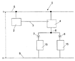
도 1은 열전 컴포넌트(thermoelectric component)(1)의 어셈블리를 위한 개별 컴포넌트들의 회로도를 도시한다. 트리거 유닛(trigger unit)(2)이 트리거 라인(3)을 통해 2개의 트랜지스터(4)들과 연결되고, 트리거 유닛(2)과 트랜지스터(4)들에는 전압원에 의해 양 전위(positive potential)(5)가 공급된다. 트리거 유닛(2)과 트랜지스터(4)는 제어 유닛의 부분이다. 트랜지스터(4)의 출력측에서, 라인(6)은 2개의 보호(protective) 다이오드(7, 8)들을 통과하여 냉각 엘리먼트(15)로 각각 분기한다. 냉각 엘리먼트(15)들은 열전 컴포넌트의 써멀 엘리먼트들 또는 냉각 섹션들이다. 예를 들어, 보호 다이오드(7, 8)들은 쇼트키 보호 다이오드로 구성될 수 있고, 전류 흐름을 냉각 엘리먼트(15)의 방향으로 유도할 수 있다. 두 냉각 엘리먼트(15)들은 일측의 제로 전위(zero potential)(9)와 연결되고, 타측의 2개의 보호 다이오드(7, 8)들을 통해 트랜지스터(4)들에 의해 전압이 인가된다.Fig. 1 shows a circuit diagram of the individual components for the assembly of a
전원 공급에 기인하여, 냉각 엘리먼트(15)들이 마이크로전자 컴포넌트들, 예를 들어 마이크로프로세서의 컴포넌트들의 냉각을 위한 냉각을 발생시키는 것이 달성된다. 이러한 이유로, 회로도의 모든 컴포넌트들이 집적회로에 부가적으로 통합되는 것이 의도된다. 이러한 통합은 도 4 내지 도 8의 실시예에 따라 적어도 한번, 바람직하게는 수차례 발생할 수 있다. 발생하는 냉각은 본질적으로 공지된 펠티어 효과(Peltier effect)에 기인한다. 펠티어 효과의 기초는 전도대들(conduction bands)의 상이한 에너지 준위를 가지는 두 소재들(materials), 특히 브리지 엘리먼트에 의해 전기적으로 연결되는 일측의 p-도핑 반도체 소재(p-doped semiconducting material) 및 타측의 n-도핑 반도체 소재의 접촉이다. 전기(electricity)가 차례로 배치되는 반도체 소재의 두 접촉점(contact points)을 통과할 때, 인접한 반도체 소재의 고에너지 전도대로 전자들(electrons)을 운반하기 위해 접촉점 중 하나에서 열 에너지가 흡수되어야 하므로, 냉각 효과가 발생한다. 다른 접촉점에서 전자들은 높은 에너지 레벨에서 낮은 에너지 레벨로 떨어지므로, 이 경우에 냉각은 전자들이 n-도핑 반도체에서 p-도핑 반도체로 전자들이 이동하는 지점에서 발생한다.Due to the power supply, it is achieved that the
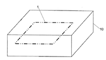
도 2는 집적회로(10)를 원근법의 개략도로 도시하고, 마이크로프로세서 또는 유사한 컴포넌트들의 구조가 통합된다. 예를 들어, 상당한 양의 열이 발생하는 등의 마이크로프로세서의 높은 전력 소비로 인하여, 완전한 집적회로(10)의 추가적인 냉각은 냉각 시스템 및 팬을 통해 발생할 뿐만 아니라 집적회로 내에서 추가적으로 필요하다. 따라서, 본 발명은 집적회로의 개별 층 사이에 배치되거나, 집적회로(10)의 최저 또는 최고 위치에 배치되는, 적어도 하나의 냉각 엘리먼트(15)를 갖는 적어도 하나의 부가적인 열전 컴포넌트(1)를 집적회로(10) 내에 통합하는 것을 제안한다. 하지만, 예를 들면, 상기 집적회로가 상응하는 제어 로직에 의해 일시적으로 스위칭 온 및 오프되는 수개의 병렬 실행 마이크로프로세서로 구성될 때, 이를테면 온도의 현저한 상승이 발생하고 부분적인 셧다운 또는, 필요하다면, 냉각이 요구되는 경우, 집적회로 내의 개별 컴포넌트들의 바로 아래에 수개의 열전 컴포넌트(1)들을 배치할 가능성도 있다. 따라서, 마이크로프로세서들이 집적회로(10) 내에 다중 배치로 통합되면, 각각의 개별 마이크로프로세서가 그런 열전 컴포넌트(1)에 할당될 수 있고, 그것은 간단한 구조를 특징으로 할 수 있지만, 도 4 내지 도 8에 따라 더 복잡하게 구조화될 수도 있다. 도 2는 단지 개략적인 도면에서 점선에 의해 열전 컴포넌트(1)의 하나의 위치를 도시하지만, 임의로 선택되었고 임의로 집적회로(10) 내에서 변경될 수 있다.FIG. 2 shows the
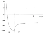
도 3은 냉각 엘리먼트(15)에 대한 통상적인 냉각 흐름의 온도-시간 다이어그램을 도시한다. 냉각 엘리먼트(15)의 온도는, 온도가 약 -15°의 값으로 추가로 안정화될 때까지, 0℃ 이상에서 -30℃ 이하의 온도로 강하한다. 극단적 냉각 온도의 장점을 이용하기 위해, 냉각 엘리먼트(15)에는 -30°의 온도에 도달하는 시점(x)까지의 활성 위상(active phase)에서 전압이 공급된다. 다음에, 냉각 엘리먼트(15)는 휴지 위상(resting phase)으로 이동되는 반면, 냉각 효과를 반복적으로 사용하기 위해, 다른 것 이후의 제2 또는 추가 냉각 엘리먼트(15)에 전력이 공급된다. 수개의 개별 냉각 엘리먼트(15)들을 사용함으로써, 활성 위상(16) 동안의 최대 온도 강하가 집적회로를 냉각시키는데 사용될 수 있는 반면, 냉각 엘리먼트(15)는 휴지 위상(17) 동안 주변 온도로 조정된다. 그런 방식으로 수개의 냉각 엘리먼트(15)들이 사용되는 한, -15℃ 이하의 냉각을 구현하기 위해 냉각 엘리먼트(15)의 온도 조정에도 불구하고 연속적인 냉각이 달성될 수 있다.Figure 3 shows a temperature-time diagram of a typical cooling flow for the
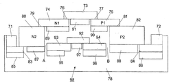
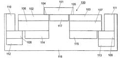
도 4는 현 상황에서 마이크로프로세서와 같은 집적회로 내에서 구현될, 적어도 하나의 냉각 엘리먼트(15)를 갖는 본 발명에 따른 열전 컴포넌트(1)의 어셈블리의 개략도를 도시한다. 도 4의 써멀 엘리먼트(29)들은 도 1의 냉각 엘리먼트(15)에 대응한다. 전압을 인가하기 위해서, 정상 환경에서 양의 전압이 공급되는 제1 접촉 영역(20)이 형성된다. 한편, 제2 접촉 영역(21)은 제로 전위(zero potential)에 접속되고, 제2 접촉 영역(21)은 냉각 엘리먼트(15)의 접촉(contacting)이 가능해지도록 치수화된다(dimensioned). 집적회로 내의 열전 컴포넌트(1)은 제로 전위에 대한 접촉부(contact)로서의 의미를 갖는 제1 접촉 영역(22)으로 구성되고, 냉각 섹션(27, 28, 30, 31, 32)들을 특징으로 한다. 전압 공급은 제1 접촉 영역(20)을 통해, 전력 공급을 위해 동시 또는 순차적으로 스위칭되어 기동(starting) 전류를 감소시키기 위해, 병렬로 스위칭되는 2개의 트랜지스터(24, 25)들에 의해 발생한다. 전류는 부가적인 회로 엘리먼트(26)를 통해 차단될 수 있다. 전류의 차단이 발생할 수 있는데, 집적회로의 일부가 영구적으로 비활성이거나 또는 목표된(targeted) 열전 컴포넌트(1)이 온도를 낮추기 위하여 집적회로 내의 온도 상승 중에 스위칭 온 될 수 있는 경우이다. 이러한 열전 컴포넌트(1) 내의 전류는 제1 접촉 영역(22), 냉각 섹션(27, 28, 30, 31, 32)들 및 제2 접촉 영역(23)을 통해 발생한다. 제1 접촉 영역(22)은 냉각 섹션을 통해 제2 접촉 영역(23)에 전기적으로 연결되고, 3개의 서로 다른 연결들이 도 4에 도시되어 있다.4 shows a schematic view of an assembly of a
제1 실시예에서, 제1 접촉 영역(22)은 등거리의 거리에 배치된 수개의 병렬 실행 냉각 섹션을 통해 제2 접촉 영역(23)에 연결될 수 있으며, 개별 냉각 섹션(27, 28)들은 써멀 엘리먼트(29)들로 구성된다. 냉각 섹션(27, 28)들이 등거리의 거리(equidistant distances)로 평행하게 진행될 때, 영역에 대한 일정한 온도의 냉각이 이루어진다. 부가적인 센서 엘리먼트(33)들이 개별 냉각 섹션(27, 28)들 사이에 배치될 수 있어, 제1 접촉 영역(22)으로의 전류 공급을 차단 또는 결합시키는 것과 같이, 현재 온도 기울기(gradients)에 의존하는 스위칭 프로세스를 트리거한다. 제1 접촉 영역(22), 제2 접촉 영역(23), 냉각 섹션(27, 28)들 및 써멀 엘리먼트(29)들은 서로의 위에 층들로 배치될 수 있다.The
대안적으로, 제1 냉각 섹션(28) 및 제2 냉각 섹션(30)이 존재하도록 각도(α)로 냉각 섹션들을 배치하는 가능성이 있으며, 주어진 각도 및 냉각 섹션(28, 30)들 사이의 가변하는 거리에 기인하여, 더 빠른 냉각이 제1 접촉 영역(22)의 근방에서 달성되는 반면, 현저하게 느린 냉각이 성장하는(growing) 거리로, 특히 제2 접촉 영역(23)의 근방에서 발생한다. 이러한 구성은 제2 실시예를 나타내며, 또한 다중 배치로 서로의 위에 층들로 배치될 수 있다.Alternatively, there is a possibility to place the cooling sections at an angle? Such that the
대안으로, 2개의 열전 냉각 섹션(31, 32)들을 통해 제1 접촉 영역(22)을 제2 접촉 영역(23)과 전기적으로 연결하는 가능성이 있다. 이 경우, 2개의 열전 냉각 섹션(31, 32)들의 주기적으로 변하는 거리에 기인하여, 가변 온도 강하가 달성된다. 이 실시예와 관련하여, 도 4의 제3 실시예가 도시된다. 제1 실시예에서와 같이, 온도 센서(33)들이 제2 및 제3 실시예에서 사용될 수 있고, 여기서 상기 온도 센서(33)는 제어 유닛을 통해 냉각 섹션(31, 32)들의 선택적 전압 공급을 허용한다.Alternatively, there is a possibility of electrically connecting the
도 5는 일반적으로 수개의 써멀 엘리먼트(29)들이 반도체 칩에서 서로 옆에 및/또는 서로 위에 배치될 수 있는 층 배치(layered arrangement)의 써멀 엘리먼트(29)의 개략도를 도시한다. 여기서, 한편으로는 펠티어 효과를 사용하고, 수개의 써멀 엘리먼트(29)들을 통해 집적회로의 영역을 의도적으로 냉각시키기 위해, 직렬 또는 병렬로 개별 써멀 엘리먼트(20)를 전기적으로 실행하는 추가의 가능성이 존재한다.Fig. 5 shows a schematic view of a layered arrangement of
2개의 전기적 접촉 영역(50, 51)들로, 개별 써멀 엘리먼트(29)를 추가의 써멀 엘리먼트(29)들과 병렬 또는 직렬로 연결하거나 전압 공급을 위해 상기 접촉 영역(50, 51)들을 사용하는 가능성이 있다. 여기서, 전체 배치는 기판(52) 내에 임베디드(embedded) 되는데, 기판(52)은 복수의 유사한 써멀 엘리먼트(29)들을 유지할 수 있고, 예를 들어 마이크로프로세의 개별 마이크로전자 컴포넌트들을 추가로 유지할 수 있어, 목표된 냉각이 많은 열을 방출하는 영역들에서 발생할 수 있도록 마이크로프로세서의 구조에 대한 써멀 엘리먼트(29)들의 직접 할당이 의도될 수 있다.It is also possible to connect the individual
써멀 엘리먼트(29)는 접촉 영역(54, 55)을 통해 p-도핑 또는 n-도핑 반도체 소재에 연결되는 제1 상부 브리지 엘리먼트(53)의 2개의 접촉 영역(50, 51)에 추가로 구성된다. p-도핑 반도체 소재(56)는 하부 브리지 엘리먼트(58)를 통해 제1 접촉 영역(50)과 전기적으로 접속되는 반면, n-도핑 반도체 소재(57)는 제2 하부 브리지 엘리먼트(59)를 통해 제2 전기적 접촉 영역(51)에 접속된다. 전류의 방향에 의존하여, 반도체 소재(56, 57)들의 역방향(reverse) 도핑이 발생할 수 있다. 써멀 엘리먼트(29)의 각각의 개별 컴포넌트는 접착층(60, 61, 62, 63, 64)을 통해 기판(52)에 연결된다.The
또한, 써멀 엘리먼트(29)의 이러한 기본적인 배치는 독특한 특징을 나타내는데, 즉 두 도핑 반도체 소재들(56,57)이 다른 치수를 갖는 접촉 영역(54, 55)들을 통해 상부 브리지 엘리먼트(53)와 연결되어, 도핑 반도체 소재(56, 57)들의 형태를 채용할 필요없다. 접촉 영역(54, 55)들은 반도체 소재(56, 57)들이 상부 브리지(53)에 대해 정렬되지 않게 배치됨으로써 이미 변경될 수 있다. 여기서, 접촉 영역(54, 55)들이 커질수록, 열 수송이 작아지는 룰(rule)이 적용된다. 열 소산은 제1 도핑 반도체 소재(56)의 노출 영역(65, 66)들 또는 제2 도핑 반도체 소재(57)의 각각의 영역(67, 68)들을 통해 발생한다. 이러한 써멀 엘리먼트(29)의 간단한 구조는 또한 추가의 더 복잡한 실시예들에 대한 기초가 된다.This basic arrangement of the
도 6은 개략도로 수개의 써멀 엘리먼트(29)들로 구성되는 열전 냉각 어레이(70)의 어셈블리를 도시한다. 또한, 냉각 어레이(70)는, 서로 다른 냉각 어레이(70)들을 서로 연결하거나 또는 전압 공급을 위해 사용되는 제1 접촉 영역(71) 및 제2 접촉 영역(72)을 특징으로 한다. 제1 n-도핑 반도체 소재(74) 및 제2 p-도핑 반도체 소재(75)는 상부 브리지 엘리먼트(73)를 통해 연결되고, 상기 연결은 상이한 크기의 접촉 영역(76, 77)들을 통해 발생한다. 이에 대한 배경은, 통과 전류를 고려할 때 작은 접촉 영역(76)은 예를 들어 기판(78)으로부터 방출되는 것보다 많은 열을 방출하는 반면, 큰 접촉 영역(77)은 기판 (78) 내로 더 적은 열을 방출한다는 것이다. 제1 n-도핑 반도체 소재는 접촉 영역(79)을 통해 제2 n-도핑 반도체 소재(80)에 추가로 연결되는 반면, p-도핑 반도체 소재(75)는 접촉 영역(81)을 통해 추가의 p-도핑 반도체 소재(82)에 연결된다. 두 개의 계단식(step-lined) n-도핑 또는 p-도핑 반도체 소재(74, 75, 80, 82)들에 기인하여, 더 높은 냉각 용량이 달성된다.FIG. 6 shows an assembly of a thermoelectric cooling array 70 that is schematically composed of several
제1 p-도핑 반도체 소재(74, 75)들(예를 들어, Bi2Te3, BN, TiN, SiGeN, PbTeN)가 기재(base material)로서 사용되며, 동일한 소재들이 제2 n-도핑 반도체 소재(80, 82)들에 대한 기재로서 사용될 수 있다. 일반적으로, p-도핑 반도체 소재 및 n-도핑 반도체 소재에 사용될 기재는 집적회로 냉각 어레이의 작동 온도에 의존한다. 제2 n-도핑 반도체 소재(80, 82)는 도전층을 통한 전류 흐름이 달성될 수 있도록 하부 브리지 엘리먼트(83, 84)를 통해 제1 접촉 영역(71) 또는 제2 접촉 영역(72)과 각각 다시 연결된다. 하부 브리지 엘리먼트(83, 84)들은 접착층(87, 88)을 통해 기판(78)과 연결되는 반면, 제1 도핑 반도체 소재(74, 75)들은 접착층(89, 90)을 통해 연결되며, 상부 브리지 엘리먼트(73)는 접착층(91)을 통해 기판(79)과 연결된다. 여기에 도시된 대안은 부가적으로 제1 p-도핑 반도체 소재(93)와 제2 n-도핑 반도체 소재(94)를 연결하고, 다시 접착층(95, 96, 97)들을 통해 기판(78)과 연결되는 추가의 브리지 엘리먼트(92)를 특징으로 한다. 이러한 제3 도핑 반도체 소재(93, 94)들의 직접적인 전기적 접촉은, 다른 배치와 대조적으로, 사용할 수 없다. 제3 반도체 소재들(93, 94)들은 유전체인 기판(78) 내에 임베디드 된다. 제2 도핑 반도체 소재(80)와 제3 도핑 반도체 소재(93) 사이의 거리(A)와 제2 도핑 반도체 소재(82)와 제3 도핑 반도체 소재(94) 사이의 거리(B)는 동일하지 않도록 선택되었지만, 매우 작게 유지되어, 기판(78)은 -30° 부근의 온도에 대해 이런 짧은 거리에 대해 전도성이 되고, 따라서 부가적인 써멀 엘리먼트(98)의 전압 공급이 발생한다. 이러한 방식으로 달성될 수 있는데, 온도의 후속 상승(subsequent rise)의 얻어지는 효과에도, 추가의 냉각에 기인하여, 약 -30°의 냉각으로, 약 -30°의 온도가 오랜 시간 동안 유지될 수 있다는 것이 달성될 수 있다.The first p-doped
도 7은 제벡 효과(Seebeck effect)에 따른 열전 발생기(100)의 개략적인 배치를 도시한다. 열전 발생기(100)는 접촉 영역(104, 105)을 통해 제1 n-도핑 반도체 소재 (102) 및 제1 p-도핑 반도체 소재(103)에 연결되는 상부 브리지 엘리먼트(101)로 구성된다. 제1 도핑 반도체 소재(102, 103)들은 제2 n-도핑 반도체 소재(106) 및 제2 p-도핑 반도체 소재(107)에 연결된다. 이 경우에, 제1 반도체 소재(102, 103)들 및 각각의 제2 반도체 소재(106, 107)들은 완전히 접촉한다. 제2 반도체 소재(106, 107)들은 하부 브리지 엘리먼트(108)를 통해 제1 접촉 영역(110) 및 제2 접촉 영역(111)과 연결된다. 접촉 영역(110, 111)들은 다시 개별적인 열전 발생기 엘리먼트(100)들을 연결하거나 전압을 입력하기 위해 사용된다. 하부 브리지 엘리먼트(108 및 109)들은 접착층(112, 113)을 통해 기판(116)과 연결되고 제2 도핑 반도체 소재(106, 107)들은 접착층(114, 115)을 통해 기판(116)과 연결되는 반면, 상부 브리지 엘리먼트(101)는 접착층(117)을 통해 기판(116)과 연결된다.FIG. 7 shows a schematic arrangement of the
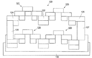
도 8은 서로 냉각 어레이(120)를 형성하도록 설정되는 써멀 엘리먼트들의 다중 배치를 개략도로 도시한다. 제1 써멀 엘리먼트(121)는 제2 써멀 엘리먼트(123)와 연결되어, 브리지 엘리먼트(122)를 통해 연결된다. 각각의 개별 써멀 엘리먼트(121, 123)의 어셈블리는 도 4에 따른 써멀 엘리먼트의 어셈블리에 대응한다. 전압 공급은 제1 접촉 영역(124) 및 제2 접촉 영역(125)을 통해 발생한다. 두 접촉 영역(124, 125)들은 써멀 엘리먼트의 4중 배치가 사용가능하도록 유전체 화합물 층(126, 127)을 통해 2개의 추가 써멀 엘리먼트(128, 129)와 연결된다. 이런 경우에, 2개의 상부 써멀 엘리먼트(121, 123)들은 2개의 하부 써멀 엘리먼트(128, 129)들과 마찬가지로 직렬로 스위칭된다. 또한, 상부 써멀 엘리먼트(121, 123)들은 전기적 화합물 층(126, 127)을 통해 하부 써멀 엘리먼트(128, 129)들과 병렬로 스위칭되므로, 임의의 써멀 엘리먼트(121, 123, 128, 129)들이 활성화 가능하다. 이러한 배치의 장점은 하부 배치의 써멀 엘리먼트(128, 129)들이 대응하는 냉각을 통해서만 스위칭 온되어, 지연 연결에 기인하여 더 낮은 시동 전류가 발생한다는 것이다.8 schematically illustrates multiple arrangements of thermal elements that are configured to form a
4개의 모든 써멀 엘리먼트(121, 123, 128, 129)들은 기판(130)에 통합되고, 각각 접착층들을 통해 기판(130)과 연결된다.All four
이 경우에, 열전기 발생기(100)는 집적회로에 의해 생성된 폐열(waste heat)에 기인하여 추가적인 전압 발생을 위해 사용되어야 한다. 생성된 폐열은 제벡 효과에 기인하여 열전 발생기(100)에서의 전압 발생을 초래하며, 써멀 엘리먼트들의 공급을 위해 집적회로 내에서 사용될 수 있다. 따라서, 이러한 열전 발생기(100)는 바람직하게 얻어지는 폐열을 사용하기 위해 집적회로의 상부 층에 바람직하게 사용될 수 있다.In this case, the
1 : 열전 컴포넌트
2 : 트리거 유닛
3 : 트리거 라인
4 : 트랜지스터
5 : 양 전위
6 : 라인
7 : 보호 다이오드
8 : 보호 다이오드
9 : 제로 전위
10 : 집적회로
15 : 냉각 엘리먼트
16 : 활성 위상(active phase)
17 : 휴지 위상(rest phase)
20 : 제1 접촉 영역
21 : 제2 접촉 영역
22 : 제1 접촉 영역
23 : 제2 접촉 영역
24 : 트랜지스터
25 : 트랜지스터
26 : 회로 엘리먼트
27 : 냉각 섹션
28 : 냉각 섹션
29 : 써멀 엘리먼트(thermal element)
30 : 냉각 섹션
31 : 냉각 섹션
32 : 냉각 섹션
33 : 센서
50 : 접촉 영역
51 : 접촉 영역
52 : 기판
53 : 브리지 엘리먼트
54 : 접촉 영역
55 : 접촉 영역
56 : 반도체 소재
57 : 반도체 소재
58 : 브리지 엘리먼트
59 : 브리지 엘리먼트
60 : 접착층
61 : 접착층
62 : 접착층
63 : 접착층
64 : 접착층
65 : 영역
66 : 영역
67 : 영역
68 : 영역
70 : 냉각 어레이
71 : 접촉 영역
72 : 접촉 영역
73 : 브리지 엘리먼트
74 : 반도체 소재
75 : 반도체 소재
76 : 접촉 영역
77 : 접촉 영역
78 : 기판
79 : 접촉 영역
80 : 반도체 소재
81 : 접촉 영역
82 : 반도체 소재
83 : 브리지 엘리먼트
84 : 브리지 엘리먼트
85 : 접착층
86 : 접착층
87 : 접착층
88 : 접착층
89 : 접착층
90 : 접착층
91 : 접착층
92 : 브리지 엘리먼트
93 : 반도체 소재
94 : 반도체 소재
95 : 접착층
96 : 접착층
97 : 접착층
98 : 써멀 엘리먼트
100 : 열전 발생기
101 : 브리지 엘리먼트
102 : 반도체 소재
103 : 반도체 소재
104 : 접촉 영역
105 : 접촉 영역
106 : 반도체 소재
107 : 반도체 소재
108 : 브리지 엘리먼트
109 : 브리지 엘리먼트
110 : 접촉 영역
111 : 접촉 영역
112 : 접착층
113 : 접착층
114 : 접착층
115 : 접착층
116 : 기판
117 : 접착층
120 : 냉각 섹션
121 : 써멀 엘리먼트
122 : 브리지 엘리먼트
123 : 써멀 엘리먼트
124 : 접촉 영역
125 : 접촉 영역
126 : 화합물 층
127 : 화합물 층
128 : 써멀 엘리먼트
129 : 써멀 엘리먼트
130 : 기판
A : 거리
B : 거리1: thermoelectric component 2: trigger unit
3: Trigger line 4: Transistor
5: positive potential 6: line
7: Protection diode 8: Protection diode
9: Zero potential 10: Integrated circuit
15: cooling element 16: active phase
17: rest phase 20: first contact area
21: second contact area 22: first contact area
23: second contact region 24: transistor
25: transistor 26: circuit element
27: cooling section 28: cooling section
29: thermal element 30: cooling section
31: cooling section 32: cooling section
33: sensor 50: contact area
51: contact area 52: substrate
53: bridge element 54: contact area
55: contact area 56: semiconductor material
57: semiconductor material 58: bridge element
59: bridge element 60: adhesive layer
61: Adhesive layer 62: Adhesive layer
63: adhesive layer 64: adhesive layer
65: area 66: area
67: area 68: area
70: cooling array 71: contact area
72: contact area 73: bridge element
74: Semiconductor material 75: Semiconductor material
76: contact area 77: contact area
78: substrate 79: contact area
80: Semiconductor material 81: Contact area
82: semiconductor material 83: bridge element
84: bridge element 85: adhesive layer
86: Adhesive layer 87: Adhesive layer
88: adhesive layer 89: adhesive layer
90: Adhesive layer 91: Adhesive layer
92: bridge element 93: semiconductor material
94: Semiconductor material 95: Adhesive layer
96: Adhesive layer 97: Adhesive layer
98: thermal element 100: thermoelectric generator
101: bridge element 102: semiconductor material
103: Semiconductor material 104: Contact area
105: contact area 106: semiconductor material
107: semiconductor material 108: bridge element
109: bridge element 110: contact area
111: contact area 112: adhesive layer
113: Adhesive layer 114: Adhesive layer
115: adhesive layer 116: substrate
117: adhesive layer 120: cooling section
121: thermal element 122: bridge element
123: thermal element 124: contact area
125: contact area 126: compound layer
127: compound layer 128: thermal element
129: thermal element 130: substrate
A: Distance B: Distance
Claims (29)
상기 열전 컴포넌트는 적어도 하나의 제1 접촉 영역(contact area)(22), 적어도 하나의 제2 접촉 영역(23) 및 적어도 하나의 냉각 섹션(cooling section)(27, 28, 30, 31, 32)을 포함하고,
상기 냉각 섹션(27, 28, 30, 31, 32)은 제1 접촉 영역(22)과 제2 접촉 영역(23) 사이에 배치되어, 제어 유닛을 통해 제1 접촉 영역(22)과 제2 접촉 영역(23)에 의해 전압이 공급되는 적어도 하나의 써멀 엘리먼트(thermal element)(29)로 구성되며,
상기 써멀 엘리먼트(29)는 브리지 엘리먼트(53, 58, 59, 73, 83, 84, 92)에 의해 연결되는 방식으로 되는 적어도 하나의 제1 도핑 층 및 적어도 하나의 제2 도핑 층으로 구성되고, 브리지 엘리먼트(53, 58, 59, 73, 83, 84, 92)는 제1 도핑 층 및/또는 제2 도핑 층 위에만 부분적으로 놓이는 것을 특징으로 하는 집적회로 냉각 어레이.
For a microprocessor or cooling device, preferably consisting of a dielectric substrate with a doped and distinguished area for the implementation of at least one thermoelectric component 1 forming a cooling array, In a circuit cooling array,
The thermoelectric component comprises at least one first contact area 22, at least one second contact area 23 and at least one cooling section 27, 28, 30, 31, 32, / RTI >
The cooling section 27, 28, 30, 31, 32 is disposed between the first contact area 22 and the second contact area 23, At least one thermal element (29) to which a voltage is supplied by the region (23)
The thermal element 29 is composed of at least one first doping layer and at least one second doping layer in a manner connected by the bridge elements 53, 58, 59, 73, 83, 84, 92, Wherein the bridge elements (53, 58, 59, 73, 83, 84, 92) are partially located only over the first doping layer and / or the second doping layer.
제1 도핑 층 또는 제2 도핑 층 위에 놓이는 브리지 엘리먼트(53, 58, 59, 73, 83, 84, 92)의 섹션 길이(x), 제1 도핑 층 또는 제2 도핑 층의 길이(y) 및 제1 도핑 층 또는 제2 도핑 층의 폭(z)은 0.2 < x/y < 0.5 및 z > x의 조건을 따르는 것을 특징으로 하는 집적회로 냉각 어레이.
The method according to claim 1,
(X) of the bridge elements (53, 58, 59, 73, 83, 84, 92) overlying the first doping layer or the second doping layer, the length (y) of the first doping layer or the second doping layer, Wherein the width (z) of the first doping layer or the second doping layer conforms to the condition of 0.2 < x / y < 0.5 and z> x.
냉각 섹션(27, 28, 30, 31, 32)은 제1 접촉 영역(22)과 제2 접촉 영역(23) 사이에 직렬로 각각 연결되는 수개의 써멀 엘리먼트(29)들로 이루어지고, 및/또는
냉각 섹션(27, 28, 30, 31, 32)은 제1 접촉 영역(22)과 제2 접촉 영역(23) 사이에 직렬로 각각 연결되는 수개의 써멀 엘리먼트(29)들로 이루어지고, 부가적인 써멀 엘리먼트(29)들이 개별 써멀 엘리먼트(29)들과 적어도 부분적으로 병렬로 연결되는 것을 특징으로 하는 집적회로 냉각 어레이.
3. The method according to claim 1 or 2,
The cooling sections 27, 28, 30, 31 and 32 comprise several thermal elements 29 connected in series between the first contact area 22 and the second contact area 23, respectively, and / or
The cooling sections 27, 28, 30, 31 and 32 are made up of several thermal elements 29 connected in series between the first contact area 22 and the second contact area 23 respectively, Characterized in that the thermal elements (29) are connected at least partially in parallel with the individual thermal elements (29).
브리지 엘리먼트와 제1 및 제2 도핑 층 사이의 접촉 영역(50, 51, 54, 55, 71 , 72, 76, 77, 79, 81)들은 크기 면에서 서로 다른 것을 특징으로 하는 집적회로 냉각 어레이.
The method according to claim 1, 2, or 3,
Wherein the contact areas (50, 51, 54, 55, 71, 72, 76, 77, 79, 81) between the bridge element and the first and second doping layers are different in size.
열전 컴포넌트(1)는 기판(52, 78) 위에 또는 기판(52, 78) 내에 배치되는 것을 특징으로 하는 집적회로 냉각 어레이.
5. The method according to any one of claims 1 to 4,
Wherein the thermoelectric component (1) is disposed on the substrate (52, 78) or within the substrate (52, 78).
수개의 열전 컴포넌트(1)들이 서로 옆에 및/또는 기판 내에서 서로 위에 배치되고, 및/또는
수개의 인접하는 열전 컴포넌트(1)들이 기판(52, 78) 위에 배치되는 것을 특징으로 하는 집적회로 냉각 어레이.
6. The method according to any one of claims 1 to 5,
Several thermoelectric components 1 are placed next to each other and / or on top of each other in the substrate, and / or
Wherein a plurality of adjacent thermoelectric components (1) are disposed on the substrate (52, 78).
수개의 열전 컴포넌트(1)들이 서로 위에 배치되고, 적어도 하나의 영구 또는 스위칭 가능한 VIA-연결부(수직 상호연결 접속: Vertical Interconnect Access)에 의해 연결되며, VIA-연결부의 스위칭은 제어 유닛을 통해 발생하는 것을 특징으로 하는 집적회로 냉각 어레이.
7. The method according to any one of claims 1 to 6,
Several thermoelectric components 1 are placed on top of each other and are connected by at least one permanent or switchable VIA connection (Vertical Interconnect Access), and the switching of the VIA connection occurs via a control unit Wherein the integrated circuit cooling array comprises:
수개의 냉각 섹션(27, 28, 30, 31, 32)들이 제1 접촉 영역(22)과 제2 접촉 영역(23) 사이에 병렬로 배치되는 것을 특징으로 하는 집적회로 냉각 어레이.
8. The method according to any one of claims 1 to 7,
Characterized in that several cooling sections (27, 28, 30, 31, 32) are arranged in parallel between the first contact area (22) and the second contact area (23).
각각의 냉각 섹션(27, 28, 30, 31, 32)은 다른 냉각 섹션들과 독립적으로 전압이 공급되는 것을 특징으로 하는 집적회로 냉각 어레이.
9. The method according to any one of claims 1 to 8,
Characterized in that each cooling section (27, 28, 30, 31, 32) is supplied with voltage independently of the other cooling sections.
서로 수평각(horizontal angle)(α)으로 진행하는 적어도 2개의 냉각 섹션((27, 28, 30, 31, 32)들이 존재하거나 또는 서로 주기적으로 교번하는 거리(periodically alternating distance)로 진행하는 적어도 2개의 냉각 섹션들이 존재하는 것을 특징으로 하는 집적회로 냉각 어레이.
10. The method according to any one of claims 1 to 9,
There is at least two cooling sections 27, 28, 30, 31, 32 running at a horizontal angle alpha to each other or at least two cooling sections 27, 28, 30, 31, 32 proceeding at periodically alternating distances from each other Wherein cooling sections are present.
냉각 섹션(27, 28, 30, 31, 32)의 2개의 써멀 엘리먼트(29)들 사이 또는 2개의 냉각 섹션(27, 28, 30, 31, 32)들 사이 또는 2개의 냉각 섹션(27, 28, 30, 31, 32)들의 2개의 세그먼트들 사이의 수평각은 5° 내지 85°, 바람직하게는 30°내지 40°, 특히 바람직하게는 10° 내지 20°사이인 것을 특징으로 하는 집적회로 냉각 어레이.
11. The method according to any one of claims 1 to 10,
It is possible to reduce the number of cooling elements 27, 28, 30, 31, 32 between the two thermal elements 29 of the cooling sections 27, 28, 30, 31, 32 or between the two cooling sections 27, , 30, 31, 32) is between 5 ° and 85 °, preferably between 30 ° and 40 °, particularly preferably between 10 ° and 20 °. .
열전 컴포넌트(1)의 수개의 써멀 엘리먼트(29)들 또는 냉각 섹션(27, 28, 30, 31, 32)들은 기판(52, 78) 내에서 서로 위에 배치되는 것을 특징으로 하는 집적회로 냉각 어레이.
12. The method according to any one of claims 1 to 11,
Wherein several thermal elements (29) or cooling sections (27, 28, 30, 31, 32) of the thermoelectric component (1) are disposed on top of each other within the substrate (52, 78).
제1 접촉 영역(22)과 수개의 제2 접촉 영역(23)들이 존재하고, 적어도 하나의 냉각 섹션(27, 28, 30, 31, 32)은 각각 제1 접촉 영역(22)과 수개의 제2 접촉 영역(23)들 사이에 배치되고, 및/또는 제1 접촉 영역(22)은 수개의 제2 접촉 영역(23)들에 의해 둘러싸이고, 적어도 하나의 냉각 섹션(27, 28, 30, 31, 32)은 각각 제1 접촉 영역(22)과 제2 접촉 영역(23)들 사이에 배치되는 것을 특징으로 하는 집적회로 냉각 어레이.
13. The method according to any one of claims 1 to 12,
There is a first contact area 22 and a number of second contact areas 23 and at least one cooling section 27, 28, 30, 31, 32 has a first contact area 22, 2, and / or the first contact area 22 is surrounded by several second contact areas 23, and at least one cooling section 27, 28, 30, 31, 32) are disposed between the first contact area (22) and the second contact area (23), respectively.
수개의 냉각 섹션(27, 28, 30, 31, 32)들은 제1 접촉 영역(22)으로부터 스타 구조의 형태로 제1 접촉 영역(22)을 둘러싸는 제2 접촉 영역(23)으로 또는 제1 접촉 영역(22)을 둘러싸는 수개의 제2 접촉 영역(23)들로 연장하는 것을 특징으로 하는 집적회로 냉각 어레이.
14. The method according to any one of claims 1 to 13,
The plurality of cooling sections 27, 28, 30, 31 and 32 extend from the first contact area 22 into the second contact area 23 surrounding the first contact area 22 in the form of a star structure, Extends to a number of second contact areas (23) surrounding the contact area (22).
온도 센서(33)들이 제어 유닛과 상호 작용하는 적어도 2개의 냉각 섹션(27, 28, 30, 31, 32)들 사이에 배치되는 것을 특징으로 하는 집적회로 냉각 어레이.
15. The method according to any one of claims 1 to 14,
Characterized in that the temperature sensors (33) are arranged between at least two cooling sections (27, 28, 30, 31, 32) interacting with the control unit.
제어 유닛은 수개의 열전 컴포넌트(1)들 중 하나 또는 수개의 냉각 섹션(27, 28, 30, 31, 32)들 중 하나의 선택적인 전압 공급을 위한 회로 엘리먼트를 포함하는 것을 특징으로 하는 집적회로 냉각 어레이.
16. The method according to any one of claims 1 to 15,
Characterized in that the control unit comprises circuit elements for the selective voltage supply of one of the several thermoelectric components (1) or one of several cooling sections (27, 28, 30, 31, 32) Cooling array.
제어 유닛은 블로킹(blocking) 다이오드를 통해 열전 컴포넌트에 전압을 공급하는 트랜지스터(24, 25)를 포함하거나, 또는 제어 유닛은 병렬로 연결되고 각각 다른 열전 컴포넌트(1)들과 관련하여 동시에 또는 시차 간격(staggered intervals)으로 블로킹 다이오드를 통해 열전 컴포넌트에 전압을 공급하는 수개의 트랜지스터(24, 25)들을 포함하는 것을 특징으로 하는 집적회로 냉각 어레이.
12. The method according to any one of claims 1 to 11,
The control unit includes transistors (24, 25) for supplying a voltage to the thermoelectric component via a blocking diode, or the control unit may be connected in parallel and at the same time with respect to the different thermoelectric components (1) and a plurality of transistors (24, 25) for supplying a voltage to the thermoelectric component via a blocking diode at staggered intervals.
제어 유닛은 서로 독립적으로 기존의 스위칭 가능한(existing switchable) VIA-연결부들을 스위칭하는 것을 특징으로 하는 집적회로 냉각 어레이.
18. The method according to any one of claims 1 to 17,
And the control unit switches existing existing switchable VIA-connections independently of each other.
제어 유닛은 고주파 펄스 발생기 및 상기 고주파 펄스 발생기에 의해 트리거 될 수 있는 카운팅 유닛을 갖는 프로그램 가능한 디바이스를 포함하며, 적어도 2개의 열전 컴포넌트(1)들 사이의 VIA-연결부는 카운팅 유닛의 카운터 값과 관련하여 제어 유닛에 의해 스위칭되는 것을 특징으로 하는 집적회로 냉각 어레이.
19. The method according to any one of claims 1 to 18,
The control unit includes a programmable device having a high frequency pulse generator and a counting unit that can be triggered by the high frequency pulse generator, wherein the VIA-connection between at least two thermoelectric components (1) is associated with a counter value of the counting unit And switched by the control unit.
써멀 엘리먼트(29)의 제1 도핑 층은 n-도핑 층이며, 써멀 엘리먼트(29)의 제2 도핑 층은 p-도핑 층인 것을 특징으로 하는 집적회로 냉각 어레이.
20. The method according to any one of claims 1 to 19,
Wherein the first doping layer of the thermal element (29) is an n-doped layer and the second doping layer of the thermal element (29) is a p-doped layer.
브리지 엘리먼트(53, 58, 59, 73, 83, 84, 92)는 고도의 폴리실리콘(highly polysilicon), 금속 또는 금속 합금으로 이루어지는 것을 특징으로 하는 집적회로 냉각 어레이.
21. The method according to any one of claims 1 to 20,
Characterized in that the bridge elements (53, 58, 59, 73, 83, 84, 92) are made of highly polysilicon, metal or metal alloy.
열전 컴포넌트(1)의 더 따뜻한(warmer) 측에 접하도록 배치되는, 적어도 하나의 차폐(shielding) 층이 존재하는 것을 특징으로 하는 집적회로 냉각 어레이.
22. The method according to any one of claims 1 to 21,
Characterized in that there is at least one shielding layer arranged to contact the warmer side of the thermoelectric component (1).
차폐 층은 전기적 절연 소재를 포함하며, 상기 절연 소재는 높은-k 및/또는 낮은-k 유전체 매체(dielectric medium), 특히 실리콘 디옥사이드, AgO, Ti02, HfO2 또는 Al2O3로 이루어지는 것을 특징으로 하는 집적회로 냉각 어레이.
23. The method according to any one of claims 1 to 22,
The shielding layer comprises an electrically insulating material, which is characterized by being comprised of a high-k and / or low-k dielectric medium, in particular silicon dioxide, AgO, TiO 2 , HfO 2 or Al 2 O 3 Lt; / RTI >
열 전도성 소재로 이루어지는, 열전 컴포넌트(1)의 더 차가운(cooler) 측의 적어도 하나의 브리지 엘리먼트(53, 58, 59, 73, 83, 84, 92)와 접촉하는, 적어도 하나의 냉각 층이 존재하는 것을 특징으로 하는 집적회로 냉각 어레이.
24. The method according to any one of claims 1 to 23,
There is at least one cooling layer in contact with at least one bridge element (53, 58, 59, 73, 83, 84, 92) on the cooler side of the thermoelectric component (1) Wherein the integrated circuit is an integrated circuit.
집적 회로는 적어도 하나의 기능 유닛(functional unit)을 포함하며, 상기 기능 유닛은 열전 컴포넌트(1) 사이 및/또는 열전 컴포넌트(1)의 냉각 섹션(27, 28, 30, 31, 32)들 사이에 배치되거나 및/또는 냉각 섹션(27, 28, 30, 31, 32)의 더 따뜻한(warmer) 또는 더 차가운(cooler) 측에 배치되는 것을 특징으로 하는 집적회로 냉각 어레이.
25. The method according to any one of claims 1 to 24,
The integrated circuit comprises at least one functional unit which is arranged between the thermoelectric components 1 and / or between the cooling sections 27, 28, 30, 31, 32 of the thermoelectric component 1, And / or arranged on a warmer or cooler side of the cooling section (27, 28, 30, 31, 32).
기능 유닛은,
- 센서, 특히 열 센서 또는 광학 센서,
- 정류기, 특히 다이오드,
- 스위칭 엘리먼트, 특히 트랜지스터, 바람직하게는 IGFET, NMOS, PMOS, VMOS와 같은 MOSFET,
- 제어 엘리먼트,
- 프로그램 가능한 디바이스, 특히 마이크로프로세서, 마이크로컨트롤러 또는 FPGA 또는 PLD와 같은 프로그램 가능한 로직,
- DRAM, ROM, SRAM과 같은 메모리 엘리먼트,
- 태양 전지판,
- 레이저 다이오드,
- 발광 다이오드 또는
- 마이크로 스트립(micro strip)을 포함하는 것을 특징으로 하는 집적회로 냉각 어레이.
26. The method according to any one of claims 1 to 25,
The functional unit,
Sensors, in particular thermal or optical sensors,
- rectifiers, especially diodes,
Switching elements, in particular transistors, preferably MOSFETs such as IGFET, NMOS, PMOS, VMOS,
- control element,
Programmable devices, in particular microprocessors, microcontrollers or programmable logic such as an FPGA or PLD,
Memory elements such as DRAM, ROM, SRAM,
- Solar panels,
- Laser diode,
- Light emitting diodes or
- a micro strip. ≪ RTI ID = 0.0 > - < / RTI >
열전 컴포넌트(1)는 기판(52, 78) 위에 또는 기판(52, 78)의 상부 층 중 하나에 배치되고, 마이크로전자 컴포넌트들의 폐열이 전압을 발생시키는데 사용되는 것을 특징으로 하는 집적회로 냉각 어레이.
27. The method according to any one of claims 1 to 26,
The thermoelectric component 1 is disposed on a substrate 52, 78 or in one of the upper layers of the substrate 52, 78, and the waste heat of the microelectronic components is used to generate a voltage.
집적 회로는 0.5 pA 내지 500 mA, 특히 1 mA 내지 200 mA, 바람직하게는 20 μA 내지 120 μA, 특히 바람직하게는 10 pA 내지 1 μA의 총 전류(total electric currents)에 대해 설계되는 것을 특징으로 하는 집적회로 냉각 어레이.
28. The method according to any one of claims 1 to 27,
The integrated circuit is designed for total electric currents of 0.5 pA to 500 mA, especially 1 mA to 200 mA, preferably 20 to 120 μA, particularly preferably 10 pA to 1 μA Integrated circuit cooling array.
중간층(intermediate layer)이 기판(52, 78) 내에서 서로 위에 배치되는 열전 컴포넌트(1)들 사이에 배치되어, 열전 컴포넌트(1)들 사이의 거리를 결정하는 것을 특징으로 하는 집적회로 냉각 어레이.29. The method according to any one of claims 1 to 28,
An intermediate layer is disposed between thermoelectric components (1) disposed on top of each other in a substrate (52, 78) to determine the distance between thermoelectric components (1).
Applications Claiming Priority (3)
| Application Number | Priority Date | Filing Date | Title |
|---|---|---|---|
| PCT/EP2014/061335 WO2015185082A1 (en) | 2014-06-02 | 2014-06-02 | Integrated, three-dimensional cell configuration, integrated cooling array and cell-based integrated circuit |
| EPPCT/EP2014/061335 | 2014-06-02 | ||
| PCT/EP2015/001109 WO2015185204A1 (en) | 2014-06-02 | 2015-06-01 | Integrated circuit with cooling array |
Publications (1)
| Publication Number | Publication Date |
|---|---|
| KR20170013331A true KR20170013331A (en) | 2017-02-06 |
Family
ID=50897581
Family Applications (1)
| Application Number | Title | Priority Date | Filing Date |
|---|---|---|---|
| KR1020167036633A KR20170013331A (en) | 2014-06-02 | 2015-06-01 | Integrated circuit with cooling array |
Country Status (17)
| Country | Link |
|---|---|
| US (1) | US20180145241A1 (en) |
| EP (1) | EP3149785A1 (en) |
| JP (2) | JP2017525133A (en) |
| KR (1) | KR20170013331A (en) |
| CN (2) | CN106463606A (en) |
| AP (1) | AP2017009669A0 (en) |
| AU (1) | AU2015271243A1 (en) |
| BR (1) | BR112016028369A2 (en) |
| CA (2) | CA2949931A1 (en) |
| EA (1) | EA201650136A1 (en) |
| IL (2) | IL249179A0 (en) |
| MA (1) | MA40285A (en) |
| MX (1) | MX365124B (en) |
| SG (3) | SG11201609840XA (en) |
| TR (1) | TR201700279T1 (en) |
| WO (2) | WO2015185082A1 (en) |
| ZA (1) | ZA201608808B (en) |
Families Citing this family (5)
| Publication number | Priority date | Publication date | Assignee | Title |
|---|---|---|---|---|
| CN106655893A (en) * | 2016-12-25 | 2017-05-10 | 北京工业大学 | Module in chip and used for converting heat energy into electric energy |
| US10586138B2 (en) * | 2017-11-02 | 2020-03-10 | International Business Machines Corporation | Dynamic thermoelectric quick response code branding |
| US10430620B2 (en) | 2018-02-26 | 2019-10-01 | International Business Machines Corporation | Dynamic thermoelectric image branding |
| EP3760994A4 (en) * | 2018-04-10 | 2021-05-05 | Panasonic Intellectual Property Management Co., Ltd. | Generated-heat-quantity measuring method and generated-heat-quantity measuring apparatus |
| JP7217401B2 (en) * | 2018-08-08 | 2023-02-03 | パナソニックIpマネジメント株式会社 | Calorific value measuring method and calorific value measuring device |
Citations (4)
| Publication number | Priority date | Publication date | Assignee | Title |
|---|---|---|---|---|
| GB2364439A (en) | 2000-02-04 | 2002-01-23 | Ibm | Thermal management of integrated circuits |
| KR20060102223A (en) | 2005-03-23 | 2006-09-27 | 한 상 이 | Sliding mechanism apparatus and appliance integrated with the same |
| US20090321909A1 (en) | 2008-06-27 | 2009-12-31 | Qualcomm Incorporated | Active Thermal Control for Stacked IC Devices |
| US20130255741A1 (en) | 2007-08-29 | 2013-10-03 | Texas Instruments Incorporated | Structure and method for coupling heat to an embedded thermoelectric device |
Family Cites Families (28)
| Publication number | Priority date | Publication date | Assignee | Title |
|---|---|---|---|---|
| JPH01245549A (en) * | 1988-03-26 | 1989-09-29 | Matsushita Electric Works Ltd | Semiconductor device and manufacture thereof |
| JP3173853B2 (en) * | 1991-08-02 | 2001-06-04 | 株式会社エコ・トゥエンティーワン | Thermoelectric conversion element |
| JP3214664B2 (en) * | 1995-05-25 | 2001-10-02 | 松下電器産業株式会社 | High frequency device with superconducting element and temperature controller |
| JP3956405B2 (en) * | 1996-05-28 | 2007-08-08 | 松下電工株式会社 | Thermoelectric module manufacturing method |
| JPH11233986A (en) * | 1998-02-12 | 1999-08-27 | Sony Corp | Semiconductor device |
| JP4131029B2 (en) * | 1998-02-18 | 2008-08-13 | 松下電工株式会社 | Thermoelectric conversion module |
| JP4146032B2 (en) * | 1999-05-31 | 2008-09-03 | 東芝エレベータ株式会社 | Semiconductor switch device and power conversion device using the semiconductor switch device |
| IL136275A0 (en) | 2000-05-22 | 2001-05-20 | Active Cool Ltd | Active cooling system for cpu and semiconductors also enabling thermal acceleration |
| US6559538B1 (en) * | 2000-10-20 | 2003-05-06 | Bae Systems Information And Electronic Systems Integration Inc. | Integrated circuit device having a built-in thermoelectric cooling mechanism |
| JP3462469B2 (en) * | 2000-12-15 | 2003-11-05 | Smc株式会社 | Circular cooling module for circular cooling plate and circular cooling plate using the same |
| IL147394A0 (en) | 2001-12-30 | 2002-08-14 | Active Cool Ltd | Thermoelectric active cooling system for a computer processor with reduced audible noise and emi noise audio noise |
| JP2003332640A (en) * | 2002-05-16 | 2003-11-21 | Seiko Instruments Inc | Peltier element module |
| US7034394B2 (en) * | 2003-10-08 | 2006-04-25 | Intel Corporation | Microelectronic assembly having thermoelectric elements to cool a die and a method of making the same |
| US6880345B1 (en) * | 2003-11-04 | 2005-04-19 | Intel Corporation | Cooling system for an electronic component |
| CN1297802C (en) * | 2004-02-12 | 2007-01-31 | 李韫言 | All silicon integrated flow sensor and method for manufacturing the same |
| JP4485865B2 (en) * | 2004-07-13 | 2010-06-23 | Okiセミコンダクタ株式会社 | Semiconductor device and manufacturing method thereof |
| US7523617B2 (en) | 2004-10-22 | 2009-04-28 | Nextreme Thermal Solutions, Inc. | Thin film thermoelectric devices for hot-spot thermal management in microprocessors and other electronics |
| US7544883B2 (en) * | 2004-11-12 | 2009-06-09 | International Business Machines Corporation | Integrated thermoelectric cooling devices and methods for fabricating same |
| US8318519B2 (en) * | 2005-01-11 | 2012-11-27 | SemiLEDs Optoelectronics Co., Ltd. | Method for handling a semiconductor wafer assembly |
| JP2007095897A (en) * | 2005-09-28 | 2007-04-12 | Toshiba Corp | Semiconductor device and its manufacturing method |
| JP4799204B2 (en) * | 2006-02-09 | 2011-10-26 | 株式会社半導体エネルギー研究所 | Temperature sensor element, display device, and semiconductor device |
| KR20080062045A (en) * | 2006-12-29 | 2008-07-03 | 동부일렉트로닉스 주식회사 | Cmos device and method for manufacturing the same |
| JP5249662B2 (en) * | 2008-07-23 | 2013-07-31 | パナソニック株式会社 | Thermoelectric conversion module and manufacturing method thereof |
| US8728846B2 (en) * | 2008-08-20 | 2014-05-20 | Texas Instruments Incorporated | Vertical thermoelectric structures |
| US20110094556A1 (en) * | 2009-10-25 | 2011-04-28 | Digital Angel Corporation | Planar thermoelectric generator |
| JP2011146474A (en) * | 2010-01-13 | 2011-07-28 | Sony Corp | Semiconductor device and method of manufacturing the same |
| US8441092B2 (en) * | 2010-12-06 | 2013-05-14 | Stmicroelectronics Pte. Ltd. | Thermoelectric cooler system, method and device |
| JP2014086330A (en) * | 2012-10-25 | 2014-05-12 | Fujitsu Ltd | Small-sized power supply module and semiconductor module |
-
2014
- 2014-06-01 MA MA040285A patent/MA40285A/en unknown
- 2014-06-02 JP JP2016569625A patent/JP2017525133A/en active Pending
- 2014-06-02 CA CA2949931A patent/CA2949931A1/en not_active Abandoned
- 2014-06-02 TR TR2017/00279T patent/TR201700279T1/en unknown
- 2014-06-02 SG SG11201609840XA patent/SG11201609840XA/en unknown
- 2014-06-02 CN CN201480079546.9A patent/CN106463606A/en active Pending
- 2014-06-02 WO PCT/EP2014/061335 patent/WO2015185082A1/en active Application Filing
-
2015
- 2015-06-01 AU AU2015271243A patent/AU2015271243A1/en not_active Abandoned
- 2015-06-01 EA EA201650136A patent/EA201650136A1/en unknown
- 2015-06-01 CN CN201580029712.9A patent/CN106471633A/en active Pending
- 2015-06-01 KR KR1020167036633A patent/KR20170013331A/en unknown
- 2015-06-01 US US15/315,496 patent/US20180145241A1/en not_active Abandoned
- 2015-06-01 AP AP2017009669A patent/AP2017009669A0/en unknown
- 2015-06-01 CA CA2949938A patent/CA2949938A1/en not_active Abandoned
- 2015-06-01 BR BR112016028369A patent/BR112016028369A2/en not_active Application Discontinuation
- 2015-06-01 JP JP2016569806A patent/JP2017525135A/en active Pending
- 2015-06-01 SG SG10201810804PA patent/SG10201810804PA/en unknown
- 2015-06-01 MX MX2016015966A patent/MX365124B/en active IP Right Grant
- 2015-06-01 SG SG11201609841YA patent/SG11201609841YA/en unknown
- 2015-06-01 EP EP15739165.7A patent/EP3149785A1/en not_active Withdrawn
- 2015-06-01 WO PCT/EP2015/001109 patent/WO2015185204A1/en active Application Filing
-
2016
- 2016-11-24 IL IL249179A patent/IL249179A0/en unknown
- 2016-11-24 IL IL249178A patent/IL249178A0/en unknown
- 2016-12-21 ZA ZA2016/08808A patent/ZA201608808B/en unknown
Patent Citations (4)
| Publication number | Priority date | Publication date | Assignee | Title |
|---|---|---|---|---|
| GB2364439A (en) | 2000-02-04 | 2002-01-23 | Ibm | Thermal management of integrated circuits |
| KR20060102223A (en) | 2005-03-23 | 2006-09-27 | 한 상 이 | Sliding mechanism apparatus and appliance integrated with the same |
| US20130255741A1 (en) | 2007-08-29 | 2013-10-03 | Texas Instruments Incorporated | Structure and method for coupling heat to an embedded thermoelectric device |
| US20090321909A1 (en) | 2008-06-27 | 2009-12-31 | Qualcomm Incorporated | Active Thermal Control for Stacked IC Devices |
Non-Patent Citations (2)
| Title |
|---|
| "기하학적 요인에 따른 새로운 열전 냉각 모듈의 성능", Journal of Electronic Materials, Vol. 44, No. 6 |
| "수치 방법을 이용한 열전 소재의 성능에 대한 기하학적 인자의 영향", Journal of Electronic Materials, Vol. 44, No. 6 |
Also Published As
| Publication number | Publication date |
|---|---|
| SG11201609841YA (en) | 2016-12-29 |
| CA2949931A1 (en) | 2015-12-10 |
| TR201700279T1 (en) | 2017-10-23 |
| CA2949938A1 (en) | 2015-12-10 |
| US20180145241A1 (en) | 2018-05-24 |
| MA40285A (en) | 2017-04-05 |
| BR112016028369A2 (en) | 2018-01-16 |
| CN106463606A (en) | 2017-02-22 |
| EA201650136A1 (en) | 2017-05-31 |
| WO2015185082A1 (en) | 2015-12-10 |
| JP2017525135A (en) | 2017-08-31 |
| SG11201609840XA (en) | 2016-12-29 |
| AU2015271243A1 (en) | 2017-01-12 |
| MX2016015966A (en) | 2017-03-16 |
| AP2017009669A0 (en) | 2017-01-31 |
| IL249179A0 (en) | 2017-01-31 |
| SG10201810804PA (en) | 2018-12-28 |
| IL249178A0 (en) | 2017-01-31 |
| WO2015185204A1 (en) | 2015-12-10 |
| ZA201608808B (en) | 2019-03-27 |
| CN106471633A (en) | 2017-03-01 |
| EP3149785A1 (en) | 2017-04-05 |
| MX365124B (en) | 2019-05-24 |
| JP2017525133A (en) | 2017-08-31 |
Similar Documents
| Publication | Publication Date | Title |
|---|---|---|
| KR20170013331A (en) | Integrated circuit with cooling array | |
| US6981380B2 (en) | Thermoelectric cooling for microelectronic packages and dice | |
| US6563227B1 (en) | Temperature control method for integrated circuit | |
| US7654311B2 (en) | Thermal management of systems having localized regions of elevated heat flux | |
| US8166769B2 (en) | Self-cooled vertical electronic component | |
| US7290596B2 (en) | Thermal management of systems having localized regions of elevated heat flux | |
| US9516790B2 (en) | Thermoelectric cooler/heater integrated in printed circuit board | |
| KR20130061487A (en) | Thermoelectric cooling packages and thermal management methods thereof | |
| US9847272B2 (en) | Three-dimensional integrated circuit structures providing thermoelectric cooling and methods for cooling such integrated circuit structures | |
| US20120103379A1 (en) | Thermoelectric generator including a thermoelectric module having a meandering p-n system | |
| US7825324B2 (en) | Spreading thermoelectric coolers | |
| US9515245B2 (en) | Apparatus, system, and method for on-chip thermoelectricity generation | |
| WO2009119175A1 (en) | Semiconductor device | |
| KR100984112B1 (en) | Method for manufacturing planar thin film exothermic element package using the same | |
| US20170256696A1 (en) | Thermoelectric generator | |
| US10043962B2 (en) | Thermoelectric cooling using through-silicon vias | |
| KR101088937B1 (en) | Thermoelectric cooler for flip-chip semiconductor devices | |
| US8395255B2 (en) | Semiconductor device having a cooling function component | |
| US9202771B2 (en) | Semiconductor chip structure | |
| US10103083B2 (en) | Integrated circuits with Peltier cooling provided by back-end wiring | |
| OA18537A (en) | Integrated circuit with cooling array | |
| JP2007214285A (en) | Semiconductor device | |
| JPH06318736A (en) | Thin film peltier thermoelectric element | |
| WO2024010483A1 (en) | Solid-state cooling device | |
| US20120297796A1 (en) | Thin film peltier thermal light power barrier cooler |