KR20170008553A - Semiconductor apparatus and repair method of the same - Google Patents
Semiconductor apparatus and repair method of the same Download PDFInfo
- Publication number
- KR20170008553A KR20170008553A KR1020150099871A KR20150099871A KR20170008553A KR 20170008553 A KR20170008553 A KR 20170008553A KR 1020150099871 A KR1020150099871 A KR 1020150099871A KR 20150099871 A KR20150099871 A KR 20150099871A KR 20170008553 A KR20170008553 A KR 20170008553A
- Authority
- KR
- South Korea
- Prior art keywords
- fuse
- groups
- residual
- fail address
- semiconductor device
- Prior art date
Links
Images


Classifications
-
- G—PHYSICS
- G11—INFORMATION STORAGE
- G11C—STATIC STORES
- G11C29/00—Checking stores for correct operation ; Subsequent repair; Testing stores during standby or offline operation
- G11C29/70—Masking faults in memories by using spares or by reconfiguring
- G11C29/78—Masking faults in memories by using spares or by reconfiguring using programmable devices
-
- G—PHYSICS
- G11—INFORMATION STORAGE
- G11C—STATIC STORES
- G11C29/00—Checking stores for correct operation ; Subsequent repair; Testing stores during standby or offline operation
- G11C29/02—Detection or location of defective auxiliary circuits, e.g. defective refresh counters
- G11C29/027—Detection or location of defective auxiliary circuits, e.g. defective refresh counters in fuses
-
- G—PHYSICS
- G11—INFORMATION STORAGE
- G11C—STATIC STORES
- G11C17/00—Read-only memories programmable only once; Semi-permanent stores, e.g. manually-replaceable information cards
- G11C17/14—Read-only memories programmable only once; Semi-permanent stores, e.g. manually-replaceable information cards in which contents are determined by selectively establishing, breaking or modifying connecting links by permanently altering the state of coupling elements, e.g. PROM
- G11C17/16—Read-only memories programmable only once; Semi-permanent stores, e.g. manually-replaceable information cards in which contents are determined by selectively establishing, breaking or modifying connecting links by permanently altering the state of coupling elements, e.g. PROM using electrically-fusible links
-
- G—PHYSICS
- G11—INFORMATION STORAGE
- G11C—STATIC STORES
- G11C17/00—Read-only memories programmable only once; Semi-permanent stores, e.g. manually-replaceable information cards
- G11C17/14—Read-only memories programmable only once; Semi-permanent stores, e.g. manually-replaceable information cards in which contents are determined by selectively establishing, breaking or modifying connecting links by permanently altering the state of coupling elements, e.g. PROM
- G11C17/18—Auxiliary circuits, e.g. for writing into memory
-
- G—PHYSICS
- G11—INFORMATION STORAGE
- G11C—STATIC STORES
- G11C29/00—Checking stores for correct operation ; Subsequent repair; Testing stores during standby or offline operation
- G11C29/04—Detection or location of defective memory elements, e.g. cell constructio details, timing of test signals
- G11C29/08—Functional testing, e.g. testing during refresh, power-on self testing [POST] or distributed testing
- G11C29/12—Built-in arrangements for testing, e.g. built-in self testing [BIST] or interconnection details
- G11C29/18—Address generation devices; Devices for accessing memories, e.g. details of addressing circuits
-
- G—PHYSICS
- G11—INFORMATION STORAGE
- G11C—STATIC STORES
- G11C29/00—Checking stores for correct operation ; Subsequent repair; Testing stores during standby or offline operation
- G11C29/04—Detection or location of defective memory elements, e.g. cell constructio details, timing of test signals
- G11C29/08—Functional testing, e.g. testing during refresh, power-on self testing [POST] or distributed testing
- G11C29/12—Built-in arrangements for testing, e.g. built-in self testing [BIST] or interconnection details
- G11C29/44—Indication or identification of errors, e.g. for repair
-
- G—PHYSICS
- G11—INFORMATION STORAGE
- G11C—STATIC STORES
- G11C29/00—Checking stores for correct operation ; Subsequent repair; Testing stores during standby or offline operation
- G11C29/70—Masking faults in memories by using spares or by reconfiguring
- G11C29/76—Masking faults in memories by using spares or by reconfiguring using address translation or modifications
-
- G—PHYSICS
- G11—INFORMATION STORAGE
- G11C—STATIC STORES
- G11C17/00—Read-only memories programmable only once; Semi-permanent stores, e.g. manually-replaceable information cards
- G11C17/14—Read-only memories programmable only once; Semi-permanent stores, e.g. manually-replaceable information cards in which contents are determined by selectively establishing, breaking or modifying connecting links by permanently altering the state of coupling elements, e.g. PROM
- G11C17/143—Read-only memories programmable only once; Semi-permanent stores, e.g. manually-replaceable information cards in which contents are determined by selectively establishing, breaking or modifying connecting links by permanently altering the state of coupling elements, e.g. PROM using laser-fusible links
-
- G—PHYSICS
- G11—INFORMATION STORAGE
- G11C—STATIC STORES
- G11C17/00—Read-only memories programmable only once; Semi-permanent stores, e.g. manually-replaceable information cards
- G11C17/14—Read-only memories programmable only once; Semi-permanent stores, e.g. manually-replaceable information cards in which contents are determined by selectively establishing, breaking or modifying connecting links by permanently altering the state of coupling elements, e.g. PROM
- G11C17/16—Read-only memories programmable only once; Semi-permanent stores, e.g. manually-replaceable information cards in which contents are determined by selectively establishing, breaking or modifying connecting links by permanently altering the state of coupling elements, e.g. PROM using electrically-fusible links
- G11C17/165—Memory cells which are electrically programmed to cause a change in resistance, e.g. to permit multiple resistance steps to be programmed rather than conduct to or from non-conduct change of fuses and antifuses
Abstract
Description
본 발명은 반도체 회로에 관한 것으로서, 특히 반도체 장치 및 그 리페어 방법에 관한 것이다.The present invention relates to a semiconductor circuit, and more particularly to a semiconductor device and a repair method thereof.
반도체 장치는 메모리 셀에서 불량이 발생한 셀의 정보를 저장하기 위해 퓨즈를 사용할 수 있다.The semiconductor device can use a fuse to store information of a cell in which a failure occurs in a memory cell.
최근에는 패키징 이후에도 럽쳐(Rupture) 동작에 의해 퓨즈 정보 갱신이 가능한 전자 퓨즈(e-fuse)를 사용하여 리페어 동작이 수행되도록 할 수 있다.In recent years, it is possible to perform a repair operation using an e-fuse capable of updating fuse information after rupture operation even after packaging.
본 발명의 실시예는 안정적인 리페어 동작이 가능하고, 래치의 수를 줄일 수 있는 반도체 장치 및 그 리페어 방법을 제공한다.An embodiment of the present invention provides a semiconductor device capable of stable repair operation and capable of reducing the number of latches and a repair method thereof.
본 발명의 실시예는 메모리 영역; 복수의 퓨즈 그룹을 포함하며, 상기 메모리 영역의 페일 어드레스를 저장하도록 구성된 퓨즈 어레이; 상기 복수의 퓨즈 그룹 중에서 상기 페일 어드레스에 대응되는 어느 하나의 잔여 퓨즈정보를 저장하도록 구성된 잔여 퓨즈정보 저장부; 및 상기 페일 어드레스가 검출되면 상기 복수의 퓨즈 그룹 중에서 상기 페일 어드레스에 대응되는 어느 하나에 대해서 상기 잔여 퓨즈정보의 업데이트 및 상기 페일 어드레스의 저장을 위한 제어 동작을 수행하도록 구성되는 제어부를 포함할 수 있다.An embodiment of the present invention includes a memory area; A fuse array including a plurality of groups of fuses, the fuse array configured to store a fail address of the memory region; A residual fuse information storage configured to store any residual fuse information corresponding to the fail address among the plurality of fuse groups; And a control unit configured to perform a control operation for updating the residual fuse information and for storing the fail address for any one of the plurality of fuse groups corresponding to the fail address when the fail address is detected .
본 발명의 실시예는 복수의 퓨즈 그룹으로 구분된 퓨즈 어레이 및 메모리 영역을 포함하는 반도체 장치의 리페어 방법으로서, 제 1 테스트 모드에서 페일 어드레스가 검출되면 반도체 장치를 붓업 시키는 단계; 상기 복수의 퓨즈 그룹 중에서 상기 페일 어드레스에 대응되는 어느 하나의 퓨즈 그룹을 스캔하여 해당 잔여 퓨즈정보를 저장하는 단계; 및 제 2 테스트 모드에서 상기 어느 하나의 퓨즈 그룹의 복수의 퓨즈 셋 중에서 상기 잔여 퓨즈정보에 대응되는 퓨즈 셋에 상기 페일 어드레스를 저장하는 단계를 포함할 수 있다.An embodiment of the present invention is a repair method of a semiconductor device including a fuse array and a memory area divided into a plurality of fuse groups, comprising the steps of: when a fail address is detected in a first test mode, Scanning any of the plurality of fuse groups corresponding to the fail address and storing the residual fuse information; And storing the fail address in a fuse set corresponding to the residual fuse information among the plurality of fuse sets of the one fuse group in the second test mode.
본 발명의 실시예는 복수의 퓨즈 그룹으로 구분된 퓨즈 어레이 및 메모리 영역을 포함하는 반도체 장치의 리페어 방법으로서, 상기 반도체 장치를 붓업 시키는 단계; 상기 반도체 장치를 제 1 테스트 모드로 진입시키고 상기 메모리 영역을 테스트하여 페일 어드레스를 검출하는 단계; 상기 페일 어드레스가 검출되면 상기 반도체 장치를 리-붓업 시키는 단계; 상기 복수의 퓨즈 그룹 중에서 상기 페일 어드레스에 대응되는 어느 하나의 퓨즈 그룹을 스캔하여 해당 잔여 퓨즈정보를 저장하는 단계; 상기 반도체 장치를 제 2 테스트 모드로 진입시키고, 상기 어느 하나의 퓨즈 그룹의 복수의 퓨즈 셋 중에서 상기 잔여 퓨즈정보에 대응되는 퓨즈 셋을 상기 페일 어드레스에 맞도록 럽쳐하는 단계를 포함할 수 있다.An embodiment of the present invention is a repair method of a semiconductor device including a fuse array and a memory area divided into a plurality of fuse groups, comprising the steps of: Entering the semiconductor device into a first test mode and testing the memory area to detect a fail address; Re-entering the semiconductor device when the fail address is detected; Scanning any of the plurality of fuse groups corresponding to the fail address and storing the residual fuse information; Entering the semiconductor device into a second test mode and raising the fuse set corresponding to the residual fuse information among a plurality of fuse sets of the one fuse group to match the fail address.
본 기술은 안정적인 리페어 동작이 가능하고 회로 면적을 감소시킬 수 있다.This technology enables stable repair operation and can reduce the circuit area.
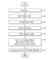
도 1은 본 발명의 실시예에 따른 반도체 장치(100)의 블록도,
도 2는 도 1에 따른 반도체 장치(100)의 리페어 방법을 설명하기 위한 순서도,
도 3은 본 발명의 다른 실시예에 따른 반도체 장치(101)의 블록도이고,
도 4는 도 3에 따른 반도체 장치(101)의 리페어 방법을 설명하기 위한 순서도이다.1 is a block diagram of a
FIG. 2 is a flow chart for explaining a repair method of the
3 is a block diagram of a
FIG. 4 is a flowchart for explaining a repair method of the
이하에서는 첨부된 도면을 참조하여 본 발명의 실시예를 보다 상세히 설명하기로 한다.Hereinafter, embodiments of the present invention will be described in detail with reference to the accompanying drawings.
도 1에 도시된 바와 같이, 본 발명의 실시예에 따른 반도체 장치(100)는 메모리 영역(200), 퓨즈 어레이(300), 잔여 퓨즈정보 저장부(400) 및 제어부(500)를 포함할 수 있다.
1, a
메모리 영역(200)은 메모리 셀 어레이, 복수의 워드 라인(Word Line), 복수의 리던던트 워드 라인(Redundant Word Line) 및 복수의 래치(Latch)를 포함할 수 있다.The
메모리 셀 어레이는 복수의 단위 메모리 블록 예를 들어, 뱅크(Bank)로 구분될 수 있다.The memory cell array may be divided into a plurality of unit memory blocks, for example, a bank.
뱅크는 다시 소 단위의 단위 메모리 블록 예를 들어, 매트(Mat) 등으로 구분될 수 있다.The bank may again be divided into small unit memory blocks, for example, Mat.
복수의 워드 라인은 행(Row) 방향 메모리 셀들의 억세스(Access)가 가능하도록 메모리 셀 어레이와 연결될 수 있다.A plurality of word lines may be coupled to the memory cell array to allow access of memory cells in the row direction.
복수의 워드 라인은 복수의 워드 라인 그룹(WL GRP_0 ~ WL GRP_N)으로 구분될 수 있다.The plurality of word lines may be divided into a plurality of word line groups WLGRP_0 to WLGRP_N.
복수의 워드 라인 그룹(WL GRP_0 ~ WL GRP_N)은 전체 워드 라인들은 예를 들어, 상술한 소 단위의 단위 메모리 블록인 매트(Mat) 단위로 구분한 것일 수 있다.The plurality of word line groups (WLGRP_0 to WLGRP_N) may be formed by dividing all the word lines into, for example, a unit of the above-described unit memory block (Mat).
복수의 리던던트 워드 라인은 페일 어드레스(Fail address)에 대응되는 즉, 복수의 워드 라인 중에서 페일(Fail) 판정된 메모리 셀과 연결된 워드 라인을 대체할 수 있도록 구성될 수 있다.The plurality of redundant word lines may be configured to replace the word lines corresponding to the fail address, that is, the word lines connected to the memory cells determined to fail from the plurality of word lines.
복수의 리던던트 워드 라인은 복수의 리던던트 워드 라인 그룹(RWL GRP_0 ~ RWL GRP_N)으로 구분될 수 있다.The plurality of redundant word lines may be divided into a plurality of redundant word line groups (RWL GRP_0 to RWL GRP_N).
복수의 리던던트 워드 라인 그룹(RWL GRP_0 ~ RWL GRP_N)이 복수의 워드 라인 그룹(WL GRP_0 ~ WL GRP_N)에 1대1 대응되도록 할당될 수 있다.A plurality of redundant word line groups RWL GRP_0 to RWL GRP_N may be assigned to correspond to one word line group WLGRP_0 to WLGRP_N one by one.
복수의 래치(Latch)는 복수의 래치 그룹(LATCH GRP_0 ~ LATCH GRP_N)으로 구분될 수 있다.The plurality of latches can be divided into a plurality of latch groups (LATCH GRP_0 to LATCH GRP_N).
복수의 래치 그룹(LATCH GRP_0 ~ LATCH GRP_N)이 복수의 리던던트 워드 라인 그룹(RWL GRP_0 ~ RWL GRP_N)에 1대1 대응될 수 있다.A plurality of latch groups (LATCH GRP_0 to LATCH GRP_N) can be corresponded one-to-one to a plurality of redundant word line groups (RWL GRP_0 to RWL GRP_N).
복수의 래치 그룹(LATCH GRP_0 ~ LATCH GRP_N) 각각은 복수의 래치 셋(LSETA_0 ~ LSETA_M)을 포함할 수 있다.Each of the plurality of latch groups (LATCH GRP_0 to LATCH GRP_N) may include a plurality of latch sets (LSETA_0 to LSETA_M).
복수의 래치 셋(LSETA_0 ~ LSETA_M)은 각각 페일 어드레스(예를 들어, 13 비트)를 저장할 수 있다.
Each of the plurality of latch sets (LSETA_0 to LSETA_M) may store a fail address (for example, 13 bits).
퓨즈 어레이(300)는 복수의 퓨즈 그룹(FUSE GRP_O ~ FUSE GRP_N)으로 구분될 수 있다.The
복수의 퓨즈 그룹(FUSE GRP_O ~ FUSE GRP_N)은 복수의 래치 그룹(LATCH GRP_0 ~ LATCH GRP_N)에 1대1 대응될 수 있다.A plurality of fuse groups (FUSE GRP_O to FUSE GRP_N) may correspond one-to-one to a plurality of latch groups (LATCH GRP_0 to LATCH GRP_N).
복수의 퓨즈 그룹(FUSE GRP_O ~ FUSE GRP_N)은 각각 복수의 퓨즈 셋(FSET_0 ~ FSET_M)을 포함할 수 있다.The plurality of fuse groups (FUSE GRP_O to FUSE GRP_N) may include a plurality of fuse sets (FSET_0 to FSET_M), respectively.
복수의 퓨즈 셋(FSET_0 ~ FSET_M)은 각각 페일 어드레스(Fail Address)(예를 들어, 13 비트)를 저장할 수 있다.The plurality of fuse sets FSET_0 through FSET_M may each store a fail address (for example, 13 bits).
복수의 퓨즈 셋(FSET_0 ~ FSET_M)은 각각 페일 어드레스의 비트 수에 해당하는 복수의 퓨즈를 포함할 수 있다.The plurality of fuse sets FSET_0 to FSET_M may each include a plurality of fuses corresponding to the number of bits of the fail address.
복수의 퓨즈 셋(FSET_0 ~ FSET_M)은 전자 퓨즈(e-fuse)를 포함할 수 있다.The plurality of fuse sets FSET_0 through FSET_M may include an e-fuse.
럽쳐(Rupture) 동작을 이용하여 복수의 퓨즈 셋(FSET_0 ~ FSET_M)에 페일 어드레스를 저장할 수 있다.The fail address can be stored in the plurality of fuse sets FSET_0 to FSET_M using the Rupture operation.
복수의 퓨즈 셋(FSET_0 ~ FSET_M)은 각 퓨즈 셋의 사용 여부를 정의할 수 있는 인에이블 퓨즈(enable fuse)를 포함할 수 있다.The plurality of fuse sets FSET_0 through FSET_M may include an enable fuse capable of defining whether or not each fuse set is used.
인에이블 퓨즈의 럽쳐 여부에 따라 해당 퓨즈 셋이 사용되었는지 아니면 사용되지 않았는지를 판단할 수 있다.
It can be determined whether the fuse set is used or not, depending on whether the enable fuse is ruptured or not.
잔여 퓨즈정보 저장부(400)는 복수의 퓨즈 그룹(FUSE GRP_O ~ FUSE GRP_N) 각각의 잔여 퓨즈정보를 저장 및 업데이트 시키도록 구성될 수 있다.The residual fuse
이때 잔여 퓨즈정보는 복수의 퓨즈 그룹(FUSE GRP_O ~ FUSE GRP_N) 각각의 복수의 퓨즈 셋(FSET_0 ~ FSET_M) 중에서 사용 가능한 즉, 현재까지 사용되지 않은 퓨즈 셋의 수를 정의할 수 있다.At this time, the residual fuse information may define the number of fusesets that are usable among the plurality of fuse sets FSET_0 to FSET_M of each of the plurality of fuse groups (FUSE GRP_O to FUSE GRP_N), that is, unused fuses.
잔여 퓨즈정보 저장부(400)는 카운터(CNT) 및 복수의 래치 셋(LSETB_0 ~ LSETB_N)을 포함할 수 있다.The residual fuse
복수의 래치 셋(LSETB_0 ~ LSETB_N)은 퓨즈 어레이(300)의 복수의 퓨즈 그룹(FUSE GRP_O ~ FUSE GRP_N)에 1대1 대응될 수 있다.The plurality of latch sets LSETB_0 to LSETB_N may correspond to the plurality of fuse groups FUSE GRP_O to FUSE GRP_N of the
카운터(CNT)는 제어부(500)의 제어에 따라 잔여 퓨즈정보에 맞도록 복수의 래치 셋(LSETB_0 ~ LSETB_N)의 저장 값을 가변시킬 수 있다.
The counter CNT may vary the stored values of the plurality of latch sets LSETB_0 to LSETB_N to match the residual fuse information under the control of the
제어부(500)는 리페어 과정에 필요한 각종 제어 동작을 수행하도록 구성될 수 있다.The
제어부(500)는 반도체 장치를 붓업(Boot-up) 모드로 진입시킬 수 있다.The
제어부(500)는 퓨즈 어레이(300) 스캔을 통해 획득한 잔여 퓨즈정보를 잔여 퓨즈정보 저장부(400)에 저장하고, 테스트 모드에 의해 검출된 페일 어드레스를 잔여 퓨즈정보에 따라 퓨즈 어레이(300)에 저장하기 위한 제어 동작을 수행하도록 구성될 수 있다.The
제어부(500)는 테스트 모드에 의해 검출된 페일 어드레스를 저장하기 위한 래치 셋(LSETC)을 포함할 수 있다.
The
이와 같이 구성된 본 발명의 실시예에 따른 반도체 장치(100)의 리페어 동작을 도 1 및 도 2를 참조하여 설명하기로 한다.The repair operation of the
먼저, 반도체 장치를 붓업 모드로 진입시킨다(S11).First, the semiconductor device enters a push-up mode (S11).
이때 단계(S11)는 제어부(500)에 의해 이루어질 수 있다.At this time, step S11 may be performed by the
제어부(500)는 붓업 모드 구간 동안 퓨즈 어레이(300)를 스캔한다(S12).The
이때 단계(S12)는 퓨즈 어레이(300)의 복수의 퓨즈 그룹(FUSE GRP_O ~ FUSE GRP_N)의 복수의 퓨즈 셋(FSET_0 ~ FSET_M)이 사용되었는지 여부를 판단하는 동작이 될 수 있다.At this time, step S12 may be an operation for determining whether or not a plurality of fuse sets FSET_0 to FSET_M of the plurality of fuse groups FUSE GRP_O to FUSE GRP_N of the
상술한 바와 같이, 복수의 퓨즈 셋(FSET_0 ~ FSET_M)은 각 퓨즈 셋의 사용 여부를 정의할 수 있는 인에이블 퓨즈를 포함할 수 있다.As described above, the plurality of fuse sets FSET_0 through FSET_M may include an enable fuse capable of defining whether or not each fuse set is used.
따라서 단계(S12)는 복수의 퓨즈 그룹(FUSE GRP_O ~ FUSE GRP_N)의 복수의 퓨즈 셋(FSET_0 ~ FSET_M) 각각의 인에이블 퓨즈의 럽쳐 여부를 판단하여 이루어질 수 있다.Accordingly, step S12 may be performed by determining whether or not the enable fuse of each of the plurality of fuse sets FSET_0 to FSET_M of the plurality of fuse groups FUSE GRP_O to FUSE GRP_N is ruptured.
단계(S12)를 수행함에 따라 검출된 잔여 퓨즈정보를 잔여 퓨즈정보 저장부(400)에 저장한다(S13).The residual fuse information detected in step S12 is stored in the residual fuse information storage unit 400 (S13).
이때 단계(S13)는 퓨즈 어레이(300)의 복수의 퓨즈 그룹(FUSE GRP_O ~ FUSE GRP_N) 각각의 잔여 퓨즈정보를 복수의 퓨즈 그룹(FUSE GRP_O ~ FUSE GRP_N)에 1대1 대응되는 잔여 퓨즈정보 저장부(400)의 복수의 래치 셋(LSETB_0 ~ LSETB_N)에 저장하는 단계일 수 있다.At this time, the step S13 stores the residual fuse information of each of the plurality of fuse groups FUSE GRP_O to FUSE GRP_N of the
단계(S13)는 제어부(500)가 잔여 퓨즈정보 저장부(400)를 제어하여 이루어질 수 있다. 제어부(500)의 제어에 따라 잔여 퓨즈정보 저장부(400)의 카운터(CNT)가 복수의 래치 셋(LSETB_0 ~ LSETB_N)의 저장 값을 조정할 수 있다.The step S13 may be performed by the
복수의 퓨즈 그룹(FUSE GRP_O ~ FUSE GRP_N) 각각이 32개의 퓨즈 셋을 포함한다고 가정할 경우, '32'는 5 비트의 2 진수로 나타낼 수 있다.Assuming that each of the plurality of fuse groups (FUSE GRP_O to FUSE GRP_N) includes 32 fuse sets, '32' may be represented by a 5-bit binary number.
'11111'은 잔여 퓨즈 셋이 32개임을 나타낼 수 있고, '11110'은 잔여 퓨즈가 31개임을 나타낼 수 있다. 퓨즈 셋의 사용 개수가 변할 경우, 상술한 방식으로 퓨즈정보 저장부(400)의 카운터(CNT)가 복수의 래치 셋(LSETB_0 ~ LSETB_N)의 저장 값을 조정함으로써 잔여 퓨즈정보 저장이 가능하다.'11111' may indicate that there are 32 remaining fuse sets, and '11110' may indicate that there are 31 remaining fuses. When the number of used fuses is changed, the counter (CNT) of the fuse
따라서 복수의 래치 셋(LSETB_0 ~ LSETB_N) 각각은 잔여 퓨즈정보로서 5비트의 신호를 저장할 수 있다.Therefore, each of the plurality of latch sets LSETB_0 to LSETB_N can store a signal of 5 bits as residual fuse information.
단계(S13) 이후, 반도체 장치(100)를 테스트 모드로 진입시킨다(S14).After the step S13, the
테스트 모드에서 메모리 영역(200)의 메모리 셀 어레이에 대한 테스트를 수행하며, 불량 판정된 메모리 셀에 해당하는 어드레스 즉, 페일 어드레스를 검출한다(S15).In the test mode, the memory cell array of the
단계(S15)에 이어서, 잔여 퓨즈 정보에 대응되는 퓨즈 어레이(300)의 퓨즈 셋을 페일 어드레스에 맞도록 럽쳐한다(S16).Following step S15, the fuse set of the
이때 단계(S16)에서 제어부(500)는 복수의 퓨즈 그룹(FUSE GRP_O ~ FUSE GRP_N) 중에서 페일 어드레스에 대응되는 퓨즈 그룹 예를 들어, FUSE GRP_O을 선택할 수 있다.At this time, in step S16, the
또한 제어부(500)는 잔여 퓨즈정보에 따라 FUSE GRP_O의 복수의 퓨즈 셋(FSET_0 ~ FSET_M) 중에서 사용되지 않은 퓨즈 셋이 럽쳐되도록 퓨즈 어레이(300)를 제어할 수 있다.In addition, the
이때 페일 어드레스가 검출될 때 마다 복수의 퓨즈 셋(FSET_0 ~ FSET_M)을 FSET_0, FSET_1, … FSET_M과 같이 순차적으로 럽쳐하도록 정해져 있을 수 있다.At this time, each time a fail address is detected, a plurality of fuse sets FSET_0 to FSET_M are set as FSET_0, FSET_1, ... FSET_M, and so on.
예를 들어, 복수의 퓨즈 셋(FSET_0 ~ FSET_M) 중에서 FSET_0이 럽쳐된 상태라면, 잔여 퓨즈정보는 FSET_0이 사용되었음을 정의하는 값을 가질 수 있다.For example, if FSET_0 is staggered among the plurality of fuse sets FSET_0 to FSET_M, the residual fuse information may have a value that defines that FSET_0 is used.
따라서 제어부(500)는 잔여 퓨즈정보에 따라 FUSE GRP_O의 복수의 퓨즈 셋(FSET_0 ~ FSET_M) 중에서 사용되지 않은 퓨즈 셋 FSET_1이 럽쳐되도록 퓨즈 어레이(300)를 제어할 수 있다.Therefore, the
단계(S16) 이후, 제어부(500)는 반도체 장치를 리-붓업(Re-Boot-up)시키고, 퓨즈 어레이(300) 스캔을 통해 잔여 퓨즈정보를 업데이트시킨다(S17).After step S16, the
리-붓업 상태에서 제어부(500)는 퓨즈 데이터(FDATA) 즉, 퓨즈 어레이(300)에 저장된 페일 어드레스들을 읽어들여 메모리 영역(200)의 복수의 래치 그룹(LATCH GRP_0 ~ LATCH GRP_N)에 저장할 수 있다.
The
이하, 본 발명의 다른 실시예에 따른 반도체 장치(101) 및 그 리페어 방법을 설명하기로 한다.Hereinafter, a
본 발명의 다른 실시예는 잔여 퓨즈정보 저장부(401)를 하나의 래치 셋(LSETD) 만을 갖도록 구성한다. 그리고 퓨즈 어레이(300) 스캔을 통해 복수의 퓨즈 그룹(FUSE GRP_O ~ FUSE GRP_N) 모두의 잔여 퓨즈정보를 저장하는 동작을 수행하지 않고, 페일 어드레스가 검출될 때 마다 페일 어드레스에 대응되는 복수의 퓨즈 그룹(FUSE GRP_O ~ FUSE GRP_N) 중에서 어느 하나에 대해서만 잔여 퓨즈정보 업데이트 및 해당 퓨즈 셋 럽쳐 동작을 수행하도록 한 것이다.
Another embodiment of the present invention configures the residual fuse
본 발명의 다른 실시예에 따른 반도체 장치(101)는 메모리 영역(200), 퓨즈 어레이(300), 잔여 퓨즈정보 저장부(401) 및 제어부(501)를 포함할 수 있다.
The
메모리 영역(200)은 메모리 셀 어레이, 복수의 워드 라인(Word Line), 복수의 리던던트 워드 라인(Redundant Word Line) 및 복수의 래치(Latch)를 포함할 수 있다.The
메모리 셀 어레이는 복수의 단위 메모리 블록 예를 들어, 뱅크(Bank)로 구분될 수 있다.The memory cell array may be divided into a plurality of unit memory blocks, for example, a bank.
뱅크는 다시 소 단위의 단위 메모리 블록 예를 들어, 매트(Mat) 등으로 구분될 수 있다.The bank may again be divided into small unit memory blocks, for example, Mat.
복수의 워드 라인은 행(Row) 방향 메모리 셀들의 억세스(Access)가 가능하도록 메모리 셀 어레이와 연결될 수 있다.A plurality of word lines may be coupled to the memory cell array to allow access of memory cells in the row direction.
복수의 워드 라인은 복수의 워드 라인 그룹(WL GRP_0 ~ WL GRP_N)으로 구분될 수 있다.The plurality of word lines may be divided into a plurality of word line groups WLGRP_0 to WLGRP_N.
복수의 워드 라인 그룹(WL GRP_0 ~ WL GRP_N)은 전체 워드 라인들은 예를 들어, 상술한 소 단위의 단위 메모리 블록인 매트(Mat) 단위로 구분한 것일 수 있다.The plurality of word line groups (WLGRP_0 to WLGRP_N) may be formed by dividing all the word lines into, for example, a unit of the above-described unit memory block (Mat).
복수의 리던던트 워드 라인은 복수의 워드 라인 중에서 페일(Fail) 판정된 메모리 셀과 연결된 워드 라인을 대체할 수 있도록 구성될 수 있다.The plurality of redundant word lines may be configured to replace the word lines connected to the memory cells determined to fail among the plurality of word lines.
복수의 리던던트 워드 라인은 복수의 리던던트 워드 라인 그룹(RWL GRP_0 ~ RWL GRP_N)으로 구분될 수 있다.The plurality of redundant word lines may be divided into a plurality of redundant word line groups (RWL GRP_0 to RWL GRP_N).
복수의 리던던트 워드 라인 그룹(RWL GRP_0 ~ RWL GRP_N)이 복수의 워드 라인 그룹(WL GRP_0 ~ WL GRP_N)에 1대1 대응되도록 할당될 수 있다.A plurality of redundant word line groups RWL GRP_0 to RWL GRP_N may be assigned to correspond to one word line group WLGRP_0 to WLGRP_N one by one.
복수의 래치(Latch)는 복수의 래치 그룹(LATCH GRP_0 ~ LATCH GRP_N)으로 구분될 수 있다.The plurality of latches can be divided into a plurality of latch groups (LATCH GRP_0 to LATCH GRP_N).
복수의 래치 그룹(LATCH GRP_0 ~ LATCH GRP_N)이 복수의 리던던트 워드 라인 그룹(RWL GRP_0 ~ RWL GRP_N)에 1대1 대응될 수 있다.A plurality of latch groups (LATCH GRP_0 to LATCH GRP_N) can be corresponded one-to-one to a plurality of redundant word line groups (RWL GRP_0 to RWL GRP_N).
복수의 래치 그룹(LATCH GRP_0 ~ LATCH GRP_N) 각각은 복수의 래치 셋(LSETA_0 ~ LSETA_M)을 포함할 수 있다.Each of the plurality of latch groups (LATCH GRP_0 to LATCH GRP_N) may include a plurality of latch sets (LSETA_0 to LSETA_M).
복수의 래치 셋(LSETA_0 ~ LSETA_M)은 각각 페일 어드레스(Fail Address)(예를 들어, 13 비트)를 저장할 수 있다.
Each of the plurality of latch sets LSETA_0 to LSETA_M may store a fail address (for example, 13 bits).
퓨즈 어레이(300)는 복수의 퓨즈 그룹(FUSE GRP_O ~ FUSE GRP_N)으로 구분될 수 있다.The
복수의 퓨즈 그룹(FUSE GRP_O ~ FUSE GRP_N)은 복수의 래치 그룹(LATCH GRP_0 ~ LATCH GRP_N)에 1대1 대응될 수 있다.A plurality of fuse groups (FUSE GRP_O to FUSE GRP_N) may correspond one-to-one to a plurality of latch groups (LATCH GRP_0 to LATCH GRP_N).
복수의 퓨즈 그룹(FUSE GRP_O ~ FUSE GRP_N)은 각각 복수의 퓨즈 셋(FSET_0 ~ FSET_M)을 포함할 수 있다.The plurality of fuse groups (FUSE GRP_O to FUSE GRP_N) may include a plurality of fuse sets (FSET_0 to FSET_M), respectively.
복수의 퓨즈 셋(FSET_0 ~ FSET_M)은 각각 페일 어드레스(Fail Address)(예를 들어, 13 비트)를 저장할 수 있다.The plurality of fuse sets FSET_0 through FSET_M may each store a fail address (for example, 13 bits).
복수의 퓨즈 셋(FSET_0 ~ FSET_M)은 각각 페일 어드레스의 비트 수에 해당하는 복수의 퓨즈를 포함할 수 있다.The plurality of fuse sets FSET_0 to FSET_M may each include a plurality of fuses corresponding to the number of bits of the fail address.
복수의 퓨즈 셋(FSET_0 ~ FSET_M)은 전자 퓨즈(e-fuse)를 포함할 수 있다.The plurality of fuse sets FSET_0 through FSET_M may include an e-fuse.
럽쳐(Rupture) 동작을 이용하여 복수의 퓨즈 셋(FSET_0 ~ FSET_M)에 페일 어드레스를 저장할 수 있다.The fail address can be stored in the plurality of fuse sets FSET_0 to FSET_M using the Rupture operation.
복수의 퓨즈 셋(FSET_0 ~ FSET_M)은 각 퓨즈 셋의 사용 여부를 정의할 수 있는 인에이블 퓨즈(enable fuse)를 포함할 수 있다.The plurality of fuse sets FSET_0 through FSET_M may include an enable fuse capable of defining whether or not each fuse set is used.
인에이블 퓨즈의 럽쳐 여부에 따라 해당 퓨즈 셋이 사용되었는지 아니면 사용되지 않았는지를 판단할 수 있다.
It can be determined whether the fuse set is used or not, depending on whether the enable fuse is ruptured or not.
잔여 퓨즈정보 저장부(401)는 복수의 퓨즈 그룹(FUSE GRP_O ~ FUSE GRP_N) 중에서 현재 검출된 페일 어드레스에 대응되는 어느 하나의 퓨즈 그룹의 잔여 퓨즈정보를 저장 및 업데이트 시키도록 구성될 수 있다.The residual fuse
이때 잔여 퓨즈정보는 복수의 퓨즈 그룹(FUSE GRP_O ~ FUSE GRP_N) 중에서 어느 하나의 복수의 퓨즈 셋(FSET_0 ~ FSET_M) 중에서 사용 가능한 즉, 현재까지 사용되지 않은 퓨즈 셋의 수를 정의할 수 있다.At this time, the remaining fuse information may define the number of fuse sets that can be used among any one of a plurality of fuse sets FSET_0 to FSET_M among the plurality of fuse groups (FUSE GRP_O to FUSE GRP_N), that is, unused fusesets.
잔여 퓨즈정보 저장부(401)는 카운터(CNT) 및 래치 셋(LSETD)을 포함할 수 있다.The residual fuse
래치 셋(LSETD)은 퓨즈 어레이(300)의 복수의 퓨즈 그룹(FUSE GRP_O ~ FUSE GRP_N) 모두에 각각 대응될 수 있다.The latch set LSETD may correspond to all of a plurality of fuse groups (FUSE GRP_O to FUSE GRP_N) of the
카운터(CNT)는 제어부(501)의 제어에 따라 잔여 퓨즈정보에 맞도록 래치 셋(LSETD)의 저장 값을 가변시킬 수 있다.
The counter CNT may vary the stored value of the latch set LSETD according to the residual fuse information under the control of the
제어부(501)는 리페어 과정에 필요한 각종 제어 동작을 수행하도록 구성될 수 있다.The
제어부(501)는 반도체 장치를 붓업(Boot-up) 모드로 진입시킬 수 있다.The
제어부(501)는 페일 어드레스가 검출될 때 마다 퓨즈 어레이(300)의 복수의 퓨즈 그룹(FUSE GRP_O ~ FUSE GRP_N) 중에서 페일 어드레스에 대응되는 어느 하나에 대해서 잔여 퓨즈정보를 업데이트하고 페일 어드레스를 저장하기 위한 제어 동작을 수행하도록 구성될 수 있다.The
제어부(501)는 테스트 모드에 의해 검출된 페일 어드레스를 저장하기 위한 래치 셋(LSETE)을 포함할 수 있다.
The
이와 같이 구성된 본 발명의 다른 실시예에 따른 반도체 장치(101)의 리페어 동작을 도 3 및 도 4를 참조하여 설명하기로 한다.The repair operation of the
먼저, 반도체 장치를 붓업 모드로 진입시킨다(S31).First, the semiconductor device enters a push-up mode (S31).
이때 단계(S31)는 제어부(501)에 의해 이루어질 수 있다.At this time, step S31 may be performed by the
단계(S31)의 붓업 모드 이후, 반도체 장치(101)를 제 1 테스트 모드로 진입시킨다(S32).After the push-up mode of step S31, the
제 1 테스트 모드에서 메모리 영역(200)의 메모리 셀 어레이에 대한 테스트를 수행하며, 불량 판정된 메모리 셀에 해당하는 어드레스 즉, 페일 어드레스를 검출한다(S33).In the first test mode, the memory cell array of the
단계(S33) 이후, 반도체 장치를 리-붓업 시킨다(S34).After step S33, the semiconductor device is re-started up (S34).
제어부(501)는 붓업 모드 구간 동안 퓨즈 어레이(300)의 복수의 퓨즈 그룹(FUSE GRP_O ~ FUSE GRP_N) 중에서 페일 어드레스에 해당하는 퓨즈 그룹을 스캔한다(S35).The
상술한 바와 같이, 복수의 퓨즈 셋(FSET_0 ~ FSET_M)은 각 퓨즈 셋의 사용 여부를 정의할 수 있는 인에이블 퓨즈를 포함할 수 있다.As described above, the plurality of fuse sets FSET_0 through FSET_M may include an enable fuse capable of defining whether or not each fuse set is used.
따라서 단계(S35)는 복수의 퓨즈 그룹(FUSE GRP_O ~ FUSE GRP_N) 중에서 페일 어드레스에 해당하는 어느 하나의 퓨즈 그룹의 복수의 퓨즈 셋(FSET_0 ~ FSET_M) 각각의 인에이블 퓨즈의 럽쳐 여부를 판단하여 이루어질 수 있다.Accordingly, step S35 is performed by determining whether or not the enable fuses of the plurality of fuse sets FSET_0 to FSET_M of one of the plurality of fuse groups FUSE GRP_O to FUSE GRP_N corresponding to the fail address are routed .
단계(S35)를 수행함에 따라 검출된 잔여 퓨즈정보를 잔여 퓨즈정보 저장부(401)에 저장한다(S36).The residual fuse information detected in step S35 is stored in the residual fuse information storage unit 401 (S36).
단계(S36)는 제어부(501)가 잔여 퓨즈정보 저장부(401)를 제어하여 이루어질 수 있다. 제어부(501)의 제어에 따라 잔여 퓨즈정보 저장부(401)의 카운터(CNT)가 래치 셋(LSETE)의 저장 값을 조정할 수 있다.The step S36 may be performed by the
단계(S36) 이후, 반도체 장치(101)를 제 2 테스트 모드로 진입시킨다(S37).After the step S36, the
제 2 테스트 모드에서 잔여 퓨즈 정보에 대응되는 퓨즈 어레이(300)의 퓨즈 셋을 페일 어드레스에 맞도록 럽쳐한다(S38).In the second test mode, the fuse set of the
이때 단계(S38)에서 제어부(501)는 복수의 퓨즈 그룹(FUSE GRP_O ~ FUSE GRP_N) 중에서 페일 어드레스에 대응되는 퓨즈 그룹 예를 들어, FUSE GRP_O을 선택할 수 있다.At this time, in step S38, the
또한 제어부(501)는 잔여 퓨즈정보에 따라 FUSE GRP_O의 복수의 퓨즈 셋(FSET_0 ~ FSET_M) 중에서 사용되지 않은 퓨즈 셋이 럽쳐되도록 퓨즈 어레이(300)를 제어할 수 있다.In addition, the
이때 페일 어드레스가 검출될 때 마다 복수의 퓨즈 셋(FSET_0 ~ FSET_M)을 FSET_0, FSET_1, … FSET_M과 같이 순차적으로 럽쳐하도록 정해져 있을 수 있다.At this time, each time a fail address is detected, a plurality of fuse sets FSET_0 to FSET_M are set as FSET_0, FSET_1, ... FSET_M, and so on.
예를 들어, 복수의 퓨즈 셋(FSET_0 ~ FSET_M) 중에서 FSET_0이 럽쳐된 상태라면, 잔여 퓨즈정보는 FSET_0이 사용되었음을 정의하는 값을 가질 수 있다.For example, if FSET_0 is staggered among the plurality of fuse sets FSET_0 to FSET_M, the residual fuse information may have a value that defines that FSET_0 is used.
따라서 제어부(501)는 잔여 퓨즈정보에 따라 FUSE GRP_O의 복수의 퓨즈 셋(FSET_0 ~ FSET_M) 중에서 사용되지 않은 퓨즈 셋 FSET_1이 럽쳐되도록 퓨즈 어레이(300)를 제어할 수 있다.Accordingly, the
단계(S38) 이후, 제어부(501)는 반도체 장치를 리-붓업 시키고, 퓨즈 어레이(300) 스캔을 통해 잔여 퓨즈정보를 업데이트시킨다(S39).After step S38, the
리-붓업 상태에서 제어부(501)는 퓨즈 데이터(FDATA) 즉, 퓨즈 어레이(300)에 저장된 페일 어드레스들을 읽어들여 메모리 영역(200)의 복수의 래치 그룹(LATCH GRP_0 ~ LATCH GRP_N)에 저장할 수 있다.
The
이와 같이, 본 발명이 속하는 기술분야의 당업자는 본 발명이 그 기술적 사상이나 필수적 특징을 변경하지 않고서 다른 구체적인 형태로 실시될 수 있다는 것을 이해할 수 있을 것이다. 그러므로 이상에서 기술한 실시예들은 모든 면에서 예시적인 것이며 한정적인 것이 아닌 것으로서 이해해야만 한다. 본 발명의 범위는 상기 상세한 설명보다는 후술하는 특허청구범위에 의하여 나타내어지며, 특허청구범위의 의미 및 범위 그리고 그 등가개념으로부터 도출되는 모든 변경 또는 변형된 형태가 본 발명의 범위에 포함되는 것으로 해석되어야 한다.Thus, those skilled in the art will appreciate that the present invention may be embodied in other specific forms without departing from the spirit or essential characteristics thereof. It is therefore to be understood that the embodiments described above are to be considered in all respects only as illustrative and not restrictive. The scope of the present invention is defined by the appended claims rather than the detailed description and all changes or modifications derived from the meaning and scope of the claims and their equivalents are to be construed as being included within the scope of the present invention do.
Claims (12)
복수의 퓨즈 그룹을 포함하며, 상기 메모리 영역의 페일 어드레스를 저장하도록 구성된 퓨즈 어레이;
상기 복수의 퓨즈 그룹 중에서 상기 페일 어드레스에 대응되는 어느 하나의 잔여 퓨즈정보를 저장하도록 구성된 잔여 퓨즈정보 저장부; 및
상기 페일 어드레스가 검출되면 상기 복수의 퓨즈 그룹 중에서 상기 페일 어드레스에 대응되는 어느 하나에 대해서 상기 잔여 퓨즈정보의 업데이트 및 상기 페일 어드레스의 저장을 위한 제어 동작을 수행하도록 구성되는 제어부를 포함하는 반도체 장치.Memory area;
A fuse array including a plurality of groups of fuses, the fuse array configured to store a fail address of the memory region;
A residual fuse information storage configured to store any residual fuse information corresponding to the fail address among the plurality of fuse groups; And
And a control unit configured to perform a control operation for updating the residual fuse information and for storing the fail address in any one of the plurality of fuse groups corresponding to the fail address when the fail address is detected.
상기 메모리 영역은
메모리 셀 어레이,
상기 메모리 셀 어레이와 연결된 복수의 워드 라인 그룹,
상기 복수의 워드 라인 그룹을 대체하기 위한 복수의 리던던트 워드 라인 그룹, 및
상기 복수의 퓨즈 그룹에 대응되는 복수의 래치 그룹을 포함하는 반도체 장치.The method according to claim 1,
The memory region
Memory cell array,
A plurality of word line groups coupled to the memory cell array,
A plurality of redundant word line groups for replacing the plurality of word line groups, and
And a plurality of latch groups corresponding to the plurality of fuse groups.
상기 잔여 퓨즈정보는
상기 복수의 퓨즈 그룹 중에서 어느 하나의 퓨즈 그룹에 포함된 복수의 퓨즈 셋 중에서 사용 가능한 퓨즈 셋의 수를 정의하는 반도체 장치.The method according to claim 1,
The residual fuse information
And defines the number of usable fuses among a plurality of fuses included in one of the plurality of fuse groups.
상기 잔여 퓨즈정보 저장부는
상기 잔여 퓨즈정보를 저장하도록 구성된 래치 셋, 및
상기 잔여 퓨즈정보에 맞도록 상기 래치 셋의 저장 값을 가변시키도록 구성된 카운터를 포함하는 반도체 장치.The method according to claim 1,
The residual fuse information storage unit
A latch set configured to store the residual fuse information, and
And a counter configured to vary the stored value of the latch set to match the residual fuse information.
상기 제어부는
상기 페일 어드레스를 저장하기 위한 래치 셋을 포함하는 반도체 장치.The method according to claim 1,
The control unit
And a latch set for storing the fail address.
제 1 테스트 모드에서 페일 어드레스가 검출되면 반도체 장치를 붓업 시키는 단계;
상기 복수의 퓨즈 그룹 중에서 상기 페일 어드레스에 대응되는 어느 하나의 퓨즈 그룹을 스캔하여 해당 잔여 퓨즈정보를 저장하는 단계; 및
제 2 테스트 모드에서 상기 어느 하나의 퓨즈 그룹의 복수의 퓨즈 셋 중에서 상기 잔여 퓨즈정보에 대응되는 퓨즈 셋에 상기 페일 어드레스를 저장하는 단계를 포함하는 반도체 장치의 리페어 방법.A repair method of a semiconductor device including a fuse array and a memory region divided into a plurality of fuse groups,
When the fail address is detected in the first test mode, the semiconductor device is shut down;
Scanning any of the plurality of fuse groups corresponding to the fail address and storing the residual fuse information; And
And storing the fail address in a fuse set corresponding to the residual fuse information among a plurality of fuse sets of the one of the fuse groups in a second test mode.
상기 제 1 테스트 모드에서 상기 메모리 영역에 대한 테스트를 수행하고, 그에 따라 불량이 발생한 메모리 셀의 어드레스를 상기 페일 어드레스로 검출하는 단계를 더 포함하는 반도체 장치의 리페어 방법.The method according to claim 6,
Performing a test on the memory area in the first test mode and detecting an address of a memory cell in which a failure has occurred as the fail address.
상기 페일 어드레스를 저장하는 단계 이후에,
상기 반도체 장치를 리-붓업 시키고, 상기 어느 하나의 퓨즈 그룹을 스캔하여 해당 잔여 퓨즈정보를 업데이트시키는 단계를 더 포함하는 반도체 장치의 리페어 방법.The method according to claim 6,
After storing the fail address,
Further comprising the step of re-starting the semiconductor device, and scanning any one of the groups of fuses to update the residual fuse information.
상기 페일 어드레스를 저장하는 단계 이후에,
상기 반도체 장치를 리-붓업 시키고, 상기 어느 하나의 퓨즈 그룹을 스캔하여 해당 잔여 퓨즈정보를 업데이트시키는 단계, 및
상기 퓨즈 어레이에 저장된 퓨즈 데이터를 상기 메모리 영역에 저장하는 단계를 더 포함하는 반도체 장치의 리페어 방법.The method according to claim 6,
After storing the fail address,
Re-starting the semiconductor device, scanning any one group of fuses to update the residual fuse information, and
And storing the fuse data stored in the fuse array in the memory area.
상기 반도체 장치를 붓업 시키는 단계;
상기 반도체 장치를 제 1 테스트 모드로 진입시키고 상기 메모리 영역을 테스트하여 페일 어드레스를 검출하는 단계;
상기 페일 어드레스가 검출되면 상기 반도체 장치를 리-붓업 시키는 단계;
상기 복수의 퓨즈 그룹 중에서 상기 페일 어드레스에 대응되는 어느 하나의 퓨즈 그룹을 스캔하여 해당 잔여 퓨즈정보를 저장하는 단계;
상기 반도체 장치를 제 2 테스트 모드로 진입시키고, 상기 어느 하나의 퓨즈 그룹의 복수의 퓨즈 셋 중에서 상기 잔여 퓨즈정보에 대응되는 퓨즈 셋을 상기 페일 어드레스에 맞도록 럽쳐하는 단계를 포함하는 반도체 장치의 리페어 방법.A repair method of a semiconductor device including a fuse array and a memory region divided into a plurality of fuse groups,
A step of pushing up the semiconductor device;
Entering the semiconductor device into a first test mode and testing the memory area to detect a fail address;
Re-entering the semiconductor device when the fail address is detected;
Scanning any of the plurality of fuse groups corresponding to the fail address and storing the residual fuse information;
A step of bringing the semiconductor device into a second test mode and raising the fuse set corresponding to the residual fuse information among the plurality of fuse sets of the one of the fuse groups to match the fail address. Way.
상기 렵쳐하는 단계 이후에,
상기 반도체 장치를 리-붓업 시키고, 상기 어느 하나의 퓨즈 그룹을 스캔하여 해당 잔여 퓨즈정보를 업데이트시키는 단계를 더 포함하는 반도체 장치의 리페어 방법.11. The method of claim 10,
After this awkward step,
Further comprising the step of re-starting the semiconductor device, and scanning any one of the groups of fuses to update the residual fuse information.
상기 렵쳐하는 단계 이후에,
상기 반도체 장치를 리-붓업 시키고, 상기 어느 하나의 퓨즈 그룹을 스캔하여 해당 잔여 퓨즈정보를 업데이트시키는 단계, 및
상기 퓨즈 어레이에 저장된 퓨즈 데이터를 상기 메모리 영역에 저장하는 단계를 더 포함하는 반도체 장치의 리페어 방법.11. The method of claim 10,
After this awkward step,
Re-starting the semiconductor device, scanning any one group of fuses to update the residual fuse information, and
And storing the fuse data stored in the fuse array in the memory area.
Priority Applications (4)
| Application Number | Priority Date | Filing Date | Title |
|---|---|---|---|
| KR1020150099871A KR20170008553A (en) | 2015-07-14 | 2015-07-14 | Semiconductor apparatus and repair method of the same |
| US14/918,816 US9589675B2 (en) | 2015-07-14 | 2015-10-21 | Semiconductor apparatus and repair method thereof |
| CN201510830668.3A CN106356099B (en) | 2015-07-14 | 2015-11-25 | Semiconductor device and method for repairing the same |
| US15/412,268 US9978463B2 (en) | 2015-07-14 | 2017-01-23 | Semiconductor apparatus and repair method thereof |
Applications Claiming Priority (1)
| Application Number | Priority Date | Filing Date | Title |
|---|---|---|---|
| KR1020150099871A KR20170008553A (en) | 2015-07-14 | 2015-07-14 | Semiconductor apparatus and repair method of the same |
Publications (1)
| Publication Number | Publication Date |
|---|---|
| KR20170008553A true KR20170008553A (en) | 2017-01-24 |
Family
ID=57775192
Family Applications (1)
| Application Number | Title | Priority Date | Filing Date |
|---|---|---|---|
| KR1020150099871A KR20170008553A (en) | 2015-07-14 | 2015-07-14 | Semiconductor apparatus and repair method of the same |
Country Status (3)
| Country | Link |
|---|---|
| US (2) | US9589675B2 (en) |
| KR (1) | KR20170008553A (en) |
| CN (1) | CN106356099B (en) |
Families Citing this family (7)
| Publication number | Priority date | Publication date | Assignee | Title |
|---|---|---|---|---|
| KR20170008553A (en) * | 2015-07-14 | 2017-01-24 | 에스케이하이닉스 주식회사 | Semiconductor apparatus and repair method of the same |
| KR20180124568A (en) * | 2017-05-12 | 2018-11-21 | 에스케이하이닉스 주식회사 | Repair circuit for repair operation, and memory device including the same |
| KR102408843B1 (en) * | 2017-08-09 | 2022-06-15 | 에스케이하이닉스 주식회사 | Semiconductor device |
| KR102556939B1 (en) | 2019-04-15 | 2023-07-20 | 에스케이하이닉스 주식회사 | One-time programmable memory circuit and semiconductor apparatus including the same |
| US11244741B1 (en) | 2020-11-04 | 2022-02-08 | Micron Technology, Inc. | Selectable fuse sets, and related methods, devices, and systems |
| CN114999555A (en) * | 2021-03-01 | 2022-09-02 | 长鑫存储技术有限公司 | Fuse fault repair circuit |
| US11587641B2 (en) | 2021-03-01 | 2023-02-21 | Changxin Memory Technologies, Inc. | Fuse fault repair circuit |
Family Cites Families (20)
| Publication number | Priority date | Publication date | Assignee | Title |
|---|---|---|---|---|
| KR940007241B1 (en) * | 1992-03-09 | 1994-08-10 | 삼성전자 주식회사 | Row redundancy device of semiconductor memory device |
| JPH0935493A (en) * | 1995-07-15 | 1997-02-07 | Toshiba Corp | Semiconductor memory, microcontroller and fabrication of semiconductor memory |
| US5835425A (en) * | 1997-09-04 | 1998-11-10 | Siemens Aktiengesellschaft | Dimension programmable fusebanks and methods for making the same |
| US20040123181A1 (en) * | 2002-12-20 | 2004-06-24 | Moon Nathan I. | Self-repair of memory arrays using preallocated redundancy (PAR) architecture |
| JP2004288286A (en) * | 2003-03-20 | 2004-10-14 | Toshiba Lsi System Support Kk | Redundancy fuse circuit |
| US6940773B2 (en) * | 2003-04-02 | 2005-09-06 | Infineon Technologies Ag | Method and system for manufacturing DRAMs with reduced self-refresh current requirements |
| US7289363B2 (en) * | 2005-05-19 | 2007-10-30 | Micron Technology, Inc. | Memory cell repair using fuse programming method in a flash memory device |
| US7373573B2 (en) * | 2005-06-06 | 2008-05-13 | International Business Machines Corporation | Apparatus and method for using a single bank of eFuses to successively store testing data from multiple stages of testing |
| KR100712596B1 (en) * | 2005-07-25 | 2007-04-30 | 삼성전자주식회사 | Method and apparatus for repair and trimming in flash memory device |
| KR20070101910A (en) * | 2006-04-12 | 2007-10-18 | 주식회사 하이닉스반도체 | Semiconductor memory device |
| US8775880B2 (en) * | 2009-06-11 | 2014-07-08 | STMicroelectronics Intenational N.V. | Shared fuse wrapper architecture for memory repair |
| KR101131557B1 (en) * | 2010-04-30 | 2012-04-04 | 주식회사 하이닉스반도체 | Repairing circuit and method of semiconductor memory apparatus |
| KR101190687B1 (en) * | 2010-11-17 | 2012-10-12 | 에스케이하이닉스 주식회사 | Test mode control circuit of semiconductor apparatus and control method of the same |
| KR20120067504A (en) * | 2010-12-16 | 2012-06-26 | 에스케이하이닉스 주식회사 | Fail address storage circuit and redundancy control circuit including the same |
| KR101944936B1 (en) * | 2012-01-12 | 2019-02-07 | 에스케이하이닉스 주식회사 | Fail address storage circuit, redundancy control circuit, method for storing fail address and method for controlling redundancy |
| KR20150001133A (en) * | 2013-06-26 | 2015-01-06 | 삼성전자주식회사 | Semiconductor memory device and repair method thereof |
| KR102117633B1 (en) * | 2013-09-12 | 2020-06-02 | 에스케이하이닉스 주식회사 | Self repair device |
| KR20150130608A (en) * | 2014-05-13 | 2015-11-24 | 에스케이하이닉스 주식회사 | Memory device |
| KR102160598B1 (en) * | 2014-08-05 | 2020-09-28 | 에스케이하이닉스 주식회사 | Semiconductor memory device and operating method thereof |
| KR20170008553A (en) * | 2015-07-14 | 2017-01-24 | 에스케이하이닉스 주식회사 | Semiconductor apparatus and repair method of the same |
-
2015
- 2015-07-14 KR KR1020150099871A patent/KR20170008553A/en unknown
- 2015-10-21 US US14/918,816 patent/US9589675B2/en active Active
- 2015-11-25 CN CN201510830668.3A patent/CN106356099B/en active Active
-
2017
- 2017-01-23 US US15/412,268 patent/US9978463B2/en active Active
Also Published As
| Publication number | Publication date |
|---|---|
| US9589675B2 (en) | 2017-03-07 |
| CN106356099A (en) | 2017-01-25 |
| US20170133109A1 (en) | 2017-05-11 |
| US9978463B2 (en) | 2018-05-22 |
| CN106356099B (en) | 2021-06-25 |
| US20170018316A1 (en) | 2017-01-19 |
Similar Documents
| Publication | Publication Date | Title |
|---|---|---|
| KR20170008553A (en) | Semiconductor apparatus and repair method of the same | |
| US7839707B2 (en) | Fuses for memory repair | |
| KR102117633B1 (en) | Self repair device | |
| US6940765B2 (en) | Repair apparatus and method for semiconductor memory device to be selectively programmed for wafer-level test or post package test | |
| US5867505A (en) | Method and apparatus for testing an integrated circuit including the step/means for storing an associated test identifier in association with integrated circuit identifier for each test to be performed on the integrated circuit | |
| US9805828B1 (en) | Memory apparatus with post package repair | |
| US10541045B2 (en) | Semiconductor apparatus related to the repairing of a redundancy region | |
| KR101936354B1 (en) | Memory device and method for testing the same | |
| US9870837B1 (en) | Semiconductor memory device for performing a post package repair operation and operating method thereof | |
| JPH0222478B2 (en) | ||
| KR20090073094A (en) | Defective block isolation in a non-volatile memory system | |
| KR101967270B1 (en) | Memory device and method for testing the same | |
| US20080282107A1 (en) | Method and Apparatus for Repairing Memory | |
| US6397349B2 (en) | Built-in self-test and self-repair methods and devices for computer memories comprising a reconfiguration memory device | |
| US9076555B2 (en) | Failure diagnosis circuit | |
| US20170040066A1 (en) | Semiconductor apparatus and repair method thereof | |
| US7174477B2 (en) | ROM redundancy in ROM embedded DRAM | |
| US7403417B2 (en) | Non-volatile semiconductor memory device and method for operating a non-volatile memory device | |
| US10535418B2 (en) | Memory device including repair circuit and operation method thereof | |
| US6317846B1 (en) | System and method for detecting faults in computer memories using a look up table | |
| KR20140124545A (en) | Non-volatile memory and boot up operation method of the same | |
| US7454676B2 (en) | Method for testing semiconductor chips using register sets | |
| JP2007280546A (en) | Semiconductor test equipment and semiconductor device testing method | |
| KR100526876B1 (en) | Method for testing memory cell in semiconductor memory | |
| US20210327527A1 (en) | Test method for memory device |