【0001】
【発明の属する技術分野】
本発明は、不良アドレスがプログラムされるリダンダンシイフューズ回路に関し、特に、半導体メモリやメモリ混載マイコンなどのメモリを有する半導体集積回路に使用される。
【0002】
【従来の技術】
半導体メモリやメモリ混載マイコンなどのメモリを有する半導体集積回路においては、メモリセルの微細化などに起因し、製造時にメモリセルの一部に欠陥が発生し、そのメモリセルが不良となる場合がある。この場合、リダンダンシイフューズ回路を用いて、その不良セルを冗長セルに置き換え、チップを救済するという方法が採用される(例えば、特許文献1〜5参照)。
【0003】
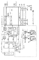
図4は、従来のリダンダンシイフューズ回路を有するメモリ回路の例を示している。
【0004】
メモリセルアレイ10Aは、アレイ状に配置された複数のメモリセルから構成される。メモリセルの種類は、何でも構わない。冗長セルアレイ10Bは、メモリセルアレイ10Aに隣接して配置される。冗長セルアレイ10Bは、アレイ状に配置された複数の冗長セルから構成される。冗長セルは、メモリセルアレイ10A内に不良セルが存在する場合に、その不良セルの代わりとなる。
【0005】
メモリセルアレイ10A内には、複数本、例えば、512本のワード線が配置される。これらワード線は、例えば、8本ごとに、1つのブロックにまとめられ、ブロック単位で、不良セルから冗長セルへの置き換えが実行される。
【0006】
例えば、メモリセルアレイ10Aのテストの結果、メモリセルアレイ10A内の (A) 及び (B) の位置に不良セルが存在していたとすると、不良セルから冗長セルへの置き換えは、これら不良セルを含むブロック内の8つのロウ(8本のワード線)単位で実行される。
【0007】
アドレス信号は、アドレスバッファ11を経由して、アドレスデコーダ12に入力される。アドレスデコーダ12は、アドレス信号をデコードし、メインロウアドレス信号MRA、サブロウアドレス信号SRA及びカラムアドレス信号CAを出力する。
【0008】
メインロウアドレス信号MRAは、メインロウデコーダ13の本体セル分15を経由して、サブロウデコーダ14の本体セル分16に入力される。サブロウアドレス信号SRAは、サブロウデコーダ14内の共通デコーダ17を経由して、サブロウデコーダ14の本体セル分16及びリダンダンシイ(R/D)分19に入力される。カラムアドレス信号CAは、カラムデコーダ20に入力される。
【0009】
例えば、リードデータは、カラム選択スイッチ21、センスアンプ(S/A)22及びバッファ23を経由して、出力データBIT0,BIT1,BITm−1として、チップの外部に出力される。
【0010】
フューズ回路F0,F1,・・・には、それぞれ、不良アドレスがプログラムされる。具体的には、フューズ回路F0,F1,・・・には、不良セルを含むブロックのアドレス(本例では、nビット)がプログラムされる。フューズ回路F0,F1,・・・の数は、例えば、メモリセルアレイ10内の冗長アレイを構成するブロックの数に等しい。
【0011】
フューズ回路F0,F1,・・・は、レーザによるフューズの切断の有無により不良アドレスを記憶するタイプであってもよいし、電気的にフューズを切断できるE(electrically)−フューズを用いていてもよい。フューズ回路F0,F1,・・・は、セレクタSEL0,SEL1,・・・を経由して、オア回路OR1に接続される。
【0012】
メモリセルアレイ10A内に不良セルが存在する場合、セレクタSEL0,SEL1,・・・は、フューズブロック選択信号BLK0,BLK1,・・・に基づいて、1つのフューズ回路Fiを選択する。選択された1つのフューズ回路Fiに対応するセレクタSELiは、そのフューズ回路Fiにプログラムされた不良アドレスを出力する。選択されなかった残りの全てのフューズ回路に対応するセレクタは、そのnビットの出力データを、全て、“0”にする。
【0013】
従って、選択された1つのフューズ回路Fiにプログラムされた不良アドレスは、セレクタSELi及びオア回路OR1を経由して、コンパレータ24に入力される。例えば、フューズブロック選択信号BLK0が“H”、その他のフューズブロック選択信号BLK1,・・・が“L”のとき、フューズ回路F0内にプログラムされたnビットの不良アドレスが、セレクタSEL0及びオア回路OR1を経由して、コンパレータ24に入力される。
【0014】
コンパレータ24は、nビットの外部アドレスデータとオア回路OR1から出力されるnビットの不良アドレスデータとを比較し、両者が一致しない場合には、例えば、フラグFLAGを“L”にする。この時、アドレスデコーダ12が活性化され、通常のデコード動作が実行される。また、コンパレータ24は、両者が一致する場合には、例えば、フラグFLAGを“H”にする。この時、アドレスデコーダ12が非活性化されると共に、メイン/サブロウデコーダ13,14のリダンダンシイ分18,19が活性化される。
【0015】
【特許文献1】
特開2001−307497号公報
【0016】
【特許文献2】
特開平4−322000号公報
【0017】
【特許文献3】
特開平4−238199号公報
【0018】
【特許文献4】
特開平6−243698号公報
【0019】
【特許文献5】
特開平5−128893号公報
【0020】
【発明が解決しようとする課題】
図4に示すような従来のリダンダンシイフューズ回路には、以下の問題がある。
【0021】
▲1▼ テスト工程後、不良セルから冗長セルへの置き換えを行っても、冗長セルに欠陥があるなどの理由により、チップを救済できない場合がある。この場合、フューズを切断する工程が無駄となり、製造コストの増加の原因となる。
【0022】
▲2▼ 不良セルが存在するアドレスとは異なるアドレスを間違ってプログラムしてしまう場合がある。このような場合にも、チップを救済することはできず、フューズを切断する工程が無駄となり、製造コストの増加の原因となる。
【0023】
▲3▼ ▲1▼及び▲2▼に示すように、フューズを切断する工程を経たにもかかわらず、チップを救済できない場合に対し、これを確認するには、フューズを切断した後でなければ行えず、フューズ切断工程が無駄となる。また、フューズは、一度、切断したら、元に戻すことができない。
【0024】
このような問題を、フューズを切断する前に、予め確認できれば、不良を救済できないチップに対しては、フューズ切断工程を行わなくて済むため、製造コストの低減には、効果的である。
【0025】
また、特に、量産前の試作段階においては、フューズ切断工程の環境が十分に整っていないため、フューズ切断時の破片や塵などの影響によるフューズの切断不良が発生する可能性が大きい。そこで、試作段階では、フューズを切断することなく、リダンダンシイフューズ回路の動作確認ができれば、好都合である。
【0026】
本発明の目的は、物理的にフューズを切断しなくても、フューズを切断したと同様の効果を生じさせることができるリダンダンシイフューズ回路を設けることにより、リダンダンシイ置き換えテストの容易化、無駄なフューズ切断工程の排除、及び、間違った不良アドレスのプログラムの防止を図ることにある。
【0027】
【課題を解決するための手段】
本発明の例に関わるリダンダンシイフューズ回路は、メモリセルアレイ内の不良セルを冗長セルに置き換える機能を有し、前記不良セル又はそれを含むブロックのアドレスがフューズの切断の有無により不良アドレスとしてプログラムされるフューズ回路と、テスタから供給される信号をラッチすることにより、前記不良アドレスの擬似的プログラムを行うデータラッチ回路と、前記リダンダンシイフューズ回路の動作確認時に、前記テスタから供給されるアドレス信号と前記データラッチ回路の出力信号とに基づいて、前記不良セルを前記冗長セルに置き換えるコンパレータとを備える。
【0028】
【発明の実施の形態】
以下、図面を参照しながら、本発明の例に関わるリダンダンシイフューズ回路について説明する。
【0029】
1. 概要
本発明の例は、物理的にフューズを切断しなくても、フューズを切断したと同様の効果を生じさせることができるリダンダンシイフューズ回路(リダンダンシイ擬似フューズ回路)に関する。本発明の例に関わるリダンダンシイフューズ回路は、物理的にフューズを切断しなくても、フューズを切断したと同様の効果を発生させることができるため、リダンダンシイ置き換えテストの容易化、無駄なフューズ切断工程の排除や、間違った不良アドレスのプログラムの防止などを図ることができる。
【0030】
本発明の例に関わるリダンダンシイフューズ回路は、メモリを有する半導体集積回路内に設けられ、メモリセルアレイ内の不良セルを冗長セルに置き換える機能を有する。ここで、メモリを有する半導体集積回路には、汎用メモリの他、例えば、メモリ混載マイコンなどが含まれる。
【0031】
さらに、本発明の例は、汎用メモリやメモリ混載マイコンを有する集積回路システムに応用できる。本発明の例は、フューズを実際に切断する前に、それと同様の効果をチップに与えることができるため、リダンダンシイ置き換えによりチップが救済できるか、又は、間違った不良アドレスをプログラムしようとしていないか、などを確認するためのテスト方法に応用できる。
【0032】
2. 第1実施の形態
まず、本発明の第1実施の形態に関わるリダンダンシイフューズ回路について説明する。
【0033】
(1) 全体構成
図1は、本発明の第1実施の形態に関わるリダンダンシイフューズ回路を有するメモリ回路を示している。
【0034】
メモリセルアレイ10Aは、アレイ状に配置された複数のメモリセルから構成される。メモリセルの種類は、RAM、ROMなど、何でも構わない。冗長セルアレイ10Bは、メモリセルアレイ10Aに隣接して配置される。冗長セルアレイ10Bは、アレイ状に配置された複数の冗長セルから構成される。冗長セルは、メモリセルアレイ10A内に不良セルが存在する場合に、その不良セルの代わりとなる。
【0035】
メモリセルアレイ10A内には、複数本、例えば、512本のワード線が配置される。これらワード線は、例えば、8本ごとに、1つのブロックにまとめられ、ブロック単位で、不良セルから冗長セルへの置き換えが実行される。
【0036】
例えば、メモリセルアレイ10Aのテストの結果、メモリセルアレイ10A内の (A) 及び (B) の位置に不良セルが存在していたとすると、不良セルから冗長セルへの置き換えは、これら不良セルを含むブロック内の8つのロウ(8本のワード線)単位で実行される。
【0037】
アドレス信号は、アドレスバッファ11を経由して、アドレスデコーダ12に入力される。アドレスデコーダ12は、アドレス信号をデコードし、メインロウアドレス信号MRA、サブロウアドレス信号SRA及びカラムアドレス信号CAを出力する。
【0038】
メインロウアドレス信号MRAは、メインロウデコーダ13の本体セル分15を経由して、サブロウデコーダ14の本体セル分16に入力される。サブロウアドレス信号SRAは、サブロウデコーダ14内の共通デコーダ17を経由して、サブロウデコーダ14の本体セル分16及びリダンダンシイ(R/D)分19に入力される。カラムアドレス信号CAは、カラムデコーダ20に入力される。
【0039】
例えば、リードデータは、カラム選択スイッチ21、センスアンプ(S/A)22及びバッファ23を経由して、出力データBIT0,BIT1,・・・BITm−1として、チップの外部に出力される。
【0040】
次に、本発明の特徴部分であるリダンダンシイフューズ回路30について説明する。
【0041】
フューズ回路F0,F1,・・・には、それぞれ、不良アドレスがプログラムされる。具体的には、フューズ回路F0,F1,・・・には、不良セルを含むブロックのアドレス(本例では、nビット)がプログラムされる。フューズ回路F0,F1,・・・の数は、例えば、メモリセルアレイ10内の冗長アレイを構成するブロックの数に等しい。
【0042】
フューズ回路F0,F1,・・・は、レーザによるフューズの切断の有無により不良アドレスを記憶するタイプであってもよいし、電気的にフューズを切断できるE(electrically)−フューズを用いていてもよい。フューズ回路F0,F1,・・・は、セレクタSEL0,SEL1,・・・及びアンド回路AND0,AND1,・・・を経由して、オア回路OR1に接続される。
【0043】
本例のリダンダンシイフューズ回路30は、実際にフューズを切断して不良セルを冗長セルに置き換えるセル置き換え機能と、実際にフューズを切断しなくても、フューズを切断したと同様の効果を生じさせる擬似置き換え機能とを有している。これら2つの機能のうちいずれを使用するかは、テスト信号TESTにより決定する。
【0044】
・ セル置き換え機能
通常のセル置き換え機能を使用するときは、テスト信号TESTは、“L”になる。テスト信号TESTが“L”(bTESTが“H”)のときは、データラッチ回路26は、非活性化される。この時、データラッチ回路26の出力データ(nビット)は、全て、“0”になる。
【0045】
一方、アンド回路AND0,AND1,・・・に入力されるテスト信号TESTの反転信号bTESTは、“H”(“1”に相当)である。また、メモリセルアレイ10A内に不良セルが存在する場合、セレクタSEL0,SEL1,・・・は、フューズブロック選択信号BLK0,BLK1,・・・に基づいて、1つのフューズ回路Fiを選択する。選択された1つのフューズ回路Fiに対応するセレクタSELiは、そのフューズ回路Fiにプログラムされた不良アドレスを出力する。選択されなかった残りの全てのフューズ回路に対応するセレクタは、その出力データ(nビット)を、全て、“0”にする。
【0046】
従って、選択された1つのフューズ回路Fiにプログラムされた不良アドレスは、セレクタSELi、アンド回路ANDi及びオア回路OR1を経由して、コンパレータ24に入力される。例えば、フューズブロック選択信号BLK0が“H”、その他のフューズブロック選択信号BLK1,・・・が“L”のとき、フューズ回路F0内にプログラムされたnビットの不良アドレスが、セレクタSEL0、アンド回路AND0及びオア回路OR1を経由して、コンパレータ24に入力される。
【0047】
コンパレータ24は、外部アドレスデータ(nビット)とオア回路OR1から出力される不良アドレスデータ(nビット)とを比較し、両者が一致しない場合には、例えば、フラグFLAGを“L”にする。この時、アドレスデコーダ12が活性化され、通常のデコード動作が実行される。
【0048】
また、コンパレータ24は、両者が一致する場合には、例えば、フラグFLAGを“H”にする。この時、アドレスデコーダ12が非活性化されると共に、メイン/サブロウデコーダ13,14のリダンダンシイ分18,19が活性化される。従って、不良ロウ(8本)内の1つのロウに代わり、冗長ロウ(8本)内の1つのロウが選択される。
【0049】
・ 擬似置き換え機能
実際にフューズを切断しなくても、フューズを切断したと同様の効果を生じさせる擬似置き換え機能を使用するときは、テスト信号TESTは、“H”になる。テスト信号TESTが“H”(bTESTが“L”)のときは、データラッチ回路26は、活性化される。この時、データラッチ回路26は、チップ外部からデータバッファ25を経由して入力される外部アドレス信号(nビット)をラッチする。この外部アドレス信号は、例えば、不良セルを含むブロックのアドレス(不良アドレス)を示している。
【0050】
一方、アンド回路AND0,AND1,・・・に入力されるテスト信号TESTの反転信号bTESTは、“L”(“0”に相当)であるため、全てのアンド回路AND0,AND1,・・・の出力データは、“0”となる。
【0051】
従って、データラッチ回路26にラッチされた外部アドレス信号(不良アドレス)は、オア回路OR1を経由して、コンパレータ24に入力される。このように、例えば、テスト時、物理的にフューズを切断することなく、チップ外部のテスタからリダンダンシイフューズ回路に不良アドレス信号を与えることにより、フューズを切断したときと同様に、不良セルを冗長セルに置き換えることができる。
【0052】
即ち、コンパレータ24は、外部アドレスデータ(nビット)とオア回路OR1から出力される不良アドレスデータ(nビット)とを比較し、両者が一致しない場合には、例えば、フラグFLAGを“L”にする。この時、アドレスデコーダ12が活性化され、通常のデコード動作が実行される。
【0053】
また、コンパレータ24は、両者が一致する場合には、例えば、フラグFLAGを“H”にする。この時、アドレスデコーダ12が非活性化されると共に、メイン/サブロウデコーダ13,14のリダンダンシイ分18,19が活性化される。従って、不良ロウ(8本)内の1つのロウに代わり、冗長ロウ(8本)内の1つのロウが選択される。
【0054】
(2) 動作
次に、本発明の第1実施の形態に関わるリダンダンシイフューズ回路の動作について説明する。
【0055】
本実施の形態では、図1に示すように、不良セルから冗長セルへの置き換えは、8つのロウ(8本のワード線)単位で実行される。メモリセルアレイ10Aのテストの結果、不良セルがA及びBの位置に存在していたとする。
【0056】
まず、不良セルから冗長セルへの置き換えにより、チップが救済できるか否かを検証するテストモードに入る。
【0057】
テスト信号TESTが“H”(bTESTが“L”)になるため、データラッチ回路26が活性化され、アンド回路AND0,AND1,・・・の出力データは、全て、“0”となる。
【0058】
リセット信号RSTによりデータラッチ回路26がリセットされた後、テスタにより生成された外部アドレス信号(不良アドレス)は、データバッファ25を経由し、クロック信号CLKに同期してデータラッチ回路26にラッチされる。
【0059】
コンパレータ24は、外部アドレスデータ(nビット)とオア回路OR1から出力されるラッチデータ(nビット)とを比較し、両者が一致しない場合には、例えば、フラグFLAGを“L”にする。この時、アドレスデコーダ12が活性化され、通常のデコード動作が実行される。
【0060】
また、コンパレータ24は、両者が一致する場合には、例えば、フラグFLAGを“H”にする。この時、アドレスデコーダ12が非活性化されると共に、メイン/サブロウデコーダ13,14のリダンダンシイ分18,19が活性化される。これにより、不良ロウ(8本)が冗長ロウ(8本)に置き換えられる。そして、ロウアドレス信号により、冗長ロウ(8本)のうちから1つのロウが選択される。
【0061】
ここで、リダンダンシイフューズ回路の動作確認を行うテストモードでは、図3に示すように、実際に、データの書き込み及び読み出しを行い、書き込みデータと読み出しデータが一致するか否かを検証する(図3の「不良アドレスの擬似プログラム+テスト」に相当)。
【0062】
両者が一致する場合には、不良セルから冗長セルへの置き換えによりチップが救済できたことを意味しているため、この後、実際に、フューズの切断を実行する。これに対し、両者が一致しない場合には、不良セルから冗長セルへの置き換えによってもチップが救済できなかったことを意味しているため、そのチップは、不良品として処理する。
【0063】
(3) 効果
このように、本発明の第1実施の形態によれば、冗長ロウを有するメモリ回路に関して、物理的にフューズを切断しなくても、フューズを切断したと同様の効果を生じさせることができる。即ち、フューズを切断することなく、リダンダンシイフューズ回路の動作確認を行えるため、リダンダンシイ置き換えテストの容易化、無駄なフューズ切断工程の排除、及び、間違った不良アドレスのプログラムの防止を図ることができる。
【0064】
3. 第2実施の形態
まず、本発明の第2実施の形態に関わるリダンダンシイフューズ回路について説明する。
【0065】
(1) 全体構成
図2は、本発明の第2実施の形態に関わるリダンダンシイフューズ回路を有するメモリ回路を示している。
【0066】
上述の第1実施の形態では、本発明の例に関わるリダンダンシイフューズ回路を、冗長ロウを有するメモリ回路に適用した。これに対し、第2実施の形態では、本発明の例に関わるリダンダンシイフューズ回路を、冗長カラムを有するメモリ回路に適用する。
【0067】
メモリセルアレイ10Aは、アレイ状に配置された複数のメモリセルから構成される。メモリセルの種類は、RAM、ROMなど、何でも構わない。冗長セルアレイ10Bは、メモリセルアレイ10Aに隣接して配置される。冗長セルアレイ10Bは、アレイ状に配置された複数の冗長セルから構成される。冗長セルは、メモリセルアレイ10A内に不良セルが存在する場合に、その不良セルの代わりとなる。
【0068】
メモリセルアレイ10A内には、複数本のビット線が配置される。これらビット線は、例えば、32本ごとに、1つのブロックにまとめられ、ブロック単位で、不良セルから冗長セルへの置き換えが実行される。
【0069】
例えば、メモリセルアレイ10Aのテストの結果、メモリセルアレイ10A内の (A) 及び (B) の位置に不良セルが存在していたとすると、不良セルから冗長セルへの置き換えは、これら不良セルを含むブロック内の32カラム(32本のビット線)単位で実行される。
【0070】
アドレス信号は、アドレスバッファ11を経由して、アドレスデコーダ12に入力される。アドレスデコーダ12は、アドレス信号をデコードし、メインロウアドレス信号MRA、サブロウアドレス信号SRA、カラムアドレス信号CA及びI/O切り替え信号I/O・SELを出力する。
【0071】
メインロウアドレス信号MRA及びサブロウアドレス信号SRAは、メインロウデコーダ13又はサブロウデコーダ14に入力される。メインロウデコーダ13及びサブロウデコーダ14の構成は、第1実施の形態(図1)と同じであるため、ここでは、その説明を省略する。カラムアドレス信号CAは、カラムデコーダ20に入力される。I/O切り替え信号I/O・SELは、カラムデコーダ20及びリダンダンシイ(R/D)カラム制御回路27に入力される。
【0072】
例えば、不良セルから冗長セルへの置き換えを行う場合、不良アドレスに対応するブロックでは、ヒット信号HITCOLが“H”になり、I/O切り替え信号I/O・SELが“H”になる。この時、不良アドレスに対応するブロックでは、カラムデコーダ20が非活性化され、リダンダンシイ(R/D)カラム制御回路27が活性化される。リダンダンシイ(R/D)カラム制御回路27は、冗長セルアレイ10Bからデータが出力されるように、カラムスイッチ21を制御する。なお、カラムデコーダ20を非活性化せずに、I/Oバッファ23において不良カラムを冗長カラムに置き換えるようにしてもよい。
【0073】
不良アドレスに対応するブロック以外のブロックでは、カラムデコーダ20が活性化され、リダンダンシイ(R/D)カラム制御回路27が非活性化される。カラムデコーダ20及びリダンダンシイ(R/D)カラム制御回路27は、32カラム(32本のビット線)のうちの1つを選択し、選択された1つのカラムのカラム選択スイッチをオンにする。なお、リダンダンシイ(R/D)カラム制御回路27を非活性化せずに、I/Oバッファ23において、冗長カラムではなく、通常カラムを選択するようにしてもよい。
【0074】
リードデータは、カラム選択スイッチ21、センスアンプ(S/A)22及びバッファ23を経由して、出力データBIT0,BIT1,・・・BITmとして、チップの外部に出力される。
【0075】
次に、本発明の特徴部分であるリダンダンシイフューズ回路30について説明する。
【0076】
フューズ回路F0,F1,・・・には、それぞれ、不良アドレスがプログラムされる。具体的には、フューズ回路F0,F1,・・・には、不良セルのアドレス(本例では、xビット)がプログラムされる。フューズ回路F0,F1,・・・の数は、例えば、メモリセルアレイ10内の冗長アレイを構成するブロックの数に等しい。
【0077】
フューズ回路F0,F1,・・・は、レーザによるフューズの切断の有無により不良アドレスを記憶するタイプであってもよいし、電気的にフューズを切断できるE(electrically)−フューズを用いていてもよい。フューズ回路F0,F1,・・・は、セレクタSEL0,SEL1,・・・及びアンド回路AND0,AND1,・・・を経由して、オア回路OR1に接続される。
【0078】
本例のリダンダンシイフューズ回路30は、実際にフューズを切断して不良セルを冗長セルに置き換えるセル置き換え機能と、実際にフューズを切断しなくても、フューズを切断したと同様の効果を生じさせる擬似置き換え機能とを有している。これら2つの機能のうちいずれを使用するかは、テスト信号TESTにより決定する。
【0079】
・ セル置き換え機能
通常のセル置き換え機能を使用するときは、テスト信号TESTは、“L”になる。テスト信号TESTが“L”(bTESTが“H”)のときは、データラッチ回路26は、非活性化される。この時、データラッチ回路26の出力データ(xビット)は、全て、“0”になる。
【0080】
一方、アンド回路AND0,AND1,・・・に入力されるテスト信号TESTの反転信号bTESTは、“H”(“1”に相当)である。また、メモリセルアレイ10A内に不良セルが存在する場合、セレクタSEL0,SEL1,・・・は、フューズブロック選択信号BLK0,BLK1,・・・に基づいて、1つのフューズ回路Fiを選択する。選択された1つのフューズ回路Fiに対応するセレクタSELiは、そのフューズ回路Fiにプログラムされた不良アドレスを出力する。選択されなかった残りの全てのフューズ回路に対応するセレクタは、その出力データ(xビット)を、全て、“0”にする。
【0081】
従って、選択された1つのフューズ回路Fiにプログラムされた不良アドレスは、セレクタSELi、アンド回路ANDi及びオア回路OR1を経由して、コンパレータ24に入力される。例えば、フューズブロック選択信号BLK0が“H”、その他のフューズブロック選択信号BLK1,・・・が“L”のとき、フューズ回路F0内にプログラムされたxビットの不良アドレスが、セレクタSEL0、アンド回路AND0及びオア回路OR1を経由して、コンパレータ24に入力される。
【0082】
コンパレータ24は、外部アドレスデータ(xビット)とオア回路OR1から出力される不良アドレスデータ(xビット)とを比較し、両者が一致しない場合には、例えば、ヒット信号HITCOLを“L”にする。
【0083】
この時、アドレスデコーダ12は、I/O切り替え信号I/O・SELを“L”にする。従って、カラムデコーダ20が活性化され、リダンダンシイ(R/D)カラム制御回路27が非活性化され、通常のデコード動作が実行される。
【0084】
また、ヒット信号HITCOLが“L”のとき、セレクタ29の出力信号SW0,SW1,・・・は、全て、“L”になる。従って、バッファ23は、メモリセルアレイ10Aから読み出されたデータを選択し、これを、リードデータBIT0,BIT1,・・・BITm−1として出力する。
【0085】
これに対し、コンパレータ24は、両者が一致する場合には、例えば、ヒット信号HITCOLを“H”にする。
【0086】
この時、アドレスデコーダ12は、I/O切り替え信号I/O・SELを“H”にする。従って、カラムデコーダ20が非活性化され、リダンダンシイ(R/D)カラム制御回路27が活性化される。リダンダンシイ(R/D)カラム制御回路27は、不良アドレス信号(xビット)に対応するブロックiについては、冗長セルアレイ10Bからデータが出力されるように、カラムスイッチ21を制御する。
【0087】
また、ヒット信号HITCOLが“H”のとき、セレクタ29は、I/O切り替えデコーダ28の出力信号を選択する。I/O切り替えデコーダ28は、オア回路OR1から出力される不良アドレス信号(pビット)をデコードし、その不良アドレス信号により特定されるブロックiについてのみ、切り替え信号SWiを“H”にする。
【0088】
例えば、不良アドレス信号(pビット)によりカラム0(ブロック0)が特定される場合には、切り替え信号SW0が“H”となり、その他の切り替え信号SW1,・・・は、全て、“L”になる。従って、カラム0に関しては、バッファ23は、冗長セルアレイ10Bから読み出されたデータを選択し、これを、リードデータBIT0として出力する。また、カラム0以外のカラムに関しては、バッファ23は、メモリセルアレイ10Aから読み出されたデータを選択し、これを、リードデータBIT1,・・・BITm−1として出力する。
【0089】
・ 擬似置き換え機能
実際にフューズを切断しなくても、フューズを切断したと同様の効果を生じさせる擬似置き換え機能を使用するときは、テスト信号TESTは、“H”になる。テスト信号TESTが“H”(bTESTが“L”)のときは、データラッチ回路26は、活性化される。この時、データラッチ回路26は、チップ外部からデータバッファ25を経由して入力される外部アドレス信号(xビット)をラッチする。この外部アドレス信号は、例えば、不良セルのアドレス(不良アドレス)を示している。
【0090】
一方、アンド回路AND0,AND1,・・・に入力されるテスト信号TESTの反転信号bTESTは、“L”(“0”に相当)であるため、全てのアンド回路AND0,AND1,・・・の出力データは、“0”となる。
【0091】
従って、データラッチ回路26にラッチされた外部アドレス信号(不良アドレス)は、オア回路OR1を経由して、コンパレータ24に入力される。このように、例えば、テスト時、物理的にフューズを切断することなく、チップ外部のテスタからリダンダンシイフューズ回路に不良アドレス信号を与えることにより、フューズを切断したときと同様に、不良セルを冗長セルに置き換えることができる。
【0092】
即ち、コンパレータ24は、外部アドレスデータ(xビット)とオア回路OR1から出力される不良アドレスデータ(xビット)とを比較し、両者が一致しない場合には、例えば、ヒット信号HITCOLを“L”にする。
【0093】
この時、アドレスデコーダ12は、I/O切り替え信号I/O・SELを“L”にする。従って、カラムデコーダ20が活性化され、リダンダンシイ(R/D)カラム制御回路27が非活性化され、通常のデコード動作が実行される。
【0094】
また、ヒット信号HITCOLが“L”のとき、セレクタ29の出力信号SW0,SW1,・・・は、全て、“L”になる。従って、バッファ23は、メモリセルアレイ10Aから読み出されたデータを選択し、これを、リードデータBIT0,BIT1,・・・BITm−1として出力する。
【0095】
これに対し、コンパレータ24は、両者が一致する場合には、例えば、ヒット信号HITCOLを“H”にする。
【0096】
この時、アドレスデコーダ12は、I/O切り替え信号I/O・SELを“H”にする。従って、カラムデコーダ20が非活性化され、リダンダンシイ(R/D)カラム制御回路27が活性化される。リダンダンシイ(R/D)カラム制御回路27は、不良アドレス信号(xビット)に対応するブロックiについては、冗長セルアレイ10Bからデータが出力されるように、カラムスイッチ21を制御する。
【0097】
また、ヒット信号HITCOLが“H”のとき、セレクタ29は、I/O切り替えデコーダ28の出力信号を選択する。I/O切り替えデコーダ28は、オア回路OR1から出力される不良アドレス信号(pビット)をデコードし、その不良アドレス信号により特定されるブロックiについてのみ、切り替え信号SWiを“H”にする。
【0098】
例えば、不良アドレス信号(pビット)によりカラム0(ブロック0)が特定される場合には、切り替え信号SW0が“H”となり、その他の切り替え信号SW1,・・・は、全て、“L”になる。従って、カラム0に関しては、バッファ23は、冗長セルアレイ10Bから読み出されたデータを選択し、これを、リードデータBIT0として出力する。また、カラム0以外のカラムに関しては、バッファ23は、メモリセルアレイ10Aから読み出されたデータを選択し、これを、リードデータBIT1,・・・BITm−1として出力する。
【0099】
(2) 動作
次に、本発明の第2実施の形態に関わるリダンダンシイフューズ回路の動作について説明する。
【0100】
本実施の形態では、図2に示すように、不良セルから冗長セルへの置き換えは、ブロック単位、即ち、32カラム(32本のビット線)単位で実行される。メモリセルアレイ10Aのテストの結果、不良セルがA及びBの位置に存在していたとする。
【0101】
まず、不良セルから冗長セルへの置き換えにより、チップが救済できるか否かを検証するテストモードに入る。
【0102】
テスト信号TESTが“H”(bTESTが“L”)になるため、データラッチ回路26が活性化され、アンド回路AND0,AND1,・・・の出力データは、全て、“0”となる。
【0103】
リセット信号RSTによりデータラッチ回路26がリセットされた後、テスタにより生成された外部アドレス信号(不良アドレス)は、データバッファ25を経由し、クロック信号CLKに同期してデータラッチ回路26にラッチされる。
【0104】
コンパレータ24は、外部アドレスデータ(xビット)とオア回路OR1から出力されるラッチデータ(xビット)とを比較し、両者が一致しない場合には、例えば、ヒット信号HITCOLを“L”にする。この時、カラムデコーダ20が活性化され、通常のデコード動作が実行される。
【0105】
また、コンパレータ24は、両者が一致する場合には、例えば、ヒット信号HITCOLを“H”にする。この時、不良アドレス信号に対応するブロックでは、カラムデコーダ20が非活性化されると共に、リダンダンシイ(R/D)カラム制御回路27が活性化される。これにより、不良アドレス信号に対応するブロック内の不良カラム(32本)が冗長カラム(32本)に置き換えられる。そして、カラムアドレス信号により、冗長カラム(32本)のうちから1つのカラムが選択される。
【0106】
ここで、リダンダンシイフューズ回路の動作確認を行うテストモードでは、図3に示すように、実際に、データの書き込み及び読み出しを行い、書き込みデータと読み出しデータが一致するか否かを検証する(図3の「不良アドレスの擬似プログラム+テスト」に相当)。
【0107】
両者が一致する場合には、不良セルから冗長セルへの置き換えによりチップが救済できたことを意味しているため、この後、実際に、フューズの切断を実行する。これに対し、両者が一致しない場合には、不良セルから冗長セルへの置き換えによってもチップが救済できなかったことを意味しているため、そのチップは、不良品として処理する。
【0108】
(3) 効果
このように、本発明の第2実施の形態によれば、冗長カラムを有するメモリ回路に関して、物理的にフューズを切断しなくても、フューズを切断したと同様の効果を生じさせることができる。即ち、フューズを切断することなく、リダンダンシイフューズ回路の動作確認を行えるため、リダンダンシイ置き換えテストの容易化、無駄なフューズ切断工程の排除、及び、間違った不良アドレスのプログラムの防止を図ることができる。
【0109】
4. テスト方法
図3は、リダンダンシイ置き換えテストに関して、本発明と従来とを比較したものである。
【0110】
従来では、メモリセルアレイ本体のテストを行い、不良セルが確認されると、不良アドレスのプログラム(フューズ切断)が実行される(ステップST1〜ST2)。この後、リダンダンシイフューズ回路の動作確認(テスト)を実行し、正常に動作すれば、良品、正常に動作しなければ、不良品として処理する(ステップST3)。この場合、フューズを切断しなければ、最終的に、製品が良品となるか、不良品となるかは、判断できない。
【0111】
これに対し、本発明の例では、メモリセルアレイ本体のテストを行い、不良セルが確認されると、不良アドレスの擬似プログラム及びリダンダンシイフューズ回路の動作確認(テスト)が実行される(ステップST1〜ST2)。そして、リダンダンシイフューズ回路が正常に動作すれば、良品、正常に動作しなければ、不良品として処理する。つまり、正常と判断された製品についてのみ、不良アドレスのプログラム、即ち、フューズの切断を行えばよい(ステップST3)。
【0112】
5. その他
本発明の例は、リダンダンシイフューズ回路に適用されたが、これに限られず、フューズ素子を有する回路に広く適用できる。即ち、本発明の例は、フューズ素子を有する回路に関して、フューズ素子を切断することなく、その動作確認を行う場合に有効である。
【0113】
【発明の効果】
以上、説明したように、本発明の例によれば、リダンダンシイフューズ回路によるセルの置き換えを、実際にフューズを切断することなく、電気的に擬似的に行うことができる。このため、フューズを切断する前のテスト動作により、不良セルが救済可能か否かのチェックを行うことができる。その結果、例えば、量産前の試作段階などのフューズカットの環境が整っていない状況でも、容易に、リダンダンシイ置き換えテストを行え、歩留り向上などを実現できる。
【図面の簡単な説明】
【図1】本発明の第1実施の形態に関わるリダンダンシイフューズ回路を示す回路図。
【図2】本発明の第2実施の形態に関わるリダンダンシイフューズ回路を示す回路図。
【図3】本発明の例に関わる置き換えテストを従来のそれと比較して示す図。
【図4】従来のリダンダンシイフューズ回路を示す回路図。
【符号の説明】
10A: メモリセルアレイ、 10B: 冗長セルアレイ、 11: アドレスバッファ、 12: アドレスデコーダ、 13: メインロウデコーダ、14: サブロウデコーダ、 15: メインロウデコーダの本体セル分、 16: サブロウデコーダの本体セル分、 17: 共通デコーダ、 18: メインロウデコーダのリダンダンシイ分、 19: サブロウデコーダのリダンダンシイ分、 20: カラムデコーダ、 21: カラム選択スイッチ、 22: センスアンプ、 23: バッファ、 24: コンパレータ、 25:データバッファ、 26: データラッチ回路、 27: リダンダンシイカラム制御回路、 28: I/O切り替えデコーダ、 29: セレクタ、 30: リダンダンシイフューズ回路、F0,F1,・・・: フューズ回路、 SEL0,SEL1,・・・: セレクタ、 AND0,AND1,・・・: アンド回路、 OR1: オア回路。[0001]
TECHNICAL FIELD OF THE INVENTION
The present invention relates to a redundancy fuse circuit in which a defective address is programmed, and is particularly used for a semiconductor integrated circuit having a memory such as a semiconductor memory or a memory-mixed microcomputer.
[0002]
[Prior art]
2. Description of the Related Art In a semiconductor integrated circuit having a memory such as a semiconductor memory or a memory-mixed microcomputer, a part of the memory cell may be defective at the time of manufacture due to the miniaturization of the memory cell and the memory cell may be defective. . In this case, a method of using a redundancy fuse circuit to replace the defective cell with a redundant cell and rescue the chip is adopted (for example, see Patent Documents 1 to 5).
[0003]
FIG. 4 shows an example of a memory circuit having a conventional redundancy fuse circuit.
[0004]
The memory cell array 10A includes a plurality of memory cells arranged in an array. Any type of memory cell may be used. The redundant cell array 10B is arranged adjacent to the memory cell array 10A. The redundant cell array 10B includes a plurality of redundant cells arranged in an array. When a defective cell exists in the memory cell array 10A, the redundant cell substitutes for the defective cell.
[0005]
A plurality of, for example, 512 word lines are arranged in the memory cell array 10A. For example, these word lines are grouped into one block every eight lines, and replacement of a defective cell with a redundant cell is performed in block units.
[0006]
For example, as a result of the test of the memory cell array 10A, assuming that defective cells exist at the positions (A) and (B) in the memory cell array 10A, the replacement of the defective cell with the redundant cell is performed by using a block including these defective cells. Is executed in units of eight rows (eight word lines).
[0007]
The address signal is input to the address decoder 12 via the address buffer 11. The address decoder 12 decodes an address signal and outputs a main row address signal MRA, a sub row address signal SRA, and a column address signal CA.
[0008]
The main row address signal MRA is input to the main cell 16 of the sub-row decoder 14 via the main cell 15 of the main row decoder 13. The sub-row address signal SRA is input to the main cell 16 and the redundancy (R / D) 19 of the sub-row decoder 14 via the common decoder 17 in the sub-row decoder 14. The column address signal CA is input to the column decoder 20.
[0009]
For example, the read data is output to the outside of the chip as output data BIT0, BIT1, and BITm-1 via the column selection switch 21, the sense amplifier (S / A) 22, and the buffer 23.
[0010]
Each of the fuse circuits F0, F1,... Is programmed with a defective address. Specifically, an address (n bits in this example) of a block including a defective cell is programmed in the fuse circuits F0, F1,. The number of the fuse circuits F0, F1,... Is, for example, equal to the number of blocks constituting the redundant array in the memory cell array 10.
[0011]
The fuse circuits F0, F1,... May be of a type that stores a defective address depending on whether or not the fuse is cut by a laser, or may be an E (electrically) -fuse that can electrically cut the fuse. Good. The fuse circuits F0, F1,... Are connected to the OR circuit OR1 via the selectors SEL0, SEL1,.
[0012]
When a defective cell exists in the memory cell array 10A, the selectors SEL0, SEL1,... Select one fuse circuit Fi based on the fuse block selection signals BLK0, BLK1,. The selector SELi corresponding to the selected one fuse circuit Fi outputs a defective address programmed in the fuse circuit Fi. The selectors corresponding to all the remaining unselected fuse circuits set all the n-bit output data to “0”.
[0013]
Therefore, the defective address programmed in the selected one fuse circuit Fi is input to the comparator 24 via the selector SELi and the OR circuit OR1. For example, when the fuse block selection signal BLK0 is “H” and the other fuse block selection signals BLK1,... Are “L”, the n-bit defective address programmed in the fuse circuit F0 is determined by the selector SEL0 and the OR circuit. The signal is input to the comparator 24 via OR1.
[0014]
The comparator 24 compares the n-bit external address data with the n-bit defective address data output from the OR circuit OR1, and if they do not match, for example, sets the flag FLAG to “L”. At this time, the address decoder 12 is activated, and a normal decoding operation is performed. If the two match, the comparator 24 sets the flag FLAG to “H”, for example. At this time, the address decoder 12 is deactivated and the redundancy components 18 and 19 of the main / sub row decoders 13 and 14 are activated.
[0015]
[Patent Document 1]
JP 2001-307497 A
[0016]
[Patent Document 2]
JP-A-4-322000
[0017]
[Patent Document 3]
JP-A-4-238199
[0018]
[Patent Document 4]
JP-A-6-243698
[0019]
[Patent Document 5]
JP-A-5-128893
[0020]
[Problems to be solved by the invention]
The conventional redundancy fuse circuit as shown in FIG. 4 has the following problems.
[0021]
{Circle around (1)} Even after replacing a defective cell with a redundant cell after the test process, there is a case where the chip cannot be rescued due to a defect in the redundant cell or the like. In this case, the step of cutting the fuse is wasted and causes an increase in manufacturing cost.
[0022]
{Circle around (2)} An address different from the address where the defective cell exists may be erroneously programmed. Even in such a case, the chip cannot be rescued, and the step of cutting the fuse is wasted, resulting in an increase in manufacturing cost.
[0023]
(3) As shown in (1) and (2), in the case where the chip cannot be rescued even though the fuse has been cut, the only way to confirm this is to make sure that the fuse has been cut. Cannot be performed, and the fuse cutting step is wasted. Also, once a fuse has been cut, it cannot be restored.
[0024]
If such a problem can be confirmed in advance before cutting the fuse, it is not necessary to perform the fuse cutting step for a chip whose defect cannot be remedied, which is effective in reducing the manufacturing cost.
[0025]
In addition, particularly in a prototype stage before mass production, the environment of the fuse cutting process is not sufficiently prepared, so that there is a high possibility that a fuse may fail to be cut due to the influence of debris or dust during the fuse cutting. Therefore, it is convenient if the operation of the redundancy fuse circuit can be confirmed without cutting the fuse at the prototype stage.
[0026]
SUMMARY OF THE INVENTION An object of the present invention is to provide a redundancy fuse circuit capable of producing the same effect as a blown fuse without physically blowing the fuse, thereby facilitating a redundancy replacement test and reducing wastefulness. An object of the present invention is to eliminate a fuse cutting step and prevent programming of an incorrect defective address.
[0027]
[Means for Solving the Problems]
The redundancy fuse circuit according to the example of the present invention has a function of replacing a defective cell in a memory cell array with a redundant cell, and an address of the defective cell or a block including the defective cell is programmed as a defective address depending on whether or not the fuse is cut. A data latch circuit for performing pseudo-programming of the defective address by latching a signal supplied from the tester, and an address signal supplied from the tester when confirming the operation of the redundancy fuse circuit. A comparator that replaces the defective cell with the redundant cell based on the output signal of the data latch circuit.
[0028]
BEST MODE FOR CARRYING OUT THE INVENTION
Hereinafter, a redundancy fuse circuit according to an example of the present invention will be described with reference to the drawings.
[0029]
1. Overview
An example of the present invention relates to a redundancy fuse circuit (redundancy pseudo-fuse circuit) that can produce the same effect as a blown fuse without physically blowing the fuse. The redundancy fuse circuit according to the example of the present invention can produce the same effect as that of cutting the fuse without physically cutting the fuse. It is possible to eliminate the cutting step, prevent the programming of the wrong defective address, and the like.
[0030]
The redundancy fuse circuit according to the example of the present invention is provided in a semiconductor integrated circuit having a memory and has a function of replacing a defective cell in a memory cell array with a redundant cell. Here, a semiconductor integrated circuit having a memory includes, for example, a microcomputer with embedded memory in addition to a general-purpose memory.
[0031]
Further, the example of the present invention can be applied to an integrated circuit system having a general-purpose memory or a microcomputer with a memory. Since the example of the present invention can give the same effect to the chip before the fuse is actually cut, whether the chip can be relieved by redundancy replacement or whether the wrong defective address is being programmed. It can be applied to a test method for confirming, for example.
[0032]
2. First embodiment
First, a redundancy fuse circuit according to the first embodiment of the present invention will be described.
[0033]
(1) Overall configuration
FIG. 1 shows a memory circuit having a redundancy fuse circuit according to the first embodiment of the present invention.
[0034]
The memory cell array 10A includes a plurality of memory cells arranged in an array. Any type of memory cell, such as a RAM or a ROM, may be used. The redundant cell array 10B is arranged adjacent to the memory cell array 10A. The redundant cell array 10B includes a plurality of redundant cells arranged in an array. When a defective cell exists in the memory cell array 10A, the redundant cell substitutes for the defective cell.
[0035]
A plurality of, for example, 512 word lines are arranged in the memory cell array 10A. For example, these word lines are grouped into one block every eight lines, and replacement of a defective cell with a redundant cell is performed in block units.
[0036]
For example, as a result of the test of the memory cell array 10A, assuming that defective cells exist at the positions (A) and (B) in the memory cell array 10A, the replacement of the defective cell with the redundant cell is performed by using a block including these defective cells. Is executed in units of eight rows (eight word lines).
[0037]
The address signal is input to the address decoder 12 via the address buffer 11. The address decoder 12 decodes an address signal and outputs a main row address signal MRA, a sub row address signal SRA, and a column address signal CA.
[0038]
The main row address signal MRA is input to the main cell 16 of the sub-row decoder 14 via the main cell 15 of the main row decoder 13. The sub-row address signal SRA is input to the main cell 16 and the redundancy (R / D) 19 of the sub-row decoder 14 via the common decoder 17 in the sub-row decoder 14. The column address signal CA is input to the column decoder 20.
[0039]
For example, the read data is output to the outside of the chip as output data BIT0, BIT1,... BITm-1 via the column selection switch 21, the sense amplifier (S / A) 22, and the buffer 23.
[0040]
Next, the redundancy fuse circuit 30, which is a feature of the present invention, will be described.
[0041]
Each of the fuse circuits F0, F1,... Is programmed with a defective address. Specifically, an address (n bits in this example) of a block including a defective cell is programmed in the fuse circuits F0, F1,. The number of the fuse circuits F0, F1,... Is, for example, equal to the number of blocks constituting the redundant array in the memory cell array 10.
[0042]
The fuse circuits F0, F1,... May be of a type that stores a defective address depending on whether or not the fuse is cut by a laser, or may be an E (electrically) -fuse that can electrically cut the fuse. Good. Are connected to an OR circuit OR1 via selectors SEL0, SEL1,... And AND circuits AND0, AND1,.
[0043]
The redundancy fuse circuit 30 of the present example produces a cell replacement function of actually cutting a fuse and replacing a defective cell with a redundant cell, and the same effect as cutting a fuse without actually cutting the fuse. It has a pseudo replacement function. Which of these two functions is used is determined by the test signal TEST.
[0044]
・ Cell replacement function
When the normal cell replacement function is used, the test signal TEST becomes “L”. When the test signal TEST is “L” (bTEST is “H”), the data latch circuit 26 is inactivated. At this time, the output data (n bits) of the data latch circuit 26 all become “0”.
[0045]
On the other hand, the inverted signal bTEST of the test signal TEST input to the AND circuits AND0, AND1,... Is “H” (corresponding to “1”). When a defective cell exists in the memory cell array 10A, the selectors SEL0, SEL1,... Select one fuse circuit Fi based on the fuse block selection signals BLK0, BLK1,. The selector SELi corresponding to the selected one fuse circuit Fi outputs a defective address programmed in the fuse circuit Fi. The selectors corresponding to all the unselected fuse circuits set all output data (n bits) to “0”.
[0046]
Therefore, the defective address programmed in the selected one fuse circuit Fi is input to the comparator 24 via the selector SELi, the AND circuit ANDi, and the OR circuit OR1. For example, when the fuse block selection signal BLK0 is “H” and the other fuse block selection signals BLK1,... Are “L”, the n-bit defective address programmed in the fuse circuit F0 is determined by the selector SEL0 and the AND circuit. The signal is input to the comparator 24 via the AND0 and the OR circuit OR1.
[0047]
The comparator 24 compares the external address data (n bits) with the defective address data (n bits) output from the OR circuit OR1, and when they do not match, for example, sets the flag FLAG to “L”. At this time, the address decoder 12 is activated, and a normal decoding operation is performed.
[0048]
If the two match, the comparator 24 sets the flag FLAG to “H”, for example. At this time, the address decoder 12 is deactivated and the redundancy components 18 and 19 of the main / sub row decoders 13 and 14 are activated. Therefore, one row in the redundant row (eight) is selected instead of one in the defective row (eight).
[0049]
・ Pseudo replacement function
The test signal TEST becomes "H" when using the pseudo-replacement function that produces the same effect as when the fuse is cut without actually cutting the fuse. When the test signal TEST is “H” (bTEST is “L”), the data latch circuit 26 is activated. At this time, the data latch circuit 26 latches an external address signal (n bits) input from outside the chip via the data buffer 25. This external address signal indicates, for example, the address (defective address) of a block including a defective cell.
[0050]
On the other hand, since the inverted signal bTEST of the test signal TEST input to the AND circuits AND0, AND1,... Is "L" (corresponding to "0"), the inverted signals bTEST of all the AND circuits AND0, AND1,. The output data is "0".
[0051]
Therefore, the external address signal (defective address) latched by the data latch circuit 26 is input to the comparator 24 via the OR circuit OR1. Thus, for example, during a test, a defective address signal is supplied from a tester outside the chip to a redundancy fuse circuit without physically disconnecting the fuse, so that the defective cell can be redundantly redundant in the same manner as when the fuse is disconnected. Can be replaced with cells.
[0052]
That is, the comparator 24 compares the external address data (n bits) with the defective address data (n bits) output from the OR circuit OR1, and if they do not match, for example, sets the flag FLAG to “L”. I do. At this time, the address decoder 12 is activated, and a normal decoding operation is performed.
[0053]
If the two match, the comparator 24 sets the flag FLAG to “H”, for example. At this time, the address decoder 12 is deactivated and the redundancy components 18 and 19 of the main / sub row decoders 13 and 14 are activated. Therefore, one row in the redundant row (eight) is selected instead of one in the defective row (eight).
[0054]
(2) Operation
Next, the operation of the redundancy fuse circuit according to the first embodiment of the present invention will be described.
[0055]
In this embodiment, as shown in FIG. 1, replacement of a defective cell with a redundant cell is performed in units of eight rows (eight word lines). It is assumed that as a result of the test of the memory cell array 10A, a defective cell exists at the positions A and B.
[0056]
First, a test mode is entered to verify whether a chip can be rescued by replacing a defective cell with a redundant cell.
[0057]
Since the test signal TEST becomes "H" (bTEST is "L"), the data latch circuit 26 is activated, and the output data of the AND circuits AND0, AND1,... All become "0".
[0058]
After the data latch circuit 26 is reset by the reset signal RST, the external address signal (defective address) generated by the tester passes through the data buffer 25 and is latched by the data latch circuit 26 in synchronization with the clock signal CLK. .
[0059]
The comparator 24 compares the external address data (n bits) with the latch data (n bits) output from the OR circuit OR1, and if they do not match, for example, sets the flag FLAG to “L”. At this time, the address decoder 12 is activated, and a normal decoding operation is performed.
[0060]
If the two match, the comparator 24 sets the flag FLAG to “H”, for example. At this time, the address decoder 12 is deactivated and the redundancy components 18 and 19 of the main / sub row decoders 13 and 14 are activated. As a result, the defective rows (eight) are replaced with the redundant rows (eight). Then, one row is selected from the redundant rows (eight rows) by the row address signal.
[0061]
Here, in the test mode for confirming the operation of the redundancy fuse circuit, as shown in FIG. 3, data is actually written and read, and it is verified whether or not the write data and the read data match (FIG. 3). 3 corresponds to a “fault address pseudo program + test”).
[0062]
If they match, it means that the chip has been rescued by replacing the defective cell with the redundant cell, and thereafter, the fuse is actually cut. On the other hand, if the two do not match, it means that the chip could not be rescued by replacing the defective cell with the redundant cell, and the chip is processed as a defective product.
[0063]
(3) Effect
As described above, according to the first embodiment of the present invention, the same effect as that obtained when the fuse is cut can be obtained without physically cutting the fuse in the memory circuit having the redundant row. That is, since the operation of the redundancy fuse circuit can be confirmed without cutting the fuse, the redundancy replacement test can be facilitated, the useless fuse cutting step can be eliminated, and the programming of the wrong defective address can be prevented. it can.
[0064]
3. Second embodiment
First, a redundancy fuse circuit according to the second embodiment of the present invention will be described.
[0065]
(1) Overall configuration
FIG. 2 shows a memory circuit having a redundancy fuse circuit according to the second embodiment of the present invention.
[0066]
In the first embodiment described above, the redundancy fuse circuit according to the example of the present invention is applied to a memory circuit having a redundant row. On the other hand, in the second embodiment, the redundancy fuse circuit according to the example of the present invention is applied to a memory circuit having a redundant column.
[0067]
The memory cell array 10A includes a plurality of memory cells arranged in an array. Any type of memory cell, such as a RAM or a ROM, may be used. The redundant cell array 10B is arranged adjacent to the memory cell array 10A. The redundant cell array 10B includes a plurality of redundant cells arranged in an array. When a defective cell exists in the memory cell array 10A, the redundant cell substitutes for the defective cell.
[0068]
A plurality of bit lines are arranged in the memory cell array 10A. For example, these bit lines are grouped into one block every 32 lines, and replacement of defective cells with redundant cells is performed in block units.
[0069]
For example, as a result of the test of the memory cell array 10A, assuming that defective cells exist at the positions (A) and (B) in the memory cell array 10A, the replacement of the defective cell with the redundant cell is performed by using a block including these defective cells. Is executed in units of 32 columns (32 bit lines).
[0070]
The address signal is input to the address decoder 12 via the address buffer 11. The address decoder 12 decodes an address signal and outputs a main row address signal MRA, a sub row address signal SRA, a column address signal CA, and an I / O switching signal I / O.SEL.
[0071]
The main row address signal MRA and the sub row address signal SRA are input to the main row decoder 13 or the sub row decoder 14. The configurations of the main row decoder 13 and the sub-row decoder 14 are the same as those of the first embodiment (FIG. 1), and a description thereof will be omitted. The column address signal CA is input to the column decoder 20. The I / O switching signal I / O · SEL is input to the column decoder 20 and the redundancy (R / D) column control circuit 27.
[0072]
For example, when performing replacement of a defective cell with a redundant cell, in a block corresponding to a defective address, the hit signal HITCOL becomes “H” and the I / O switching signal I / O · SEL becomes “H”. At this time, in the block corresponding to the defective address, the column decoder 20 is inactivated and the redundancy (R / D) column control circuit 27 is activated. The redundancy (R / D) column control circuit 27 controls the column switch 21 so that data is output from the redundant cell array 10B. Note that a defective column may be replaced with a redundant column in the I / O buffer 23 without deactivating the column decoder 20.
[0073]
In blocks other than the block corresponding to the defective address, the column decoder 20 is activated, and the redundancy (R / D) column control circuit 27 is inactivated. The column decoder 20 and the redundancy (R / D) column control circuit 27 select one of 32 columns (32 bit lines) and turn on a column selection switch of the selected one column. It should be noted that the redundancy (R / D) column control circuit 27 may not be deactivated, and the I / O buffer 23 may select a normal column instead of a redundant column.
[0074]
The read data is output to the outside of the chip as output data BIT0, BIT1,... BITm via a column selection switch 21, a sense amplifier (S / A) 22, and a buffer 23.
[0075]
Next, the redundancy fuse circuit 30, which is a feature of the present invention, will be described.
[0076]
Each of the fuse circuits F0, F1,... Is programmed with a defective address. Specifically, the addresses (x bits in this example) of the defective cells are programmed in the fuse circuits F0, F1,. The number of the fuse circuits F0, F1,... Is, for example, equal to the number of blocks constituting the redundant array in the memory cell array 10.
[0077]
The fuse circuits F0, F1,... May be of a type that stores a defective address depending on whether or not the fuse is cut by a laser, or may be an E (electrically) -fuse that can electrically cut the fuse. Good. Are connected to an OR circuit OR1 via selectors SEL0, SEL1,... And AND circuits AND0, AND1,.
[0078]
The redundancy fuse circuit 30 of the present example produces a cell replacement function of actually cutting a fuse and replacing a defective cell with a redundant cell, and the same effect as cutting a fuse without actually cutting the fuse. It has a pseudo replacement function. Which of these two functions is used is determined by the test signal TEST.
[0079]
・ Cell replacement function
When the normal cell replacement function is used, the test signal TEST becomes “L”. When the test signal TEST is “L” (bTEST is “H”), the data latch circuit 26 is inactivated. At this time, the output data (x bits) of the data latch circuit 26 all become "0".
[0080]
On the other hand, the inverted signal bTEST of the test signal TEST input to the AND circuits AND0, AND1,... Is “H” (corresponding to “1”). When a defective cell exists in the memory cell array 10A, the selectors SEL0, SEL1,... Select one fuse circuit Fi based on the fuse block selection signals BLK0, BLK1,. The selector SELi corresponding to the selected one fuse circuit Fi outputs a defective address programmed in the fuse circuit Fi. The selectors corresponding to all the unselected remaining fuse circuits set their output data (x bits) to all “0”.
[0081]
Therefore, the defective address programmed in the selected one fuse circuit Fi is input to the comparator 24 via the selector SELi, the AND circuit ANDi, and the OR circuit OR1. For example, when the fuse block selection signal BLK0 is “H” and the other fuse block selection signals BLK1,... The signal is input to the comparator 24 via the AND0 and the OR circuit OR1.
[0082]
The comparator 24 compares the external address data (x bits) with the defective address data (x bits) output from the OR circuit OR1, and when they do not match, for example, sets the hit signal HITCOL to “L”. .
[0083]
At this time, the address decoder 12 sets the I / O switching signal I / O · SEL to “L”. Therefore, the column decoder 20 is activated, the redundancy (R / D) column control circuit 27 is deactivated, and a normal decoding operation is performed.
[0084]
When the hit signal HITCOL is "L", the output signals SW0, SW1,... Of the selector 29 all become "L". Therefore, the buffer 23 selects the data read from the memory cell array 10A and outputs this as read data BIT0, BIT1,... BITm-1.
[0085]
On the other hand, when the two match, the comparator 24 sets the hit signal HITCOL to “H”, for example.
[0086]
At this time, the address decoder 12 sets the I / O switching signal I / O · SEL to “H”. Therefore, the column decoder 20 is deactivated, and the redundancy (R / D) column control circuit 27 is activated. The redundancy (R / D) column control circuit 27 controls the column switch 21 so that data is output from the redundant cell array 10B for the block i corresponding to the defective address signal (x bits).
[0087]
When the hit signal HITCOL is “H”, the selector 29 selects an output signal of the I / O switching decoder 28. The I / O switching decoder 28 decodes the defective address signal (p bits) output from the OR circuit OR1, and sets the switching signal SWi to “H” only for the block i specified by the defective address signal.
[0088]
For example, when column 0 (block 0) is specified by the defective address signal (p bit), the switching signal SW0 becomes “H”, and all the other switching signals SW1,. Become. Therefore, for column 0, the buffer 23 selects the data read from the redundant cell array 10B and outputs this as read data BIT0. Also, for columns other than column 0, the buffer 23 selects data read from the memory cell array 10A and outputs this as read data BIT1,... BITm-1.
[0089]
・ Pseudo replacement function
The test signal TEST becomes "H" when using the pseudo-replacement function that produces the same effect as when the fuse is cut without actually cutting the fuse. When the test signal TEST is “H” (bTEST is “L”), the data latch circuit 26 is activated. At this time, the data latch circuit 26 latches an external address signal (x bits) input from outside the chip via the data buffer 25. This external address signal indicates, for example, the address of a defective cell (defective address).
[0090]
On the other hand, since the inverted signal bTEST of the test signal TEST input to the AND circuits AND0, AND1,... Is "L" (corresponding to "0"), the inverted signals bTEST of all the AND circuits AND0, AND1,. The output data is "0".
[0091]
Therefore, the external address signal (defective address) latched by the data latch circuit 26 is input to the comparator 24 via the OR circuit OR1. Thus, for example, during a test, a defective address signal is supplied from a tester outside the chip to a redundancy fuse circuit without physically disconnecting the fuse, so that the defective cell can be redundantly redundant in the same manner as when the fuse is disconnected. Can be replaced with cells.
[0092]
That is, the comparator 24 compares the external address data (x bits) with the defective address data (x bits) output from the OR circuit OR1. To
[0093]
At this time, the address decoder 12 sets the I / O switching signal I / O · SEL to “L”. Therefore, the column decoder 20 is activated, the redundancy (R / D) column control circuit 27 is deactivated, and a normal decoding operation is performed.
[0094]
When the hit signal HITCOL is "L", the output signals SW0, SW1,... Of the selector 29 all become "L". Therefore, the buffer 23 selects the data read from the memory cell array 10A and outputs this as read data BIT0, BIT1,... BITm-1.
[0095]
On the other hand, when the two match, the comparator 24 sets the hit signal HITCOL to “H”, for example.
[0096]
At this time, the address decoder 12 sets the I / O switching signal I / O · SEL to “H”. Therefore, the column decoder 20 is deactivated, and the redundancy (R / D) column control circuit 27 is activated. The redundancy (R / D) column control circuit 27 controls the column switch 21 so that data is output from the redundant cell array 10B for the block i corresponding to the defective address signal (x bits).
[0097]
When the hit signal HITCOL is “H”, the selector 29 selects an output signal of the I / O switching decoder 28. The I / O switching decoder 28 decodes the defective address signal (p bits) output from the OR circuit OR1, and sets the switching signal SWi to “H” only for the block i specified by the defective address signal.
[0098]
For example, when column 0 (block 0) is specified by the defective address signal (p bit), the switching signal SW0 becomes “H”, and all the other switching signals SW1,. Become. Therefore, for column 0, the buffer 23 selects the data read from the redundant cell array 10B and outputs this as read data BIT0. Also, for columns other than column 0, the buffer 23 selects data read from the memory cell array 10A and outputs this as read data BIT1,... BITm-1.
[0099]
(2) Operation
Next, the operation of the redundancy fuse circuit according to the second embodiment of the present invention will be described.
[0100]
In the present embodiment, as shown in FIG. 2, replacement of a defective cell with a redundant cell is performed in units of blocks, that is, in units of 32 columns (32 bit lines). It is assumed that as a result of the test of the memory cell array 10A, a defective cell exists at the positions A and B.
[0101]
First, a test mode is entered to verify whether a chip can be rescued by replacing a defective cell with a redundant cell.
[0102]
Since the test signal TEST becomes "H" (bTEST is "L"), the data latch circuit 26 is activated, and the output data of the AND circuits AND0, AND1,... All become "0".
[0103]
After the data latch circuit 26 is reset by the reset signal RST, the external address signal (defective address) generated by the tester passes through the data buffer 25 and is latched by the data latch circuit 26 in synchronization with the clock signal CLK. .
[0104]
The comparator 24 compares the external address data (x bits) with the latch data (x bits) output from the OR circuit OR1, and if they do not match, for example, sets the hit signal HITCOL to “L”. At this time, the column decoder 20 is activated, and a normal decoding operation is performed.
[0105]
If the two match, the comparator 24 sets the hit signal HITCOL to “H”, for example. At this time, in the block corresponding to the defective address signal, the column decoder 20 is inactivated and the redundancy (R / D) column control circuit 27 is activated. As a result, the defective columns (32) in the block corresponding to the defective address signal are replaced with the redundant columns (32). Then, one column is selected from the redundant columns (32 columns) by the column address signal.
[0106]
Here, in the test mode for confirming the operation of the redundancy fuse circuit, as shown in FIG. 3, data is actually written and read, and it is verified whether or not the write data and the read data match (FIG. 3). 3 corresponds to a “fault address pseudo program + test”).
[0107]
If they match, it means that the chip has been rescued by replacing the defective cell with the redundant cell, and thereafter, the fuse is actually cut. On the other hand, if the two do not match, it means that the chip could not be rescued by replacing the defective cell with the redundant cell, and the chip is processed as a defective product.
[0108]
(3) Effect
As described above, according to the second embodiment of the present invention, it is possible to produce the same effect as the case where the fuse is cut, without physically cutting the fuse in the memory circuit having the redundant column. That is, since the operation of the redundancy fuse circuit can be confirmed without cutting the fuse, the redundancy replacement test can be facilitated, the useless fuse cutting step can be eliminated, and the programming of the wrong defective address can be prevented. it can.
[0109]
4. Test method
FIG. 3 shows a comparison between the present invention and the related art regarding the redundancy replacement test.
[0110]
Conventionally, a test of the memory cell array body is performed, and when a defective cell is confirmed, a program (fuse cutting) of the defective address is executed (steps ST1 and ST2). Thereafter, an operation check (test) of the redundancy fuse circuit is performed, and if it operates normally, it is processed as a non-defective product, and if it does not operate normally, it is processed as a defective product (step ST3). In this case, unless the fuse is cut, it cannot be finally determined whether the product is good or defective.
[0111]
On the other hand, in the example of the present invention, the test of the memory cell array main body is performed, and when a defective cell is confirmed, a pseudo program of the defective address and the operation check (test) of the redundancy fuse circuit are executed (steps ST1 to ST1). ST2). Then, if the redundancy fuse circuit operates normally, it is processed as a good product, and if it does not operate normally, it is processed as a defective product. That is, it is sufficient to program the defective address, that is, cut the fuse, only for the product determined to be normal (step ST3).
[0112]
5. Other
Although the example of the present invention is applied to the redundancy fuse circuit, the present invention is not limited to this, and can be widely applied to a circuit having a fuse element. That is, the example of the present invention is effective in a case where the operation of a circuit having a fuse element is confirmed without cutting the fuse element.
[0113]
【The invention's effect】
As described above, according to the example of the present invention, the replacement of the cells by the redundancy fuse circuit can be performed in a pseudo manner without actually cutting the fuse. Therefore, it is possible to check whether or not the defective cell can be repaired by a test operation before the fuse is cut. As a result, for example, even in a situation where a fuse cut environment is not prepared, such as a prototype stage before mass production, a redundancy replacement test can be easily performed, and the yield can be improved.
[Brief description of the drawings]
FIG. 1 is a circuit diagram showing a redundancy fuse circuit according to a first embodiment of the present invention.
FIG. 2 is a circuit diagram showing a redundancy fuse circuit according to a second embodiment of the present invention.
FIG. 3 is a diagram showing a replacement test according to an example of the present invention in comparison with a conventional test;
FIG. 4 is a circuit diagram showing a conventional redundancy fuse circuit.
[Explanation of symbols]
10A: Memory cell array, 10B: Redundant cell array, 11: Address buffer, 12: Address decoder, 13: Main row decoder, 14: Sub row decoder, 15: Main cell of main row decoder, 16: Main cell of sub row decoder, 17: Common decoder, 18: Redundancy of main row decoder, 19: Redundancy of sub row decoder, 20: Column decoder, 21: Column selection switch, 22: Sense amplifier, 23: Buffer, 24: Comparator, 25: Data buffer, 26: Data latch circuit, 27: Redundancy column control circuit, 28: I / O switching decoder, 29: Selector, 30: Redundancy fuse circuit, F0, F1, ...: Fuse circuit, SEL0, SEL1, ...: selector, AND0, AND1, ...: AND circuit, OR1: OR circuit.