KR20160148593A - Ito sputtering target and method for manufacturing same, ito transparent electroconductive film, and method for manufacturing ito transparent electroconductive film - Google Patents
Ito sputtering target and method for manufacturing same, ito transparent electroconductive film, and method for manufacturing ito transparent electroconductive film Download PDFInfo
- Publication number
- KR20160148593A KR20160148593A KR1020167031994A KR20167031994A KR20160148593A KR 20160148593 A KR20160148593 A KR 20160148593A KR 1020167031994 A KR1020167031994 A KR 1020167031994A KR 20167031994 A KR20167031994 A KR 20167031994A KR 20160148593 A KR20160148593 A KR 20160148593A
- Authority
- KR
- South Korea
- Prior art keywords
- sintered body
- powder
- film
- tin oxide
- hours
- Prior art date
Links
Images


Classifications
-
- C—CHEMISTRY; METALLURGY
- C04—CEMENTS; CONCRETE; ARTIFICIAL STONE; CERAMICS; REFRACTORIES
- C04B—LIME, MAGNESIA; SLAG; CEMENTS; COMPOSITIONS THEREOF, e.g. MORTARS, CONCRETE OR LIKE BUILDING MATERIALS; ARTIFICIAL STONE; CERAMICS; REFRACTORIES; TREATMENT OF NATURAL STONE
- C04B35/00—Shaped ceramic products characterised by their composition; Ceramics compositions; Processing powders of inorganic compounds preparatory to the manufacturing of ceramic products
-
- C—CHEMISTRY; METALLURGY
- C23—COATING METALLIC MATERIAL; COATING MATERIAL WITH METALLIC MATERIAL; CHEMICAL SURFACE TREATMENT; DIFFUSION TREATMENT OF METALLIC MATERIAL; COATING BY VACUUM EVAPORATION, BY SPUTTERING, BY ION IMPLANTATION OR BY CHEMICAL VAPOUR DEPOSITION, IN GENERAL; INHIBITING CORROSION OF METALLIC MATERIAL OR INCRUSTATION IN GENERAL
- C23C—COATING METALLIC MATERIAL; COATING MATERIAL WITH METALLIC MATERIAL; SURFACE TREATMENT OF METALLIC MATERIAL BY DIFFUSION INTO THE SURFACE, BY CHEMICAL CONVERSION OR SUBSTITUTION; COATING BY VACUUM EVAPORATION, BY SPUTTERING, BY ION IMPLANTATION OR BY CHEMICAL VAPOUR DEPOSITION, IN GENERAL
- C23C14/00—Coating by vacuum evaporation, by sputtering or by ion implantation of the coating forming material
- C23C14/22—Coating by vacuum evaporation, by sputtering or by ion implantation of the coating forming material characterised by the process of coating
- C23C14/34—Sputtering
- C23C14/3407—Cathode assembly for sputtering apparatus, e.g. Target
- C23C14/3414—Metallurgical or chemical aspects of target preparation, e.g. casting, powder metallurgy
-
- C—CHEMISTRY; METALLURGY
- C04—CEMENTS; CONCRETE; ARTIFICIAL STONE; CERAMICS; REFRACTORIES
- C04B—LIME, MAGNESIA; SLAG; CEMENTS; COMPOSITIONS THEREOF, e.g. MORTARS, CONCRETE OR LIKE BUILDING MATERIALS; ARTIFICIAL STONE; CERAMICS; REFRACTORIES; TREATMENT OF NATURAL STONE
- C04B35/00—Shaped ceramic products characterised by their composition; Ceramics compositions; Processing powders of inorganic compounds preparatory to the manufacturing of ceramic products
- C04B35/01—Shaped ceramic products characterised by their composition; Ceramics compositions; Processing powders of inorganic compounds preparatory to the manufacturing of ceramic products based on oxide ceramics
- C04B35/453—Shaped ceramic products characterised by their composition; Ceramics compositions; Processing powders of inorganic compounds preparatory to the manufacturing of ceramic products based on oxide ceramics based on zinc, tin, or bismuth oxides or solid solutions thereof with other oxides, e.g. zincates, stannates or bismuthates
-
- C—CHEMISTRY; METALLURGY
- C04—CEMENTS; CONCRETE; ARTIFICIAL STONE; CERAMICS; REFRACTORIES
- C04B—LIME, MAGNESIA; SLAG; CEMENTS; COMPOSITIONS THEREOF, e.g. MORTARS, CONCRETE OR LIKE BUILDING MATERIALS; ARTIFICIAL STONE; CERAMICS; REFRACTORIES; TREATMENT OF NATURAL STONE
- C04B35/00—Shaped ceramic products characterised by their composition; Ceramics compositions; Processing powders of inorganic compounds preparatory to the manufacturing of ceramic products
- C04B35/622—Forming processes; Processing powders of inorganic compounds preparatory to the manufacturing of ceramic products
- C04B35/64—Burning or sintering processes
-
- C—CHEMISTRY; METALLURGY
- C23—COATING METALLIC MATERIAL; COATING MATERIAL WITH METALLIC MATERIAL; CHEMICAL SURFACE TREATMENT; DIFFUSION TREATMENT OF METALLIC MATERIAL; COATING BY VACUUM EVAPORATION, BY SPUTTERING, BY ION IMPLANTATION OR BY CHEMICAL VAPOUR DEPOSITION, IN GENERAL; INHIBITING CORROSION OF METALLIC MATERIAL OR INCRUSTATION IN GENERAL
- C23C—COATING METALLIC MATERIAL; COATING MATERIAL WITH METALLIC MATERIAL; SURFACE TREATMENT OF METALLIC MATERIAL BY DIFFUSION INTO THE SURFACE, BY CHEMICAL CONVERSION OR SUBSTITUTION; COATING BY VACUUM EVAPORATION, BY SPUTTERING, BY ION IMPLANTATION OR BY CHEMICAL VAPOUR DEPOSITION, IN GENERAL
- C23C14/00—Coating by vacuum evaporation, by sputtering or by ion implantation of the coating forming material
- C23C14/06—Coating by vacuum evaporation, by sputtering or by ion implantation of the coating forming material characterised by the coating material
- C23C14/08—Oxides
- C23C14/086—Oxides of zinc, germanium, cadmium, indium, tin, thallium or bismuth
-
- C—CHEMISTRY; METALLURGY
- C23—COATING METALLIC MATERIAL; COATING MATERIAL WITH METALLIC MATERIAL; CHEMICAL SURFACE TREATMENT; DIFFUSION TREATMENT OF METALLIC MATERIAL; COATING BY VACUUM EVAPORATION, BY SPUTTERING, BY ION IMPLANTATION OR BY CHEMICAL VAPOUR DEPOSITION, IN GENERAL; INHIBITING CORROSION OF METALLIC MATERIAL OR INCRUSTATION IN GENERAL
- C23C—COATING METALLIC MATERIAL; COATING MATERIAL WITH METALLIC MATERIAL; SURFACE TREATMENT OF METALLIC MATERIAL BY DIFFUSION INTO THE SURFACE, BY CHEMICAL CONVERSION OR SUBSTITUTION; COATING BY VACUUM EVAPORATION, BY SPUTTERING, BY ION IMPLANTATION OR BY CHEMICAL VAPOUR DEPOSITION, IN GENERAL
- C23C14/00—Coating by vacuum evaporation, by sputtering or by ion implantation of the coating forming material
- C23C14/22—Coating by vacuum evaporation, by sputtering or by ion implantation of the coating forming material characterised by the process of coating
- C23C14/34—Sputtering
-
- H—ELECTRICITY
- H01—ELECTRIC ELEMENTS
- H01B—CABLES; CONDUCTORS; INSULATORS; SELECTION OF MATERIALS FOR THEIR CONDUCTIVE, INSULATING OR DIELECTRIC PROPERTIES
- H01B1/00—Conductors or conductive bodies characterised by the conductive materials; Selection of materials as conductors
- H01B1/02—Conductors or conductive bodies characterised by the conductive materials; Selection of materials as conductors mainly consisting of metals or alloys
-
- H—ELECTRICITY
- H01—ELECTRIC ELEMENTS
- H01B—CABLES; CONDUCTORS; INSULATORS; SELECTION OF MATERIALS FOR THEIR CONDUCTIVE, INSULATING OR DIELECTRIC PROPERTIES
- H01B13/00—Apparatus or processes specially adapted for manufacturing conductors or cables
-
- H—ELECTRICITY
- H01—ELECTRIC ELEMENTS
- H01B—CABLES; CONDUCTORS; INSULATORS; SELECTION OF MATERIALS FOR THEIR CONDUCTIVE, INSULATING OR DIELECTRIC PROPERTIES
- H01B13/00—Apparatus or processes specially adapted for manufacturing conductors or cables
- H01B13/0026—Apparatus for manufacturing conducting or semi-conducting layers, e.g. deposition of metal
-
- H—ELECTRICITY
- H01—ELECTRIC ELEMENTS
- H01B—CABLES; CONDUCTORS; INSULATORS; SELECTION OF MATERIALS FOR THEIR CONDUCTIVE, INSULATING OR DIELECTRIC PROPERTIES
- H01B5/00—Non-insulated conductors or conductive bodies characterised by their form
- H01B5/14—Non-insulated conductors or conductive bodies characterised by their form comprising conductive layers or films on insulating-supports
-
- C—CHEMISTRY; METALLURGY
- C04—CEMENTS; CONCRETE; ARTIFICIAL STONE; CERAMICS; REFRACTORIES
- C04B—LIME, MAGNESIA; SLAG; CEMENTS; COMPOSITIONS THEREOF, e.g. MORTARS, CONCRETE OR LIKE BUILDING MATERIALS; ARTIFICIAL STONE; CERAMICS; REFRACTORIES; TREATMENT OF NATURAL STONE
- C04B2235/00—Aspects relating to ceramic starting mixtures or sintered ceramic products
- C04B2235/02—Composition of constituents of the starting material or of secondary phases of the final product
- C04B2235/30—Constituents and secondary phases not being of a fibrous nature
- C04B2235/32—Metal oxides, mixed metal oxides, or oxide-forming salts thereof, e.g. carbonates, nitrates, (oxy)hydroxides, chlorides
- C04B2235/3293—Tin oxides, stannates or oxide forming salts thereof, e.g. indium tin oxide [ITO]
-
- C—CHEMISTRY; METALLURGY
- C04—CEMENTS; CONCRETE; ARTIFICIAL STONE; CERAMICS; REFRACTORIES
- C04B—LIME, MAGNESIA; SLAG; CEMENTS; COMPOSITIONS THEREOF, e.g. MORTARS, CONCRETE OR LIKE BUILDING MATERIALS; ARTIFICIAL STONE; CERAMICS; REFRACTORIES; TREATMENT OF NATURAL STONE
- C04B2235/00—Aspects relating to ceramic starting mixtures or sintered ceramic products
- C04B2235/70—Aspects relating to sintered or melt-casted ceramic products
- C04B2235/74—Physical characteristics
- C04B2235/77—Density
-
- C—CHEMISTRY; METALLURGY
- C04—CEMENTS; CONCRETE; ARTIFICIAL STONE; CERAMICS; REFRACTORIES
- C04B—LIME, MAGNESIA; SLAG; CEMENTS; COMPOSITIONS THEREOF, e.g. MORTARS, CONCRETE OR LIKE BUILDING MATERIALS; ARTIFICIAL STONE; CERAMICS; REFRACTORIES; TREATMENT OF NATURAL STONE
- C04B2235/00—Aspects relating to ceramic starting mixtures or sintered ceramic products
- C04B2235/70—Aspects relating to sintered or melt-casted ceramic products
- C04B2235/96—Properties of ceramic products, e.g. mechanical properties such as strength, toughness, wear resistance
Landscapes
- Chemical & Material Sciences (AREA)
- Engineering & Computer Science (AREA)
- Organic Chemistry (AREA)
- Materials Engineering (AREA)
- Manufacturing & Machinery (AREA)
- Ceramic Engineering (AREA)
- Mechanical Engineering (AREA)
- Chemical Kinetics & Catalysis (AREA)
- Metallurgy (AREA)
- Structural Engineering (AREA)
- Inorganic Chemistry (AREA)
- Physical Vapour Deposition (AREA)
- Compositions Of Oxide Ceramics (AREA)
- Non-Insulated Conductors (AREA)
- Manufacturing Of Electric Cables (AREA)
Abstract
In, Sn, O, 및 불가피적 불순물로 이루어지는 소결체로서, 원자비로 Sn/(In + Sn) 이 1.8 % 이상 3.7 % 이하 (단, 3.7 % 를 제외한다) 가 되는 Sn 을 함유하고, 소결체의 평균 결정 입경이 1.0 ∼ 5.0 ㎛ 의 범위이고, 장축 직경 0.1 ∼ 1.0 ㎛ 인 공공이 면적 비율 0.5 % 이하이고, 산화인듐상과 산화주석 리치상의 2 상으로 되어 있고, 산화주석 리치상의 면적률이 0.1 ∼ 1.0 % 이하이고, 산화주석 리치상의 95 % 이상이 입계 삼중점에 존재하는 것을 특징으로 하는 스퍼터링 타겟에 관한 것이다. 투명 도전막 형성에 바람직한, 저온에서도 저저항의 막을 얻는 것이 가능한 저산화주석 조성의 ITO 스퍼터링 타겟이고, 타겟의 입경이 작고, 고밀도이고, 강도가 높고, 아킹이나 노듈을 저감시킬 수 있는 스퍼터링 타겟을 제공할 수 있다.A sintered body made of In, Sn, O and inevitable impurities, which contains Sn having an atomic ratio of Sn / (In + Sn) of 1.8% or more and 3.7% or less (excluding 3.7% Wherein the average pore size of the pores is in the range of 1.0 to 5.0 mu m and the major axis diameter is 0.1 to 1.0 mu m in the pore size ratio of 0.5% or less, the pore size of the indium oxide phase and the tin oxide- To 1.0%, and at least 95% of the tin oxide rich phase is present at the grain boundary triple point. A sputtering target having a low oxide tin composition and capable of obtaining a film having a low resistance even at a low temperature, which is preferable for formation of a transparent conductive film, is a sputtering target which has a small particle size, high density and high strength, and can reduce arcing and nodules .
Description
본 발명은, ITO 막 형성에 바람직한 ITO 스퍼터링 타겟에 관한 것이다. 특히 타겟의 입경이 작고, 고밀도이고, 강도가 높고, 아킹이나 노듈을 저감시킬 수 있는 ITO 스퍼터링 타겟 및 그 제조 방법 그리고 ITO 투명 도전막 및 ITO 투명 도전막의 제조 방법에 관한 것이다. 본 발명의 주된 용도로는, 터치 패널, 플랫 패널 디스플레이, 유기 EL, 태양 전지를 들 수 있다.The present invention relates to an ITO sputtering target suitable for forming an ITO film. To an ITO sputtering target capable of reducing arcing and nodules, a method of manufacturing the ITO sputtering target, and a method of manufacturing an ITO transparent conductive film and an ITO transparent conductive film. The main uses of the present invention include touch panels, flat panel displays, organic EL, and solar cells.
일반적으로, ITO (인듐-주석의 복합 산화물) 막은, 액정 디스플레이를 중심으로 하는 표시 디바이스에 있어서의 투명 전극 (도전막) 으로서, 널리 사용되고 있다. 이 ITO 막을 형성하는 방법으로서, 진공 증착법이나 스퍼터링법 등, 일반적으로 물리 증착법이라고 일컬어지고 있는 수단에 의해 실시되고 있다. 특히 조작성이나 피막의 안정성으로부터 마그네트론 스퍼터링법을 사용하여 형성하는 경우가 많다.In general, an ITO (indium-tin composite oxide) film is widely used as a transparent electrode (conductive film) in a display device centered on a liquid crystal display. This ITO film is formed by a method generally called a physical vapor deposition method such as a vacuum evaporation method or a sputtering method. In many cases, the magnetron sputtering method is used in many cases from the viewpoint of operability and stability of the coating film.
스퍼터링법에 의한 막의 형성은, 음극에 설치한 타겟에 Ar 이온 등의 양이온을 물리적으로 충돌시키고, 그 충돌 에너지에 의해 타겟을 구성하는 재료를 방출시켜, 대면하고 있는 양극측의 기판에 타겟 재료와 대략 동일 조성의 막을 적층하는 것에 의해 실시된다. 스퍼터링법에 의한 피복법은, 처리 시간이나 공급 전력 등을 조정함으로써, 안정적인 성막 속도로 수 ㎚ 의 얇은 막부터 수십 ㎛ 의 두꺼운 막까지 형성할 수 있다는 특징을 가지고 있다.The formation of the film by the sputtering method is carried out by physically colliding cations such as Ar ions with the target provided on the cathode and discharging the material constituting the target by the collision energy so that the target material And is performed by laminating films of approximately the same composition. The coating method by the sputtering method is characterized in that it can form a thin film of several nm to a thick film of several tens of micrometers at a stable film forming speed by adjusting the processing time and the supply power.
최근, 정전 용량식, 저항막식 터치 패널 등에 사용되는 ITO 막의 수요가 있어, 종래부터 널리 사용되고 있는 10 wt.% 정도의 주석 (Sn) 을 함유하는 ITO 스퍼터링 타겟 이외에도, 요구되는 막 저항에 따라 산화주석을 1.0 이상 50.0 wt.% 이하의 넓은 범위에서 조성을 형성한 타겟의 개발이 실시되고 있다. 예를 들어, 특허문헌 1 에는, 20 ∼ 50 wt% 의 산화주석을 함유하는 산화인듐과의 혼합 분말을 프레스 성형하고, 이 성형체를 순산소 분위기 중, 온도 1500 ∼ 1650 ℃, 압력 0.15 ∼ 1 ㎫ 로 가압 소결하여 ITO 스퍼터링 타겟을 제조하는 것이 알려져 있다.In recent years, there has been a demand for an ITO film used in capacitance type, resistance film type touch panels and the like. In addition to the ITO sputtering target containing about 10 wt.% Of tin (Sn) widely used conventionally, Is in the range of 1.0 to 50.0 wt.%. For example, in Patent Document 1, a mixed powder of indium oxide containing tin oxide in an amount of 20 to 50 wt% is press molded, and the formed body is subjected to heat treatment in a pure oxygen atmosphere at a temperature of 1500 to 1650 DEG C, a pressure of 0.15 to 1 MPa To produce an ITO sputtering target.
ITO 스퍼터링 타겟으로 대표적인 특허를 들면, 하기에 나타내는 특허문헌 1 이 있다. 이 특허는, 「산화인듐과 산화주석을 주성분으로 한 원료로부터 분말 야금법으로 제조된 ITO 스퍼터링 타겟으로서, 표면 거칠기 Ra 가 0.5 ㎛ 이하이고, 또한 밀도 D (g/㎤) 와 벌크 저항값 ρ (mΩ㎝) 가 하기 2 개의 식을 동시에 만족하여 이루어지는 ITO 스퍼터링 타겟. a) 6.20 ≤ D ≤ 7.23, b) -0.0676D + 0.887 ≥ ρ ≥ -0.0761D + 0.666.」 라고 하는 것으로, 약 20 년 전의 기술이다.Patent Literature 1 listed below has a representative patent for an ITO sputtering target. This patent discloses an ITO sputtering target produced from a raw material mainly composed of indium oxide and tin oxide by powder metallurgy and having a surface roughness Ra of 0.5 m or less and a density D (g / cm3) and a bulk resistance value p cm < 2 >) satisfy the following two equations simultaneously. a) 6.20 ≤ D ≤ 7.23, b) -0.0676D + 0.887 ≥ ρ ≥ -0.0761D + 0.666. "This is about 20 years ago.
이 특허는, 스퍼터링시에 이상 방전이나 노듈을 발생하는 경우가 거의 없고 게다가 가스의 흡착도 매우 적고, 그 때문에 양호한 성막 작업하에서 품질이 높은 ITO 막을 안정적으로 얻을 수 있는 ITO 소결 타겟을 실현하는 것이 가능하다는, 당시로는 획기적인 발명이라고 할 수 있다.This patent can realize an ITO sintered target which can stably obtain an ITO film with high quality under a good film forming operation because it rarely generates an abnormal discharge or nodules during sputtering and has very little gas adsorption It is a breakthrough invention at that time.
또한, ITO 타겟 밀도를 높이는 대책으로서, 예를 들어, 하기 특허문헌 2 에는, 입도 분포로부터 구한 메디안 직경이 0.40 (0.40 을 제외한다) ∼ 1.0 ㎛ 의 범위에 있고, 또한 입도 분포로부터 구한 90 % 입경이 3.0 ㎛ 이하의 범위에 있는 산화주석 분말을 사용하여 형성한 ITO 타겟이 기재되어 있다.As a countermeasure for increasing the ITO target density, for example, Patent Document 2 discloses that the median diameter obtained from the particle size distribution is in the range of 0.40 (excluding 0.40) to 1.0 占 퐉, and the 90% And an ITO target formed using tin oxide powder in the range of 3.0 占 퐉 or less.
그러나, 이와 같은 산화주석 분말을 사용하여, 종래보다 많은 산화주석을 함유하는 ITO 타겟을 제조한 경우에는, 소결체 내부에 매크로 포아 및 마이크로 크랙이 발생하여, 소결체의 가공 중이나 가공 종료 후의 보관 중에, 균열이나 갈라짐이 발생하는 경우가 있었다. 그리고, 그것들은 타겟으로서의 제품의 출하에 영향을 미치는 경우가 있었다.However, when such an ITO target containing more tin oxide is produced by using such a tin oxide powder, macropores and microcracks are generated inside the sintered body, and during the processing of the sintered body or storage after completion of the processing, cracks Or cracking may occur. And they sometimes affected the shipment of the product as a target.
이 외에, 하기 특허문헌 3 에는, ITO 에 관한 기술로서, 주결정립인 In2O3 모상 (母相) 내에 In4Sn3O12 로 이루어지는 미세 입자가 존재하는 ITO 소결체로서, 상기 미립자가 입자의 가상 중심으로부터 방사선상으로 침상 돌기가 형성된 입체 성상 (星狀) 형상을 갖는 것을 특징으로 하고, 벌크 저항이 낮은 ITO 스퍼터링 타겟을 제공한다는 기술이 개시되어 있다.In addition, Patent Document 3 discloses an ITO sintered body in which fine particles made of In 4 Sn 3 O 12 exist in the In 2 O 3 parent phase, which is a main crystal grain, as a technology related to ITO, Discloses a technology for providing an ITO sputtering target characterized by having a star shape in which an acicular projections are formed in a radial direction from a virtual center and has a low bulk resistance.
또한, 하기 특허문헌 4 에는, In, Sn, O 로 이루어지고, 소결 밀도가 7.08 g/㎤ 이상, 벌크 저항률이 80 μΩ㎝ ∼ 100 μΩ㎝, O/(In + Sn + O) 가 1.75 % 이하 (중량비), 또한 In4Sn3O12 상의 (200) 면의 X 선 회절 피크의 적분 강도의 30 % 이하인 ITO 소결체이고, 이 소결체는, In, Sn, O 로 이루어지는 성형체를 소결할 때에, 소결 온도가 1400 ℃ 이상이 되었을 때, 소결 분위기를 산화성 분위기로부터 비산화성 분위기로 전환하는 기술이 개시되어 있다.The following Patent Document 4 discloses a sintered body made of In, Sn and O, having a sintered density of 7.08 g / cm 3 or more, a bulk resistivity of 80 μΩcm to 100 μΩcm, and an O / (In + Sn + O) (Weight ratio) of the In 4 Sn 3 O 12 phase and not more than 30% of the integral intensity of the X-ray diffraction peak of the (200) face of the In 4 Sn 3 O 12 phase. The sintered body is a sintered body, Discloses a technique for converting a sintering atmosphere from an oxidizing atmosphere to a non-oxidizing atmosphere when the temperature reaches 1400 占 폚 or higher.
일반적으로 사용되고 있는 ITO (산화주석 : 10 wt.%) 로, 저저항의 막을 얻으려면, 150 ℃ 이상의 열 처리를 실시할 필요가 있지만, 150 ℃ 의 열도 가할 수 없는 경우도 있다. 예를 들어, 터치 패널 등에서 사용되는 투명 도전막은 구조 상의 문제로, 성막 중 또는 성막 후에 열을 가할 수 없는 경우, 저온에서도 저저항의 막을 얻는 것이 가능한 저산화주석 조성의 ITO 가 사용된다.In order to obtain a low-resistance film with ITO (tin oxide: 10 wt.%) Which is generally used, it is necessary to conduct heat treatment at 150 ° C or more, but there is also a case where heat of 150 ° C can not be applied. For example, when a transparent conductive film used in a touch panel or the like is a structural problem, ITO having a low-tin oxide composition capable of obtaining a low-resistance film even at low temperatures is used when heat can not be applied during film formation or after film formation.
저산화주석 조성의 ITO 타겟은 소결 온도에 따라 주석 리치상의 존재 확률이 바뀌기 때문에, 소결 온도를 제어하지 않으면, 밀도가 잘 높아지지 않고, 결정 입경의 제어가 곤란해지는 문제가 발생한다. 또한 로트 사이에서, 밀도에 편차가 발생하는 경우가 있다. 또한, 주석 리치상의 분산성이 나빠져, 노듈이나 아킹이 발생하기 쉬워진다는 문제가 발생하기 쉬워진다.The ITO target having a low tin oxide composition has a probability of existence on the tin-rich phase depending on the sintering temperature. Therefore, unless the sintering temperature is controlled, the density is not increased sufficiently and control of the crystal grain size becomes difficult. In addition, there is a case where deviation in density occurs between lots. Further, the dispersibility on the tin-rich phase is deteriorated, and problems such as nodule and arcing are liable to occur.
하기 특허문헌 5 ∼ 10 에는, 저산화주석 조성의 ITO 스퍼터링 타겟의 제안이 이루어져 있다.The following Patent Documents 5 to 10 propose an ITO sputtering target with a low-tin oxide composition.
특허문헌 5 에는, 산화주석 함유량이 질량비로 1.5 % 이상 3.5 % 이하, 상대 밀도가 98 % 이상, 결정상이 단상이고, 평균 결정 입경이 10 ㎛ 이하, 소결체의 굽힘 강도가 70 ㎫ 이상인 것을 특징으로 하고 있지만, 소결 온도가 1500 ℃ 로 높고, 제 1 조립 (造粒) 분말과 제 2 조립 분말을 혼합하여 성형체를 제작하는 수고를 가하고 있어, 생산성이 별로 양호하지 않다.Patent Document 5 is characterized in that the tin oxide content is 1.5% to 3.5% by mass ratio, the relative density is 98% or more, the crystal phase is single phase, the average crystal grain size is 10 占 퐉 or less, and the sintered body has a bending strength of 70 MPa or more However, since the sintering temperature is as high as 1500 ° C and the first granulation powder and the second granulation powder are mixed to produce a molded article, the productivity is not so good.
특허문헌 6 에는, 산화인듐과 산화주석과 불가피 불순물로 이루어지고, 산화주석의 함유량이 2.5 질량% 이상, 5.2 질량% 이하이고, 평균 밀도가 7.1 g/㎤ 이상이고, 또한, 평균 결정 입경이 3 ㎛ 이상, 10 ㎛ 미만인, ITO 스퍼터링 타겟으로 하고 있지만, 유지 온도가 1500 ∼ 1600 ℃ 로 높고, 소결체의 강도에 대해서는 기재되어 있지 않다.Patent Document 6 discloses a honeycomb structure comprising indium oxide, tin oxide and inevitable impurities, wherein the content of tin oxide is 2.5 mass% or more and 5.2 mass% or less, the average density is 7.1 g / cm 3 or more, The ITO sputtering target has a thickness of 10 탆 or more but less than 10 탆. However, the holding temperature is as high as 1500 to 1600 캜 and the strength of the sintered body is not described.
특허문헌 7 에는, 주석 함유량이 3 ∼ 12 중량% 이고, In2O3 상 중에 고용되는 주석의 고용량이 2 중량% 이상이고, In2O3 상 및 In2O3 상 중에 주석 원소가 고용된 상의 평균 결정 입경이 2 ∼ 10 ㎛ 의 범위 내에 있고, 또한 소결체 내부에 존재하는 최대 공공 직경이 3 ㎛ 이하이고, 주석 원자의 최대 응집 직경이 5 ㎛ 이하인 것을 특징으로 하는 산화인듐·산화주석 소결체로 하고 있지만, 소결 온도는 1500 ℃ 이상이고, 실시예, 비교예에 있어서의 평균 입경은 7 ㎛ 이상으로 크고, 소결체 밀도도 최대로 6.9 g/㎤ 로 낮다. 또한, 소결체 강도에 대해서도 기재하지 않았다.Patent Document 7 discloses that the tin content is 3 to 12 wt%, the solubility of tin dissolved in the In 2 O 3 phase is 2 wt% or more, the tin element is dissolved in the In 2 O 3 phase and In 2 O 3 phase Wherein the average crystal grain size of the sintered body is in the range of 2 to 10 mu m and the maximum pore diameter present in the sintered body is 3 mu m or less and the maximum aggregation diameter of tin atoms is 5 mu m or less However, the sintering temperature is not lower than 1500 占 폚, and the average particle diameter in Examples and Comparative Examples is as large as 7 占 퐉 or more and the density of the sintered product is as low as 6.9 g / cm3 at the maximum. Also, the strength of the sintered body is not described.
특허문헌 8 에는, 인듐, 주석 및 산소로 이루어지는 소결체이고, 주석량을 2 ∼ 4 wt% 로 이루어지고, 상대 밀도가 90 % 이상이고 산화인듐상 이외의 산화주석상 및 중간 화합물상이 면적률로 5 % 이하인 단상 구조를 갖고, 비저항치가 1 × 10⁻³ Ω·㎝ 이하인 것을 특징으로 하고 있지만, 소결 온도가 1500 ∼ 1700 ℃ 로 높고, 소결체의 비저항도 높다.Patent Document 8 discloses a sintered body made of indium, tin and oxygen, which has a tin amount of 2 to 4 wt%, a relative density of 90% or more, and an oxide precipitate and an intermediate compound phase other than indium oxide, Or less and a specific resistance value of 1 x 10 < -3 > OMEGA .cm or less. However, the sintering temperature is as high as 1500 to 1700 deg. C and the specific resistance of the sintered body is also high.
특허문헌 9 에는, 실질적으로 산화인듐 및 산화주석으로 이루어지고, 또한 산화주석의 함유량이 35 중량% 이하인 300 ㎜ × 300 ㎜ 이상의 대면적, 또한 6 ㎜ 이상의 두께를 갖는 소결체로서, 소결 밀도가 7.13 g/㎤ 이상이고, 또한 그 소결체의 평면 방향에 있어서의 최대 밀도차가 0.03 g/㎤ 이하이고, 또한 두께 방향 중앙부에 있어서의 2 ㎛ 이하의 평균 공공수가 500 개/㎟ 이하인 것을 특징으로 하는 ITO 소결체로, 1450 ℃ 이상의 소결 온도로 유지하고, 소결하는 것을 특징으로 하고 있지만, 소결 온도가 1450 ℃ 이상으로 높고, 소결 방법도 세세하게 정해져 있어 생산성이 양호하다고는 할 수 없다.Patent Document 9 discloses a sintered body which is substantially composed of indium oxide and tin oxide and has a large area of 300 mm x 300 mm or more and a thickness of 6 mm or more and which has a tin oxide content of 35 wt% or less and has a sintered density of 7.13 g / Cm < 3 >, and the maximum density difference in the planar direction of the sintered body is not more than 0.03 g / cm < 3 > , And sintering at a sintering temperature of 1450 DEG C or higher, and sintering. However, the sintering temperature is as high as 1450 DEG C or higher and the sintering method is finely defined, so that the productivity is not necessarily good.
특허문헌 10 에는, 실질적으로 인듐, 주석 및 산소로 이루어지고, 상대 밀도가 99 % 이상이고 또한 10 ㎜ 이상의 판 두께부를 갖는 소결체를 포함하고, 이하의 식 (1) 을 만족하는 것을 특징으로 하는 ITO 스퍼터링 타겟. 식 (1) : 소결체의 두께 방향에 있어서의 중심부의 상대 밀도 (%)/소결체 전체의 밀도 (%) ≥ 0.995 로 기재되어 있지만, 실시예, 비교예의 소결 온도는 1600 ℃ 로 높고, 기재되어 있지는 않지만 결정 입경은 큰 것으로 추측된다.Patent Document 10 discloses an ITO (Indium Tin Oxide) film comprising indium, tin and oxygen substantially containing a sintered body having a relative density of 99% or more and a thickness of 10 mm or more and satisfying the following formula Sputtering target. The relative density (%) of the center portion in the thickness direction of the sintered body / the density (%) of the entire sintered body ≥ 0.995 is described. However, the sintering temperatures in Examples and Comparative Examples are as high as 1600 캜, However, it is presumed that the crystal grain size is large.
또한, 상기 문헌은 모두, 저온 소결에 의해, 산화주석 리치상을 변화시키는 것에 의해, 소입경, 고밀도화, 고강도화한다는 관점에서 제작되어 있지 않다.In addition, all of the above documents are not produced from the viewpoint of small particle size, high density, and high strength by changing the tin oxide rich phase by low temperature sintering.
본 발명은, 저온에서도 저저항의 막을 얻는 것이 가능한 저산화주석 조성의 ITO 스퍼터링 타겟에 관한 것으로, 타겟의 입경이 작고, 고밀도이고, 강도가 높고, 아킹이나 노듈을 저감시킬 수 있는 ITO 스퍼터링 타겟을 제공하는 것이다. 이에 의해, 성막의 품질의 향상과 신뢰성을 확보하는 것을 과제로 한다.The present invention relates to an ITO sputtering target having a low-tin oxide composition capable of obtaining a film having a low resistance even at a low temperature. More specifically, the present invention relates to an ITO sputtering target having a small target particle size, high density, high strength and capable of reducing arcing and nodule . Thus, it is an object of the present invention to improve the quality of film formation and to ensure reliability.
상기의 과제를 해결하기 위해서, 본 발명은, 이하의 발명을 제공하는 것이다.In order to solve the above problems, the present invention provides the following invention.
1) In, Sn, O, 및, 불가피적 불순물로 이루어지는 소결체로서, 원자비로 Sn/(In + Sn) 이 1.8 % 이상 3.7 % 이하 (단, 3.7 % 를 제외한다) 가 되는 Sn 을 함유하고, 소결체의 평균 결정 입경이 1.0 ∼ 5.0 ㎛ 의 범위이고, 장축 직경 0.1 ∼ 1.0 ㎛ 의 공공이 면적 비율 0.5 % 이하이고, 산화인듐상과 산화주석 리치상의 2 상으로 되어 있고, 산화주석 리치상의 면적률이 0.1 ∼ 1.0 % 이하이고, 산화주석 리치상의 95 % 이상이 입계 삼중점에 존재하는 것을 특징으로 하는 스퍼터링 타겟.1) A sintered body made of In, Sn, O, and inevitable impurities, which contains Sn at 1.8% or more and 3.7% or less (excluding 3.7%) of Sn / (In + Sn) , An average crystal grain size of the sintered body is in the range of 1.0 to 5.0 mu m, an area ratio of the pores having a major axis diameter of 0.1 to 1.0 mu m is 0.5% or less, and the sintered body has two phases of the indium oxide phase and the tin oxide rich phase, Of 0.1 to 1.0%, and at least 95% of the tin oxide rich phase exists in the grain boundary triple point.
2) 원자비로 Sn/(In + Sn) 이, 2.3 ∼ 3.2 % 가 되는 Sn 을 함유하는 것을 특징으로 하는 상기 1) 에 기재된 스퍼터링 타겟.2) The sputtering target according to the above 1), wherein Sn / (In + Sn) is contained in an atom ratio of 2.3 to 3.2%.
3) 소결체 밀도가 7.03 g/㎤ 이상이고, 벌크 저항률이 0.10 ∼ 0.15 mΩ·㎝ 인 것을 특징으로 하는 상기 1) 또는 2) 의 어느 하나에 기재된 스퍼터링 타겟.3) The sputtering target according to any one of 1) and 2), wherein the sintered compact has a density of 7.03 g / cm3 or more and a bulk resistivity of 0.10 to 0.15 m? · Cm.
4) 산화주석 리치상의 최대 사이즈가 1 ㎛ 이하인 것을 특징으로 하는 상기 1) ∼ 3) 의 어느 하나에 기재된 스퍼터링 타겟.4) The sputtering target according to any one of 1) to 3) above, wherein the maximum size on the tin oxide rich phase is 1 탆 or less.
5) 굽힘 강도가 100 ㎫ 이상인 것을 특징으로 하는 상기 1) ∼ 4) 의 어느 하나에 기재된 스퍼터링 타겟.5) The sputtering target according to any one of 1) to 4) above, wherein the bending strength is 100 MPa or more.
6) In, Sn, O, 및, 불가피적 불순물로 이루어지는 스퍼터링 타겟의 제조 방법으로서, SnO2 분말과 In2O3 분말을 원자비로 Sn/(In + Sn) 이 1.8 % 이상 3.7 % (단, 3.7 % 를 제외한다) 가 되도록 비율을 조정하여 혼합하고, 산소 분위기하에서, 최고 소결 온도를 1450 ℃ 이하의 온도로 유지하여 소결하는 것을 특징으로 하는 ITO 스퍼터링 타겟의 제조 방법.6) A method for producing a sputtering target comprising In, Sn, O, and inevitable impurities, wherein SnO 2 powder and In 2 O 3 powder have a Sn / (In + Sn) content of 1.8% or more and 3.7% , And 3.7% are excluded), and sintering is carried out while maintaining the maximum sintering temperature at 1450 ° C or lower in an oxygen atmosphere. The method of manufacturing an ITO sputtering target according to claim 1,
7) SnO2 분말과 In2O3 분말을, 원자비로 Sn/(In + Sn) 이 2.3 ∼ 3.2 % 가 되도록 비율을 조정하여 혼합하고, 소결하는 것을 특징으로 하는 상기 6) 에 기재된 스퍼터링 타겟의 제조 방법.7) The sputtering target according to 6) above, wherein the SnO 2 powder and the In 2 O 3 powder are mixed at a ratio of 2.3 to 3.2% Sn / (In + Sn) ≪ / RTI >
8) 소결 후의 냉각 공정에 있어서, 소결 유지 온도로부터 100 ℃ ± 20 ℃ 낮은 온도에서 유지하는 것을 특징으로 하는 상기 6) 또는 7) 에 기재된 스퍼터링 타겟의 제조 방법.(8) The method for producing a sputtering target as described in (6) or (7) above, wherein the sintering is carried out at a temperature lower than the sintering holding temperature by 100 ° C ± 20 ° C in the cooling step after sintering.
9) In, Sn, O, 및, 불가피적 불순물로 이루어지는 투명 도전막으로서, 원자비로 Sn/(In + Sn) 이, 1.8 % 이상 3.7 % 이하 (단, 3.7 % 를 제외한다) 가 되는 Sn 을 함유하고, 무가열 성막에서의 막의 저항률이 3.0 mΩ·㎝ 이하이고, 파장 550 ㎚ 에서의 투과율이 80 % 이상인 막 특성을 갖는 것을 특징으로 하는 투명 도전막.(9) A transparent conductive film comprising In, Sn, O and inevitable impurities, wherein Sn / (In + Sn) is 1.8% or more and 3.7% or less Wherein the film has a film resistivity of not more than 3.0 m? · Cm and a transmittance of not less than 80% at a wavelength of 550 nm.
10) 원자비로 Sn/(In + Sn) 이, 2.3 ∼ 3.2 % 가 되는 Sn 을 함유하는 것을 특징으로 하는 상기 8) 에 기재된 투명 도전막.10) The transparent conductive film according to the above 8), wherein Sn / (In + Sn) in an atomic ratio is 2.3 to 3.2% Sn.
11) 결정화 온도가 120 ℃ 이하인 것을 특징으로 하는 상기 9) 또는 10) 의 어느 하나에 기재된 투명 도전막.11) The transparent conductive film according to any one of the above 9) or 10), wherein the crystallization temperature is 120 占 폚 or less.
12) 스퍼터링에 의해 투명 도전막을 제조하는 방법으로서, 아르곤과 산소로 이루어지고, 산소 농도가 4 % 이하인 혼합 가스 분위기 중, 기판을 무가열 또는 150 ℃ 이하로 유지하고, 상기 1) ∼ 5) 의 어느 하나에 기재된 스퍼터링 타겟을 사용하여 기판 상에 성막하는 것을 특징으로 하는 투명 도전막의 제조 방법.(12) A method for producing a transparent conductive film by sputtering, comprising the steps of: heating a substrate in an atmosphere of a mixed gas comprising argon and oxygen at an oxygen concentration of 4% A method for manufacturing a transparent conductive film, wherein a film is formed on a substrate by using the sputtering target according to any one of claims 1 to 5.
투명 도전막 형성에 바람직한, 저온에서도 저저항의 막을 얻는 것이 가능한 저산화주석 조성의 ITO 스퍼터링 타겟에 관한 것으로, 타겟의 입경이 작고, 고밀도이고, 강도가 높고, 아킹이나 노듈을 저감시킬 수 있는 스퍼터링 타겟을 제공할 수 있다. 이에 의해, 성막의 품질의 향상과 신뢰성을 확보할 수 있다. 이 결과, 타겟의 생산성이나 신뢰성을 향상시킬 수 있다는 우수한 효과를 갖는다.The present invention relates to an ITO sputtering target having a low-tin oxide composition capable of obtaining a film having a low resistance even at a low temperature, which is preferable for formation of a transparent conductive film. The ITO sputtering target has a small target particle size, high density, Target can be provided. As a result, the quality of the film formation can be improved and reliability can be secured. As a result, the productivity and reliability of the target can be improved.
도 1 은 원자비로 Sn/(In + Sn) 이 3.8 % 의 Sn 을 함유한 ITO 소결체의 FE-EPMA (니혼 전자 주식회사 제조, JXA-8500F 형 FE 전자 프로브 마이크로 애널라이저) 에 의한 x2000 배의 Sn 의 면 분석 결과를 나타내는 도면이다.
도 2 는 산화주석 리치상이 입계 삼중점에 95 % 이상 존재하는 것을 설명하는 도면 (A, B, C, D) 이다.
도 3 은 35 hr 연속 스퍼터링 후의, 타겟의 도면 (사진) 으로, 노듈 피복률을 설명하는 도면이다.
도 4 는 소결체의 관찰 지점의 구체예 (환형의 소결체의 경우, 각형의 소결체의 경우, 원통형의 경우) 를 나타내는 도면이다.Fig. 1 is a graph showing the results of measurement of x2000 times of Sn of an ITO sintered body containing Sn having Sn / (In + Sn) of 3.8% in atomic ratio by FE-EPMA (JEON-8500F FE electronic probe microanalyzer, Fig.
2 is a view (A, B, C, D) illustrating that the tin oxide rich phase is present at 95% or more of the intergranular triple point.
Fig. 3 is a drawing (photograph) of a target after 35 hours of continuous sputtering, showing the nodule coating rate. Fig.
Fig. 4 is a view showing a specific example of the observation point of the sintered body (in the case of a circular sintered body, in the case of a square sintered body, cylindrical).
본 발명에 있어서, 스퍼터링 타겟은, In, Sn, O, 및, 불가피적 불순물로 이루어지는 소결체이고, 원자비로 Sn/(In + Sn) 이, 1.8 % 이상 3.7 % 이하 (단, 3.7 % 를 제외한다) 가 되는 Sn 을 함유하고, 소결체의 평균 결정 입경이 1.0 ∼ 5.0 ㎛ 의 범위이고, 장축 직경 0.1 ∼ 1.0 ㎛ 의 공공이 면적 비율 0.5 % 이하이고, 산화인듐상과 산화주석 리치상의 2 상으로 되어 있고, 산화주석 리치상의 면적률이 0.1 ∼ 1.0 % 이하이고, 산화주석 리치상의 95 % 이상이 입계 삼중점에 존재하는 것을 특징으로 한다.In the present invention, the sputtering target is a sintered body made of In, Sn, O and inevitable impurities, and Sn / (In + Sn) in the atomic ratio is 1.8% or more and 3.7% or less The average grain size of the sintered body is in the range of 1.0 to 5.0 mu m and the ratio of the area of the pores having the major axis diameter of 0.1 to 1.0 mu m is 0.5% or less, and the two phases of the indium oxide phase and the tin oxide rich phase , And the area ratio of the stannic oxide-rich phase is 0.1 to 1.0% or less, and 95% or more of the tin oxide-rich phase exists in the intergranular triple point.
Sn 을 원자비로 Sn/(In + Sn) 이고, 1.8 % 이상 3.7 % 이하 (단, 3.7 % 를 제외한다) 의 하한치인 1.8 % 의 수치 한정은, 1.8 % 미만에서는 산화주석 리치상이 존재하지 않는다는 이유에 의한 것이다. 또한, 상한치인 3.7 % (단, 3.7 % 를 제외한다) 의 수치 한정은, 산화주석 리치상의 면적률이 1 % 보다 많아지게 된다는 이유에 의한 것이다. 이것은, 또한 원자비로 Sn/(In + Sn) 이 2.3 ∼ 3.2 % 가 되는 Sn 을 함유시키는 것이 보다 유효하다.A numerical limitation of the lower limit value of 1.8%, which is Sn / (In + Sn), and 1.8% or more and 3.7% or less (excluding 3.7%) of Sn in terms of the atomic ratio, indicates that a tin oxide rich phase is not present at less than 1.8% It is by reason. Further, the numerical limitation of the upper limit value of 3.7% (excluding 3.7%) is that the area ratio of the stannic oxide rich phase becomes larger than 1%. It is more effective to contain Sn having an atomic ratio of Sn / (In + Sn) of 2.3 to 3.2%.
또한, 소결체의 평균 결정 입경이 1.0 ∼ 5.0 ㎛ 의 범위일 필요가 있다. 평균 결정 입경이 1.0 ㎛ 미만이면, 결정 입경이 지나치게 작기 때문에 밀도가 높아지지 않는다는 문제가 발생하고, 또한 5.0 ㎛ 를 초과하면, 소결체 굽힘 강도가 100 ㎫ 보다 작아진다는 문제를 일으키기 때문에 바람직하지 않다.The average crystal grain size of the sintered body should be in the range of 1.0 to 5.0 mu m. If the average crystal grain size is less than 1.0 占 퐉, the problem is that the density is not increased because the crystal grain size is too small. When the average grain size exceeds 5.0 占 퐉, the sintered body bending strength becomes smaller than 100 MPa.
소결체 중, 장축 직경 0.1 ∼ 1.0 ㎛ 의 공공의 면적 비율을 0.5 % 이하로 하는 것은, 공공의 존재는 밀도의 저하로 연결될 뿐만 아니라, 공공의 잔류 가스 등에 의해 아킹 발생의 원인이 될 가능성이 있기 때문에 가능한 한 적은 것이 바람직하다. 소결체 중의 장축 직경 0.1 ㎛ 미만의 공공에 대해서는, 타겟의 특성에 영향을 주지 않기 때문에, 무시할 수 있다. 한편, 1.0 ㎛ 를 초과하는 공공에 대해서는, 존재하지 않도록 해야 한다.When the ratio of the area of the pores having a major axis diameter of 0.1 to 1.0 占 퐉 in the sintered body is set to 0.5% or less, the presence of vacancies is not only attributed to a decrease in density but also causes arcing due to residual gas in the pores As little as possible. The pores having a major axis diameter of less than 0.1 mu m in the sintered body can be neglected because they do not affect the characteristics of the target. On the other hand, for pores exceeding 1.0 탆, they should not be present.
소결체의 조직이 산화인듐상과 산화주석 리치상의 2 상이 된다. EPMA 에서의 면 분석으로, 산화주석 리치상의 면적률이 0.1 ∼ 1.0 % 이하일 필요가 있다. 평균 결정 입경이 작은 소결체를 실현하고, 본원 발명의 스퍼터링 타겟의 특성을 얻기 위해서 필요한 조건이다.The texture of the sintered body becomes two phases on the indium oxide phase and the tin oxide rich phase. As a result of surface analysis in EPMA, the area ratio of the stannic oxide rich phase should be 0.1 to 1.0% or less. It is a necessary condition to realize a sintered body having a small average crystal grain size and to obtain characteristics of the sputtering target of the present invention.
본원 발명은 산화주석 리치상의 95 % 이상이 입계 삼중점에 존재하는 것을 요건으로 한다. (타겟에는 균일하게 분산되어 있고, 그 분산 상태로서 산화주석 리치상이 입계 삼중점에 존재한다) 이 경우의 「입계 삼중점」 이라는 것은, 서로 접촉하고 있는 입자가 3 개 집합한 대략 중앙 부분에 산화주석 리치상이 존재하는 것을 의미한다. 나중에 상세히 서술하지만, 이와 같은 상태 (산화주석 리치상의 95 % 이상이 입계 삼중점에 존재한다) 로 하려면, 냉각 공정에 있어서 소결 유지 온도로부터 100 ℃ ± 20 ℃ 의 낮은 온도에서 유지할 필요가 있다. ITO 스퍼터링 타겟은, 추가로 소결체 밀도를 7.03 g/㎤ 이상의 고밀도로 하고, 벌크 저항률을 0.10 ∼ 0.15 mΩ·㎝ 로 하고, 도전성을 향상시키는 것이 가능하다. 또한, 상기 산화주석 리치상의 최대 사이즈는 1 ㎛ 인 것이 바람직하고, 산화주석 리치상의 조대화를 억제한 타겟으로 하는 것이 바람직하다.The present invention requires that at least 95% of the tin oxide rich phase be present at the intergranular triple point. (The target is uniformly dispersed, and the stannic oxide-rich phase exists in its dispersed state at the intergranular triple point). In this case, the term "intergranular triple point" means that the three- Phase is present. However, in order to obtain such a state (at least 95% of the tin oxide rich phase exists in the grain boundary triple point), it is necessary to maintain the temperature at a low temperature of 100 ° C ± 20 ° C from the sintering holding temperature in the cooling step. The ITO sputtering target can further improve the conductivity by increasing the density of the sintered body to a high density of 7.03 g / cm 3 or more and setting the bulk resistivity to 0.10 to 0.15 m? · Cm. The maximum size of the above-mentioned stannic oxide-rich phase is preferably 1 占 퐉, and it is preferable that the target is a target in which coarsening on the tin oxide rich state is suppressed.
또한, ITO 스퍼터링 타겟의 소결체의 굽힘 강도를 100 ㎫ 이상으로 하여, 타겟의 강도를 높이는 것이 바람직하고, 본원 발명은, 이것을 실현할 수 있다.It is also preferable to increase the strength of the target by setting the bending strength of the sintered body of the ITO sputtering target to 100 MPa or more, and the present invention can realize this.
본 발명의 산화인듐, 산화주석 및 불가피적 불순물로 이루어지는 소결체 ITO 스퍼터링 타겟의 제조에 있어서는, SnO2 분말과 In2O3 분말을, 원자비로 Sn/(In + Sn) 이고, 1.8 % 이상 3.7 % 이하 (단, 3.7 % 를 제외한다) 가 되도록 비율을 조정하여 혼합하고, 산소 분위기하에서, 최고 소결 온도를 1450 ℃ 이하의 온도로 유지하여 소결한다.In the production of the sintered ITO sputtering target made of the indium oxide, tin oxide and inevitable impurities of the present invention, the SnO 2 powder and the In 2 O 3 powder were mixed so as to have an atomic ratio of Sn / (In + Sn) % (Excluding 3.7%), and sintering is carried out while maintaining the maximum sintering temperature at 1450 ° C or lower in an oxygen atmosphere.
본 발명의 산화인듐-산화주석계 산화물 (ITO) 소결체 타겟을 제조하는 데에 있어서는, 각 원료 분말의 혼합, 분쇄, 성형, 소결의 프로세스에 의해 제작할 수 있다. 원료 분말로는, 산화인듐 분말, 및 산화주석 분말로서, 비표면적이 약 5 ㎡/g 정도의 것을 사용하는 것이 바람직하다.The indium oxide-tin oxide (ITO) sintered target of the present invention can be produced by a process of mixing, grinding, molding, and sintering each raw material powder. As the raw material powder, it is preferable to use indium oxide powder and tin oxide powder having a specific surface area of about 5 m < 2 > / g or so.
구체적으로는, 산화인듐 분말은, 부피 밀도 : 0.3 ∼ 0.8 g/㎤, 메디안 직경 (D50) : 0.5 ∼ 2.5 ㎛, 비표면적 : 3.0 ∼ 6.0 ㎡/g, 산화주석 분말은 부피 밀도 : 0.2 ∼ 0.6 g/㎤, 메디안 직경 (D50) : 1.0 ∼ 2.5 ㎛, 비표면적 : 3.0 ∼ 6.0 ㎡/g 을 사용한다.Specifically, the indium oxide powder preferably has a bulk density of 0.3 to 0.8 g / cm 3, a median diameter (D 50 ) of 0.5 to 2.5 μm, a specific surface area of 3.0 to 6.0 m 2 / g, A median diameter (D 50 ) of 1.0 to 2.5 μm, and a specific surface area of 3.0 to 6.0 m 2 / g are used.
각 원료 분말을 원하는 조성비가 되도록 칭량 후, 혼합 분쇄를 실시한다. 분쇄 방법에는 요구하는 입도, 피분쇄 물질에 따라 다양한 방법이 있지만, 비즈 밀 등의 습식 매체 교반 밀이 적합하다. 이것은, 분말체를 물에 분산시킨 슬러리를, 경도가 높은 재료인 지르코니아, 알루미나 등의 분쇄 매체와 함께 강제적으로 교반하는 것으로, 고효율로 분쇄 분말을 얻을 수 있다. 그러나, 이 때에 분쇄 매체도 마모되기 때문에, 분쇄 분말에 분쇄 매체 자체가 불순물로서 혼입되어, 장시간의 처리는 바람직하지 않다.Each raw material powder is weighed so as to have a desired composition ratio, and mixed and pulverized. There are various methods for the pulverizing method depending on the particle size and the pulverized material to be required, but a wet medium agitating mill such as a bead mill is suitable. This is because the slurry in which the powder is dispersed in water is forcibly agitated with a grinding medium such as zirconia or alumina, which is a material having a high hardness, to obtain a pulverized powder with high efficiency. However, at this time, since the pulverizing medium is also worn, the pulverizing powder itself is mixed as an impurity and the treatment for a long time is not preferable.
분쇄량을 분쇄 전후의 비표면적의 차로 정의하면, 습식 매체 교반 밀에서는 분쇄량은 분말체에 대한 투입 에너지에 대략 비례한다. 따라서, 분쇄를 실시할 때에는, 습식 매체 교반 밀은 적산 전력을 관리하는 것이 중요하다. 분쇄 전후의 비표면적의 차 (ΔBET) 는, 0.5 ∼ 5.0 ㎡/g, 분쇄 후의 메디안 직경 (D50) 은, 2.5 ㎛ 이하로 한다.When the pulverization amount is defined as the difference in specific surface area before and after pulverization, the amount of pulverization in the wet medium agitation mill is approximately proportional to the input energy to the pulverized product. Therefore, when pulverizing is performed, it is important to manage the accumulated electric power of the wet medium agitating mill. The difference in specific surface area (? BET) before and after pulverization is 0.5 to 5.0 m 2 / g, and the median diameter (D 50 ) after pulverization is 2.5 m or less.
다음으로, 미세 분쇄한 슬러리의 조립 (造粒) 을 실시한다. 이것은, 조립에 의해 분말체의 유동성을 향상시킴으로써, 다음 공정의 프레스 성형시에 분말체를 균일하게 금형에 충전하여, 균질의 성형체를 얻기 위함이다. 조립에는 다양한 방식이 있지만, 프레스 성형에 적합한 조립 분말을 얻는 방법의 하나로, 분무식 건조 장치 (스프레이 드라이어) 를 사용하는 방법이 있다. 이것은 분말체를 슬러리로 하여, 열풍 중에 액적으로서 분산시키고, 순간적으로 건조시키는 방법으로, 10 ∼ 500 ㎛ 의 구상의 조립 분말을 연속적으로 얻을 수 있다.Next, the granulation of the finely pulverized slurry is carried out. This is to obtain a homogeneous molded body by filling the powder uniformly into the mold at the time of press forming in the next step by improving the fluidity of the powder body by assembly. There are various methods of assembling, but there is a method of using a spray drying apparatus (spray dryer) as one method of obtaining granulated powder suitable for press forming. This is a method in which spherical powder of 10 to 500 mu m in size is continuously obtained by using the powder as a slurry, dispersing it as droplets in hot air, and drying it instantaneously.
또한, 슬러리 중에 폴리비닐알코올 (PVA) 등의 바인더를 첨가하여 조립 분말 중에 함유시킴으로써, 성형체 강도를 향상시킬 수 있다. PVA 의 첨가량은, PVA 4 ∼ 10 wt.% 가 함유 수용액을 원료 분말에 대하여 50 ∼ 250 cc/kg 첨가한다.Further, by adding a binder such as polyvinyl alcohol (PVA) to the slurry and adding it to the granulated powder, the strength of the formed body can be improved. For the addition amount of PVA, an aqueous solution containing 4 to 10 wt.% Of PVA is added in an amount of 50 to 250 cc / kg to the raw powder.
또한, 바인더에 적합한 가소제도 첨가함으로써, 프레스 성형시의 조립 분말의 압괴 강도를 조절할 수도 있다. 또한, 얻어진 조립 분말에, 소량의 물을 첨가하여 습윤시킴으로써 성형체 강도를 향상시키는 방법도 있다. 스프레이 드라이어에 의한 건조에서는 열풍의 입구 온도, 및 출구 온도의 관리가 중요하다.In addition, by adding a plasticizer suitable for the binder, the crushing strength of the granulated powder at the time of press molding can be controlled. There is also a method of improving the strength of a molded body by adding a small amount of water to the resulting granulated powder and wetting it. In drying by a spray dryer, it is important to control the inlet temperature of the hot air and the outlet temperature.
입구와 출구의 온도차가 크면 단위 시간 당의 건조량이 증가하여 생산성이 향상되지만, 입구 온도가 지나치게 높은 경우에는 분말체, 및 첨가한 바인더가 열에 의해 변질되어, 원하는 특성이 얻어지지 않는 경우가 있다. 또한, 출구 온도가 지나치게 낮은 경우에는 조립 분말이 충분히 건조되지 않는 경우가 있다.If the temperature difference between the inlet and the outlet is large, the drying amount per unit time is increased to improve the productivity. However, when the inlet temperature is excessively high, the powder and the binder to be added may be denatured by heat and desired characteristics may not be obtained. In addition, when the outlet temperature is too low, the granulated powder may not be sufficiently dried.
다음으로, 프레스 성형을 실시한다. 조립 분말을 금형에 충전하고, 400 ∼ 1000 kgf/㎠ 의 압력을, 1 ∼ 3 분간 유지하여 성형한다. 압력 400 kgf/㎠ 미만이면, 충분한 강도와 밀도의 성형체를 얻을 수 없고, 또한 압력 1000 kgf/㎠ 이상에서는, 성형체를 금형으로부터 취출할 때에, 성형체 자체가 압력으로부터 해방되는 것에 의한 변형으로 인하여 파괴되는 경우가 있어, 생산상 바람직하지 않다.Next, press forming is performed. The granulated powder is charged into a mold and molded under a pressure of 400 to 1000 kgf / cm 2 for 1 to 3 minutes. When the pressure is less than 400 kgf / cm 2, a molded body with sufficient strength and density can not be obtained. At a pressure of 1000 kgf / cm 2 or more, the molded body itself is broken due to deformation Which is undesirable for production.
전기로를 사용하고, 산소 분위기 중에서 성형체를 소결하여, 소결체를 얻는다. 소결 온도는 1450 ℃ 이하로 하여 소결한다. 이 경우, 소결 온도가 1450 ℃ 를 초과하면, 소결체의 조직이 단상으로 되게 되어, 결정 입경도 조대화하게 되기 때문에, 상한은 1450 ℃ 로 하는 것이 바람직하다. 소결 온도까지의 승온 도중에, 필요에 따라 탈바인더 공정 등을 도입해도 된다.An electric furnace is used to sinter the formed body in an oxygen atmosphere to obtain a sintered body. The sintering temperature is 1450 ° C or less. In this case, when the sintering temperature exceeds 1450 占 폚, the structure of the sintered body becomes single-phase and the grain size becomes coarse. Therefore, the upper limit is preferably 1450 占 폚. During the temperature increase to the sintering temperature, a binder removal process or the like may be introduced as necessary.
소결 온도에 있어서의 유지 시간이 2 시간보다 짧으면, 소결이 충분히 진행되지 않아, 소결체의 밀도가 충분히 높아지지 않거나, 소결체가 휘게 된다. 유지 시간이 100 시간을 초과해도, 불필요한 에너지와 시간을 필요로 하는 낭비가 발생하여 생산상 바람직하지 않다. 바람직하게는, 5 ∼ 20 시간이다.If the holding time at the sintering temperature is shorter than 2 hours, the sintering does not proceed sufficiently and the density of the sintered body is not sufficiently increased or the sintered body is warped. Even if the holding time exceeds 100 hours, waste which requires unnecessary energy and time is generated, which is undesirable for production. It is preferably 5 to 20 hours.
강온시 냉각 중의 분위기를 대기 분위기 혹은 산소 분위기로 하고, 최고 유지 온도로부터 100 ℃ ± 20 ℃ 의 낮은 온도에서 1 시간 정도 유지함으로써, 산화주석 리치상의 95 % 이상이 입계 삼중점에 존재할 수 있다. 이것은, 고용되어 있던 Sn 이 냉각 중에 석출되기 때문으로, 100 ℃ ± 20 ℃ 의 낮은 온도에서 유지함으로써, 산화주석 리치상의 95 % 이상을 입계 삼중점에 존재시키는 것이 가능해진다. 유지 시간은 1 시간 이상으로 해도 되지만, 큰 변화는 볼 수 없다. 또한, 이 유지 시간은, 유지 온도 등과의 균형으로 적절히 조정할 수 있고, 원하는 조직이 얻어져 있으면, 특별히 제한되지 않는다.95% or more of the tin oxide rich phase may be present at the intergranular triple point by keeping the atmosphere under cooling at the time of cooling down in an atmospheric or oxygen atmosphere and maintaining the temperature at a low temperature of 100 ° C ± 20 ° C from the maximum holding temperature for about 1 hour. This is because the dissolved Sn precipitates during cooling, and it is possible to maintain 95% or more of the tin oxide rich phase at the grain boundary triple point by keeping the temperature at a low temperature of 100 占 폚 占 20 占 폚. The holding time can be set to one hour or more, but a large change can not be seen. The holding time can be appropriately adjusted to a balance with the holding temperature or the like, and is not particularly limited as long as a desired structure is obtained.
벌크 저항률의 측정 방법에 대해서는, 예를 들어 엔피에스 주식회사 제조, 형식 : Σ-5+ 를 사용하여 측정할 수 있다. 측정에 있어서, 먼저 시료의 표면에 금속제의 탐침을 4 개 일직선 상에 세우고, 외측의 2 개 탐침 사이에 일정 전류를 흘리고, 내측의 2 개 탐침 사이에 발생하는 전위 차를 측정하여 저항을 구한다. 구한 저항에 시료 두께, 보정 계수 RCF (Resistivity Correction Factor) 를 곱하여, 체적 저항률 (벌크 저항률) 을 산출할 수 있다.The method of measuring the bulk resistivity can be measured using, for example, the type: Σ-5 +, manufactured by NPS Corporation. In the measurement, first, a metal probe is placed on a straight line on the surface of the sample, a constant current is flowed between the two probes on the outer side, and the potential difference generated between the two probes on the inner side is measured to obtain the resistance. The volume resistivity (bulk resistivity) can be calculated by multiplying the obtained resistance by the sample thickness and the correction factor RCF (Resistance Correction Factor).
이와 같은 조건으로 소결된 소결체는, 상기와 같이, 소결체 밀도를 7.03 g/㎤ 이상의 고밀도로 하고, 벌크 저항률을 0.10 ∼ 0.15 mΩ·㎝ 로 하여, 도전성을 향상시키는 것이 가능하다. 또한, 상기 산화주석 리치상의 최대 사이즈를 1 ㎛ 로 하여, 산화주석 리치상의 조대화를 억제한 타겟으로 할 수 있다.As described above, the sintered body sintered under such conditions can improve the conductivity by setting the density of the sintered body to a high density of 7.03 g / cm < 3 > or more and setting the bulk resistivity to 0.10 to 0.15 m? In addition, the maximum size on the above-mentioned tin oxide rich phase can be set to 1 占 퐉, thereby making it possible to obtain a target in which coarsening on the tin oxide rich state is suppressed.
또한, ITO 스퍼터링 타겟의 소결체의 굽힘 강도를 100 ㎫ 이상으로 하여, 타겟의 강도를 높일 수 있다.Further, the strength of the target can be increased by setting the bending strength of the sintered body of the ITO sputtering target to 100 MPa or more.
이와 같이 하여 얻어진 소결체의 표면을 연삭하고, 또한 측변을 다이아몬드 커터로 127 ㎜ × 508 ㎜ 사이즈로 절단한다.The surface of the sintered body thus obtained was ground, and the sides were cut into a size of 127 mm x 508 mm with a diamond cutter.
다음으로, 무산소동제의 배킹 플레이트를 200 ℃ 로 설정한 핫 플레이트 상에 설치하고, 인듐을 납땜재로서 사용하여, 그 두께가 약 0.2 ㎜ 가 되도록 도포한다. 이 배킹 플레이트 상에, ITO 소결체를 접합시키고, 실온까지 방치 냉각시킨다.Next, the backing plate of the oxygen freezing agent is placed on a hot plate set at 200 DEG C, and indium is applied as a brazing material so that its thickness becomes about 0.2 mm. The ITO sintered body was bonded to the backing plate, and left to cool to room temperature.
이 타겟을 신크론 제조 마그네트론 스퍼터 장치 (BSC-7011) 에 장착하고, 투입 파워는 DC 전원으로 2.3 W/㎠, 가스압은 0.6 ㎩, 스퍼터 가스는 아르곤 (Ar) 과 산소 (O2) 이고, 가스 총유량은 300 sccm, 산소 농도는 0 ∼ 4 % 로 하여 성막을 실시한다.This target was attached to a magnetron sputtering apparatus (BSC-7011) manufactured by Shin-Kone Manufacturing Co. The sputtering gas was argon (Ar) and oxygen (O 2 ), and the input power was 2.3 W / The total flow rate is 300 sccm, and the oxygen concentration is 0 to 4%.
특히, 본 발명의 투명 도전막의 제조에 있어서는, 아르곤과 산소로 이루어지고, 산소 농도가 4 % 이하인 혼합 가스 분위기 중, 기판을 무가열 또는 150 ℃ 이하로 유지하고, 상기 본 발명의 ITO 스퍼터링 타겟을 사용하여 기판 상에 성막하는 것이 바람직하다. 기판은 유리 기판뿐만 아니라, PET 등의 필름 기판이어도 된다.Particularly, in the production of the transparent conductive film of the present invention, in the atmosphere of a mixed gas of argon and oxygen in which the oxygen concentration is 4% or less, the substrate is kept at no heating or at 150 ° C or lower and the ITO sputtering target of the present invention It is preferable to form a film on a substrate. The substrate may be a glass substrate, or a film substrate such as PET.
이와 같이 하여 제작한 투명 도전막은, In, Sn, O, 및, 불가피적 불순물로 이루어지는 투명 도전막이고, 원자비로 Sn/(In + Sn) 이 1.8 % 이상 3.7 % 이하 (단, 3.7 % 를 제외한다) 가 되는 Sn 을 함유하고, 무가열 성막에서의 막의 저항률이 3.0 mΩ·㎝ 이하이고, 파장 550 ㎚ 에서의 투과율이 80 % 이상인 막 특성의 투명 도전막을 얻을 수 있다.The transparent conductive film thus produced is a transparent conductive film made of In, Sn, O, and inevitable impurities, and Sn / (In + Sn) in the atomic ratio is 1.8% or more and 3.7% or less ), And a transparent conductive film having a film characteristic of a film having a resistivity of not more than 3.0 m? · Cm and a transmittance of not less than 80% at a wavelength of 550 nm can be obtained.
또한, 원자비로 Sn/(In + Sn) 이 2.3 ∼ 3.2 % 가 되는 Sn 을 함유하고, In, Sn, O, 및, 불가피적 불순물로 이루어지는 투명 도전막으로 할 수도 있다. 이와 같이 하여 제작한 투명 도전막은, 결정화 온도가 120 ℃ 이하로 할 수 있다.Further, a transparent conductive film containing Sn, which has an atomic ratio of Sn / (In + Sn) of 2.3 to 3.2%, and made of In, Sn, O, and inevitable impurities may be used. The transparent conductive film thus produced can have a crystallization temperature of 120 ° C or lower.
다음으로, 본원 명세서에서 사용하는 용어 (정의, 시험 방법 등) 에 대하여 설명한다. 먼저, 타겟의 관찰 지점은, 소결체를 4 등분할로 하고, 그들 4 등분할한 소결체의 중심 부분을 2 시야, 합계 8 시야를 관찰 지점으로 한다. 관찰 지점의 구체예를, 도 4 의 ● 로 나타낸다. 도 4 의 좌상도는, 환형의 소결체의 경우, 도 4 의 우도는, 각형의 소결체의 경우, 도 4 의 좌하도는, 원통형의 경우를, 각각 나타낸다.Next, the terms (definitions, test methods, etc.) used in the present specification will be described. First, the sintered body is divided into quadrants at the observation point of the target, and the center portion of the sintered body to be divided into quarters is defined as the observation point at 2 o'clock, a total of 8 o'clock. A concrete example of the observation point is indicated by & cirf & 4 shows the case of the annular sintered body, the right side view of Fig. 4 shows the case of the square sintered body, and the left side view of Fig. 4 shows the cylindrical case.
(소결체의 평균 결정 입경의 측정 방법)(Method of measuring average crystal grain size of sintered body)
평균 결정 입경의 측정법으로서 코드법을 사용하였다. 코드법은, x2,000 배의 SEM 화상 상에서 임의의 방향으로 입계부터 입계까지 직선을 그어, 이 선이 1 개의 입자를 가로지르는 길이의 평균을 평균 결정 입경으로 하는 것이다. SEM 화상 (사진) 상에, 임의의 직선 (입계부터 입계까지) 을 그어, 입계와의 교점의 수를 세어, 다음의 (식 1) 로 계산한다.The code method was used as a method of measuring the average crystal grain size. In the code method, a straight line is drawn from the grain boundary to grain boundaries in an arbitrary direction on an x2,000 times SEM image, and the average of the lengths of the lines crossing one grain is taken as an average grain size. On an SEM image (photograph), an arbitrary straight line (from the grain boundary to the grain boundary) is drawn, and the number of intersections with the grain boundary is counted, and the following formula 1 is calculated.
(식 1) 평균 결정 입경 = 직선의 길이/교점의 수(Equation 1) Average crystal grain diameter = length of straight line / number of intersections
구체적으로는, 8 시야의 SEM 화상에 임의의 길이의 서로 평행한 선을 1 시야에 대하여 5 개 긋고, 그 선의 합계 길이와 입계의 교점의 총수의 평균으로부터 산출하여, 평균 결정 입경으로 하였다.More specifically, five parallel lines of arbitrary length are scanned with respect to one field of view in an 8-field SEM image, and the average crystal grain size is calculated from the average of the total length of the lines and the total number of intersections of the grain boundaries.
샘플은 경면 연마 후에, 왕수로 에칭을 실시하였다. SEM 화상은, FE-EPMA (니혼 전자 주식회사 제조, JXA-8500F 형 FE 전자 프로브 마이크로 애널라이저) 로 촬영하였다.The sample was subjected to mirror-surface polishing, followed by aqua regia etching. SEM images were taken with FE-EPMA (JEON-8500F type FE electronic probe microanalyzer, manufactured by Nihon Electronics Co., Ltd.).
(공공 면적 비율)(Public area ratio)
공공은, x2,000 배의 SEM 화상을 사용하여 관찰하였다. 공공은, 대략 원형 (진원을 포함한다), 타원형, 왜원형을 하고 있으며, 각각 직경이 가장 커지는 부분, 장축 직경 (직경을 포함한다) 을 측장하였다. 공공 면적 비율은, x2,000 배의 8 시야의 SEM 화상을 사용하여, Adobe Photoshop Elements 7.0 으로, 그레이 스케일·2 치화 처리 후에, 히스토그램으로부터 공공의 면적 비율 (8 시야의 평균 면적 비율) 을 산출하였다. 샘플은 경면 연마 후에, 왕수로 에칭을 실시하였다. SEM 화상은, FE-EPMA (니혼 전자 주식회사 제조, JXA-8500F 형 FE 전자 프로브 마이크로 애널라이저) 로 촬영하였다.The wells were observed using x2,000 magnification SEM images. The pores were roughly circular (including the origin), elliptical, and circular, measuring the largest diameter, major axis diameter (including the diameter). The public area ratio was calculated from the histogram using a SEM image of x2,000 times the 8 field of view and after the grayscale binarization processing with Adobe Photoshop Elements 7.0 (the average area ratio of 8 fields of view) from the histogram . The sample was subjected to mirror-surface polishing, followed by aqua regia etching. SEM images were taken with FE-EPMA (JEON-8500F type FE electronic probe microanalyzer, manufactured by Nihon Electronics Co., Ltd.).
(산화주석 리치상에 대하여)(Relative to the tin oxide rich phase)
도 1 은, 원자비로 Sn/(In + Sn) 이, 3.8 % 가 되는 Sn 을 함유한 ITO 소결체의 FE-EPMA (니혼 전자 주식회사 제조, JXA-8500F 형 FE 전자 프로브 마이크로 애널라이저) 에 의한 x2000 배의 Sn 의 면 분석 결과인데, 산화주석 리치상이란, 다른 상보다 Sn 강도가 강한 상 (화상에서는 흰 부분) 을 가리킨다.Fig. 1 is a graph showing the results of measurement of x2000 times of FE-EPMA (JEON-8500F type FE electronic probe micro-analyzer, manufactured by Nihon Electronics Co., Ltd.) of an ITO sintered body containing Sn at an atomic ratio of Sn / (In + Sn) Of the surface of the Sn. The stannic oxide rich phase refers to an image (a white portion in the image) having a higher Sn intensity than the other phases.
산화주석 리치상의 면적률은, 50 ㎛ x 50 ㎛ 의 Sn 면 분석 화상을 8 시야 촬영하고, Adobe Photoshop Elements 7.0 으로, 그레이 스케일·2 치화 처리 후에, 히스토그램으로부터 산화주석 리치상의 면적 비율 (8 시야의 평균 면적 비율) 을 산출한 것이다.The area ratio of the stannic oxide rich phase was determined by taking a Sn plane analysis image of 50 占 퐉 占 50 占 퐉 at 8 o'clock and photographing the area ratio of the area of the stannic oxide rich phase from the histogram after the grayscale and binarization processing with Adobe Photoshop Elements 7.0 Average area ratio).
도 1 의 좌측은, 원자비로 Sn/(In + Sn) 이, 3.8 % 가 되는 Sn 을 함유한 ITO 소결체의 Sn 면의 분석 결과를 나타내는 도면 (화상) 이고, 우측은, SEM 이미지를 나타내는 도면 (화상) 이다.The left side of Fig. 1 is a drawing (image) showing the analysis result of the Sn surface of the ITO sintered body containing Sn at an atomic ratio of Sn / (In + Sn) of 3.8%, and the right side shows a SEM image (Image).
산화주석 리치상의 최대 사이즈는, 상기 화상 8 시야 중의 최대의 장축 직경의 것을 가리킨다.The maximum size on the tin oxide rich phase indicates the largest long axis diameter in the image 8 visual field.
(산화인듐상에 대하여)(Relative to the indium oxide phase)
도 1 의 Sn 면 분석 결과의 산화주석 리치상 이외의 상을, 산화인듐상이라고 정의한다.An image other than the tin oxide rich phase in the Sn plane analysis of FIG. 1 is defined as an indium oxide phase.
(산화주석 리치상이 입계 삼중점에 95 % 이상 존재하는 것에 관한 설명)(Explanation regarding the presence of 95% or more of the tin oxide rich phase in the grain boundary triple point)
입계 삼중점 : 도 2 의 A 는 원자비로 Sn/(In + Sn) 으로 2.8 % 함유한 ITO 소결체의 SEM 이미지인데, 이 도 2 의 A 의 입계를 따라 선을 그리면, 도 2 의 B 와 같이 된다. 입계 삼중점이란 도 2 의 B 의 ● 부분과 같이, 3 개의 입자의 입계의 교점을 가리킨다. 도 2 의 B 의 ○ 부분은 입계 삼중점이 아닌 부분을 가리킨다.The intergranular triple point: A in FIG. 2 is an SEM image of an ITO sintered body containing 2.8% Sn / (In + Sn) in atomic ratio. When a line is drawn along the grain boundary of FIG. 2 A, . The intergranular triple point refers to the point of intersection of the grain boundaries of the three particles, as shown in Fig. 2B. A portion " B " in Fig. 2 indicates a portion that is not an intergranular triple point.
도 2 의 C 는, 도 2 의 A 와 동일한 시야의 Sn 의 면 분석 결과로, 둥근 점선으로 둘러싸여 있는 부분이 산화주석 리치상이다. 도 2 의 C 를 도 2 의 A 에 중합하여, 산화주석 리치상이 입계 삼중점에 위치하고 있는지 여부를 확인하고, 산화주석 리치상의 개수와 입계 삼중점에 위치하고 있는 산화주석 리치상의 개수의 비율이, 8 시야 모두에서 95 % 이상이 되어 있는지 확인한다. 도 2 의 D 는, 도 2 의 A 와 도 2 의 C 를 중합한 SEM 이미지이다.Fig. 2C is a plane analysis result of Sn of the same visual field as A in Fig. 2, and a portion surrounded by a dotted line is a tin oxide rich phase. 2C was observed to see whether or not the tin oxide rich phase was located at the grain boundary triple point and the ratio of the number of tin oxide rich phase to the number of tin oxide rich phase located at the grain boundary triple point Is 95% or more. 2D is an SEM image obtained by polymerizing A in Fig. 2 and C in Fig.
(소결체 굽힘 강도 시험 방법)(Test method for bending strength of sintered body)
파인 세라믹스의 굽힘 강도 (JIS R 1601) 의 3 점 굽힘 시험에 준하여 시험을 실시하였다. 시험편은 20 개로 하고, 기재한 수치는 그 평균치이다. 사용한 장치는, 이마다 제작소 인장 압축 시험기 (SV-201NA-50SL 형) 이다.The bending strength of fine ceramics (JIS R 1601) was tested in accordance with the three-point bending test. The number of specimens is 20, and the numerical values are average values. The device used was Imada's tensile compression testing machine (SV-201NA-50SL type).
(아킹 검출 감도)(Arcing detection sensitivity)
랜드마크 테크놀로지 제조 마이크로 아크 모니터 (MAM Genesis) 로, 아킹 (마이크로 아크) 발생 횟수 (회) 를 측정하였다. 아킹의 판정 기준은, 검출 전압 100 V 이상, 방출 에너지 (아크 방전이 발생하고 있을 때의 스퍼터 전압 × 스퍼터 전류 × 발생 시간) 가 20 mJ 이하인 아킹을 카운트하였다.The number of arcing (micro arc) occurrences (times) was measured with a Landmark Technology manufactured micro arc monitor (MAM Genesis). Arcing criteria were as follows: Arching with a detection voltage of 100 V or higher and emission energy (sputtering voltage x sputtering current x generation time when arc discharge was occurring) of 20 mJ or less was counted.
(노듈 피복률)(Nodule coverage rate)
도 3 은, 35 hr 연속 스퍼터링 후의 타겟의 사진으로, 흰색 점선 프레임을 디지털 카메라로 촬영하고, Adobe Photoshop Elements 7.0 으로, 그레이 스케일·2 치화 처리 후 (도 3 참조) 에, 히스토그램으로부터 노듈의 면적 비율을 산출하여, 3 개 지점의 평균을 노듈 피복률로 하였다.Fig. 3 is a photograph of a target after 35 hours of continuous sputtering. A white dotted line frame was photographed with a digital camera, and after the grayscale and binarization processing (see Fig. 3) with Adobe Photoshop Elements 7.0, And the average of the three points was defined as the nodule coverage.
실시예Example
하기에, 실시예 및 비교예에 기초하여 본 발명을 설명하지만, 이들 실시예, 비교예는, 이해를 용이하게 하기 위한 것으로, 이들 실시예에 의해 본 발명을 제한하는 것은 아니다. 즉, 본 발명의 기술 사상에 기초하는 변형 및 다른 실시예는, 당연히 본 발명에 포함된다.Hereinafter, the present invention will be described on the basis of examples and comparative examples, but these examples and comparative examples are for the sake of easy understanding, and the present invention is not limited by these examples. That is, modifications and other embodiments based on the technical idea of the present invention are naturally included in the present invention.
(실시예 1)(Example 1)
원자비로 Sn/(In + Sn) 이, 2.8 % 가 되도록 비율을 조정한 SnO2 분말과 In2O3 분말을 소결 원료로서 사용하여 산소 분위기 중에서 소결하였다. 최고 소결 온도를 1450 ℃ 로 하고, 최고 소결 온도에서의 유지 시간을 5 시간으로 하였다. 그 후, 강온 냉각시에 1350 ℃ 에서 1 시간 유지하였다. 이렇게 하여 얻어진 소결체는, 소결체 밀도 7.070 g/㎤, 굽힘 강도 115 ㎫, 벌크 저항률 0.110 mΩ·㎝, 평균 결정 입경 3.43 ㎛, 산화주석 리치상의 면적률 0.45 %, 산화주석 리치상 삼중점 존재 확률 98 %, 공공 면적률은 0.08 % 였다.SnO 2 powder and In 2 O 3 powder whose ratios were adjusted so that Sn / (In + Sn) was 2.8% in terms of atomic ratio were sintered in an oxygen atmosphere as raw materials for sintering. The maximum sintering temperature was 1450 ° C and the holding time at the maximum sintering temperature was 5 hours. Thereafter, it was held at 1350 ° C for one hour during cooling down by cooling. The sintered body thus obtained had a sintered body density of 7.070 g / cm 3, a bending strength of 115 MPa, a bulk resistivity of 0.110 m? 占, m, an average crystal grain size of 3.43 占 퐉, an area ratio of 0.45% on a tin oxide rich phase, The public area rate was 0.08%.
이 소결체를 사용하여 타겟을 제작하고, DC 파워 밀도 2.3 W/㎠, 가스압은 0.6 ㎩, 스퍼터 가스는 아르곤 (Ar), 가스 유량 300 sccm 으로 연속적으로 35 시간 스퍼터링을 실시한 결과, 아킹 발생 횟수는 28 회/24 hr, 노듈 피복률은 1 % 로 양호하였다.The sputtering was carried out continuously for 35 hours at a DC power density of 2.3 W / cm 2, a gas pressure of 0.6 Pa, a sputter gas of argon (Ar) and a gas flow rate of 300 sccm for 35 hours. As a result, Times / 24 hr, and the nodule coverage rate was 1%.
이 결과를, 표 1 에 나타낸다.The results are shown in Table 1.

(실시예 2)(Example 2)
원자비로 Sn/(In + Sn) 이, 2.8 % 가 되도록 비율을 조정한 SnO2 분말과 In2O3 분말을 소결 원료로서 사용하여 산소 분위기 중에서 소결하였다. 최고 소결 온도를 1450 ℃ 로 하고, 최고 소결 온도에서의 유지 시간을 10 시간으로 하였다. 그 후, 강온 냉각시에 1330 ℃ 에서 1 시간 유지하였다. 이렇게 하여 얻어진 소결체는, 소결체 밀도 7.100 g/㎤, 굽힘 강도 120 ㎫, 벌크 저항률 0.116 mΩ·㎝, 평균 결정 입경 3.54 ㎛, 산화주석 리치상의 면적률 0.39 %, 산화주석 리치상 삼중점 존재 확률 99 %, 공공 면적률은 0.07 % 였다.SnO 2 powder and In 2 O 3 powder whose ratios were adjusted so that Sn / (In + Sn) was 2.8% in terms of atomic ratio were sintered in an oxygen atmosphere as raw materials for sintering. The maximum sintering temperature was 1450 ° C and the holding time at the maximum sintering temperature was 10 hours. Thereafter, the temperature was maintained at 1330 캜 for one hour during cooling down. The sintered body thus obtained had a sintered body density of 7.100 g / cm3, a bending strength of 120 MPa, a bulk resistivity of 0.116 m? 占, m, an average crystal grain size of 3.54 占 퐉, an area ratio of 0.39% on a tin oxide rich phase, The public area rate was 0.07%.
이 소결체를 사용하여 타겟을 제작하고, DC 파워 밀도 2.3 W/㎠, 가스압은 0.6 ㎩, 스퍼터 가스는 아르곤 (Ar), 가스 유량 300 sccm 으로 연속적으로 35 시간 스퍼터링을 실시한 결과, 아킹 발생 횟수는 23 회/24 hr, 노듈 피복률은 0.8 % 로 양호하였다.The sputtering was performed continuously for 35 hours at a DC power density of 2.3 W / cm 2, a gas pressure of 0.6 Pa, a sputter gas of argon (Ar) and a gas flow rate of 300 sccm for 35 hours. As a result, Times / 24 hr, and the nodule coverage rate was 0.8%.
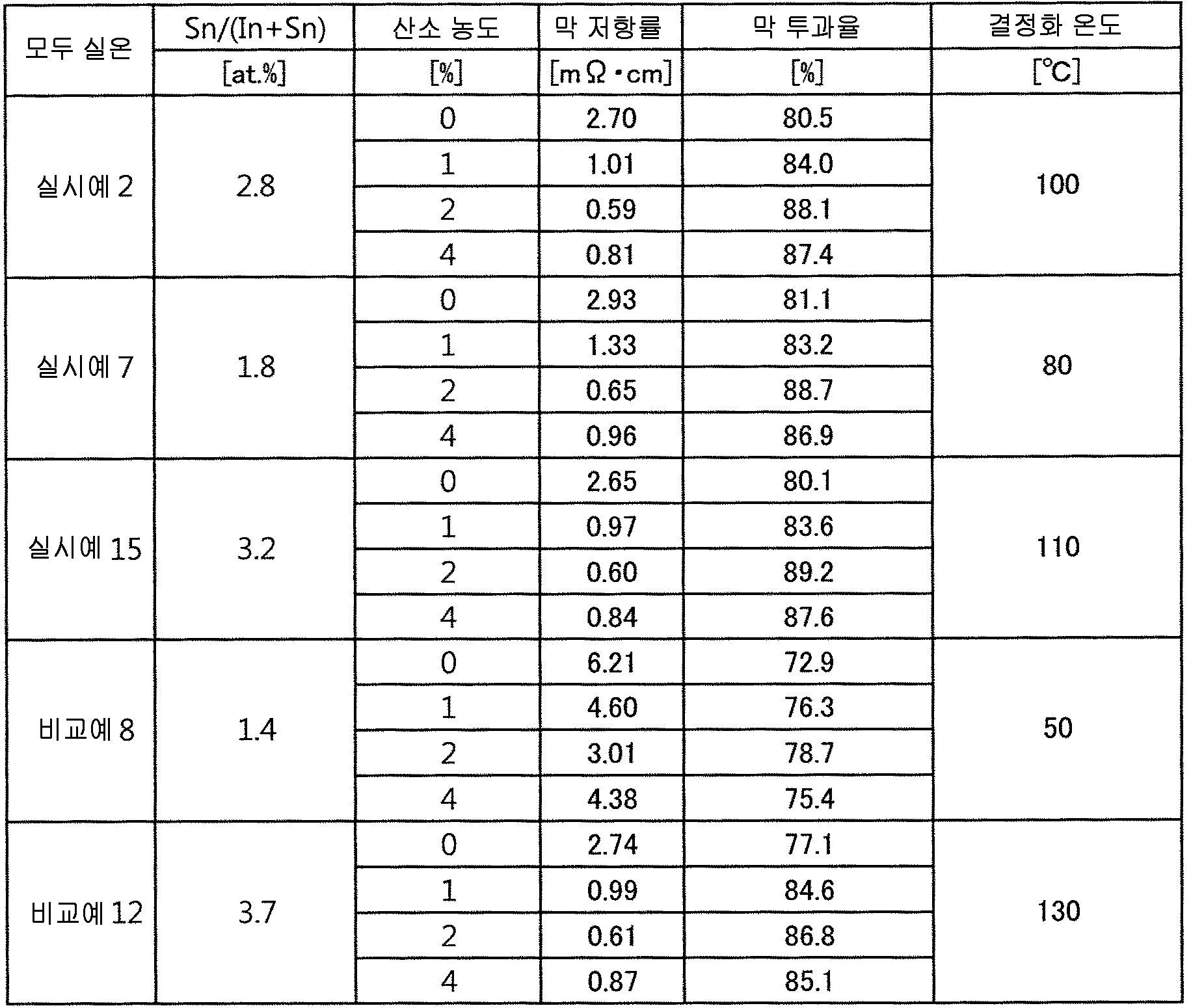
이 실시예 2 에 대하여, 동일한 DC 파워 밀도, 가스압으로, 스퍼터 가스에 아르곤과, 산소 함유량을 0, 1, 2, 4 % 로 하고, 가스 유량 300 sccm 으로 유리 기판 (EagleXG) 에 무가열로 성막하여, 40 ㎚ 의 ITO 막을 제작하였다.In Example 2, the same DC power density and gas pressure were applied to the glass substrate (Eagle XG) at a gas flow rate of 300 sccm with argon and oxygen at 0, 1, 2, and 4% Thus, a 40 nm ITO film was formed.
이 막을, 이너트 오븐노 (형번 : INL-45-S) 를 사용하여, 50 ∼ 200 ℃ 까지 대기 분위기에서 60 분 가열하고, 가열 전후의 막을 XRD (장치 형번 : 리가쿠 제조_전자동 수평형 다목적 X 선 회절 장치 SmartLab) 측정으로 결정화의 유무를 확인하였다. 결정화 온도는, XRD 측정으로 In2O3 의 (222) 면의 피크가 확인된 온도로 하였다.This film was heated to 50 to 200 ° C in an atmospheric environment for 60 minutes using an inert oven furnace (model number INL-45-S), and the film before and after heating was subjected to XRD (apparatus model number: Rigaku Co., X-ray diffractometer SmartLab). The crystallization temperature was set to a temperature at which a peak of (222) plane of In 2 O 3 was confirmed by XRD measurement.
산소 농도가 0 % 인 경우, 막 저항률은 2.70 mΩ·㎝, 500 ㎚ 파장에서의 투과율은 80.5 %, 결정화 온도는 100 ℃ 였다.When the oxygen concentration was 0%, the film resistivity was 2.70 m? 占. M, the transmittance at 500 nm wavelength was 80.5%, and the crystallization temperature was 100 占 폚.
산소 농도가 1 % 인 경우, 막 저항률은 1.01 mΩ·㎝, 500 ㎚ 파장에서의 투과율은 84.0 %, 결정화 온도는 100 ℃ 였다.When the oxygen concentration was 1%, the film resistivity was 1.01 m? 占. M, the transmittance at a wavelength of 500 nm was 84.0%, and the crystallization temperature was 100 占 폚.
산소 농도가 2 % 인 경우, 막 저항률은 0.59 mΩ·㎝, 500 ㎚ 파장에서의 투과율은 88.1 %, 결정화 온도는 100 ℃ 였다.When the oxygen concentration was 2%, the film resistivity was 0.59 m? 占. M, the transmittance at a wavelength of 500 nm was 88.1%, and the crystallization temperature was 100 占 폚.
산소 농도가 4 % 인 경우, 막 저항률은 0.81 mΩ·㎝, 500 ㎚ 파장에서의 투과율은 87.4 %, 결정화 온도는 100 ℃ 였다.When the oxygen concentration was 4%, the film resistivity was 0.81 m? 占. M, the transmittance at a wavelength of 500 nm was 87.4%, and the crystallization temperature was 100 占 폚.
이 결과를, 표 2 에 나타낸다. 모두, 양호한 결과가 얻어졌다.The results are shown in Table 2. All, good results were obtained.
(실시예 3)(Example 3)
원자비로 Sn/(In + Sn) 이, 2.8 % 가 되도록 비율을 조정한 SnO2 분말과 In2O3 분말을 소결 원료로서 사용하여 산소 분위기 중에서 소결하였다. 최고 소결 온도를 1450 ℃ 로 하고, 최고 소결 온도에서의 유지 시간을 15 시간으로 하였다. 그 후, 강온 냉각시에 1370 ℃ 에서 1 시간 유지하였다. 이렇게 하여 얻어진 소결체는, 소결체 밀도 7.105 g/㎤, 굽힘 강도 121 ㎫, 벌크 저항률 0.124 mΩ·㎝, 평균 결정 입경 3.66 ㎛, 산화주석 리치상의 면적률 0.35 %, 산화주석 리치상 삼중점 존재 확률 99 %, 공공 면적률은 0.05 % 였다.SnO 2 powder and In 2 O 3 powder whose ratios were adjusted so that Sn / (In + Sn) was 2.8% in terms of atomic ratio were sintered in an oxygen atmosphere as raw materials for sintering. The maximum sintering temperature was 1450 ° C and the holding time at the maximum sintering temperature was 15 hours. Thereafter, it was held at 1370 캜 for one hour during cooling down by cooling. The sintered body thus obtained had a sintered body density of 7.105 g / cm3, a bending strength of 121 MPa, a bulk resistivity of 0.124 m? 占, m, an average crystal grain size of 3.66 占 퐉, an area ratio of 0.35% on a tin oxide rich phase, The public area rate was 0.05%.
이 소결체를 사용하여 타겟을 제작하고, DC 파워 밀도 2.3 W/㎠, 가스압은 0.6 ㎩, 스퍼터 가스는 아르곤 (Ar), 가스 유량 300 sccm 으로 연속적으로 35 시간 스퍼터링을 실시한 결과, 아킹 발생 횟수는 20 회/24 hr, 노듈 피복률은 0.3 % 로 양호하였다.The sputtering was continuously performed for 35 hours at a DC power density of 2.3 W / cm 2, a gas pressure of 0.6 Pa, a sputter gas of argon (Ar), and a gas flow rate of 300 sccm. As a result, Times / 24 hr, and the nodule coverage rate was 0.3%.
(실시예 4)(Example 4)
원자비로 Sn/(In + Sn) 이, 2.8 % 가 되도록 비율을 조정한 SnO2 분말과 In2O3 분말을 소결 원료로서 사용하여 산소 분위기 중에서 소결하였다. 최고 소결 온도를 1430 ℃ 로 하고, 최고 소결 온도에서의 유지 시간을 10 시간으로 하였다. 그 후, 강온 냉각시에 1330 ℃ 에서 1 시간 유지하였다. 이렇게 하여 얻어진 소결체는, 소결체 밀도 7.082 g/㎤, 굽힘 강도 116 ㎫, 벌크 저항률 0.118 mΩ·㎝, 평균 결정 입경 3.26 ㎛, 산화주석 리치상의 면적률 0.68 %, 산화주석 리치상 삼중점 존재 확률 99 %, 공공 면적률은 0.10 % 였다.SnO 2 powder and In 2 O 3 powder whose ratios were adjusted so that Sn / (In + Sn) was 2.8% in terms of atomic ratio were sintered in an oxygen atmosphere as raw materials for sintering. The maximum sintering temperature was 1430 ° C and the holding time at the maximum sintering temperature was 10 hours. Thereafter, the temperature was maintained at 1330 캜 for one hour during cooling down. The sintered body thus obtained had a sintered body density of 7.082 g / cm3, a bending strength of 116 Mpa, a bulk resistivity of 0.118 m? 占, m, an average crystal grain size of 3.26 占 퐉, an area ratio of 0.98% on a tin oxide rich phase, The public area rate was 0.10%.
이 소결체를 사용하여 타겟을 제작하고, DC 파워 밀도 2.3 W/㎠, 가스압은 0.6 ㎩, 스퍼터 가스는 아르곤 (Ar), 가스 유량 300 sccm 으로 연속적으로 35 시간 스퍼터링을 실시한 결과, 아킹 발생 횟수는 25 회/24 hr, 노듈 피복률은 0.7 % 로 양호하였다.The sputtering was performed continuously for 35 hours at a DC power density of 2.3 W / cm 2, a gas pressure of 0.6 Pa, a sputter gas of argon (Ar) and a gas flow rate of 300 sccm for 35 hours. As a result, Times / 24 hr, and the nodule coverage rate was 0.7%.
(실시예 5)(Example 5)
원자비로 Sn/(In + Sn) 이, 2.8 % 가 되도록 비율을 조정한 SnO2 분말과 In2O3 분말을 소결 원료로서 사용하여 산소 분위기 중에서 소결하였다. 최고 소결 온도를 1400 ℃ 로 하고, 최고 소결 온도에서의 유지 시간을 10 시간으로 하였다. 그 후, 강온 냉각시에 1300 ℃ 에서 1 시간 유지하였다. 이렇게 하여 얻어진 소결체는, 소결체 밀도 7.058 g/㎤, 굽힘 강도 113 ㎫, 벌크 저항률 0.121 mΩ·㎝, 평균 결정 입경 3.20 ㎛, 산화주석 리치상의 면적률 0.83 %, 산화주석 리치상 삼중점 존재 확률 98 %, 공공 면적률은 0.15 % 였다.SnO 2 powder and In 2 O 3 powder whose ratios were adjusted so that Sn / (In + Sn) was 2.8% in terms of atomic ratio were sintered in an oxygen atmosphere as raw materials for sintering. The maximum sintering temperature was 1400 캜, and the retention time at the maximum sintering temperature was 10 hours. Thereafter, it was held at 1300 占 폚 for one hour at the time of cold cooling. The sintered body thus obtained had a sintered body density of 7.058 g / cm 3, a bending strength of 113 MPa, a bulk resistivity of 0.121 m? 占, m, an average crystal grain size of 3.20 占 퐉, an area ratio of 0.83% on a tin oxide rich phase, The public area rate was 0.15%.
이 소결체를 사용하여 타겟을 제작하고, DC 파워 밀도 2.3 W/㎠, 가스압은 0.6 ㎩, 스퍼터 가스는 아르곤 (Ar), 가스 유량 300 sccm 으로 연속적으로 35 시간 스퍼터링을 실시한 결과, 아킹 발생 횟수는 31 회/24 hr, 노듈 피복률은 1.2 % 로 양호하였다.The sputtering was carried out continuously for 35 hours at a DC power density of 2.3 W / cm 2, a gas pressure of 0.6 Pa, a sputter gas of argon (Ar) and a gas flow rate of 300 sccm for 35 hours. As a result, Times / 24 hr, and the nodule coverage rate was 1.2%.
(실시예 6)(Example 6)
원자비로 Sn/(In + Sn) 이, 1.8 % 가 되도록 비율을 조정한 SnO2 분말과 In2O3 분말을 소결 원료로서 사용하여 산소 분위기 중에서 소결하였다. 최고 소결 온도를 1350 ℃ 로 하고, 최고 소결 온도에서의 유지 시간을 10 시간으로 하였다. 그 후, 강온 냉각시에 1250 ℃ 에서 1 시간 유지하였다. 이렇게 하여 얻어진 소결체는, 소결체 밀도 7.036 g/㎤, 굽힘 강도 110 ㎫, 벌크 저항률 0.129 mΩ·㎝, 평균 결정 입경 3.01 ㎛, 산화주석 리치상의 면적률 0.95 %, 산화주석 리치상 삼중점 존재 확률 97 %, 공공 면적률은 0.23 % 였다.SnO 2 powder and In 2 O 3 powder whose ratios were adjusted so that Sn / (In + Sn) was 1.8% in terms of atomic ratio were sintered in an oxygen atmosphere as raw materials for sintering. The maximum sintering temperature was 1350 ° C and the holding time at the maximum sintering temperature was 10 hours. Thereafter, it was held at 1250 占 폚 for one hour during cold cooling. The sintered body thus obtained had a sintered body density of 7.036 g / cm 3, a bending strength of 110 MPa, a bulk resistivity of 0.129 m? 占, m, an average crystal grain size of 3.01 占 퐉, an area ratio of 0.95% on the tin oxide rich phase, The public area rate was 0.23%.
이 소결체를 사용하여 타겟을 제작하고, DC 파워 밀도 2.3 W/㎠, 가스압은 0.6 ㎩, 스퍼터 가스는 아르곤 (Ar), 가스 유량 300 sccm 으로 연속적으로 35 시간 스퍼터링을 실시한 결과, 아킹 발생 횟수는 40 회/24 hr, 노듈 피복률은 1.5 % 로 양호하였다.As a result of sputtering for 35 hours at a DC power density of 2.3 W / cm 2, a gas pressure of 0.6 Pa, a sputter gas of argon (Ar) and a gas flow rate of 300 sccm for 35 hours, Times / 24 hr and the nodule coverage rate was 1.5%.
(실시예 7)(Example 7)
원자비로 Sn/(In + Sn) 이, 1.8 % 가 되도록 비율을 조정한 SnO2 분말과 In2O3 분말을 소결 원료로서 사용하여 산소 분위기 중에서 소결하였다. 최고 소결 온도를 1450 ℃ 로 하고, 최고 소결 온도에서의 유지 시간을 10 시간으로 하였다. 그 후, 강온 냉각시에 1350 ℃ 에서 1 시간 유지하였다. 이렇게 하여 얻어진 소결체는, 소결체 밀도 7.074 g/㎤, 굽힘 강도 111 ㎫, 벌크 저항률 0.131 mΩ·㎝, 평균 결정 입경 3.96 ㎛, 산화주석 리치상의 면적률 0.21 %, 산화주석 리치상 삼중점 존재 확률 99 %, 공공 면적률은 0.08 % 였다.SnO 2 powder and In 2 O 3 powder whose ratios were adjusted so that Sn / (In + Sn) was 1.8% in terms of atomic ratio were sintered in an oxygen atmosphere as raw materials for sintering. The maximum sintering temperature was 1450 ° C and the holding time at the maximum sintering temperature was 10 hours. Thereafter, it was held at 1350 ° C for one hour during cooling down by cooling. The sintered body thus obtained had a sintered body density of 7.074 g / cm 3, a bending strength of 111 MPa, a bulk resistivity of 0.131 m? 占, m, an average crystal grain size of 3.96 占 퐉, an area ratio of 0.21% on a tin oxide rich phase, The public area rate was 0.08%.
이 소결체를 사용하여 타겟을 제작하고, DC 파워 밀도 2.3 W/㎠, 가스압은 0.6 ㎩, 스퍼터 가스는 아르곤 (Ar), 가스 유량 300 sccm 으로 연속적으로 35 시간 스퍼터링을 실시한 결과, 아킹 발생 횟수는 31 회/24 hr, 노듈 피복률은 0.9 % 로 양호하였다.The sputtering was carried out continuously for 35 hours at a DC power density of 2.3 W / cm 2, a gas pressure of 0.6 Pa, a sputter gas of argon (Ar) and a gas flow rate of 300 sccm for 35 hours. As a result, Times / 24 hr, and the nodule coverage rate was 0.9%.
이 실시예 7 에 대하여, 동일한 DC 파워 밀도, 가스압으로, 스퍼터 가스에 아르곤과, 산소 함유량을 0, 1, 2, 4 % 로 하고, 가스 유량 300 sccm 으로 유리 기판 (EagleXG) 에 무가열로 성막하여, 40 ㎚ 의 ITO 막을 제작하였다.In Example 7, the same DC power density and gas pressure were applied to the glass substrate (Eagle XG) at a gas flow rate of 300 sccm with argon and oxygen at 0, 1, 2, and 4% Thus, a 40 nm ITO film was formed.
이 막을, 이너트 오븐노 (형번 : INL-45-S) 를 사용하여, 50 ∼ 200 ℃ 까지 대기 분위기에서 60 분 가열하고, 가열 전후의 막을 XRD (장치 형번 : 리가쿠 제조_전자동 수평형 다목적 X 선 회절 장치 SmartLab) 측정으로 결정화의 유무를 확인하였다. 결정화 온도는, XRD 측정으로 In2O3 의 (222) 면의 피크가 확인된 온도로 하였다.This film was heated to 50 to 200 ° C in an atmospheric environment for 60 minutes using an inert oven furnace (model number INL-45-S), and the film before and after heating was subjected to XRD (apparatus model number: Rigaku Co., X-ray diffractometer SmartLab). The crystallization temperature was set to a temperature at which a peak of (222) plane of In 2 O 3 was confirmed by XRD measurement.
산소 농도가 0 % 인 경우, 막 저항률은 2.93 mΩ·㎝, 500 ㎚ 파장에서의 투과율은 81.1 %, 결정화 온도는 80 ℃ 였다.When the oxygen concentration was 0%, the film resistivity was 2.93 m? 占. M, the transmittance at a wavelength of 500 nm was 81.1%, and the crystallization temperature was 80 占 폚.
산소 농도가 1 % 인 경우, 막 저항률은 1.33 mΩ·㎝, 500 ㎚ 파장에서의 투과율은 83.2 %, 결정화 온도는 80 ℃ 였다.When the oxygen concentration was 1%, the film resistivity was 1.33 m? 占. M, the transmittance at a wavelength of 500 nm was 83.2%, and the crystallization temperature was 80 占 폚.
산소 농도가 2 % 인 경우, 막 저항률은 0.65 mΩ·㎝, 500 ㎚ 파장에서의 투과율은 88.7 %, 결정화 온도는 80 ℃ 였다.When the oxygen concentration was 2%, the film resistivity was 0.65 m? 占. M, the transmittance at a wavelength of 500 nm was 88.7%, and the crystallization temperature was 80 占 폚.
산소 농도가 4 % 인 경우, 막 저항률은 0.96 mΩ·㎝, 500 ㎚ 파장에서의 투과율은 86.9 %, 결정화 온도는 80 ℃ 였다.When the oxygen concentration was 4%, the film resistivity was 0.96 m? 占. M, the transmittance at a wavelength of 500 nm was 86.9%, and the crystallization temperature was 80 占 폚.
이 결과를, 마찬가지로 표 2 에 나타낸다. 모두, 양호한 결과가 얻어졌다.The results are also shown in Table 2. All, good results were obtained.
(실시예 8)(Example 8)
원자비로 Sn/(In + Sn) 이, 1.8 % 가 되도록 비율을 조정한 SnO2 분말과 In2O3 분말을 소결 원료로서 사용하여 산소 분위기 중에서 소결하였다. 최고 소결 온도를 1400 ℃ 로 하고, 최고 소결 온도에서의 유지 시간을 10 시간으로 하였다. 그 후, 강온 냉각시에 1300 ℃ 에서 1 시간 유지하였다. 이렇게 하여 얻어진 소결체는, 소결체 밀도 7.045 g/㎤, 굽힘 강도 107 ㎫, 벌크 저항률 0.125 mΩ·㎝, 평균 결정 입경 3.46 ㎛, 산화주석 리치상의 면적률 0.26 %, 산화주석 리치상 삼중점 존재 확률 99 %, 공공 면적률은 0.11 % 였다.SnO 2 powder and In 2 O 3 powder whose ratios were adjusted so that Sn / (In + Sn) was 1.8% in terms of atomic ratio were sintered in an oxygen atmosphere as raw materials for sintering. The maximum sintering temperature was 1400 캜, and the retention time at the maximum sintering temperature was 10 hours. Thereafter, it was held at 1300 占 폚 for one hour at the time of cold cooling. The sintered body thus obtained had a sintered body density of 7.045 g / cm3, a bending strength of 107 MPa, a bulk resistivity of 0.125 m? 占, m, an average crystal grain size of 3.46 占 퐉, an area ratio of 0.26% on a tin oxide rich phase, The public area rate was 0.11%.
이 소결체를 사용하여 타겟을 제작하고, DC 파워 밀도 2.3 W/㎠, 가스압은 0.6 ㎩, 스퍼터 가스는 아르곤 (Ar), 가스 유량 300 sccm 으로 연속적으로 35 시간 스퍼터링을 실시한 결과, 아킹 발생 횟수는 33 회/24 hr, 노듈 피복률은 1.2 % 로 양호하였다.As a result of sputtering for 35 hours at a DC power density of 2.3 W / cm 2, a gas pressure of 0.6 Pa, a sputter gas of argon (Ar) and a gas flow rate of 300 sccm for 35 hours, the number of arcing occurrences was 33 Times / 24 hr, and the nodule coverage rate was 1.2%.
(실시예 9)(Example 9)
원자비로 Sn/(In + Sn) 이, 2.1 % 가 되도록 비율을 조정한 SnO2 분말과 In2O3 분말을 소결 원료로서 사용하여 산소 분위기 중에서 소결하였다. 최고 소결 온도를 1450 ℃ 로 하고, 최고 소결 온도에서의 유지 시간을 10 시간으로 하였다. 그 후, 강온 냉각시에 1350 ℃ 에서 1 시간 유지하였다. 이렇게 하여 얻어진 소결체는, 소결체 밀도 7.079 g/㎤, 굽힘 강도 113 ㎫, 벌크 저항률 0.125 mΩ·㎝, 평균 결정 입경 3.55 ㎛, 산화주석 리치상의 면적률 0.18 %, 산화주석 리치상 삼중점 존재 확률 99 %, 공공 면적률은 0.12 % 였다.SnO 2 powder and In 2 O 3 powder whose ratios were adjusted so that Sn / (In + Sn) was 2.1% in terms of atomic ratio were sintered in an oxygen atmosphere using as raw materials for sintering. The maximum sintering temperature was 1450 ° C and the holding time at the maximum sintering temperature was 10 hours. Thereafter, it was held at 1350 ° C for one hour during cooling down by cooling. The sintered body thus obtained had a sintered body density of 7.079 g / cm 3, a bending strength of 113 MPa, a bulk resistivity of 0.125 m? 占, m, an average crystal grain size of 3.55 占 퐉, an area ratio of 0.18% on a tin oxide rich phase, The public area rate was 0.12%.
이 소결체를 사용하여 타겟을 제작하고, DC 파워 밀도 2.3 W/㎠, 가스압은 0.6 ㎩, 스퍼터 가스는 아르곤 (Ar), 가스 유량 300 sccm 으로 연속적으로 35 시간 스퍼터링을 실시한 결과, 아킹 발생 횟수는 30 회/24 hr, 노듈 피복률은 1.3 % 로 양호하였다.The sputtering was carried out continuously for 35 hours at a DC power density of 2.3 W / cm 2, a gas pressure of 0.6 Pa, a sputter gas of argon (Ar) and a gas flow rate of 300 sccm for 35 hours. As a result, Times / 24 hr, and the nodule coverage rate was 1.3%.
(실시예 10)(Example 10)
원자비로 Sn/(In + Sn) 이, 2.1 % 가 되도록 비율을 조정한 SnO2 분말과 In2O3 분말을 소결 원료로서 사용하여 산소 분위기 중에서 소결하였다. 최고 소결 온도를 1400 ℃ 로 하고, 최고 소결 온도에서의 유지 시간을 10 시간으로 하였다. 그 후, 강온 냉각시에 1300 ℃ 에서 1 시간 유지하였다. 이렇게 하여 얻어진 소결체는, 소결체 밀도 7.050 g/㎤, 굽힘 강도 110 ㎫, 벌크 저항률 0.122 mΩ·㎝, 평균 결정 입경 2.75 ㎛, 산화주석 리치상의 면적률 0.22 %, 산화주석 리치상 삼중점 존재 확률 99 %, 공공 면적률은 0.13 % 였다.SnO 2 powder and In 2 O 3 powder whose ratios were adjusted so that Sn / (In + Sn) was 2.1% in terms of atomic ratio were sintered in an oxygen atmosphere using as raw materials for sintering. The maximum sintering temperature was 1400 캜, and the retention time at the maximum sintering temperature was 10 hours. Thereafter, it was held at 1300 占 폚 for one hour at the time of cold cooling. The sintered body thus obtained had a sintered body density of 7.050 g / cm 3, a bending strength of 110 MPa, a bulk resistivity of 0.122 m? 占, m, an average crystal grain size of 2.75 占 퐉, an area ratio of 0.22% on a tin oxide rich phase, The public area rate was 0.13%.
이 소결체를 사용하여 타겟을 제작하고, DC 파워 밀도 2.3 W/㎠, 가스압은 0.6 ㎩, 스퍼터 가스는 아르곤 (Ar), 가스 유량 300 sccm 으로 연속적으로 35 시간 스퍼터링을 실시한 결과, 아킹 발생 횟수는 31 회/24 hr, 노듈 피복률은 1.6 % 로 양호하였다.The sputtering was carried out continuously for 35 hours at a DC power density of 2.3 W / cm 2, a gas pressure of 0.6 Pa, a sputter gas of argon (Ar) and a gas flow rate of 300 sccm for 35 hours. As a result, Times / 24 hr, and the nodule coverage rate was 1.6%.
(실시예 11)(Example 11)
원자비로 Sn/(In + Sn) 이, 2.6 % 가 되도록 비율을 조정한 SnO2 분말과 In2O3 분말을 소결 원료로서 사용하여 산소 분위기 중에서 소결하였다. 최고 소결 온도를 1450 ℃ 로 하고, 최고 소결 온도에서의 유지 시간을 10 시간으로 하였다. 그 후, 강온 냉각시에 1350 ℃ 에서 1 시간 유지하였다. 이렇게 하여 얻어진 소결체는, 소결체 밀도 7.088 g/㎤, 굽힘 강도 119 ㎫, 벌크 저항률 0.123 mΩ·㎝, 평균 결정 입경 2.97 ㎛, 산화주석 리치상의 면적률 0.33 %, 산화주석 리치상 삼중점 존재 확률 98 %, 공공 면적률은 0.10 % 였다.SnO 2 powder and In 2 O 3 powder whose ratios were adjusted so that Sn / (In + Sn) was 2.6% in terms of atomic ratio were sintered in an oxygen atmosphere as raw materials for sintering. The maximum sintering temperature was 1450 ° C and the holding time at the maximum sintering temperature was 10 hours. Thereafter, it was held at 1350 ° C for one hour during cooling down by cooling. The sintered body thus obtained had a sintered body density of 7.088 g / cm3, a bending strength of 119 Mpa, a bulk resistivity of 0.123 m? 占, m, an average crystal grain size of 2.97 占 퐉, an area ratio of 0.33% on a tin oxide rich phase, The public area rate was 0.10%.
이 소결체를 사용하여 타겟을 제작하고, DC 파워 밀도 2.3 W/㎠, 가스압은 0.6 ㎩, 스퍼터 가스는 아르곤 (Ar), 가스 유량 300 sccm 으로 연속적으로 35 시간 스퍼터링을 실시한 결과, 아킹 발생 횟수는 25 회/24 hr, 노듈 피복률은 1 % 로 양호하였다.The sputtering was performed continuously for 35 hours at a DC power density of 2.3 W / cm 2, a gas pressure of 0.6 Pa, a sputter gas of argon (Ar) and a gas flow rate of 300 sccm for 35 hours. As a result, Times / 24 hr, and the nodule coverage rate was 1%.
(실시예 12)(Example 12)
원자비로 Sn/(In + Sn) 이, 2.6 % 가 되도록 비율을 조정한 SnO2 분말과 In2O3 분말을 소결 원료로서 사용하여 산소 분위기 중에서 소결하였다. 최고 소결 온도를 1400 ℃ 로 하고, 최고 소결 온도에서의 유지 시간을 10 시간으로 하였다. 그 후, 강온 냉각시에 1300 ℃ 에서 1 시간 유지하였다. 이렇게 하여 얻어진 소결체는, 소결체 밀도 7.071 g/㎤, 굽힘 강도 115 ㎫, 벌크 저항률 0.119 mΩ·㎝, 평균 결정 입경 2.83 ㎛, 산화주석 리치상의 면적률 0.38 %, 산화주석 리치상 삼중점 존재 확률 98 %, 공공 면적률은 0.10 % 였다.SnO 2 powder and In 2 O 3 powder whose ratios were adjusted so that Sn / (In + Sn) was 2.6% in terms of atomic ratio were sintered in an oxygen atmosphere as raw materials for sintering. The maximum sintering temperature was 1400 캜, and the retention time at the maximum sintering temperature was 10 hours. Thereafter, it was held at 1300 占 폚 for one hour at the time of cold cooling. The sintered body thus obtained had a sintered body density of 7.071 g / cm3, a bending strength of 115 MPa, a bulk resistivity of 0.119 m? 占, m, an average crystal grain size of 2.83 占 퐉, an area ratio of 0.38% on a tin oxide rich phase, The public area rate was 0.10%.
이 소결체를 사용하여 타겟을 제작하고, DC 파워 밀도 2.3 W/㎠, 가스압은 0.6 ㎩, 스퍼터 가스는 아르곤 (Ar), 가스 유량 300 sccm 으로 연속적으로 35 시간 스퍼터링을 실시한 결과, 아킹 발생 횟수는 28 회/24 hr, 노듈 피복률은 1.1 % 로 양호하였다.The sputtering was carried out continuously for 35 hours at a DC power density of 2.3 W / cm 2, a gas pressure of 0.6 Pa, a sputter gas of argon (Ar) and a gas flow rate of 300 sccm for 35 hours. As a result, Times / 24 hr, and the nodule coverage rate was 1.1%.
(실시예 13)(Example 13)
원자비로 Sn/(In + Sn) 이, 3.0 % 가 되도록 비율을 조정한 SnO2 분말과 In2O3 분말을 소결 원료로서 산소 분위기 중에서 사용하여 소결하였다. 최고 소결 온도를 1450 ℃ 로 하고, 최고 소결 온도에서의 유지 시간을 10 시간으로 하였다. 그 후, 강온 냉각시에 1350 ℃ 에서 1 시간 유지하였다. 이렇게 하여 얻어진 소결체는, 소결체 밀도 7.103 g/㎤, 굽힘 강도 126 ㎫, 벌크 저항률 0.117 mΩ·㎝, 평균 결정 입경 3.67 ㎛, 산화주석 리치상의 면적률 0.41 %, 산화주석 리치상 삼중점 존재 확률 98 %, 공공 면적률은 0.08 % 였다.SnO 2 powder and In 2 O 3 powder whose ratios were adjusted so that Sn / (In + Sn) was 3.0% in atomic ratio were sintered in an oxygen atmosphere as a raw material for sintering. The maximum sintering temperature was 1450 ° C and the holding time at the maximum sintering temperature was 10 hours. Thereafter, it was held at 1350 ° C for one hour during cooling down by cooling. The sintered body thus obtained had a sintered body density of 7.103 g / cm 3, a bending strength of 126 MPa, a bulk resistivity of 0.117 m? 占, m, an average crystal grain size of 3.67 占 퐉, an area ratio of 0.41% on a tin oxide rich phase, The public area rate was 0.08%.
이 소결체를 사용하여 타겟을 제작하고, DC 파워 밀도 2.3 W/㎠, 가스압은 0.6 ㎩, 스퍼터 가스는 아르곤 (Ar), 가스 유량 300 sccm 으로 연속적으로 35 시간 스퍼터링을 실시한 결과, 아킹 발생 횟수는 21 회/24 hr, 노듈 피복률은 0.9 % 로 양호하였다.The sputtering was continuously performed for 35 hours at a DC power density of 2.3 W / cm 2, a gas pressure of 0.6 Pa, a sputter gas of argon (Ar), and a gas flow rate of 300 sccm. As a result, Times / 24 hr, and the nodule coverage rate was 0.9%.
(실시예 14)(Example 14)
원자비로 Sn/(In + Sn) 이, 3.0 % 가 되도록 비율을 조정한 SnO2 분말과 In2O3 분말을 소결 원료로서 사용하여 산소 분위기 중에서 소결하였다. 최고 소결 온도를 1400 ℃ 로 하고, 최고 소결 온도에서의 유지 시간을 10 시간으로 하였다. 그 후, 강온 냉각시에 1300 ℃ 에서 1 시간 유지하였다. 이렇게 하여 얻어진 소결체는, 소결체 밀도 7.091 g/㎤, 굽힘 강도 121 ㎫, 벌크 저항률 0.115 mΩ·㎝, 평균 결정 입경 3.49 ㎛, 산화주석 리치상의 면적률 0.46 %, 산화주석 리치상 삼중점 존재 확률 98 %, 공공 면적률은 0.09 % 였다.SnO 2 powder and In 2 O 3 powder whose ratios were adjusted so that Sn / (In + Sn) was 3.0% in terms of atomic ratio were sintered in an oxygen atmosphere using as raw materials for sintering. The maximum sintering temperature was 1400 캜, and the retention time at the maximum sintering temperature was 10 hours. Thereafter, it was held at 1300 占 폚 for one hour at the time of cold cooling. The sintered body thus obtained had a sintered body density of 7.091 g / cm3, a bending strength of 121 MPa, a bulk resistivity of 0.115 m? 占, m, an average crystal grain size of 3.49 占 퐉, an area ratio of 0.40% on a tin oxide rich phase, The public area rate was 0.09%.
이 소결체를 사용하여 타겟을 제작하고, DC 파워 밀도 2.3 W/㎠, 가스압은 0.6 ㎩, 스퍼터 가스는 아르곤 (Ar), 가스 유량 300 sccm 으로 연속적으로 35 시간 스퍼터링을 실시한 결과, 아킹 발생 횟수는 24 회/24 hr, 노듈 피복률은 0.9 % 로 양호하였다.The sputtering was performed continuously for 35 hours at a DC power density of 2.3 W / cm 2, a gas pressure of 0.6 Pa, a sputter gas of argon (Ar) and a gas flow rate of 300 sccm for 35 hours. As a result, Times / 24 hr, and the nodule coverage rate was 0.9%.
(실시예 15)(Example 15)
원자비로 Sn/(In + Sn) 이, 3.2 % 가 되도록 비율을 조정한 SnO2 분말과 In2O3 분말을 소결 원료로서 사용하여 산소 분위기 중에서 소결하였다. 최고 소결 온도를 1450 ℃ 로 하고, 최고 소결 온도에서의 유지 시간을 10 시간으로 하였다. 그 후, 강온 냉각시에 1350 ℃ 에서 1 시간 유지하였다. 이렇게 하여 얻어진 소결체는, 소결체 밀도 7.109 g/㎤, 굽힘 강도 127 ㎫, 벌크 저항률 0.110 mΩ·㎝, 평균 결정 입경 3.82 ㎛, 산화주석 리치상의 면적률 0.55 %, 산화주석 리치상 삼중점 존재 확률 98 %, 공공 면적률은 0.07 % 였다.SnO 2 powder and In 2 O 3 powder whose ratios were adjusted so that Sn / (In + Sn) was 3.2% in terms of atomic ratio were sintered in an oxygen atmosphere using as raw materials for sintering. The maximum sintering temperature was 1450 ° C and the holding time at the maximum sintering temperature was 10 hours. Thereafter, it was held at 1350 ° C for one hour during cooling down by cooling. The sintered body thus obtained had a sintered body density of 7.109 g / cm 3, a bending strength of 127 MPa, a bulk resistivity of 0.110 m? 占, m, an average crystal grain size of 3.82 占 퐉, an area ratio of 0.55% on a tin oxide rich phase, The public area rate was 0.07%.
이 소결체를 사용하여 타겟을 제작하고, DC 파워 밀도 2.3 W/㎠, 가스압은 0.6 ㎩, 스퍼터 가스는 아르곤 (Ar), 가스 유량 300 sccm 으로 연속적으로 35 시간 스퍼터링을 실시한 결과, 아킹 발생 횟수는 18 회/24 hr, 노듈 피복률은 0.7 % 로 양호하였다.The sputtering was performed continuously for 35 hours at a DC power density of 2.3 W / cm 2, a gas pressure of 0.6 Pa, a sputter gas of argon (Ar) and a gas flow rate of 300 sccm for 35 hours. As a result, Times / 24 hr, and the nodule coverage rate was 0.7%.
이 실시예 15 에 대하여, 동일한 DC 파워 밀도, 가스압으로, 스퍼터 가스에 아르곤과, 산소 함유량을 0, 1, 2, 4 % 로 하고, 가스 유량 300 sccm 으로 유리 기판 (EagleXG) 에 무가열로 성막하여, 40 ㎚ 의 ITO 막을 제작하였다.In Example 15, the same DC power density and gas pressure were used as the sputter gas, and argon was added to the glass substrate (Eagle XG) at a gas flow rate of 300 sccm with no oxygen at 0, 1, 2, and 4% Thus, a 40 nm ITO film was formed.
이 막을, 이너트 오븐노 (형번 : INL-45-S) 를 사용하여, 50 ∼ 200 ℃ 까지 대기 분위기에서 60 분 가열하여, 가열 전후의 막을 XRD (장치 형번 : 리가쿠 제조_전자동 수평형 다목적 X 선 회절 장치 SmartLab) 측정으로 결정화의 유무를 확인하였다. 결정화 온도는, XRD 측정으로 In2O3 의 (222) 면의 피크가 확인된 온도로 하였다.This film was heated to 50 to 200 ° C in an atmospheric environment for 60 minutes using an inert oven furnace (model number INL-45-S), and the film before and after heating was subjected to XRD (apparatus model number: Rigaku Co., X-ray diffractometer SmartLab). The crystallization temperature was set to a temperature at which a peak of (222) plane of In 2 O 3 was confirmed by XRD measurement.
산소 농도가 0 % 인 경우, 막 저항률은 2.65 mΩ·㎝, 500 ㎚ 파장에서의 투과율은 80.1 %, 결정화 온도는 110 ℃ 였다.When the oxygen concentration was 0%, the film resistivity was 2.65 m? 占. M, the transmittance at a wavelength of 500 nm was 80.1%, and the crystallization temperature was 110 占 폚.
산소 농도가 1 % 인 경우, 막 저항률은 0.97 mΩ·㎝, 500 ㎚ 파장에서의 투과율은 83.6 %, 결정화 온도는 110 ℃ 였다.When the oxygen concentration was 1%, the film resistivity was 0.97 m? 占. M, the transmittance at a wavelength of 500 nm was 83.6%, and the crystallization temperature was 110 占 폚.
산소 농도가 2 % 인 경우, 막 저항률은 0.60 mΩ·㎝, 500 ㎚ 파장에서의 투과율은 89.2 %, 결정화 온도는 110 ℃ 였다.When the oxygen concentration was 2%, the film resistivity was 0.60 m? 占. M, the transmittance at 500 nm wavelength was 89.2%, and the crystallization temperature was 110 占 폚.
산소 농도가 4 % 인 경우, 막 저항률은 0.84 mΩ·㎝, 500 ㎚ 파장에서의 투과율은 87.6 %, 결정화 온도는 110 ℃ 였다.When the oxygen concentration was 4%, the film resistivity was 0.84 m? 占. M, the transmittance at a wavelength of 500 nm was 87.6%, and the crystallization temperature was 110 占 폚.
이 결과를, 마찬가지로 표 2 에 나타낸다. 모두, 양호한 결과가 얻어졌다.The results are also shown in Table 2. All, good results were obtained.
(실시예 16)(Example 16)
원자비로 Sn/(In + Sn) 이, 3.2 % 가 되도록 비율을 조정한 SnO2 분말과 In2O3 분말을 소결 원료로서 사용하여 산소 분위기 중에서 소결하였다. 최고 소결 온도를 1400 ℃ 로 하고, 최고 소결 온도에서의 유지 시간을 10 시간으로 하였다. 그 후, 강온 냉각시에 1300 ℃ 에서 1 시간 유지하였다. 이렇게 하여 얻어진 소결체는, 소결체 밀도 7.100 g/㎤, 굽힘 강도 123 ㎫, 벌크 저항률 0.104 mΩ·㎝, 평균 결정 입경 3.77 ㎛, 산화주석 리치상의 면적률 0.62 %, 산화주석 리치상 삼중점 존재 확률 98 %, 공공 면적률은 0.06 % 였다.SnO 2 powder and In 2 O 3 powder whose ratios were adjusted so that Sn / (In + Sn) was 3.2% in terms of atomic ratio were sintered in an oxygen atmosphere using as raw materials for sintering. The maximum sintering temperature was 1400 캜, and the retention time at the maximum sintering temperature was 10 hours. Thereafter, it was held at 1300 占 폚 for one hour at the time of cold cooling. The sintered body thus obtained had a sintered compact density of 7.100 g / cm3, a bending strength of 123 MPa, a bulk resistivity of 0.104 m? 占, m, an average crystal grain size of 3.77 占 퐉, an area ratio of 0.62% on a tin oxide rich phase, The public area rate was 0.06%.
이 소결체를 사용하여 타겟을 제작하고, DC 파워 밀도 2.3 W/㎠, 가스압은 0.6 ㎩, 스퍼터 가스는 아르곤 (Ar), 가스 유량 300 sccm 으로 연속적으로 35 시간 스퍼터링을 실시한 결과, 아킹 발생 횟수는 18 회/24 hr, 노듈 피복률은 0.6 % 로 양호하였다.The sputtering was performed continuously for 35 hours at a DC power density of 2.3 W / cm 2, a gas pressure of 0.6 Pa, a sputter gas of argon (Ar) and a gas flow rate of 300 sccm for 35 hours. As a result, Times / 24 hr, and the nodule coverage rate was 0.6%.
(실시예 17)(Example 17)
원자비로 Sn/(In + Sn) 이, 3.5 % 가 되도록 비율을 조정한 SnO2 분말과 In2O3 분말을 소결 원료로서 사용하여 산소 분위기 중에서 소결하였다. 최고 소결 온도를 1450 ℃ 로 하고, 최고 소결 온도에서의 유지 시간을 10 시간으로 하였다. 그 후, 강온 냉각시에 1350 ℃ 에서 1 시간 유지하였다. 이렇게 하여 얻어진 소결체는, 소결체 밀도 7.112 g/㎤, 굽힘 강도 130 ㎫, 벌크 저항률 0.111 mΩ·㎝, 평균 결정 입경 4.02 ㎛, 산화주석 리치상의 면적률 0.62 %, 산화주석 리치상 삼중점 존재 확률 98 %, 공공 면적률은 0.06 % 였다.SnO 2 powder and In 2 O 3 powder whose ratios were adjusted so that Sn / (In + Sn) was 3.5% in terms of atomic ratio were sintered in an oxygen atmosphere using as raw materials for sintering. The maximum sintering temperature was 1450 ° C and the holding time at the maximum sintering temperature was 10 hours. Thereafter, it was held at 1350 ° C for one hour during cooling down by cooling. The sintered body thus obtained had a sintered compact density of 7.112 g / cm3, a bending strength of 130 MPa, a bulk resistivity of 0.111 m? 占, m, an average crystal grain size of 4.02 占 퐉, an area ratio of 0.62% on a tin oxide rich phase, The public area rate was 0.06%.
이 소결체를 사용하여 타겟을 제작하고, DC 파워 밀도 2.3 W/㎠, 가스압은 0.6 ㎩, 스퍼터 가스는 아르곤 (Ar), 가스 유량 300 sccm 으로 연속적으로 35 시간 스퍼터링을 실시한 결과, 아킹 발생 횟수는 15 회/24 hr, 노듈 피복률은 0.6 % 로 양호하였다.The sputtering was performed continuously for 35 hours at a DC power density of 2.3 W / cm 2, a gas pressure of 0.6 Pa, a sputter gas of argon (Ar) and a gas flow rate of 300 sccm for 35 hours. As a result, Times / 24 hr, and the nodule coverage rate was 0.6%.
(실시예 18)(Example 18)
원자비로 Sn/(In + Sn) 이, 3.5 % 가 되도록 비율을 조정한 SnO2 분말과 In2O3 분말을 소결 원료로서 사용하여 산소 분위기 중에서 소결하였다. 최고 소결 온도를 1400 ℃ 로 하고, 최고 소결 온도에서의 유지 시간을 10 시간으로 하였다. 그 후, 강온 냉각시에 1300 ℃ 에서 1 시간 유지하였다. 이렇게 하여 얻어진 소결체는, 소결체 밀도 7.102 g/㎤, 굽힘 강도 128 ㎫, 벌크 저항률 0.106 mΩ·㎝, 평균 결정 입경 3.89 ㎛, 산화주석 리치상의 면적률 0.70 %, 산화주석 리치상 삼중점 존재 확률 97 %, 공공 면적률은 0.05 % 였다.SnO 2 powder and In 2 O 3 powder whose ratios were adjusted so that Sn / (In + Sn) was 3.5% in terms of atomic ratio were sintered in an oxygen atmosphere using as raw materials for sintering. The maximum sintering temperature was 1400 캜, and the retention time at the maximum sintering temperature was 10 hours. Thereafter, it was held at 1300 占 폚 for one hour at the time of cold cooling. The obtained sintered body had a sintered body density of 7.102 g / cm3, a bending strength of 128 MPa, a bulk resistivity of 0.106 m? 占, m, an average crystal grain size of 3.89 占 퐉, an area ratio of 0.70% on a tin oxide rich phase, The public area rate was 0.05%.
이 소결체를 사용하여 타겟을 제작하고, DC 파워 밀도 2.3 W/㎠, 가스압은 0.6 ㎩, 스퍼터 가스는 아르곤 (Ar), 가스 유량 300 sccm 으로 연속적으로 35 시간 스퍼터링을 실시한 결과, 아킹 발생 횟수는 14 회/24 hr, 노듈 피복률은 0.5 % 로 양호하였다.The sputtering was continuously performed for 35 hours at a DC power density of 2.3 W / cm 2, a gas pressure of 0.6 Pa, a sputter gas of argon (Ar), and a gas flow rate of 300 sccm. As a result, Times / 24 hr and the nodule coverage rate was 0.5%.
(비교예 1)(Comparative Example 1)
원자비로 Sn/(In + Sn) 이, 2.8 % 가 되도록 비율을 조정한 SnO2 분말과 In2O3 분말을 소결 원료로서 사용하여 산소 분위기 중에서 소결하였다. 최고 소결 온도를 1550 ℃ 로 하고, 최고 소결 온도에서의 유지 시간을 10 시간으로 하였다. 그 후, 강온 냉각시에 1450 ℃ 에서 1 시간 유지하였다. 이렇게 하여 얻어진 소결체는, 소결체 밀도 7.112 g/㎤, 굽힘 강도 122 ㎫, 벌크 저항률 0.135 mΩ·㎝, 평균 결정 입경 7.64 ㎛, 산화주석 리치상의 면적률 0.00 %, 산화주석 리치상 삼중점 존재 확률 0 %, 공공 면적률은 0.52 % 였다.SnO 2 powder and In 2 O 3 powder whose ratios were adjusted so that Sn / (In + Sn) was 2.8% in terms of atomic ratio were sintered in an oxygen atmosphere as raw materials for sintering. The maximum sintering temperature was 1550 ° C and the holding time at the maximum sintering temperature was 10 hours. Thereafter, it was held at 1450 ° C for 1 hour during cooling down. The sintered body thus obtained had a sintered body density of 7.112 g / cm3, a bending strength of 122 MPa, a bulk resistivity of 0.135 m? 占, m, an average crystal grain size of 7.64 占 퐉, an area ratio of 0.001% on a tin oxide rich phase, The public area rate was 0.52%.
이 소결체를 사용하여 타겟을 제작하고, DC 파워 밀도 2.3 W/㎠, 가스압은 0.6 ㎩, 스퍼터 가스는 아르곤 (Ar), 가스 유량 300 sccm 으로 연속적으로 35 시간 스퍼터링을 실시한 결과, 아킹 발생 횟수는 120 회/24 hr, 노듈 피복률은 2.5 % 로 본원 발명의 조건을 만족하고 있지 않아, 불량이었다.The sputtering was performed continuously for 35 hours at a DC power density of 2.3 W / cm 2, a gas pressure of 0.6 Pa, a sputter gas of argon (Ar), and a gas flow rate of 300 sccm for 35 hours. As a result, / 24 hr, and the Nodule coverage rate was 2.5%, which was unsatisfactory because it did not satisfy the conditions of the present invention.
(비교예 2)(Comparative Example 2)
원자비로 Sn/(In + Sn) 이, 2.8 % 가 되도록 비율을 조정한 SnO2 분말과 In2O3 분말을 소결 원료로서 사용하여 산소 분위기 중에서 소결하였다. 최고 소결 온도를 1500 ℃ 로 하고, 최고 소결 온도에서의 유지 시간을 10 시간으로 하였다. 그 후, 강온 냉각시에 1400 ℃ 에서 1 시간 유지하였다. 이렇게 하여 얻어진 소결체는, 소결체 밀도 7.106 g/㎤, 굽힘 강도 120 ㎫, 벌크 저항률 0.124 mΩ·㎝, 평균 결정 입경 5.98 ㎛, 산화주석 리치상의 면적률 0.02 %, 산화주석 리치상 삼중점 존재 확률 99 %, 공공 면적률은 0.68 % 였다.SnO 2 powder and In 2 O 3 powder whose ratios were adjusted so that Sn / (In + Sn) was 2.8% in terms of atomic ratio were sintered in an oxygen atmosphere as raw materials for sintering. The maximum sintering temperature was set to 1500 ° C, and the holding time at the maximum sintering temperature was set to 10 hours. Thereafter, the temperature was maintained at 1400 캜 for one hour during cooling down. The sintered body thus obtained had a sintered body density of 7.106 g / cm3, a bending strength of 120 MPa, a bulk resistivity of 0.124 m? 占, m, an average crystal grain size of 5.98 占 퐉, an area ratio of 0.02% on a tin oxide rich phase, The public area rate was 0.68%.
이 소결체를 사용하여 타겟을 제작하고, DC 파워 밀도 2.3 W/㎠, 가스압은 0.6 ㎩, 스퍼터 가스는 아르곤 (Ar), 가스 유량 300 sccm 으로 연속적으로 35 시간 스퍼터링을 실시한 결과, 아킹 발생 횟수는 148 회/24 hr, 노듈 피복률은 3.1 % 로 본원 발명의 조건을 만족하고 있지 않아, 불량이었다.The sputtering was continuously performed for 35 hours at a DC power density of 2.3 W / cm 2, a gas pressure of 0.6 Pa, a sputter gas of argon (Ar), and a gas flow rate of 300 sccm. As a result, Hr / 24 hr, and the nodule coverage rate was 3.1%, which was unsatisfactory because it did not satisfy the conditions of the present invention.
(비교예 3)(Comparative Example 3)
원자비로 Sn/(In + Sn) 이, 2.8 % 가 되도록 비율을 조정한 SnO2 분말과 In2O3 분말을 소결 원료로서 사용하여 산소 분위기 중에서 소결하였다. 최고 소결 온도를 1450 ℃ 로 하고, 최고 소결 온도에서의 유지 시간을 1 시간으로 하였다. 그 후, 강온 냉각시에 1350 ℃ 에서 1 시간 유지하였다. 이렇게 하여 얻어진 소결체는, 소결체 밀도 6.989 g/㎤, 굽힘 강도 103 ㎫, 벌크 저항률 0.121 mΩ·㎝, 평균 결정 입경 3.25 ㎛, 산화주석 리치상의 면적률 0.58 %, 산화주석 리치상 삼중점 존재 확률 94 %, 공공 면적률은 0.20 % 였다.SnO 2 powder and In 2 O 3 powder whose ratios were adjusted so that Sn / (In + Sn) was 2.8% in terms of atomic ratio were sintered in an oxygen atmosphere as raw materials for sintering. The maximum sintering temperature was 1450 ° C and the holding time at the maximum sintering temperature was 1 hour. Thereafter, it was held at 1350 ° C for one hour during cooling down by cooling. The sintered body thus obtained had a density of sintered body of 6.989 g / cm3, a bending strength of 103 MPa, a bulk resistivity of 0.121 m? 占, m, an average crystal grain size of 3.25 占 퐉, an area ratio of 0.58% on a tin oxide rich phase, The public area rate was 0.20%.
이 소결체를 사용하여 타겟을 제작하고, DC 파워 밀도 2.3 W/㎠, 가스압은 0.6 ㎩, 스퍼터 가스는 아르곤 (Ar), 가스 유량 300 sccm 으로 연속적으로 35 시간 스퍼터링을 실시한 결과, 아킹 발생 횟수는 334 회/24 hr, 노듈 피복률은 4.8 % 로 본원 발명의 조건을 만족하고 있지 않아, 불량이었다.The sputtering was carried out continuously for 35 hours at a DC power density of 2.3 W / cm 2, a gas pressure of 0.6 Pa, a sputter gas of argon (Ar) and a gas flow rate of 300 sccm for 35 hours. As a result, Hr / 24 hr, and the nodule coverage rate was 4.8%, which was unsatisfactory because it did not satisfy the conditions of the present invention.
(비교예 4)(Comparative Example 4)
원자비로 Sn/(In + Sn) 이, 1.8 % 가 되도록 비율을 조정한 SnO2 분말과 In2O3 분말을 소결 원료로서 사용하여 산소 분위기 중에서 소결하였다. 최고 소결 온도를 1550 ℃ 로 하고, 최고 소결 온도에서의 유지 시간을 10 시간으로 하였다. 그 후, 강온 냉각시에 1450 ℃ 에서 1 시간 유지하였다. 이렇게 하여 얻어진 소결체는, 소결체 밀도 7.098 g/㎤, 굽힘 강도 115 ㎫, 벌크 저항률 0.125 mΩ·㎝, 평균 결정 입경 6.21 ㎛, 산화주석 리치상의 면적률 0.00 %, 산화주석 리치상 삼중점 존재 확률 0 %, 공공 면적률은 0.55 % 였다.SnO 2 powder and In 2 O 3 powder whose ratios were adjusted so that Sn / (In + Sn) was 1.8% in terms of atomic ratio were sintered in an oxygen atmosphere as raw materials for sintering. The maximum sintering temperature was 1550 ° C and the holding time at the maximum sintering temperature was 10 hours. Thereafter, it was held at 1450 ° C for 1 hour during cooling down. The sintered body thus obtained had a sintered body density of 7.098 g / cm3, a bending strength of 115 MPa, a bulk resistivity of 0.125 m? 占, m, an average crystal grain size of 6.21 占 퐉, an area ratio of 0.001% on a tin oxide rich phase, The public area rate was 0.55%.
이 소결체를 사용하여 타겟을 제작하고, DC 파워 밀도 2.3 W/㎠, 가스압은 0.6 ㎩, 스퍼터 가스는 아르곤 (Ar), 가스 유량 300 sccm 으로 연속적으로 35 시간 스퍼터링을 실시한 결과, 아킹 발생 횟수는 100 회/24 hr, 노듈 피복률은 2.6 % 로 본원 발명의 조건을 만족하고 있지 않아, 불량이었다.The sputtering was continuously performed for 35 hours at a DC power density of 2.3 W / cm 2, a gas pressure of 0.6 Pa, a sputter gas of argon (Ar), and a gas flow rate of 300 sccm. As a result, / 24 hr, and the nodule coverage rate was 2.6%, which was unsatisfactory because it did not satisfy the conditions of the present invention.
(비교예 5)(Comparative Example 5)
원자비로 Sn/(In + Sn) 이, 1.8 % 가 되도록 비율을 조정한 SnO2 분말과 In2O3 분말을 소결 원료로서 사용하여 산소 분위기 중에서 소결하였다. 최고 소결 온도를 1500 ℃ 로 하고, 최고 소결 온도에서의 유지 시간을 10 시간으로 하였다. 그 후, 강온 냉각시에 1400 ℃ 에서 1 시간 유지하였다. 이렇게 하여 얻어진 소결체는, 소결체 밀도 7.066 g/㎤, 굽힘 강도 111 ㎫, 벌크 저항률 0.120 mΩ·㎝, 평균 결정 입경 5.12 ㎛, 산화주석 리치상의 면적률 0.00 %, 산화주석 리치상 삼중점 존재 확률 0 %, 공공 면적률은 0.63 % 였다.SnO 2 powder and In 2 O 3 powder whose ratios were adjusted so that Sn / (In + Sn) was 1.8% in terms of atomic ratio were sintered in an oxygen atmosphere as raw materials for sintering. The maximum sintering temperature was set to 1500 ° C, and the holding time at the maximum sintering temperature was set to 10 hours. Thereafter, the temperature was maintained at 1400 캜 for one hour during cooling down. The sintered body thus obtained had a sintered body density of 7.066 g / cm 3, a bending strength of 111 MPa, a bulk resistivity of 0.120 m? 占, m, an average crystal grain size of 5.12 占 퐉, an area ratio of 0.001% on a tin oxide rich phase, The public area rate was 0.63%.
이 소결체를 사용하여 타겟을 제작하고, DC 파워 밀도 2.3 W/㎠, 가스압은 0.6 ㎩, 스퍼터 가스는 아르곤 (Ar), 가스 유량 300 sccm 으로 연속적으로 35 시간 스퍼터링을 실시한 결과, 아킹 발생 횟수는 114 회/24 hr, 노듈 피복률은 2.9 % 로 본원 발명의 조건을 만족하고 있지 않아, 불량이었다.The sputtering was carried out continuously for 35 hours at a DC power density of 2.3 W / cm 2, a gas pressure of 0.6 Pa, a sputter gas of argon (Ar) and a gas flow rate of 300 sccm for 35 hours. As a result, Hr / 24 hr, and the nodule coverage rate was 2.9%, which was unsatisfactory because it did not satisfy the conditions of the present invention.
(비교예 6)(Comparative Example 6)
원자비로 Sn/(In + Sn) 이, 1.6 % 가 되도록 비율을 조정한 SnO2 분말과 In2O3 분말을 소결 원료로서 사용하여 산소 분위기 중에서 소결하였다. 최고 소결 온도를 1450 ℃ 로 하고, 최고 소결 온도에서의 유지 시간을 10 시간으로 하였다. 그 후, 강온 냉각시에 1350 ℃ 에서 1 시간 유지하였다. 이렇게 하여 얻어진 소결체는, 소결체 밀도 7.048 g/㎤, 굽힘 강도 103 ㎫, 벌크 저항률 0.133 mΩ·㎝, 평균 결정 입경 4.05 ㎛, 산화주석 리치상의 면적률 0.00 %, 산화주석 리치상 삼중점 존재 확률 0 %, 공공 면적률은 0.62 % 였다.SnO 2 powder and In 2 O 3 powder whose ratios were adjusted so that Sn / (In + Sn) was 1.6% in terms of atomic ratio were sintered in an oxygen atmosphere using as raw materials for sintering. The maximum sintering temperature was 1450 ° C and the holding time at the maximum sintering temperature was 10 hours. Thereafter, it was held at 1350 ° C for one hour during cooling down by cooling. The sintered body thus obtained had a sintered body density of 7.048 g / cm3, a bending strength of 103 MPa, a bulk resistivity of 0.133 m? 占, m, an average crystal grain size of 4.05 占 퐉, an area ratio of 0.001% on a tin oxide rich phase, The public area rate was 0.62%.
이 소결체를 사용하여 타겟을 제작하고, DC 파워 밀도 2.3 W/㎠, 가스압은 0.6 ㎩, 스퍼터 가스는 아르곤 (Ar), 가스 유량 300 sccm 으로 연속적으로 35 시간 스퍼터링을 실시한 결과, 아킹 발생 횟수는 128 회/24 hr, 노듈 피복률은 2.9 % 로 본원 발명의 조건을 만족하고 있지 않아, 불량이었다.As a result of sputtering for 35 hours at a DC power density of 2.3 W / cm 2, a gas pressure of 0.6 Pa and a sputter gas of argon (Ar) at a gas flow rate of 300 sccm, the number of arcings was 128 Hr / 24 hr, and the nodule coverage rate was 2.9%, which was unsatisfactory because it did not satisfy the conditions of the present invention.
(비교예 7)(Comparative Example 7)
원자비로 Sn/(In + Sn) 이, 1.6 % 가 되도록 비율을 조정한 SnO2 분말과 In2O3 분말을 소결 원료로서 사용하여 산소 분위기 중에서 소결하였다. 최고 소결 온도를 1400 ℃ 로 하고, 최고 소결 온도에서의 유지 시간을 10 시간으로 하였다. 그 후, 강온 냉각시에 1300 ℃ 에서 1 시간 유지하였다. 이렇게 하여 얻어진 소결체는, 소결체 밀도 7.024 g/㎤, 굽힘 강도 98 ㎫, 벌크 저항률 0.138 mΩ·㎝, 평균 결정 입경 3.83 ㎛, 산화주석 리치상의 면적률 0.02 %, 산화주석 리치상 삼중점 존재 확률 99 %, 공공 면적률은 0.66 % 였다.SnO 2 powder and In 2 O 3 powder whose ratios were adjusted so that Sn / (In + Sn) was 1.6% in terms of atomic ratio were sintered in an oxygen atmosphere using as raw materials for sintering. The maximum sintering temperature was 1400 캜, and the retention time at the maximum sintering temperature was 10 hours. Thereafter, it was held at 1300 占 폚 for one hour at the time of cold cooling. The sintered body thus obtained had a sintered body density of 7.024 g / cm3, a bending strength of 98 Mpa, a bulk resistivity of 0.138 m? 占, m, an average crystal grain size of 3.83 占 퐉, an area ratio of 0.02% on a tin oxide rich phase, The public area rate was 0.66%.
이 소결체를 사용하여 타겟을 제작하고, DC 파워 밀도 2.3 W/㎠, 가스압은 0.6 ㎩, 스퍼터 가스는 아르곤 (Ar), 가스 유량 300 sccm 으로 연속적으로 35 시간 스퍼터링을 실시한 결과, 아킹 발생 횟수는 145 회/24 hr, 노듈 피복률은 3.3 % 로 본원 발명의 조건을 만족하고 있지 않아, 불량이었다.The sputtering was performed continuously for 35 hours at a DC power density of 2.3 W / cm 2, a gas pressure of 0.6 Pa, a sputter gas of argon (Ar) and a gas flow rate of 300 sccm for 35 hours. As a result, / 24 hr, and the nodule coverage rate was 3.3%, which was unsatisfactory because it did not satisfy the conditions of the present invention.
(비교예 8)(Comparative Example 8)
원자비로 Sn/(In + Sn) 이, 1.4 % 가 되도록 비율을 조정한 SnO2 분말과 In2O3 분말을 소결 원료로서 사용하여 산소 분위기 중에서 소결하였다. 최고 소결 온도를 1450 ℃ 로 하고, 최고 소결 온도에서의 유지 시간을 10 시간으로 하였다. 그 후, 강온 냉각시에 1350 ℃ 에서 1 시간 유지하였다. 이렇게 하여 얻어진 소결체는, 소결체 밀도 7.030 g/㎤, 굽힘 강도 99 ㎫, 벌크 저항률 0.139 mΩ·㎝, 평균 결정 입경 4.68 ㎛, 산화주석 리치상의 면적률 0.00 %, 산화주석 리치상 삼중점 존재 확률 0 %, 공공 면적률은 0.78 % 였다.SnO 2 powder and In 2 O 3 powder whose ratios were adjusted so that Sn / (In + Sn) was 1.4% in terms of atomic ratio were sintered in an oxygen atmosphere using as raw materials for sintering. The maximum sintering temperature was 1450 ° C and the holding time at the maximum sintering temperature was 10 hours. Thereafter, it was held at 1350 ° C for one hour during cooling down by cooling. The sintered body thus obtained had a sintered body density of 7.030 g / cm3, a bending strength of 99 Mpa, a bulk resistivity of 0.139 m? 占, m, an average crystal grain size of 4.68 占 퐉, an area ratio of 0.001% on a tin oxide rich phase, The public area rate was 0.78%.
이 소결체를 사용하여 타겟을 제작하고, DC 파워 밀도 2.3 W/㎠, 가스압은 0.6 ㎩, 스퍼터 가스는 아르곤 (Ar), 가스 유량 300 sccm 으로 연속적으로 35 시간 스퍼터링을 실시한 결과, 아킹 발생 횟수는 138 회/24 hr, 노듈 피복률은 3.2 % 로 본원 발명의 조건을 만족하고 있지 않아, 불량이었다.The sputtering was continuously performed for 35 hours at a DC power density of 2.3 W / cm 2, a gas pressure of 0.6 Pa, a sputter gas of argon (Ar), and a gas flow rate of 300 sccm. As a result, Hr / 24 hr, and the nodule coverage rate was 3.2%, which was unsatisfactory because it did not satisfy the conditions of the present invention.
이 비교예 8 에 대하여, 동일한 DC 파워 밀도, 가스압으로, 스퍼터 가스에 아르곤과, 산소 함유량을 0, 1, 2, 4 % 로 하고, 가스 유량 300 sccm 으로 유리 기판 (EagleXG) 에 무가열로 성막하여, 40 ㎚ 의 ITO 막을 제작하였다.In Comparative Example 8, the same DC power density and gas pressure were applied to the glass substrate (Eagle XG) at a gas flow rate of 300 sccm with argon and oxygen at 0, 1, 2, and 4% Thus, a 40 nm ITO film was formed.
이 막을, 이너트 가스 오븐노 (형번 : INL-45-S) 를 사용하여, 50 ∼ 200 ℃ 까지 대기 분위기에서 60 분 가열하고, 가열 전후의 막을 XRD (장치 형번 : 리가쿠 제조_전자동 수평형 다목적 X 선 회절 장치 SmartLab) 측정으로 결정화의 유무를 확인하였다. 결정화 온도는, XRD 측정으로 In2O3 의 (222) 면의 피크가 확인된 온도로 하였다.This film was heated to 50 to 200 DEG C in an atmospheric air for 60 minutes using an inert gas oven furnace (model number INL-45-S), and the film before and after heating was subjected to XRD (apparatus model number: Rigaku Co., The presence of crystallization was confirmed by a multi-purpose X-ray diffraction device SmartLab). The crystallization temperature was set to a temperature at which a peak of (222) plane of In 2 O 3 was confirmed by XRD measurement.
산소 농도가 0 % 인 경우, 막 저항률은 6.21 mΩ·㎝, 500 ㎚ 파장에서의 투과율은 72.9 %, 결정화 온도는 50 ℃ 였다.When the oxygen concentration was 0%, the film resistivity was 6.21 m? 占. M, the transmittance at a wavelength of 500 nm was 72.9%, and the crystallization temperature was 50 占 폚.
산소 농도가 1 % 인 경우, 막 저항률은 4.60 mΩ·㎝, 500 ㎚ 파장에서의 투과율은 76.3 %, 결정화 온도는 50 ℃ 였다.When the oxygen concentration was 1%, the film resistivity was 4.60 m? 占. M, the transmittance at a wavelength of 500 nm was 76.3%, and the crystallization temperature was 50 占 폚.
산소 농도가 2 % 인 경우, 막 저항률은 3.01 mΩ·㎝, 500 ㎚ 파장에서의 투과율은 78.7 %, 결정화 온도는 50 ℃ 였다.When the oxygen concentration was 2%, the film resistivity was 3.01 m? 占. M, the transmittance at a wavelength of 500 nm was 78.7%, and the crystallization temperature was 50 占 폚.
산소 농도가 4 % 인 경우, 막 저항률은 4.38 mΩ·㎝, 500 ㎚ 파장에서의 투과율은 75.4 %, 결정화 온도는 50 ℃ 였다.When the oxygen concentration was 4%, the film resistivity was 4.38 m? 占. M, the transmittance at a wavelength of 500 nm was 75.4%, and the crystallization temperature was 50 占 폚.
이 결과를, 마찬가지로 표 2 에 나타낸다. 모두, 본 발명의 조건을 만족하고 있지 않아, 불량이 되었다.The results are also shown in Table 2. All of them did not satisfy the conditions of the present invention and became defective.
(비교예 9)(Comparative Example 9)
원자비로 Sn/(In + Sn) 이, 1.4 % 가 되도록 비율을 조정한 SnO2 분말과 In2O3 분말을 소결 원료로서 사용하여 산소 분위기 중에서 소결하였다. 최고 소결 온도를 1400 ℃ 로 하고, 최고 소결 온도에서의 유지 시간을 10 시간으로 하였다. 그 후, 강온 냉각시에 1300 ℃ 에서 1 시간 유지하였다. 이렇게 하여 얻어진 소결체는, 소결체 밀도 7.015 g/㎤, 굽힘 강도 90 ㎫, 벌크 저항률 0.145 mΩ·㎝, 평균 결정 입경 4.07 ㎛, 산화주석 리치상의 면적률 0.00 %, 산화주석 리치상 삼중점 존재 확률 0 %, 공공 면적률은 0.85 % 였다.SnO 2 powder and In 2 O 3 powder whose ratios were adjusted so that Sn / (In + Sn) was 1.4% in terms of atomic ratio were sintered in an oxygen atmosphere using as raw materials for sintering. The maximum sintering temperature was 1400 캜, and the retention time at the maximum sintering temperature was 10 hours. Thereafter, it was held at 1300 占 폚 for one hour at the time of cold cooling. The sintered body thus obtained had a sintered body density of 7.015 g / cm3, a bending strength of 90 MPa, a bulk resistivity of 0.145 m? 占, m, an average crystal grain size of 4.07 占 퐉, an area ratio of 0.001% on a tin oxide rich phase, The public area rate was 0.85%.
이 소결체를 사용하여 타겟을 제작하고, DC 파워 밀도 2.3 W/㎠, 가스압은 0.6 ㎩, 스퍼터 가스는 아르곤 (Ar), 가스 유량 300 sccm 으로 연속적으로 35 시간 스퍼터링을 실시한 결과, 아킹 발생 횟수는 162 회/24 hr, 노듈 피복률은 3.5 % 로 본원 발명의 조건을 만족하고 있지 않아, 불량이었다.As a result of sputtering continuously for 35 hours at a DC power density of 2.3 W / cm 2, a gas pressure of 0.6 Pa, and a sputter gas of argon (Ar) and a gas flow rate of 300 sccm, the number of arcing occurred was 162 Hr / 24 hr, and the nodule coverage rate was 3.5%, which was unsatisfactory because it did not satisfy the conditions of the present invention.
(비교예 10)(Comparative Example 10)
원자비로 Sn/(In + Sn) 이, 1.2 % 가 되도록 비율을 조정한 SnO2 분말과 In2O3 분말을 소결 원료로서 사용하여 산소 분위기 중에서 소결하였다. 최고 소결 온도를 1450 ℃ 로 하고, 최고 소결 온도에서의 유지 시간을 10 시간으로 하였다. 그 후, 강온 냉각시에 1350 ℃ 에서 1 시간 유지하였다. 이렇게 하여 얻어진 소결체는, 소결체 밀도 7.009 g/㎤, 굽힘 강도 88 ㎫, 벌크 저항률 0.148 mΩ·㎝, 평균 결정 입경 5.03 ㎛, 산화주석 리치상의 면적률 0.00 %, 산화주석 리치상 삼중점 존재 확률 0 %, 공공 면적률은 0.88 % 였다.SnO 2 powder and In 2 O 3 powder whose ratios were adjusted so that Sn / (In + Sn) was 1.2% in terms of atomic ratio were sintered in an oxygen atmosphere using as raw materials for sintering. The maximum sintering temperature was 1450 ° C and the holding time at the maximum sintering temperature was 10 hours. Thereafter, it was held at 1350 ° C for one hour during cooling down by cooling. The sintered body thus obtained had a sintered body density of 7.009 g / cm3, a bending strength of 88 MPa, a bulk resistivity of 0.148 m? 占, m, an average crystal grain size of 5.03 占 퐉, an area ratio of 0.001% on a tin oxide rich phase, The public area rate was 0.88%.
이 소결체를 사용하여 타겟을 제작하고, DC 파워 밀도 2.3 W/㎠, 가스압은 0.6 ㎩, 스퍼터 가스는 아르곤 (Ar), 가스 유량 300 sccm 으로 연속적으로 35 시간 스퍼터링을 실시한 결과, 아킹 발생 횟수는 173 회/24 hr, 노듈 피복률은 3.8 % 로 본원 발명의 조건을 만족하고 있지 않아, 불량이었다.The sputtering was continuously performed for 35 hours at a DC power density of 2.3 W / cm 2, a gas pressure of 0.6 Pa, a sputter gas of argon (Ar) and a gas flow rate of 300 sccm, and the number of arcing occurred was 173 / 24 hr, and the nodule coverage rate was 3.8%, which was unsatisfactory because it did not satisfy the conditions of the present invention.
(비교예 11)(Comparative Example 11)
원자비로 Sn/(In + Sn) 이, 1.2 % 가 되도록 비율을 조정한 SnO2 분말과 In2O3 분말을 소결 원료로서 사용하여 산소 분위기 중에서 소결하였다. 최고 소결 온도를 1400 ℃ 로 하고, 최고 소결 온도에서의 유지 시간을 10 시간으로 하였다. 그 후, 강온 냉각시에 1300 ℃ 에서 1 시간 유지하였다. 이렇게 하여 얻어진 소결체는, 소결체 밀도 6.994 g/㎤, 굽힘 강도 80 ㎫, 벌크 저항률 0.156 mΩ·㎝, 평균 결정 입경 4.54 ㎛, 산화주석 리치상의 면적률 0.00 %, 산화주석 리치상 삼중점 존재 확률 0 %, 공공 면적률은 1.02 % 였다.SnO 2 powder and In 2 O 3 powder whose ratios were adjusted so that Sn / (In + Sn) was 1.2% in terms of atomic ratio were sintered in an oxygen atmosphere using as raw materials for sintering. The maximum sintering temperature was 1400 캜, and the retention time at the maximum sintering temperature was 10 hours. Thereafter, it was held at 1300 占 폚 for one hour at the time of cold cooling. The sintered body thus obtained had a density of sintered body of 6.994 g / cm 3, a bending strength of 80 MPa, a bulk resistivity of 0.156 m? 占, m, an average crystal grain size of 4.54 占 퐉, an area ratio of 0.001% on a tin oxide rich phase, The public area rate was 1.02%.
이 소결체를 사용하여 타겟을 제작하고, DC 파워 밀도 2.3 W/㎠, 가스압은 0.6 ㎩, 스퍼터 가스는 아르곤 (Ar), 가스 유량 300 sccm 으로 연속적으로 35 시간 스퍼터링을 실시한 결과, 아킹 발생 횟수는 199 회/24 hr, 노듈 피복률은 1.3 % 로 본원 발명의 조건을 만족하고 있지 않아, 불량이었다.The sputtering was performed continuously for 35 hours at a DC power density of 2.3 W / cm 2, a gas pressure of 0.6 Pa, a sputter gas of argon (Ar) and a gas flow rate of 300 sccm for 35 hours. As a result, / 24 hr, and the nodule coverage rate was 1.3%, which was unsatisfactory because it did not satisfy the conditions of the present invention.
(비교예 12)(Comparative Example 12)
원자비로 Sn/(In + Sn) 이, 3.7 % 가 되도록 비율을 조정한 SnO2 분말과 In2O3 분말을 소결 원료로서 사용하여 산소 분위기 중에서 소결하였다. 최고 소결 온도를 1450 ℃ 로 하고, 최고 소결 온도에서의 유지 시간을 10 시간으로 하였다. 그 후, 강온 냉각시에 1350 ℃ 에서 1 시간 유지하였다. 이렇게 하여 얻어진 소결체는, 소결체 밀도 7.112 g/㎤, 굽힘 강도 120 ㎫, 벌크 저항률 0.120 mΩ·㎝, 평균 결정 입경 4.32 ㎛, 산화주석 리치상의 면적률 2.3 %, 산화주석 리치상 삼중점 존재 확률 92 %, 공공 면적률은 0.22 % 였다.SnO 2 powder and In 2 O 3 powder whose ratios were adjusted so that Sn / (In + Sn) was 3.7% in terms of atomic ratio were sintered in an oxygen atmosphere using as raw materials for sintering. The maximum sintering temperature was 1450 ° C and the holding time at the maximum sintering temperature was 10 hours. Thereafter, it was held at 1350 ° C for one hour during cooling down by cooling. The sintered body thus obtained had a sintered body density of 7.112 g / cm3, a bending strength of 120 MPa, a bulk resistivity of 0.120 m? 占, m, an average crystal grain size of 4.32 占 퐉, an area ratio of 2.3% on a tin oxide rich phase, The public area rate was 0.22%.
이 소결체를 사용하여 타겟을 제작하고, DC 파워 밀도 2.3 W/㎠, 가스압은 0.6 ㎩, 스퍼터 가스는 아르곤 (Ar), 가스 유량 300 sccm 으로 연속적으로 35 시간 스퍼터링을 실시한 결과, 아킹 발생 횟수는 60 회/24 hr, 노듈 피복률은 1.3 % 로 본원 발명의 조건을 만족하고 있지 않아, 불량이었다.The sputtering was carried out continuously for 35 hours at a DC power density of 2.3 W / cm 2, a gas pressure of 0.6 Pa, a sputter gas of argon (Ar) and a gas flow rate of 300 sccm for 35 hours. As a result, / 24 hr, and the nodule coverage rate was 1.3%, which was unsatisfactory because it did not satisfy the conditions of the present invention.
이 비교예 12 에 대하여, 동일한 DC 파워 밀도, 가스압으로, 스퍼터 가스에 아르곤과, 산소 함유량을 0, 1, 2, 4 % 로 하고, 가스 유량 300 sccm 으로 유리 기판 (EagleXG) 에 무가열로 성막하여, 40 ㎚ 의 ITO 막을 제작하였다.In Comparative Example 12, the same DC power density and gas pressure were applied to the glass substrate (Eagle XG) at a gas flow rate of 300 sccm with argon and oxygen at 0, 1, 2, and 4% Thus, a 40 nm ITO film was formed.
이 막을, 이너트 가스 오븐노 (형번 : INL-45-S) 를 사용하여, 50 ∼ 200 ℃ 까지 대기 분위기에서 60 분 가열하고, 가열 전후의 막을 XRD (장치 형번 : 리가쿠 제조_전자동 수평형 다목적 X 선 회절 장치 SmartLab) 측정으로 결정화의 유무를 확인하였다. 결정화 온도는, XRD 측정으로 In2O3 의 (222) 면의 피크가 확인된 온도로 하였다.This film was heated to 50 to 200 DEG C in an atmospheric air for 60 minutes using an inert gas oven furnace (model number INL-45-S), and the film before and after heating was subjected to XRD (apparatus model number: Rigaku Co., The presence of crystallization was confirmed by a multi-purpose X-ray diffraction device SmartLab). The crystallization temperature was set to a temperature at which a peak of (222) plane of In 2 O 3 was confirmed by XRD measurement.
산소 농도가 0 % 인 경우, 막 저항률은 2.74 mΩ·㎝, 500 ㎚ 파장에서의 투과율은 77.1 %, 결정화 온도는 130 ℃ 였다.When the oxygen concentration was 0%, the film resistivity was 2.74 m? 占. M, the transmittance at a wavelength of 500 nm was 77.1%, and the crystallization temperature was 130 占 폚.
산소 농도가 1 % 인 경우, 막 저항률은 0.99 mΩ·㎝, 500 ㎚ 파장에서의 투과율은 84.6 %, 결정화 온도는 130 ℃ 였다.When the oxygen concentration was 1%, the film resistivity was 0.99 m? 占. M, the transmittance at a wavelength of 500 nm was 84.6%, and the crystallization temperature was 130 占 폚.
산소 농도가 2 % 인 경우, 막 저항률은 0.61 mΩ·㎝, 500 ㎚ 파장에서의 투과율은 86.8 %, 결정화 온도는 130 ℃ 였다.When the oxygen concentration was 2%, the film resistivity was 0.61 m? 占. M, the transmittance at a wavelength of 500 nm was 86.8%, and the crystallization temperature was 130 占 폚.
산소 농도가 4 % 인 경우, 막 저항률은 0.87 mΩ·㎝, 500 ㎚ 파장에서의 투과율은 85.1 %, 결정화 온도는 130 ℃ 였다.When the oxygen concentration was 4%, the film resistivity was 0.87 m? 占. M, the transmittance at a wavelength of 500 nm was 85.1%, and the crystallization temperature was 130 占 폚.
이 결과를, 마찬가지로 표 2 에 나타낸다. 모두, 본 발명의 조건을 만족하고 있지 않아, 불량이 되었다.The results are also shown in Table 2. All of them did not satisfy the conditions of the present invention and became defective.
(비교예 13)(Comparative Example 13)
원자비로 Sn/(In + Sn) 이, 2.8 % 가 되도록 비율을 조정한 SnO2 분말과 In2O3 분말을 소결 원료로서 사용하여 산소 분위기 중에서 소결하였다. 최고 소결 온도를 1450 ℃ 로 하고, 최고 소결 온도에서의 유지 시간을 10 시간으로 하였다. 그 후, 특정한 온도에서 유지하지 않고 강온 냉각시켰다. 이렇게 하여 얻어진 소결체는, 소결체 밀도 7.093 g/㎤, 굽힘 강도 110 ㎫, 벌크 저항률 0.110 mΩ·㎝, 평균 결정 입경 3.55 ㎛, 산화주석 리치상의 면적률 0.10 %, 산화주석 리치상 삼중점 존재 확률 91 %, 공공 면적률은 0.07 % 였다.SnO 2 powder and In 2 O 3 powder whose ratios were adjusted so that Sn / (In + Sn) was 2.8% in terms of atomic ratio were sintered in an oxygen atmosphere as raw materials for sintering. The maximum sintering temperature was 1450 ° C and the holding time at the maximum sintering temperature was 10 hours. Thereafter, cooling was carried out without keeping at a specific temperature. The sintered body thus obtained had a sintered body density of 7.093 g / cm 3, a bending strength of 110 MPa, a bulk resistivity of 0.110 m? 占, m, an average crystal grain size of 3.55 占 퐉, an area ratio on the tin oxide rich phase of 0.10%, a stannous oxide- The public area rate was 0.07%.
이 소결체를 사용하여 타겟을 제작하고, DC 파워 밀도 2.3 W/㎠, 가스압은 0.6 ㎩, 스퍼터 가스는 아르곤 (Ar), 가스 유량 300 sccm 으로 연속적으로 35 시간 스퍼터링을 실시한 결과, 아킹 발생 횟수는 156 회/24 hr, 노듈 피복률은 2.0 % 로 본원 발명의 조건을 만족하고 있지 않아, 불량이었다.As a result of sputtering for 35 hours at a DC power density of 2.3 W / cm 2, a gas pressure of 0.6 Pa, a sputter gas of argon (Ar) and a gas flow rate of 300 sccm for 35 hours, the number of arcing occurred was 156 Hr / 24 hr, and the nodule coverage rate was 2.0%, which was unsatisfactory because it did not satisfy the conditions of the present invention.
(비교예 14)(Comparative Example 14)
원자비로 Sn/(In + Sn) 이, 2.8 % 가 되도록 비율을 조정한 SnO2 분말과 In2O3 분말을 소결 원료로서 사용하여 산소 분위기 중에서 소결하였다. 최고 소결 온도를 1450 ℃ 로 하고, 최고 소결 온도에서의 유지 시간을 10 시간으로 하였다. 그 후, 강온 냉각시에 1250 ℃ 에서 1 시간 유지하였다. 이렇게 하여 얻어진 소결체는, 소결체 밀도 7.095 g/㎤, 굽힘 강도 115 ㎫, 벌크 저항률 0.123 mΩ·㎝, 평균 결정 입경 3.58 ㎛, 산화주석 리치상의 면적률 0.08 %, 산화주석 리치상 삼중점 존재 확률 92 %, 공공 면적률은 0.06 % 였다.SnO 2 powder and In 2 O 3 powder whose ratios were adjusted so that Sn / (In + Sn) was 2.8% in terms of atomic ratio were sintered in an oxygen atmosphere as raw materials for sintering. The maximum sintering temperature was 1450 ° C and the holding time at the maximum sintering temperature was 10 hours. Thereafter, it was held at 1250 占 폚 for one hour during cold cooling. The sintered body thus obtained had a sintered compact density of 7.095 g / cm 3, a bending strength of 115 MPa, a bulk resistivity of 0.123 m? 占, m, an average crystal grain size of 3.58 占 퐉, an area ratio of 0.08% on a tin oxide rich phase, The public area rate was 0.06%.
이 소결체를 사용하여 타겟을 제작하고, DC 파워 밀도 2.3 W/㎠, 가스압은 0.6 ㎩, 스퍼터 가스는 아르곤 (Ar), 가스 유량 300 sccm 으로 연속적으로 35 시간 스퍼터링을 실시한 결과, 아킹 발생 횟수는 140 회/24 hr, 노듈 피복률은 2.2 % 로 본원 발명의 조건을 만족하고 있지 않아, 불량이었다.The sputtering was performed continuously for 35 hours at a DC power density of 2.3 W / cm 2, a gas pressure of 0.6 Pa, a sputter gas of argon (Ar) and a gas flow rate of 300 sccm for 35 hours. As a result, Hr / 24 hr, and the nodule coverage rate was 2.2%, which was unsatisfactory because it did not satisfy the conditions of the present invention.
(비교예 15)(Comparative Example 15)
원자비로 Sn/(In + Sn) 이, 2.8 % 가 되도록 비율을 조정한 SnO2 분말과 In2O3 분말을 소결 원료로서 사용하여 산소 분위기 중에서 소결하였다. 최고 소결 온도를 1450 ℃ 로 하고, 최고 소결 온도에서의 유지 시간을 10 시간으로 하였다. 그 후, 강온 냉각시에 1400 ℃ 에서 1 시간 유지하였다. 이렇게 하여 얻어진 소결체는, 소결체 밀도 7.100 g/㎤, 굽힘 강도 120 ㎫, 벌크 저항률 0.136 mΩ·㎝, 평균 결정 입경 3.65 ㎛, 산화주석 리치상의 면적률 0.05 %, 산화주석 리치상 삼중점 존재 확률 90 %, 공공 면적률은 0.07 % 였다.SnO 2 powder and In 2 O 3 powder whose ratios were adjusted so that Sn / (In + Sn) was 2.8% in terms of atomic ratio were sintered in an oxygen atmosphere as raw materials for sintering. The maximum sintering temperature was 1450 ° C and the holding time at the maximum sintering temperature was 10 hours. Thereafter, the temperature was maintained at 1400 캜 for one hour during cooling down. The sintered body thus obtained had a sintered body density of 7.100 g / cm 3, a bending strength of 120 MPa, a bulk resistivity of 0.136 m? 占, m, an average crystal grain size of 3.65 占 퐉, an area ratio of 0.05% on a tin oxide rich phase, The public area rate was 0.07%.
이 소결체를 사용하여 타겟을 제작하고, DC 파워 밀도 2.3 W/㎠, 가스압은 0.6 ㎩, 스퍼터 가스는 아르곤 (Ar), 가스 유량 300 sccm 으로 연속적으로 35 시간 스퍼터링을 실시한 결과, 아킹 발생 횟수는 230 회/24 hr, 노듈 피복률은 2.6 % 로 본원 발명의 조건을 만족하고 있지 않아, 불량이었다.The sputtering was continuously performed for 35 hours at a DC power density of 2.3 W / cm 2, a gas pressure of 0.6 Pa, a sputter gas of argon (Ar), and a gas flow rate of 300 sccm. As a result, / 24 hr, and the nodule coverage rate was 2.6%, which was unsatisfactory because it did not satisfy the conditions of the present invention.
상기, 실시예, 비교예에 있어서의 스퍼터링하는 경우의 산소 농도를 변화시킨 경우의 막 저항률, 500 ㎚ 파장에서의 투과율, 결정화 온도에 대해서는, 실시예 2, 실시예 7, 실시예 15, 비교예 8, 비교예 12 에 대하여 서술하고, 다른 실시예, 비교예에 대해서는, 생략했지만, 이것은, 번잡함을 피하기 위함이고, 각각 동일한 결과가 얻어져 있는 것을 부언한다.The film resistivity, the transmittance at a wavelength of 500 nm, and the crystallization temperature in the case of changing the oxygen concentration in the case of sputtering in the above-mentioned Examples and Comparative Examples were measured in the same manner as in Example 2, Example 7, Example 15, 8 and the comparative example 12, and the other examples and comparative examples are omitted, but this is to avoid complications, and it is added that the same results are obtained.
산업상 이용가능성Industrial availability
본 발명은, 투명 도전막 형성에 바람직한, 저온에서도 저저항의 막을 얻는 것이 가능한 저산화주석 조성의 ITO 스퍼터링 타겟에 관한 것으로, 타겟의 입경이 작고, 고밀도이고, 강도가 높고, 아킹이나 노듈을 저감시킬 수 있는 ITO 스퍼터링 타겟을 제공할 수 있다.The present invention relates to an ITO sputtering target having a low-tin oxide composition capable of obtaining a film having a low resistance even at a low temperature, which is preferable for formation of a transparent conductive film. The ITO sputtering target has a small particle size, high density, high strength, An ITO sputtering target can be provided.
그리고 스퍼터링이 진행되는 것에 수반하는 막 특성의 변화를 적게 함과 함께, 성막의 품질의 향상을 도모할 수 있다. 이 결과, ITO 타겟의 생산성이나 신뢰성을 향상시킬 수 있다는 우수한 효과를 갖는다. 본 발명의 ITO 스퍼터링 타겟은, 특히 ITO 막 형성에 유용하고, 터치 패널, 플랫 패널 디스플레이, 유기 EL, 태양 전지 등의 용도에 최적이다.Further, it is possible to reduce the change in the film characteristics accompanying the progress of the sputtering and to improve the quality of the film formation. As a result, the productivity and reliability of the ITO target can be improved. INDUSTRIAL APPLICABILITY The ITO sputtering target of the present invention is particularly useful for forming an ITO film, and is most suitable for applications such as a touch panel, a flat panel display, an organic EL, and a solar cell.
Claims (12)
원자비로 Sn/(In + Sn) 이, 2.3 ∼ 3.2 % 가 되는 Sn 을 함유하는 것을 특징으로 하는 스퍼터링 타겟.The method according to claim 1,
Wherein Sn contains Sn in an atomic ratio of 2.3 to 3.2% Sn / (In + Sn).
소결체 밀도가 7.03 g/㎤ 이상이고, 벌크 저항률이 0.10 ∼ 0.15 mΩ·㎝ 인 것을 특징으로 하는 스퍼터링 타겟.3. The method according to claim 1 or 2,
Wherein the sintered body has a density of 7.03 g / cm3 or more and a bulk resistivity of 0.10 to 0.15 m? 占 · m.
산화주석 리치상의 최대 사이즈가 1 ㎛ 이하인 것을 특징으로 하는 스퍼터링 타겟.4. The method according to any one of claims 1 to 3,
Wherein the maximum size on the tin oxide rich phase is 1 占 퐉 or less.
굽힘 강도가 100 ㎫ 이상인 것을 특징으로 하는 스퍼터링 타겟.5. The method according to any one of claims 1 to 4,
And a bending strength of 100 MPa or more.
SnO2 분말과 In2O3 분말을 원자비로 Sn/(In + Sn) 이, 2.3 ∼ 3.2 % 가 되도록 비율을 조정하여 혼합하고, 소결하는 것을 특징으로 하는 스퍼터링 타겟의 제조 방법.The method according to claim 6,
SnO 2 powder and In 2 O 3 powder are mixed at a ratio of Sn / (In + Sn) so that the ratio of Sn / (In + Sn) is 2.3 to 3.2%, and sintered.
소결 후의 냉각 공정에 있어서, 소결 유지 온도로부터 100 ℃ ± 20 ℃ 낮은 온도에서 유지하는 것을 특징으로 하는 스퍼터링 타겟의 제조 방법.8. The method according to claim 6 or 7,
Wherein the sintering temperature is maintained at a temperature lower by 100 占 폚 占 0 占 폚 than the sintering holding temperature in the cooling step after sintering.
원자비로 Sn/(In + Sn) 이, 2.3 ∼ 3.2 % 가 되는 Sn 을 함유하는 것을 특징으로 하는 투명 도전막.10. The method of claim 9,
Wherein Sn contains Sn in an atomic ratio of Sn / (In + Sn) of 2.3 to 3.2%.
결정화 온도가 120 ℃ 이하인 것을 특징으로 하는 투명 도전막.11. The method according to claim 9 or 10,
Wherein the crystallization temperature is 120 占 폚 or lower.
Applications Claiming Priority (3)
| Application Number | Priority Date | Filing Date | Title |
|---|---|---|---|
| JPJP-P-2014-226601 | 2014-11-07 | ||
| JP2014226601 | 2014-11-07 | ||
| PCT/JP2015/081123 WO2016072441A1 (en) | 2014-11-07 | 2015-11-05 | Ito sputtering target and method for manufacturing same, ito transparent electroconductive film, and method for manufacturing ito transparent electroconductive film |
Related Child Applications (1)
| Application Number | Title | Priority Date | Filing Date |
|---|---|---|---|
| KR1020187023361A Division KR20180093140A (en) | 2014-11-07 | 2015-11-05 | Ito sputtering target and method for manufacturing same, ito transparent electroconductive film, and method for manufacturing ito transparent electroconductive film |
Publications (2)
| Publication Number | Publication Date |
|---|---|
| KR20160148593A true KR20160148593A (en) | 2016-12-26 |
| KR102030892B1 KR102030892B1 (en) | 2019-10-10 |
Family
ID=55909165
Family Applications (2)
| Application Number | Title | Priority Date | Filing Date |
|---|---|---|---|
| KR1020187023361A KR20180093140A (en) | 2014-11-07 | 2015-11-05 | Ito sputtering target and method for manufacturing same, ito transparent electroconductive film, and method for manufacturing ito transparent electroconductive film |
| KR1020167031994A KR102030892B1 (en) | 2014-11-07 | 2015-11-05 | Ito sputtering target and method for manufacturing same, ito transparent electroconductive film, and method for manufacturing ito transparent electroconductive film |
Family Applications Before (1)
| Application Number | Title | Priority Date | Filing Date |
|---|---|---|---|
| KR1020187023361A KR20180093140A (en) | 2014-11-07 | 2015-11-05 | Ito sputtering target and method for manufacturing same, ito transparent electroconductive film, and method for manufacturing ito transparent electroconductive film |
Country Status (5)
| Country | Link |
|---|---|
| JP (1) | JP6291593B2 (en) |
| KR (2) | KR20180093140A (en) |
| CN (1) | CN106460161B (en) |
| TW (1) | TWI594970B (en) |
| WO (1) | WO2016072441A1 (en) |
Families Citing this family (7)
| Publication number | Priority date | Publication date | Assignee | Title |
|---|---|---|---|---|
| JP6724057B2 (en) * | 2018-03-30 | 2020-07-15 | Jx金属株式会社 | Sputtering target material |
| JP2020143359A (en) * | 2019-03-08 | 2020-09-10 | Jx金属株式会社 | Manufacturing method of sputtering target member, and sputtering target member |
| JP7158102B2 (en) * | 2019-03-29 | 2022-10-21 | Jx金属株式会社 | ITO sputtering target, manufacturing method thereof, ITO transparent conductive film, and manufacturing method of ITO transparent conductive film |
| KR20230028599A (en) | 2020-02-03 | 2023-02-28 | 닛토덴코 가부시키가이샤 | Transparent electroconductive layer, transparent electroconductive sheet, touch sensor, light control element, photoelectric conversion element, heat ray control member, antenna, electromagnetic wave shield member, and image display device |
| US11908596B2 (en) * | 2020-02-03 | 2024-02-20 | Nitto Denko Corporation | Transparent conductive layer, transparent conductive sheet, touch sensor, light control element, photoelectric conversion element, heat ray control member, antenna, electromagnetic wave shield member, and image display device |
| CN115298759A (en) * | 2020-03-19 | 2022-11-04 | 日东电工株式会社 | Transparent conductive film |
| CN113735565B (en) * | 2021-08-30 | 2022-11-15 | 深圳市众诚达应用材料科技有限公司 | Low-tin-content ITO sputtering target material, preparation method and thin-film solar cell |
Citations (14)
| Publication number | Priority date | Publication date | Assignee | Title |
|---|---|---|---|---|
| JPS4934926A (en) | 1972-08-05 | 1974-03-30 | ||
| JPS503759A (en) | 1973-05-15 | 1975-01-16 | ||
| JPS526983A (en) | 1975-07-08 | 1977-01-19 | Tokyo Shibaura Electric Co | Locking device for key |
| JPH09125236A (en) * | 1995-10-30 | 1997-05-13 | Hitachi Metals Ltd | Indium oxide sintered compact, its production and indium oxide target |
| JP2750483B2 (en) | 1991-11-26 | 1998-05-13 | 株式会社 ジャパンエナジー | ITO sputtering target |
| JPH10147862A (en) | 1996-11-15 | 1998-06-02 | Sumitomo Metal Mining Co Ltd | Indium oxide-tin oxide sintered body |
| JP2000113732A (en) * | 1998-06-25 | 2000-04-21 | Asahi Glass Co Ltd | Transparent conductive film, its manufacture, substrate with transparent conductive film, and touch panel |
| JP2000233969A (en) | 1998-12-08 | 2000-08-29 | Tosoh Corp | Production of ito sputtering target and transparent electrically conductive film |
| JP2005126766A (en) * | 2003-10-23 | 2005-05-19 | Sumitomo Metal Mining Co Ltd | Indium-oxide-based target and manufacturing method therefor |
| JP3988411B2 (en) | 2001-06-22 | 2007-10-10 | 住友金属鉱山株式会社 | ITO sintered body, method for producing the same, and ITO sputtering target using the same |
| JP2009029706A (en) | 2001-03-12 | 2009-02-12 | Nikko Kinzoku Kk | Tin oxide powder for ito sputtering target, production method of the powder, sintered body sputtering target for ito film formation and production method of the target |
| JP2009040621A (en) | 2007-08-06 | 2009-02-26 | Mitsui Mining & Smelting Co Ltd | Ito sintered body and ito sputtering target |
| KR20100118803A (en) * | 2009-04-29 | 2010-11-08 | 삼성정밀화학 주식회사 | A method of preparing barium titanate and barium titanate prepared by same |
| JP2012126937A (en) | 2010-12-13 | 2012-07-05 | Sumitomo Metal Mining Co Ltd | Ito sputtering target and manufacturing method thereof |
Family Cites Families (7)
| Publication number | Priority date | Publication date | Assignee | Title |
|---|---|---|---|---|
| CN1316057C (en) * | 1999-05-10 | 2007-05-16 | 日矿金属株式会社 | Sputtering target and production method therefor |
| KR101002504B1 (en) * | 2001-08-02 | 2010-12-17 | 이데미쓰 고산 가부시키가이샤 | Sputtering target, transparent conductive film, and their manufacturing method |
| JP4396130B2 (en) * | 2003-04-22 | 2010-01-13 | 住友金属鉱山株式会社 | Target for producing ITO thin film and manufacturing method thereof |
| JP5515554B2 (en) * | 2009-09-18 | 2014-06-11 | 凸版印刷株式会社 | Method for producing transparent conductive thin film |
| KR101964945B1 (en) * | 2012-05-17 | 2019-04-02 | 가부시키가이샤 가네카 | Substrate with transparent electrode, method for manufacturing same, and touch panel |
| JP5987105B2 (en) * | 2013-03-29 | 2016-09-06 | Jx金属株式会社 | ITO sputtering target and manufacturing method thereof |
| JP5816394B1 (en) * | 2014-02-18 | 2015-11-18 | 三井金属鉱業株式会社 | ITO sputtering target material and manufacturing method thereof |
-
2015
- 2015-11-05 KR KR1020187023361A patent/KR20180093140A/en active Application Filing
- 2015-11-05 JP JP2016557791A patent/JP6291593B2/en active Active
- 2015-11-05 CN CN201580023075.4A patent/CN106460161B/en active Active
- 2015-11-05 WO PCT/JP2015/081123 patent/WO2016072441A1/en active Application Filing
- 2015-11-05 KR KR1020167031994A patent/KR102030892B1/en active IP Right Grant
- 2015-11-06 TW TW104136584A patent/TWI594970B/en active
Patent Citations (14)
| Publication number | Priority date | Publication date | Assignee | Title |
|---|---|---|---|---|
| JPS4934926A (en) | 1972-08-05 | 1974-03-30 | ||
| JPS503759A (en) | 1973-05-15 | 1975-01-16 | ||
| JPS526983A (en) | 1975-07-08 | 1977-01-19 | Tokyo Shibaura Electric Co | Locking device for key |
| JP2750483B2 (en) | 1991-11-26 | 1998-05-13 | 株式会社 ジャパンエナジー | ITO sputtering target |
| JPH09125236A (en) * | 1995-10-30 | 1997-05-13 | Hitachi Metals Ltd | Indium oxide sintered compact, its production and indium oxide target |
| JPH10147862A (en) | 1996-11-15 | 1998-06-02 | Sumitomo Metal Mining Co Ltd | Indium oxide-tin oxide sintered body |
| JP2000113732A (en) * | 1998-06-25 | 2000-04-21 | Asahi Glass Co Ltd | Transparent conductive film, its manufacture, substrate with transparent conductive film, and touch panel |
| JP2000233969A (en) | 1998-12-08 | 2000-08-29 | Tosoh Corp | Production of ito sputtering target and transparent electrically conductive film |
| JP2009029706A (en) | 2001-03-12 | 2009-02-12 | Nikko Kinzoku Kk | Tin oxide powder for ito sputtering target, production method of the powder, sintered body sputtering target for ito film formation and production method of the target |
| JP3988411B2 (en) | 2001-06-22 | 2007-10-10 | 住友金属鉱山株式会社 | ITO sintered body, method for producing the same, and ITO sputtering target using the same |
| JP2005126766A (en) * | 2003-10-23 | 2005-05-19 | Sumitomo Metal Mining Co Ltd | Indium-oxide-based target and manufacturing method therefor |
| JP2009040621A (en) | 2007-08-06 | 2009-02-26 | Mitsui Mining & Smelting Co Ltd | Ito sintered body and ito sputtering target |
| KR20100118803A (en) * | 2009-04-29 | 2010-11-08 | 삼성정밀화학 주식회사 | A method of preparing barium titanate and barium titanate prepared by same |
| JP2012126937A (en) | 2010-12-13 | 2012-07-05 | Sumitomo Metal Mining Co Ltd | Ito sputtering target and manufacturing method thereof |
Also Published As
| Publication number | Publication date |
|---|---|
| TW201630849A (en) | 2016-09-01 |
| CN106460161A (en) | 2017-02-22 |
| TWI594970B (en) | 2017-08-11 |
| KR102030892B1 (en) | 2019-10-10 |
| WO2016072441A1 (en) | 2016-05-12 |
| JPWO2016072441A1 (en) | 2017-04-27 |
| CN106460161B (en) | 2018-12-04 |
| KR20180093140A (en) | 2018-08-20 |
| JP6291593B2 (en) | 2018-03-14 |
Similar Documents
| Publication | Publication Date | Title |
|---|---|---|
| KR20160148593A (en) | Ito sputtering target and method for manufacturing same, ito transparent electroconductive film, and method for manufacturing ito transparent electroconductive film | |
| KR101956506B1 (en) | Indium zinc oxide (izo) based sputtering target, and method for producing same | |
| JP6015801B2 (en) | Oxide sintered body, manufacturing method thereof, target, and transparent conductive film | |
| KR101880783B1 (en) | Oxide Sintered Body and Tablets Obtained by Processing Same | |
| JP6646686B2 (en) | Oxide sintered body sputtering target and method for producing the same | |
| TWI608112B (en) | ITO sputtering target and its manufacturing method | |
| KR20160133429A (en) | Sintered oxide and transparent conductive oxide film | |
| TWI644867B (en) | Target for forming transparent conductive film and manufacturing method thereof, transparent conductive film and manufacturing method thereof | |
| JP7158102B2 (en) | ITO sputtering target, manufacturing method thereof, ITO transparent conductive film, and manufacturing method of ITO transparent conductive film | |
| US10815564B2 (en) | Oxide sintered body and transparent conductive oxide film | |
| JP5381724B2 (en) | Method for producing ZnO vapor deposition material | |
| JP5381725B2 (en) | Method for producing ZnO vapor deposition material | |
| TWI778100B (en) | Oxide sintered body and sputtering target | |
| JP6287327B2 (en) | Oxide sintered body and oxide transparent conductive film | |
| JP6885038B2 (en) | Oxide sintered body, its manufacturing method and sputtering target | |
| JP6155919B2 (en) | Composite oxide sintered body and oxide transparent conductive film | |
| TWI683018B (en) | IZO target material and its manufacturing method | |
| JP2007231381A (en) | Ito sputtering target and production method therefor | |
| JP7203088B2 (en) | Oxide sintered body, sputtering target and transparent conductive film | |
| KR20150039753A (en) | Oxide Sintered Body and Tablet Obtained by Processing Same | |
| JP2018008852A (en) | Oxide sintered compact, method for producing the same and sputtering target |
Legal Events
| Date | Code | Title | Description |
|---|---|---|---|
| A201 | Request for examination | ||
| E902 | Notification of reason for refusal | ||
| E601 | Decision to refuse application | ||
| A107 | Divisional application of patent | ||
| J201 | Request for trial against refusal decision | ||
| J301 | Trial decision |
Free format text: TRIAL NUMBER: 2018101003380; TRIAL DECISION FOR APPEAL AGAINST DECISION TO DECLINE REFUSAL REQUESTED 20180813 Effective date: 20190725 |
|
| S901 | Examination by remand of revocation | ||
| GRNO | Decision to grant (after opposition) | ||
| GRNT | Written decision to grant |