KR20160103499A - 투명 면상 발열체 - Google Patents
투명 면상 발열체 Download PDFInfo
- Publication number
- KR20160103499A KR20160103499A KR1020150178462A KR20150178462A KR20160103499A KR 20160103499 A KR20160103499 A KR 20160103499A KR 1020150178462 A KR1020150178462 A KR 1020150178462A KR 20150178462 A KR20150178462 A KR 20150178462A KR 20160103499 A KR20160103499 A KR 20160103499A
- Authority
- KR
- South Korea
- Prior art keywords
- layer
- transparent
- disposed
- metal layer
- transparent substrate
- Prior art date
- Legal status (The legal status is an assumption and is not a legal conclusion. Google has not performed a legal analysis and makes no representation as to the accuracy of the status listed.)
- Granted
Links
- 229910052751 metal Inorganic materials 0.000 claims abstract description 82
- 239000002184 metal Substances 0.000 claims abstract description 82
- 238000010438 heat treatment Methods 0.000 claims abstract description 73
- 239000000758 substrate Substances 0.000 claims abstract description 60
- 230000000903 blocking effect Effects 0.000 claims abstract description 5
- 239000010410 layer Substances 0.000 claims description 235
- XOLBLPGZBRYERU-UHFFFAOYSA-N tin dioxide Chemical compound O=[Sn]=O XOLBLPGZBRYERU-UHFFFAOYSA-N 0.000 claims description 45
- XLOMVQKBTHCTTD-UHFFFAOYSA-N Zinc monoxide Chemical compound [Zn]=O XLOMVQKBTHCTTD-UHFFFAOYSA-N 0.000 claims description 30
- 230000017525 heat dissipation Effects 0.000 claims description 21
- 238000000034 method Methods 0.000 claims description 21
- BASFCYQUMIYNBI-UHFFFAOYSA-N platinum Substances [Pt] BASFCYQUMIYNBI-UHFFFAOYSA-N 0.000 claims description 21
- 239000011651 chromium Substances 0.000 claims description 20
- 239000013078 crystal Substances 0.000 claims description 17
- 239000010931 gold Substances 0.000 claims description 15
- 239000011241 protective layer Substances 0.000 claims description 13
- 239000010936 titanium Substances 0.000 claims description 11
- VYZAMTAEIAYCRO-UHFFFAOYSA-N Chromium Chemical compound [Cr] VYZAMTAEIAYCRO-UHFFFAOYSA-N 0.000 claims description 10
- 229910052782 aluminium Inorganic materials 0.000 claims description 10
- 229910052804 chromium Inorganic materials 0.000 claims description 10
- 229910052737 gold Inorganic materials 0.000 claims description 10
- 229910052697 platinum Inorganic materials 0.000 claims description 10
- 229910052709 silver Inorganic materials 0.000 claims description 10
- 229910052750 molybdenum Inorganic materials 0.000 claims description 9
- ZOKXTWBITQBERF-UHFFFAOYSA-N Molybdenum Chemical compound [Mo] ZOKXTWBITQBERF-UHFFFAOYSA-N 0.000 claims description 8
- 239000011733 molybdenum Substances 0.000 claims description 8
- ATJFFYVFTNAWJD-UHFFFAOYSA-N Tin Chemical compound [Sn] ATJFFYVFTNAWJD-UHFFFAOYSA-N 0.000 claims description 7
- AMGQUBHHOARCQH-UHFFFAOYSA-N indium;oxotin Chemical compound [In].[Sn]=O AMGQUBHHOARCQH-UHFFFAOYSA-N 0.000 claims description 7
- 229910052718 tin Inorganic materials 0.000 claims description 7
- BQCADISMDOOEFD-UHFFFAOYSA-N Silver Chemical compound [Ag] BQCADISMDOOEFD-UHFFFAOYSA-N 0.000 claims description 6
- XAGFODPZIPBFFR-UHFFFAOYSA-N aluminium Chemical compound [Al] XAGFODPZIPBFFR-UHFFFAOYSA-N 0.000 claims description 6
- 239000010949 copper Substances 0.000 claims description 6
- PCHJSUWPFVWCPO-UHFFFAOYSA-N gold Chemical compound [Au] PCHJSUWPFVWCPO-UHFFFAOYSA-N 0.000 claims description 6
- 239000004332 silver Substances 0.000 claims description 6
- 229910052719 titanium Inorganic materials 0.000 claims description 6
- PXHVJJICTQNCMI-UHFFFAOYSA-N Nickel Chemical compound [Ni] PXHVJJICTQNCMI-UHFFFAOYSA-N 0.000 claims description 5
- 229910052802 copper Inorganic materials 0.000 claims description 5
- 239000011135 tin Substances 0.000 claims description 5
- 239000011701 zinc Substances 0.000 claims description 5
- 229910006404 SnO 2 Inorganic materials 0.000 claims description 4
- 229910004166 TaN Inorganic materials 0.000 claims description 4
- 239000010944 silver (metal) Substances 0.000 claims description 4
- 229910052721 tungsten Inorganic materials 0.000 claims description 4
- 229910052725 zinc Inorganic materials 0.000 claims description 4
- 229910052759 nickel Inorganic materials 0.000 claims description 3
- ZOXJGFHDIHLPTG-UHFFFAOYSA-N Boron Chemical compound [B] ZOXJGFHDIHLPTG-UHFFFAOYSA-N 0.000 claims description 2
- GYHNNYVSQQEPJS-UHFFFAOYSA-N Gallium Chemical compound [Ga] GYHNNYVSQQEPJS-UHFFFAOYSA-N 0.000 claims description 2
- 229910052796 boron Inorganic materials 0.000 claims description 2
- 229910052733 gallium Inorganic materials 0.000 claims description 2
- WFKWXMTUELFFGS-UHFFFAOYSA-N tungsten Chemical compound [W] WFKWXMTUELFFGS-UHFFFAOYSA-N 0.000 claims description 2
- 239000010937 tungsten Substances 0.000 claims description 2
- RYGMFSIKBFXOCR-UHFFFAOYSA-N Copper Chemical compound [Cu] RYGMFSIKBFXOCR-UHFFFAOYSA-N 0.000 claims 1
- JBQYATWDVHIOAR-UHFFFAOYSA-N tellanylidenegermanium Chemical compound [Te]=[Ge] JBQYATWDVHIOAR-UHFFFAOYSA-N 0.000 claims 1
- 230000005540 biological transmission Effects 0.000 abstract description 22
- VYPSYNLAJGMNEJ-UHFFFAOYSA-N Silicium dioxide Chemical compound O=[Si]=O VYPSYNLAJGMNEJ-UHFFFAOYSA-N 0.000 description 15
- 238000000231 atomic layer deposition Methods 0.000 description 14
- 238000005229 chemical vapour deposition Methods 0.000 description 14
- GNTDGMZSJNCJKK-UHFFFAOYSA-N divanadium pentaoxide Chemical compound O=[V](=O)O[V](=O)=O GNTDGMZSJNCJKK-UHFFFAOYSA-N 0.000 description 12
- 238000004549 pulsed laser deposition Methods 0.000 description 12
- TWNQGVIAIRXVLR-UHFFFAOYSA-N oxo(oxoalumanyloxy)alumane Chemical compound O=[Al]O[Al]=O TWNQGVIAIRXVLR-UHFFFAOYSA-N 0.000 description 9
- 238000002834 transmittance Methods 0.000 description 9
- 239000011787 zinc oxide Substances 0.000 description 8
- 238000001704 evaporation Methods 0.000 description 7
- 230000008020 evaporation Effects 0.000 description 7
- 235000012239 silicon dioxide Nutrition 0.000 description 7
- 239000000377 silicon dioxide Substances 0.000 description 7
- 238000004544 sputter deposition Methods 0.000 description 7
- 230000000694 effects Effects 0.000 description 6
- 230000006911 nucleation Effects 0.000 description 6
- 238000010899 nucleation Methods 0.000 description 6
- 239000007921 spray Substances 0.000 description 6
- GWEVSGVZZGPLCZ-UHFFFAOYSA-N Titan oxide Chemical compound O=[Ti]=O GWEVSGVZZGPLCZ-UHFFFAOYSA-N 0.000 description 4
- RTAQQCXQSZGOHL-UHFFFAOYSA-N Titanium Chemical compound [Ti] RTAQQCXQSZGOHL-UHFFFAOYSA-N 0.000 description 4
- 238000000407 epitaxy Methods 0.000 description 4
- 239000011521 glass Substances 0.000 description 4
- -1 InZnO Chemical compound 0.000 description 3
- 238000001035 drying Methods 0.000 description 3
- 239000000463 material Substances 0.000 description 3
- 239000000126 substance Substances 0.000 description 3
- OAICVXFJPJFONN-UHFFFAOYSA-N Phosphorus Chemical compound [P] OAICVXFJPJFONN-UHFFFAOYSA-N 0.000 description 2
- 230000020169 heat generation Effects 0.000 description 2
- 239000011810 insulating material Substances 0.000 description 2
- 238000001451 molecular beam epitaxy Methods 0.000 description 2
- 229910052698 phosphorus Inorganic materials 0.000 description 2
- 239000011574 phosphorus Substances 0.000 description 2
- 229910052715 tantalum Inorganic materials 0.000 description 2
- GUVRBAGPIYLISA-UHFFFAOYSA-N tantalum atom Chemical compound [Ta] GUVRBAGPIYLISA-UHFFFAOYSA-N 0.000 description 2
- QNRATNLHPGXHMA-XZHTYLCXSA-N (r)-(6-ethoxyquinolin-4-yl)-[(2s,4s,5r)-5-ethyl-1-azabicyclo[2.2.2]octan-2-yl]methanol;hydrochloride Chemical compound Cl.C([C@H]([C@H](C1)CC)C2)CN1[C@@H]2[C@H](O)C1=CC=NC2=CC=C(OCC)C=C21 QNRATNLHPGXHMA-XZHTYLCXSA-N 0.000 description 1
- 229910018072 Al 2 O 3 Inorganic materials 0.000 description 1
- 229910004298 SiO 2 Inorganic materials 0.000 description 1
- MCMNRKCIXSYSNV-UHFFFAOYSA-N ZrO2 Inorganic materials O=[Zr]=O MCMNRKCIXSYSNV-UHFFFAOYSA-N 0.000 description 1
- MUBKMWFYVHYZAI-UHFFFAOYSA-N [Al].[Cu].[Zn] Chemical compound [Al].[Cu].[Zn] MUBKMWFYVHYZAI-UHFFFAOYSA-N 0.000 description 1
- 238000007792 addition Methods 0.000 description 1
- 238000003915 air pollution Methods 0.000 description 1
- 229910021417 amorphous silicon Inorganic materials 0.000 description 1
- PJKNNTDTGLHAQN-UHFFFAOYSA-N boron;oxotin Chemical compound [B].[Sn]=O PJKNNTDTGLHAQN-UHFFFAOYSA-N 0.000 description 1
- 239000004020 conductor Substances 0.000 description 1
- 238000012986 modification Methods 0.000 description 1
- 230000004048 modification Effects 0.000 description 1
- 230000001151 other effect Effects 0.000 description 1
- 230000003647 oxidation Effects 0.000 description 1
- 238000007254 oxidation reaction Methods 0.000 description 1
- RVTZCBVAJQQJTK-UHFFFAOYSA-N oxygen(2-);zirconium(4+) Chemical compound [O-2].[O-2].[Zr+4] RVTZCBVAJQQJTK-UHFFFAOYSA-N 0.000 description 1
- 239000003973 paint Substances 0.000 description 1
- 239000002245 particle Substances 0.000 description 1
- 230000035699 permeability Effects 0.000 description 1
- 230000005855 radiation Effects 0.000 description 1
- 239000010409 thin film Substances 0.000 description 1
- 229910001887 tin oxide Inorganic materials 0.000 description 1
- 239000012780 transparent material Substances 0.000 description 1
Images


Classifications
-
- H—ELECTRICITY
- H05—ELECTRIC TECHNIQUES NOT OTHERWISE PROVIDED FOR
- H05B—ELECTRIC HEATING; ELECTRIC LIGHT SOURCES NOT OTHERWISE PROVIDED FOR; CIRCUIT ARRANGEMENTS FOR ELECTRIC LIGHT SOURCES, IN GENERAL
- H05B3/00—Ohmic-resistance heating
- H05B3/84—Heating arrangements specially adapted for transparent or reflecting areas, e.g. for demisting or de-icing windows, mirrors or vehicle windshields
-
- H—ELECTRICITY
- H01—ELECTRIC ELEMENTS
- H01B—CABLES; CONDUCTORS; INSULATORS; SELECTION OF MATERIALS FOR THEIR CONDUCTIVE, INSULATING OR DIELECTRIC PROPERTIES
- H01B1/00—Conductors or conductive bodies characterised by the conductive materials; Selection of materials as conductors
- H01B1/02—Conductors or conductive bodies characterised by the conductive materials; Selection of materials as conductors mainly consisting of metals or alloys
-
- H—ELECTRICITY
- H01—ELECTRIC ELEMENTS
- H01B—CABLES; CONDUCTORS; INSULATORS; SELECTION OF MATERIALS FOR THEIR CONDUCTIVE, INSULATING OR DIELECTRIC PROPERTIES
- H01B1/00—Conductors or conductive bodies characterised by the conductive materials; Selection of materials as conductors
- H01B1/06—Conductors or conductive bodies characterised by the conductive materials; Selection of materials as conductors mainly consisting of other non-metallic substances
- H01B1/08—Conductors or conductive bodies characterised by the conductive materials; Selection of materials as conductors mainly consisting of other non-metallic substances oxides
-
- H—ELECTRICITY
- H01—ELECTRIC ELEMENTS
- H01B—CABLES; CONDUCTORS; INSULATORS; SELECTION OF MATERIALS FOR THEIR CONDUCTIVE, INSULATING OR DIELECTRIC PROPERTIES
- H01B5/00—Non-insulated conductors or conductive bodies characterised by their form
- H01B5/14—Non-insulated conductors or conductive bodies characterised by their form comprising conductive layers or films on insulating-supports
-
- H—ELECTRICITY
- H05—ELECTRIC TECHNIQUES NOT OTHERWISE PROVIDED FOR
- H05B—ELECTRIC HEATING; ELECTRIC LIGHT SOURCES NOT OTHERWISE PROVIDED FOR; CIRCUIT ARRANGEMENTS FOR ELECTRIC LIGHT SOURCES, IN GENERAL
- H05B3/00—Ohmic-resistance heating
- H05B3/10—Heating elements characterised by the composition or nature of the materials or by the arrangement of the conductor
- H05B3/12—Heating elements characterised by the composition or nature of the materials or by the arrangement of the conductor characterised by the composition or nature of the conductive material
-
- H—ELECTRICITY
- H05—ELECTRIC TECHNIQUES NOT OTHERWISE PROVIDED FOR
- H05B—ELECTRIC HEATING; ELECTRIC LIGHT SOURCES NOT OTHERWISE PROVIDED FOR; CIRCUIT ARRANGEMENTS FOR ELECTRIC LIGHT SOURCES, IN GENERAL
- H05B3/00—Ohmic-resistance heating
- H05B3/20—Heating elements having extended surface area substantially in a two-dimensional plane, e.g. plate-heater
- H05B3/22—Heating elements having extended surface area substantially in a two-dimensional plane, e.g. plate-heater non-flexible
- H05B3/28—Heating elements having extended surface area substantially in a two-dimensional plane, e.g. plate-heater non-flexible heating conductor embedded in insulating material
- H05B3/283—Heating elements having extended surface area substantially in a two-dimensional plane, e.g. plate-heater non-flexible heating conductor embedded in insulating material the insulating material being an inorganic material, e.g. ceramic
-
- H—ELECTRICITY
- H05—ELECTRIC TECHNIQUES NOT OTHERWISE PROVIDED FOR
- H05B—ELECTRIC HEATING; ELECTRIC LIGHT SOURCES NOT OTHERWISE PROVIDED FOR; CIRCUIT ARRANGEMENTS FOR ELECTRIC LIGHT SOURCES, IN GENERAL
- H05B2214/00—Aspects relating to resistive heating, induction heating and heating using microwaves, covered by groups H05B3/00, H05B6/00
- H05B2214/02—Heaters specially designed for de-icing or protection against icing
Landscapes
- Chemical & Material Sciences (AREA)
- Engineering & Computer Science (AREA)
- Ceramic Engineering (AREA)
- Inorganic Chemistry (AREA)
- Surface Heating Bodies (AREA)
- Resistance Heating (AREA)
Abstract
Description
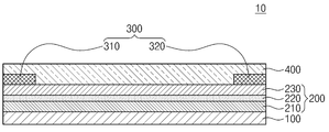
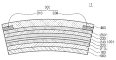
도 2는 도 1의 투명 면상 발열체를 나타낸 단면도이다.
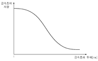
도 3a는 도 1의 금속 층의 두께에 따른 금속 층의 저항을 나타낸 그래프이다.
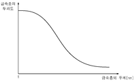
도 3b는 도 1의 금속 층의 두께에 따른 금속 층의 투과도를 나타낸 그래프이다.
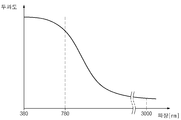
도 4는 도 1의 선택적 투과 층을 투사하는 광의 파장에 따른 투과도를 나타낸 그래프이다.
도 5은 본 발명의 일 실시예에 따른 투명 면상 발열체를 나타낸 단면도이다.
도 6은 도 1의 투명 면상 발열체가 구부러지는 모습을 나타낸 도면이다.
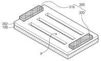
도 7은 본 발명의 일 실시예에 따른 투명 면상 발열체의 일부 구성을 나타낸 사시도이다.
도 8은 도 7의 투명 면상 발열체의 일부 구성을 나타낸 평면도이다.
200, 201, 202: 투명 발열 층 210: 결정핵 기반층
220: 금속 층 230: 선택적 투과 층
240: 방열 층 250: 도전성 산화물 층
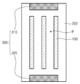
300: 전극 310: 제1 전극
320: 제2 전극 400: 투명 보호 층
500: 응력 완화 층
Claims (12)
- 투명 기판;
상기 투명 기판 상의 투명 발열 층; 및
상기 투명 발열 층 상에 배치되어, 상기 투명 발열 층과 전기적으로 연결되는 전극을 포함하고,
상기 투명 발열 층은:
상기 투명 기판 상에 배치되고, 상기 전극으로부터 외부 전원을 공급받아 발열하는 금속 층; 및
상기 투명 기판 상에 배치되고, 광의 적외선 영역 중 적어도 일부의 파장 영역을 차단하고, 상기 광의 일부 파장 영역을 투과하는 선택적 투과 층을 포함하는 투명 면상 발열체. - 제1항에 있어서,
상기 금속 층은 금(Au), 백금(Pt), 은(Ag), 알루미늄(Al), 구리(Cu), 아연(Zn), TiN, TaN, 텅스텐(W), 티타늄(Ti), 몰리브덴(Mo) 및 크롬(Cr) 중 적어도 어느 하나를 포함하는 투명 면상 발열체. - 제1항에 있어서,
상기 선택적 투과 층은 가시 광선 영역 중 적어도 일부의 파장 영역을 투과하는 투명 면상 발열체. - 제1항에 있어서,
상기 선택적 투과 층은 산화인튬주석(Indium Tin Oxide, ITO), 알루미늄이 도핑된 산화아연(ZnO:Al), 갈륨이 도핑된 산화아연(ZnO:Ga), 붕소가 도핑된 산화아연(ZnO:B), 플로오르가 도핑된 이산화주석(SnO₂:F), 이산화산화주석(SnO2), InZnO, 금(Au), 백금(Pt), 은(Ag), 알루미늄(Al), 몰리브덴(Mo) 및 크롬(Cr) 중 적어도 어느 하나를 포함하는 투명 면상 발열체. - 제1항에 있어서,
상기 투명 발열 층은 상기 금속 층 상에 배치되고, 상기 금속 층에서 발생된 열을 균일하게 방열하는 방열 층을 더 포함하는 투명 면상 발열체. - 제5항에 있어서,
상기 방열 층은 금(Au), 백금(Pt), 은(Ag), 알루미늄(Al), 구리(Cu), 아연(Zn), 니켈(Ni), TiN, TaN, 텅스텐(W), 티타늄(Ti), 몰리브덴(Mo) 및 크롬(Cr) 중 적어도 어느 하나를 포함하는 투명 면상 발열체. - 제1항에 있어서,
상기 투명 발열 층은 10 nm 내지 200 nm의 두께를 갖는 투명 면상 발열체. - 제1항에 있어서,
상기 투명 발열 층은 상기 투명 기판과 상기 금속 층 사이에 배치되는 결정핵 기반층(seed layer)을 더 포함하는 투명 면상 발열체. - 제8항에 있어서,
상기 투명 발열 층은 상기 금속 층과 전극 사이에 배치되는 도전성 산화물 층을 더 포함하고,
상기 금속 층은 상기 결정핵 기반층과 상기 도전성 산화물 층 사이에 배치되는 투명 면상 발열체. - 제1항에 있어서,
상기 투명 발열 층 상에 배치되어, 상기 전극을 덮는 투명 보호 층을 더 포함하는 투명 면상 발열체. - 제1항에 있어서,
상기 투명 기판의 하측에 배치되어, 상기 투명 기판에 가해지는 응력을 완화하는 응력 완화 층을 더 포함하는 투명 면상 발열체. - 제1항에 있어서,
상기 투명 발열 층은 상기 투명 기판의 일부가 노출되는 패턴을 갖는 투명 면상 발열체.
Priority Applications (1)
| Application Number | Priority Date | Filing Date | Title |
|---|---|---|---|
| US15/047,695 US20160249413A1 (en) | 2015-02-23 | 2016-02-19 | Transparent planar heater |
Applications Claiming Priority (2)
| Application Number | Priority Date | Filing Date | Title |
|---|---|---|---|
| KR20150025288 | 2015-02-23 | ||
| KR1020150025288 | 2015-02-23 |
Publications (2)
| Publication Number | Publication Date |
|---|---|
| KR20160103499A true KR20160103499A (ko) | 2016-09-01 |
| KR102012653B1 KR102012653B1 (ko) | 2019-08-22 |
Family
ID=56942653
Family Applications (1)
| Application Number | Title | Priority Date | Filing Date |
|---|---|---|---|
| KR1020150178462A Active KR102012653B1 (ko) | 2015-02-23 | 2015-12-14 | 투명 면상 발열체 |
Country Status (1)
| Country | Link |
|---|---|
| KR (1) | KR102012653B1 (ko) |
Cited By (3)
| Publication number | Priority date | Publication date | Assignee | Title |
|---|---|---|---|---|
| WO2021020914A1 (ko) * | 2019-07-31 | 2021-02-04 | 주식회사 아이테드 | 투명 발열 필름 |
| KR102228662B1 (ko) * | 2019-10-16 | 2021-03-16 | (주)아이테드 | 투명 발열 필름 |
| WO2025211683A1 (ko) * | 2024-04-01 | 2025-10-09 | 가천대학교 산학협력단 | 투명 발열체 및 그 제조방법 |
Citations (3)
| Publication number | Priority date | Publication date | Assignee | Title |
|---|---|---|---|---|
| JPH06338381A (ja) * | 1993-04-02 | 1994-12-06 | Mitsui Toatsu Chem Inc | 透明面状ヒーター及びその製造方法 |
| KR20080029230A (ko) * | 2006-09-28 | 2008-04-03 | 한국전자통신연구원 | 선택적 광차단층을 포함하는 염료감응 태양전지 |
| KR20130131922A (ko) * | 2012-05-25 | 2013-12-04 | 한국생산기술연구원 | 발열 효율 및 발열 균일도가 우수한 투명 면상 발열체의 제조방법 |
-
2015
- 2015-12-14 KR KR1020150178462A patent/KR102012653B1/ko active Active
Patent Citations (3)
| Publication number | Priority date | Publication date | Assignee | Title |
|---|---|---|---|---|
| JPH06338381A (ja) * | 1993-04-02 | 1994-12-06 | Mitsui Toatsu Chem Inc | 透明面状ヒーター及びその製造方法 |
| KR20080029230A (ko) * | 2006-09-28 | 2008-04-03 | 한국전자통신연구원 | 선택적 광차단층을 포함하는 염료감응 태양전지 |
| KR20130131922A (ko) * | 2012-05-25 | 2013-12-04 | 한국생산기술연구원 | 발열 효율 및 발열 균일도가 우수한 투명 면상 발열체의 제조방법 |
Cited By (3)
| Publication number | Priority date | Publication date | Assignee | Title |
|---|---|---|---|---|
| WO2021020914A1 (ko) * | 2019-07-31 | 2021-02-04 | 주식회사 아이테드 | 투명 발열 필름 |
| KR102228662B1 (ko) * | 2019-10-16 | 2021-03-16 | (주)아이테드 | 투명 발열 필름 |
| WO2025211683A1 (ko) * | 2024-04-01 | 2025-10-09 | 가천대학교 산학협력단 | 투명 발열체 및 그 제조방법 |
Also Published As
| Publication number | Publication date |
|---|---|
| KR102012653B1 (ko) | 2019-08-22 |
Similar Documents
| Publication | Publication Date | Title |
|---|---|---|
| US20160249413A1 (en) | Transparent planar heater | |
| KR101360786B1 (ko) | 발열 효율 및 발열 균일도가 우수한 투명 면상 발열체의 제조방법 | |
| KR20160103499A (ko) | 투명 면상 발열체 | |
| CN104698716B (zh) | 一种自适应电致变色智能窗 | |
| US9423295B2 (en) | Photo-sensor with a transparent substrate and an in-plane electrode pair | |
| CN105392591B (zh) | 用于获得提供有涂层的基材的方法 | |
| BR112014029496B1 (pt) | Janela com revestimento de uv-tratada e baixa-e e método para fazer o mesmo | |
| SA109300073B1 (ar) | إلكترود أمامي للاستخدام في جهاز ڤٌلطائي ضوئي وطريقة لتصنيعه | |
| EP2327543A1 (en) | Panel including thermochromic layer and electric conductive layer | |
| EP3096345B1 (en) | Infrared emitter | |
| JP7697568B2 (ja) | センサ用カバー、及びセンサモジュール | |
| KR20140116119A (ko) | 복사 방출 유기 소자 | |
| KR101465518B1 (ko) | 무반사 기능을 갖는 투명 면상 발열체 | |
| EP3004980A1 (en) | An electrophoretic solar control device | |
| KR20130131920A (ko) | 투명 면상 발열체 및 이의 제조방법 | |
| KR101602922B1 (ko) | 투명 컬러 태양전지 | |
| JP2007150157A (ja) | 薄膜トランジスタ | |
| CN111394693B (zh) | 掩膜板和其制备方法及使用该掩膜板制备光伏组件的方法 | |
| US11710628B2 (en) | Infrared light radiation device | |
| JP2004311845A (ja) | 発電機能を有する可視光透過構造体 | |
| US20170324005A1 (en) | Optoelectronic semiconductor chip | |
| RU2020126578A (ru) | Прозрачное проводящее покрытие для емкостной сенсорной панели и способ ее изготовления | |
| KR20200040447A (ko) | 광 선택 투과형 윈도우 | |
| JP2024033210A (ja) | 深紫外線発光装置 | |
| WO2019208252A1 (ja) | 赤外線放射装置 |
Legal Events
| Date | Code | Title | Description |
|---|---|---|---|
| PA0109 | Patent application |
Patent event code: PA01091R01D Comment text: Patent Application Patent event date: 20151214 |
|
| PG1501 | Laying open of application | ||
| A201 | Request for examination | ||
| PA0201 | Request for examination |
Patent event code: PA02012R01D Patent event date: 20170802 Comment text: Request for Examination of Application Patent event code: PA02011R01I Patent event date: 20151214 Comment text: Patent Application |
|
| E902 | Notification of reason for refusal | ||
| PE0902 | Notice of grounds for rejection |
Comment text: Notification of reason for refusal Patent event date: 20181127 Patent event code: PE09021S01D |
|
| E701 | Decision to grant or registration of patent right | ||
| PE0701 | Decision of registration |
Patent event code: PE07011S01D Comment text: Decision to Grant Registration Patent event date: 20190520 |
|
| GRNT | Written decision to grant | ||
| PR0701 | Registration of establishment |
Comment text: Registration of Establishment Patent event date: 20190814 Patent event code: PR07011E01D |
|
| PR1002 | Payment of registration fee |
Payment date: 20190816 End annual number: 3 Start annual number: 1 |
|
| PG1601 | Publication of registration | ||
| PR1001 | Payment of annual fee |
Payment date: 20220720 Start annual number: 4 End annual number: 4 |
|
| PR1001 | Payment of annual fee |
Payment date: 20240724 Start annual number: 6 End annual number: 6 |