KR20160083888A - Hall sensor readout system with offset determination using the Hall element itself - Google Patents
Hall sensor readout system with offset determination using the Hall element itself Download PDFInfo
- Publication number
- KR20160083888A KR20160083888A KR1020167014458A KR20167014458A KR20160083888A KR 20160083888 A KR20160083888 A KR 20160083888A KR 1020167014458 A KR1020167014458 A KR 1020167014458A KR 20167014458 A KR20167014458 A KR 20167014458A KR 20160083888 A KR20160083888 A KR 20160083888A
- Authority
- KR
- South Korea
- Prior art keywords
- offset
- read signal
- hall
- magnetic field
- hall element
- Prior art date
Links
Images


Classifications
-
- G—PHYSICS
- G01—MEASURING; TESTING
- G01R—MEASURING ELECTRIC VARIABLES; MEASURING MAGNETIC VARIABLES
- G01R33/00—Arrangements or instruments for measuring magnetic variables
- G01R33/0023—Electronic aspects, e.g. circuits for stimulation, evaluation, control; Treating the measured signals; calibration
- G01R33/0035—Calibration of single magnetic sensors, e.g. integrated calibration
-
- G—PHYSICS
- G01—MEASURING; TESTING
- G01R—MEASURING ELECTRIC VARIABLES; MEASURING MAGNETIC VARIABLES
- G01R15/00—Details of measuring arrangements of the types provided for in groups G01R17/00 - G01R29/00, G01R33/00 - G01R33/26 or G01R35/00
- G01R15/14—Adaptations providing voltage or current isolation, e.g. for high-voltage or high-current networks
- G01R15/20—Adaptations providing voltage or current isolation, e.g. for high-voltage or high-current networks using galvano-magnetic devices, e.g. Hall-effect devices, i.e. measuring a magnetic field via the interaction between a current and a magnetic field, e.g. magneto resistive or Hall effect devices
- G01R15/202—Adaptations providing voltage or current isolation, e.g. for high-voltage or high-current networks using galvano-magnetic devices, e.g. Hall-effect devices, i.e. measuring a magnetic field via the interaction between a current and a magnetic field, e.g. magneto resistive or Hall effect devices using Hall-effect devices
-
- G—PHYSICS
- G01—MEASURING; TESTING
- G01R—MEASURING ELECTRIC VARIABLES; MEASURING MAGNETIC VARIABLES
- G01R33/00—Arrangements or instruments for measuring magnetic variables
- G01R33/0017—Means for compensating offset magnetic fields or the magnetic flux to be measured; Means for generating calibration magnetic fields
-
- G—PHYSICS
- G01—MEASURING; TESTING
- G01R—MEASURING ELECTRIC VARIABLES; MEASURING MAGNETIC VARIABLES
- G01R33/00—Arrangements or instruments for measuring magnetic variables
- G01R33/0023—Electronic aspects, e.g. circuits for stimulation, evaluation, control; Treating the measured signals; calibration
- G01R33/0029—Treating the measured signals, e.g. removing offset or noise
-
- G—PHYSICS
- G01—MEASURING; TESTING
- G01R—MEASURING ELECTRIC VARIABLES; MEASURING MAGNETIC VARIABLES
- G01R33/00—Arrangements or instruments for measuring magnetic variables
- G01R33/007—Environmental aspects, e.g. temperature variations, radiation, stray fields
- G01R33/0082—Compensation, e.g. compensating for temperature changes
-
- G—PHYSICS
- G01—MEASURING; TESTING
- G01R—MEASURING ELECTRIC VARIABLES; MEASURING MAGNETIC VARIABLES
- G01R33/00—Arrangements or instruments for measuring magnetic variables
- G01R33/02—Measuring direction or magnitude of magnetic fields or magnetic flux
- G01R33/06—Measuring direction or magnitude of magnetic fields or magnetic flux using galvano-magnetic devices
- G01R33/07—Hall effect devices
- G01R33/072—Constructional adaptation of the sensor to specific applications
- G01R33/075—Hall devices configured for spinning current measurements
Abstract
도핑된 반도체 물질로 제조된 플레이트-형상 센서 요소를 가진 적어도 하나의 홀 요소(101)를 포함하는 홀 센서(100)의 오프셋 보상을 제공하는 방법은, 홀 요소 자체에 대한 측정을 이용하는 단계를 포함한다. 상기 방법은 자기장에 실질적으로 의존하는 적어도 하나의 홀 요소로부터의 제 1 판독 신호(VH)를 획득하는 단계와, 자기장에 실질적으로 독립적인 적어도 하나의 홀 요소로부터의 제 2 판독 신호(VP)를 획득하는 단계와, 상기 제 1 판독 신호(VH)에 대한 오프셋(Vo)의 예측치(![]()
![]()
Description
본 발명은 홀 센서 판독치의 오프셋 결정 방법 및 장치에 관한 것으로서, 상기 오프셋은 온도, 온도 구배, (패키지-유도) 기계적 응력, 도핑 농도의 불균질성, 및 기하학적 오차에 기인한다. 특히, 본 발명은 홀 플레이트 자체에 대한 측정치를 이용함으로써, 홀 플레이트를 포함하는 센서의 오프셋 보상 방법 및 장치에 관련된다. The present invention relates to a method and apparatus for determining offset of a Hall sensor readout, said offset being due to temperature, temperature gradient, (package-induced) mechanical stress, heterogeneity of doping concentration, and geometric error. In particular, the present invention relates to a method and apparatus for offset compensation of a sensor comprising a hole plate, by using measurements on the hole plate itself.
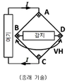
홀 요소는 자기장의 기결정된 성분에 비례하는 전기 출력 신호를 제공하도록 홀 효과에 기초한 자기장 센서다. 기본 홀 소자는 적어도 4개의 전기 접촉부를 구비한 전도 물질로 구성된다. 홀 효과를 이용하기 위해, 소자를 통해 전류가 흘러야 한다. 기본 전류 I는 접촉부 중 2개를 통해 공급되고, 이는 전류 접촉부로 불릴 것이다. 감지 접촉부라고 불리는 2개의 다른 접촉부는 등전위선 상에 통상적으로 배치되어, 자기장 부재시 감지 접촉부 사이의 전압차를 0으로 만든다. 수평 홀 요소를 이용한 자기장 성분 Bz 측정 원리가 도 1에 도시된다. 홀 판독을 위해, 전류 접촉부 A, C 및 감지 접촉부 B, D가 서로 교번된다. 전류 I가 전류 접촉부 A, C에 인가되고 평면-외 자기장 Bz가 소자에 인가되면, 인가된 자기장 Bz에 비례하는 홀 전압 VH가 감지 접촉부 B, D 사이에 나타날 것이다; 다시 말해서, VH = VB-VD.The Hall element is a magnetic field sensor based on Hall effect to provide an electrical output signal proportional to a predetermined component of the magnetic field. The basic Hall element is composed of conductive material with at least four electrical contacts. To utilize the Hall effect, current must flow through the device. The basic current I is supplied through two of the contacts, which will be referred to as the current contacts. Two other contacts, commonly referred to as sensing contacts, are typically placed on the equipotential lines to zero the voltage difference between sensing contacts in the absence of a magnetic field. The principle of measuring the magnetic field component Bz using a horizontal Hall element is shown in Fig. For hole reading, current contacts A, C and sense contacts B, D alternate with each other. When a current I is applied to current contacts A, C and an out-of-plane magnetic field Bz is applied to the device, a Hall voltage V H proportional to the applied magnetic field Bz will appear between sensing contacts B, D; In other words, V H = V B -V D.
홀 센서는 홀 요소 또는 홀 요소들의 클러스터와, 홀 요소를 작동시키기 위한, 그리고 홀 요소의 출력 신호를 평가하기 위한, 전자 회로를 포함한다. 홀 센서는 반도체 칩에 내장된 집적 회로로 제조된다. 반도체 칩이 하우징에 패키징된다. 홀 요소는 프로세스-관련 및 기하구조-관련 변화로부터 발생하는 오프셋을 가진다. 오프셋은 복수의 홀 요소들을 병렬로 (클러스터) 연결함으로써, 및/또는 알려진 스피닝 전류 방법을 이용하여 작동함으로써, 효과적으로 최소화될 수 있다. 이는 수많은 특허 문서, 예를 들어, WO 0118556, EP 548391, 및 DE 4302342를 통해 알려져 있다. The Hall sensor includes a cluster of Hall elements or Hall elements, and electronic circuits for operating the Hall elements and for evaluating the output signals of the Hall elements. The Hall sensor is manufactured as an integrated circuit embedded in a semiconductor chip. The semiconductor chip is packaged in the housing. The Hall element has an offset resulting from process-related and geometry-related changes. Offset can be minimized effectively by connecting a plurality of Hall elements in parallel (cluster), and / or by operating using a known spinning current method. This is known from numerous patent documents, for example, WO 0118556, EP 548391, and DE 4302342.
홀 요소는 가령, CMOS 기술로, 반도성 소자에 쉽게 집적될 수 있고, 이는 고급 온-칩 판독 회로와 조합될 수 있음을 의미한다. 다른 (가령, 판독) 소자와 함께 집적되는 홀 소자의 영향은, 홀 요소가 기판 및 기타 구성요소로부터 전기적으로 분리될 필요가 있다는 점이다. 집적 기술에서, 이는 리버스-바이어스 PN 정션을 이용함으로써 실현될 수 있다. The Hall element can, for example, be easily integrated into a semiconductive element with CMOS technology, which means that it can be combined with advanced on-chip readout circuitry. The effect of Hall elements integrated with other (e.g., read) elements is that the Hall elements need to be electrically isolated from the substrate and other components. In an integration technique, this can be realized by using a reverse-bias PN junction.
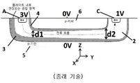
도 2에서, 여기가 이루어지는 선(도 1의 접촉부 A 및 C를 통하는 선)을 따라 잘려진, 일체형 수평 홀 플레이트의 단면이 도시된다. 예를 들자면, p-형 기판을 이용한 CMOS 프로세스가 도시되어 있다. 그 후 실제 홀 플레이트는 n-웰의 n-형 물질로 구성된다. 본 예에서, p-형 커버층(상부 실드(shield))가 상부에 도시되며, 이는 다양한 이유들 중 하나 이상을 위해 종종 제공된다(차폐 개선, 소자 노이즈 감소, 등). 도 2에서, 기판 및 상부 실드 모두 접지부(0V)에 연결된다. 홀 판독 중, 전류 I가 플레이트를 통해 흘러야 한다. 이를 위해, 노드 A 및 노드 C는 서로 다른 전압에 놓여야 한다. 예를 들자면, 인가 바이어스 방법이 노드 A에서 3.0V, 노드 C에서 1.0V로 여기서 가정된다. PN-정션 이론으로부터 잘 알려져 있듯이, p-형 물질과 n-형 물질 간의 임의의 전이에서 공핍 영역이 형성된다. PN-정션이 항상 리버스-바이어스되도록 바이어스가 이루어진다. 리버스-바이어스 전이는 플레이트를 전기적으로 분리시킨다. 분리된 공핍 영역은 홀 플레이트 내로 p-형 기판 및 p-형 커버 근처로 연장되고(도 2의 그레이 영역), 적은 개수의 자유 전하 운반자를 가진다(즉, 이 영역들이 거의 완벽한 아이솔레이터로 간주될 수 있다). 그 결과, 홀 플레이트의 유효 두께가 감소한다. 공핍 구역의 실제 크기는 PN-정션에 걸쳐 로컬 (리버스) 전압과 비-선형으로 변화한다. 이러한 리버스-전압은 플레이트에 걸쳐 변화하고, 전류가 들어오는 노드에서 최대이고(고전위에서 노드 A), 전류가 나가는 노드에서 최소다(저전위에서 노드 C). 그 결과, 고전압측에서의 플레이트 두께(도 2의 d1)가 저전압측에서의 플레이트 두께(도 2의 d2)보다 작고, 이는 A로부터 C 방향으로 플레이트 두께의 불균일성을 의미한다. 다시 말해서, 홀 플레이트의 두께가 일정하지 않고, 플레이트에 걸쳐 변화한다. 불행하게도, 전류 바이어싱을 이용할 때, (노드 A와 C 사이에서) 효과적으로 인가되는 전압은 온도에 크게 의존할 뿐 아니라, 압전 응력-효과 및 심지어 홀 효과 자체도 전압에 영향을 미친다(즉, 전압이 도 2의 X-방향으로도 변화한다). 이 효과들이 플레이트의 두께를 변화시키기 때문에, 자기 센서의 감도 및 선형성에 영향을 미친다. In Fig. 2, a section of an integral horizontal hole plate is shown cut along a line through which the excitation is made (line through contacts A and C of Fig. 1). For example, a CMOS process using a p-type substrate is shown. The actual hole plate is then made of the n-type material of the n-well. In this example, a p-type cover layer (upper shield) is shown at the top, which is often provided for more than one of a variety of reasons (shielding improvement, device noise reduction, etc.). In Fig. 2, both the substrate and the upper shield are connected to ground (0V). During the hole reading, the current I must flow through the plate. To this end, node A and node C must be at different voltages. For example, it is assumed here that the applied bias method is 3.0V at node A and 1.0V at node C. As is well known from the PN junction theory, a depletion region is formed at any transition between a p-type material and an n-type material. Bias is applied so that the PN-junction is always reverse-biased. The reverse-bias transition electrically isolates the plate. The isolated depletion region extends into the hole plate near the p-type substrate and the p-type cover (gray region in Figure 2) and has a small number of free charge carriers (i. E., These regions can be regarded as almost perfect isolators have). As a result, the effective thickness of the hole plate is reduced. The actual size of the depletion region varies non-linearly with the local (reverse) voltage across the PN junction. This reverse-voltage varies across the plate, the current is at the maximum at the incoming node (node A at high), and minimum at the outgoing current (node C at low). As a result, the plate thickness (d1 in Fig. 2) on the high voltage side is smaller than the plate thickness (d2 in Fig. 2) on the low voltage side, which means the plate thickness nonuniformity in the A to C direction. In other words, the thickness of the hole plate is not constant but varies across the plate. Unfortunately, when using current biasing, the voltage effectively applied (between nodes A and C) is not only highly dependent on temperature, but also the piezoelectric stress-effect, and even the Hall effect itself, also affects the voltage Direction also changes in the X-direction in Fig. 2). Since these effects vary the thickness of the plate, it affects the sensitivity and linearity of the magnetic sensor.
홀 센서의 중요한 특성은 (자기) 감도다. 이상적인 경우에, 감도는 일정 값이고, 측정되는 홀 전압은 온도, 응력, 등에 독립적인, 자기장 강도의 선형 함수다. 그러나 실제로는, 이것이 완전한 사실이 아니다. 하지만, (예를 들어, 홀-기반 선형 전류 센서에서와 같은) 많은 응용예에서, 감도의 절대 정확도가 중요하다. 이는 온도, 응력, 등과 같은 환경적 조건과의 교차-감도가 감소해야만 하고, 또는, 적어도 이를 보상할 가능성이 있어야 함을 의미한다. 추가적으로, 홀 전압에 대한 감도의 종속성 - 홀 전압은 인가 자기장에 의존 - 은, 센서 특성이 자기장의 비선형 함수가 됨을 의미한다. An important characteristic of hall sensors is (magnetic) sensitivity. In an ideal case, the sensitivity is a constant value, and the Hall voltage measured is a linear function of the magnetic field strength, independent of temperature, stress, and so on. But in reality, this is not a complete fact. However, in many applications (such as, for example, in Hall-based linear current sensors), absolute accuracy of sensitivity is important. This means that the cross-sensitivity to environmental conditions such as temperature, stress, etc. must either decrease or at least have to be able to compensate for it. Additionally, the dependence of sensitivity on the Hall voltage - the Hall voltage depends on the applied magnetic field - means that the sensor characteristic is a nonlinear function of the magnetic field.
하우징에 패키징된 홀 요소를 포함하는 반도체 칩은 온도 및 습도와 같은 환경적 영향에 좌우되는 기계적 응력을 받는다. 기계적 응력 변화는 홀 요소의 오프셋 변화를 야기하고, 압전-홀 효과로 인해 홀 요소들의 감도 변화 역시 야기한다. 감도 변화를 보상하기 위해, 기계적 응력을 검출하는 응력 센서를 이용하고, 압전-홀 효과에 의해 야기되는 홀 요소 감도 변화를 보상하기 위해 그 출력 신호를 이용하는 것이 예를 들어, DE 10154495, DE 10154498, DE 102004003853, DE 102008051949 호로부터 알려져 있다. Semiconductor chips, including Hall elements packaged in a housing, are subject to mechanical stresses that are dependent on environmental influences such as temperature and humidity. The mechanical stress changes cause an offset change in the Hall element, and also cause a change in the sensitivity of the Hall elements due to the piezoelectric-Hall effect. To compensate for the sensitivity change, it is known to use a stress sensor that detects mechanical stresses and to use the output signal to compensate for Hall element sensitivity variations caused by the piezoelectric-hole effect, for example in DE 10154495, DE 10154498, DE 102004003853, DE 102008051949.
홀 요소의 오프셋을 결정하고, 선택적으로, 보상하기 위한 실용적 방법 및 디바이스를 제공하는 것이 본 발명의 실시예의 목적이다. It is an object of embodiments of the present invention to provide a practical method and device for determining and optionally compensating for the offset of the Hall element.
이 목적은 본 발명의 실시예에 따른 방법 및 디바이스에 의해 실현된다. This object is achieved by a method and a device according to embodiments of the present invention.
일 형태에서, 본 발명은 도핑된 반도체 물질로 제조된 플레이트-형상 센서 요소를 가진 적어도 하나의 홀 요소를 포함하는 홀 센서에서의 오프셋 결정 방법을 제공하며, 상기 방법은 홀 요소 자체에 대한 측정을 이용한다. 이 방법은 자기장에 실질적으로 의존하는 적어도 하나의 홀 요소로부터의 제 1 판독 신호를 획득하는 단계와, 자기장에 실질적으로 독립적인 적어도 하나의 홀 요소로부터의 제 2 판독 신호를 획득하는 단계와, 제 1 판독 신호에 대한 오프셋의 예측치를 얻기 위해 제 2 판독 신호를 이용하는 단계를 포함한다. 따라서, 그 후 오프셋의 획득된 예측치는, 후속하여, 제 1 판독 신호로부터 오프셋 예측치를 제거함으로써, 제 1 판독 신호에 대한 오프셋 보상을 제공하는데 사용될 수 있다. In one aspect, the present invention provides a method of determining an offset in an Hall sensor comprising at least one Hall element having a plate-shaped sensor element made of a doped semiconductor material, the method comprising: . The method includes obtaining a first read signal from at least one Hall element that is substantially dependent on a magnetic field, obtaining a second read signal from at least one Hall element substantially independent of the magnetic field, And using a second read signal to obtain a prediction of an offset for one read signal. Thus, the obtained predicted value of the offset thereafter can subsequently be used to provide offset compensation for the first read signal by removing the offset prediction from the first read signal.
본 발명의 범주에서 "자기장에 실질적으로 의존하는"은, 자기장이 측정 결과에 대해 영향을 가짐을 의미한다. 본 발명의 범주에서 "자기장에 실질적으로 독립적인"은 자기장이 측정 결과에 영향이 없음을 의미한다. 후자는 알려지지 않은 자기장이 존재할 수 있으나 제 2 판독 신호 획득을 위한 측정 중, 존재할 필요는 없다는 것을 암시한다. In the context of the present invention, "substantially dependent on the magnetic field" means that the magnetic field has an influence on the measurement result. &Quot; Substantially independent of the magnetic field "in the context of the present invention means that the magnetic field has no effect on the measurement result. The latter implies that an unknown magnetic field may be present, but it does not have to be present during the measurements for acquiring the second read signal.
다른 형태에서, 본 발명은 오프셋 보상 기능을 가진 홀 센서를 제공한다. 홀 센서는 적어도 하나의 홀 요소 - 각각의 홀 요소는 도핑된 반도체 물질로 제조된 플레이트-형상 센서 요소를 가짐 - 와, 자기장에 실질적으로 의존하는(자기장이 측정 결과에 영향을 미침) 적어도 하나의 홀 요소로부터 제 1 판독 신호를 획득하기 위한 센서 수단과, 자기장에 실질적으로 독립적인(자기장이 측정 결과에 영향을 미치지 않음) 적어도 하나의 홀 요소로부터 제 2 판독 신호를 획득하기 위한 센서 수단과, 적어도 하나의 홀 요소 자체에 대한 측정으로부터 획득되는 제 2 판독 신호를 이용함으로써 제 1 판독 신호에 대한 오프셋을 보상하기 위한 수단을 포함한다. 본 발명의 실시예에서, 오프셋 보상 수단은 대응하는 아날로그 신호 처리에 의해 아날로그 방식으로 구현될 수 있다. 본 발명의 대안의 실시예에서, 오프셋 보상 수단은, 적절히 프로그래밍된 컴퓨팅 수단을 이용함으로써 디지털 방식으로 구현될 수 있다. 다른 대안의 실시예에서, 조합된 아날로그-디지털 구현이 가능하다. In another aspect, the present invention provides a Hall sensor having an offset compensation function. The Hall sensor has at least one Hall element, each Hall element having a plate-shaped sensor element made of a doped semiconductor material, and at least one Sensor means for acquiring a second read signal from at least one hall element substantially independent of the magnetic field (the magnetic field does not affect the measurement result) And means for compensating for an offset for the first read signal by using a second read signal obtained from measurements on at least one of the hole elements themselves. In an embodiment of the present invention, the offset compensation means can be implemented in an analog manner by corresponding analog signal processing. In an alternative embodiment of the present invention, the offset compensation means can be implemented in a digital manner by using appropriately programmed computing means. In another alternative embodiment, a combined analog-digital implementation is possible.
또 다른 형태에서, 본 발명은 적어도 하나의 홀 요소를 포함하는 홀 센서와 함께 이용하기 위한 컨트롤러를 제공한다. 컨트롤러는 자기장에 실질적으로 의존하는(자기장이 측정 결과에 영향을 미침) 적어도 하나의 홀 요소로부터 제 1 판독 신호를 획득하도록 구성되고, 자기장에 실질적으로 독립적인(자기장이 측정 결과에 영향을 미치지 않음) 적어도 하나의 홀 요소로부터 제 2 판독 신호를 획득하도록 구성되며, 제 1 판독 신호에 대한 오프셋의 예측치를 획득하기 위해 제 2 판독 신호를 이용하도록 구성된다. In another aspect, the invention provides a controller for use with a Hall sensor comprising at least one Hall element. The controller is configured to obtain a first read signal from at least one Hall element that is substantially dependent on the magnetic field (the magnetic field affects the measurement result) and is substantially independent of the magnetic field (the magnetic field does not affect the measurement result ) Configured to obtain a second read signal from at least one of the Hall elements and to use a second read signal to obtain a prediction of the offset for the first read signal.
본 발명은 홀 센서와 관련된 컴퓨팅 디바이스 상에서 실행될 때, 본 발명의 실시예에 따른 방법의 기능을 제공하는 컴퓨터 프로그램 프로덕트를 또한 포함한다. 이러한 컴퓨터 프로그램 프로덕트는 프로그래머블 프로세서에 의한 실행을 위해 기계-판독가능 코드를 지닌 캐리어 매체에 유형으로 포함될 수 있다. 따라서 본 발명은 컴퓨팅 수단 상에서 실행될 때, 앞서 설명된 방법을 실행하기 위한 명령어를 제공하는 컴퓨터 프로그램 프로덕트를 지닌 캐리어 매체에 관련된다. "캐리어 매체"라는 용어는 실행을 위한 명령어를 프로세서에 제공함에 참가하는 임의의 매체를 의미한다. 이러한 매체는 비휘발성 매체 및 전송 매체를 포함하는, 그러나 이에 제한되지 않는, 많은 형태를 취할 수 있다. 비휘발성 매체는 예를 들어, 광학 디스크 또는 자기 디스크, 가령, 대용량 스토리지의 일부분인 저장 장치를 포함한다. The present invention also includes a computer program product that when executed on a computing device associated with a Hall sensor, provides a function of a method according to an embodiment of the present invention. Such a computer program product may be typed into a carrier medium having machine-readable code for execution by a programmable processor. Accordingly, the present invention relates to a carrier medium having a computer program product, when executed on a computing means, for providing instructions for carrying out the methods described above. The term "carrier medium" means any medium that participates in providing instructions to a processor for execution. Such media can take many forms, including, but not limited to, non-volatile media and transmission media. Non-volatile media include, for example, optical disks or magnetic disks, e.g., storage devices that are part of a mass storage.
발명의 특정 선호 형태는 첨부된 독립항 및 종속항에서 제시된다. 적절하다면, 그리고, 단지 청구항에 명시적으로 제시된 것만이 아니라, 종속항으로부터의 특징들이 독립항의 특징들과 조합될 수 있고, 다른 종속항의 특징들과도 조합될 수 있다. Certain preferred forms of the invention are set forth in the appended independent and dependent claims. Where appropriate, and not merely those explicitly set forth in the claims, features from a dependent claim may be combined with features of the independent claim, and may be combined with features of other dependent claims.
발명과, 선행 기술에 비추어 실현된 장점을 요약하기 위한 용도로, 발명의 소정의 목적 및 장점이 앞서 설명된 바 있다. 물론, 모든 이러한 목적 또는 장점이 발명의 특정 실시예에 따라 반드시 실현될 수 있는 것은 아니다. 따라서, 예를 들어, 발명이 여기서 설명 또는 암시되는 다른 목적 또는 장점을 반드시 실현할 필요없이, 여기서 설명되는 일 장점 또는 여러 장점들을 실현 또는 최적화시키는 방식으로 포함 또는 실시될 수 있음을 당 업자가 이해할 것이다. For purposes of summarizing the invention and the advantages realized in light of the prior art, certain objects and advantages of the invention have been described above. Of course, not all of these objects or advantages may be realized in accordance with the specific embodiments of the invention. Thus, it will be understood by those skilled in the art that the invention may be embodied or carried out in a manner that realizes or optimizes one or more of the advantages or advantages described herein without necessarily requiring other aspects or advantages herein described or implied herein .
발명의 위 형태 및 다른 형태들이 이후 설명되는 실시예를 참조하여 명백해질 것이다. The above and other aspects of the invention will be apparent from and elucidated with reference to the embodiments described hereinafter.
도 1은 자기장 성분의 강도를 나타내는 홀-전압을 측정하는 알려진 방식을 보여주며, 여기 소스가 2개의 접촉부에 인가되고, 출력이 2개의 다른 접촉부에 걸쳐 감지된다.
도 2는 대각선 AC를 따라, 도 1에 따른 일체형 수평 홀 플레이트의 단면도다. 정션-분리 홀 소자에서의 공핍층 변화는 불균일한 그리고 전압-의존적인 플레이트 두께 변화를 야기한다.
도 3은 본 발명의 실시예에 따른 홀 자기 센서의 유연한 구조를 도시한다.
도 4는 4개의 홀-형 측정치의 개관을 제시한다.
도 5는 자기 성분을 취소시키도록 상호연결된 홀-형 측정치를 갖는 2개의 홀 요소의 예를 도시한다. 도면의 상부는 2개의 홀 플레이트의 직렬-직렬 연결을 도시하고, 도면의 하부는 2개의 홀 플레이트의 병렬-병렬 연결을 도시한다.
도 6은 8개의 "반데포"(Van der Pauw)-형 측정치의 개관을 도시한다.
도 7은 2개의 "반데포"-형 측정치의 차이를 직접 측정할 수 있도록, 각각의 플레이트가 "반데포"-형 구조로 작동되는, 2개의 플레이트의 감지 노드들의 상호연결을 도시한다. 여기 노드는 병렬로 놓일 수 있다.
도 8은 2개의 "반데포"-형 측정치의 차이와 홀-형 측정의 오프셋 간의 관계를 도시한다. Figure 1 shows a known manner of measuring the Hall-voltage representing the intensity of a magnetic field component, wherein an excitation source is applied to two contacts and an output is sensed across two different contacts.
Figure 2 is a cross-sectional view of the integral horizontal hole plate according to Figure 1, along a diagonal AC; Depletion layer variation in the junction-separation Hall element causes non-uniform and voltage-dependent plate thickness variations.
FIG. 3 shows a flexible structure of a Hall-effect magnetic sensor according to an embodiment of the present invention.
Figure 4 presents an overview of four hole-type measurements.
Figure 5 shows an example of two hall elements with hole-type measurements interconnected to cancel magnetic components. The upper part of the figure shows a series-series connection of two hole plates and the lower part of the figure shows a parallel-parallel connection of two hole plates.
Figure 6 shows an overview of eight "Van der Pauw " -type measurements.
Figure 7 shows the interconnection of the sensing nodes of the two plates, in which each plate is operated in an " anti-deo "-type structure, so that the difference between the two" The nodes here can be placed in parallel.
Figure 8 shows the relationship between the difference of two "anti-demodulator" -type measurements and the offset of the hall-type measurement.
본 발명은 도면을 참조하여 특정 실시예와 관련하여 설명되지만, 발명은 이에 제한되지 않고 청구범위에 의해서만 제한된다. While the invention will be described with reference to specific embodiments with reference to the drawings, the invention is not limited thereto but only by the claims.
상세한 설명 및 청구범위에서 제 1, 제 2, 등의 용어는 유사한 요소들 간을 구분하기 위해 사용되며, 시간상, 공간상, 순위 형태로, 또는 그외 다른 방식으로, 꼭 순서를 설명하기 위해 사용되는 것이 아니다. 이와 같이 사용되는 용어들은 적절한 상황 하에 상호교환가능하고, 여기서 설명되는 발명의 실시예는 여기서 설명 또는 예시되는 다른 시퀀스로 작동할 수 있다. In the description and claims, the terms first, second, etc. are used to distinguish between similar elements and are used to describe the order by time, space, in the form of a rank, or otherwise It is not. The terms thus used are interchangeable under appropriate circumstances, and embodiments of the invention described herein may operate with other sequences as described or illustrated herein.
상세한 설명 및 청구범위에서 위, 아래, 등과 같은 용어는 설명 용도로 사용되며, 꼭 상대적 위치를 설명하는 것은 아니다. 이렇게 사용되는 용어는 적절한 상황 하에 상호교환가능하고, 여기서 설명되는 발명의 실시예는 여기서 설명 또는 예시되는 다른 배향으로 작동할 수 있다. In the description and the claims, terms such as up, down, and the like are used for descriptive purposes and not necessarily relative positions. The terms thus used are interchangeable under appropriate circumstances, and embodiments of the invention described herein may operate with other orientations as described or illustrated herein.
청구범위에서 사용되는 "포함하는"이라는 용어는 이후 나열되는 수단에 제한되는 것으로 해석되어서는 안되며, 다른 요소 또는 단계들을 배제하지 않는다. 따라서, 거명되는 특징, 정수, 단계, 또는 구성요소들의 존재를 명시할 뿐 아니라, 하나 이상의 다른 특징, 정수, 단계, 또는 구성요소들의 존재 또는 추가를 배제하지 않는다. 따라서, "수단 A 및 수단 B를 포함하는 디바이스"라는 표현의 범위는 구성요소 A 및 B 만으로 구성되는 디바이스로 제한되어서는 안된다. 본 발명과 관련하여, 디바이스의 관련 구성요소들만이 A 및 B임을 의미한다. As used in the claims, the term " comprising "should not be interpreted as being limited to the means listed thereafter, and does not exclude other elements or steps. Accordingly, the specification does not exclude the presence of stated features, integers, steps, or components, but does not preclude the presence or addition of one or more other features, integers, steps, or components. Therefore, the scope of the expression "a device including the means A and the device B" should not be limited to a device composed of only the elements A and B. In the context of the present invention, it is meant that only the relevant components of the device are A and B.
본 명세서 전체를 통해, "일 실시예" 또는 "하나의 실시예"는 실시예와 연계하여 설명되는 특정 특징, 구조, 또는 특성이 본 발명의 적어도 하나의 실시예에 포함됨을 의미한다. 따라서, 본 명세서 전체 내 다양한 부분에서 "하나의 실시예에서" 또는 "일 실시예에서"라는 표현의 등장은 모두 동일한 실시예를 언급하는 것이 아니지만, 그럴 수도 있다. 더욱이, 특정 특징, 구조, 또는 특성이, 하나 이상의 실시예에서, 당 업자에게 명백하다면, 임의의 적절한 방식으로 조합될 수 있다. Throughout this specification, "an embodiment" or "an embodiment" means that a particular feature, structure, or characteristic described in connection with the embodiment is included in at least one embodiment of the invention. Thus, the appearances of the phrase "in one embodiment " or" in one embodiment "in various portions throughout this specification are not necessarily all referring to the same embodiment, but may be so. Furthermore, certain features, structures, or characteristics may be combined in any suitable manner, provided that they are, in one or more embodiments, obvious to the skilled artisan.
마찬가지로, 발명의 예시적 실시예의 설명에서, 다양한 신규적 형태들 중 하나 이상의 이해를 돕기 위해 그리고 발명을 나열하기 위한 용도로, 발명의 다양한 특징들이 단일 실시예, 도면, 또는 설명에서 함께 그룹화될 수 있다. 그러나, 이러한 개시 방법은 청구되는 발명이 각각의 청구항에서 명시적으로 언급되는 것보다 많은 특징들을 요한다는 의도를 반영하는 것으로 이해되어서는 안된다. 대신, 다음의 청구항이 반영하듯이, 신규적 형태는 선행하는 단일 개시 실시예의 모든 특징들보다 적은 특징들에 있다. 따라서, 상세한 설명에 이어지는 청구범위는 이러한 상세한 설명에 명시적으로 포함되며, 각각의 청구항은 본 발명의 별도의 실시예로 자체적으로 성립된다. Likewise, in the description of exemplary embodiments of the invention, various features of the invention may be grouped together in a single embodiment, drawing, or description, for purposes of understanding one or more of the various novel aspects, have. However, this disclosure should not be interpreted as reflecting an intention that the claimed invention requires more features than are expressly recited in each claim. Instead, as the following claims reflect, the novelty lies in less features than all features of the preceding single disclosure embodiment. Accordingly, the claims following the detailed description are expressly included in this detailed description, with each claim standing on its own as a separate embodiment of the present invention.
더욱이, 여기서 설명되는 일부 실시예가 다른 실시예에 포함된 일부 특징들을 포함하면서 일부 다른 특징들을 포함하지 않지만, 서로 다른 실시예들의 특징들의 조합은 발명의 범위 내에 있는 것을 의미하며 서로 다른 실시예를 형성하는 것을 의미한다. 예를 들어, 다음의 청구범위에서, 청구되는 실시예들 중 어느 것도 임의의 조합으로 사용될 수 있다. Moreover, while some embodiments described herein include some features included in other embodiments, some of the other features are not encompassed, but combinations of features of the different embodiments are meant to be within the scope of the invention and form different embodiments . For example, in the following claims, any of the claimed embodiments may be used in any combination.
본 발명의 범주에서 "홀 센서"를 언급할 때, 자기장 또는 전류 측정시 홀 효과를 이용하는 센서를 참조한다. 주 전류 방향에 수직인 자기장에 놓인 홀 센서를 통해 전류가 흐를 때, 자기장 및 전류의 적(product)에 실질적으로 비례하는 전압(홀 전압)이 생성된다. 전류 및 홀 센서 성질이 알려져 있을 경우, 주 전류 방향에 수직인 자기장 성분이, 측정된 홀 전압으로부터 결정될 수 있다. When referring to a "Hall sensor" in the context of the present invention, reference is made to a sensor that uses a Hall effect in magnetic field or current measurement. When a current flows through a Hall sensor placed in a magnetic field perpendicular to the main current direction, a voltage (Hall voltage) substantially proportional to the product of the magnetic field and current is generated. When the current and Hall sensor properties are known, a magnetic field component perpendicular to the main current direction can be determined from the measured Hall voltage.
본 문서에서, "홀 플레이트" 및 "홀 요소"는 동의어다. 이들은 홀 효과를 제공하도록 전류가 통과하는 홀 센서의 일부분을 형성하는 전도성 또는 반도성 물질 조각을 의미한다. In this document, "hole plate" and "hole element" are synonymous. These are conductive or semiconductive material pieces that form part of the Hall sensor through which the current passes to provide a Hall effect.
"수평 홀 요소"는 칩에 집적된 홀 요소로서, 전류선이 칩 표면에 평행하고, 칩 표면에 수직인 자기장에 민감하다. A "horizontal hole element" is a hole element integrated in a chip, in which the current line is parallel to the chip surface and is sensitive to a magnetic field perpendicular to the chip surface.
"수직 홀 요소"는 칩에 집적된 홀 요소로서, 홀 플레이트의 역할을 하는 디바이스 영역이 칩에 수직이고, 칩 표면에 평행한 자기장에 민감하다. A "vertical hole element" is a hole element integrated in a chip, in which the device region acting as a hole plate is perpendicular to the chip and is sensitive to a magnetic field parallel to the chip surface.
본 발명에서 "플레이트 두께"를 언급할 때, 홀 플레이트의 전도성 부분의 두께를 의미한다. 예를 들어 도 1의 수평 홀 플레이트에서, 이는 공핍층 간의 (칩 표면에 수직인) 수직 거리를 의미한다. 상부 실드(top shield)가 없는 실시예에서, 플레이트 두께는 칩 표면과 공핍층 간의 거리일 것이다. 도 16의 수직 홀 플레이트의 예의 경우에, 이는 y-방향으로 측정되는 공핍층 간의 거리를 의미한다. By "plate thickness" in the present invention, it is meant the thickness of the conductive portion of the hole plate. For example, in the horizontal hole plate of Figure 1, this means a vertical distance (perpendicular to the chip surface) between the depletion layers. In embodiments without a top shield, the plate thickness will be the distance between the chip surface and the depletion layer. In the case of the example of the vertical hole plate of Fig. 16, this means the distance between the depletion layers measured in the y-direction.
본 발명에서 "실드"를 언급할 때, 플레이트 자체와는 반대 유형인, 플레이트를 직접 둘러싸는, 모든 물질을 의미한다. 예를 들어 도 2의 홀 플레이트에서, 실드는 기판과 함께 플레이트 상부의 p-형 커버다. When referring to a "shield" in the present invention, it refers to all materials that directly surround the plate, the opposite type of plate itself. For example, in the hole plate of Figure 2, the shield is a p-type cover over the plate with the substrate.
본 발명에서 "노드" 또는 "전기 노드"는 단일 전압 전위를 가진 전기 회로의 일부분(가령, 상호연결부)을 의미한다. In the present invention, "node" or "electrical node" means a portion (e.g., interconnect) of an electrical circuit having a single voltage potential.
본 발명에서 "접촉부"는 홀 요소에 대한 전기적 연결이 제공되는 물리적 위치를 의미한다. 전기 노드가 하나 이상의 접촉부에 연결될 수 있다. 수평 홀 플레이트용으로 주어진 예에서, 각각의 노드는 정확히 하나의 접촉부에 연결된다. 수직 홀 플레이트용으로 주어진 예에서, 일부 노드들이 2개(이상)의 접촉부에 연결될 수 있다. "Contact" in the present invention means the physical location at which the electrical connection to the Hall element is provided. An electrical node may be connected to one or more contacts. In the example given for a horizontal hole plate, each node is connected to exactly one contact. In the example given for a vertical hole plate, some nodes may be connected to two (or more) contacts.
"반데포-형 측정"은 4개의 노드를 가진, 도핑된 반도체 물질로 제조되는 플레이트-형상 디바이스에서의 측정을 의미하며, 각각의 노드는 적어도 하나의 접촉부와 연계된다. 4개의 노드는 2개의 접촉부 쌍으로 나누어지며, 그 중 하나의 접촉부 쌍은 여기용으로 사용되고, 다른 하나의 접촉부 쌍은 측정용으로 사용된다. 여기 접촉부에 전류가 인가되고, 측정 접촉부로부터 전압이 측정된다. 플레이트-형상 센서 요소의 에지를 따름으로써 규정되는 순서로 노드들을 살펴볼 때, 동일 기능 - 여기 기능 또는 감지 기능 - 을 가진 노드들이 연이어 나타나도록 셋업이 이루어진다. 접촉부가, 따라서, 관련 노드가, 플레이트-형상 센서 요소의 에지에 위치할 때, 그 순서가 명확히 규정되고, 연이은 노드들은 특정 방향으로 플레이트-형상 센서 요소의 에지를 따를 때 서로 인접한 노드다. 노드들이 플레이트-형상 센서 요소의 에지 상에 위치하지 않을 때, 그 순서가 결정될 필요가 있다. 이는 모든 접촉부가 플레이트의 에지 상에 위치할 때까지 플레이트-형상 센서 요소의 영역을 축소시킴으로써 이루어질 수 있고, 이는 다시 이와 같이 규정된 플레이트의 "새 에지"를 따를 때 그 순서를 결정할 수 있게 한다. An "anti-depot-type measurement" refers to a measurement in a plate-shaped device made of a doped semiconductor material with four nodes, each node being associated with at least one contact. Four nodes are divided into two pairs of contacts, one pair of contacts being used for excitation and the other pair of contacts being used for measurement. A current is applied to the contact portion, and a voltage is measured from the measurement contact portion. When looking at the nodes in the prescribed order by following the edge of the plate-shaped sensor element, the setup is done so that the nodes having the same function-excitation function or sensing function appear one after the other. The order is clearly defined when the contact, and thus the associated node, is located at the edge of the plate-shaped sensor element, and the successive nodes are adjacent to each other when following the edge of the plate-shaped sensor element in a particular direction. When the nodes are not located on the edge of the plate-shaped sensor element, the order needs to be determined. This can be done by reducing the area of the plate-shaped sensor element until all of the contacts are on the edge of the plate, which again allows the order to be determined when following the "new edge"
특정 실시예에서, 여기 접촉부 및 측정 접촉부는 여기 접촉부의 중심점들을 상호연결하는 선분이 측정 접촉부의 중심점들을 상호연결하는 선분과 교차하지 않도록 플레이트-형상 요소 상에서 선택된다. In a particular embodiment, the excitation and measurement contacts are selected on the plate-like element such that the line segments interconnecting the center points of the excitation contacts do not intersect the line segments interconnecting the center points of the measurement contacts.
닫음의 상세한 설명에서, 달리 언급되지 않을 경우, 실시예들은 플레이트-형상 요소들의 특정 예로 홀 요소 관련하여 언급되었다. 그러나 이는 본 발명을 제한하고자 함이 아니다. In the detailed description of the closure, unless otherwise stated, the embodiments have been mentioned with respect to the hole element as a specific example of plate-shaped elements. However, this is not intended to limit the present invention.
일체형 홀 플레이트는 저항 비대칭성으로 인해 중요한 오프셋을 나타낸다. 이러한 비대칭성은 온도 구배, 외부적인 또는 내재적인 기계적 응력 분포로 인한 압전 저항 변화, 도핑 농도의 불균질성, 및 기하학적 불완전성(가령, 확산 부족, 마스크 오정렬, 등으로 인함)으로부터 나타난다. 또한, 플레이트 내 전압-의존적 저항 변화를 야기하는 정션 전계 효과가 오프셋에 영향을 미친다. The integral hole plate exhibits significant offset due to resistive asymmetry. This asymmetry results from a temperature gradient, a change in piezoelectric resistance due to an external or implicit mechanical stress distribution, a heterogeneity in doping concentration, and geometric imperfection (due to lack of diffusion, mask misalignment, etc.). In addition, the junction field effect that causes voltage-dependent resistance change in the plate affects the offset.
수평 홀 플레이트의 경우, 결과적인 "순수 오프셋"(raw offset), 즉, 자기장에 실질적으로 독립적인, 적어도 하나의 홀 요소로부터 신호 VP를 획득할 때 나타나는 오프셋(자기장은 측정 결과에 대해 영향을 갖지 않음)이 수십 mT 만큼의 양으로 보고되며, 이는 수 mV 수준의 순수 오프셋 전압을 통상적으로 야기한다. 일체형 수직 홀 요소의 경우에, 순수 오프셋은 통상적으로 상당히 크다. In the case of a horizontal hole plate, the resulting "raw offset ", that is, the offset that appears when acquiring the signal V P from at least one Hall element, which is substantially independent of the magnetic field ) Is reported in quantities of several tens of mT, which typically results in a net offset voltage of the order of a few mV. In the case of an integral vertical hole element, the pure offset is typically quite large.
저항 비대칭성 다음으로, Seebeck 효과로 인한 전류- 및 전압-독립적 오프셋 전압이 또한 보고된다. 그러나, 이러한 효과들은 10배 정도 작은 값으로 수치화된다. 이들은 자기장에 실질적으로 의존하는, 적어도 하나의 홀 요소로부터 판독 신호 VH를 얻도록, 서로의 초핑된 버전(chopped versions)인 2개의 측정치를 평균화함으로써(즉, 바이어싱 방향을 역전시키고 감지를 역전시킴으로써) 또한 제거될 수 있다. Seebeck 효과의 원인이 온도 차이에 있기 때문에, 이 효과는 홀 플레이트 내 그리고 근처의 불균등 분포된 열 발생을 피함으로써 또한 감소될 수 있다. Resistor Asymmetry Next, current-and voltage-independent offset voltages due to the Seebeck effect are also reported. However, these effects are numerically expressed by a value as small as 10 times. By averaging the two measurements, which are chopped versions of each other, to obtain a read signal V H from at least one Hall element that is substantially dependent on the magnetic field (i.e., reversing the biasing direction and reversing the sensing ) Can also be removed. Since the cause of the Seebeck effect is the temperature difference, this effect can also be reduced by avoiding unevenly distributed heat generation in and around the hole plate.
오프셋에 대항하기 위한, 이에 제한되지 않는, 본 발명의 중요한 기술은 "스피닝 전류법"(spinning current method)이다. 이 방법에서, 바이어스 전류의 서로 다른(종종 직교하는) 방향들에 대해 획득되는 판독 신호들이 시간에 걸쳐 평균화된다. 원칙적으로, (저항 비대칭성으로 인한 오프셋 제거를 위해) 2개의 측정치로 충분하다. 이러한 최소 상황은 "투-페이즈 스피닝"(two-phase spinning)으로 불릴 것이다. 많은 경우에, 판독 수치가 투-페이즈 스피닝 측정치의 초핑된 변형을 이용함으로써 더 변경되어, 결과적으로 포-페이즈 스피닝이 된다. 포-페이즈 스피닝(four-phase spinning)은 Seebeck-관련 오프셋이 존재할 때 투-페이즈 스피닝에 비해 유한한 장점을 가지며, 왜냐하면, 이들이 기본적으로 거부되기 때문이다. 다음 내용에서, "잔류 오프셋"이라는 용어는 서로 다른 스피닝 전류 판독치의 평균화 후 유지되는 오프셋 - 즉, 자기장에 실질적으로 의존하는 홀 요소로부터의 신호 VH를 획득할 때 나타나는 오프셋 - 에 대해 사용될 것이다. An important technique of the present invention, not limited to offset, is the "spinning current method ". In this way, the read signals obtained for different (often orthogonal) directions of the bias current are averaged over time. In principle, two measurements are sufficient (to eliminate offset due to resistive asymmetry). This minimum situation will be referred to as "two-phase spinning. &Quot; In many cases, readings are further modified by using a chopped variation of the two-phase spinning measurement, resulting in four-phase spinning. Four-phase spinning has a finite advantage over two-phase spinning when Seebeck-related offsets exist, because they are basically rejected. In the following, the term "residual offset" will be used for the offset that is maintained after averaging the different spinning current readings, i.e., the offset that appears when acquiring the signal V H from the Hall element that is substantially dependent on the magnetic field.
소정의 조건 하에서, 투-페이즈 스피닝은 저항 비대칭성으로 인한 오프셋의 완벽한 소거를 이미 제공할 수 있다고 알려져 있다. 충분한 조건은 (i) 바이어스를 위해 이상적 전류 소스 이용과, (ii) 로딩없이(즉, 전류없음) 홀 요소의 출력 전압 감지와, (iii) 홀 소자는 완벽하게 선형으로 거동해야함이다. 후자는 tsp서 요소의 4개의 노드에서 전압과 전류 간의 관계가 선형임을 의미한다. 그 주장은 대체로 일반적인 상호성 원칙에 기초하여, 더 밀접한 검사에 따라, 비대칭 홀 소자에 또한 적용됨을 확인할 수 있다. Under certain conditions, it is known that two-phase spinning can already provide a perfect cancellation of the offset due to resistive asymmetry. Sufficient conditions are (i) ideal current source utilization for bias, (ii) output voltage sensing of the Hall element without loading (ie no current), and (iii) Hall element should behave perfectly linearly. The latter means that the relationship between voltage and current at the four nodes of the tsp element is linear. The assertion is generally based on the principle of general reciprocity, and can also be applied to asymmetric Hall elements, according to closer examination.
홀 플레이트의 비선형성은 잔류 오프셋의 원인이 된다. 실제 일체형 홀 요소에서, 소정의 비선형 거동이 항상 존재한다. 이러한 일체형 홀 플레이트는 pn-정션에 의해 주변 환경으로부터 분리된다. 전압-의존적 공핍 효과로 인해, 플레이트의 두께가 전압과 함께 변화한다. 통상적으로 홀 소자의 자기 감도가 (i) 낮게 도핑된 물질과, (ii) 충분히 큰 바이어스 전압을 이용함으로써 최대화되기 때문에, 공핍 효과는 통상적으로 고감도를 목표로 하는 홀-기반 자기 센서에 관련되게 된다. The non-linearity of the hole plate causes a residual offset. In a real integral hole element, there is always a predetermined nonlinear behavior. Such an integral hole plate is separated from the surrounding environment by the pn-junction. Due to the voltage-dependent depletion effect, the thickness of the plate varies with the voltage. Since the magnetic sensitivity of a Hall element is typically maximized by using (i) a low doped material and (ii) a sufficiently large bias voltage, the depletion effect is typically associated with Hall-based magnetic sensors aimed at high sensitivity .
앞서 설명된 스피닝 전류법에 밀접하게 관련된 기술은 2개(이상)의 개별 홀 플레이트의 판독 신호를 직접 조합하는 것이다. 개별 홀 플레이트들은 서로 다른 방향으로 바이어스 전류를 가진다. 이는 종종 "공간 애버리징"(spatial averaging) 또는 "직교 결합"(orthogonal coupling)으로 불리지만, 본 발명의 범주에서 "기하학적 스피닝"(geometric spinning)이란 용어가 사용될 것이다. 기하학적 스피닝은 통상적으로 2개의 이웃하는 홀 소자들이 높게 상관된 순수 오프셋을 갖는 점에 의존한다. 이는 기본적으로, 다이 내 전체 응력과 같이, 이러한 순수 오프셋의 지배적 소스가 상당히 유사하기 때문이다. 그러나, "기하학적 스피닝"은 일반적으로 시간-도메인 스피닝에 비해 높은 잔류 오프셋을 가질 것이다. 이는 오프셋-야기 소스(가령, 응력 및 온도 차)가 개별 플레이트들에 대해 완전히 동일하지 않기 때문이다. 소자들은 또한 정적인 미스매치를 내재적으로 가진다. 따라서, 잔류 오프셋을 최소로 감소시키기 위해, 기하학적 스피닝이 대부분의 경우에 시간-도메인 스피닝과 조합된다. A technique closely related to the spinning current method described above is to directly combine read signals of two (or more) individual hole plates. The individual hole plates have a bias current in different directions. This is often referred to as " spatial averaging " or "orthogonal coupling, " but the term" geometric spinning " Geometric spinning typically relies on the fact that two neighboring Hall elements have highly correlated pure offsets. This is basically because the dominant sources of these pure offsets are quite similar, such as total die stress. However, "geometric spinning" will generally have a higher residual offset than time-domain spinning. This is because the offset-induced sources (e.g., stress and temperature differences) are not completely identical to the individual plates. The devices also have a static mismatch implicitly. Thus, in order to minimize the residual offset, geometric spinning is combined with time-domain spinning in most cases.
오프셋 및 그 장기 드리프트가 중요한 파라미터인, 홀 센서의 여러 응용예들이 존재한다. 예를 들어, 지구의 작은 자기장 측정에 의존하는 전자 나침반의 경우에, 2μTdml 잔류 오프셋은 나침반 판독치에서 4°의 에러로 변환된다. 앞서 언급한 바와 같이, 잔류 오프셋이 정적인 값일 경우, 원칙적으로 제거될 수 있으나, 이는 교정을 위한 소정의 추가 비용을 야기한다. 그러나, 이러한 교정을 유효하게 유지시키기 위해, 센서는 낮은 장기 오프셋 드리프트를 가져야만 하며, 이는 대부분의 경우에 패키지-유도 응력의 드리프트로 인해 어렵다. 홀 센서의 다른 응용예는, 종종 입력 전류의 제로-크로싱을 정확하게 검출할 필요가 있는, 비접촉 전류 감지다. 또한 여기서, 최소 장기 드리프트를 가진 낮은 오프셋이 중요하다. There are various applications of the Hall sensor, in which offset and its long term drift are important parameters. For example, in the case of an electronic compass that relies on a small magnetic field measurement of the earth, the 2 μTdml residual offset is converted to an error of 4 ° in the compass reading. As mentioned earlier, if the residual offset is a static value, it can in principle be eliminated, but this leads to some additional cost for calibration. However, in order to keep this calibration effective, the sensor must have low long-term offset drift, which is difficult in most cases due to the drift of the package-induced stress. Another application of Hall sensors is noncontact current sensing, which often requires accurate detection of the zero-crossing of the input current. Also here, a low offset with minimum organs drift is important.
위 언급된 오프셋은 전자 판독의 오프셋과 관련하여 여러 시스템에서 지배적이다. 당 업계의 해법은 100nV를 보고하며, 이는 전형적인 순수 오프셋보다 적어도 10000배 이상이다. The above-mentioned offsets are dominant in many systems with respect to the offset of the electron readout. The solution in the art reports 100 nV, which is at least 10,000 times greater than the typical net offset.
정적인(즉, 시간에 따라 변하지 않을 것으로 예상되는) 것으로 고려될 수 있는 두가지 오프셋 요인 - 즉, 도핑 농도의 불균질성과, 기하학적 불완전성 - 이 존재한다. 이들은 교정 관점으로부터 가장 덜 어려운 카테고리이며, 왜냐하면, 그 효과가 원-타임 교정에 의해 원칙적으로 제거될 수 있기 때문이다. 정적인 에러는 다른 정적이지 않은 효과와 여전히 상호작용할 수 있다(가령, 전압-의존적 공핍층 변조). There are two offset factors that can be considered static (that is, not expected to change over time) -that heterogeneity of doping concentration and geometric imperfection. These are the least difficult categories from a calibration perspective, because the effects can be removed in principle by one-time calibration. Static errors can still interact with other non-static effects (eg, voltage-dependent depletion layer modulation).
정적이지 않은 나머지 오프셋은 대략 두가지 분류 - (즉, 홀 요소 및 전자 판독 회로를 기진 다이 내의) 내부적 분류와, (즉, 패키지 및 연장된 환경으로 인한) 외부적 분류로 나누어질 수 있다. 패키지가 외부적으로 가해지는 온도 구배에 놓일 경우, 이는 다이 내의, 따라서, 또한, 홀 플레이트에 걸친, 온도 구배로 변환될 것으로 가정될 수 있다. 원칙적으로, 이러한 온도 구배는 홀 요소 주위로 이격된 4개의 온도 센서와 같이, 복수의 온-칩 온도 센서를 이용함으로써 검출될 수 있다. 따라서, 직접적인 열 흐름을 통해 센서 상에 가해지는 외부 열 조건의 영향은, 꽤 쉽게 결정될 수 있다. 많은 경우에, 플레이트 근처의 단 하나의 온도-측정만이 수행되며, 패키징된 홀 센서에 걸쳐 강한 열 구배를 피하기 위해 고객의 책임으로 남는다. The remaining non-static offsets can be roughly divided into two classes: (i. E., The Hall element and the electronic read circuit in the ignition die) and the external classification (i. E., Due to package and extended environment). If the package is placed in a temperature gradient externally applied, it can be assumed that it is converted into a temperature gradient in the die, and thus also across the hole plate. In principle, this temperature gradient can be detected by using a plurality of on-chip temperature sensors, such as four temperature sensors spaced around the hall element. Thus, the effect of external thermal conditions on the sensor through direct heat flow can be determined quite easily. In many cases, only one temperature-measurement near the plate is performed and remains the responsibility of the customer to avoid a strong thermal gradient across the packed hall sensor.
가령, 다양한 구성요소의 주울 열로 인한, 내부적(온-칩) 열원이 이제 고려된다. 이러한 내부 열원의 결과로, 다이 내의 온도가 환경에 의해 가해지는 주변 레벨보다 (약간) 높게 상승할 것이다. 조심스런 시스템 설계 및 잘 고려된 레이아웃을 통해, 홀 요소 및 판독 전자 수단 근처의 온도 구배를 가능한 피해야만 한다. 이는 불필요한 온-칩 열 생성 회피와, 등온선에 홀 요소 및 민감 전자 수단의 배치와, 임의의 열원으로부터 가능한 멀리 이들의 제거를 포함한다. For example, an internal (on-chip) heat source due to the joule heat of the various components is now considered. As a result of this internal heat source, the temperature in the die will rise (slightly) above the ambient level applied by the environment. Through careful system design and well-thought-out layout, a temperature gradient near the Hall element and readout electronics must be avoided as much as possible. This includes avoiding unnecessary on-chip heat generation, placing the hole elements and sensitive electronic means in the isotherm, and removing them as far away from any heat source.
피할 수 없는 중요한 열원은 가령, 바이어스 전류로 인한, 홀 요소 내에서 직접 발생되는 주울 발열이다. 여기서, (가령, 스피닝할 때) 측정 시퀀스는 임의의 홀 요소 내의 불균일한 주울 발열을 피하도록 최적화될 수 있다. 그러나, 특히 복수의 밀접-이격 홀 요소들이 사용될 때, 가령, 기하학적 스피닝의 경우에, 시간-평균화된 온도는 여전히 플레이트에 걸쳐 소정의 작은 변화를 보여줄 수 있다. An important inevitable heat source is Joule heating, for example, directly generated in the Hall element due to the bias current. Here, the measurement sequence (e.g., when spinning) can be optimized to avoid non-uniform joule heating in any of the Hall elements. However, especially when a plurality of closely spaced Hall elements are used, for example in the case of geometric spinning, the time-averaged temperature can still show some small variation across the plate.
온도는 플레이트의 저항을 큰 정도로 결정한다. 또한, 홀 플레이트의 바이어스에 사용되는 전류 레벨은 (가령, 자기장 감도의 온도 종속성을 보상하는 용도로, 가끔 명시적으로) 종종 온도 의존적이다. 따라서, 일반적으로 플레이트 내에서 생성되는 주울 열은 온도-의존적이다. 그 결과, 온도 구배 크기는 (평균) 온도에 좌우되어, 온도-의존적 오프셋을 갖게 된다. 또한, 집적 회로가 서로 다른 열팽창계수를 가진 금속 및 실리콘-기반 물질로 제조되기 때문에, 온도-의존적 내부 응력이 다이 내에 존재한다. 압전-저항 메커니즘 때문에, 이러한 응력은 온도-의존 오프셋으로 또한 변환된다. The temperature determines the resistance of the plate to a large extent. In addition, the current level used for the bias of the hole plate is often temperature dependent (e.g., to compensate for the temperature dependence of the magnetic field sensitivity, sometimes explicitly). Thus, the joule heat generated in the plate is generally temperature-dependent. As a result, the temperature gradient magnitude depends on (average) temperature and has a temperature-dependent offset. Also, since integrated circuits are made of metals and silicon-based materials having different coefficients of thermal expansion, temperature-dependent internal stresses are present in the die. Because of the piezoelectric-resistance mechanism, this stress is also converted to a temperature-dependent offset.
지금까지 세부화된 다양한 오프셋-생성 메커니즘은 온도(그리고 외부 환경에 의해 가해지는 열 구배 가능성)에만 의존하며, 따라서, 온도에 재현가능한 방식으로 의존하는 오프셋을 야기시킨다. 이는 정션 전계 효과와 관련하여 또한 적용되며, 이는 전압-의존성에 더하여, 또한 온도에 의해 덜 영향받는다(가령, 정션의 내재적 전위가 온도에 따라 변하기 때문임). 또한, 가령, 스피닝으로 인한, 동적 효과와, 판독 전자 수단이, 각각의 온도에 대해 재현가능한 방식으로 수행될 것으로 종종 가정된다. 따라서, 앞서 설명한 오프셋-원인으로부터만 나타나는 잔류 오프셋의 일부분과, 신호 체인 종료시의 오프셋도, 온도가 알려져 있을 때 재현가능한 것으로 기대된다. Various offset-generation mechanisms detailed up to this point depend only on the temperature (and the possibility of thermal gradients applied by the external environment) and thus cause offsets that depend on the temperature in a reproducible manner. This is also applied in connection with the junction field effect, which, in addition to the voltage dependence, is also less influenced by the temperature (for example, because the implicit potential of the junction varies with temperature). Also, it is often assumed, for example, that dynamic effects due to spinning, and readout electronic means, will be performed in a reproducible manner for each temperature. Therefore, it is expected that a portion of the residual offset that appears only from the offset-cause described above and the offset at the signal chain end are reproducible when the temperature is known.
많은 이 분야의 홀 시스템들은 온-칩 온도 센서, 보상 회로, 및 생산 중 획득되는 교정 데이터를 저장하기 위한 저장 수단을, 이러한 재현가능한 온도-의존적 오프셋을 보상하기 위한 용도로, 가진다. 생산-시간 교정의 전형적인 예로서, 홀 센서가 모든 외부 자기장을 제거하기 위한 용도로 제로-가우스 챔버 내에 놓인다. 그 후, 센서 출력과 같은 판독값이 (잔류) 오프셋의 척도로 사용될 수 있다. 이는 서로 다른 온도와 같은 서로 다른 환경 조건에 대해 반복될 수 있고, 그 결과는 칩 내의 교정 데이터 형태 하에 저장될 수 있다. 작동 중, 저장된 교정 데이터를 이용하여 (잔류) 오프셋에 반작용할 수 있다. 이는 다수의 방식으로 이루어질 수 있다. 예를 들어, 디지털 출력을 갖는 홀-기반 센서의 경우에, 디지털 센서 판독으로부터 저장된(잔류) 오프셋을 뺌으로써 보상이 실현될 수 있다. 많은 다른 기법들이, 이용될 수 있다 - 가령, (홀 센서, 프론트-엔드 판독 증폭기, 중간 이득 스테이지, 등에서) 신호 체인 내 소정의 장소에서(가령, 홀 센서, 프론트-엔드 판독 증폭기, 중간 이득 스테이지, 등에서) DAC를 이용하여 오프셋 교정 신호를 주입할 수 있다. Many Hall systems in this field have on-chip temperature sensors, compensation circuits, and storage means for storing calibration data obtained during production, for the purpose of compensating for such reproducible temperature-dependent offsets. As a typical example of production-time calibration, a Hall sensor is placed in a zero-gauss chamber for the purpose of removing all external magnetic fields. The readout, such as sensor output, can then be used as a measure of (residual) offset. This can be repeated for different environmental conditions, such as different temperatures, and the results can be stored in the form of calibration data in the chip. During operation, you can react to the (residual) offset using the stored calibration data. This can be done in a number of ways. For example, in the case of a hall-based sensor with a digital output, the compensation can be realized by subtracting the stored (residual) offset from the digital sensor reading. Many other techniques can be used - for example, at certain locations in the signal chain (e.g., in a Hall sensor, front-end read amplifier, intermediate gain stage, etc.) , Etc.), the offset calibration signal can be injected using the DAC.
불행하게도, 일부 오프셋 소스는 온도의 함수로 부분적으로만 재현가능하다. 중요한 예는 예를 들어, 패키지-유도 응력으로 인한 오프셋이다. 다이 상에서 패키지에 의해 가해지는 힘은 온도에 크게 의존하고(즉, 상당히 큰 재현가능 효과가 있음), 또한 패키지에 의해 흡수되는 습도의 크기에도 의존한다. 습도가 측정되지 않기 때문에, 다이 내의 전체 응력이 (부분적으로) 예측불가능한 방식으로 변화하고, 이는 압전-저항 효과를 통해 예측불가능한 오프셋-성분으로 변환된다. 문헌에서, 반도체(가령, 실리콘) 다이 상의 패키지에 의해 야기되는 응력은 오프셋 및 오프셋 드리프트의 주 소스로 식별된다. Unfortunately, some offset sources are only partially reproducible as a function of temperature. An important example is offset due to, for example, package-induced stress. The force exerted by the package on the die depends heavily on temperature (i. E., There is a fairly large reproducible effect) and also on the amount of humidity absorbed by the package. Because humidity is not measured, the total stress in the die changes (in part) in an unpredictable manner, which translates into an unpredictable offset-component through the piezo-resistive effect. In the literature, the stress caused by a package on a semiconductor (e.g., silicon) die is identified as the main source of offset and offset drift.
본 발명은 응력으로 인한 오프셋을 감지하기 위해 홀 요소 자체의 이용과, 이러한 오프셋 신호를 이용한 응력-의존적 오프셋 성분 보상에 관련된다. The present invention relates to the use of the Hall element itself to sense offsets due to stresses and stress-dependent offset component compensation using these offset signals.
본 발명은 (잔류) 오프셋의 응력 보상 용도로 홀 요소에 직접 오프셋-관련 신호를 측정하기 위한 측정 수단을 구비한 방법 및 장치를 개시한다. 알려지지 않은 빠르게 변화하는 자기장이 존재할 때에도 그리고 서로 다른 페이즈 간에 홀 요소의 자기 감도에 미스매칭이 있을 때에도, 오프셋-관련 신호가 어떻게 측정될 수 있는지가 개시된다. 이 방법은 효과적인 보상을 위한 보상 기법 및 생산-시간 교정 과정을 또한 개시한다. The present invention discloses a method and apparatus with measuring means for measuring an offset-related signal directly on a Hall element for stress compensation applications of (residual) offsets. It is disclosed how offset-related signals can be measured even when there is an unknown fast-changing magnetic field and there is a mismatch in the magnetic sensitivity of the Hall element between different phases. The method also discloses a compensation technique for effective compensation and a production-time calibration process.
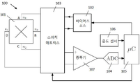
본 발명의 실시예에 따른 홀 센서(100)가 도 3에 도시되며, 상기 홀 센서는, 도핑된 반도체 물질로 제조되는 플레이트-형상 센서 요소와, 제 1 여기 접촉부에 연결되는 적어도 하나의 제 1 여기 노드와, 제 2 여기 접촉부에 연결되는 적어도 하나의 제 2 여기 노드와, 제 1 감지 접촉부에 연결되는 적어도 하나의 제 1 감지 노드와, 제 2 감지 접촉부에 연결되는 적어도 하나의 제 2 감지 노드를 포함하는 적어도 하나의 홀 요소(101)를 포함한다. 플레이트-형상 센서 요소는 기판 또는 웰 내에 매립되어, 제 1 pn-정션을 이용하여 기판 또는 웰로부터 분리될 수 있고, 기판 또는 웰은 제 1 고정 전압에 연결가능하다. 홀 센서(100)는 센서 노드에서 적어도 하나의 홀 요소(101)에 대한 측정을 수행할 수 있는 전자 측정 디바이스와, 여기 노드에서 적어도 하나의 홀 요소(101)에 전류를 공급하기 위한 하나 이상의 바이어스 소스(102)를 더 포함한다. 홀 센서(100)는 적어도 하나의 홀 요소(101)의 다양한 노드로 측정 전자 수단 및 바이어스 소스(102)를 스위칭하기 위한 스위치를 더 포함한다. A
특정 실시예에서, 홀 센서(100)는 아날로그-디지털 컨버터(ADC)(104), 및 컨트롤러(105)를 위한 전자 회로들을 포함한다. ADC(104)는 홀 요소(101)에 대해 수행되는 측정을 디지털 형태로 변환하는데 사용되고, 홀 요소(101)에 대해 이루어지는 다양한 측정을 컨트롤러(105)에 가용하게 한다. 컨트롤러(105)는 컴퓨팅 디바이스, 가령, 마이크로프로세서를 포함할 수 있고, 이것이 예를 들어, 마이크로컨트롤러일 수 있다. 특히, 프로그래머블 어레이 로직(PAL), 프로그래머블 로직 어레이(PLA), 프로그래머블 게이트 어레이(PGA), 특히 필드 프로그래머블 게이트 어레이(FPGA)와 같은 프로그래머블 디지털 로직 디바이스를 포함할 수 있다. 컨트롤러(105) 및/또는 ADC(104)는 홀 요소(101)를 지닌 동일 다이 상에 함께 집적될 수 있다. 컨트롤러(105)는 스위치(103)의 상태를 제어하기 위한 수단을 구비할 수 있다. In a particular embodiment,
본 발명의 실시예에 따른 홀 센서(100)는 온도 센서(106)를 더 포함할 수 있고, 상기 온도 센서는 홀 요소(101)에 가까운 온도를 측정하는 것이 바람직하다. The
본 발명의 실시예에 따른 홀 센서(100)는 적어도 하나의 홀 요소(101)로부터 제 1 판독 신호 VH를 획득하기 위한 수단을 구비하며, 상기 제 1 판독 신호 VH는 자기장에 실질적으로 의존한다. 이후, 이러한 제 1 판독 신호 VH가 어떻게 획득될 수 있는지에 관한 일부 예가 제공되지만, 본 발명은 이에 제한되지 않는다. The
홀 센서(100)는 바이어스 전류를 소싱하는 홀 요소의 제 1 여기 노드에 연결하기 위한 적어도 하나의 노드와, 바이어스 전류를 싱킹하는 홀 요소의 제 2 여기 노드에 연결하기 위한 다른 노드를 가진 바이어스 소스를 구비한다(도 3 참조). 홀 요소(101)의 제 1 여기 노드는 공급 전압에, 또는, 이러한 소싱 노드에 전류를 전달하는 전류 소스에, 연결될 수 있다. 제 2 여기 노드는 다른 고정 전압 레벨, 가령, 접지부에 내부적으로 연결될 수 있고, 또는, 전류 소스 싱킹 전류, 가령, 접지부에 연결될 수 있다. 여기는 전류-모드일 수 있고, 전압-모드일 수도 있다. 일부 실시예에서, 여기 전류를 측정하기 위한 수단이 제공된다. 임의의 특정 순간에서 홀 요소(101)의 노드 A, B, C, D 중 어느 것이 여기 노드로 기능하는지, 그리고, 어느 것이 감지 노드로 기능하는 지는 해당 순간에 스위치(103)의 구조 및 측정 셋업에 달려있다.
홀 센서(100)는 2개의 노드, 즉, 플러스 노드 및 마이너스 모드를 가진 측정 디바이스(107)를 구비할 수 있고, 차동 측정을 수행할 수 있다. 이러한 측정은 전압-모드로 실현되는 것이 바람직하지만, 대안으로서, 전류 모드로 수행될 수도 있다. The
이후 설명되는 모든 측정에서, 측정되는 전압은 측정 저항을 획득하도록, 바이어스 소스(102)를 이용하여 인가되는 전류에 의해 나누어질 수 있다. In all of the measurements described below, the measured voltage may be divided by the applied current using the
전압 측면에서 이후 정형화되는 결과는 저항, 전도성, 또는 다른 파생 양 측면에서 등가의 형태를 갖는다. The result, which is later stylized in terms of voltage, is equivalent in terms of resistance, conductivity, or other derivation.
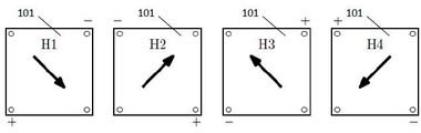
자기장에 실질적으로 의존하는 홀 요소(101)로부터의 제 1 판독 신호를 획득하는 단계는, 예를 들어, 도 4에 도시되는 홀-형 측정들 중 임의의 측정의 수행을 포함할 수 있다. 도 4는 4개의 전기 노드(각각은 홀 요소(101) 상의 일 접촉부에 대응하며 연결됨)를 포함하는 수평 홀 요소에 대해 이루어지는 측정을 도시한다. 측정은, 역시 적어도 4개의 전자 노드를 또한 가진, 수직 홀 소자에 마찬가지로 동일하게 적용될 수 있다(그러나 여기서 일 노드는 홀 요소(101) 상에 하나보다 많은 접촉부를 포함할 수 있음). Obtaining the first read signal from the
두 접촉부 사이에 그려진 화살표는 이러한 접촉부들을 전류 접촉부로 식별하며, 전류는 화살표의 꼬리에서 홀 요소(101)에 들어가고, 화살표의 머리에 의해 가리켜지는 접촉부를 떠난다. 따라서 화살표는 플레이트 내의 전류 흐름 방향을 개략적으로 표시한다. 도 3에 도시되는 구조에서, 스위치는 그 후 바이어스 소스의 소싱 노드가 홀 프레이트 노드(여기에서 전류가 홀 요소(101)에 들어감)에 연결되고, 바이어스 소스의 싱킹 노드가 홀 플레이트 노드(여기에서 전류가 홀 요소(101)를 떠남)에 연결되도록 작동된다. The arrow drawn between the two contacts identifies these contacts as current contacts, which enter the
도시되는 각각의 구조에서, 2개의 나머지 접촉부가 감지 접촉부다. 감지 접촉부들 간에 전압차가 측정되며, 이는 플러스 부호로 표시되는 접촉부에서의 전압과, 마이너스 부호로 표시된 접촉부의 전압의 차이다. 도 3에 도시되는 구조에서, 스위치(103)는 측정 디바이스(107)의 플러스 노드가 플러스 부호로 표시된 홀 플레이트 노드에 연결되고, 측정 디바이스(107)의 마이너스 노드가 마이너스 부호로 표시된 홀 플레이트 노드에 연결되도록 작동된다. In each structure shown, the two remaining contacts are sense contacts. A voltage difference between the sensing contacts is measured, which is the difference between the voltage at the contact point indicated by the plus sign and the voltage at the contact point indicated by the minus sign. In the structure shown in Fig. 3, the
홀-형 측정은 홀 요소(101)의 에지를 따름으로써 형성되는 순서로 노드들을 살필 때, 2개의 연이은 노드들이 서로 다른 기능을 갖도록 하는 것을 추가의 특징으로 한다 - 즉, 감지용으로 사용되는 홀 요소 노드가 전류 공급용 홀 요소 노드와 교번된다. 접촉부, 따라서, 관련 노드들이 플레이트-형상 센서 요소의 에지에 위치할 때, 그 순서가 명확히 규정되며, 연이은 노드들은 특정 방향으로 플레이트-형상 센서 요소의 에지에 이어질 때 서로 인접한 노드다. 노드들이 특정-형상 센서 요소의 에지 상에 위치하지 않을 때, 그 순서가 결정될 필요가 있다. 이는 플레이트의 에지 상에 모든 접촉부가 위치할 때까지 플레이트 영역을 감소시킴으로써 이루어질 수 있고, 이는 다시 플레이트의 "새 에지"에 이어질 때 그 순서를 결정할 수 있게 한다. The hall-shaped measurement is further characterized in that, when the nodes are examined in the order in which they are formed by following the edge of the
도 4에 도시되는 구조에 따른 4개의 홀-형 판독 신호가 Vh,1, Vh,2, ...Vh,4로 표시된다. 이러한 측정치들은 VH에 대해 사용될 수 있다. 이러한 홀-형 측정치 각각은 관련된 오프셋 Voi를 가지며, 이는 자기장 부재시(즉, B=0) 획득되는 측정 결과다: The four hole-type read signals according to the structure shown in Fig. 4 are represented by Vh, 1 , Vh, 2 , ... , Vh, 4 . These measurements can be used for V H. Each of these hall-type measurements has an associated offset V oi , which is the measurement result obtained in the absence of a magnetic field (i.e., B = 0)
![]()
![]()
자기장 B에 실질적으로 의존하는 홀 요소(101)로부터의 판독 신호를 획득하는 단계는, 서로 다른 홀-형 측정치들의 평균화를 포함할 수 있다. 이러한 평균화는 투-페이즈 스피닝 및 포-페이즈 스피닝의 경우에서와 같이, 순차적으로 획득되는 홀-형 측정치들을 수반할 수 있다. 대안으로서 또는 이와 조합하여, 이러한 평균화는 기하학적 스피닝의 경우와 같이 적어도 2개의 홀 플레이트의 상호연결에 대해 이루어지는 홀-형 측정치들을 또한 수반할 수 있다. Obtaining the read signal from the
본 발명의 실시예에서, VH 신호는 단일 홀 요소의 포-페이즈 스피닝에 의해 획득될 수 있다. 그 후 VH는 4개의 홀-형 판독치(Vh,1, Vh,2, ... Vh,4)의 평균에 대응한다:In an embodiment of the present invention, the V H signal can be obtained by four-phase spinning of a single hall element. V H then corresponds to the average of the four Hall-type readings (V h, 1 , V h, 2 , ... V h, 4 )

제 1 판독 신호 VH는 2개의 성분으로 분해될 수 있다:The first read signal V H can be decomposed into two components:

첫번째 항(VO)은 오프셋에 대응하고, 두번째 항 S·B는 자기 성분이다(S는 자기 감도를 표시).The first term (V O ) corresponds to the offset and the second term S · B is the magnetic component (S indicates the magnetic sensitivity).
본 발명의 실시예에 따른 홀 센서(100)는, 자기장 B에 실질적으로 독립적인, 그리고, 제 1 판독 신호 VH에 대한 오프셋 VO의 예측에 사용되는, 적어도 하나의 홀 요소(101)로부터의 제 2 판독 신호 VP를 획득하기 위한 수단을 또한 구비한다. 이후, 일부 예는 이러한 제 2 판독 신호 VP가 어떻게 획득될 수 있는지의 일부 예가 제공되지만, 발명은 이에 제한되지 않는다. The
홀-형 측정치들은 자기장 B에 의존하기 때문에 제 2 판독 신호 VP로 직접 사용될 수 없다. 그러나, 적어도 2개의 홀-형 측정치들과 선형 조합을 이룸으로써, 자기장으로 인한 성분이 소거될 수 있다. 한 예로서, 2개의 홀-형 측정치들 간의 차이가 다음과 같이 나타날 수 있다:The hole-type measurements can not be used directly as the second read signal V P because they depend on the magnetic field B. [ However, by making a linear combination with at least two Hall-type measurements, the component due to the magnetic field can be erased. As an example, the difference between the two hole-type measurements may appear as:
![]()
![]()
이때, ![]()
![]()
![]()
![]()

따라서, 이러한 조건 하에서, VP는 자기장에 실질적으로 독립적이고, 홀-형 측정 중 나타나는 오프셋에 명확하게 관련된다. 자기 감도가 정확히 동일하지 않지만 일정하게 유지되기 때문에, Vh,i 및 Vh,j의 약간 다른 선형 조합을 이용하여 자기 성분을 소거시킬 수 있다. 이는 감도 비를 결정하기 위해 교정 측정을 요구할 것이라고 예상된다. Thus, under these conditions, V P is substantially independent of the magnetic field and is clearly related to the offset appearing during the hole-type measurement. Since the magnetic sensitivity is not exactly the same but is kept constant, magnetic components can be erased using slightly different linear combinations of V h, i and V h, j . This is expected to require calibration measurements to determine the sensitivity ratio.
홀-형 측정의 선형 조합의 두번째 예는 다음에 따라 모두 4개의 홀-형 판독치를 조합함으로써 획득된다:A second example of a linear combination of hall-type measurements is obtained by combining all four hall-type readings according to:

동일한 자기장이 개별 측정 중 존재한다고 다시 가정하고, 자기 감도가 동일하다고 가정하면, 수식 (3)이 자기장 B에 실질적으로 독립적이고 다음과 같이 주어짐을 쉽게 도출할 수 있다:Assuming that the same magnetic field is present during the individual measurements and assuming that the magnetic sensitivities are the same, it can be easily deduced that equation (3) is substantially independent of magnetic field B and given as:

이는 평균 순수 오프셋 Vraw에 대응한다. This corresponds to the average pure offset V raw .
적어도 2개의 (밀접하게 이격된) 홀 플레이트들이 사용될 경우, "홀-측정치의 교번 기하학적 스피닝"(altered geometric spinning of Hall-Measurements)라 불리는 기술이 적용될 수 있다. 이러한 경우에, 홀 플레이트는 자기 성분들을 소거시키는 방식으로 상호연결된다. 이는 각각의 홀 플레이트의 2개의 노드들을 전기적으로 연결하는 스위치를 제공함으로써 실현된다. 도 5의 상부는 하나의 홀-형 구조에 하나씩 2개의 홀 플레이트의 제 1 예를 제공하며, 여기 및 감지 모두가 직렬로 놓인다. 도 5의 하부는 하나의 홀-형 구조에 하나씩 2개의 홀 프레이트의 두번째 예를 제공하며, 여기 및 감지 모두가 병렬로 배치된다. 가령, 감지 신호의 직렬 연결과 여기의 병렬 연결과 같은, 조합이 또한 이루어질 수 있다. "홀-측정의 교번 기하학적 스피닝"의 장점은 자기 성분이 시간 상의 동일 순간에 외부 장에 대응한다는 점이다. 그 후 자기장 성분의 소거는 개별 홀 요소들 간의 감도의 우수한 정합에 주로 의존한다. When at least two (closely spaced) hole plates are used, a technique called " altered geometric spinning of Hall-Measurements " may be applied. In this case, the hole plate is interconnected in such a way as to erase magnetic components. This is realized by providing a switch that electrically connects two nodes of each hole plate. The top of Fig. 5 provides a first example of two hole plates, one for each hole-type structure, both excitation and sensing being placed in series. The bottom of Fig. 5 provides a second example of two hole plates, one for each hole-type structure, both excitation and sensing being arranged in parallel. For example, a combination such as a series connection of sense signals and a parallel connection here can also be made. The advantage of "alternating geometric spinning of hall-measurements" is that magnetic components correspond to external fields at the same instant in time. The erasure of the magnetic field component then depends mainly on the good match of the sensitivity between the individual Hall elements.
본 발명의 실시예에 따르면, 자기장에 실질적으로 독립적인 홀 요소(101)로부터의 제 2 판독 신호를 획득하는 단계는, 도 6에 도시되는 "반데포"(van der Pauw)-형(VDP) 측정들 중 임의의 측정의 수행을 포함할 수 있다. 도면은 4개의 전기 노드(각각은 홀 요소 상의 하나의 접촉부에 대응함)를 포함하는 수평 홀 요소(101) 상에서 이루어지는 측정을 도시한다. 측정은 역시 적어도 4개의 전기 노드를 갖는 수직 홀 디바이스에 동등하게 적용될 수 있다(하지만 이 경우 일 노드가 홀 요소 상의 하나보다 많은 접촉부를 포함할 수 있다). According to an embodiment of the present invention, the step of acquiring a second read signal from the
2개의 접촉부 사이에 그려진 화살표는 이러한 접촉부들을 전류 접촉부로 식별하고, 화살표의 꼬리부에서 전류가 홀 요소에 들어오고, 화살표 머리에 의해 가리켜지는 접촉부에서 전류가 빠져나간다. 따라서 화살표는 플레이트 내 전류 흐름 방향을 개략적으로 표시한다. 도 3에 도시되는 본 발명의 실시예에 따른 예시적 디바이스에서, 그 후 스위치(103)는, 바이어스 소스(102)의 소싱 노드가 (전류가 홀 요소(101)로 들어가는) 홀 플레이트 노드에 연결되고, 바이어스 소스(102)의 싱킹 노드가 (전류가 홀 요소(101)를 떠나는) 홀 플레이트 노드에 연결되도록, 작동된다. The arrow drawn between the two contacts identifies these contacts as current contacts, the current at the tail of the arrow enters the Hall element, and the current exits at the contacts pointed by the arrowhead. Thus, the arrows schematically indicate the current flow direction in the plate. In an exemplary device according to an embodiment of the present invention shown in Figure 3, the
도시되는 각각의 구조에서, 2개의 나머지 접촉부는 감지 접촉부다. 감지 접촉부들 사이에서 전압차가 측정되는데, 이는 플러스 부호로 표시되는 접촉부에서의 전압과 마이너스 부호로 표시되는 접촉부의 전압의 차이다. 도 3에서, 스위치(103)는, 측정 디바이스(107)의 플러스 노드가 플러스 부호로 표시된 홀 플레이트 노드에 연결되고, 측정 디바이스(107)의 마이너스 노드가 마이너스 부호로 표시된 홀 플레이트 노드에 연결되도록 작동된다. In each structure shown, the two remaining contacts are sense contacts. A voltage difference between the sensing contacts is measured, which is the difference between the voltage at the contact portion indicated by the plus sign and the voltage at the contact portion indicated by the minus sign. 3, the
VDP-형 측정은 플레이트-형상 센서 요소의 에지를 따름으로써 형성되는 순서로 노드들을 살필 때, 동일 기능 - 이 기능은 여기 또는 감지를 위한 기능임 - 을 가진 노드들이 연이어 나타나는 것을 추가의 특징으로 한다. 접촉부가, 따라서, 관련 노드가, 플레이트-형상 센서 요소의 에지에 위치할 때, 그 순서가 명확히 규정되고, 연이은 노드들은 특정 방향으로 플레이트-형상 센서 요소의 에지를 따를 때 서로에 인접한 노드다. 노드들이 플레이트-형상 센서 요소의 에지 상에 위치하지 않을 때, 그 순서가 결정될 필요가 있다. 이는 모든 접촉부들이 플레이트의 에지 상에 위치할 때까지 플레이트-형상 센서 요소의 영역을 축소시킴으로써 실현될 수 있고, 이는 다시 플레이트의 "새 에지"에 이어질 때 그 순서를 결정할 수 있게 한다. 제 2 판독 신호 VP를 도출하기 위한 "반데포"-형 측정을 이용할 때의 장점은 이들이 자기장 존재에 실질적으로 무감하다는 점이다. 그 이유는 홀 효과가 동일한 방식으로 두 감지 접촉부 모두의 전위를 변화시키기 때문이며, 이는 이러한 VDP 측정 중 측정되는 전압차에 거의 영향이 없음을 의미한다. 따라서, VDP-형 측정 수행에 걸리는 시간 역시 자기장이 일정하게 유지되어야 하는 요건에 의해 구속되지 않는다. The VDP-type measurement is further characterized by the fact that when nodes are examined in the order they are formed by following the edge of the plate-shaped sensor element, the nodes having the same function - this function being the excitation or sensing function - . The order is clearly defined when the contact, and therefore the associated node, is located at the edge of the plate-shaped sensor element, and the successive nodes are nodes adjacent to each other when following the edge of the plate-shaped sensor element in a particular direction. When the nodes are not located on the edge of the plate-shaped sensor element, the order needs to be determined. This can be realized by reducing the area of the plate-shaped sensor element until all of the contacts are located on the edge of the plate, which again makes it possible to determine the order of the "new edge" of the plate. The advantage of using an " anti-depo "-type measurement to derive the second read signal V P is that they are substantially insensitive to the presence of a magnetic field. This is because the Hall effect changes the potential of both sense contacts in the same way, which means that there is little effect on the voltage difference measured during this VDP measurement. Thus, the time taken to perform the VDP-type measurement is also not constrained by the requirement that the magnetic field should remain constant.
본 발명의 특정 실시예에서, 홀 요소(101)로부터 제 2 판독 신호 VP를 획득하는 단계 - 제 2 판독 신호 VP는 자기장 B에 실질적으로 독립적임 - 는, 2개의 "반데포"-형 측정치의 차를 취하는 단계를 포함할 수 있다. 이 차이는 순차적으로 획득되는 "반데포"-형 측정치를 수반할 수 있다. 대안으로서, 이러한 차이는 적어도 2개의 홀 플레이트(101)의 상호연결에 대해 단일 측정을 수행함으로써 획득될 수 있고, 각각의 개별 홀 요소(101)는 "반데포"-형 구조에 있다. 한 예가 도 7에 제공된다. In a particular embodiment of the invention, the step of obtaining a second read signal V P from the
본 발명의 실시예에서, 홀 요소(101)로부터 제 2 판독 신호 VP를 획득하는 단계 - 상기 제 2 판독 신호 VP는 자기장 B에 실질적으로 독립적임 - 는 앞서 설명된 가능성들 중 임의의 것을 통해 획득되는 판독 신호 VP들의 평균화를 포함할 수 있다. 이는 멀티-페이즈 스피닝과 유사한 동일 타입의 구조에 대한 평균화를 포함한다. In an embodiment of the present invention, the step of obtaining a second read signal V P from the
본 발명의 실시예에서, 자기장에 실질적으로 독립적인 홀 요소(101)로부터의 제 2 판독 신호 VP 획득 단계는, 다음의 수식에 따른 8개의 VDP 측정들의 선형 조합이 결정을 포함할 수 있다:In an embodiment of the present invention, the second reading signal V P acquisition step from the

또는 or

우리는 수식 (2)에 따라 자기 성분 B에 관한 항 및 오프셋 VO에서 분해될 수 있는 제 1 판독 신호 VH가 이제 가용하다. 시스템이 VO 를 추정할 수 있을 경우, 오프셋-보상 판독치를 획득할 수 있다. We now have a term for the magnetic component B according to equation (2) and a first read signal V H that can be decomposed at offset V O is now available. If the system is able to estimate V o , an offset-compensated reading can be obtained.
본 발명의 실시예에 따른 홀 센서(100)에는 제 2 판독 신호 VP로부터 Vo의 추정치 ![]()
![]()
![]()
![]()
이는 자기장 결정에 또한 사용될 수 있다. 수식 (7)에 따라 오프셋-보상 신호를 획득할 가능성이 많다. 도 3에 도시되는 것과 같은 유연한 구조의 경우, 이는 디지털 감산으로 컨트롤러(105)에 의해 구현될 수 있다. 동일한 효과가 다른 방식으로, 가령, 당 업자가 쉽게 이해할 수 있듯이, 프론트-엔드에서 보상 신호를 주입함으로써, 실현될 수 있다. 오프셋 보상 신호를 수행하기 위한 신호의 예측이 발명의 일부분인 상황에서, 오프셋 보상 신호 획득을 위한 이러한 신호 인가는 당 업자의 통상의 지식 내에 있다. It can also be used for magnetic field determination. There is a high possibility of obtaining an offset-compensated signal according to Equation (7). In the case of a flexible structure such as that shown in Fig. 3, this can be implemented by the
VDPVDP 측정으로부터 홀-형 오프셋 예측 Predicted hole-type offset from measurement
선형 홀 요소의 이상화된 경우에, 홀-형 판독의 오프셋들 간에 유도될 수 있는 소정의 수학적 관계가 존재하며, VDP 측정치들의 차이가 가능한 제 2 판독 신호 VP로 사용하기 위해 제안된다. 특히, 약한 비선형 플레이트의 경우에, VH의 오프셋 보상을 위해 우수한 예측기(predictors)가 유도될 수 있다. In the idealized case of a linear Hall element, there is a certain mathematical relationship that can be derived between offsets of the Hall-type readout, and a difference in VDP measurements is suggested for use as a possible second read signal V P. In particular, in the case of weak nonlinear plates, good predictors can be derived for offset compensation of V H.
2개의 "반데포 측정" 및 오프셋 측정이 선형 관계임이, 등방성 물질에 대한 L. J. van der Pauw, "A method of measuring specific resistivity and Hall effect of discs of arbitrary shape," Philips Research Reports, vol. 13, no. 1, 1958, 또는 이방성 물질에 대한 R. T. H. Shibata, "A potential problem for point contacts on a two-dimensional anisotropic medium with an arbitrary resistivity tensor," J. Appl. Phys., vol. 66, no. 10, November 1989 로부터 유도될 수 있다. 따라서, 획득되는 증거는 이러한 공개본에서 암묵적으로 제시되는 부가 조건에 여전히 좌우된다 - 가령, 물질이 구조를 통해 균일한 성질을 가진다고 가정된다. Two "anti-depot measurements" and offset measurements are linear, L. J. van der Pauw, " A method of measuring specific resistivity and Hall effect of discs of arbitrary shape, " 13, no. 1, 1958, or R. T. H. Shibata for anisotropic materials, "A Potential Problem for Point Contacts on a Two-Dimensional Anisotropic Medium with an Arbitrary Resistivity Tensor," J. Appl. Phys., Vol. 66, no. 10, November 1989. < / RTI > Thus, the evidence obtained is still dependent on the additional conditions implicitly presented in these open publications - for example, assuming that the material has uniform properties throughout the structure.
발명자는 불균일 물질에 대해 동일한 관계가 유효하게 유지됨을 유도하였다. 이러한 유도는 플레이트의 에지에 위치하지 않는 접촉부와, 연장된 접촉부를 갖는 홀 플레이트에 대해 또한 유효하다. 윤곽이 이후 제시된다. The inventor has suggested that the same relationship remains valid for heterogeneous materials. This induction is also effective for the contact portion not located at the edge of the plate and for the hole plate having the extended contact portion. The outline is presented later.
제로 자기장에서, 선형 홀 플레이트가 4개의 노드에서 전압 및 전류를 관계시키는 저항-매트릭스에 의해 설명된다. 일반적인 비대칭 홀 플레이트는 제로 자기장에서 6개의 독립적인 파라미터를 갖고, 이는 "Limits of Offset Cancellation by the Principle of Spinning Current Hall Probe", Proceedings of IEEE Sensors, Oct. 2004, pp.1117-1120에 소개되어 있고, 본 발명에서 참고자료로 포함된다. 직관적 연산을 이용하여, 홀-기반 측정 중 오프셋 수식이 (6개의 독립 파라미터의 함수로) 얻어졌다. 전류-바이어스로, ![]()
![]()
![]()
![]()
![]()
![]()
![]()
![]()
따라서, 선형 홀 요소(101)의 경우, 이븐-페이즈(even-phase) VDP-형 측정 중 임의의 값과, 아드-페이즈(odd-phase) VDP-형 측정 중 임의의 값 간의 차이는 홀 측정의 순수 오프셋과 동일하다(엑스트라 마이너스 부호를 가질 가능성이 있음). 한 예로서, 도 8에 도시되는 수직 홀 플레이트에 대한 측정을 참조한다. Thus, for
유도되는 수식은 선형 물질용으로만 이론적으로 적용된다. 이들은 비선형 홀 요소의 경우에 대략 유효하게 유지되며, 이는 소정의 전압-의존적 비선형성을 통상적으로 나타낸다. 발명자는 VDP-기반 오프셋 예측의 여러가지 값들의 평균화에 의해, 홀-형 판독 중 발생하는 평균 오프셋에 대한 추정치를 얻을 수 있다는 것을 발견하였다. 예를 들어, 수식 (5)는 수식 (3)으로부터 약간 벗어나며, 전압-의존적 비선형성이 존재할 때에도 수식 (5)가 수식 (3)으로부터 약간 벗어난다는 점이 입증된 바 있다. 수식 (5) 이용의 장점은, 각각의 개별 VDP 측정이 자기장에 실질적으로 독립적임에 반해 수식 (3)은 자기 성분의 소거를 필요로한다는 점이다. 수식 (1)의 VH와 연관된 잔류 오프셋과 수식 (6) 간에 우수한 상관도를 예측하기 위한 이론적 주장이 또한 존재한다. The derived equations apply theoretically only for linear materials. These remain approximately valid in the case of nonlinear Hall elements, which typically represent a certain voltage-dependent nonlinearity. The inventors have found that by averaging various values of the VDP-based offset prediction, an estimate can be obtained for the average offset occurring during the Hall-type reading. For example, equation (5) deviates slightly from equation (3) and has proven that equation (5) deviates slightly from equation (3) even in the presence of voltage-dependent nonlinearity. An advantage of using Equation (5) is that each individual VDP measurement is substantially independent of the magnetic field, whereas Equation (3) requires the erasure of magnetic components. There is also theoretical argument for predicting a good correlation between the residual offset associated with V H of equation (1) and equation (6).

따라서, 수식 (6)은 수식 (8)에 의해 규정되는 포-페이즈 스피닝 후 잔류 오프셋 VO의 더욱 직접적인 추정을 제공하는 오프셋-관련 신호를 제공할 수 있다. Thus, Equation (6) can provide an offset-related signal that provides a more direct estimate of the residual offset V O after for-phase spinning as defined by equation (8).
선형 예측Linear prediction
일부 경우에, 제 2 판독 신호 VP는 교정 수행없이, 제 1 판독 신호 VH에 대한 오프셋 VO를 예측하는데 직접 사용될 수 있다. 예를 들어, 단일 홀-형 측정의 수행을 고려할 때(가령, VH=Vh1), 그리고 ![]()
![]()
![]()
![]()
위 추정 규칙 ![]()
![]()
![]()
![]()
추정 법칙은 오프셋 VO와 예측 VP 신호 간에 잘 알려진 상관 관계가 존재할 때 유리하게 이용될 수 있다. 오프셋-관련 신호가 동일 세트의 원인에 의해 모두 영향받기 때문에, 이러한 상관관계가 기대될 수 있다. 이러한 상관 관계는 홀 디바이스에 대해 수행되는 특성화 측정으로부터 결정될 수 있다. 그러나, VO 및 VP의 크기가 크게 다를 수 있다. 이는 예를 들어, VP가 수식 (3)에 의해 규정되는 평균 순수 오프셋이거나 수식 (5)에 의해 주어지는 VDP-기반 예측인 경우이고, VO는 포-페이즈 스피닝 후 수식 (14)에 의해 주어지는 잔류 오프셋이다. 이러한 경우에, 작은 팩터 b가 추정 규칙에 필요하다. The estimation rule can be advantageously used when there is a well-known correlation between the offset V O and the predicted V P signal. Since the offset-related signals are all affected by the same set of causes, this correlation can be expected. This correlation can be determined from the characterization measurements performed on the Hall device. However, the magnitudes of V O and V P can be significantly different. This is the case, for example, where V P is the mean pure offset specified by equation (3) or VDP-based prediction given by equation (5), and V O is the post- Is the residual offset. In this case, a small factor b is required for the estimation rule.
오프셋의 추정은 오프셋 예측의 파라미터 a 및 b를 온도-의존적으로 만듦으로써 추가적으로 개선될 수 있다. The estimation of the offset can be further improved by making the parameters a and b of the offset prediction temperature-dependent.
교정을 통한 예측 최적화Predictive optimization through calibration
수식 (9)에 의해 규정된 선형 예측기의 성능을 개선시키기 위해, 파라미터 a 및/또는 b가 교정을 이용하여 각각의 개별 홀 센서(100)에 대해 최적화될 수 있다. In order to improve the performance of the linear predictor defined by equation (9), the parameters a and / or b may be optimized for each
오프셋 VO가 온도에만 의존하고 재현가능할 경우, 알려진 자기장, 바람직한 경우 제로 자기장에서, 교정-측정 중 결정될 수 있다. 이는 그 후 수식 (9)에서 a-항으로 취급될 수 있고, 이는 오프셋을 완벽하게 보상할 것이다. b-항은 필요없을 것이고, VP를 얻기 위해 측정을 할 필요도 없다. 그러나, 오프셋 드리프트를 논의할 때 앞서 언급한 바와 같이, 일부 오프셋 소스는 온도의 함수로 부분적으로만 재현가능하고, 그러나 예를 들어, 패키지-유도 응력에 또한 좌우된다. 본 발명의 실시예에 따른 교정 기법은 발생하는 이와같이 부분적으로 재현불가능한 효과를 보상하기 위한 수단을 제공한다. If the offset V O depends only on temperature and is reproducible, it can be determined during calibration-measurement in a known magnetic field, preferably in a zero magnetic field. This can then be treated as a- in Eq. (9), which will completely compensate for the offset. The b-term will not be necessary, nor does it need to be measured to obtain V P. However, as discussed above in discussing offset drift, some offset sources are only partially reproducible as a function of temperature, but also on package-induced stresses, for example. The calibration technique in accordance with embodiments of the present invention provides a means for compensating for such partially non-reproducible effects that occur.
평면형 폴 플레이트 내의 오프셋은 통상적으로, σ로 표시되는 하나의 특정 응력 성분에만 주로 의존한다. 예를 들어, <101> 플랫을 따라 정렬되는 (100) 웨이퍼 상의 스퀘어 수평 홀 요소는 평면-내 차동 응력 σ = σD = σxx - σyy에 민감하고, 반면 이러한 오프셋은 평면-내 등방성 응력 σI = σxx + σyy에 직접 영향받지 않고, 평면-내 전단 응력 σxy에 의해서도 영향받지 않는다. The offset in the planar pole plate typically depends only on one particular stress component, denoted by [sigma]. For example, a square horizontal hole element on a (100) wafer aligned along a <101> flat is sensitive to the in-plane differential stress σ = σ D = σ xx - σ yy , It is not directly affected by σ I = σ xx + σ yy and is not affected by the in-plane shear stress σ xy .
실제 오프셋 VO 및 오프셋-예측 신호 VP에서 알려지지 않은 응력의 영향이 이제 분리될 수 있다. 작은 효과가 예상될 수 있기 때문에, 선형 근사가 사용될 수 있다:The influence of the unknown stress at the actual offset V O and the offset-prediction signal V P can now be separated. Since a small effect can be expected, a linear approximation can be used:
![]()
![]()
![]()
![]()
여기서, VO ,rep(T) 및 VP,rep(T)는 (항상 온도와 동일한 방식으로 변하는) 재현가능 성분을 나타내고, α(T) 및 β(T)는 사용되는 물질에 좌우되는, 온도-의존적 응력-의존성을 가질 수 있다. Here, V O , rep (T) and V P, rep (T) represent reproducible components (which always change in the same way as temperature) and α (T) and β (T) And may have a temperature-dependent stress-dependency.
기준 신호 획득을 위한 교정 과정Calibration process for reference signal acquisition
이제 오프셋 보상을 위해 홀 센서의 작동 중 사용될 2개의 기준 곡선(VOref(T) 및 VPref(T))을 결정하기 위한 제 1 생산-시간 교정 과정이 설명된다. A first production-time calibration procedure for determining two reference curves (V Oref (T) and V Pref (T)) to be used during operation of the Hall sensor for offset compensation is now described.
센서 시스템은 이 설명 단락의 종료시 표에 설명되는 상태들 중 하나와 같은, 기준 상태에 놓인다. 한 예로서, 센서 시스템은 최종 패키징된 형태로 놓일 수 있다. 센서 시스템은 n = 1...N에 대하여 다수의 온도 Tn에 놓인다. 자기장은 알려져있다고 가정하고, 바람직한 경우 자기장이 0이다. 각각의 온도 Tn에서, 시스템은 제 1 판독 신호 VHref ,n의 측정치를 제공하고, 이로부터 알려진 자기장에 대응하는 자기 성분을 빼서 (잔류) 오프셋 VOref ,n을 얻을 수 있고, 시스템은 제 2 판독 신호 VPref,n의 측정치를 제공한다. 자기장이 0으로 알려진 경우에(가령, 제로-가우스 챔버에 센서를 배치함으로써), 제 1 판독 신호가 (잔류) 오프셋 VOref ,n에 직접 대응한다. 온도 Tn에 대한 측정치는 온-칩 온도 센서로부터 또는 외부 장비에 의해 측정될 수 있다. 획득되는 측정치 VHref ,n (또는 가능하다면 VOref ,n) 및 VPref ,n 은 가령, 피팅을 통해, 또는 표-기반 보간을 이용하여, 보간 형태로 변환될 수 있고, 2개의 기준 곡선: VOref(T) 및 VPref(T)을 제시한다. The sensor system is in a reference state, such as one of the states described in the table at the end of this description paragraph. As an example, the sensor system may be placed in a final packaged form. The sensor system is placed at a number of temperatures Tn for n = 1 ... N. Assuming that the magnetic field is known, the magnetic field is preferably zero. At each temperature Tn, the system provides a measure of the first read signal V Href , n and subtracts the magnetic component corresponding to the known magnetic field from it (residual) to obtain the offset V Oref , n , Provides a measure of read signal V Pref, n . If the magnetic field is known as zero (e.g., by placing the sensor in a zero-Gaussian chamber), the first read signal directly corresponds to the (residual) offset V Oref , n . Measurements of temperature Tn may be measured from the on-chip temperature sensor or by external equipment. The obtained measurements V Href , n (or possibly V Oref , n ) and V Pref , n can be transformed into an interpolated form, for example, through fitting, or using table-based interpolation, V Oref (T) and V Pref (T).
위 교정 단계 중, 알려지지 않은 온도-의존적 응력 레벨 σ=σref(T)가 존재한다. 따라서, 2개의 기준 신호가 대략 다음과 같이 주어진다:During the above calibration step, there is an unknown temperature-dependent stress level σ = σ ref (T). Thus, two reference signals are given approximately as follows:
![]()
![]()
![]()
![]()
다른 물리적 효과가 오프셋에 부분적으로 예측불가능한 결과를 야기하는 경우에, 동일한 교정 과정이 사용될 수 있다. The same calibration procedure can be used if different physical effects cause partially unexpected results in the offset.
기준 신호를 이용한 온-칩 보상On-chip compensation using reference signal
본 발명의 실시예에서, 홀 센서 시스템은 다음을 이용하여 수식 (9) 타입의 선형 오프셋 예측기를 구현한다:In an embodiment of the present invention, the Hall sensor system implements a linear offset predictor of the type (9) using:
![]()
![]()
이러한 예측기는 또한 다음과 같이 표현될 수 있다:This predictor can also be expressed as: < RTI ID = 0.0 >
![]()
![]()
여기서, 기준 신호 VOref(T) 및 VPref(T)는 교정 과정 중 결정되는 값과 실질적으로 동일하다. 신호 VP는 제 2 판독 신호이고, 이는 온도 T의 명시적으로 알지 못하면서도 측정될 수 있으나, 통상적으로 홀 요소의 온도 T에 의존한다. 작동 중, 자기장은 통상적으로 0이 아니지만, 이는 자기장에 실질적으로 독립적인 것으로 가정되는 제 2 판독 신호 VP에 거의 영향을 미치지 않는다. 기준 신호 VOref(T) 및 VPref(T)는 소정의 비휘발성 형태로, 가령, EPROM 메모리를 이용하여, 칩 상에 저장되는 교정 데이터에 기초하여, 명시적으로 아날로그 신호로, 가령, 전압 또는 전류 또는 펄스-폭으로 생성될 수 있다. Here, the reference signals V Oref (T) and V Pref (T) are substantially the same as those determined during the calibration process. The signal V P is the second read signal, which can also be measured without explicit knowledge of the temperature T, but typically depends on the temperature T of the Hall element. During operation, the magnetic field is typically not zero, but it has little effect on the second read signal V P , which is assumed to be substantially independent of the magnetic field. The reference signals V Oref (T) and V Pref (T) can be expressed in a predetermined nonvolatile form, for example, using an EPROM memory, explicitly as an analog signal, based on calibration data stored on the chip, Or current or pulse-width.
기준 신호 또는 이러한 신호들의 조합을 명시적으로 생성하기 위한 용도로, 서로 다른 온도 의존성을 가질 수 있는 소스들을 조합하는 회로가 사용될 수 있다. 그 후 비휘발성 정보를 이용하여, 이러한 소스들이 어떻게 조합되어 기준 신호 또는 기준 신호들의 조합을 생성하는 지를 규정할 수 있다. 온-칩 소스는 홀 요소들의 온도 T와 실질적으로 동일한 온도를 갖도록 홀 요소에 충분히 가깝게 놓인다. 이러한 기법에 따라, 온도를 명시적으로 측정함없이 기준 신호 VOref(T) 및 VPref(T)는를 생성할 수 있다. For purposes of explicitly generating a reference signal or a combination of such signals, a circuit that combines sources that may have different temperature dependencies may be used. Non-volatile information can then be used to define how these sources combine to produce a reference signal or a combination of reference signals. The on-chip source is placed sufficiently close to the Hall element to have a temperature substantially equal to the temperature T of the Hall elements. According to this technique, the reference signals V Oref (T) and V Pref (T) can be generated without explicitly measuring the temperature.
다른 실시예에서, 칩 상에 저장되는 비휘발성 교정 데이터는 표-기반 값들, 또는, 보간 함수들의 저장된 계수로 구성될 수 있다. 작동 중, 실제 온도 Ta가 측정될 수 있다. 이와 같이 측정된 실제 온도 Ta에 기초하여, 표 및/또는 보간 함수를 이용하여 기준 신호를 결정할 수 있다. 이는 가령, 도 3에 도시되는 실시예에서와 같이 컨트롤러(105)를 이용하여, 연산을 통해 실현될 수 있다. In another embodiment, the non-volatile calibration data stored on the chip may comprise table-based values, or a stored coefficient of interpolation functions. During operation, there is to be measured actual temperature T a. Based on the measured actual temperature Ta, the reference signal can be determined using the table and / or the interpolation function. This can be realized, for example, by calculation using the
대안으로서, 기준 신호 VOref(T)는 당 업자에게 알려진 형태들 중 임의의 형태로 구현될 수 있는 일상의 온도-의존적 오프셋-보상에 대응하는 것으로 간주될 수 있다. 용어 ![]()
![]()
수식 (14)의 b-팩터는 일정할 수도 있고, 온도에 의존할 수도 있다. 두번째 항에 대응하는 신호는 아날로그 방식으로 생성될 수 있고, b-팩터는 회로의 이득으로 구현된다. 다른 가능성은 가령 전압으로 아날로그 신호 1/b(T)를 명시적으로 발생시켜서, 신호 VP - VPref 를 디지털 도메인으로 변환하는 아날로그-디지털 컨버터 내 기준 신호로 이를 이용하는 것이다. 또 다른 가능성은 ADC용으로 고정 기준 전압을 이용하고, 디지털 도메인에서 이득 팩터 b를 구현하는 것이다. The b-factor of equation (14) may be constant or dependent on temperature. The signal corresponding to the second term can be generated in an analog manner, and the b-factor is implemented in the gain of the circuit. Another possibility is to explicitly generate the analog signal 1 / b (T) with a voltage, for example, to use it as a reference signal in an analog-to-digital converter that converts the signal V P - V Pref into a digital domain. Another possibility is to use a fixed reference voltage for the ADC and to implement the gain factor b in the digital domain.
제 2 교정을 통한 예측 최적화Predictive optimization through second calibration
수식 (14)의 오프셋-예측기의 b-팩터는 추가적인 교정 측정을 통해 추가로 최적화될 수 있다. 이는 제 2 생산-시간 교정 과정을 거침으로써 이루어질 수 있다. The b-factor of the offset-predictor of equation (14) can be further optimized through additional calibration measurements. This can be done by going through a second production-time calibration process.
제 2 생산-시간 교정 중, 센서 시스템은 제 2 상태에 놓이고, 제 2 상태는 예를 들어, 서로 다른 응력 레벨 σ=σsec(T)가 발생하는 점을 특징으로 한다. 본 설명의 종료부의 표에 예가 제공된다. 센서 시스템은 m = 1...M에 대하여 다수의 온도 Tm에서 다시 놓이며, 이 온도는 기준 교정 중 사용되는 온도와 같을 수도 있고 다를 수도 있다. 기준 교정 중과 유사한 측정이 이루어져서, 제 2 세트의 보간 곡선 VOsec(T) 및 VPsec(T)을 도출한다. 다음의 신호가 획득된다:During the second production-time calibration, the sensor system is placed in the second state and the second state is characterized, for example, by a different stress level σ = σ sec (T). An example is provided in the table at the end of this description. The sensor system is reset at a number of temperatures, Tm, for m = 1 ... M, which may or may not be equal to the temperature used during reference calibration. Measurements similar to those in the reference calibration are made to derive a second set of interpolation curves V Osec (T) and V Psec (T). The following signals are obtained:
![]()
![]()
![]()
![]()
온도-의존적 최적 스케일 팩터 b는 다음과 같이 유도될 수 있다:The temperature-dependent optimal scale factor b can be derived as:

공통 세트의 온도 Tn이 사용된 경우에, b(T)가 다음과 한 세트의 값(Tn, bn)의 보간으로부터 또한 발견될 수 있다:If a temperature Tn of a common set is used, b (T) can also be found from interpolation of the following set of values Tn, bn:

b(T)의 정의를 이제 수식 (12), 수식 (13), 수식 (15), 및 수식 (16)과 조합함으로써 다음의 결과를 얻을 수 있다. The following results can be obtained by combining the definition of b (T) with the equations (12), (13), (15) and (16)

이 경우 σsec(T) - σsec(T) - σref(T)가 너무 작지 않다고 가정한다. σ가 응력을 나타낼 때, 이는 2차 교정 중 응력이 기준 교정 중 응력과 충분히 달라야 함을 의미한다. 수식 (18)을 이용하여, 수식(14)의 선형 예측기가 동일 응력 레벨 σ=σref가 나타날 때 기준 교정에서 측정되는 오프셋을 정확하게 재현함을 보여주는 것은 쉬운 편이다 - 즉, ![]()
![]()
이중 교정 기법은 매우 일반적이며, 많은 흥미로운 특별한 경우들을 포함한다. 이주 일부는 다음 표에서 요약될 수 있다. Dual calibration techniques are very common and involve many interesting special cases. Some of the migration can be summarized in the following table.
물론 보조 교정 - 가령, 웨이퍼-레벨 상에서의 측정을 수반할 때 - 은, 기준 교정 - 가령, 패키징된 디바이스 상의 측정을 수반할 때 - 에 실제로 선행할 수 있다. Of course, the supplementary calibration-for example, when carrying out measurements on a wafer-level-can actually precede a reference calibration-for example, when carrying out measurements on a packaged device.
발명은 개시되는 실시예에 제한되지 않는다. The invention is not limited to the disclosed embodiments.
Claims (25)
상기 홀 센서는 도핑된 반도체 물질로 제조된 플레이트-형상 센서 요소를 가진 적어도 하나의 홀 요소를 포함하고, 상기 홀 센서는 교정 과정(calibration procedure)으로부터 획득되는 교정 데이터를 비휘발성 형태로 저장하는 온-칩 저장 수단을 더 포함하는 반도체 칩에 내장되며, 상기 방법은,
i) 결정될 오프셋(VO)을 포함하는 측정될 자기장에 실질적으로 의존하는 결과를 도출하는 제 1 기술을 이용함으로써 상기 적어도 하나의 홀 요소로부터 제 1 판독 신호(VH)를 획득하는 단계와,
ii) 자기장에 실질적으로 독립적인 그러나 상기 오프셋(VO)에 상관되는, 결과를 도출하는 제 2 기술을 이용함으로써 상기 적어도 하나의 홀 요소로부터 제 2 판독 신호(VP)를 획득하는 단계와,
iii)
오프셋 결정 방법.A method of determining an offset of a hall sensor for measuring a magnetic field,
Wherein the Hall sensor comprises at least one Hall element having a plate-like sensor element made of a doped semiconductor material, the Hall sensor having on-off storage for storing calibration data obtained from a calibration procedure in a non- - embedded in a semiconductor chip further comprising chip storage means,
i) obtaining a first read signal (V H ) from said at least one Hall element by using a first technique to derive a result that is substantially dependent on a magnetic field to be measured comprising an offset (V O ) to be determined;
ii) obtaining a second read signal (V P ) from said at least one hall element by using a second technique that is substantially independent of the magnetic field, but correlated to said offset (V O )
iii)
Method of determining offset.
온도 의존적인
오프셋 결정 방법. 2. The method of claim 1, wherein the offset prediction (
Temperature-dependent
Method of determining offset.
제 2 판독 신호(VP)의 함수로 오프셋 예측치(
오프셋 결정 방법.3. The method according to claim 1 or 2,
As a function of the second read signal (V P ), the offset prediction
Method of determining offset.
상기 교정 과정은,
제 1 세트의 온도로부터 선택되는 알려진 온도(T)에서 알려진 자기장을 갖는 환경에 홀 센서를 배치하는 단계와,
상기 제 1 세트의 온도의 각각의 온도(T)에 대하여, 제 1 기준 신호(VOref(T))로 상기 제 1 기술을 이용함으로서 획득되는 상기 제 1 판독 신호(VH)와, 제 2 기준 신호(VPref(T))로 상기 제 2 기술을 이용함으로써 획득되는 제 2 판독 신호(VP)를 레코딩하는 단계를 포함하는
오프셋 결정 방법. The method of claim 3,
The calibration process includes:
Placing a Hall sensor in an environment having a known magnetic field at a known temperature (T) selected from a first set of temperatures,
For each temperature (T) of the temperature of the first set, the first read signal (V H ) obtained by using the first technique with a first reference signal (V Oref (T) And recording a second read signal (V P ) obtained by using said second technique with a reference signal (V Pref (T)),
Method of determining offset.
교정 과정을 이용하여 파라미터 b를 결정하는 단계를 더 포함하며, 이는,
제 2 세트의 온도로부터 선택되는 알려진 온도에서 알려진 자기장을 갖는 환경에 홀 센서를 배치하는 단계와,
제 3 기준 신호(VOsec(T))로 상기 제 1 기술을 이용함으로서 획득되는 제 1 판독 신호(VH)와, 제 4 기준 신호(VPsec(T))로 상기 제 2 기술을 이용함으로써 획득되는 제 2 판독 신호(VP)를 상기 제 2 세트의 온도의 각각의 온도에 대하여 레코딩하는 단계와,
직접 측정이 가용하지 않은 온도에서 결정될 필요가 있을 때 기준 신호들이 보간된다는 가정과 함께, (VOsec - VOref) 및 (VPsec - VPref) 간의 스케일 팩터로 레코딩된 기준 신호로부터 파라미터 b를 결정하는 단계를 포함하는
오프셋 결정 방법.5. The method of claim 4,
Further comprising the step of determining the parameter b using a calibration procedure,
Placing a Hall sensor in an environment having a known magnetic field at a known temperature selected from a second set of temperatures,
By using the second technique with a first read signal V H obtained by using the first technique as the third reference signal V Osec (T) and a fourth reference signal V Psec (T) Recording the obtained second read signal (V P ) for each temperature of the second set of temperatures,
The parameter b is determined from a reference signal recorded with a scale factor between (V Osec - V Oref ) and (V Psec - V Pref ), with the assumption that reference signals are interpolated when the direct measurement needs to be determined at a temperature that is not available Step
Method of determining offset.
상기 오프셋 예측치(
오프셋 결정 방법.The method according to claim 4 or 5,
The offset prediction value (
Method of determining offset.
단계 ii)의 적어도 하나의 홀 요소로부터 제 2 판독 신호(VP)를 획득하는 단계는, 자기장 성분이 소거되도록 적어도 2개의 홀-형 측정치를 가진 판독 신호들의 선형 조합을 취하는 단계를 포함하는
오프셋 결정 방법.7. The method according to any one of claims 1 to 6,
Obtaining a second read signal (V P ) from at least one Hall element of step ii) comprises taking a linear combination of read signals with at least two Hall-type measurements such that the magnetic field component is erased
Method of determining offset.
단계 ii)의 적어도 하나의 홀 요소로부터 제 2 판독 신호(VP)를 획득하는 단계는, 개별 홀 요소들의 자기장 성분이 서로 소거되도록 적어도 2개의 이웃하는 홀 요소들을 포함하는 구조의 판독을 포함하는
오프셋 결정 방법.8. The method according to any one of claims 1 to 7,
The step of obtaining a second read signal (V P ) from at least one hall element of step ii) comprises reading a structure comprising at least two neighboring hall elements such that the magnetic field components of the individual hall elements are erased from each other
Method of determining offset.
단계 ii)의 적어도 하나의 홀 요소로부터 제 2 판독 신호(VP)를 획득하는 단계는, 복수의 이웃하는 홀 요소에 대한 기하학적 스피닝 측정으로부터 획득되는 측정 신호들의 평균화를 포함하는
오프셋 결정 방법.9. The method of claim 8,
The step of obtaining a second read signal (V P ) from at least one hall element of step ii) comprises averaging the measured signals obtained from the geometrical spinning measurements on the plurality of neighboring hall elements
Method of determining offset.
적어도 하나의 홀 요소는 적어도 4개의 노드를 포함하고, 단계 ii)의 적어도 하나의 홀 요소로부터 제 2 판독 신호(VP)를 획득하는 단계는, 플레이트-형상 센서 요소의 에지를 따름으로써 형성되는 순서로 노드들을 살필 때 동일 기능을 가진 노드들이 연이어 나타나도록 홀 요소의 반데포-형 측정 셋업으로 측정 신호들을 획득하는 단계들을 포함하고, 상기 제 2 판독 신호(VP)는 적어도 하나의 홀 요소에 대한 2개의 반데포-형 측정을 차분(differencing)함으로써 획득되는
오프셋 결정 방법.7. The method according to any one of claims 1 to 6,
Wherein the at least one hole element comprises at least four nodes and the step of obtaining a second read signal (V P ) from at least one hole element of step ii) comprises the step of: And obtaining measurement signals in an anti-depot-type measurement setup of the Hall element such that nodes having the same function appear consecutively when examining the nodes in order, wherein the second read signal (V P ) comprises at least one Hall element Lt; RTI ID = 0.0 > demodulation < / RTI >
Method of determining offset.
2개의 반데포-형 측정을 차분하는 단계는 순차적으로 획득되는 2개의 반데포 측정을 차분하는 단계를 포함하는
오프셋 결정 방법. 11. The method of claim 10,
The step of subtracting the two anti-depot-type measurements includes the step of subtracting the two anti-depot measurements sequentially obtained
Method of determining offset.
2개의 반데포-형 측정을 차분하는 단계는, 적어도 2개의 홀 플레이트의 상호연결에 대한 단일 측정을 수행함으로써 획득되는
오프셋 결정 방법.11. The method of claim 10,
The step of subtracting the two anti-depot-type measurements is obtained by performing a single measurement of the interconnections of at least two hole plates
Method of determining offset.
단계 ii)의 적어도 하나의 홀 요소로부터 제 2 판독 신호(VP)를 획득하는 단계는, 적어도 하나의 홀 요소에 대한 복수의 반데포-형 측정들의 선형 조합을 취하는 단계를 포함하는
오프셋 결정 방법.13. The method according to any one of claims 10 to 12,
Obtaining a second read signal (V P ) from at least one hall element of step ii) comprises taking a linear combination of a plurality of anti-depot-type measurements for at least one hall element
Method of determining offset.
단계 ii)의 적어도 하나의 홀 요소로부터 제 2 판독 신호(VP)를 획득하는 단계는, 자기 성분이 소거되도록, 또는 적어도 하나의 반데포-형 측정을 포함하도록, 또는, 자기 성분이 소거되고 적어도 하나의 반데포-형 측정을 포함하도록, 적어도 2개의 홀-형 측정을 갖는 판독 신호들의 선형 조합을 취하는 단계를 포함하는
오프셋 결정 방법.7. The method according to any one of claims 1 to 6,
The step of obtaining a second read signal (V P ) from at least one of the Hall elements of step ii) includes the step of determining whether the magnetic component is erased, or comprises at least one anti-depot-type measurement, Taking a linear combination of readout signals with at least two hole-type measurements to include at least one anti-depot-type measurement
Method of determining offset.
실제 온도(Ta)를 측정하고 오프셋 예측에 상기 실제 온도(Ta)를 이용하는 단계를 더 포함하는
오프셋 결정 방법.15. The method according to any one of claims 1 to 14,
Further comprising the step of measuring the actual temperature (Ta) and using said actual temperature (Ta) for offset prediction
Method of determining offset.
iv) 오프셋(VO) 보상을 위해 제 1 판독 신호(VH)로부터 오프셋 예측치(
오프셋 결정 방법.16. The method according to any one of claims 1 to 15,
iv) offset prediction from the first read signal (V H ) for offset (V O ) compensation
Method of determining offset.
적어도 하나의 홀 요소(101) - 각각의 홀 요소(101)는 도핑된 반도체 물질로 제조된 플레이트-형상 센서 요소를 가짐 - 와,
교정 과정으로부터 획득되는 교정 데이터를 비휘발성 형태로 저장하는 온-칩 저장 수단과,
결정될 오프셋(VO)을 갖고 자기장에 실질적으로 의존하는 결과를 도출하는 제 1 기술을 이용하여 적어도 하나의 홀 요소(101)로부터 제 1 판독 신호(VH)를 획득하기 위한 센서 수단(107, 105)과,
자기장에 실질적으로 독립적이면서 상기 오프셋(VO)에 상관되는 결과를 도출하는 제 2 기술을 이용하여 적어도 하나의 홀 요소(101)로부터 제 2 판독 신호(VP)를 획득하기 위한 센서 수단(107, 105)과,
예측 신호(
반도체 칩.In a semiconductor chip including a hall sensor (100), the hall sensor (100)
At least one hole element (101), each hole element (101) having a plate-shaped sensor element made of a doped semiconductor material,
On-chip storage means for storing the calibration data obtained from the calibration process in a nonvolatile form,
Sensor means (107, 106) for obtaining a first read signal (V H ) from at least one hall element (101) using a first technique having an offset (V O ) to be determined and substantially dependent on the magnetic field, 105,
Substantially free of the magnetic field independent of, yet the offset (V O), the second read signal sensor means for obtaining (V P) from the at least one Hall element (101) using a second technique to obtain results that correlate to the (107 , 105)
The prediction signal (
Semiconductor chip.
오프셋(VO) 보상 수단은 제 1 판독 신호(VH)에 대한 오프셋을 보상하기 위한 제어가능 소스를 포함하고, 상기 소스의 제어는 측정되는 제 2 판독 신호(VP)에 기초하는
반도체 칩. 18. The method of claim 17,
Offset (V O) compensating means includes a first read signal including a controllable source for compensating the offset of the (V H) and, based on the second reading signal (V P) of the control source will be measured
Semiconductor chip.
오프셋 보상 수단은 제 2 판독 신호(VP)를 이용함으로써 제 1 판독 신호(VH)에 대한 오프셋(VO)의 예측치(
반도체 칩.18. The method of claim 17,
The offset compensation means uses the second read signal (V P ) to predict the offset (V O ) for the first read signal (V H )
Semiconductor chip.
상기 컨트롤러(105)는
반도체 칩.20. The method of claim 19,
The controller 105
Semiconductor chip.
저장 수단은 파라미터 값(a, b)을 저장하기 위한 비휘발성 메모리이고, 컨트롤러(105)는 비휘발성 메모리로부터 불러들여지는, 교정 과정 중 최적화되는 파라미터 a 또는 b 중 적어도 하나를 이용하도록 구성되는
반도체 칩. 21. The method of claim 20,
The storage means is a non-volatile memory for storing the parameter values (a, b), and the controller 105 is configured to use at least one of the parameters a or b optimized during the calibration process,
Semiconductor chip.
적어도 하나의 홀 요소는 제 1 접촉부에 연결되는 적어도 하나의 제 1 노드와, 제 2 접촉부에 연결되는 적어도 하나의 제 2 노드와, 제 3 접촉부에 연결되는 적어도 하나의 제 3 노드와, 제 4 접촉부에 연결되는 적어도 하나의 제 4 노드를 포함하며, 2개의 접촉부의 세트가 하나의 접촉부 쌍을 형성하고,
상기 홀 센서(100)는 서로 다른 적어도 2개의 측정 셋업으로 적어도 하나의 홀 요소(101)를 작동시키도록 배열되는 스위칭 매트릭스(103)를 더 포함하고, 상기 접촉부 쌍의 서로 다른 조합이 서로 다른 측정 결과를 제공하는
반도체 칩.22. The method according to any one of claims 17 to 21,
At least one hole element comprises at least one first node connected to the first contact, at least one second node connected to the second contact, at least one third node connected to the third contact, And at least one fourth node coupled to the contact, wherein the two sets of contacts form one contact pair,
The Hall sensor (100) further comprises a switching matrix (103) arranged to actuate at least one Hall element (101) in at least two different measurement setups, wherein different combinations of the contact pairs To provide the result
Semiconductor chip.
상기 센서는 단일 홀 요소로부터 서로 다른 측정 셋업의 판독 신호를 순차적으로 결정하도록 구성되는
반도체 칩.23. The method of claim 22,
The sensor is configured to sequentially determine readout signals of different measurement setups from a single Hall element
Semiconductor chip.
상기 센서는 복수의 홀 요소로부터 서로 다른 측정 셋업의 판독 신호들을 동시적으로 결정하도록 구성되는
반도체 칩.23. The method of claim 22,
The sensor is configured to simultaneously determine readout signals of different measurement setups from a plurality of Hall elements
Semiconductor chip.
실제 온도(Ta)를 측정하기 위한 온도 측정 수단(106)을 더 포함하며,
상기 제 1 판독 신호(VH)에 대한 오프셋 보상 수단은, 보상 중 실제 온도(Ta)를 이용하도록 구성되는
반도체 칩.25. The method according to any one of claims 17 to 24,
Further comprising a temperature measuring means (106) for measuring an actual temperature (Ta)
The offset compensating means for the first read signal (V H ) is configured to use the actual temperature Ta during compensation
Semiconductor chip.
Applications Claiming Priority (3)
| Application Number | Priority Date | Filing Date | Title |
|---|---|---|---|
| GBGB1319627.4A GB201319627D0 (en) | 2013-11-06 | 2013-11-06 | Hall sensor readout system with offset determination using the hall element itself |
| GB1319627.4 | 2013-11-06 | ||
| PCT/EP2014/073856 WO2015067675A1 (en) | 2013-11-06 | 2014-11-06 | Hall sensor readout system with offset determination using the hall element itself |
Publications (1)
| Publication Number | Publication Date |
|---|---|
| KR20160083888A true KR20160083888A (en) | 2016-07-12 |
Family
ID=49767776
Family Applications (1)
| Application Number | Title | Priority Date | Filing Date |
|---|---|---|---|
| KR1020167014458A KR20160083888A (en) | 2013-11-06 | 2014-11-06 | Hall sensor readout system with offset determination using the Hall element itself |
Country Status (6)
| Country | Link |
|---|---|
| US (1) | US10345394B2 (en) |
| EP (1) | EP3066487B1 (en) |
| JP (1) | JP6496314B2 (en) |
| KR (1) | KR20160083888A (en) |
| GB (1) | GB201319627D0 (en) |
| WO (1) | WO2015067675A1 (en) |
Cited By (6)
| Publication number | Priority date | Publication date | Assignee | Title |
|---|---|---|---|---|
| KR20190024056A (en) * | 2017-08-31 | 2019-03-08 | 전자부품연구원 | Current Sensor based on Magnetic Sensor using a Variable Bias for Smart Grid |
| KR20190030171A (en) * | 2017-09-13 | 2019-03-21 | 멜렉시스 테크놀로기스 에스에이 | Stray Field Rejection in Magnetic Sensors |
| WO2019066253A1 (en) * | 2017-09-28 | 2019-04-04 | 전자부품연구원 | Highly sensitive cross-shape hall plate |
| KR20200003729A (en) * | 2018-07-02 | 2020-01-10 | 주식회사 엘지화학 | System and method for determining an amount of electrical current flowing through a hall effect current sensor |
| WO2022220392A1 (en) * | 2021-04-12 | 2022-10-20 | 삼성전자 주식회사 | Electronic device for compensating geomagnetic sensing data, and method for controlling same |
| US11965939B2 (en) | 2021-04-12 | 2024-04-23 | Samsung Electronics Co., Ltd. | Electronic device compensating for geomagnetic sensing data and method for controlling the same |
Families Citing this family (20)
| Publication number | Priority date | Publication date | Assignee | Title |
|---|---|---|---|---|
| GB201319627D0 (en) * | 2013-11-06 | 2013-12-18 | Melexis Technologies Nv | Hall sensor readout system with offset determination using the hall element itself |
| JP6483418B2 (en) * | 2014-11-27 | 2019-03-13 | エイブリック株式会社 | Hall sensor and compensation method of offset due to temperature of hall sensor |
| DE102015109009A1 (en) | 2015-06-08 | 2016-12-08 | Infineon Technologies Ag | Current sensor chip with magnetic field sensor |
| GB2539681A (en) | 2015-06-23 | 2016-12-28 | Melexis Tech Sa | Stress and temperature compensated hall sensor, and method |
| EP3394561B1 (en) * | 2015-12-22 | 2022-02-09 | Mitutoyo Corporation | Sensor signal offset compensation system for a cmm touch probe |
| CN105607018B (en) * | 2016-01-27 | 2019-05-21 | 南京邮电大学 | A kind of Integrated Hall Magnetic Sensor encapsulation stress compensation circuit and method |
| DE102017105317B3 (en) * | 2017-03-14 | 2018-05-09 | Helmholtz-Zentrum Dresden - Rossendorf E.V. | Device for characterizing the electrical resistance of a test object |
| US10451688B2 (en) | 2017-03-21 | 2019-10-22 | Honeywell International Inc. | In-package sensor memory readout |
| EP3396397B1 (en) * | 2017-04-28 | 2019-11-20 | Melexis Technologies SA | Bridge sensor biasing and readout |
| EP3401646B1 (en) | 2017-05-09 | 2020-04-15 | Melexis Technologies SA | Bridge sensor error check |
| IT201700071189A1 (en) * | 2017-06-26 | 2018-12-26 | St Microelectronics Srl | TEMPERATURE COMPENSATION CIRCUIT, CORRESPONDING DEVICE AND PROCEDURE |
| JP6620796B2 (en) * | 2017-07-28 | 2019-12-18 | Tdk株式会社 | Offset estimation apparatus and method, magnetic sensor correction apparatus, and current sensor |
| EP3467522B1 (en) | 2017-10-06 | 2023-02-22 | STMicroelectronics S.r.l. | A temperature compensation circuit, corresponding device and method |
| KR102582436B1 (en) * | 2017-12-19 | 2023-09-25 | 엘지이노텍 주식회사 | Apparatus for sensing |
| DE102018106037B4 (en) * | 2018-03-15 | 2023-03-30 | Infineon Technologies Ag | Multi-contact Hall plate and method of operating same |
| JP7365771B2 (en) * | 2019-01-31 | 2023-10-20 | エイブリック株式会社 | semiconductor equipment |
| CN110542870B (en) * | 2019-08-08 | 2021-08-24 | 宁波中车时代传感技术有限公司 | Compensating circuit and method for sensitivity and zero temperature drift of Hall sensor integrated chip |
| CN115902346A (en) * | 2022-10-18 | 2023-04-04 | 苏州纳芯微电子股份有限公司 | Current sensing module, electric equipment and current sensing method |
| CN115902345A (en) * | 2022-10-18 | 2023-04-04 | 苏州纳芯微电子股份有限公司 | Current detection module, electric equipment and current detection method |
| CN115728536A (en) * | 2022-10-18 | 2023-03-03 | 苏州纳芯微电子股份有限公司 | Current sensor, electric equipment and current measuring method |
Family Cites Families (28)
| Publication number | Priority date | Publication date | Assignee | Title |
|---|---|---|---|---|
| US4327416A (en) | 1980-04-16 | 1982-04-27 | Sangamo Weston, Inc. | Temperature compensation system for Hall effect element |
| US4833406A (en) | 1986-04-17 | 1989-05-23 | Household Commercial Financial Services Inc. | Temperature compensated Hall-effect sensor apparatus |
| EP0548391B1 (en) | 1991-12-21 | 1997-07-23 | Deutsche ITT Industries GmbH | Offset compensated Hall-sensor |
| DE4302342A1 (en) | 1992-01-28 | 1993-07-29 | El Mos Elektronik In Mos Techn | Offset compensated measurement of magnetic field with Hall element - involves chip-internal electronic compensation with two measurement phases between which measurement and supply connections are interchanged |
| DE19852502A1 (en) | 1998-11-13 | 2000-05-18 | Philips Corp Intellectual Pty | Method for the offset calibration of a magnetoresistive angle sensor |
| DE19858868C2 (en) * | 1998-12-19 | 2003-06-18 | Micronas Gmbh | Hall sensor |
| DE19943128A1 (en) | 1999-09-09 | 2001-04-12 | Fraunhofer Ges Forschung | Hall sensor arrangement for offset-compensated magnetic field measurement |
| DE10010370A1 (en) * | 2000-03-02 | 2001-09-06 | Philips Corp Intellectual Pty | Evaluation circuit for a magnetoresistive sensor |
| DE10154498B4 (en) | 2001-11-07 | 2005-08-25 | Infineon Technologies Ag | Hall sensor system and method for producing a Hall probe system and method for controlling a Hall voltage |
| DE10154495C5 (en) | 2001-11-07 | 2018-01-11 | Infineon Technologies Ag | Concept for compensating the influence of external disturbances on physical function parameters of integrated circuits |
| EP1503181A1 (en) | 2003-07-31 | 2005-02-02 | Getrag Ford Transmissions GmbH | Method for position detection and position measuring device |
| DE102004003853B4 (en) | 2004-01-26 | 2009-12-17 | Infineon Technologies Ag | Device and method for compensation of piezo influences on an integrated circuit arrangement |
| DE102005029464B4 (en) * | 2005-06-24 | 2009-11-26 | Infineon Technologies Ag | Device and method for determining a compensation signal for compensating piezo influences on a semiconductor integrated circuit |
| JP2008008883A (en) * | 2006-06-02 | 2008-01-17 | Denso Corp | Magnetometric sensor and sensor |
| JP2008096213A (en) | 2006-10-10 | 2008-04-24 | Toyota Motor Corp | Hall sensor and method for correction hall voltage |
| GB0620307D0 (en) * | 2006-10-16 | 2006-11-22 | Ami Semiconductor Belgium Bvba | Auto-calibration of magnetic sensor |
| DE102007044471A1 (en) * | 2007-09-18 | 2009-04-02 | Fraunhofer-Gesellschaft zur Förderung der angewandten Forschung e.V. | Method for sectionally determining a parameter-dependent correction value approximation course and sensor arrangement |
| US7980138B2 (en) | 2007-10-29 | 2011-07-19 | Infineon Technologies Ag | Integrated circuit with stress sensing element |
| EP2360455B1 (en) | 2010-02-04 | 2012-12-26 | Nxp B.V. | Magnetic field angular sensor and sensing method |
| US9874609B2 (en) | 2010-09-24 | 2018-01-23 | Infineon Technologies Ag | Sensor self-diagnostics using multiple signal paths |
| KR20120116036A (en) | 2011-04-12 | 2012-10-22 | 삼성전기주식회사 | Hall sensor deleting off-set |
| DE102011102483A1 (en) | 2011-05-24 | 2012-11-29 | Austriamicrosystems Ag | Method for operating a Hall sensor arrangement and Hall sensor arrangement |
| EP2662675A1 (en) | 2012-05-07 | 2013-11-13 | Melexis Technologies NV | Method for determining a stress value for isotropic stress and method for determining a magnetic field and stress sensor and Hall effect sensor |
| CN104303065B (en) * | 2012-06-29 | 2017-04-12 | 旭化成微电子株式会社 | Hall electromotive force correction device and hall electromotive force correction method |
| US9134383B2 (en) * | 2012-12-28 | 2015-09-15 | Asahi Kasei Microdevices Corporation | Hall device, magnetic sensor having same, and signal correcting method thereof |
| US9252354B2 (en) * | 2013-01-29 | 2016-02-02 | Infineon Technologies Ag | Vertical hall device with highly conductive opposite face node for electrically connecting first and second hall effect regions |
| US9671486B2 (en) * | 2013-06-18 | 2017-06-06 | Infineon Technologies Ag | Sensors, systems and methods for compensating for thermal EMF |
| GB201319627D0 (en) * | 2013-11-06 | 2013-12-18 | Melexis Technologies Nv | Hall sensor readout system with offset determination using the hall element itself |
-
2013
- 2013-11-06 GB GBGB1319627.4A patent/GB201319627D0/en not_active Ceased
-
2014
- 2014-11-06 WO PCT/EP2014/073856 patent/WO2015067675A1/en active Application Filing
- 2014-11-06 US US15/034,738 patent/US10345394B2/en active Active
- 2014-11-06 EP EP14793852.6A patent/EP3066487B1/en active Active
- 2014-11-06 JP JP2016527287A patent/JP6496314B2/en active Active
- 2014-11-06 KR KR1020167014458A patent/KR20160083888A/en not_active Application Discontinuation
Cited By (6)
| Publication number | Priority date | Publication date | Assignee | Title |
|---|---|---|---|---|
| KR20190024056A (en) * | 2017-08-31 | 2019-03-08 | 전자부품연구원 | Current Sensor based on Magnetic Sensor using a Variable Bias for Smart Grid |
| KR20190030171A (en) * | 2017-09-13 | 2019-03-21 | 멜렉시스 테크놀로기스 에스에이 | Stray Field Rejection in Magnetic Sensors |
| WO2019066253A1 (en) * | 2017-09-28 | 2019-04-04 | 전자부품연구원 | Highly sensitive cross-shape hall plate |
| KR20200003729A (en) * | 2018-07-02 | 2020-01-10 | 주식회사 엘지화학 | System and method for determining an amount of electrical current flowing through a hall effect current sensor |
| WO2022220392A1 (en) * | 2021-04-12 | 2022-10-20 | 삼성전자 주식회사 | Electronic device for compensating geomagnetic sensing data, and method for controlling same |
| US11965939B2 (en) | 2021-04-12 | 2024-04-23 | Samsung Electronics Co., Ltd. | Electronic device compensating for geomagnetic sensing data and method for controlling the same |
Also Published As
| Publication number | Publication date |
|---|---|
| WO2015067675A1 (en) | 2015-05-14 |
| JP2017500733A (en) | 2017-01-05 |
| GB201319627D0 (en) | 2013-12-18 |
| US20160252589A1 (en) | 2016-09-01 |
| US10345394B2 (en) | 2019-07-09 |
| JP6496314B2 (en) | 2019-04-03 |
| EP3066487B1 (en) | 2018-04-25 |
| EP3066487A1 (en) | 2016-09-14 |
Similar Documents
| Publication | Publication Date | Title |
|---|---|---|
| KR20160083888A (en) | Hall sensor readout system with offset determination using the Hall element itself | |
| KR101918108B1 (en) | Stress and temperature compensated hall sensor, and method | |
| EP2847564B1 (en) | Method and device for sensing isotropic stress and providing a compensation for the piezo-hall effect | |
| US10295644B2 (en) | Sensors, systems and methods for compensating for thermal EMF | |
| US20120133356A1 (en) | Auto-calibrating a magnetic field sensor | |
| Popovic et al. | Three-axis teslameter with integrated Hall probe | |
| Scott et al. | New thermocouple-based microwave/millimeter-wave power sensor MMIC techniques in GaAs | |
| US10942229B2 (en) | Sensor arrangement having thermo-EMF compensation | |
| Recktenwald | Conversion of thermocouple voltage to temperature | |
| Motz et al. | Compensation of mechanical stress-induced drift of bandgap references with on-chip stress sensor | |
| Matthus et al. | Advanced 4H-SiC pin diode as highly sensitive high-temperature sensor up to 460° C | |
| Ausserlechner et al. | Compensation of the piezo-Hall effect in integrated Hall sensors on (100)-Si | |
| JP5173472B2 (en) | Magnetic field calibration method | |
| Dowling et al. | The effect of bias conditions on AlGaN/GaN 2DEG Hall plates | |
| Ausserlechner et al. | Drift of the sensitive direction of Hall-effect devices in (1 0 0)-silicon caused by mechanical shear stress | |
| EP3207363B1 (en) | Ratiometric device and article of manufacture comprising instructions for ratiometric measurement | |
| JP2010536013A (en) | Apparatus and method for measuring current flowing through a conductor | |
| de Almeida et al. | On the modeling of new tunnel junction magnetoresistive biosensors | |
| JP2009069005A (en) | Magnetic field calibration method | |
| Kanoun et al. | Model performance improvement for a calibration-free temperature measurement based on p–n junctions | |
| Kanoun | Calibration-free temperature measurement by pn junctions with varied current. | |
| Paun et al. | Offset drift dependence of Hall cells with their designed geometry | |
| KR20230079974A (en) | Driving method for thin film magneto resistance sensor | |
| Kumar et al. | Current spinning and signal conditioning circuit for high-performance magnetic field sensing | |
| Nakano et al. | A highly temperature-stable MAGFET array for CMOS smart rotary encoders |
Legal Events
| Date | Code | Title | Description |
|---|---|---|---|
| A201 | Request for examination | ||
| A302 | Request for accelerated examination | ||
| E902 | Notification of reason for refusal | ||
| E902 | Notification of reason for refusal | ||
| E601 | Decision to refuse application |