KR20160053923A - Capacitive touch panel - Google Patents
Capacitive touch panel Download PDFInfo
- Publication number
- KR20160053923A KR20160053923A KR1020167005768A KR20167005768A KR20160053923A KR 20160053923 A KR20160053923 A KR 20160053923A KR 1020167005768 A KR1020167005768 A KR 1020167005768A KR 20167005768 A KR20167005768 A KR 20167005768A KR 20160053923 A KR20160053923 A KR 20160053923A
- Authority
- KR
- South Korea
- Prior art keywords
- layer
- transparent
- substrate
- resin
- touch panel
- Prior art date
Links
Images


Classifications
-
- G—PHYSICS
- G06—COMPUTING; CALCULATING OR COUNTING
- G06F—ELECTRIC DIGITAL DATA PROCESSING
- G06F3/00—Input arrangements for transferring data to be processed into a form capable of being handled by the computer; Output arrangements for transferring data from processing unit to output unit, e.g. interface arrangements
- G06F3/01—Input arrangements or combined input and output arrangements for interaction between user and computer
- G06F3/03—Arrangements for converting the position or the displacement of a member into a coded form
- G06F3/041—Digitisers, e.g. for touch screens or touch pads, characterised by the transducing means
- G06F3/044—Digitisers, e.g. for touch screens or touch pads, characterised by the transducing means by capacitive means
- G06F3/0443—Digitisers, e.g. for touch screens or touch pads, characterised by the transducing means by capacitive means using a single layer of sensing electrodes
-
- G—PHYSICS
- G06—COMPUTING; CALCULATING OR COUNTING
- G06F—ELECTRIC DIGITAL DATA PROCESSING
- G06F3/00—Input arrangements for transferring data to be processed into a form capable of being handled by the computer; Output arrangements for transferring data from processing unit to output unit, e.g. interface arrangements
- G06F3/01—Input arrangements or combined input and output arrangements for interaction between user and computer
- G06F3/03—Arrangements for converting the position or the displacement of a member into a coded form
- G06F3/041—Digitisers, e.g. for touch screens or touch pads, characterised by the transducing means
- G06F3/044—Digitisers, e.g. for touch screens or touch pads, characterised by the transducing means by capacitive means
- G06F3/0445—Digitisers, e.g. for touch screens or touch pads, characterised by the transducing means by capacitive means using two or more layers of sensing electrodes, e.g. using two layers of electrodes separated by a dielectric layer
-
- G—PHYSICS
- G06—COMPUTING; CALCULATING OR COUNTING
- G06F—ELECTRIC DIGITAL DATA PROCESSING
- G06F2203/00—Indexing scheme relating to G06F3/00 - G06F3/048
- G06F2203/041—Indexing scheme relating to G06F3/041 - G06F3/045
- G06F2203/04102—Flexible digitiser, i.e. constructional details for allowing the whole digitising part of a device to be flexed or rolled like a sheet of paper
-
- G—PHYSICS
- G06—COMPUTING; CALCULATING OR COUNTING
- G06F—ELECTRIC DIGITAL DATA PROCESSING
- G06F2203/00—Indexing scheme relating to G06F3/00 - G06F3/048
- G06F2203/041—Indexing scheme relating to G06F3/041 - G06F3/045
- G06F2203/04103—Manufacturing, i.e. details related to manufacturing processes specially suited for touch sensitive devices
Abstract
박형화 경량화를 실현하면서, 휨을 저감시켜 화면의 시인성을 확보한다. 투명 수지 기재 (2a) 와 투명 수지 기재 (2a) 의 일방의 면에 형성된 투명 수지층 (2b) 을 구비하는 투명 패널 기판 (2) 과, 투명 패널 기판 (2) 의 배면의 외연부에 형성된 가식 인쇄층 (5) 과, 가식 인쇄층 (5) 이 형성된 투명 패널 기판의 배면에 있어서의 가식 인쇄층 (5) 의 내측 및 그 가식 인쇄층 (5) 의 배면에 걸쳐 덮어 평탄하게 형성된 휨방지층 (7) 과, 휨방지층 (7) 의 배면에 형성된 투명 전극층 (8) 과, 투명 전극층 (8) 상에 형성된 절연층을 구비한 점퍼 배선층 (12) 과, 점퍼 배선층 (12) 상에 외부 접속용 기판 (11) 의 열압착 영역을 제외한 전면을 덮도록 형성된 투명 보호막 (9) 을 갖는다.While thinning and lightening are realized, the warpage is reduced and the visibility of the screen is ensured. A transparent panel substrate 2 having a transparent resin substrate 2a and a transparent resin layer 2b formed on one surface of the transparent resin substrate 2a and a transparent resin substrate 2b provided on the outer surface of the transparent panel substrate 2, A printing layer 5 and an antireflection layer 5 formed on the backside of the transparent panel substrate on which the antique printed layer 5 is formed and inside the antique printed layer 5 and the backside of the antique printed layer 5, A jumper wiring layer 12 having a transparent electrode layer 8 formed on the back surface of the bending prevention layer 7 and an insulating layer formed on the transparent electrode layer 8; And a transparent protective film 9 formed so as to cover the front surface of the substrate 11 except for the thermocompression region.
Description
관련 출원에 대한 크로스 레퍼런스Cross-reference to related application
본 출원은 일본국 특허출원 2013-185530호 (2013년 9월 6일 출원) 의 우선권을 주장하는 것으로, 당해 출원의 개시 전체를 여기에 참조를 위해서 받아들인다.This application claims the benefit of Japanese Patent Application No. 2013-185530, filed September 6, 2013, the entire disclosure of which is hereby incorporated by reference in its entirety.
기술분야Technical field
본 발명은 정전 용량형 터치 패널에 관한 것으로, 특히 투명 수지 기재를 사용한 탑 플레이트를 갖는 정전 용량형 터치 패널에 관한 것이다.The present invention relates to a capacitive touch panel, and more particularly to a capacitive touch panel having a top plate using a transparent resin base material.
터치 패널로 용이하게 조작할 수 있는 스마트 폰이나, 태블릿 PC 가 널리 보급되게 되어, 터치 패널 박형화, 경량화, 및 저비용화가 매우 중요한 과제가 되고 있다.A smart phone or a tablet PC that can be easily operated by a touch panel has become widely popularized, and thinning, light weight, and low cost of the touch panel become very important issues.
터치 패널의 검출 방식에는 다양한 방식이 있으며, 예를 들어 2 장의 저항막을 포개어 지시 위치를 특정하는 저항막 방식이나, 패널 표면에 초음파나 표면 탄성파를 발생시켜, 지시 위치 검출을 실시하는 표면 탄성파 방식 등을 들 수 있다. 상기 서술한 스마트 폰이나 태블릿 PC 에 사용되는 터치 패널에서는, 패널 상을 손가락으로 탭하거나, 드래그하거나, 혹은 화상을 확대하는 데에 화면 상에서 2 개의 손가락을 펼치는 듯한 핀치 아웃 동작을 하거나, 2 개의 손가락을 좁히도록 움직이는 핀치 인 조작과 같은 복잡하고 자유도가 있는 조작에 대응할 필요가 있다. 그 때문에, 현상황에서는 투명 전극을 사용하여 xy 매트릭스를 형성하고, 복수의 지시 위치의 검출을 동시에 실시할 수 있는 정전 용량형 터치 패널이 주류가 되고 있다.There are various types of detection methods of the touch panel. For example, a resistance film method in which two resistance films are superimposed to specify the indication position, a surface acoustic wave method in which ultrasonic waves or surface acoustic waves are generated on the surface of the panel, . In the touch panel used in the above-described smart phone or tablet PC, a pinch-out operation in which two fingers are unfolded on the screen for tapping, dragging, or enlarging an image on the panel, It is necessary to cope with a complicated and flexible operation such as a pinch operation which is moved so as to narrow the opening. For this reason, a capacitive touch panel capable of simultaneously detecting a plurality of pointing positions by forming an xy matrix using transparent electrodes in the present situation has become mainstream.
그런데, 종래의 전자 기기 등의 화상 표시 패널이나 그 표면에 형성되는 정전 용량형 터치 패널에서는, 화상 표시 영역의 주변 영역을 가식 (加飾) 영역으로 하여 다양한 디자인을 부여함으로써, 상품 가치를 높이는 연구가 이루어지고 있다. 그러나, 상기 주변 영역에는, 투명 전극에 전기적으로 접속되는 배선 패턴이 형성되어 있기 때문에, 적층체를 구성했을 때에 터치 패널의 표면에 상기 배선 패턴의 형상에 대응한 요철이 발생하는 경우가 있다. 이 경우, 터치 패널의 원하는 평탄성을 유지할 수 없게 되어, 상품 가치를 손상시킨다는 문제가 있다.However, in the conventional image display panel such as an electronic apparatus or the capacitive touch panel formed on the surface thereof, a peripheral area of the image display area is used as a decoration area, and various designs are given, . However, since the wiring pattern electrically connected to the transparent electrode is formed in the peripheral region, irregularities corresponding to the shape of the wiring pattern may be generated on the surface of the touch panel when the laminated body is formed. In this case, the desired flatness of the touch panel can not be maintained, thereby deteriorating the product value.
또, 패널 기판에 가식을 실시하고, 그 위에 광학 양면 테이프를 첩부 (貼付) 한 경우, 가식에 의해 생긴 단차의 내측에 기포나 공기층이 발생하는 경우가 있으므로, 패널 기판 배면에 있어서의 가식 인쇄층에 의한 단차를 메우도록 자외선 경화 수지를 충전하여, 패널 기판 배면을 평활하게 함으로써 패널 기판을 변형이 없는 평활상으로 형성하는 것이 이루어지고 있다.When the panel substrate is embossed and the optical double-faced tape is pasted thereon, bubbles or air layers may be formed inside the stepped portion caused by embossing. Therefore, the embossed print layer And the back surface of the panel substrate is smoothed to form the panel substrate in a smooth and deformed state without deformation.
또, 터치 패널의 박형화, 경량화 및 저비용화를 도모하기 위해서, 다양한 검토가 이루어지고 있으며, 투명 전극이 형성된 정전 용량 시트를 보호하기 위해서 표면을 덮도록 배치되는 탑 플레이트를 유리제에서 수지성 소재의 것으로 변경하는 것이 시도되고 있다 (예를 들어, 특허문헌 1 참조). 또, 투명 전극을 필름의 양면에 형성하거나 하여 정전 용량 시트의 수를 2 장에서 1 장으로 삭감시켜, 박형화와 저비용화의 양립을 도모하는 시도가 정력적으로 이루어지고 있다. 또, 예를 들어 단일의 렌즈 기판과, 마스크층과, 센스 회로가 일체로 형성되는 정전 용량 터치 패널이 제안되어 있다 (예를 들어, 특허문헌 2 참조).Various studies have been made in order to reduce the thickness, weight and cost of the touch panel. To protect the electrostatic capacity sheet with the transparent electrode formed thereon, a top plate disposed to cover the surface is made of glass, (See, for example, Patent Document 1). In addition, the number of electrostatic capacitors is reduced from two to one by forming the transparent electrodes on both sides of the film, and attempts to achieve compatibility between thinning and low cost have been made energetically. Further, for example, a capacitive touch panel in which a single lens substrate, a mask layer, and a sense circuit are integrally formed is proposed (for example, see Patent Document 2).
수지성의 탑 플레이트를 정전 용량형 터치 패널에 사용하는 경우에는, 터치 패널이나 터치 패널이 탑재되는 액정 패널의 제조시에 고온 환경하에 노출되기 때문에, 일반적으로는 내열성이 높은 수지 재료, 예를 들어 폴리카보네이트 (PC) 수지가 사용된다. 또, 터치 패널의 표면은, 외부 환경에 노출되어 표면에는 흠집이 나기 쉽다. PC 수지는 경도가 낮기 때문에, PC 수지를 사용한 탑 플레이트의 표면에 흠집이 나면, 디자인상이나 시인상 문제가 된다는 문제가 있다. 이 때문에, 탑 플레이트의 표면을 경도가 높은 경질의 수지로 다층화하는 것이 이루어지고 있다. 예를 들어, 2 층 압출 성형 기술을 이용하여, PC 수지와 아크릴 수지 (폴리메타크릴산메틸 수지, Poly(Methyl Methacrylate), PMMA) 로 이루어지는 다층 투명 수지 기재가 개발되어 있다.When a resinous top plate is used for a capacitive touch panel, since a liquid crystal panel on which a touch panel or a touch panel is mounted is exposed under a high temperature environment, a resin material having high heat resistance, for example, Polycarbonate (PC) resin is used. In addition, the surface of the touch panel is exposed to the external environment, and the surface is liable to be scratched. Since the hardness of the PC resin is low, if the surface of the top plate using the PC resin is scratched, there is a problem in design and visibility. For this reason, the surface of the top plate is multilayered with a hard hard resin. For example, a multi-layered transparent resin substrate made of a PC resin and an acrylic resin (polymethyl methacrylate, poly (Methyl Methacrylate), PMMA) has been developed using a two-layer extrusion molding technique.
그러나, 주 기재인 PC 수지와 표면 보호용 PMMA 수지에서는 선팽창 계수가 상이하기 때문에, PC 수지와 PMMA 수지를 2 층으로 형성한 기재에서는, 패널 제조시나 제품에 대한 탑재 후의 환경 온도 변화 등에 의해 탑 플레이트 전체가 휘어져 버린다는 문제가 있다.However, since PC resin and PMMA resin for surface protection differ from each other in coefficient of linear expansion in the main substrate PCMA resin and surface protection PMMA resin, in the base material formed of two layers of PC resin and PMMA resin, There is a problem in that it is bent.
특허문헌 2 에 기재된 정전 용량형 터치 패널에 있어서도, 수지제의 탑 플레이트를 채용하는 것이 제안되어 있지만, 탑 플레이트에 다층 투명 수지 기재를 사용하면 환경 온도에 의해 탑 플레이트가 휘어져 버린다는 문제가 있었다.Even in the capacitive touch panel described in
또, 특허문헌 1 에는, 탑 플레이트 수지 재료의 선팽창 계수의 차이에 따른 기재의 휨을 완화시키기 위해서, PC 수지의 양면에 폴리에틸렌테레프탈레이트 (PET) 수지성의 시트를 접착하는 기술이 개시되어 있지만, PET 수지의 시트를 주 기재의 양면에 점착제를 사용하여 접착해야 하기 때문에, 제조 공정이 번잡해져 점착제 등의 재료비를 포함한 비용이 상승해 버린다는 문제가 있다. 그래서, PET 수지 대신에, 상기 서술한 바와 같이, PC 수지의 양면에 PMMA 수지를 일체 형성한 터치 패널용 탑 플레이트 기재가 시판되기 시작하고 있지만, PMMA 수지는 내열성이 반드시 높지는 않고, 또 이와 같은 3 층 구조의 수지 기재를 제조하려면, 특수한 압출 금형을 필요로 하게 되어, 여전히 생산성의 저하나 제조 비용이 상승해 버린다는 문제가 있다.
예를 들어, PC 수지의 선팽창 계수는 6.0 ∼ 7.0 × 10⁻⁵/℃, PMMA 수지의 선팽창 계수는 5.0 ∼ 9.0 × 10⁻⁵/℃, PET 수지의 선팽창 계수는 1.5 ∼ 2.0 × 10⁻⁵/℃ 이며, 수지 탑 플레이트에 의한 정전 용량형 터치 패널은, 탑 플레이트 기재 (PC) 와, 거기에 첩합 (貼合) 되어 있는 투명 전극 필름 (PET) 의 선팽창 계수가 상이한 것이 원인으로 휨이 발생하였다. 이 휨은 터치 패널에 접합되는 LCD 패널을 눌러 구부리기 때문에 화질 성능을 해칠 뿐만 아니라, 패널 자체를 파손시키는 위험이 있었다. 또한, 필름을 첩합하는 것은, 터치 패널의 총 두께의 증가, 중량화를 초래할 뿐만 아니라, 재료비나 가공비 상승의 원인이 된다.For example, the coefficient of linear expansion of the PC resin is 6.0 to 7.0 占10-5 / 占 폚, the coefficient of linear expansion of the PMMA resin is 5.0 to 9.0 占10-5 / 占 폚, the coefficient of linear expansion of the PET resin is 1.5 to 2.0 占10-5 / ° C and the capacitive touch panel made of the resin top plate was warped due to the difference in coefficient of linear expansion between the top plate base material PC and the transparent electrode film PET bonded thereto . This warpage bends the LCD panel bonded to the touch panel, which not only deteriorates the image quality but also damages the panel itself. In addition, the film bonding causes not only the increase in the total thickness of the touch panel and the increase in weight but also causes a rise in the material ratio and the processing cost.
그래서, 본 발명은 상기 서술한 바와 같은 종래의 문제점을 감안하여, 다층화 수지 기재를 사용하여 박형화 경량화를 실현하면서, 수지층마다의 선팽창 계수의 차이에서 기인하는 휨을 저감시켜, 화면의 시인성을 확보할 수 있는 고품질의 정전 용량형 터치 패널을 제공하는 것을 목적으로 한다.In view of the above-described problems, it is an object of the present invention to provide a multilayered resin substrate which can realize thinning and weight reduction while reducing warpage caused by a difference in coefficient of linear expansion for each resin layer, A touch panel, and a touch panel.
즉, 본 발명은 정전 용량형 터치 패널로서, 투명 수지 기재와 상기 투명 수지 기재의 일방의 면에 형성된 상이한 재질로 이루어지는 투명 수지층을 구비하는 투명 패널 기판과, 상기 투명 패널 기판의 배면의 외연부에 형성된 가식 인쇄층과, 외부 접속용 기판의 열압착 온도보다 높은 내열 온도 특성을 갖는 투명 수지 재료로 이루어지고, 상기 가식 인쇄층이 형성된 상기 투명 패널 기판의 배면에 있어서의 상기 가식 인쇄층의 내측 및 그 가식 인쇄층의 배면에 걸쳐 덮어 평탄하게 형성된 휨방지층과, 상기 휨방지층의 배면에 형성된 투명 전극층과, 상기 투명 전극층의 배면에 형성된 절연층을 구비한 점퍼 배선층과, 상기 점퍼 배선층의 배면에 상기 외부 접속용 기판의 열압착 영역을 제외한 전면을 덮도록 형성된 투명 보호막을 갖는 것을 특징으로 한다.That is, the present invention provides a capacitive touch panel comprising: a transparent panel substrate having a transparent resin substrate and a transparent resin layer made of a different material formed on one surface of the transparent resin substrate; And a transparent resin material having a heat-resistant temperature characteristic higher than a thermocompression temperature of the external connection substrate, wherein the transparent printed circuit board has a transparent printed circuit board And a transparent electrode layer formed on a back surface of the bend prevention layer and an insulating layer formed on a back surface of the transparent electrode layer, wherein the jumper wiring layer is formed on the back surface of the jumper wiring layer, And a transparent protective film formed so as to cover the entire surface excluding the thermocompression region of the substrate for external connection All.
본 발명에 관련된 정전 용량형 터치 패널에 있어서, 상기 휨방지층은, 예를 들어 경화 후의 내열 온도가 140 ℃ 이상인 아크릴 수지 재료로 이루어지는 것으로 할 수 있다.In the capacitive touch panel according to the present invention, the bending prevention layer may be made of an acrylic resin material having a heat resistance temperature of, for example, 140 ° C or higher after curing.
또, 본 발명에 관련된 정전 용량형 터치 패널에 있어서, 상기 투명 전극층은, 예를 들어 은 또는 구리 혹은 그들의 합금으로 이루어지는 나노 와이어 또는 나노 입자를 포함하는 것으로 할 수 있다.In the capacitive touch panel according to the present invention, the transparent electrode layer may include nanowires or nanoparticles made of, for example, silver, copper, or an alloy thereof.
또, 본 발명에 관련된 정전 용량형 터치 패널은, 예를 들어 상기 휨방지층 또는 상기 투명 보호막의 적어도 일방에 미소 수지 비즈를 혼입하여, 0.3 % 이상의 헤이즈를 갖게 한 것으로 할 수 있다.In the capacitive touch panel according to the present invention, for example, at least one of the bending prevention layer or the transparent protective film may be mixed with minute resin beads to have a haze of 0.3% or more.
또한, 본 발명에 관련된 정전 용량형 터치 패널에 있어서, 상기 휨방지층은, 예를 들어 가압 처리에 의해 평탄면이 전사된 요철의 최대 높이를 0.1 ㎛ 이하로 한 배면을 갖는 것으로 할 수 있다.Further, in the capacitive touch panel according to the present invention, the bending prevention layer may have a back surface having a maximum height of 0.1 mu m or less, for example, the maximum height of the concavities and convexities to which the flat surface is transferred by the pressing treatment.
본 발명에서는, 휨방지층이 투명 수지 기재의 타방의 면 및 가식 인쇄층에 걸쳐 덮도록 형성되므로, 투명 패널 기판의 배면의 외연부에 형성된 상기 가식 인쇄층에 의한 단차를 없애, 투명 전극층을 접속했을 경우에, 이 단차로 인한 배선 끊김을 방지할 수 있고, 게다가 정전 용량형 터치 패널의 휨을 저감시킬 수 있다. 또한, 상기 휨방지층의 배면을 요철의 최대 높이가 0.1 ㎛ 이하인 평탄면으로 함으로써, 상기 휨방지층의 배면의 표면 조도가 시인되어 버리는 경우가 없는 고품질의 정전 용량형 터치 패널을 제공할 수 있다.In the present invention, since the bend prevention layer is formed so as to cover the other surface of the transparent resin base material and the edible print layer, the transparent electrode layer is connected by eliminating the step difference caused by the edible print layer formed on the outer edge of the back surface of the transparent panel substrate In this case, it is possible to prevent breakage of the wiring due to this step, and furthermore, it is possible to reduce warping of the capacitive touch panel. It is also possible to provide a high-quality capacitive touch panel in which the surface roughness of the back surface of the bend prevention layer is not visually recognized by making the back surface of the bend prevention layer a flat surface having a maximum height of 0.1 占 퐉 or less.
도 1 은 본 발명의 일 실시형태에 관련된 정전 용량형 터치 패널의 구조를 나타내는 도면이다. (A) 는 정전 용량형 터치 패널의 정면도이며, (B) 는 (A) 도의 AA' 선에 있어서의 단면도이다.
도 2 는 상기 정전 용량형 터치 패널의 제조 순서의 일례를 나타내는 공정도이다.
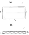
도 3 은 정전 용량형 터치 패널을 구성하는 탑 플레이트의 구조도로서, (A) 는 상기 탑 플레이트의 정면도를 나타내고, (B) 는 그 AA' 선 단면도를 나타내고 있다.
도 4 는 상기 제조 순서의 제 1 공정에 있어서의 탑 플레이트의 형성 과정을 모식적으로 나타내는 단면도이다.
도 5 는 상기 제조 순서의 제 2 공정 내지 제 5 공정에 있어서의 탑 플레이트의 형성 과정을 모식적으로 나타내는 단면도이다.
도 6 은 상기 정전 용량형 터치 패널의 탑 플레이트에 대하여, 실시예와 종래예의 열스트레스 인가 후의 휨의 측정치를 플롯한 그래프이다.
도 7 은 탑 플레이트의 휨 방향을 나타내는 모식도이다.1 is a view showing a structure of a capacitive touch panel according to an embodiment of the present invention. (A) is a front view of the capacitive touch panel, and (B) is a cross-sectional view taken along the line AA 'in (A).
2 is a process diagram showing an example of a manufacturing procedure of the capacitive touch panel.
Fig. 3 is a structural view of a top plate constituting a capacitive touch panel. Fig. 3 (A) is a front view of the top plate, and Fig. 3 (B) is a sectional view taken along the line AA '.
Fig. 4 is a cross-sectional view schematically showing a process of forming a top plate in a first step of the above manufacturing procedure. Fig.
5 is a cross-sectional view schematically showing a process of forming a top plate in a second step to a fifth step of the above manufacturing process.
6 is a graph plotting measured values of warpage after applying heat stress to the top plate of the capacitive touch panel according to the embodiment and the conventional example.
7 is a schematic view showing the bending direction of the top plate.
이하, 본 발명을 실시하기 위한 형태에 대하여 도면을 참조하면서 상세하게 설명한다. 또한, 본 발명은 이하의 실시형태에만 한정되는 것은 아니며, 본 발명의 요지를 일탈하지 않는 범위 내에 있어서 다양한 변경이 가능함은 물론이다. 또한, 도면에 있어서의 각부의 치수는 개략을 나타내는 것으로서, 특히 단면도는 구조를 명료하게 나타내기 위해 두께 방향으로 강조한 치수로 하고 있다.Hereinafter, embodiments for carrying out the present invention will be described in detail with reference to the drawings. It should be noted that the present invention is not limited to the following embodiments, and various modifications may be made without departing from the gist of the present invention. The dimensions of each part in the drawings are schematically shown, and in particular, the cross-sectional views are dimensioned in the thickness direction in order to clearly show the structure.
도 1 은 본 발명에 관련된 정전 용량형 터치 패널 (100) 의 구성예를 나타내는 도면으로, (A) 는 정전 용량형 터치 패널 (100) 의 정면도를 나타내고, (B) 는 그 AA' 선 단면도를 나타내고 있다.1 is a diagram showing a configuration example of a
즉, 본 발명이 적용된 정전 용량형 터치 패널 (100) 은, 상부 구조인 탑 플레이트 (1) 와, 탑 플레이트 (1) 의 배면측에 배치되는 센서부 (10) 를 구성하는 투명 전극층 (8) 및 절연층을 구비한 점퍼 배선층 (12) 을 구비한다.That is, the
탑 플레이트 (1) 는, 도 1 의 (B) 에 나타내는 바와 같이, 내열성이 높은 수지 재료를 포함하는 투명 수지 기재 (2a) 와 그 투명 수지 기재 (2a) 의 일방의 면, 즉 표면에 형성된 경도가 높은 경질 수지 재료를 포함하는 투명 수지층 (2b) 을 구비하는 투명 패널 기판 (2), 투명 수지 기재 (2a) 의 타방의 면, 즉 배면의 외연부에 형성된 가식 인쇄층 (5) 과, 탑 플레이트 (1) 의 배면측 및 가식 인쇄층 (5) 에 걸쳐 덮도록 형성되는 휨방지층 (7) 을 갖는다.As shown in Fig. 1 (B), the
투명 수지 기재 (2a) 는, 내열성이 높은 수지 재료인 PC 수지에 의해 형성되는 것이 바람직하고, 투명 수지층 (2b) 은, 경도가 높은 경질 수지 재료인 PMMA 수지로 형성되는 것이 바람직하다. 일반적으로, 터치 패널 표면의 흠집이 잘 생기지 않는 정도를 연필 경도 (긁기 경도 시험, JIS K 5600) 에 의해 평가하는데, 단일 기재로서의 PC 수지의 표면 경도는 HB ∼ H 로, 흠집이 나기 쉽다. 한편, PMMA 수지의 표면 경도는 3H ∼ 5H 로, 터치 패널의 표면에 사용하는 재료로서 바람직하다. PMMA 수지 등으로 이루어지는 투명 수지층 (2b) 을, PC 수지 등으로 이루어지는 투명 수지 기재 (2a) 의 일방의 면, 즉 정전 용량형 터치 패널 (100) 의 표면측에 형성함으로써, 흠집이 잘 생기지 않는 터치 패널을 실현할 수 있다.The transparent
표면에 투명 수지층 (2b) 이 형성된 투명 수지 기재 (2a) 로 이루어지는 투명 패널 기판 (2) 은, 2 종의 수지 재료를 사용하여, 동시에 용융 성형함으로써 형성된다.The
가식 인쇄층 (5) 은, 스마트 폰이나 태블릿 단말 등을 구성하는 액정 화면의 외연부의 터치 패널을 기능시키는 데에 있어서 필요한 전극이나 배선 등이 형성되어 있는 영역을 액자 영역으로 하여 외부로부터 시인할 수 없도록 덮을 목적으로 형성되는 층이다. 가식 인쇄층 (5) 은, 실크 스크린 인쇄에 의해 유색 잉크를 다층으로 덧칠하여 형성된다. 액자 영역에 형성되어 있는 전극이나 배선 등이 투과되지 않도록 소정의 두께를 도포하기 위해서는, 1 회의 도포로 두껍게 바르는 것은 불균일해지기 쉽기 때문에, 1 회당의 도포층을 얇게 하여 복수회로 나누어 다층의 인쇄층을 형성할 필요가 있다. 예를 들어, 광이 잘 투과되지 않는 진한 색의 잉크인 경우에는, 2 회의 도포에 의해 인쇄층을 형성하고, 광이 투과되기 쉬운 옅은 색 (백색 등) 의 잉크인 경우에는, 4 회 정도의 덧칠을 실시할 필요가 있다. 1 회당의 도포 두께가 8 ㎛ 정도가 되는 경우에는, 옅은 색 잉크의 층은 32 ㎛ 정도의 두께를 갖는다.The
휨방지층 (7) 은, 투명 수지 기재 (2a) 의 배면 및 가식 인쇄층 (5) 에 걸쳐 전면을 덮도록 평탄하게 형성되고, 바람직하게는 투명 수지 기재 (2a) 의 표면측에 형성되는 투명 수지층 (2b) 에 이용되고 있는 재료가 갖는 선팽창 계수와 거의 동등한 선팽창 계수의 수지 재료를 사용한다. 휨방지층 (7) 의 재료로는 특별히 제한은 없고, 자외선 경화형 잉크나 열경화형 잉크에 사용되는 투명의 아크릴계 수지 도료 혹은 우레탄계 수지 도료 등을 사용할 수 있다. 보다 구체적으로는, 우레탄(메트)아크릴레이트, 에폭시(메트)아크릴레이트, 폴리에스테르(메트)아크릴레이트, 폴리에스테르우레탄(메트)아크릴레이트, 폴리에테르(메트)아크릴레이트, 폴리카보네이트(메트)아크릴레이트, 폴리카보네이트우레탄(메트)아크릴레이트 등을 재질로 하는 도료를 사용할 수 있다. 터치 패널의 광학 특성에 영향을 미치지 않도록, 확산 투과광의 전광선 투과광에 대한 비율인 헤이즈가 1 % 를 초과하지 않는 것이 보다 바람직하다. 점도가 낮은 투명의 아크릴계 또는 우레탄계 수지 도료 등을 도포하도록 사용함으로써, 가식 인쇄층 (5) 과 투명 수지 기재 (2a) 사이에 발생하는 단차를 거의 평탄화시켜, 투명 전극층 (8) 을 접속했을 경우에, 이 단차로 인한 배선 끊김을 방지할 수도 있다. 상기 서술한 바와 같이, 옅은 색 잉크로 가식 인쇄를 실시하는 경우에는, 가식 인쇄층 (5) 은 32 ㎛ 정도의 두께가 되므로, 예를 들어 35 ㎛ 정도의 두께가 되도록, 투명 수지 기재 (2a) 의 배면 및 가식 인쇄층 (5) 에 걸쳐 아크릴계 도료를 도포하여 휨방지층 (7) 을 형성하면 된다. 휨방지층 (7) 을 형성하는 아크릴계 도료를 도포하려면, 실크 스크린 인쇄 외에 다이 코터를 사용하여 직접 도포하면 된다. 이와 같이 휨방지층 (7) 의 형성에는, 주지의 도포 기술을 이용할 수 있으므로, 특수한 설비 도입의 필요가 없고, 가식 인쇄층 (5) 의 인쇄 공정에 사용하는 설비와 동일한 것을 사용할 수 있어, 제조 비용의 저감이 가능해진다.The bending
이와 같이, 상기 투명 수지 기재 (2a) 의 배면 및 가식 인쇄층 (5) 에 걸쳐 전면을 덮도록 평탄하게 형성된 상기 휨방지층 (7) 은, 2 종의 수지 재료를 사용하여 형성된 투명 수지층 (2b) 과 투명 수지 기재 (2a) 로 이루어지는 2 층 구조의 투명 패널 기판 (2) 에 생기는 환경 온도에 의한 휨을 방지하기 위한 것이지만, 상기 가식 인쇄층 (5) 과 투명 수지 기재 (2a) 사이에 발생하는 단차를 거의 평탄화시켜, 투명 전극층 (8) 을 접속했을 경우에, 이 단차로 인한 배선 끊김을 방지하는 평탄화층으로서도 기능한다.The bending
휨방지층 (7) 의 하부에 형성되는 투명 전극층 (8) 은, 투명 필름에 투명 전극을 형성한 층으로, 은 또는 구리 혹은 그들의 합금으로 이루어지는 나노 와이어 또는 나노 입자를 포함하는 것으로 할 수 있다. 정전 용량형 터치 패널의 경우에는, 일반적으로는 터치 위치의 xy 좌표를 특정하기 위해서, x 축 방향의 전극 및 y 축 방향의 전극이 2 장의 필름에 형성된 2 층 구조의 투명 전극막을 사용하지만, Ag 나노 와이어를 사용한 투명 전극층 (8) 과 투명 전극의 xy 좌표를 특정하기 위한 점퍼 배선을 다층 형성함으로써 1 층의 투명 전극층 (8) 으로 할 수 있다. 투명 전극층 (8) 을 1 층으로 함으로써, 정전 용량형 터치 패널 (100) 의 두께를 저감시켜 경량화를 도모할 수 있음과 함께, 제조 공정수를 삭감시킬 수 있기 때문에, 제조 비용의 저감이 가능해진다. 또, Ag 나노 와이어막을 사용함으로써, 일반적으로 사용되는 2 장의 ITO 필름에 의한 2 층의 센서 구조를 1 층 구조로 할 수 있고, 두께도 얇게 할 수 있으므로, 새로운 박형화, 경량화에 기여할 수 있다.The
절연층을 구비한 점퍼 배선층 (12) 을 보호하기 위해서, 점퍼 배선층 (12) 의 배면에는, 외부 접속용 플렉시블 프린트 기판 (11) 의 열압착 영역을 제외한 전면을 덮도록 투명 보호막 (9) 이 형성되고, 외부 회로로의 접속을 위한 플렉시블 프린트 기판 (11) 이 접속된다. 투명 보호막 (9) 은, 주지의 재료를 이용하면 되고, 예를 들어 열경화형 아크릴계 수지를 도포함으로써 형성된다.A transparent
이와 같이 본 발명이 적용된 정전 용량형 터치 패널 (100) 에 사용되는 탑 플레이트 (1) 는, 투명 수지 기재 (2a) 와 상기 투명 수지 기재 (2a) 의 일방의 면에 형성된 상이한 재질로 이루어지는 투명 수지층 (2b) 으로 이루어지는 투명 패널 기판 (2) 과, 상기 투명 패널 기판 (2) 의 배면의 외연부에 형성된 가식 인쇄층 (5) 과, 플렉시블 프린트 기판 (11) 의 열압착 온도보다 높은 내열 온도 특성을 갖는 투명 수지 재료로 이루어지고, 상기 가식 인쇄층 (5) 이 형성된 상기 투명 패널 기판 (2) 의 배면에 있어서의 상기 가식 인쇄층 (5) 의 내측 및 그 가식 인쇄층 (5) 의 배면에 걸쳐 덮어 평탄하게 형성된 휨방지층 (7) 과, 상기 휨방지층 (7) 의 배면에 형성된 투명 전극층 (8) 과, 상기 투명 전극층 (8) 상에 형성된 절연층을 구비한 점퍼 배선층 (12) 과, 상기 점퍼 배선층 (12) 상에 형성된 투명 보호막 (9) 을 갖는다.As described above, the
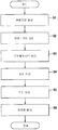
이 정전 용량형 터치 패널 (100) 은, 예를 들어 도 2 의 공정도에 나타내는 순서에 따라 제 1 내지 제 6 공정 (S1 ∼ S6) 의 처리를 실시함으로써 제조된다.The
즉, 제 1 공정 S1 에 있어서, 가식 인쇄층 (5) 이 형성된 가요성을 갖는 투명 패널 기판 (2) 의 배면에 있어서의 상기 가식 인쇄층 (5) 의 단차의 내측 및 그 가식 인쇄층 (5) 의 배면에 휨방지층 (7) 을 형성하고, 제 2 공정 S2 에 있어서, 상기 휨방지층 (7) 의 배면과 평탄 기판 (30) 의 평탄면을 첩합한 상태로 상기 휨방지층 (7) 에 가압 처리를 실시하고, 제 3 공정 S3 에 있어서, 상기 가압 처리를 실시한 상기 휨방지층 (7) 에 추가로 클레이브 처리를 실시하고, 제 4 공정 S4 에 있어서, 상기 클레이브 처리가 실시된 상기 휨방지층 (7) 을 경화시키고, 제 5 공정 S5 에 있어서, 경화시킨 상기 휨방지층 (7) 으로부터 상기 평탄 기판 (30) 을 박리함으로써, 상기 투명 패널 기판 (2), 가식 인쇄층 (5) 및 휨방지층 (7) 으로 이루어지는 도 3 의 (A), (B) 에 나타내는 바와 같은 구조의 탑 플레이트 (1) 를 형성한다. 도 3 의 (A) 는 상기 탑 플레이트 (1) 의 정면도를 나타내고, 도 3 의 (B) 는 그 AA' 선 단면도를 나타내고 있다.That is, in the first step S1, the inner side of the step of the
그리고, 상기 정전 용량형 터치 패널 (100) 은, 제 6 공정 S6 에 있어서, 상기 탑 플레이트 (1) 의 휨방지층 (7) 의 배면에 투명 전극층 (8) 및 절연층을 구비한 점퍼 배선층 (12) 을 구비하는 센서부 (10) 를 형성함으로써 완성된다.The
즉, 먼저 제 1 공정 S1 에 있어서, 외주에 가식 인쇄층 (5) 이 형성된 가요성을 갖는 투명 패널 기판 (2) 의 배면에 있어서의 상기 가식 인쇄층 (5) 의 단차의 내측 및 그 가식 인쇄층 (5) 의 배면에 휨방지층 (7) 을 형성한다.That is, in the first step S1, the inside of the step of the
구체적으로는, 이 제 1 공정 S1 에 있어서, 도 4 의 (A) 에 나타내는 투명 패널 기판 (2) 의 배면 외주 영역에 도 4 의 (B) 에 나타내는 바와 같이 가식 인쇄층 (5) 이 형성된 투명 패널 기판 (2) 에 대하여, 그 투명 패널 기판 (2) 의 배면에 있어서의 상기 가식 인쇄층 (5) 의 단차의 내측 및 그 가식 인쇄층 (5) 의 배면에, 도 4 의 (C) 에 나타내는 바와 같이 자외선 경화 수지를 전면 인쇄 휨방지층 (7) 을 형성함으로써, 상기 투명 패널 기판 (2), 가식 인쇄층 (5) 및 휨방지층 (7) 으로 이루어지는 탑 플레이트 (1) 를 형성한다.Specifically, in this first step S1, as shown in Fig. 4 (B), in the outer peripheral region of the back surface of the
여기서, 가식 인쇄층 (5) 은, 스마트 폰이나 태블릿 단말 등을 구성하는 액정 화면의 외연부에 형성되고, 터치 패널을 기능시키는 데에 있어서 필요한 전극이나 배선 등이 형성되는 영역을 액자 영역으로 하여 외부로부터 시인할 수 없도록 덮을 목적으로 형성되는 층이다. 가식 인쇄층 (5) 은, 예를 들어 실크 스크린 인쇄에 의해 유색 잉크를 다층으로 덧칠하여 형성된다. 액자 영역에 형성되어 있는 전극이나 배선 등이 투과되지 않도록 소정의 두께를 도포하기 위해서는, 1 회의 도포로 두껍게 바르는 것은 불균일해지기 쉽기 때문에, 1 회당의 도포층을 얇게 하여 복수회로 나누어 다층의 인쇄층을 형성할 필요가 있다. 예를 들어, 광이 잘 투과되지 않는 진한 색의 잉크인 경우에는, 2 회의 도포에 의해 인쇄층을 형성하고, 광이 투과되기 쉬운 옅은 색 (백색 등) 의 잉크인 경우에는, 4 회 정도의 덧칠을 실시할 필요가 있다. 1 회당의 도포 두께가 8 ㎛ 정도가 되는 경우에는, 옅은 색 잉크의 층은 32 ㎛ 정도의 두께를 갖는다.Here, the
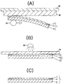
다음의 제 2 공정 S2 에서는, 상기 휨방지층 (7) 의 배면과 평탄 기판 (30) 의 평탄면을 첩합한 상태로 상기 휨방지층 (7) 에 가압 처리를 실시한다.In the next step S2, the bending
구체적으로는, 이 제 2 공정 S2 에서는, 도 5 의 (A) 에 나타내는 바와 같이, 흡인 기능을 구비한 천판 (20) 에 평탄 기판 (30) 으로서 예를 들어 유리 플레이트를 흡착해 두고, 상기 평탄 기판 (30) 과 롤러 (21) 로 상기 탑 플레이트 (1) 를 사이에 두고, 상기 롤러 (21) 를 화살표 방향으로 전동시킴으로써, 상기 평탄 기판 (30) 과 탑 플레이트 (1) 를 첩합하는 첩합 장치를 사용하여, 상기 투명 패널 기판 (2) 측으로부터 상기 휨방지층 (7) 에 상기 롤러 (21) 에 의해 가압 처리를 실시한다.More specifically, in this second step S2, as shown in Fig. 5A, a glass plate, for example, is adsorbed as a
이와 같이, 상기 투명 패널 기판 (2) 측으로부터 상기 휨방지층 (7) 에 상기 롤러 (21) 에 의해 가압 처리를 실시하여 상기 휨방지층 (7) 에 평탄 기판 (30) 을 첩합함으로써, 상기 휨방지층 (7) 의 배면에는 상기 평탄 기판 (30) 의 평탄면이 전사되고, 상기 휨방지층 (7) 의 배면은, 예를 들어 유리 플레이트의 면정밀도, 즉 평탄도나 면조도 등을 갖는 평탄면이 된다. 상기 휨방지층 (7) 은, 가압 처리에 의해 평탄면이 전사된 요철의 최대 높이를 0.1 ㎛ 이하로 한 배면을 갖는 것으로 할 수 있다.As described above, by applying the pressing treatment to the
또, 상기 투명 패널 기판 (2) 측으로부터 상기 휨방지층 (7) 에 상기 롤러 (21) 에 의해 가압 처리를 실시하여 상기 휨방지층 (7) 의 배면에 평탄 기판 (30) 을 첩합할 때에, 상기 롤러 (21) 의 전동 속도를 소정의 일정 속도로 함으로써, 상기 탑 플레이트 (1) 의 가식 인쇄층 (5) 에 의한 단차 부분에 잔존하는 기포를 줄일 수 있다.When the
다음의 제 3 공정 S3 에서는, 상기 가압 처리가 실시된 상기 탑 플레이트 (1) 의 휨방지층 (7) 에 추가로 클레이브 처리를 실시한다.In the following third step S3, the bending
구체적으로는, 이 제 3 공정 S3 에서는, 상기 천판 (20) 에 의한 평탄 기판 (30) 의 흡인을 정지시켜, 상기 탑 플레이트 (1) 를 상기 평탄 기판 (30) 과 함께 상기 천판 (20) 으로부터 이탈시키고, 오토클레이브 압력 가마에 넣고 클레이브 처리를 실시한다.Specifically, in this third step S3, the suction of the
상기 가압 처리가 실시된 상기 탑 플레이트 (1) 의 가식 인쇄층 (5) 에 의한 단차 부분에 잔존하는 기포는, 클레이브 처리를 실시함으로써 더욱 줄일 수 있어, 상기 가식 인쇄층 (5) 의 내측의 화상 표시 영역 내에 잔존하는 기포를 없앨 수 있다.The bubbles remaining in the stepped portion of the
그리고, 다음의 제 4 공정 S4 에서는, 상기 클레이브 처리가 실시된 상기 탑 플레이트 (1) 의 휨방지층 (7) 을 경화시킨다.Then, in the next fourth step S4, the bending
구체적으로는, 이 제 4 공정 S4 에서는, 도 5 의 (B) 에 나타내는 바와 같이, 상기 가압 처리 및 클레이브 처리가 실시된 상기 탑 플레이트 (1) 의 휨방지층 (7) 에 상기 평탄 기판 (30) 측으로부터 자외선 광원 (22) 에 의해 자외선을 조사하여 상기 휨방지층 (7) 을 경화시킨다.Specifically, in this fourth step S4, as shown in Fig. 5B, the
여기서, 상기 평탄 기판 (30) 에는 자외선의 투과율이 높은 투명한 유리 플레이트를 사용함으로써, 상기 평탄 기판 (30) 측으로부터 자외선을 조사하여 상기 휨방지층 (7) 을 효율적으로 경화시킬 수 있다.By using a transparent glass plate having a high transmittance of ultraviolet rays, the
또한, 상기 평탄 기판 (30) 에는, 상기 유리 플레이트 대신에, 예를 들어 이형 처리를 실시한 자외선을 통과시키는 폴리카보네이트 기재 또는 아크릴 수지 기재 등을 사용할 수도 있다.Further, for the
다음의 제 5 공정 S5 에서는, 경화시킨 상기 휨방지층 (7) 으로부터 상기 평탄 기판 (30) 을 박리한다.In the following fifth step S5, the
또한, 상기 평탄 기판 (30) 은, 경화시킨 휨방지층 (7) 으로부터 박리하기 쉽도록, 기판재, 예를 들어 0.5 mm 내지 2 mm 이하의 두께의 유리 플레이트로 이루어지고, 또한 발수제나 박리제를 표면에 도포하는 이형 처리가 실시되어 있는 것으로 하는 것이 바람직하다.The
이와 같이 하여, 상기 제 1 내지 제 5 공정 (S1 ∼ S5) 의 처리에 의해, 도 3 의 (A), (B) 에 나타내는 바와 같은 구조의 탑 플레이트 (1) 가 만들어진다.Thus, the
여기서, 상기 휨방지층 (7) 은, 플렉시블 프린트 기판 (11) 의 열압착 온도보다 높은 내열 온도 특성을 갖는 투명 수지 재료, 예를 들어 경화 후의 내열 온도가 140 ℃ 이상인 아크릴 수지 재료로 이루어지는 것으로 한다.Here, the bending
그리고, 다음의 제 6 공정 S6 에 있어서, 상기 탑 플레이트 (1) 의 휨방지층 (7) 의 배면에 센서부 (10) 를 형성함으로써, 정전 용량형 터치 패널 (100) 을 완성한다.In the next sixth step S6, the
상기 센서부 (10) 는, 절연층을 구비한 점퍼 배선층 (12) 을 보호하기 위해서, 점퍼 배선층 (12) 의 배면에 투명 보호막 (9) 이 형성되고, 외부 회로로의 접속을 위한 플렉시블 프린트 기판 (11) 이 접속된다. 투명 보호막 (9) 은, 주지의 재료를 이용하면 되고, 예를 들어 열경화 혹은 UV 경화형 아크릴계 수지를 도포함으로써 형성된다.The
상기 휨방지층 (7) 또는 투명 보호막 (9) 의 적어도 일방에 미소 수지 비즈를 혼입하여, 0.3 % 이상의 헤이즈를 갖게 한 것으로 할 수 있다.The minute resin beads may be mixed in at least one of the
본 발명이 적용된 정전 용량형 터치 패널 (100) 에 대한 고온 환경하에 있어서의 휨의 발생 상황과, 종래예의 휨의 발생 상황을 측정하였다.The occurrence of bending under the high temperature environment and the occurrence of bending in the conventional example were measured for the
이하에서 작성한 각각의 정전 용량형 터치 패널 시료를, 70 ℃ 로 설정한 열풍식 항온 오븐을 이용하여 240 시간 보존하였다. 그 후, 정전 용량형 터치 패널 시료를 꺼내어, 상온에서 소정의 시간 경과 후에 정전 용량형 터치 패널 시료의 양단에서 휨을 측정하였다. 소정의 시간은, 오븐에서 꺼낸 직후, 5 분 경과 후, 1 시간 경과 후이다.Each capacitive touch panel sample prepared as described below was stored for 240 hours in a hot air oven set at 70 ° C. Thereafter, the capacitance type touch panel sample was taken out, and the warpage was measured at both ends of the capacitance type touch panel sample after lapse of a predetermined time at room temperature. The predetermined time is immediately after taking out of the oven, after 5 minutes, and after 1 hour.
[종래예] 휨의 측정에 사용한 종래예의 정전 용량형 터치 패널 시료[Conventional Example] A conventional capacitive touch panel sample
수지 탑 플레이트 기재 : PC 수지 + PMMA 수지 소재 (MRS58W, 297 mm × 210 mm × 0.8 mm, 미츠비시 가스 화학 제조) Resin Top plate base material: PC resin + PMMA resin material (MRS58W, 297 mm x 210 mm x 0.8 mm, manufactured by Mitsubishi Gas Chemical Co., Ltd.)
가식 인쇄층 : MRX-HF919 흑 (테이코쿠 잉크 제조 제조) Edible printing layer: MRX-HF919 black (manufactured by Teikoku Ink)
광학 접착재 : MHM-FW50 (니치에이 화공 제조) Optical adhesive material: MHM-FW50 (manufactured by Nichia Chemical Co., Ltd.)
ITO-PET : V150A-OFSD5 (닛토 전공 제조)ITO-PET: V150A-OFSD5 (Nitto specialty manufacture)
[실시예 1] 휨의 측정에 사용한 정전 용량형 터치 패널 시료[Example 1] A capacitance type touch panel sample
수지 탑 플레이트 기재 : PC 수지 + PMMA 수지 소재 (MRS58W, 297 mm × 210 mm × 0.8 mm, 미츠비시 가스 화학 제조) Resin Top plate base material: PC resin + PMMA resin material (MRS58W, 297 mm x 210 mm x 0.8 mm, manufactured by Mitsubishi Gas Chemical Co., Ltd.)
가식 인쇄층 : MRX-HF919 흑 (테이코쿠 잉크 제조 제조) Edible printing layer: MRX-HF919 black (manufactured by Teikoku Ink)
휨방지층 : RL-9262 (산유렉 제조) Anti-bending layer: RL-9262 (manufactured by Sanayrec)
투명 전극층 : 은 나노 와이어 잉크 Transparent electrode layer: silver nanowire ink
절연층 : TPAR-P1510PM (토쿄 오카 공업 제조) Insulation layer: TPAR-P1510PM (manufactured by Tokyo Ohka Kogyo Co., Ltd.)
투명 수지 도료 : FR-1TNSD9 (아사히 화학 연구소 제조) Transparent resin: FR-1TNSD9 (manufactured by Asahi Chemical Industry Co., Ltd.)
필러 : 케미스노 MR-3GSN (평균 입경 3 ㎛ : 소켄 화학 제조)Filler: KEMISUNO MR-3GSN (
실시예 1 의 샘플은 다음과 같이 하여 작성하였다.The sample of Example 1 was prepared as follows.
즉, 상기 수지 탑 플레이트 기재 (MRS58W, 297 mm × 210 mm × 0.8 mm, 미츠비시 가스 화학 제조) 에 MRX-HF919 흑 (테이코쿠 잉크 제조 제조) 을 사용하여 실크 스크린 인쇄 (메시 #200) 를 실시하고, 80 ℃ 1 시간 동안 건조·경화시켜, 두께 8 ㎛ 의 가식 인쇄층을 형성하였다. 그 후, 가식 인쇄층 형성부를 포함하는 수지 탑 플레이트 배면 전면에 코로나 처리한 후, 투명 수지 필러 (MR-3GSN) 를 투명 잉크 (RL-9262) 100 중량부에 대하여 0.2 중량부 분산시킨 도료를 사용하고, 그 가식 인쇄층 상에 실크 스크린 인쇄 (메시 #200) 를 실시하여, 가식 인쇄층을 포함하는 수지 탑 플레이트 배면 전면에 휨방지층을 형성하였다. 또한, 이 때의 휨방지층의 두께는 약 12 ㎛ 였다. 그 위에, 은 나노 와이어를 포함하는 도료를 바 코터로 도포하여 제 1 투명 전극층을 형성한 후, 절연층과 점퍼선 (은 나노 와이어) 을 배치하여 제 2 투명 전극층을 형성하였다. 그 후, 투명 수지 도료 (FR-1TNSD9) 를 투명 전극층 전면에 도포하여 투명 보호막을 형성하였다.That is, silk screen printing (mesh # 200) was performed on the resin top plate substrate (MRS58W, 297 mm x 210 mm x 0.8 mm, manufactured by Mitsubishi Gas Chemical Company) using MRX-HF919 black And dried and cured at 80 DEG C for 1 hour to form a decorative print layer having a thickness of 8 mu m. Thereafter, the entire backside of the resin top plate including the decorative print layer forming portion was subjected to corona treatment, and then a paint in which 0.2 weight part of transparent resin filler (MR-3GSN) was dispersed relative to 100 weight parts of transparent ink (RL-9262) , And silk screen printing (mesh # 200) was performed on the decorative printing layer to form a bending prevention layer on the entire rear surface of the resin top plate including the decorative printing layer. The thickness of the bending prevention layer at this time was about 12 占 퐉. A coating material containing silver nanowires was coated thereon with a bar coater to form a first transparent electrode layer, and then an insulating layer and a jumper wire (silver nanowire) were disposed to form a second transparent electrode layer. Thereafter, a transparent resin coating (FR-1TNSD9) was applied to the entire surface of the transparent electrode layer to form a transparent protective film.
그리고, 작성한 정전 용량형 터치 패널 시료를 70 ℃ 의 열풍식 항온 오븐에서 240 시간 보존하고, 꺼냄시의 기재의 휨을 측정하였다.Then, the formed capacitive touch panel sample was stored in a hot-air type thermostat oven at 70 ° C for 240 hours, and the warpage of the substrate at the time of taking out was measured.
그 측정 결과를 도 6 에 나타냄과 함께, 다음의 표 1 에 나타낸다.The measurement results are shown in Fig. 6 and shown in Table 1 below.

도 6 의 그래프의 세로축은 기재의 휨량을 나타내고, 휨의 부호는 도 7 과 같다.The vertical axis in the graph of Fig. 6 represents the amount of warping of the substrate, and the sign of warpage is as shown in Fig.
막대 그래프는 휨의 시간 경과를 나타내고, 보존으로부터 꺼낸 직후, 상온에서 5 분간 방치 후에 측정한 값, 동일하게 1 시간 방치 후에 측정한 값을 적고 있다. 시료는 왼쪽이 종래예에 의한 정전 용량형 터치 패널 시료, 오른쪽이 본 발명에 의한 실시예 1 의 정전 용량형 터치 패널 시료이다.The bar graph shows the elapsed time of warping, and the values measured after leaving for 5 minutes at room temperature immediately after taking out from the storage, and the values measured after 1 hour left in the same manner are written. The left side of the sample is a capacitance type touch panel sample according to the conventional example, and the right side is a capacitance type touch panel sample according to the first embodiment of the present invention.
도 6 에 나타내는 측정 결과로부터 분명한 바와 같이, 특히 꺼냄 직후의 휨에 주목하면, 본 발명에 의한 실시예 1 은 종래예의 약 4 분의 1 의 휨량으로 저감되었다.As is clear from the measurement results shown in Fig. 6, in particular, paying attention to the warp immediately after the take-off, Example 1 of the present invention was reduced to a warp amount of about 1/4 of that of the conventional example.
[실시예 2] 휨방지층의 헤이즈 (흐림도) 와 투명 전극층의 시인성의 측정에 사용한 정전 용량형 터치 패널 시료[Example 2] A capacitive touch panel sample (manufactured by Fuji Photo Film Co., Ltd.) used for measurement of the haze (degree of fogging) of the bending prevention layer and the visibility of the transparent electrode layer
수지 탑 플레이트 기재 : PC 수지 + PMMA 수지 소재 (MRS58W, 297 mm × 210 mm × 0.8 mm, 미츠비시 가스 화학 제조) Resin Top plate base material: PC resin + PMMA resin material (MRS58W, 297 mm x 210 mm x 0.8 mm, manufactured by Mitsubishi Gas Chemical Co., Ltd.)
가식 인쇄층 : MRX-HF919 흑 (테이코쿠 잉크 제조 제조) Edible printing layer: MRX-HF919 black (manufactured by Teikoku Ink)
휨방지층 : RL-9262 (산유렉 제조) Anti-bending layer: RL-9262 (manufactured by Sanayrec)
투명 전극층 : 은 나노 와이어 잉크 Transparent electrode layer: silver nanowire ink
절연층 : TPAR-P1510PM (아사히 화학 연구소 제조) Insulation layer: TPAR-P1510PM (manufactured by Asahi Chemical Industry Co., Ltd.)
투명 수지 필러 : 케미스노 MR-20G (평균 입경 20 ㎛ : 소켄 화학 제조)Transparent resin filler: KEMISUNO MR-20G (average particle size: 20 탆: manufactured by Soken Chemical & Engineering Co., Ltd.)
휨방지층을 형성하는 투명 잉크에 혼입하는 투명 수지 필러를 MR-20G (평균 입경 20 ㎛ ; 소켄 화학) 로 하고, 투명 잉크 100 중량부에 대하여 투명 수지 필러를 10 중량부를 분산시킨 것 이외에는, 실시예 1 과 동등하게 작성하였다.Except that MR-20G (average particle size of 20 mu m; Soken Chemical) was used as a transparent resin filler to be incorporated into the transparent ink forming the bending prevention layer and 10 parts by weight of a transparent resin filler was dispersed in 100 parts by weight of the transparent ink. 1.
[실시예 3] 휨방지층의 헤이즈 (흐림도) 와 투명 전극층의 시인성의 측정에 사용한 정전 용량형 터치 패널 시료[Example 3] A capacitance-type touch panel sample (hereinafter referred to as " transparent electrode layer ") used for measurement of the haze
수지 탑 플레이트 기재 : PC 수지 + PMMA 수지 소재 (MRS58W, 297 mm × 210 mm × 0.8 mm, 미츠비시 가스 화학 제조) Resin Top plate base material: PC resin + PMMA resin material (MRS58W, 297 mm x 210 mm x 0.8 mm, manufactured by Mitsubishi Gas Chemical Co., Ltd.)
가식 인쇄층 : MRX-HF919 흑 (테이코쿠 잉크 제조 제조) Edible printing layer: MRX-HF919 black (manufactured by Teikoku Ink)
휨방지층 : RL-9262 (산유렉 제조) Anti-bending layer: RL-9262 (manufactured by Sanayrec)
투명 전극층 : 은 나노 와이어 잉크 Transparent electrode layer: silver nanowire ink
절연층 : TPAR-P1510PM (아사히 화학 연구소 제조) Insulation layer: TPAR-P1510PM (manufactured by Asahi Chemical Industry Co., Ltd.)
투명 수지 필러 : 케미스노 MR-10G (평균 입경 9 ㎛ : 소켄 화학 제조)Transparent resin filler: KEMISUNO MR-10G (average particle size: 9 mu m, manufactured by Soeken Chemical Co., Ltd.)
휨방지층을 형성하는 투명 잉크에 혼입하는 투명 수지 필러를 MR-10G (평균 입경 9 ㎛ ; 소켄 화학) 로 하고, 투명 잉크 100 중량부에 대하여 투명 수지 필러를 1 중량부를 분산시킨 것 이외에는, 실시예 1 과 동등하게 작성하였다.Except that the transparent resin filler to be incorporated into the transparent ink forming the bending preventive layer was MR-10G (average particle size: 9 mu m; Socene Chemical), and 1 part by weight of the transparent resin filler was dispersed in 100 parts by weight of the transparent ink. 1.
[비교예] 휨방지층의 헤이즈 (흐림도) 와 투명 전극층의 시인성의 측정에 사용한 정전 용량형 터치 패널 시료[Comparative Example] A capacitive touch panel sample (hereinafter referred to as " capacitive touch panel sample ") used for measurement of the haze
수지 탑 플레이트 기재 : PC 수지 + PMMA 수지 소재 (MRS58W, 297 mm × 210 mm × 0.8 mm, 미츠비시 가스 화학 제조) Resin Top plate base material: PC resin + PMMA resin material (MRS58W, 297 mm x 210 mm x 0.8 mm, manufactured by Mitsubishi Gas Chemical Co., Ltd.)
가식 인쇄층 : MRX-HF919 흑 (테이코쿠 잉크 제조 제조) Edible printing layer: MRX-HF919 black (manufactured by Teikoku Ink)
휨방지층 : RL-9262 (산유렉 제조) Anti-bending layer: RL-9262 (manufactured by Sanayrec)
투명 전극층 : 은 나노 와이어 잉크 Transparent electrode layer: silver nanowire ink
절연층 : TPAR-P1510PM (아사히 화학 연구소 제조)Insulation layer: TPAR-P1510PM (manufactured by Asahi Chemical Industry Co., Ltd.)
휨방지층을 형성하는 투명 잉크에는, 투명 수지 필러 등을 혼입하지 않은 것 이외에는, 실시예 1 과 동등하게 작성하였다.The transparent ink forming the bending prevention layer was formed in the same manner as in Example 1 except that no transparent resin filler or the like was mixed.
상기 실시예 1 ∼ 3 및 비교예에 대하여 휨방지층의 헤이즈 (흐림도) 와 투명 전극층의 시인성을 관측한 결과를 다음의 표 2 에 나타낸다.Table 2 shows the results of observing the haze (fogging degree) of the bending prevention layer and the visibility of the transparent electrode layer in Examples 1 to 3 and Comparative Examples.

투명 전극층은 은 나노 와이어 잉크로 형성되어 있고, 은 나노 와이어가 존재하는 전극 부분과 동 존재하지 않는 절연 부분에서는, 수지 탑 플레이트 표면으로부터의 입사광에 대한 반사율이 상이하다. 그러므로 전극 부분이 시인되어 버린다. 실시예 1 ∼ 3 과 같이, 휨방지층의 헤이즈가 0.3 % 이상인 경우, 그 위에 형성되는 투명 전극층이 시인되지 않는 것을 알 수 있었다.The transparent electrode layer is formed of silver nanowire ink, and the reflectance of incident light from the surface of the resin top plate is different in an insulating portion that is not coexistent with the electrode portion in which silver nanowires exist. Therefore, the electrode portion is visible. As in Examples 1 to 3, when the haze of the bending prevention layer was 0.3% or more, it was found that the transparent electrode layer formed thereon was not visually observed.
또, 외부 접속용 기판, 즉 플렉시블 프린트 기판 (Flexible Printed Circuits ; 이하, FPC) (11) 을 열압착했을 때의, 압착 지그에 의한 기재의 열변형에 대하여, 그 압착흔의 시인성을 관측한 결과를 다음의 표 3 에 나타낸다.In addition, when the substrate for external connection, that is, the flexible printed circuit (Flexible Printed Circuits: hereinafter referred to as FPC) 11, was thermally bonded, the thermal deformation of the substrate by the compression bonding jig Are shown in Table 3 below.

압착 지그의 온도는 150 ℃, 압력은 약 4 ㎫, 압착 시간은 10 초이다. 비교예로서, 하기 기재를 이용하고, 휨방지층이 없는 것 이외에는 실시예 1 과 동일한 구성으로 터치 패널을 작성하였다.The temperature of the compression jig is 150 DEG C, the pressure is about 4 MPa, and the compression time is 10 seconds. As a comparative example, the following substrate was used and a touch panel was made with the same constitution as that of Example 1 except that no bending prevention layer was provided.
PMMA : 단층 기재 (품명 : CLAREX 1.0 mm 닛토 수지 공업 제조) PMMA: single-layer substrate (trade name: CLAREX 1.0 mm, manufactured by Nitto Resin Co., Ltd.)
PMMA/PC/PMMA : 2 종 3 층 기재 (품명 : 하츠라스 HI-HAIV 0.8 mm 후쿠비 화학 공업 제조)PMMA / PC / PMMA: two kinds of three-layer substrate (name: Hatsuras HI-HAIV 0.8 mm manufactured by Fukubi Chemical Industry Co., Ltd.)
FPC 의 열압착 지그가 접촉하는 부분은, 실시예 1 에서는 휨방지층 (UV 경화성 아크릴 수지), 비교예의 PMMA (단층) 와, PMMA/PC/PMMA (2 종 3 층) 에서는 PMMA 수지층이다. 이들 접촉하는 부분의 내열성이 열변형 정도에 영향을 미친다.The contact portion of the FPC with the thermocompression jig is a bending prevention layer (UV curable acrylic resin) in Example 1, a PMMA (monolayer) in a comparative example, and a PMMA resin layer in a PMMA / PC / PMMA (two kinds of three layers). The heat resistance of these contacting portions affects the degree of thermal deformation.
표 3 의 결과에서도 분명한 바와 같이, 실시예 1 의 휨방지층은 충분한 내열성이 있으므로, FPC 의 압착부의 변형이 없어 압착흔을 수지 탑 플레이트 표면으로부터 시인할 수 없다. 따라서, 본 발명은 터치 패널로서 양호한 수지 탑 플레이트를 제공할 수 있다.As is evident from the results in Table 3, the bending prevention layer of Example 1 has sufficient heat resistance, so that there is no deformation of the pressed portion of the FPC, so that the pressing marks can not be seen from the surface of the resin top plate. Therefore, the present invention can provide a good resin top plate as a touch panel.
1 : 탑 플레이트
2a : 투명 수지 기재
2b : 투명 수지층
2 : 투명 패널 기판
5 : 가식 인쇄층
7 : 휨방지층
8 : 투명 전극층
9 : 투명 보호막
10 : 센서부
100 : 정전 용량형 터치 패널
11 : 플렉시블 프린트 기판
12 : 절연층을 구비한 점퍼 배선층 1: Top plate
2a: transparent resin substrate
2b: transparent resin layer
2: transparent panel substrate
5: embossed printing layer
7:
8: transparent electrode layer
9: Transparent protective film
10: Sensor unit
100: Capacitive touch panel
11: Flexible printed circuit board
12: jumper wiring layer with insulating layer
Claims (5)
상기 투명 패널 기판의 배면의 외연부에 형성된 가식 인쇄층과,
외부 접속용 기판의 열압착 온도보다 높은 내열 온도 특성을 갖는 투명 수지 재료로 이루어지고, 상기 가식 인쇄층이 형성된 상기 투명 패널 기판의 배면에 있어서의 상기 가식 인쇄층의 내측 및 그 가식 인쇄층의 배면에 걸쳐 덮어 평탄하게 형성된 휨방지층과,
상기 휨방지층의 배면에 형성된 투명 전극층과,
상기 투명 전극층의 배면에 형성된 절연층을 구비한 점퍼 배선층과,
상기 점퍼 배선층의 배면에 상기 외부 접속용 기판의 열압착 영역을 제외한 전면을 덮도록 형성된 투명 보호막을 갖는 것을 특징으로 하는 정전 용량형 터치 패널.A transparent panel substrate comprising a transparent resin substrate and a transparent resin layer made of a different material formed on one surface of the transparent resin substrate,
An edible print layer formed on the outer edge of the back surface of the transparent panel substrate,
Wherein the transparent printed circuit board is made of a transparent resin material having a heat-resistant temperature characteristic higher than a thermal compression temperature of the substrate for external connection, and the inside of the edible printed layer on the back surface of the transparent panel substrate on which the edible printed layer is formed, A bending prevention layer formed to cover the surface of the substrate,
A transparent electrode layer formed on the back surface of the bending prevention layer,
A jumper wiring layer having an insulating layer formed on a back surface of the transparent electrode layer,
And a transparent protective film formed on a rear surface of the jumper wiring layer so as to cover a front surface of the substrate for external connection excluding a thermocompression region.
상기 휨방지층은, 경화 후의 내열 온도가 140 ℃ 이상인 아크릴 수지 재료로 이루어지는 것을 특징으로 하는 정전 용량형 터치 패널.The method according to claim 1,
Wherein the bending prevention layer is made of an acrylic resin material having a heat resistance temperature after curing of 140 占 폚 or higher.
상기 투명 전극층은, 은 또는 구리 혹은 그들의 합금으로 이루어지는 나노 와이어 또는 나노 입자를 포함하는 것을 특징으로 하는 정전 용량형 터치 패널.The method according to claim 1,
Wherein the transparent electrode layer comprises nanowires or nanoparticles made of silver, copper, or an alloy thereof.
상기 휨방지층 또는 상기 투명 보호막의 적어도 일방에 미소 수지 비즈를 혼입하여, 0.3 % 이상의 헤이즈를 갖게 한 것을 특징으로 하는 정전 용량형 터치 패널.The method according to claim 1,
Wherein at least one of the bending prevention layer or the transparent protective film is mixed with minute resin beads to have a haze of 0.3% or more.
상기 휨방지층은, 가압 처리에 의해 평탄면이 전사된 요철의 최대 높이를 0.1 ㎛ 이하로 한 배면을 갖는 것을 특징으로 하는 정전 용량형 터치 패널.The method according to claim 1,
Wherein the bending prevention layer has a back surface with a maximum height of the concavities and convexities to which the flat surface is transferred by the pressing treatment to 0.1 占 퐉 or less.
Applications Claiming Priority (3)
| Application Number | Priority Date | Filing Date | Title |
|---|---|---|---|
| JP2013185530A JP5848736B2 (en) | 2013-09-06 | 2013-09-06 | Capacitive touch panel |
| JPJP-P-2013-185530 | 2013-09-06 | ||
| PCT/JP2014/004562 WO2015033569A1 (en) | 2013-09-06 | 2014-09-04 | Capacitive touch panel |
Publications (1)
| Publication Number | Publication Date |
|---|---|
| KR20160053923A true KR20160053923A (en) | 2016-05-13 |
Family
ID=52628065
Family Applications (1)
| Application Number | Title | Priority Date | Filing Date |
|---|---|---|---|
| KR1020167005768A KR20160053923A (en) | 2013-09-06 | 2014-09-04 | Capacitive touch panel |
Country Status (7)
| Country | Link |
|---|---|
| US (1) | US20160202801A1 (en) |
| EP (1) | EP3043242A4 (en) |
| JP (1) | JP5848736B2 (en) |
| KR (1) | KR20160053923A (en) |
| CN (1) | CN105518592A (en) |
| TW (1) | TW201523377A (en) |
| WO (1) | WO2015033569A1 (en) |
Families Citing this family (8)
| Publication number | Priority date | Publication date | Assignee | Title |
|---|---|---|---|---|
| JP2016173736A (en) * | 2015-03-17 | 2016-09-29 | アルプス電気株式会社 | Sensor panel and manufacturing method therefor |
| CN104994318A (en) * | 2015-07-28 | 2015-10-21 | 张家港保税区佰昂特种玻璃有限公司 | Thermo-sensitive television touch screen |
| KR20170018718A (en) * | 2015-08-10 | 2017-02-20 | 삼성전자주식회사 | Transparent electrode using amorphous alloy and method for manufacturing the same |
| JP6554365B2 (en) * | 2015-09-04 | 2019-07-31 | アルプスアルパイン株式会社 | Manufacturing method of exterior panel |
| KR102512276B1 (en) * | 2016-03-07 | 2023-03-22 | 삼성디스플레이 주식회사 | Bonding apparatus and bonding method using the same |
| CN106020554A (en) * | 2016-06-06 | 2016-10-12 | 京东方科技集团股份有限公司 | Tough cover plate, manufacturing method thereof and touch display device |
| KR20240012622A (en) | 2016-12-07 | 2024-01-29 | 플라트프로그 라보라토리즈 에이비 | An improved touch device |
| EP4104042A1 (en) | 2020-02-10 | 2022-12-21 | FlatFrog Laboratories AB | Improved touch-sensing apparatus |
Family Cites Families (12)
| Publication number | Priority date | Publication date | Assignee | Title |
|---|---|---|---|---|
| JP4435890B2 (en) | 1999-01-12 | 2010-03-24 | 日本写真印刷株式会社 | Touch panel |
| JP2003045234A (en) * | 2001-07-26 | 2003-02-14 | Dainippon Printing Co Ltd | Transparent conductive film |
| WO2006041089A1 (en) * | 2004-10-15 | 2006-04-20 | Mitsubishi Rayon Co., Ltd. | Active energy beam curing resin composition and sheet-form optical article |
| US8363201B2 (en) * | 2007-01-18 | 2013-01-29 | Arizona Board Of Regents, A Body Corporate Of The State Of Arizona Acting For And On Behalf Of Arizona State University | Flexible transparent electrodes via nanowires and sacrificial conductive layer |
| TWM348999U (en) | 2008-02-18 | 2009-01-11 | Tpk Touch Solutions Inc | Capacitive touch panel |
| JP2012125991A (en) * | 2010-12-15 | 2012-07-05 | Nitto Denko Corp | Laminate |
| JP2012209030A (en) * | 2011-03-29 | 2012-10-25 | Toray Advanced Film Co Ltd | Transparent conductive laminate and method for manufacturing the same |
| JP5651526B2 (en) * | 2011-04-28 | 2015-01-14 | 藤森工業株式会社 | Hard coat film and touch panel using the same |
| CN102929454A (en) * | 2011-08-12 | 2013-02-13 | 宸鸿科技(厦门)有限公司 | Capacitive touch panel and method for reducing visibility of metal conductors thereof |
| JP2013127546A (en) * | 2011-12-19 | 2013-06-27 | Panasonic Corp | Anti-reflection film with transparent electrodes |
| JP5671485B2 (en) * | 2012-01-11 | 2015-02-18 | 綜研化学株式会社 | Adhesive tape for conductive film and laminate for touch panel |
| US20140362309A1 (en) * | 2012-01-25 | 2014-12-11 | Kyocera Corporation | Input device, display device, and electronic equipment |
-
2013
- 2013-09-06 JP JP2013185530A patent/JP5848736B2/en active Active
-
2014
- 2014-09-04 US US14/915,960 patent/US20160202801A1/en not_active Abandoned
- 2014-09-04 WO PCT/JP2014/004562 patent/WO2015033569A1/en active Application Filing
- 2014-09-04 CN CN201480048807.0A patent/CN105518592A/en active Pending
- 2014-09-04 KR KR1020167005768A patent/KR20160053923A/en not_active Application Discontinuation
- 2014-09-04 EP EP14841568.0A patent/EP3043242A4/en not_active Withdrawn
- 2014-09-05 TW TW103130779A patent/TW201523377A/en unknown
Also Published As
| Publication number | Publication date |
|---|---|
| WO2015033569A1 (en) | 2015-03-12 |
| JP2015052916A (en) | 2015-03-19 |
| CN105518592A (en) | 2016-04-20 |
| EP3043242A4 (en) | 2017-05-10 |
| EP3043242A1 (en) | 2016-07-13 |
| TW201523377A (en) | 2015-06-16 |
| JP5848736B2 (en) | 2016-01-27 |
| US20160202801A1 (en) | 2016-07-14 |
Similar Documents
| Publication | Publication Date | Title |
|---|---|---|
| KR20160053923A (en) | Capacitive touch panel | |
| KR101288198B1 (en) | Input apparatus and method for manufacturing the same | |
| WO2015045325A1 (en) | Capacitive curved touch panel and method for fabrication thereof | |
| KR102373615B1 (en) | Display device having window member and fabricating mathod for window member | |
| WO2015025710A1 (en) | Capacitive touch panel and method for manufacturing same | |
| KR102389697B1 (en) | Curved Tempered Glass, Curved Tempered Glass Film And Method For Manufacturing The Same | |
| TW201539279A (en) | Laminate, method for producing laminate, capacitive touch panel and image display device | |
| JP2015530942A (en) | Laminated body including pressure-sensitive adhesive layer and method for producing the same | |
| JP2017062430A (en) | Adhesive laminate and manufacturing method of the same | |
| JP5795357B2 (en) | Capacitive touch panel | |
| JP5860837B2 (en) | Capacitive touch panel | |
| WO2017138364A1 (en) | Liquid crystal display device | |
| KR20140051055A (en) | Surface panel with detection function and method for manufacturing thereof | |
| TW201537430A (en) | Laminate, method for producing laminate, capacitive touch panel and image display device | |
| JP5856114B2 (en) | Manufacturing method of capacitive touch panel | |
| JP2015095022A (en) | Electrostatic capacitance touch panel |
Legal Events
| Date | Code | Title | Description |
|---|---|---|---|
| WITN | Application deemed withdrawn, e.g. because no request for examination was filed or no examination fee was paid |