KR20160048314A - Dc-dc converter and display apparatus having the same - Google Patents
Dc-dc converter and display apparatus having the same Download PDFInfo
- Publication number
- KR20160048314A KR20160048314A KR1020140144511A KR20140144511A KR20160048314A KR 20160048314 A KR20160048314 A KR 20160048314A KR 1020140144511 A KR1020140144511 A KR 1020140144511A KR 20140144511 A KR20140144511 A KR 20140144511A KR 20160048314 A KR20160048314 A KR 20160048314A
- Authority
- KR
- South Korea
- Prior art keywords
- voltage
- switch
- slew rate
- level
- turned
- Prior art date
Links
Images


Classifications
-
- G—PHYSICS
- G09—EDUCATION; CRYPTOGRAPHY; DISPLAY; ADVERTISING; SEALS
- G09G—ARRANGEMENTS OR CIRCUITS FOR CONTROL OF INDICATING DEVICES USING STATIC MEANS TO PRESENT VARIABLE INFORMATION
- G09G5/00—Control arrangements or circuits for visual indicators common to cathode-ray tube indicators and other visual indicators
-
- G—PHYSICS
- G09—EDUCATION; CRYPTOGRAPHY; DISPLAY; ADVERTISING; SEALS
- G09G—ARRANGEMENTS OR CIRCUITS FOR CONTROL OF INDICATING DEVICES USING STATIC MEANS TO PRESENT VARIABLE INFORMATION
- G09G3/00—Control arrangements or circuits, of interest only in connection with visual indicators other than cathode-ray tubes
- G09G3/20—Control arrangements or circuits, of interest only in connection with visual indicators other than cathode-ray tubes for presentation of an assembly of a number of characters, e.g. a page, by composing the assembly by combination of individual elements arranged in a matrix no fixed position being assigned to or needed to be assigned to the individual characters or partial characters
- G09G3/34—Control arrangements or circuits, of interest only in connection with visual indicators other than cathode-ray tubes for presentation of an assembly of a number of characters, e.g. a page, by composing the assembly by combination of individual elements arranged in a matrix no fixed position being assigned to or needed to be assigned to the individual characters or partial characters by control of light from an independent source
- G09G3/36—Control arrangements or circuits, of interest only in connection with visual indicators other than cathode-ray tubes for presentation of an assembly of a number of characters, e.g. a page, by composing the assembly by combination of individual elements arranged in a matrix no fixed position being assigned to or needed to be assigned to the individual characters or partial characters by control of light from an independent source using liquid crystals
- G09G3/3611—Control of matrices with row and column drivers
- G09G3/3696—Generation of voltages supplied to electrode drivers
-
- H—ELECTRICITY
- H02—GENERATION; CONVERSION OR DISTRIBUTION OF ELECTRIC POWER
- H02M—APPARATUS FOR CONVERSION BETWEEN AC AND AC, BETWEEN AC AND DC, OR BETWEEN DC AND DC, AND FOR USE WITH MAINS OR SIMILAR POWER SUPPLY SYSTEMS; CONVERSION OF DC OR AC INPUT POWER INTO SURGE OUTPUT POWER; CONTROL OR REGULATION THEREOF
- H02M1/00—Details of apparatus for conversion
- H02M1/08—Circuits specially adapted for the generation of control voltages for semiconductor devices incorporated in static converters
-
- H—ELECTRICITY
- H02—GENERATION; CONVERSION OR DISTRIBUTION OF ELECTRIC POWER
- H02M—APPARATUS FOR CONVERSION BETWEEN AC AND AC, BETWEEN AC AND DC, OR BETWEEN DC AND DC, AND FOR USE WITH MAINS OR SIMILAR POWER SUPPLY SYSTEMS; CONVERSION OF DC OR AC INPUT POWER INTO SURGE OUTPUT POWER; CONTROL OR REGULATION THEREOF
- H02M3/00—Conversion of dc power input into dc power output
- H02M3/02—Conversion of dc power input into dc power output without intermediate conversion into ac
- H02M3/04—Conversion of dc power input into dc power output without intermediate conversion into ac by static converters
- H02M3/10—Conversion of dc power input into dc power output without intermediate conversion into ac by static converters using discharge tubes with control electrode or semiconductor devices with control electrode
- H02M3/145—Conversion of dc power input into dc power output without intermediate conversion into ac by static converters using discharge tubes with control electrode or semiconductor devices with control electrode using devices of a triode or transistor type requiring continuous application of a control signal
- H02M3/155—Conversion of dc power input into dc power output without intermediate conversion into ac by static converters using discharge tubes with control electrode or semiconductor devices with control electrode using devices of a triode or transistor type requiring continuous application of a control signal using semiconductor devices only
- H02M3/156—Conversion of dc power input into dc power output without intermediate conversion into ac by static converters using discharge tubes with control electrode or semiconductor devices with control electrode using devices of a triode or transistor type requiring continuous application of a control signal using semiconductor devices only with automatic control of output voltage or current, e.g. switching regulators
-
- H—ELECTRICITY
- H03—ELECTRONIC CIRCUITRY
- H03K—PULSE TECHNIQUE
- H03K17/00—Electronic switching or gating, i.e. not by contact-making and –breaking
- H03K17/16—Modifications for eliminating interference voltages or currents
- H03K17/161—Modifications for eliminating interference voltages or currents in field-effect transistor switches
-
- G—PHYSICS
- G09—EDUCATION; CRYPTOGRAPHY; DISPLAY; ADVERTISING; SEALS
- G09G—ARRANGEMENTS OR CIRCUITS FOR CONTROL OF INDICATING DEVICES USING STATIC MEANS TO PRESENT VARIABLE INFORMATION
- G09G2310/00—Command of the display device
- G09G2310/06—Details of flat display driving waveforms
- G09G2310/066—Waveforms comprising a gently increasing or decreasing portion, e.g. ramp
-
- G—PHYSICS
- G09—EDUCATION; CRYPTOGRAPHY; DISPLAY; ADVERTISING; SEALS
- G09G—ARRANGEMENTS OR CIRCUITS FOR CONTROL OF INDICATING DEVICES USING STATIC MEANS TO PRESENT VARIABLE INFORMATION
- G09G2310/00—Command of the display device
- G09G2310/06—Details of flat display driving waveforms
- G09G2310/067—Special waveforms for scanning, where no circuit details of the gate driver are given
-
- G—PHYSICS
- G09—EDUCATION; CRYPTOGRAPHY; DISPLAY; ADVERTISING; SEALS
- G09G—ARRANGEMENTS OR CIRCUITS FOR CONTROL OF INDICATING DEVICES USING STATIC MEANS TO PRESENT VARIABLE INFORMATION
- G09G2310/00—Command of the display device
- G09G2310/08—Details of timing specific for flat panels, other than clock recovery
-
- G—PHYSICS
- G09—EDUCATION; CRYPTOGRAPHY; DISPLAY; ADVERTISING; SEALS
- G09G—ARRANGEMENTS OR CIRCUITS FOR CONTROL OF INDICATING DEVICES USING STATIC MEANS TO PRESENT VARIABLE INFORMATION
- G09G2330/00—Aspects of power supply; Aspects of display protection and defect management
- G09G2330/02—Details of power systems and of start or stop of display operation
- G09G2330/021—Power management, e.g. power saving
-
- G—PHYSICS
- G09—EDUCATION; CRYPTOGRAPHY; DISPLAY; ADVERTISING; SEALS
- G09G—ARRANGEMENTS OR CIRCUITS FOR CONTROL OF INDICATING DEVICES USING STATIC MEANS TO PRESENT VARIABLE INFORMATION
- G09G2330/00—Aspects of power supply; Aspects of display protection and defect management
- G09G2330/02—Details of power systems and of start or stop of display operation
- G09G2330/028—Generation of voltages supplied to electrode drivers in a matrix display other than LCD
-
- G—PHYSICS
- G09—EDUCATION; CRYPTOGRAPHY; DISPLAY; ADVERTISING; SEALS
- G09G—ARRANGEMENTS OR CIRCUITS FOR CONTROL OF INDICATING DEVICES USING STATIC MEANS TO PRESENT VARIABLE INFORMATION
- G09G2330/00—Aspects of power supply; Aspects of display protection and defect management
- G09G2330/06—Handling electromagnetic interferences [EMI], covering emitted as well as received electromagnetic radiation
-
- G—PHYSICS
- G09—EDUCATION; CRYPTOGRAPHY; DISPLAY; ADVERTISING; SEALS
- G09G—ARRANGEMENTS OR CIRCUITS FOR CONTROL OF INDICATING DEVICES USING STATIC MEANS TO PRESENT VARIABLE INFORMATION
- G09G3/00—Control arrangements or circuits, of interest only in connection with visual indicators other than cathode-ray tubes
- G09G3/20—Control arrangements or circuits, of interest only in connection with visual indicators other than cathode-ray tubes for presentation of an assembly of a number of characters, e.g. a page, by composing the assembly by combination of individual elements arranged in a matrix no fixed position being assigned to or needed to be assigned to the individual characters or partial characters
-
- H—ELECTRICITY
- H02—GENERATION; CONVERSION OR DISTRIBUTION OF ELECTRIC POWER
- H02M—APPARATUS FOR CONVERSION BETWEEN AC AND AC, BETWEEN AC AND DC, OR BETWEEN DC AND DC, AND FOR USE WITH MAINS OR SIMILAR POWER SUPPLY SYSTEMS; CONVERSION OF DC OR AC INPUT POWER INTO SURGE OUTPUT POWER; CONTROL OR REGULATION THEREOF
- H02M1/00—Details of apparatus for conversion
- H02M1/0003—Details of control, feedback or regulation circuits
- H02M1/0029—Circuits or arrangements for limiting the slope of switching signals, e.g. slew rate
Abstract
Description
본 발명은 DC-DC 컨버터 및 이를 포함하는 표시 장치에 관한 것으로, 보다 상세하게는 노이즈를 감소시킬 수 있는 DC-DC 컨버터 및 이를 포함하는 표시 장치에 관한 것이다.BACKGROUND OF THE
DC-DC 컨버터 및 이를 포함하는 전자 장치의 브로드 밴드 파워 노이즈는 주로 상기 DC-DC 컨버터 내의 스위칭부의 턴 온 및 턴 오프 시에 발생하는 라이징 노이즈 및 폴링 노이즈에 기인한다. The broadband power noise of a DC-DC converter and an electronic device including the DC-DC converter is mainly caused by rising noise and polling noise generated when the switching unit is turned on and off in the DC-DC converter.
상기 스위칭부의 양 단에 저항 및 캐패시터가 직렬로 연결된 스너버(Snubber) 회로를 연결하는 경우, 상기 스위칭부의 턴 온 및 턴 오프 시에 발생하는 링 파형의 크기를 줄일 수 있다. When a snubber circuit, in which a resistor and a capacitor are connected in series, is connected to both ends of the switching unit, the size of the ring waveform generated when the switching unit is turned on and off can be reduced.
그러나, 상기 스너버 회로를 연결할 경우, 부품 수 증가, 상기 저항으로 인한 효율의 저하 및 발명 등의 문제가 발생할 수 있다. However, when the snubber circuit is connected, problems such as an increase in the number of parts, a decrease in efficiency due to the resistance, and the like may occur.
이에 본 발명의 기술적 과제는 이러한 점에서 착안된 것으로, 본 발명의 목적은 노이즈를 감소시킬 수 있는 DC-DC 컨버터를 제공하는 것이다.Accordingly, it is an object of the present invention to provide a DC-DC converter capable of reducing noise.
본 발명의 다른 목적은 상기 DC-DC 컨버터를 포함하는 표시 장치를 제공하는 것이다.Another object of the present invention is to provide a display device including the DC-DC converter.
상기한 본 발명의 목적을 실현하기 위한 일 실시예에 따른 DC-DC 컨버터는 파워 스위치 및 스위칭 컨트롤러를 포함한다. 상기 파워 스위치는 턴 온 및 턴 오프를 반복하여 입력 DC 전압을 기초로 출력 DC 전압을 생성한다. 상기 스위칭 컨트롤러는 상기 파워 스위치의 동작을 제어한다. 상기 스위칭 컨트롤러는 상기 파워 스위치의 일단의 스위치 전압의 슬루율을 시간에 따라 가변시키는 슬루율 제어부를 포함한다.The DC-DC converter according to an embodiment for realizing the object of the present invention includes a power switch and a switching controller. The power switch repeats turn-on and turn-off to produce an output DC voltage based on the input DC voltage. The switching controller controls the operation of the power switch. The switching controller includes a slew rate control unit for varying a slew rate of a switch voltage at one end of the power switch according to time.
본 발명의 일 실시예에 있어서, 상기 스위칭 컨트롤러는 제1 주기를 갖는 제1 전압의 레벨을 조절하여 상기 제1 주기를 갖는 제2 전압을 생성하는 스위치 게이트 구동부를 더 포함할 수 있다. According to an embodiment of the present invention, the switching controller may further include a switch gate driver for adjusting a level of a first voltage having a first period to generate a second voltage having the first period.
본 발명의 일 실시예에 있어서, 상기 슬루율 제어부는 병렬로 연결되는 N개의 저항들을 포함할 수 있다. 상기 N개의 저항들은 상기 N개의 저항들에 직렬로 연결되는 N개의 스위치들에 의해 상기 파워 스위치와 상기 스위치 게이트 구동부를 교대로 연결할 수 있다. In one embodiment of the present invention, the slew rate control unit may include N resistors connected in parallel. The N resistors may alternately connect the power switch and the switch gate driver by N switches serially connected to the N resistors.
본 발명의 일 실시예에 있어서, 상기 N개의 저항들은 서로 다른 저항 값을 가질 수 있다. In one embodiment of the present invention, the N resistors may have different resistance values.
본 발명의 일 실시예에 있어서, 상기 파워 스위치와 상기 스위치 게이트 구동부를 연결하는 상기 슬루율 제어부의 저항 값이 클수록 상기 스위치 전압의 슬루율이 낮아질 수 있다. In one embodiment of the present invention, the higher the resistance value of the slew rate control unit that connects the power switch and the switch gate driver, the lower the slew rate of the switch voltage.
본 발명의 일 실시예에 있어서, 상기 슬루율 제어부의 제1 스위치 내지 제N 스위치는 순차적으로 턴 온 될 수 있다. 상기 제N 스위치가 턴 온 된 후 상기 제1 스위치가 턴 온 될 수 있다. 상기 제1 스위치가 턴 온 되고, 다시 상기 제1 스위치가 턴 온 될 때까지의 시간으로 정의되는 슬루율 변화 주기는 상기 제1 주기의 N배일 수 있다. In one embodiment of the present invention, the first switch to the Nth switch of the slew rate control unit may be sequentially turned on. After the Nth switch is turned on, the first switch may be turned on. The slew rate change period defined by the time until the first switch is turned on and the first switch is turned on may be N times the first period.
본 발명의 일 실시예에 있어서, 상기 슬루율 제어부의 제1 스위치 내지 제N 스위치는 순차적으로 턴 온 될 수 있다. 상기 제N 스위치가 턴 온 된 후 제N-1 스위치 내지 상기 제1 스위치가 순차적으로 턴 온 될 수 있다. 상기 제1 스위치가 턴 온 되고, 다시 상기 제1 스위치가 턴 온 될 때까지의 시간으로 정의되는 슬루율 변화 주기는 상기 제1 주기의 2N-2배일 수 있다. In one embodiment of the present invention, the first switch to the Nth switch of the slew rate control unit may be sequentially turned on. And the Nth switch or the first switch may be sequentially turned on after the Nth switch is turned on. The slew rate change period defined by the time until the first switch is turned on and the first switch is turned on may be 2N-2 times the first period.
본 발명의 일 실시예에 있어서, 상기 슬루율 제어부의 제1 스위치는 상기 제1 전압의 제1 펄스의 라이징 에지에 대응하여 턴 온 되고, 상기 슬루율 제어부의 제2 스위치는 상기 제1 전압의 제2 펄스의 라이징 에지에 대응하여 턴 온 될 수 있다. In one embodiment of the present invention, the first switch of the slew rate control unit is turned on in response to the rising edge of the first pulse of the first voltage, and the second switch of the slew rate control unit is turned on And may be turned on in response to the rising edge of the second pulse.
본 발명의 일 실시예에 있어서, 상기 슬루율 제어부의 제1 스위치는 상기 제1 전압의 제1 펄스의 라이징 에지에 대응하여 턴 온 되고, 상기 슬루율 제어부의 제2 스위치는 상기 제1 전압의 상기 제1 펄스의 폴링 에지에 대응하여 턴 온 될 수 있다. In one embodiment of the present invention, the first switch of the slew rate control unit is turned on in response to the rising edge of the first pulse of the first voltage, and the second switch of the slew rate control unit is turned on And may be turned on in response to the falling edge of the first pulse.
본 발명의 일 실시예에 있어서, 상기 제1 전압의 펄스들의 라이징 에지에 대응하여 순차적으로 턴 온 되는 제1 스위치 그룹의 반복 주기는 상기 제1 전압의 상기 펄스들의 폴링 에지에 대응하여 순차적으로 턴 온 되는 제2 스위치 그룹의 반복 주기와 상이할 수 있다. In one embodiment of the present invention, the repetition period of the first switch group, which is sequentially turned on in response to the rising edge of the pulses of the first voltage, is sequentially turned on in response to the falling edge of the pulses of the first voltage May be different from the repetition period of the second switch group that is turned on.
본 발명의 일 실시예에 있어서, 상기 스위치 게이트 구동부는 제1 스위칭 소자, 제2 스위칭 소자 및 제3 스위칭 소자를 포함할 수 있다. 상기 제1 스위칭 소자는 상기 제1 전압이 인가되는 제어 전극, 하이 레벨의 제1 DC 전압이 인가되는 입력 전극 및 로우 레벨의 제2 DC 전압이 인가되는 출력 전극을 포함할 수 있다. 상기 제2 스위칭 소자는 상기 제1 스위칭 소자의 상기 입력 전극에 연결되는 제어 전극, 상기 제1 DC 전압이 인가되는 입력 전극 및 상기 제3 스위칭 소자의 입력 전극에 연결되는 출력 전극을 포함할 수 있다. 상기 제3 스위칭 소자는 상기 제1 스위칭 소자의 상기 입력 전극에 연결되는 제어 전극, 상기 제2 스위칭 소자의 상기 출력 전극에 연결되는 입력 전극 및 상기 제2 DC 전압이 인가되는 출력 전극을 포함할 수 있다. In one embodiment of the present invention, the switch gate driver may include a first switching element, a second switching element, and a third switching element. The first switching device may include a control electrode to which the first voltage is applied, an input electrode to which a first DC voltage of a high level is applied, and an output electrode to which a second DC voltage of a low level is applied. The second switching device may include a control electrode connected to the input electrode of the first switching device, an input electrode to which the first DC voltage is applied, and an output electrode connected to the input electrode of the third switching device . The third switching device may include a control electrode connected to the input electrode of the first switching device, an input electrode connected to the output electrode of the second switching device, and an output electrode to which the second DC voltage is applied have.
본 발명의 일 실시예에 있어서, 상기 슬루율 제어부는 입력 신호에 따라 서로 다른 레벨을 갖는 가변 전원 전압을 생성할 수 있다. In one embodiment of the present invention, the slew rate control unit may generate a variable power supply voltage having different levels according to an input signal.
본 발명의 일 실시예에 있어서, 상기 슬루율 제어부는 상기 입력 신호를 수신하여 입력 아날로그 신호를 생성하는 디지털-아날로그 컨버터, 상기 디지털-아날로그 컨버터에 연결되는 증폭기 및 상기 증폭기에 연결되는 제4 스위칭 소자를 포함할 수 있다. In one embodiment of the present invention, the slew rate control unit includes a digital-to-analog converter for receiving the input signal and generating an input analog signal, an amplifier connected to the digital-analog converter, and a fourth switching element . ≪ / RTI >
본 발명의 일 실시예에 있어서, 상기 가변 전원 전압의 레벨이 클수록 상기 스위치 전압의 슬루율이 높아질 수 있다. In one embodiment of the present invention, the higher the level of the variable power supply voltage, the higher the slew rate of the switch voltage.
본 발명의 일 실시예에 있어서, 상기 가변 전원 전압의 레벨은 제1 레벨로부터 제N 레벨까지 순차적으로 감소할 수 있다. 상기 가변 전원 전압이 상기 제N 레벨에 도달한 후 상기 제1 레벨로 증가할 수 있다. 상기 가변 전원 전압이 상기 제1 레벨로부터 상기 제N 레벨까지 감소하였다가 다시 상기 제1 레벨로 돌아올 때까지의 시간으로 정의되는 슬루율 변화 주기는 상기 제1 주기의 N배일 수 있다. In one embodiment of the present invention, the level of the variable power supply voltage may sequentially decrease from the first level to the N-th level. And may be increased to the first level after the variable power supply voltage reaches the Nth level. The slew rate change period defined as the time from when the variable power supply voltage decreases from the first level to the Nth level until the variable power supply voltage returns to the first level may be N times the first period.
본 발명의 일 실시예에 있어서, 상기 가변 전원 전압의 레벨은 제1 레벨로부터 제N 레벨까지 순차적으로 감소할 수 있다. 상기 가변 전원 전압이 상기 제N 레벨에 도달한 후 제N-1 레벨로부터 상기 제1 레벨까지 순차적으로 증가할 수 있다. 상기 가변 전원 전압이 상기 제1 레벨로부터 상기 제N 레벨까지 감소하였다가 다시 상기 제1 레벨로 돌아올 때까지의 시간으로 정의되는 슬루율 변화 주기는 상기 제1 주기의 2N-2배일 수 있다. In one embodiment of the present invention, the level of the variable power supply voltage may sequentially decrease from the first level to the N-th level. And may sequentially increase from the (N-1) th level to the first level after the variable power supply voltage reaches the N-th level. The slew rate change period defined by the time from when the variable power supply voltage is reduced from the first level to the N-th level to when the variable power supply voltage returns to the first level may be 2N-2 times of the first period.
본 발명의 일 실시예에 있어서, 상기 스위치 게이트 구동부는 제1 스위칭 소자, 제2 스위칭 소자 및 제3 스위칭 소자를 포함할 수 있다. 상기 제1 스위칭 소자는 상기 제1 전압이 인가되는 제어 전극, 상기 가변 전원 전압이 인가되는 입력 전극 및 로우 레벨의 제2 DC 전압이 인가되는 출력 전극을 포함할 수 있다. 상기 제2 스위칭 소자는 상기 제1 스위칭 소자의 상기 입력 전극에 연결되는 제어 전극, 하이 레벨의 제1 DC 전압이 인가되는 입력 전극 및 상기 제3 스위칭 소자의 입력 전극에 연결되는 출력 전극을 포함할 수 있다. 상기 제3 스위칭 소자는 상기 제1 스위칭 소자의 상기 입력 전극에 연결되는 제어 전극, 상기 제2 스위칭 소자의 상기 출력 전극에 연결되는 입력 전극 및 상기 제2 DC 전압이 인가되는 출력 전극을 포함할 수 있다. In one embodiment of the present invention, the switch gate driver may include a first switching element, a second switching element, and a third switching element. The first switching device may include a control electrode to which the first voltage is applied, an input electrode to which the variable power supply voltage is applied, and an output electrode to which a second DC voltage of a low level is applied. The second switching device includes a control electrode connected to the input electrode of the first switching device, an input electrode to which a first DC voltage of a high level is applied, and an output electrode connected to an input electrode of the third switching device . The third switching device may include a control electrode connected to the input electrode of the first switching device, an input electrode connected to the output electrode of the second switching device, and an output electrode to which the second DC voltage is applied have.
상기한 본 발명의 목적을 실현하기 위한 다른 실시예에 따른 표시 장치는 표시 패널, DC-DC 컨버터 및 표시 패널 구동부를 포함한다. 상기 표시 패널은 영상을 표시한다. 상기 DC-DC 컨버터는 파워 스위치 및 스위칭 컨트롤러를 포함한다. 상기 파워 스위치는 턴 온 및 턴 오프를 반복하여 입력 DC 전압을 기초로 출력 DC 전압을 생성한다. 상기 스위칭 컨트롤러는 상기 파워 스위치의 동작을 제어한다. 상기 표시 패널 구동부는 상기 출력 DC 전압을 기초로 상기 표시 패널을 구동한다. 상기 스위칭 컨트롤러는 상기 파워 스위치의 일단의 스위치 전압의 슬루율을 시간에 따라 가변시키는 슬루율 제어부를 포함한다.According to another aspect of the present invention, there is provided a display device including a display panel, a DC-DC converter, and a display panel driver. The display panel displays an image. The DC-DC converter includes a power switch and a switching controller. The power switch repeats turn-on and turn-off to produce an output DC voltage based on the input DC voltage. The switching controller controls the operation of the power switch. The display panel driver drives the display panel based on the output DC voltage. The switching controller includes a slew rate control unit for varying a slew rate of a switch voltage at one end of the power switch according to time.
본 발명의 일 실시예에 있어서, 상기 표시 패널 구동부는 상기 표시 패널의 게이트 라인에 게이트 신호를 출력하는 게이트 구동부를 포함할 수 있다. 상기 DC-DC 컨버터의 상기 출력 DC 전압은 상기 게이트 신호의 하이 레벨을 정의하는 게이트 온 전압일 수 있다. In one embodiment of the present invention, the display panel driving unit may include a gate driver for outputting a gate signal to a gate line of the display panel. The output DC voltage of the DC-DC converter may be a gate-on voltage that defines a high level of the gate signal.
본 발명의 일 실시예에 있어서, 상기 표시 패널 구동부는 상기 표시 패널의 데이터 라인에 데이터 전압을 출력하는 데이터 구동부를 포함할 수 있다. 상기 DC-DC 컨버터의 상기 출력 DC 전압은 상기 데이터 전압을 생성하기 위한 아날로그 하이 전원 전압일 수 있다. In one embodiment of the present invention, the display panel driver may include a data driver for outputting a data voltage to a data line of the display panel. The output DC voltage of the DC-DC converter may be an analog high supply voltage for generating the data voltage.
이와 같은 DC-DC 컨버터 및 이를 포함하는 표시 장치에 따르면, DC-DC 컨버터는 시간에 따라 변화하는 슬루율을 갖는 전압을 생성하는 슬루율 제어부를 포함하므로 브로드 밴드 파워 노이즈를 효과적으로 감소시킬 수 있다. According to such a DC-DC converter and a display device including the DC-DC converter, the DC-DC converter includes a slew rate control unit for generating a voltage having a slew rate varying with time, thereby effectively reducing broadband power noise.
도 1은 본 발명의 일 실시예에 따른 DC-DC 컨버터를 나타내는 회로도이다.
도 2는 도 1의 스위칭 컨트롤러를 나타내는 회로도이다.
도 3은 도 1의 DC-DC 컨버터의 입출력 신호를 나타내는 타이밍도이다.
도 4는 도 2의 스위치 게이트 구동부의 입력 전압의 주기 및 슬루율 제어부의 슬루율 변화 주기를 나타내는 타이밍도이다.
도 5는 본 발명의 다른 실시예에 따른 DC-DC 컨버터의 입출력 신호를 나타내는 타이밍도이다.
도 6은 본 발명의 다른 실시예에 따른 스위칭 컨트롤러의 슬루율 제어부를 나타내는 회로도이다.
도 7은 도 6의 스위칭 컨트롤러의 스위치 게이트 구동부의 입력 전압의 주기 및 슬루율 제어부의 슬루율 변화 주기를 나타내는 타이밍도이다.
도 8은 본 발명의 다른 실시예에 따른 DC-DC 컨버터의 스위칭 컨트롤러를 나타내는 회로도이다.
도 9는 도 8의 DC-DC 컨버터의 입출력 신호를 나타내는 타이밍도이다.
도 10은 본 발명의 다른 실시예에 따른 DC-DC 컨버터의 입출력 신호를 나타내는 타이밍도이다.
도 11은 본 발명의 다른 실시예에 따른 표시 장치를 나타내는 블록도이다.1 is a circuit diagram showing a DC-DC converter according to an embodiment of the present invention.
2 is a circuit diagram showing the switching controller of Fig.
3 is a timing chart showing input / output signals of the DC-DC converter of FIG.
4 is a timing chart showing the period of the input voltage of the switch gate driver of FIG. 2 and the slew rate change period of the slew rate control unit.
5 is a timing chart showing input / output signals of a DC-DC converter according to another embodiment of the present invention.
6 is a circuit diagram showing a slew rate control unit of a switching controller according to another embodiment of the present invention.
7 is a timing chart showing the period of the input voltage of the switch gate driver of the switching controller of FIG. 6 and the slew rate change period of the slew rate controller.
8 is a circuit diagram showing a switching controller of a DC-DC converter according to another embodiment of the present invention.
9 is a timing chart showing input / output signals of the DC-DC converter of FIG.
10 is a timing chart showing input / output signals of a DC-DC converter according to another embodiment of the present invention.
11 is a block diagram showing a display device according to another embodiment of the present invention.
이하, 첨부한 도면들을 참조하여, 본 발명을 보다 상세하게 설명하고자 한다. DETAILED DESCRIPTION OF THE PREFERRED EMBODIMENTS The present invention will now be described in more detail with reference to the accompanying drawings.
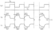
도 1은 본 발명의 일 실시예에 따른 DC-DC 컨버터를 나타내는 회로도이다. 도 2는 도 1의 스위칭 컨트롤러(10)를 나타내는 회로도이다. 도 3은 도 1의 DC-DC 컨버터의 입출력 신호를 나타내는 타이밍도이다. 도 4는 도 2의 스위치 게이트 구동부(12)의 입력 전압의 주기 및 슬루율 제어부(14)의 슬루율 변화 주기를 나타내는 타이밍도이다. 1 is a circuit diagram showing a DC-DC converter according to an embodiment of the present invention. 2 is a circuit diagram showing the switching
도 1 내지 도 4를 참조하면, 상기 DC-DC 컨버터는 턴 온 및 턴 오프를 반복하여 입력 DC 전압(VI)을 기초로 출력 DC 전압(VO)을 생성하는 파워 스위치(S) 및 상기 파워 스위치(S)의 동작을 제어하는 스위칭 컨트롤러(10)를 포함한다. 1 to 4, the DC-DC converter includes a power switch S for generating an output DC voltage VO based on an input DC voltage VI by repeating turn-on and turn-off, And a switching controller (10) for controlling the operation of the switch (S).
예를 들어, 상기 출력 DC 전압(VO)은 상기 입력 DC 전압(VI)보다 클 수 있다. For example, the output DC voltage VO may be greater than the input DC voltage VI.
상기 DC-DC 컨버터의 제1 입력 단 및 제2 입력 단 사이의 전압이 상기 입력 DC 전압(VI)이고, 상기 DC-DC 컨버터의 제1 출력 단과 제2 출력 단 사이의 전압이 상기 출력 DC 전압(VO)이다.Wherein a voltage between a first input terminal and a second input terminal of the DC-DC converter is the input DC voltage (VI), and a voltage between a first output terminal and a second output terminal of the DC- (VO).
상기 제1 입력 단에는 인덕터(L)의 제1 단이 연결된다. 상기 인덕터(L)의 제2 단은 상기 파워 스위치(S)의 입력 전극에 연결된다. 상기 파워 스위치(S)의 출력 전극은 상기 DC-DC 컨버터의 제2 입력 단에 연결된다. 상기 파워 스위치(S)의 제어 전극은 상기 스위칭 컨트롤러(10)에 연결된다. The first end of the inductor L is connected to the first input end. The second end of the inductor (L) is connected to the input electrode of the power switch (S). The output electrode of the power switch S is connected to the second input terminal of the DC-DC converter. The control electrode of the power switch S is connected to the switching
상기 파워 스위치(S)의 입력 전극은 다이오드(D)의 애노드에 연결된다. 상기 다이오드(D)의 캐소드는 상기 제1 출력 단에 연결된다.The input electrode of the power switch S is connected to the anode of the diode D. The cathode of the diode D is connected to the first output terminal.
상기 제1 출력 단에는 캐패시터(C)의 제1 단이 연결되고, 상기 제2 출력 단에는 상기 캐패시터(C)의 제2 단이 연결된다. The first end of the capacitor C is connected to the first output end, and the second end of the capacitor C is connected to the second output end.
상기 스위칭 컨트롤러(10)의 제1 단은 상기 제1 출력 단에 연결될 수 있다. 상기 스위칭 컨트롤러(10)의 제2 단은 상기 파워 스위치(S)의 제어 전극에 연결될 수 있다. The first end of the switching
상기 스위칭 컨트롤러(10)는 스위치 게이트 구동부(12) 및 슬루율 제어부(14)를 포함한다. The switching
상기 스위치 게이트 구동부(12)는 제1 주기(Ts)를 갖는 제1 전압(Vg1)의 레벨을 조절하여 상기 제1 주기(Ts)를 갖는 제2 전압(예컨대, 제1 노드(N1)의 전압)을 생성할 수 있다. The
상기 스위치 게이트 구동부(12)는 인버터(Q1) 및 버퍼(Q2, Q3)를 포함할 수 있다. 상기 스위치 게이트 구동부(12)의 제1 스위칭 소자(Q1)는 상기 제1 전압(Vg1)을 하이 레벨의 제1 DC 전압(Vc) 및 로우 레벨의 제2 DC 전압(예컨대 접지 전압)을 이용하여 반전시킨다. 예를 들어, 제2 노드(N2)의 전압은 상기 제1 전압(Vg1)으로부터 반전된 위상을 가질 수 있다. 또한, 상기 제2 노드(N2)의 전압은 상기 제1 전압(Vg1)보다 큰 레벨을 가질 수 있다. The
제2 스위칭 소자(Q2) 및 제3 스위칭 소자(Q3)는 상기 제2 노드(N2)의 전압을 버퍼링하여 상기 제1 노드(N1)로 출력한다. 상기 제2 전압(제1 노드(N1)의 전압)은 상기 제1 전압(Vg1)과 마찬가지로 제1 주기(Ts)를 갖는다. The second switching device Q2 and the third switching device Q3 buffer the voltage of the second node N2 and output the buffered voltage to the first node N1. The second voltage (the voltage of the first node N1) has a first period Ts as the first voltage Vg1.
구체적으로, 상기 제1 스위칭 소자(Q1)는 상기 제1 전압(Vg1)이 인가되는 제어 전극, 하이 레벨의 제1 DC 전압(Vc)이 인가되는 입력 전극 및 로우 레벨의 제2 DC 전압(예컨대 접지 전압)이 인가되는 출력 전극을 포함한다. Specifically, the first switching device Q1 includes a control electrode to which the first voltage Vg1 is applied, an input electrode to which a first DC voltage Vc of a high level is applied, and a second DC voltage Ground voltage) is applied.
상기 제2 스위칭 소자(Q2)는 상기 제1 스위칭 소자(Q1)의 상기 입력 전극에 연결되는 제어 전극, 상기 제1 DC 전압(Vc)이 인가되는 입력 전극 및 상기 제3 스위칭 소자(Q3)의 입력 전극에 연결되는 출력 전극을 포함한다. The second switching device Q2 includes a control electrode connected to the input electrode of the first switching device Q1, an input electrode to which the first DC voltage Vc is applied, And an output electrode connected to the input electrode.
상기 제3 스위칭 소자(Q3)는 상기 제1 스위칭 소자(Q1)의 상기 입력 전극에 연결되는 제어 전극, 상기 제2 스위칭 소자(Q2)의 상기 출력 전극에 연결되는 입력 전극 및 상기 제2 DC 전압이 인가되는 출력 전극을 포함한다. The third switching device Q3 includes a control electrode connected to the input electrode of the first switching device Q1, an input electrode connected to the output electrode of the second switching device Q2, And an output electrode to which a voltage is applied.
상기 슬루율 제어부(14)는 상기 파워 스위치(S)의 일단의 스위치 전압(VS)의 슬루율을 시간에 따라 가변시킨다. 슬루율이란 출력 신호 파형의 경사도를 의미하며, 일정 시간 동안 상기 출력 신호가 변화하는 양으로 정의될 수 있습니다. 슬루율이 크면 출력 신호가 빠르게 증가 및 감소함을 의미하고, 슬루율이 작으면 출력 신호가 느리게 증가 및 감소함을 의미한다.The slew
스위치 전압(VS)의 슬루율이 일정한 경우, 상기 파워 스위치(S)의 턴 온 및 턴 오프 시에 브로드 밴드 파워 노이즈가 발생할 수 있다. 상기 스위치 전압(VS)의 슬루율을 변화시켜주면 상기 파워 스위치(S)의 턴 온 및 턴 오프 시에 브로드 밴드 파워 노이즈를 감소시킬 수 있다. If the slew rate of the switch voltage VS is constant, broadband power noise may occur when the power switch S is turned on and off. By varying the slew rate of the switch voltage VS, it is possible to reduce the broadband power noise when the power switch S is turned on and off.
본 실시예의 슬루율 제어부(14)는 상기 스위치 전압(VS)의 슬루율을 시간에 따라 가변 시켜 상기 파워 스위치(S)의 턴 온 및 턴 오프 시에 브로드 밴드 파워 노이즈를 감소시킬 수 있다. The slew
상기 슬루율 제어부(14)는 병렬로 연결되는 N개의 저항들(R1 내지 RN)을 포함할 수 있다. 상기 N개의 저항들(R1 내지 RN)은 상기 N개의 저항들(R1 내지 RN)에 직렬로 연결되는 N개의 스위치들(SW1 내지 SWN)에 의해 상기 파워 스위치(S)와 상기 스위치 게이트 구동부(12)를 교대로 연결할 수 있다. The slew
예를 들어, t1에서 t2 사이에는 상기 제1 내지 제N 스위치(SW1 내지 SWN) 중 제1 스위치(SW1)가 턴 온 되어, 제1 저항(R1)이 상기 파워 스위치(S)와 상기 스위치 게이트 구동부(12) 사이에 연결된다. For example, the first switch SW1 of the first through the N-th switches SW1 through SWN is turned on between t1 and t2 so that the first resistor R1 is connected to the power switch S and the switch gate And is connected between the driving
예를 들어, t2에서 t3 사이에는 상기 제1 내지 제N 스위치(SW1 내지 SWN) 중 제2 스위치(SW2)가 턴 온 되어, 제2 저항(R2)이 상기 파워 스위치(S)와 상기 스위치 게이트 구동부(12) 사이에 연결된다.For example, between t2 and t3, the second switch SW2 of the first to the Nth switches SW1 to SWN is turned on, and the second resistor R2 is connected between the power switch S and the switch gate And is connected between the driving
예를 들어, t3에서 t4 사이에는 상기 제1 내지 제N 스위치(SW1 내지 SWN) 중 제3 스위치(SW3)가 턴 온 되어, 제3 저항(R3)이 상기 파워 스위치(S)와 상기 스위치 게이트 구동부(12) 사이에 연결된다.For example, between t3 and t4, the third switch SW3 of the first to the Nth switches SW1 to SWN is turned on, and the third resistor R3 is connected between the power switch S and the switch gate And is connected between the driving
예를 들어, tN에서 tN+1 사이에는 상기 제1 내지 제N 스위치(SW1 내지 SWN) 중 제N 스위치(SWN)가 턴 온 되어, 제N 저항(RN)이 상기 파워 스위치(S)와 상기 스위치 게이트 구동부(12) 사이에 연결된다.For example, the Nth switch SWN of the first to Nth switches SW1 to SWN is turned on between tN and tN + 1, and the Nth resistor RN is connected to the power switch S, Is connected between the switch gate driver (12).
상기 N개의 저항들(R1 내지 RN)은 서로 다른 저항 값을 가질 수 있다. 상기 슬루율 제어부(14)의 저항 값이 클수록 상기 스위치 전압(VS)의 슬루율이 낮아질 수 있다. The N resistors R1 to RN may have different resistance values. The larger the resistance value of the slew
본 실시예에서, 상기 제2 저항(R2)의 저항 값은 상기 제1 저항(R1)의 저항 값보다 크고, 상기 제3 저항(R3)의 저항 값은 상기 제2 저항(R2)의 저항 값보다 크고, 상기 제N 저항(RN)의 저항 값은 상기 제3 저항(R3)의 저항 값보다 클 수 있다. In this embodiment, the resistance value of the second resistor R2 is greater than the resistance value of the first resistor R1, and the resistance value of the third resistor R3 is greater than the resistance value of the second resistor R2 And the resistance value of the Nth resistor RN may be larger than the resistance value of the third resistor R3.
따라서, 도 3에서 보듯이, 상기 파워 스위치(S)와 상기 스위치 게이트 구동부(12) 사이에 저항 값이 가장 작은 상기 제1 저항(R1)이 연결되었을 때는 상기 슬루율 제어부(14)의 출력 전압(Vg)은 큰 슬루율을 갖는다. 따라서, 상기 스위치 전압(VS)은 큰 슬루율을 갖는다. 3, when the first resistor R1 having the smallest resistance value is connected between the power switch S and the
상기 파워 스위치(S)와 상기 스위치 게이트 구동부(12) 사이에 상기 제1 저항(R1)보다 큰 저항 값을 갖는 제2 저항(R2)이 연결되었을 때는 상기 슬루율 제어부(14)의 출력 전압(Vg)은 감소한다. 따라서, 상기 스위치 전압(VS)의 슬루율은 감소한다. When the second resistor R2 having a resistance value larger than the first resistor R1 is connected between the power switch S and the
상기 파워 스위치(S)와 상기 스위치 게이트 구동부(12) 사이에 상기 제2 저항(R2)보다 큰 저항 값을 갖는 제3 저항(R3)이 연결되었을 때는 상기 슬루율 제어부(14)의 출력 전압(Vg)은 감소한다. 따라서, 상기 스위치 전압(VS)의 슬루율은 감소한다. When the third resistor R3 having a resistance value larger than the second resistor R2 is connected between the power switch S and the
상기 파워 스위치(S)와 상기 스위치 게이트 구동부(12) 사이에 저항 값이 가장 큰 상기 제N 저항(RN)이 연결되었을 때는 상기 슬루율 제어부(14)의 출력 전압(Vg)은 가장 작은 슬루율을 갖는다. 따라서, 상기 스위치 전압(VS)은 가장 작은 슬루율을 갖는다.The output voltage Vg of the slew
본 실시예에서, 상기 슬루율 제어부(14)의 제1 스위치 내지 제N 스위치(SW1 내지 SWN)는 순차적으로 턴 온 되고, 상기 제N 스위치(SWN)가 턴 온 된 후 상기 제1 스위치(SW1)가 턴 온 된다. In the present embodiment, the first to nth switches SW1 to SWN of the slew
슬루율 변화 주기(Ta)는 상기 제1 스위치가 턴 온 되고, 다시 상기 제1 스위치가 턴 온 될 때까지의 시간으로 정의될 수 있다. 본 실시예에서, 상기 슬루율 변화 주기(Ta)는 상기 제1 주기(Ts)의 N배일 수 있다. The slew rate change period Ta may be defined as the time until the first switch is turned on and the first switch is turned on again. In the present embodiment, the slew rate change period Ta may be N times the first period Ts.
도 4에서 보듯이, 상기 슬루율 변화 주기(Ta)는 상기 제1 주기(Ts)의 N배의 정수배 중 어느 하나로 설정될 수 있다. 상기 브로드 밴드 노이즈를 가장 크게 감소시키기 위해서는 상기 슬루율 변화 주기(Ta)는 상기 제1 주기(Ts)의 N배로 설정될 수 있다. 반면, 상기 브로드 밴드 노이즈 감소의 필요성이 적은 경우에는 상기 슬루율 변화 주기(Ta)를 상기 제1 주기(Ts)의 2배, 4배 또는 m배로 설정할 수 있다. 상기 슬루율 변화 주기(Ta)를 크게 하면 상기 제1 내지 제N 스위치(SW1 내지 SWN)의 스위칭 횟수를 감소시킬 수 있으므로, 상기 슬루율 제어부(14)의 소비 전력을 감소시키고, 수명을 증가시킬 수 있다. As shown in FIG. 4, the slew rate change period Ta may be set to any integer multiple of N times the first period Ts. To largely reduce the broadband noise, the slew rate change period Ta may be set to N times the first period Ts. On the other hand, when the necessity of the broadband noise reduction is small, the slew rate change period Ta may be set to 2 times, 4 times, or m times the first period Ts. When the slew rate change period Ta is increased, the number of switching times of the first to Nth switches SW1 to SWN can be reduced, so that the power consumption of the slew
본 실시예에서는 상기 스위치 전압(VS)의 폴링 슬루율과 라이징 슬루율을 독립적으로 조절하지 않고, 상기 스위치 전압(VS)의 폴링 슬루율과 라이징 슬루율을 동일한 비율로 조절한다. In the present embodiment, the polling slew rate and the rising slew rate of the switch voltage VS are adjusted independently at the same ratio without adjusting the polling slew rate and the rising slew rate independently of each other.
예를 들어, 본 실시예에서는 상기 슬루율 제어부(14)의 제1 스위치(SW1)는 상기 제1 전압(Vg1)의 제1 펄스의 라이징 에지에 대응하여 턴 온 되고, 상기 슬루율 제어부(14)의 제2 스위치(SW2)는 상기 제1 전압(Vg1)의 제2 펄스의 라이징 에지에 대응하여 턴 온 된다. 이와는 달리, 상기 슬루율 제어부(14)의 제1 스위치(SW1)는 상기 제1 전압(Vg1)의 제1 펄스의 폴링 에지에 대응하여 턴 온 되고, 상기 슬루율 제어부(14)의 제2 스위치(SW2)는 상기 제1 전압(Vg1)의 제2 펄스의 폴링 에지에 대응하여 턴 온 된다. For example, in the present embodiment, the first switch SW1 of the slew
본 실시예에 따르면, 상기 DC-DC 컨버터는 시간에 따라 변화하는 슬루율을 갖는 전압을 생성하는 슬루율 제어부(14)를 포함하므로 브로드 밴드 파워 노이즈를 효과적으로 감소시킬 수 있다. According to the present embodiment, the DC-DC converter includes a slew
또한, 상기 슬루율 제어부(14)에 의해 상기 스위치 전압(VS)의 슬루율이 점진적으로 조절되므로, 피크 밴드 파워 노이즈의 발생을 방지할 수 있다. In addition, since the slew rate of the switch voltage VS is gradually adjusted by the slew
도 5는 본 발명의 다른 실시예에 따른 DC-DC 컨버터의 입출력 신호를 나타내는 타이밍도이다. 5 is a timing chart showing input / output signals of a DC-DC converter according to another embodiment of the present invention.
본 실시예에 따른 DC-DC 컨버터는 슬루율 변화 주기를 제외하면 도 1 내지 도 4를 참조하여 설명한 DC-DC 컨버터와 실질적으로 동일하다. 따라서, 동일하거나 대응되는 구성 요소에 대해서는 동일한 참조번호를 이용하고, 중복되는 설명은 생략한다.The DC-DC converter according to the present embodiment is substantially the same as the DC-DC converter described with reference to Figs. 1 to 4 except for the slew rate variation period. Therefore, the same reference numerals are used for the same or corresponding constituent elements, and redundant explanations are omitted.
도 1, 도 2 및 도 5를 참조하면, 상기 DC-DC 컨버터는 턴 온 및 턴 오프를 반복하여 입력 DC 전압(VI)을 기초로 출력 DC 전압(VO)을 생성하는 파워 스위치(S) 및 상기 파워 스위치(S)의 동작을 제어하는 스위칭 컨트롤러(10)를 포함한다. 1, 2 and 5, the DC-DC converter includes a power switch S for generating an output DC voltage VO based on an input DC voltage VI by repeating turn-on and turn- And a switching controller (10) for controlling the operation of the power switch (S).
상기 스위칭 컨트롤러(10)는 스위치 게이트 구동부(12) 및 슬루율 제어부(14)를 포함한다. The switching
상기 슬루율 제어부(14)는 상기 파워 스위치(S)의 일단의 스위치 전압(VS)의 슬루율을 시간에 따라 가변시킨다.The slew
본 실시예의 슬루율 제어부(14)는 상기 스위치 전압(VS)의 슬루율을 시간에 따라 가변 시켜 상기 파워 스위치(S)의 턴 온 및 턴 오프 시에 브로드 밴드 파워 노이즈를 감소시킬 수 있다. The slew
상기 슬루율 제어부(14)는 병렬로 연결되는 N개의 저항들(R1 내지 RN)을 포함할 수 있다. 상기 N개의 저항들(R1 내지 RN)은 상기 N개의 저항들(R1 내지 RN)에 직렬로 연결되는 N개의 스위치들(SW1 내지 SWN)에 의해 상기 파워 스위치(S)와 상기 스위치 게이트 구동부(12)를 교대로 연결할 수 있다. The slew
예를 들어, t1에서 t2 사이에는 상기 제1 내지 제N 스위치(SW1 내지 SWN) 중 제1 스위치(SW1)가 턴 온 되어, 제1 저항(R1)이 상기 파워 스위치(S)와 상기 스위치 게이트 구동부(12) 사이에 연결된다. For example, the first switch SW1 of the first through the N-th switches SW1 through SWN is turned on between t1 and t2 so that the first resistor R1 is connected to the power switch S and the switch gate And is connected between the driving
예를 들어, t2에서 t3 사이에는 상기 제1 내지 제N 스위치(SW1 내지 SWN) 중 제2 스위치(SW2)가 턴 온 되어, 제2 저항(R2)이 상기 파워 스위치(S)와 상기 스위치 게이트 구동부(12) 사이에 연결된다.For example, between t2 and t3, the second switch SW2 of the first to the Nth switches SW1 to SWN is turned on, and the second resistor R2 is connected between the power switch S and the switch gate And is connected between the driving
예를 들어, t3에서 t4 사이에는 상기 제1 내지 제N 스위치(SW1 내지 SWN) 중 제3 스위치(SW3)가 턴 온 되어, 제3 저항(R3)이 상기 파워 스위치(S)와 상기 스위치 게이트 구동부(12) 사이에 연결된다.For example, between t3 and t4, the third switch SW3 of the first to the Nth switches SW1 to SWN is turned on, and the third resistor R3 is connected between the power switch S and the switch gate And is connected between the driving
예를 들어, tN에서 tN+1 사이에는 상기 제1 내지 제N 스위치(SW1 내지 SWN) 중 제N 스위치(SWN)가 턴 온 되어, 제N 저항(RN)이 상기 파워 스위치(S)와 상기 스위치 게이트 구동부(12) 사이에 연결된다.For example, the Nth switch SWN of the first to Nth switches SW1 to SWN is turned on between tN and tN + 1, and the Nth resistor RN is connected to the power switch S, Is connected between the switch gate driver (12).
예를 들어, tN+1에서 tN+2 사이에는 상기 제1 내지 제N 스위치(SW1 내지 SWN) 중 제N-1 스위치가 턴 온 되어, 제N-1 저항이 상기 파워 스위치(S)와 상기 스위치 게이트 구동부(12) 사이에 연결된다.For example, an N-1th switch among the first to Nth switches SW1 to SWN is turned on between tN + 1 and tN + 2, and an N-1 resistor is connected between the power switch S and the Is connected between the switch gate driver (12).
예를 들어, t2N-3에서 t2N-2 사이에는 상기 제3 스위치(SW3)가 턴 온 되어, 상기 제3 저항(R3)이 상기 파워 스위치(S)와 상기 스위치 게이트 구동부(12) 사이에 연결된다.For example, the third switch SW3 is turned on between t2N-3 and t2N-2, and the third resistor R3 is connected between the power switch S and the
예를 들어, t2N-2에서 t2N-1 사이에는 상기 제2 스위치(SW2)가 턴 온 되어, 상기 제2 저항(R2)이 상기 파워 스위치(S)와 상기 스위치 게이트 구동부(12) 사이에 연결된다.For example, the second switch SW2 is turned on between t2N-2 and t2N-1, and the second resistor R2 is connected between the power switch S and the
예를 들어, t2N-1에서 t2N 사이에는 상기 제1 스위치(SW1)가 턴 온 되어, 상기 제1 저항(R1)이 상기 파워 스위치(S)와 상기 스위치 게이트 구동부(12) 사이에 연결된다.For example, the first switch SW1 is turned on between t2N-1 and t2N, and the first resistor R1 is connected between the power switch S and the
상기 N개의 저항들(R1 내지 RN)은 서로 다른 저항 값을 가질 수 있다. 상기 슬루율 제어부(14)의 저항 값이 클수록 상기 스위치 전압(VS)의 슬루율이 낮아질 수 있다. The N resistors R1 to RN may have different resistance values. The larger the resistance value of the slew
본 실시예에서, 상기 슬루율 제어부(14)의 제1 스위치 내지 제N 스위치(SW1 내지 SWN)는 순차적으로 턴 온 되고, 상기 제N 스위치(SWN)가 턴 온 된 후 제N-1 스위치 내지 상기 제1 스위치(SW1)가 순차적으로 턴 온 된다. In this embodiment, the first switch to the N-th switch (SW1 to SWN) of the slew
슬루율 변화 주기(Ta)는 상기 제1 스위치가 턴 온 되고, 다시 상기 제1 스위치가 턴 온 될 때까지의 시간으로 정의될 수 있다. 본 실시예에서, 상기 슬루율 변화 주기(Ta)는 상기 제1 주기(Ts)의 2N-2배일 수 있다. The slew rate change period Ta may be defined as the time until the first switch is turned on and the first switch is turned on again. In the present embodiment, the slew rate change period Ta may be 2N-2 times the first period Ts.
도시하지 않았으나, 상기 도 4에서와 같이, 상기 슬루율 변화 주기(Ta)는 상기 제1 주기(Ts)의 2N-2배의 정수배 중 어느 하나로 설정될 수 있다. As shown in FIG. 4, the slew rate change period Ta may be set to any integer multiple of 2N-2 times the first period Ts.
본 실시예에 따르면, 상기 DC-DC 컨버터는 시간에 따라 변화하는 슬루율을 갖는 전압을 생성하는 슬루율 제어부(14)를 포함하므로 브로드 밴드 파워 노이즈를 효과적으로 감소시킬 수 있다. According to the present embodiment, the DC-DC converter includes a slew
또한, 상기 슬루율 제어부(14)에 의해 상기 스위치 전압(VS)의 슬루율이 점진적으로 조절되므로, 피크 밴드 파워 노이즈의 발생을 방지할 수 있다. In addition, since the slew rate of the switch voltage VS is gradually adjusted by the slew
도 6은 본 발명의 다른 실시예에 따른 스위칭 컨트롤러의 슬루율 제어부를 나타내는 회로도이다. 도 7은 도 6의 스위칭 컨트롤러의 스위치 게이트 구동부(12)의 입력 전압의 주기 및 슬루율 제어부(14)의 슬루율 변화 주기를 나타내는 타이밍도이다.6 is a circuit diagram showing a slew rate control unit of a switching controller according to another embodiment of the present invention. 7 is a timing chart showing the period of the input voltage of the
본 실시예에 따른 DC-DC 컨버터는 슬루율 제어부는 폴링 슬루율과 라이징 슬루율을 독립적으로 제어하는 것을 제외하면 도 1 내지 도 4를 참조하여 설명한 DC-DC 컨버터와 실질적으로 동일하다. 따라서, 동일하거나 대응되는 구성 요소에 대해서는 동일한 참조번호를 이용하고, 중복되는 설명은 생략한다.The DC-DC converter according to the present embodiment is substantially the same as the DC-DC converter described with reference to Figs. 1 to 4 except that the slew rate control unit independently controls the polling slew rate and the rising slew rate. Therefore, the same reference numerals are used for the same or corresponding constituent elements, and redundant explanations are omitted.
도 1, 도 2 및 도 5를 참조하면, 상기 DC-DC 컨버터는 턴 온 및 턴 오프를 반복하여 입력 DC 전압(VI)을 기초로 출력 DC 전압(VO)을 생성하는 파워 스위치(S) 및 상기 파워 스위치(S)의 동작을 제어하는 스위칭 컨트롤러(10)를 포함한다. 1, 2 and 5, the DC-DC converter includes a power switch S for generating an output DC voltage VO based on an input DC voltage VI by repeating turn-on and turn- And a switching controller (10) for controlling the operation of the power switch (S).
상기 스위칭 컨트롤러(10)는 스위치 게이트 구동부(12) 및 슬루율 제어부(14)를 포함한다. The switching
상기 슬루율 제어부(14)는 상기 파워 스위치(S)의 일단의 스위치 전압(VS)의 슬루율을 시간에 따라 가변시킨다.The slew
본 실시예의 슬루율 제어부(14)는 상기 스위치 전압(VS)의 슬루율을 시간에 따라 가변 시켜 상기 파워 스위치(S)의 턴 온 및 턴 오프 시에 브로드 밴드 파워 노이즈를 감소시킬 수 있다. The slew
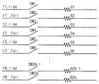
상기 슬루율 제어부(14)는 병렬로 연결되는 2N개의 저항들(R1 내지 R2N)을 포함할 수 있다. 상기 2N개의 저항들(R1 내지 R2N)은 상기 2N개의 저항들(R1 내지 R2N)에 직렬로 연결되는 2N개의 스위치들(SW1 내지 SW2N)에 의해 상기 파워 스위치(S)와 상기 스위치 게이트 구동부(12)를 교대로 연결할 수 있다. The slew
본 실시예에서는 상기 스위치 전압(VS)의 폴링 슬루율과 라이징 슬루율을 독립적으로 조절할 수 있다. 따라서, 상기 스위치 전압(VS)의 폴링 슬루율과 라이징 슬루율은 서로 다른 비율로 조절될 수 있다. In this embodiment, the polling slew rate and the rising slew rate of the switch voltage VS can be independently controlled. Therefore, the polling slew rate and the rising slew rate of the switch voltage VS can be adjusted at different ratios.
상기 슬루율 제어부(14)의 제1 스위치(SW1)는 상기 제1 전압(Vs)의 제1 펄스의 라이징 에지에 대응하여 턴 온 되고, 상기 슬루율 제어부(14)의 제2 스위치(SW2)는 상기 제1 전압(Vs)의 상기 제1 펄스의 폴링 에지에 대응하여 턴 온 될 수 있다. The first switch SW1 of the slew
상기 제1 전압(Vs)의 펄스들의 라이징 에지에 대응하여 순차적으로 턴 온 되는 제1 스위치 그룹(SW1, SW3, SW2N-1)의 반복 주기(Ta)는 상기 제1 전압의 상기 펄스들의 폴링 에지에 대응하여 순차적으로 턴 온 되는 제2 스위치 그룹(SW2, SW4, SW2N)의 반복 주기(Tb)와 상이할 수 있다. Wherein a repetition period (Ta) of the first switch group (SW1, SW3, SW2N-1) sequentially turned on in response to a rising edge of the pulse of the first voltage (Vs) May be different from the repetition period (Tb) of the second switch group (SW2, SW4, SW2N) sequentially turned on corresponding to the first switch group
도 7의 첫 번째 예시는 t1로부터 다음 t1까지의 라이징 슬루율 변화 주기(Ta)가 t1'로부터 다음 t1'까지의 폴링 슬루율 변화 주기(Tb)와 동일한 경우를 예시하였다. The first example of FIG. 7 illustrates a case where the rising slew rate change period Ta from t1 to t1 is equal to the polling slew rate change period Tb from t1 'to t1'.
이 경우, t1로부터 t1'사이에 제1 스위치(SW1)가 턴 온 되고, t1'로부터 t2 사이에 제2 스위치(SW2)가 턴 온 되며, t2로부터 t2' 사이에 제3 스위치(SW3)가 턴 온 되게 된다. In this case, the first switch SW1 is turned on between t1 and t1 ', the second switch SW2 is turned on between t1' and t2, and the third switch SW3 is turned on between t2 and t2 ' And turned on.
도 7의 두 번째 예시는 t1로부터 다음 t1까지의 라이징 슬루율 변화 주기(Ta)보다 t1'로부터 다음 t1'까지의 폴링 슬루율 변화 주기(Tb)가 큰 경우를 예시하였다. The second example of FIG. 7 illustrates a case where the polling slew rate change period (Tb) from t1 'to t1' is larger than the rising slew rate change period (Ta) from t1 to the next t1.
이 경우, t1로부터 t1'사이에 제1 스위치(SW1)가 턴 온 되고, t1'로부터 t2 사이에 제2 스위치(SW2)가 턴 온 되며, t2로부터 t3 사이에 제3 스위치(SW3)가 턴 온 되게 된다. In this case, the first switch SW1 is turned on between t1 and t1 ', the second switch SW2 is turned on between t1' and t2, and the third switch SW3 is turned on between t2 and t3 Is turned on.
도 7의 세 번째 예시는 t1로부터 다음 t1까지의 라이징 슬루율 변화 주기(Ta)가 t1'로부터 다음 t1'까지의 폴링 슬루율 변화 주기(Tb)보다 큰 경우를 예시하였다. The third example of FIG. 7 illustrates the case where the rising slew rate change period Ta from t1 to the next t1 is greater than the polling slew rate change period Tb from t1 'to the next t1'.
이 경우, t1로부터 t1'사이에 제1 스위치(SW1)가 턴 온 되고, t1'로부터 t2' 사이에 제2 스위치(SW2)가 턴 온 되며, t2'로부터 t2 사이에 제4 스위치(SW4)가 턴 온 되고, t2로부터 t3' 사이에 제3 스위치(SW3)가 턴 온 되게 된다. In this case, the first switch SW1 is turned on between t1 and t1 ', the second switch SW2 is turned on between t1' and t2 ', and the fourth switch SW4 is turned on between t2' The third switch SW3 is turned on between t2 and t3 '.
본 실시예에서는 상기 스위치 전압(VS)의 폴링 슬루율과 라이징 슬루율을 독립적으로 제어할 수 있다. 예를 들어, 상기 브로드 밴드 노이즈에 더욱 큰 영향을 주는 상기 스위치 전압(VS)의 상기 폴링 슬루율을 가변하고, 상기 스위치 전압(VS)의 상기 라이징 슬루율은 가변하지 않을 수 있다. In the present embodiment, the polling slew rate and the rising slew rate of the switch voltage VS can be independently controlled. For example, the polling slew rate of the switch voltage VS that has a greater effect on the broadband noise may be varied, and the rising slew rate of the switch voltage VS may not be variable.
본 실시예에 따르면, 상기 DC-DC 컨버터는 시간에 따라 변화하는 슬루율을 갖는 전압을 생성하는 슬루율 제어부(14)를 포함하므로 브로드 밴드 파워 노이즈를 효과적으로 감소시킬 수 있다. According to the present embodiment, the DC-DC converter includes a slew
또한, 상기 슬루율 제어부(14)에 의해 상기 스위치 전압(VS)의 슬루율이 점진적으로 조절되므로, 피크 밴드 파워 노이즈의 발생을 방지할 수 있다. In addition, since the slew rate of the switch voltage VS is gradually adjusted by the slew
도 8은 본 발명의 다른 실시예에 따른 DC-DC 컨버터의 스위칭 컨트롤러(10)를 나타내는 회로도이다. 도 9는 도 8의 DC-DC 컨버터의 입출력 신호를 나타내는 타이밍도이다.8 is a circuit diagram showing a switching
본 실시예에 따른 DC-DC 컨버터는 슬루율 제어부의 구성 및 동작을 제외하면 도 1 내지 도 4를 참조하여 설명한 DC-DC 컨버터와 실질적으로 동일하다. 따라서, 동일하거나 대응되는 구성 요소에 대해서는 동일한 참조번호를 이용하고, 중복되는 설명은 생략한다.The DC-DC converter according to this embodiment is substantially the same as the DC-DC converter described with reference to Figs. 1 to 4 except for the configuration and operation of the slew rate control unit. Therefore, the same reference numerals are used for the same or corresponding constituent elements, and redundant explanations are omitted.
도 1, 도 8 및 도 9를 참조하면, 상기 DC-DC 컨버터는 턴 온 및 턴 오프를 반복하여 입력 DC 전압(VI)을 기초로 출력 DC 전압(VO)을 생성하는 파워 스위치(S) 및 상기 파워 스위치(S)의 동작을 제어하는 스위칭 컨트롤러(10)를 포함한다. Referring to FIGS. 1, 8 and 9, the DC-DC converter includes a power switch S for generating an output DC voltage VO based on an input DC voltage VI by repeating turn-on and turn- And a switching controller (10) for controlling the operation of the power switch (S).
상기 스위칭 컨트롤러(10)는 스위치 게이트 구동부(12) 및 슬루율 제어부(14A)를 포함한다. The switching
상기 스위치 게이트 구동부(12)는 제1 주기(Ts)를 갖는 제1 전압(Vg1)의 레벨을 조절하여 상기 제1 주기(Ts)를 갖는 제2 전압(예컨대, 제1 노드(N1)의 전압)을 생성할 수 있다. The
상기 스위치 게이트 구동부(12)는 인버터(Q1) 및 버퍼(Q2, Q3)를 포함할 수 있다. 상기 스위치 게이트 구동부(12)의 제1 스위칭 소자(Q1)는 상기 제1 전압(Vg1)을 상기 슬루율 제어부(14A)에서 출력되는 가변 전원 전압(Vd) 및 로우 레벨의 제2 DC 전압(예컨대 접지 전압)을 이용하여 반전시킨다. 예를 들어, 제2 노드(N2)의 전압은 상기 제1 전압(Vg1)으로부터 반전된 위상을 가질 수 있다. 또한, 상기 제2 노드(N2)의 전압은 상기 제1 전압(Vg1)보다 큰 레벨을 가질 수 있다. The
제2 스위칭 소자(Q2) 및 제3 스위칭 소자(Q3)는 상기 제2 노드(N2)의 전압을 버퍼링하여 상기 제1 노드(N1)로 출력한다. 상기 제2 전압(제1 노드(N1)의 전압)은 상기 제1 전압(Vg1)과 마찬가지로 제1 주기(Ts)를 갖는다. The second switching device Q2 and the third switching device Q3 buffer the voltage of the second node N2 and output the buffered voltage to the first node N1. The second voltage (the voltage of the first node N1) has a first period Ts as the first voltage Vg1.
구체적으로, 상기 제1 스위칭 소자(Q1)는 상기 제1 전압(Vg1)이 인가되는 제어 전극, 상기 가변 전원 전압(Vd)이 인가되는 입력 전극 및 로우 레벨의 제2 DC 전압(예컨대 접지 전압)이 인가되는 출력 전극을 포함한다. Specifically, the first switching device Q1 includes a control electrode to which the first voltage Vg1 is applied, an input electrode to which the variable power supply voltage Vd is applied, and a second DC voltage (e.g., a ground voltage) And an output electrode to which a voltage is applied.
상기 제2 스위칭 소자(Q2)는 상기 제1 스위칭 소자(Q1)의 상기 입력 전극에 연결되는 제어 전극, 하이 레벨의 제1 DC 전압(Vc1)이 인가되는 입력 전극 및 상기 제3 스위칭 소자(Q3)의 입력 전극에 연결되는 출력 전극을 포함한다. The second switching device Q2 includes a control electrode connected to the input electrode of the first switching device Q1, an input electrode to which a first DC voltage Vc1 of a high level is applied, And an output electrode connected to the input electrode of the transistor.
상기 제3 스위칭 소자(Q3)는 상기 제1 스위칭 소자(Q1)의 상기 입력 전극에 연결되는 제어 전극, 상기 제2 스위칭 소자(Q2)의 상기 출력 전극에 연결되는 입력 전극 및 상기 제2 DC 전압이 인가되는 출력 전극을 포함한다. The third switching device Q3 includes a control electrode connected to the input electrode of the first switching device Q1, an input electrode connected to the output electrode of the second switching device Q2, And an output electrode to which a voltage is applied.
상기 슬루율 제어부(14A)는 상기 파워 스위치(S)의 일단의 스위치 전압(VS)의 슬루율을 시간에 따라 가변시킨다.The slew
본 실시예의 슬루율 제어부(14A)는 상기 스위치 전압(VS)의 슬루율을 시간에 따라 가변 시켜 상기 파워 스위치(S)의 턴 온 및 턴 오프 시에 브로드 밴드 파워 노이즈를 감소시킬 수 있다. The slew
상기 슬루율 제어부(14A)는 입력 신호에 따라 서로 다른 레벨을 갖는 가변 전원 전압(Vd)을 생성한다. 상기 슬루율 제어부(14A)는 입력 신호를 생성하여 디지털-아날로그 컨버터(DAC, 142)에 출력하는 컨트롤부(141), 상기 입력 신호를 수신하여 입력 아날로그 신호를 생성하는 디지털-아날로그 컨버터(142), 상기 디지털-아날로그 컨버터(142)에 연결되는 증폭기(AMP) 및 상기 증폭기(AMP)에 연결되는 제4 스위칭 소자(Q4)를 포함할 수 있다. The slew
구체적으로, 상기 증폭기(AMP)의 제1 입력 전극은 상기 디지털-아날로그 컨버터(DAC)의 출력 단에 연결되고, 상기 증폭기(AMP)의 제2 입력 전극에는 로우 레벨의 전원 전압(예컨대, 접지 전압)이 인가되고, 상기 증폭기(AMP)의 출력 전극은 상기 제4 스위칭 소자(Q4)의 제어 전극에 연결될 수 있다. In detail, the first input electrode of the amplifier AMP is connected to the output terminal of the digital-analog converter DAC, and the second input electrode of the amplifier AMP is supplied with a low-level supply voltage And the output electrode of the amplifier AMP may be connected to the control electrode of the fourth switching device Q4.
상기 제4 스위칭 소자(Q4)의 입력 전극은 로드 저항(RC)의 제1 단에 연결될 수 있다. 상기 로드 저항(RC)의 제2 단에는 하이 레벨의 제3 DC 전압(Vc2)이 인가될 수 있다. The input electrode of the fourth switching device Q4 may be connected to the first end of the load resistor RC. And a high level third DC voltage Vc2 may be applied to the second end of the load resistor RC.
상기 스위치 게이트 구동부(12)의 제1 전압(Vg1)이 로우 레벨을 가질 때, 제2 노드(N2) 전압은 상기 가변 전원 전압(Vd)의 레벨을 갖고, 상기 스위치 게이트 구동부(12)의 제1 전압(Vg1)이 하이 레벨을 가질 때, 상기 제2 노드(N2) 전압은 로우 레벨을 갖는다. When the first voltage Vg1 of the
상기 제1 노드(N1)에는 상기 제2 노드(N2) 전압이 버퍼링되어 전달된다. 따라서, 상기 제1 노드(N1)의 전압(Vg)은 상기 제2 노드(N2)의 전압과 실질적으로 동일한 파형을 갖는다. The second node N2 is buffered and transferred to the first node N1. Therefore, the voltage Vg of the first node N1 has a waveform substantially equal to the voltage of the second node N2.
상기 제1 노드(N1)의 전압(Vg)은 상기 파워 스위치(S)의 제어 전극에 인가된다. 상기 제1 노드(N1)의 전압(Vg)의 하이 레벨이 높은 값을 갖는 경우, 상기 파워 스위치(S)의 상기 스위치 전압(VS)의 슬루율이 높아진다.The voltage Vg of the first node N1 is applied to the control electrode of the power switch S. When the high level of the voltage Vg of the first node N1 has a high value, the slew rate of the switch voltage VS of the power switch S becomes high.
도 9를 보면, t1과 t2 사이에 상기 제1 노드(N1)의 전압(Vg)은 가장 높은 하이 레벨(Vd1)을 갖는다. 따라서, 상기 스위치 전압(VS)의 슬루율은 가장 크다. Referring to Fig. 9, the voltage Vg of the first node N1 has the highest high level Vd1 between t1 and t2. Therefore, the slew rate of the switch voltage VS is the largest.
t2와 t3 사이에 상기 제1 노드(N1)의 전압(Vg)은 상기 Vd1에서 Vd2로 감소한다. 따라서, 상기 스위치 전압(VS)의 슬루율은 감소한다. the voltage Vg of the first node N1 decreases from Vd1 to Vd2 between t2 and t3. Therefore, the slew rate of the switch voltage VS decreases.
t3과 t4 사이에 상기 제1 노드(N1)의 전압(Vg)은 상기 Vd2에서 Vd3으로 감소한다. 따라서, 상기 스위치 전압(VS)의 슬루율은 감소한다. the voltage Vg of the first node N1 decreases from Vd2 to Vd3 between t3 and t4. Therefore, the slew rate of the switch voltage VS decreases.
tN과 tN+1 사이에 상기 제1 노드(N1)의 전압(Vg)은 가장 낮은 하이 레벨(VdN)을 갖는다. 따라서, 상기 스위치 전압(VS)의 슬루율은 가장 작다.the voltage Vg of the first node N1 between the tN and the tN + 1 has the lowest high level VdN. Therefore, the slew rate of the switch voltage VS is the smallest.
본 실시예에서, 상기 가변 전원 전압의 레벨은 제1 레벨(Vd1)로부터 제N 레벨(VdN)까지 순차적으로 감소하고, 상기 가변 전원 전압이 상기 제N 레벨(VdN)에 도달한 후 상기 제1 레벨(Vd1)로 증가한다. In this embodiment, the level of the variable power supply voltage sequentially decreases from the first level (Vd1) to the Nth level (VdN), and after the variable power supply voltage reaches the Nth level (VdN) Level (Vd1).
슬루율 변화 주기(Ta)는 상기 제1 레벨(Vd1)로부터 상기 제N 레벨(VdN)까지 감소하였다가 다시 상기 제1 레벨(Vd1)로 돌아올 때까지의 시간으로 정의될 수 있다. 본 실시예에서, 상기 슬루율 변화 주기(Ta)는 상기 제1 주기(Ts)의 N배일 수 있다. The slew rate change period Ta may be defined as the time from the first level Vd1 to the Nth level VdN until the first level Vd1 returns to the first level Vd1. In the present embodiment, the slew rate change period Ta may be N times the first period Ts.
도시하지 않았으나, 상기 도 4에서와 같이, 상기 슬루율 변화 주기(Ta)는 상기 제1 주기(Ts)의 N배의 정수배 중 어느 하나로 설정될 수 있다. As shown in FIG. 4, the slew rate change period Ta may be set to any integer multiple of N times the first period Ts.
본 실시예에 따르면, 상기 DC-DC 컨버터는 시간에 따라 변화하는 슬루율을 갖는 전압을 생성하는 슬루율 제어부(14)를 포함하므로 브로드 밴드 파워 노이즈를 효과적으로 감소시킬 수 있다. According to the present embodiment, the DC-DC converter includes a slew
또한, 상기 슬루율 제어부(14)에 의해 상기 스위치 전압(VS)의 슬루율이 점진적으로 조절되므로, 피크 밴드 파워 노이즈의 발생을 방지할 수 있다. In addition, since the slew rate of the switch voltage VS is gradually adjusted by the slew
도 10은 본 발명의 다른 실시예에 따른 DC-DC 컨버터의 입출력 신호를 나타내는 타이밍도이다.10 is a timing chart showing input / output signals of a DC-DC converter according to another embodiment of the present invention.
본 실시예에 따른 DC-DC 컨버터는 슬루율 변화 주기를 제외하면 도 8 및 도 9를 참조하여 설명한 DC-DC 컨버터와 실질적으로 동일하다. 따라서, 동일하거나 대응되는 구성 요소에 대해서는 동일한 참조번호를 이용하고, 중복되는 설명은 생략한다.The DC-DC converter according to the present embodiment is substantially the same as the DC-DC converter described with reference to Figs. 8 and 9 except for the slew rate variation period. Therefore, the same reference numerals are used for the same or corresponding constituent elements, and redundant explanations are omitted.
도 1, 도 8 및 도 10을 참조하면, 상기 DC-DC 컨버터는 턴 온 및 턴 오프를 반복하여 입력 DC 전압(VI)을 기초로 출력 DC 전압(VO)을 생성하는 파워 스위치(S) 및 상기 파워 스위치(S)의 동작을 제어하는 스위칭 컨트롤러(10)를 포함한다. Referring to FIGS. 1, 8 and 10, the DC-DC converter includes a power switch S for generating an output DC voltage VO based on an input DC voltage VI by repeating turn-on and turn- And a switching controller (10) for controlling the operation of the power switch (S).
상기 스위칭 컨트롤러(10)는 스위치 게이트 구동부(12) 및 슬루율 제어부(14)를 포함한다. The switching
상기 슬루율 제어부(14)는 상기 파워 스위치(S)의 일단의 스위치 전압(VS)의 슬루율을 시간에 따라 가변시킨다.The slew
본 실시예의 슬루율 제어부(14)는 상기 스위치 전압(VS)의 슬루율을 시간에 따라 가변 시켜 상기 파워 스위치(S)의 턴 온 및 턴 오프 시에 브로드 밴드 파워 노이즈를 감소시킬 수 있다. The slew
상기 슬루율 제어부(14A)는 입력 신호에 따라 서로 다른 레벨을 갖는 가변 전원 전압(Vd)을 생성한다. 상기 슬루율 제어부(14A)는 입력 신호를 생성하여 디지털-아날로그 컨버터(DAC, 142)에 출력하는 컨트롤부(141), 상기 입력 신호를 수신하여 입력 아날로그 신호를 생성하는 디지털-아날로그 컨버터(142), 상기 디지털-아날로그 컨버터(142)에 연결되는 증폭기(AMP) 및 상기 증폭기(AMP)에 연결되는 제4 스위칭 소자(Q4)를 포함할 수 있다. The slew
도 10을 보면, t1과 t2 사이에 상기 제1 노드(N1)의 전압(Vg)은 가장 높은 하이 레벨(Vd1)을 갖는다. 따라서, 상기 스위치 전압(VS)의 슬루율은 가장 크다. 10, the voltage Vg of the first node N1 has the highest high level Vd1 between t1 and t2. Therefore, the slew rate of the switch voltage VS is the largest.
t2와 t3 사이에 상기 제1 노드(N1)의 전압(Vg)은 상기 Vd1에서 Vd2로 감소한다. 따라서, 상기 스위치 전압(VS)의 슬루율은 감소한다. the voltage Vg of the first node N1 decreases from Vd1 to Vd2 between t2 and t3. Therefore, the slew rate of the switch voltage VS decreases.
t3과 t4 사이에 상기 제1 노드(N1)의 전압(Vg)은 상기 Vd2에서 Vd3으로 감소한다. 따라서, 상기 스위치 전압(VS)의 슬루율은 감소한다. the voltage Vg of the first node N1 decreases from Vd2 to Vd3 between t3 and t4. Therefore, the slew rate of the switch voltage VS decreases.
tN과 tN+1 사이에 상기 제1 노드(N1)의 전압(Vg)은 가장 낮은 하이 레벨(VdN)을 갖는다. 따라서, 상기 스위치 전압(VS)의 슬루율은 가장 작다.the voltage Vg of the first node N1 between the tN and the tN + 1 has the lowest high level VdN. Therefore, the slew rate of the switch voltage VS is the smallest.
tN+1과 tN+2 사이에 상기 제1 노드(N1)의 전압(Vg)은 VdN에서 VdN+1로 증가한다. 따라서, 상기 스위치 전압(VS)의 슬루율은 증가한다.the voltage Vg of the first node N1 increases from VdN to VdN + 1 between tN + 1 and tN + 2. Therefore, the slew rate of the switch voltage VS increases.
t2N-3과 t2N-2 사이에 상기 제1 노드(N1)의 전압(Vg)은 Vd3으로 증가한다. 따라서, 상기 스위치 전압(VS)의 슬루율은 증가한다.the voltage Vg of the first node N1 between t2N-3 and t2N-2 increases to Vd3. Therefore, the slew rate of the switch voltage VS increases.
t2N-2와 t2N-1 사이에 상기 제1 노드(N1)의 전압(Vg)은 Vd3에서 Vd2로 증가한다. 따라서, 상기 스위치 전압(VS)의 슬루율은 증가한다.the voltage Vg of the first node N1 between t2N-2 and t2N-1 increases from Vd3 to Vd2. Therefore, the slew rate of the switch voltage VS increases.
t2N-1과 t2N 사이에 상기 제1 노드(N1)의 전압(Vg)은 Vd2에서 최대값인 Vd1로 증가한다. 따라서, 상기 스위치 전압(VS)의 슬루율은 가장 크다. the voltage Vg of the first node N1 between t2N-1 and t2N increases from Vd2 to the maximum value Vd1. Therefore, the slew rate of the switch voltage VS is the largest.
본 실시예에서, 상기 가변 전원 전압의 레벨은 제1 레벨(Vd1)로부터 제N 레벨(VdN)까지 순차적으로 감소하고, 상기 가변 전원 전압이 상기 제N 레벨(VdN)에 도달한 후 제N-1 레벨로부터 상기 제1 레벨까지 순차적으로 증가한다. In the present embodiment, the level of the variable power supply voltage sequentially decreases from the first level Vd1 to the N-th level VdN, and after the variable power supply voltage reaches the N-th level VdN, 1 < / RTI > level to the first level.
슬루율 변화 주기(Ta)는 상기 제1 레벨(Vd1)로부터 상기 제N 레벨(VdN)까지 감소하였다가 다시 상기 제1 레벨(Vd1)로 돌아올 때까지의 시간으로 정의될 수 있다. 본 실시예에서, 상기 슬루율 변화 주기(Ta)는 상기 제1 주기(Ts)의 2N-2배일 수 있다.The slew rate change period Ta may be defined as the time from the first level Vd1 to the Nth level VdN until the first level Vd1 returns to the first level Vd1. In the present embodiment, the slew rate change period Ta may be 2N-2 times the first period Ts.
도시하지 않았으나, 상기 도 4에서와 같이, 상기 슬루율 변화 주기(Ta)는 상기 제1 주기(Ts)의 2N-2배의 정수배 중 어느 하나로 설정될 수 있다. As shown in FIG. 4, the slew rate change period Ta may be set to any integer multiple of 2N-2 times the first period Ts.
본 실시예에 따르면, 상기 DC-DC 컨버터는 시간에 따라 변화하는 슬루율을 갖는 전압을 생성하는 슬루율 제어부(14)를 포함하므로 브로드 밴드 파워 노이즈를 효과적으로 감소시킬 수 있다. According to the present embodiment, the DC-DC converter includes a slew
또한, 상기 슬루율 제어부(14)에 의해 상기 스위치 전압(VS)의 슬루율이 점진적으로 조절되므로, 피크 밴드 파워 노이즈의 발생을 방지할 수 있다. In addition, since the slew rate of the switch voltage VS is gradually adjusted by the slew
도 11은 본 발명의 일 실시예에 따른 표시 장치를 나타내는 블록도이다.11 is a block diagram showing a display device according to an embodiment of the present invention.
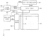
도 1 내지 도 11을 참조하면, 상기 표시 장치는 표시 패널(100) 및 패널 구동부를 포함한다. 상기 패널 구동부는 타이밍 컨트롤러(200), 게이트 구동부(300), 감마 기준 전압 생성부(400), 데이터 구동부(500) 및 전원 전압 생성부(600)를 포함한다. 1 to 11, the display device includes a
상기 표시 패널(100)은 영상을 표시하는 표시부 및 상기 표시부에 이웃하여 배치되는 주변부를 포함한다. The
상기 표시 패널(100)은 복수의 게이트 라인들(GL), 복수의 데이터 라인들(DL) 및 상기 게이트 라인들(GL)과 상기 데이터 라인들(DL) 각각에 전기적으로 연결된 복수의 단위 픽셀들을 포함한다. 상기 게이트 라인들(GL)은 제1 방향(D1)으로 연장되고, 상기 데이터 라인들(DL)은 상기 제1 방향(D1)과 교차하는 제2 방향(D2)으로 연장된다. The
각 단위 픽셀은 스위칭 소자(미도시), 상기 스위칭 소자에 전기적으로 연결된 액정 캐패시터(미도시) 및 스토리지 캐패시터(미도시)를 포함할 수 있다. 상기 단위 픽셀들은 매트릭스 형태로 배치될 수 있다.Each unit pixel may include a switching element (not shown), a liquid crystal capacitor (not shown) electrically connected to the switching element, and a storage capacitor (not shown). The unit pixels may be arranged in a matrix form.
상기 타이밍 컨트롤러(200)는 외부의 장치(미도시)로부터 입력 영상 데이터(RGB) 및 입력 제어 신호(CONT)를 수신한다. 상기 입력 영상 데이터는 적색 영상 데이터(R), 녹색 영상 데이터(G) 및 청색 영상 데이터(B)를 포함할 수 있다. 상기 입력 제어 신호(CONT)는 마스터 클럭 신호, 데이터 인에이블 신호를 포함할 수 있다. 상기 입력 제어 신호(CONT)는 수직 동기 신호 및 수평 동기 신호를 더 포함할 수 있다. The
상기 타이밍 컨트롤러(200)는 상기 입력 영상 데이터(RGB) 및 상기 입력 제어 신호(CONT)를 근거로 제1 제어 신호(CONT1), 제2 제어 신호(CONT2), 제3 제어 신호(CONT3) 및 데이터 신호(DATA)를 생성한다. The
상기 타이밍 컨트롤러(200)는 상기 입력 제어 신호(CONT)를 근거로 상기 게이트 구동부(300)의 동작을 제어하기 위한 상기 제1 제어 신호(CONT1)를 생성하여 상기 게이트 구동부(300)에 출력한다. 상기 제1 제어 신호(CONT1)는 수직 개시 신호 및 게이트 클럭 신호를 포함할 수 있다.The
상기 타이밍 컨트롤러(200)는 상기 입력 제어 신호(CONT)를 근거로 상기 데이터 구동부(500)의 동작을 제어하기 위한 상기 제2 제어 신호(CONT2)를 생성하여 상기 데이터 구동부(500)에 출력한다. 상기 제2 제어 신호(CONT2)는 수평 개시 신호 및 로드 신호를 포함할 수 있다.The
상기 타이밍 컨트롤러(200)는 상기 입력 영상 데이터(RGB)를 근거로 데이터 신호(DATA)를 생성한다. 상기 타이밍 컨트롤러(200)는 상기 데이터 신호(DATA)를 상기 데이터 구동부(500)에 출력한다. The
상기 타이밍 컨트롤러(200)는 상기 입력 제어 신호(CONT)를 근거로 상기 감마 기준 전압 생성부(400)의 동작을 제어하기 위한 상기 제3 제어 신호(CONT3)를 생성하여 상기 감마 기준 전압 생성부(400)에 출력한다. The
상기 게이트 구동부(300)는 상기 타이밍 컨트롤러(200)로부터 입력 받은 상기 제1 제어 신호(CONT1)에 응답하여 상기 게이트 라인들(GL)을 구동하기 위한 게이트 신호들을 생성한다. 상기 게이트 구동부(300)는 상기 게이트 신호들을 상기 게이트 라인들(GL)에 순차적으로 출력한다. The
상기 감마 기준 전압 생성부(400)는 상기 타이밍 컨트롤러(200)로부터 입력 받은 상기 제3 제어 신호(CONT3)에 응답하여 감마 기준 전압(VGREF)을 생성한다. 상기 감마 기준 전압 생성부(400)는 상기 감마 기준 전압(VGREF)을 상기 데이터 구동부(500)에 제공한다. 상기 감마 기준 전압(VGREF)은 각각의 데이터 신호(DATA)에 대응하는 값을 갖는다. The gamma reference voltage generator 400 generates the gamma reference voltage VGREF in response to the third control signal CONT3 received from the
본 발명의 일 실시예에서, 상기 감마 기준 전압 생성부(400)는 상기 타이밍 컨트롤러(200) 내에 배치되거나 상기 데이터 구동부(500) 내에 배치될 수 있다.In an embodiment of the present invention, the gamma reference voltage generator 400 may be disposed in the
상기 데이터 구동부(500)는 상기 타이밍 컨트롤러(200)로부터 상기 제2 제어 신호(CONT2) 및 상기 데이터 신호(DATA)를 입력 받고, 상기 감마 기준 전압 생성부(400)로부터 상기 감마 기준 전압(VGREF)을 입력 받는다. 상기 데이터 구동부(500)는 상기 데이터 신호(DATA)를 상기 감마 기준 전압(VGREF)을 이용하여 아날로그 형태의 데이터 전압으로 변환한다. 상기 데이터 구동부(500)는 상기 데이터 전압을 상기 데이터 라인(DL)에 출력한다. The
상기 전원 전압 생성부(600)는 도 1 내지 도 10을 참조하여 설명한 DC-DC 컨버터를 포함할 수 있다. 상기 DC-DC 컨버터는 턴 온 및 턴 오프를 반복하여 입력 DC 전압(VI)을 기초로 출력 DC 전압(VO)을 생성하는 파워 스위치(S) 및 상기 파워 스위치(S)의 동작을 제어하는 스위칭 컨트롤러(10)를 포함한다. The power
예를 들어, 상기 DC-DC 컨버터의 상기 출력 DC 전압은 상기 게이트 신호의 하이 레벨을 정의하는 게이트 온 전압(VON)일 수 있다. 상기 게이트 구동부(300)는 상기 게이트 온 전압(VON)을 이용하여 상기 게이트 신호를 생성하여 상기 표시 패널(100)의 상기 게이트 라인(GL)에 출력할 수 있다. For example, the output DC voltage of the DC-DC converter may be a gate-on voltage (VON) defining a high level of the gate signal. The
예를 들어, 상기 DC-DC 컨버터의 상기 출력 DC 전압은 상기 데이터 전압을 생성하기 위한 아날로그 하이 전원 전압(AVDD)일 수 있다. 상기 데이터 구동부(500)는 상기 아날로그 하이 전원 전압(AVDD)을 이용하여 상기 데이터 전압을 생성하여 상기 표시 패널(100)의 상기 데이터 라인(DL)에 출력할 수 있다.For example, the output DC voltage of the DC-DC converter may be an analog high supply voltage (AVDD) for generating the data voltage. The
본 실시예에 따르면, 상기 DC-DC 컨버터는 시간에 따라 변화하는 슬루율을 갖는 전압을 생성하는 슬루율 제어부(14)를 포함하므로 표시 장치의 브로드 밴드 파워 노이즈를 효과적으로 감소시킬 수 있다. According to the present embodiment, since the DC-DC converter includes the slew
또한, 상기 슬루율 제어부(14)에 의해 상기 스위치 전압(VS)의 슬루율이 점진적으로 조절되므로, 표시 장치의 피크 밴드 파워 노이즈의 발생을 방지할 수 있다. In addition, since the slew rate of the switch voltage VS is gradually adjusted by the slew
이상에서 설명한 본 발명에 따른 DC-DC 컨버터 및 이를 포함하는 표시 장치에 따르면, 노이즈를 효과적으로 제거할 수 있다. According to the DC-DC converter and the display device including the DC-DC converter according to the present invention, noise can be effectively removed.
이상 실시예들을 참조하여 설명하였지만, 해당 기술 분야의 숙련된 당업자는 하기의 특허 청구의 범위에 기재된 본 발명의 사상 및 영역으로부터 벗어나지 않는 범위 내에서 본 발명을 다양하게 수정 및 변경시킬 수 있음을 이해할 수 있을 것이다.It will be understood by those skilled in the art that various changes in form and details may be made therein without departing from the spirit and scope of the invention as defined in the appended claims. It will be possible.
10: 스위칭 컨트롤러
12: 스위치 게이트 구동부
14, 14A: 슬루율 제어부
141: 컨트롤부
142: 디지털-아날로그 컨버터
100: 표시 패널
200: 타이밍 컨트롤러
300: 게이트 구동부
400: 감마 기준 전압 생성부
500: 데이터 구동부
600: 전원 전압 생성부10: Switching controller 12: Switch gate driver
14, 14A: Slew rate control unit 141:
142: Digital-to-analog converter 100: Display panel
200: timing controller 300: gate driver
400: gamma reference voltage generator 500:
600: Power supply voltage generating section
Claims (20)
상기 파워 스위치의 동작을 제어하는 스위칭 컨트롤러를 포함하고,
상기 스위칭 컨트롤러는 상기 파워 스위치의 일단의 스위치 전압의 슬루율을 시간에 따라 가변시키는 슬루율 제어부를 포함하는 것을 특징으로 하는 DC-DC 컨버터.A power switch that repeats turn-on and turn-off to generate an output DC voltage based on an input DC voltage; And
And a switching controller for controlling operation of the power switch,
Wherein the switching controller includes a slew rate control unit that varies a slew rate of a switch voltage at one end of the power switch with time.
상기 N개의 저항들은 상기 N개의 저항들에 직렬로 연결되는 N개의 스위치들에 의해 상기 파워 스위치와 상기 스위치 게이트 구동부를 교대로 연결하는 것을 특징으로 하는 DC-DC 컨버터.The apparatus of claim 2, wherein the slew rate control unit includes N resistors connected in parallel,
Wherein the N resistors alternately connect the power switch and the switch gate driver by N switches serially connected to the N resistors.
상기 제N 스위치가 턴 온 된 후 상기 제1 스위치가 턴 온 되며,
상기 제1 스위치가 턴 온 되고, 다시 상기 제1 스위치가 턴 온 될 때까지의 시간으로 정의되는 슬루율 변화 주기는 상기 제1 주기의 N배인 것을 특징으로 하는 DC-DC 컨버터.The method of claim 3, wherein the first switch to the Nth switch of the slew rate control unit are sequentially turned on,
The first switch is turned on after the Nth switch is turned on,
Wherein a slew rate change period defined as a time until the first switch is turned on and the first switch is turned on is N times the first period.
상기 제N 스위치가 턴 온 된 후 제N-1 스위치 내지 상기 제1 스위치가 순차적으로 턴 온 되며,
상기 제1 스위치가 턴 온 되고, 다시 상기 제1 스위치가 턴 온 될 때까지의 시간으로 정의되는 슬루율 변화 주기는 상기 제1 주기의 2N-2배인 것을 특징으로 하는 DC-DC 컨버터.The method of claim 3, wherein the first switch to the Nth switch of the slew rate control unit are sequentially turned on,
The Nth switch and the first switch are sequentially turned on after the Nth switch is turned on,
Wherein the slew rate change period defined by a time from when the first switch is turned on to when the first switch is turned on is 2N-2 times the first period.
상기 제1 스위칭 소자는 상기 제1 전압이 인가되는 제어 전극, 하이 레벨의 제1 DC 전압이 인가되는 입력 전극 및 로우 레벨의 제2 DC 전압이 인가되는 출력 전극을 포함하고,
상기 제2 스위칭 소자는 상기 제1 스위칭 소자의 상기 입력 전극에 연결되는 제어 전극, 상기 제1 DC 전압이 인가되는 입력 전극 및 상기 제3 스위칭 소자의 입력 전극에 연결되는 출력 전극을 포함하며,
상기 제3 스위칭 소자는 상기 제1 스위칭 소자의 상기 입력 전극에 연결되는 제어 전극, 상기 제2 스위칭 소자의 상기 출력 전극에 연결되는 입력 전극 및 상기 제2 DC 전압이 인가되는 출력 전극을 포함하는 것을 특징으로 하는 DC-DC 컨버터.4. The semiconductor memory device according to claim 3, wherein the switch gate driver includes a first switching element, a second switching element, and a third switching element,
The first switching device includes a control electrode to which the first voltage is applied, an input electrode to which a first DC voltage of a high level is applied, and an output electrode to which a second DC voltage of a low level is applied,
The second switching element includes a control electrode connected to the input electrode of the first switching element, an input electrode to which the first DC voltage is applied, and an output electrode connected to the input electrode of the third switching element,
The third switching device may include a control electrode connected to the input electrode of the first switching device, an input electrode connected to the output electrode of the second switching device, and an output electrode to which the second DC voltage is applied Features a DC-DC converter.
상기 입력 신호를 수신하여 입력 아날로그 신호를 생성하는 디지털-아날로그 컨버터;
상기 디지털-아날로그 컨버터에 연결되는 증폭기; 및
상기 증폭기에 연결되는 제4 스위칭 소자를 포함하는 것을 특징으로 하는 DC-DC 컨버터.13. The apparatus of claim 12, wherein the slew rate controller
A digital-to-analog converter for receiving the input signal and generating an input analog signal;
An amplifier coupled to the digital-to-analog converter; And
And a fourth switching element connected to the amplifier.
상기 가변 전원 전압이 상기 제N 레벨에 도달한 후 상기 제1 레벨로 증가하며,
상기 가변 전원 전압이 상기 제1 레벨로부터 상기 제N 레벨까지 감소하였다가 다시 상기 제1 레벨로 돌아올 때까지의 시간으로 정의되는 슬루율 변화 주기는 상기 제1 주기의 N배인 것을 특징으로 하는 DC-DC 컨버터.13. The method of claim 12, wherein the level of the variable power supply voltage is sequentially decreased from the first level to the N-th level,
The variable power supply voltage is increased to the first level after reaching the Nth level,
Wherein the slew rate change period defined by the time from when the variable power supply voltage decreases from the first level to the N-th level and then returns to the first level is N times the first period. DC converter.
상기 가변 전원 전압이 상기 제N 레벨에 도달한 후 제N-1 레벨로부터 상기 제1 레벨까지 순차적으로 증가하며,
상기 가변 전원 전압이 상기 제1 레벨로부터 상기 제N 레벨까지 감소하였다가 다시 상기 제1 레벨로 돌아올 때까지의 시간으로 정의되는 슬루율 변화 주기는 상기 제1 주기의 2N-2배인 것을 특징으로 하는 DC-DC 컨버터.13. The method of claim 12, wherein the level of the variable power supply voltage is sequentially decreased from the first level to the N-th level,
And sequentially increases from the (N-1) th level to the first level after the variable power supply voltage reaches the Nth level,
Wherein the slew rate change period defined by a time from when the variable power supply voltage decreases from the first level to the Nth level and then returns to the first level is 2N-2 times the first period. DC-DC converter.
상기 제1 스위칭 소자는 상기 제1 전압이 인가되는 제어 전극, 상기 가변 전원 전압이 인가되는 입력 전극 및 로우 레벨의 제2 DC 전압이 인가되는 출력 전극을 포함하고,
상기 제2 스위칭 소자는 상기 제1 스위칭 소자의 상기 입력 전극에 연결되는 제어 전극, 하이 레벨의 제1 DC 전압이 인가되는 입력 전극 및 상기 제3 스위칭 소자의 입력 전극에 연결되는 출력 전극을 포함하며,
상기 제3 스위칭 소자는 상기 제1 스위칭 소자의 상기 입력 전극에 연결되는 제어 전극, 상기 제2 스위칭 소자의 상기 출력 전극에 연결되는 입력 전극 및 상기 제2 DC 전압이 인가되는 출력 전극을 포함하는 것을 특징으로 하는 DC-DC 컨버터.13. The semiconductor memory device according to claim 12, wherein the switch gate driver includes a first switching element, a second switching element, and a third switching element,
Wherein the first switching element includes a control electrode to which the first voltage is applied, an input electrode to which the variable power supply voltage is applied, and an output electrode to which a second DC voltage of a low level is applied,
The second switching device includes a control electrode connected to the input electrode of the first switching device, an input electrode to which a first DC voltage of a high level is applied, and an output electrode connected to an input electrode of the third switching device ,
The third switching device may include a control electrode connected to the input electrode of the first switching device, an input electrode connected to the output electrode of the second switching device, and an output electrode to which the second DC voltage is applied Features a DC-DC converter.
턴 온 및 턴 오프를 반복하여 입력 DC 전압을 기초로 출력 DC 전압을 생성하는 파워 스위치 및 상기 파워 스위치의 동작을 제어하는 스위칭 컨트롤러를 포함하는 DC-DC 컨버터; 및
상기 출력 DC 전압을 기초로 상기 표시 패널을 구동하는 표시 패널 구동부를 포함하고,
상기 스위칭 컨트롤러는 상기 파워 스위치의 일단의 스위치 전압의 슬루율을 시간에 따라 가변시키는 슬루율 제어부를 포함하는 것을 특징으로 하는 표시 장치.A display panel for displaying an image;
A DC-DC converter including a power switch that repeats turn-on and turn-off to generate an output DC voltage based on an input DC voltage, and a switching controller that controls operation of the power switch; And
And a display panel driver for driving the display panel based on the output DC voltage,
Wherein the switching controller includes a slew rate controller for varying a slew rate of a switch voltage at one end of the power switch according to time.
상기 DC-DC 컨버터의 상기 출력 DC 전압은 상기 게이트 신호의 하이 레벨을 정의하는 게이트 온 전압인 것을 특징으로 하는 표시 장치.The display device of claim 18, wherein the display panel driver includes a gate driver for outputting a gate signal to a gate line of the display panel,
And the output DC voltage of the DC-DC converter is a gate-on voltage that defines a high level of the gate signal.
상기 DC-DC 컨버터의 상기 출력 DC 전압은 상기 데이터 전압을 생성하기 위한 아날로그 하이 전원 전압인 것을 특징으로 하는 표시 장치.
19. The display panel driving apparatus according to claim 18, wherein the display panel driver includes a data driver for outputting a data voltage to a data line of the display panel,
Wherein the output DC voltage of the DC-DC converter is an analog high supply voltage for generating the data voltage.
Priority Applications (3)
| Application Number | Priority Date | Filing Date | Title |
|---|---|---|---|
| KR1020140144511A KR102240284B1 (en) | 2014-10-23 | 2014-10-23 | Dc-dc converter and display apparatus having the same |
| CN201510688237.8A CN105553270B (en) | 2014-10-23 | 2015-10-21 | DC-DC converter and display device with DC-DC converter |
| US14/920,176 US10083671B2 (en) | 2014-10-23 | 2015-10-22 | DC-DC converter and display apparatus having the same |
Applications Claiming Priority (1)
| Application Number | Priority Date | Filing Date | Title |
|---|---|---|---|
| KR1020140144511A KR102240284B1 (en) | 2014-10-23 | 2014-10-23 | Dc-dc converter and display apparatus having the same |
Publications (2)
| Publication Number | Publication Date |
|---|---|
| KR20160048314A true KR20160048314A (en) | 2016-05-04 |
| KR102240284B1 KR102240284B1 (en) | 2021-04-15 |
Family
ID=55792780
Family Applications (1)
| Application Number | Title | Priority Date | Filing Date |
|---|---|---|---|
| KR1020140144511A KR102240284B1 (en) | 2014-10-23 | 2014-10-23 | Dc-dc converter and display apparatus having the same |
Country Status (3)
| Country | Link |
|---|---|
| US (1) | US10083671B2 (en) |
| KR (1) | KR102240284B1 (en) |
| CN (1) | CN105553270B (en) |
Cited By (2)
| Publication number | Priority date | Publication date | Assignee | Title |
|---|---|---|---|---|
| KR20190065725A (en) * | 2017-12-04 | 2019-06-12 | 엘지전자 주식회사 | Converter and power converting apparatus including same |
| US10522070B2 (en) | 2016-11-03 | 2019-12-31 | Samsung Display Co., Ltd. | Converter and display apparatus including the same |
Families Citing this family (3)
| Publication number | Priority date | Publication date | Assignee | Title |
|---|---|---|---|---|
| KR102450738B1 (en) * | 2017-11-20 | 2022-10-05 | 삼성전자주식회사 | Source driving circuit and display device including the same |
| US10840795B1 (en) * | 2019-10-16 | 2020-11-17 | Monolithic Power Systems, Inc. | Power transistor driver with reduced spikes for switching converters |
| CN113470590A (en) * | 2021-07-15 | 2021-10-01 | Tcl华星光电技术有限公司 | Logic circuit and display panel |
Citations (4)
| Publication number | Priority date | Publication date | Assignee | Title |
|---|---|---|---|---|
| JP2011078193A (en) * | 2009-09-30 | 2011-04-14 | Sharp Corp | Video display device |
| JP2011091923A (en) * | 2009-10-21 | 2011-05-06 | Mitsubishi Electric Corp | Drive circuit of voltage-driven switching device |
| JP2012129971A (en) * | 2010-11-22 | 2012-07-05 | Denso Corp | Load drive device |
| JP2014011830A (en) * | 2012-06-28 | 2014-01-20 | Hitachi Appliances Inc | Power conversion device |
Family Cites Families (19)
| Publication number | Priority date | Publication date | Assignee | Title |
|---|---|---|---|---|
| US5636114A (en) | 1995-11-30 | 1997-06-03 | Electronic Measurements, Inc. | Lossless snubber circuit for use in power converters |
| US6335638B1 (en) | 2000-06-29 | 2002-01-01 | Pericom Semiconductor Corp. | Triple-slope clock driver for reduced EMI |
| US6434029B1 (en) | 2001-10-17 | 2002-08-13 | Astec International Limited | Boost topology having an auxiliary winding on the snubber inductor |
| TW556401B (en) | 2002-02-01 | 2003-10-01 | Potrans Electrical Corp | Converter using synchronous rectification circuit and associated with LC snubber apparatus |
| JP2005165604A (en) | 2003-12-02 | 2005-06-23 | Seiko Instruments Inc | Overshoot recovering circuit, and voltage regulator |
| US7190225B2 (en) | 2004-09-23 | 2007-03-13 | Maxim Integrated Products, Inc. | Efficient low EMI switching output stages and methods |
| US7852053B2 (en) * | 2005-10-31 | 2010-12-14 | Chil Semiconductor Corporation | Power supply and controller circuits |
| US7489117B2 (en) * | 2005-10-31 | 2009-02-10 | Chil Semiconductor Corporation | Dynamic conversion circuit for a voltage regulator module |
| US7777461B2 (en) * | 2005-10-31 | 2010-08-17 | Chil Semiconductor Corporation | Power supply and controller circuits |
| US7456618B2 (en) * | 2005-10-31 | 2008-11-25 | Chil Semiconductor, Inc. | Digital controller for a voltage regulator module |
| US7592789B2 (en) * | 2005-10-31 | 2009-09-22 | Chil Semiconductor Corporation | Power supply and related circuits |
| US8723438B2 (en) | 2007-03-12 | 2014-05-13 | Cirrus Logic, Inc. | Switch power converter control with spread spectrum based electromagnetic interference reduction |
| KR101229462B1 (en) | 2007-04-25 | 2013-02-05 | 어드밴스드 아날로직 테크놀로지스 인코퍼레이티드 | Step-down switching regulator with freewheeling diode |
| US7923974B2 (en) * | 2008-01-04 | 2011-04-12 | Chil Semiconductor Corporation | Modification of switch activation order in a power supply |
| WO2011145706A1 (en) | 2010-05-21 | 2011-11-24 | Semiconductor Energy Laboratory Co., Ltd. | Semiconductor device and display device |
| US9093903B2 (en) * | 2011-09-28 | 2015-07-28 | Monolithic Power Systems, Inc. | Power converter with voltage window and the method thereof |
| JP2013150453A (en) | 2012-01-19 | 2013-08-01 | Renesas Electronics Corp | Controller |
| KR101989575B1 (en) * | 2012-12-07 | 2019-06-14 | 삼성전자주식회사 | Adaptive power converting device |
| JP6231314B2 (en) * | 2013-07-16 | 2017-11-15 | シナプティクス・ジャパン合同会社 | Display drive device |
-
2014
- 2014-10-23 KR KR1020140144511A patent/KR102240284B1/en active IP Right Grant
-
2015
- 2015-10-21 CN CN201510688237.8A patent/CN105553270B/en active Active
- 2015-10-22 US US14/920,176 patent/US10083671B2/en active Active
Patent Citations (4)
| Publication number | Priority date | Publication date | Assignee | Title |
|---|---|---|---|---|
| JP2011078193A (en) * | 2009-09-30 | 2011-04-14 | Sharp Corp | Video display device |
| JP2011091923A (en) * | 2009-10-21 | 2011-05-06 | Mitsubishi Electric Corp | Drive circuit of voltage-driven switching device |
| JP2012129971A (en) * | 2010-11-22 | 2012-07-05 | Denso Corp | Load drive device |
| JP2014011830A (en) * | 2012-06-28 | 2014-01-20 | Hitachi Appliances Inc | Power conversion device |
Cited By (3)
| Publication number | Priority date | Publication date | Assignee | Title |
|---|---|---|---|---|
| US10522070B2 (en) | 2016-11-03 | 2019-12-31 | Samsung Display Co., Ltd. | Converter and display apparatus including the same |
| US10796624B2 (en) | 2016-11-03 | 2020-10-06 | Samsung Display Co., Ltd. | Converter and display apparatus including the same |
| KR20190065725A (en) * | 2017-12-04 | 2019-06-12 | 엘지전자 주식회사 | Converter and power converting apparatus including same |
Also Published As
| Publication number | Publication date |
|---|---|
| CN105553270A (en) | 2016-05-04 |
| US20160118875A1 (en) | 2016-04-28 |
| CN105553270B (en) | 2019-10-15 |
| KR102240284B1 (en) | 2021-04-15 |
| US10083671B2 (en) | 2018-09-25 |
Similar Documents
| Publication | Publication Date | Title |
|---|---|---|
| US9143148B2 (en) | Amplification circuit, source driver, electrooptical device, and electronic device | |
| EP2393191B1 (en) | Boost converter for liquid crystal display | |
| KR102240284B1 (en) | Dc-dc converter and display apparatus having the same | |
| US20070040825A1 (en) | Display device | |
| JP2009271530A (en) | Source driver and display device including the same | |
| KR20030084728A (en) | Display driving device and display using the same | |
| WO2013098899A1 (en) | Shift register | |
| US20110102406A1 (en) | Gate driver and operating method thereof | |
| US20020080131A1 (en) | Display driving apparatus and display apparatus module | |
| TWI488170B (en) | Display the drive circuit of the panel | |
| JP2009300866A (en) | Driving circuit and display device | |
| KR101347165B1 (en) | Liquid crystal display device | |
| US20090009452A1 (en) | Display control device and method of controlling same | |
| KR102554201B1 (en) | Display driver ic and display apparatus including the same | |
| KR102534116B1 (en) | Dc to dc converter and display apparatus having the same | |
| KR20060081572A (en) | Method of driving source driver for lcd | |
| KR20150047961A (en) | Dcdc converter, display apparatus having the same and method of driving display panel using the same | |
| KR20090105148A (en) | Display apparatus | |
| KR20150088598A (en) | Data driver and display apparatus having the same and method of driving display panel using the same | |
| WO2016011678A1 (en) | Digital-to-analog converter, programmable gamma correction buffer circuit and display device | |
| TW201608549A (en) | Display devices | |
| CN115966170A (en) | Slew rate controller and driving method thereof | |
| JP2011018012A (en) | Control method for image display apparatus | |
| JP2009251046A (en) | Image display apparatus and control method of the same | |
| KR102151058B1 (en) | Circuit for modulation gate pulse and display device including the same |
Legal Events
| Date | Code | Title | Description |
|---|---|---|---|
| A201 | Request for examination | ||
| E902 | Notification of reason for refusal | ||
| E701 | Decision to grant or registration of patent right | ||
| GRNT | Written decision to grant |