KR20160041969A - Multi-die fine grain integrated voltage regulation - Google Patents
Multi-die fine grain integrated voltage regulation Download PDFInfo
- Publication number
- KR20160041969A KR20160041969A KR1020167005750A KR20167005750A KR20160041969A KR 20160041969 A KR20160041969 A KR 20160041969A KR 1020167005750 A KR1020167005750 A KR 1020167005750A KR 20167005750 A KR20167005750 A KR 20167005750A KR 20160041969 A KR20160041969 A KR 20160041969A
- Authority
- KR
- South Korea
- Prior art keywords
- semiconductor device
- passive
- power
- terminals
- semiconductor
- Prior art date
Links
Images


Classifications
-
- H—ELECTRICITY
- H01—ELECTRIC ELEMENTS
- H01L—SEMICONDUCTOR DEVICES NOT COVERED BY CLASS H10
- H01L27/00—Devices consisting of a plurality of semiconductor or other solid-state components formed in or on a common substrate
- H01L27/02—Devices consisting of a plurality of semiconductor or other solid-state components formed in or on a common substrate including semiconductor components specially adapted for rectifying, oscillating, amplifying or switching and having at least one potential-jump barrier or surface barrier; including integrated passive circuit elements with at least one potential-jump barrier or surface barrier
- H01L27/04—Devices consisting of a plurality of semiconductor or other solid-state components formed in or on a common substrate including semiconductor components specially adapted for rectifying, oscillating, amplifying or switching and having at least one potential-jump barrier or surface barrier; including integrated passive circuit elements with at least one potential-jump barrier or surface barrier the substrate being a semiconductor body
- H01L27/10—Devices consisting of a plurality of semiconductor or other solid-state components formed in or on a common substrate including semiconductor components specially adapted for rectifying, oscillating, amplifying or switching and having at least one potential-jump barrier or surface barrier; including integrated passive circuit elements with at least one potential-jump barrier or surface barrier the substrate being a semiconductor body including a plurality of individual components in a repetitive configuration
- H01L27/101—Devices consisting of a plurality of semiconductor or other solid-state components formed in or on a common substrate including semiconductor components specially adapted for rectifying, oscillating, amplifying or switching and having at least one potential-jump barrier or surface barrier; including integrated passive circuit elements with at least one potential-jump barrier or surface barrier the substrate being a semiconductor body including a plurality of individual components in a repetitive configuration including resistors or capacitors only
-
- H—ELECTRICITY
- H01—ELECTRIC ELEMENTS
- H01G—CAPACITORS; CAPACITORS, RECTIFIERS, DETECTORS, SWITCHING DEVICES OR LIGHT-SENSITIVE DEVICES, OF THE ELECTROLYTIC TYPE
- H01G4/00—Fixed capacitors; Processes of their manufacture
- H01G4/002—Details
- H01G4/228—Terminals
-
- H—ELECTRICITY
- H01—ELECTRIC ELEMENTS
- H01G—CAPACITORS; CAPACITORS, RECTIFIERS, DETECTORS, SWITCHING DEVICES OR LIGHT-SENSITIVE DEVICES, OF THE ELECTROLYTIC TYPE
- H01G4/00—Fixed capacitors; Processes of their manufacture
- H01G4/002—Details
- H01G4/228—Terminals
- H01G4/232—Terminals electrically connecting two or more layers of a stacked or rolled capacitor
-
- H—ELECTRICITY
- H01—ELECTRIC ELEMENTS
- H01G—CAPACITORS; CAPACITORS, RECTIFIERS, DETECTORS, SWITCHING DEVICES OR LIGHT-SENSITIVE DEVICES, OF THE ELECTROLYTIC TYPE
- H01G4/00—Fixed capacitors; Processes of their manufacture
- H01G4/38—Multiple capacitors, i.e. structural combinations of fixed capacitors
-
- H—ELECTRICITY
- H01—ELECTRIC ELEMENTS
- H01G—CAPACITORS; CAPACITORS, RECTIFIERS, DETECTORS, SWITCHING DEVICES OR LIGHT-SENSITIVE DEVICES, OF THE ELECTROLYTIC TYPE
- H01G4/00—Fixed capacitors; Processes of their manufacture
- H01G4/40—Structural combinations of fixed capacitors with other electric elements, the structure mainly consisting of a capacitor, e.g. RC combinations
-
- H—ELECTRICITY
- H01—ELECTRIC ELEMENTS
- H01L—SEMICONDUCTOR DEVICES NOT COVERED BY CLASS H10
- H01L23/00—Details of semiconductor or other solid state devices
- H01L23/12—Mountings, e.g. non-detachable insulating substrates
- H01L23/13—Mountings, e.g. non-detachable insulating substrates characterised by the shape
-
- H—ELECTRICITY
- H01—ELECTRIC ELEMENTS
- H01L—SEMICONDUCTOR DEVICES NOT COVERED BY CLASS H10
- H01L23/00—Details of semiconductor or other solid state devices
- H01L23/48—Arrangements for conducting electric current to or from the solid state body in operation, e.g. leads, terminal arrangements ; Selection of materials therefor
- H01L23/481—Internal lead connections, e.g. via connections, feedthrough structures
-
- H—ELECTRICITY
- H01—ELECTRIC ELEMENTS
- H01L—SEMICONDUCTOR DEVICES NOT COVERED BY CLASS H10
- H01L23/00—Details of semiconductor or other solid state devices
- H01L23/48—Arrangements for conducting electric current to or from the solid state body in operation, e.g. leads, terminal arrangements ; Selection of materials therefor
- H01L23/488—Arrangements for conducting electric current to or from the solid state body in operation, e.g. leads, terminal arrangements ; Selection of materials therefor consisting of soldered or bonded constructions
- H01L23/498—Leads, i.e. metallisations or lead-frames on insulating substrates, e.g. chip carriers
- H01L23/49811—Additional leads joined to the metallisation on the insulating substrate, e.g. pins, bumps, wires, flat leads
- H01L23/49816—Spherical bumps on the substrate for external connection, e.g. ball grid arrays [BGA]
-
- H—ELECTRICITY
- H01—ELECTRIC ELEMENTS
- H01L—SEMICONDUCTOR DEVICES NOT COVERED BY CLASS H10
- H01L23/00—Details of semiconductor or other solid state devices
- H01L23/58—Structural electrical arrangements for semiconductor devices not otherwise provided for, e.g. in combination with batteries
- H01L23/64—Impedance arrangements
- H01L23/642—Capacitive arrangements
-
- H—ELECTRICITY
- H01—ELECTRIC ELEMENTS
- H01L—SEMICONDUCTOR DEVICES NOT COVERED BY CLASS H10
- H01L24/00—Arrangements for connecting or disconnecting semiconductor or solid-state bodies; Methods or apparatus related thereto
- H01L24/01—Means for bonding being attached to, or being formed on, the surface to be connected, e.g. chip-to-package, die-attach, "first-level" interconnects; Manufacturing methods related thereto
- H01L24/10—Bump connectors ; Manufacturing methods related thereto
- H01L24/12—Structure, shape, material or disposition of the bump connectors prior to the connecting process
- H01L24/14—Structure, shape, material or disposition of the bump connectors prior to the connecting process of a plurality of bump connectors
-
- H—ELECTRICITY
- H01—ELECTRIC ELEMENTS
- H01L—SEMICONDUCTOR DEVICES NOT COVERED BY CLASS H10
- H01L24/00—Arrangements for connecting or disconnecting semiconductor or solid-state bodies; Methods or apparatus related thereto
- H01L24/01—Means for bonding being attached to, or being formed on, the surface to be connected, e.g. chip-to-package, die-attach, "first-level" interconnects; Manufacturing methods related thereto
- H01L24/26—Layer connectors, e.g. plate connectors, solder or adhesive layers; Manufacturing methods related thereto
- H01L24/31—Structure, shape, material or disposition of the layer connectors after the connecting process
- H01L24/32—Structure, shape, material or disposition of the layer connectors after the connecting process of an individual layer connector
-
- H—ELECTRICITY
- H01—ELECTRIC ELEMENTS
- H01L—SEMICONDUCTOR DEVICES NOT COVERED BY CLASS H10
- H01L24/00—Arrangements for connecting or disconnecting semiconductor or solid-state bodies; Methods or apparatus related thereto
- H01L24/73—Means for bonding being of different types provided for in two or more of groups H01L24/10, H01L24/18, H01L24/26, H01L24/34, H01L24/42, H01L24/50, H01L24/63, H01L24/71
-
- H—ELECTRICITY
- H01—ELECTRIC ELEMENTS
- H01L—SEMICONDUCTOR DEVICES NOT COVERED BY CLASS H10
- H01L25/00—Assemblies consisting of a plurality of individual semiconductor or other solid state devices ; Multistep manufacturing processes thereof
- H01L25/03—Assemblies consisting of a plurality of individual semiconductor or other solid state devices ; Multistep manufacturing processes thereof all the devices being of a type provided for in the same subgroup of groups H01L27/00 - H01L33/00, or in a single subclass of H10K, H10N, e.g. assemblies of rectifier diodes
- H01L25/04—Assemblies consisting of a plurality of individual semiconductor or other solid state devices ; Multistep manufacturing processes thereof all the devices being of a type provided for in the same subgroup of groups H01L27/00 - H01L33/00, or in a single subclass of H10K, H10N, e.g. assemblies of rectifier diodes the devices not having separate containers
- H01L25/065—Assemblies consisting of a plurality of individual semiconductor or other solid state devices ; Multistep manufacturing processes thereof all the devices being of a type provided for in the same subgroup of groups H01L27/00 - H01L33/00, or in a single subclass of H10K, H10N, e.g. assemblies of rectifier diodes the devices not having separate containers the devices being of a type provided for in group H01L27/00
- H01L25/0652—Assemblies consisting of a plurality of individual semiconductor or other solid state devices ; Multistep manufacturing processes thereof all the devices being of a type provided for in the same subgroup of groups H01L27/00 - H01L33/00, or in a single subclass of H10K, H10N, e.g. assemblies of rectifier diodes the devices not having separate containers the devices being of a type provided for in group H01L27/00 the devices being arranged next and on each other, i.e. mixed assemblies
-
- H—ELECTRICITY
- H01—ELECTRIC ELEMENTS
- H01L—SEMICONDUCTOR DEVICES NOT COVERED BY CLASS H10
- H01L25/00—Assemblies consisting of a plurality of individual semiconductor or other solid state devices ; Multistep manufacturing processes thereof
- H01L25/03—Assemblies consisting of a plurality of individual semiconductor or other solid state devices ; Multistep manufacturing processes thereof all the devices being of a type provided for in the same subgroup of groups H01L27/00 - H01L33/00, or in a single subclass of H10K, H10N, e.g. assemblies of rectifier diodes
- H01L25/04—Assemblies consisting of a plurality of individual semiconductor or other solid state devices ; Multistep manufacturing processes thereof all the devices being of a type provided for in the same subgroup of groups H01L27/00 - H01L33/00, or in a single subclass of H10K, H10N, e.g. assemblies of rectifier diodes the devices not having separate containers
- H01L25/065—Assemblies consisting of a plurality of individual semiconductor or other solid state devices ; Multistep manufacturing processes thereof all the devices being of a type provided for in the same subgroup of groups H01L27/00 - H01L33/00, or in a single subclass of H10K, H10N, e.g. assemblies of rectifier diodes the devices not having separate containers the devices being of a type provided for in group H01L27/00
- H01L25/0657—Stacked arrangements of devices
-
- H—ELECTRICITY
- H01—ELECTRIC ELEMENTS
- H01L—SEMICONDUCTOR DEVICES NOT COVERED BY CLASS H10
- H01L25/00—Assemblies consisting of a plurality of individual semiconductor or other solid state devices ; Multistep manufacturing processes thereof
- H01L25/16—Assemblies consisting of a plurality of individual semiconductor or other solid state devices ; Multistep manufacturing processes thereof the devices being of types provided for in two or more different main groups of groups H01L27/00 - H01L33/00, or in a single subclass of H10K, H10N, e.g. forming hybrid circuits
-
- H—ELECTRICITY
- H01—ELECTRIC ELEMENTS
- H01L—SEMICONDUCTOR DEVICES NOT COVERED BY CLASS H10
- H01L25/00—Assemblies consisting of a plurality of individual semiconductor or other solid state devices ; Multistep manufacturing processes thereof
- H01L25/18—Assemblies consisting of a plurality of individual semiconductor or other solid state devices ; Multistep manufacturing processes thereof the devices being of types provided for in two or more different subgroups of the same main group of groups H01L27/00 - H01L33/00, or in a single subclass of H10K, H10N
-
- H—ELECTRICITY
- H01—ELECTRIC ELEMENTS
- H01L—SEMICONDUCTOR DEVICES NOT COVERED BY CLASS H10
- H01L28/00—Passive two-terminal components without a potential-jump or surface barrier for integrated circuits; Details thereof; Multistep manufacturing processes therefor
- H01L28/40—Capacitors
-
- H—ELECTRICITY
- H01—ELECTRIC ELEMENTS
- H01L—SEMICONDUCTOR DEVICES NOT COVERED BY CLASS H10
- H01L28/00—Passive two-terminal components without a potential-jump or surface barrier for integrated circuits; Details thereof; Multistep manufacturing processes therefor
- H01L28/40—Capacitors
- H01L28/60—Electrodes
-
- H—ELECTRICITY
- H01—ELECTRIC ELEMENTS
- H01L—SEMICONDUCTOR DEVICES NOT COVERED BY CLASS H10
- H01L2224/00—Indexing scheme for arrangements for connecting or disconnecting semiconductor or solid-state bodies and methods related thereto as covered by H01L24/00
- H01L2224/01—Means for bonding being attached to, or being formed on, the surface to be connected, e.g. chip-to-package, die-attach, "first-level" interconnects; Manufacturing methods related thereto
- H01L2224/02—Bonding areas; Manufacturing methods related thereto
- H01L2224/04—Structure, shape, material or disposition of the bonding areas prior to the connecting process
- H01L2224/0401—Bonding areas specifically adapted for bump connectors, e.g. under bump metallisation [UBM]
-
- H—ELECTRICITY
- H01—ELECTRIC ELEMENTS
- H01L—SEMICONDUCTOR DEVICES NOT COVERED BY CLASS H10
- H01L2224/00—Indexing scheme for arrangements for connecting or disconnecting semiconductor or solid-state bodies and methods related thereto as covered by H01L24/00
- H01L2224/01—Means for bonding being attached to, or being formed on, the surface to be connected, e.g. chip-to-package, die-attach, "first-level" interconnects; Manufacturing methods related thereto
- H01L2224/10—Bump connectors; Manufacturing methods related thereto
- H01L2224/12—Structure, shape, material or disposition of the bump connectors prior to the connecting process
- H01L2224/13—Structure, shape, material or disposition of the bump connectors prior to the connecting process of an individual bump connector
- H01L2224/13001—Core members of the bump connector
- H01L2224/1302—Disposition
- H01L2224/13025—Disposition the bump connector being disposed on a via connection of the semiconductor or solid-state body
-
- H—ELECTRICITY
- H01—ELECTRIC ELEMENTS
- H01L—SEMICONDUCTOR DEVICES NOT COVERED BY CLASS H10
- H01L2224/00—Indexing scheme for arrangements for connecting or disconnecting semiconductor or solid-state bodies and methods related thereto as covered by H01L24/00
- H01L2224/01—Means for bonding being attached to, or being formed on, the surface to be connected, e.g. chip-to-package, die-attach, "first-level" interconnects; Manufacturing methods related thereto
- H01L2224/10—Bump connectors; Manufacturing methods related thereto
- H01L2224/12—Structure, shape, material or disposition of the bump connectors prior to the connecting process
- H01L2224/14—Structure, shape, material or disposition of the bump connectors prior to the connecting process of a plurality of bump connectors
- H01L2224/1401—Structure
- H01L2224/1403—Bump connectors having different sizes, e.g. different diameters, heights or widths
-
- H—ELECTRICITY
- H01—ELECTRIC ELEMENTS
- H01L—SEMICONDUCTOR DEVICES NOT COVERED BY CLASS H10
- H01L2224/00—Indexing scheme for arrangements for connecting or disconnecting semiconductor or solid-state bodies and methods related thereto as covered by H01L24/00
- H01L2224/01—Means for bonding being attached to, or being formed on, the surface to be connected, e.g. chip-to-package, die-attach, "first-level" interconnects; Manufacturing methods related thereto
- H01L2224/10—Bump connectors; Manufacturing methods related thereto
- H01L2224/12—Structure, shape, material or disposition of the bump connectors prior to the connecting process
- H01L2224/14—Structure, shape, material or disposition of the bump connectors prior to the connecting process of a plurality of bump connectors
- H01L2224/141—Disposition
- H01L2224/1418—Disposition being disposed on at least two different sides of the body, e.g. dual array
- H01L2224/14181—On opposite sides of the body
-
- H—ELECTRICITY
- H01—ELECTRIC ELEMENTS
- H01L—SEMICONDUCTOR DEVICES NOT COVERED BY CLASS H10
- H01L2224/00—Indexing scheme for arrangements for connecting or disconnecting semiconductor or solid-state bodies and methods related thereto as covered by H01L24/00
- H01L2224/01—Means for bonding being attached to, or being formed on, the surface to be connected, e.g. chip-to-package, die-attach, "first-level" interconnects; Manufacturing methods related thereto
- H01L2224/10—Bump connectors; Manufacturing methods related thereto
- H01L2224/15—Structure, shape, material or disposition of the bump connectors after the connecting process
- H01L2224/16—Structure, shape, material or disposition of the bump connectors after the connecting process of an individual bump connector
- H01L2224/161—Disposition
- H01L2224/16135—Disposition the bump connector connecting between different semiconductor or solid-state bodies, i.e. chip-to-chip
- H01L2224/16145—Disposition the bump connector connecting between different semiconductor or solid-state bodies, i.e. chip-to-chip the bodies being stacked
-
- H—ELECTRICITY
- H01—ELECTRIC ELEMENTS
- H01L—SEMICONDUCTOR DEVICES NOT COVERED BY CLASS H10
- H01L2224/00—Indexing scheme for arrangements for connecting or disconnecting semiconductor or solid-state bodies and methods related thereto as covered by H01L24/00
- H01L2224/01—Means for bonding being attached to, or being formed on, the surface to be connected, e.g. chip-to-package, die-attach, "first-level" interconnects; Manufacturing methods related thereto
- H01L2224/10—Bump connectors; Manufacturing methods related thereto
- H01L2224/15—Structure, shape, material or disposition of the bump connectors after the connecting process
- H01L2224/16—Structure, shape, material or disposition of the bump connectors after the connecting process of an individual bump connector
- H01L2224/161—Disposition
- H01L2224/16151—Disposition the bump connector connecting between a semiconductor or solid-state body and an item not being a semiconductor or solid-state body, e.g. chip-to-substrate, chip-to-passive
- H01L2224/16221—Disposition the bump connector connecting between a semiconductor or solid-state body and an item not being a semiconductor or solid-state body, e.g. chip-to-substrate, chip-to-passive the body and the item being stacked
- H01L2224/16225—Disposition the bump connector connecting between a semiconductor or solid-state body and an item not being a semiconductor or solid-state body, e.g. chip-to-substrate, chip-to-passive the body and the item being stacked the item being non-metallic, e.g. insulating substrate with or without metallisation
- H01L2224/16227—Disposition the bump connector connecting between a semiconductor or solid-state body and an item not being a semiconductor or solid-state body, e.g. chip-to-substrate, chip-to-passive the body and the item being stacked the item being non-metallic, e.g. insulating substrate with or without metallisation the bump connector connecting to a bond pad of the item
-
- H—ELECTRICITY
- H01—ELECTRIC ELEMENTS
- H01L—SEMICONDUCTOR DEVICES NOT COVERED BY CLASS H10
- H01L2224/00—Indexing scheme for arrangements for connecting or disconnecting semiconductor or solid-state bodies and methods related thereto as covered by H01L24/00
- H01L2224/01—Means for bonding being attached to, or being formed on, the surface to be connected, e.g. chip-to-package, die-attach, "first-level" interconnects; Manufacturing methods related thereto
- H01L2224/10—Bump connectors; Manufacturing methods related thereto
- H01L2224/15—Structure, shape, material or disposition of the bump connectors after the connecting process
- H01L2224/16—Structure, shape, material or disposition of the bump connectors after the connecting process of an individual bump connector
- H01L2224/161—Disposition
- H01L2224/16151—Disposition the bump connector connecting between a semiconductor or solid-state body and an item not being a semiconductor or solid-state body, e.g. chip-to-substrate, chip-to-passive
- H01L2224/16221—Disposition the bump connector connecting between a semiconductor or solid-state body and an item not being a semiconductor or solid-state body, e.g. chip-to-substrate, chip-to-passive the body and the item being stacked
- H01L2224/16265—Disposition the bump connector connecting between a semiconductor or solid-state body and an item not being a semiconductor or solid-state body, e.g. chip-to-substrate, chip-to-passive the body and the item being stacked the item being a discrete passive component
-
- H—ELECTRICITY
- H01—ELECTRIC ELEMENTS
- H01L—SEMICONDUCTOR DEVICES NOT COVERED BY CLASS H10
- H01L2224/00—Indexing scheme for arrangements for connecting or disconnecting semiconductor or solid-state bodies and methods related thereto as covered by H01L24/00
- H01L2224/01—Means for bonding being attached to, or being formed on, the surface to be connected, e.g. chip-to-package, die-attach, "first-level" interconnects; Manufacturing methods related thereto
- H01L2224/26—Layer connectors, e.g. plate connectors, solder or adhesive layers; Manufacturing methods related thereto
- H01L2224/31—Structure, shape, material or disposition of the layer connectors after the connecting process
- H01L2224/32—Structure, shape, material or disposition of the layer connectors after the connecting process of an individual layer connector
- H01L2224/321—Disposition
- H01L2224/32151—Disposition the layer connector connecting between a semiconductor or solid-state body and an item not being a semiconductor or solid-state body, e.g. chip-to-substrate, chip-to-passive
- H01L2224/32221—Disposition the layer connector connecting between a semiconductor or solid-state body and an item not being a semiconductor or solid-state body, e.g. chip-to-substrate, chip-to-passive the body and the item being stacked
- H01L2224/32225—Disposition the layer connector connecting between a semiconductor or solid-state body and an item not being a semiconductor or solid-state body, e.g. chip-to-substrate, chip-to-passive the body and the item being stacked the item being non-metallic, e.g. insulating substrate with or without metallisation
-
- H—ELECTRICITY
- H01—ELECTRIC ELEMENTS
- H01L—SEMICONDUCTOR DEVICES NOT COVERED BY CLASS H10
- H01L2224/00—Indexing scheme for arrangements for connecting or disconnecting semiconductor or solid-state bodies and methods related thereto as covered by H01L24/00
- H01L2224/01—Means for bonding being attached to, or being formed on, the surface to be connected, e.g. chip-to-package, die-attach, "first-level" interconnects; Manufacturing methods related thereto
- H01L2224/42—Wire connectors; Manufacturing methods related thereto
- H01L2224/44—Structure, shape, material or disposition of the wire connectors prior to the connecting process
- H01L2224/45—Structure, shape, material or disposition of the wire connectors prior to the connecting process of an individual wire connector
- H01L2224/45001—Core members of the connector
- H01L2224/45099—Material
-
- H—ELECTRICITY
- H01—ELECTRIC ELEMENTS
- H01L—SEMICONDUCTOR DEVICES NOT COVERED BY CLASS H10
- H01L2224/00—Indexing scheme for arrangements for connecting or disconnecting semiconductor or solid-state bodies and methods related thereto as covered by H01L24/00
- H01L2224/01—Means for bonding being attached to, or being formed on, the surface to be connected, e.g. chip-to-package, die-attach, "first-level" interconnects; Manufacturing methods related thereto
- H01L2224/42—Wire connectors; Manufacturing methods related thereto
- H01L2224/47—Structure, shape, material or disposition of the wire connectors after the connecting process
- H01L2224/48—Structure, shape, material or disposition of the wire connectors after the connecting process of an individual wire connector
- H01L2224/481—Disposition
- H01L2224/48151—Connecting between a semiconductor or solid-state body and an item not being a semiconductor or solid-state body, e.g. chip-to-substrate, chip-to-passive
- H01L2224/48221—Connecting between a semiconductor or solid-state body and an item not being a semiconductor or solid-state body, e.g. chip-to-substrate, chip-to-passive the body and the item being stacked
- H01L2224/48225—Connecting between a semiconductor or solid-state body and an item not being a semiconductor or solid-state body, e.g. chip-to-substrate, chip-to-passive the body and the item being stacked the item being non-metallic, e.g. insulating substrate with or without metallisation
- H01L2224/48227—Connecting between a semiconductor or solid-state body and an item not being a semiconductor or solid-state body, e.g. chip-to-substrate, chip-to-passive the body and the item being stacked the item being non-metallic, e.g. insulating substrate with or without metallisation connecting the wire to a bond pad of the item
-
- H—ELECTRICITY
- H01—ELECTRIC ELEMENTS
- H01L—SEMICONDUCTOR DEVICES NOT COVERED BY CLASS H10
- H01L2224/00—Indexing scheme for arrangements for connecting or disconnecting semiconductor or solid-state bodies and methods related thereto as covered by H01L24/00
- H01L2224/73—Means for bonding being of different types provided for in two or more of groups H01L2224/10, H01L2224/18, H01L2224/26, H01L2224/34, H01L2224/42, H01L2224/50, H01L2224/63, H01L2224/71
- H01L2224/732—Location after the connecting process
- H01L2224/73251—Location after the connecting process on different surfaces
- H01L2224/73265—Layer and wire connectors
-
- H—ELECTRICITY
- H01—ELECTRIC ELEMENTS
- H01L—SEMICONDUCTOR DEVICES NOT COVERED BY CLASS H10
- H01L2225/00—Details relating to assemblies covered by the group H01L25/00 but not provided for in its subgroups
- H01L2225/03—All the devices being of a type provided for in the same subgroup of groups H01L27/00 - H01L33/648 and H10K99/00
- H01L2225/04—All the devices being of a type provided for in the same subgroup of groups H01L27/00 - H01L33/648 and H10K99/00 the devices not having separate containers
- H01L2225/065—All the devices being of a type provided for in the same subgroup of groups H01L27/00 - H01L33/648 and H10K99/00 the devices not having separate containers the devices being of a type provided for in group H01L27/00
- H01L2225/06503—Stacked arrangements of devices
- H01L2225/06513—Bump or bump-like direct electrical connections between devices, e.g. flip-chip connection, solder bumps
-
- H—ELECTRICITY
- H01—ELECTRIC ELEMENTS
- H01L—SEMICONDUCTOR DEVICES NOT COVERED BY CLASS H10
- H01L2225/00—Details relating to assemblies covered by the group H01L25/00 but not provided for in its subgroups
- H01L2225/03—All the devices being of a type provided for in the same subgroup of groups H01L27/00 - H01L33/648 and H10K99/00
- H01L2225/04—All the devices being of a type provided for in the same subgroup of groups H01L27/00 - H01L33/648 and H10K99/00 the devices not having separate containers
- H01L2225/065—All the devices being of a type provided for in the same subgroup of groups H01L27/00 - H01L33/648 and H10K99/00 the devices not having separate containers the devices being of a type provided for in group H01L27/00
- H01L2225/06503—Stacked arrangements of devices
- H01L2225/06517—Bump or bump-like direct electrical connections from device to substrate
-
- H—ELECTRICITY
- H01—ELECTRIC ELEMENTS
- H01L—SEMICONDUCTOR DEVICES NOT COVERED BY CLASS H10
- H01L2225/00—Details relating to assemblies covered by the group H01L25/00 but not provided for in its subgroups
- H01L2225/03—All the devices being of a type provided for in the same subgroup of groups H01L27/00 - H01L33/648 and H10K99/00
- H01L2225/10—All the devices being of a type provided for in the same subgroup of groups H01L27/00 - H01L33/648 and H10K99/00 the devices having separate containers
- H01L2225/1005—All the devices being of a type provided for in the same subgroup of groups H01L27/00 - H01L33/648 and H10K99/00 the devices having separate containers the devices being of a type provided for in group H01L27/00
- H01L2225/1011—All the devices being of a type provided for in the same subgroup of groups H01L27/00 - H01L33/648 and H10K99/00 the devices having separate containers the devices being of a type provided for in group H01L27/00 the containers being in a stacked arrangement
- H01L2225/1017—All the devices being of a type provided for in the same subgroup of groups H01L27/00 - H01L33/648 and H10K99/00 the devices having separate containers the devices being of a type provided for in group H01L27/00 the containers being in a stacked arrangement the lowermost container comprising a device support
- H01L2225/1023—All the devices being of a type provided for in the same subgroup of groups H01L27/00 - H01L33/648 and H10K99/00 the devices having separate containers the devices being of a type provided for in group H01L27/00 the containers being in a stacked arrangement the lowermost container comprising a device support the support being an insulating substrate
-
- H—ELECTRICITY
- H01—ELECTRIC ELEMENTS
- H01L—SEMICONDUCTOR DEVICES NOT COVERED BY CLASS H10
- H01L2225/00—Details relating to assemblies covered by the group H01L25/00 but not provided for in its subgroups
- H01L2225/03—All the devices being of a type provided for in the same subgroup of groups H01L27/00 - H01L33/648 and H10K99/00
- H01L2225/10—All the devices being of a type provided for in the same subgroup of groups H01L27/00 - H01L33/648 and H10K99/00 the devices having separate containers
- H01L2225/1005—All the devices being of a type provided for in the same subgroup of groups H01L27/00 - H01L33/648 and H10K99/00 the devices having separate containers the devices being of a type provided for in group H01L27/00
- H01L2225/1011—All the devices being of a type provided for in the same subgroup of groups H01L27/00 - H01L33/648 and H10K99/00 the devices having separate containers the devices being of a type provided for in group H01L27/00 the containers being in a stacked arrangement
- H01L2225/1047—Details of electrical connections between containers
- H01L2225/1058—Bump or bump-like electrical connections, e.g. balls, pillars, posts
-
- H—ELECTRICITY
- H01—ELECTRIC ELEMENTS
- H01L—SEMICONDUCTOR DEVICES NOT COVERED BY CLASS H10
- H01L2225/00—Details relating to assemblies covered by the group H01L25/00 but not provided for in its subgroups
- H01L2225/03—All the devices being of a type provided for in the same subgroup of groups H01L27/00 - H01L33/648 and H10K99/00
- H01L2225/10—All the devices being of a type provided for in the same subgroup of groups H01L27/00 - H01L33/648 and H10K99/00 the devices having separate containers
- H01L2225/1005—All the devices being of a type provided for in the same subgroup of groups H01L27/00 - H01L33/648 and H10K99/00 the devices having separate containers the devices being of a type provided for in group H01L27/00
- H01L2225/1011—All the devices being of a type provided for in the same subgroup of groups H01L27/00 - H01L33/648 and H10K99/00 the devices having separate containers the devices being of a type provided for in group H01L27/00 the containers being in a stacked arrangement
- H01L2225/1076—Shape of the containers
- H01L2225/1088—Arrangements to limit the height of the assembly
-
- H—ELECTRICITY
- H01—ELECTRIC ELEMENTS
- H01L—SEMICONDUCTOR DEVICES NOT COVERED BY CLASS H10
- H01L23/00—Details of semiconductor or other solid state devices
- H01L23/48—Arrangements for conducting electric current to or from the solid state body in operation, e.g. leads, terminal arrangements ; Selection of materials therefor
- H01L23/488—Arrangements for conducting electric current to or from the solid state body in operation, e.g. leads, terminal arrangements ; Selection of materials therefor consisting of soldered or bonded constructions
- H01L23/498—Leads, i.e. metallisations or lead-frames on insulating substrates, e.g. chip carriers
- H01L23/49827—Via connections through the substrates, e.g. pins going through the substrate, coaxial cables
-
- H—ELECTRICITY
- H01—ELECTRIC ELEMENTS
- H01L—SEMICONDUCTOR DEVICES NOT COVERED BY CLASS H10
- H01L23/00—Details of semiconductor or other solid state devices
- H01L23/48—Arrangements for conducting electric current to or from the solid state body in operation, e.g. leads, terminal arrangements ; Selection of materials therefor
- H01L23/50—Arrangements for conducting electric current to or from the solid state body in operation, e.g. leads, terminal arrangements ; Selection of materials therefor for integrated circuit devices, e.g. power bus, number of leads
-
- H—ELECTRICITY
- H01—ELECTRIC ELEMENTS
- H01L—SEMICONDUCTOR DEVICES NOT COVERED BY CLASS H10
- H01L24/00—Arrangements for connecting or disconnecting semiconductor or solid-state bodies; Methods or apparatus related thereto
- H01L24/01—Means for bonding being attached to, or being formed on, the surface to be connected, e.g. chip-to-package, die-attach, "first-level" interconnects; Manufacturing methods related thereto
- H01L24/10—Bump connectors ; Manufacturing methods related thereto
- H01L24/15—Structure, shape, material or disposition of the bump connectors after the connecting process
- H01L24/16—Structure, shape, material or disposition of the bump connectors after the connecting process of an individual bump connector
-
- H—ELECTRICITY
- H01—ELECTRIC ELEMENTS
- H01L—SEMICONDUCTOR DEVICES NOT COVERED BY CLASS H10
- H01L24/00—Arrangements for connecting or disconnecting semiconductor or solid-state bodies; Methods or apparatus related thereto
- H01L24/01—Means for bonding being attached to, or being formed on, the surface to be connected, e.g. chip-to-package, die-attach, "first-level" interconnects; Manufacturing methods related thereto
- H01L24/42—Wire connectors; Manufacturing methods related thereto
- H01L24/47—Structure, shape, material or disposition of the wire connectors after the connecting process
- H01L24/48—Structure, shape, material or disposition of the wire connectors after the connecting process of an individual wire connector
-
- H—ELECTRICITY
- H01—ELECTRIC ELEMENTS
- H01L—SEMICONDUCTOR DEVICES NOT COVERED BY CLASS H10
- H01L25/00—Assemblies consisting of a plurality of individual semiconductor or other solid state devices ; Multistep manufacturing processes thereof
- H01L25/03—Assemblies consisting of a plurality of individual semiconductor or other solid state devices ; Multistep manufacturing processes thereof all the devices being of a type provided for in the same subgroup of groups H01L27/00 - H01L33/00, or in a single subclass of H10K, H10N, e.g. assemblies of rectifier diodes
- H01L25/10—Assemblies consisting of a plurality of individual semiconductor or other solid state devices ; Multistep manufacturing processes thereof all the devices being of a type provided for in the same subgroup of groups H01L27/00 - H01L33/00, or in a single subclass of H10K, H10N, e.g. assemblies of rectifier diodes the devices having separate containers
- H01L25/105—Assemblies consisting of a plurality of individual semiconductor or other solid state devices ; Multistep manufacturing processes thereof all the devices being of a type provided for in the same subgroup of groups H01L27/00 - H01L33/00, or in a single subclass of H10K, H10N, e.g. assemblies of rectifier diodes the devices having separate containers the devices being of a type provided for in group H01L27/00
-
- H—ELECTRICITY
- H01—ELECTRIC ELEMENTS
- H01L—SEMICONDUCTOR DEVICES NOT COVERED BY CLASS H10
- H01L2924/00—Indexing scheme for arrangements or methods for connecting or disconnecting semiconductor or solid-state bodies as covered by H01L24/00
- H01L2924/0001—Technical content checked by a classifier
- H01L2924/00012—Relevant to the scope of the group, the symbol of which is combined with the symbol of this group
-
- H—ELECTRICITY
- H01—ELECTRIC ELEMENTS
- H01L—SEMICONDUCTOR DEVICES NOT COVERED BY CLASS H10
- H01L2924/00—Indexing scheme for arrangements or methods for connecting or disconnecting semiconductor or solid-state bodies as covered by H01L24/00
- H01L2924/0001—Technical content checked by a classifier
- H01L2924/00014—Technical content checked by a classifier the subject-matter covered by the group, the symbol of which is combined with the symbol of this group, being disclosed without further technical details
-
- H—ELECTRICITY
- H01—ELECTRIC ELEMENTS
- H01L—SEMICONDUCTOR DEVICES NOT COVERED BY CLASS H10
- H01L2924/00—Indexing scheme for arrangements or methods for connecting or disconnecting semiconductor or solid-state bodies as covered by H01L24/00
- H01L2924/10—Details of semiconductor or other solid state devices to be connected
- H01L2924/102—Material of the semiconductor or solid state bodies
- H01L2924/1025—Semiconducting materials
- H01L2924/1026—Compound semiconductors
- H01L2924/1032—III-V
- H01L2924/1033—Gallium nitride [GaN]
-
- H—ELECTRICITY
- H01—ELECTRIC ELEMENTS
- H01L—SEMICONDUCTOR DEVICES NOT COVERED BY CLASS H10
- H01L2924/00—Indexing scheme for arrangements or methods for connecting or disconnecting semiconductor or solid-state bodies as covered by H01L24/00
- H01L2924/10—Details of semiconductor or other solid state devices to be connected
- H01L2924/11—Device type
- H01L2924/12—Passive devices, e.g. 2 terminal devices
- H01L2924/1204—Optical Diode
- H01L2924/12042—LASER
-
- H—ELECTRICITY
- H01—ELECTRIC ELEMENTS
- H01L—SEMICONDUCTOR DEVICES NOT COVERED BY CLASS H10
- H01L2924/00—Indexing scheme for arrangements or methods for connecting or disconnecting semiconductor or solid-state bodies as covered by H01L24/00
- H01L2924/10—Details of semiconductor or other solid state devices to be connected
- H01L2924/11—Device type
- H01L2924/12—Passive devices, e.g. 2 terminal devices
- H01L2924/1205—Capacitor
-
- H—ELECTRICITY
- H01—ELECTRIC ELEMENTS
- H01L—SEMICONDUCTOR DEVICES NOT COVERED BY CLASS H10
- H01L2924/00—Indexing scheme for arrangements or methods for connecting or disconnecting semiconductor or solid-state bodies as covered by H01L24/00
- H01L2924/10—Details of semiconductor or other solid state devices to be connected
- H01L2924/11—Device type
- H01L2924/14—Integrated circuits
- H01L2924/141—Analog devices
- H01L2924/1427—Voltage regulator [VR]
-
- H—ELECTRICITY
- H01—ELECTRIC ELEMENTS
- H01L—SEMICONDUCTOR DEVICES NOT COVERED BY CLASS H10
- H01L2924/00—Indexing scheme for arrangements or methods for connecting or disconnecting semiconductor or solid-state bodies as covered by H01L24/00
- H01L2924/10—Details of semiconductor or other solid state devices to be connected
- H01L2924/11—Device type
- H01L2924/14—Integrated circuits
- H01L2924/143—Digital devices
- H01L2924/1432—Central processing unit [CPU]
-
- H—ELECTRICITY
- H01—ELECTRIC ELEMENTS
- H01L—SEMICONDUCTOR DEVICES NOT COVERED BY CLASS H10
- H01L2924/00—Indexing scheme for arrangements or methods for connecting or disconnecting semiconductor or solid-state bodies as covered by H01L24/00
- H01L2924/10—Details of semiconductor or other solid state devices to be connected
- H01L2924/11—Device type
- H01L2924/14—Integrated circuits
- H01L2924/143—Digital devices
- H01L2924/1434—Memory
- H01L2924/1435—Random access memory [RAM]
- H01L2924/1436—Dynamic random-access memory [DRAM]
-
- H—ELECTRICITY
- H01—ELECTRIC ELEMENTS
- H01L—SEMICONDUCTOR DEVICES NOT COVERED BY CLASS H10
- H01L2924/00—Indexing scheme for arrangements or methods for connecting or disconnecting semiconductor or solid-state bodies as covered by H01L24/00
- H01L2924/15—Details of package parts other than the semiconductor or other solid state devices to be connected
- H01L2924/151—Die mounting substrate
- H01L2924/1515—Shape
- H01L2924/15153—Shape the die mounting substrate comprising a recess for hosting the device
-
- H—ELECTRICITY
- H01—ELECTRIC ELEMENTS
- H01L—SEMICONDUCTOR DEVICES NOT COVERED BY CLASS H10
- H01L2924/00—Indexing scheme for arrangements or methods for connecting or disconnecting semiconductor or solid-state bodies as covered by H01L24/00
- H01L2924/15—Details of package parts other than the semiconductor or other solid state devices to be connected
- H01L2924/151—Die mounting substrate
- H01L2924/1515—Shape
- H01L2924/15158—Shape the die mounting substrate being other than a cuboid
- H01L2924/15159—Side view
-
- H—ELECTRICITY
- H01—ELECTRIC ELEMENTS
- H01L—SEMICONDUCTOR DEVICES NOT COVERED BY CLASS H10
- H01L2924/00—Indexing scheme for arrangements or methods for connecting or disconnecting semiconductor or solid-state bodies as covered by H01L24/00
- H01L2924/15—Details of package parts other than the semiconductor or other solid state devices to be connected
- H01L2924/151—Die mounting substrate
- H01L2924/1517—Multilayer substrate
- H01L2924/15172—Fan-out arrangement of the internal vias
- H01L2924/15174—Fan-out arrangement of the internal vias in different layers of the multilayer substrate
-
- H—ELECTRICITY
- H01—ELECTRIC ELEMENTS
- H01L—SEMICONDUCTOR DEVICES NOT COVERED BY CLASS H10
- H01L2924/00—Indexing scheme for arrangements or methods for connecting or disconnecting semiconductor or solid-state bodies as covered by H01L24/00
- H01L2924/15—Details of package parts other than the semiconductor or other solid state devices to be connected
- H01L2924/151—Die mounting substrate
- H01L2924/153—Connection portion
- H01L2924/1531—Connection portion the connection portion being formed only on the surface of the substrate opposite to the die mounting surface
- H01L2924/15311—Connection portion the connection portion being formed only on the surface of the substrate opposite to the die mounting surface being a ball array, e.g. BGA
-
- H—ELECTRICITY
- H01—ELECTRIC ELEMENTS
- H01L—SEMICONDUCTOR DEVICES NOT COVERED BY CLASS H10
- H01L2924/00—Indexing scheme for arrangements or methods for connecting or disconnecting semiconductor or solid-state bodies as covered by H01L24/00
- H01L2924/15—Details of package parts other than the semiconductor or other solid state devices to be connected
- H01L2924/151—Die mounting substrate
- H01L2924/153—Connection portion
- H01L2924/1532—Connection portion the connection portion being formed on the die mounting surface of the substrate
- H01L2924/1533—Connection portion the connection portion being formed on the die mounting surface of the substrate the connection portion being formed both on the die mounting surface of the substrate and outside the die mounting surface of the substrate
- H01L2924/15331—Connection portion the connection portion being formed on the die mounting surface of the substrate the connection portion being formed both on the die mounting surface of the substrate and outside the die mounting surface of the substrate being a ball array, e.g. BGA
-
- H—ELECTRICITY
- H01—ELECTRIC ELEMENTS
- H01L—SEMICONDUCTOR DEVICES NOT COVERED BY CLASS H10
- H01L2924/00—Indexing scheme for arrangements or methods for connecting or disconnecting semiconductor or solid-state bodies as covered by H01L24/00
- H01L2924/15—Details of package parts other than the semiconductor or other solid state devices to be connected
- H01L2924/151—Die mounting substrate
- H01L2924/156—Material
- H01L2924/157—Material with a principal constituent of the material being a metal or a metalloid, e.g. boron [B], silicon [Si], germanium [Ge], arsenic [As], antimony [Sb], tellurium [Te] and polonium [Po], and alloys thereof
-
- H—ELECTRICITY
- H01—ELECTRIC ELEMENTS
- H01L—SEMICONDUCTOR DEVICES NOT COVERED BY CLASS H10
- H01L2924/00—Indexing scheme for arrangements or methods for connecting or disconnecting semiconductor or solid-state bodies as covered by H01L24/00
- H01L2924/19—Details of hybrid assemblies other than the semiconductor or other solid state devices to be connected
- H01L2924/1901—Structure
- H01L2924/19011—Structure including integrated passive components
-
- H—ELECTRICITY
- H01—ELECTRIC ELEMENTS
- H01L—SEMICONDUCTOR DEVICES NOT COVERED BY CLASS H10
- H01L2924/00—Indexing scheme for arrangements or methods for connecting or disconnecting semiconductor or solid-state bodies as covered by H01L24/00
- H01L2924/19—Details of hybrid assemblies other than the semiconductor or other solid state devices to be connected
- H01L2924/1901—Structure
- H01L2924/1904—Component type
- H01L2924/19041—Component type being a capacitor
-
- H—ELECTRICITY
- H01—ELECTRIC ELEMENTS
- H01L—SEMICONDUCTOR DEVICES NOT COVERED BY CLASS H10
- H01L2924/00—Indexing scheme for arrangements or methods for connecting or disconnecting semiconductor or solid-state bodies as covered by H01L24/00
- H01L2924/19—Details of hybrid assemblies other than the semiconductor or other solid state devices to be connected
- H01L2924/1901—Structure
- H01L2924/1904—Component type
- H01L2924/19042—Component type being an inductor
-
- H—ELECTRICITY
- H01—ELECTRIC ELEMENTS
- H01L—SEMICONDUCTOR DEVICES NOT COVERED BY CLASS H10
- H01L2924/00—Indexing scheme for arrangements or methods for connecting or disconnecting semiconductor or solid-state bodies as covered by H01L24/00
- H01L2924/19—Details of hybrid assemblies other than the semiconductor or other solid state devices to be connected
- H01L2924/191—Disposition
- H01L2924/19101—Disposition of discrete passive components
- H01L2924/19102—Disposition of discrete passive components in a stacked assembly with the semiconductor or solid state device
- H01L2924/19103—Disposition of discrete passive components in a stacked assembly with the semiconductor or solid state device interposed between the semiconductor or solid-state device and the die mounting substrate, i.e. chip-on-passive
-
- H—ELECTRICITY
- H01—ELECTRIC ELEMENTS
- H01L—SEMICONDUCTOR DEVICES NOT COVERED BY CLASS H10
- H01L2924/00—Indexing scheme for arrangements or methods for connecting or disconnecting semiconductor or solid-state bodies as covered by H01L24/00
- H01L2924/19—Details of hybrid assemblies other than the semiconductor or other solid state devices to be connected
- H01L2924/191—Disposition
- H01L2924/19101—Disposition of discrete passive components
- H01L2924/19102—Disposition of discrete passive components in a stacked assembly with the semiconductor or solid state device
- H01L2924/19104—Disposition of discrete passive components in a stacked assembly with the semiconductor or solid state device on the semiconductor or solid-state device, i.e. passive-on-chip
Abstract
전력 소모 디바이스(예컨대, SOC 디바이스)를 포함하는 반도체 디바이스 패키지가 기술된다. 전력 소모 디바이스(120)는 하나 이상의 전류 소모 소자를 포함할 수 있다. 수동 디바이스(100)는 전력 소모 디바이스에 결합(110)될 수 있다. 수동 디바이스는 반도체 기판 상에 형성된 복수의 수동 소자를 포함할 수 있다. 수동 소자들은 반도체 기판 상에 구조체들의 어레이(102)로 배열될 수 있다. 전력 소모 디바이스 및 수동 디바이스는 하나 이상의 단자(110)를 사용하여 결합될 수 있다. 수동 디바이스 및 전력 소모 디바이스 결합은 전력 소모 디바이스가 수동 디바이스 소자들이 사용될 방식을 기능적으로 결정하는 그러한 방식으로 구성될 수 있다.A semiconductor device package is disclosed that includes a power-consuming device (e.g., SOC device). The power-consuming device 120 may include one or more current-consuming devices. The passive device 100 may be coupled (110) to a power consumption device. The passive device may comprise a plurality of passive elements formed on a semiconductor substrate. The passive elements may be arranged in an array of structures 102 on a semiconductor substrate. The power-consuming device and the passive device may be combined using one or more terminals 110. The combination of the passive device and the power consumption device can be configured in such a manner that the power consumption device functionally determines how the passive device elements will be used.
Description
본 발명은 반도체 디바이스용 전력 공급 조정을 위한 시스템 및 방법에 관한 것이다. 더욱 상세하게는, 본 발명은 수동 반도체 디바이스들을 사용하는 전압 조정에 관한 것이다.The present invention relates to a system and method for power supply conditioning for semiconductor devices. More particularly, the present invention relates to voltage regulation using passive semiconductor devices.
현재 시스템 온 칩(SOC) 디바이스들은 향상된 기능 통합 및 전력/성능 최적화로 추진되고 있다. 향상된 기능 통합 요건들 때문에, 다수의 소스들로부터의 다수의 IP 블록들(IP 블록은 때때로 상이한 단일 파티(single party) 또는 소스로부터 나오는 로직, 셀, 또는 칩 레이아웃 설계의 재사용 가능한 유닛임)은 SOC 디바이스들에 점점 더 추가되고 있다. 각 개별 IP 블록은 그 자신의 고유한 전력 공급 요건들 및 전력 전달 도전과제 등을 가질 수 있다. 예를 들면, 하나의 IP 블록은 현재 이용가능한 다른 공급 전압과 상이한 공급 전압을 사용하여 동작할 수 있다. 상이한 공급 전압은 전류 공급 전압들과 약간 다를 수 있지만(예컨대, 심지어 단지 약 100 ㎷ 차이), 상이한 공급 전압은 상당량의 전류를 인출(draw)할 수 있다. 높은 전류 인출, 및 에너지 효율의 중요성 때문에, 2개의 공급 전압들 중 더 높은 것으로부터의 단순한 LDO(low-dropout) 선형 조정기는 저전력 설계를 위한 만족스러운 해결책일 수 없다. 전력 효율성을 위한 구동 및 SOC 디바이스에 많은 공급 전압 요건들의 존재의 조합은 SOC 디바이스와 전력 관리 유닛(PMU) 사이의 연결을 위해 상당히 복잡한 설계를 생성할 수 있다.Currently, system-on-a-chip (SOC) devices are being pursued with enhanced feature integration and power / performance optimization. Due to the enhanced functionality integration requirements, multiple IP blocks from multiple sources (IP blocks are sometimes re-usable units of logic, cell, or chip layout design from different single parties or sources) Devices are being added more and more. Each individual IP block may have its own unique power supply requirements and power transfer challenges. For example, one IP block may operate using a supply voltage that is different from other supply voltages currently available. The different supply voltages may be slightly different from the current supply voltages (e.g., even only about 100 ㎷ difference), but different supply voltages can draw a significant amount of current. Due to the high current draw, and the importance of energy efficiency, a simple low-dropout (LDO) linear regulator from the higher of the two supply voltages can not be a satisfactory solution for low power design. The combination of drive for power efficiency and the presence of many supply voltage requirements in the SOC device can create a highly complex design for the connection between the SOC device and the power management unit (PMU).
개별 IP 블록들의 사용은 또한 SOC 디바이스 내에 다수의 상이한 복잡한 아날로그 기능들을 제공할 수 있다. 이러한 아날로그 기능들 중 일부는 더 높은 전압 공급들에서의 동작으로부터 이점이 있을 수 있다. 그러나, 하나의 특정 서브-부분에서 아날로그 성능의 개선을 제공하기 위하여 디바이스에 걸쳐 더 높은 전압들을 공급하는 것은, 전체 디바이스의 동작 시에 전력 비효율성을 초래할 수 있다. 따라서, 증폭기 및 전류 소스들과 같은 아날로그 기능들을 위해 직접적으로 더 높은 공급 전압들을 제공하는 것(예컨대, 다른 공급 전압들과 별개인 아날로그 기능들에 더 높은 공급 전압들을 공급하는 것)은 캐스코드(cascode), 윌슨(Wilson), 및/또는 이러한 중요 영역들(critical areas)에서 아날로그 성능을 향상시킬 수 있는 다른 구성들로 디바이스들의 적층을 허용할 수 있다.The use of individual IP blocks may also provide a number of different and complex analog functions within the SOC device. Some of these analog functions may benefit from operation at higher voltage supplies. However, supplying higher voltages across the device to provide an improvement in analog performance in one particular sub-portion may result in power inefficiency in the operation of the entire device. Thus, providing higher supply voltages directly for analog functions, such as amplifiers and current sources (e. G., Supplying higher supply voltages to analog functions different from other supply voltages) cascode, Wilson, and / or other configurations that can improve analog performance in these critical areas.
점점 더 복잡한 SOC 디바이스들을 갖는 다른 이슈는 디바이스 내의 전력 소모 구조체들(예컨대, 트랜지스터들)의 수가 증가함에 따라 디바이스들에 걸쳐 상당한 저항이 있다는 점이다. 마지막 전력 소모 구조체(예컨대, PMU로부터 "가장 먼" 전력 소모 구조체 또는 가장 큰 전압 강하를 겪는 마지막 전력 소모 구조체)에 대한 가장 높은 전달된 성능을 유지하기 위하여, SOC 디바이스에 걸친 공급 전압은 가능한한 높을 필요가 있다. 그러나, 공급 전압을 올리는 것은, PMU에 가장 근접한 제1 전력 소모 구조체가 견딜 수 있는 가장 높은 컴플라이언스 전압(compliance voltage)에 의해 제한될 수 있다. 공급 전압 상한이 가장 가까운 전력 소모 구조체들의 허용도(tolerance)에 의해 설정되므로, 마지막 전력 소모 구조체에서 IR 강하(디바이스에 걸친 전압 강하)는 보상되지 않는 손실이 되는데, 이는 SOC 디바이스의 성능을 제한할 수 있다. 이러한 전압 강하는 전력 공급 전압들에서의 감소에 기인하여 공급 전압의 더 큰 퍼센티지가 됨에 따라 더 현저한 이슈가 되고 있다. 이러한 감소 자체는 (예컨대, 배터리 소모를 감소시키고 배터리 생명을 증가시키기 위하여) 전력 소모를 감소시키고자 하는 요구에 의해 추동된다. 또한, 성능의 감소는 디바이스 임계 전압(VT)이 스케일링되지 않는다는 사실에 의해 악화될 수 있다. 따라서, 예를 들면, 전력 공급 전압의 10% 감소는 게이트 속도(예컨대, 트랜지스터 속도)의 20% 내지 30% 감소를 초래하고, 이는 SOC 성능에서 I*R 강하의 효과를 더 악화시킬 수 있다.Another issue with increasingly complex SOC devices is that there is a significant resistance across the devices as the number of power dissipation structures (e.g., transistors) in the device increases. In order to maintain the highest delivered performance for the last power dissipation structure (e. G., The "farthest power " power structure from the PMU or the last power dissipation structure experiencing the largest voltage drop), the supply voltage across the SOC device is as high as possible There is a need. However, raising the supply voltage may be limited by the highest compliance voltage that the first power dissipation structure closest to the PMU can withstand. Since the supply voltage upper limit is set by the tolerance of the nearest power dissipation structures, the IR drop (voltage drop across the device) in the last power dissipation structure is an uncompensated loss, which limits the performance of the SOC device . This voltage drop is becoming a more significant issue as it becomes a larger percentage of the supply voltage due to the reduction in power supply voltages. This reduction itself is driven by the need to reduce power consumption (e.g., to reduce battery consumption and increase battery life). Also, the reduction in performance may be exacerbated by the fact that the device threshold voltage (V T ) is not scaled. Thus, for example, a 10% reduction in power supply voltage results in a 20% to 30% reduction in gate speed (e.g., transistor speed), which can further exacerbate the effect of I * R drop in SOC performance.
더 낮은 전압에서 전력 공급을 제공하는 다른 이슈는 SOC 디바이스의 선택된 서브-블록들이 높은 활성 모드로 천이되는 경우 요구되는 현저하게 증가된 전류이다. 선택된 서브-블록들의 높은 활성 모드 동안, 다른 서브-블록들(예컨대, 상이한 CPU 또는 GPU)은 유휴 상태(idle) 또는 실질적으로 더 낮은 전류를 소모하는 것일 수 있다. 이러한 유휴 상태 서브-블록들은 충분히 전력 전달을 분리하고 별개의 DVFS(dynamic voltage frequency scaling) 설정 및 차단 기능들을 제공하도록 상이한 전력 공급 레일 상에 유휴적으로 유지될 것이다. 전력 공급 레일들을 분리하는 것은 선택된 서브-블록들과 유휴 서브-블록들 사이에 SOC 전력 전달 시에 공유된 리소스들이 없다는 것을 의미한다. 이러한 리소스들은 패키지 상의 범프들 또는 볼들뿐만 아니라 인쇄 회로 기판 상의 라우팅(routing) 및 컴포넌트들을 포함할 수 있다. SOC 디바이스에 이러한 제약을 두는 것은 낮은 인덕턴스 전력 전달 네트워크들의 확장 그룹을 제공하기 위하여 패키지의 설계에 상당한 복잡성을 요구할 수 있다.Another issue that provides power supply at lower voltages is the significantly increased current required when the selected sub-blocks of the SOC device are transitioned to the high active mode. During the high active mode of selected sub-blocks, other sub-blocks (e.g., different CPUs or GPUs) may be idle or substantially consume less current. These idle sub-blocks will remain idle on different power supply rails to isolate sufficient power transfer and provide separate DVFS (dynamic voltage frequency scaling) setup and shutdown functions. Separating the power supply rails means that there are no shared resources in the SOC power transfer between the selected sub-blocks and the idle sub-blocks. These resources may include bumps or balls on the package as well as routing and components on the printed circuit board. Putting this constraint on the SOC device can require considerable complexity in the design of the package to provide an extended group of low inductance power delivery networks.
소정 실시예들에서, 반도체 디바이스 패키지는 전력 소모 디바이스(예컨대, SOC 디바이스) 및 전력 소모 디바이스에 결합되는 수동 디바이스를 포함한다. 전력 소모 디바이스는 하나 이상의 전류 소모 소자(예컨대, 블록들 또는 IP 블록들)를 포함할 수 있다. 수동 디바이스는 반도체 기판 상에 형성된 복수의 수동 소자(예컨대, 커패시터들)을 포함할 수 있다. 수동 소자들은 반도체 또는 다른 기판 상에 구조체들의 어레이로 배열될 수 있다. 전력 소모 디바이스 및 수동 디바이스는 하나 이상의 단자(예컨대, 범프들, 볼들, 또는 TSV)를 사용하여 결합될 수 있다. 일부 실시예들에서, 반도체 디바이스 패키지는 메모리 디바이스(예컨대, DRAM 디바이스)와 같은 제3 반도체 디바이스를 포함한다. 일부 실시예들에서, 수동 디바이스는 제3 반도체 디바이스 또는 메모리 디바이스를 포함한다.In some embodiments, the semiconductor device package includes a power consumption device (e.g., SOC device) and a passive device coupled to the power consumption device. The power-consuming device may include one or more current dissipation elements (e.g., blocks or IP blocks). A passive device may include a plurality of passive elements (e.g., capacitors) formed on a semiconductor substrate. The passive elements may be arranged in an array of structures on a semiconductor or other substrate. The power consumption device and the passive device may be combined using one or more terminals (e.g., bumps, balls, or TSV). In some embodiments, the semiconductor device package includes a third semiconductor device, such as a memory device (e.g., a DRAM device). In some embodiments, the passive device comprises a third semiconductor device or memory device.
전력 소모 디바이스는 수동 디바이스에 연결되어, 전력 소모 디바이스가 별개의 조정기들에 의해 별개의(예컨대, 분리되고 국부화된) 전압 아일랜드(voltage island)들을 생성하기 위하여 전력 소모 디바이스 상의 전류 소모 소자들과 조합하여 수동 디바이스 상의 개별 수동 디바이스들을 위한 단자들의 어레이를 이용하게 할 수 있다. 별개의 전압 조정기들은 국부화되고 별개의, 그리고 잠재적으로 최적화된 레벨에서 전력 소모 디바이스 상의 상이한 전류 소모 소자들(예컨대, 블록들)에 전력을 제공하고 제어하는 데 사용될 수 있다. 미세 입도(granularity) 국부화되고 별개인 전압 조정을 블록들에 제공하는 것은 별개의 블록 레벨에서 전력 최적화를 허용하고, 이는 전체적으로 감소된 시스템 전력을 초래하고 성능 상 속도 제한 중요 경로(speed limiting critical path)들을 갖는 블록들의 영향을 감소시키며, 이는 종래의 외부 저밀도 전력 전달(external coarse power delivery) 기술들로부터 전체적으로 전력/성능을 개선시킬 수 있다.The power-consuming device is coupled to the passive device such that the power-consuming device is coupled to current-consuming devices on the power-consuming device to generate separate (e.g., discrete and localized) voltage islands by separate regulators May be combined to make use of an array of terminals for individual passive devices on the passive device. The separate voltage regulators can be used to provide and control power to different current dissipation elements (e.g., blocks) on the power consumption device at a localized and distinct and potentially optimized level. Fine granularity Providing localized and distinct voltage adjustments to the blocks allows power optimization at separate block levels, which results in overall reduced system power and a performance limiting critical path ), Which can improve overall power / performance from conventional external coarse power delivery techniques.
본 발명의 방법 및 장치의 특징과 장점은 첨부 도면과 함께 취할 때 현재로서는 바람직하지만 그럼에도 본 발명에 따른 예시적인 실시예의 다음과 같은 상세한 설명을 참조함으로써 더 완전하게 인식될 것이다.
도 1은 반도체 디바이스 패키지의 실시예의 분해도 표현을 도시한다.
도 2는 반도체 디바이스 패키지의 실시예의 측면도 표현을 도시한다.
도 3은 수동 디바이스의 실시예의 표현을 도시한다.
도 4는 구조체의 하나의 가능한 실시예의 예의 확대도를 도시한다.
도 5는 구조체의 다른 가능한 실시예의 예의 표현을 도시한다.
도 6은 도 5에 도시된 구조체를 위한 일반 단자 풋프린트(generic terminal footprint)를 도시한다.
도 7은 커패시터들 및 단자들만을 갖는 구조체의 실시예의 예의 표현을 도시한다.
도 8은 구조체들을 사용하여 어레이를 위한 단자 풋프린트의 실시예의 표현을 도시한다.
도 9는 수동 디바이스, 전력 소모 디바이스, 및 메모리 디바이스를 갖는 패키지의 실시예의 측면도 표현을 도시한다.
도 10은 반도체 디바이스 패키지의 다른 실시예의 측면도 표현을 도시한다.
도 11은 반도체 디바이스 패키지의 또 다른 실시예의 측면도 표현을 도시한다.
도 12는 수동 디바이스, 전력 소모 디바이스, 및 메모리 디바이스를 갖는 패키지의 다른 실시예의 측면도 표현을 도시한다.
본 발명은 다양한 수정들과 대안적인 형태들을 허용하지만, 본 발명의 특정 실시예들이 도면에서 예로서 도시되고 본 명세서에서 상세히 설명될 것이다. 도면은 축척대로 도시되지 않을 수 있다. 그에 대한 도면 및 상세한 설명은 본 발명을 개시된 특정 형태로 제한하도록 의도되는 것이 아니며, 반대로, 첨부된 청구범위에 의해 정의되는 바와 같은 본 발명의 기술적 사상 및 범주 내에 있는 모든 수정들, 등가물들 및 대안들을 포괄하려는 의도로 이해하여야 한다.The features and advantages of the method and apparatus of the present invention are presently preferred when taken in conjunction with the accompanying drawings, but will be more fully appreciated by reference to the following detailed description of an exemplary embodiment according to the invention.
1 shows an exploded view representation of an embodiment of a semiconductor device package.
Figure 2 shows a side view representation of an embodiment of a semiconductor device package.
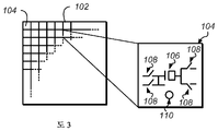
Figure 3 shows a representation of an embodiment of a passive device.
Figure 4 shows an enlarged view of an example of one possible embodiment of the structure.
Figure 5 shows an example representation of another possible embodiment of the structure.
Figure 6 shows a generic terminal footprint for the structure shown in Figure 5;
Figure 7 shows an exemplary representation of an embodiment of a structure having only capacitors and terminals.
Figure 8 shows a representation of an embodiment of a terminal footprint for an array using structures.
9 illustrates a side view representation of an embodiment of a package having a passive device, a power consumption device, and a memory device.
10 illustrates a side view representation of another embodiment of a semiconductor device package.
11 shows a side view representation of another embodiment of a semiconductor device package.
12 illustrates a side view representation of another embodiment of a package having a passive device, a power consumption device, and a memory device.
While the invention is susceptible to various modifications and alternative forms, specific embodiments thereof are shown by way of example in the drawings and will herein be described in detail. The drawings may not be drawn to scale. It should be understood that the drawings and detailed description thereto are not intended to limit the invention to the particular forms disclosed, but on the contrary, the intention is to cover all modifications, equivalents, and alternatives falling within the spirit and scope of the invention as defined by the appended claims. As the intent to cover them.
반도체 디바이스 패키지는 서로 결합된 2 이상의 반도체 디바이스를 포함할 수 있다. 소정 실시예들에서, 패키지 내의 반도체 디바이스들 중 적어도 하나는 수동 반도체 디바이스이고, 반도체 디바이스들 중 적어도 하나는 전력 소모 반도체 디바이스(예컨대, SOC 디바이스와 같은 전류 소모 소자들을 갖는 디바이스)이다. 수동 디바이스가 패키지 내에 집적됨에 따라, 수동 디바이스는 예를 들면, 집적된 수동 디바이스(integrated passive device; IPD)로 불릴 수 있다.A semiconductor device package may include two or more semiconductor devices coupled together. In some embodiments, at least one of the semiconductor devices in the package is a passive semiconductor device, and at least one of the semiconductor devices is a power consuming semiconductor device (e.g., a device having current dissipation elements such as SOC devices). As the passive device is integrated into the package, the passive device may be referred to as an integrated passive device (IPD), for example.
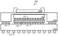
도 1은 반도체 디바이스 패키지(90)의 실시예의 분해도 표현을 도시한다. 도 2는 반도체 디바이스 패키지(90)의 실시예의 측면도 표현을 도시한다. 소정 실시예들에서, 패키지(90)는 수동 디바이스(100), 전력 소모 (반도체) 디바이스(120), 및 빌드업 패키지(build-up package)(122)를 포함한다. 일부 실시예들에서, 수동 디바이스(100), 전력 소모 디바이스(120), 및/또는 빌드업 패키지(122)는 유사한 기판들(예컨대, 실리콘계 기판들)을 사용한다. 수동 디바이스(100) 내에 유사한 기판들을 사용하여, 전압 소모 디바이스(120), 및/또는 빌드업 패키지(122)는 디바이스들 각각에 실질적으로 유사한 열 팽창 속성들을 제공하여, 이는 2개의 디바이스들 사이의 연결 시에 변형을 초래하지 않으면서 넓은 온도 범위에 걸친 동작을 허용할 수 있다. 소정 실시예들에서, 수동 디바이스(100)는 빌드업 패키지(122) 내의 리세스 내측에 정합하도록 크기설정된다. 수동 디바이스(100)는 전력 소모 디바이스 상의 영역이 전력 소모 디바이스를 위한 범용 I/O에 사용될 수동 다바이스에 의해 덮이지 않도록 전력 소모 디바이스(120)보다 작을 수 있다.1 illustrates an exploded view representation of an embodiment of a
소정 실시예들에서, 수동 디바이스(100) 및 전력 소모 디바이스(120)는 서로 직접 결합된다. 예를 들면, 디바이스들은 도 2에 도시된 바와 같이 단자들(110)을 사용하여 결합될 수 있다. 단자들(110)은 마주보는 범프들 또는 볼들, 관통 실리콘 비아(TSV), 또는 다른 3차원 상호접속 단자들과 같은 단자들일 수 있다. TSV 또는 다른 비아들은 예를 들면, 레이저 드릴링을 사용하여 빌드업 층 내에 형성될 수 있다. 소정 실시예들에서, 수동 디바이스(100) 상에 존재하는 소정 TSV는 패키지 또는 인쇄 기판 회로에 수동 디바이스를 통해 라우트-쓰루(route-through)들로만 사용된다. 디바이스들을 직접 결합하는 것은, 수동 디바이스 상의 소자들과 및 전력 소모 디바이스(120) 상의 조정기 소자들 및 전류 소모 소자들 사이에 단락 및 초고밀도 연결들을 제공할 수 있다.In certain embodiments, the
단자들(110)은 또한 전력 소모 디바이스(120) 및/또는 수동 디바이스(100)를 빌드업 패키지(122)에 직접 결합할 수 있다. 전력 소모 디바이스(120)와 빌드업 패키지(122) 사이에 결합된 단자들(110)은 범용 I/O 연결들에, 또는 집적된 조정기를 포함하지 않는 전력 연결들에 사용될 수 있다. 일부 실시예들에서, 빌드업 패키지(122)에 수동 디바이스(100)를 결합하는 소정 단자들은 전력 소모 디바이스(120)로부터 직접적으로 빌드업 패키지(122)까지의 라우트-쓰루(예컨대, 3차원 라우트-쓰루) 단자들이다. 도 2에 도시된 바와 같이, 빌드업 패키지(122)는 패키지 단자들(126)에의 라우팅(124)을 포함할 수 있다. 패키지 단자들(126)은 인쇄 회로 기판(PCB) 또는 다른 디바이스에 패키지(90)를 결합하는 데 사용될 수 있다.
전력 소모 디바이스(120)는 예를 들면, SOC 디바이스일 수 있다. 소정 실시예들에서, 수동 디바이스(100)는 하나 이상의 수동 소자(예컨대, 수동 구조체들 또는 수동 디바이스들)를 포함한다. 수동 소자들은 전력 소모 디바이스(120) 상의 소자들과 조합하여 사용되어 전력 소모 디바이스에 제공된 전압을 조절하고 조정할 수 있다.The power-consuming
도 3은 수동 디바이스(100)의 실시예의 표현을 도시한다. 소정 실시예들에서, 수동 디바이스(100)는 어레이(102)를 포함한다. 어레이(102)는 구조체들(104)(예컨대, 수동 구조체들)의 실질적으로 규칙적인 패턴(어레이)을 포함할 수 있다. 예를 들면, 도 3에 도시된 바와 같이, 어레이(102)는 타일형 패턴으로 배열된 구조체들(104)을 포함한다. 그러나, 구조체들(104)은 임의의 실질적으로 규칙적인 패턴으로 배열되어 수동 디바이스(100) 상에 어레이(102)를 형성할 수 있다. 일부 실시예들에서, 구조체들(104)은 반규칙적인 패턴(semiregular pattern)으로 배열되어 수동 디바이스(100) 상에 어레이(102)를 형성할 수 있다.FIG. 3 illustrates a representation of an embodiment of
소정 실시예들에서, 구조체들(104)은 커패시터들(예컨대, 트렌치 또는 다른 형태의 고밀도 커패시터들)과 같은, 그러나 이로 제한되지 않는 하나 이상의 수동 소자를 포함하는 규칙적인 구조체들이다. 구조체들(104)은 스위치들과 같은 다른 소자들을 포함할 수 있다. 도 4는 구조체(104)의 하나의 가능한 실시예의 예의 확대도를 도시한다. 도 4에 도시된 바와 같이, 구조체(104)는 커패시터(106) 및 4개의 스위치들(108)을 포함할 수 있다. 단자들(110)은 구조체(104) 내의 소자들(예컨대, 커패시터(106) 및/또는 스위치들(108))을 다른 구조체 또는 다른 반도체 디바이스에 결합하는 데 사용될 수 있다. 소정 실시예들에서, 어레이 구조체들(104)의 단자들에의 연결들은 국부적인 마주보는 범프 또는 TSV를 통해 어레이 구조체 바로 위에 또는 아래에 전력 소모 디바이스(120)의 영역에 직접 결합된다.In some embodiments, the
일부 실시예들에서, 구조체(104)는 수동 디바이스(100) 상에 규칙적인 패턴의 일부로서 제공될 수 있는 인덕터 또는 바이폴라 디바이스들과 같은 추가 소자들을 포함한다. 예를 들면, 추가 소자들은 어레이(102)에 걸쳐 제공될 수 있거나, 그것들이 어레이의 일부분(예컨대, I/O 주변 링에 사용되는 디바이스(104) 둘레의 링)에만 제공될 수 있고, 이는 이러한 구조체들은 소정 서브-기능들에 대해서만 요구될 수 있고 과도한 영역을 소모할 수 있기 때문이다.In some embodiments, the
일부 실시예들에서, 어레이(102)는 어레이 구조체들(104)의 소정 부분들 사이에 다른 저저항 결합들(예컨대, 전력 공급 레일들)을 포함한다. 저저항 결합은 수동 디바이스(100)에, 또는 예를 들면, TSV 연결의 양면 본질을 통해, 수동 디바이스의 배면에 결합될 수 있는 반도체 디바이스 내의 추가 디바이스나 라우팅 층에 제공될 수 있다. 저저항 결합은, 전력 소모 디바이스(120)의 라우팅 층들 상에 영향을 최소로 주면서, 전력 그리드 저항을 낮추고 수동 디바이스(100)의 프로그램 가능성 및/또는 가용성을 향상시키는 데 사용될 수 있다. 저저항 결합 상으로 전력을 이동시키는 것은, 전력 소모 디바이스로 하여금 전력 소모 디바이스와 수동 디바이스(100) 사이의 국부 전압 도메인들을 효과적으로 정의하게 할 수 있다.In some embodiments, the
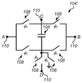
도 5는 어레이 소자 구조체(104')의 다른 가능한 실시예의 예의 표현을 도시한다. 도 6은 도 5에 도시된 구조체(104')를 위한 일반 단자 풋프린트를 도시한다. 도 5에 도시된 바와 같이, 구조체(104')는 일반 6-스위치 구성에 커패시터(106) 및 스위치들(108)을 포함할 수 있다. 구조체(104')는 전력 연결들에 사용되는 4개의 단자 및 게이트 제어에 사용되는 4개의 단자를 갖는 8개의 단자(110)(도 6에 도시됨)를 포함할 수 있다. 단자들(110)은 범프 또는 TSV일 수 있다. 하나 이상의 구조체(104')는 일반 레이아웃으로 배열될 수 있고, 구조체들을 사용하는 수동 디바이스는 단자들(110)을 통해 수동 디바이스에 결합되는 다른 반도체 디바이스(예컨대, 도 1 및 도 2에 도시된 전력 소모 디바이스(120))의 연결성을 사용하여 효과적으로 '프로그래밍'될 수 있다. 이러한 방식에서, 도 3에 도시된, 수동 디바이스(100)를 위한 동일한 설계가 상이한 전력 소모 디바이스들(120)에 의해 상이한 기능들에 사용될 수 있다.FIG. 5 illustrates an exemplary representation of another possible embodiment of the array element structure 104 '. FIG. 6 illustrates a generic terminal footprint for the structure 104 'shown in FIG. As shown in FIG. 5, the structure 104 'may include a
소정 실시예들에서, 도 3에 도시된, 수동 디바이스(100) 내의 스위치들(또는 다른 능동 소자들)의 수가 최소화된다. 예를 들면, 수동 디바이스(100)는 커패시터들(예컨대, 수동 소자들)만을 포함할 수 있거나, 수동 디바이스는 커패시터들, 및 단지 수 개의 스위치들 또는 전력 공급 레일들을 포함할 수 있다. 커패시터들 및 수 개의 스위치들은 어레이(102)로 구조체(104) 내에서 서로 결합되어, 어레이 입도(granularity)가 수동 디바이스(100)에 결합하는 데 사용되는 단자들(TSV, 범프, 또는 다른 연결)의 입도와 최대 일치할 때까지 어레이의 입도를 증가시킬 수 있다.In some embodiments, the number of switches (or other active elements) in the
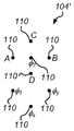
도 7은 커패시터들(106) 및 단자들(110)만을 갖는 수동 디바이스 구조체(104'')의 실시예의 다른 예의 표현을 도시한다. 소정 실시예들에서, 구조체(104'')(및 어레이(102))는 양의 단자들(110CAT)과 음의 단자들(110ANO) 사이에 최대 이격 거리를 갖고 레이아웃(예컨대, 설계)될 수 있다. 양의 단자들(110CAT) 및 음의 단자들(110ANO)을 주어진 전력 연결 밀도에 가능한 최대 거리로 분리하는 것은 커패시터들(106) 사이의 단락의 가능성을 최소화할 수 있다. 일부 실시예들에서, 양의 단자들(110CAT) 및 음의 단자들(110ANO)을 분리하는 것은 커패시터들(106) 사이의 단락을 실질적으로 금지한다. 단자들 사이의 오정렬은 어레이 내의 특정 셀에 대한 개방 고장(예컨대, "소프트" 고장) 또는 어레이 내의 2개의 셀들 사이의 단락을 갖는 구조체를 초래할 수 있다. 그러나, 개방 고장은 단지 폐루프 조정기에서 보상될 수 있는 커패시턴스의 작은 감소를 초래할 수 있는 반면, 단락 고장(단자들 사이의 거리가 너무 작아서 초래됨)은 수동 디바이스(100)의 수율 손실을 초래할 수 있다.Figure 7 illustrates another example representation of an embodiment of
도 8은 구조체(104'')(도 7에 도시됨)와 유사한 구조체들을 사용하는 어레이에 대한 단자 풋프린트(800)의 실시예의 표현을 도시한다. 도 8에 도시된 바와 같이, 어레이(102')는 단자들(110)의 2×2 그리드들을 포함하는, 9(아홉)개의 구조체들(104''')을 포함한다. 단자들(110)은 예를 들면, TSV 또는 범프일 수 있다. 각 구조체(104''')는, 라우트-쓰루("RT") 리소스들(예컨대, 3차원 라우팅된 리소스들), 수평 트랙("HT"), 또는 수직 트랙("VT")을 위한 단자들에 부가하여 구조체 내의 커패시터들의 캐소드들("CAT") 및 애노드들("ANO")을 위한 단자들을 포함한다.FIG. 8 shows a representation of an embodiment of a
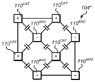
CAT 및 ANO 단자들은 각 구조체(104''')의 대향 코너들에 배치되어 단자들 사이의 단락 가능성을 감소시킬 수 있다. RT 단자들, HT 단자들, 및 VT 단자들은 x 방향 및 y 방향 둘 다로 어레이(102') 내의 구조체들(104''') 사이에서 교호적일 수 있다. HT 단자들 및 VT 단자들은 전력 레일로서 사용될 수 있는, 수평 트랙들 및/또는 수직 트랙들에의 연결이 제공될 수 있다. 수평 및 수직 트랙들은, 예를 들면, 하나 이상의 구조체에 전력을 연결하는 능력을 제공하는 수동 디바이스(100) 내의 금속 라우팅(레일들)(112)을 포함할 수 있다. HT 단자들 및 VT 단자들은 저저항 수평 트랙들 및 수직 트랙들이 전형적으로 커패시터 연결들보다 덜 자주 요구됨에 따라 더 적은 구조체들에 제공될 수 있다. 어레이(102') 내의 비음영 구조체들(104''')(예컨대, 중앙의 음영 구조체 외측의 구조체들)은 어레이가 x 방향 또는 y 방향으로 스테핑되는(stepped) 경우 어레이의 영역들이 중첩될 수 있다(예컨대, 영역들은 어레이(102')가 더 큰 어레이를 생성하도록 베이스 어레이로서 사용되는 경우 중첩할 수 있다).CAT and ANO terminals may be placed at opposite corners of each
수동 디바이스(100) 내에 스위치들이 없는 구조체(구조체(104'') 또는 구조체(104''')와 같음)를 사용하는 것은 스위칭 소자들 또는 다른 능동 소자들로 하여금 반도체 디바이스 패키지(예컨대, 패키지(90)) 내의 수동 디바이스에 결합되는 전력 소모 디바이스(예컨대, 도 1 및 도 2에 도시된 전력 소모 디바이스(120)) 상에 주로(또는 완전히) 위치되게 할 수 있다. 따라서, 수동 디바이스(100)를 형성하기 위한 프로세싱 기술은 더 양호한 커패시터들(예컨대, 가능한 한 이상적인 커패시터들에 근접한 커패시터들을 생성하는 것) 및/또는 인덕터들 또는 저저항 전력 공급 레일들과 같은 다른 수동 소자들을 생성하는 것에 집중될 수 있다. 다른 능동 소자들(전압 조정기의 컴포넌트들과 같음)과 조합하여 이러한 디바이스들을 생성하는 것 대신에 수동 디바이스들을 생성하는 것에 프로세싱 기술을 집중하는 것은 패키지(90) 내의 커패시터들에 대한 향상된 신뢰성 및 동작을 제공할 수 있다. 예를 들면, 커패시터들은 더 작은 등가직렬저항(ESR)을 갖고/갖거나 그들의 애노드 또는 캐소드 단자들로부터 접지에의 더 작은 기생 커패시턴스를 가질 수 있다. 또한, 스위치들은 전형적으로 스위치들을 생성하기 위한 양호한 기술을 갖는, 전력 소모 디바이스(120)로 주로 이동된다. 일부 실시예들에서, 수동 디바이스(100)는 전력 소모 디바이스(120)와 상당히 상이한 공정을 사용하여 개발되는 스위치들 또는 다른 컴포넌트들을 또한 포함할 수 있다. 예를 들면, 질화 갈륨(GaN) 공정은 더 높은 전도도를 지원하고 더 높은 전압들을 견디도록 사용될 수 있다. 수동 디바이스(100)에 대한 이러한 공정 최적화는 전력 소모 디바이스(120)를 위한 공정의 최적화가 독립적으로 이루어질 수 있다.Using structures (such as structure 104 '' or structure 104 '' ') without switches in
전력 소모 디바이스(120)는 통상의 규칙적인 SOC 디바이스의 소자들을 포함할 수 있다. 소정 실시예들에서, 전력 소모 디바이스(120)는 도 1 및 도 2에 도시된 바와 같이 수동 디바이스(100)에 결합되어, 수동 디바이스 상에 소자들(예컨대, 커패시터들)을 위한 단자들의 그리드(예컨대, 어레이)를 이용하여 전력 소모 디바이스가 조정기들 사이에 미세 입도를 갖는 별개의(예컨대, 분리되고 국부화된) 전압 조정기들을 생성하게 한다. 별개의 전압 조정기들은 구조체들의 그룹들보다 높은 입력 전압이 제공될 수 있거나 전력 소모 디바이스(120) 상의 소자들(예컨대, IP 블록들과 같은 블록들)이 요구될 수 있고/있거나 직접적으로 견딜 수 있다. 별개의 전압 조정기들은, 전압 조정기들을 분리하고 국부화는 것이 패키지 연결 리소스들을 사용하지 않으면서 각 전압 조정기가 자신의 대응하는 블록(예컨대, 선택된 블록)에 직접적으로 원하는 입력 전압을 제공하게 하기 때문에 더 높은 입력 전압에서 동작할 수 있다.The
마주보는 범프들 또는 볼들을 단자들로서 사용하는 실시예들에서(예컨대, TSV는 수동 디바이스(100)를 통해 사용되지 않음), 높은 입력 전압들은 수동 디바이스를 거치지 않으면서 전력 소모 디바이스(120)에 제공될 필요가 있을 수 있다(예컨대, 높은 입력 전압들을 위한 단자들은 수동 디바이스에 의해 덮이는 영역 외측에 위치되어야 한다). 예를 들면, 도 2에 도시된 실시예에 대하여, 수동 디바이스(100) 및 전력 소모 디바이스(120)에 직접 연결하는 단자들(110)은 마주보는 범프들 또는 볼들일 수 있고, 따라서 수동 디바이스의 에지들의 외측의 단자들(예컨대, 단자들(110B))은 높은 입력 전압들을 위한 단자들로서 사용될 수 있다. 그러나, 이러한 높은 입력 전압은 수동 디바이스(100)가 없는 패키지들보다 낮은 전류에서 제공될 수 있는데, 그 이유는 수동 디바이스(100) 및 전력 소모 디바이스(120)로부터의 소자들의 조합하여 내장된 별개의 전압 조정기들은 전압의 국부화된 감소를 전력 소모 디바이스(120) 상의 블록들에 순응하는 레벨까지 허용하기 때문이다. 전력 = 전압*전류이므로, 더 높은 전압들(예컨대, 전력 소모 디바이스(120) 상의 블록들에 사용되는 전압들보다 3 내지 8배 높음)을 제공하는 것은, 전력 소모 디바이스에서 동일한 전력 레벨을 달성하도록 제공되는 더 적은 전류를 허용하고, 따라서 더 적은 단자들(예컨대, 범프들 또는 볼들)이 패키지에 전력 및 접지를 제공하는 데 사용될 수 있다.In embodiments where opposing bumps or balls are used as terminals (e.g., TSV is not used through passive device 100), high input voltages are provided to
별개의 전압 조정기들은 단일 또는 멀티-레벨 스위치형-캡 변환기(multi-level switched-cap converter), 벅 변환기(buck converter), 또는 하이브리드 변환기들(예컨대, 벅 및 스위치형-캡 변환기 둘 다의 조합)을 포함하지만 이로 제한되지 않는 상이한 유형의 전압 조정기들로서 설계될 수 있다. 하이브리드 또는 벅 변환기들은 수동 디바이스(100) 또는 전력 소모 디바이스(120) 상에서 인덕터들의 사용을 필요로 할 수 있다.The separate voltage regulators may be implemented as single or multi-level switched-cap converters, buck converters, or hybrid converters (e.g., a combination of both buck and switched- , ≪ / RTI > but not limited to, voltage regulators of different types. Hybrid or buck converters may require the use of inductors on the
전력 소모 디바이스(120)는 수동 디바이스(100) 상의 어레이(예컨대, 어레이(102'))를 이용하여 어레이(및 구조체들(104'') 또는 구조체들(104''')과 같은 어레이의 구조체들의 서브세트)를 전력 소모 디바이스를 위한 전압 조정기들을 생성하는 데 필요한 속성들에 매핑함으로써 별개의 국부화된 전압 조정기들을 생성한다. 어레이는 로직, 연결성, 또는 전력 소모 디바이스(120) 상의 임의의 구조체들을 사용함으로써 매핑되어, 수동 디바이스(100) 상의 구조체들이나 소자들과 전력 소모 디바이스 상의 블록들 사이의 연결성을 '프로그래밍'하거나 결정할 수 있다. 따라서, 전력 소모 디바이스(120)는 전력 소모 디바이스 상의 대응하는 블록의 필요성에 따라, 어떤 속성들이 각 전압 조정기에 필요한지를 결정할 수 있다(예컨대, 덮이고 연결된 영역들, 전압 분할비, 동작 주파수, 피드백 포인트, 인에이블 제어 등).The power-consuming
소정 실시예들에서, 전력 소모 디바이스(120) 상의 선택된 블록과 조합하여 사용되는 수동 디바이스(100) 상의 구조체들은 선택된 블록에서 또는 그 근처에서 영역 내에 국부화된다. 예를 들면, 선택된 블록과 조합하여 사용되는 수동 디바이스(100) 상의 구조체들은 수동 디바이스가 전력 소모 디바이스(120)에 대하여 수직으로 적층되는 경우 선택된 블록 바로 아래에 또는 바로 위에 있을 수 있다. 전력 소모 디바이스(120) 상의 선택된 블록과 조합하여 사용되는 수동 디바이스(100) 상의 구조체들을 국부화하는 것은, 전압 조정기와 전압 조정기에 의해 전력이 제공되는 선택된 블록 사이의 거리를 줄인다(또는 최소화한다). 전압 조정기와 선택된 블록 사이의 거리를 감소시키는 것, 및 (3D 연결성의 경우에, 선택된 블록 위의 단자들의 어레이에 의해 크게 정의되는) 연결된 임피던스를 줄이는 것은, 선택된 블록이 겪는 전압 I*R 강하를 줄이거나 최소화하고 선택된 블록에 전력 분배의 효율성을 향상시킬 수 있다. 거리를 줄이는 것은, 또한 공급된 전압의 매우 신속한 국부 피드백을 전압 조정 루프에 제공함으로써(예컨대, 전압 마진 요건들을 최소화하고 피드백 시간을 줄이는, 높게 국부화된 피드백 응답), TSV 또는 범프 연결성을 사용하여 더 낮은 저항을 제공함으로써, 그리고 더 높은 전류, 더 낮은 전압 경로를 위한 더 짧은 거리(예컨대, 소량 내지 없는 보드 트레이스)를 제공함으로써, 전압 강하를 줄일 수 있다. 또한, 전압 I*R 강하를 선택된 블록까지 줄이는 것은 증가될 디바이스의 최대 동작 주파수 또는 감소될 최소 동작 전압을 허용할 수 있다. 선택된 블록들을 위한 동작 주파수 또는 동작 전압은 활성 피드백 제어를 사용하여 증가되어 전력 소모 디바이스(120)에서 에이징 효과(aging effects)를 줄일 수 있다.In some embodiments, the structures on the
소정 실시예들에서, 별개의 전압 조정기들을 분리하고 국부화하는 것은 선택된 블록을 위한 입력 전압이 원하는 동작 주파수를 위한 최소 동작 포인트로 감소되게 한다. 따라서, 별도의 DVFS(dynamic voltage & frequency scaling) 설정 및 전원 차단 기능들은 전력 소모 디바이스(120) 내의 다른 블록들에 영향을 주지 않으면서 개별 블록에 제공될 수 있다. 이러한 경우들에서, 레벨 변환기들은 상이한 DVFS 전압 도메인들에서 동작하는 블록들 사이의 연결들이 요구될 수 있다. 또한, 별개의 전압 조정기들을 사용하는 것은 상대적으로 높은 전력 블록이 속도 제한 중요 경로를 갖는 블록으로부터 상이한 전력 공급 전압을 이용하게 하고 PMU로부터 가장 멀 수 있다. 별개의 전압 조정기들 없이, 높은 전력 블록 및 속도 제한 중요 경로를 갖는 블록은 전압 공급을 공유해야만 할 수 있고, 따라서 높은 전력 블록에 공급되는 전압은 속도 제한 중요 경로를 갖는 블록에서 성능을 유지하기 위하여 최소 레벨에서 유지되어야만 하고, 따라서 동일한 중요 경로를 포함할 수 없는 높은 전력 블록에서 전력을 낭비한다. 높은 전력 블록의 전압 조정을 속도 제한 중요 경로를 갖는 블록의 전압 조정으로부터 분리하는 것은, 속도 제한 중요 경로를 갖는 블록의 성능에 영향을 주지 않으면서 높은 전력 블록에 제공된 전력이 그 자신의 중요 경로를 최적화되게 한다(예컨대 전압을 감소시킴으로써). 동작의 모드들 또는 다른 조건들에 따라, 상이한 블록들은 상당히 상이한 중요 경로들 및 전력 소모를 가질 수 있고, 이는 최적화 전력 소모에는 좋지 않은 생각으로 이러한 블록들 사이에서 전압 공급들의 공유를 할 수 있게 한다.In certain embodiments, isolating and localizing the separate voltage regulators causes the input voltage for the selected block to be reduced to a minimum operating point for the desired operating frequency. Therefore, separate dynamic voltage & frequency scaling (DVFS) setup and power down functions can be provided to the individual blocks without affecting other blocks within the
일부 실시예들에서, 전력 소모 디바이스(120) 내의 블록들의 서브-부분들(예컨대, CPU 또는 FPU 내에서 ALU 또는 MPY와 같은 별도의 기능)은 그 자신의 전압 조정기들로부터 동작할 수 있다. 예를 들면, 전력 소모 디바이스(120)는 전력 소모 디바이스 내의 블록들의 서브-부분들에 대해 국부화되고 별개인 수동 디바이스(100)를 사용하여 전압 조정기들을 정의할 수 있다. 서브-부분들에 대해 전압 조정을 분리하고 국부화하는 것은 상이한 서브-부분들에 의해 제어된 각 기능에 대해 전압의 최적화를 허용한다. 따라서, 원하는 동작 주파수에서 전력 소모는 심지어 더 최소화될 수 있다. 전압의 이러한 중요 경로 최적화(예컨대, 서브-부분 기능에 기초한 최적화)는 예를 들면 매칭 경로, 룩업 테이블, 경로 상의 검출기로서 초기/후기 중복 플롭(redundant flop), 또는 다른 유사한 방법을 사용하여 행해질 수 있다.In some embodiments, the sub-portions of the blocks within the power consumption device 120 (e.g., separate functions such as ALU or MPY within the CPU or FPU) may operate from their own voltage regulators. For example,
일부 실시예들에서, 하나 이상의 별개의 전압 조정기 또는 조정기들의 소정 서브-컴포넌트들은 저전력 누설을 금지하기 위해 전력-게이팅 디바이스로서 기능하고 필수적으로 전력 소모 디바이스들 상의 누설을 감소시키는 데 사용되는 기존 전력-게이팅 디바이스들을 대체한다. 예를 들면, 전력 소모 디바이스(120) 상의 선택된 블록이 전원 차단되는 경우, 별개의 전압 조정기 내의 하나 이상의 스위치(예컨대, 전압 조정기의 스위치형-캡 구현)는 차단될 수 있다. 스위치들을 차단하는 것은 전력 소모 디바이스(120) 내에 현재 포함되는, 추가 전력-게이팅 디바이스들을 필요로 하지 않으면서 활성 블록 내의 누설을 감소시킬 수 있다.In some embodiments, one or more of the separate voltage regulators or certain sub-components of the regulators may function as a power-gating device to inhibit low-power leakage and may be used to power a conventional power- Replacing gating devices. For example, when a selected block on the power-consuming
일부 실시예들에서, 인접한 별개의 전압 조정기들은 전력 소모 디바이스(120) 상의 블록들의 필요에 따라 수동 디바이스(100) 상의 리소스들을 공유할 수 있다. 예를 들면, 전력 소모 디바이스(120) 상의 소정 기능들은 동시에 동작하지 않는 것으로 알려졌다. 이러한 실시예들에서, 수동 디바이스(120) 상의 구조체들 또는 소자들의 부분들(예컨대, 수동 디바이스 상의 커패시터들 또는 타일들)은, 행 또는 열 연결들을 계속하여 예를 들면, 스위치들을 통해 공유된 디바이스들을 행 또는 열 내의 공통 레일에 포함함으로써 하나의 별개의 전압 조정기 또는 다른 전압 조정기에 교호적으로 할당될 수 있다.In some embodiments, adjacent separate voltage regulators may share resources on the
소정 실시예들에서, 수동 디바이스(100)는 일반적인 구조체들의 규칙적인 어레이를 포함한다(예를 들면, 수동 디바이스는 전력 소모 구조체들의 2개 이상의 상이한 설계와 함께 사용될 수 있다). 일반 수동 디바이스를 사용하여 생성된 별개의 전압 조정기들의 속성들은 일반 수동 디바이스에 결합되는 전력 소모 디바이스에 의해 제어될 수 있다. 예를 들면, 전압 조정기들을 위한 입도 선택들(예컨대, 국부화된 패턴들), 제어, 및 구동 회로는 전력 소모 디바이스 상에 배치될 수 있다. 따라서, 일반 수동 디바이스는 일반 수동 디바이스의 설계를 수정하지 않으면서 여러 상이한 전력 소모 디바이스와 함께 또는 유사한 전력 소모 디바이스들의 여러 상이한 세대에 걸쳐 사용될 수 있다. 예를 들면, 도 8에 도시된, 풋프린트(800)는 많은 상이한 전력 소모 디바이스들(심지어 상이한 제조업자들로부터의 전력 소모 디바이스들)과 함께 사용되는 일반 수동 디바이스를 생성하는 데 사용될 수 있고/있거나 일반 수동 디바이스는 일반 수동 디바이스 연결들의 동일한 일반 명세 또는 "풋프린트"에 상이한 제조업자에 의해 제조될 수 있다. 일반 수동 디바이스 설계를 제공하는 것은, 일반 수동 디바이스가 여러 플랫폼 및/또는 디바이스들의 세대에 걸쳐 사용가능한 상품으로서 생산될 수 있으므로, 일반 수동 디바이스의 설계 및/또는 제조가 최적화되게 하고 일반 수동 디바이스를 생성하기 위한 비용이 감소되게 한다.In some embodiments, the
일부 실시예들에서, 반도체 디바이스 패키지는 수동 디바이스(100) 및 전력 소모 디바이스(120)에 부가하여 하나 이상의 추가 디바이스를 포함한다. 예를 들면, 반도체 디바이스 패키지는 수동 디바이스(100) 및 전력 소모 디바이스(120)에 부가하여 메모리 디바이스(예컨대, 고속 또는 저전력 DRAM 코어와 같은 DRAM 디바이스)를 포함할 수 있다. 도 9는 수동 디바이스(100), 전력 소모 디바이스(120), 및 메모리 디바이스(250)를 구비한 패키지(200)의 실시예의 측면도 표현을 도시한다. 패키지(200)는 상부 빌드업 패키지(122A) 및 하부 빌드업 패키지(122B)를 포함할 수 있다.In some embodiments, the semiconductor device package includes one or more additional devices in addition to the
메모리 디바이스(250)는 수동 디바이스(100) 및 전력 소모 디바이스(120)가 상부 패키지(122A)와 하부 패키지(122B) 사이에 서로 결합되고 샌드위치되는 동안 상부 패키지에 결합될 수 있다. 소정 실시예들에서, 수동 디바이스(100) 및 전력 소모 디바이스(120)는 상부 패키지(122A)의 리세스 내에 놓인다. 도 9에 도시된 바와 같이, 수동 디바이스(100) 및 전력 소모 디바이스(120)는 대략 동일한 크기일 수 있다. 따라서, 수동 디바이스(100)는 하부 패키지(122B)와 전력 소모 디바이스(120) 사이에 일반적인 I/O 연결들을 제공하기 위해 라우트-쓰루 단자들(예컨대, TSV)을 포함할 수 있다. 일부 실시예들에서, 수동 디바이스(100)는 전력 소모 디바이스(120)보다 작고 연결들은 앞서 설명한 바와 같이 수동 디바이스(100)에 의해 중첩되는 영역 외측의 전력 소모 디바이스에 제공된다.The
일부 실시예들에서, 수동 디바이스(100)는 수동 디바이스들의 어레이에 부가하여 수동 디바이스 내에 하나 이상의 다른 구조체를 포함한다. 예를 들면, 수동 디바이스(100)는 메모리 디바이스(250) 또는 다른 구조체들과 같은 구조체들을 포함할 수 있다. 도 10은 수동 디바이스(100) 내에 집적된 메모리 디바이스(250)를 갖는 패키지(90')의 실시예의 측면도 표현을 도시한다. 도 11은 수동 디바이스(100) 내에 집적된 메모리 디바이스(250)를 갖는 패키지(200')의 실시예의 측면도 표현을 도시한다. 수동 소자들(예컨대, 커패시터들)은 메모리 디바이스(250)를 형성하는 데 사용되는 공정 동안 제조될 수 있다. 일부 실시예들에서, 메모리 디바이스(250)를 형성하기 위한 공정은 수동 소자들을 형성하는 것을 포함하도록 약간 수정된다.In some embodiments, the
수동 디바이스(100)는 도 10 및 도 11에 도시된 바와 같이 전력 소모 디바이스(120)에 상대적으로 근접하여 위치되므로, 수동 디바이스는 전력 소모 디바이스와의 고도의 연결성을 갖는다. 따라서, 수동 디바이스(100)는 마주보는 범프 연결들, 또는 본 명세서에서 논의된 다른 패키징 연결들을 사용하여 수동 디바이스 내의 다른 구조체(예컨대, 메모리 디바이스(250))들에 높은 대역폭이며 저전력인 연결들을 제공할 수 있다. 도 10 및 도 11에 도시된, 패키지(90') 및 패키지(200')의 실시예들이 수동 디바이스(100) 내측에 메모리 디바이스(250)를 가지므로, 이러한 실시예들은, 메모리 디바이스와 전력 소모 디바이스(120) 사이에 높은 대역폭이며 저전력인 메모리 연결들, 및 수동 디바이스들이 본 명세서에서 설명한 다양한 상이한 조정기 구조체들(예컨대, 별개의 전압 조정기들)로 조합되는 경우 공급 필터링 또는 전력 조정을 위한 수동 디바이스 둘 다를 공급할 수 있다.Since the
일부 실시예들에서, 조정기 구조체들은 수동 디바이스(100) 내에 완전히 포함된다. 다른 실시예들에서, 조정기 구조체들의 부분들은 전력 소모 디바이스(120) 상에 위치된다. 소정 실시예들에서, 도 10에 도시된 바와 같이, 수동 디바이스(100)(및 메모리 디바이스(250))는 전력 소모 디바이스(120)보다 작다. 일부 실시예들에서, 수동 디바이스(100)는 전력 소모 디바이스(120)보다 실질적으로 더 작다. 수동 디바이스(100)는 전력 소모 디바이스(120)보다 작은 경우, 전력 소모 디바이스의 범프 영역의 일부분은 I/O 또는 다른 전력 전달 연결들에 이용가능하다. 일부 실시예들에서, 도 11에 도시된 바와 같이, 수동 디바이스(100)(메모리 디바이스(250)를 가짐)는 전력 소모 디바이스(120)와 크기가 실질적으로 유사하다.In some embodiments, regulator structures are fully contained within the
도 12는 TSV를 포함하는 수동 디바이스(100), 전력 소모 디바이스(120), 및 메모리 디바이스(250)를 구비한 패키지(200'')의 실시예의 측면도 표현을 도시한다. 패키지(200'')는 빌드업 패키지(122)와 전력 소모 디바이스(120) 사이에 샌드위치된 수동 디바이스(100) 및 메모리 디바이스(250)를 포함할 수 있다. 수동 디바이스(100)는 전력 소모 디바이스(120)와 메모리 디바이스(250) 사이에 연결들을 제공하기 위한 라우트-쓰루 단자들을 포함할 수 있다. 일부 실시예들에서, 수동 디바이스(100)는 전력 소모 디바이스(120)와 빌드업 패키지(122) 사이에 직접적인 일반의 I/O 연결들을 허용하도록 전력 소모 디바이스(120)로부터 오프셋된다. 일부 실시예들에서, 빌드업 패키지(122)는 수동 디바이스(100)를 거치지 않으면서 전력 소모 디바이스(120)와 메모리 디바이스(250) 사이의 연결을 위한 라우팅을 포함할 수 있다. 일부 실시예들에서, TSV는 수동 디바이스(100), 또는, 대안적으로, 전력 소모 디바이스(120), 또는 디바이스들 둘 다에 내장된다. 일부 실시예들에서, 메모리 디바이스(250) 및 수동 디바이스(100)의 기능들은 단일 다이 상에 있도록 조합된다. 이는 메모리 디바이스가 자신의 근본적인 공정의 일부로서 고밀도 커패시터 어레이를 포함하는 DRAM인 경우 특히 유용할 수 있다. 다이 기능의 다른 조합들은 가능하며 본 발명이 속한 기술분야에서 통상의 지식을 가진 자에게 명백할 것이다.12 depicts a side view representation of an embodiment of a
일부 실시예들에서, 빌드업 재료, 스태거링(staggering), 및 마주하는 연결성의 사용과 같은 표준 패키지 기술들은 시스템 요건들과 조합되고, 시스템 내의 상이한 디바이스들로부터 TSV을 제거함으로써 비용을 절감하도록 통상의 기술자들에 의해 적용될 수 있다.In some embodiments, standard package technologies, such as the use of build-up materials, staggering, and facing connectivity, are combined with system requirements to reduce cost by removing TSVs from different devices in the system And can be applied by ordinary artisans.
본 발명의 다양한 양태들의 추가의 수정 및 대안적인 실시예들은 본 명세서의 관점에서 통상의 기술자들에게 명백할 것이다. 따라서, 이러한 설명은 예시적인 것으로서만 이해되며, 본 발명을 수행하는 일반적인 방식을 통상의 기술자들에게 교시하는 목적을 위한 것이다. 본 명세서에 도시되고 설명된 본 발명의 형태들은 현재 바람직한 실시예들로서 취해지는 것으로 이해되어야 한다. 요소들 및 재료들은 본 명세서에서 예시되고 설명되는 것을 대신할 수 있고, 부품들 및 공정들은 역으로 될 수 있으며, 본 발명의 소정 특징들은 본 발명의 이러한 설명의 이점을 가지므로 통상의 기술자들에게 명백함으로, 독립적으로 모두 이용될 수 있다. 이하 청구범위에 설명된 바와 같이 본 발명의 기술적 사상 및 범주를 벗어나지 않으면서 본 명세서에서 설명된 요소들의 변형이 이루어질 수 있다.Additional modifications and alternative embodiments of various aspects of the present invention will be apparent to those of ordinary skill in the art in view of this disclosure. Accordingly, this description is to be construed as exemplary only, and is for the purpose of teaching those of ordinary skill in the art the general manner of carrying out the invention. It is to be understood that the forms of the invention shown and described herein are taken as presently preferred embodiments. Elements and materials may be substituted for what is illustrated and described herein, and parts and processes may be reversed, and certain features of the present invention may have the benefit of this description of the invention, Obviously, they can all be used independently. Modifications of the elements described herein may be made without departing from the spirit and scope of the invention as set forth in the following claims.
Claims (15)
반도체 기판;
상기 반도체 기판 상에 형성된 복수의 수동 소자 - 상기 수동 소자들은 상기 반도체 기판 상에 어레이로 배열됨 -; 및
상기 수동 소자들을 적어도 하나의 추가 반도체 디바이스에 결합하기 위한 하나 이상의 단자
를 포함하는, 반도체 디바이스.1. A semiconductor device comprising:
A semiconductor substrate;
A plurality of passive elements formed on the semiconductor substrate, the passive elements arranged in an array on the semiconductor substrate; And
One or more terminals for coupling the passive elements to at least one additional semiconductor device
.
제1 반도체 디바이스 - 상기 제1 반도체 디바이스는,
제1 반도체 기판;
상기 제1 반도체 기판 상에 형성된 하나 이상의 수동 소자; 및
하나 이상의 단자를 포함함 -; 및
상기 단자들 중 하나 이상을 사용하여 상기 제1 반도체 디바이스에 결합되는 제2 반도체 디바이스 - 상기 제2 반도체 디바이스는,
제2 반도체 기판; 및
상기 제2 반도체 기판 상에 형성된 하나 이상의 전류 소모 소자를 포함함 ―
를 포함하는, 반도체 디바이스 패키지.A semiconductor device package,
A first semiconductor device, wherein the first semiconductor device comprises:
A first semiconductor substrate;
At least one passive element formed on the first semiconductor substrate; And
Comprising at least one terminal; And
A second semiconductor device coupled to the first semiconductor device using one or more of the terminals,
A second semiconductor substrate; And
And one or more current dissipation elements formed on the second semiconductor substrate,
≪ / RTI >
Applications Claiming Priority (5)
| Application Number | Priority Date | Filing Date | Title |
|---|---|---|---|
| US201361864014P | 2013-08-09 | 2013-08-09 | |
| US61/864,014 | 2013-08-09 | ||
| US14/077,512 | 2013-11-12 | ||
| US14/077,512 US9595526B2 (en) | 2013-08-09 | 2013-11-12 | Multi-die fine grain integrated voltage regulation |
| PCT/US2014/048603 WO2015020836A2 (en) | 2013-08-09 | 2014-07-29 | Multi-die fine grain integrated voltage regulation |
Publications (2)
| Publication Number | Publication Date |
|---|---|
| KR20160041969A true KR20160041969A (en) | 2016-04-18 |
| KR101819838B1 KR101819838B1 (en) | 2018-01-17 |
Family
ID=52447943
Family Applications (1)
| Application Number | Title | Priority Date | Filing Date |
|---|---|---|---|
| KR1020167005750A KR101819838B1 (en) | 2013-08-09 | 2014-07-29 | Multi-die fine grain integrated voltage regulation |
Country Status (8)
| Country | Link |
|---|---|
| US (5) | US9595526B2 (en) |
| EP (2) | EP3031081A2 (en) |
| JP (1) | JP6174260B2 (en) |
| KR (1) | KR101819838B1 (en) |
| CN (1) | CN105474391B (en) |
| DE (1) | DE202014011574U1 (en) |
| TW (1) | TWI529875B (en) |
| WO (1) | WO2015020836A2 (en) |
Families Citing this family (20)
| Publication number | Priority date | Publication date | Assignee | Title |
|---|---|---|---|---|
| US9595526B2 (en) | 2013-08-09 | 2017-03-14 | Apple Inc. | Multi-die fine grain integrated voltage regulation |
| US10468381B2 (en) | 2014-09-29 | 2019-11-05 | Apple Inc. | Wafer level integration of passive devices |
| US9971970B1 (en) | 2015-04-27 | 2018-05-15 | Rigetti & Co, Inc. | Microwave integrated quantum circuits with VIAS and methods for making the same |
| US9935076B1 (en) | 2015-09-30 | 2018-04-03 | Apple Inc. | Structure and method for fabricating a computing system with an integrated voltage regulator module |
| JP2017084961A (en) * | 2015-10-28 | 2017-05-18 | 株式会社村田製作所 | Mounting structure of integrated circuit element |
| US10665579B2 (en) | 2016-02-16 | 2020-05-26 | Xilinx, Inc. | Chip package assembly with power management integrated circuit and integrated circuit die |
| CN107369678A (en) * | 2016-05-13 | 2017-11-21 | 北京中电网信息技术有限公司 | A kind of system-in-a-package method and its encapsulation unit |
| US11121301B1 (en) | 2017-06-19 | 2021-09-14 | Rigetti & Co, Inc. | Microwave integrated quantum circuits with cap wafers and their methods of manufacture |
| US20190013301A1 (en) * | 2017-07-04 | 2019-01-10 | Intel Corporation | Stacked dies with passive components within facing recesses |
| US10529407B2 (en) * | 2017-07-20 | 2020-01-07 | Samsung Electronics Co., Ltd. | Memory device including a plurality of power rails and method of operating the same |
| US10535394B2 (en) * | 2017-07-20 | 2020-01-14 | Samsung Electronics Co., Ltd. | Memory device including dynamic voltage and frequency scaling switch and method of operating the same |
| DE102017129611B4 (en) * | 2017-12-12 | 2021-04-22 | RF360 Europe GmbH | Electrical device with two or more chip components |
| KR20200030411A (en) | 2018-09-12 | 2020-03-20 | 엘지이노텍 주식회사 | Flexible circuit board and chip pakage comprising the same, and electronic device comprising the same |
| US10756622B2 (en) | 2018-12-24 | 2020-08-25 | Apple Inc | Power management system switched capacitor voltage regulator with integrated passive device |
| DE102019110716B3 (en) * | 2019-04-25 | 2020-01-16 | Semikron Elektronik Gmbh & Co. Kg | Power semiconductor module with power semiconductor switches |
| US20200373224A1 (en) * | 2019-05-21 | 2020-11-26 | Microsoft Technology Licensing, Llc | Through-silicon vias and decoupling capacitance |
| US11710726B2 (en) | 2019-06-25 | 2023-07-25 | Microsoft Technology Licensing, Llc | Through-board power control arrangements for integrated circuit devices |
| KR20210017054A (en) | 2019-08-06 | 2021-02-17 | 삼성전자주식회사 | Multi-core system and controlling operation of the same |
| US11537154B2 (en) | 2020-12-09 | 2022-12-27 | Samsung Electronics Co., Ltd. | Mobile devices and methods controlling power in mobile devices |
| US20220367430A1 (en) * | 2021-05-17 | 2022-11-17 | Mediatek Inc. | Semiconductor package structure |
Family Cites Families (37)
| Publication number | Priority date | Publication date | Assignee | Title |
|---|---|---|---|---|
| US4080590A (en) * | 1976-03-31 | 1978-03-21 | International Business Machines Corporation | Capacitor storage memory |
| US5786979A (en) * | 1995-12-18 | 1998-07-28 | Douglass; Barry G. | High density inter-chip connections by electromagnetic coupling |
| WO2000079592A1 (en) * | 1999-06-17 | 2000-12-28 | Hitachi, Ltd. | Semiconductor device and electronic device |
| US6532143B2 (en) * | 2000-12-29 | 2003-03-11 | Intel Corporation | Multiple tier array capacitor |
| US6477034B1 (en) * | 2001-10-03 | 2002-11-05 | Intel Corporation | Interposer substrate with low inductance capacitive paths |
| US7327554B2 (en) * | 2003-03-19 | 2008-02-05 | Ngk Spark Plug Co., Ltd. | Assembly of semiconductor device, interposer and substrate |
| US7190210B2 (en) * | 2004-03-25 | 2007-03-13 | Integral Wave Technologies, Inc. | Switched-capacitor power supply system and method |
| US7446389B2 (en) * | 2004-06-17 | 2008-11-04 | Apple Inc. | Semiconductor die package with internal bypass capacitors |
| WO2006114772A1 (en) | 2005-04-28 | 2006-11-02 | Nxp B.V. | Integrated circuit assembly with passive integration substrate for power and ground line routing on top of an integrated circuit chip |
| JP4546415B2 (en) * | 2005-09-01 | 2010-09-15 | 日本特殊陶業株式会社 | Wiring board, ceramic capacitor |
| US7692284B2 (en) * | 2005-12-12 | 2010-04-06 | Intel Corporation | Package using array capacitor core |
| US7612984B2 (en) * | 2006-11-01 | 2009-11-03 | Taiwan Semiconductor Manufacturing Company, Ltd. | Layout for capacitor pair with high capacitance matching |
| US20080128854A1 (en) * | 2006-12-04 | 2008-06-05 | Augustine Anne E | Embedded array capacitor with top and bottom exterior surface metallization |
| US8264846B2 (en) * | 2006-12-14 | 2012-09-11 | Intel Corporation | Ceramic package substrate with recessed device |
| US20080157343A1 (en) | 2006-12-29 | 2008-07-03 | Sriram Dattaguru | Ceramic interposer with silicon voltage regulator and array capacitor combination for integrated circuit packages |
| JP4734282B2 (en) * | 2007-04-23 | 2011-07-27 | 株式会社日立製作所 | Semiconductor chip and semiconductor device |
| EP2147499B1 (en) * | 2007-05-10 | 2016-08-17 | Nxp B.V. | Dc-to-dc converter comprising a reconfigurable capacitor unit |
| US8476735B2 (en) * | 2007-05-29 | 2013-07-02 | Taiwan Semiconductor Manufacturing Company, Ltd. | Programmable semiconductor interposer for electronic package and method of forming |
| JP4429346B2 (en) * | 2007-08-31 | 2010-03-10 | 富士通株式会社 | Semiconductor device and manufacturing method thereof |
| US7952160B2 (en) | 2007-12-31 | 2011-05-31 | Intel Corporation | Packaged voltage regulator and inductor array |
| US8341434B2 (en) | 2008-02-26 | 2012-12-25 | International Business Machines Corporation | Optimizing voltage on a power plane using a networked voltage regulation module array |
| US20100165585A1 (en) | 2008-12-26 | 2010-07-01 | Megica Corporation | Chip packages with power management integrated circuits and related techniques |
| US8242551B2 (en) * | 2009-03-04 | 2012-08-14 | Taiwan Semiconductor Manufacturing Company, Ltd. | Metal-insulator-metal structure for system-on-chip technology |
| US9607935B2 (en) * | 2009-04-21 | 2017-03-28 | Ati Technologies Ulc | Semiconductor chip package with undermount passive devices |
| US8188786B2 (en) * | 2009-09-24 | 2012-05-29 | International Business Machines Corporation | Modularized three-dimensional capacitor array |
| US8558345B2 (en) * | 2009-11-09 | 2013-10-15 | International Business Machines Corporation | Integrated decoupling capacitor employing conductive through-substrate vias |
| US9048112B2 (en) | 2010-06-29 | 2015-06-02 | Qualcomm Incorporated | Integrated voltage regulator with embedded passive device(s) for a stacked IC |
| US9064712B2 (en) * | 2010-08-12 | 2015-06-23 | Freescale Semiconductor Inc. | Monolithic microwave integrated circuit |
| US8716855B2 (en) | 2010-11-10 | 2014-05-06 | Taiwan Semiconductor Manufacturing Company, Ltd. | Integrated circuit system with distributed power supply comprising interposer and voltage regulator module |
| JP2012160693A (en) * | 2011-01-11 | 2012-08-23 | Kyocera Corp | Stacked semiconductor package and stacked semiconductor device |
| JP2012156184A (en) * | 2011-01-24 | 2012-08-16 | Nec Corp | Mounting board and method of manufacturing the same |
| JP2013021269A (en) * | 2011-07-14 | 2013-01-31 | Ngk Spark Plug Co Ltd | Wiring substrate with built-in component |
| US9337138B1 (en) * | 2012-03-09 | 2016-05-10 | Xilinx, Inc. | Capacitors within an interposer coupled to supply and ground planes of a substrate |
| US20140135545A1 (en) | 2012-11-12 | 2014-05-15 | Uop Llc | Fluid catalytic cracking process |
| US9496211B2 (en) * | 2012-11-21 | 2016-11-15 | Intel Corporation | Logic die and other components embedded in build-up layers |
| US20140252547A1 (en) | 2013-03-08 | 2014-09-11 | Advanced Semiconductor Engineering, Inc. | Semiconductor device having integrated passive device and process for manufacturing the same |
| US9595526B2 (en) | 2013-08-09 | 2017-03-14 | Apple Inc. | Multi-die fine grain integrated voltage regulation |
-
2013
- 2013-11-12 US US14/077,512 patent/US9595526B2/en active Active
-
2014
- 2014-07-29 DE DE202014011574.5U patent/DE202014011574U1/en active Active
- 2014-07-29 CN CN201480044455.1A patent/CN105474391B/en active Active
- 2014-07-29 KR KR1020167005750A patent/KR101819838B1/en active IP Right Grant
- 2014-07-29 WO PCT/US2014/048603 patent/WO2015020836A2/en active Application Filing
- 2014-07-29 EP EP14758191.2A patent/EP3031081A2/en not_active Ceased
- 2014-07-29 EP EP22150527.4A patent/EP4006972A3/en not_active Withdrawn
- 2014-07-29 JP JP2016533324A patent/JP6174260B2/en active Active
- 2014-08-08 TW TW103127346A patent/TWI529875B/en active
-
2017
- 2017-01-31 US US15/420,572 patent/US10056384B2/en active Active
-
2018
- 2018-07-23 US US16/042,582 patent/US10411012B2/en active Active
-
2019
- 2019-08-01 US US16/529,043 patent/US11063046B2/en active Active
-
2021
- 2021-06-25 US US17/358,790 patent/US20210398980A1/en active Pending
Also Published As
| Publication number | Publication date |
|---|---|
| EP3031081A2 (en) | 2016-06-15 |
| JP2016529719A (en) | 2016-09-23 |
| JP6174260B2 (en) | 2017-08-02 |
| DE202014011574U1 (en) | 2022-06-27 |
| US10056384B2 (en) | 2018-08-21 |
| US20200027881A1 (en) | 2020-01-23 |
| US20180366466A1 (en) | 2018-12-20 |
| EP4006972A3 (en) | 2022-12-28 |
| US20170141116A1 (en) | 2017-05-18 |
| CN105474391B (en) | 2018-08-03 |
| US20210398980A1 (en) | 2021-12-23 |
| CN105474391A (en) | 2016-04-06 |
| US9595526B2 (en) | 2017-03-14 |
| TWI529875B (en) | 2016-04-11 |
| US11063046B2 (en) | 2021-07-13 |
| WO2015020836A3 (en) | 2015-04-09 |
| US10411012B2 (en) | 2019-09-10 |
| KR101819838B1 (en) | 2018-01-17 |
| TW201515165A (en) | 2015-04-16 |
| EP4006972A2 (en) | 2022-06-01 |
| WO2015020836A2 (en) | 2015-02-12 |
| US20150041955A1 (en) | 2015-02-12 |
Similar Documents
| Publication | Publication Date | Title |
|---|---|---|
| KR101819838B1 (en) | Multi-die fine grain integrated voltage regulation | |
| KR101614132B1 (en) | Stacked ic comprising integrated voltage regulator with embedded passive device(s) | |
| US8692368B2 (en) | Integrated voltage regulator method with embedded passive device(s) | |
| US9406648B2 (en) | Power supply arrangement for semiconductor device | |
| US11532613B2 (en) | Structure and method for cooling three-dimensional integrated circuits | |
| US9941788B2 (en) | Three-D power converter in three distinct strata | |
| TWI422009B (en) | Multi-chip stacked structure | |
| TWI514381B (en) | Low leakage circuits, devices, and techniques | |
| US7626266B2 (en) | Semiconductor integrated circuit device having a plurality of functional circuits with low power consumption | |
| CN113555372B (en) | Partition filling unit and multi-voltage-domain low-power-consumption chip | |
| US20240105699A1 (en) | 3D System and Wafer Reconstitution with Mid-layer Interposer |
Legal Events
| Date | Code | Title | Description |
|---|---|---|---|
| A201 | Request for examination | ||
| E902 | Notification of reason for refusal | ||
| E701 | Decision to grant or registration of patent right | ||
| GRNT | Written decision to grant |