KR20160041053A - Methods and systems for creating or performing a dynamic sampling scheme for a process during which measurements are performed on wafers - Google Patents
Methods and systems for creating or performing a dynamic sampling scheme for a process during which measurements are performed on wafers Download PDFInfo
- Publication number
- KR20160041053A KR20160041053A KR1020167008061A KR20167008061A KR20160041053A KR 20160041053 A KR20160041053 A KR 20160041053A KR 1020167008061 A KR1020167008061 A KR 1020167008061A KR 20167008061 A KR20167008061 A KR 20167008061A KR 20160041053 A KR20160041053 A KR 20160041053A
- Authority
- KR
- South Korea
- Prior art keywords
- wafer
- measurements
- wafers
- patterning
- sampling
- Prior art date
Links
Images


Classifications
-
- G—PHYSICS
- G05—CONTROLLING; REGULATING
- G05B—CONTROL OR REGULATING SYSTEMS IN GENERAL; FUNCTIONAL ELEMENTS OF SUCH SYSTEMS; MONITORING OR TESTING ARRANGEMENTS FOR SUCH SYSTEMS OR ELEMENTS
- G05B23/00—Testing or monitoring of control systems or parts thereof
- G05B23/02—Electric testing or monitoring
-
- H—ELECTRICITY
- H01—ELECTRIC ELEMENTS
- H01L—SEMICONDUCTOR DEVICES NOT COVERED BY CLASS H10
- H01L21/00—Processes or apparatus adapted for the manufacture or treatment of semiconductor or solid state devices or of parts thereof
- H01L21/02—Manufacture or treatment of semiconductor devices or of parts thereof
- H01L21/027—Making masks on semiconductor bodies for further photolithographic processing not provided for in group H01L21/18 or H01L21/34
-
- G—PHYSICS
- G05—CONTROLLING; REGULATING
- G05B—CONTROL OR REGULATING SYSTEMS IN GENERAL; FUNCTIONAL ELEMENTS OF SUCH SYSTEMS; MONITORING OR TESTING ARRANGEMENTS FOR SUCH SYSTEMS OR ELEMENTS
- G05B21/00—Systems involving sampling of the variable controlled
- G05B21/02—Systems involving sampling of the variable controlled electric
-
- G—PHYSICS
- G03—PHOTOGRAPHY; CINEMATOGRAPHY; ANALOGOUS TECHNIQUES USING WAVES OTHER THAN OPTICAL WAVES; ELECTROGRAPHY; HOLOGRAPHY
- G03F—PHOTOMECHANICAL PRODUCTION OF TEXTURED OR PATTERNED SURFACES, e.g. FOR PRINTING, FOR PROCESSING OF SEMICONDUCTOR DEVICES; MATERIALS THEREFOR; ORIGINALS THEREFOR; APPARATUS SPECIALLY ADAPTED THEREFOR
- G03F7/00—Photomechanical, e.g. photolithographic, production of textured or patterned surfaces, e.g. printing surfaces; Materials therefor, e.g. comprising photoresists; Apparatus specially adapted therefor
- G03F7/70—Microphotolithographic exposure; Apparatus therefor
- G03F7/70483—Information management; Active and passive control; Testing; Wafer monitoring, e.g. pattern monitoring
- G03F7/70491—Information management, e.g. software; Active and passive control, e.g. details of controlling exposure processes or exposure tool monitoring processes
- G03F7/70508—Data handling in all parts of the microlithographic apparatus, e.g. handling pattern data for addressable masks or data transfer to or from different components within the exposure apparatus
-
- G—PHYSICS
- G03—PHOTOGRAPHY; CINEMATOGRAPHY; ANALOGOUS TECHNIQUES USING WAVES OTHER THAN OPTICAL WAVES; ELECTROGRAPHY; HOLOGRAPHY
- G03F—PHOTOMECHANICAL PRODUCTION OF TEXTURED OR PATTERNED SURFACES, e.g. FOR PRINTING, FOR PROCESSING OF SEMICONDUCTOR DEVICES; MATERIALS THEREFOR; ORIGINALS THEREFOR; APPARATUS SPECIALLY ADAPTED THEREFOR
- G03F7/00—Photomechanical, e.g. photolithographic, production of textured or patterned surfaces, e.g. printing surfaces; Materials therefor, e.g. comprising photoresists; Apparatus specially adapted therefor
- G03F7/70—Microphotolithographic exposure; Apparatus therefor
- G03F7/70483—Information management; Active and passive control; Testing; Wafer monitoring, e.g. pattern monitoring
- G03F7/70605—Workpiece metrology
- G03F7/70616—Monitoring the printed patterns
- G03F7/70625—Dimensions, e.g. line width, critical dimension [CD], profile, sidewall angle or edge roughness
-
- G—PHYSICS
- G03—PHOTOGRAPHY; CINEMATOGRAPHY; ANALOGOUS TECHNIQUES USING WAVES OTHER THAN OPTICAL WAVES; ELECTROGRAPHY; HOLOGRAPHY
- G03F—PHOTOMECHANICAL PRODUCTION OF TEXTURED OR PATTERNED SURFACES, e.g. FOR PRINTING, FOR PROCESSING OF SEMICONDUCTOR DEVICES; MATERIALS THEREFOR; ORIGINALS THEREFOR; APPARATUS SPECIALLY ADAPTED THEREFOR
- G03F7/00—Photomechanical, e.g. photolithographic, production of textured or patterned surfaces, e.g. printing surfaces; Materials therefor, e.g. comprising photoresists; Apparatus specially adapted therefor
- G03F7/70—Microphotolithographic exposure; Apparatus therefor
- G03F7/70483—Information management; Active and passive control; Testing; Wafer monitoring, e.g. pattern monitoring
- G03F7/70605—Workpiece metrology
- G03F7/70616—Monitoring the printed patterns
- G03F7/70633—Overlay, i.e. relative alignment between patterns printed by separate exposures in different layers, or in the same layer in multiple exposures or stitching
-
- H—ELECTRICITY
- H01—ELECTRIC ELEMENTS
- H01L—SEMICONDUCTOR DEVICES NOT COVERED BY CLASS H10
- H01L21/00—Processes or apparatus adapted for the manufacture or treatment of semiconductor or solid state devices or of parts thereof
- H01L21/67—Apparatus specially adapted for handling semiconductor or electric solid state devices during manufacture or treatment thereof; Apparatus specially adapted for handling wafers during manufacture or treatment of semiconductor or electric solid state devices or components ; Apparatus not specifically provided for elsewhere
- H01L21/67005—Apparatus not specifically provided for elsewhere
- H01L21/67242—Apparatus for monitoring, sorting or marking
- H01L21/67288—Monitoring of warpage, curvature, damage, defects or the like
-
- H—ELECTRICITY
- H01—ELECTRIC ELEMENTS
- H01L—SEMICONDUCTOR DEVICES NOT COVERED BY CLASS H10
- H01L22/00—Testing or measuring during manufacture or treatment; Reliability measurements, i.e. testing of parts without further processing to modify the parts as such; Structural arrangements therefor
- H01L22/10—Measuring as part of the manufacturing process
-
- H—ELECTRICITY
- H01—ELECTRIC ELEMENTS
- H01L—SEMICONDUCTOR DEVICES NOT COVERED BY CLASS H10
- H01L22/00—Testing or measuring during manufacture or treatment; Reliability measurements, i.e. testing of parts without further processing to modify the parts as such; Structural arrangements therefor
- H01L22/20—Sequence of activities consisting of a plurality of measurements, corrections, marking or sorting steps
Abstract
웨이퍼들 상에서 측정들이 수행되는 프로세스에 대한 동적 샘플링 방식을 형성하거나 수행하기 위한 여러 다양한 방법들 및 시스템들이 제공된다. 웨이퍼들 상에서 측정들이 수행되는 프로세스에 대한 동적 샘플링 방식에 대한 한 가지 방법은 상기 웨이퍼들 상의 모든 측정 스팟들에서 적어도 하나의 로트 내 모든 웨이퍼들 상에서 측정들을 수행하는 단계를 포함한다. 상기 방법은 또한 상기 측정들의 결과들에 기초하여, 최적 샘플링 방식, 증강된 샘플링 방식, 감소된 샘플링 방식, 및 상기 프로세스에 대한 상기 동적 샘플링 방식에 대한 임계치들을 결정하는 단계를 포함한다. 상기 임계치들은 상기 최적 샘플링 방식, 상기 증강된 샘플링 방식 및 상기 감소된 샘플링 방식이 상기 프로세스에 대해 사용되어야 하는 상기 측정들의 값들에 대응한다.A variety of methods and systems are provided for forming or performing a dynamic sampling scheme for a process in which measurements are performed on wafers. One method for a dynamic sampling scheme for a process in which measurements are performed on wafers includes performing measurements on all wafers in at least one lot in all measurement spots on the wafers. The method also includes determining thresholds for the optimal sampling scheme, the enhanced sampling scheme, the reduced sampling scheme, and the dynamic sampling scheme for the process based on the results of the measurements. The thresholds correspond to the values of the measurements that the optimal sampling scheme, the augmented sampling scheme and the reduced sampling scheme should be used for the process.
Description
본원은 2007년 4월 23일자로 출원된 미국 가출원 제60/913,435호, "Methods and Systems for Creating or Performing a Dynamic Sampling Scheme for a Process During Which Measurements are Performed on Wafers"에 대한 우선권을 주장하는 바이며, 상기 미국 가출원은 전체가 참조에 의해 본 명세서에 편입된다.This application claims priority to U. S. Provisional Application No. 60 / 913,435, filed April 23, 2007, entitled " Methods and Systems for Creating or Performing a Dynamic Sampling Scheme for a Process in Which Measurements are Performed on Wafers " , Which is incorporated herein by reference in its entirety.
본 발명은 일반적으로 웨이퍼들 상에서 측정들이 수행되는 프로세스에 대한 동적 샘플링 방식을 형성 또는 수행하기 위한 방법들 및 시스템들에 관한 것이다. 특정 실시예들은 적어도 한 로트(lot)의 모든 웨이퍼들에 대해 웨이퍼들 상의 모든 측정 스팟(measurement spot)들에서 측정들을 수행하고 그러한 측정들의 결과들에 기초하여 상기 프로세스에 대한 동적 샘플링 방식에 대한 파라미터들을 결정하는 것에 관한 것이다.The present invention generally relates to methods and systems for forming or performing dynamic sampling schemes for processes in which measurements are performed on wafers. Certain embodiments perform measurements on all measurement spots on wafers for all wafers of at least one lot and determine parameters for the dynamic sampling scheme for the process based on the results of those measurements Lt; / RTI >
이하의 설명 및 예시들은 본 섹션에 포함되었다 하여 선행기술인 것으로 인정되는 것은 아니다.The following description and examples are not to be construed as being prior art as included in this section.
로직 및 메모리 장치들에 같은 반도체 장치들을 제조하는 것은 전형적으로 반도체 장치들의 여러 피쳐(feature)들 및 다수 레벨들을 형성하기 위하여 다수의 반도체 제조 프로세스들을 사용하여 반도체 웨이퍼와 같은 표본(specimen)을 프로세싱하는 것을 포함한다. 예를 들어, 리소그래피는 전형적으로 패턴을 반도체 웨이퍼 상에 배열된 레지스트(resist)로 전사하는 것을 수반하는 반도체 제조 프로세스이다. 반도체 제조 프로세스들의 부가적인 예들은 화학적-기계적 연마, 에칭, 증착 및 이온 주입을 포함하고, 이에 제한되지 않는다. 다수의 반도체 장치들은 반도체 웨이퍼 상에서 하나의 어레인지먼트로 제조된 다음, 개별적인 반도체 장치들로 분리될 수 있다. Logic and memory devices are typically manufactured using a number of semiconductor fabrication processes to process a specimen, such as a semiconductor wafer, to form multiple features and multiple levels of semiconductor devices . For example, lithography is typically a semiconductor fabrication process involving transferring a pattern onto a resist arranged on a semiconductor wafer. Additional examples of semiconductor manufacturing processes include, but are not limited to, chemical-mechanical polishing, etching, deposition, and ion implantation. A plurality of semiconductor devices may be fabricated into a single arrangement on a semiconductor wafer and then separated into individual semiconductor devices.
계측 프로세스(metrology process)들은 반도체 제조 프로세스 동안 그러한 프로세스를 모니터링하고 제어하기 위하여 여러 단계들에서 사용된다. 예를 들어, 계측 프로세스들은 하나의 프로세스 동안 웨이퍼 상에 형성된 피쳐들의 수치(예를 들어, 라인 폭, 두께 등)와 같은 웨이퍼의 하나 또는 둘 이상의 특성들을 측정하기 위하여 사용되어, 상기 프로세스의 성능은 상기 하나 또는 둘 이상의 특성들로부터 결정될 수 있다. 부가하여, 웨이퍼의 하나 또는 둘 이상의 특성들이 허용가능하지 않다면(예를 들어, 그러한 특성(들)에 대한 미리결정된 범위 밖에 있다면), 웨이퍼의 하나 또는 둘 이상의 특성들의 측정들은 상기 프로세스에 의해 제조된 부가적인 웨이퍼들이 허용가능한 특성(들)을 갖도록 상기 프로세스의 하나 또는 둘 이상의 파라미터들을 변경하기 위해 사용될 수 있다. Metrology processes are used in several steps to monitor and control such a process during a semiconductor manufacturing process. For example, metrology processes are used to measure one or more characteristics of a wafer, such as a numerical value (e.g., line width, thickness, etc.) of features formed on a wafer during a process, Can be determined from the one or more characteristics. In addition, if one or more of the characteristics of the wafer are not acceptable (e.g., outside of a predetermined range for such characteristic (s)), measurements of one or more characteristics of the wafer may be made Additional wafers may be used to modify one or more parameters of the process to have acceptable characteristic (s).
계측은 또한 반도체 웨이퍼들 상에 증착된 막들의 응력(stress)을 측정하기 위해 사용되어 왔다. 다이 수율(die yield)을 증가시키는 노력들은 각 프로세스 단계에서의 응력을 제어 한계 아래로 유지함으로써 웨이퍼들에서의 전체 응력을 최소화시키는 것에 포커스가 맞춰져 왔다. 전 범위 응력 측정(global stress measurement)들을 수반하는 여러 다양한 방법들은 전체 응력을 모니터링하기 위하여 개발되어 왔다. 한 가지 방법은 프로세스 단계 이전에 웨이퍼의 형태를 측정하고 그 다음 프로세스 단계 이후에 형태 측정을 반복하는 것을 포함한다. 만약 응력 및 막 두께가 웨이퍼에 걸쳐 상당히 균일하다면, 그리고 웨이퍼의 형태 변화가 웨이퍼의 두께에 비해 크지 않다면, 막 응력을 계산하기 위하여 스토니 방정식(Stoney's equation)이 사용될 수 있다. Metrology has also been used to measure the stresses of films deposited on semiconductor wafers. Efforts to increase the die yield have focused on minimizing the total stress on the wafers by keeping the stresses in each process step below the control limits. A variety of methods involving global stress measurements have been developed to monitor the overall stress. One method involves measuring the shape of the wafer prior to the process step and then repeating the shape measurement after the process step. If the stress and film thickness are fairly uniform across the wafer and the morphological change of the wafer is not large compared to the thickness of the wafer, Stoney's equation can be used to calculate the film stress.
프로세스 모니터링 및 제어 어플리케이션들에 대하여 웨이퍼의 하나 또는 둘 이상의 특성들을 측정하는 계측 프로세스들 및 툴들을 사용하는 것에는 다수의 단점들이 존재한다. 예를 들어, 대부분의 계측 툴들은 비교적 느리고, 특히 조사 시스템들에 비해 그러하다. 따라서 계측 프로세스들은 계측 결과들이 비교적 유리한 방식으로 획득될 수 있도록 종종 웨이퍼 상의 하나의 위치 또는 제한된 개수의 위치들에서 수행된다. 그와 같이, 제조 프로세스의 처리량(throughput)을 현저히 감소시키지 않으면서 충분한 계측 결과들을 제공하기 위하여, 측정되는 웨이퍼들 및 그러한 웨이퍼들 상에서 수행되는 측정들이 신중하게 선택되어야 한다. 측정되는 웨이퍼들 및 웨이퍼 당 수행되는 측정들의 횟수는 통상 계측 프로세스의 "샘플링"으로서 언급된다.There are a number of disadvantages to using metrology processes and tools that measure one or more characteristics of a wafer for process monitoring and control applications. For example, most instrumentation tools are relatively slow, especially when compared to survey systems. The metrology processes are therefore often performed at a single location on the wafer or at a limited number of locations so that the metrology results can be obtained in a relatively advantageous manner. As such, the measured wafers and the measurements performed on such wafers must be carefully selected to provide sufficient measurement results without significantly reducing the throughput of the manufacturing process. The number of wafers to be measured and the number of measurements performed per wafer is typically referred to as "sampling" of the metrology process.
표준 계측 프로세스들에서, 샘플링은 층(layer) 당 한 번 또는 심지어 제조 설비(또는 "팹(fab)") 당 한 번 선택될 수 있고 결코 변화되지 않는다. 그와 같이, 이러한 프로세스들은 제조 프로세스 변동들 및 변화들에 대한 샘플링의 둔감성으로 인하여 불리하다. 특히, 낮은 변동들을 가진 제조 프로세스 및 높은 변동들을 가진 제조 프로세스에 대하여 동일한 샘플링 레이트가 사용된다. 따라서, 제조 프로세스에서의 변동들에 대한 계측 프로세스의 샘플링의 감도를 증가시키기 위해 소정의 방법들 및 시스템들이 개발되어 왔다.In standard metrology processes, sampling can be selected once per layer or even once per fabrication facility (or "fab") and never changed. As such, these processes are disadvantageous due to manufacturing process variations and insensitivity of sampling to changes. In particular, the same sampling rate is used for manufacturing processes with low variations and fabrication processes with high variations. Accordingly, certain methods and systems have been developed to increase the sensitivity of sampling of the metrology process to variations in the manufacturing process.
계측 프로세스의 샘플링을 가변시키기 위한 방법들 및 시스템들의 예들은 Pasadyn 등에 의한 미국 특허 제6,442,496호, Sonderman 등에 의한 미국 특허출원공개 제2004/0121495호, 및 Sonderman 등에 의한 국제 공개 WO 2004/061938호에 예시되고, 상기 문서들은 마치 전체가 본 명세서에 기술된 것처럼 참조에 의해 편입된다. 이러한 공개물들에 기재된 방법들 및 시스템들에서, 계측 프로세스의 현재 결과가 소정 모델에 의해 예측된 결과와 상이한 경우 샘플링 레이트를 변화시키라는 결정이 채택될 때 동적 샘플링이 수행된다. 특히, 이러한 방법들 및 시스템들은 제조 모델에 의해 결정된 예측될 결과들과 비교하여, 제조된 반도체 웨이퍼들 상에서의 측정들 간의 편차의 양을 결정한다. 편차의 양이 크면, 상기 방법들 및 시스템들은 제조 프로세스의 정확성이 낮다고 간주하고, 상기 샘플링 레이트는 제조 프로세스의 실제 결과들을 더 정확히 반영하는 생산 데이터(production data)를 획득하기 위해 증가된다. 샘플링 레이트는, 더 많은 생산 데이터를 획득하는 것이 상기 생산 데이터의 정확성을 증가시키고 생산 데이터의 정확성이 실제 제조 프로세스 결과들을 더 반영할 때, 제조 툴로의 제어 입력 파라미터들을 수정하기 위해 사용되는 모델 에러들의 계산들이 보다 정확해짐을 가정하면서, 이러한 방식으로 변화된다. Examples of methods and systems for varying sampling of the metrology process are described in U.S. Patent No. 6,442,496 to Pasadyn et al., U.S. Patent Application Publication No. 2004/0121495 to Sonderman et al., And International Publication No. WO 2004/061938 to Sonderman et al. And the documents are incorporated by reference as if fully set forth herein. In the methods and systems described in these publications, dynamic sampling is performed when a determination is made to change the sampling rate when the current result of the metrology process differs from the predicted result by a given model. In particular, these methods and systems determine the amount of deviation between measurements on manufactured semiconductor wafers, as compared to the predicted results determined by the manufacturing model. If the amount of deviation is large, the methods and systems assume that the accuracy of the manufacturing process is low and the sampling rate is increased to obtain production data that more accurately reflects the actual results of the manufacturing process. The sampling rate is a function of the model errors used to modify the control input parameters to the manufacturing tool when acquiring more production data increases the accuracy of the production data and the accuracy of the production data further reflects actual manufacturing process results Assuming that the calculations are more accurate, they change in this way.
그러나, 이러한 공개물들에 기재된 방법들 및 시스템들은 모델의 사용으로 인하여 불리하다. 특히, 샘플링 레이트를 변경하라는 결정들은 모델의 출력과 제조된 웨이퍼들 상에서의 측정 결과들 간의 차이들에 기초한다. 따라서, 모델에 에러들이 존재하면, 이러한 에러들은 제조된 웨이퍼들의 오버샘플링 또는 언더샘플링을 유도할 것이다. 오버샘플링 및 언더샘플링은 양자 모두 불리하다. 특히, 제조된 웨이퍼들의 불필요한 오버샘플링은 제조 프로세스의 더 낮은 처리량을 일으킬 수 있는 반면, 웨이퍼들의 언더샘플링은 제조 프로세스들의 상당히 부정확한 프로세스 모니터링 및 제어, 그리고 감소된 수율을 야기할 수 있다.However, the methods and systems described in these publications are disadvantageous due to the use of models. In particular, the decisions to change the sampling rate are based on differences between the output of the model and the measurement results on the manufactured wafers. Thus, if errors are present in the model, such errors will lead to oversampling or undersampling of the manufactured wafers. Both oversampling and undersampling are both disadvantageous. In particular, undesired oversampling of fabricated wafers may result in lower throughput of the fabrication process, while undersampling of wafers may result in significantly inaccurate process monitoring and control of fabrication processes, and reduced yields.
따라서, 웨이퍼들 상에서 측정들이 수행되는 프로세스에 대한 동적 샘플링 방식을 형성 및/또는 수행하기 위한 방법들 및 시스템들을 개발하는 것이 유리할 것이고, 상기 방법들 및 시스템들은 웨이퍼들 상에서 수행된 제조 프로세스들의 처리량을 증가시키기 위해(또는 적어도 유지하기 위해), 그리고 제조 프로세스들의 프로세스 모니터링 및 제어의 정확성과 수율을 증가시키기 위해 사용될 수 있다.Accordingly, it would be advantageous to develop methods and systems for forming and / or performing a dynamic sampling scheme for a process on which measurements are performed on wafers, said methods and systems being capable of measuring the throughput of manufacturing processes performed on wafers (Or at least to maintain), and to increase the accuracy and yield of process monitoring and control of manufacturing processes.
방법들 및 시스템들의 여러 다양한 실시예들에 대한 이하 설명은 첨부된 청구항들의 청구 대상을 제한하는 어떠한 방식으로도 해석되지 않아야 한다.The following description of various embodiments of methods and systems should not be interpreted in any way as limiting the scope of the appended claims.
웨이퍼들 상에서 측정들이 수행되는 프로세스에 대한 동적 샘플링 방식을 형성하기 위한 방법들이 제공된다. 그러한 방법의 일 실시예는 적어도 한 로트 내 모든 웨이퍼들에 대해 웨이퍼들 상의 모든 측정 스팟들에서 측정들을 수행하는 단계를 포함한다. 상기 방법은 또한 최적 샘플링 방식, 증강된 샘플링 방식(enhanced sampling scheme), 감소된 샘플링 방식 및 측정들의 결과들에 기초하여 상기 프로세스에 대한 동적 샘플링 방식에 대한 임계치들을 결정하는 단계를 포함한다. 임계치들은 최적 샘플링 방식, 증강된 샘플링 방식, 및 감소된 샘플링 방식이 상기 프로세스를 위해 사용되어야 할 측정들의 값들에 대응한다.Methods are provided for forming a dynamic sampling scheme for a process in which measurements are performed on wafers. One embodiment of such a method includes performing measurements at all measurement spots on wafers for all wafers in at least one lot. The method also includes determining thresholds for the dynamic sampling scheme for the process based on the results of the optimal sampling scheme, the enhanced sampling scheme, the reduced sampling scheme, and measurements. The thresholds correspond to the values of the measurements that the optimal sampling scheme, the enhanced sampling scheme, and the reduced sampling scheme should be used for the process.
일 실시예에서, 모든 측정 스팟들은 웨이퍼들 상의 모든 필드(field)들, 웨이퍼들 상의 모든 타겟들, 또는 웨이퍼들 상의 모든 필드들 및 모든 타겟들을 포함한다. 또 다른 실시예에서, 상기 방법은 미리결정된 간격들로 상기 방법을 수행하는 단계를 포함한다. 부가적인 실시예에서, 측정들의 결과들은 측정들에서의 변동에 관한 정보를 포함한다. 추가 실시예에서, 최적 샘플링 방식, 증강된 샘플링 방식, 및 감소된 샘플링 방식은 웨이퍼들 상의 하나 또는 둘 이상의 다른 프로세스들을 수행했던 하나 또는 둘 이상의 툴들로부터의 정보와 결합하여 상기 측정들의 결과들에 기초하여 결정된다.In one embodiment, all measurement spots include all fields on wafers, all targets on wafers, or all the fields on wafers and all targets. In yet another embodiment, the method includes performing the method at predetermined intervals. In an additional embodiment, the results of measurements include information about variations in measurements. In a further embodiment, the optimal sampling scheme, the augmented sampling scheme, and the reduced sampling scheme combine with information from one or more tools that have performed one or more different processes on the wafers, .
일 실시예에서, 최적 샘플링 방식, 증강된 샘플링 방식, 및 감소된 샘플링 방식은 상기 프로세스에서 측정될 다른 로트들에서의 다른 웨이퍼들의 갯수(numbers)를 포함한다. 또 다른 실시예에서, 최적 샘플링 방식, 증강된 샘플링 방식, 및 감소된 샘플링 방식은 상기 프로세스에서 측정될 다른 로트들에서의 다른 웨이퍼들의 갯수 및 상기 프로세스 동안 상기 다른 웨이퍼들 각각에서 수행될 측정들의 하나 또는 둘 이상의 파라미터들을 포함한다.In one embodiment, the optimal sampling scheme, the augmented sampling scheme, and the reduced sampling scheme include numbers of other wafers in different lots to be measured in the process. In yet another embodiment, the optimal sampling scheme, the augmented sampling scheme, and the reduced sampling scheme are based on the number of different wafers in different lots to be measured in the process and the number of measurements to be performed on each of the other wafers during the process Or two or more parameters.
일 실시예에서, 상기 방법은 상기 프로세스 동안 다른 로트들에서의 다른 웨이퍼들 상에서 측정들을 수행함으로써 동적 샘플링 방식을 수행하는 단계, 상기 다른 웨이퍼들 상에서 수행된 측정들의 갓들을 임계치들과 비교하는 단계, 및 샘플링 방식들 중 어떠한 것이 상기 프로세스를 위해 사용될 것인지를 결정하는 단계를 포함하고, 상기 결정 단계 동안 측정들이 상기 비교 단계의 결과들에 기초하여 부가적인 로트들에서의 부가적인 웨이퍼들 상에서 수행된다. 그러한 실시예에서, 상기 방법은 상기 부가적인 웨이퍼들 상에서 측정들을 수행하기에 앞서, 상기 프로세스를 수행하도록 구성된 툴의 하나 또는 둘 이상의 파라미터들을 변경하는 단계를 포함한다. 또 다른 실시예에서, 상기 프로세스는 계측 프로세스를 포함한다.In one embodiment, the method includes performing a dynamic sampling scheme by performing measurements on different wafers in different lots during the process, comparing the measurements of measurements performed on the different wafers with thresholds, And determining which of the sampling schemes to use for the process, wherein measurements are performed on additional wafers at additional lots based on the results of the comparing step during the determining step. In such an embodiment, the method includes modifying one or more parameters of a tool configured to perform the process prior to performing measurements on the additional wafers. In another embodiment, the process comprises a metrology process.
또 다른 실시예는 측정들이 웨이퍼들 상에서 수행되는 프로세스에 대한 샘플링 방식을 동적으로 선택하기 위한 방법에 관한 것이다. 상기 방법은 최적 샘플링 방식을 사용하여 적어도 하나의 로트 내 적어도 하나의 웨이퍼 상에서 측정들을 수행하는 단계를 포함한다. 상기 방법은 또한 상기 측정들의 값들을 상기 측정들의 값들에 대응하는 임계치들과 비교하는 단계를 포함하고, 이 단계에서 증강된 샘플링 방식 또는 감소된 샘플링 방식이 최적 샘플링 방식 대신에 상기 프로세스를 위해 사용되어야 한다. 부가하여, 상기 방법은 상기 프로세스에 대하여 최적 샘플링 방식, 증강된 샘플링 방식, 또는 감소된 샘플링 방식을 선택하는 단계를 포함하고, 이 단계 동안 측정들이 상기 비교 단계의 결과들에 기초하여 적어도 하나의 부가적인 로트 내 적어도 하나의 부가적인 웨이퍼 상에서 수행되어야 한다.Yet another embodiment relates to a method for dynamically selecting a sampling scheme for a process in which measurements are performed on wafers. The method includes performing measurements on at least one wafer in at least one lot using an optimal sampling scheme. The method also includes comparing the values of the measurements with thresholds corresponding to the values of the measurements, wherein an augmented sampling method or a reduced sampling method is used for the process instead of an optimal sampling method do. In addition, the method includes selecting an optimal sampling scheme, an augmented sampling scheme, or a reduced sampling scheme for the process, wherein during the steps, measurements are made based on the results of the comparison step, Lt; RTI ID = 0.0 > additional < / RTI >
일 실시예에서, 상기 방법은 상기 적어도 하나의 부가적인 웨이퍼 상에서 측정들을 수행하는 단계에 앞서 상기 프로세스를 수행하도록 구성된 툴의 하나 또는 둘 이상의 파라미터들을 변경하는 단계를 포함한다.In one embodiment, the method includes modifying one or more parameters of a tool configured to perform the process prior to performing measurements on the at least one additional wafer.
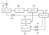
부가적인 실시예는 측정들이 웨이퍼들 상에서 수행되는 프로세스에 대해 동적 샘플링 방식을 형성하도록 구성된 시스템에 관한 것이다. 상기 시스템은 상기 웨이퍼들 상에서 측정들을 수행하도록 구성된 측정 툴을 포함한다. 상기 시스템은 또한 적어도 한 로트 내 모든 웨이퍼들에 대해 상기 웨이퍼들 상의 모든 측정 스팟들에서 측정들을 수행하도록 측정 툴을 제어하도록 구성된 하나 또는 둘 이상의 프로세서들을 포함한다. 상기 하나 또는 둘 이상의 프로세서들은 또한 최적 샘플링 방식, 증강된 샘플링 방식, 감소된 샘플링 방식, 및 상기 측정들의 결과들에 기초하여 상기 프로세스에 대한 동적 샘플링 방식에 대한 임계치들을 결정하도록 구성된다. 임계치들은 최적 샘플링 방식, 증강된 샘플링 방식, 및 감소된 샘플링 방식이 상기 프로세스를 위해 사용되어야 하는 측정들의 값들에 대응한다.An additional embodiment is directed to a system in which measurements are configured to form a dynamic sampling scheme for a process performed on wafers. The system includes a measurement tool configured to perform measurements on the wafers. The system also includes one or more processors configured to control a measurement tool to perform measurements at all measurement spots on the wafers for all wafers in at least one lot. The one or more processors are also configured to determine thresholds for a dynamic sampling scheme for the process based on an optimal sampling scheme, an augmented sampling scheme, a reduced sampling scheme, and results of the measurements. The thresholds correspond to the values of the measurements that the optimal sampling scheme, the enhanced sampling scheme, and the reduced sampling scheme should be used for the process.
일 실시예에서, 모든 측정 스팟들은 웨이퍼들 상의 모든 필드들, 웨이퍼들 상의 모든 타겟들, 또는 웨이퍼들 상의 모든 필드들 및 모든 타겟들을 포함한다. 또 다른 실시예에서, 상기 시스템은 미리결정된 간격들로 상기 동적 샘플링 방식을 형성하도록 구성된다. 부가적인 실시예에서, 측정들의 결과들은 측정들에서의 변동에 관한 정보를 포함한다. 추가 실시예에서, 상기 하나 또는 둘 이상의 프로세서들은 웨이퍼들 상에서 하나 또는 둘 이상의 다른 프로세스들을 수행했던 하나 또는 둘 이상의 툴들로부터의 정보와 결합하여 상기 측정들의 결과들에 기초하여 최적 샘플링 방식, 증강된 샘플링 방식, 및 감소된 샘플링 방식을 결정하도록 구성된다.In one embodiment, all measurement spots include all fields on wafers, all targets on wafers, or all fields on wafers and all targets. In another embodiment, the system is configured to form the dynamic sampling scheme at predetermined intervals. In an additional embodiment, the results of measurements include information about variations in measurements. In a further embodiment, the one or more processors, in combination with information from one or more tools that have performed one or more other processes on the wafers, determine an optimal sampling scheme, augmented sampling Method, and a reduced sampling scheme.
일 실시예에서, 최적 샘플링 방식, 증강된 샘플링 방식, 및 감소된 샘플링 방식은 상기 프로세스에서 측정될 다른 로트들에서의 다른 웨이퍼들의 갯수를 포함한다. 또 다른 실시예에서, 최적 샘플링 방식, 증강된 샘플링 방식, 및 감소된 샘플링 방식은 상기 프로세스에서 측정될 다른 로트들에서의 다른 웨이퍼들의 갯수 및 상기 프로세스 동안 상기 다른 웨이퍼들 각각에서 수행될 측정들의 하나 또는 둘 이상의 파라미터들을 포함한다.In one embodiment, the optimal sampling scheme, the augmented sampling scheme, and the reduced sampling scheme include the number of different wafers in different lots to be measured in the process. In yet another embodiment, the optimal sampling scheme, the augmented sampling scheme, and the reduced sampling scheme are based on the number of different wafers in different lots to be measured in the process and the number of measurements to be performed on each of the other wafers during the process Or two or more parameters.
일 실시예에서, 상기 하나 또는 둘 이상의 프로세서들은 다른 로트들에서의 다른 웨이퍼들 상에서 수행된 측정들의 값들과 임계치들을 비교함으로써, 그리고 샘플링 방식들 중 어떠한 것이, 측정들이 상기 비교 단계의 결과들에 기초하여 부가적인 로트들에서의 부가적인 웨이퍼들 상에서 수행되는 프로세스를 위해 사용될 것인지를 결정함으로써 동적 샘플링 방식을 수행한다. 그러한 실시예에서, 상기 하나 또는 둘 이상의 프로세서들은 측정 툴이 상기 부가적인 웨이퍼들 상에서 측정들을 수행하기 이전에, 상기 측정 툴의 하나 또는 둘 이상의 파라미터들을 변경시키도록 구성된다. 또 다른 실시예에서, 상기 측정 툴은 계측 툴로서 구성된다. 전술한 시스템의 각각의 실시예는 본 명세서에서 기술된 바와 같이 더 구성될 수 있다.In one embodiment, the one or more processors are configured to compare thresholds with values of measurements performed on different wafers in different lots, and to determine which of the sampling schemes are based on measurements based on the results of the comparison step Lt; / RTI > to be used for processes performed on additional wafers in additional lots. In such an embodiment, the one or more processors are configured to change one or more parameters of the measurement tool before the measurement tool performs measurements on the additional wafers. In yet another embodiment, the measurement tool is configured as a metrology tool. Each embodiment of the system described above may be further configured as described herein.
추가 실시예는 측정 프로세스 동안 웨이퍼들을 샘플링하기 위한 방법에 관한 것이다. 상기 방법은 측정 프로세스에 대한 복수 개의 샘플링 방식들을 설계하는 단계를 포함한다. 상기 방법은 또한 웨이퍼들에 대하여 복수 개의 샘플링 방식들 중 하나를 트리거링하는 단계를 포함한다. 부가하여, 상기 방법은 측정들이 트리거링된 샘플링 방식을 사용하여 측정 프로세스 동안 웨이퍼들 상에서 수행되도록 트리거링된 샘플링 방식을 활성화하는 단계를 포함한다. A further embodiment relates to a method for sampling wafers during a measurement process. The method includes designing a plurality of sampling schemes for the measurement process. The method also includes triggering one of a plurality of sampling schemes for the wafers. In addition, the method includes activating a sampling scheme triggered so that measurements are performed on the wafers during the measurement process using a triggered sampling scheme.
일 실시예에서, 복수 개의 샘플링 방식들을 설계하는 단계는 적어도 한 로트 내 모든 웨이퍼들에 대해 모든 웨이퍼들 상의 측정 스팟들에서 측정들을 수행하는 단계를 포함한다. 그러한 실시예에서, 상기 설계하는 단계는 모든 웨이퍼들 상에서 수행된 측정들에 기초하여, 최적 샘플링 방식, 증강된 샘플링 방식, 및 감소된 샘플링 방식을 결정하는 단계를 포함한다. 부가하여, 그러한 실시예는 측정들의 결과들에 기초하여, 최적 샘플링 방식, 증강된 샘플링 방식, 및 감소된 샘플링 방식을 트리거하기 위하여 사용될 임계치들을 결정하는 단계를 포함한다.In one embodiment, designing a plurality of sampling schemes includes performing measurements at measurement spots on all wafers for all wafers in at least one lot. In such an embodiment, the designing step includes determining an optimal sampling scheme, an augmented sampling scheme, and a reduced sampling scheme based on measurements performed on all wafers. In addition, such an embodiment includes determining thresholds to be used to trigger an optimal sampling scheme, an augmented sampling scheme, and a reduced sampling scheme, based on the results of the measurements.
일 실시예에서, 복수 개의 샘플링 방식들을 설계하는 단계는 적어도 한 로트 내 모든 웨이퍼들에 대해 모든 웨이퍼들 상의 모든 측정 스팟들에서 수행된 측정들의 결과들에 기초하여 복수 개의 샘플링 방식들을 설계하는 단계를 포함한다. 그러한 실시예에서, 트리거링된 샘플링 방식이 활성화된 웨이퍼들은 상기 적어도 한 로트와 다른 로트에 있다. 그러한 또 다른 실시예에서, 상기 측정들의 결과들은 로(raw) 측정 데이터를 포함하고, 상기 방법은 로우 측정 데이터에 기초하여 상기 복수 개의 샘플링 방식들을 설계하는 단계 이전에 절대값 또는 회귀 필터(regression filter)를 로우 측정 데이터에 적용하는 단계를 포함한다.In one embodiment, designing the plurality of sampling schemes includes designing a plurality of sampling schemes based on the results of measurements performed on all measurement spots on all wafers for all wafers in at least one lot . In such an embodiment, the activated wafers with the triggered sampling scheme are in a lot different from the at least one lot. In another such embodiment, the results of the measurements include raw measurement data, the method comprising the steps of determining an absolute value or a regression filter prior to designing the plurality of sampling schemes based on raw measurement data, ) To the row measurement data.
소정의 실시예들에서, 상기 복수 개의 샘플링 방식들을 설계하는 단계는 적어도 한 로트 내 모든 웨이퍼들에 대해 모든 웨이퍼들 상의 모든 측정 스팟들에서 수행되는 측정들의 결과들에 기초하여, 그리고 모든 웨이퍼들 상에서 하나 또는 둘 이상의 프로세스들을 수행했던 하나 또는 둘 이상의 툴들로부터의 정보에 기초하여 상기 복수 개의 샘플링 방식들을 설계하는 단계를 포함한다. 또 다른 실시예에서, 상기 복수 개의 샘플링 방식들을 설계하는 단계는 적어도 한 로트 내 모든 웨이퍼들에 대해 모든 웨이퍼들 상의 모든 측정 스팟들에서 수행되는 측정들의 결과들에 기초하여, 그리고 모든 웨이퍼들 상에서 수행된 하나 또는 둘 이상의 프로세스들에 대한 이력 프로세스 제어 데이터(historical process control data)에 기초하여 상기 복수 개의 샘플링 방식들을 설계하는 단계를 포함한다. 부가적인 실시예에서, 상기 복수 개의 샘플링 방식들을 설계하는 단계는 최적 기준 및 측정 프로세스 외부의 하나 또는 둘 이상의 제약들에 기초하여 복수 개의 샘플링 방식들을 설계하는 단계를 포함한다.In some embodiments, the step of designing the plurality of sampling schemes comprises: based on the results of measurements performed on all measurement spots on all wafers for all wafers in at least one lot, and on all wafers And designing the plurality of sampling schemes based on information from one or more tools that have performed one or more processes. In yet another embodiment, designing the plurality of sampling schemes may be based on results of measurements performed on all measurement spots on all wafers for all wafers in at least one lot, and on all wafers And designing the plurality of sampling schemes based on historical process control data for one or more processes. In an additional embodiment, designing the plurality of sampling schemes includes designing a plurality of sampling schemes based on one or more constraints outside the optimal reference and measurement process.
일 실시예에서, 복수 개의 샘플링 방식들을 설계하는 단계는 트리거링 단계에 대해 사용될 직접 임계치(direct threshold)들을 결정하는 단계를 포함한다. 또 다른 실시예에서, 트리거링 단계는 적어도 한 로트 내 모든 웨이퍼들에 대해 모든 웨이퍼들 상의 모든 측정 스팟들에서 수행된 측정들의 결과들을 직접 임계치들과 비교함으로써 개시된다. 부가적인 실시예에서, 트리거링 단계는 적어도 한 로트 내 모든 웨이퍼들에 대해 모든 웨이퍼들 상의 모든 측정 스팟들에서 수행된 측정들의 결과들의 통계적 속성들을 직접 임계치들과 비교함으로써 개시된다. 추가의 실시예에서, 트리거링 단계는 이력 프로세스 제어 데이터를 직접 임계치들과 비교함으로써 개시된다. 소정의 실시예들에서, 트리거링 단계는 하나 또는 둘 이상의 계측 툴들 또는 하나 또는 둘 이상의 프로세스 툴들로부터의 데이터를 직접 임계치들과 비교함으로써 개시된다.In one embodiment, designing a plurality of sampling schemes includes determining direct thresholds to be used for the triggering step. In yet another embodiment, the triggering step is initiated by comparing the results of measurements performed on all measurement spots on all wafers, with all of the wafers in at least one lot, directly to the thresholds. In an additional embodiment, the triggering step is initiated by comparing the statistical properties of the results of measurements performed on all measurement spots on all wafers to all thresholds directly for all wafers in a lot. In a further embodiment, the triggering step is initiated by comparing the history process control data directly to the thresholds. In certain embodiments, the triggering step is initiated by comparing data from one or more metrology tools or one or more process tools directly to the thresholds.
일 실시예에서, 복수 개의 샘플링 방식을 설계하는 단계는 트리거링 단계를 위해 사용될 비-직접 임계치(non-direct threshold)들을 결정하는 단계를 포함한다. 또 다른 실시예에서, 트리거링 단계는 시간 데이터를 비-직접 임계치들과 비교함으로써 개시된다. 부가적인 실시예에서, 트리거링 단계는 프로세스 툴 품질 제어 데이터를 비-직접 임계치들과 비교함으로써 개시된다. 추가의 실시예에서, 트리거링 단계는 생산 현장(production floor) 또는 재료 플래닝 데이터를 비-직접 임계치들과 비교함으로써 개시된다.In one embodiment, designing a plurality of sampling schemes includes determining non-direct thresholds to be used for the triggering step. In yet another embodiment, the triggering step is initiated by comparing the time data with non-direct thresholds. In an additional embodiment, the triggering step is initiated by comparing the process tool quality control data with non-direct thresholds. In a further embodiment, the triggering step is initiated by comparing production floor or material planning data with non-direct thresholds.
소정의 재료들 및 프로세스들이 웨이퍼에 매우 불균일한 응력을 야기할 수 있음이 발견되었다. 이러한 재료들 및 프로세스들에 대하여 전술한 전 범위 응력을 모니터링하기 위한 방법은 불균일한 응력을 정확히 결정하기에 적절하지 않다. 불균일한 응력의 정확한 규명의 결여는 하나의 패턴과 이전 패턴들과의 정렬이 불량한 웨이퍼의 소정 영역들에서 낮은 다이 수율들을 야기할 수 있다. 따라서, 웨이퍼들 상에서의 불균일한 응력을 규명하는 방법들 및 시스템들에 대한 필요성이 존재한다.It has been found that certain materials and processes can cause very non-uniform stress on the wafer. The method for monitoring the full-range stresses described above for these materials and processes is not suitable for accurately determining non-uniform stresses. The lack of precise identification of non-uniform stresses can result in low die yields in certain areas of the wafer where alignment of one pattern with previous patterns is poor. Thus, there is a need for methods and systems for identifying non-uniform stresses on wafers.
웨이퍼들 상에 설계 패턴을 프린트하기 위해 사용되는 패터닝 프로세스에 수정(correction)들을 가하고, 그에 의해 상기 프로세스들에 대한 수율을 증가시키기 위하여 웨이퍼들에 대하여 높은-차수 응력 또는 토포그래피(topography) 계측 결과들을 이용하는 실시예들이 제공된다. 본 명세서에서 기술되는 실시예들은 현재의 실시되는 것보다 더 세부적인(공간 해상도) 임계 프로세스 단계들에서 웨이퍼 응력 및/또는 토포그래피를 측정하기 위하여 사용될 수 있다. 상기 측정들은 웨이퍼들의 변형이 어떻게 패터닝 단계에 영향을 미칠 것인지를 결정하기 위해 모델에 입력될 수 있다. 상기 모델은 또한 상기 프로세스에 대한 높은-차수 수정들을 결정하고, 상기 높은-차수 수정들은 피드 포워드 루프(feed forward loop)로 노출 또는 패터닝 시스템에 제공될 수 있고, 그 결과 노출 또는 패터닝 시스템은 패터닝 단계 이전에 또는 패터닝 단계 동안 실시간 조정들을 할 수 있다. Order stress or topography measurement results for the wafers in order to apply corrections to the patterning process used to print the design pattern on the wafers, thereby increasing the yield for the processes Are provided. The embodiments described herein can be used to measure wafer stress and / or topography in more detailed (spatial resolution) critical process steps than currently practiced. The measurements may be entered into the model to determine how the deformation of the wafers will affect the patterning step. The model also determines the high-order modifications for the process, and the high-order modifications can be provided to the exposure or patterning system in a feed forward loop, such that the exposure or patterning system is subjected to a patterning step It is possible to make real-time adjustments before or during the patterning step.
여기서 기술된 실시예들은 앞서 기술한 방법들 및 시스템들과 상이한데, 그 이유는 노출 시스템들이 패터닝 단계의 준비로 웨이퍼들 상에서 계측을 수행하기 위해 이용가능한 시간 상의 비교적 심각한 제약들을 갖기 때문이다. 이러한 시간 제약들로 인하여, 인-시츄(in-situ) 계측 프로세스들은 현재, 후속의 패터닝 단계 동안 고차(high-order) 포커스 및 오버레이 수정들을 가능하게 하는 응력 및 변형 계측을 위한 비교적 높은 밀도의 샘플링을 포함하지 않는다. 본 명세서에서 기술된 실시예들은 다수의 이점들을 제공한다. 예를 들어, 리소그래피 노출 시스템들(예를 들어, 스캐너들)은 상당히 비쌀 수 있다. 193 nm 이머젼 스캐너(immersion scanner)는 약 3000만 달러에 이를 수 있다. 본 명세서에 기재된 실시예들은 노출 시스템들의 효율을 개선하기 위하여 사용될 수 있기 때문에, 본 명세서에서 기술되는 실시예들은 노출 시스템들의 사용자들에게 비교적 높은 가치가 있을 수 있다. The embodiments described herein are different from the methods and systems described above because the exposure systems have relatively severe constraints on the time available for performing the measurements on the wafers in preparation for the patterning step. Due to these time constraints, in-situ metrology processes are currently being used for relatively high density sampling for stress and strain metrology, which enables high-order focus and overlay corrections during subsequent patterning steps . The embodiments described herein provide a number of advantages. For example, lithographic exposure systems (e.g., scanners) can be quite expensive. The 193 nm immersion scanner can reach about 30 million dollars. As the embodiments described herein may be used to improve the efficiency of exposure systems, embodiments described herein may be of relatively high value to users of exposure systems.
일 실시예는 웨이퍼를 패터닝하기 위한 방법에 관한 것이다. 상기 방법은 웨이퍼 상에서 측정들을 수행하는 단계를 포함한다. 상기 방법은 또한 측정들의 결과들에 기초하여 웨이퍼의 변형을 모델링하는 단계를 포함한다. 부가하여, 상기 방법은 웨이퍼의 변형에 기초하여 패터닝 툴의 하나 또는 둘 이상의 파라미터들을 변경하는 단계를 포함한다. 상기 방법은 상기 변경 단계 이후에, 제 1 패턴 웨이퍼를 생성하기 위하여 패터닝 툴을 사용하여 웨이퍼를 패터닝하는 단계를 더 포함한다.One embodiment relates to a method for patterning a wafer. The method includes performing measurements on a wafer. The method also includes modeling the deformation of the wafer based on the results of the measurements. In addition, the method includes modifying one or more parameters of the patterning tool based on the deformation of the wafer. The method further includes, after the modifying step, patterning the wafer using a patterning tool to create a first patterned wafer.
일 실시예에서, 상기 측정들을 수행하는 단계는 웨이퍼에 대해 모든 측정 스팟들에서 측정들을 수행하는 단계를 포함한다. 또 다른 실시예에서, 측정들의 결과들은 응력 계측 데이터를 포함한다. 부가적인 실시예에서, 측정들의 결과들은 형태 계측 데이터를 포함한다. 추가 실시예에서, 측정들의 결과들은 오버레이 계측 데이터를 포함한다.In one embodiment, performing the measurements includes performing measurements at all measurement spots for the wafer. In another embodiment, the results of the measurements include stress metrology data. In an additional embodiment, the results of the measurements include morphometric data. In a further embodiment, the results of the measurements include overlay metrology data.
일 실시예에서, 웨이퍼의 변형을 모델링하는 단계는 웨이퍼가 패터닝 툴의 스테이지 상에 놓일 때 웨이퍼가 가질 변형을 추정하는 단계를 포함한다. 또 다른 실시예에서, 변형을 모델링하는 단계는 웨이퍼 상의 설계 패턴의 패터닝 상의 변형의 효과들을 시뮬레이팅하는 단계를 포함한다.In one embodiment, modeling the deformation of the wafer includes estimating the deformation that the wafer will have when the wafer is placed on the stage of the patterning tool. In yet another embodiment, modeling the deformation includes simulating effects of deformation on the patterning of the design pattern on the wafer.
일 실시예에서, 상기 방법은 제 1 패터닝된 웨이퍼 상에서 부가적인 측정들을 수행하는 단계, 상기 부가적인 측정들의 결과들에 기초하여 패터닝 툴의 하나 또는 둘 이상의 파라미터들을 변경하는 단계, 및 상기 부가적인 측정들의 결과들에 기초하여 패터닝 툴의 하나 또는 둘 이상의 파라미터들을 변경하는 단계 이후에, 제 2 패터닝된 웨이퍼를 생성하기 위하여 패터닝 툴을 사용하여 제 2 웨이퍼를 패터닝하는 단계를 포함한다. 그러한 실시예에서, 상기 부가적인 측정들의 결과들은 오버레이 계측 데이터를 포함한다. 그러한 또 다른 실시예에서, 상기 부가적인 측정들의 결과들은 포커스 계측 데이터를 포함한다. 그러한 부가적인 실시예에서, 상기 부가적인 측정들의 결과들은 도즈량(dose) 계측 데이터를 포함한다.In one embodiment, the method further comprises performing additional measurements on the first patterned wafer, modifying one or more parameters of the patterning tool based on the results of the additional measurements, And patterning the second wafer using a patterning tool to create a second patterned wafer, following the step of modifying one or more parameters of the patterning tool based on the results of the patterning tool. In such an embodiment, the results of the additional measurements include overlay metrology data. In another such embodiment, the results of the additional measurements include focus measurement data. In such additional embodiments, the results of the additional measurements include dose metering data.
일 실시예에서, 제 1 패터닝된 웨이퍼 및 제 2 패터닝된 웨이퍼는 동일한 로트에 있다. 또 다른 실시예에서, 제 1 패터닝된 웨이퍼 및 제 2 패터닝된 웨이퍼는 상이한 로트들에 있다.In one embodiment, the first patterned wafer and the second patterned wafer are in the same lot. In yet another embodiment, the first patterned wafer and the second patterned wafer are in different lots.
또 다른 실시예는 웨이퍼를 패터닝하도록 동작가능한 시스템에 관한 것이다. 상기 시스템은 웨이퍼 상에서 측정들을 수행하도록 동작가능한 측정 툴을 포함한다. 상기 시스템은 또한 측정들의 결과들에 기초하여 웨이퍼의 변형을 모델링하도록 동작가능한 하나 또는 둘 이상의 프로세서들을 포함한다. 상기 하나 또는 둘 이상의 프로세서들은 또한 웨이퍼의 변형에 기초하여 패터닝 프로세스의 하나 또는 둘 이상의 파라미터들을 변경시키도록 동작가능하다. 부가하여, 상기 시스템은 상기 패터닝 프로세스의 하나 또는 둘 이상의 파라미터들이 제 1 패터닝된 웨이퍼를 생성하기 위하여 변경된 이후에 패터닝 프로세스를 사용하여 웨이퍼를 패터닝하도록 동작가능한 패터닝 툴을 포함한다. 전술한 시스템의 실시예는 본 명세서에서 기술된 바와 같이 더 구성될 수 있다.Another embodiment is directed to a system operable to pattern a wafer. The system includes a measurement tool operable to perform measurements on a wafer. The system also includes one or more processors operable to model the deformation of the wafer based on the results of the measurements. The one or more processors are also operable to alter one or more parameters of the patterning process based on the deformation of the wafer. In addition, the system includes a patterning tool operable to pattern the wafer using a patterning process after one or more parameters of the patterning process have been modified to produce the first patterned wafer. Embodiments of the foregoing systems may be further configured as described herein.
전술한 방법 실시예들의 각각의 단계들 각각은 본 명세서에서 더 기술되는 바와 같이 수행될 수 있다. 부가하여, 전술한 방법들의 실시예들 각각은 본 명세서에서 기술된 임의의 다른 방법(들)의 임의의 다른 단계(들)를 포함할 수 있다. 부가하여, 전술한 방법들의 실시예들 각각은 본 명세서에서 기술된 시스템들 중 임의의 것에 의해 수행될 수 있다.Each of the steps of each of the above-described method embodiments may be performed as described further herein. In addition, each of the embodiments of the above-described methods may comprise any other step (s) of any other method (s) described herein. In addition, each of the embodiments of the above-described methods may be performed by any of the systems described herein.
본 발명의 추가 이점들은 첨부된 도면들을 참조하여 바람직한 실시예들에 대한 이하의 상세한 설명으로부터 당업자들에게 명백해질 수 있다.
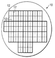
도 1은 웨이퍼 및 그 위에 형성된 필드들의 일 예시에 대한 상면도를 도시하는 개략적인 다이어그램이다.
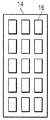
도 2는 웨이퍼 상의 하나의 필드 및 그 내부에 형성된 타겟들의 일 예시에 대한 상면도를 도시하는 개략적인 다이어그램이다.
도 3은 본 명세서에서 기술된 동적 샘플링 방식에 대한 일 실시예를 도시하는 개략적인 다이어그램이다.
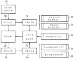
도 4는 측정들이 웨이퍼들 상에서 수행되는 프로세스에 대한 동적 샘플링 방식을 형성하도록 구성된 시스템에 대한 일 실시예를 도시하는 블록 다이어그램이다.
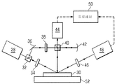
도 5는 웨이퍼들 상에서 측정들을 수행하도록 구성된 측정 툴의 일 실시예에 대한 측면도를 도시하는 개략적인 다이어그램이다.
도 6-도 7은 여러 방법 실시예들을 도시하는 흐름도이다.
도 8은 웨이퍼를 패터닝하도록 동작가능한 시스템에 대한 일 실시예를 도시하는 블록 다이어그램이다.
본 발명은 여러 다양한 변형예들 및 대안적인 형태들을 허용하지만, 본 발명의 특정 실시예들이 예의 방식으로 도면에 도시되고 본 명세서에서 상세히 기술될 수 있다. 도면들은 스케일링되지 않을 수 있다. 그러나 도면들 및 그에 대한 상세한 설명은 본 발명을 개시된 특정 형태로 제한하고자 하는 것이 아니라, 반대로 첨부된 청구범위에 의해 정의되는 바와 같이 본 발명의 사상 및 범위 내에 해당되는 모든 변형예들, 균등예들 및 대안예들을 커버하도록 의도됨이 이해되어야 한다.Additional advantages and features of the present invention will become apparent to those skilled in the art from the following detailed description of the preferred embodiments with reference to the accompanying drawings.
Figure 1 is a schematic diagram illustrating a top view of an example of a wafer and fields formed thereon.
Figure 2 is a schematic diagram showing a top view of one field on a wafer and an example of targets formed therein.
Figure 3 is a schematic diagram illustrating one embodiment of the dynamic sampling scheme described herein.
Figure 4 is a block diagram illustrating one embodiment of a system in which measurements are configured to form a dynamic sampling scheme for a process performed on wafers.
Figure 5 is a schematic diagram illustrating a side view of one embodiment of a measurement tool configured to perform measurements on wafers.
6-7 are flow charts illustrating various method embodiments.
8 is a block diagram illustrating an embodiment of a system operable to pattern a wafer.
While the invention is susceptible to various modifications and alternative forms, specific embodiments of the invention are shown by way of example in the drawings and may be described in detail herein. The drawings may not be scaled. It should be understood, however, that the drawings and detailed description thereto are not intended to limit the invention to the particular forms disclosed, but on the contrary, the intention is to cover all modifications, equivalents, and equivalents falling within the spirit and scope of the invention as defined by the appended claims ≪ / RTI > and alternatives.
본 명세서에서 사용되는 바와 같이, "웨이퍼"는 일반적으로 반도체 또는 비-반도체 재료로 형성된 기판을 지칭한다. 그러한 반도체 또는 비-반도체 재료의 예들은 단결정 실리콘, 갈륨 비소(gallium arsenide) 및 인듐 인화물(indium phosphide)을 포함하나, 이에 제한되지 않는다. 그러한 기판들은 반도체 제조 설비들에서 통상적으로 발견 및/또는 프로세싱될 수 있다. As used herein, "wafer" refers generally to a substrate formed of a semiconductor or non-semiconductor material. Examples of such semiconductor or non-semiconductor materials include, but are not limited to, monocrystalline silicon, gallium arsenide, and indium phosphide. Such substrates can typically be found and / or processed in semiconductor manufacturing facilities.
웨이퍼는 기판 상에 형성된 하나 또는 둘 이상의 층들을 포함할 수 있다. 예를 들어, 그러한 층들은 레지스트, 절연 재료, 도전성 재료 및 반도체 재료를 포함하나, 이에 제한되는 것은 아니다. 다수의 상이한 타입들의 그러한 층들이 당업계에 공지되어 있고, 본 명세서에서 사용되는 용어 "웨이퍼"는 모든 타입들의 그러한 층들을 포함하는 웨이퍼를 망라하는 것으로 의도된다. The wafer may comprise one or more layers formed on a substrate. For example, such layers include, but are not limited to, resist, insulating material, conductive material, and semiconductor material. Many different types of such layers are known in the art, and the term "wafer" as used herein is intended to encompass a wafer comprising all such layers of such type.
웨이퍼 상에 형성된 하나 또는 둘 이상의 층들은 패터닝될 수 있다. 예를 들어, 웨이퍼는 복수 개의 다이들을 포함할 수 있고, 각각의 다이는 반복가능한 패터닝된 피쳐(feature)들을 갖는다. 그러한 재료의 층들의 형성 및 프로세싱은 궁극적으로 완성된 장치들을 야기할 수 있다. 다수의 상이한 타입들의 장치들은 웨이퍼 상에서 형성될 수 있고, 본 명세서에서 사용되는 용어 "웨이퍼"는 당업계에 공지된 임의 타입의 장치가 제조되어 있는 웨이퍼를 포함하는 것으로 의도된다.One or more layers formed on the wafer may be patterned. For example, the wafer may include a plurality of dies, each having repeatable patterned features. The formation and processing of such layers of material may ultimately lead to finished devices. A number of different types of devices may be formed on a wafer, and the term "wafer" as used herein is intended to encompass a wafer on which any type of device known in the art is manufactured.
이제 도면들을 살펴보면, 도면들은 스케일링되어 도시되지 않았다. 특히, 도면들의 소정 엘리먼트들의 스케일은 그러한 엘리먼트들의 특성들을 강조하기 위하여 많이 과장된다. 또한 도면들은 동일한 스케일로 도시되지 않는다. 유사하게 구성될 수 있는, 하나보다 많은 도면들에 도시된 엘리먼트들은 동일한 참조 개수들을 사용하여 표시되었다.Turning now to the drawings, the figures are not drawn to scale. In particular, the scale of certain elements of the figures is greatly exaggerated to emphasize the characteristics of those elements. Also, the figures are not drawn to scale. Elements shown in more than one of the figures, which may be similarly constructed, have been denoted using the same reference numbers.
*일 실시예는 웨이퍼들 상에서 측정들이 수행되는 프로세스에 대한 동적 샘플링 방식을 형성하기 위한 방법에 관한 것이다. 일 실시예에서, 상기 프로세스는 계측 프로세스를 포함한다. 이러한 방식으로, 상기 방법은 계측 프로세스에 대한 동적 샘플링 방식을 형성하는 단계를 포함할 수 있다. 계측 프로세스는 본 명세서에서 더 기술된 임의의 측정들을 포함할 수 있다. 계측 프로세스는 또한 하나 또는 둘 이상의 상이한 측정들을 포함할 수 있다. 부가하여, 계측 프로세스는 당업계에 공지된 임의의 다른 적합한 계측 프로세스를 포함할 수 있다. 부가하여, 계측 프로세스는 계측 프로세스 이전에 웨이퍼들 상에서 수행되는 제조 프로세스에 따라 변화할 수 있다. 예를 들어, 상이한 계측 프로세스들은 상이한 제조 프로세스들을 모니터링 및 제어하기에 적합한 상이한 특성들을 측정하기에 적절할 수 있다. 이러한 방식으로, 동적 샘플링 방식을 형성하는 방법을 수행하기에 앞서, 웨이퍼들은 제조 프로세스를 사용하여 프로세싱될 수 있다. 웨이퍼들 상에서 수행되는 제조 프로세스는 당업계에 공지된 임의의 제조 프로세스를 포함할 수 있다. 그와 같이, 본 명세서에 기술된 상기 방법들은 임의의 제조 프로세스를 모니터링하고 제어하기 위해 사용된 임의의 계측 프로세스에 대한 동적 샘플링 방식을 형성하기 위해 사용될 수 있다.One embodiment relates to a method for forming a dynamic sampling scheme for a process in which measurements are performed on wafers. In one embodiment, the process comprises a metrology process. In this manner, the method may include forming a dynamic sampling scheme for the metrology process. The metrology process may include any of the measurements described further herein. The metrology process may also include one or more different measurements. In addition, the metrology process may include any other suitable metrology process known in the art. In addition, the metrology process may vary depending on the manufacturing process performed on the wafers prior to the metrology process. For example, different metering processes may be appropriate to measure different characteristics suitable for monitoring and controlling different manufacturing processes. In this manner, prior to performing the method of forming the dynamic sampling scheme, the wafers can be processed using the fabrication process. The manufacturing process performed on the wafers may include any manufacturing process known in the art. As such, the methods described herein can be used to form a dynamic sampling scheme for any metrology process used to monitor and control any manufacturing process.
계측 프로세스를 위한 동적 샘플링 방식은 이하의 파라미터들 각각 또는 이들의 소정 조합을 포함할 수 있다: 샘플링 로트들에서의 빈도(frequency); 웨이퍼들의 개수; 웨이퍼들의 개수 지정(numeric designation); 필드들의 개수; 웨이퍼 상의 필드들의 위치들; 각 필드 내 사이트들의 개수; 필드 내 사이트들의 위치들; 계측 타겟의 타입; 또는 측정 알고리즘들. 동적 샘플링 방식에 따라 웨이퍼들을 샘플링하는 방법은 복수 개의 샘플링 방식들을 설계하는 단계, 샘플링 방식을 트리거링하는 단계, 및 트리거링된 샘플링 방식을 활성화하는 단계를 포함할 수 있다. 이러한 단계들 각각은 본 명세서에서 더 기술된 바와 같이 수행될 수 있다.The dynamic sampling scheme for the metrology process may include each of the following parameters or some combination thereof: frequency in sampling lots; The number of wafers; Numeric designation of wafers; Number of fields; The locations of the fields on the wafer; The number of sites in each field; The locations of sites within the field; The type of measurement target; Or measurement algorithms. A method of sampling wafers according to a dynamic sampling scheme may include designing a plurality of sampling schemes, triggering a sampling scheme, and activating a triggered sampling scheme. Each of these steps may be performed as described further herein.
본 방법은 웨이퍼들에 대해 모든 측정 스팟들에서 적어도 한 로트 내 모든 웨이퍼들 상에서 측정들을 수행하는 단계를 포함한다. 이러한 단계는 본 명세서에서 "전지적 샘플링(omniscient sampling)"으로서 지칭된다. 웨이퍼들의 한 "로트(lot)"는 본 명세서에서 일반적으로 제조 프로세스들에서 하나의 그룹으로서 집합적으로 또는 차례로 프로세싱되는 복수 개의 웨이퍼들로서 정의된다. 일 실시예에서, 모든 측정 스팟들은 웨이퍼들 상의 모든 필드들을 포함한다. 예를 들어, 도 1에 도시된 바와 같이, 웨이퍼(10)는 그 위에 형성된 필드들(12)을 갖는다. 비록 웨이퍼(10) 상의 특정 개수 및 배열의 필드들(12)이 도 1에 도시되어 있지만, 웨이퍼 상의 필드들의 개수 및 배열은 예를 들어, 웨이퍼들 상에 형성되어 있는 장치에 따라 가변될 수 있다. 측정들은 웨이퍼(10) 상에 형성된 모든 필드들(12) 및 적어도 한 로트 내 다른 웨이퍼들 상의 모든 필드들에서 수행될 수 있다. 예를 들어, 측정들은 적어도 하나의 로트 내 모든 웨이퍼들 상에서 형성된 필드 당 적어도 한 번 수행될 수 있다. 측정들은 필드들에 형성된 장치 구조들 상에서, 그리고/또는 필드들에 형성된 테스트 구조들 상에서 수행될 수 있다. 부가하여, 각각의 필드에서 수행된 측정들은 계측 프로세스 동안 수행된 모든 측정들(예를 들어, 하나 또는 둘 이상의 상이한 측정들)을 포함할 수 있다. The method includes performing measurements on all wafers in at least one lot in all measurement spots for wafers. This step is referred to herein as "omniscient sampling ". A "lot " of wafers is generally defined herein as a plurality of wafers that are collectively or sequentially processed as a group in manufacturing processes. In one embodiment, all measurement spots include all the fields on the wafers. For example, as shown in FIG. 1, the
또 다른 실시예에서, 모든 측정 스팟들은 적어도 하나의 로트 내 웨이퍼들 상의 모든 타겟들을 포함한다. 예를 들어, 도 2에 도시된 바와 같이, 웨이퍼(도 2에는 미도시) 상에 형성된 필드(14)는 타겟들(16)을 포함할 수 있다. 비록 필드(14)내의 특정 개수 및 배열의 타겟들(16)이 도 2에 도시되었지만, 필드들 내의 타겟들의 개수 및 배열은 예를 들어, 웨이퍼 상에 형성된 장치에 따라 가변될 수 있다. 타겟들(16)은 장치 구조들 및/또는 테스트 구조들을 포함할 수 있다. 따라서, 이러한 실시예에서, 측정들이 필드(14)에 형성된 모든 타겟들(16) 상에서 수행될 수 있다. 부가하여, 측정들은 필드(14) 내 형성된 타겟 당 적어도 한 번 수행될 수 있다. 측정들은 또한 계측 프로세스 동안 수행된 모든 측정들(예를 들어, 하나 또는 둘 이상의 상이한 측정들)을 포함할 수 있다.In another embodiment, all measurement spots include all targets on at least one in-lot wafers. For example, as shown in FIG. 2, a
부가적인 실시예에서, 모든 측정 스팟들은 적어도 하나의 로트 내 웨이퍼들 상의 모든 필드들 및 모든 타겟들을 포함한다. 예를 들어, 도 1에서 웨이퍼(10) 상에 형성된 것으로 도시된 각각의 필드들(12)은 도 2에 도시된 타겟들(16)과 같은 하나 또는 둘 이상의 타겟들을 포함할 수 있다. 따라서, 측정들은 적어도 하나의 로트 내 웨이퍼들의 각각에 형성된 필드들 각각의 타겟들 각각 상에서 수행될 수 있다.In an additional embodiment, all measurement spots include all fields and all targets on at least one in-lot wafers. For example, each of the
일 실시예에서, 전지적 샘플링 단계에서 수행된 측정들의 결과들은 측정들의 변동에 관한 정보를 포함한다. 측정들의 변동은 당업계에 공지된 임의의 방식(예를 들어, 표준 편차, 변동의 양 등)으로 결정될 수 있다. 측정들의 변동이 일반적으로 프로세스에서의 변동들 또는 프로세스 이탈(process excursion)들을 지시할 것이기 때문에, 전지적 샘플링 단계에서 측정된 웨이퍼들의 로트들의 개수는 프로세스 또는 프로세스 이탈들에 따라 가변될 수 있다. 그와 같이, 비록 적어도 하나의 로트가 전지적 샘플링 단계에서 측정되지만, 측정되는 로트들의 개수는 각각의 샘플링된 로트에 대한 측정들의 결과들에 따라 3 로트, 4 로트, 5 로트 등이 될 수 있다. 이러한 방식으로, 상기 방법은 모든 웨이퍼들 및 웨이퍼들 상의 모든 필드들 및/또는 모든 타겟들이 측정되는 다수의 로트들의 전지적 샘플링으로 시작되고, 변동의 원인들이 발견된다. 이러한 단계에서 식별되거나 결정된 변동의 원인들은 오버레이 변동, 임계 치수(critical dimension; CD) 변동, 웨이퍼들의 다른 특성들의 변동, 로트-대-로트(lot-to-lot) 변동, 웨이퍼-대-웨이퍼 변동, 필드-대-필드 변동, 측면-대-측변(side-to-side) 변동, 변동의 통계적 원인들 및 이와 유사한 것 또는 이들의 임의 조합을 포함하는 임의의 변동 원인들을 포함할 수 있고, 앞서 열거된 변동 원인들에 제한되지 않는다.In one embodiment, the results of the measurements performed in the battery sampling step include information about variations in measurements. Variations in measurements can be determined in any manner known in the art (e.g., standard deviation, amount of variation, etc.). The number of lots of wafers measured in the global sampling step may vary depending on the process or process departures, since variations in the measurements will generally indicate variations in the process or process excursions. As such, although the at least one lot is measured at the battery sampling stage, the number of lots to be measured may be 3 lots, 4 lots, 5 lots, etc. depending on the results of the measurements for each sampled lot. In this manner, the method begins with an electronic sampling of a number of lots in which all the fields and / or all the targets on all the wafers and wafers are measured, and the causes of variations are found. The causes of the variation identified or determined at this stage include variations in overlay variation, critical dimension (CD), variation in other characteristics of the wafers, lot-to-lot variation, wafer-to- May include any variation causes, including field-to-field variations, side-to-side variations, statistical causes of variations, and the like, or any combination thereof, It is not limited to the listed variation causes.
상기 방법은 또한 측정들의 결과들에 기초하여 최적 샘플링 방식, 증강된 샘플링 방식, 감소된 샘플링 방식, 및 프로세스에 대한 동적 샘플링 방식에 대한 임계치들을 결정하는 단계를 포함한다. 일반적으로, 증강된 샘플링 방식은 최적 샘플링 방식보다 더 높은 샘플링을 위한 것이고, 감소된 샘플링 방식은 최적 샘플링 방식보다 더 낮은 샘플링을 위한 것이다. 즉, 증강된 샘플링 방식은 최적 샘플링 방식보다 더 높은 샘플링 레이트를 갖는 반면, 감소된 샘플링 방식은 최적 샘플링 방식보다 더 낮은 샘플링 레이트를 갖는다. 이러한 방식으로, 최적 샘플링 방식이 결정될 수 있고, 그 다음 증강된 샘플링 방식 및 감소된 샘플링 방식이 최적 샘플링 방식으로부터 결정될 수 있다. 예를 들어, 측정들의 결과들이 제조 프로세스가 CD의 현저한 측면-대-측면 변동을 나타내나 CD의 현저한 웨이퍼-대-웨이퍼 변동을 나타내지 않음을 지시한다면, 최적 샘플링 방식은 하나의 로트 내 단지 소수 개의 웨이퍼들의 양쪽 측면들 상에 현저한 개수의 CD의 측정들을 포함할 수 있다. 반대로, 측정들의 결과들이 제조 프로세스가 오버레이에서 현저한 웨이퍼-대-웨이퍼 변동을 나타내나 오버레이에서 현저한 측면-대-측면 변동을 나타내지 않음을 지시한다면, 최적 샘플링 방식은 현저한 개수의 웨이퍼들의 측정들을 포함할 수 있으나, 각각의 웨이퍼에 걸쳐서는 단지 소수 번의 측정들을 포함할 수 있다. 전술한 위 예들 양쪽 모두에서, 증강된 샘플링 방식 및 감소된 샘플링 방식은 최적 샘플링 방식에 기초하여 결정될 수 있다.The method also includes determining thresholds for an optimal sampling scheme, an augmented sampling scheme, a reduced sampling scheme, and a dynamic sampling scheme for the process based on the results of the measurements. In general, the augmented sampling scheme is for higher sampling than the optimal sampling scheme, and the reduced sampling scheme is for lower sampling than the optimal sampling scheme. That is, the augmented sampling scheme has a higher sampling rate than the optimal sampling scheme, while the reduced sampling scheme has a lower sampling rate than the optimal sampling scheme. In this way, an optimal sampling scheme can be determined, and then an augmented sampling scheme and a reduced sampling scheme can be determined from the optimal sampling scheme. For example, if the results of the measurements indicate that the fabrication process exhibits significant side-to-side variations of the CD or does not exhibit significant wafer-to-wafer variation of the CD, then the optimal sampling scheme may include only a few And may include measurements of a significant number of CDs on both sides of the wafers. Conversely, if the results of the measurements indicate that the fabrication process exhibits significant wafer-to-wafer variation in the overlay or does not exhibit significant side-to-side variation in the overlay, then the optimal sampling scheme includes measurements of a significant number of wafers But may include only a small number of measurements across each wafer. In both of the above examples, the augmented sampling scheme and the reduced sampling scheme can be determined based on the optimal sampling scheme.
임계치들은 계측 프로세스를 위하여 최적 샘플링 방식, 증강된 샘플링 방식 및 감소된 샘플링 방식이 사용되어야 하는 측정들의 값들에 대응한다. 예를 들어, 도 3에 도시된 바와 같이, 임계치들은 임계치 1 및 임계치 2를 포함할 수 있다. 임계치 1은 그 아래에서 계측 프로세스를 위해 감소된 샘플링 방식이 사용되어야 하는 측정들의 값들에 대응한다. 임계치 2는 그 위에서 계측 프로세스를 위해 증강된 샘플링 방식이 사용되어야 하는 측정들의 값들에 대응한다. 도 3에 도시된 바와 같이, 임계치 1과 임계치 2 사이의 측정들의 값들은 계측 프로세스를 위해 최적 샘플링 방식이 사용되어야 하는 측정들의 값들에 대응한다.The thresholds correspond to the values of the measurements for which an optimal sampling scheme, an augmented sampling scheme and a reduced sampling scheme are to be used for the metering process. For example, as shown in FIG. 3, the thresholds may include threshold 1 and threshold 2. Threshold 1 corresponds to the values of the measurements below which the reduced sampling scheme should be used for the metering process. Threshold 2 corresponds to the values of the measurements above which the augmented sampling scheme should be used for the metering process. As shown in FIG. 3, the values of the measurements between the threshold 1 and the threshold 2 correspond to the values of the measurements for which the optimal sampling scheme should be used.
임계치들이 그에 대응하고 임계치들과 비교되는 측정들의 값들은 측정들의 변동을 포함할 수 있다. 측정들의 변동은 당업계에 공지된 임의의 방식(예를 들어, 표준 편차, 변동의 양, 등)으로 결정될 수 있다. 예를 들어, 임계치들의 값들은 CD, 오버레이 또는 웨이퍼들의 임의의 다른 측정가능한 특성에서의 변동들의 상이한 값들에 대응할 수 있고, 임계치들 위의 하나의 값에서 증강된 샘플링 방식이 최적 샘플링 방식 대신에 사용되고, 임계치들 아래의 또 다른 값에서 감소된 샘플링 방식이 최적 샘플링 방식 대신에 사용된다. 그러한 예에서, 하나의 임계치는 미리결정된 변동의 퍼센티지에 대응할 수 있고, 상기 미리결정된 변동의 퍼센티지 위에서 증강된 샘플링이 사용되어야 한다. 이러한 방식으로, 최적 샘플링 방식을 사용하여 한 로트의 웨이퍼들 상에서 수행된 측정들이 그러한 로트에 걸쳐 미리결정된 변동의 퍼센티지(예를 들어, 10% 변동, 20% 변동 등)보다 더 높은 변동의 퍼센티지를 나타낸다면, 증강된 샘플링 방식이 부가적인 로트들의 웨이퍼들 상에서 수행된 측정 프로세스에 대하여 선택될 수 있다. 그러나, 임계치들이 대응하는, 그리고 임계치들과 비교될 수 있는 측정들의 값들은 측정들의 값들 그 자체를 포함할 수 있다. 예를 들어, 임계치들의 값들은 웨이퍼들의 CD, 오버레이 또는 임의의 다른 측정가능한 특성의 상이한 값들에 대응할 수 있고, 하나의 값은 그 값을 초과하여 최적 샘플링 방식 대신에 증강된 샘플링 방식이 사용되고 또 다른 값은 그 값 미만에서 최적 샘플링 방식 대신에 감소된 샘플링 방식이 사용된다.The values of the measurements for which the thresholds correspond and for which the thresholds are compared may include variations in the measurements. The variation in measurements may be determined in any manner known in the art (e.g., standard deviation, amount of variation, etc.). For example, the values of the thresholds may correspond to different values of variations in the CD, overlay or any other measurable characteristic of the wafers, and an enhancement sampling scheme at one value above the thresholds may be used instead of the optimal sampling scheme , A reduced sampling scheme at another value below the thresholds is used instead of the optimal sampling scheme. In such an example, one threshold may correspond to a percentage of a predetermined variation, and augmented sampling should be used on a percentage of the predetermined variation. In this way, measurements performed on a lot of wafers using an optimal sampling scheme can be used to determine a percentage of variation that is higher than a percentage of a predetermined variation (e.g., 10% variation, 20% variation, etc.) An enhanced sampling scheme may be selected for the measurement process performed on the wafers of additional lots. However, the values of the measurements to which the thresholds correspond and to which the thresholds can be compared may include the values of the measurements themselves. For example, the values of the thresholds may correspond to different values of the CD, overlay or any other measurable characteristic of the wafers, and one value may exceed that value so that an augmented sampling scheme is used instead of an optimal sampling scheme, A value less than that value uses a reduced sampling scheme instead of an optimal sampling scheme.
측정들의 변동의 값들은 일반적으로 프로세스의 변동들 또는 프로세스 이탈들을 나타내기 때문에, 동적 샘플링 방식은 제조 프로세스가 어떻게 "거동하고 있는지"에 기초하여 샘플링 방식을 조정할 수 있다. 특히, 높은 변동들을 갖는 프로세스들에 대하여, 높은 샘플링 레이트 또는 증강된 샘플링 방식이 선택된다. 이러한 방식으로, 높은 변동들을 갖는 프로세스들에 대하여, 로트 당 더 많은 웨이퍼들, 웨이퍼 당 더 많은 측정들 등이 증강된 샘플링 방식을 선택함으로써 수행될 수 있다. 반대로, 낮은 변동들을 갖는 프로세스들에 대하여, 낮은 샘플링 레이트 또는 감소된 샘플링 방식이 선택된다. 그와 같이, 낮은 변동들을 가진 프로세스들에 대하여, 로트 당 더 적은 개수의 웨이퍼들, 웨이퍼 당 더 적은 개수의 측정들 등이 감소된 샘플링 방식을 선택함으로써 수행될 수 있다. 이러한 방식으로, 본 명세서에서 기술된 실시예들은 유리한데, 그 이유는 상기 실시예들이 불량한 성능(예를 들어, 높은 변동들)을 나타내고 있는 프로세스들에 대한 증가된 정보를 제공하기 위해 사용될 수 있고, 이것은 더 정확한 프로세스 제어 및 모니터링을 위해 사용되어, 수율을 증가시킬 수 있으며, 상기 실시예들은 우수한 성능(예를 들어, 낮은 변동들)을 나타내고 있는 프로세스들에 대한 더 정보를 제공하기 위해 사용될 수 있고, 이것은 이러한 프로세스들에 대해 수행되는 측정들의 횟수를 감소시킴으로써 처리량을 증가시킬 수 있기 때문이다.Because the values of the variations in measurements generally indicate process variations or process deviations, the dynamic sampling scheme can adjust the sampling scheme based on how the manufacturing process is "behaving". In particular, for processes with high variations, a high sampling rate or an augmented sampling scheme is selected. In this way, for processes with high variations, more wafers per lot, more measurements per wafer, etc. can be performed by selecting an enhanced sampling scheme. Conversely, for processes with low variations, a low sampling rate or a reduced sampling scheme is selected. As such, for processes with low variations, fewer wafers per lot, fewer measurements per wafer, etc. can be performed by selecting a reduced sampling scheme. In this way, the embodiments described herein are advantageous because the embodiments can be used to provide increased information for processes exhibiting poor performance (e. G., High fluctuations) , Which may be used for more accurate process control and monitoring, may increase yield, and the embodiments may be used to provide more information about processes exhibiting superior performance (e. G., Lower fluctuations) , Which can increase throughput by reducing the number of measurements performed on these processes.
따라서 본 명세서에 기술된 실시예들은 본 명세서에서 기술된 대로 형성된 동적 샘플링 방식들이 제조 프로세스 변동들 또는 이탈들에 더 민감하다는 점에서 다른 샘플링을 위한 방법들 및 시스템들에 비해 유리하다. 특히, 프로세스 이탈들이 발생하면, 샘플링 방식(또는 샘플링 레이트)이 조정된다. 부가하여, 전술한 바와 같이, 동적 샘플링 방식은 전지적 샘플링 단계에서 수행된 측정들의 결과들에 기초하여 형성된다. 따라서, 본 명세서에서 기술된 전지적 샘플링은 이전에 사용된 모델들보다 동적 샘플링 방식을 형성하기 위하여 더 많은 결정 기준들을 제공하기 때문에, 본 명세서에서 기술된 실시예들은 또한 모델을 이용하는 현재 사용되는 동적 샘플링을 위한 방법들 및 시스템들보다 더 유리하다.Thus, the embodiments described herein are advantageous over methods and systems for other sampling in that the dynamic sampling schemes formed as described herein are more sensitive to manufacturing process variations or deviations. In particular, when process deviations occur, the sampling scheme (or sampling rate) is adjusted. In addition, as described above, the dynamic sampling scheme is formed based on the results of measurements performed in the battery sampling step. Thus, because the battery sampling described herein provides more determination criteria to form a dynamic sampling scheme than the previously used models, the embodiments described herein may also be used in conjunction with currently used dynamic sampling Are more advantageous than methods and systems for < RTI ID = 0.0 >
전술한 바와 같이, 상이한 샘플링 방식들 및 임계치들이 전지적 샘플링의 결과들로부터 결정될 수 있다. 그러나, 프로세싱(즉, 제조) 툴들로부터의 정보가 전지적 샘플링의 결과들에 부가될 수 있고, 임계치들에 부가하여 최적 샘플링 방식, 증강된 샘플링 방식 및 감소된 샘플링 방식을 선택하기 위하여 사용될 수 있다. 예를 들어, 일 실시예에서, 최적 샘플링 방식, 증강된 샘플링 방식 및 감소된 샘플링 방식은 웨이퍼들 상에서 하나 또는 둘 이상의 다른 프로세스들을 수행했던 하나 또는 둘 이상의 툴들로부터의 정보와 결합하여 측정들의 결과들에 기초하여 결정될 수 있다. 상기 하나 또는 둘 이상의 툴들은 당업계에 공지된 임의의 제조 툴들(예를 들어, 리소그래피 툴들, 에칭 툴들, 증착 툴들, 이온 주입 툴들, 화학적-기계적 연마(CMP) 툴들 등)을 포함할 수 있다. 상기 하나 또는 둘 이상의 툴들로부터 나온 정보는 제조 툴(들)의 소정의 품질 계측치 또는 제조 툴(들)로부터 획득될 수 있거나 제조 툴(들)에 의해 생성되는 임의의 다른 정보를 포함할 수 있다. 따라서, 상기 하나 또는 둘 이상의 툴들로부터 나온 정보는 전지적 샘플링 단계 동안 측정된 웨이퍼들의 제조 프로세스 이력을 포함할 수 있다. 상기 하나 또는 둘 이상의 툴들로부터 나온 정보는 당업계에서 임의의 공지된 방식으로 획득될 수 있다. 예를 들어, 상기 정보는 상기 하나 또는 둘 이상의 툴들에 결합된 저장 매체 또는 프로세스로부터 직접 획득될 수 있다. 대안적으로, 상기 정보는 상기 하나 또는 둘 이상의 툴들로부터 간접적으로 획득될 수 있다. 예를 들어, 상기 하나 또는 둘 이상의 툴들은 팹 데이터베이스와 같은 데이터베이스로 정보를 전송할 수 있고, 상기 정보는 그러한 데이터베이스 또는 임의의 다른 적합한 저장 매체로부터 획득될 수 있다. 상기 하나 또는 둘 이상의 툴들로부터 나온 정보는 당업계에 공지된 임의의 적합한 포맷을 가질 수 있다.As described above, different sampling schemes and thresholds can be determined from the results of the global sampling. However, information from processing (i. E., Manufacturing) tools may be added to the results of the battery sampling and used in addition to the thresholds to select an optimal sampling scheme, an augmented sampling scheme, and a reduced sampling scheme. For example, in one embodiment, the optimal sampling scheme, the augmented sampling scheme, and the reduced sampling scheme combine with the information from one or more tools that have performed one or more different processes on the wafers, . ≪ / RTI > The one or more tools may include any of the manufacturing tools known in the art (e.g., lithography tools, etching tools, deposition tools, ion implantation tools, chemical-mechanical polishing (CMP) tools, etc.). The information from the one or more tools may be obtained from a predetermined quality metric or manufacturing tool (s) of the manufacturing tool (s) or may include any other information generated by the manufacturing tool (s). Thus, the information from the one or more tools may include the manufacturing process history of the wafers measured during the global sampling step. The information from the one or more tools may be obtained in any known manner in the art. For example, the information may be obtained directly from a storage medium or process coupled to the one or more tools. Alternatively, the information may be obtained indirectly from the one or more tools. For example, the one or more tools may transfer information to a database, such as a fab database, and the information may be obtained from such database or any other suitable storage medium. The information from the one or more tools may have any suitable format known in the art.
동적 샘플링 방식을 형성하기 위하여 전지적 샘플링에 의해 수행된 측정들의 결과들과 결합하여 웨이퍼들 상에서 하나 또는 둘 이상의 제조 프로세스들을 수행했던 하나 또는 둘 이상의 툴들로부터의 정보를 사용하는 것은 다수의 이유들로 유리할 수 있다. 예를 들어, 상기 하나 또는 둘 이상의 툴들로부터 나온 정보는 웨이퍼들을 제조하기 위해 사용된 프로세스(들)가 상기 프로세스(들)에 대한 프로세스 윈도우(들) 내에서 동작하고 있는지 여부 및/또는 프로세스 윈도우(들) 내의 어디에서 상기 프로세스(들)가 동작하고 있는지를 결정하기 위해 사용될 수 있다. 이러한 방식으로, 상기 하나 또는 둘 이상의 툴들로부터 나온 정보는 전지적 샘플링에 의해 수행된 측정들의 결과들이 공칭 프로세스 변동들을 나타내고 있는 프로세스에 대해 예상될 수 있는 결과들을 나타내는지, 공칭 프로세스 변동들보다 더 낮은 변동들을 나타내고 있는 프로세스에 대해 예상될 수 있는 결과들을 나타내는지, 또는 공칭 프로세스 변동들보다 더 높은 변동들을 나타내고 있는 프로세스에 대해 예상될 수 있는 결과들을 나타내는지를 결정하기 위해 사용될 수 있다. 따라서, 상기 정보는 전지적 샘플링에 의해 수행된 측정들의 결과들이 최적 샘플링 방식(공칭 또는 "표준" 프로세스 변동들), 감소된 샘플링 방식(공칭 프로세스 변동들보다 더 낮음), 또는 증강된 샘플링 방식(공칭 프로세스변동들보다 더 높음)에 대응하는지를 결정하고, 임계치들을 적절히 설정하기 위해 사용될 수 있다.Using information from one or more tools that have performed one or more fabrication processes on wafers in combination with the results of measurements performed by cell sampling to form a dynamic sampling scheme is advantageous for a number of reasons . For example, information from the one or more tools may indicate whether the process (s) used to manufacture the wafers are operating within the process window (s) for the process (s) and / (S) in which the process (s) are operating. In this manner, the information from the one or more tools may indicate whether the results of the measurements performed by the battery sampling represent the expected results for the process exhibiting nominal process variations, a lower change than the nominal process variations Or indicate results that can be expected for a process exhibiting higher fluctuations than nominal process variations. ≪ RTI ID = 0.0 > [0035] < / RTI > Thus, the information can be used to determine whether the results of measurements performed by the battery sampling are optimal sampling schemes (nominal or "standard" process variations), reduced sampling schemes (lower than nominal process variations) Higher than process variations), and may be used to set the thresholds appropriately.
전지적 샘플링 동안 측정된 웨이퍼들은 또한 제조 툴(들)의 의도적으로 상이한 파라미터들에서 제조 툴(들)에 의해 프로세싱된 웨이퍼들을 포함할 수 있다. 따라서, 전지적 샘플링 동안 수행된 측정들의 결과들의 변동들 및 웨이퍼들이 프로세싱된 제조 툴(들)의 파라미터들은 임계치들을 결정하기 위해 사용될 수 있다. 예를 들어, 증강된 샘플링 방식과 최적 샘플링 방식 사이의 임계치는 프로세스 윈도우의 에지들에서 또는 그 근처에서 프로세싱된 웨이퍼들 상에서 수행된 측정들의 결과들에 기초하여 결정될 수 있다. 또 다른 예에서, 감소된 샘플링 방식과 최적 샘플링 방식 사이의 임계치는 프로세스 윈도우의 중심에서 또는 그 근처에서 프로세싱된 웨이퍼들 상에서 수행된 측정들의 결과들에 기초하여 결정될 수 있다.The wafers measured during the global sampling may also include wafers processed by the manufacturing tool (s) at the intentionally different parameters of the manufacturing tool (s). Thus, variations in the results of measurements performed during the battery sampling and parameters of the manufacturing tool (s) in which the wafers are processed can be used to determine thresholds. For example, a threshold between an augmented sampling method and an optimal sampling method may be determined based on the results of measurements performed on wafers processed at or near the edges of the process window. In another example, the threshold between the reduced sampling scheme and the optimal sampling scheme may be determined based on the results of measurements performed on wafers processed at or near the center of the process window.
일 실시예에서, 최적 샘플링 방식, 증강된 샘플링 방식 및 감소된 샘플링 방식은 상기 프로세스에서 측정될 다른 로트들의 다른 웨이퍼들의 갯수를 포함한다. 상기 웨이퍼들의 개수들은 하나의 로트 내 웨이퍼들의 임의 개수를 포함할 수 있다(예를 들어, 하나의 로트에서의 1 웨이퍼 내지 모든 웨이퍼들). 부가하여, 웨이퍼들의 개수들은 단순히 상기 로트들에서의 어떤 웨이퍼들이 측정되어야 하는지에 관한 다른 정보없이 측정되어야 할 웨이퍼들의 개수를 포함할 수 있다. 대안적으로, 웨이퍼들의 개수들은 상기 로트에서 어떠한 웨이퍼들이 프로세싱되어야(샘플링되어야) 하는지(예를 들어, 웨이퍼들이 포함되어 있는 포드(pod)와 같은 컨테이너의 슬롯들 1, 3, 5, 7, 9 등의 웨이퍼들)에 부가하여 웨이퍼들의 개수를 포함할 수 있다. 측정된 웨이퍼들의 개수들에 포함되기 위해 선택된 웨이퍼들은 측정 프로세스 이전에 웨이퍼들 상에서 수행된 제조 프로세스에 따라 가변될 수 있다. 예를 들어, 하나의 단일 로트에서의 웨이퍼들이 제조 툴의 하나보다 많은 수의 프로세스 챔버(예를 들어, 리소그래피 트랙의 하나보다 많은 수의 현상 모듈(develop module))에서 프로세싱된다면, 측정된 웨이퍼들의 개수들에 포함되기 위해 선택된 웨이퍼들은 모든 프로세스 챔버들에서 프로세싱되는 적어도 소정의 웨이퍼들을 포함할 수 있다. In one embodiment, the optimal sampling scheme, the augmented sampling scheme, and the reduced sampling scheme include the number of different wafers of different lots to be measured in the process. The number of wafers may include any number of wafers in a lot (e.g., one wafer to all wafers in a lot). In addition, the number of wafers may simply include the number of wafers to be measured without any other information about which wafers in the lots should be measured. Alternatively, the number of wafers may be used to determine which wafers should be processed (sampled) in the lot (e.g., slots 1, 3, 5, 7, 9 of the container such as the pod The number of wafers in addition to the number of wafers). The wafers selected for inclusion in the number of wafers measured may vary depending on the manufacturing process performed on the wafers prior to the measurement process. For example, if wafers in one single lot are processed in a larger number of process chambers (e.g., more than one of the lithographic tracks in a development module) of the fabrication tool, The wafers selected for inclusion in the numbers may include at least certain wafers processed in all of the process chambers.
또 다른 실시예에서, 최적 샘플링 방식, 증가된 샘플링 방식 및 감소된 샘플링 방식은 상기 프로세스에서 측정될 다른 로트들에서의 다른 웨이퍼들의 갯수 및 상기 프로세스 동안 상기 다른 웨이퍼들 각각에서 수행될 측정들의 하나 또는 둘 이상의 파라미터들을 포함한다. 상기 측정들의 하나 또는 둘 이상의 파라미터들은 예를 들어, 상기 다른 웨이퍼들 각각 상에서 수행될 측정들의 횟수를 포함할 수 있다. 부가하여, 상기 측정들의 하나 또는 둘 이상의 파라미터들은 상기 다른 웨이퍼들의 각각 상에서 수행될 측정들위 위치들을 포함할 수 있다. 부가하여, 상기 측정들의 하나 또는 둘 이상의 파라미터들은 상기 측정들을 위해 사용되어야 하는 측정 툴의 임의의 다른 조정가능한 파라미터(들)의 값들을 포함할 수 있다. 그러한 조정가능한 파라미터들은 예를 들어, 감도, 확대도(magnification), 측정들이 수행되는 파장들의 개수, 측정들의 수행되는 파장(들), 측정들이 수행되는 입사각들, 측정들을 수행하기 위해 사용되는 광의 편광(polarization) 등을 포함할 수 있다. 더욱이, 상기 프로세스 동안 상기 다른 웨이퍼들 각각에서 수행될 상기 측정들의 하나 또는 둘 이상의 파라미터들은 하나의 로트 내에서 웨이퍼마다, 또는 웨이퍼에 걸쳐 측정 스팟마다 변화하도록 선택될 수 있다. In yet another embodiment, the optimal sampling scheme, the increased sampling scheme, and the reduced sampling scheme may be used to determine the number of different wafers in different lots to be measured in the process, and the number of one or more of the measurements to be performed on each of the other wafers during the process And includes two or more parameters. One or more parameters of the measurements may include, for example, the number of measurements to be performed on each of the different wafers. In addition, one or more parameters of the measurements may comprise positions above measurements to be performed on each of the different wafers. In addition, one or more parameters of the measurements may include values of any other adjustable parameter (s) of the measurement tool that should be used for the measurements. Such adjustable parameters may include, for example, sensitivity, magnification, the number of wavelengths at which measurements are performed, the wavelength (s) of measurements performed, the incident angles at which measurements are performed, polarization, and the like. Moreover, one or more parameters of the measurements to be performed on each of the different wafers during the process may be selected to vary from wafer to wafer or from wafer to wafer within a single lot.
일 실시예에서, 상기 방법은 프로세스 동안 다른 로트들에서의 다른 웨이퍼들 상에서 측정들을 수행함으로써 동적 샘플링 방식을 수행하는 단계, 상기 다른 웨이퍼들 상에서 수행된 측정들의 값들을 임계치들과 비교하는 단계, 및 어떠한 샘플링 방식들이 상기 비교 단계의 결과들에 기초하여 측정들이 부가적인 로트들에서의 부가적인 웨이퍼들 상에서 수행되는 프로세스에 대해 사용되어야 하는지를 결정하는 단계를 포함한다. 이러한 방식으로, 일단 동적 샘플링 방식이 본 명세서에서 기술된 바와 같이 형성되었다면, 다음 로트의 측정들이 수행될 수 있고, 이러한 측정들의 결과들이 임계치들과 비교될 수 있다. 이러한 비교에 기초하여, 대응하는 샘플링이 다음의 로트의 측정들에 대하여 선택된다. In one embodiment, the method includes performing a dynamic sampling scheme by performing measurements on different wafers in different lots during the process, comparing values of measurements performed on the different wafers with thresholds, and And determining which sampling schemes should be used for the processes performed on additional wafers at additional lots based on the results of the comparison step. In this way, once the dynamic sampling scheme has been formed as described herein, measurements of the next lot can be performed, and the results of these measurements can be compared to the thresholds. Based on this comparison, the corresponding sampling is selected for the following lot of measurements.
예를 들어, 일단 도 3에 도시된 바와 같은 동적 샘플링 방식이 상기 방법에 의해 형성된다면, 상기 측정들은 최적 샘플링 방식을 사용하여 다른 로트들에서의 다른 웨이퍼들 상에서 수행될 수 있다. 이러한 측정들의 값들은 임계치들과 비교될 수 있다. 이러한 측정들의 값들이 임계치 1과 임계치 2 사이에 있다면, 최적 샘플링 방식이 다음의 웨이퍼들 상에서 수행된 측정 프로세스에 대해 사용될 수 있다. 만약 이러한 측정들의 값들이 임계치 1 아래에 있다면, 감소된 샘플링 방식이 다음의 웨이퍼들 상에서 수행된 측정 프로세스에 대해 선택될 수 있다. 반면, 만약 이러한 측정들의 값들이 임계치 2 위에 있다면, 증강된 샘플링 방식이 다음의 웨이퍼들 상에서 수행된 측정 프로세스에 대해 선택될 수 있다.For example, once the dynamic sampling scheme as shown in FIG. 3 is formed by the method, the measurements can be performed on different wafers in different lots using an optimal sampling scheme. The values of these measurements can be compared to the thresholds. If the values of these measurements are between Threshold 1 and Threshold 2, an optimal sampling scheme can be used for the measurement process performed on the following wafers. If the values of these measurements are below threshold 1, then a reduced sampling scheme may be selected for the measurement process performed on subsequent wafers. On the other hand, if the values of these measurements are at the threshold 2, an augmented sampling scheme can be selected for the measurement process performed on the following wafers.
이러한 방식으로, 측정 프로세스의 샘플링 방식이 피드백 제어 기술을 사용하여 변경될 수 있다. 예를 들어, 일 실시예에서, 상기 방법은 부가적인 웨이퍼들 상에서 측정들을 수행하기에 앞서 상기 프로세스를 수행하도록 구성된 툴의 하나 또는 둘 이상의 파라미터들을 변경하는 단계를 포함한다. 상기 툴은 본 명세서에서 더 기술되는 바와 같이 구성될 수 있다. 상기 툴의 하나 또는 둘 이상의 파라미터들은 당업계에 공지된 임의의 방식으로 변경될 수 있다. 부가하여, 상기 하나 또는 둘 이상의 파라미터들은 상기 툴의 임의의 조정가능한 파라미터(들)를 포함할 수 있다.In this way, the sampling scheme of the measurement process can be changed using feedback control techniques. For example, in one embodiment, the method includes modifying one or more parameters of a tool configured to perform the process prior to performing measurements on additional wafers. The tool may be configured as described further herein. One or more parameters of the tool may be modified in any manner known in the art. In addition, the one or more parameters may comprise any adjustable parameter (s) of the tool.
상기 프로세스에 대하여 동적 샘플링 방식을 형성하기 위한 방법은 또한 미리결정된 간격들에서 수행될 수 있다. 예를 들어, 미리결정된 간격(시간, 웨이퍼들, 로트들 등의 관점에서 나타낼 수 있음) 이후에, 전지적 샘플링 단계가 다시 수행될 수 있고, 최적 샘플링 방식, 증강된 샘플링 방식, 감소된 샘플링 방식 및 임계치들이 재결정될 수 있다. 이러한 각각의 단계들은 본 명세서에서 기술된 바와 같이 수행될 수 있다. 이러한 방식으로, 주기적으로 전지적 샘플링이 다시 적용되고, 샘플링들 및 임계치들이 조정된다. 그와 같이, 동적 샘플링 방식이 주기적으로 재형성 또는 업데이트될 수 있다.A method for forming a dynamic sampling scheme for the process may also be performed at predetermined intervals. For example, after a predetermined interval (which may be shown in terms of time, wafers, lots, etc.), the battery sampling step may be performed again and the optimal sampling scheme, the augmented sampling scheme, The thresholds can be redetermined. Each of these steps may be performed as described herein. In this manner, periodic battery sampling is reapplied, and samplings and thresholds are adjusted. As such, the dynamic sampling scheme can be periodically reshaped or updated.
적합한 미리결정된 간격들의 예들은 일주일에 한 번, 2주일에 한 번 등일 수 있고, 이것은 사용자에 의해 결정되거나 선택될 수 있다. 대안적으로, 미리결정된 간격들은 전지적 샘플링의 결과들에 따라 가변될 수 있다. 예를 들어, 상이한 전지적 샘플링 단계들의 결과들에서의 비교적 큰 변동들은 프로세스가 비교적 불안정하다는 것을 지시할 수 있다. 따라서, 전지적 샘플링 단계는 상이한 전지적 샘플링 단계들의 결과들의 비교적 작은 변동들을 나타내는 프로세스에 대한 것보다 더 자주 수행될 수 있다. 미리결정된 간격들은 본 명세서에서 기술된 실시예들에 의해 이러한 방식으로 가변될 수 있다(예를 들어, 전지적 샘플링의 결과들에 기초하여 자동으로(또는 사용자 개입없이)).Examples of suitable predetermined intervals may be once a week, once every two weeks, etc., which may be determined or selected by the user. Alternatively, the predetermined intervals may vary depending on the results of the global sampling. For example, relatively large variations in the results of different battery sampling steps may indicate that the process is relatively unstable. Thus, the battery sampling step may be performed more often than for a process that exhibits relatively small variations in the results of different battery sampling steps. The predetermined intervals may be varied in this manner by the embodiments described herein (e.g., automatically (or without user intervention) based on the results of the battery sampling).
부가하여, 전지적 샘플링 결과들에 기초하여 비교적 짧게(예를 들어, 하루에 한 번 또는 하루에 두 번) 결정된, 미리결정된 간격들은 오퍼레이터 또는 엔지니어에 의한 조정, 교정, 유지 또는 소정의 다른 작동들을 요구할 수 있는, 매우 불안정한 프로세스를 나타낼 수 있다. 이러한 방식으로, 상이한 미리결정된 간격으로 전지적 샘플링을 구현하기에 앞서, 상이한 미리결정된 간격은 임계치에 비교될 수 있다. 미리결정된 간격이 임계치보다 더 짧다면, 본 명세서에서 기술된 실시예들은 조정, 교정, 관리 및/또는 소정의 다른 작동이 적절한지 여부를 결정하기 위하여 상기 프로세스가 오퍼레이터 또는 엔지니어에 의해 평가되어야 함을 지시하는 출력을 생성할 수 있다. 상기 출력은 오퍼레이터 또는 엔지니어에 의해 검출가능한 알람과 같은 임의의 적절한 출력을 포함할 수 있다.In addition, predetermined intervals determined relatively short (e.g., once a day or twice a day) based on the results of the battery sampling require adjustment, calibration, maintenance, or some other operation by an operator or engineer This can indicate a very unstable process that can occur. In this way, prior to implementing the battery sampling at different predetermined intervals, different predetermined intervals may be compared to a threshold. If the predetermined interval is shorter than the threshold value, then the embodiments described herein should indicate that the process should be evaluated by an operator or engineer to determine whether adjustment, calibration, management and / or some other operation is appropriate. You can generate an output to indicate. The output may comprise any suitable output, such as an alarm detectable by an operator or engineer.
전술한 동적 샘플링 방식을 형성하기 위한 방법의 실시예들은 본 명세서에서 기술된 임의의 다른 단계(들)를 포함할 수 있다. 부가하여, 전술한 동적 샘플링 방식을 형성하기 위한 방법의 실시예들은 본 명세서에서 기술된 시스템 실시예들 중 임의의 것에 의해 수행될 수 있다.Embodiments of the method for forming the dynamic sampling scheme described above may include any other step (s) described herein. In addition, embodiments of the method for forming the dynamic sampling scheme described above may be performed by any of the system embodiments described herein.
전술한 바와 같이, 소정의 실시예들은 동적 샘플링 방식을 형성하는 것을 포함한다. 그러나, 다른 실시예들은 동적 샘플링 방식을 형성하는 것을 반드시 포함하지 않을 수도 있다. 예를 들어, 동적 샘플링 방식을 형성하기 위해, 그리고 동적 샘플링 방식을 구현하기 위해 상이한 방법들이 사용될 수도 있다. 그러한 실시예에서, 측정들이 웨이퍼들 상에서 수행되는 프로세스에 대하여 샘플링 방식을 동적으로 선택하기 위한 방법은 최적 샘플링 방식을 사용하여 적어도 하나의 로트 내 적어도 하나의 웨이퍼 상에서 측정들을 수행하는 단계를 포함한다. 최적 샘플링 방식은 전술한 바와 같이 결정될 수 있다. 따라서, 동적 샘플링 방식이 전술한 바와 같이 형성된 이후에, 계측 프로세스는 우선 최적 샘플링 방식을 사용하여 수행된다. 측정들은 본 명세서에서 기술된 측정들 중 임의의 것을 포함할 수 있다.As described above, certain embodiments include forming a dynamic sampling scheme. However, other embodiments may not necessarily include forming a dynamic sampling scheme. For example, different methods may be used to form the dynamic sampling scheme and to implement the dynamic sampling scheme. In such an embodiment, a method for dynamically selecting a sampling scheme for a process in which measurements are performed on wafers includes performing measurements on at least one wafer in at least one lot using an optimal sampling scheme. The optimal sampling scheme can be determined as described above. Thus, after the dynamic sampling scheme is formed as described above, the metrology process is first performed using an optimal sampling scheme. Measurements may include any of the measurements described herein.
이러한 실시예는 또한 측정들의 값들을, 최적 샘플링 방식 대신에 증강된 샘플링 방식 또는 감소된 샘플링 방식이 상기 프로세스를 위해 사용되어야 하는 측정들의 값들에 대응하는 임계치들과 비교하는 단계를 포함한다. 이러한 단계에서 상기 값들을 비교하는 것은 본 명세서에서 기술된 바와 같이 수행될 수 있다. 부가하여, 이러한 실시예는 상기 비교 단계의 결과들에 기초하여 측정들이 적어도 하나의 부가적인 로트 내 적어도 하나의 부가적인 웨이퍼 상에서 수행되어야 하는 프로세스에 대하여 최적 샘플링 방식, 증강된 샘플링 방식 또는 감소된 샘플링 방식을 선택하는 단계를 포함한다. 이러한 선택 단계는 본 명세서에서 기술된 바와 같이 수행될 수 있다. 소정의 실시예들에서, 이러한 실시예는 상기 적어도 하나의 부가적인 웨이퍼 상에서 측정들을 수행하기에 앞서, 상기 프로세스를 수행하도록 구성된 툴의 하나 또는 둘 이상의 파라미터들을 변경하는 단계를 포함한다. 상기 툴의 하나 또는 둘 이상의 파라미터를 변경하는 단계는 본 명세서에서 기술된 바와 같이 수행될 수 있다.This embodiment also includes comparing the values of the measurements with thresholds that correspond to the values of measurements that are to be used for the process, instead of the optimal sampling scheme, either an augmented sampling scheme or a reduced sampling scheme. Comparing these values at this stage may be performed as described herein. In addition, such an embodiment may include an optimal sampling scheme, an augmented sampling scheme, or a reduced sampling scheme for processes where measurements are to be performed on at least one additional wafer in at least one additional lot based on the results of the comparison step And selecting the method. This selection step may be performed as described herein. In certain embodiments, this embodiment includes modifying one or more parameters of a tool configured to perform the process prior to performing measurements on the at least one additional wafer. Modifying one or more parameters of the tool may be performed as described herein.
전술한 샘플링 방식을 동적으로 선택하기 위한 방법의 실시예들은 본 명세서에서 기술된 임의의 다른 단계(들)를 포함할 수 있다. 부가하여, 전술한 샘플링 방식을 동적으로 선택하기 위한 방법의 실시예들은 본 명세서에서 기술된 시스템 실시예들 중 임의의 것에 의해 수행될 수 있다. 부가하여, 이러한 방법 실시예들은 본 명세서에서 기술된 다른 실시예들의 이점들 모두를 가질 수 있다.Embodiments of the method for dynamically selecting the sampling scheme described above may include any other step (s) described herein. In addition, embodiments of the method for dynamically selecting the above-described sampling scheme may be performed by any of the system embodiments described herein. In addition, these method embodiments may have all of the advantages of other embodiments described herein.
*또 다른 실시예는 측정 프로세스 동안 웨이퍼들을 샘플링하는 방법에 관한 것이다. 측정 프로세스는 본 명세서에서 기술된 임의의 측정 프로세스를 포함할 수 있다. 상기 방법은 상기 측정 프로세스를 위하여 복수 개의 샘플링 방식들을 설계하는 단계를 포함한다. 일 실시예에서, 복수 개의 샘플링 방식들을 설계하는 단계는 적어도 하나의 로트 내 모든 웨이퍼들에 대해 모든 웨이퍼들 상의 모든 측정 스팟들에서 측정들을 수행하는 단계를 포함한다. 그러한 측정들은 본 명세서에서 기술된 바와 같이 수행될 수 있다. 본 명세서에서 더 기술된 실시예들에서 사용된 그러한 측정들의 결과들은 본 명세서에서 기술된 임의의 그러한 측정들의 임의의 결과들을 포함할 수 있다. 모든 웨이퍼들 상의 모든 측정 스팟들은 본 명세서에서 기술된 측정 스팟들 중 임의의 것을 포함할 수 있다.Yet another embodiment relates to a method of sampling wafers during a measurement process. The measurement process may include any of the measurement processes described herein. The method includes designing a plurality of sampling schemes for the measurement process. In one embodiment, designing a plurality of sampling schemes includes performing measurements at all measurement spots on all wafers for all wafers in at least one lot. Such measurements may be performed as described herein. The results of such measurements used in the embodiments described further herein may include any results of any of the measurements described herein. All measurement spots on all wafers may include any of the measurement spots described herein.
그러한 일 실시예에서, 복수 개의 샘플링 방식들을 설계하는 단계는 모든 웨이퍼들 상에서 수행된 측정들의 결과들에 기초하여, 최적 샘플링 방식, 증강된 샘플링 방식 및 감소된 샘플링 방식을 결정하는 단계를 포함한다. 최적 샘플링 방식, 증강된 샘플링 방식 및 감소된 샘플링 방식을 결정하는 단계는 본 명세서에서 기술된 바와 같이 수행될 수 있다. 부가하여, 그러한 실시예에서, 복수 개의 샘플링 방식들을 설계하는 단계는 측정들의 결과들에 기초하여, 최적 샘플링 방식, 증강된 샘플링 방식 및 감소된 샘플링 방식을 트리거링하기 위하여 사용될 임계치들을 결정하는 단계를 포함할 수 있다. 이러한 방식으로 임계치들을 결정하는 단계는 본 명세서에서 기술된 실시예들 중 임의의 것에 따라 수행될 수 있다. 본 명세서에서 더 기술되는 바와 같이, 임계치들은 웨이퍼들에 대하여 최적 샘플링 방식, 증강된 샘플링 방식 및 감소된 샘플링 방식을 트리거링하기 위해 사용될 수 있다.In one such embodiment, designing a plurality of sampling schemes includes determining an optimal sampling scheme, an augmented sampling scheme, and a reduced sampling scheme based on the results of measurements performed on all wafers. The steps of determining an optimal sampling scheme, an augmented sampling scheme, and a reduced sampling scheme may be performed as described herein. In addition, in such an embodiment, designing the plurality of sampling schemes includes determining thresholds to be used to trigger an optimal sampling scheme, an augmented sampling scheme, and a reduced sampling scheme based on the results of the measurements can do. The steps of determining thresholds in this manner may be performed according to any of the embodiments described herein. As described further herein, the thresholds may be used to trigger an optimal sampling scheme, an augmented sampling scheme, and a reduced sampling scheme for wafers.
소정의 실시예들에서, 복수 개의 샘플링 방식들을 설계하는 단계는 적어도 하나의 로트 내 모든 웨이퍼들에 대해 모든 웨이퍼들 상의 모든 측정 스팟들에서 수행된 측정들의 결과들에 기초하여 복수 개의 샘플링 방식들을 설계하는 단계를 포함하고, 상기 측정들의 결과들은 로우 측정 데이터를 포함하고, 상기 방법은 로우 측정 데이터에 기초하여 복수 개의 샘플링 방식들을 설계하기 이전에 로우 측정 데이터에 절대값 또는 회귀 필터를 적용하는 단계를 포함한다. 이러한 방식으로, 복수 개의 샘플링 방식들을 설계하는 단계는 웨이퍼들 상에서 측정들을 수행함으로써 획득된 로우 측정 데이터에 기초할 수 있다. 상기 측정들은 본 명세서에서 기술된 바와 같이 이러한 실시예에서 수행될 수 있다. 측정들이 수행되는 모든 측정 스팟들은 본 명세서에서 기술된 측정 스팟들 중 임의의 것을 포함할 수 있다. 부가하여, 로우 측정 데이터는 상기 측정들을 수행하기 위해 사용된 측정 툴의 임의의 검출기(들), 센서(들), 및 이와 유사한 것에 의해 생성된 출력을 포함할 수 있다. 로우 측정 데이터는 본 명세서에서 기술된 측정들을 수행하기 위해 사용될 수 있는 임의의 측정 툴에 의해 생성될 수 있는 임의의 출력을 포함할 수 있다. 이러한 방식으로, 복수 개의 샘플링 방식들을 설계하기 위하여 로우 측정 데이터를 분석한 때, 필터가 데이터에 적용될 수 있다(예를 들어, 로우 측정 데이터의 분리물(outlier)들을 제거함으로써, 데이터의 명백한 에러들을 제거하거나/제거하고 데이터를 스무딩(smooth)하기 위하여). 필터는 절대값 필터, 회귀 필터 또는 당업계에 공지된 임의의 적합한 통계적 필터일 수 있다. 필터는 임의의 적합한 방식으로 로우 측정 데이터에 적용될 수 있다.In some embodiments, designing a plurality of sampling schemes may include designing a plurality of sampling schemes based on the results of measurements performed on all measurement spots on all wafers for all wafers in at least one lot. Wherein the results of the measurements include raw measurement data and the method includes applying an absolute value or a regression filter to the raw measurement data prior to designing the plurality of sampling schemes based on the raw measurement data, . In this manner, designing a plurality of sampling schemes may be based on raw measurement data obtained by performing measurements on wafers. The measurements may be performed in such an embodiment as described herein. All measurement spots on which measurements are performed may include any of the measurement spots described herein. In addition, the raw measurement data may include an output generated by any detector (s), sensor (s), and the like of the measurement tool used to perform the measurements. The raw measurement data may include any output that can be generated by any measurement tool that can be used to perform the measurements described herein. In this way, when analyzing the raw measurement data to design a plurality of sampling schemes, a filter can be applied to the data (e.g., by removing outliers of the low measurement data, Remove / remove and smooth the data). The filter may be an absolute value filter, a regression filter, or any suitable statistical filter known in the art. The filter may be applied to the raw measurement data in any suitable manner.
본 명세서에서 기술된 바와 같이, 복수 개의 샘플링 방식들을 설계하는 단계는 측정들의 결과들에 기초할 수 있다. 그러나, 복수 개의 샘플링 방식들을 설계하는 단계는 측정들의 결과들 외의 정보, 또는 측정들의 결과에 부가한 정보에 기초할 수 있다. 예를 들어, 일 실시예에서, 복수 개의 샘플링 방식들을 설계하는 단계는 적어도 하나의 로트에서의 모든 웨이퍼들에 대해 모든 웨이퍼들 상의 모든 측정 스팟들에서 수행된 측정들의 결과들에 기초하여, 그리고 모든 웨이퍼들 상에서 하나 또는 둘 이상의 프로세스들을 수행했던 하나 또는 둘 이상의 툴들로부터의 정보에 기초하여 복수 개의 샘플링 방식들을 설계하는 단계를 포함한다. 웨이퍼들 상의 하나 또는 둘 이상의 프로세스들을 수행한 상기 하나 또는 둘 이상의 툴들은 본 명세서에서 기술된 임의의 툴들(예를 들어, 제조 또는 프로세스 툴들)을 포함할 수 있다. 복수 개의 샘플링 방식들은 본 명세서에서 기술된 바와 같이 이러한 방식으로 설계될 수 있다. 유사한 방식으로, 복수 개의 샘플링 방식들은 웨이퍼들 상에서 수행된 하나 또는 둘 이상의 다른 측정들로부터의 정보(예를 들어, 결과들)에 부가하여, 상기 측정들의 결과들에 기초하여 설계될 수 있다. 샘플링 방식들을 설계하는 단계는 또한 이러한 타입들의 데이터 중 임의의 것의 통계적 분석을 수행하는 단계를 포함할 수 있다.As described herein, designing a plurality of sampling schemes may be based on the results of measurements. However, designing a plurality of sampling schemes may be based on information other than the results of the measurements, or information added to the results of the measurements. For example, in one embodiment, designing a plurality of sampling schemes may be based on the results of measurements performed on all measurement spots on all wafers for all wafers in at least one lot, And designing a plurality of sampling schemes based on information from one or more tools that have performed one or more processes on the wafers. The one or more tools that performed one or more processes on the wafers may include any of the tools described herein (e.g., manufacturing or process tools). A plurality of sampling schemes may be designed in this manner as described herein. In a similar manner, multiple sampling schemes may be designed based on the results of the measurements, in addition to information (e.g., results) from one or more different measurements performed on the wafers. Designing the sampling schemes may also include performing a statistical analysis of any of these types of data.
또 다른 실시예에서, 복수 개의 샘플링 방식들을 설계하는 단계는 적어도 하나의 로트 내 모든 웨이퍼들에 대해 모든 웨이퍼들 상의 모든 측정 스팟들에서 수행된 측정들의 결과들에 기초하여, 그리고 모든 웨이퍼들 상에서 수행된 하나 또는 둘 이상의 프로세스들에 대한 이력 프로세스 제어 데이터에 기초하여 복수 개의 샘플링 방식들을 설계하는 단계를 포함한다. 이력 프로세스 제어 데이터는 계측 툴 또는 특정 프로세스를 위한 임의의 다른 측정 툴 상에서 측정된 이력 프로세스 제어 데이터를 포함할 수 있다. 이러한 방식으로, 복수 개의 샘플링 방식들은 유사한 프로세스를 사용하여 프로세싱된 유사한 웨이퍼들에 대한 다른 모든 이용가능한 계측 결과들에 부가하여 웨이퍼들의 특정 로트에 대한 전지적 샘플링의 결과들에 기초하여 설계될 수 있다. 부가하여, 이력 프로세스 제어 데이터는 웨이퍼들 상에서 하나 또는 둘 이상의 프로세스들을 수행했던 하나 또는 둘 이상의 프로세스 툴들의 이력 프로세스 제어에 관한 임의의 다른 데이터를 포함할 수 있다. 그러한 이력 프로세스 제어 데이터는 예를 들어, 상기 프로세스 툴의 하나 또는 둘 이상의 파라미터들이 언제 그리고 어떻게 프로세스 제어 목적들을 위해 변경되었는지에 관한 정보를 포함할 수 있다. 샘플링 방식들을 설계하는 단계는 또한 임의의 이러한 타입들의 데이터의 통계적 분석을 수행하는 단계를 포함할 수 있다. 샘플링 방식들은 본 명세서에서 기술된 바와 같이 이러한 방식으로 설계될 수 있다.In yet another embodiment, designing a plurality of sampling schemes may be performed based on the results of measurements performed on all measurement spots on all wafers for all wafers in at least one lot, and on all wafers And designing a plurality of sampling schemes based on historical process control data for the one or more processes. The history process control data may include historical process control data measured on a metrology tool or any other measurement tool for a particular process. In this manner, multiple sampling schemes can be designed based on the results of the global sampling for a particular lot of wafers in addition to all other available measurement results for similar wafers processed using a similar process. In addition, the historical process control data may include any other data relating to historical process control of one or more process tools that have performed one or more processes on the wafers. Such historical process control data may include, for example, information as to when and how one or more parameters of the process tool have been changed for process control purposes. Designing the sampling schemes may also include performing a statistical analysis of any of these types of data. Sampling schemes may be designed in this manner as described herein.
부가적인 실시예에서, 복수 개의 샘플링 방식들을 설계하는 단계는 최적화 기준 및 측정 프로세스 외부의 하나 또는 둘 이상의 제약들에 기초하여 복수 개의 샘플링 방식들을 설계하는 단계를 포함한다. 예를 들어, 복수 개의 샘플링 방식들을 설계하는 단계는 통계적 최적화 방법을 포함할 수 있다. 최적화 방법은 설계 웨이퍼 레이아웃(즉, 설계가 웨이퍼 상에서 프린트되거나 프린트될 레이아웃 또는 공간 배열), 필드-내 타겟들 레이아웃(즉, 타겟들이 웨이퍼 상에서 프린트되거나 프린트될 레이아웃 또는 공간 배열), 툴들 및 프로세스들에서의 제약들과 같은, 외부 제약들을 모델링하고 분석하는 단계를 포함할 수 있다. 예를 들어, 스캐너의 제약들이 모델링되고 분석될 수 있다. 통계적인 최적화 방법은 또한 외부 제약들을 만족시키면서 웨이퍼의 샘플링을 최적화하는 샘플링 방식들을 결정하기 위하여 최적화 기준을 적용하는 단계를 포함할 수 있다. 그러한 예에서, 측정 프로세스가 리소그래피 프로세스와 같은 제조 프로세스(즉, 인 시츄) 동안 수행될 것이라면, 그 사이에 측정 프로세스가 수행될 프로세스 단계들 간의 최대 허용가능한 지연은 허용가능한 시간에서 수행될 수 있는 웨이퍼들의 최적 샘플링을 결정하기 위하여 사용될 수 있다. 유사한 방식으로, 측정 프로세스가 제조 프로세스의 프로세스 단계 동안 수행될 것이라면, 프로세스 단계가 수행될 시간은 측정들에 대해 허용가능한 최대 시간으로서 사용될 수 있고, 최적 샘플링이 최대 허용가능한 시간에 기초하여 결정될 수 있다.In an additional embodiment, designing a plurality of sampling schemes includes designing a plurality of sampling schemes based on one or more constraints outside the optimization criteria and measurement process. For example, designing a plurality of sampling schemes may include statistical optimization methods. The optimization methods include design wafer layout (i.e., layout or spatial arrangement in which the design is printed or printed on the wafer), in-field targets layout (i.e., layout or spatial arrangement in which targets are printed or printed on the wafer) Lt; / RTI > may include the step of modeling and analyzing external constraints, such as the constraints at < RTI ID = 0.0 > For example, constraints on the scanner can be modeled and analyzed. The statistical optimization method may also include applying an optimization criterion to determine sampling schemes that optimize sampling of the wafer while satisfying external constraints. In such an example, if the measurement process is to be performed during a manufacturing process such as a lithographic process (i. E., An in situ), the maximum allowable delay between process steps during which the measurement process is to be performed may be a wafer Lt; / RTI > can be used to determine the optimal sampling of the signals. In a similar manner, if the measurement process is to be performed during the process step of the manufacturing process, the time at which the process step is performed can be used as the maximum allowable time for the measurements, and the optimal sampling can be determined based on the maximum allowable time .
*복수 개의 샘플링 방식들을 설계하는 단계는 샘플링 방식들을 트리거링하기 위하여 동작가능한 직접 임계치나 비-직접 임계치들 결정하는 단계를 포함할 수 있다. 예를 들어, 소정의 실시예들에서, 복수 개의 샘플링 방식들을 설계하는 단계는 트리거링 단계를 위하여 사용될 직접 임계치들을 결정하는 단계를 포함한다. 직접 임계치들은 프로세싱된 웨이퍼들, 웨이퍼들 상에서 수행된 하나 또는 둘 이상의 프로세스들 또는 프로세싱된 웨이퍼들을 측정한 하나 또는 둘 이상의 계측 툴들과 관련된 데이터를 위한 값들에 대응하는 임계치들이다. 예를 들어, 직접 임계치들은 특정 로트에 대한 측정 데이터 또는 그러한 로트의 모집단 측정 데이터(population measurement data)로부터 결정된 값들에 대응하는 임계치들일 수 있다. 직접 임계치들은 또한 프로세싱된 웨이퍼에 대한 로우 측정 데이터, 측정 모집단의 통계적 속성들 또는 이력 데이터 상에 구현된 통계적 규칙들의 값들에 대응하는 임계치들을 포함할 수 있다. 부가하여, 직접 임계치들은 측정된 로트를 프로세싱하거나 측정한 프로세스 또는 계측 툴로부터의 데이터의 값들에 대응하는 임계치들을 포함할 수 있다. 부가하여, 본 명세서에서 열거되고 기술된 직접 임계치들의 타입들은 총망라한 것은 아니고, 상기 방법의 실시예들에 사용된 임계치들은 본 명세서에서 기술된 임계치들의 임의의 조합일 수 있다.Designing a plurality of sampling schemes may include determining direct or non-direct thresholds that are operable to trigger the sampling schemes. For example, in certain embodiments, designing a plurality of sampling schemes includes determining direct thresholds to be used for the triggering step. The direct thresholds are thresholds corresponding to the values for the data associated with the processed wafers, one or more processes performed on the wafers, or one or more metrology tools that measured the processed wafers. For example, the direct thresholds may be thresholds corresponding to measured data for a particular lot or values determined from population measurement data of such a lot. The direct thresholds may also include row measurement data for the processed wafer, statistical properties of the measurement population, or thresholds corresponding to the values of the statistical rules implemented on the historical data. In addition, the direct thresholds may include thresholds corresponding to the values of the data from the process or metrology tool that processed or measured the measured lot. In addition, the types of direct thresholds listed and described herein are not exhaustive, and the thresholds used in embodiments of the method may be any combination of the thresholds described herein.
또 다른 실시예에서, 복수 개의 샘플링 방식들을 설계하는 단계는 트리거링 단계를 위해 사용될 비-직접 임계치들을 결정하는 단계를 포함한다. 비-직접 임계치들은 제조 및 계측 프로세스들의 관리와 관련된 데이터의 값들에 대응하는 임계치들이다. 예를 들어, 비-직접 임계치는 시간, 프로세스 툴 품질 제어 데이터, 생산 현장 데이터 또는 재료 플래닝 데이터에 기초할 수 있다. 시간-기반 임계치들은 달력 시간 또는 시간의 특정 이벤트로부터의 카운터와 같은 시간 데이터를 포함할 수 있다. 그러한 예에서, 시간-기반 임계치는 각 달의 첫 번째 월요일이다. 또 다른 예에서, 시간-기반 임계치는 10일이고, 10일로부터 특정 샘플링 방식이 이전에 트리거된다. 플래닝 데이터-기반 임계치들은 툴들 및 로트들의 이용가능성, 로트들의 전달 스케쥴 상태 또는 임의의 다른 플래닝 데이터와 같은 정보와 관련된 임계치들을 포함할 수 있다. 부가하여, 그러한 데이터는 제조 성능을 개선하기 위한 상이한 측정 모드들의 우선 순위를 결정하기 위하여 상이한 측정 모드들의 처리량과 교잡(crossbred)될 수 있다. 예를 들어, 특정한 측정 모드를 사용하여 측정들이 수행될 수 있는 시간은 웨이퍼들의 가장 효율적인 샘플링이 임의의 특정 측정 프로세스에 대하여 무엇인지를 결정하기 위하여 측정 툴들 및 프로세스 툴들의 플래닝 데이터 및 이용가능성에 대한 정보와 결합될 수 있다. 부가하여, 본 명세서에서 열거되고 기술된 비-직접 임계치들의 타입들은 총망라한 것이 아니고, 상기 방법의 실시예들에 사용된 임계치들은 본 명세서에 기술된 임계치들의 임의의 조합일 수 있다. In yet another embodiment, designing the plurality of sampling schemes includes determining non-direct thresholds to be used for the triggering step. Non-direct thresholds are thresholds corresponding to values of data associated with the management of manufacturing and metering processes. For example, the non-direct threshold may be based on time, process tool quality control data, production site data, or material planning data. The time-based thresholds may include time data such as a calendar time or a counter from a particular event in time. In such an example, the time-based threshold is the first Monday of each month. In another example, the time-based threshold is 10 days, and from 10 days a particular sampling scheme is triggered before. Planning data-based thresholds may include thresholds associated with information such as availability of tools and lots, delivery schedule state of lots, or any other planning data. In addition, such data may be crossbred with the throughputs of different measurement modes to determine the priorities of different measurement modes to improve manufacturing performance. For example, the time at which measurements may be performed using a particular measurement mode may be based on the planning data and availability of the measurement tools and process tools to determine what the most efficient sampling of the wafers is for any particular measurement process. Information. ≪ / RTI > In addition, the types of non-direct thresholds listed and described herein are not exhaustive, and the thresholds used in embodiments of the method may be any combination of the thresholds described herein.
상기 방법은 또한 웨이퍼들에 대한 복수 개의 샘플링 방식들 중 하나를 트리거링하는 단계를 포함한다. 복수 개의 샘플링 방식들 중 하나를 트리거링하는 단계는 관련 데이터의 값들을 샘플링 방식들에 대응하는 임계치들과 비교하는 단계 및 상기 비교의 결과들에 기초하여 샘플링 방식을 트리거링하는 단계를 포함할 수 있다. 그러한 관련 데이터 및 임계치들의 실시예들은 본 명세서에서 더 기술되고, 관련 데이터는 임의의 적합한 방식으로 임계치들과 비교될 수 있다. 적절한 관련 데이터 및 적절한 임계치들은 측정될 웨이퍼들의 하나 또는 둘 이상의 특성들, 웨이퍼들 상에서 수행된 하나 또는 둘 이상의 프로세스들의 하나 또는 둘 이상의 특성들, 측정 프로세스의 하나 또는 둘 이상의 특성들 또는 이들의 소정 조합에 기초하여 선택될 수 있다.The method also includes triggering one of a plurality of sampling schemes for the wafers. Triggering one of the plurality of sampling schemes may include comparing the values of the associated data with thresholds corresponding to the sampling schemes and triggering the sampling scheme based on the results of the comparison. Embodiments of such related data and thresholds are further described herein, and the associated data may be compared to thresholds in any suitable manner. Appropriate relevant data and appropriate thresholds may include one or more characteristics of the wafers to be measured, one or more characteristics of one or more of the processes performed on the wafers, one or more characteristics of the measurement process, . ≪ / RTI >
또 다른 실시예에서, 복수 개의 샘플링 방식들을 설계하는 단계는 적어도 하나의 로트 내 모든 웨이퍼들에 대해 모든 웨이퍼들 상의 모든 측정 스팟들에서 수행된 측정들의 결과들에 기초하여 복수 개의 샘플링 방식들을 설계하는 단계를 포함한다. 그러한 측정들의 결과들에 기초하여 복수 개의 샘플링 방식들을 설계하는 단계는 본 명세서에서 기술된 임의의 실시예들에 따라 수행될 수 있다. 측정들의 결과들은 본 명세서에서 기술된 측정들의 결과들 중 임의의 것을 포함할 수 있다. 모든 웨이퍼들 상의 모든 측정 스팟들은 본 명세서에서 기술된 측정 스팟들 중 임의의 것을 포함할 수 있다. 그러한 실시예에서, 트리거링된 샘플링 방식이 활성화되는 웨이퍼들은 상기 적어도 하나의 로트가 아닌 로트에 있다. 이러한 방식으로, 샘플링 방식들은 웨이퍼들의 하나의 로트에 기초하여 설계될 수 있고, 웨이퍼들의 이러한 로트를 사용하여 설계된 샘플링 방식들이 다른 로트들의 웨이퍼들에 적용될 수 있다.In yet another embodiment, designing a plurality of sampling schemes includes designing a plurality of sampling schemes based on the results of measurements performed on all measurement spots on all wafers for all wafers in at least one lot . Designing a plurality of sampling schemes based on the results of such measurements may be performed according to any of the embodiments described herein. The results of the measurements may include any of the results of the measurements described herein. All measurement spots on all wafers may include any of the measurement spots described herein. In such an embodiment, the wafers for which the triggered sampling scheme is activated are in a lot that is not at least one lot. In this way, the sampling schemes can be designed based on one lot of wafers, and the sampling schemes designed using this lot of wafers can be applied to wafers of other lots.
일 실시예에서, 샘플링 방식들 중 하나를 트리거링하는 단계는 적어도 하나의 로트 내 모든 웨이퍼들에 대해 모든 웨이퍼들 상의 모든 측정 스팟들에서 수행된 측정들의 결과들을 직접 임계치들과 비교함으로써 개시된다. 직접 임계치들은 전술한 직접 임계치들 중 임의의 것을 포함할 수 있고 본 명세서에서 기술된 바와 같이 결정될 수 있다. 그러한 측정들의 결과들을 직접 임계치들과 비교하는 것은 임의의 적합한 방식으로 수행될 수 있다. 샘플링 방식이 그러한 비교의 결과들에 기초하여 트리거링되는지 여부는 임계치에 따라 가변될 수 있다. 예를 들어, 일반적으로, 그러한 측정들의 결과들이 임계치를 초과하면, 샘플링 방식은 트리거링될 수 있으나, 항상 그러한 것은 아니다. 부가하여, 샘플링 방식은 그러한 측정들의 결과들의 소정 변동의 비교에 기초하여 트리거링될 수 있다. 예를 들어, 또 다른 실시예에서, 복수 개의 샘플링 방식들 중 하나를 트리거링하는 단계는 적어도 하나의 로트 내 모든 웨이퍼들에 대해 모든 웨이퍼들 상의 모든 측정 스팟들에서 수행된 측정들의 결과들의 통계적 속성들을 직접 임계치들과 비교함으로써 개시된다. 직접 임계치들과 비교되는 측정들의 결과들의 통계적 속성들은 본 명세서에서 기술된 통계적 속성들 중 임의의 것을 포함할 수 있다.In one embodiment, triggering one of the sampling schemes is initiated by comparing the results of measurements performed on all measurement spots on all wafers to all thresholds directly for all wafers in at least one lot. The direct thresholds may include any of the above-described direct thresholds and may be determined as described herein. The comparison of the results of such measurements with the direct thresholds can be performed in any suitable manner. Whether the sampling scheme is triggered based on the results of such comparison may vary depending on the threshold. For example, in general, if the results of such measurements exceed the threshold, the sampling scheme can be triggered, but not always. In addition, the sampling scheme may be triggered based on a comparison of certain variations of the results of such measurements. For example, in another embodiment, triggering one of the plurality of sampling schemes may include statistical properties of measurements of all measurement spots on all wafers for all wafers in at least one lot Lt; RTI ID = 0.0 > thresholds. ≪ / RTI > The statistical properties of the results of the measurements compared to the direct thresholds may include any of the statistical properties described herein.
부가하여, 샘플링 방식이 트리거링되어야 하는지 여부를 결정하기 위하여 직접 임계치들과 비교되는 데이터는 임계치들 자신에 따라 가변될 수 있다. 예를 들어, 부가적인 실시예에서, 복수 개의 샘플링 방식들 중 하나를 트리거링하는 단계는 이력 프로세스 제어 데이터를 직접 임계치들과 비교함으로써 개시된다. 이력 프로세스 제어 데이터는 본 명세서에서 기술된 이력 프로세스 제어 데이터 중 임의의 것을 포함할 수 있다. 그러한 비교들은 임의의 적합한 방식으로 수행될 수 있고, 그러한 비교들의 결과들은 본 명세서에서 기술된 바와 같이 복수 개의 샘플링 방식들 중 하나를 트리거링하는 단계를 개시하기 위하여 사용될 수 있다. 추가의 실시예에서, 복수 개의 샘플링 방식들 둥 하나를 트리거링하는 단계는 하나 또는 둘 이상의 계측 툴들 또는 하나 또는 둘 이상의 프로세스 툴들로부터의 데이터를 직접 임계치들과 비교함으로써 개시된다. 하나 또는 둘 이상의 계측 툴들 또는 하나 또는 둘 이상의 프로세스 툴들로부터의 데이터는 본 명세서에서 기재된 계측 툴들(예를 들어, 계측 툴들에 의해 수행된 측정들의 결과들, 시간의 함수로서 계측 툴들에 의해 수행된 측정들의 결과들 등) 및 프로세스 툴들(예를 들어, 프로세스 툴들에의해 수행된 하나 또는 둘 이상의 프로세스들에 관한 정보)로부터의 데이터 중 임의의 것을 포함할 수 있다. 그러한 비교들은 임의의 적합한 방식으로 수행될 수 있고, 그러한 비교들의 결과들은 본 명세서에서 기술된 바와 같이 복수 개의 샘플링 방식들 중 하나를 트리거링하는 단계를 개시하기 위하여 사용될 수 있다.In addition, the data to be compared directly with the thresholds to determine whether the sampling scheme should be triggered may vary according to the thresholds themselves. For example, in an additional embodiment, triggering one of the plurality of sampling schemes is initiated by comparing the history process control data directly to thresholds. The history process control data may include any of the history process control data described herein. Such comparisons may be performed in any suitable manner, and the results of such comparisons may be used to initiate the step of triggering one of a plurality of sampling schemes as described herein. In a further embodiment, triggering one of the plurality of sampling schemes is initiated by comparing data from one or more metrology tools or one or more process tools directly to the thresholds. Data from one or more metrology tools or one or more process tools may be based on metrology tools described herein (e.g., results of measurements performed by metrology tools, measurements performed by metrology tools as a function of time, And data from process tools (e.g., information about one or more processes performed by the process tools). Such comparisons may be performed in any suitable manner, and the results of such comparisons may be used to initiate the step of triggering one of a plurality of sampling schemes as described herein.
소정의 실시예들에서, 복수 개의 샘플링 방식들 중 하나를 트리거링하는 단계는 시간 데이터를 비-직접 임계치들과 비교함으로써 개시된다. 비-직접 임계치들은 전술한 비-직접 임계치들 중 임의의 것을 포함할 수 있고 본 명세서에서 기술된 바와 같이 결정될 수 있다. 시간 데이터는 본 명세서에서 기술된 시간 데이터 중 임의의 것을 포함할 수 있다. 그러한 비교들은 임의의 적합한 방식으로 수행될 수 있고, 그러한 비교들의 결과들은 본 명세서에서 기술된 바와 같이 복수 개의 샘플링 방식들 중 하나를 트리거링하는 단계를 개시하기 위하여 사용될 수 있다.In certain embodiments, triggering one of the plurality of sampling schemes is initiated by comparing the time data to non-direct thresholds. The non-direct thresholds may include any of the non-direct thresholds discussed above and may be determined as described herein. The time data may include any of the time data described herein. Such comparisons may be performed in any suitable manner, and the results of such comparisons may be used to initiate the step of triggering one of a plurality of sampling schemes as described herein.
또 다른 실시예에서, 복수 개의 샘플링 방식들 중 하나를 트리거링하는 단계는 프로세스 툴 품질 제어 데이터를 비-직접 임계치들과 비교함으로써 개시된다. 프로세스 툴 품질 제어 데이터는 본 명세서에서 기술된 프로세스 툴 품질 제어 데이터 중 임의의 것을 포함할 수 있다. 그러한 비교들은 임의의 적합한 방식으로 수행될 수 있고, 그러한 비교의 결과들은 본 명세서에서 기술된 바와 같이 복수 개의 샘플링 방식들 중 하나를 트리거링하는 단계를 개시하기 위하여 사용될 수 있다.In another embodiment, triggering one of the plurality of sampling schemes is initiated by comparing the process tool quality control data with non-direct thresholds. Process tool quality control data may include any of the process tool quality control data described herein. Such comparisons may be performed in any suitable manner and the results of such comparisons may be used to initiate triggering one of a plurality of sampling schemes as described herein.
부가적인 실시예에서, 복수 개의 샘플링 방식들 중 하나를 트리거링하는 단계는 생산 현장 또는 재료 플래닝 데이터를 비-직접 임계치들과 비교함으로써 개시된다. 생산 현장 또는 재료 플래닝 데이터는 본 명세서에서 기술된 생산 현장 및 재료 플래닝 데이터 중 임의의 것을 포함할 수 있다. 그러한 비교들은 임의의 적합한 방식으로 수행될 수 있고, 그러한 비교들의 결과들은 본 명세서에서 기술된 바와 같이 복수 개의 샘플링 방식들 중 하나를 트리거링하는 단계를 개시하기 위하여 사용될 수 있다.In an additional embodiment, triggering one of the plurality of sampling schemes is initiated by comparing production site or material planning data with non-direct thresholds. The production site or material planning data may include any of the production site and material planning data described herein. Such comparisons may be performed in any suitable manner, and the results of such comparisons may be used to initiate the step of triggering one of a plurality of sampling schemes as described herein.
일 실시예에서, 트리거링 단계는 이하의 단계들을 포함한다. 미리 정의된 샘플링을 사용하여 오버레이/CD/막들을 측정한다. 결과들을 모델링하고 측정되지 않은 지점들에서의 측정들을 예상한다. 임의의 측정되지 않은 예측이 스펙을 초과하면(즉, 웨이퍼가 재가공되어야 한다면), 이러한 지점에서 측정들을 수행한다. 예측과 비교한다. 상기 단계들은 본 명세서에서 더 기술된 바와 같이 수행될 수 있고, 상기 실시예는 본 명세서에서 기술된 임의의 다른 단계(들)를 포함할 수 있다.In one embodiment, the triggering step comprises the following steps. Measure overlay / CD / films using predefined sampling. Model results and predict measurements at unmeasured points. If any unmeasured prediction exceeds the specification (i. E., The wafer must be reworked), measurements are made at these points. Compare with predictions. The steps may be performed as described further herein, and the embodiment may include any other step (s) described herein.
상기 방법은 측정들이 트리거링된 샘플링 방식을 사용하여 측정 프로세스 동안 웨이퍼들 상에서 수행되도록 트리거링된 샘플 방식을 활성화하는 단계를 더 포함한다. 트리거링된 샘플링 방식을 활성화하는 단계는 한 로트의 웨이퍼들 상에서 트리거링된 샘플링 방식을 구현하는 단계(예를 들어, 트리거링된 샘플링 방식이 측정 프로세스 동안 웨이퍼들을 샘플링하기 위해 사용되도록)를 포함할 수 있다. 트리거링되고 활성화된 샘플링 방식은 본 명세서에서 기술된 샘플링 방식들 중 임의의 것을 포함할 수 있다.The method further comprises activating a triggered sample scheme such that measurements are performed on the wafers during the measurement process using a triggered sampling scheme. Activating the triggered sampling scheme may include implementing a triggered sampling scheme on a lot of wafers (e.g., such that the triggered sampling scheme is used to sample wafers during the measurement process). The triggered and activated sampling scheme may include any of the sampling schemes described herein.
트리거링된 샘플링 방식은 샘플링 방식을 트리거링한 동일한 로트 상에서, 또는 이하의 로트들 상에서 구현될 수 있다. 예를 들어, 하나의 로트에 관한 정보에 의해 트리거링된 샘플링 방식은 동일한 로트에 대하여 활성화될 수 있다. 부가하여, 또는 대안적으로, 하나의 로트에 관한 정보에 의해 트리거링된 샘플링 방식은 상기 샘플링 방식을 트리거링한 상기 로트 이후에 측정 프로세스에서 측정될 웨이퍼들의 상이한 로트 내 하나 또는 둘 이상의 웨이퍼들에 대하여 활성화될 수 있다. 더욱이, 트리거링된 샘플링 방식은 샘플링 방식을 트리거링한 동일한 웨이퍼들 상에서, 또는 동일한 로트 또는 이후의 로트들에서의 다른 웨이퍼들 상에서 수행될 수 있다. 예를 들어, 하나의 로트 내 웨이퍼들에 관한 정보에 의해 트리거링된 샘플링 방식은 그러한 로트에서의 동일한 웨이퍼들에 대하여 활성화될 수 있다. 부가적으로 또는 대안적으로, 하나의 로트에서의 웨이퍼들에 관한 정보에 의해 트리거링되는 샘플링 방식은 상기 샘플링 방식을 트리거링한 상기 웨이퍼들 이후에 측정 프로세스에서 측정될 웨이퍼들의 상이한 로트 내 하나 또는 둘 이상의 웨이퍼들에 대하여 활성화될 수 있다. 트리거링된 샘플링 방식의 자동 구현이 바람직하고, 그러한 경우에, 상기 방법은 계측 툴 레시피(recipe), 측정 타겟들 또는 측정 모드의 온라인 변경을 포함할 수 있다.The triggered sampling scheme may be implemented on the same lot triggering the sampling scheme, or on the following lots. For example, a sampling scheme triggered by information about one lot can be activated for the same lot. Additionally or alternatively, the sampling scheme triggered by the information about one lot may be activated for one or more wafers in different lots of wafers to be measured in the measurement process after the lot triggering the sampling scheme . Moreover, the triggered sampling scheme can be performed on the same wafers that triggered the sampling scheme, or on different wafers in the same lot or subsequent lots. For example, a sampling scheme triggered by information about wafers within one lot can be activated for the same wafers in such a lot. Additionally or alternatively, the sampling scheme triggered by information about the wafers in one lot may be one or more than one in different lots of wafers to be measured in the measurement process after the wafers that triggered the sampling scheme Can be activated for wafers. Automatic implementation of the triggered sampling scheme is preferred, and in such cases, the method may include on-line modification of the metrology tool recipe, measurement targets or measurement mode.
전술한 상기 방법의 실시예들은 본 명세서에서 기술된 임의의 다른 단계(들)를 포함할 수 있다. 부가하여, 전술한 상기 방법의 실시예들은 본 명세서에서 기술된 시스템 실시예들 중 임의의 것에 의해 수행될 수 있다. 부가하여, 이러한 방법 실시예들은 본 명세서에서 기술된 다른 실시예들의 모든 이점들을 갖는다.Embodiments of the above-described method may include any other step (s) described herein. In addition, embodiments of the above-described method may be performed by any of the system embodiments described herein. In addition, these method embodiments have all the advantages of the other embodiments described herein.
전술한 여러 다양한 단계들은 단독으로 또는 서로 결합하여 수행될 수 있다. 예를 들어, 샘플링 방식들을 설계하는 단계는 독립형 방법들 또는 이들의 소정 결합들로서 이하의 옵션들을 포함할 수 있다: 미리결정된 주파수에서 적어도 하나의 로트 내 모든 웨이퍼들에 대해 웨이퍼들 상의 모든 측정 스팟들에서 측정들을 수행하고 상기 측정들의 결과들에 기초하여 프로세스에 대한 최적 샘플링 방식, 증강된 샘플링 방식, 감소된 샘플링 방식 및 한 동적 샘플링 방식에 대한 임계치들을 결정하는 단계; 설계 웨이퍼 레이아웃 상에서 또는 필드-내 타겟들 레이아웃 상에서, 그리고 툴/프로세스 모델(예를 들어, 스캐너 모델) 상에서, 선택된 최적화 기준, 적당할 모델, 프로세스/툴/장치 이슈들로부터 나오는 특정 제약들에 기초한 통계적 최적화 방법을 구현하고, 최적 샘플링 방식, 증강된 샘플링 방식 및 감소된 샘플링 방식을 결정하는 단계; 선택적으로 측정들의 결과들과 결합하여 웨이퍼들 상에서의 하나 또는 둘 이상의 다른 프로세스들 또는 측정들을 수행했던 하나 또는 둘 이상의 툴들로부터의 정보에 기초하여 최적 샘플링 방식, 증강된 샘플링 방식 및 감소된 샘플링 방식을 결정하는 단계; 통계적 방법을 사용하고, 특정 프로세스에 대하여 계측 툴 상에서 측정된 이력 프로세스 제어 데이터를 분석하며, 프로세스를 위한 최적 샘플링 및 동적 샘플링을 위한 임계치들을 정의하는 단계; 그리고 로우 측정 데이터를 분석하는 단계를 수반하는 전술한 방법들 각각에서, 절대값 또는 회귀의 타입으로부터의 필터는 샘플링 설계 분석 이전에 데이터 상에서 구현될 수 있다. The various various steps described above may be performed singly or in combination with each other. For example, designing sampling schemes may include the following options as stand-alone methods, or some combination thereof: For all wafers in at least one lot at a predetermined frequency, all measurement spots on the wafers Determining thresholds for an optimal sampling scheme, an augmented sampling scheme, a reduced sampling scheme, and a dynamic sampling scheme for the process based on the results of the measurements; Based on specific constraints coming from selected optimization criteria, appropriate models, process / tool / device issues on the design wafer layout or on the in-field targets layout and on the tool / process model (e.g., scanner model) Implementing a statistical optimization method, determining an optimal sampling scheme, an augmented sampling scheme, and a reduced sampling scheme; An improved sampling method and a reduced sampling method based on information from one or more tools that have performed one or more different processes or measurements on the wafers in combination with the results of the measurements Determining; Using statistical methods, analyzing historical process control data measured on a metrology tool for a particular process, and defining thresholds for optimal sampling and dynamic sampling for the process; In each of the above methods involving the step of analyzing the raw measurement data, a filter from the absolute value or type of regression may be implemented on the data prior to the sampling design analysis.
또 다른 실시예에서, 샘플링을 트리거링하는 단계는 이하를 포함할 수 있다: 임계치를 사용하는 단계; 임계치에 대한 예들은 측정들의 절대값들, 측정 모집단의 통계적 속성들, 이력 데이터 상에서 구현된 통계 규칙들 또는 이전 것의 조합임; 상기 트리거링은 논의된 계측 단계 이전에, 측정된 로트가 프로세싱되거나 측정된 프로세스 또는 계측 툴로부터의 데이터에 기초할 수 있고, 임계치의 타입들은 2개의 전술한 단계들에서 사용된 직접 임계치이고, 이러한 로트 또는 그것의 모집단의 측정된 데이터를 의미하는 특정 로트 측정 데이터 또는 하나의 로트에 대한 모집단 측정 데이터는 임계치와 비교되고, 임의의 위반은 동적 샘플링을 트리거링하고, 이하의 2개 단계들에서 기술된 임계치의 또 다른 타입은 비-직접 임계치이며, 시간이 달력 시간으로서 또는 시간의 특정 이벤트로부터의 카운터로서 측정될 수 있는 시간-기반 임계치; 프로세스 툴 품질 제어 데이터에 기초한 임계치; 툴들의 이용가능성, 로트들의 이용가능성, 로트들의 전달 스케쥴 상태 등과 같은 생산 현장 및/또는 재료 플래닝 데이터에 기초한 임계치. 하나의 옵션은 위 데이터를 상이한 측정 모드 처리량과 교잡하고 팹 성능을 개선하기 위한 상이한 측정 모드의 우선순위를 결정하는 것이다. In yet another embodiment, triggering the sampling may comprise: using a threshold; Examples of thresholds are combinations of absolute values of measurements, statistical properties of a measurement population, statistical rules implemented on historical data, or previous ones; The triggering may be based on data from the measured process or measured process or metrology tool before the metering step discussed, the types of threshold being direct thresholds used in the two aforementioned steps, Or population measurement data for one lot is compared with a threshold, any violation is triggered by dynamic sampling, and the thresholds described in the following two steps < RTI ID = 0.0 > Another type of non-direct threshold is a time-based threshold that can be measured as a calendar time or as a counter from a particular event of time; A threshold based on process tool quality control data; A threshold based on production site and / or material planning data such as availability of tools, availability of lots, delivery status of lots, and the like. One option is to hybridize the above data with different measurement mode throughput and prioritize different measurement modes to improve fab performance.
부가적인 실시예에서, 새로운 샘플링을 활성화하는 단계는 동적 샘플링을 트리거링한 동일한 로트 상에서 또는 다음의 로트들 상에서 구현될 수 있거나; 동적 샘플링을 트리거하는 동일한 웨이퍼들 상에서 또는 현재의 로트 또는 다른 로트들에서의 다른 웨이퍼들 상에서 구현될 수 있거나; 자동으로 구현될 수 있다(예를 들어, 계측 툴 레시피의 온라인 변경 및/또는 측정 타겟들 또는 모드의 변경).In an additional embodiment, activating the new sampling may be implemented on the same lot or on the same lot that triggered the dynamic sampling; Be implemented on the same wafers that trigger dynamic sampling or on other wafers in the current lot or other lots; (E. G., Online modification of the metrology tool recipe and / or change of measurement targets or mode).
또 다른 실시예는 측정들이 웨이퍼들 상에서 수행되는 프로세스에 대하여 동적 샘플링 방식을 형성하도록 구성된 시스템에 관한 것이다. 그러한 시스템의 일 실시예는 도 4에 도시된다. 도 4에 도시된 바와 같이, 상기 시스템은 웨이퍼들(도 4에서는 미도시) 상에서 측정들을 수행하도록 구성된 측정 툴(18)을 포함한다. 측정 툴은 본 명세서에서 더 기술된 바와 같이 구성될 수 있다. 예를 들어, 일 실시예에서, 측정 툴은 계측 툴로서 구성될 수 있다. 부가하여, 측정 툴(18)은 당업계에 공지된 임의의 다른 적합한 측정 툴을 포함할 수 있다.Another embodiment is directed to a system in which measurements are configured to form a dynamic sampling scheme for a process performed on wafers. One embodiment of such a system is shown in FIG. As shown in FIG. 4, the system includes a
상기 시스템은 또한 적어도 하나의 로트 내 모든 웨이퍼들에 대해 웨이퍼들 상의 모든 측정 스팟들에서 측정들을 수행하게 측정 툴을 제어하도록 구성된 하나 또는 둘 이상의 프로세서들을 포함한다. 앞서 더 기술된 바와 같이, 모든 측정 스팟들은 웨이퍼들 상의 모든 필드들, 웨이퍼들 상의 모든 타겟들 또는 웨이퍼들 상의 모든 필드와 모든 타겟들을 포함할 수 있다. 이러한 방식으로, 상기 하나 또는 둘 이상의 프로세서들은 측정 툴이 전지적 샘플링을 수행하도록 측정 툴을 제어하도록 구성된다. 전지적 샘플링은 본 명세서에서 기술된 바와 같이 측정 툴에 의해 수행될 수 있다.The system also includes one or more processors configured to control a measurement tool to perform measurements at all measurement spots on wafers for all wafers in at least one lot. As described further above, all measurement spots may include all fields on wafers, all targets on wafers, or all fields on wafers and all targets. In this manner, the one or more processors are configured to control the measurement tool so that the measurement tool performs the battery sampling. The battery sampling may be performed by a measurement tool as described herein.
상기 하나 또는 둘 이상의 프로세서들은 당업계에 공지된 임의의 방식으로 측정 툴을 제어하도록 구성될 수 있다. 예를 들어, 상기 하나 또는 둘 이상의 프로세서들은 레시피를 수행할 명령과 함께 측정 툴의 프로세서(미도시) 또는 측정 툴의 제어 서브시스템(미도시)으로 레시피(또는 한 세트의 명령들)를 전송할 수 있다. 이러한 방식으로, 상기 시스템은 적어도 하나의 로트에 대한 모든 웨이퍼들 및 웨이퍼들 상의 모든 필드들 및/또는 모든 타겟들을 측정하기 위하여 주기(미리결정된 간격) 당 한 번 전지적 샘플링을 수행하도록 측정 툴을 제어하기 위하여 레시피를 사용할 수 있다. 상기 레시피 및 상기 명령들은 당업계에 공지된 임의의 적합한 포맷을 가질 수 있다. The one or more processors may be configured to control the measurement tool in any manner known in the art. For example, the one or more processors may send a recipe (or a set of instructions) to a processor (not shown) of a measurement tool or to a control subsystem (not shown) of a measurement tool with instructions to perform a recipe have. In this way, the system can control the measurement tool to perform one-time battery sampling per cycle (predetermined interval) to measure all the wafers and all the fields on wafers and / or all targets for at least one lot. You can use a recipe to do this. The recipe and instructions may have any suitable format known in the art.
측정 툴이 전지적 샘플링을 수행하도록 측정 툴을 제어하도록 구성된 상기 하나 또는 둘 이상의 프로세서들은 측정 툴의 프로세서를 포함할 수 있다. 그러한 프로세서는 본 명세서에서 기술된 바와 같이 구성될 수 있다. 또 다른 예에서, 이러한 단계를 수행하도록 구성된 상기 하나 또는 둘 이상의 프로세서들은 독립형 프로세서(20)를 포함할 수 있다. 독립형 프로세서(20)는 측정 툴의 일부가 아닌 컴퓨터 시스템의 프로세서일 수 있다. 특히, 독립형 프로세서(20)는 측정 툴에 결합될 수 있으나(예를 들어, "유선" 및/또는 "무선" 부분들을 포함할 수 있는 하나 또는 둘 이상의 전송 매체를 통하여 측정 툴의 프로세서 또는 저장 매체에 결합될 수 있음), 측정 툴의 메인 프로세서를 구성하지 않는다. 즉, 독립형 프로세서는 하나 또는 둘 이상의 기능들을 "오프-라인"으로 수행하도록 구성될 수 있다. 추가의 예에서, 이러한 단계를 수행하도록 구성된 상기 하나 또는 둘 이상의 프로세서들은 호스트 프로세서(22)를 포함할 수 있다. 호스트 프로세서(22)는 독립항 프로세서(20)에 대하여 전술한 바와 같이 구성될 수 있다.The one or more processors configured to control the measurement tool so that the measurement tool performs the battery sampling may comprise a processor of the measurement tool. Such a processor may be configured as described herein. In yet another example, the one or more processors configured to perform this step may comprise a stand
전술한 프로세서들 중 임의의 것을 포함할 수 있는 상기 하나 또는 둘 이상의 프로세서들 각각은 개인용 컴퓨터 시스템, 메인프레임 컴퓨터 시스템, 워크스테이션, 이미지 컴퓨터, 병렬 프로세서 또는 당업계에 공지된 임의의 다른 장치를 포함하여 여러 다양한 형태들을 취할 수 있다. 일반적으로, 용어 "컴퓨터 시스템"은 메모리 매체로부터의 명령들을 실행하는 하나 또는 둘 이상의 프로세서들을 구비한 임의의 장치를 망라하도록 광범위로 정의될 수 있다.Each of the one or more processors, which may include any of the above-described processors, includes a personal computer system, a mainframe computer system, a workstation, an image computer, a parallel processor, or any other device known in the art Can take many different forms. In general, the term "computer system" can be broadly defined to encompass any device having one or more processors executing instructions from a memory medium.
도 4에 도시된 바와 같이, 측정 툴(18)은 전지적 샘플링 결과들(24)을 생성한다. 상기 하나 또는 둘 이상의 프로세서들은 또한 측정들의 결과들에 기초하여 프로세서를 위한 최적 샘플링 방식, 증강된 샘플링 방식, 감소된 샘플링 방식, 및 동적 샘플링 방식에 대한 임계치들을 결정하도록 구성된다. 임계치들은 최적 샘플링 방식, 증강된 샘플링 방식, 감소된 샘플링 방식이 프로세스를 위해 사용되어야 하는 측정들의 값들에 대응한다. 최적 샘플링 방식, 증강된 샘플링 방식, 감소된 샘플링 방식 및 임계치들은 전지적 샘플링 결과들(24)을 사용하여 전술한 바와 같이 결정될 수 있다. 예를 들어, 일 실시예에서, 상기 하나 또는 둘 이상의 프로세서들은 웨이퍼들 상에서 하나 또는 둘 이상의 다른 프로세스들을 수행했던 하나 또는 둘 이상의 툴들로부터의 정보와 결합하여 측정들의 결과들에 기초하여 최적 샘플링 방식, 증강된 샘플링 방식, 및 감소된 샘플링 방식을 결정하도록 구성된다. 이러한 결정 단계는 본 명세서에서 더 기술되는 바와 같이 수행될 수 있다. 부가하여, 상기 측정들의 결과들은 본 명세서에서 기술되는 결과들 중 임의의 것을 포함할 수 있다. 예를 들어, 일 실시예에서, 측정들의 결과들은 측정들의 변동에 관한 정보를 포함한다.As shown in FIG. 4, the
이러한 단계를 수행하도록 구성된 상기 하나 또는 둘 이상의 프로세서들은 측정 툴의 프로세서를 포함할 수 있다. 대안적으로, 이러한 단계를 수행하도록 구성된 상기 하나 또는 둘 이상의 프로세서들은 독립형 프로세서(20)를 포함할 수 있다. 예를 들어, 전지적 샘플링 결과들(24)은 측정 툴(18)로부터 독립형 프로세서(20)로 전송될 수 있다. 상기 시스템은 전지적 샘플링으로부터의 데이터를 분석하고 최적 샘플링 방식 및 대안적 샘플링 방식들 및 임계치들을 선택하기 위하여 독립형 프로세서(20) 상에서 실행가능한 분석 소프트웨어 또는 프로그램 명령들(미도시)을 포함할 수 있다. 이러한 방식으로, 상기 툴로부터의 전지적 데이터는 독립형 프로세서(20)를 포함하는 컴퓨터 상에서 분석 소프트웨어로 전송될 수 있다. 따라서, 일 실시예에서, 독립형 프로세서(20)는 전지적 샘플링을 수행하게 측정 툴을 제어하고 동적 샘플링 방식의 파라미터들을 결정하도록 구성될 수 있다.The one or more processors configured to perform this step may comprise a processor of the measurement tool. Alternatively, the one or more processors configured to perform this step may comprise a stand
본 명세서에서 기술된 바와 같은 방법들을 수행하는 프로그램 명령들 또는 본 명세서에서 기술된 방법들의 단계들은 컴퓨터-판독가능한 매체(미도시)로 전송되거나 컴퓨터-판독가능한 매체 상에 저장될 수 있다. 컴퓨터-판독가능한 매체는 유선, 케이블 또는 무선 전송 링크와 같은 전송 매체일 수 있다. 컴퓨터-판독가능한 매체는 또한 판독-전용 메모리, 랜덤 액세스 메모리, 자기 또는 광학 디스크, 또는 자기 테이프와 같은 저장 매체일 수 있다.Program instructions that perform the methods as described herein or steps of the methods described herein may be transmitted to a computer-readable medium (not shown) or stored on a computer-readable medium. The computer-readable medium may be a transmission medium such as a wired, cable or wireless transmission link. The computer-readable medium may also be a read-only memory, a random access memory, a magnetic or optical disk, or a storage medium such as a magnetic tape.
프로그램 명령들은 다른 것들 가운데 절차-기반 기술들, 컴포넌트-기반 기술들 및/또는 객체-지향 기술들을 포함하는 여러 다양한 방식들 중 임의의 것으로 구현될 수 있다. 예를 들어, 프로그램 명령들은 Matlab, Visual Basic, ActiveX controns, C, C++ 객체들, C#, JavaBeans, Microsoft Foundation Classes("MFC") 또는 다른 기술들 또는 방법들을 사용하여 원하는 대로 구현될 수 있다.Program instructions may be implemented in any of a variety of different ways, including among others procedural-based techniques, component-based techniques, and / or object-oriented techniques. For example, program instructions may be implemented as desired using Matlab, Visual Basic, ActiveX controns, C, C ++ objects, C #, JavaBeans, Microsoft Foundation Classes ("MFC") or other technologies or methods.
동적 샘플링 방식은 본 명세서에서 기술되는 바와 같이 더 구성될 수 있다. 예를 들어, 일 실시예에서, 최적 샘플링 방식, 증강된 샘플링 방식, 및 감소된 샘플링 방식은 상기 프로세스에서 측정될 다른 로트들에서의 다른 웨이퍼들의 갯수를 포함한다. 또 다른 실시예에서, 최적 샘플링 방식, 증강된 샘플링 방식, 및 감소된 샘플링 방식은 상기 프로세스에서 측정될 다른 로트들에서의 다른 웨이퍼들의 개수 및 상기 프로세스 동안 상기 다른 웨이퍼들 각각 상에서 수행될 측정들의 하나 또는 둘 이상의 파라미터들을 포함한다. The dynamic sampling scheme may be further configured as described herein. For example, in one embodiment, the optimal sampling scheme, the augmented sampling scheme, and the reduced sampling scheme include the number of different wafers in different lots to be measured in the process. In yet another embodiment, the optimal sampling scheme, the augmented sampling scheme, and the reduced sampling scheme are used to determine the number of different wafers in different lots to be measured in the process, and one of the measurements to be performed on each of the other wafers during the process Or two or more parameters.
일 실시예에서, 상기 하나 또는 둘 이상의 프로세서들은 다른 로트들에서의 다른 웨이퍼들 상에서 수행된 측정들의 값들을 임계치들과 비교하고, 비교 단계의 결과들에 기초하여 부가적인 로트들에서의 부가적인 웨이퍼들 상에서 측정들이 수행되는 프로세스에 대하여 샘플링 방식들 중 어떠한 샘플링 방식이 사용되어야 하는지를 결정함으로써 동적 샘플링 방식을 수행하도록 구성된다. 예를 들어, 측정 툴(18)에 의해 다른 로트들에서의 다른 웨이퍼들 상에 수행된 측정들의 값들은 독립형 프로세서(20)에 의해 획득될 수 있다. 독립형 프로세서(20)는 측정 툴로부터 획득된 값들을 임계치들과 비교할 수 있다. 부가하여, 독립형 프로세서(20)는 이러한 비교의 결과들에 기초하여 부가적인 로트들에서의 부가적인 웨이퍼들 상에서 수행된 프로세스에 대하여 샘플링 방식들 중 어떠한 샘플링 방식이 사용되어야 하는지를 결정할 수 있다. 이러한 방식으로, 독립형 프로세서(20)는 로트(들)로부터의 분석된 데이터를 임계치들과 비교하여 어떠한 샘플링 방식이 다음의 로트(들)에 대해 사용되어야 하는지를 결정하는 결정 엔진으로서 구성될 수 있다. 독립형 프로세서에 의해 생성된 이러한 단계들의 결과들은 도 4에 도시된 바와 같이, 샘플링 방식(26)의 동적 선택을 포함할 수 있다. 이러한 단계들의 결과들은 독립형 프로세서로부터 측정 툴(18) 및/또는 호스트 프로세서(22)로 전송될 수 있다.In one embodiment, the one or more processors compare the values of measurements performed on different wafers in different lots with thresholds, and based on the results of the comparison step, By determining which of the sampling schemes should be used for the process in which the measurements are to be performed. For example, values of measurements performed on different wafers in different lots by the
또 다른 실시예에서, 측정 툴로부터의 전지적 샘플링 결과들은 독립형 프로세서(20) 상에서 실행가능한 분석 소프트웨어로 전송된다. 분석 소프트웨어는 상기 결과들을 분석하고 측정 툴로 최적 샘플링 방식을 전송한다. 대안적인 샘플링 방식들이 호스트 프로세서로 전송된다. 다음의 로트는 최적 샘플링 방식을 사용하여 측정 툴에 의해 측정된다. 이러한 로트에 대한 결과들은 분석 소프트웨어로 전송된다. 분석 소프트웨어는 상기 결과들을 분석하고 이러한 결과들을 임계치들과 비교한다. 만약 샘플링의 조정이 비교의 결과들에 기초하여 선택된다면, 대안적인 샘플링 방식이 호스트 프로세서로부터 툴로 전송될 수 있다.In yet another embodiment, the results of the battery sampling from the measurement tool are transmitted to the executable analysis software on the stand- The analysis software analyzes the results and transmits the optimal sampling method to the measurement tool. Alternative sampling schemes are sent to the host processor. The following lot is measured by the measuring tool using the optimal sampling method. The results for these lots are sent to the analysis software. The analysis software analyzes the results and compares these results with thresholds. If the adjustment of the sampling is selected based on the results of the comparison, an alternative sampling scheme may be transmitted from the host processor to the tool.
그러한 실시예에서, 상기 하나 또는 둘 이상의 프로세서들은 측정 툴이 부가적인 웨이퍼들 상에서 프로세서를 수행하기 이전에, 측정 툴의 하나 또는 둘 이상의 파라미터들을 변경시키도록 구성된다. 예를 들어, 독립형 프로세서(20)는 측정 툴에 의해 수행되는 임의의 부가적인 측정들이 동적으로 선택된 샘플링 방식으로 수행되도록 측정 툴의 하나 또는 둘 이상의 파라미터들을 변경하라는 명령들과 함께 샘플링 방식(26)의 동적 선택을 측정 툴(18)로 전송함으로써 이러한 방식으로 측정 툴의 하나 또는 둘 이상의 파라미터들을 변경시키도록 구성된다. 대안적으로, 호스트 프로세서(22)는 전술한 바와 같이 측정 툴의 하나 또는 둘 이상의 파라미터들을 변경시키도록 구성될 수 있다. 이러한 방식으로, 호스트 프로세서는 조정된 샘플링 방식을 측정 툴로 전송할 수 있다. 측정 툴의 하나 또는 둘 이상의 파라미터들은 또한 본 명세서에서 더 기술되는 바와 같이 변경될 수 있다.In such an embodiment, the one or more processors are configured to change one or more parameters of the measurement tool before the measurement tool performs the processor on additional wafers. For example, the stand-
도 4에 도시된 시스템의 실시예들 각각은 본 명세서에서 기술된 임의의 다른 단계(들)를 수행하도록 구성될 수 있다. 예를 들어, 일 실시예에서, 상기 시스템은 미리결정된 간격들에서 동적 샘플링 방식을 형성하도록 구성된다. 이러한 방식으로, 상기 시스템은 동적 샘플링 방식을 주기적으로 업데이트하도록 구성될 수 있다. 전술한 시스템의 실시예들 각각은 또한 본 명세서에서 기술되는 바와 같이 더 구성될 수 있고, 본 명세서에서 기술된 다른 실시예들의 모든 이점들을 갖는다.Each of the embodiments of the system shown in Fig. 4 may be configured to perform any other step (s) described herein. For example, in one embodiment, the system is configured to form a dynamic sampling scheme at predetermined intervals. In this way, the system can be configured to periodically update the dynamic sampling scheme. Each of the embodiments of the system described above may also be further configured as described herein and have all the advantages of other embodiments described herein.
도 5는 본 명세서에서 기술된 시스템에 포함될 수 있는 측정 툴의 일 실시예를 예시한다. 측정 툴은 웨이퍼들 상에서 측정들을 수행하도록 구성된다. 도 5는 여기에서 본 명세서에서 기술된 시스템 실시예들에 포함될 수 있는 측정 툴의 일 구성을 일반적으로 예시하기 위해 제공된다. 명백히, 본 명세서에서 기술된 측정 툴 구성은 상업적인 측저 툴을 설계할 때 통상적으로 수행되는 바와 같이 측정 툴의 성능을 최적화시키도록 변경될 수 있다. 부가하여, 본 명세서에서 기술된 시스템들은 기존의 측정 툴을 사용하여(예를 들어, 기존의 측정 툴에 본 명세서에서 설명된 기능을 부가함으로써) 구현될 수 있다. 그러한 소정의 시스템들에 대하여, 본 명세서에 기술된 방법들은 측정 툴의 선택적인 기능으로서(예를 들어, 측정 툴의 다른 기능에 부가하여) 제공될 수 있다. 대안적으로, 본 명세서에서 기술된 측정 툴은 완전히 새로운 시스템을 제공하기 위하여 "무에서부터" 설계될 수 있다.Figure 5 illustrates one embodiment of a measurement tool that may be included in the system described herein. The measurement tool is configured to perform measurements on the wafers. 5 is provided to generally illustrate one configuration of a measurement tool that may be included in the system embodiments described herein. Obviously, the measurement tool configuration described herein can be modified to optimize the performance of the measurement tool, as is typically done when designing a commercial lateral tool. In addition, the systems described herein may be implemented using existing measurement tools (e.g., by adding functionality described herein to existing measurement tools). For such certain systems, the methods described herein may be provided as an optional function of the measurement tool (e.g., in addition to other functions of the measurement tool). Alternatively, the measurement tools described herein may be designed "from scratch" to provide a completely new system.
도 5에 도시된 측정 툴은 광원(28)을 포함한다. 광원(28)은 레이저와 같은 단파장 광원을 포함할 수 있다. 그러나, 많은 경우들에서, 상기 툴이 하나보다 많은 수의 파장에서 측정들을 수행하도록 구성되는 것을 유리할 수 있다. 그러한 예에서, 상기 툴이 하나보다 많은 수의 파장에서 측정들을 수행하도록 구성된다면, 광원(28)은 다파장 레이저와 같은 다색 광원을 포함할 수 있다. 또 다른 대안예에서, 상기 툴이 파장들의 스펙트럼에 걸쳐 측정들을 수행하도록 구성된다면, 광원(28)은 아크 램프(arc lamp)와 같은 광대역 광원을 포함할 수 있다. 광원(28)은 당업계에 공지된 임의의 다른 적합한 광원을 포함할 수 있다.The measurement tool shown in FIG. 5 includes a
광원(28)으로부터의 광은 비스듬한 입사각으로 웨이퍼(30)로 지향될 수 있다. 소정의 실시예들에서, 광원(28)으로부터의 광은 또한 또는 대안적으로 수직 입사각으로 웨이퍼(30)로 지향될 수 있다. 예를 들어, 상기 툴은 빔 스플리터(32)를 포함할 수 있다. 빔 스플리터(32)는 당업계에 공지된 임의의 적합한 빔 스플리터를 포함할 수 있다. 빔 스플리터(32)는 광원(28)으로부터의 광의 일 부분을 편광학 컴포넌트(34)로 전달할 수 있다. 편광학 컴포넌트(34)는 당업계에 공지된 임의의 적합한 편광학 컴포넌트를 포함할 수 있다. 편광학 컴포넌트(34)에 의해 전달된 광은 비스듬한 입사각으로 웨이퍼(30)로 지향된다. 비스듬한 입사각은 당업계에 공지된 임의의 적합한 비스듬한 입사각일 수 있다. The light from the
빔 스플리터(32)는 광원(28)으로부터의 광의 나머지 부분을 반사성 광학 컴포넌트(36)로 반사할 수 있다. 반사성 광학 컴포넌트(36)는 평평한 미러(mirror)와 같은 당업계에 공지된 임의의 적합한 반사성 광학 컴포넌트를 포함할 수 있다. 반사성 광학 컴포넌트(36)는 광을 편광학 컴포넌트(38)를 통해 빔 스플리터(40)로 지향시키도록 구성된다. 편광학 컴포넌트(38)는 당업계에 공지된 임의의 적합한 편광학 컴포넌트를 포함할 수 있다. 빔 스플리터(40)는 당업계에 공지된 임의의 적합한 빔 스플리터를 포함할 수 있다. 빔 스플리터(40)는 입사각에 거의 수직인 각도로 광의 일 부분을 웨이퍼(30)로 반사할 수 있다. 빔 스플리터(40)는 또한 광의 일 부분을 반사성 광학 컴포넌트(42)로 전달할 수 있다. 반사성 광학 컴포넌트(42)는 굴곡이 있는 미러와 같은 당업계에 공지된 임의의 적합한 반사성 광학 컴포넌트를 포함할 수 있다.The
웨이퍼(30)로부터 반사된 수직 입사 조명은 빔 스플리터(40)에 의해 검출기(44)로 전달될 수 있다. 반사성 광학 컴포넌트(42)로부터 반사된 광은 빔 스플리터(40)에 의해 검출기(44)로 반사될 수 있다. 상기 툴은 또한 편광 컴포넌트(46)를 포함할 수 있고, 상기 편광 컴포넌트(46)를 통해 웨이퍼(30)로부터 반사되거나 산란(scatter)된 비스듬한 입사 조명이 통과할 수 있다. 편광 컴포넌트(46)는 당업계에 공지된 임의의 적합한 편광 컴포넌트를 포함할 수 있다. 편광 컴포넌트(46)를 통과하는 광은 검출기(48)에 의해 검출된다.The vertical incidence illumination reflected from the
검출기들(44 및 48)은 상기 측정들을 위해 사용된 파장(들)에 기초하여 선택될 수 있다. 부가하여, 검출기들은 측정 툴에 의해 수행될 측정들의 타입에 기초하여 선택될 수 있다. 예를 들어, 상기 툴이 웨이퍼의 이미지를 광학적으로 형성하도록 구성된다면, 검출기들은 이미징 검출기들을 포함할 수 있다.The
검출기들(44 및 48)은 도 5의 점선에 의해 도시된 전송 매체를 통해 프로세서(50)에 결합된다. 상기 전송 매체는 당업계에 공지된 임의의 적합한 전송 매체를 포함할 수 있다. 이러한 방식으로 프로세서는 검출기들(44 및 48)에 의해 생성된 출력을 수신할 수 있다. 프로세서(50)는 또한 웨이퍼의 하나 또는 둘 이상의 특성들을 결정하기 위하여 상기 출력을 사용하도록 구성될 수 있다. 프로세서(50)는 본 명세서에서 기술된 바와 같이 더 구성될 수 있다. 측정들 동안에, 웨이퍼(30)는 측정 툴의 스테이지(52) 상에 배치된다. 스테이지(52)는 당업계에 공지된 임의의 적절한 기계적 및/또는 로봇 어셈플리를 포함할 수 있다.The
상기 툴의 특정 실시예에 포함되거나 특정 측정을 위하여 사용되는 도 5에 도시된 툴의 컴포넌트들은 선택된 측정 기술 또는 기술들에 따라 변화할 수 있다. 예를 들어, 상기 툴은 산란측정법(scatterometry), 타원편광분석(ellipsometry), 반사측정법(reflectometry), 편광된 반사측정법, 간섭측정법(inteferometry) 또는 이들의 소정 조합을 사용하여 웨이퍼(30)의 측정들을 수행하도록 구성될 수 있다. The components of the tool shown in FIG. 5 that are included in a particular embodiment of the tool or used for a particular measurement may vary according to the selected measurement technique or techniques. For example, the tool may be used to measure a
그러한 실시예에서, 만약 상기 툴이 산란측정식 측정들을 수행하도록 구성된다면, 상기 툴은 광원(28)으로부터의 광을 비스듬한 입사각으로 웨이퍼(30)로 지향하도록 구성될 수 있다. 이러한 실시예에서, 빔 스플리터(32) 및 편광 컴포넌트(34)는 상기 툴에 포함되지 않을 수 있거나, 이러한 측정들 동안에 상기 툴의 조명 경로로부터 이동될 수 있다. 부가하여, 이러한 실시예에서, 편광 컴포넌트(46)는 상기 툴에 포함되지 않을 수 있거나, 이러한 측정들 동안에 상기 툴의 집광 경로로부터 이동될 수 있다. 웨이퍼로부터 산란된 광은 검출기(48)에 의해 검출된다. 특히, 웨이퍼의 피쳐들에 의해 하나 또는 둘 이상의 회절 차수들로 산란된 광은 검출기(48)에 의해 검출될 수 있다. 이러한 방식으로, 검출기(48)에 의해 생성된 출력은 웨이퍼의 산란측정식 측정들을 포함한다. 상기 툴은 단파장에서, 하나보다 많은 수의 파장에서, 또는 파장들의 스펙트럼에 걸쳐(즉, 분광 산란측정법(spectroscopic scatterometry)) 산란측정식 측정들을 수행하도록 구성될 수 있다.In such an embodiment, if the tool is configured to perform scatterometry measurements, the tool may be configured to direct light from the
그러한 또 다른 실시예에서, 만약 상기 툴이 타원편광분석 측정들을 수행하도록 구성된다면, 상기 툴은 광원(28)으로부터의 광을 편광 컴포넌트(34)를 통해 웨이퍼(30)로 비스듬한 입사각으로 지향하도록 구성될 수 있다. 따라서, 편광 컴포넌트(34)는 이러한 실시에에서 편광기로서 기능하도록 구성될 수 있다. 이러한 실시예에서, 빔 스플리터(32)는 상기 툴에 포함되지 않을 수 있거나 이러한 측정들 동안에 조명 경로로부터 이동될 수 있다. 웨이퍼로부터 반사된 광은 편광 컴포넌트(46)를 통과하며 검출기(48)에 의해 검출된다. 따라서, 편광 컴포넌트(46)는 이러한 실시에에서 분석기로서 기능하도록 구성될 수 있고, 검출기(48)에 의해 생성된 출력은 타원편광분석 측정들을 포함한다. 상기 툴은 편광 컴포넌트(34) 또는 편광 컴포넌트(46)가 이러한 측정들 동안 회전하도록 구성될 수 있다. 따라서, 상기 툴은 회전 편광기 타원계(ellipsometer) 또는 회전 분석기 타원계로서 구성될 수 있다. 부가하여, 상기 툴은 단파장에서, 하나보다 많은 수의 파장에서, 또는 파장들의 스펙트럼에 걸쳐(즉, 분광 타원편광분석) 타원편광분석 측정들을 수행하도록 구성될 수 있다.In another such embodiment, if the tool is configured to perform ellipsometry measurements, the tool is configured to direct light from the
추가의 실시예에서, 만약 상기 툴이 반사측정식 측정들을 수행하도록 구성된다면, 상기 툴은 광원(28)으로부터의 광을 빔 스플리터(32)로 지향하도록 구성될 수 있다. 빔 스플리터(32)에 의해 반사된 광은 반사성 광학 컴포넌트(36)로 지향된다. 반사성 광학 컴포넌트(36)는 광을 빔 스플리터(40)로 지향한다. 이러한 실시예에서, 편광 컴포넌트(38)는 상기 툴에 포함되지 않을 수 있거나, 반사측정식 측정들 동안 조명 경로부터 이동될 수 있다. 빔 스플리터(40)에 의해 반사된 광은 실질적으로 수직인 입사각으로 웨이퍼(30)로 지향된다. 이러한 실시예에서, 빔 스플리터(40)는 조명의 일 부분을 반사성 광학 컴포넌트(42)로 전달하도록 구성되지 않을 수 있거나, 반사성 광학 컴포넌트(42)는 상기 툴에 포함되지 않을 수 있다. 웨이퍼(30)에 의해 거울 반사된 수직 입사 조명은 빔 스플링터(40)를 통과하여 검출기(44)에 의해 검출된다. 이러한 방식으로, 검출기(44)에 의해 생성된 출력은 웨이퍼의 반사측정식 측정들을 포함한다. 상기 툴은 단파장에서, 하나보다 많은 수의 파장에서, 또는 파장들의 스펙트럼에 걸쳐(즉, 분광 반사측정법) 반사측정식 측정들을 수행하도록 구성될 수 있다.In a further embodiment, the tool may be configured to direct light from the
또 다른 실시예에서, 만약 사이 툴이 편광괸 반사측정법을 수행하도록 구성된다면, 상기 툴은 반사측정식 측정들에 대하여 전술한 바와 같이 구성될 수 있다. 그러나, 편광된 반사측정식 측정들에 대하여, 편광 컴포넌트(38)는 도 5에 도시된 바와 같이 조명 경로에 배치될 수 있다. 이러한 실시예에서, 편광 컴포넌트(38)는 광이 선택된 편광으로 또는 여러 다양한 편광들로 웨이퍼(30)로 지향될 수 있도록 구성될 수 있다. 이러한 방식으로, 검출기(44)에 의해 생성된 출력은 웨이퍼의 편광된 반사측정식 측정들을 포함한다. 상기 툴은 단파장에서, 하나보다 많은 수의 파장에서, 또는 파장들의 스펙트럼에 걸쳐(즉, 분광 편광된 반사측정법) 편광된 반사측정식 측정들을 수행하도록 구성될 수 있다.In another embodiment, the tool can be configured as described above with respect to the reflective measurement measurements, if the tool is configured to perform polarized light reflection measurements. However, for polarized metrology measurements, the
소정의 실시예들에서, 만약 상기 툴이 웨이퍼의 간섭측정식 측정들을 수행하도록 구성된다면, 상기 툴은 광원(28)으로부터의 광을 빔 스플리터(32)로 지향하도록 구성될 수 있다. 빔 스플리터(32)에 의해 반사된 광은 반사성 광학 컴포넌트(36)로 지향된다. 반사성 광학 컴포넌트(36)는 광을 빔 스플리터(40)로 지향한다. 이러한 실시예에서, 편광 컴포넌트(38)는 상기 툴에 포함되지 않을 수 있거나, 간섭측정식 측정들 동안 조명 경로부터 이동될 수 있다. 빔 스플리터(40)에 의해 반사된 광은 실질적으로 수직인 입사각으로 웨이퍼(30)로 지향된다. 빔 스플리터(40)에 의해 반사된 광은 반사성 광학 컴포넌트(42)로 지향된다. 웨이퍼에 의해 반사된 광은 빔 스플리터(40)를 통해 전달된다. 부가하여, 반사성 광학 컴포넌트(42)로부터 반사된 광은 빔 스플리터(40)에 의해 반사된다. 따라서, 웨이퍼에 의해 반사된 광 및 광학 컴포넌트(42)에 의해 반사된 광은 간섭할 수 있고, 광의 상기 두 빔들 간의 간섭은 검출기(44)에 의해 검출된다. 이러한 방식으로, 검출기(44)에 의해 생성된 출력은 웨이퍼의 간섭측정식 측정들을 포함할 수 있다. 상기 툴은 단파장에서, 하나보다 많은 수의 파장에서, 또는 파장들의 스펙트럼에 걸쳐 간섭측정식 측정들을 수행하도록 구성될 수 있다.In certain embodiments, the tool may be configured to direct light from the
따라서 도 5에 도시된 툴은 도 5에 도시된 툴의 컴포넌트들 중 하나 또는 둘 이상의 위치를 변경함으로써, 산란측정식, 타원편광분석, 반사측정식, 편광된 반사측정식, 그리고 간섭측정식 측정들을 포함하는 상이한 타입들의 웨이퍼(30) 측정들을 수행하도록 유리하게 구성된다. 그러한 구성은 유리한데, 그 이유는 다수 타입들의 측정들이 웨이퍼의 더 많은 특성들 또는 더 정확한 특성들을 결정하기 위해 조합되어 사용될 수 있기 때문이다. 물론, 상기 툴은 이러한 측정 기술들의 단지 하위세트만을 수행하도록 구성될 수 있다. 예를 들어, 상기 툴은 웨이퍼의 산란측정식 그리고 타원편광분석 측정들을 위하여 구성될 수 있다. 또 다른 예에서, 상기 툴은 웨이퍼의 반사측정식 그리고 간섭측정식 측정들을 위하여 구성될 수 있다. 부가하여, 상기 툴은 웨이퍼(30) 상에서 본 명세서에서 기술된 측정 기술들 중 임의의 2가지 이상을 수행하도록 구성될 수 있다.Thus, the tool shown in FIG. 5 may be implemented by varying one or more of the components of the tool shown in FIG. 5, such as a scatterometry equation, an ellipsometry analysis, a reflectometry, a polarized reflectometry, To perform different types of
부가하여, 비록 상기 툴의 일 구성이 도 5에 도시되었지만, 여러 다양한 변화들이 상기 툴에 이루어질 수 있음이 이해되어야 하고, 상기 툴은 여전히 본 명세서에서 기술된 발명의 범위 내에서 구성될 것이다. 예를 들어, 하나 또는 둘 이상의 렌즈들(미도시)이 상기 툴의 조명 경로들 및 집광 경로들에 배치될 수 있다. 부가하여, 광학 컴포넌트들 간의 각도들 및 간격들은 예를 들어, 상기 툴의 성능을 최적화하기 위하여 도 5에 도시된 것과 달라질 수 있다. 도 5에 도시된 단일 광원은 또한 다수 개의 광원들(미도시)(예를 들어, 수직 입사 조명을 위한 광원 및 비스듬한 입사 조명을 위한 광원)에 의해 대체될 수 있다. 다수의 광원들은 동일하거나 상이한 타입들의 광원들일 수 있다. 도 5에 도시된 측정 툴은 본 명세서에서 기술된 임의의 실시예들에 따라 더 구성될 수 있다.In addition, although one configuration of the tool is shown in FIG. 5, it should be understood that various variations can be made to the tool, and the tool will still be constructed within the scope of the invention described herein. For example, one or more lenses (not shown) may be disposed in the illumination paths and the light collecting paths of the tool. In addition, the angles and spacings between the optical components may differ from those shown in FIG. 5, for example, to optimize the performance of the tool. The single light source shown in Fig. 5 may also be replaced by a plurality of light sources (not shown) (e.g., a light source for vertical incidence illumination and a light source for oblique incidence illumination). The plurality of light sources may be the same or different types of light sources. The measurement tool shown in Figure 5 may be further configured in accordance with any of the embodiments described herein.
반도체 제조 분야의 현재의 최첨단 기술은 패터닝, 증가 및 열적 프로세싱 툴들을 제어하기 위하여 고차 웨이퍼- 및 필드-레벨 응력 또는 토포그래피 계측 결과들의 직접 피드백 또는 피드포워드를 이용하지 않는다. 현재, 사용자들은 전체 응력 레벨을 유지하기 위하여 각각의 프로세서 단계에서 웨이퍼들에 도입된 응력이 소정의(프로세스-특정) 미리결정된 제어 한계치 아래로 유지되는 것에 의존한다. 반도체 웨이퍼들 상에 증착된 막들의 응력을 측정하는 것에 관한 여러 다양한 방법들이 당업계에 공지되어 있다. 가장 통상적으로, 상기 측정은 프로세스 단계 이전에 웨이퍼의 형태를 측정하고 그 다음 프로세스 단계 이후에 형태 측정을 반복함으로써 수행된다. 프로세스 단계 동안 증착된(또는 제거된) 막의 응력은 웨이퍼의 형태, 웨이퍼와 막의 두께(둘 중 하나 또는 둘 다 형태 측정 이전에 알고 있거나 형태 측정을 수행하는 동일한 시스템에 의해 측정될 수 있음), 그리고 웨이퍼의 벌크를 구성하는 반도체 재료의 알려진 탄성 계수(elastic modulus)의 변화로부터 결정된다. 만약 응력 및 막 두께가 웨이퍼에 걸쳐 적당히 균일하다면, 그리고 웨이퍼의 형태 변화가 웨이퍼의 두께에 비해 크지 않다면(상기 모든 조건들은 통상적으로 대부분의 반도체 제조 프로세스 단계들에 의해 충족됨), 스토니 방정식(G.G. Stoney(1909), Proc. Roy. Soc. A82, 172)이 웨이퍼 형태의 변화로부터 도출된 웨이퍼 곡률의 변화로부터 막 응력을 계산하기 위해 사용될 수 있다. Current state of the art in the field of semiconductor fabrication does not utilize direct feedback or feed forward of higher order wafer- and field-level stress or topography measurement results to control patterning, enhancement and thermal processing tools. Currently, users rely on the stresses introduced into the wafers at each processor stage to remain below a predetermined (process-specific) predetermined control threshold to maintain the overall stress level. A variety of methods for measuring the stresses of films deposited on semiconductor wafers are known in the art. Most commonly, the measurement is performed by measuring the shape of the wafer prior to the process step and then repeating the shape measurement after the process step. The stress of the deposited (or removed) film during the process step may be determined by the shape of the wafer, the thickness of the wafer and film (either or both of which may be known prior to the shape measurement or may be measured by the same system performing the shape measurement) Is determined from a change in the known elastic modulus of the semiconductor material that constitutes the bulk of the wafer. If the stress and film thickness are reasonably uniform across the wafer and the morphological change of the wafer is not large compared to the thickness of the wafer (all of the above conditions are typically satisfied by most semiconductor manufacturing process steps), the stony equations (GG Stoney (1909), Proc. Roy. Soc. A82, 172) can be used to calculate the film stress from a change in wafer curvature resulting from a change in wafer shape.
Blech 등의 미국 특허 제5,134,303호 및 Blech 등의 미국 특허 제5,248,889호는 웨이퍼의 경사도를 측정하여 웨이퍼의 곡률을 측정하기 위하여 웨이퍼의 직경을 따라 레이저 빔들을 스캐닝하기 위한 기술을 개시하고, 상기 미국 특허들은 전체가 본 명세서에 기술된 것처럼 참조에 의해 본 명세서에 편입된다. 상기 측정을 수행하기 위하여 빔이 웨이퍼에 걸쳐 스캐닝되거나 웨이퍼가 빔 아래에서 이동된다. 만약 막의 응력이 균일하다면, 단일 직경의 측정이 보통 충분하다. 만약 막의 응력이 불균일하다면, 다수 직경들의 측정들이 웨이퍼 곡률의 보다 완전한 묘사(picture)를 구성하기 위해 필요할 것이다.U.S. Patent No. 5,134,303 to Blech et al. And U.S. Patent No. 5,248,889 to Blech et al. Disclose a technique for scanning laser beams along the diameter of a wafer to measure the curvature of the wafer by measuring the tilt of the wafer, Are hereby incorporated by reference as if fully set forth herein. A beam is scanned across the wafer to perform the measurement or the wafer is moved under the beam. If the stress of the membrane is uniform, a single diameter measurement is usually sufficient. If the film's stress is non-uniform, measurements of multiple diameters will be needed to construct a more complete picture of wafer curvature.
*Chason 등의 미국 특허 제5,912,738호는 웨이퍼 상의 다수 위치들에서 경사도의 동시 측정들을 하기 위하여 다수의 레이저 빔들을 이용하고, 그리하여, 빔 및 웨이퍼의 상대적 스캐닝(relative scanning)에 대한 필요성을 감소시키거나 제거함으로써 측정의 속도를 높이는 기술을 기술하고, 상기 미국 특허는 전체가 본 명세서에 기술된 것처럼 참조에 의해 본 명세서에 편입된다. US Pat. No. 5,912,738 to Chason et al. Uses multiple laser beams to make simultaneous measurements of tilt at multiple locations on a wafer, thereby reducing the need for relative scanning of the beam and wafer Desc / Clms Page number 2 > described above, the entirety of which is incorporated herein by reference as if fully set forth herein.
Rosakis 등의 미국 특허 제6,031,611호는 웨이퍼의 전체 표면에 걸쳐 다수의 지점들에서 동시에 경사도를 측정(한 방향으로)할 수 있는 기술을 개시하고, 상기 미국 특허는 전체가 본 명세서에 기술된 것처럼 참조에 의해 본 명세서에 편입된다. 또한 바람직하다면 나머지 기울기 성분을 측정하기 위하여 제 2 측정이 90°회전된 웨이퍼들에서 이루어질 수 있다. U.S. Patent No. 6,031,611 to Rosakis et al. Discloses a technique capable of simultaneous measurement of inclination (in one direction) at multiple points over the entire surface of a wafer, which U.S. Patent is fully incorporated herein by reference Which is incorporated herein by reference. Also, if desired, a second measurement may be made on the wafers rotated 90 ° to measure the remaining tilt components.
웨이퍼의 기울기를 측정하는 것에 대한 대안예로서, 웨이퍼에 걸친 포지션의 함수로서 웨이퍼의 변위를 측정하는 것이 또한 가능하다. Judell 등의 미국 특허 제4,750,141호는 그러한 기술을 개시하고, 상기 미국 특허는 전체가 본 명세서에 기술된 것처럼 참조에 의해 본 명세서에 편입된다. 변위 측정은 용량성 센서들로(Judell 등에 의해 개시된 바와 같이) 또는 광학 또는 다른 수단에 의해 수행될 수 있다. Muller의 미국 특허 제6,100,977호 및 Freischlad 등의 미국 특허 제6,847,458호는 광학 간섭계들을 사용하여 웨이퍼의 양쪽 측면들의 변위를 본질적으로 동시에 측정할 수 있는 기술들을 개시하고, 상기 미국 특허들은 전체가 본 명세서에 기술된 것처럼 참조에 의해 본 명세서에 편입된다. As an alternative to measuring the slope of the wafer, it is also possible to measure the displacement of the wafer as a function of the position across the wafer. U.S. Patent No. 4,750,141 to Judell et al. Discloses such a technique, which is incorporated herein by reference as if fully set forth herein. Displacement measurements may be performed by capacitive sensors (as disclosed by Judell et al.) Or by optical or other means. U.S. Patent No. 6,100,977 to Muller and U.S. Patent No. 6,847,458 to Freischlad et al. Disclose techniques that can essentially simultaneously measure the displacement of both sides of a wafer using optical interferometers, Incorporated herein by reference as if set forth.
응력을 측정하는 다른 방법들이 당업계에 공지되어 있다. 이러한 다른 방법들은 앞서 서술한 웨이퍼 형태 계측의 변화보다 생산 환경에의 사용에 일반적으로 덜 편리한데, 그 이유는 이러한 다른 기술들이 일반적으로 더 느리거나 더 비싼 하드웨어를 요구하기 때문이다. Other methods of measuring stress are known in the art. These other methods are generally less convenient for use in a production environment than the changes in wafer type metrology described above because these other technologies typically require slower or more expensive hardware.
고-해상도 X-레이 회절은 웨이퍼의 벌크를 구성하는 반도체의 격자의 변형률(strain)을 측정할 수 있다(예를 들어, "High Resolution X-ray Diffractometry and Topography" D.K. Bowen, B.K. Tanner (1998), CRC Press, ISBN 0-8506-6758-5 참조, 상기 문헌은 전체가 본 명세서에 기술된 것처럼 참조에 의해 본 명세서에 편입됨). 통상적인 반도체 재료들의 탄성 속성들이 널리 공지되어 있기 때문에, 변형률의 측정은 응력을 계산하기 위해 사용될 수 있다. 격자 상수들의 측정은 단지 X-레이들의 파장 및 X-레이들의 입사각과 반사각의 지식에만 의존하기 때문에, 실질적으로 정확한 변형률의 측정들이 X-레이 회전에 의해 이루어질 수 있다. 이러한 기술은 측정의 느린 속도와 상기 장치의 복잡성 때문에 하루 당 수십 개 또는 수백 개의 웨이퍼들을 측정하기 위해 사용되는 정형적인 생산 계측 기술로서보다 참조 기술로서 사용에 더 적합하다.High-resolution X-ray diffraction can measure the strain of the lattice of the semiconductor that constitutes the bulk of the wafer (e.g., "High Resolution X-ray Diffractometry and Topography", DK Bowen, BK Tanner (1998) , CRC Press, ISBN 0-8506-6758-5, which is hereby incorporated by reference as if fully set forth herein). Because the elastic properties of conventional semiconductor materials are well known, the measurement of strain can be used to calculate the stress. Since measurements of lattice constants only depend on the wavelength of the X-rays and the knowledge of the angle of incidence and reflection angle of the X-rays, substantially accurate measurements of the strain can be made by X-ray rotation. This technique is more suitable for use as a reference technique than as a typical production metrology technique used to measure dozens or hundreds of wafers per day due to the slow rate of measurement and the complexity of the device.
라만 분광법(Raman spectroscopy)은 반도체 격자 변형률을 측정할 수 있는데, 그 이유는 라만 선(Raman line)이 반도체의 응력에 의존하기 때문이다(예를 들어, "Raman Microscopy", G. Turrell 및 J. Corset(Eds.), pp. 27-277, (1996), Academic Press, ISBN 0-12-189690-0 참고, 상기 문헌은 전체가 본 명세서에 기술된 것처럼 참조에 의해 본 명세서에 편입됨). 이러한 기술은 웨이퍼 상에 놓인 막들이 아래 놓은 재료로부터의 라만 선들과 간섭하지 않는 경우에만 작용할 것이다. 라만 분광법을 위한 장치는 형태 측정을 위한 장치에 비해 복잡하고, 감도 및 신호-대-잡음은 불량한데, 그 이유는 반도체들의 라만 선들이 입사하는 레이저 선에 비해 상당히 약하기 때문이다. 이러한 모든 이유로, 라만 분광법은 정형적인 생산 측정들에 대해 적합하지 않다. Raman spectroscopy can measure the semiconductor lattice strain because the Raman line depends on the stress of the semiconductor (see, for example, "Raman Microscopy ", G. Turrell and J. R. Corset (Eds.), Pp. 27-277, (1996), Academic Press, ISBN 0-12-189690-0, which is incorporated herein by reference in its entirety. This technique will only work if the films lying on the wafer do not interfere with the Raman lines from the underlying material. The device for Raman spectroscopy is more complex than the device for shape measurement, and the sensitivity and signal-to-noise are poor because the Raman lines of the semiconductors are significantly weaker than the incident laser line. For all these reasons, Raman spectroscopy is not suitable for regular production measurements.
오버레이 계측에 대하여, 광범위한 작업이 다수의 상이한 광학 효과, 알고리즘, 및 이러한 목적을 위해 의존되는 마크 구조들을 사용하여 수행되어 왔다. 현재의 최첨단 기술은 예를 들어, 캘리포니아 산호세에 있는 KLA-Tencor로부터 상업적으로 구입가능한 Archer 100 오버레이 계측 툴이고, 이것은 박스 내 어느 한 쪽 박스(either box in box) 및 주기적(AIM) 2층 계측 구조들의 고 해상도 명시야 이미징(high resolution bright field imaging)의 원리 상에서 동작한다. 이러한 시스템에서, 다수의 패터닝 단계들로 순차적으로 생성된 2 이상의 피쳐들의 대칭 중심들 간의 변위는 현미경을 통해 획득된 이미지들의 이미지 프로세싱에 의해 결정되고, 디지털로 저장된다. 이러한 기술에 대한 대안예는 주기적인 오버레이 마크로부터 반사된 광의 강도로부터 정보가 추출되는 산란측정식 오버레이로서 알려진 기술이고, 상기 주기적인 오버레이 마크는 후속적인 패터닝 단계들의 그레이팅들 위해 프린트된 그레이팅들을 포함한다. 이러한 접근법에서, 각각의 셀의 2개의 그레이팅들 사이의 상이한 의도적인 오프셋들을 가진 여러 오버레이 셀들이 근접하게 형성된다. 이러한 오버레이 마크들로부터 산란된 광의 강도들 간의 차이는 오버레이 에러의 무-모델링(model-free) 결정을 허용한다.For overlay metrology, a wide variety of operations have been performed using a number of different optical effects, algorithms, and mark structures that rely on this purpose. Current state of the art technology is, for example, the
소정의 임계치 아래로 전 범위 웨이퍼 응력을 간단히 제어하는 것은 웨이퍼 수축(wafer shrink) 상에 프린트된 최소 수치들에 요구되는 포커스(focus)의 깊이 및 오버레이 제어로서 더 이상 충분하지 않다. 진보된 열적 그리고 증착 프로세스 툴들에 의해 유도된 웨이퍼 토포그래피 및/또는 응력의 점진적인 수정들에 부가하여, 고유의(intrinsic) 웨이퍼 토포그래피 및 응력은 최첨단 패터닝 툴 제어 루프들이 단지 웨이퍼에 걸친 그리고 노출 툴 필드에 걸친 오버레이의 선형 변형들만을 다룬다는 사실로 인하여 오버레이 및 포커스 제어 버짓에 무시할 수 없는 양을 기여한다. The simple control of full range wafer stress below a certain threshold is no longer sufficient as the depth of focus and overlay control required for the minimum values printed on the wafer shrink. In addition to the incremental modifications of the wafer topography and / or stress induced by advanced thermal and deposition process tools, intrinsic wafer topography and stresses are required to ensure that state-of-the-art patterning tool control loops are used, Contributes a negligible amount to the overlay and focus control budget due to the fact that it handles only linear deformations of the overlay over the field.
부가하여, 소정의 새로운 재료들 및 새로운 프로세스들은 웨이퍼 내에 매우 불균일한 응력을 생성하는 경향이 있고, 그래서 전 범위 응력 측정들은 응력을 추적하기에 충분하지 않다. 특히, 특정 주입 프로세스 단계들 이후에 반도체 웨이퍼들을 어닐링하기 위하여 사용되는 급속 열적 어닐링(rapid thermal annealing)(때때로 "스파이크 어닐링(spike anneal)"으로도 지칭됨)은 웨이퍼가 웨이퍼 내 주입된 원자들의 확산을 제한하도록 높은 온도들에서 소비하는 시간을 최소화하기 위하여 상당히 급속으로 웨이퍼를 가열 및 냉각하여야 한다. 그러한 가열 및 냉각은 웨이퍼의 상이한 부분들이 상이한 레이트로 가열 및 냉각되기 때문에 웨이퍼가 현저한 응력들을 받음을 의미한다. 그러한 소정의 응력들은 웨이퍼가 냉각된 이후에 "동결된(frozen in)" 상태로 남아있다. 레이저-기반 스파이크 어닐링은 상당히 짧은 시간 내에 상당히 높은 표면 온도들을 달성할 것으로 시도하여 웨이퍼를 급속으로 가열하기 위하여 레이저를 사용한다. 그러나 레이저는 전체 웨이퍼 표면을 동시에 가열하기에 충분히 강력하지 않다. 따라서, 웨이퍼에 걸친 섹션들 또는 스트립들이 한 번에 하나씩 어닐링되어 결국에는 전체 웨이퍼 표면을 커버한다. 단지 웨이퍼의 일 부분만이 임의의 한 번에 고온에 있기 때문에, 상당히 높은 응력들이 생성될 수 있고 소정의 이러한 응력들은 프로세싱 이후에도 남아있다. 웨이퍼의 불균일 응력들은 복잡한 방식들로 웨이퍼의 국부적인 형태를 뒤틀리게 할 것이다. 평면 내 뒤틀림뿐만 아니라, 웨이퍼는 평면 외부로 구부러질 것이다.In addition, certain new materials and new processes tend to produce highly non-uniform stresses in the wafer, so full-range stress measurements are not sufficient to track the stresses. In particular, rapid thermal annealing (sometimes referred to as "spike anneal"), which is used to anneal semiconductor wafers after certain implant process steps, The wafer must be heated and cooled fairly rapidly in order to minimize the time spent at high temperatures to limit the temperature of the wafer. Such heating and cooling means that the wafer undergoes significant stresses as different portions of the wafer are heated and cooled at different rates. Such predetermined stresses remain "frozen in" after the wafer cools. Laser-based spike annealing attempts to achieve significantly higher surface temperatures in a fairly short time and uses lasers to rapidly heat the wafer. However, the laser is not strong enough to simultaneously heat the entire wafer surface. Thus, sections or strips across the wafer are annealed one at a time to eventually cover the entire wafer surface. Since only a portion of the wafer is at a high temperature at any one time, significantly high stresses can be generated and some of these stresses remain after processing. The non-uniform stresses of the wafers will distort the local form of the wafers in complex ways. In addition to warping in the plane, the wafer will bend out of the plane.
현재의 집적회로 칩의 제조는 다수의 상이한 패턴들이 서로 적층될 것을 요한다. 각각의 새로운 패턴은 칩 상에 이미 존재하는 패턴들과 거의 정확히 맞추어져야(register) 한다. 웨이퍼 상에 패턴을 프린트하는 노출 시스템(스캐너 또는 스테퍼)은 웨이퍼 상에 형성된 기존의 패턴(들)의 위치, 높이 및 기울기를 측정하는 서브시스템들을 포함한다. 이전의 웨이퍼가 노출되고 있는 동안 이러한 측정들이 수행되어야 하기 때문에 이러한 측정들을 하도록 이용가능한 시간은 제한된다. 따라서, 이루어질 수 있는 측정들의 횟수는 제한된다.The fabrication of current integrated circuit chips requires a number of different patterns to be stacked together. Each new pattern registers with patterns that are already on the chip. Exposure systems (scanners or steppers) that print a pattern on a wafer include subsystems that measure the position, height, and tilt of existing pattern (s) formed on the wafer. The time available for these measurements is limited because these measurements must be performed while the previous wafer is being exposed. Thus, the number of measurements that can be made is limited.
응력이 하나의 패터닝 단계와 다음 단계 사이에서 변화한다면, X, Y 및 X 방향으로의 웨이퍼의 형태가 변화할 수 있다. 응력의 변화가 거의 균일하다면, 형태 변화들은 일반적으로 형태의 선형 변형들로서 충분히 정확히 표현될 수 있다. 그러한 경우에, 노출 시스템에 의해 이루어진 측정들은 종종 변형들을 교정하기에 충분히 정확하다. 그러나 응력의 변화들이 불균일하다면, 형태 변화들은 복잡하고, 선형 모델들은 충분히 정확하지 않을 수 있다. 노출 시스템은 거의 정확히 가공된 평평한 척(chuck) 상으로 웨이퍼를 밀거나 "석킹(suck)"하기 위해 진공을 사용함으로써 웨이퍼를 가능한 평평하게 만들려고 시도한다. 전형적으로, 접촉 영역을 최소화하기 위하여, 척은 웨이퍼를 지지하는데 비교적 많은 수의 핀들을 사용한다. 진공 때문에, 대기압 플러스 중력이 웨이퍼가 핀들 상으로 하강하게 강제하고 또한 핀들 사이에서 웨이퍼의 소정 휘어짐(sag)을 야기한다(핀들은 휘어짐을 최소화하기 위하여 설계에 의해 가까이 이격됨). 웨이퍼의 응력들, 웨이퍼 상의 대기압과 중력, 및 웨이퍼가 핀들과 접촉하는 곳에서의 웨이퍼 상의 핀들의 힘들은 모두 웨이퍼의 형태를 결정하도록 상호작용한다.If the stress changes between one patterning step and the next, the shape of the wafer in the X, Y, and X directions may change. If the change in stress is nearly uniform, the morphological changes can be expressed sufficiently accurately as generally linear deformations of the shape. In such cases, measurements made by the exposure system are often accurate enough to correct for deformations. However, if the stress variations are non-uniform, the shape changes are complex, and the linear models may not be accurate enough. The exposure system attempts to make the wafer as flat as possible by using a vacuum to push or "suck" the wafer onto a nearly precisely machined flat chuck. Typically, to minimize the contact area, the chuck uses a relatively large number of pins to support the wafer. Because of the vacuum, atmospheric pressure plus gravity forces the wafer to fall down onto the pins and causes a certain sag of the wafer between the pins (the pins are closely spaced by design to minimize warping). The stresses of the wafer, the atmospheric pressure and gravity on the wafer, and the forces of the pins on the wafer where the wafer contacts the pins all interact to determine the shape of the wafer.
Zhang 등에 의한 "Across Wafer Focus Mapping and Its Application in Advanced Technology Nodes", SPIE의 Proc., Vol. 6154, pp. 61540N-1 - 61540N-10은 전체가 본 명세서에 기술된 것처럼 참조에 의해 본 명세서에 편입되고, 상기 문헌은 50 nm의 웨이퍼 디포커스(defocus)는 대략 10 nm의 오버레이 시프트들을 야기하는 예들을 보여준다. 32 nm 노드에서, 임계적인 층들 상의 오버레이 정확성을 위한 전체 버짓은 대략 5.7 nm 3σ(2005 ITRS 로드맵)인 것으로 예상된다. 이러한 양의 일 부분(아마도 약 50%)은 디포커스에 의해 야기된 오버레이에 할당될 수 있다. 이러한 수들에 기초하여, 약 15 nm 이하의 디포커스가 32 nm 노드에서 용인될 수 있다. 포커스 및/또는 오버레이의 동적 조정없이, 웨이퍼는 요구되는 제한들 내에서 오버레이 정합(overlay registration)을 유지하기 위하여 다이의 영역 내에서 약 ±15 nm로 평평할 것이 요구될 것이다. 노출 시스템들은 프린팅 이전에 각각의 개별적인 다이의 레벨링을 조정하나, 레벨링은 단지 X 및 Y 방향으로 평균적인 경사들(즉, 기울어진 평면)을 교정하고 다이보다 더 짧은 스케일 길이들 상에서의 수직 변형들은 교정하지 않는다. &Quot; Across Wafer Focus Mapping and Its Application in Advanced Technology Nodes "by SPIE, Proc., Vol. 6154, pp. 61540N-l-61540N-10 is incorporated herein by reference in its entirety, and this document shows examples in which a wafer defocus of 50 nm results in overlay shifts of approximately 10 nm . At the 32 nm node, the overall budget for overlay accuracy on the critical layers is expected to be approximately 5.7 nm 3? (2005 ITRS roadmap). A portion of this amount (perhaps about 50%) can be assigned to the overlay caused by defocus. Based on these numbers, a defocus of about 15 nm or less can be tolerated at the 32 nm node. Without dynamic adjustment of the focus and / or overlay, the wafer will be required to flatten to about +/- 15 nm in the area of the die to maintain overlay registration within the required limits. Exposure systems adjust the leveling of each individual die prior to printing, but leveling only corrects the average gradients (i. E., The tilted plane) in the X and Y directions and the vertical deformations on shorter scale lengths Do not calibrate.
응력의 불균일한 변화들로 인한 척 상의 X, Y, 그리고 가능하게는 Z 방향의 웨이퍼의 형태에 대한 복잡한 변형들은 노출 시스템에 의해 적절히 규명되지 않고, 그리하여 웨이퍼의 영역들 내 칩들 상에서 하나의 패턴과 조기 패턴들과의 비교적 불량한 정렬로 인하여 수율이 상대적으로 낮은 웨이퍼의 영역들을 야기한다. Complex variations in the shape of the wafer in the X, Y, and possibly the Z direction on the chuck due to non-uniform variations in stress are not adequately defined by the exposure system, and thus one pattern on the chips in the areas of the wafer Resulting in areas of the wafer with relatively low yields due to relatively poor alignment with early patterns.
본 명세서에서 기술된 실시예들은 일반적으로 제어 루프를 제공하고, 상기 제어 루프에서 웨이퍼에 걸쳐 비교적 높은 공간 밀도로 획득된, 응력 및/또는 형태 및/또는 오버레이 계측 데이터가 여러 다양한 모델링 방법들에 의한 교정들을 결정하기 위해 사용되고, 후속적으로 패터닝 프로세스로의 고차 오버레이 및 포커스 교정들을 구현하기 위해 사용된다. 이러한 방식으로, 패터닝 프로세스는 패터닝 이전의 프로세스 단계들에서 웨이퍼들에 유도된 변형들을 보상하는 단계를 포함할 수 있다. 본 명세서에서 기술된 실시예들은 오버레이 및 포커스를 교정하기 위한 현재 사용되는 방법들 및 시스템들과 상이한데, 그 이유는 현재 사용되는 노출 시스템들에는, 패터닝 단계를 준비하여 웨이퍼 상에서 계측을 수행하기 위해 이용가능한 시간에 대한 비교적 가혹한 제약들이 존재하기 때문이다. 이러한 시간 제약들로 인하여, 인-시츄 계측 프로세스들은 현재 후속적인 패터닝 단계 동안 고차 포커스 및 오버레이 보상을 가능하게 하기 위하여 응력 및 변형 계측을 위한 비교적 고밀도 샘플링을 포함하지 않는다.Embodiments described herein generally provide a control loop in which stress and / or shape and / or overlay metrology data obtained at relatively high spatial densities across the wafer in the control loop may be obtained by a variety of modeling methods Used to determine calibrations, and subsequently used to implement higher order overlay and focus corrections to the patterning process. In this manner, the patterning process may include compensating deformations induced in the wafers in the process steps prior to patterning. The embodiments described herein are different from the currently used methods and systems for correcting overlay and focus because currently used exposure systems have a patterning step to prepare for performing measurements on a wafer There are relatively severe constraints on available time. Because of these time constraints, in-situ metrology processes currently do not include relatively high-density sampling for stress and strain measurements to enable high-order focus and overlay compensation during subsequent patterning steps.
또 다른 실시예는 웨이퍼를 패터닝하기 위한 방법에 관한 것이다. 상기 방법은 웨이퍼 변형을 보상하는 교정들로 패터닝 프로세스를 수정하기 위하여 사용될 수 있다. 패터닝 프로세스는 임의의 프로세스를 포함할 수 있고, 웨이퍼 제조 프로세스 동안 웨이퍼를 패터닝하는 단계를 포함한다. 상기 웨이퍼는 패터닝되기 이전에 변형되었다. 본 명세서에서 더 기술되는 바와 같이, 웨이퍼 패터닝 방법은 웨이퍼의 변형을 보상하고 반도체 장치 제조 프로세서의 다이 수율을 향상시키기 위하여, 패터닝, 증착 및 열적 프로세싱 툴들과 같은 프로세스 툴들에 의해 수행된 제조 프로세스의 하나 또는 둘 이상의 파라미터들을 수정하도록 일반적으로 피드포워드 및/또는 피드백 제어 루프들로 응력, 토포그래피(형태), 및 오버레이 계측의 여러 결과들을 이용하는 것에 관한 것이다.Yet another embodiment relates to a method for patterning a wafer. The method may be used to modify the patterning process with calibrations that compensate for wafer deformation. The patterning process may include any process and includes patterning the wafer during the wafer fabrication process. The wafer was deformed before it was patterned. As further described herein, a wafer patterning method is one of the manufacturing processes performed by process tools such as patterning, deposition, and thermal processing tools to compensate for wafer deformation and improve the die yield of semiconductor device manufacturing processors Topology (form), and overlay metrology with feedforward and / or feedback control loops to modify two or more parameters.
상기 방법은 웨이퍼 상에서 측정들을 수행하는 단계를 포함한다. 일 실시예에서, 측정들을 수행하는 단계는 웨이퍼에 대해 모든 측정 스팟들에서 측정들을 수행하는 단계를 포함한다. 이러한 방식으로, 측정들은 상당이 높은 샘플링 밀도로 수행될 수 있다. 측정들은 본 명세서에 개시된 동적 샘플링 방법들을 사용하여 수행될 수 있다. 이러한 방식으로, 측정들의 결과들(예를 들어, 계측 데이터)은 본 명세서에서 기술된 동적 샘플링 방법들을 사용하여 획득될 수 있다. 그러나, 패터닝 방법이 본 명세서에서 개시된 동적 샘플링 방법을 통합할 수 있는 반면, 패터닝 방법 및 동적 샘플링 방법 각각이 독립적으로 구현될 수도 있다.The method includes performing measurements on a wafer. In one embodiment, performing the measurements comprises performing measurements at all measurement spots for the wafer. In this way, measurements can be performed with a significantly higher sampling density. Measurements may be performed using the dynamic sampling methods disclosed herein. In this way, the results of measurements (e. G., Metrology data) can be obtained using the dynamic sampling methods described herein. However, while the patterning method may incorporate the dynamic sampling method disclosed herein, each of the patterning method and the dynamic sampling method may be implemented independently.
소정의 실시예들에서, 측정들의 결과들은 응력 계측 데이터를 포함한다. 또 다른 실시예에서, 측정들의 결과들은 형태 계측 데이터를 포함한다. 부가적인 실시예에서, 측정들의 결과들은 오버레이 계측 데이터를 포함한다. 응력, 형태 또는 오버레이 계측 데이터는 웨이퍼에 걸쳐 비교적 높은 공간 밀도로 획득될 수 있다(예를 들어, 웨이퍼 상의 필드들의 모든 또는 상당한 부분 및/또는 웨이퍼 상의 타겟들의 모든 또는 상당한 부분). 부가하여, 측정들의 결과들은 응력, 형태 또는 오버레이 계측 데이터 또는 이들의 조합을 포함할 수 있다. 그러한 측정들은 본 명세서에서 기술된 측정 툴(예를 들어, 도 5에 도시된 측정 툴)을 사용하여 수행될 수 있다.In certain embodiments, the results of measurements include stress metrology data. In another embodiment, the results of the measurements include morphometric data. In an additional embodiment, the results of the measurements include overlay metrology data. Stress, shape, or overlay metrology data can be obtained at relatively high spatial densities across the wafer (e.g., all or a substantial portion of the fields on the wafer and / or all or substantial portions of targets on the wafer). In addition, the results of measurements may include stress, form or overlay metrology data, or a combination thereof. Such measurements may be performed using the measurement tool described herein (e.g., the measurement tool shown in FIG. 5).
상기 방법은 또한 측정들의 결과들에 기초하여 웨이퍼의 변형을 모델링하는 단계를 포함한다. 당업계에 공지된 여러 다양한 모델링 방법들이 측정들의 결과들(예를 들어, 계측 데이터)을 분석하기 위해 사용될 수 있다. 일 실시예에서, 변형을 모델링하는 단계는 웨이퍼가 패너닝 툴의 스테이지(또는 척) 상에 배치될 때 웨이퍼가 가질 변형을 추정하는 단계를 포함한다. 또 다른 실시예에서, 변형을 모델링하는 단계는 웨이퍼 상의 설계 패턴의 패터닝 상의 변형의 효과들을 시뮬레이팅하는 단계를 포함한다.The method also includes modeling the deformation of the wafer based on the results of the measurements. A variety of different modeling methods known in the art can be used to analyze the results of measurements (e.g., metrology data). In one embodiment, modeling the deformation includes estimating the deformation that the wafer will have when the wafer is placed on the stage (or chuck) of the paving tool. In yet another embodiment, modeling the deformation includes simulating effects of deformation on the patterning of the design pattern on the wafer.
부가하여, 상기 방법은 웨이퍼의 변형에 기초하여 패터닝 툴의 하나 또는 둘 이상의 파라미터들을 변경하는 단계를 포함한다. 예를 들어, 하나 또는 둘 이상의 파라미터들을 변경하는 단계는 웨이퍼의 변형을 보상하기 위해 파라미터들에 대한 교정들을 생성하는 단계 및 상기 파라미터들을 상기 교정들로 수정하는 단계를 포함한다. 부가하여, 패터닝 툴의 하나 또는 둘 이상의 파라미터들을 변경하는 단계는 피드포워드 제어 루프를 사용하여 수행될 수 있고, 상기 피드포워드 제어 루프에서, 웨이퍼에 걸쳐 비교적 높은 공간 밀도로 획득된 응력, 형태 또는 오버레이 계측 데이터와 같은 측정들의 결과들이 패터닝 프로세스를 수정하기 위해 사용된다. 패터닝 프로세스의 하나 또는 둘 이상의 파라미터들을 변경하는 단계는 웨이퍼의 변형을 보상하기 위해 고차 오버레이 교정들을 결정하는 단계를 포함할 수 있다. 예를 들어, 고차 오버레이 교정들은 웨이퍼의 변형에도 불구하고 패터닝 프로세스 동안 웨이퍼 상에 프린트된 설계 패턴이 웨이퍼 상에 프린트된 다른 패턴들(예를 들어, 웨이퍼의 또 다른 층 또는 다른 층들 상에 프린트된 패턴들)에 대하여 정확한(또는 거의 정확한) 위치들로 프린트되도록 결정될 수 있다. 이러한 방식으로, 패터닝 프로세스의 하나 또는 둘 이상의 파라미터들을 변경하는 단계는 웨이퍼의 변형에 의해 야기될 수 있는 오버레이 오정합(misregistration)(즉, 웨이퍼 상의 설계 패턴의 하나의 층의 웨이퍼 상의 설계 패턴의 또 다른 층에 대한 오정합)을 감소시킬 수 있다. 패터닝 툴의 하나 또는 둘 이상의 파라미터들은 패터닝 툴에 의해 수행되는 패터닝 프로세스 이전에 임의의 적합한 방식으로 변경될 수 있다(즉, 웨이퍼의 패터닝을 수행하기 위해 패터닝 툴에 의해 사용될 레시피 또는 명령들의 세트의 하나 또는 둘 이상의 파라미터들을 변경함으로써). In addition, the method includes modifying one or more parameters of the patterning tool based on the deformation of the wafer. For example, modifying one or more parameters includes generating calibrations for parameters to compensate for variations in the wafer, and modifying the parameters to the calibrations. In addition, the step of modifying one or more parameters of the patterning tool may be performed using a feedforward control loop, wherein in the feedforward control loop, the stress, shape or overlay obtained at a relatively high spatial density across the wafer The results of measurements, such as metrology data, are used to modify the patterning process. Modifying one or more parameters of the patterning process may include determining higher order overlay corrections to compensate for deformation of the wafer. For example, higher order overlay calibrations may allow design patterns printed on a wafer to be printed on other patterns printed on the wafer (e.g., printed on another or different layers of the wafer during the patterning process, Patterns) in the correct (or almost exact) positions. In this manner, the step of modifying one or more parameters of the patterning process may be an overlay misregistration that may be caused by deformation of the wafer (i. E., A design pattern on the wafer of one layer of the design pattern on the wafer Misalignment to other layers) can be reduced. One or more parameters of the patterning tool may be changed in any suitable manner prior to the patterning process being performed by the patterning tool (i. E., One of a set of recipes or instructions to be used by the patterning tool to perform patterning of the wafer) Or by changing two or more parameters).
패터닝 툴의 하나 또는 둘 이상의 파라미터들을 변경한 이후에, 상기 방법은 제 1 패터닝된 웨이퍼를 생성하기 위하여 패터닝 툴을 이용하여 웨이퍼를 패터닝하는 단계를 더 포함한다. 이러한 방식으로, 파라미터들에 대한 교정들이 이루어진 이후에, 교정된 파라미터들이 패터닝 프로세스 동안 구현될 수 있다. 웨이퍼를 패터닝하는 단계는 제 1패터닝된 웨이퍼를 생성하기 위하여 웨이퍼 상에 설계 패턴을 패터닝하는 단계를 포함할 수 있다.After changing one or more parameters of the patterning tool, the method further comprises patterning the wafer using a patterning tool to create a first patterned wafer. In this way, after the calibrations for the parameters have been made, the calibrated parameters can be implemented during the patterning process. Patterning the wafer may include patterning the design pattern on the wafer to create a first patterned wafer.
일 실시예에서, 상기 방법은 제 1 패터닝된 웨이퍼 상에서 부가적인 측정들을 수행하는 단계를 포함한다. 그러한 실시예에서, 상기 방법은 또한 부가적인 측정들의 결과들에 기초하여 패터닝 툴의 하나 또는 둘 이상의 파라미터들을 변경하는 단계를 포함한다. 그러한 실시예에서, 부가적인 측정들의 결과들에 기초하여 패터닝 툴의 하나 또는 둘 이상의 파라미터들을 변경한 이후에, 상기 방법은 제 2 패터닝된 웨이퍼를 생성하기 위하여 패터닝 툴을 사용하여 제 2 웨이퍼를 패터닝하는 단계를 포함한다. 이러한 방식으로, 제 1 패터닝된 웨이퍼가 생산된 이후에, 상기 방법은 제 1 패터닝된 웨이퍼 상에서 부가적인 측정들을 수행하는 단계, 제 1 패터닝된 웨이퍼 상의 부가적인 측정들의 결과들에 기초하여 상기 파라미터들에 대한 새로운 교정들을 생성하는 단계, 상기 파라미터들을 새로운 교정들로 수정하는 단계, 및 제 2 패터닝된 웨이퍼를 생성하기 위하여 제 2 웨이퍼 상에 설계 패턴을 패터닝하는 단계를 포함할 수 있다.In one embodiment, the method includes performing additional measurements on the first patterned wafer. In such an embodiment, the method also includes modifying one or more parameters of the patterning tool based on the results of the additional measurements. In such an embodiment, after changing one or more parameters of the patterning tool based on the results of the additional measurements, the method may include patterning the second wafer using a patterning tool to create a second patterned wafer . In this manner, after the first patterned wafer is produced, the method further comprises the steps of: performing additional measurements on the first patterned wafer, determining the parameters of the first patterned wafer based on the results of the additional measurements on the first patterned wafer , Modifying the parameters to new calibrations, and patterning the design pattern on the second wafer to generate a second patterned wafer.
일 실시예에서, 부가적인 측정들의 결과들은 오버레이 계측 데이터를 포함한다. 또 다른 실시예에서, 부가적인 측정들의 결과들은 포커스 계측 데이터를 포함한다. 포커스 계측 데이터는 필드 당 다수 위치들의 포커스 데이터(필드 당 얼마나 많은 포커스 지점들이 노출 시스템의 구성에 의존하는지에 관한) 및 웨이퍼 상의 모든 필드들에 대한 다수 위치들의 포커스 데이터와 같은 노출 시스템(예를 들어, 스캐너) 데이터를 포함할 수 있다. 부가적인 실시예에서, 부가적인 측정들의 결과들은 도즈량 계측 데이터를 포함한다. 부가하여, 부가적인 측정들의 결과들은 오버레이 계측 데이터, 도즈량 계측 데이터, 포커스 계측 데이터 또는 이들의 소정 조합을 포함할 수 있다. 부가적인 측정들은 본 명세서에서 기술된 임의의 실시예들에 따라, 그리고 본 명세서에서 기술된 시스템 실시예들 중 임의의 것을 사용하여 수행될 수 있다.In one embodiment, the results of additional measurements include overlay metrology data. In yet another embodiment, the results of additional measurements include focus measurement data. The focus measurement data may include focus data of multiple positions per field (how many focus points per field depend on the configuration of the exposure system) and focus data of multiple positions for all the fields on the wafer (e.g., , Scanner) data. In an additional embodiment, the results of additional measurements include dose measurement data. In addition, the results of additional measurements may include overlay metrology data, dose metrology data, focus metrology data, or any combination thereof. Additional measurements may be performed according to any of the embodiments described herein, and using any of the system embodiments described herein.
일 실시예에서, 제 1 및 제 2 패터닝된 웨이퍼들은 동일한 로트 내에 있다. 상이한 실시예에서, 제 1 및 제 2 패터닝된 웨이퍼들은 상이한 로트들에 있다. 이러한 방식으로, 제 1 및 제 2 패터닝된 웨이퍼들은 하나의 로트 또는 상이한 로트들에 있을 수 있다. 부가하여, 제 1 패터닝된 웨이퍼의 측정들의 결과들은 피드백 루프와 같은 제어 루프에 입력될 수 있다. 예를 들어, 피드백 루프는 다음의 웨이퍼 또는 로트를 위하여 제조 프로세스의 파라미터들을 수정하기 위하여 웨이퍼를 다시 패터닝한 이후에 획득된 계측 데이터를 공급하는 단계를 포함할 수 있다.In one embodiment, the first and second patterned wafers are in the same lot. In a different embodiment, the first and second patterned wafers are in different lots. In this manner, the first and second patterned wafers may be in one lot or in different lots. In addition, the results of measurements of the first patterned wafer may be input to a control loop, such as a feedback loop. For example, the feedback loop may include supplying metrology data obtained after re-patterning the wafer to modify parameters of the fabrication process for the next wafer or lot.
전술한 상기 방법의 실시예들 각각의 단계들의 각각은 본 명세서에서 더 기술되는 바와 같이 수행될 수 있다.Each of the steps of each of the embodiments of the above-described method may be performed as described further herein.
상기 패터닝 방법 및 웨이퍼를 패터닝하도록 동작가능한 시스템의 전형적인 실시예들이 도 6에 도시된다. 상기 시스템은 웨이퍼 상에서 측정들을 수행하도록 동작가능한 측정 툴을 포함한다. 예를 들어, 상기 시스템은 도 6에 도시된 계측 시스템(68)을 포함할 수 있다. 상기 방법은 웨이퍼들을 웨이퍼들 내의 응력 또는 변형을 유도할 수 있는 프로세싱 툴로부터 계측 시스템으로 전달하는 단계를 포함할 수 있다. 예를 들어, 도 6에 도시된 바와 같이, 웨이퍼들은 금속 열적 프로세싱 툴(66)로부터 계측 툴(68)로 전달될 수 있다. 금속 열적 프로세싱 툴(66)은 당업계에 공지된 임의의 적합한 프로세싱 툴을 포함할 수 있다. 계측 시스템(68)은 웨이퍼들 상에서 응력 측정들, 형태 측정들, 토포그래피 측정들 또는 이들의 소정 결합을 수행하도록 동작가능하고 당업계에 공지된 임의의 적합한 계측 시스템을 포함할 수 있다. 계측 시스템은 본 명세서에서 기술된 바와 같이 더 구성될 수 있고, 계측 시스템(68)에 의해 수행된 측정들은 본 명세서에서 기술된 측정들 중 임의의 것을 포함할 수 있다. 상기 방법은 본 명세서에서 더 기술되는 바와 같이 계측 결과들은 포워드 제어 루프로 공급하는 단계를 더 포함한다.Exemplary embodiments of the patterning method and system operable to pattern the wafer are shown in FIG. The system includes a measurement tool operable to perform measurements on a wafer. For example, the system may include the
상기 시스템은 또한 측정들의 결과들에 기초하여 웨이퍼의 변형을 모델링하고 웨이퍼의 변형에 기초하여 패터닝 프로세스의 하나 또는 둘 이상의 파라미터들을 변경시키도록 동작가능한 하나 또는 둘 이상의 프로세서들을 포함한다. 상기 하나 또는 둘 이상의 프로세서들은 도 6에 도시된 모델링 모듈(70) 및 고차 교정 생성 엔진(high-order correction generation engine)(78)을 포함할 수 있다. 측정 툴에 의해 생성된 계측 데이터는 모델링 모듈(70)에 대한 입력으로서 사용된다. 모델링 모듈(70)은 웨이퍼가 패터닝 툴의 스테이지 상에 배치될 때 웨이퍼가 가질, 예측된 형태 변형(3차원으로)을 결정하기 위하여 유한 엘리먼트 처킹 변형 분석(finite element chucking deformation analysis)(72)을 수행할 수 있다. 모델링 모듈(70)은 또한 관통 포커스 패턴 배치 예측(through focus pattern placement prediction)(74)을 수행할 수 있고, 상기 관통 포커스 패턴 배치 예측(74)은 다음의 패터닝 단계 동안 웨이퍼 상에서 생성되는 패턴의 배치에 대한 웨이퍼 변형의 영향의 시뮬레이션을 포함할 수 있다. 일 실시예에서, 상기 시뮬레이션은 리소그래피 시스템 필드 종속 넌-텔레센트릭 이미징(lithography system field dependent non-telecentric imaging)과 같은 패터닝 프로세스의 알려진 특성들(즉, 웨이퍼 상에서 필드의 함수로서 리소그래피 시스템의 넌-텔레센트릭 이미징에 대한 정보)에 기초한다.The system also includes one or more processors operable to model the deformation of the wafer based on the results of the measurements and to modify one or more parameters of the patterning process based on the deformation of the wafer. The one or more processors may include the
입력들로서 모델링 모듈(70)로부터의 모델링 데이터 및 관련 콘텍스트 데이터(76)를 사용하여, 교정 생성 엔진(예를 들어, 고차 교정 생성 엔진(78))은 고차 웨이퍼- 및 필드-레벨 교정들을 계산하여 출력한다. 관련 콘텍스트 데이터(76)의 예들은 실시간으로 획득될 수 있는, 로트, 웨이퍼, 층, 툴 및 챔버에 대한 ID들을 포함한다. 교정 생성 엔진에 대한 입력들은 또한 오버레이, 도즈량 또는 포커스 데이터, 이전의 로트들로부터의 피드백 또는 이들의 소정 조합을 포함할 수 있다.Using the modeling data and the associated
상기 시스템은 또한 패터닝 프로세스의 하나 또는 둘 이상의 파라미터들이 제 1 패터닝된 웨이퍼를 생성하기 위해 변경된 이후에 패터닝 프로세스를 사용하여 웨이퍼를 패터닝하도록 동작가능한 패터닝 툴(80)을 포함한다. 예를 들어, 웨이퍼는 임의의 적합한 방식으로 계측 시스템(68)으로부터 패터닝 툴(80)로 전달될 수 있다. 웨이퍼는 그 다음 고차 웨이퍼- 및 필드-레벨 교정들이 패터닝 툴의 오버레이 및 포커스 패터닝 시스템 제어들(미도시) 양자 모두에 이루어진 이후에 패터닝 툴(80)에 의해 패터닝된다. 패터닝 단계 이후에, 웨이퍼는 패터닝 툴(80)로부터 계측 시스템(82)으로 전달될 수 있다. 계측 시스템(82)은 웨이퍼 상에 오버레이 계측, 포커스 계측, 도즈량 계측, 또는 이들의 소정 조합을 수행할 수 있고, 이것은 다음 웨이퍼 또는 로트를 위한 패터닝 프로세스의 피드백 제어를 위해 사용될 수 있다. 오버레이, 도즈량 및 포커스 계측의 결과들은 모델링 모듈(84)로 제공될 수 있고, 모델링 모듈(84)은 웨이퍼-레벨 오버레이 분석(86) 및 필드-레벨 오버레이 분석(88)을 수행하도록 구성된다. 이러한 분석들의 결과들은 교정 생성 엔진이 다음 웨이퍼를 위한 교정들을 생성하기 위해 상기 결과들을 사용할 수 있도록 교정 생성 엔진에 제공된다.The system also includes a
본 명세서에 기술된 실시예들은 현재의 실무보다 더 세부적으로(공간 해상도) 임계적인 프로세스 단계들에서 웨이퍼 응력 및/또는 토포그래피를 측정하기 위해 사용될 수 있다. 그러한 더 세부적인 측정들은 그러한 응력들 또는 형태 변화들이 노출 시스템으로 고차 교정가능자(correctible)들을 공급하기 위하여 노출 시스템 웨이퍼 척과 어떻게 상호작용하는지에 관한 모델들과 결합되어, 노출 시스템은 웨이퍼 상의 프린트된 패턴과 이전 패턴들 간의 더 양호한 정합을 생성하기 위하여 스캐닝 동안 실시간 조정들을 할 수 있다. 그러한 어떤 모델 또는 피드포워드 방식도 현재의 산업에서 사용되지 않는다. The embodiments described herein can be used to measure wafer stress and / or topography in critical process steps in more detail (spatial resolution) than current practice. Such more detailed measurements may be combined with models of how such stresses or morphological changes interact with the exposure system wafer chuck to provide higher order correctibles to the exposure system so that the exposure system is able to detect printed patterns on the wafer And real-time adjustments during scanning to produce better matching between previous patterns. No such model or feedforward approach is used in the current industry.
웨이퍼 응력 또는 웨이퍼 형태를 측정하기 위해 현재 사용되는 임의의 기술들은 그러한 기술들이 충분히 높은 공간 해상도를 제공하도록 적응되는 한 본 명세서에서 기술된 실시예들에 사용될 수 있다(예를 들어, 측정들이 패터닝 프로세스를 적절히 교정하기 위해 사용될 수 있고, 그 결과 설계 패턴이 전체 웨이퍼에 걸쳐 정확한 또는 거의 정확한 위치들에 프린트될 수 있도록). 소정의 실시예들에서, 상기 방법은 웨이퍼에 대해 모든 측정 스팟들에서 측정들을 수행하는 단계를 포함한다. 그러나, 상기 방법은 웨이퍼에 대해 모든 측정 스팟들에서 측정들을 수행하는 단계를 포함하지 않을 수도 있다. 예를 들어, 측정 스팟들의 단지 약 80%만을 측정하는 것은 설계 패턴이 웨이퍼 상의 거의 정확한 위치들에 프린트될 수 있도록 프로세서의 하나 또는 둘 이상의 파라미터들을 변경하기 위한 충분한 데이터를 생성할 수 있다. 변형을 모델링하고 변형에 기초하여 패터닝 툴의 하나 또는 둘 이상의 파라미터들을 변경하기에 충분한 데이터를 제공하기 위하여 측정들이 수행될 수 있는 해상도들은 동일한 프로세스 및 동일한 타입의 프로세스 툴에서 프로세싱되는 다른 웨이퍼들의 변형에 대한 정보에 기초하여 결정될 수 있다(예를 들어, 유사하게 프로세싱된 웨이퍼들에 걸친 변형의 변환에 대한 하나 또는 둘 이상의 특성들을 조사함으로써). 오버레이 에러를 측정하기 위한 당업계에 공지된 임의의 기술이 본 명세서에서 기술된 실시예들에 사용될 수 있다. CD 측정들은 포커스 계측 데이터를 제공하기 위하여 포커스가 얼마나 변화하였는지를 측정하기 위하여 오버레이 측정들과 함께 사용될 수 있다. Any techniques currently used to measure wafer stress or wafer morphology can be used in the embodiments described herein as long as such techniques are adapted to provide a sufficiently high spatial resolution (e.g., So that the design pattern can be printed at precise or near exact positions across the entire wafer). In certain embodiments, the method includes performing measurements at all measurement spots for a wafer. However, the method may not include performing measurements at all measurement spots for the wafer. For example, measuring only about 80% of measurement spots can generate enough data to change one or more parameters of the processor so that the design pattern can be printed at nearly exact positions on the wafer. The resolutions at which measurements can be performed to model the deformation and provide sufficient data to modify one or more parameters of the patterning tool based on the deformation may be based on the same process and variations of other wafers processed in the same type of process tool (E.g., by examining one or more characteristics of the transformation of the deformation over the similarly processed wafers). Any technique known in the art for measuring overlay errors may be used in the embodiments described herein. CD measurements can be used with overlay measurements to measure how far the focus has changed to provide focus measurement data.
상기 교정(들)은 웨이퍼 응력 및/또는 형태가 척과 어떻게 상호작용하는지에 기초하여 이론적인 모델을 사용하여 생성될 수 있다. 상기 모델은 또한 오버레이, 응력, 형태 또는 이들의 임의 조합의 측정들 간의 실험적인 상관관계들에 기초할 수 있다. 상기 모델은 특정 노출 시스템에 대해 한 번 형성될 수 있거나, 상기 방법은 포스트-패터닝 오버레이 측정 결과들이 축적됨에 따라 상기 모델을 끊임없이 그리고 자동으로 업데이트할 수 있다. 예를 들어, 일단 상기 방법이 특정 노출 시스템에 대해 형성되었으면, 그것은 어떠한 조정도 요구하지 않거나 포스트-패터닝 오버레이 측정 결과들이 획득됨에 따라 끊임없이 그리고 자동으로 업데이트될 수 있다. 별개의 모델들이 각각의 노출 시스템(왜냐하면 각각의 노출 시스템이 자신 고유의 광학 수차(optics aberration)들을 갖기 때문에) 및/또는 조명 모드(왜냐하면 각각의 조명 모드가 넌-텔레센트리시티의 고유한 시그너쳐(signature)를 생성하기 위하여 광학 수차들과 상호작용하기 때문에)를 위해 사용될 수 있다.The calibration (s) may be generated using a theoretical model based on how wafer stresses and / or shapes interact with the chuck. The model may also be based on experimental correlations between measurements of overlay, stress, shape, or any combination thereof. The model may be formed once for a particular exposure system, or the method may continuously and automatically update the model as post-patterning overlay measurement results accumulate. For example, once the method has been established for a particular exposure system, it can be constantly and automatically updated as post-patterning overlay measurement results are obtained, or no adjustment is required. Separate models are used for each exposure system (since each exposure system has its own optical aberrations) and / or lighting mode (because each lighting mode is a unique signature of non-telecentricity since it interacts with the optical aberrations to produce a signature).
본 명세서에 기술된 실시예들은 임계적인 프로세싱 단계 이후의 응력 및/또는 형태에 대하여, 그리고 패터닝 이후의 오버레이 에러들에 대하여 모든 웨이퍼들을 측정하는 단계를 수반할 수 있다. 대안적으로, 상기 방법은 하나 또는 양자 모두의 계측 단계들에 대하여 상기 웨이퍼들 중 단지 서브세트들만을 측정하는 단계를 수반할 수 있다. 만약 단일 프로세스 툴(또는 특정 툴 상의 단일 프로세스 챔버)이 웨이퍼 변형의 반복가능한 시그너쳐를 갖는다면, 하나 또는 양자 모두의 계측 단계들에 대하여 상기 툴(또는 챔버)로부터 로트 당 하나의 웨이퍼 또는 여러 로트들 당 하나의 웨이퍼를 측정하는 것이 충분할 수 있다.Embodiments described herein may involve measuring all the wafers for stresses and / or types after the critical processing step and for overlay errors after patterning. Alternatively, the method may involve measuring only a subset of the wafers for one or both of the measurement steps. If a single process tool (or a single process chamber on a particular tool) has a repeatable signature of wafer deformation, one wafer or several lots per lot from the tool (or chamber) for one or both of the measurement steps It may be sufficient to measure one wafer per wafer.
교정 방법의 또 다른 실시예가 도 7에 도시된다. 이러한 방법은 이전의 리소그래피 프로세스(90)를 포함하고, 이전의 리소그래피 프로세스(90)는 당업게에 공지된 임의의 적합한 리소그래피 프로세스를 포함할 수 있다. 상기 방법은 이전의 리소그래피 프로세스가 그 위에 수행된 웨이퍼들을 측정 시스템(도 7에는 미도시)으로 전달하는 단계를 포함할 수 있다. 상기 방법은 또한 본 명세서에서 기술된 바와 같이 웨이퍼들 상에서 수행될 수 있는 응력 및/또는 토포그래피 계측(92)을 포함한다. 응력 및/또는 토포그래피 계측의 결과들은 정보 수집 모듈(94)로 피드포워드될 수 있고, 상기 정보 수집 모듈(94)은 당업계에 공지된 임의의 적합한 하드웨어 및/또는 소프트웨어를 포함할 수 있다.Another embodiment of the calibration method is shown in Fig. This method includes a
수집된 정보는 피드포워드 루프를 통해 교정 생성(96)으로 제공될 수 있고, 상기 교정 생성(96)은 본 명세서에서 기술된 바와 같이 수행될 수 있다. 교정 생성은 스캐너 교정가능자들을 생성하는 단계를 포함할 수 있다(예를 들어, 패터닝 툴 또는 스캐너의 하나 또는 둘 이상의 파라미터들이 어떻게 변경되어야 하는지에 관하여). 교정 생성(96)으로의 입력(98)은 콘텍스트 키를 포함할 수 있고, 상기 콘텍스트 키는 로트 ID, 웨이퍼 ID, 층 ID, 툴 ID, 기준 툴 ID, 챔버 ID, 십자선(reticle) ID, 프리-툴(pre-tool) ID 등을 포함할 수 있다. 교정 생성(96)에 의해 생성된 교정들은 피드포워드 및/또는 피드백 루프에 의해 노출 시스템(100)으로 제공될 수 있다. 웨이퍼들은 응력 및/또는 토포그래피 계측을 수행한 측정 시스템으로부터 노출 시스템(100)으로 전달될 수 있다. 노출 시스템(100)은 웨이퍼들 상에서 리소그래피 프로세스를 수행할 수 있다. 오버레이/CD/포커스 계측(102)은 본 명세서에서 더 기술되는 바와 같이 웨이퍼들 상에서 수행될 수 있다. 오버레이/CD/포커스 계측(102)의 결과들은 피드백 루프를 통해 정보 수집 모듈(104)로 제공될 수 있고, 상기 정보 수집 모듈(104)은 당업계에 공지된 임의의 적합한 하드웨어 및/또는 소프트웨어를 포함할 수 있다.The collected information may be provided to a
교정 생성은 여러 다양한 방식들로 수행될 수 있다. 예를 들어, 피드포워드 정보는 고차 그리드 교정, 개별적인 필드-레벨 교정(선형 및 고차), 포커스 교정 또는 이들의 소정 조합을 생성하기 위하여 사용될 수 있다. 또 다른 예에서, 피드포워드 정보는 통상적으로 열적 프로세스, 에칭 프로세스, CMP 프로세스 등과 같은 프로세스 관련된, 웨이퍼 형태-관련 오버레이 에러를 포함할 수 있다. 부가적인 예에서, 피드백 정보는 고차 그리드 교정, 필드들의 평균 교정(선형 및 고차), 개별적인 필드-레벨 교정(선형 및 고차) 또는 이들의 소정 조합을 생성하기 위하여 사용될 수 있다. 추가의 예에서, 피드백 정보는 노출 시스템 시그너쳐(스테이지, 스캐닝, 십자선 스테이지, 렌즈 시그너쳐, 조명 시그너쳐), 십자선 시그너쳐, 노출 시스템 매칭 시그너쳐, 나머지 프로세스-관련 시그너쳐, 또는 이들의 소정 조합을 포함할 수 있다. 도 7에 도시된 상기 방법은 본 명세서에서 기술된 임의의 다른 방법(들)의 임의의 다른 단계(들)를 포함할 수 있다.Calibration generation can be performed in a variety of different ways. For example, the feedforward information may be used to generate a higher order grid correction, individual field-level correction (linear and higher order), focus correction, or some combination thereof. In another example, the feedforward information may typically include process-related, wafer-type-related overlay errors such as a thermal process, an etch process, a CMP process, and the like. In an additional example, the feedback information may be used to generate a higher order grid correction, average calibration (linear and higher order) of the fields, individual field-level calibration (linear and higher order) or some combination thereof. In a further example, the feedback information may include exposure system signatures (stage, scanning, reticle stage, lens signature, illumination signature), reticle signature, exposure system matching signature, remaining process-related signatures, . The method shown in Fig. 7 may include any other step (s) of any other method (s) described herein.
본 명세서에서 기술된 실시예들은 다수의 이점들을 갖는다. 예를 들어, 리소그래피 노출 시스템들(예를 들어, 스캐너들)은 상당히 비싸다(예를 들어, 193 nm 이머젼 스캐너에 대하여 약 3천만 달러). 본 명세서에서 기술된 실시예들은 노출 시스템들의 효율성을 개선하기 위해 사용되기 때문에, 본 명세서에서 기술된 실시예들은 노출 시스템들의 사용자들에게 비교적 높은 가치를 가질 수 있다. 특히, 본 명세서에서 더 기술되는 바와 같이, 고차 교정들은 피드포워드 제어를 위해 사용될 수 있다. 부가하여, 응력/형태 측정이 리소그래피(패터닝) 프로세스 이전에 수행되기 때문에, 본 명세서에서 기술된 실시예들은 고차 교정 및 필드-레벨 교정 양자 모두를 포함할 수 있다. 부가하여, 집중적인(intensive) 계측이 각각의 웨이퍼에 대한 교정들을 생성하기 위해 사용될 수 있고, 이것은 본 명세서에 기술된 실시예들에 의해 적시에 그리고 비용 효율적인 방식으로 제공될 수 있다. 더욱이, 본 명세서에서 기술된 실시예들은 계측 툴들을 이러한 교정들을 생성하고 추적하기 위한 소프트웨어와 보다 효율적으로 연결하도록 사용될 수 있고, 그에 의해, 계측 툴들의 보다 효율적인 사용 및 프로세스들의 보다 효율적인 제어를 가능하게 한다.The embodiments described herein have a number of advantages. For example, lithographic exposure systems (e.g., scanners) are fairly expensive (e.g., about $ 30 million for a 193 nm immersion scanner). As the embodiments described herein are used to improve the efficiency of exposure systems, the embodiments described herein may have relatively high value to users of exposure systems. In particular, as further described herein, higher order calibrations can be used for feedforward control. In addition, since the stress / shape measurement is performed prior to the lithography (patterning) process, the embodiments described herein may include both high order calibration and field-level calibration. In addition, intensive measurements can be used to generate calibrations for each wafer, which can be provided in a timely and cost effective manner by the embodiments described herein. Moreover, the embodiments described herein can be used to more efficiently connect metrology tools with software for creating and tracking these calibrations, thereby enabling more efficient use of metrology tools and more efficient control of processes do.
본 명세서에 기술된 실시예들은 샘플링 최적화기(optimizer), AL/OL 데이터 분석, AL/OL 데이터에 기초한 플렉서블(flexible) 오버레이 샘플링, 및 다른 프리(pre)-리소그래피 툴에 기초한 플렉서블 오버레이 샘플링을 포함하는 여러 다양한 기능을 가질 수 있으나, 상기 열거된 기능들에 제한되지는 않는다. 예를 들어, 본 명세서에서 기술된 실시예들은 오버레이 이탈들을 검출(또는 호스트로부터 관련 정보를 수신)하기 위해 정렬 데이터 분석 능력을 포함하는 기능을 가질 수 있다. 정렬 데이터는 일반적으로 로 데이터, 모델링된 파라미터들(동시에 모델의 쌍(couple)일 수 있음), 잔여분로서 호칭되는 모델링되지 않은 데이터를 의미한다. 부가하여, 본 명세서에서 기술된 실시예들의 기능은 사용자에 의해 정의될 수 있는 스크립(scrip)에 의한 동적(플렉서블) 샘플링을 포함할 수 있다. 샘플링 최적화기는 공간 변동 모델링에 기초한 오버레이 샘플 플랜 최적화를 위한 자동화된 방법을 포함할 수 있다. Embodiments described herein include flexible overlay sampling based on a sampling optimizer, AL / OL data analysis, flexible overlay sampling based on AL / OL data, and other pre-lithography tools. The present invention is not limited to the above-listed functions. For example, embodiments described herein may have the capability to include alignment data analysis capabilities to detect (or receive relevant information from the host) overlay deviations. Alignment data generally refers to raw data, modeled parameters (which may be a couple of models simultaneously), and unmodified data, referred to as the remainder. In addition, the functionality of the embodiments described herein may include dynamic (flexible) sampling by a script, which may be defined by the user. The sampling optimizer may include an automated method for overlay sample plan optimization based on spatial variation modeling.
오버레이 이탈을 검출하는 AL 데이터 분석은 뒤틀림 및/또는 구부러짐과 같은 웨이퍼 변형의 검출을 위한 제 1 입력(AL 잔여분)을 사용할 수 있다. 소스 파일은 예를 들어, awe 파일, EGAM 파일 또는 당업계에 공지된 임의의 다른 적합한 표준 파일을 포함할 수 있다. 수행된 동작은 변형의 시그너쳐를 검출할 필드들의 개수를 증가시키는 것을 포함할 수 있다. 진보된 애플리케이션은 비교적 높은 잔여 웨이퍼에 대한 적절한 교정(SMM 함수) 및 상이한 모델링의 쌍을 포함한다. 예를 들어, 상이한 모델링 및 적절한 교정은 선형, 와동(vortex)(쌍극자(dipole)), 솜브레로(sombrero)(반경에 의한 팽창), 3차 다항식을 포함할 수 있고: 이것은 정렬 모델을 변화시키라는 트리거일 수 있고, 이것은 생산 모드에서는 실용적이지 않을 수 있지만, 리서치와 개발 또는 고장 검사(troubleshooting) 목적에는 실용적일 수 있다. 그러한 고장 검사 분석은 동적 샘플링에 의해 자동으로 종결될 수 있다. 사용자(예를 들어, 엔지니어)는 단지 결정을 할 수 있다. 그리고 일단 사용자가 특정 시그너쳐에 대한 소정의 경험을 갖는다면, 관련 프로세스에 대한 직접적인 피드백이 또한 솜브레로 시그너쳐와 같이 증착 챔버 이슈에 가능하다. 제 2 입력은 웨이퍼 팽창의 범위 및 웨이퍼-대-웨이퍼 변동의 검출에 대한 직교성 및 고차 항들을 포함할 수 있다. 소스 파일은 로트_리포트 파일, EGAM(OLVE에 대한 EGAM, SIG, SGL 입력), 또는 당업계에 공지된 임의의 적합한 표준 파일을 포함할 수 있다. 동작은 웨이퍼들의 개수를 증가시키는 것을 포함할 수 있다. 진보된 애플리케이션은 정렬 및 오버레이 데이터 양자 모두에 대한 교정가능한 파라미터들의 트렌드를 보여주는 것을 포함할 수 있다. 이것은 척-대-척 변동, 교정가능한 표류(drift), 렌즈 가열 등과 같은 고장 이유 및/또는 유도된 또는 유도되지 않은 정렬과 같은 고장의 근원을 결정하기 위해 수행될 수 있다. AL 데이터 분석은 특정 시스템들(예를 들어, KLA-Tencor로부터 상업적으로 구입가능한 Archer 시스템들)에 대한 로트 ID를 포함할 수 있고, 조합(AL 잔여분 및 범위)이 이용가능하다.AL data analysis for detecting overlay deviations can use a first input (AL residual) for detection of wafer deformation, such as distortion and / or bending. The source file may include, for example, an awe file, an EGAM file, or any other suitable standard file known in the art. The action performed may include increasing the number of fields to detect the signature of the deformation. Advanced applications include a pair of different models and appropriate calibration (SMM function) for a relatively high residual wafer. For example, different modeling and appropriate calibration may include linear, vortex (dipole), sombrero (expansion by radius), third order polynomials: Trigger, which may not be practical in production mode, but may be practical for research and development or troubleshooting purposes. Such failure analysis can be automatically terminated by dynamic sampling. The user (e.g., engineer) can only make the decision. And, once the user has some experience with a particular signature, direct feedback to the relevant process is also possible for deposition chamber issues, such as a sombrero signature. The second input may include the range of wafer expansion and the orthogonality and higher order terms for detection of wafer-to-wafer variations. The source file may include a lot_report file, EGAM (EGAM for OLVE, SIG, SGL input), or any suitable standard file known in the art. The operation may include increasing the number of wafers. An advanced application may include showing trends of calibratable parameters for both alignment and overlay data. This can be done to determine the source of failure such as chuck-to-chuck variations, corrective drift, fault reasons such as lens heating, and / or induced or unguided alignment. AL data analysis may include lot IDs for certain systems (e.g., Archer systems commercially available from KLA-Tencor), and combinations (AL residuals and ranges) are available.
플렉서블 샘플링은 AL 데이터에 의한 OVL 이탈 검출(OVL excursion detection)을 포함할 수 있다. OVL 이탈 검출은 AL 잔여 값이 임계치를 초과하는 웨이퍼들을 검출하기 위하여 OL 잔여 임계치를 사용하는 것을 포함할 수 있고, 이것에 의한 샘플링은 사용자에 의해 미리 정의될 수 있다. OVL 이탈 검출은 또한 또는 대안적으로 교정가능한 값(AVG-임계치의 교정가능한 값)이 임계치를 초과하는 웨이퍼들을 검출하기 위하여 그리고/또는 교정가능한 "n" 시그마가 허용오차를 초과하는 웨이퍼들을 검출하기 위하여 웨이퍼-대-웨이퍼 변동 임계치를 사용할 수 있다.Flexible sampling may include OVL excursion detection by AL data. The OVL deviation detection may include using an OL residual threshold to detect wafers for which the AL residual value exceeds the threshold, and sampling by this may be predefined by the user. OVL deviation detection may also or alternatively be performed to detect wafers whose calibration value (AVG-threshold correctable value) exceeds the threshold and / or to detect wafers whose calibration "n" A wafer-to-wafer variation threshold can be used.
플렉서블 샘플링은 또한 OL 데이터에 의한 OVL 이탈 검출을 포함할 수 있다. 예를 들어, OL 잔여 임계치는 OL 잔여 값이 임계치를 초과하는 웨이퍼들을 검출하기 위하여 사용될 수 있다. 이것에 의한 샘플링은 샘플링 필드를 증가시키기 위하여 그리고/또는 샘플링 웨이퍼들을 증가시키기 위하여 사용자에 의해 미리 정의될 수 있다. OL 데이터에 의한 OVL 이탈 검출은 또한 또는 대안적으로 교정가능한 값(AVG-임계치의 교정가능한 값)이 임계치를 초과하는 웨이퍼들을 검출하기 위하여 또는 교정가능한 "n" 시그마가 허용오차를 초과하는 웨이퍼들을 검출하기 위하여 웨이퍼-대-웨이퍼 변동 임계치를 사용할 수 있고, 이것은 샘플링 필드를 증가시키는 것 및/또는 샘플링 웨이퍼들을 증가시키는 것을 포함할 수 있다. 부가하여, 모든 검출 함수들은 전환가능(인에이블/디스에이블)하다.Flexible sampling may also include OVL deviation detection by OL data. For example, the OL residual threshold may be used to detect wafers where the OL residual value exceeds the threshold. Sampling by this can be predefined by the user to increase the sampling field and / or to increase the sampling wafers. OVL deviation detection by OL data may also or alternatively be used to detect wafers whose calibration value (AVG-threshold correctable value) exceeds the threshold, or to detect wafers whose calibration "n" A wafer-to-wafer variation threshold can be used to detect, which can include increasing the sampling field and / or increasing the sampling wafers. In addition, all detection functions are switchable (enable / disable).
도 8은 본 명세서에서 기술된 하나 또는 둘 이상의 방법들을 수행하도록 동자가능한 동적 샘플링 및 교정 시스템의 일 실시예를 도시한다. 상기 시스템은 노출 시스템(106)을 포함하고, 상기 노출 시스템(106)은 웨이퍼(114)를 광의 패턴에 노출시키도록 동작가능한 당업계에 공지된 임의의 적합한 노출 시스템일 수 있다. 적합한 노출 시스템의 예들은 스테퍼(stepper) 및 스캐너를 포함한다. 노출 시스템(106)은 정렬(AL) 데이터, 로트 ID, 척 ID 및 십자선 ID와 같은 정보를 생성하고, 그러한 정보를 호스트(108)로 전송하도록 동작가능하다. 호스트(108)는 동적 샘플링(DS) 모듈(110)로 AL 데이터, 로트 ID, 척 ID 및 십자선 ID를 제공하도록 동작가능한 하나 또는 둘 이상의 프로세서들(미도시)을 포함할 수 있다. DS 모듈(110)은 호스트(108)로부터 AL 데이터, 로트 ID, 척 ID 및 십자선 ID를 수신하고 수신된 AL 데이터, 로트 ID, 척 ID 및 십자선 ID를 저장하기 위한 하나 또는 둘 이상의 저장 매체(미도시)를 포함할 수 있다. DS 모듈(110)은 또한 샘플링 방식 또는 플랜(즉, 특정 레시피)을 트리거링하고 트리거링된 샘플링 방식을 계측 시스템(112)으로 제공하도록 동작가능한 하나 또는 둘 이상의 프로세서들(미도시)을 포함할 수 있다. 계측 시스템은 KLA-Tencor로부터 상업적으로 구입가능한 Archer 10 시스템과 같은 상업적으로 구입가능한 계측 시스템을 포함할 수 있다. 노출된 웨이퍼(116)는 컨테이너(미도시)에서의 측정들을 위하여 노출 시스템(106)으로부터 계측 시스템(112)으로 전달될 수 있고, 컨테이너는 카세트 또는 포드와 같은 당업계에 공지된 임의의 적합한 컨테이너일 수 있다. 계측 시스템(112)은 DS 모듈(110)에 의해 제공된 샘플링 방식을 사용하여 노출된 웨이퍼(116) 상에서 측정들을 수행하도록 구성된다. 노출된 웨이퍼(116) 상에서 수행된 측정들은 본 명세서에서 기술된 측정들 중 임의의 것을 포함할 수 있다. 예를 들어, 일 실시예에서, 계측 시스템(112)은 응력 및 토포그래피 측정들을 수행할 수 있다. 또 다른 실시예에서, 오버레이(OL), 도즈량 또는 포커스 측정들이 수행될 수 있다. 예를 들어, 계측 시스템(112)은 하나 또는 둘 이상의 웨이퍼들의 오버레이를 측정하도록 구성될 수 있고 오버레이 측정들을 수행하기 위하여 DS 모듈(110)로부터의 샘플링 플랜을 사용할 수 있다. 계측 시스템(112)은 DS 모듈(110)로 계측 데이터(예를 들어, 오버레이 결과들)를 제공하도록 구성되고, DS 모듈(110)은 본 명세서에서 기술된 방법들에 따라 동일한 로트 또는 다음의 로트 내 다른 웨이퍼들에 대한 샘플링 방식을 조정할 수 있다. 예를 들어, DS 모듈(110)은 선택적으로 사용자 정의에 의존하는 부가적인 샘플링 플랜(특정 레시피)을 생성할 수 있다.Figure 8 illustrates one embodiment of a dynamic sampling and calibration system capable of performing one or more of the methods described herein. The system includes an
*DS 모듈(110)은 포워드 제어 루프로 고급 프로세스 제어(advanced process control; APC) 시스템(118)으로 계측 데이터를 공급하도록 구성될 수 있다. 이러한 방식으로, DS 모듈(110)은 APC 시스템(118)을 업데이트하도록 구성될 수 있다. APC 시스템(118)은 노출된 웨이퍼(116)의 변형을 보상하기 위해 패터닝 시스템(120)을 제어하도록 동작가능하다. APC 시스템(118)은 당업계에 공지된 임의의 적합한 구성을 가질 수 있다. 일 실시예에서, APC 시스템(118)은 DS 모듈(110)로부터 포워딩된 계측 데이터를 사용하여 모델링을 수행하도록 구성된다. 예를 들어, APC 시스템(118)은 전술한 바와 같이 계측 데이터에 기초하여 유한 엘리먼트 처킹 패턴 배치 예측들을 수행하거나, 관통-포커스 패턴 배치 예측들을 하도록 동작가능할 수 있다. 또 다른 실시예에서, APC 시스템(118)은 전술한 바와 같이 교정들을 생성하도록 동작가능하다. 모델링의 결과들에 기초하여, APC 시스템(118)은 고차 웨이퍼- 및 필드-레벨 교정들로 패터닝 시스템(120)의 오버레이 및 포커스 패터닝 제어들(미도시)을 업데이트한다. 패터닝 시스템(120)의 제어들은 패터닝 시스템에 대한 교정들을 수행하도록 동작가능하다. 패터닝 시스템(120)의 제어들은 당업계에 공지된 임의의 적합한 제어들일 수 있다. 노출된 웨이퍼(116)는 계측 시스템(112)으로부터 패터닝 시스템(120)으로 전달되고, 패터닝 시스템(120)에서 APC 시스템(118)에 의해 생성된 교정들이 수행되고 노출된 웨이퍼(116)가 패터닝된다. 그 결과, 노출된 웨이퍼(116)는 패터닝된 웨이퍼(122)가 된다.The
일 실시예에서, APC 시스템(118)은 패터닝된 웨이퍼(122)의 계측 데이터에 기초하여 부분적으로 또는 전체적으로 교정들을 생성하도록 구성된다. 예를 들어, 패터닝 이후에, 패터닝된 웨이퍼(122)는 다시 측정되도록 계측 시스템(112)에 재전달될 수 있다. DS 모듈(110)은 부가적인 샘플링 플랜(예를 들어, 특정 레시피)을 제공하도록 구성될 수 있고, 상기 부가적인 샘플링 플랜은 사용자 정의에 따라 선택적으로 가변될 수 있다. 계측 시스템(112)은 OL, 도즈량 및 패터닝된 웨이퍼(122)의 포커스 데이터를 획득하고, 추가 모델링을 위하여 이러한 데이터를 피드백 루프로 DS 모듈(110) 및 APC 시스템(118)으로 제공하도록 구성될 수 있다. 그리하여 패터닝된 웨이퍼(122)의 계측 데이터의 모델링은 동일한 로트들 또는 다음의 로트들에서의 또 다른 웨이퍼의 패터닝을 위한 교정들을 생성하는데 사용될 수 있다.In one embodiment, the
본 명세서에 개시된 실시예들은 여러 다양한 외부 프로세서 요구사항들을 충족시키도록 변형될 수 있다. 예를 들어, 전술한 정보 흐름은 호스트(108)를 통해 라우팅되는 대신에 노출 시스템(106)으로부터 계측 시스템(112)으로 직접 라우팅될 수 있다. 또 다른 예로서, 소정의 프로세스들에서, 패터닝된 웨이퍼(122)가 동일한 계측 시스템(112) 대신에 제 2 계측 시스템(미도시)에 의해 측정되는 것이 더 바람직하거나 효율적일 수 있다. 또 다른 예에서, 패터닝 시스템(120)은 노출 시스템(106)과 유사한 또 다른 노출 시스템일 수 있다. 이러한 방식으로, 본 명세서에서 기술된 실시예들은 다수의 노출 시스템들(예를 들어, 스캐너들)과 함께 사용될 수 있다.The embodiments disclosed herein can be modified to meet a variety of external processor requirements. For example, the information flow described above may be routed directly from the
전술한 시스템은 여러 다양한 작업 흐름들에 적응될 수 있다. 일 예시에서, 정렬 데이터(예를 들어, x 방향으로의 정렬 잔여분 및 y 방향으로의 정렬 잔여분)는 웨이퍼들의 하나의 로트 내 특정 웨이퍼(예를 들어, 웨이퍼 #05)가 동적 샘플링 스크립트에서의 웨이퍼-대-웨이퍼 허용오차 세팅을 벗어남을 보여줄 수 있다. 웨이퍼-대-웨이퍼 허용오차는 이하와 같이 정의될 수 있다: 만약 그 범위가 임계치 세팅을 초과하면 소정의 웨이퍼들은 1) 평균 마이너스 허용오차 세팅에 의해 선택되거나 그리고/또는 2) ±10%의 분포(소정의 시그마 세팅에 대하여)를 선택할 것이다. 표준 측정들은 상기 로트 내 다수의 웨이퍼들(예를 들어, 웨이퍼들 #02, 03, 21 및 22) 상에서 수행될 수 있다. 예를 들어, 표준 측정들은 표준 샘플링 카테고리, 표준 샘플링 모델 및 표준 분석을 사용하여 수행될 수 있다. 부가적인 측정(표준 샘플링 또는 웨이퍼-대-웨이퍼 샘플링 카테고리) 및 스펙 아웃(spec out)은 웨이퍼 #05 상에서 수행될 수 있다. 만약 오버레이 데이터가 스펙을 벗어나면, 웨이퍼 #05는 재가공될 수 있다. 만약 오버레이 데이터가 스펙들 내에 있다면, 어떠한 동작도 취하지 않을 수 있다. 작업 흐름은 재가공하기 위해 웨이퍼 #05만을 전달하는 단계를 포함할 수 있다. APC 시스템은 웨이퍼 #05에 대한 이상적인 교정을 결정할 수 있고, 웨이퍼 #05는 이상적인 교정으로 노출될 수 있다. 단지 웨이퍼들 #02, 03, 21 및 22만이 APC 피드백을 위해 사용된다. 필요하다면, A.A.는 2개의 결과 파일들을 생성한다. 전술한 작업 흐름의 이점들은 자동 오버레이 문제 검출, 수율 손실의 위험성 회피, 엔지니어 시간 절약, 및 무 APC 충격을 포함한다. The system described above can be adapted to a variety of workflows. In one example, the alignment data (e.g., the alignment remainder in the x direction and the alignment remainder in the y direction) indicates that a particular wafer (e.g., wafer # 05) To-wafer tolerance setting. Wafer-to-wafer tolerances can be defined as follows: if the range exceeds the threshold setting, certain wafers are selected by 1) an average minus tolerance setting and / or 2) a distribution of ± 10% (For a given sigma setting). Standard measurements may be performed on multiple wafers (e.g., wafers # 02, 03, 21, and 22) in the lot. For example, standard measurements may be performed using standard sampling categories, standard sampling models, and standard analysis. Additional measurements (standard sampling or wafer-to-wafer sampling categories) and spec out can be performed on wafer # 05. If overlay data is out of specification, wafer # 05 may be reworked. If the overlay data is in the specifications, it may not take any action. The workflow may include delivering only wafer # 05 for reprocessing. The APC system can determine the ideal calibration for wafer # 05, and wafer # 05 can be exposed for ideal calibration.
또 다른 예에서, 전술한 작업 흐름은 SMM와 함께 사용될 수 있다. 예를 들어, 정렬 데이터(예를 들어, x 방향으로의 정렬 잔여분 및 y 방향으로의 정렬 잔여분)는 웨이퍼 #25가 DS 스크립트의 정렬 잔여분 허용오차 세팅을 벗어남을 보여줄 수 있다. 또는 특정 웨이퍼의 오버레이 데이터가 스펙을 벗어나는 것은 동일한 경우이다. 표준 측정들이 다수의 웨이퍼들(예를 들어, 웨이퍼들 #02, 03, 21, 22) 상에서 수행될 수 있다. 표준 측정들은 표준 샘플링 카테고리, 표준 샘플링 모델 및 표준 분석을 사용하여 수행될 수 있다. 부가적인 측정들(증가된 샘플링)이 AL 잔여분 샘플링 카테고리를 사용하여 웨이퍼 #25 상에서 수행될 수 있다. 예를 들어, 측정들은 웨이퍼 상에서 각각의 필드에 대하여 수행될 수 있다. 웨이퍼 #25는 너무 높은 잔여분을 보여줄 수 있다. 따라서, 웨이퍼는 오버레이 스펙을 만족시키지 못한다. SMM은 웨이퍼 #25의 오버레이 데이터를 시뮬레이팅하고 필드 당 이상적인 그리드-교정에 의해 가능한 개선을 보여줄 수 있다. APC는 오버레이 데이터를 시뮬레이팅하여 잔여 값을 감소시킬 수 있는 새로운 모델을 추천할 수 있다. 이러한 정보는 상이한 정렬 모델을 사용하라는 트리거일 수 있다. 그러나, 정렬 모델을 바꾸는 것은 고장 수리에 고려되지 않을 수 있는데, 그이유는 그것이 스캐너에서 새로운 레시피를 요구하기 때문이다. SMM은 필수적인 정보를 생성할 수 있다. 스캐너 허용가능 포맷은 gcmr 파일들 및 서브-레시피 및 secs 메시지처럼 중요할 수 있다. 단지 웨이퍼들 #02, 03, 21 및 22만이 APC 피드백을 위해 사용된다. 전술한 작업 흐름은 자동 오버레이 문제 검출, 웨이퍼 스크랩 또는 수율 손실의 회피, 엔지니어 시간 절약, 무 APC 충격 및 심지어 고차 모델과 같은 상이한 모델 파라미터들에 대한 적절한 프로세스 교정을 포함하는 다수의 이점들을 갖는다.In another example, the workflow described above may be used with an SMM. For example, alignment data (e.g., the alignment remainder in the x direction and the alignment remainder in the y direction) may show that wafer # 25 is out of alignment margin tolerance setting of the DS script. Or the overlay data of a specific wafer deviates from the specification is the same case. Standard measurements may be performed on multiple wafers (e.g., wafers # 02, 03, 21, 22). Standard measurements can be performed using standard sampling categories, standard sampling models, and standard analysis. Additional measurements (increased sampling) may be performed on wafer # 25 using the AL residual sampling category. For example, measurements may be performed on each field on the wafer. Wafer # 25 can show too high a residue. Therefore, the wafer does not satisfy the overlay specification. SMM can simulate overlay data on wafer # 25 and demonstrate possible improvements by ideal grid-calibration per field. APC can recommend a new model that can simulate overlay data to reduce residuals. This information may be a trigger to use a different sorting model. However, changing the alignment model may not be considered for troubleshooting, because it requires a new recipe in the scanner. SMM can generate essential information. Scanner-acceptable formats can be as important as gcmr files and sub-recipe and secs messages.
다수의 옵션들은 APC 충적을 제어하기 위하여 사용될 수 있다. 예를 들어, APC 제어에 대한 손상을 회피하기 위하여, 하나의 옵션은 부가적인 샘플링이 사용되었을 때마다 2개의 분석 파일들을 생성하는 것을 포함한다. 표준 샘플링에 기초한 분석은 APC를 업데이트하기 위해 사용될 것이다. 이러한 방법은 APC에 대한 어떠한 변화도 존재하지 않는다는 점에서 유리하다. 그러나, AA에 대한 부가적인 분석이 존재할 수도 있다. APC 제어에 대한 손상을 회피하기 위한 또 다른 옵션은 부가적인 샘플링을 사용한 APC에 대한 어떠한 로트도 사용하지 않는 것을 포함한다. 이러한 방식으로, AA에 대한 어떠한 부가적인 분석도 존재하지 않는다. 그러나, 부가적인 샘플링이 APC 로트 콘텍스트에 부가될 수 있다.A number of options may be used to control the APC allotment. For example, to avoid damage to the APC control, one option involves generating two analysis files each time additional sampling is used. Analysis based on standard sampling will be used to update the APC. This method is advantageous in that there is no change to the APC. However, there may be additional analysis of AA. Another option to avoid damage to APC control involves not using any lot for APC with additional sampling. In this way, there is no additional analysis for AA. However, additional sampling may be added to the APC lot context.
본 명세서에서 기술된 실시예들은 다수의 이점들을 갖는다. 예를 들어, 상기 실시예들은 이탈들에 대하여 모든 웨이퍼들을 모니터링하는 것을 포함할 수 있고, 이것은 수율 손실의 위험을 최소화할 수 있다. 이러한 방식으로, 단일 웨이퍼조차도 오버레이 모니터링을 피할 수 없다. 부가하여, 본 명세서에서 기술된 실시예들은 자동 고장 수리 시작을 포함할 수 있다. 본 명세서에서 기술된 실시예들은 또한 사용자 정의에 의한 플렉서블 샘플링을 위해 사용될 수 있고, 그에 의하여 샘플링 효율을 개선한다. 예를 들어, 본 명세서에서 기술된 실시예들은 사용자-정의에 의한 자동 샘플링 선택을 위해 사용될 수 있다. 부가하여, 샘플링 효율은 최소 오버레이 측정 증가로 개선될 수 있다.The embodiments described herein have a number of advantages. For example, the embodiments may include monitoring all wafers for escapes, which may minimize the risk of yield loss. In this way, even a single wafer can not avoid overlay monitoring. In addition, the embodiments described herein may include an automatic malfunction repair initiation. Embodiments described herein can also be used for flexible sampling by user definition, thereby improving sampling efficiency. For example, the embodiments described herein may be used for automatic sampling selection by user-defined. In addition, sampling efficiency can be improved with minimal overlay measurement increase.
본 명세서에서 기술된 실시예들은 또한 APC에 대한 어떠한 충격도 갖지 않는다. 부가하여, 본 명세서에서 기술된 실시예들은 적절한 부가적인 샘플링에 의해 상당한 양의 엔지니어 시간이 절약되기 때문에 엔지니어링에 유리하다. 부가하여, 본 명세서에 기술된 실시예들은 사이클 시간의 관점에서 유리하다. 예를 들어, 적절한 오버레이 측정 샘플링이 수행되고 있을 때, 적절한 교정을 위한 필수적인 정보가 생성되고, 그에 의해 사이클 시간이 개선된다.The embodiments described herein also have no impact on the APC. In addition, the embodiments described herein are advantageous for engineering because a significant amount of engineer time is saved by appropriate additional sampling. In addition, the embodiments described herein are advantageous in terms of cycle time. For example, when appropriate overlay measurement sampling is being performed, essential information for proper calibration is generated, thereby improving cycle time.
본 명세서에서 기술된 실시예들은 정렬 데이터를 사용하여 동적 오버레이 샘플링을 위해 사용될 수 있다. 본 명세서에서 기술된 실시예들은 노출 시스템으로부터의 정렬 데이터를 사용함으로써 오버레이 샘플링을 보다 효율적이고 적절하게 구성하도록 사용될 수 있다. 특정 로트에 대한 정렬 데이터는 동일한 로트의 오버레이 측정 샘플링을 조정하기 위해 사용될 수 있다.The embodiments described herein can be used for dynamic overlay sampling using alignment data. The embodiments described herein can be used to construct overlay sampling more efficiently and properly by using alignment data from the exposure system. Alignment data for a particular lot can be used to adjust overlay measurement sampling of the same lot.
현재, 오버레이 샘플링은 사용자-사전 정의된 샘플링에 의해 결정되고 있다. 그러나, 오버레이 계측 시스템들의 제한된 처리량 때문에, 오버레이 샘플링은 램덤하게 수행되어 왔고, 이것은 만약 문제성(이탈) 웨이퍼가 오버레이에 대해 측정되지 않는다면, 상기 방법이 오버레이 문제를 검출할 수 없고 이것이 검출되지 않기 때문에 웨이퍼(로트)가 단순히 그냥 다음의 프로세스로 전달될 것이라는 것을 의미한다.Currently, overlay sampling is determined by user-predefined sampling. However, because of the limited throughput of the overlay metrology systems, overlay sampling has been performed randomly, which means that if the problematic (off) wafer is not measured for the overlay, then the method can not detect the overlay problem, (Lot) will simply be passed to the next process.
그러나, 본 명세서에서 기술된 실시예들에서, 정렬은 모든 단일 웨이퍼에 대하여 수행될 수 있기 때문에, 오버레이 샘플링을 결정할 하나의 트리거로서 정렬 데이터를 사용하는 것은 오버레이 이탈들을 보다 효율적이고 적절하게 검출할 수 있다. 부가하여, 정렬이 매 단일 웨이퍼에 대하여 수행되기 때문에, 오버레이 샘플링을 결정할 하나의 트리거로서 정렬 데이터를 사용하는 것은 오버레이 스펙-아웃에 의해 잠재적인 수율 손실의 위험성을 감소시킬 수 있다. 부가하여, 부가적인 측정들이 존재하지 않을 지라도 APC에 대한 어떠한 충격도 존재하지 않는다.However, in the embodiments described herein, since alignment can be performed on all single wafers, using alignment data as a trigger to determine overlay sampling can more efficiently and appropriately detect overlay deviations have. In addition, since alignment is performed on every single wafer, using alignment data as a trigger to determine overlay sampling can reduce the risk of potential yield loss by overlay specification-out. In addition, there is no impact on the APC, although additional measurements may not be present.
본 명세서에서 기술된 실시예들은 다수의 상이한 용도의 경우들에 사용될 수 있다. 예를 들어, 본 명세서에서 기술된 실시예들이 특히 유용한 하나의 용도의 경우는 이중(double) 패터닝 리소그래피이다. 그러한 예에서, 만약 어떠한 정렬도 이중 패터닝(즉, 제 2 층이 제 1 층과 동일한 층으로 정렬됨)에 사용된다면, 제 1 층의 잔여분들은 제 2 층의 샘플 크기를 결정하기 위하여 본 명세서에서 더 기술되는 바와 같이 사용될 수 있다. 또 다른 예에서, 만약 비-직접 정렬이 이중 패터닝(즉, 제 2 층이 제 1 층과 동일한 층으로 정렬됨)에 사용된다면, 제 2 층의 스펙은 본 명세서에서 기술된 결과들에 따라, 예를 들어, 제 1 층의 오버레이 결과들에 따라, 업데이트될 수 있다. 부가적인 예에서, 비-직접 정렬이 사용된다면, 제 1 층의 모델은 제 2 층에 대한 예측 모델로서 사용될 수 있다. 그 다음, 최소 요구된 샘플링은 제 2 층 상에서 측정될 수 있고, 상기 결과는 미리결정된 모델과 비교될 수 있다. 만약 차이들이 임계치를 초과한다면, 부가적인 측정들이 수행될 수 있다. 부가적인 예에서, 만약 단지 2개의 타겟들이 측정되고(예를 들어, 층 1/층 0 및 층 2/층 0) 및 제 3 타겟의 결과들이 예측되면(예를 들어, 층 2/층 1), 그리고 예측이 스펙을 벗어나면, 이러한 타겟들의 완전한(full) 샘플링 측정이 수행될 수 있다. The embodiments described herein can be used in a number of different applications. For example, one application where the embodiments described herein are particularly useful is double patterning lithography. In such an example, if any alignment is used for double patterning (i.e., the second layer is aligned with the same layer as the first layer), the remainder of the first layer may be used herein to determine the sample size of the second layer Can be used as further described. In another example, if non-direct alignment is used for double patterning (i.e., the second layer is aligned with the same layer as the first layer), then the specification of the second layer may be based on the results described herein, For example, according to the overlay results of the first layer. In a further example, if non-direct alignment is used, the model of the first layer may be used as a prediction model for the second layer. The minimum required sampling can then be measured on the second layer, and the result can be compared to a predetermined model. If the differences exceed the threshold, additional measurements may be performed. In an additional example, if only two targets are measured (e.g., layer 1 / layer 0 and layer 2 / layer 0) and results of a third target are predicted (e.g., layer 2 / layer 1) , And if the prediction is out of specification, a full sampling measurement of these targets can be performed.
전술한 방법들 각각의 실시예들 각각은 본 명세서에서 기술된 임의의 다른 방법(들)의 임의의 다른 단계(들)를 포함할 수 있다. 부가하여, 전술한 각각의 실시예들 각각은 본 명세서에서 기술된 시스템들 중 임의의 것에 의해 수행될 수 있다.Each of the embodiments of each of the above-described methods may comprise any other step (s) of any other method (s) described herein. In addition, each of the above-described respective embodiments may be performed by any of the systems described herein.
본 발명의 여러 다양한 양상들에 대한 추가 변형예들 및 대안적인 실시예들은 이러한 기재의 관점에서 당업자들에게 자명할 수 있다. 예를 들어, 웨이퍼들 상에서 측정들이 수행되는 프로세스에 대한 동적 샘플링 방식을 형성하거나 수행하기 위한 방법들 및 시스템들이 제공된다. 따라서, 이러한 설명은 단지 예시적인 것으로 해석되어야 하고, 당업자들에게 본 발명을 수행하는 일반적인 방식을 제시하고자 한다. 본 명세서에서 제시되고 기술된 본 발명의 형태들은 현 시점에 바람직한 실시예들로서 간주되어야 한다. 본 명세서에서 예시되고 기술된 것에 대하여 엘리먼트들 및 재료들이 치환될 수 있고, 부품들 및 프로세스들이 역전될 수 있으며, 본 발명의 특정 특징들은 독립적으로 이용될 수 있고, 이 모든 것이 본 발명의 이러한 설명의 이점을 숙지한 당업자에게 자명할 것이다. 이하의 청구범위에서 기술된 본 발명의 사상 및 범위로부터 벗어나지 않으면서 본 명세서에서 기술된 엘리먼트들에서의 변화들이 이루어질 수 있다.Additional variations and alternative embodiments of various aspects of the present invention may be apparent to those skilled in the art in view of this description. For example, methods and systems are provided for forming or performing a dynamic sampling scheme for a process in which measurements are performed on wafers. Accordingly, this description is to be construed as exemplary only, and will suggest those of ordinary skill in the art the general manner of carrying out the invention. The forms of the invention presented and described herein are to be considered as presently preferred embodiments. It will be appreciated that elements and materials may be substituted for what is illustrated and described herein, and parts and processes may be reversed, and certain features of the invention may be utilized independently, As will be apparent to those skilled in the art. Changes may be made in the elements described herein without departing from the spirit and scope of the invention as set forth in the following claims.
Claims (23)
상기 웨이퍼 상에서 측정들을 수행하는 단계;
상기 측정들의 결과들에 기초하여 상기 웨이퍼의 변형을 모델링하는 단계;
상기 웨이퍼의 변형에 기초하여 패터닝 툴의 하나 이상의 파라미터들을 변경하는 단계;
상기 변경하는 단계 이후에, 제1 패터닝된 웨이퍼를 생성하기 위해 상기 패터닝 툴을 이용하여 상기 웨이퍼를 패터닝하는 단계;
상기 제1 패터닝된 웨이퍼 상에서 부가적인 측정들을 수행하는 단계;
상기 부가적인 측정들의 결과들에 기초하여 상기 패터닝 툴의 하나 이상의 파라미터들을 변경하는 단계; 및
상기 부가적인 측정들의 결과들에 기초하여 상기 패터닝 툴의 하나 이상의 파라미터들을 변경하는 단계 이후에, 제2 패터닝된 웨이퍼를 생성하기 위해 상기 패터닝 툴을 이용하여 제2 웨이퍼를 패터닝하는 단계
를 포함하는,
웨이퍼를 패터닝하기 위한 방법. A method for patterning a wafer,
Performing measurements on the wafer;
Modeling the deformation of the wafer based on the results of the measurements;
Modifying one or more parameters of the patterning tool based on the deformation of the wafer;
Patterning the wafer using the patterning tool to create a first patterned wafer after the modifying step;
Performing additional measurements on the first patterned wafer;
Modifying one or more parameters of the patterning tool based on the results of the additional measurements; And
Patterning the second wafer with the patterning tool to create a second patterned wafer after modifying one or more parameters of the patterning tool based on the results of the additional measurements
/ RTI >
A method for patterning a wafer.
상기 측정들을 수행하는 단계는, 상기 웨이퍼 상의 모든 측정 스팟(spot)들에서 상기 측정들을 수행하는 단계를 포함하는,
웨이퍼를 패터닝하기 위한 방법. The method according to claim 1,
Wherein performing the measurements comprises performing the measurements at all measurement spots on the wafer.
A method for patterning a wafer.
상기 측정들의 결과들은 형태 계측 데이터를 포함하는,
웨이퍼를 패터닝하기 위한 방법. The method according to claim 1,
The results of the measurements include morphometric data,
A method for patterning a wafer.
상기 측정들의 결과들은 오버레이 계측 데이터를 포함하는,
웨이퍼를 패터닝하기 위한 방법.The method according to claim 1,
The results of the measurements include overlay metrology data,
A method for patterning a wafer.
상기 모델링하는 단계는, 상기 웨이퍼가 상기 패터닝 툴의 스테이지(stage) 상에 위치될 때에 상기 웨이퍼가 가질 변형을 추정하는 단계를 포함하는,
웨이퍼를 패터닝하기 위한 방법.The method according to claim 1,
Wherein the modeling step comprises estimating a deformation the wafer will have when the wafer is placed on a stage of the patterning tool.
A method for patterning a wafer.
상기 모델링하는 단계는, 상기 웨이퍼 상의 설계 패턴의 패터닝에 대한 상기 변형의 영향을 시뮬레이팅하는 단계를 포함하는,
웨이퍼를 패터닝하기 위한 방법.The method according to claim 1,
Wherein the modeling step includes simulating the effect of the deformation on the patterning of the design pattern on the wafer.
A method for patterning a wafer.
상기 부가적인 측정들의 결과들은 오버레이 계측 데이터를 포함하는,
웨이퍼를 패터닝하기 위한 방법.The method according to claim 1,
The results of the additional measurements include overlay metrology data,
A method for patterning a wafer.
상기 부가적인 측정들의 결과들은 포커스 계측 데이터를 포함하는,
웨이퍼를 패터닝하기 위한 방법. The method according to claim 1,
The results of the additional measurements include the focus measurement data,
A method for patterning a wafer.
상기 부가적인 측정들의 결과들은 주입량(dose) 계측 데이터를 포함하는,
웨이퍼를 패터닝하기 위한 방법. The method according to claim 1,
The results of the additional measurements include dose measurement data,
A method for patterning a wafer.
상기 제1 패터닝된 웨이퍼 및 상기 제2 패터닝된 웨이퍼는 동일한 로트(lot)에 있는,
웨이퍼를 패터닝하기 위한 방법.The method according to claim 1,
Wherein the first patterned wafer and the second patterned wafer are in the same lot,
A method for patterning a wafer.
상기 제1 패터닝된 웨이퍼 및 상기 제2 패터닝된 웨이퍼는 상이한 로트들에 있는,
웨이퍼를 패터닝하기 위한 방법. The method according to claim 1,
Wherein the first patterned wafer and the second patterned wafer are in different lots,
A method for patterning a wafer.
상기 웨이퍼 상에서 측정들을 수행하도록 동작가능한 측정 툴;
상기 측정들의 결과들에 기초하여 상기 웨이퍼 상의 변형을 모델링하고, 그리고 상기 웨이퍼의 변형에 기초하여 패터닝 프로세스의 하나 이상의 파라미터들을 변경하도록 동작가능한 하나 이상의 프로세서들; 및
제1 패터닝된 웨이퍼를 생성하기 위해 상기 패터닝 프로세스의 하나 이상의 파라미터들이 변경된 이후에 상기 패터닝 프로세스를 이용하여 상기 웨이퍼를 패터닝하도록 동작가능한 패터닝 툴
을 포함하고,
상기 측정 툴은, 상기 제1 패터닝된 웨이퍼 상에서 부가적인 측정들을 수행하도록 추가로 동작가능하고,
상기 하나 이상의 프로세서들은, 상기 부가적인 측정들의 결과들에 기초하여 상기 패터닝 툴의 하나 이상의 파라미터들을 변경하도록 추가로 동작가능하며, 그리고
상기 패터닝 툴은, 상기 부가적인 측정들의 결과들에 기초하여 상기 패터닝 툴의 하나 이상의 파라미터들을 변경한 이후에, 제2 패터닝된 웨이퍼를 생성하기 위해 상기 패터닝 툴을 이용하여 제2 웨이퍼를 패터닝하도록 추가로 동작가능한,
웨이퍼를 패터닝하도록 동작가능한 시스템.A system operable to pattern a wafer,
A measurement tool operable to perform measurements on the wafer;
One or more processors operable to model the deformation on the wafer based on the results of the measurements and to modify one or more parameters of the patterning process based on the deformation of the wafer; And
A patterning tool operable to pattern the wafer using the patterning process after one or more parameters of the patterning process have been modified to create a first patterned wafer,
/ RTI >
Wherein the measurement tool is further operable to perform additional measurements on the first patterned wafer,
Wherein the one or more processors are further operable to change one or more parameters of the patterning tool based on the results of the additional measurements,
Wherein the patterning tool is further adapted to pattern the second wafer with the patterning tool to create a second patterned wafer after changing one or more parameters of the patterning tool based on the results of the additional measurements. Lt; / RTI >
A system operable to pattern a wafer.
상기 측정들을 수행하는 것은, 상기 웨이퍼 상의 모든 측정 스팟들에서 상기 측정들을 수행하는 것을 포함하는,
웨이퍼를 패터닝하도록 동작가능한 시스템. 13. The method of claim 12,
Wherein performing the measurements comprises performing the measurements at all measurement spots on the wafer.
A system operable to pattern a wafer.
상기 측정들의 결과들은 응력 계측 데이터를 포함하는,
웨이퍼를 패터닝하도록 동작가능한 시스템.13. The method of claim 12,
The results of the measurements include stress measurement data,
A system operable to pattern a wafer.
상기 측정들의 결과들은 형태 계측 데이터를 포함하는,
웨이퍼를 패터닝하도록 동작가능한 시스템.13. The method of claim 12,
The results of the measurements include morphometric data,
A system operable to pattern a wafer.
상기 측정들의 결과들은 오버레이 계측 데이터를 포함하는,
웨이퍼를 패터닝하도록 동작가능한 시스템.13. The method of claim 12,
The results of the measurements include overlay metrology data,
A system operable to pattern a wafer.
상기 모델링하는 것은, 상기 웨이퍼가 상기 패터닝 툴의 스테이지 상에 위치될 때에 상기 웨이퍼가 가질 변형을 추정하는 것을 포함하는,
웨이퍼를 패터닝하도록 동작가능한 시스템.13. The method of claim 12,
Wherein modeling comprises estimating a deformation the wafer will have when the wafer is positioned on a stage of the patterning tool.
A system operable to pattern a wafer.
상기 모델링하는 것은, 상기 웨이퍼 상의 설계 패턴의 패터닝에 대한 상기 변형의 영향을 시뮬레이팅하는 것을 포함하는,
웨이퍼를 패터닝하도록 동작가능한 시스템.13. The method of claim 12,
Wherein modeling comprises simulating the effect of the deformation on the patterning of a design pattern on the wafer,
A system operable to pattern a wafer.
상기 부가적인 측정들의 결과들은 오버레이 계측 데이터를 포함하는,
웨이퍼를 패터닝하도록 동작가능한 시스템.13. The method of claim 12,
The results of the additional measurements include overlay metrology data,
A system operable to pattern a wafer.
상기 부가적인 측정들의 결과들은 포커스 계측 데이터를 포함하는,
웨이퍼를 패터닝하도록 동작가능한 시스템. 13. The method of claim 12,
The results of the additional measurements include the focus measurement data,
A system operable to pattern a wafer.
상기 부가적인 측정들의 결과들은 주입량 계측 데이터를 포함하는,
웨이퍼를 패터닝하도록 동작가능한 시스템. 13. The method of claim 12,
The results of the additional measurements include dose measurement data,
A system operable to pattern a wafer.
상기 제1 패터닝된 웨이퍼 및 상기 제2 패터닝된 웨이퍼는 동일한 로트에 있는,
웨이퍼를 패터닝하도록 동작가능한 시스템.13. The method of claim 12,
Wherein the first patterned wafer and the second patterned wafer are in the same lot,
A system operable to pattern a wafer.
상기 제1 패터닝된 웨이퍼 및 상기 제2 패터닝된 웨이퍼는 상이한 로트들에 있는,
웨이퍼를 패터닝하도록 동작가능한 시스템.
13. The method of claim 12,
Wherein the first patterned wafer and the second patterned wafer are in different lots,
A system operable to pattern a wafer.
Applications Claiming Priority (5)
| Application Number | Priority Date | Filing Date | Title |
|---|---|---|---|
| US91343507P | 2007-04-23 | 2007-04-23 | |
| US60/913,435 | 2007-04-23 | ||
| US12/107,346 US8175831B2 (en) | 2007-04-23 | 2008-04-22 | Methods and systems for creating or performing a dynamic sampling scheme for a process during which measurements are performed on wafers |
| US12/107,346 | 2008-04-22 | ||
| PCT/US2008/061299 WO2008131422A1 (en) | 2007-04-23 | 2008-04-23 | Methods and systems for creating or performing a dynamic sampling scheme for a process during which measurements are performed on wafers |
Related Parent Applications (1)
| Application Number | Title | Priority Date | Filing Date |
|---|---|---|---|
| KR1020147035320A Division KR101608479B1 (en) | 2007-04-23 | 2008-04-23 | Methods and systems for creating or performing a dynamic sampling scheme for a process during which measurements are performed on wafers |
Publications (1)
| Publication Number | Publication Date |
|---|---|
| KR20160041053A true KR20160041053A (en) | 2016-04-15 |
Family
ID=39577932
Family Applications (5)
| Application Number | Title | Priority Date | Filing Date |
|---|---|---|---|
| KR1020147010642A KR101531992B1 (en) | 2007-04-23 | 2008-04-23 | Methods and systems for creating or performing a dynamic sampling scheme for a process during which measurements are performed on wafers |
| KR1020167008061A KR20160041053A (en) | 2007-04-23 | 2008-04-23 | Methods and systems for creating or performing a dynamic sampling scheme for a process during which measurements are performed on wafers |
| KR1020147035320A KR101608479B1 (en) | 2007-04-23 | 2008-04-23 | Methods and systems for creating or performing a dynamic sampling scheme for a process during which measurements are performed on wafers |
| KR1020097024367A KR101448970B1 (en) | 2007-04-23 | 2008-04-23 | Methods and systems for creating or performing a dynamic sampling scheme for a process during which measurements are performed on wafers |
| KR1020147010643A KR101531974B1 (en) | 2007-04-23 | 2008-04-23 | Methods and systems for creating or performing a dynamic sampling scheme for a process during which measurements are performed on wafers |
Family Applications Before (1)
| Application Number | Title | Priority Date | Filing Date |
|---|---|---|---|
| KR1020147010642A KR101531992B1 (en) | 2007-04-23 | 2008-04-23 | Methods and systems for creating or performing a dynamic sampling scheme for a process during which measurements are performed on wafers |
Family Applications After (3)
| Application Number | Title | Priority Date | Filing Date |
|---|---|---|---|
| KR1020147035320A KR101608479B1 (en) | 2007-04-23 | 2008-04-23 | Methods and systems for creating or performing a dynamic sampling scheme for a process during which measurements are performed on wafers |
| KR1020097024367A KR101448970B1 (en) | 2007-04-23 | 2008-04-23 | Methods and systems for creating or performing a dynamic sampling scheme for a process during which measurements are performed on wafers |
| KR1020147010643A KR101531974B1 (en) | 2007-04-23 | 2008-04-23 | Methods and systems for creating or performing a dynamic sampling scheme for a process during which measurements are performed on wafers |
Country Status (4)
| Country | Link |
|---|---|
| US (3) | US8175831B2 (en) |
| JP (3) | JP5425760B2 (en) |
| KR (5) | KR101531992B1 (en) |
| WO (1) | WO2008131422A1 (en) |
Families Citing this family (87)
| Publication number | Priority date | Publication date | Assignee | Title |
|---|---|---|---|---|
| WO2008151083A1 (en) | 2007-05-30 | 2008-12-11 | Kla-Tencor Corporation | Feedforward/feedback litho process control of stress and overlay |
| US8188447B2 (en) * | 2009-01-26 | 2012-05-29 | Taiwan Semiconductor Manufacturing Co., Ltd. | Field-by-field laser annealing and feed forward process control |
| JP5420942B2 (en) * | 2009-03-19 | 2014-02-19 | 大日本スクリーン製造株式会社 | Pattern drawing apparatus and pattern drawing method |
| US8392009B2 (en) * | 2009-03-31 | 2013-03-05 | Taiwan Semiconductor Manufacturing Company, Ltd. | Advanced process control with novel sampling policy |
| US9075106B2 (en) * | 2009-07-30 | 2015-07-07 | International Business Machines Corporation | Detecting chip alterations with light emission |
| US9014827B2 (en) * | 2010-01-14 | 2015-04-21 | International Business Machines Corporation | Dynamically generating a manufacturing production work flow with selectable sampling strategies |
| WO2011096239A1 (en) * | 2010-02-08 | 2011-08-11 | 株式会社ニコン | Detection method and detection device |
| US9620426B2 (en) | 2010-02-18 | 2017-04-11 | Kla-Tencor Corporation | Method and system for providing process tool correctables using an optimized sampling scheme with smart interpolation |
| US9625823B1 (en) * | 2010-06-17 | 2017-04-18 | Kla-Tencor Corporation | Calculation method for local film stress measurements using local film thickness values |
| US9052709B2 (en) * | 2010-07-30 | 2015-06-09 | Kla-Tencor Corporation | Method and system for providing process tool correctables |
| CA2713422A1 (en) * | 2010-09-09 | 2010-11-16 | Ibm Canada Limited - Ibm Canada Limitee | Characterizing laminate shape |
| US9606453B2 (en) * | 2010-09-30 | 2017-03-28 | Kla-Tencor Corporation | Method and system for providing tool induced shift using a sub-sampling scheme |
| KR101720152B1 (en) * | 2010-10-25 | 2017-03-27 | 삼성전자 주식회사 | Measurement method and measurement system using the same |
| US8656323B2 (en) * | 2011-02-22 | 2014-02-18 | Kla-Tencor Corporation | Based device risk assessment |
| KR102090915B1 (en) | 2011-04-06 | 2020-03-19 | 케이엘에이 코포레이션 | Method and system for providing a quality metric for improved process control |
| US8572518B2 (en) * | 2011-06-23 | 2013-10-29 | Nikon Precision Inc. | Predicting pattern critical dimensions in a lithographic exposure process |
| KR102003326B1 (en) * | 2011-08-01 | 2019-07-24 | 노바 메주어링 인스트루먼츠 엘티디. | Monitoring system and method for verifying measurements in patterned structures |
| US9354526B2 (en) * | 2011-10-11 | 2016-05-31 | Kla-Tencor Corporation | Overlay and semiconductor process control using a wafer geometry metric |
| US9652729B2 (en) * | 2011-10-27 | 2017-05-16 | International Business Machines Corporation | Metrology management |
| NL2009853A (en) | 2011-12-23 | 2013-06-26 | Asml Netherlands Bv | Methods and apparatus for measuring a property of a substrate. |
| US20130262192A1 (en) * | 2012-03-29 | 2013-10-03 | ATC Logistics & Electronics | System and method for receiving quality issue log |
| US8871605B2 (en) | 2012-04-18 | 2014-10-28 | Taiwan Semiconductor Manufacturing Co., Ltd. | Methods for fabricating and orienting semiconductor wafers |
| US8843875B2 (en) * | 2012-05-08 | 2014-09-23 | Kla-Tencor Corporation | Measurement model optimization based on parameter variations across a wafer |
| US9588441B2 (en) * | 2012-05-18 | 2017-03-07 | Kla-Tencor Corporation | Method and device for using substrate geometry to determine optimum substrate analysis sampling |
| US9430593B2 (en) * | 2012-10-11 | 2016-08-30 | Kla-Tencor Corporation | System and method to emulate finite element model based prediction of in-plane distortions due to semiconductor wafer chucking |
| US8889434B2 (en) * | 2012-12-17 | 2014-11-18 | Taiwan Semiconductor Manufacturing Co., Ltd. | Scanner overlay correction system and method |
| US9442392B2 (en) | 2012-12-17 | 2016-09-13 | Taiwan Semiconductor Manufacturing Co., Ltd. | Scanner overlay correction system and method |
| JP6004956B2 (en) | 2013-01-29 | 2016-10-12 | 株式会社日立ハイテクノロジーズ | Pattern evaluation apparatus and appearance inspection apparatus provided with pattern evaluation apparatus |
| US9442391B2 (en) * | 2013-03-12 | 2016-09-13 | Taiwan Semiconductor Manufacturing Co., Ltd. | Overlay sampling methodology |
| US9098891B2 (en) | 2013-04-08 | 2015-08-04 | Kla-Tencor Corp. | Adaptive sampling for semiconductor inspection recipe creation, defect review, and metrology |
| US9029810B2 (en) | 2013-05-29 | 2015-05-12 | Kla-Tencor Corporation | Using wafer geometry to improve scanner correction effectiveness for overlay control |
| US10429320B2 (en) * | 2013-06-04 | 2019-10-01 | Kla-Tencor Corporation | Method for auto-learning tool matching |
| KR102120522B1 (en) | 2013-06-28 | 2020-06-09 | 케이엘에이 코포레이션 | Selection and use of representative target subsets |
| US9053284B2 (en) | 2013-09-04 | 2015-06-09 | Taiwan Semiconductor Manufacturing Company, Ltd. | Method and system for overlay control |
| NL2013417A (en) | 2013-10-02 | 2015-04-07 | Asml Netherlands Bv | Methods & apparatus for obtaining diagnostic information relating to an industrial process. |
| US10401279B2 (en) * | 2013-10-29 | 2019-09-03 | Kla-Tencor Corporation | Process-induced distortion prediction and feedforward and feedback correction of overlay errors |
| US9245768B2 (en) * | 2013-12-17 | 2016-01-26 | Applied Materials, Inc. | Method of improving substrate uniformity during rapid thermal processing |
| CN105874389B (en) | 2013-12-30 | 2018-06-26 | Asml荷兰有限公司 | For designing the method and apparatus for measuring target |
| JP2015134393A (en) * | 2014-01-17 | 2015-07-27 | 株式会社荏原製作所 | Calibration device, and substrate processing apparatus |
| US10466596B2 (en) * | 2014-02-21 | 2019-11-05 | Kla-Tencor Corporation | System and method for field-by-field overlay process control using measured and estimated field parameters |
| TWI560747B (en) * | 2014-04-02 | 2016-12-01 | Macromix Internat Co Ltd | Method of manufacturing semiconductor and exposure system |
| JP6191534B2 (en) * | 2014-05-01 | 2017-09-06 | 信越半導体株式会社 | Wafer warpage evaluation method and wafer selection method |
| US10712289B2 (en) * | 2014-07-29 | 2020-07-14 | Kla-Tencor Corp. | Inspection for multiple process steps in a single inspection process |
| US10133263B1 (en) | 2014-08-18 | 2018-11-20 | Kla-Tencor Corporation | Process condition based dynamic defect inspection |
| US10509329B2 (en) | 2014-09-03 | 2019-12-17 | Kla-Tencor Corporation | Breakdown analysis of geometry induced overlay and utilization of breakdown analysis for improved overlay control |
| WO2016037003A1 (en) | 2014-09-03 | 2016-03-10 | Kla-Tencor Corporation | Optimizing the utilization of metrology tools |
| US9286675B1 (en) | 2014-10-23 | 2016-03-15 | Applied Materials Israel Ltd. | Iterative defect filtering process |
| WO2016087388A1 (en) | 2014-12-02 | 2016-06-09 | Asml Netherlands B.V. | Lithographic method and apparatus |
| JP6338778B2 (en) | 2014-12-02 | 2018-06-06 | エーエスエムエル ネザーランズ ビー.ブイ. | Lithographic method and apparatus |
| US10402763B2 (en) * | 2014-12-11 | 2019-09-03 | Lenovo Enterprise Solutions (Singapore) Pte. Ltd | Total manufacturing planning management control system |
| US10024654B2 (en) * | 2015-04-06 | 2018-07-17 | Kla-Tencor Corporation | Method and system for determining in-plane distortions in a substrate |
| CN107438795A (en) | 2015-04-10 | 2017-12-05 | Asml荷兰有限公司 | Method and apparatus for checking and measuring |
| US10754260B2 (en) | 2015-06-18 | 2020-08-25 | Kla-Tencor Corporation | Method and system for process control with flexible sampling |
| US10295979B2 (en) * | 2015-09-15 | 2019-05-21 | Applied Materials, Inc. | Scheduling in manufacturing environments |
| KR102351636B1 (en) * | 2015-09-21 | 2022-01-13 | 케이엘에이 코포레이션 | Process control method and system using flexible sampling |
| JP2018529996A (en) | 2015-09-24 | 2018-10-11 | エーエスエムエル ネザーランズ ビー.ブイ. | Method for reducing the effects of reticle heating and / or cooling in a lithographic process |
| JP6489999B2 (en) | 2015-11-19 | 2019-03-27 | 東芝メモリ株式会社 | Alignment method and pattern forming system |
| US10962886B2 (en) | 2015-12-31 | 2021-03-30 | Asml Netherlands B.V. | Selection of measurement locations for patterning processes |
| US10061211B2 (en) * | 2016-02-17 | 2018-08-28 | Taiwan Semiconductor Manufacturing Co., Ltd. | Method for layoutless overlay control |
| US10545410B2 (en) | 2016-02-18 | 2020-01-28 | Asml Netherlands B.V. | Lithographic apparatus, device manufacturing method and associated data processing apparatus and computer program product |
| CN109863457A (en) * | 2016-08-24 | 2019-06-07 | 株式会社尼康 | Measuring system and base plate processing system and manufacturing method |
| CN113608413A (en) * | 2016-09-30 | 2021-11-05 | 株式会社尼康 | Measuring system |
| US10190991B2 (en) | 2016-11-03 | 2019-01-29 | Applied Materials Israel Ltd. | Method for adaptive sampling in examining an object and system thereof |
| US10281827B2 (en) * | 2016-12-15 | 2019-05-07 | Taiwan Semiconductor Manufacturing Co., Ltd | Noise reduction for overlay control |
| CN114690591A (en) * | 2016-12-23 | 2022-07-01 | Asml荷兰有限公司 | Computer program product and topography determination method |
| EP3376287A1 (en) | 2017-03-14 | 2018-09-19 | ASML Netherlands B.V. | Methods of determining corrections for a patterning process, device manufacturing method, control system for a lithographic apparatus and lithographic apparatus |
| CN110622068B (en) * | 2017-04-14 | 2022-01-11 | Asml荷兰有限公司 | Measuring method |
| EP3428725A1 (en) * | 2017-07-13 | 2019-01-16 | ASML Netherlands B.V. | Inspection tool, lithographic apparatus, lithographic system, inspection method and device manufacturing method |
| EP3444674A1 (en) * | 2017-08-14 | 2019-02-20 | ASML Netherlands B.V. | Method and apparatus to determine a patterning process parameter |
| US10699969B2 (en) * | 2017-08-30 | 2020-06-30 | Kla-Tencor Corporation | Quick adjustment of metrology measurement parameters according to process variation |
| US10310959B2 (en) | 2017-11-07 | 2019-06-04 | Bank Of America Corporation | Pre-deployment validation system using intelligent databases |
| WO2019145092A1 (en) * | 2018-01-24 | 2019-08-01 | Asml Netherlands B.V. | Computational metrology based sampling scheme |
| US10553501B2 (en) * | 2018-03-28 | 2020-02-04 | Canon Kabushiki Kaisha | Apparatus for use in forming an adaptive layer and a method of using the same |
| US10677588B2 (en) * | 2018-04-09 | 2020-06-09 | Kla-Tencor Corporation | Localized telecentricity and focus optimization for overlay metrology |
| US11164768B2 (en) * | 2018-04-27 | 2021-11-02 | Kla Corporation | Process-induced displacement characterization during semiconductor production |
| JP7345542B2 (en) * | 2018-07-30 | 2023-09-15 | ケーエルエー コーポレイション | Device overlay error reduction |
| EP3974906A1 (en) * | 2018-11-07 | 2022-03-30 | ASML Netherlands B.V. | Determining a correction to a process |
| US11011435B2 (en) * | 2018-11-20 | 2021-05-18 | Asm Technology Singapore Pte Ltd | Apparatus and method inspecting bonded semiconductor dice |
| CN111477562B (en) * | 2019-01-24 | 2023-11-21 | 台湾积体电路制造股份有限公司 | Wafer quality monitoring method for semiconductor manufacturing |
| JP7153147B2 (en) * | 2019-02-22 | 2022-10-13 | ケーエルエー コーポレイション | Method and apparatus for measuring misalignment of semiconductor device |
| US11551980B2 (en) | 2019-03-08 | 2023-01-10 | Kla-Tencor Corporation | Dynamic amelioration of misregistration measurement |
| KR20210127260A (en) * | 2019-03-08 | 2021-10-21 | 케이엘에이 코포레이션 | Dynamic improvement of misregistration measurement |
| KR20220028106A (en) * | 2019-07-05 | 2022-03-08 | 케이엘에이 코포레이션 | Fab management with dynamic sampling planning, optimized wafer measurement path and optimized wafer transfer using quantum computing |
| JP7329386B2 (en) | 2019-08-09 | 2023-08-18 | コニアク ゲーエムベーハー | Process control method for lithographically processed semiconductor devices |
| US11429091B2 (en) | 2020-10-29 | 2022-08-30 | Kla Corporation | Method of manufacturing a semiconductor device and process control system for a semiconductor manufacturing assembly |
| TWI755248B (en) * | 2021-01-07 | 2022-02-11 | 鴻海精密工業股份有限公司 | Method for detecting a placement status of wafer in wafer box and detection system of the method |
| US20240038558A1 (en) * | 2022-07-26 | 2024-02-01 | Kla Corporation | Metrology sampling plans for only out of specification detection |
Family Cites Families (53)
| Publication number | Priority date | Publication date | Assignee | Title |
|---|---|---|---|---|
| US4750141A (en) * | 1985-11-26 | 1988-06-07 | Ade Corporation | Method and apparatus for separating fixture-induced error from measured object characteristics and for compensating the measured object characteristic with the error, and a bow/warp station implementing same |
| US5134303A (en) * | 1990-08-14 | 1992-07-28 | Flexus, Inc. | Laser apparatus and method for measuring stress in a thin film using multiple wavelengths |
| US5248889A (en) * | 1990-08-14 | 1993-09-28 | Tencor Instruments, Inc. | Laser apparatus and method for measuring stress in a thin film using multiple wavelengths |
| JPH06318560A (en) | 1993-05-07 | 1994-11-15 | Nec Corp | Measurement of thermowaves |
| US5586059A (en) | 1995-06-07 | 1996-12-17 | Advanced Micro Devices, Inc. | Automated data management system for analysis and control of photolithography stepper performance |
| JPH09129528A (en) * | 1995-11-02 | 1997-05-16 | Hitachi Ltd | Method for manufacturing semiconductor device and its device |
| DE19602445A1 (en) * | 1996-01-24 | 1997-07-31 | Nanopro Luftlager Produktions | Device and method for measuring two opposing surfaces of a body |
| US5805290A (en) | 1996-05-02 | 1998-09-08 | International Business Machines Corporation | Method of optical metrology of unresolved pattern arrays |
| JPH09326349A (en) | 1996-06-06 | 1997-12-16 | Hitachi Ltd | Method of correcting pattern exposure |
| US6023338A (en) | 1996-07-12 | 2000-02-08 | Bareket; Noah | Overlay alignment measurement of wafers |
| US5912738A (en) * | 1996-11-25 | 1999-06-15 | Sandia Corporation | Measurement of the curvature of a surface using parallel light beams |
| US6031611A (en) * | 1997-06-03 | 2000-02-29 | California Institute Of Technology | Coherent gradient sensing method and system for measuring surface curvature |
| US5919714A (en) | 1998-05-06 | 1999-07-06 | Taiwan Semiconductor Manufacturing Company, Ltd. | Segmented box-in-box for improving back end overlay measurement |
| JP2000091197A (en) | 1998-09-10 | 2000-03-31 | Toshiba Corp | X-ray mask manufacturing device and method |
| US6883158B1 (en) | 1999-05-20 | 2005-04-19 | Micronic Laser Systems Ab | Method for error reduction in lithography |
| US7444616B2 (en) | 1999-05-20 | 2008-10-28 | Micronic Laser Systems Ab | Method for error reduction in lithography |
| US6477432B1 (en) * | 2000-01-11 | 2002-11-05 | Taiwan Semiconductor Manufacturing Company | Statistical in-process quality control sampling based on product stability through a systematic operation system and method |
| JP2001332609A (en) | 2000-03-13 | 2001-11-30 | Nikon Corp | Apparatus for holding substrate and aligner |
| US6469788B2 (en) * | 2000-03-27 | 2002-10-22 | California Institute Of Technology | Coherent gradient sensing ellipsometer |
| US6442496B1 (en) * | 2000-08-08 | 2002-08-27 | Advanced Micro Devices, Inc. | Method and apparatus for dynamic sampling of a production line |
| US7068833B1 (en) | 2000-08-30 | 2006-06-27 | Kla-Tencor Corporation | Overlay marks, methods of overlay mark design and methods of overlay measurements |
| JP3572053B2 (en) | 2001-05-31 | 2004-09-29 | 株式会社東芝 | Method of manufacturing exposure mask, method of generating mask substrate information, method of manufacturing semiconductor device, and server |
| TW589723B (en) | 2001-09-10 | 2004-06-01 | Ebara Corp | Detecting apparatus and device manufacturing method |
| AU2002360738A1 (en) | 2001-12-19 | 2003-07-09 | Kla-Tencor Technologies Corporation | Parametric profiling using optical spectroscopic systems |
| US7069104B2 (en) | 2002-04-30 | 2006-06-27 | Canon Kabushiki Kaisha | Management system, management apparatus, management method, and device manufacturing method |
| JP4532845B2 (en) * | 2002-04-30 | 2010-08-25 | キヤノン株式会社 | Management system and method and device manufacturing method |
| US6912435B2 (en) | 2002-08-28 | 2005-06-28 | Inficon Lt Inc. | Methods and systems for controlling reticle-induced errors |
| US8017411B2 (en) | 2002-12-18 | 2011-09-13 | GlobalFoundries, Inc. | Dynamic adaptive sampling rate for model prediction |
| JP4005910B2 (en) | 2002-12-27 | 2007-11-14 | 株式会社東芝 | Pattern drawing method and drawing apparatus |
| JP2006519476A (en) * | 2003-01-27 | 2006-08-24 | カリフォルニア インスティテュート オブ テクノロジー | Stress analysis and monitoring of embedded wiring and vias integrated on a substrate |
| US6847919B2 (en) * | 2003-02-21 | 2005-01-25 | Texas Instruments Incorporated | Characterizing an exposure tool for patterning a wafer |
| US6847458B2 (en) * | 2003-03-20 | 2005-01-25 | Phase Shift Technology, Inc. | Method and apparatus for measuring the shape and thickness variation of polished opaque plates |
| US6766214B1 (en) | 2003-04-03 | 2004-07-20 | Advanced Micro Devices, Inc. | Adjusting a sampling rate based on state estimation results |
| US6859746B1 (en) * | 2003-05-01 | 2005-02-22 | Advanced Micro Devices, Inc. | Methods of using adaptive sampling techniques based upon categorization of process variations, and system for performing same |
| US7250237B2 (en) | 2003-12-23 | 2007-07-31 | Asml Netherlands B.V. | Optimized correction of wafer thermal deformations in a lithographic process |
| JP2005233928A (en) | 2004-01-23 | 2005-09-02 | Horiba Ltd | Substrate inspecting apparatus |
| US7126668B2 (en) | 2004-04-28 | 2006-10-24 | Litel Instruments | Apparatus and process for determination of dynamic scan field curvature |
| US7259828B2 (en) * | 2004-05-14 | 2007-08-21 | Asml Netherlands B.V. | Alignment system and method and device manufactured thereby |
| US7363173B2 (en) | 2004-06-01 | 2008-04-22 | California Institute Of Technology | Techniques for analyzing non-uniform curvatures and stresses in thin-film structures on substrates with non-local effects |
| GB0510497D0 (en) | 2004-08-04 | 2005-06-29 | Horiba Ltd | Substrate examining device |
| JP4449697B2 (en) * | 2004-10-26 | 2010-04-14 | 株式会社ニコン | Overlay inspection system |
| US7239368B2 (en) | 2004-11-29 | 2007-07-03 | Asml Netherlands B.V. | Using unflatness information of the substrate table or mask table for decreasing overlay |
| JP2006278767A (en) | 2005-03-29 | 2006-10-12 | Toshiba Corp | System and method for overlay control |
| JP2006286747A (en) * | 2005-03-31 | 2006-10-19 | Sony Corp | Alignment method, its device, process controller, and program |
| US7642205B2 (en) * | 2005-04-08 | 2010-01-05 | Mattson Technology, Inc. | Rapid thermal processing using energy transfer layers |
| US7184853B2 (en) | 2005-05-18 | 2007-02-27 | Infineon Technologies Richmond, Lp | Lithography method and system with correction of overlay offset errors caused by wafer processing |
| US7853920B2 (en) * | 2005-06-03 | 2010-12-14 | Asml Netherlands B.V. | Method for detecting, sampling, analyzing, and correcting marginal patterns in integrated circuit manufacturing |
| WO2007006085A1 (en) | 2005-07-08 | 2007-01-18 | Roger Becker | Radio frequency identification (rfid) tags and techniques |
| EP1744217B1 (en) | 2005-07-12 | 2012-03-14 | ASML Netherlands B.V. | Method of selecting a grid model for correcting grid deformations in a lithographic apparatus and lithographic assembly using the same |
| US7566900B2 (en) * | 2005-08-31 | 2009-07-28 | Applied Materials, Inc. | Integrated metrology tools for monitoring and controlling large area substrate processing chambers |
| US7433051B2 (en) | 2006-03-09 | 2008-10-07 | Ultratech, Inc. | Determination of lithography misalignment based on curvature and stress mapping data of substrates |
| US7398172B2 (en) * | 2006-05-31 | 2008-07-08 | International Business Machines Corporation | Method and system of providing a dynamic sampling plan for integrated metrology |
| WO2008151083A1 (en) | 2007-05-30 | 2008-12-11 | Kla-Tencor Corporation | Feedforward/feedback litho process control of stress and overlay |
-
2008
- 2008-04-22 US US12/107,346 patent/US8175831B2/en active Active
- 2008-04-23 KR KR1020147010642A patent/KR101531992B1/en active IP Right Grant
- 2008-04-23 KR KR1020167008061A patent/KR20160041053A/en not_active Application Discontinuation
- 2008-04-23 KR KR1020147035320A patent/KR101608479B1/en active IP Right Grant
- 2008-04-23 KR KR1020097024367A patent/KR101448970B1/en active IP Right Grant
- 2008-04-23 JP JP2010506456A patent/JP5425760B2/en active Active
- 2008-04-23 KR KR1020147010643A patent/KR101531974B1/en active IP Right Grant
- 2008-04-23 WO PCT/US2008/061299 patent/WO2008131422A1/en active Application Filing
-
2012
- 2012-04-26 US US13/457,383 patent/US9651943B2/en active Active
-
2013
- 2013-01-30 JP JP2013015975A patent/JP5537684B2/en active Active
-
2014
- 2014-03-03 JP JP2014040657A patent/JP5980825B2/en active Active
-
2017
- 2017-05-16 US US15/597,098 patent/US10649447B2/en active Active
Also Published As
| Publication number | Publication date |
|---|---|
| JP5537684B2 (en) | 2014-07-02 |
| KR20140057679A (en) | 2014-05-13 |
| JP5425760B2 (en) | 2014-02-26 |
| US20120208301A1 (en) | 2012-08-16 |
| KR20100017274A (en) | 2010-02-16 |
| KR101531974B1 (en) | 2015-06-29 |
| KR101448970B1 (en) | 2014-10-14 |
| US20080286885A1 (en) | 2008-11-20 |
| US20170255188A1 (en) | 2017-09-07 |
| KR101608479B1 (en) | 2016-04-05 |
| KR20140066249A (en) | 2014-05-30 |
| WO2008131422A1 (en) | 2008-10-30 |
| JP2010537394A (en) | 2010-12-02 |
| US9651943B2 (en) | 2017-05-16 |
| JP2013153167A (en) | 2013-08-08 |
| JP5980825B2 (en) | 2016-08-31 |
| US8175831B2 (en) | 2012-05-08 |
| KR101531992B1 (en) | 2015-06-29 |
| US10649447B2 (en) | 2020-05-12 |
| KR20150006074A (en) | 2015-01-15 |
| JP2014140058A (en) | 2014-07-31 |
Similar Documents
| Publication | Publication Date | Title |
|---|---|---|
| KR101608479B1 (en) | Methods and systems for creating or performing a dynamic sampling scheme for a process during which measurements are performed on wafers | |
| CN107429995B (en) | Feed forward of metering data in a metering system | |
| JP6462022B2 (en) | Method for providing quality measurements for improved process control | |
| TWI668518B (en) | Method of obtaining measurements, apparatus for performing a process step, metrology apparatus, device manufacturing methods | |
| KR20180096776A (en) | Method for controlling patterning process, device manufacturing method, control system for lithography apparatus and lithography apparatus | |
| KR20130034631A (en) | Method of applying a pattern to a substrate, device manufacturing method and lithographic apparatus for use in such methods | |
| JP5035685B2 (en) | Analysis apparatus, processing apparatus, measurement apparatus, exposure apparatus, substrate processing system, analysis method, and program | |
| US20070105244A1 (en) | Analytical apparatus, processing apparatus, measuring and/or inspecting apparatus, exposure apparatus, substrate processing system, analytical method, and program | |
| US11300887B2 (en) | Method to change an etch parameter | |
| TWI667532B (en) | Optimizing a sequence of processes for manufacturing of product units | |
| JP2022058401A (en) | Method for measuring characteristics of substrate, inspection device, lithography system, and device manufacturing method | |
| JP4947483B2 (en) | Device manufacturing processing method, device manufacturing processing system, program, and storage medium | |
| TW202221427A (en) | Sub-field control of a lithographic process and associated apparatus | |
| TWI788678B (en) | Non-correctable error in metrology | |
| TW202318098A (en) | A method of monitoring a lithographic process and associated apparatuses |
Legal Events
| Date | Code | Title | Description |
|---|---|---|---|
| A107 | Divisional application of patent | ||
| E902 | Notification of reason for refusal | ||
| E601 | Decision to refuse application | ||
| WITB | Written withdrawal of application |