KR20150120334A - Solid-state image pickup device and method for manufacturing solid-state image pickup device - Google Patents
Solid-state image pickup device and method for manufacturing solid-state image pickup device Download PDFInfo
- Publication number
- KR20150120334A KR20150120334A KR1020157017814A KR20157017814A KR20150120334A KR 20150120334 A KR20150120334 A KR 20150120334A KR 1020157017814 A KR1020157017814 A KR 1020157017814A KR 20157017814 A KR20157017814 A KR 20157017814A KR 20150120334 A KR20150120334 A KR 20150120334A
- Authority
- KR
- South Korea
- Prior art keywords
- solid
- pattern
- axis direction
- imaging device
- patterns
- Prior art date
Links
- 238000000034 method Methods 0.000 title claims description 11
- 238000004519 manufacturing process Methods 0.000 title description 14
- 238000003384 imaging method Methods 0.000 claims abstract description 55
- 239000004065 semiconductor Substances 0.000 claims abstract description 13
- 239000000758 substrate Substances 0.000 claims abstract description 11
- 230000000052 comparative effect Effects 0.000 description 6
- 238000009792 diffusion process Methods 0.000 description 1
- 230000010354 integration Effects 0.000 description 1
- 239000004973 liquid crystal related substance Substances 0.000 description 1
- 230000035945 sensitivity Effects 0.000 description 1
- 239000007787 solid Substances 0.000 description 1
Images


Classifications
-
- H—ELECTRICITY
- H01—ELECTRIC ELEMENTS
- H01L—SEMICONDUCTOR DEVICES NOT COVERED BY CLASS H10
- H01L27/00—Devices consisting of a plurality of semiconductor or other solid-state components formed in or on a common substrate
- H01L27/14—Devices consisting of a plurality of semiconductor or other solid-state components formed in or on a common substrate including semiconductor components sensitive to infrared radiation, light, electromagnetic radiation of shorter wavelength or corpuscular radiation and specially adapted either for the conversion of the energy of such radiation into electrical energy or for the control of electrical energy by such radiation
- H01L27/144—Devices controlled by radiation
- H01L27/146—Imager structures
- H01L27/14601—Structural or functional details thereof
- H01L27/14603—Special geometry or disposition of pixel-elements, address-lines or gate-electrodes
- H01L27/14607—Geometry of the photosensitive area
-
- H—ELECTRICITY
- H01—ELECTRIC ELEMENTS
- H01L—SEMICONDUCTOR DEVICES NOT COVERED BY CLASS H10
- H01L27/00—Devices consisting of a plurality of semiconductor or other solid-state components formed in or on a common substrate
- H01L27/14—Devices consisting of a plurality of semiconductor or other solid-state components formed in or on a common substrate including semiconductor components sensitive to infrared radiation, light, electromagnetic radiation of shorter wavelength or corpuscular radiation and specially adapted either for the conversion of the energy of such radiation into electrical energy or for the control of electrical energy by such radiation
- H01L27/144—Devices controlled by radiation
- H01L27/146—Imager structures
- H01L27/148—Charge coupled imagers
- H01L27/14806—Structural or functional details thereof
- H01L27/14812—Special geometry or disposition of pixel-elements, address lines or gate-electrodes
-
- G—PHYSICS
- G03—PHOTOGRAPHY; CINEMATOGRAPHY; ANALOGOUS TECHNIQUES USING WAVES OTHER THAN OPTICAL WAVES; ELECTROGRAPHY; HOLOGRAPHY
- G03F—PHOTOMECHANICAL PRODUCTION OF TEXTURED OR PATTERNED SURFACES, e.g. FOR PRINTING, FOR PROCESSING OF SEMICONDUCTOR DEVICES; MATERIALS THEREFOR; ORIGINALS THEREFOR; APPARATUS SPECIALLY ADAPTED THEREFOR
- G03F7/00—Photomechanical, e.g. photolithographic, production of textured or patterned surfaces, e.g. printing surfaces; Materials therefor, e.g. comprising photoresists; Apparatus specially adapted therefor
- G03F7/20—Exposure; Apparatus therefor
-
- H—ELECTRICITY
- H01—ELECTRIC ELEMENTS
- H01L—SEMICONDUCTOR DEVICES NOT COVERED BY CLASS H10
- H01L27/00—Devices consisting of a plurality of semiconductor or other solid-state components formed in or on a common substrate
- H01L27/14—Devices consisting of a plurality of semiconductor or other solid-state components formed in or on a common substrate including semiconductor components sensitive to infrared radiation, light, electromagnetic radiation of shorter wavelength or corpuscular radiation and specially adapted either for the conversion of the energy of such radiation into electrical energy or for the control of electrical energy by such radiation
- H01L27/144—Devices controlled by radiation
- H01L27/146—Imager structures
- H01L27/14601—Structural or functional details thereof
- H01L27/14603—Special geometry or disposition of pixel-elements, address-lines or gate-electrodes
- H01L27/14605—Structural or functional details relating to the position of the pixel elements, e.g. smaller pixel elements in the center of the imager compared to pixel elements at the periphery
-
- H—ELECTRICITY
- H01—ELECTRIC ELEMENTS
- H01L—SEMICONDUCTOR DEVICES NOT COVERED BY CLASS H10
- H01L27/00—Devices consisting of a plurality of semiconductor or other solid-state components formed in or on a common substrate
- H01L27/14—Devices consisting of a plurality of semiconductor or other solid-state components formed in or on a common substrate including semiconductor components sensitive to infrared radiation, light, electromagnetic radiation of shorter wavelength or corpuscular radiation and specially adapted either for the conversion of the energy of such radiation into electrical energy or for the control of electrical energy by such radiation
- H01L27/144—Devices controlled by radiation
- H01L27/146—Imager structures
- H01L27/14683—Processes or apparatus peculiar to the manufacture or treatment of these devices or parts thereof
-
- H—ELECTRICITY
- H01—ELECTRIC ELEMENTS
- H01L—SEMICONDUCTOR DEVICES NOT COVERED BY CLASS H10
- H01L27/00—Devices consisting of a plurality of semiconductor or other solid-state components formed in or on a common substrate
- H01L27/14—Devices consisting of a plurality of semiconductor or other solid-state components formed in or on a common substrate including semiconductor components sensitive to infrared radiation, light, electromagnetic radiation of shorter wavelength or corpuscular radiation and specially adapted either for the conversion of the energy of such radiation into electrical energy or for the control of electrical energy by such radiation
- H01L27/144—Devices controlled by radiation
- H01L27/146—Imager structures
- H01L27/148—Charge coupled imagers
- H01L27/14806—Structural or functional details thereof
-
- H—ELECTRICITY
- H01—ELECTRIC ELEMENTS
- H01L—SEMICONDUCTOR DEVICES NOT COVERED BY CLASS H10
- H01L27/00—Devices consisting of a plurality of semiconductor or other solid-state components formed in or on a common substrate
- H01L27/14—Devices consisting of a plurality of semiconductor or other solid-state components formed in or on a common substrate including semiconductor components sensitive to infrared radiation, light, electromagnetic radiation of shorter wavelength or corpuscular radiation and specially adapted either for the conversion of the energy of such radiation into electrical energy or for the control of electrical energy by such radiation
- H01L27/144—Devices controlled by radiation
- H01L27/146—Imager structures
- H01L27/148—Charge coupled imagers
- H01L27/14831—Area CCD imagers
- H01L27/14856—Time-delay and integration
-
- H—ELECTRICITY
- H04—ELECTRIC COMMUNICATION TECHNIQUE
- H04N—PICTORIAL COMMUNICATION, e.g. TELEVISION
- H04N25/00—Circuitry of solid-state image sensors [SSIS]; Control thereof
- H04N25/50—Control of the SSIS exposure
- H04N25/53—Control of the integration time
-
- H—ELECTRICITY
- H04—ELECTRIC COMMUNICATION TECHNIQUE
- H04N—PICTORIAL COMMUNICATION, e.g. TELEVISION
- H04N25/00—Circuitry of solid-state image sensors [SSIS]; Control thereof
- H04N25/70—SSIS architectures; Circuits associated therewith
Abstract
고체 촬상 장치(1)는, 반도체 기판상에 복수의 패턴(2A, 2B)이 Y축 방향으로 서로 이어지도록 노광되어 형성된 수광부(2)를 구비한다. 수광부(2)는 Y축 방향과 Y축 방향에 직교하는 X축 방향으로 2차원 모양으로 배열된 복수의 화소를 가진다. 복수의 화소 중, X축 방향으로 배열된 복수의 화소로 이루어지는 화소 열마다, 전하를 X축 방향으로 전송한다. The solid-state imaging device 1 includes a light receiving portion 2 formed by exposing a plurality of patterns 2A and 2B on a semiconductor substrate so as to extend in the Y-axis direction. The light receiving section 2 has a plurality of pixels arranged in a two-dimensional shape in the X-axis direction orthogonal to the Y-axis direction and the Y-axis direction. The charge is transferred in the X-axis direction for each pixel column made up of a plurality of pixels arranged in the X-axis direction among the plurality of pixels.

Description
본 발명은 고체 촬상 장치 및 고체 촬상 장치의 제조 방법에 관한 것이다. The present invention relates to a solid-state imaging device and a method of manufacturing a solid-state imaging device.
종래, 복수의 행 및 복수의 열에 의해 구성되는 매트릭스 모양의 화소 구조를 가지는 수광부를 구비하는 고체 촬상 장치가 알려져 있다(예를 들면 특허 문헌 1, 2 참조). 이 고체 촬상 장치에서는, 수광부에 입사된 광에 따라 화소에 축적되는 전하가, 전송 전극에 공급되는 전압에 의해 전송된다. 2. Description of the Related Art Conventionally, a solid-state imaging device including a light receiving portion having a matrix-like pixel structure composed of a plurality of rows and a plurality of columns is known (see, for example, Patent Documents 1 and 2). In this solid-state imaging device, the charge accumulated in the pixel in accordance with the light incident on the light receiving portion is transferred by the voltage supplied to the transfer electrode.
고체 촬상 장치의 구동 방법의 일례로서, 화소에 축적된 전하를 물체의 이동 속도에 대응한 속도로 같은 열 상의 화소에 전송하면서, 추가로 전하의 축적을 행하는 TDI(Time Delay and Integration) 구동법이 있다. TDI 구동법에 의하면, 예를 들면 벨트 컨베이어 상에 있는 물체 등, 일정 속도로 이동하고 있는 물체를 명료하게 촬상할 수 있다. 고체 촬상 장치의 구동 방법의 다른 예로서, 소정 개수의 화소에 있어서 발생한 전하를 가산하여 출력 신호로 하는 비닝(binning)이 있다. 비닝에 의하면, 인접하는 복수의 화소를 단위 화소로서 취급할 수 있다. As one example of a driving method of the solid-state imaging device, a TDI (Time Delay and Integration) driving method in which electric charges accumulated in pixels are transferred to pixels on the same column at a speed corresponding to the moving speed of the object, have. According to the TDI driving method, an object moving at a constant speed, such as an object on a belt conveyor, can be clearly picked up. As another example of the driving method of the solid-state imaging device, there is binning in which charges generated in a predetermined number of pixels are added to generate an output signal. According to the binning, a plurality of adjacent pixels can be treated as a unit pixel.
그런데, 근래, 고체 촬상 장치의 감도의 향상이 요구되고 있고, 이것에 따라 고체 촬상 장치의 대면적화가 진행되고 있다. 한편, 고체 촬상 장치의 제조시에 있어서의 노광 공정에 있어서, 한 번에 노광을 행할 수 있는 면적은 한정되어 있다. 그 때문에, 고체 촬상 장치의 면적이 큰 경우, 한 번의 노광에 의해 고체 촬상 장치를 제조하는 것은 어렵다. 여기서, 대면적의 고체 촬상 장치를 제조하는 경우에는, 연속 노광과 같은 수법이 이용되고 있다. 연속 노광은, 반도체 기판상의 복수의 영역에 대응하는 형상의 패턴을 가지는 마스크를 이용하여, 각각의 영역을 차례로 노광함으로써 고체 촬상 장치를 제조하는 수법이다. However, in recent years, improvement in the sensitivity of the solid-state imaging device is required, and as a result, the solid-state imaging device has been made larger. On the other hand, in the exposure process at the time of manufacturing the solid-state imaging device, the area that can be exposed at one time is limited. Therefore, when the area of the solid-state imaging device is large, it is difficult to manufacture the solid-state imaging device by one exposure. Here, when a large-area solid-state imaging device is manufactured, the same technique as continuous exposure is used. The continuous exposure is a technique of manufacturing a solid-state imaging device by sequentially exposing each region using a mask having a pattern corresponding to a plurality of regions on a semiconductor substrate.
그렇지만, 연속 노광에 의해 제조된 고체 촬상 장치를 TDI 구동법에 의해 구동했을 경우, 이 고체 촬상 장치의 수광부 전체에 고른(equable) 강도의 광을 입사시켜도, 각각의 영역의 경계인 이음매 부분에 있어서, 출력이 이음매 이외의 부분과 다른 값이 된다. 즉, 이음매 부분에 있어서, 출력 신호가 불균일한 것이 된다. However, when the solid-state imaging device manufactured by continuous exposure is driven by the TDI driving method, even if light of equal intensity is incident on the entire light-receiving portion of the solid-state imaging device, The output is different from the part other than the joint. That is, in the joint portion, the output signal becomes nonuniform.
이에, 본 발명은 출력 신호를 충분히 균일한 것으로 할 수 있는 고체 촬상 장치 및 고체 촬상 장치의 제조 방법을 제공하는 것을 목적으로 한다. Accordingly, it is an object of the present invention to provide a solid-state imaging device and a method of manufacturing the solid-state imaging device, which can make the output signal sufficiently uniform.
본 발명의 하나의 관점에 따른 고체 촬상 장치는, 반도체 기판상에 복수의 패턴이 제1 방향으로 서로 이어지도록 노광되어 형성된 수광부를 구비한 고체 촬상 장치로서, 수광부는, 제1 방향과 제1 방향에 직교하는 제2 방향으로 2차원 모양으로 배열된 복수의 화소를 가지고, 복수의 화소 중, 제2 방향으로 배열된 복수의 화소로 이루어지는 화소 열마다, 전하를 제2 방향으로 전송하고 있고, 수광부에서는, 복수의 패턴이 서로 이어지는 경계가, 제1 방향과 제2 방향에 교차하는 방향으로 연장되는 1개 이상의 선분 위를 따라서 위치하고 있다. A solid-state imaging device according to one aspect of the present invention is a solid-state imaging device including a light receiving portion formed by exposing a plurality of patterns on a semiconductor substrate so as to be connected to each other in a first direction, wherein the light receiving portion includes: And a plurality of pixels arranged in a two-dimensional shape in a second direction orthogonal to the first direction, the charge being transmitted in the second direction for every pixel column made up of a plurality of pixels arranged in the second direction among the plurality of pixels, The boundary where a plurality of patterns are connected to each other is located along one or more line segments extending in a direction crossing the first direction and the second direction.
본 발명의 하나의 관점에 따른 고체 촬상 장치에서는, 수광부는, 복수의 패턴이 제1 방향으로 서로 이어지도록 노광되어 형성되어 있다. 이 수광부는, 제1 방향과 이것에 직교하는 제2 방향으로 2차원 모양으로 배열된 복수의 화소를 가진다. 복수의 화소 중, 제2 방향으로 배열된 복수의 화소로 이루어지는 화소 열마다, 전하가 제2 방향으로 전송된다. 한편, 복수의 패턴이 서로 이어지는 경계는, 제1 방향과 제2 방향에 교차하는 방향으로 연장되는 1개 이상의 선분 위를 따라서 위치하고 있다. 따라서 전하가 전송되는 제2 방향과, 화소 열을 구성하는 복수의 화소의 배열 방향은 다르다. 이 때문에, 복수의 패턴의 경계의 영향이 화소의 특정 열에만 집중되지 않고, 복수의 화소 열로 분산된다. 이 결과, 복수의 패턴의 경계 부분에 있어서, 화소 열로부터의 출력 신호의 불균일성이 완화되어, 출력 신호를 충분히 균일한 것으로 할 수 있다. In the solid-state imaging device according to one aspect of the present invention, the light receiving portion is formed by exposure so that a plurality of patterns are connected to each other in the first direction. The light receiving section has a plurality of pixels arranged in a two-dimensional shape in a first direction and a second direction orthogonal to the first direction. The charge is transferred in the second direction for each pixel column made up of a plurality of pixels arranged in the second direction among the plurality of pixels. On the other hand, the boundary between the plurality of patterns is located along one or more line segments extending in the direction intersecting the first direction and the second direction. Therefore, the second direction in which the charge is transferred is different from the arrangement direction of the plurality of pixels constituting the pixel column. Therefore, the influence of the boundaries of the plurality of patterns is not concentrated only on a specific column of pixels but is dispersed into a plurality of pixel columns. As a result, the unevenness of the output signal from the pixel column is relaxed at the boundary portion of the plurality of patterns, and the output signal can be made sufficiently uniform.
복수의 패턴이 서로 이어지는 경계는, 제2 방향으로 연장되는 1개의 직선에 대해서, 1지점에서만 교차하고 있어도 좋다. 이 경우에는, 제2 방향을 따라서 전하의 전송이 행해지는 화소 열과, 복수의 패턴의 경계가 교차하는 지점이 많더라도 1지점으로 된다. 이 때문에, 복수의 패턴의 경계에 의한 출력 신호의 불균일성을 한층 완화하여, 출력 신호를 한층 균일한 것으로 할 수 있다. The boundary between the plurality of patterns may intersect at only one point with respect to one straight line extending in the second direction. In this case, even if there is a large number of points where the pixel column where the charge transfer is performed along the second direction intersects with the boundaries of the plurality of patterns, it becomes one point. Therefore, the non-uniformity of the output signal due to the boundaries of the plurality of patterns is further alleviated, and the output signal can be made more uniform.
TDI 구동이 가능해도 좋다. 이 경우에는, 일정 속도로 이동하는 물체를 촬영하는 경우에, 물체의 이동 방향을 제2 방향으로 하여, 고체 촬상 장치를 TDI 구동함으로써, 출력 신호를 충분히 균일한 상태로 하여, 이 이동하는 물체의 촬영을 행할 수 있다. TDI drive may be possible. In this case, when the object moving at a constant speed is photographed, the solid-state imaging device is driven by TDI with the moving direction of the object in the second direction, thereby making the output signal sufficiently uniform, The photographing can be performed.
본 발명의 하나의 관점에 따른 고체 촬상 장치의 제조 방법은, 반도체 기판상에 복수의 패턴을 제1 방향으로 서로 이어지도록 노광하여 수광부를 형성하는 스텝을 구비한 고체 촬상 장치의 제조 방법으로서, 수광부는, 제1 방향과 제1 방향에 직교하는 제2 방향으로 2차원 모양으로 배열된 복수의 화소를 가지고, 복수의 화소 중, 제2 방향으로 배열된 복수의 화소로 이루어지는 화소 열마다, 전하를 제2 방향으로 전송하고 있고, 수광부에서는, 복수의 패턴이 서로 이어지는 경계가, 제1 방향과 제2 방향에 교차하는 방향으로 연장되는 1개 이상의 선분 위를 따라서 위치하고 있다. A manufacturing method of a solid-state imaging device according to one aspect of the present invention is a manufacturing method of a solid-state imaging device including a step of exposing a plurality of patterns on a semiconductor substrate so as to be connected to each other in a first direction to form a light- Has a plurality of pixels arranged in a two-dimensional shape in a first direction and in a second direction orthogonal to the first direction and has a plurality of pixels arranged in a second direction orthogonal to the first direction, And a boundary where a plurality of patterns are connected to each other is located along one or more line segments extending in a direction crossing the first direction and the second direction.
본 발명의 하나의 관점에 따른 고체 촬상 장치의 제조 방법에 의하면, 상술한 것처럼, 전하가 전송되는 제2 방향과, 수광부를 형성할 때 서로 이어지는 패턴의 경계가 연장되는 방향이 서로 다른 고체 촬상 장치가 얻어진다. 따라서 복수의 패턴의 경계에 의한 출력 신호의 불균일성을 완화시켜, 고체 촬상 장치의 출력 신호를, 충분히 균일한 것으로 할 수 있다. According to the manufacturing method of the solid-state imaging device according to one aspect of the present invention, as described above, the second direction in which the charge is transferred and the direction in which the boundary of the pattern that follows each other when the light- Is obtained. Therefore, the non-uniformity of the output signal due to the boundaries of the plurality of patterns can be alleviated, and the output signal of the solid-state image pickup device can be made sufficiently uniform.
본 발명에 의하면, 출력 신호를 충분히 균일한 것으로 할 수 있는 고체 촬상 장치 및 고체 촬상 장치의 제조 방법을 제공할 수 있다. According to the present invention, it is possible to provide a solid-state imaging device and a method of manufacturing the solid-state imaging device, which can make the output signal sufficiently uniform.
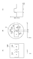
도 1은 일 실시 형태에 따른 고체 촬상 장치의 개략 구성을 나타내는 평면도이다.
도 2는 도 1의 일부분을 확대하여 나타내는 도면이다.
도 3은 일 실시 형태에 따른 고체 촬상 장치의 제조 방법에 있어서 사용되는 포토마스크(photomask)의 패턴의 형상을 나타내는 개략도이다.
도 4는 포토마스크의 패턴의 다른 형상을 나타내는 개략도이다.
도 5는 포토마스크의 패턴의 다른 형상을 나타내는 개략도이다.
도 6은 비교예에 따른 포토마스크의 패턴의 형상을 나타내는 개략도이다.
도 7은 다른 비교예에 따른 포토마스크의 패턴의 형상을 나타내는 개략도이다. 1 is a plan view showing a schematic configuration of a solid-state imaging device according to an embodiment.
Fig. 2 is an enlarged view of a portion of Fig. 1. Fig.
3 is a schematic view showing the shape of a pattern of a photomask used in the method of manufacturing the solid-state imaging device according to the embodiment.
4 is a schematic view showing another shape of the pattern of the photomask.
5 is a schematic view showing another shape of the pattern of the photomask.
6 is a schematic view showing the shape of a pattern of a photomask according to a comparative example.
7 is a schematic view showing the shape of a pattern of a photomask according to another comparative example.
이하, 첨부 도면을 참조하여, 본 발명의 바람직한 실시 형태에 대해 상세하게 설명한다. 또한, 설명에 있어서, 동일 요소 또는 동일 기능을 가지는 요소에는, 동일 부호를 이용하는 것으로 하고, 중복하는 설명은 생략한다. Hereinafter, preferred embodiments of the present invention will be described in detail with reference to the accompanying drawings. In the description, the same reference numerals are used for the same elements or elements having the same function, and a duplicate description will be omitted.
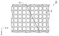
먼저, 도 1 및 도 2를 참조하여, 본 실시 형태에 따른 고체 촬상 장치(1)의 구성을 설명한다. 도 1은 고체 촬상 장치(1)의 개략 구성을 나타내는 평면도이다. 도 2는 도 1에 있어서의 사각형 RII의 내부를 확대하여 나타내는 도면이다. First, the configuration of the solid-state imaging device 1 according to the present embodiment will be described with reference to Figs. 1 and 2. Fig. 1 is a plan view showing a schematic configuration of a solid-state image pickup device 1. Fig. Fig. 2 is an enlarged view of the inside of the rectangle RII in Fig. 1. Fig.
도 1에 도시되는 것처럼, 고체 촬상 장치(1)는 수직 전송부(수광부)(2), 수평 전송부(3), 출력부(4) 및 본딩 패드(5)를 구비하고 있다. 고체 촬상 장치(1)는, 후술하는 것처럼, TDI 구동이 가능한 고체 촬상 장치이다. 1, the solid-state image pickup device 1 includes a vertical transfer section (light receiving section) 2, a
수직 전송부(2)는 반도체 기판상에, 복수(도 1에 도시되는 예에서는 2개)의 패턴(2A, 2B)이, 경계(S)에서 Y축 방향(제1 방향)으로 서로 이어지도록 노광되어 형성되어 있다. 도 2에 도시되는 것처럼, 수직 전송부(2)는 Y축 방향과, Y축 방향에 직교하는 X축 방향(제2 방향)으로 2차원 모양으로 배열된 복수의 화소(6)를 가지고 있다. 화소(6)는, 각각, 수직 전송부(2)에 입사되는 광을 받아, 수광 강도에 따른 양의 전하를 발생한다.The
복수의 화소(6) 중, X축 방향으로 배열된 복수의 화소(6)는, 화소 열을 구성한다. 수직 전송부(2)는 화소 열마다, 전하를 X축 방향의 플러스 방향으로 전송한다. 수직 전송부(2)는 화소(6)의 상방에 있어서 Y축 방향으로 평행하게 연장되는 복수의 전극(도시하지 않음)을 가지고 있다. 수직 전송부(2)는, 이 전극의 전위를 변화시켜서, 전극의 하방에 위치하는 반도체층의 포텐셜의 깊이를 변화시킴으로써, 전하를 전송한다. 특히, 고체 촬상 장치(1)가 TDI 구동되는 경우에는, 수직 전송부(2)는, X축 방향으로 이동하는 촬상 대상물의 이동 속도와 같은 속도로, 전하를 X축 방향으로 전송한다. 수직 전송부(2)는, 전하를, 최종적으로 수평 전송부(3) 까지 전송한다. Among the plurality of
수직 전송부(2)의 패턴(2A)과 패턴(2B)이 서로 이어지는 경계(S)는, X축 방향과 Y축 방향에 교차하는 방향으로 연장되는 1개 이상의 선분 위를 따라서 위치하고 있다. 특히, 본 실시 형태에서는, 경계(S)는, X축 방향과 Y축 방향 모두에 교차하는 하나의 선분을 따라서, 직선 모양으로 마련되어 있다. 또한, 패턴(2A)과 패턴(2B)은, 경계(S)의 근방에 있어서, 서로 겹치는 영역을 가지고 있어도 좋다. The boundary S between the
수평 전송부(3)는 수직 전송부(2)로부터 전송된 전하를, Y축 방향으로 전송한다. 수평 전송부(3)는 수직 전송부(2)와 마찬가지로 전극(도시하지 않음)을 가지고 있다. 수평 전송부(3)는, 수직 전송부(2)에 있어서의 전하의 전송과 마찬가지로, 전극의 전위를 변화시켜서, 전극의 하방에 위치하는 반도체층의 포텐셜의 깊이를 변화시킴으로써, 전하를 전송한다. The
출력부(4)는 수평 전송부(3)로부터 전송된 전하를, 그 전하량에 따른 전압으로 변환하여 출력한다. 출력부(4)로서는, 예를 들면 플로팅·디퓨전·앰프를 사용할 수 있다. The
본딩 패드(5)는, 수직 전송부(2) 및 수평 전송부(3)에 있어서의 전하의 전송을 위해서 사용되는 전극에, 고체 촬상 장치(1)의 외부로부터 전위를 주기 위해서 사용된다. 본딩 패드(5)는, 그 외의 목적, 예를 들면 출력부(4)로부터 출력되는 전압 신호를 취출(取出)하기 위해 사용되어도 된다. The
다음으로, 본 실시 형태에 따른 고체 촬상 장치의 제조 방법에 대해 설명한다. 이 고체 촬상 장치의 제조 방법은, 반도체 기판상에 복수의 패턴을 서로 이어지도록 하여 노광하여 수광부를 형성하는 스텝을 구비하고 있다. Next, a manufacturing method of the solid-state imaging device according to the present embodiment will be described. The manufacturing method of the solid-state imaging device includes a step of forming a light-receiving portion by exposing a plurality of patterns on a semiconductor substrate so as to be connected to each other.
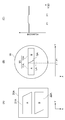
먼저, 도 3을 참조하여, 노광에 사용되는 포토마스크의 마스크 패턴의 바람직한 형상에 대해 설명한다. 도 3 (A)에, 수광부의 형성을 위한 노광에 있어서 사용되는 포토마스크의 형상의 일례를 나타낸다. 포토마스크(20A)는, 평면에서 볼 때사다리꼴 형상의 마스크 패턴(21A) 및 마스크 패턴(22A)을 가지고 있다. First, with reference to FIG. 3, a preferable shape of a mask pattern of a photomask used for exposure will be described. 3 (A) shows an example of the shape of a photomask used in exposure for forming a light receiving portion. The
도 3 (B)에, 포토마스크(20A)를 이용하여 노광을 행했을 경우의 웨이퍼 W(반도체 기판)에 있어서의 패턴의 배치를 나타낸다. 웨이퍼 W에 있어서, 패턴(11A)과 패턴(12A)이, 경계(SA)를 통해서, Y축 방향으로 서로 이어져 있다. 패턴(11A)과 패턴(12A)이 서로 이어져서, 고체 촬상 장치(1A)를 형성한다. 패턴(11A)은 마스크 패턴(21A)에 의해 노광되는 패턴이다. 패턴(12A)은 마스크 패턴(22A)에 의해 노광되는 패턴이다. 경계(SA)는 X축 방향과 Y축 방향에 교차하는 방향으로 연장되는 선분 위를 따라서 위치하고 있다. 특히, 도 3 (B)에 도시한 경계(SA)는, X축 방향을 따라서 연장되는 1개의 직선 LA에 대해서, 1지점에서만 교차하고 있다. Fig. 3 (B) shows the arrangement of the patterns in the wafer W (semiconductor substrate) when exposure is performed using the
도 3 (C)에, 고체 촬상 장치(1A)에, 균일한 강도의 광을 입사시켰을 경우의 출력 신호 강도의 Y축에 대한 변화를 나타낸다. 고체 촬상 장치(1A)에 입사되는 광의 강도는 고르기 때문에, 출력 신호 강도는 일정하게 되는 것이 바람직하다. 고체 촬상 장치(1A)의 경우에는, 패턴(11A)과 패턴(12A)의 위치 맞춤의 불일치 등에 의해, 출력 신호 강도는, 경계(SA)의 일단의 Y좌표 y1A와, 경계(SA)의 타단의 Y좌표 y2A의 사이에서, 다른 부분과 비교해서 약간의 차가 생겨 있다. 이 차는 경계(SA)상에 위치하는 화소(6)에 있어서는, 패턴(11A)과 패턴(12A)의 위치 맞춤의 불일치 등의 영향에 의해, 경계(SA)상에 위치하지 않는 화소(6)와 비교하여, 입사광의 강도와, 발생하는 전하의 양 사이의 관계가 다른 것에 기인한다. Y좌표 y1A와 Y좌표 y2A 사이의 영역에서는, X축 방향을 따른 화소 열에는, 경계(SA)상에 위치하는 화소(6)가 포함되는데 비해, Y좌표가 y1A보다 작은 영역, 또는 Y좌표가 y2A보다 큰 영역에서는, X축 방향을 따른 화소 열에는, 경계(SA)상에 위치하는 화소(6)는 포함되지 않는다. 이 때문에, 도 3 (C)에 도시한 것처럼, Y좌표 y1A와 Y좌표 y2A 사이의 영역에서는, 다른 영역과 비교하여, 출력 신호 강도의 특성에 약간의 차가 생긴다. 그렇지만, 도 3 (C)에 도시한 출력 신호 강도의 Y좌표에 따른 차는 충분히 작아서, 실용상, 출력 신호 강도는 충분히 균일한 것으로 되어 있다. Fig. 3 (C) shows the change in the output signal intensity with respect to the Y-axis when light of uniform intensity is incident on the solid-state
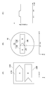
다음으로, 도 4를 참조하여, 노광에 사용되는 포토마스크의 마스크 패턴의 다른 바람직한 형상에 대해 설명한다. 도 4 (A)에, 포토마스크의 형상의 일례를 나타낸다. 포토마스크(20B)는 5각형 형상의 마스크 패턴(21B) 및 마스크 패턴(22B)을 가지고 있다. Next, another preferable shape of the mask pattern of the photomask used for exposure will be described with reference to Fig. Fig. 4 (A) shows an example of the shape of the photomask. The
도 4 (B)에, 포토마스크(20B)를 이용하여 노광을 행했을 경우의 웨이퍼 W에 있어서의 패턴의 배치를 나타낸다. 웨이퍼 W에 있어서, 패턴(11B)과 패턴(12B)이, 경계(SA)를 통해서, Y축 방향으로 서로 이어져 있다. 패턴(11B)과 패턴(12B)이 서로 이어져서, 고체 촬상 장치(1B)를 형성한다. 패턴(11B)은 마스크 패턴(21B)에 의해 노광되는 패턴이다. 패턴(12B)은 마스크 패턴(22B)에 의해 노광되는 패턴이다. 경계(SB)는, 하나의 모서리에 의해서 구획된 두 개의 부분을 가지는 꺾인 선으로서 마련되어 있다. 두 개의 부분은, 각각, X축 방향과 Y축 방향에 교차하는 방향으로 연장되는 2개의 선분의 각각을 따라서 위치하고 있다. 도 4 (B)에 도시한 경계(SB)는, X축 방향을 따라서 연장되는 1개의 직선 LB에 대해서, 2지점에서 교차하고 있다. 경계(SB) 중, Y좌표가 최소가 되는 점의 Y좌표는 y1B이고, Y좌표가 최대가 되는 점의 좌표는 y2B이다. Fig. 4 (B) shows the arrangement of the patterns on the wafer W when exposure is performed using the
도 4 (C)에, 고체 촬상 장치(1B)에, 균일한 강도의 광을 입사시켰을 경우의 출력 신호 강도의 Y축에 대한 변화를 나타낸다. 고체 촬상 장치(1B)의 경우에는, 패턴(11B)과 패턴(12B)의 위치 맞춤의 불일치 등에 의해, 출력 신호 강도는, Y좌표 y1B와 Y좌표 y2B의 사이에서, 다른 부분과 비교해서 약간의 차가 생겨 있다. 이 차는, 도 3 (C)에 도시한, Y좌표 y1A와 Y좌표 y2A 사이의 영역과 그 외의 영역의 출력 신호 강도의 차보다는 약간 크다고는 해도, 충분히 작은 것이어서, 실용상, 출력 신호 강도는 충분히 균일한 것으로 되어 있다. Fig. 4 (C) shows the change in the output signal intensity with respect to the Y-axis when light of uniform intensity is incident on the solid-state
또한, 도 3에 도시한 고체 촬상 장치(1A)의 패턴(11A, 12A)과, 도 4에 도시한 고체 촬상 장치(1B)의 패턴(11B, 12B)의 경계(SB)의 형상을 비교하여, 그것들의 특징에 대해 이하에 기술한다. 도 3 (B)에 도시한 것처럼, 직선 LA를 따른 화소 열은 경계(SA)와 1지점에서 교차하는데 비해, 도 4 (B)에 도시한 것처럼, 직선 LB를 따른 화소 열은 경계(SB)와 2지점에서 교차한다. 이 때문에, 고체 촬상 장치(1A)는, 고체 촬상 장치(1B)와 비교하면, 경계상에 위치하는 화소의 수가 적기 때문에, 출력 신호 강도가 한층 균일한 것이 되는 점에서는 유리하다. 한편, 경계를, X축에 대해 일정한 각도로 경사진 1개 이상의 선분에 따른 직선 또는 꺾인 선으로 하는 경우, 도 4 (A)에 나타낸 포토마스크(20B)는, 도 3 (A)에 나타낸 포토마스크(20A) 보다도 면적을 작게 할 수 있는 점에서 유리하다. The shapes of the
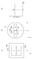
마스크 패턴의 수 및 고체 촬상 장치의 수직 전송부에 있어서의 패턴의 수는, 각각 2개로 한정되는 것은 아니다. 마스크 패턴의 수와 고체 촬상 장치의 패턴의 수를, 다른 수로 해도 된다. 도 5를 참조하여, 노광에 사용되는 포토마스크의 마스크 패턴의, 또 다른 바람직한 형상에 대해 설명한다. 도 5 (A)에, 포토마스크의 형상의 일례를 나타낸다. 포토마스크(20C)는 사다리꼴 형상의 마스크 패턴(21C), 평행 사변형 형상의 마스크 패턴(22C) 및 사다리꼴 형상의 마스크 패턴(23C)을 가지고 있다. The number of mask patterns and the number of patterns in the vertical transfer portion of the solid-state imaging device are not limited to two, respectively. The number of mask patterns and the number of patterns of the solid-state imaging device may be different from each other. Another preferred shape of the mask pattern of the photomask used for exposure will be described with reference to Fig. Fig. 5 (A) shows an example of the shape of the photomask. The
도 5 (B)에, 포토마스크(20C)를 이용하여 노광을 행했을 경우의 웨이퍼 W에 있어서의 패턴의 배치를 나타낸다. 웨이퍼 W에 있어서, 패턴(11C, 12C, 13C, 14C, 15C)이, 각각 경계(SC1, SC2, SC3, SC4)를 통해서, Y축 방향으로 서로 이어져 있다. 경계(SC1~SC4)는 각각 X축 방향과 Y축 방향의 양쪽에 대해서 각각 일정한 각도를 이루는 선분을 따라서 배치되어 있다. 경계(SC1, SC2, SC3, SC4)는, 각각의 일단의 Y좌표가 y1C, y3C, y5C, y7C이고, 각각의 타단의 Y좌표가 y2C, y4C, y6C, y8C이다. 경계(SC1)는, X축 방향을 따라서 연장되는 1개의 직선 LC에 대해서, 1지점에서 교차하고 있다. 경계(SC2~SC4)도 마찬가지로, X축 방향을 따라서 연장되는 직선에 대해서 1지점에서 교차한다. Fig. 5B shows the arrangement of the patterns on the wafer W when exposure is performed using the
패턴(11C, 12C, 13C, 14C, 15C)이 서로 이어져서, 고체 촬상 장치(1C)를 형성한다. 패턴(11C)은 마스크 패턴(21C)에 의해 노광된다. 패턴(12C, 13C, 14C)은, 마스크 패턴(22C)에 의해 노광된다. 패턴(15C)은 마스크 패턴(23C)에 의해 노광된다. 패턴(12C, 13C, 14C)의 노광은, 포토마스크(20C)의 웨이퍼 W에 대한 위치를 바꾸면서 반복 노광을 행함으로써 행해진다. The patterns 11C, 12C, 13C, 14C and 15C are connected to each other to form the solid-state
도 5 (C)에, 고체 촬상 장치(1C)에, 균일한 강도의 광을 입사시켰을 경우의 출력 신호 강도의 Y축에 대한 변화를 나타낸다. 고체 촬상 장치(1C)의 경우에는, 패턴(11C~15C)의 위치 맞춤의 불일치 등에 의해, 출력 신호가, Y좌표 y1C~y2C, Y좌표 y3C~y4C, Y좌표 y5C~y6C, Y좌표 y7C~y8C의 영역에 있어서, 다른 영역과 비교해서 차가 생겨 있다. 그렇지만, 도 5 (C)에 도시한 출력 신호 강도의 Y좌표에 따른 차는 충분히 작아서, 실용상, 출력 신호 강도는 충분히 균일한 것으로 되어 있다. FIG. 5C shows a change in the output signal intensity with respect to the Y-axis when light of uniform intensity is incident on the solid-state
이하, 도 6 및 도 7을 참조하여, 본 발명의 실시 형태에 대한 비교예를 설명한다. 도 6 (A)에, 비교예에 따른 포토마스크의 형상의 일례를 나타낸다. 포토마스크(120D)는 직사각형 형상의 마스크 패턴(121D) 및 마스크 패턴(122D)을 가지고 있다. Hereinafter, a comparative example of the embodiment of the present invention will be described with reference to Figs. 6 and 7. Fig. Fig. 6 (A) shows an example of the shape of the photomask according to the comparative example. The
도 6 (B)에, 포토마스크(120D)를 이용하여 노광을 행했을 경우의 웨이퍼 W에 있어서의 패턴의 배치를 나타낸다. 웨이퍼 W에 있어서, 패턴(111D)과 패턴(112D)이, 경계(SD)를 통해서, Y축 방향으로 서로 이어져 있다. 패턴(111D)과 패턴(112D)이 서로 이어져서, 고체 촬상 장치(101D)를 형성한다. 패턴(111D)은 마스크 패턴(121D)에 의해 노광되는 패턴이다. 패턴(112D)은 마스크 패턴(122D)에 의해 노광되는 패턴이다. 경계(SD)는 X축 방향을 따라서 위치하고 있다. 도 6 (B)에 도시한 경계(SD)는, X축 방향을 따라서 연장되는 1개의 직선 LD와 평행하게 위치하고 있다. 경계(SD)상의 각 점의 Y좌표는 y1D이다.Fig. 6B shows the arrangement of patterns on the wafer W when exposure is performed using the
도 6 (C)에, 고체 촬상 장치(101D)에, 균일한 강도의 광을 입사시켰을 경우의 출력 신호 강도의 Y축에 대한 변화를 나타낸다. 고체 촬상 장치(101D)의 경우에는, 패턴(111D)과 패턴(111D)의 위치 맞춤의 불일치 등에 의해, 출력 신호 강도는, Y좌표 y1D에 있어서, 다른 부분과 비교해서 큰 차가 생겨 있다. 이 차는, 도 3에 도시한, Y좌표가 y1A~y2A의 구간과 그 외의 구간의 출력 신호 강도의 차보다도 현저하게 크다. 이것은, Y좌표가 y1D가 되는 화소 열을 구성하는 화소(6)가, 모두 경계(SD)상에 위치하기 때문에, 다른 위치의 화소(6)와 비교하여 출력 신호 강도의 특성이 다르기 때문이다. FIG. 6C shows a change in the output signal intensity with respect to the Y-axis when light of uniform intensity is incident on the solid-
도 7에 다른 비교예를 나타낸다. 도 7 (A)에, 비교예에 따른 포토마스크의 형상의 일례를 나타낸다. 포토마스크(120E)는 직사각형의 단변 중 한 변을, X축 방향 및 Y축 방향의 양쪽에 교차하는 변 2개와, 이들 변을 접속하고 Y축에 평행한 1개의 변으로 이루어지는 꺾인 선으로 치환한 육각형 형상의 마스크 패턴(121E) 및 마스크 패턴(122E)을 가지고 있다. Fig. 7 shows another comparative example. Fig. 7 (A) shows an example of the shape of the photomask according to the comparative example. The
도 7 (B)에, 포토마스크(120E)를 이용하여 노광을 행했을 경우의 웨이퍼 W에 있어서의 패턴의 배치를 나타낸다. 웨이퍼 W에 있어서, 패턴(111E)과 패턴(112E)이, 경계(SA)를 통해서, Y축 방향으로 서로 이어져 있다. 패턴(111E)과 패턴(112E)이 서로 이어져서, 고체 촬상 장치(101E)를 형성한다. 패턴(111E)은 마스크 패턴(121E)에 의해 노광되는 패턴이다. 패턴(112E)은 마스크 패턴(122E)에 의해 노광되는 패턴이다. 경계(SE)는 X축 방향 및 Y축 방향의 양쪽에 교차하는 부분(SE1, SE3)과, Y축 방향에 평행한 부분(SE2)으로 이루어진다. 도 6 (B)에 도시한 경계(SE)는, X축 방향을 따라서 연장되는 1개의 직선 LE와 3지점에서 교차하고 있다. 경계(SE)상의 각 점의 Y좌표는 y1D이다. Fig. 7B shows the arrangement of the patterns on the wafer W when exposure is performed using the
도 7 (C)에, 고체 촬상 장치(101E)에, 균일한 강도의 광을 입사시켰을 경우의 출력 신호 강도의 Y축에 대한 변화를 나타낸다. 고체 촬상 장치(101E)의 경우에는, 패턴(111E)과 패턴(112E)의 위치 맞춤의 불일치 등에 의해, 출력 신호 강도는 Y좌표 y1E~y2E에 있어서, 다른 부분과 비교해서 큰 차가 생겨 있다. 이 차는, 도 4에 도시한, Y좌표가 y1B~y2B의 구간과 그 외의 구간의 출력 신호 강도의 차보다도 크다. 이것은, 경계(SE)에, Y축 방향에 평행한 부분(SE2)이 존재함으로써, Y좌표가 y1E~y2E의 구간에 위치하는 화소 열을 구성하는 화소(6) 중, 부분(SE2)상에 위치하는 것이 존재함으로써, 경계(SE)상에 위치하는 화소(6)의 수가 증가해 있기 때문에 있다. 이와 같이, 패턴의 경계상에, Y축 방향에 평행한 부분을 마련하는 것은, 출력 신호 강도의 특성을 불균일한 것으로 하기 때문에, 바람직하지 않다. Fig. 7C shows a change in the output signal intensity with respect to the Y-axis when light of uniform intensity is incident on the solid-
본 발명의 실시 형태에 따른 고체 촬상 장치(1)에서는, 수직 전송부(2)는 복수의 패턴(11, 12)이 제1 방향으로 서로 이어지도록 노광되어 형성되어 있다. 이 수직 전송부(2)는, X축 방향과 이것에 직교하는 Y축 방향으로 2차원 모양으로 배열된 복수의 화소(6)를 가진다. 복수의 화소(6) 중, X축 방향으로 배열된 복수의 화소로 이루어지는 화소 열마다, 전하가 X축 방향으로 전송된다. 한편, 복수의 패턴이 서로 이어지는 경계는, X축 방향과 Y축 방향에 교차하는 방향으로 연장되는 1개 이상의 선분 위를 따라서 위치하고 있다. 따라서 전하가 전송되는 X축 방향과, 화소 열을 구성하는 복수의 화소(6)의 배열 방향은 다르다. 이 때문에, 복수의 패턴의 경계의 영향이 화소(6)의 특정 열에만 집중되지 않고, 복수의 화소 열로 분산된다. 이 결과, 복수의 패턴의 경계 부분에 있어서, 화소 열로부터의 출력 신호의 불균일성이 완화되어, 출력 신호를 충분히 균일한 것으로 할 수 있다.In the solid-state imaging device 1 according to the embodiment of the present invention, the
복수의 패턴(11, 12)이 서로 이어지는 경계가, X축 방향으로 연장되는 1개의 직선에 대해서, 1지점에서만 교차하고 있는 경우에는, Y축 방향을 따라서 전하의 전송이 행해지는 화소 열과 복수의 패턴(11, 12)의 경계가 교차하는 지점이 1지점이 된다. 이 때문에, 복수의 패턴의 경계에 의한 출력 신호의 불균일성을 한층 완화하여, 출력 신호를 한층 균일한 것으로 할 수 있다. When the boundary between the plurality of patterns 11 and 12 intersects one straight line extending in the X-axis direction only at one point, a pixel column in which electric charges are transferred along the Y- The point where the boundaries of the patterns 11 and 12 intersect is one point. Therefore, the non-uniformity of the output signal due to the boundaries of the plurality of patterns is further alleviated, and the output signal can be made more uniform.
고체 촬상 장치(1)가 TDI 구동이 가능한 경우에는, 일정 속도로 이동하는 물체를 촬영하는 경우에, 물체의 이동 방향을 X축 방향으로 하여, 고체 촬상 장치를 TDI 구동함으로써, 출력 신호를 충분히 균일한 상태로 하여, 이 이동하는 물체의 촬영을 행할 수 있다.When the solid-state imaging device 1 is capable of TDI driving, when the object moving at a constant speed is photographed, the solid-state imaging device is TDI-driven with the moving direction of the object in the X-axis direction, So that the moving object can be photographed.
본 실시 형태는, 제1 방향과 제1 방향에 직교하는 제2 방향으로 2차원 모양으로 배열된 복수의 화소를 가지고, 복수의 화소 중, 제2 방향으로 배열된 복수의 화소로 이루어지는 화소 열마다, 전하를 제2 방향으로 전송하는 수광부를 구비하는 고체 촬상 장치의 제조 방법으로서, 반도체 기판상에 복수의 패턴을 제1 방향으로 서로 이어지도록 노광하여 수광부를 형성하는 스텝을 구비하고, 수광부를 형성하는 상기 스텝에서는, 복수의 패턴이 서로 이어지는 경계를, 제1 방향과 제2 방향에 교차하는 방향으로 연장되는 1개 이상의 선분 위를 따라서 위치시킨다. The present embodiment is a liquid crystal display device having a plurality of pixels arranged in a two-dimensional shape in a first direction and in a second direction orthogonal to the first direction, and in each pixel column made up of a plurality of pixels arranged in the second direction And a step of forming a light receiving portion by exposing the plurality of patterns so as to be connected to each other in the first direction on the semiconductor substrate so as to form a light receiving portion The boundary where a plurality of patterns are connected to each other is positioned along one or more line segments extending in a direction intersecting the first direction and the second direction.
이상, 본 발명의 바람직한 실시 형태에 대해 설명했지만, 본 발명은 상술한 실시 형태로 한정되는 것은 아니다. 패턴의 경계의 형상은, 패턴의 경계가 상기 제1 방향과 상기 제2 방향에 교차하는 방향으로 연장되는 1개 이상의 선분 위를 따라서 위치하고 있으면, 도 3 ~ 도 5에 도시한 것으로 한정되지 않고, 어떠한 것이라도 좋다. 또, 본 발명의 고체 촬상 장치는, 전하를 전송함으로써, 비닝을 행하여 인접하는 복수의 화소를 단위 화소로서 취급하는 것이어도 좋다. The preferred embodiments of the present invention have been described above, but the present invention is not limited to the above-described embodiments. The shape of the boundary of the pattern is not limited to that shown in Figs. 3 to 5 as long as the boundary of the pattern is located along one or more line segments extending in the direction crossing the first direction and the second direction, Anything is good. Further, the solid-state imaging device of the present invention may be a structure in which a plurality of pixels adjacent to each other are treated as a unit pixel by carrying out the binning by transferring electric charges.
[산업상의 이용 가능성][Industrial Availability]
본 발명은 고체 촬상 장치 및 고체 촬상 장치의 제조 방법에 이용할 수 있다. INDUSTRIAL APPLICABILITY The present invention can be used in a solid-state imaging device and a manufacturing method of a solid-state imaging device.
1 … 고체 촬상 장치,
2 … 수직 전송부(수광부),
2A, 2B, 11A, 12A, 11B, 12B, 11C~15C … 패턴,
3 … 수평 전송부,
6 … 화소,
W … 웨이퍼(반도체 기판). One … Solid state imaging device, 2 ... A vertical transfer unit (light-receiving unit)
2A, 2B, 11A, 12A, 11B, 12B, 11C to 15C, pattern,
3 ... Horizontal transfer part, 6 ... Pixel,
W ... Wafer (semiconductor substrate).
Claims (4)
상기 수광부는, 상기 제1 방향과 상기 제1 방향에 직교하는 제2 방향으로 2차원 모양으로 배열된 복수의 화소를 가지고, 상기 복수의 화소 중, 상기 제2 방향으로 배열된 복수의 화소로 이루어지는 화소 열마다, 전하를 제2 방향으로 전송하고 있고,
상기 수광부에서는, 상기 복수의 패턴이 서로 이어지는 경계가, 상기 제1 방향과 상기 제2 방향에 교차하는 방향으로 연장되는 1개 이상의 선분 위를 따라서 위치하고 있는 고체 촬상 장치.1. A solid-state imaging device comprising: a light-receiving portion formed on a semiconductor substrate by exposure so that a plurality of patterns are connected to each other in a first direction,
Wherein the light receiving section has a plurality of pixels arranged in a two-dimensional shape in the first direction and in a second direction orthogonal to the first direction, and a plurality of pixels arranged in the second direction among the plurality of pixels For each pixel column, the charge is transferred in the second direction,
Wherein a boundary between the plurality of patterns is located along one or more line segments extending in a direction crossing the first direction and the second direction in the light receiving section.
상기 복수의 패턴이 서로 이어지는 상기 경계는, 상기 제2 방향으로 연장되는 1개의 직선에 대해서, 한 지점에서만 교차하는 고체 촬상 장치.The method according to claim 1,
The boundary where the plurality of patterns are connected to each other intersects only one straight line extending in the second direction at only one point.
TDI 구동이 가능한 고체 촬상 장치.The method according to claim 1 or 2,
A solid-state imaging device capable of TDI drive.
상기 수광부는, 상기 제1 방향과 상기 제1 방향에 직교하는 제2 방향으로 2차원 모양으로 배열된 복수의 화소를 가지고, 상기 복수의 화소 중, 상기 제2 방향으로 배열된 복수의 화소로 이루어지는 화소 열마다, 전하를 제2 방향으로 전송하고 있고,
상기 수광부에서는, 상기 복수의 패턴이 서로 이어지는 경계가, 상기 제1 방향과 상기 제2 방향에 교차하는 방향으로 연장되는 1개 이상의 선분 위를 따라서 위치하고 있는 고체 촬상 장치의 제조 방법.A step of forming a light receiving portion by exposing a plurality of patterns on a semiconductor substrate so as to be connected to each other in a first direction,
Wherein the light receiving section has a plurality of pixels arranged in a two-dimensional shape in the first direction and in a second direction orthogonal to the first direction, and a plurality of pixels arranged in the second direction among the plurality of pixels For each pixel column, the charge is transferred in the second direction,
Wherein a boundary between the plurality of patterns is located along one or more line segments extending in a direction intersecting the first direction and the second direction in the light receiving section.
Applications Claiming Priority (3)
| Application Number | Priority Date | Filing Date | Title |
|---|---|---|---|
| JPJP-P-2013-025620 | 2013-02-13 | ||
| JP2013025620A JP6110154B2 (en) | 2013-02-13 | 2013-02-13 | Solid-state imaging device and method for manufacturing solid-state imaging device |
| PCT/JP2014/053185 WO2014126100A1 (en) | 2013-02-13 | 2014-02-12 | Solid-state image pickup device and method for manufacturing solid-state image pickup device |
Publications (2)
| Publication Number | Publication Date |
|---|---|
| KR20150120334A true KR20150120334A (en) | 2015-10-27 |
| KR102128639B1 KR102128639B1 (en) | 2020-06-30 |
Family
ID=51354099
Family Applications (1)
| Application Number | Title | Priority Date | Filing Date |
|---|---|---|---|
| KR1020157017814A KR102128639B1 (en) | 2013-02-13 | 2014-02-12 | Solid-state image pickup device and method for manufacturing solid-state image pickup device |
Country Status (7)
| Country | Link |
|---|---|
| US (1) | US9749561B2 (en) |
| EP (1) | EP2958147B1 (en) |
| JP (1) | JP6110154B2 (en) |
| KR (1) | KR102128639B1 (en) |
| CN (1) | CN104995735B (en) |
| TW (1) | TWI652809B (en) |
| WO (1) | WO2014126100A1 (en) |
Families Citing this family (1)
| Publication number | Priority date | Publication date | Assignee | Title |
|---|---|---|---|---|
| TW202031539A (en) * | 2019-02-25 | 2020-09-01 | 先進光電科技股份有限公司 | Action vehicle auxiliary system |
Citations (5)
| Publication number | Priority date | Publication date | Assignee | Title |
|---|---|---|---|---|
| JP2000101061A (en) | 1998-09-21 | 2000-04-07 | Hamamatsu Photonics Kk | Solid-state image sensing device |
| JP2001077343A (en) * | 1999-09-01 | 2001-03-23 | Sony Corp | Method and device for manufacture of ccd image sensing element |
| JP2003347539A (en) | 2002-05-27 | 2003-12-05 | Hamamatsu Photonics Kk | Solid-state image pickup device and its array |
| JP2010093331A (en) * | 2008-10-03 | 2010-04-22 | Mitsubishi Electric Corp | Image sensor and driving method therefor |
| US20130057739A1 (en) * | 2011-02-24 | 2013-03-07 | Teledyne Dalsa, Inc. | Continuous clocking mode for tdi binning operation of ccd image sensor |
Family Cites Families (12)
| Publication number | Priority date | Publication date | Assignee | Title |
|---|---|---|---|---|
| US5298761A (en) * | 1991-06-17 | 1994-03-29 | Nikon Corporation | Method and apparatus for exposure process |
| US6048785A (en) * | 1997-06-16 | 2000-04-11 | Advanced Micro Devices, Inc. | Semiconductor fabrication method of combining a plurality of fields defined by a reticle image using segment stitching |
| JP2003179221A (en) | 2001-12-11 | 2003-06-27 | Mitsubishi Electric Corp | Manufacturing method and structure of linear image sensor |
| JP2003280173A (en) | 2002-03-26 | 2003-10-02 | Canon Inc | Mask for lithography, method for manufacturing semiconductor device using the same, and the semiconductor device |
| WO2007014293A1 (en) * | 2005-07-25 | 2007-02-01 | The Regents Of The University Of California | Digital imaging system and method to produce mosaic images |
| JP5214904B2 (en) * | 2007-04-12 | 2013-06-19 | ルネサスエレクトロニクス株式会社 | Manufacturing method of solid-state imaging device |
| JP4462299B2 (en) * | 2007-07-17 | 2010-05-12 | ソニー株式会社 | Imaging apparatus, image processing method, and computer program |
| US7737390B2 (en) * | 2008-01-14 | 2010-06-15 | Tower Semiconductor, Ltd. | Horizontal row drivers for CMOS image sensor with tiling on three edges |
| JP5418810B2 (en) | 2008-02-14 | 2014-02-19 | ソニー株式会社 | Clamp control method, clamp correction device, image sensor, and electronic device |
| US8866890B2 (en) * | 2010-11-05 | 2014-10-21 | Teledyne Dalsa, Inc. | Multi-camera |
| US20120113213A1 (en) * | 2010-11-05 | 2012-05-10 | Teledyne Dalsa, Inc. | Wide format sensor |
| JP5917883B2 (en) * | 2011-11-02 | 2016-05-18 | 浜松ホトニクス株式会社 | Solid-state imaging device |
-
2013
- 2013-02-13 JP JP2013025620A patent/JP6110154B2/en active Active
-
2014
- 2014-02-12 US US14/766,788 patent/US9749561B2/en active Active
- 2014-02-12 KR KR1020157017814A patent/KR102128639B1/en active IP Right Grant
- 2014-02-12 EP EP14751421.0A patent/EP2958147B1/en active Active
- 2014-02-12 WO PCT/JP2014/053185 patent/WO2014126100A1/en active Application Filing
- 2014-02-12 CN CN201480008752.0A patent/CN104995735B/en active Active
- 2014-02-13 TW TW103104780A patent/TWI652809B/en active
Patent Citations (5)
| Publication number | Priority date | Publication date | Assignee | Title |
|---|---|---|---|---|
| JP2000101061A (en) | 1998-09-21 | 2000-04-07 | Hamamatsu Photonics Kk | Solid-state image sensing device |
| JP2001077343A (en) * | 1999-09-01 | 2001-03-23 | Sony Corp | Method and device for manufacture of ccd image sensing element |
| JP2003347539A (en) | 2002-05-27 | 2003-12-05 | Hamamatsu Photonics Kk | Solid-state image pickup device and its array |
| JP2010093331A (en) * | 2008-10-03 | 2010-04-22 | Mitsubishi Electric Corp | Image sensor and driving method therefor |
| US20130057739A1 (en) * | 2011-02-24 | 2013-03-07 | Teledyne Dalsa, Inc. | Continuous clocking mode for tdi binning operation of ccd image sensor |
Also Published As
| Publication number | Publication date |
|---|---|
| EP2958147B1 (en) | 2019-06-12 |
| TWI652809B (en) | 2019-03-01 |
| US20150365613A1 (en) | 2015-12-17 |
| WO2014126100A1 (en) | 2014-08-21 |
| JP6110154B2 (en) | 2017-04-05 |
| KR102128639B1 (en) | 2020-06-30 |
| CN104995735A (en) | 2015-10-21 |
| JP2014154821A (en) | 2014-08-25 |
| EP2958147A1 (en) | 2015-12-23 |
| US9749561B2 (en) | 2017-08-29 |
| EP2958147A4 (en) | 2016-09-28 |
| TW201444072A (en) | 2014-11-16 |
| CN104995735B (en) | 2018-06-19 |
Similar Documents
| Publication | Publication Date | Title |
|---|---|---|
| US20160300878A1 (en) | Imaging device and imaging system | |
| US10636822B2 (en) | Photoelectric conversion element and solid-state image capturing device | |
| TWI553845B (en) | Solid-state imaging device | |
| CN105762162A (en) | Solid-state imaging device, camera and design method for solid-state imaging device | |
| US20190252449A1 (en) | Imaging element and imaging apparatus | |
| KR101445332B1 (en) | Display apparatus | |
| CN111684600A (en) | Pixel array for a camera, camera and light travel time camera system with such a camera | |
| JP5870104B2 (en) | CCD sensor having a plurality of contact patterns | |
| KR20160082682A (en) | Charge-coupled device, manufacturing method therefor, and solid-state imaging element | |
| JP7209170B2 (en) | Photodetector and imaging device | |
| KR20150120334A (en) | Solid-state image pickup device and method for manufacturing solid-state image pickup device | |
| TWI537805B (en) | Capacitive touch panel with single sensing layer | |
| US10068940B2 (en) | Imaging apparatus with focus-ranging precision in one direction due to saturated photoelectric conversion elements located adjacent to each other | |
| US10199418B2 (en) | Semiconductor photodetection device | |
| US9635293B2 (en) | Solid-state imaging device | |
| CN107507843B (en) | Pixel structure and X-ray image sensor | |
| JP5052421B2 (en) | TDI image sensor and driving method thereof | |
| JP5836376B2 (en) | CCD sensor having a plurality of contact patterns | |
| JP5943808B2 (en) | Imaging system using TDI linear image sensor and driving method thereof | |
| JP2019012820A (en) | Optical detector and imaging apparatus | |
| JP2016025187A (en) | Solid state imaging apparatus and method for driving the same, and electronic apparatus | |
| JPS60157251A (en) | Infrared-ray detection element | |
| JP2015230958A (en) | Solid-state image pickup device | |
| JP2015041721A (en) | Semiconductor device | |
| JPH04262575A (en) | Solid state image sensor |
Legal Events
| Date | Code | Title | Description |
|---|---|---|---|
| E902 | Notification of reason for refusal | ||
| E701 | Decision to grant or registration of patent right | ||
| GRNT | Written decision to grant |