KR20150108994A - Display device and method for driving the same - Google Patents
Display device and method for driving the same Download PDFInfo
- Publication number
- KR20150108994A KR20150108994A KR1020140031736A KR20140031736A KR20150108994A KR 20150108994 A KR20150108994 A KR 20150108994A KR 1020140031736 A KR1020140031736 A KR 1020140031736A KR 20140031736 A KR20140031736 A KR 20140031736A KR 20150108994 A KR20150108994 A KR 20150108994A
- Authority
- KR
- South Korea
- Prior art keywords
- data
- scan
- pixels
- data signal
- signal
- Prior art date
- Legal status (The legal status is an assumption and is not a legal conclusion. Google has not performed a legal analysis and makes no representation as to the accuracy of the status listed.)
- Withdrawn
Links
- 238000000034 method Methods 0.000 title claims abstract description 46
- 238000010586 diagram Methods 0.000 description 14
- 239000011521 glass Substances 0.000 description 13
- 230000009977 dual effect Effects 0.000 description 7
- 239000003990 capacitor Substances 0.000 description 6
- 230000001360 synchronised effect Effects 0.000 description 5
- 239000011159 matrix material Substances 0.000 description 2
- 238000012986 modification Methods 0.000 description 2
- 230000004048 modification Effects 0.000 description 2
- 238000002834 transmittance Methods 0.000 description 2
- 230000007423 decrease Effects 0.000 description 1
- 230000000694 effects Effects 0.000 description 1
- 239000004973 liquid crystal related substance Substances 0.000 description 1
- 238000005215 recombination Methods 0.000 description 1
- 230000006798 recombination Effects 0.000 description 1
- 239000010409 thin film Substances 0.000 description 1
Images


Classifications
-
- G—PHYSICS
- G09—EDUCATION; CRYPTOGRAPHY; DISPLAY; ADVERTISING; SEALS
- G09G—ARRANGEMENTS OR CIRCUITS FOR CONTROL OF INDICATING DEVICES USING STATIC MEANS TO PRESENT VARIABLE INFORMATION
- G09G3/00—Control arrangements or circuits, of interest only in connection with visual indicators other than cathode-ray tubes
- G09G3/001—Control arrangements or circuits, of interest only in connection with visual indicators other than cathode-ray tubes using specific devices not provided for in groups G09G3/02 - G09G3/36, e.g. using an intermediate record carrier such as a film slide; Projection systems; Display of non-alphanumerical information, solely or in combination with alphanumerical information, e.g. digital display on projected diapositive as background
- G09G3/003—Control arrangements or circuits, of interest only in connection with visual indicators other than cathode-ray tubes using specific devices not provided for in groups G09G3/02 - G09G3/36, e.g. using an intermediate record carrier such as a film slide; Projection systems; Display of non-alphanumerical information, solely or in combination with alphanumerical information, e.g. digital display on projected diapositive as background to produce spatial visual effects
-
- G—PHYSICS
- G09—EDUCATION; CRYPTOGRAPHY; DISPLAY; ADVERTISING; SEALS
- G09G—ARRANGEMENTS OR CIRCUITS FOR CONTROL OF INDICATING DEVICES USING STATIC MEANS TO PRESENT VARIABLE INFORMATION
- G09G3/00—Control arrangements or circuits, of interest only in connection with visual indicators other than cathode-ray tubes
- G09G3/20—Control arrangements or circuits, of interest only in connection with visual indicators other than cathode-ray tubes for presentation of an assembly of a number of characters, e.g. a page, by composing the assembly by combination of individual elements arranged in a matrix no fixed position being assigned to or needed to be assigned to the individual characters or partial characters
- G09G3/2007—Display of intermediate tones
- G09G3/2018—Display of intermediate tones by time modulation using two or more time intervals
- G09G3/2022—Display of intermediate tones by time modulation using two or more time intervals using sub-frames
-
- G—PHYSICS
- G09—EDUCATION; CRYPTOGRAPHY; DISPLAY; ADVERTISING; SEALS
- G09G—ARRANGEMENTS OR CIRCUITS FOR CONTROL OF INDICATING DEVICES USING STATIC MEANS TO PRESENT VARIABLE INFORMATION
- G09G3/00—Control arrangements or circuits, of interest only in connection with visual indicators other than cathode-ray tubes
- G09G3/20—Control arrangements or circuits, of interest only in connection with visual indicators other than cathode-ray tubes for presentation of an assembly of a number of characters, e.g. a page, by composing the assembly by combination of individual elements arranged in a matrix no fixed position being assigned to or needed to be assigned to the individual characters or partial characters
- G09G3/22—Control arrangements or circuits, of interest only in connection with visual indicators other than cathode-ray tubes for presentation of an assembly of a number of characters, e.g. a page, by composing the assembly by combination of individual elements arranged in a matrix no fixed position being assigned to or needed to be assigned to the individual characters or partial characters using controlled light sources
- G09G3/30—Control arrangements or circuits, of interest only in connection with visual indicators other than cathode-ray tubes for presentation of an assembly of a number of characters, e.g. a page, by composing the assembly by combination of individual elements arranged in a matrix no fixed position being assigned to or needed to be assigned to the individual characters or partial characters using controlled light sources using electroluminescent panels
- G09G3/32—Control arrangements or circuits, of interest only in connection with visual indicators other than cathode-ray tubes for presentation of an assembly of a number of characters, e.g. a page, by composing the assembly by combination of individual elements arranged in a matrix no fixed position being assigned to or needed to be assigned to the individual characters or partial characters using controlled light sources using electroluminescent panels semiconductive, e.g. using light-emitting diodes [LED]
- G09G3/3208—Control arrangements or circuits, of interest only in connection with visual indicators other than cathode-ray tubes for presentation of an assembly of a number of characters, e.g. a page, by composing the assembly by combination of individual elements arranged in a matrix no fixed position being assigned to or needed to be assigned to the individual characters or partial characters using controlled light sources using electroluminescent panels semiconductive, e.g. using light-emitting diodes [LED] organic, e.g. using organic light-emitting diodes [OLED]
- G09G3/3225—Control arrangements or circuits, of interest only in connection with visual indicators other than cathode-ray tubes for presentation of an assembly of a number of characters, e.g. a page, by composing the assembly by combination of individual elements arranged in a matrix no fixed position being assigned to or needed to be assigned to the individual characters or partial characters using controlled light sources using electroluminescent panels semiconductive, e.g. using light-emitting diodes [LED] organic, e.g. using organic light-emitting diodes [OLED] using an active matrix
- G09G3/3233—Control arrangements or circuits, of interest only in connection with visual indicators other than cathode-ray tubes for presentation of an assembly of a number of characters, e.g. a page, by composing the assembly by combination of individual elements arranged in a matrix no fixed position being assigned to or needed to be assigned to the individual characters or partial characters using controlled light sources using electroluminescent panels semiconductive, e.g. using light-emitting diodes [LED] organic, e.g. using organic light-emitting diodes [OLED] using an active matrix with pixel circuitry controlling the current through the light-emitting element
-
- G—PHYSICS
- G09—EDUCATION; CRYPTOGRAPHY; DISPLAY; ADVERTISING; SEALS
- G09G—ARRANGEMENTS OR CIRCUITS FOR CONTROL OF INDICATING DEVICES USING STATIC MEANS TO PRESENT VARIABLE INFORMATION
- G09G2300/00—Aspects of the constitution of display devices
- G09G2300/04—Structural and physical details of display devices
- G09G2300/0404—Matrix technologies
- G09G2300/0413—Details of dummy pixels or dummy lines in flat panels
-
- G—PHYSICS
- G09—EDUCATION; CRYPTOGRAPHY; DISPLAY; ADVERTISING; SEALS
- G09G—ARRANGEMENTS OR CIRCUITS FOR CONTROL OF INDICATING DEVICES USING STATIC MEANS TO PRESENT VARIABLE INFORMATION
- G09G2310/00—Command of the display device
- G09G2310/02—Addressing, scanning or driving the display screen or processing steps related thereto
Landscapes
- Engineering & Computer Science (AREA)
- Physics & Mathematics (AREA)
- Computer Hardware Design (AREA)
- General Physics & Mathematics (AREA)
- Theoretical Computer Science (AREA)
- Control Of El Displays (AREA)
- Electroluminescent Light Sources (AREA)
- Control Of Indicators Other Than Cathode Ray Tubes (AREA)
Abstract
본 발명의 실시예에 의한 유기 전계 발광 표시 장치의 구동방법은 복수의 데이터 라인, 복수의 스캔 라인 및 데이터 라인과 스캔 라인이 교차되는 지점에 위치하는 복수의 화소를 포함하는 유기발광 표시패널의 구동방법에 있어서, 비발광구간에서 각 스캔 라인의 화소에 더미-데이터 신호 및 프리-데이터 신호를 인가하는 단계, 발광구간에서 각 스캔 라인의 화소에 스캔 신호 및 데이터 신호를 비순차적으로 인가하는 단계를 포함하되, 데이터 라인에 연속되어 인가되는 데이터 신호들은 서로 다른 서브필드에 대응하는 데이터 정보를 갖는다.A method of driving an organic light emitting display according to an exemplary embodiment of the present invention includes driving a plurality of data lines, a plurality of scan lines, and an organic light emitting display panel including a plurality of pixels positioned at intersections of data lines and scan lines The method includes the steps of applying a dummy-data signal and a pre-data signal to pixels of each scan line in a non-emission period, and applying a scan signal and a data signal to the pixels of each scan line in a non- The data signals applied to the data lines in succession have data information corresponding to the different subfields.

Description
본 발명은 유기 발광 표시 장치 및 그 구동 방법에 관한 것으로, 특히 디지털 구동 방식에 의한 균일한 화질을 제공하는 유기 발광 표시 장치에 관한 것이다.BACKGROUND OF THE
표시 장치는 블랙 매트릭스 및/또는 화소 정의막에 의해 정의되는 영역에 구비되는 복수개의 화소를 포함한다. 표시 장치로는 액정 표시 장치(Liquid Crystal Display : LCD), 플라즈마 표시 장치(Plasma Display Panel : PDP) 및 유기 발광 표시 장치(Organic Light Emitting Display : OLED) 등이 있다.The display device includes a plurality of pixels provided in an area defined by a black matrix and / or a pixel defining layer. Examples of display devices include a liquid crystal display (LCD), a plasma display panel (PDP), and an organic light emitting display (OLED).
유기 발광 표시 장치는 전자와 정공의 재결합에 의하여 빛을 발생하는 유기 발광 다이오드를 이용하여 영상을 표시하는 것으로, 빠른 응답속도와 동시에 저 소비전력으로 구동될 수 있는 장점이 있다.The organic light emitting diode (OLED) displays an image using an organic light emitting diode (OLED) that emits light by recombination of electrons and holes. The organic light emitting display has advantages of fast response speed and low power consumption.
유기 발광 표시 장치를 구동하기 위한 방법으로, 상기 복수개의 화소에 순차적으로 인가되는 스캔 신호에 따라 데이터 신호를 수신하고 데이터 신호를 수신한 순서대로 화소를 발광시키는 순차 구동 방식과 한 프레임의 데이터 신호를 수신하고 전체 화소를 동시에 발광시키는 디지털 구동 방식이 있다.A method of driving an organic light emitting display, the method comprising: a sequential driving method of receiving a data signal in accordance with a scan signal sequentially applied to the plurality of pixels and emitting a pixel in an order of receiving the data signal; And a digital driving method in which all pixels are simultaneously emitted.
디지털 구동 방식은 서브필드를 이용하여 계조를 구현하는 방식으로 대형 유기 전계 발광 표시 장치의 구동방법으로 연구되고 있다. 그러나, 대형 유기 전계 발광 표시 장치에서 각 화소들이 원하는 전압으로 충전되지 않아 화소 균일성(Uniformity)이 저하된다.The digital driving method is studied as a driving method of a large organic light emitting display device in a manner of implementing gradation using a subfield. However, in a large organic light emitting display device, each pixel is not charged to a desired voltage, resulting in lower pixel uniformity.
이에 본 발명이 이루고자 하는 기술적 과제는 대형 패널에 적용할 수 있는 고속 구동이 대면적, 고해상도 유기 발광 표시 장치에 있어서, 패널의 휘도 균일도를 개선하는 것을 목적으로 한다.Accordingly, an object of the present invention is to improve luminance uniformity of a panel in a high-speed, large-area, high-resolution organic light emitting display that can be applied to a large panel.
본 발명의 일 실시예에 따르면 유기 발광 표시 패널의 구동방법은 비발광구간에서 각 스캔 라인의 화소에 더미-데이터 신호 및 프리-데이터 신호를 인가하는 단계, 발광구간에서 각 스캔 라인의 화소에 스캔 신호 및 데이터 신호를 비순차적으로 인가하는 단계를 포함하되, 데이터 라인에 연속되어 인가되는 데이터 신호들은 서로 다른 서브필드에 대응하는 데이터 정보를 갖는다. According to an embodiment of the present invention, there is provided a method of driving an organic light emitting display, including: applying a dummy-data signal and a pre-data signal to pixels of each scan line in a non-emission period; Sequentially applying a signal and a data signal, wherein data signals successively applied to the data line have data information corresponding to different subfields.
본 발명의 일 예에 따르면, 데이터 신호는 복수의 서브필드 데이터를 포함한다.According to an example of the present invention, a data signal includes a plurality of subfield data.
본 발명의 일 예에 따르면, 프리-데이터 신호는 발광 구간의 종료시점에서 서브필드 데이터와 동일하다.According to an embodiment of the present invention, the pre-data signal is the same as the subfield data at the end of the light emitting period.
본 발명의 일 예에 따르면, 프리-데이터 신호는 하나의 프레임에서 해당 서브필드의 가중치를 만족하도록 발광구간의 시작점에서 가중치의 일부를 할당한다.According to an embodiment of the present invention, the pre-data signal allocates a part of the weight at a starting point of the light emitting period so as to satisfy the weight of the corresponding sub-field in one frame.
본 발명의 일 예에 따르면, 프리-데이터 신호에 후속하는 서브필드 데이터가 발광 구간에서 제0 서브필드 전에 각 스캔라인의 화소에 인가된다.According to an embodiment of the present invention, the sub-field data subsequent to the pre-data signal is applied to the pixels of each scan line before the 0th sub-field in the light emitting period.
본 발명의 일 예에 따르면, 더미-데이터 신호는 발광구간에서 프리-데이터 신호에 대응하는 서브필드 데이터보다 바로 전의 선택 시간에서 시작된 다른 스캔 라인의 서브필드 데이터와 동일하다.According to an embodiment of the present invention, the dummy-data signal is the same as the subfield data of the other scan lines started at a selection time immediately before the subfield data corresponding to the pre-data signal in the emission period.
본 발명의 일 예에 따르면, 더미-데이터 신호는 프리-데이터 신호의 적어도 하나의 선택 시간 전에 인가되는 유기발광 표시패널의 구동방법.According to an embodiment of the present invention, a dummy-data signal is applied before at least one selection time of a pre-data signal.
본 발명의 일 예에 따르면, 스캔 신호는 더미-데이터 신호가 인가될 때, 스캔 라인의 화소에 인가되지 않는다.According to an embodiment of the present invention, a scan signal is not applied to a pixel of a scan line when a dummy-data signal is applied.
본 발명의 일 예에 따르면, 비발광구간의 스캔 신호는 순차적으로 인가된다.According to an embodiment of the present invention, the scan signals in the non-emission period are sequentially applied.
본 발명의 일 예에 따르면, 스캔 신호는 프리-데이터가 인가될 때, 스캔 라인의 화소에 인가된다.According to an embodiment of the present invention, a scan signal is applied to a pixel of a scan line when pre-data is applied.
본 발명의 일 실시예에 따르면 유기 발광 표시 패널의 구동방법은 외부로부터 제1 영상정보를 입력받는 단계, 외부로부터 제1 영상정보와는 다른 제2 영상정보를 입력받는 단계, 제1 비발광구간에서 각 스캔 라인의 화소에 제 1 영상정보에 기초한 제1 더미-데이터 신호 및 제1 프리-데이터 신호를 인가하는 단계, 제1 발광구간에서 각 스캔 라인의 화소에 제1 스캔 신호 및 제 1 영상정보에 기초한 제1 데이터 신호를 비순차적으로 인가하는 단계; 제2 비발광구간에서 각 스캔 라인의 화소에 제 2 영상정보에 기초한 제2 더미-데이터 신호 및 제2 프리-데이터 신호를 인가하는 단계, 제2 발광구간에서 각 스캔 라인의 화소에 제2 스캔 신호 및 상기 제 2 영상정보에 기초한 제2 데이터 신호를 비순차적으로 인가하는 단계;를 포함하되, 데이터 라인에 연속되어 인가되는 데이터 신호들은 서로 다른 서브필드에 대응하는 데이터 정보를 갖는다.According to an embodiment of the present invention, a method of driving an organic light emitting display panel includes receiving first image information from outside, receiving second image information different from first image information from the outside, Data signal and a first pre-data signal based on first image information to pixels of each scan line in a first emission period, applying a first scan signal and a first image signal to pixels of each scan line in a first emission period, Applying the first data signal based on the information in a non-sequential manner; Data signal and a second pre-data signal based on second image information to pixels of each scan line in a second non-emission period, applying a second scan signal to pixels of each scan line in a second emission period, And a second data signal based on the second image information, wherein data signals successively applied to the data line have data information corresponding to different subfields.
본 발명의 일 예에 따르면, 제1 영상 정보는 입체 영상의 좌안용 영상정보이고, 제2 영상 정보는 입체 영상의 우안용 영상정보이다.According to an embodiment of the present invention, the first image information is the left eye image information of the stereoscopic image, and the second image information is the right eye image information of the stereoscopic image.
본 발명의 일 예에 따르면, 제1 및 제2 데이터 신호는 복수의 서브필드 데이터를 포함한다.According to an embodiment of the present invention, the first and second data signals include a plurality of subfield data.
본 발명의 일 예에 따르면, 제1 및 제2 프리-데이터 신호는 제1 및 제2 발광 구간의 종료시점에서 서브필드 데이터와 동일하다.According to an embodiment of the present invention, the first and second pre-data signals are the same as the subfield data at the end of the first and second light emitting periods.
본 발명의 일 예에 따르면, 제1 및 제2 프리-데이터 신호는 하나의 프레임에서 해당 서브필드의 가중치를 만족하도록 제1 및 제2 발광구간의 시작점에서 가중치의 일부를 할당한다.According to an embodiment of the present invention, the first and second pre-data signals allocate a part of the weight at the start point of the first and second light emission periods so as to satisfy the weight of the corresponding sub-field in one frame.
본 발명의 일 예에 따르면, 제1 및 제2 프리-데이터 신호에 후속하는 서브필드 데이터가 발광 구간에서 제0 서브필드 전에 각 스캔 라인의 화소에 인가된다.According to an embodiment of the present invention, the subfield data following the first and second pre-data signals are applied to the pixels of each scan line before the 0th subfield in the light emitting period.
본 발명의 일 예에 따르면, 제1 및 제2 더미-데이터 신호는 제1 및 제2 발광구간에서 제1 및 제2 프리-데이터 신호에 대응하는 서브필드 데이터보다 바로 전의 선택 시간에서 시작된 다른 스캔 라인의 서브필드 데이터와 동일하다.According to an embodiment of the present invention, the first and second dummy-data signals are supplied to the first scan line and the second scan line, which start at the selection time immediately before the subfield data corresponding to the first and second pre- Field data of the line.
본 발명의 일 예에 따르면, 제1 및 제2 더미-데이터 신호는 제1 및 제2 프리-데이터 신호의 전의 적어도 하나의 선택 시간에 인가된다.According to an embodiment of the present invention, the first and second dummy-data signals are applied at least one selection time before the first and second pre-data signals.
본 발명의 일 예에 따르면, 제1 및 제2 비발광구간의 제1 및 제2 스캔 신호는 순차적으로 인가된다.According to an embodiment of the present invention, the first and second scan signals of the first and second non-emission periods are sequentially applied.
본 발명의 일 예에 따르면, 제1 및 제2 스캔 신호는 상기 제1 및 제2 더미-데이터 신호가 인가될 때, 스캔 라인의 화소에 인가되지 않는다.According to an embodiment of the present invention, the first and second scan signals are not applied to the pixels of the scan line when the first and second dummy-data signals are applied.
본 발명의 기술적 사상에 따른 유기 발광 표시 장치의 구동방법은 동시발광 방식을 채용한 대화면 표시 패널에 있어서 충전성 불량으로 동일 계조의 표시 휘도 불균일을 개선한 표시장치를 제공한다.The driving method of the organic light emitting display according to the technical idea of the present invention provides a display device improved in display luminance unevenness of the same gradation due to poor charging performance in a large screen display panel employing a simultaneous light emission method.
다만, 본 발명의 효과는 이에 한정되는 것이 아니며, 본 발명의 사상 및 영역으로부터 벗어나지 않는 범위에서 다양하게 확장될 수 있을 것이다.However, the effects of the present invention are not limited thereto, and various modifications may be made without departing from the spirit and scope of the present invention.
도 1은 본 발명의 일 실시예에 따른 표시 장치를 개략적으로 나타낸 평면도이다.
도 2는 본 발명의 일 실시예에 따른 표시 장치의 화소 회로를 나타낸 회로도이다.
도 3은 종래의 유기 발광 표시 장치의 디지털 구동의 개념도이다.
도 4는 본 발명의 일 실시예에 따른 입체 영상의 표시 구성도이다.
도 5는 본 발명의 일 실시예에 따른 듀얼 영상의 표시 구성도이다.
도 6은 본 발명의 일 실시예에 따른 프레임의 구성도이다.
도 7은 본 발명의 다른 실시예에 따른 영상 프레임을 나타내는 구동 타이밍도이다.
도 8은 본 발명의 다른 실시예에 따른 영상 프레임의 비발광구간에서 데이터 신호 및 스캔신호를 나타내는 파형도이다.
도 9는 이전 프레임(N-1 Fram)과 현 프레임(N Frame)의 비발광구간의 연결 구간을 나타내는 타이밍도이다.1 is a plan view schematically showing a display device according to an embodiment of the present invention.
2 is a circuit diagram showing a pixel circuit of a display device according to an embodiment of the present invention.
3 is a conceptual diagram of digital driving of a conventional organic light emitting diode display.
4 is a block diagram of a stereoscopic image according to an exemplary embodiment of the present invention.
FIG. 5 is a diagram illustrating a display configuration of a dual image according to an exemplary embodiment of the present invention. Referring to FIG.
6 is a configuration diagram of a frame according to an embodiment of the present invention.
7 is a driving timing diagram showing an image frame according to another embodiment of the present invention.
8 is a waveform diagram showing a data signal and a scan signal in a non-emission period of an image frame according to another embodiment of the present invention.
9 is a timing chart showing a connection section of a non-emission period of a previous frame (N-1 Fram) and a current frame (N Frame).
이하, 첨부 도면을 참조하여 본 발명을 상세히 설명한다.Hereinafter, the present invention will be described in detail with reference to the accompanying drawings.
본 발명은 다양한 변경이 가능하고, 여러 가지 형태로 실시될 수 있는 바, 특정의 실시예만을 도면에 예시하고 본문에는 이를 중심으로 설명한다. 그렇다고 하여 본 발명의 범위가 상기 특정한 실시예로 한정되는 것은 아니며, 본 발명의 사상 및 기술 범위에 포함되는 모든 변경, 균등물 또는 대체물은 본 발명의 범위에 포함되는 것으로 이해되어야 한다.While the present invention has been described in connection with certain embodiments, it is obvious to those skilled in the art that various changes and modifications may be made therein without departing from the spirit and scope of the invention as defined by the appended claims. It is to be understood, however, that the scope of the present invention is not limited to the specific embodiments described above, and all changes, equivalents, or alternatives included in the spirit and technical scope of the present invention are included in the scope of the present invention.
본 명세서에서 제1, 제2, 제3 등의 용어는 다양한 구성 요소들을 설명하는데 사용될 수 있지만, 이러한 구성 요소들은 상기 용어들에 의해 한정되는 것은 아니다. 상기 용어들은 하나의 구성 요소를 다른 구성 요소들로부터 구별하는 목적으로만 사용된다. 예를 들어, 본 발명의 권리 범위로부터 벗어나지 않고, 제1 구성 요소가 제2 또는 제3 구성 요소 등으로 명명될 수 있으며, 유사하게 제2 또는 제3 구성 요소도 교호적으로 명명될 수 있다.The terms first, second, third, etc. in this specification may be used to describe various components, but such components are not limited by these terms. The terms are used only for the purpose of distinguishing one element from another. For example, without departing from the scope of the present invention, the first component may be referred to as a second or third component, and similarly, the second or third component may be alternately named.
본 발명을 명확하게 설명하기 위해서 설명과 관계없는 부분은 생략하였으며, 명세서 전체를 통하여 동일 또는 유사한 구성요소에 대해서는 동일한 참조 부호를 붙인다.In order to clearly illustrate the present invention, parts not related to the description are omitted, and the same or similar components are denoted by the same reference numerals throughout the specification.
이하 첨부된 도면들에 도시된 본 발명에 관한 실시예를 참조하여 본 발명의 구성 및 작용을 상세히 설명한다.DETAILED DESCRIPTION OF THE PREFERRED EMBODIMENTS Hereinafter, the present invention will be described in detail with reference to the accompanying drawings.
도 1은 본 발명의 일 실시예에 따른 표시 장치를 개략적으로 나타낸 평면도이다.1 is a plan view schematically showing a display device according to an embodiment of the present invention.
도 1을 참조하면, 유기 발광 표시 장치(100)는 복수의 화소들을 포함하는 표시 패널(110), 데이터 라인을 통하여 상기 화소 회로에 데이터 신호를 공급하는 데이터 드라이버(130), 상기 화소 회로에 스캔 신호를 인가하는 스캔 드라이버(140), 상기 화소 회로 및 화소의 유기 발광 다이오드에 구동전원을 인가하는 전원부(150) 및 상기 데이터 드라이버(130)와 상기 스캔 드라이버(140) 및 상기 전원부(150)를 제어하는 제어부(120)를 포함할 수 있다.1, an
또한, 표시 장치(100)는 표시 패널(110)에 구동 전원(ELVDD) 및 접지전원(ELVSS)를 제공하는 전원부(150)를 더 포함할 수 있다.The
표시 패널(110)은 행방향으로 스캔 신호를 전달하는 복수의 스캔 라인(SL1~SLn), 열로 배열된 복수의 데이터 라인(DL1~DLm) 및 스캔 라인(SL1~SLn)과 데이터 라인(DL1~DLm)이 교차하는 영역에 매트릭스 방식으로 배열된 복수의 화소를 포함한다. 복수의 화소(PX)는 전원부(150)로부터 구동 전원(ELVDD) 및 접지 전원(ELVSS)을 제공받고, 또한, 스캔 라인들(SL1~ SLn) 및 데이터 라인들(DL1~ DLn)을 통해 각각 스캔 신호 및 데이터 신호를 제공받아 동작한다.The
도 1은 구동 전원(ELVDD)가 패널의 일 측면에서만 인가되는 싱글 뱅크(Single bank) 구조에 대해서 예시하고 있다. 그러나, 대면적 패널의 경우 전원의 배선의 길이에 따라서 전압강하가 발생하기 때문에 패널을 두 개의 영역으로 분할하고 전원을 패널의 양 측면에서 인가하는 듀얼 뱅크(Dual bank)구조를 사용할 수도 있다.1 illustrates a single bank structure in which a driving power source ELVDD is applied to only one side of a panel. However, in the case of a large-area panel, since a voltage drop occurs according to the length of a power supply line, a dual bank structure may be used in which the panel is divided into two regions and power is supplied from both sides of the panel.
한편, 표시 패널(110)에 포함된 화소들(PX)은 각각 유기발광 다이오드를 포함한다. 구동 전원(ELVDD) 및 접지 전원(ELVSS)이 인가되어 유기발광 다이오드를 통해 전류가 흐르면서 광이 방출된다. 그러나, 이에 제한되는 것은 아니고 표시 패널(110)은 자체 발광 소자를 포함하는 다양한 종류의 패널 중 하나일 수 있다.On the other hand, the pixels PX included in the
제어부(120)는 데이터 드라이버(130), 스캔 드라이버(140) 및 전원부(150)를 제어한다. 제어부(120)는 외부로부터 수신된 영상 신호(DATA) 및 제어신호(CS)에 기초하여 데이터 드라이버(130), 스캔 드라이버(140) 및 전원부(150)를 제어하기 위한 신호들을 생성하고, 데이터 드라이버(130), 스캔 드라이버(140) 및 전원부(150)에 상기 생성된 신호를 제공한다. 예컨대, 제어신호(CS)는 수직동기신호(Vsync), 수평동기신호(Hsync), 클럭신호(CLK) 및 데이터 인에이블신호(DE) 등의 타이밍 신호이고, 영상 신호(DATA)는 화소(PX)에서 출력되는 광의 계조를 나타내는 디지털 신호일 수 있다.The
데이터 드라이버(130)는 제어부(120)로부터 데이터 제어신호(DCS) 및 스케일링된 영상 신호를 수신하고, 데이터 제어신호(DCS)에 응답하여, 스케일링된 영상 신호에 대응하는 데이터 신호를 데이터선 라인들(DL1 내지 DLm)을 통해 화소들(PX)로 공급한다.The
스캔 드라이버(140)는 제어부(120)로부터 스캔제어신호(SCS)를 제공받아 스캔 신호를 생성한다. 그리고, 스캔 드라이버(140)는 생성된 스캔 신호를 스캔 라인들(SL1 내지 SLn)을 통해 화소들(PX)로 공급할 수 있다. 상기 스캔 신호에 따라 한 행씩의 화소들(PX)이 순차적으로 선택되어 데이터 신호가 제공될 수 있다.The
전원부(150)는 구동 전원(ELVDD) 및 접지 전원(ELVSS)을 생성하여 표시 패널(110)로 제공한다. 구동 전원(ELVDD) 및 접지 전원(ELVSS)은 표시 패널(110)의 복수의 화소(PX)에 공통적으로 인가되어, 화소(PX)를 발광시킨다. 구동 전원(ELVDD) 및 접지 전원(ELVSS)의 전압값에 따라 발광 시 화소(PX)에 흐르는 전류값이 결정될 수 있다.The
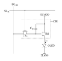
도 2는 본 발명의 일 실시예에 따른 표시 장치의 화소 회로를 나타낸 회로도이다. 특히, 도 2에 도시된 화소 회로는 유기발광 표시 장치의 화소 회로를 나타낸다. 설명의 편의를 위하여, 제 m 데이터 라인(DLm) 및 제 n 스캔 라인(SLn)에 접속된 화소 회로가 도시되었다.2 is a circuit diagram showing a pixel circuit of a display device according to an embodiment of the present invention. Particularly, the pixel circuit shown in Fig. 2 represents a pixel circuit of the organic light emitting diode display. For convenience of explanation, pixel circuits connected to the m-th data line DLm and the n-th scan line SLn are shown.
도 2를 참조하면, 화소(PX)는 유기발광다이오드(OLED; Organic light emitting diode) 및 유기발광다이오드(OLED)에 전류를 공급하는 화소회로(CIR)를 포함할 수 있다. 한편, 화소회로(CIR)는 복수의 트랜지스터(TR1, TR2) 및 커패시터(Cst) 을 포함할 수 있다. 복수의 트랜지스터(TR1 및 TR2)은 박막 트랜지스터(Thin film transistor: TFT)일 수 있다. 도 2에서, 화소회로(CIR)는 두 개의 트랜지스터(TR1, TR2) 및 하나의 커패시터(Cst)를 포함하는 것으로 도시되었으나, 이에 제한되는 것은 아니다. 화소회로(CIR)는 데이터 신호에 대응하는 전류를 유기발광 다이오드(OLED)로 공급할 수 있도록 다양한 형태로 구성될 수 있다.Referring to FIG. 2, the pixel PX may include an organic light emitting diode (OLED) and a pixel circuit (CIR) that supplies a current to the organic light emitting diode OLED. On the other hand, the pixel circuit (CIR) may include a plurality of transistors (TR1, TR2) and a capacitor (Cst). The plurality of transistors TR1 and TR2 may be a thin film transistor (TFT). In Fig. 2, the pixel circuit (CIR) is shown as including two transistors (TR1, TR2) and one capacitor (Cst), but is not limited thereto. The pixel circuit (CIR) may be configured in various forms to supply a current corresponding to the data signal to the organic light emitting diode (OLED).
유기발광다이오드(OLED)의 애노드 전극은 화소회로(CIR)에 접속되고, 캐소드 전극은 접지 전압(ELVSS)을 공급하는 접지 전원에 접속된다. 이와 같은 유기발광 다이오드(OLED)는 화소회로(CIR)로부터 공급되는 전류에 대응하여 광을 생성한다.The anode electrode of the organic light emitting diode (OLED) is connected to the pixel circuit (CIR), and the cathode electrode is connected to the ground power supply for supplying the ground voltage (ELVSS). The organic light emitting diode OLED generates light corresponding to the current supplied from the pixel circuit CIR.
화소회로(CIR)는 스캔 라인(SLn)으로 스캔 신호가 공급될 때, 데이터 라인(DLm)으로부터 데이터 신호를 공급받는다. 스캔 라인(SLn)을 통해 스캔 신호가 인가되면, 제1 트랜지스터(TR1)가 턴온되고, 데이터 라인(DLm)을 통해 제공되는 데이터 신호가 제2 트랜지스터(TR2)의 게이트 단자로 인가된다. 이때, 데이터 신호는, 제2 트랜지스터(TR2)의 턴온/턴오프를 제어하는 신호이다. 인가되는 데이터 신호에 응답하여, 제2 트랜지스터(TR2)가 턴온되면 구동 전원(ELVDD)이 유기발광다이오드(OLED)의 애노드 전극에 인가되어, 유기발광다이오드(OLED)를 통해 전류(I)가 흐르게 된다. 이에 따라, 유기발광다이오드(OLED)가 발광하게 된다. 이때, 전류(I) 값은 유기발광 다이오드(OLED)의 양단에 인가되는 전압, 즉 구동 전원(ELVDD) 및 접지 전원(ELVSS)의 전압값에 따라 달라지게 된다. 제2 트랜지스터(TR2)가 턴오프되면, 유기발광다이오드(OLED)이 애노드 전극이 플로팅되어, 유기발광다이오드(OLED)가 소광하게 된다. 한편, 커패시터(Cst)는 구동 전원(ELVDD)과 인가된 데이터 신호의 전압 차이에 대응한 전압을 저장함으로써, 제1 트랜지스터(TR1)가 턴오프되어 데이터 신호가 인가되지 않을 때도, 제2 트랜지스터(TR2)가 턴온 또는 턴오프 상태를 유지할 수 있도록 한다.The pixel circuit CIR receives a data signal from the data line DLm when a scan signal is supplied to the scan line SLn. When the scan signal is applied through the scan line SLn, the first transistor TR1 is turned on and the data signal supplied through the data line DLm is applied to the gate terminal of the second transistor TR2. At this time, the data signal is a signal for controlling the turn-on / turn-off of the second transistor TR2. In response to the applied data signal, when the second transistor TR2 is turned on, the driving power source ELVDD is applied to the anode electrode of the organic light emitting diode OLED so that the current I flows through the organic light emitting diode OLED do. Thus, the organic light emitting diode OLED emits light. At this time, the value of the current I depends on the voltages applied to both ends of the organic light emitting diode OLED, that is, the voltage values of the driving power ELVDD and the ground power ELVSS. When the second transistor TR2 is turned off, the anode electrode of the organic light emitting diode OLED floats, and the organic light emitting diode OLED is extinguished. The capacitor Cst stores a voltage corresponding to the voltage difference between the driving power ELVDD and the applied data signal so that even when the first transistor TR1 is turned off and the data signal is not applied, TR2 can be kept on or off.
도 3은 종래의 유기 발광 표시 장치의 디지털 구동의 개념도이다.3 is a conceptual diagram of digital driving of a conventional organic light emitting diode display.
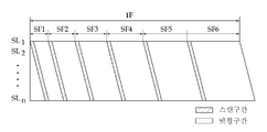
디지털 구동은 제2 트랜지스터의 게이트에 온 또는 오프 2가지의 조건의 전압만을 인가한다. 화소가 출력하는 발광량의 정도에 따라 계조를 표현할 수는 없지만, 서브필드의 조합으로 화소(PX)의 발광 시간을 조정하는 방식으로 계조를 구현한다.The digital driving applies only two voltages to the gate of the second transistor on or off. The gradation can not be expressed according to the degree of the amount of light emitted by the pixel, but the gradation is implemented by a method of adjusting the light emission time of the pixel PX by the combination of the subfields.
서브필드란 영상 기준시간 프레임을 복수의 서로 다른 발광 시간 가중치의 시간 단위로 분할한 개념이다. 서로 다른 발광시간을 가진 서브필드의 선택 조합을 통해서 계조를 구현할 수 있다. 서브필드를 이용하여 발광구간의 시간 길이 조절로 계조를 표현하는 방식은 2진수를 이용하여 숫자를 표기하는 방법을 이용하여 설명하는 것이 가능하다. 가중치 설정은 예를 들어, 1 프레임을 6개의 서브필드로 나누어 구성하고 각 서브필드마다 이전 서브필드에 비해서 2배의 발광 시간을 할당하도록 구성한다고 가정해 본다. 6개의 서브필드는 각 자릿수 마다 2진수의 자릿수에 해당하는 가중치로서 휘도를 표시할 수 있다. 제1 서브필드(SF1)의 가중치를 20으로 설정하고, 제2 서브필드(SF2)의 가중치를 21로 설정하는 식으로, 가중치가 2n(n=0,1,2,3,4,5)의 비율로 증가되도록 각 서브필드의 가중치를 결정할 수 있다.The sub-field is a concept in which an image reference time frame is divided into time units of a plurality of different light emission time weight values. The gradation can be realized through the selective combination of the subfields having different emission times. A method of expressing a gray level by adjusting the time length of a light emitting section using a subfield can be described using a method of expressing a number using binary numbers. For example, it is assumed that one frame is divided into six subfields, and the weighting is configured to allocate twice the light emission time to the previous subfields for each subfield. The six subfields can display the luminance as a weight value corresponding to the number of digits of the binary number for each digit. The first sub-field (SF1) the weights of the weight set to 20, and the second subfield (SF2) in such a manner as to set to 21, the weight is 2 n (n = 0,1,2,3,4 , ≪ / RTI > 5).
따라서, 표시 장치는 온-오프 조합을 통해서 서브필드 데이터로 26 = 64가지의 휘도 계조를 표현하는 것이 가능하다. 서브필드의 배열 순서를 발광구간의 시간 길이가 긴 즉 휘도 가중치가 높은 서브필드부터 내림차순으로 하면 SF6, SF5, SF4, SF3, SF2, SF1의 순서가 된다.Therefore, the display apparatus can express 2 6 = 64 luminance gradations in the subfield data through on-off combination. SF6, SF5, SF4, SF3, SF2, and SF1 are arranged in descending order from the sub field having the longest time length of the light emission period, that is, the subfield having the highest luminance weight.
각 서브필드의 데이터 전압값이 온 상태(예를 들어, 5V)를 이진수의 '1'로 나타내고 각 서브필드의 데이터 전압값이 오프 상태(예를 들어, 0V)를 이진수의 '0'으로 나타내면, 화소의 계조를 나타낼 수 있다. 예를 들어, 63 계조는 이진수의 '11 1111'로 표현되므로, 하나의 프레임 내에 각 서브필드가 모두 온 상태, 즉 "SF6, SF5, SF4, SF3, SF2, SF1" = "On, On, On, On, On, On"로 63 계조가 표현될 수 있다. 이는 해당 화소가 프레임 내의 모든 서브필드에서 온 데이터를 입력 받아서 발광하는 상태임을 의미한다. 또한, 계조 6는 "00 0110"으로 표현될 수 있고, 하나의 프레임 내에 서브필드 1과 서브필드 3이 온 상태, 즉 "SF6, SF5, SF4, SF3, SF2, SF1" = "Off, Off, Off, On, On Off"로 화소가 서브필드 2와 서브필드 3에서만 발광하여 6 계조를 표현할 수 있다. 이와 같이, 한 프레임 기간 동안 화소들(PX)의 발광 시간을 조절하여 계조가 표현될 수 있다.If the data voltage value of each subfield is represented by '1' of binary number in an ON state (for example, 5V) and the data voltage value of each subfield is represented by an OFF state (for example, 0V) , And the gradation of the pixel can be expressed. For example, since the 63 gradations are represented by '111111' of binary numbers, all the subfields are turned on in one frame, that is, "SF6, SF5, SF4, SF3, SF2, SF1" , On, On, On ". This means that the corresponding pixel is in a state of emitting data by receiving data from all the subfields in the frame. SF6, SF4, SF3, SF2, SF1 = "Off, Off, Off " Off, On, On Off ", the pixel can emit light only in the
도 4는 본 발명의 일 실시예에 따른 입체 영상의 표시 구성도이다.4 is a block diagram of a stereoscopic image according to an exemplary embodiment of the present invention.
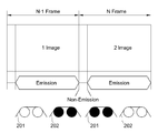
도 4에서 X축은 시간축을 나타내고 Y측은 표시부의 수직 위치(vertical position)을 나타낸다. 3D 입체 영상을 구현하기 위해서는 표시부(110)에서 프레임(Frame)마다 좌안 영상데이터와 우안 영상데이터를 교번하여 출력하여야 한다. 또한 셔터 안경(200)은 프레임 주기와 동일하게 동기화되어 좌우안 셔터를 개폐한다.In Fig. 4, the X-axis represents the time axis and the Y-axis represents the vertical position of the display portion. In order to realize a 3D stereoscopic image, the
본 발명의 실시예에 따른 표시 패널은 좌안 표시 구간(N-1 Frame)에 좌안 영상데이터(Left Image)를 표시한다. 표시패널과 동기된 셔터 안경(200)은 좌안 셔터를 열고, 우안 셔터를 닫는다. 즉, 좌안 셔터는 광이 통과할 수 있도록 광투과율을 높이고, 우안 셔터는 광이 통과할 수 없도록 광투과율을 낮추는 것이다. 이를 통해 셔터 안경을 사용하는 사용자는 좌안 표시 구간(N-1 Frame) 동안 열려있는 좌안 셔터를 통해서 좌안 영상을 볼 수 있다.The display panel according to the embodiment of the present invention displays left eye image data (Left Image) in a left eye display period (N-1 Frame). The
좌안 표시 구간(N-1 Frame)에 이어 우안 표시 구간(N Frame)에서 표시패널은 우안의 영상데이터(Right Image)를 표시한다. 이때 셔터 안경(200)은 우안 셔터를 열고, 좌안 셔터를 닫는다. 사용자는 우안 표시 구간(N Frame)동안 열려있는 우안 셔터를 통해서 우안 영상을 볼 수 있다.In the right eye display section (N Frame) following the left eye display section (N-1 Frame), the display panel displays right eye image data (Right Image). At this time, the
프레임(Frame)의 발광 구간 사이에 비발광(Non-Emission)구간이 위치한다. 비발광(Non-Emission)구간에서 표시 장치는 비발광 상태이다. 구동전압(ELVDD) 또는 접지전압(ELVSS)의 전압을 조정하여 전원부(150)가 구동전압과 접지전압의 차이를 0으로 유지하면, 전체 화소는 발광하지 않는다.A non-emission period is located between the emission periods of the frame. In the non-emission period, the display device is in a non-emission state. When the
비발광(Non-Emission)구간에서 스캔 라인과 데이터 라인을 통해서 발광 정보가 화소에 전달되어, 각 화소의 스토리지 커패시터(Cst)에 저장된다.In the non-emission period, the light emission information is transmitted to the pixel through the scan line and the data line, and is stored in the storage capacitor Cst of each pixel.
도 5는 본 발명의 일 실시예에 따른 듀얼 영상의 표시 구성도이다.FIG. 5 is a diagram illustrating a display configuration of a dual image according to an exemplary embodiment of the present invention. Referring to FIG.
도 5를 참조하면, 듀얼 2D 영상을 구현하기 위하여 표시부(110)는 프레임(Frame)마다 제1 영상과 제2 영상을 교번하여 출력하여야 한다. 제1 영상(1 Image)과 제2 영상(2 Image)은 서로 다른 정보를 표시하는 영상으로서, 예를 들면 다른 방송 채널을 통해서 입력 받은 영상 정보이다.Referring to FIG. 5, in order to implement a dual 2D image, the
듀얼 2D 표시 방식은 서로 다른 시청자에게 하나의 표시 장치를 통해서 서로 다른 영상 정보를 제공하기 위한 구동 방법이다. 서로 다른 사용자는 각각 동기화된 주기가 다른 복수의 셔터 안경(201, 202)를 사용한다.The dual 2D display method is a driving method for providing different image information to different viewers through one display device. Different users use a plurality of
표시 패널은 제1 영상 표시 구간(N-1 Frame)에 제1 영상(1 Image)을 표시한다. 제1 영상이 표시되는 동안, 제1 영상에 동기된 제1 셔터안경(201)은 양안의 셔터를 모두 연 상태로 있다. 반대로 제2 영상용 제2 셔터 안경(202)은 양안의 셔터를 모두 닫고 있다.The display panel displays the first image (1 Image) in the first image display period (N-1 Frame). While the first image is being displayed, the
제2 영상 데이터 표시 구간(N Frame)에 표시패널이 제2 영상 데이터(2 Image)를 표시한다. 이때 제2 영상에 동기된 제2 셔터안경(202)은 양안의 셔터를 모두 연 상태인 반면, 제1 셔터안경(201)은 양안의 셔터를 모두 닫은 상태이다. And the display panel displays the second image data (2 Image) in the second image data display period (N Frame). At this time, the
즉, 제1 셔터안경을 사용한 사용자는 제1 영상 만을 보고, 제2 셔터안경을 사용한 사용자는 제2 영상 만을 볼 수 있으므로, 하나의 표시패널이 서로 다른 2개의 영상 정보를 제공할 수 있게 된다.That is, a user using the first shutter glasses can view only the first image, and a user using the second shutter glasses can view only the second image, so that one display panel can provide two different image information.
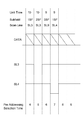
도 6은 본 발명의 일 실시예에 따른 프레임의 타이밍도이다. 6 is a timing diagram of a frame according to an embodiment of the present invention.
본 발명의 실시예에서 설명의 편의성을 위하여 표시패널(110)이 10개의 스캔 라인 (SL1 내지 SL10)만을 포함하고 있다고 가정하기로 한다.For convenience of description, it is assumed that the
도 6의 X 축은 시간 축이고 Y 축은 스캔 라인(SL)을 의미한다.The X-axis in Fig. 6 denotes a time axis and the Y-axis denotes a scan line SL.
도 6을 참조하면, 동시구동 방식은 프레임을 시간적으로 연속된 각각의 단위시간(Unit time)으로 나누고, 각 단위시간 내에서 서로 다른 스캔 라인의 화소에 각 프레임에 할당된 서브필드의 데이터 정보를 기입한다.Referring to FIG. 6, in the simultaneous driving method, a frame is divided into a plurality of unit time periods consecutively in time, and data information of subfields allocated to each frame to pixels of different scan lines within each unit time .
도 6은 서브필드의 가중치가 높은 순서대로 서브필드 0 부터 5까지 총 6개의 서브필드가 사용되는 것을 예시하고 있다.FIG. 6 illustrates that a total of six subfields are used from the
단위시간(Unit time)은 영상 프레임(N Frame)을 구성하는 구동 시간을 나타내는 개념이다. 프레임은 비발광구간(Non-Emission)과 발광구간(Emission)으로 나누어지고, 발광구간에서 단위시간 개수는 표시패널(110)의 스캔 라인수(SLn)와 동일할 수 있다.The unit time is a concept representing a driving time of an image frame (N frame). The frame may be divided into a non-emission period and an emission period, and the number of unit times in the light emission period may be equal to the number of scan lines SLn of the
또한, 각 단위시간은 서브필드와 동일한 개수의 선택시간으로 나누어질 수 있다.In addition, each unit time can be divided into the same number of selection times as the subfields.
선택시간(Selection time)은 어느 하나의 스캔 라인으로 스캔신호를 인가하거나 또는 각 화소에 데이터 신호를 공급할 수 있는 최소의 시간이다. 각 선택시간(Selection time)에 한 스캔 라인에 인가되는 스캔신호와 각 화소에 데이터 전압이 인가된다. 각 화소에 인가되는 데이터 정보는 각 서브필드별 온-오프에 대응하는 정보이며, 도 6에 스캔 라인과 선택시간의 교차 지점에 인가되는 데이터의 해당 서브필드가 숫자로 표기되어 있다.The selection time is a minimum time for applying a scan signal to one scan line or supplying a data signal to each pixel. At each selection time, a scan signal applied to one scan line and a data voltage are applied to each pixel. The data information applied to each pixel is information corresponding to ON / OFF of each subfield. In FIG. 6, the corresponding subfield of the data applied at the intersection of the scan line and the selection time is indicated by a number.
스캔 라인에 인가된 스캔 신호에 의하여 각 서브필드가 시작되기 전에 스캔라인의 화소들은 기존에 기입된 서브필드에 의해서 발광 또는 비발광 상태를 유지한다.The pixels of the scan line maintain a light emitting state or a non-light emitting state by the previously written subfields before the start of each subfield by the scan signal applied to the scan line.
본 발명의 실시예에서 발광구간은 패널의 스캔 라인수와 동일한 10개의 단위시간으로 나누어지며, 각 단위시간은 다시 서브필드수와 동일한 6개의 선택시간으로 분할된다. 따라서, 발광구간 내에는 총 60개의 선택시간이 존재한다.In the embodiment of the present invention, the light emitting period is divided into 10 unit time, which is the same as the number of scan lines of the panel, and each unit time is divided into six selection times equal to the number of the subfields. Therefore, there are a total of 60 selection times in the light emission section.
서브필드의 가중치는 서브필드가 시작된 선택시간부터 다음 서브필드가 시작되기 전까지이며, 각 서브필드의 가중치는 선택시간의 합과 동일하다.The weight of the subfield is from the selected time from the start of the subfield to the start of the next subfield, and the weight of each subfield is equal to the sum of the selected times.
예를 들어, 발광시간이 60개의 선택시간으로 구성되면, 제0 내지 제6 서브필드의 가중치도 60이 된다. 따라서, 제0 서브필드 내지 제5 서브필드에 "31", "13", "8", "5", "2", "1"의 가중치에 대응되는 개수만큼 선택 시간이 분배되어 각 서브필드가 설정될 수 있다.For example, if the light emission time is composed of 60 selection times, the weights of the 0th to 6th subfields are 60. [ Therefore, the selection time is distributed to the 0th subfield to the 5th subfield by the number corresponding to the weight of "31", "13", "8", "5", "2" Can be set.
본 발명의 실시예와 같이 서브필드를 단위시간 기준으로 구성하면, 제1 스캔 라인을 제외한 다른 스캔 라인의 제0 서브필드는 제2 내지 제10 단위시간 중 어느 하나에 위치할 수 있다. 전 스캔 라인이 동일한 서브필드 가중치를 갖기 위하여, 제 1 스캔라인을 제외한 다른 스캔 라인은 제0 서브필드 이전에 존재하는 발광구간의 선택시간에도 다른 서브필드를 할당하여야 한다.If the subfields are formed on a unit time basis as in the embodiment of the present invention, the 0th subfield of the other scan lines except for the first scan line may be positioned in any one of the second to tenth unit time periods. Other scan lines other than the first scan line must allocate different subfields to the selection time of the light emission period existing before the 0th subfield so that all scan lines have the same subfield weights.
도 6을 참조하면, 비발광구간(Non-Emission)에 서브필드 온-오프 정보를 가지는 프리-데이터(Pre-data)가 화소에 기입된다. 프리-데이터 기입을 통해서 모든 스캔 라인의 화소가 발광구간의 시작점부터 서브필드 온-오프 정보에 따라 발광 또는 비발광할 수 있게 된다. Referring to FIG. 6, pre-data having sub-field on-off information in a non-emission period is written to a pixel. The pixels of all the scan lines can emit light or not emit light according to the subfield on-off information from the start point of the light emitting period through the pre-data write.
프리-데이터가 화소에 기입되므로서 하나의 프레임에서 해당 서브필드의 가중치를 만족하도록 발광구간의 시작점부터 가중치의 일부를 할당할 수 있게된다.예를 들어, 제2 스캔 라인(SL2)의 화소가 모든 서브필드에서 발광한다고 가정하고, 발광구간에서 제0 서브필드의 시작점(제2 단위시간 - 제1 선택시간)부터 동작을 살펴본다.Since the pre-data is written in the pixel, a part of the weight can be allocated from the start point of the light emitting period so as to satisfy the weight of the corresponding sub-field in one frame. It is assumed that all subfields emit light, and the operation will be examined from the starting point (second unit time - first selection time) of the 0th subfield in the light emitting period.
제2 스캔 라인(SL2)의 화소는 제0 내지 제2 서브필드 구간에서 데이터 전압을 인가받고, 제3 서브필드의 시작점(제10 단위시간 제4 선택시간)부터 제10 단위시간의 제5 선택시간까지(가중치 '2')에 해당하는 두 칸의 선택시간동안 데이터 전압을 인가받는다.The pixel of the second scan line SL2 receives the data voltage in the 0th to 2nd subfield periods and receives the data voltage from the start point of the third subfield (fourth tenth unit time period) The data voltage is applied during the selection time of two cells corresponding to the time (weight '2').
계조를 표현하기 위해서는 제2 스캔라인(SL2)의 화소는 제3 서브필드에서 '3' 가중치와 제4 서브필드에서 '2' 가중치, 제5 서브필드의 '1' 가중치에 해당하는 서브필드 데이터를 모두 인가받아야 한다. 그러나, 제2 스캔 라인(SL2)는 제3 서브필드의 시작점 이후에 제3 서브필드의 일부, 제4 서브필드 및 제5 서브필드의 가중치를 할당할 수 없다.In order to express the gradation, the pixel of the second scan line SL2 is divided into subfield data corresponding to '3' weight in the third subfield, '2' weight in the fourth subfield, and '1' . However, the second scan line SL2 can not assign the weight of the third subfield, the fourth subfield, and the fifth subfield after the start point of the third subfield.
이에 따라, 본 발명의 실시예에 따른 구동 방식은 제3 서브필드의 '3' 가중치와 제4 서브필드의 '2'가중치, 제5 서브필드의 '1'가중치를 발광구간 시작점부터 제0 서브필드의 시작점까지의 구간에 할당한다.Accordingly, in the driving method according to the embodiment of the present invention, the '3' weight of the third sub-field, the '2' weight of the fourth sub-field, and the '1' weight of the fifth sub- To the start of the field.
프리-데이터 신호에 후속하는 서브필드 데이터를 발광 구간의 제0 서브필드 이전에 인가함으로써 전 프레임에 균등하게 서브필드를 할당할 수 있게 된다.The subfield data subsequent to the pre-data signal is applied before the 0th subfield of the light emitting period, so that the subfields can be evenly allocated to the previous frame.
또한, 본 발명의 실시예에 따른 구동 방식은 발광구간의 시작점에서부터 발광이 진행될 수 있도록 비발광구간에서 발광구간의 시점에 필요한 서브필드 정보를 화소에 미리 입력한다.In addition, in the driving method according to the embodiment of the present invention, the subfield information required at the time of the light emitting period in the non-light emitting period is input to the pixel in advance so that light emission can proceed from the starting point of the light emitting period.
비발광구간에서, 스캔 라인(SL1 내지 SL10)에 순차적으로 각 선택시간에 스캔 신호가 각각 인가되고, 스캔 신호와 동기하여 발광구간의 종료 시점의 서브필드와 동일한 서브필드의 데이터가 화소에 인가된다.In the non-emission period, the scan signals are sequentially applied to the scan lines SL1 to SL10 at each selection time, and the data of the subfields that are the same as the subfields at the end of the emission period are applied to the pixels in synchronization with the scan signals .
이에 따라, 비발광구간이 종료한 후 발광구간이 시작할 때, 발광구간의 종료 시점의 서브필드 데이터가 화소에 미리 인가되어, 한 프레임에서 각 스캔 라인의 화소에 서브필드의 가중치가 전부 할당될 수 있다.Accordingly, when the light emitting period starts after the non-light emitting period ends, the subfield data at the end of the light emitting period is applied to the pixels in advance, and the weight of the subfield is allotted to the pixels of each scan line in one frame have.
구체적으로, 제2 스캔 라인(SL2)의 화소에 인가되는 스캔 신호와 서브필드 데이터의 타이밍 동작을 살펴보기로 한다.More specifically, the timing operation of the scan signal and the subfield data applied to the pixels of the second scan line SL2 will be described.
제2 스캔 라인(SL2)의 화소는 비발광구간의 제2 선택시간에 스캔 신호와 발광구간의 종료 시점과 동일한 제3 서브필드 데이터를 프리-데이터 신호로 인가받는다.The pixels of the second scan line SL2 receive the scan signal and the third sub-field data equal to the end time of the emission period as a pre-data signal at the second selection time of the non-emission period.
프리-데이터 신호는 비발광구간에서 제2 스캔 라인(SL2)의 화소의 스토리지 커패시터(Cst)에 저장되고, 제2 스캔 라인(SL2)의 화소는 발광구간의 초기 시점인 제1 단위시간부터 스토리지 커패시터(Cst)에 저장된 전압에 의해 발광(또는 비발광)한다.The pre-data signal is stored in the storage capacitor Cst of the pixel of the second scan line SL2 in the non-emission period and the pixel of the second scan line SL2 is stored in the storage unit (Or non-emitted) by the voltage stored in the capacitor Cst.
또한, 제2 스캔 라인(SL2)의 화소는 발광구간에서 계속하여 제0 서브필드 이전에 제4 서브필드와 제5 서브필드 데이터를 인가받는다. The pixels of the second scan line SL2 are continuously supplied with the fourth subfield and the fifth subfield data before the 0th subfield in the light emission period.
즉, 비발광구간에 프리-데이터 기입 동작을 수행함으로써 발광구간에서 각 스캔라인의 화소에 동일한 서브필드의 가중치가 할당될 수 있어 비순차로 스캔 동작에도 불구하고 표시 패널은 원하는 화상을 표시할 수 있다.In other words, by performing the pre-data write operation in the non-emission period, the same sub-field weight can be assigned to the pixels of each scan line in the light emission period, so that the display panel can display the desired image have.
다만, 동일한 서브필드가 발광구간과 비발광구간에서 분할되어 화소에 인가되는 경우, 데이터 드라이버로부터 화소에 인가된 데이터 전압 파형이 발광구간과 비발광구간에서 동일한 서브필드임에도 불구하고 서로 다르게 되어, 표시 패널의 휘도가 불균일해질 수 있다.However, when the same sub-field is applied to the pixel in the light emitting period and the non-light emitting period, the data voltage waveform applied to the pixel from the data driver is different from each other in spite of the light emitting period and the non- The brightness of the panel may become uneven.
유기 전계 발광 표시 장치는 제2 트랜지스터에 인가되는 게이트 전압에 의해서 발광량이 결정되기 때문에 화소에 인가되는 데이터 전압의 작은 차이에 의해서도 불균일한 휘도를 나타낼 수 있다. 데이터 전압의 파형이 변경되어 표시 패널의 휘도가 불균일한 현상을 충전성 휘도 불균일이라 한다.Since the light emission amount is determined by the gate voltage applied to the second transistor, the organic light emitting display device may exhibit a non-uniform luminance even by a small difference in the data voltage applied to the pixel. The phenomenon in which the waveform of the data voltage is changed and the luminance of the display panel is uneven is referred to as chargeable luminance unevenness.
충전성 휘도 불균일은 특히 스캔 신호가 1us 이하인 고속 스캔 방식을 사용하는 대면적 유기 발광 표시 장치에서 더 많이 발생한다.Charging luminance unevenness occurs more particularly in a large area organic light emitting display using a high-speed scanning method in which a scan signal is 1us or less.
도 7은 본 발명의 다른 실시예에 따른 영상 프레임을 나타내는 구동 타이밍도이다.7 is a driving timing diagram showing an image frame according to another embodiment of the present invention.
도 8은 본 발명의 다른 실시예에 따른 영상 프레임의 비발광구간에서 데이터 신호 및 스캔 신호를 나타내는 파형도이다.8 is a waveform diagram showing a data signal and a scan signal in a non-emission period of an image frame according to another embodiment of the present invention.
도 7과 도 8를 참조하여 비발광구간(Non-Emission)에서 더미-데이터(Dummy-data) 신호를 프리-데이터(Pre-data)신호 이전에 인가하여 발광구간과 비발광구간의 데이터 파형을 실질적으로 동일하게 인가하는 방법을 설명하기로 한다.Referring to FIGS. 7 and 8, a dummy-data signal is applied before a pre-data signal in a non-emission period to generate a data waveform of a light emitting period and a non- A method of applying the same substantially the same will be described.
더미-데이터 신호는 발광구간에서 프리-데이터 신호에 대응하는 서브필드 데이터보다 바로 전의 선택 시간에서 시작된 다른 스캔 라인의 서브필드 데이터와 동일한 신호로서, 프리-데이터 신호의 전의 적어도 하나의 선택 시간에 인가된다. 이를 통해, 프리-데이터의 드라이버 인가 조건을 발광구간의 데이터 인가 조건과 동일하게 구현할 수 있다.The dummy-data signal is the same as the subfield data of the other scan lines started at the selection time immediately before the subfield data corresponding to the pre-data signal in the light emission period, and is applied to at least one selection time before the pre- do. Accordingly, the driver application condition of the pre-data can be implemented in the same manner as the data application condition of the light emission period.
도 7과 도 8를 참조하여, 제3 스캔 라인(SL3)과 제4 스캔 라인(SL4)의 비발광구간의 파형을 설명하기로 한다.The waveforms of the non-emission periods of the third scan line SL3 and the fourth scan line SL4 will be described with reference to FIGS. 7 and 8. FIG.
도 7에 도시된 바와 같이, 제3 스캔 라인(SL3)의 프리-데이터(제2 서브필드 데이터)는 제10 단위시간의 제2 선택시간에 입력된 제2 서브필드의 데이터와 동일한 신호이다.7, the pre-data (second sub-field data) of the third scan line SL3 is the same as the data of the second sub-field input at the second selection time of the tenth unit time.
또한, 도 8에 도시된 바와 같이, 제3 스캔 라인(SL3)의 더미-데이터(제1 서브필드 데이터)는 발광구간에서 제3 스캔 라인(SL3)의 프리-데이터 신호에 대응하는 서브필드 데이터보다 바로 전의 선택 시간에서 시작된 제5 스캔 라인(SL5)의 서브필드 데이터(제1 서브필드 데이터)와 동일한 신호로서 적어도 하나의 선택 시간 동안 인가된다.8, the dummy-data (first sub-field data) of the third scan line SL3 is the sub-field data corresponding to the pre-data signal of the third scan line SL3 in the emission period Field data (first sub-field data) of the fifth scan line SL5 started at the immediately preceding selection time, for at least one selection time.
프리-데이터 신호는 하나의 프레임에서 해당 서브필드의 가중치를 만족하도록 발광구간의 시작점에서 가중치의 일부를 할당하는 역할을 수행한다.The pre-data signal performs a function of allocating a part of the weight at the starting point of the light emitting period so as to satisfy the weight of the corresponding sub-field in one frame.
한편, 도 8에 도시된 바와 같이, 더미-데이터 신호 인가 시에 스캔 신호는 화소에 인가되지 않을 수 있다. 더미 데이터 신호는 화소에 인가되는 비발광 구간의 프리-데이터 신호 파형과 발광 구간의 종료 시점의 서브필드 데이터의 파형과 동일하게 인가하기 위한 것이기 때문이다.On the other hand, as shown in FIG. 8, when a dummy-data signal is applied, a scan signal may not be applied to the pixel. This is because the dummy data signal is for applying the waveform of the pre-data signal in the non-emission period applied to the pixel and the waveform of the sub-field data at the end of the emission period.
도 9는 이전 프레임(N-1Fram)과 현 프레임(N Frame)의 비발광구간의 연결 구간을 나타내는 타이밍도이다.9 is a timing chart showing a connection section of a non-light emission section of a previous frame (N-1 Fram) and a current frame (N Frame).
도 9를 참조하면, 이전 프레임(N-1 Frame)을 구성하는 서브필드의 배치와 현 프레임(N Frame)을 구성하는 서브필드의 배치는 동일하다. 현프레임(N Frame)의 비발광구간에 인가되는 프리-데이터 정보는 현 프레임(N Frame)에 기입될 데이터 정보에 기초하여 비발광 구간에 입력된다.Referring to FIG. 9, the arrangement of the subfields constituting the previous frame (N-1 frame) and the arrangement of the subfields constituting the current frame (N frame) are the same. The pre-data information applied in the non-emission period of the current frame (N Frame) is input to the non-emission period based on the data information to be written in the current frame (N Frame).
이전 프레임(N-1 Frame)의 발광구간에서 스캔은 비순차적으로 이루어지며, 현 프레임(N Frame)의 비발광구간에서 스캔은 순차적으로 이루어진다.In the light emitting period of the previous frame (N-1 frame), the scanning is performed in a non-sequential manner, and the scanning is sequentially performed in the non-emitting period of the current frame (N frame).
본 발명의 실시예에 따른 표시 장치는 도4와 도5에서 설명한 3D 표시 장치 또는 듀얼 2D 표시 장치에 적용될 수도 있다.The display device according to the embodiment of the present invention may be applied to the 3D display device or the dual 2D display device described in Figs. 4 and 5.
3D 표시장치 또는 듀얼 2D 표시 장치에 적용하기 위해서는 외부로부터 서로다른 제1 영상정보와 제2 영상정보의 입력을 받아야 한다.In order to apply to a 3D display device or a dual 2D display device, first and second image information different from each other must be input from the outside.
외부로부터 받은 제1 영상정보는 제1 프레임에 표시하고, 제 1영상정보와 서로 다른 제2 영상정보는 제1 프레임과 연속한 제2 프레임에 표시한다.The first image information received from the outside is displayed on the first frame, and the second image information different from the first image information is displayed on the second frame continuous with the first frame.
본 발명의 실시예를 통해 설명한 바와같이 제1 프레임은 비발광 구간과 발광구간으로 구성되며, 비발광 구간에 더미-데이터 신호와 프리-데이터 신호를 인가하는 것을 통해, 발광구간에서 제1 영상정보를 온전히 표시할 수 있다. As described in the embodiment of the present invention, the first frame is composed of a non-emission period and a light emission period. By applying the dummy-data signal and the pre-data signal to the non-emission period, Can be displayed completely.
프리-데이터 신호는 해당 프레임의 발광구간의 종료시점에서 서브필드 데이터와 동일한 데이터를 갖는다.The pre-data signal has the same data as the sub-field data at the end of the emission period of the frame.
더미-데이터는 발광구간에서 프리-데이터 신호에 대응하는 서브필드 데이터보다 바로 전의 선택 시간에서 시작된 다른 스캔 라인의 서브필드 데이터와 동일한 데이터를 갖는다. The dummy-data has the same data as the subfield data of the other scan lines started at the selection time immediately before the subfield data corresponding to the pre-data signal in the light emission period.
제2 프레임도 제1 프레임과 동일한 프레임 구성을 가진다.The second frame also has the same frame configuration as the first frame.
각 프레임의 발광구간에 동기하여 셔터안경이 동기화 방식은 되는 것은 도4 내지 도5의 설명과 동일하다.The synchronization of the shutter glasses in synchronization with the light emission period of each frame is the same as that of Figs. 4 to 5.
그러나, 본 발명의 범위가 상기 특정한 실시예로 한정되는 것은 아니며, 본 발명의 사상 및 기술 범위에 포함되는 모든 변경, 균등물 또는 대체물은 본 발명의 범위에 포함되는 것으로 이해되어야 한다.It is to be understood, however, that the scope of the present invention is not limited to the specific embodiments described above, and all changes, equivalents, or alternatives falling within the scope and spirit of the present invention are included in the scope of the present invention.
100: 표시 장치
110: 표시 패널
120: 제어부
130: 데이터 드라이버
140: 스캔 드라이버
150: 전원부
200,201,202: 셔터안경100: display device 110: display panel
120: control unit 130: data driver
140: scan driver 150:
200, 201, 202: Shutter glasses
Claims (20)
복수의 스캔 라인 및
상기 데이터 라인과 상기 스캔 라인이 교차되는 지점에 위치하는 복수의 화소를 포함하는 유기발광 표시패널의 구동방법에 있어서,
비발광구간에서 각 스캔 라인의 화소에 더미-데이터 신호 및 프리-데이터 신호를 인가하는 단계;
발광구간에서 각 스캔 라인의 화소에 스캔 신호 및 데이터 신호를 비순차적으로 인가하는 단계;를 포함하되,
상기 데이터 라인에 연속되어 인가되는 상기 데이터 신호들은 서로 다른 서브필드에 대응하는 데이터 정보를 갖는 유기발광 표시패널의 구동방법.A plurality of data lines,
A plurality of scan lines and /
And a plurality of pixels positioned at intersections of the data lines and the scan lines, the method comprising:
Applying a dummy-data signal and a pre-data signal to pixels of each scan line in a non-emission period;
Sequentially applying a scan signal and a data signal to pixels of each scan line in a light emission period,
And the data signals sequentially applied to the data lines have data information corresponding to different sub-fields.
상기 데이터 신호는 복수의 서브필드 데이터를 포함하는 유기발광 표시패널의 구동방법.The method according to claim 1,
Wherein the data signal includes a plurality of sub-field data.
상기 프리-데이터 신호는 발광 구간의 종료시점에서 서브필드 데이터와 동일한 유기발광 표시패널의 구동방법.3. The method of claim 2,
Wherein the pre-data signal is the same as the sub-field data at the end of the light emitting period.
상기 프리-데이터 신호는 하나의 프레임에서 해당 서브필드의 가중치를 만족하도록 발광구간의 시작점에서 가중치의 일부를 할당하는 유기발광 표시패널의 구동방법.The method of claim 3,
Wherein the pre-data signal assigns a part of a weight at a starting point of the light emitting period so as to satisfy a weight of the corresponding sub-field in one frame.
상기 프리-데이터 신호에 후속하는 서브필드 데이터가 발광 구간에서 프레임 시작 서브필드 전에 각 스캔라인의 화소에 인가되는 유기발광 표시패널의 구동방법.5. The method of claim 4,
Wherein the subfield data following the pre-data signal is applied to the pixels of each scan line before the frame start subfield in the light emitting period.
상기 더미-데이터 신호는 발광구간에서 상기 프리-데이터 신호에 대응하는 서브필드 데이터보다 바로 전의 선택 시간에서 시작된 다른 스캔 라인의 서브필드 데이터와 동일한 유기발광 표시패널의 구동방법.The method according to claim 1,
Wherein the dummy-data signal is the same as the sub-field data of the other scan lines started at a selection time immediately before the sub-field data corresponding to the pre-data signal in the emission period.
상기 더미-데이터 신호는 상기 프리-데이터 신호의 적어도 하나의 선택 시간 전에 인가되는 유기발광 표시패널의 구동방법.The method according to claim 6,
Wherein the dummy-data signal is applied at least one selection time of the pre-data signal.
상기 스캔 신호는 상기 더미-데이터 신호가 인가될 때, 상기 스캔 라인의 화소에 인가되지 않는 유기발광 표시패널의 구동방법.The method according to claim 1,
Wherein the scan signal is not applied to the pixels of the scan line when the dummy-data signal is applied.
상기 비발광구간의 스캔 신호는 순차적으로 인가되는 유기발광 표시패널의 구동방법.9. The method of claim 8,
And the scan signals of the non-emission period are sequentially applied.
상기 스캔 신호는 상기 프리-데이터가 인가될 때, 상기 스캔 라인의 화소에 인가되는 유기발광 표시패널의 구동방법.The method according to claim 1,
Wherein the scan signal is applied to a pixel of the scan line when the pre-data is applied.
복수의 스캔 라인 및
상기 데이터 라인과 상기 스캔 라인이 교차되는 지점에 위치하는 복수의 화소를 포함하는 유기발광 표시패널의 구동방법에 있어서,
외부로부터 제1 영상정보를 입력받는 단계;
외부로부터 상기 제1영상정보와는 다른 제2 영상정보를 입력받는 단계;
제1 비발광구간에서 각 스캔 라인의 화소에 상기 제 1 영상정보에 기초한 제1 더미-데이터 신호 및 제1 프리-데이터 신호를 인가하는 단계;
제1 발광구간에서 각 스캔 라인의 화소에 제1 스캔 신호 및 상기 제 1 영상정보에 기초한 제1 데이터 신호를 비순차적으로 인가하는 단계;
제2 비발광구간에서 각 스캔 라인의 화소에 상기 제 2 영상정보에 기초한 제2 더미-데이터 신호 및 제2 프리-데이터 신호를 인가하는 단계;
제2 발광구간에서 각 스캔 라인의 화소에제2 스캔 신호 및 상기 제 2 영상정보에 기초한 제2 데이터 신호를 비순차적으로 인가하는 단계;를 포함하되,
상기 데이터 라인에 연속되어 인가되는 상기 데이터 신호들은 서로 다른 서브필드에 대응하는 데이터 정보를 갖는 유기발광 표시패널의 구동방법.A plurality of data lines,
A plurality of scan lines and /
And a plurality of pixels positioned at intersections of the data lines and the scan lines, the method comprising:
Receiving first image information from outside;
Receiving second image information different from the first image information from outside;
Applying a first dummy-data signal and a first pre-data signal based on the first image information to pixels of each scan line in a first non-emission period;
Sequentially applying a first scan signal and a first data signal based on the first image information to pixels of each scan line in a first emission period;
Applying a second dummy-data signal and a second pre-data signal based on the second image information to pixels of each scan line in a second non-emission period;
Sequentially applying a second scan signal and a second data signal based on the second image information to pixels of each scan line in a second emission period,
And the data signals sequentially applied to the data lines have data information corresponding to different sub-fields.
상기 제1 영상 정보는 입체 영상의 좌안용 영상정보이고, 상기 제2 영상 정보는 입체 영상의 우안용 영상정보인 유기발광 표시패널의 구동방법.The method of claim 11, wherein
Wherein the first image information is the left eye image information of the stereoscopic image and the second image information is the right eye image information of the stereoscopic image.
상기 제1 및 제2 데이터 신호는 복수의 서브필드 데이터를 포함하는 유기발광 표시패널의 구동방법.12. The method of claim 11,
Wherein the first and second data signals include a plurality of sub-field data.
상기 제1 및 제2 프리-데이터 신호는 상기 제1 및 제2 발광 구간의 종료시점에서 서브필드 데이터와 동일한 유기발광 표시패널의 구동방법.14. The method of claim 13,
Wherein the first and second pre-data signals are the same as the sub-field data at the end of the first and second light emitting periods.
상기 제1 및 제2 프리-데이터 신호는 하나의 프레임에서 해당 서브필드의 가중치를 만족하도록 상기 제1 및 제2 발광구간의 시작점에서 가중치의 일부를 할당하는 유기발광 표시패널의 구동방법.15. The method of claim 14,
Wherein the first and second pre-data signals are allocated a portion of a weight at a starting point of the first and second light emitting sections so that a weight of the corresponding sub-field is satisfied in one frame.
상기 제1 및 제2 프리-데이터 신호에 후속하는 서브필드 데이터가 발광 구간에서 프레임의 최초 서브필드 전에 각 스캔 라인의 화소에 인가되는 유기발광 표시패널의 구동방법.16. The method of claim 15,
Wherein the subfield data following the first and second pre-data signals are applied to pixels of each scan line before a first subfield of a frame in a light emitting period.
상기 제1 및 제2 더미-데이터 신호는 상기 제1 및 제2 발광구간에서 상기 제1 및 제2 프리-데이터 신호에 대응하는 서브필드 데이터보다 바로 전의 선택 시간에서 시작된 다른 스캔 라인의 서브필드 데이터와 동일한 유기발광 표시패널의 구동방법.13. The method of claim 12,
The first and second dummy-data signals may include subfield data of the other scan lines starting at a selection time immediately before the subfield data corresponding to the first and second pre-data signals in the first and second emission periods And a driving method of the organic light emitting display panel.
상기 제1 및 제2 더미-데이터 신호는 상기 제1및 제2 프리-데이터 신호의 전의 적어도 하나의 선택 시간에 인가되는 유기발광 표시패널의 구동방법.18. The method of claim 17,
Wherein the first and second dummy-data signals are applied at least one selection time before the first and second pre-data signals.
상기 제1 및 제2 비발광구간의 상기 제1 및 제2 스캔 신호는 순차적으로 인가되는 유기발광 표시패널의 구동방법.19. The method of claim 18,
And the first and second scan signals in the first and second non-emission periods are sequentially applied.
상기 제1 및 제2 스캔 신호는 상기 제1 및 제2 더미-데이터 신호가 인가될 때, 상기 스캔 라인의 화소에 인가되지 않는 유기발광 표시패널의 구동방법.18. The method of claim 17,
Wherein the first and second scan signals are not applied to the pixels of the scan line when the first and second dummy-data signals are applied.
Priority Applications (2)
| Application Number | Priority Date | Filing Date | Title |
|---|---|---|---|
| KR1020140031736A KR20150108994A (en) | 2014-03-18 | 2014-03-18 | Display device and method for driving the same |
| US14/592,811 US9607535B2 (en) | 2014-03-18 | 2015-01-08 | Display device and method for driving the same |
Applications Claiming Priority (1)
| Application Number | Priority Date | Filing Date | Title |
|---|---|---|---|
| KR1020140031736A KR20150108994A (en) | 2014-03-18 | 2014-03-18 | Display device and method for driving the same |
Publications (1)
| Publication Number | Publication Date |
|---|---|
| KR20150108994A true KR20150108994A (en) | 2015-10-01 |
Family
ID=54142690
Family Applications (1)
| Application Number | Title | Priority Date | Filing Date |
|---|---|---|---|
| KR1020140031736A Withdrawn KR20150108994A (en) | 2014-03-18 | 2014-03-18 | Display device and method for driving the same |
Country Status (2)
| Country | Link |
|---|---|
| US (1) | US9607535B2 (en) |
| KR (1) | KR20150108994A (en) |
Cited By (3)
| Publication number | Priority date | Publication date | Assignee | Title |
|---|---|---|---|---|
| KR20170124790A (en) * | 2016-05-03 | 2017-11-13 | 엘지디스플레이 주식회사 | Device for digital driving based on subframe and display device comprising thereof |
| KR20180081320A (en) * | 2017-01-06 | 2018-07-16 | 삼성전자주식회사 | Electronic device and method to control display unit for sensing a biometric sensor |
| US10255839B2 (en) | 2014-10-28 | 2019-04-09 | Samsung Display Co., Ltd. | Driving unit, display device and method of driving a display panel |
Families Citing this family (2)
| Publication number | Priority date | Publication date | Assignee | Title |
|---|---|---|---|---|
| KR102395792B1 (en) | 2017-10-18 | 2022-05-11 | 삼성디스플레이 주식회사 | Display device and driving method thereof |
| KR102365146B1 (en) * | 2021-02-13 | 2022-02-23 | 이성호 | To improve sensitivity by using a modified shielding capacity of parasitic capacity |
Family Cites Families (23)
| Publication number | Priority date | Publication date | Assignee | Title |
|---|---|---|---|---|
| JPH06282242A (en) * | 1993-03-25 | 1994-10-07 | Pioneer Electron Corp | Drive device for gas discharge panel |
| EP1022714A3 (en) * | 1999-01-18 | 2001-05-09 | Pioneer Corporation | Method for driving a plasma display panel |
| JP2003186437A (en) * | 2001-12-18 | 2003-07-04 | Sanyo Electric Co Ltd | Display device |
| JP4030863B2 (en) | 2002-04-09 | 2008-01-09 | シャープ株式会社 | ELECTRO-OPTICAL DEVICE, DISPLAY DEVICE USING THE SAME, ITS DRIVING METHOD, AND WEIGHT SETTING METHOD |
| JP4357413B2 (en) * | 2002-04-26 | 2009-11-04 | 東芝モバイルディスプレイ株式会社 | EL display device |
| CA2496353C (en) * | 2002-08-20 | 2011-10-18 | Kazunari Era | Method and apparatus for generating a stereographic image |
| KR100598741B1 (en) * | 2003-12-11 | 2006-07-10 | 엘지.필립스 엘시디 주식회사 | Liquid crystal display device |
| JP4759925B2 (en) * | 2004-03-19 | 2011-08-31 | セイコーエプソン株式会社 | Electro-optical device and electronic apparatus |
| KR100805587B1 (en) * | 2006-02-09 | 2008-02-20 | 삼성에스디아이 주식회사 | Digital-to-analog converter and data drive circuit and flat panel display device using the same |
| KR100776488B1 (en) * | 2006-02-09 | 2007-11-16 | 삼성에스디아이 주식회사 | Data drive circuit and flat panel display device having the same |
| KR100952837B1 (en) * | 2008-07-28 | 2010-04-15 | 삼성모바일디스플레이주식회사 | Organic light emitting display |
| WO2010061687A1 (en) * | 2008-11-26 | 2010-06-03 | シャープ株式会社 | Liquid crystal display device, liquid crystal display device drive method, and television receiver |
| TWI386742B (en) * | 2009-04-14 | 2013-02-21 | Au Optronics Corp | Liquid crystal display and method for driving liquid crystal display panel thereof |
| JP5246433B2 (en) * | 2009-09-18 | 2013-07-24 | ソニー株式会社 | Display device |
| KR101778779B1 (en) | 2010-07-27 | 2017-09-15 | 엘지디스플레이 주식회사 | 3d image display device and driving method thereof |
| KR101279661B1 (en) | 2010-11-05 | 2013-07-05 | 엘지디스플레이 주식회사 | Stereoscopic image display and power control method thereof |
| KR20120062499A (en) * | 2010-12-06 | 2012-06-14 | 삼성모바일디스플레이주식회사 | Pixel, stereopsis display device and driving method thereof |
| JP5652188B2 (en) * | 2010-12-15 | 2015-01-14 | ソニー株式会社 | Display device |
| KR20120079609A (en) * | 2011-01-05 | 2012-07-13 | 삼성모바일디스플레이주식회사 | Scan driver and flat panel display device using the same |
| KR20120133432A (en) | 2011-05-31 | 2012-12-11 | 삼성디스플레이 주식회사 | Organic Light Emitting Display Device and Driving Method Thereof |
| CN105741780B (en) * | 2011-12-09 | 2018-12-18 | 株式会社日本有机雷特显示器 | Display unit and its driving method and electronic device |
| US9460660B2 (en) * | 2011-12-21 | 2016-10-04 | Sharp Kabushiki Kaisha | Pixel circuit and display device |
| KR101922686B1 (en) * | 2012-08-29 | 2018-11-28 | 삼성디스플레이 주식회사 | Display device |
-
2014
- 2014-03-18 KR KR1020140031736A patent/KR20150108994A/en not_active Withdrawn
-
2015
- 2015-01-08 US US14/592,811 patent/US9607535B2/en active Active
Cited By (3)
| Publication number | Priority date | Publication date | Assignee | Title |
|---|---|---|---|---|
| US10255839B2 (en) | 2014-10-28 | 2019-04-09 | Samsung Display Co., Ltd. | Driving unit, display device and method of driving a display panel |
| KR20170124790A (en) * | 2016-05-03 | 2017-11-13 | 엘지디스플레이 주식회사 | Device for digital driving based on subframe and display device comprising thereof |
| KR20180081320A (en) * | 2017-01-06 | 2018-07-16 | 삼성전자주식회사 | Electronic device and method to control display unit for sensing a biometric sensor |
Also Published As
| Publication number | Publication date |
|---|---|
| US20150269881A1 (en) | 2015-09-24 |
| US9607535B2 (en) | 2017-03-28 |
Similar Documents
| Publication | Publication Date | Title |
|---|---|---|
| US9489875B2 (en) | Pixel, stereoscopic image display device, and driving method thereof | |
| KR102026473B1 (en) | Display device and driving method of the same | |
| JP5684469B2 (en) | Organic electroluminescent display device and driving method thereof | |
| KR102141238B1 (en) | Pixel and Organic Light Emitting Display Device | |
| KR102093664B1 (en) | Display device and driving method of the same | |
| KR100897171B1 (en) | Organic light emitting display | |
| KR102237748B1 (en) | Orgainic light emitting display and driving method for the same | |
| KR101681210B1 (en) | Organic light emitting display device | |
| KR100844769B1 (en) | Driving method of organic light emitting display device | |
| JP2005099712A (en) | Display device drive circuit and display device | |
| CN105047128A (en) | Isplay device and method for driving the same | |
| KR101351247B1 (en) | Organic light emitting display device and driving method thereof | |
| CN102467872A (en) | Organic electroluminescent display device and driving method thereof | |
| KR102197026B1 (en) | Organic light emitting display device | |
| KR20110126364A (en) | Organic light emitting display device | |
| KR20150112761A (en) | Display apparatus and method of driving the same | |
| KR20120032736A (en) | Pixel and organic light emitting display using the same | |
| KR20150108994A (en) | Display device and method for driving the same | |
| KR102089052B1 (en) | Organic Light Emitting Display Device | |
| KR102154814B1 (en) | Organic light emitting display device and driving method thereof | |
| KR101999759B1 (en) | Organic Light Emitting Display Device and Driving Method Thereof | |
| KR101999761B1 (en) | Organic Light Emitting Display Device and Driving Method Thereof | |
| KR20120133432A (en) | Organic Light Emitting Display Device and Driving Method Thereof | |
| KR20150114693A (en) | display apparatus and control method using the smae | |
| KR101871905B1 (en) | Organic Light Emitting Display and Driving Method Thereof |
Legal Events
| Date | Code | Title | Description |
|---|---|---|---|
| PA0109 | Patent application |
Patent event code: PA01091R01D Comment text: Patent Application Patent event date: 20140318 |
|
| PG1501 | Laying open of application | ||
| PC1203 | Withdrawal of no request for examination | ||
| WITN | Application deemed withdrawn, e.g. because no request for examination was filed or no examination fee was paid |