KR20150044371A - Installation fixture having a micro-grooved non-stick surface - Google Patents
Installation fixture having a micro-grooved non-stick surface Download PDFInfo
- Publication number
- KR20150044371A KR20150044371A KR20140081147A KR20140081147A KR20150044371A KR 20150044371 A KR20150044371 A KR 20150044371A KR 20140081147 A KR20140081147 A KR 20140081147A KR 20140081147 A KR20140081147 A KR 20140081147A KR 20150044371 A KR20150044371 A KR 20150044371A
- Authority
- KR
- South Korea
- Prior art keywords
- ring
- elastomeric band
- base ring
- clamp ring
- band
- Prior art date
Links
Images


Classifications
-
- H—ELECTRICITY
- H01—ELECTRIC ELEMENTS
- H01L—SEMICONDUCTOR DEVICES NOT COVERED BY CLASS H10
- H01L21/00—Processes or apparatus adapted for the manufacture or treatment of semiconductor or solid state devices or of parts thereof
- H01L21/67—Apparatus specially adapted for handling semiconductor or electric solid state devices during manufacture or treatment thereof; Apparatus specially adapted for handling wafers during manufacture or treatment of semiconductor or electric solid state devices or components ; Apparatus not specifically provided for elsewhere
- H01L21/683—Apparatus specially adapted for handling semiconductor or electric solid state devices during manufacture or treatment thereof; Apparatus specially adapted for handling wafers during manufacture or treatment of semiconductor or electric solid state devices or components ; Apparatus not specifically provided for elsewhere for supporting or gripping
- H01L21/687—Apparatus specially adapted for handling semiconductor or electric solid state devices during manufacture or treatment thereof; Apparatus specially adapted for handling wafers during manufacture or treatment of semiconductor or electric solid state devices or components ; Apparatus not specifically provided for elsewhere for supporting or gripping using mechanical means, e.g. chucks, clamps or pinches
- H01L21/68714—Apparatus specially adapted for handling semiconductor or electric solid state devices during manufacture or treatment thereof; Apparatus specially adapted for handling wafers during manufacture or treatment of semiconductor or electric solid state devices or components ; Apparatus not specifically provided for elsewhere for supporting or gripping using mechanical means, e.g. chucks, clamps or pinches the wafers being placed on a susceptor, stage or support
- H01L21/68785—Apparatus specially adapted for handling semiconductor or electric solid state devices during manufacture or treatment thereof; Apparatus specially adapted for handling wafers during manufacture or treatment of semiconductor or electric solid state devices or components ; Apparatus not specifically provided for elsewhere for supporting or gripping using mechanical means, e.g. chucks, clamps or pinches the wafers being placed on a susceptor, stage or support characterised by the mechanical construction of the susceptor, stage or support
-
- H—ELECTRICITY
- H01—ELECTRIC ELEMENTS
- H01L—SEMICONDUCTOR DEVICES NOT COVERED BY CLASS H10
- H01L21/00—Processes or apparatus adapted for the manufacture or treatment of semiconductor or solid state devices or of parts thereof
- H01L21/67—Apparatus specially adapted for handling semiconductor or electric solid state devices during manufacture or treatment thereof; Apparatus specially adapted for handling wafers during manufacture or treatment of semiconductor or electric solid state devices or components ; Apparatus not specifically provided for elsewhere
- H01L21/67005—Apparatus not specifically provided for elsewhere
- H01L21/67011—Apparatus for manufacture or treatment
- H01L21/67126—Apparatus for sealing, encapsulating, glassing, decapsulating or the like
-
- Y—GENERAL TAGGING OF NEW TECHNOLOGICAL DEVELOPMENTS; GENERAL TAGGING OF CROSS-SECTIONAL TECHNOLOGIES SPANNING OVER SEVERAL SECTIONS OF THE IPC; TECHNICAL SUBJECTS COVERED BY FORMER USPC CROSS-REFERENCE ART COLLECTIONS [XRACs] AND DIGESTS
- Y10—TECHNICAL SUBJECTS COVERED BY FORMER USPC
- Y10T—TECHNICAL SUBJECTS COVERED BY FORMER US CLASSIFICATION
- Y10T29/00—Metal working
- Y10T29/49—Method of mechanical manufacture
- Y10T29/49826—Assembling or joining
- Y10T29/49863—Assembling or joining with prestressing of part
- Y10T29/4987—Elastic joining of parts
-
- Y—GENERAL TAGGING OF NEW TECHNOLOGICAL DEVELOPMENTS; GENERAL TAGGING OF CROSS-SECTIONAL TECHNOLOGIES SPANNING OVER SEVERAL SECTIONS OF THE IPC; TECHNICAL SUBJECTS COVERED BY FORMER USPC CROSS-REFERENCE ART COLLECTIONS [XRACs] AND DIGESTS
- Y10—TECHNICAL SUBJECTS COVERED BY FORMER USPC
- Y10T—TECHNICAL SUBJECTS COVERED BY FORMER US CLASSIFICATION
- Y10T403/00—Joints and connections
- Y10T403/67—Thimble: screw or cam
Landscapes
- Engineering & Computer Science (AREA)
- Physics & Mathematics (AREA)
- Condensed Matter Physics & Semiconductors (AREA)
- General Physics & Mathematics (AREA)
- Manufacturing & Machinery (AREA)
- Computer Hardware Design (AREA)
- Microelectronics & Electronic Packaging (AREA)
- Power Engineering (AREA)
- Container, Conveyance, Adherence, Positioning, Of Wafer (AREA)
- Drying Of Semiconductors (AREA)
- General Engineering & Computer Science (AREA)
- Mechanical Engineering (AREA)
Abstract
Description
The present disclosure relates to a mounting fixture having one or more micro-grooved non-stick surfaces for mounting an elastomer band around a substrate support, and a method of using a mounting fixture.
Integrated semiconductor circuits have become the main component of most electronic systems. These small electronic devices may include thousands of transistors and other circuits that make up the memory, the logic subsystem of the microcomputer central processing units, and other integrated circuits. The low cost, high reliability and speed of these circuits have led to these circuits becoming ubiquitous features of modern digital electronic devices.
The manufacture of integrated semiconductor circuits generally occurs in a reactive ion etching system, such as a parallel plate reactor or an inductively coupled plasma reactor. The reactive ion etching system may consist of an upper electrode or an anode located in the interior, and an etching chamber having a lower electrode or cathode. The cathode is negatively biased with respect to the container walls and the anode. The wafer to be etched is covered by a suitable mask and is placed directly on the cathode. Chemical reactive gases such as F 4 , CHF 3 , CClF 3 , HBr, Cl 2, and SF 6 , or mixtures thereof with O 2 , N 2 , He, or Ar are introduced into the etch chamber, ≪ / RTI > The top electrode is provided using gas hole (s), which allows gas to be evenly distributed into the chamber through the electrode. The electric field formed between the anode and the cathode will dissociate the reactive gas forming the plasma. The surface of the wafer is etched by chemical interaction with reactive ions and by momentum transfer of ions impacting the surface of the wafer. The electric field generated by the electrodes will direct ions to the cathode, which causes the ions to impact the surface in a predominantly vertical direction so that the process produces well-formed vertically etched sidewalls.
The plasma used for reactive ion etching is highly corrosive species, and the surfaces of the chamber components exposed to the plasma can quickly deteriorate. The deterioration of these chamber components is costly and can lead to contamination of the substrate to be processed in the chamber, or contamination of chamber components. This deterioration requires replacement of contaminated chamber components and / or cleaning of contaminated chamber components. Substitution and / or cleaning of such chamber components may cause down time of the processing chamber.
A substrate support comprising an electrostatic chuck (ESC) for clamping a substrate against a support electrostatically is one such chamber component that can experience deterioration due to exposure to the plasma environment. These types of substrate supports generally include a plurality of components attached to one another. For example, the support may comprise a cooling plate, a heater element and / or a ceramic plate bonded to each other by a suitable adhesive. It is common to protect the adhesive from direct exposure to a plasma environment by placing an elastomeric band around these components to minimize deterioration from exposure to the plasma environment, as disclosed in co-owned U. S. Patent No. 7,431, 788 . However, the elastomeric band is subsequently exposed directly to the plasma environment and experiences deterioration therefrom. Under operating conditions, the elastomeric band also experiences deterioration from compressive strength.
The manner in which the elastomeric band is placed around the substrate support can also produce localized stresses in the elastomeric band, which makes the elastomeric band more easily deteriorated by exposure to the plasma environment. Generally, the elastomeric band is installed around the substrate support by a hand in a 5-point star-shaped pattern. This set-up pattern creates high local stress areas in the elastomer, which are weaker areas within the elastomer, which, when exposed to the plasma environment, cause a greater mass loss, typically causing cracking of the elastomer Experience.
Thus, there continues to be a need for an improved apparatus and method for installing an elastomeric band around a substrate support such that the elastomeric band has a high resistance to deterioration from exposure to a plasma environment.
An elastomeric mounting fixture is disclosed herein that provides an elastomeric band around a substrate support having increased resistance to exposure to a plasma environment and deterioration by compressive forces. The elastomeric bands provided around the substrate support using the mounting fixtures disclosed herein can have a longer operating life and, as a result, the frequency necessary for the elastomeric bands to be replaced can be reduced.
According to an exemplary embodiment, an annular mounting fixture configured to mount an elastomeric band in a mounting groove around a semiconductor substrate support used to support a semiconductor substrate in a plasma processing chamber, an upper ring having threads; Clamp ring; A base ring having one or more external threads configured to receive one or more threads of an upper ring, wherein when the upper ring is tightened onto the base ring, an elastomeric band is disposed between the lower surface of the clamp ring and the upper The base ring being clamped between the surfaces and having a clamping surface configured to release the elastomeric band on at least one of the lower surface of the clamp ring and / or the upper surface of the base ring; And a mounting unit including a latch and a release mechanism for releasing the elastomeric band to the mounting groove by declamping the elastomeric band from between the clamp ring and the base ring and a mounting unit between the clamp ring and the base ring, An annular mounting fixture is disclosed that includes a band loader that positions an elastomeric band within the housing.
According to an exemplary embodiment, there is provided a method of installing an elastomeric band as a protective edge seal around a portion of a semiconductor substrate support used to support a semiconductor substrate in a plasma processing chamber, the method comprising: Expanding the elastomeric band in a circular shape having a larger diameter; Clamping an elastomeric band in an expanded form between a base ring and a clamp ring, wherein at least one of the base ring and the clamp ring comprises a plurality of grooves on the upper surface of the base ring and / or the lower surface of the clamp ring Clamping the elastomeric band with a clamping surface configured to release the elastomeric band; Disposing an elastomeric band on the substrate support in an expanded form; And releasing the elastomeric band from between the base ring and the clamp ring, the elastomeric band contracting the elastomeric band into the mounting groove of the substrate support.
It is to be understood that both the foregoing general description and the following detailed description are exemplary and explanatory and are intended to provide further explanation of the invention as claimed.
DETAILED DESCRIPTION OF THE PREFERRED EMBODIMENTS The preferred embodiments of the present invention and the detailed description of examples of embodiments shown in the accompanying drawings will now be made. Wherever possible, the same reference numbers used in the description and drawings refer to the same or similar parts.
1 is a cross-sectional view of a processing chamber suitable for plasma etching semiconductor substrates.
Figure 2 is a cross-sectional view of a portion of a substrate support having various layers bonded together with exposed bonding layers located within a mounting groove configured to receive an edge seal comprising an elastomeric band.
3 is a perspective view of a mounting fixture, including an installation unit having a top ring, a clamp ring, and a base ring, and a band loader, in accordance with an exemplary embodiment;
Figure 4 is another perspective view of an enlarged version of the mounting fixture of Figure 3, in accordance with one embodiment.
5 is a cross-sectional view of a portion of a mounting fixture having an elastomeric band positioned between a clamp ring and a base ring, according to an exemplary embodiment;
6 is a bottom view of a clamp ring of a mounting fixture, according to an exemplary embodiment.
Figure 7 is a cross-sectional view of the clamp ring of Figure 6, in accordance with an exemplary embodiment.
8 is a top view of a portion of a micro-grooved surface, according to an exemplary embodiment.
Figure 9 is a cross-sectional view of a micro-grooved surface, as shown in Figure 8, according to an exemplary embodiment.
10 is a cross-sectional view of a non-compressed elastomeric band and a micro-grooved surface, according to an exemplary embodiment.
11 is a cross-sectional view of an elastomeric band and a micro-grooved surface in a compressed state, according to an exemplary embodiment.
Substrate supports for reactive ion etch processing chambers generally include a lower electrode assembly comprising an electrostatic clamping layer on which a substrate or wafer is clamped during processing in a plasma processing chamber. The lower electrode assembly may also include various layers bonded to a temperature controlled base plate. For example, the assembly may include one or more electrostatic electrodes adhesively bonded to the upper side of the heater plate, one or more heaters adhesively bonded to the lower side of the heater plate, And may include an upper ceramic layer including a temperature controlled base plate (hereinafter referred to as a cooling plate) to be bonded. To protect the plasma exposed adhesive bonding layers, an edge seal comprising an elastomeric band may be placed around the bonding layers of the substrate support.
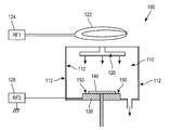
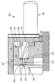
Figure 1 shows a cross section of an
The gas source materials may be introduced into the
The
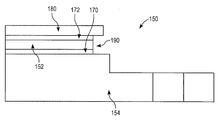
Figure 2 illustrates a portion of a
The
The adhesive bonding layers 170 and 172 are preferably formed of a low modulus material, such as an elastomeric silicone or a silicone rubber material. However, any suitable bonding material can be used. The thickness of the
2, a portion of the
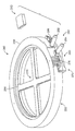
FIG. 3 is a perspective view of a mounting
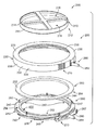
4 is another perspective view of the installed
The
The
The
According to one embodiment, the
When the
5 is a cross-sectional view of a portion of a mounting fixture having an
The
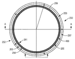
6 and 7, the
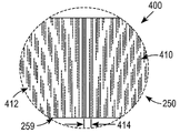
8 is a plan view showing that the clamping
The plurality of
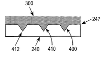
9 is a cross-sectional view of a
According to an exemplary embodiment, each of the plurality of
Each of Figures 10 and 11 is a cross-sectional view of a
According to an exemplary embodiment, the clamping surface on the
As used herein with respect to numerical values, the term " about " can be viewed as representing a numerical value associated with the stated numerical value, including a tolerance of close to +/- 10%.
It should also be understood that when the terms "substantially "," relatively ", and "substantially" are used in connection with geometric shapes, accuracy of geometric shapes is not required but that the latitude of the geometry is within the scope of the present specification. . Geometric terms, "generally," "relatively," and "substantially" encompass features that meet rigid definitions as well as features that are very close to strict definitions.
Although the present invention has been described in connection with the preferred embodiments thereof, it is evident that many alternatives, modifications, and variations will be apparent to those skilled in the art without departing from the spirit and scope of the invention as defined in the appended claims. To those skilled in the art.
Claims (21)
As a mounting unit,
An upper ring having one or more internal threads;
Clamp ring;
A base ring having one or more external threads configured to receive one or more threads of the upper ring, wherein when the upper ring is tightened onto the base ring, the elastomeric band is attached to the lower surface of the clamp ring And the base ring is clamped between a clamping surface configured to release the elastomeric band on at least one of the lower surface of the clamp ring and / or the upper surface of the base ring, Said base ring; And
The mounting unit including a latch and a release mechanism releasing the elastomeric band to the mounting groove by declamping the elastomeric band from between the clamp ring and the base ring; And
And a band loader for positioning the elastomeric band in the mounting unit between the clamp ring and the base ring.
Wherein the clamp ring is an annular ring having an upper section and a lower section forming a step on a lower portion of the clamp ring.
Wherein the latch and release mechanism comprises a first handle attached to an outer edge of the upper ring, a second handle attached to an outer edge of the base ring, and a latch mechanism for securing the upper ring to the base ring. Installation fixtures.
Wherein the clamping surface on at least one of the upper surface of the base ring and / or the lower surface of the clamp ring is a non-tacky coating.
Wherein the clamping surface on at least one of the upper surface of the base ring and / or the lower surface of the clamp ring is a plurality of grooves.
Wherein the lower surface of the clamp ring and the upper surface of the base ring each have a plurality of grooves.
Wherein the plurality of grooves extend radially from an inner edge to an outer edge of the lower surface of the clamp ring and / or from an inner edge to an outer edge of the upper surface of the base ring.
Wherein the plurality of grooves are continuous.
Wherein the plurality of grooves extend circumferentially about an upper surface of the base ring and / or a lower surface of the clamp ring.
Each of the plurality of grooves having an angled recess formed by a first angled surface and a second angled surface, each of the angled recesses having an angle of between about 10 degrees and about 170 degrees between the first angled surface and the second angled surface To form an annular mounting fixture.
Said angled grooves being greater than 90 degrees.
The plurality of grooves having a width from one edge of the groove to a depth of from about 0.0009 to about 0.0039 inches, from about 0.010 to about 0.016 inches, and each of the plurality of grooves being spaced apart from each other by about 0.012 to 0.016 inches Annular mounting fixture.
Wherein the lower surface of the clamp ring and the upper clamping surface and lower clamping surface on the upper surface of the base ring include areas that are not in contact with the elastomeric band when the elastomeric band is not clamped.
The clamping surface on the lower surface of the clamping ring and / or the clamping surface on the upper surface of the base ring may have a larger surface in contact with the elastomeric band when the elastomeric band is clamped than when the elastomeric band is de- / RTI > wherein the annular mounting fixture has an annular mounting fixture.
The plurality of grooves are substantially parallel or concentric.
Wherein the clamp ring and the base ring are made of plastic.
Expanding the elastomeric band in a circular shape having a diameter greater than the diameter of the mounting groove around the substrate support;
Clamping the elastomeric band in an expanded form between a base ring and a clamp ring, wherein at least one of the base ring and the clamp ring includes a plurality of elastomeric bands on the upper surface of the base ring and / Clamping the elastomeric band, the elastomeric band having a clamping surface configured to release the elastomeric band;
Disposing the elastomeric band on the substrate support in the expanded form; And
And releasing the elastomeric band from between the clamp ring and the base ring, the elastomeric band contracting the elastomeric band into the mounting groove of the substrate support.
Wherein clamping the elastomeric band between the base ring and the clamp ring is such that the surface of the elastomeric band in contact with the clamping surface is stretched and the surface is contracted upon de- clamping, Wherein the polymer band is deformed.
Further comprising positioning the elastomeric band adjacent the mounting groove prior to releasing the elastomeric band into the mounting groove.
Wherein expanding the elastomeric band is performed using a band loader that positions the elastomeric band between an upper surface of the base ring and a lower surface of the clamp ring.
Further comprising the step of uniformly expanding said elastomeric band in said circular shape and evenly shrinking said elastomeric band into said mounting groove.
Applications Claiming Priority (2)
| Application Number | Priority Date | Filing Date | Title |
|---|---|---|---|
| US13/930,659 US9502279B2 (en) | 2013-06-28 | 2013-06-28 | Installation fixture having a micro-grooved non-stick surface |
| US13/930,659 | 2013-06-28 |
Publications (1)
| Publication Number | Publication Date |
|---|---|
| KR20150044371A true KR20150044371A (en) | 2015-04-24 |
Family
ID=52115739
Family Applications (1)
| Application Number | Title | Priority Date | Filing Date |
|---|---|---|---|
| KR20140081147A KR20150044371A (en) | 2013-06-28 | 2014-06-30 | Installation fixture having a micro-grooved non-stick surface |
Country Status (5)
| Country | Link |
|---|---|
| US (1) | US9502279B2 (en) |
| JP (1) | JP2015029088A (en) |
| KR (1) | KR20150044371A (en) |
| CN (1) | CN104253078A (en) |
| TW (1) | TWI622123B (en) |
Families Citing this family (4)
| Publication number | Priority date | Publication date | Assignee | Title |
|---|---|---|---|---|
| CN105405797B (en) * | 2015-12-30 | 2018-01-12 | 天津金海通自动化设备制造有限公司 | One kind gives gas relocation mechanism |
| JP6572788B2 (en) * | 2016-01-29 | 2019-09-11 | 住友大阪セメント株式会社 | Electrostatic chuck device |
| JP7340938B2 (en) * | 2019-02-25 | 2023-09-08 | 東京エレクトロン株式会社 | Mounting table and substrate processing equipment |
| CN116845004A (en) * | 2020-05-27 | 2023-10-03 | 北京北方华创微电子装备有限公司 | Semiconductor processing equipment |
Family Cites Families (31)
| Publication number | Priority date | Publication date | Assignee | Title |
|---|---|---|---|---|
| US5636098A (en) | 1994-01-06 | 1997-06-03 | Applied Materials, Inc. | Barrier seal for electrostatic chuck |
| US5740009A (en) | 1996-11-29 | 1998-04-14 | Applied Materials, Inc. | Apparatus for improving wafer and chuck edge protection |
| US6090304A (en) | 1997-08-28 | 2000-07-18 | Lam Research Corporation | Methods for selective plasma etch |
| US6364957B1 (en) | 1997-10-09 | 2002-04-02 | Applied Materials, Inc. | Support assembly with thermal expansion compensation |
| CN100401852C (en) | 2001-04-30 | 2008-07-09 | 科林研发公司 | Method and apparatus for controlling spatial temperature distribution across surface of workpiece support |
| US6771482B2 (en) | 2001-07-30 | 2004-08-03 | Unaxis Usa Inc. | Perimeter seal for backside cooling of substrates |
| JP4451098B2 (en) * | 2002-08-22 | 2010-04-14 | 住友大阪セメント株式会社 | Susceptor device |
| US7252738B2 (en) | 2002-09-20 | 2007-08-07 | Lam Research Corporation | Apparatus for reducing polymer deposition on a substrate and substrate support |
| JP4247625B2 (en) | 2002-10-25 | 2009-04-02 | Nok株式会社 | Plasma-resistant seal |
| US6944006B2 (en) | 2003-04-03 | 2005-09-13 | Applied Materials, Inc. | Guard for electrostatic chuck |
| US7514506B2 (en) | 2004-03-31 | 2009-04-07 | Greene, Tweed Of Delaware, Inc. | Fast curing fluoroelastomeric compositions, adhesive fluoroelastomeric compositions and methods for bonding fluoroelastomeric compositions |
| US8038796B2 (en) | 2004-12-30 | 2011-10-18 | Lam Research Corporation | Apparatus for spatial and temporal control of temperature on a substrate |
| US7319316B2 (en) | 2005-06-29 | 2008-01-15 | Lam Research Corporation | Apparatus for measuring a set of electrical characteristics in a plasma |
| US7431788B2 (en) * | 2005-07-19 | 2008-10-07 | Lam Research Corporation | Method of protecting a bond layer in a substrate support adapted for use in a plasma processing system |
| JP2007207728A (en) * | 2006-02-06 | 2007-08-16 | Aisin Seiki Co Ltd | Separator for polymer electrolyte fuel cell, its manufacturing method, and polymer electrolyte fuel cell |
| GB0610479D0 (en) | 2006-05-26 | 2006-07-05 | Ge Healthcare Bio Sciences Ab | A method for generating metal chelating affinity ligands |
| US20090179366A1 (en) | 2008-01-16 | 2009-07-16 | Sokudo Co., Ltd. | Apparatus for supporting a substrate during semiconductor processing operations |
| KR101625516B1 (en) * | 2008-02-08 | 2016-05-30 | 램 리써치 코포레이션 | Plasma processing apparatus and method of processing a semiconductor substrate in the same |
| CN201167837Y (en) * | 2008-03-06 | 2008-12-24 | 浙江爱仕达电器股份有限公司 | Aluminium alloy anode oxide physical non-stick pan |
| US7884925B2 (en) | 2008-05-23 | 2011-02-08 | Lam Research Corporation | Electrical and optical system and methods for monitoring erosion of electrostatic chuck edge bead materials |
| US8469368B2 (en) | 2008-08-19 | 2013-06-25 | Lam Research Corporation | Edge rings for electrostatic chucks |
| JP5635001B2 (en) | 2008-09-26 | 2014-12-03 | ラム リサーチ コーポレーションLam Research Corporation | Thermal contact between electrostatic chuck and hot edge ring adjustable by clocking the coupling ring |
| EP2342951B1 (en) | 2008-10-31 | 2019-03-06 | Lam Research Corporation | Lower electrode assembly of plasma processing chamber |
| US20100117309A1 (en) | 2008-11-13 | 2010-05-13 | Applied Materials, Inc. | Sealing apparatus for a process chamber |
| US8409995B2 (en) | 2009-08-07 | 2013-04-02 | Tokyo Electron Limited | Substrate processing apparatus, positioning method and focus ring installation method |
| JP5291039B2 (en) * | 2010-03-31 | 2013-09-18 | 大日本スクリーン製造株式会社 | Substrate holding and rotating device and substrate processing apparatus |
| TWM431430U (en) * | 2011-08-24 | 2012-06-11 | Wafer Works Corp | Clip board type fastening device for use in annularly etching wafer |
| US9869392B2 (en) * | 2011-10-20 | 2018-01-16 | Lam Research Corporation | Edge seal for lower electrode assembly |
| US8844106B2 (en) * | 2011-11-10 | 2014-09-30 | Lam Research Corporation | Installation fixture for elastomer bands and methods of using the same |
| US8677586B2 (en) * | 2012-04-04 | 2014-03-25 | Lam Research Corporation | Installation fixture for elastomer bands and methods of using the same |
| US9583377B2 (en) * | 2013-12-17 | 2017-02-28 | Lam Research Corporation | Installation fixture for elastomer bands |
-
2013
- 2013-06-28 US US13/930,659 patent/US9502279B2/en active Active
-
2014
- 2014-06-27 TW TW103122372A patent/TWI622123B/en active
- 2014-06-27 JP JP2014132168A patent/JP2015029088A/en active Pending
- 2014-06-30 CN CN201410306477.2A patent/CN104253078A/en active Pending
- 2014-06-30 KR KR20140081147A patent/KR20150044371A/en not_active Application Discontinuation
Also Published As
| Publication number | Publication date |
|---|---|
| JP2015029088A (en) | 2015-02-12 |
| US20150003903A1 (en) | 2015-01-01 |
| TWI622123B (en) | 2018-04-21 |
| US9502279B2 (en) | 2016-11-22 |
| TW201516278A (en) | 2015-05-01 |
| CN104253078A (en) | 2014-12-31 |
Similar Documents
| Publication | Publication Date | Title |
|---|---|---|
| KR102551996B1 (en) | Permanent secondary erosion containment for electrostatic chuck bonds | |
| US8677586B2 (en) | Installation fixture for elastomer bands and methods of using the same | |
| TWI415165B (en) | Method of protecting a bond layer in a substrate support adapted for use in a plasma processing system | |
| KR102282723B1 (en) | Installation fixture for elastomer bands | |
| US10804081B2 (en) | Edge ring dimensioned to extend lifetime of elastomer seal in a plasma processing chamber | |
| US9859142B2 (en) | Edge seal for lower electrode assembly | |
| US20130340942A1 (en) | Edge seal for lower electrode assembly | |
| US9355884B2 (en) | Installation fixture for elastomer bands and methods of using the same | |
| KR20150044371A (en) | Installation fixture having a micro-grooved non-stick surface |
Legal Events
| Date | Code | Title | Description |
|---|---|---|---|
| WITN | Withdrawal due to no request for examination |