KR20150040234A - Methods for depositing silicon nitride films - Google Patents
Methods for depositing silicon nitride films Download PDFInfo
- Publication number
- KR20150040234A KR20150040234A KR20140133394A KR20140133394A KR20150040234A KR 20150040234 A KR20150040234 A KR 20150040234A KR 20140133394 A KR20140133394 A KR 20140133394A KR 20140133394 A KR20140133394 A KR 20140133394A KR 20150040234 A KR20150040234 A KR 20150040234A
- Authority
- KR
- South Korea
- Prior art keywords
- plasma
- reactor
- silicon nitride
- group
- nitrogen
- Prior art date
Links
Images


Classifications
-
- C—CHEMISTRY; METALLURGY
- C07—ORGANIC CHEMISTRY
- C07F—ACYCLIC, CARBOCYCLIC OR HETEROCYCLIC COMPOUNDS CONTAINING ELEMENTS OTHER THAN CARBON, HYDROGEN, HALOGEN, OXYGEN, NITROGEN, SULFUR, SELENIUM OR TELLURIUM
- C07F7/00—Compounds containing elements of Groups 4 or 14 of the Periodic System
- C07F7/02—Silicon compounds
- C07F7/08—Compounds having one or more C—Si linkages
- C07F7/10—Compounds having one or more C—Si linkages containing nitrogen having a Si-N linkage
-
- H—ELECTRICITY
- H01—ELECTRIC ELEMENTS
- H01L—SEMICONDUCTOR DEVICES NOT COVERED BY CLASS H10
- H01L21/00—Processes or apparatus adapted for the manufacture or treatment of semiconductor or solid state devices or of parts thereof
- H01L21/02—Manufacture or treatment of semiconductor devices or of parts thereof
- H01L21/02104—Forming layers
- H01L21/02107—Forming insulating materials on a substrate
- H01L21/02109—Forming insulating materials on a substrate characterised by the type of layer, e.g. type of material, porous/non-porous, pre-cursors, mixtures or laminates
- H01L21/02112—Forming insulating materials on a substrate characterised by the type of layer, e.g. type of material, porous/non-porous, pre-cursors, mixtures or laminates characterised by the material of the layer
- H01L21/02123—Forming insulating materials on a substrate characterised by the type of layer, e.g. type of material, porous/non-porous, pre-cursors, mixtures or laminates characterised by the material of the layer the material containing silicon
- H01L21/0217—Forming insulating materials on a substrate characterised by the type of layer, e.g. type of material, porous/non-porous, pre-cursors, mixtures or laminates characterised by the material of the layer the material containing silicon the material being a silicon nitride not containing oxygen, e.g. SixNy or SixByNz
-
- C—CHEMISTRY; METALLURGY
- C23—COATING METALLIC MATERIAL; COATING MATERIAL WITH METALLIC MATERIAL; CHEMICAL SURFACE TREATMENT; DIFFUSION TREATMENT OF METALLIC MATERIAL; COATING BY VACUUM EVAPORATION, BY SPUTTERING, BY ION IMPLANTATION OR BY CHEMICAL VAPOUR DEPOSITION, IN GENERAL; INHIBITING CORROSION OF METALLIC MATERIAL OR INCRUSTATION IN GENERAL
- C23C—COATING METALLIC MATERIAL; COATING MATERIAL WITH METALLIC MATERIAL; SURFACE TREATMENT OF METALLIC MATERIAL BY DIFFUSION INTO THE SURFACE, BY CHEMICAL CONVERSION OR SUBSTITUTION; COATING BY VACUUM EVAPORATION, BY SPUTTERING, BY ION IMPLANTATION OR BY CHEMICAL VAPOUR DEPOSITION, IN GENERAL
- C23C14/00—Coating by vacuum evaporation, by sputtering or by ion implantation of the coating forming material
- C23C14/02—Pretreatment of the material to be coated
- C23C14/027—Graded interfaces
-
- C—CHEMISTRY; METALLURGY
- C23—COATING METALLIC MATERIAL; COATING MATERIAL WITH METALLIC MATERIAL; CHEMICAL SURFACE TREATMENT; DIFFUSION TREATMENT OF METALLIC MATERIAL; COATING BY VACUUM EVAPORATION, BY SPUTTERING, BY ION IMPLANTATION OR BY CHEMICAL VAPOUR DEPOSITION, IN GENERAL; INHIBITING CORROSION OF METALLIC MATERIAL OR INCRUSTATION IN GENERAL
- C23C—COATING METALLIC MATERIAL; COATING MATERIAL WITH METALLIC MATERIAL; SURFACE TREATMENT OF METALLIC MATERIAL BY DIFFUSION INTO THE SURFACE, BY CHEMICAL CONVERSION OR SUBSTITUTION; COATING BY VACUUM EVAPORATION, BY SPUTTERING, BY ION IMPLANTATION OR BY CHEMICAL VAPOUR DEPOSITION, IN GENERAL
- C23C14/00—Coating by vacuum evaporation, by sputtering or by ion implantation of the coating forming material
- C23C14/22—Coating by vacuum evaporation, by sputtering or by ion implantation of the coating forming material characterised by the process of coating
- C23C14/54—Controlling or regulating the coating process
- C23C14/548—Controlling the composition
-
- C—CHEMISTRY; METALLURGY
- C23—COATING METALLIC MATERIAL; COATING MATERIAL WITH METALLIC MATERIAL; CHEMICAL SURFACE TREATMENT; DIFFUSION TREATMENT OF METALLIC MATERIAL; COATING BY VACUUM EVAPORATION, BY SPUTTERING, BY ION IMPLANTATION OR BY CHEMICAL VAPOUR DEPOSITION, IN GENERAL; INHIBITING CORROSION OF METALLIC MATERIAL OR INCRUSTATION IN GENERAL
- C23C—COATING METALLIC MATERIAL; COATING MATERIAL WITH METALLIC MATERIAL; SURFACE TREATMENT OF METALLIC MATERIAL BY DIFFUSION INTO THE SURFACE, BY CHEMICAL CONVERSION OR SUBSTITUTION; COATING BY VACUUM EVAPORATION, BY SPUTTERING, BY ION IMPLANTATION OR BY CHEMICAL VAPOUR DEPOSITION, IN GENERAL
- C23C16/00—Chemical coating by decomposition of gaseous compounds, without leaving reaction products of surface material in the coating, i.e. chemical vapour deposition [CVD] processes
- C23C16/06—Chemical coating by decomposition of gaseous compounds, without leaving reaction products of surface material in the coating, i.e. chemical vapour deposition [CVD] processes characterised by the deposition of metallic material
- C23C16/18—Chemical coating by decomposition of gaseous compounds, without leaving reaction products of surface material in the coating, i.e. chemical vapour deposition [CVD] processes characterised by the deposition of metallic material from metallo-organic compounds
-
- C—CHEMISTRY; METALLURGY
- C23—COATING METALLIC MATERIAL; COATING MATERIAL WITH METALLIC MATERIAL; CHEMICAL SURFACE TREATMENT; DIFFUSION TREATMENT OF METALLIC MATERIAL; COATING BY VACUUM EVAPORATION, BY SPUTTERING, BY ION IMPLANTATION OR BY CHEMICAL VAPOUR DEPOSITION, IN GENERAL; INHIBITING CORROSION OF METALLIC MATERIAL OR INCRUSTATION IN GENERAL
- C23C—COATING METALLIC MATERIAL; COATING MATERIAL WITH METALLIC MATERIAL; SURFACE TREATMENT OF METALLIC MATERIAL BY DIFFUSION INTO THE SURFACE, BY CHEMICAL CONVERSION OR SUBSTITUTION; COATING BY VACUUM EVAPORATION, BY SPUTTERING, BY ION IMPLANTATION OR BY CHEMICAL VAPOUR DEPOSITION, IN GENERAL
- C23C16/00—Chemical coating by decomposition of gaseous compounds, without leaving reaction products of surface material in the coating, i.e. chemical vapour deposition [CVD] processes
- C23C16/22—Chemical coating by decomposition of gaseous compounds, without leaving reaction products of surface material in the coating, i.e. chemical vapour deposition [CVD] processes characterised by the deposition of inorganic material, other than metallic material
- C23C16/30—Deposition of compounds, mixtures or solid solutions, e.g. borides, carbides, nitrides
- C23C16/34—Nitrides
- C23C16/345—Silicon nitride
-
- C—CHEMISTRY; METALLURGY
- C23—COATING METALLIC MATERIAL; COATING MATERIAL WITH METALLIC MATERIAL; CHEMICAL SURFACE TREATMENT; DIFFUSION TREATMENT OF METALLIC MATERIAL; COATING BY VACUUM EVAPORATION, BY SPUTTERING, BY ION IMPLANTATION OR BY CHEMICAL VAPOUR DEPOSITION, IN GENERAL; INHIBITING CORROSION OF METALLIC MATERIAL OR INCRUSTATION IN GENERAL
- C23C—COATING METALLIC MATERIAL; COATING MATERIAL WITH METALLIC MATERIAL; SURFACE TREATMENT OF METALLIC MATERIAL BY DIFFUSION INTO THE SURFACE, BY CHEMICAL CONVERSION OR SUBSTITUTION; COATING BY VACUUM EVAPORATION, BY SPUTTERING, BY ION IMPLANTATION OR BY CHEMICAL VAPOUR DEPOSITION, IN GENERAL
- C23C16/00—Chemical coating by decomposition of gaseous compounds, without leaving reaction products of surface material in the coating, i.e. chemical vapour deposition [CVD] processes
- C23C16/44—Chemical coating by decomposition of gaseous compounds, without leaving reaction products of surface material in the coating, i.e. chemical vapour deposition [CVD] processes characterised by the method of coating
- C23C16/455—Chemical coating by decomposition of gaseous compounds, without leaving reaction products of surface material in the coating, i.e. chemical vapour deposition [CVD] processes characterised by the method of coating characterised by the method used for introducing gases into reaction chamber or for modifying gas flows in reaction chamber
- C23C16/45523—Pulsed gas flow or change of composition over time
- C23C16/45525—Atomic layer deposition [ALD]
- C23C16/45527—Atomic layer deposition [ALD] characterized by the ALD cycle, e.g. different flows or temperatures during half-reactions, unusual pulsing sequence, use of precursor mixtures or auxiliary reactants or activations
- C23C16/45536—Use of plasma, radiation or electromagnetic fields
- C23C16/45542—Plasma being used non-continuously during the ALD reactions
-
- C—CHEMISTRY; METALLURGY
- C23—COATING METALLIC MATERIAL; COATING MATERIAL WITH METALLIC MATERIAL; CHEMICAL SURFACE TREATMENT; DIFFUSION TREATMENT OF METALLIC MATERIAL; COATING BY VACUUM EVAPORATION, BY SPUTTERING, BY ION IMPLANTATION OR BY CHEMICAL VAPOUR DEPOSITION, IN GENERAL; INHIBITING CORROSION OF METALLIC MATERIAL OR INCRUSTATION IN GENERAL
- C23C—COATING METALLIC MATERIAL; COATING MATERIAL WITH METALLIC MATERIAL; SURFACE TREATMENT OF METALLIC MATERIAL BY DIFFUSION INTO THE SURFACE, BY CHEMICAL CONVERSION OR SUBSTITUTION; COATING BY VACUUM EVAPORATION, BY SPUTTERING, BY ION IMPLANTATION OR BY CHEMICAL VAPOUR DEPOSITION, IN GENERAL
- C23C16/00—Chemical coating by decomposition of gaseous compounds, without leaving reaction products of surface material in the coating, i.e. chemical vapour deposition [CVD] processes
- C23C16/44—Chemical coating by decomposition of gaseous compounds, without leaving reaction products of surface material in the coating, i.e. chemical vapour deposition [CVD] processes characterised by the method of coating
- C23C16/455—Chemical coating by decomposition of gaseous compounds, without leaving reaction products of surface material in the coating, i.e. chemical vapour deposition [CVD] processes characterised by the method of coating characterised by the method used for introducing gases into reaction chamber or for modifying gas flows in reaction chamber
- C23C16/45523—Pulsed gas flow or change of composition over time
- C23C16/45525—Atomic layer deposition [ALD]
- C23C16/45553—Atomic layer deposition [ALD] characterized by the use of precursors specially adapted for ALD
-
- C—CHEMISTRY; METALLURGY
- C23—COATING METALLIC MATERIAL; COATING MATERIAL WITH METALLIC MATERIAL; CHEMICAL SURFACE TREATMENT; DIFFUSION TREATMENT OF METALLIC MATERIAL; COATING BY VACUUM EVAPORATION, BY SPUTTERING, BY ION IMPLANTATION OR BY CHEMICAL VAPOUR DEPOSITION, IN GENERAL; INHIBITING CORROSION OF METALLIC MATERIAL OR INCRUSTATION IN GENERAL
- C23C—COATING METALLIC MATERIAL; COATING MATERIAL WITH METALLIC MATERIAL; SURFACE TREATMENT OF METALLIC MATERIAL BY DIFFUSION INTO THE SURFACE, BY CHEMICAL CONVERSION OR SUBSTITUTION; COATING BY VACUUM EVAPORATION, BY SPUTTERING, BY ION IMPLANTATION OR BY CHEMICAL VAPOUR DEPOSITION, IN GENERAL
- C23C28/00—Coating for obtaining at least two superposed coatings either by methods not provided for in a single one of groups C23C2/00 - C23C26/00 or by combinations of methods provided for in subclasses C23C and C25C or C25D
- C23C28/40—Coatings including alternating layers following a pattern, a periodic or defined repetition
- C23C28/42—Coatings including alternating layers following a pattern, a periodic or defined repetition characterized by the composition of the alternating layers
-
- H—ELECTRICITY
- H01—ELECTRIC ELEMENTS
- H01L—SEMICONDUCTOR DEVICES NOT COVERED BY CLASS H10
- H01L21/00—Processes or apparatus adapted for the manufacture or treatment of semiconductor or solid state devices or of parts thereof
- H01L21/02—Manufacture or treatment of semiconductor devices or of parts thereof
- H01L21/02104—Forming layers
- H01L21/02107—Forming insulating materials on a substrate
- H01L21/02109—Forming insulating materials on a substrate characterised by the type of layer, e.g. type of material, porous/non-porous, pre-cursors, mixtures or laminates
- H01L21/02205—Forming insulating materials on a substrate characterised by the type of layer, e.g. type of material, porous/non-porous, pre-cursors, mixtures or laminates the layer being characterised by the precursor material for deposition
- H01L21/02208—Forming insulating materials on a substrate characterised by the type of layer, e.g. type of material, porous/non-porous, pre-cursors, mixtures or laminates the layer being characterised by the precursor material for deposition the precursor containing a compound comprising Si
- H01L21/02211—Forming insulating materials on a substrate characterised by the type of layer, e.g. type of material, porous/non-porous, pre-cursors, mixtures or laminates the layer being characterised by the precursor material for deposition the precursor containing a compound comprising Si the compound being a silane, e.g. disilane, methylsilane or chlorosilane
-
- H—ELECTRICITY
- H01—ELECTRIC ELEMENTS
- H01L—SEMICONDUCTOR DEVICES NOT COVERED BY CLASS H10
- H01L21/00—Processes or apparatus adapted for the manufacture or treatment of semiconductor or solid state devices or of parts thereof
- H01L21/02—Manufacture or treatment of semiconductor devices or of parts thereof
- H01L21/02104—Forming layers
- H01L21/02107—Forming insulating materials on a substrate
- H01L21/02109—Forming insulating materials on a substrate characterised by the type of layer, e.g. type of material, porous/non-porous, pre-cursors, mixtures or laminates
- H01L21/02205—Forming insulating materials on a substrate characterised by the type of layer, e.g. type of material, porous/non-porous, pre-cursors, mixtures or laminates the layer being characterised by the precursor material for deposition
- H01L21/02208—Forming insulating materials on a substrate characterised by the type of layer, e.g. type of material, porous/non-porous, pre-cursors, mixtures or laminates the layer being characterised by the precursor material for deposition the precursor containing a compound comprising Si
- H01L21/02219—Forming insulating materials on a substrate characterised by the type of layer, e.g. type of material, porous/non-porous, pre-cursors, mixtures or laminates the layer being characterised by the precursor material for deposition the precursor containing a compound comprising Si the compound comprising silicon and nitrogen
- H01L21/02222—Forming insulating materials on a substrate characterised by the type of layer, e.g. type of material, porous/non-porous, pre-cursors, mixtures or laminates the layer being characterised by the precursor material for deposition the precursor containing a compound comprising Si the compound comprising silicon and nitrogen the compound being a silazane
-
- H—ELECTRICITY
- H01—ELECTRIC ELEMENTS
- H01L—SEMICONDUCTOR DEVICES NOT COVERED BY CLASS H10
- H01L21/00—Processes or apparatus adapted for the manufacture or treatment of semiconductor or solid state devices or of parts thereof
- H01L21/02—Manufacture or treatment of semiconductor devices or of parts thereof
- H01L21/02104—Forming layers
- H01L21/02107—Forming insulating materials on a substrate
- H01L21/02225—Forming insulating materials on a substrate characterised by the process for the formation of the insulating layer
- H01L21/0226—Forming insulating materials on a substrate characterised by the process for the formation of the insulating layer formation by a deposition process
- H01L21/02263—Forming insulating materials on a substrate characterised by the process for the formation of the insulating layer formation by a deposition process deposition from the gas or vapour phase
- H01L21/02271—Forming insulating materials on a substrate characterised by the process for the formation of the insulating layer formation by a deposition process deposition from the gas or vapour phase deposition by decomposition or reaction of gaseous or vapour phase compounds, i.e. chemical vapour deposition
- H01L21/02274—Forming insulating materials on a substrate characterised by the process for the formation of the insulating layer formation by a deposition process deposition from the gas or vapour phase deposition by decomposition or reaction of gaseous or vapour phase compounds, i.e. chemical vapour deposition in the presence of a plasma [PECVD]
-
- H—ELECTRICITY
- H01—ELECTRIC ELEMENTS
- H01L—SEMICONDUCTOR DEVICES NOT COVERED BY CLASS H10
- H01L21/00—Processes or apparatus adapted for the manufacture or treatment of semiconductor or solid state devices or of parts thereof
- H01L21/02—Manufacture or treatment of semiconductor devices or of parts thereof
- H01L21/02104—Forming layers
- H01L21/02107—Forming insulating materials on a substrate
- H01L21/02225—Forming insulating materials on a substrate characterised by the process for the formation of the insulating layer
- H01L21/0226—Forming insulating materials on a substrate characterised by the process for the formation of the insulating layer formation by a deposition process
- H01L21/02263—Forming insulating materials on a substrate characterised by the process for the formation of the insulating layer formation by a deposition process deposition from the gas or vapour phase
- H01L21/02271—Forming insulating materials on a substrate characterised by the process for the formation of the insulating layer formation by a deposition process deposition from the gas or vapour phase deposition by decomposition or reaction of gaseous or vapour phase compounds, i.e. chemical vapour deposition
- H01L21/0228—Forming insulating materials on a substrate characterised by the process for the formation of the insulating layer formation by a deposition process deposition from the gas or vapour phase deposition by decomposition or reaction of gaseous or vapour phase compounds, i.e. chemical vapour deposition deposition by cyclic CVD, e.g. ALD, ALE, pulsed CVD
Abstract
Description
관련 출원의 전후 참조Before and after reference of related application
본 출원은 충분히 기재된 바와 같이 본원에 참조로서 포함된 2013년 10월 3일 출원된 미국 가특허출원 61/886,406호의 이익을 주장한다.This application claims the benefit of U.S. Provisional Patent Application 61 / 886,406, filed October 3, 2013, which is hereby incorporated by reference as if fully set forth.
하나 이상의 오가노아미노실란 전구체를 이용하여 등각의 화학량론적 또는 비-화학량론적 질화규소 막을 증착시키는 방법이 본원에 기재된다. 보다 구체적으로, 집적 회로 디바이스의 제작에서의 질화규소 막을 증착시키는데 이용되는 플라즈마 강화 원자층 증착 ("PEALD"), 플라즈마 강화 사이클릭 화학적 증기 증착 ("PECCVD")을 비제한적으로 포함하는 플라즈마-기반 공정이 본원에 기재된다.Methods for depositing conformal stoichiometric or non-stoichiometric silicon nitride films using one or more organoaminosilane precursors are described herein. More particularly, plasma-based processes (including but not limited to plasma enhanced atomic layer deposition ("PEALD"), plasma enhanced cyclic chemical vapor deposition ("PECCVD") used to deposit silicon nitride films in the fabrication of integrated circuit devices Are described herein.
저압 화학적 증기 증착 (LPCVD) 공정은 질화규소 막의 증착을 위해 반도체 산업에서 이용되는 더욱 광범하게 인정되는 방법들 중 하나이다. 암모니아를 이용한 저압 화학적 증기 증착 (LPCVD)은 합리적인 성장률 및 균일성을 얻기 위해 650℃가 넘는 증착 온도를 필요로 할 수 있다. 개선된 막 특성을 제공하기 위해 통상적으로 더 높은 증착 온도가 이용된다. 질화규소를 증가시키기 위해 더욱 일반적인 산업 방법들 중 하나는 전구체 실란, 디클로로실란, 및/또는 암모니아를 이용하여 750℃를 초과하는 온도의 고온 벽 반응기에서 저압 화학적 증기 증착을 통해 수행된다. 그러나, 이러한 방법을 이용하는 경우 여러 단점이 존재한다. 예를 들어, 특정 전구체, 예컨대 실란은 자연발화성이다. 이는 조작 및 용법에 문제를 야기할 수 있다. 또한, 디클로로실란으로부터 증착된 막은 증착 공정 동안 부산물로서 형성되는 염소 및 암모늄 클로라이드와 같은 특정 불순물을 함유할 수 있다.Low pressure chemical vapor deposition (LPCVD) processes are one of the more widely accepted methods used in the semiconductor industry for the deposition of silicon nitride films. Low pressure chemical vapor deposition (LPCVD) using ammonia may require deposition temperatures in excess of 650 [deg.] C to achieve reasonable growth rates and uniformity. Higher deposition temperatures are typically used to provide improved film properties. One of the more common industrial methods to increase silicon nitride is through low pressure chemical vapor deposition in a high temperature wall reactor at temperatures above 750 DEG C using precursor silane, dichlorosilane, and / or ammonia. However, there are various drawbacks when using this method. For example, certain precursors, such as silanes, are pyrophoric. This can cause problems with operation and usage. In addition, the film deposited from the dichlorosilane may contain certain impurities, such as chlorine and ammonium chloride, formed as a by-product during the deposition process.
BTBAS 및 클로로실란과 같이 질화규소 막을 증착시키는데 이용되는 전구체는 일반적으로 550℃가 넘는 온도에서 막을 증착시킨다. 반도체 디바이스의 소형화 및 낮은 열 예산의 경향은 400℃ 미만의 공정 온도 및 더욱 높은 증착률을 요구한다. 실리콘 막이 증착되는 온도는, 특히 금속화 층을 포함하는 기판에 대해 그리고 다수의 III-V족 및 II-VI족 디바이스 상에서, 격자에서의 이온 확산을 방지하기 위해 감소되어야 한다. The precursors used to deposit silicon nitride films, such as BTBAS and chlorosilanes, generally deposit films at temperatures above 550 ° C. The miniaturization of semiconductor devices and the trend of low thermal budgets require process temperatures of less than 400 DEG C and higher deposition rates. The temperature at which the silicon film is deposited must be reduced to prevent ion diffusion in the lattice, especially for the substrate comprising the metallization layer and on many of the III-V and II-VI devices.
미국 공개공보 2013/183835호 ("'835 공개공보")는 기판 상의 낮은 온도에서 등각의 질화규소 막을 형성하기 위한 방법 및 장치를 기재하고 있다. 질화규소 층을 형성하는 방법은 공정 가스 혼합물을 그 안에 기판을 지닌 공정 챔버로 유동시키고 (이 때 공정 가스 혼합물은 불안정한 규소-질소 결합, 규소-탄소 결합, 또는 질소-탄소 결합을 지니는 전구체 가스 분자를 포함한다), 불안정한 결합을 우선적으로 끊어서 전구체 가스를 약 20℃ 내지 약 480℃의 온도에서 활성화시킴에 의해 전구체 가스 분자를 따라 하나 이상의 반응 부위를 제공하고, 전구체 물질층을 기판 상에 형성하고 (이 때 활성화된 전구체 가스 분자는 하나 이상의 반응 부위에서 기판 상의 표면에 결합한다), 전구체 물질층 상에서 플라즈마 처리 공정을 수행하여 등각의 질화규소 층을 형성하는 것을 포함하는 증착 사이클을 수행하는 것을 포함한다. '835 공개공보는 공정 가스 혼합물이 암모니아, 하이드라진, 헬륨, 아르곤, 수소, 질소, 제논, 및 헬륨을 추가로 포함할 수 있음을 교시한다 ('835 공개공보의 [0031]을 참조하라). '835호는 아르곤 및 헬륨이 더 높은 출력 (예컨대, 1 W/cm2 초과)에서 공정 가스 혼합물에 사용하기에 덜 바람직할 수 있는데, 그 이유는 이것이 플라즈마 상태에서 너무나 반응성이어서 (단지 불안정한 결합의 파괴를 돕는 대신(id.) 전구체 분자의 과도한 분리를 유도할 수 있기 때문이라고 추가로 교시한다. U.S. Publication No. 2013/183835 ("'835 publication") describes a method and apparatus for forming a conformal silicon nitride film at low temperatures on a substrate. A method of forming a silicon nitride layer includes flowing a process gas mixture into a process chamber having a substrate therein wherein the process gas mixture comprises a precursor gas molecule having an unstable silicon-nitrogen bond, a silicon-carbon bond, or a nitrogen- To provide at least one reactive site along the precursor gas molecules by preferentially breaking the labile bonds to activate the precursor gas at a temperature between about 20 [deg.] C and about 480 [deg.] C, to form a layer of precursor material on the substrate Wherein the activated precursor gas molecules are bound to the surface on the substrate at one or more reaction sites), and performing a plasma treatment process on the precursor material layer to form a conformal silicon nitride layer. The '835 publication teaches that the process gas mixture may additionally include ammonia, hydrazine, helium, argon, hydrogen, nitrogen, xenon, and helium (see [835]). '835 may be less desirable for use in process gas mixtures at higher power (eg, greater than 1 W / cm 2 ) because argon and helium are too reactive in the plasma state (Id.) Can lead to excessive separation of the precursor molecules.
미국 공개공보 2009/075490호 ("'490 공개공보")는 실리콘 웨이퍼를 반응 챔버에 도입시키고; 질화규소 화합물을 반응 챔버에 도입시키고; 반응 챔버를 불활성 가스로 퍼징하고; 가스 형태의 질소-함유 공-반응물을 실리콘 웨이퍼 상에서 질화규소 막의 단분자층을 형성하기에 적합한 조건하에 반응 챔버에 도입시키는 것을 포함하는 질화규소 막을 제조하는 방법을 기재하고 있다.U. S. Laid-Open Publication No. 2009/075490 ("'490 publication") introduces a silicon wafer into a reaction chamber; Introducing a silicon nitride compound into the reaction chamber; Purging the reaction chamber with an inert gas; Introducing a nitrogen-containing co-reactant in gaseous form into a reaction chamber under conditions suitable for forming a monolayer of silicon nitride film on a silicon wafer.
미국 공개공보 2009/155606호 ("'606 공개공보")는 기판 상에 질화규소 막을 증착시키는 주기적 방법을 기재하고 있다. 한 구체예에서, 방법은 클로로실란을 기판이 가공되는 반응기에 공급하고; 퍼지 가스를 반응기에 공급하고; 암모니아 플라즈마를 반응기에 제공하는 것을 포함한다.US Publication No. 2009/155606 ("'606 publication") describes a cyclic method of depositing a silicon nitride film on a substrate. In one embodiment, the method comprises supplying chlorosilane to a reactor in which the substrate is processed; Supplying a purge gas to the reactor; And providing an ammonia plasma to the reactor.
미국 특허 6,391,803호 ("'803 특허")는 Si를 함유하는 고형 박막층을 형성하는 원자층 증착 방법을 기재하고 있다. U. S. Patent No. 6,391, 803 ("the '803 patent") describes a method of atomic layer deposition that forms a solid thin film layer containing Si.
미국 특허 6,528,430호 ("'430 특허")는 Si2Cl6 및 NH3, 또는 Si2Cl6 및 활성화된 NH3를 반응물로서 이용하는 질화규소 박막을 형성하는 ALD 방법을 기재하고 있다. 상기 방법의 한 구체예에서, NH3 반응물은 플라즈마를 형성하기 위한 원격 플라즈마 발생기에서 발생하여 Ar 캐리어 가스 스트림 중에서 챔버로 도입된다 ('430 특허 컬럼 4, 56-62행을 참조하라). U.S. Patent No. 6,528,430 (the "'430 patent") describes an ALD process for forming silicon nitride thin films using Si 2 Cl 6 and NH 3 , or Si 2 Cl 6 and activated NH 3 as reactants. In one embodiment of the method, the NH 3 reactant is generated in a remote plasma generator to form a plasma and is introduced into the chamber in an Ar carrier gas stream (see the '430 patent, patent 4, lines 56-62).
미국 공개공보 2010/0081293호 ("'293 공개공보")는 규소 전구체 및 라디칼 질소 전구체를 증착 챔버에 도입시키는 것을 포함하는 질화규소를 증착시키는 방법을 기재하고 있다. 규소 전구체는 N―"Si―"H 결합, N―"Si―"Si 결합 및/또는 Si―"Si―"H 결합을 지닌다. 라디칼 질소 전구체는 포함된 산소로부터 실질적으로 자유롭다. 라디칼 질소 전구체는 증착 챔버 외부에서 발생한다. 규소 전구체 및 라디칼 질소 전구체는 상호작용하여 질화규소 기반 유전체층을 형성한다. '293 공개공보는 Ne, Ar, Kr, 및/또는 Xe로부터 선택되는 출발 물질로부터 증착 챔버 외부에서 발생할 수 있는 라디칼 불활성 가스 전구체의 이용을 추가로 교시한다 ('293 공개공보의 [0027]-[0028] 및 청구항 17을 참조하라). 라디칼 불활성 전구체는 N, NH, 및 NH2로부터 선택되는 라디칼 질소 전구체와 함께 규소 탄소 기반 유전체층을 증착시키거나 질화규소 기반 유전체층을 증착시키는데 이용될 수 있다 (id. 청구항 4를 참조하라). U.S. Publication No. 2010/0081293 ("'293 Open Publication") describes a method of depositing silicon nitride including introducing a silicon precursor and a radical nitrogen precursor into a deposition chamber. The silicon precursor has an N- "Si-" H bond, an N- "Si-" Si bond and / or a Si- "Si-" H bond. The radical nitrogen precursor is substantially free from the contained oxygen. A radical nitrogen precursor occurs outside the deposition chamber. The silicon precursor and the radical nitrogen precursor interact to form a silicon nitride based dielectric layer. The '293 publication further teaches the use of radical inert gas precursors that can occur outside the deposition chamber from starting materials selected from Ne, Ar, Kr, and / or Xe (see [293] - [ 0028] and claim 17). The radical inert precursor may be used to deposit a silicon carbon based dielectric layer with a radical nitrogen precursor selected from N, NH, and NH 2 , or to deposit a silicon nitride based dielectric layer (see id.
미국 공개공보 2012/196048호 ("'048 공개공보")는 전구체를 기판 상에 흡착시키는 공정 및 반응물 가스 및 플라즈마를 이용하여 흡착된 표면을 처리하는 공정을 각각 다수 회 교대시킴으로써 박막을 형성하는 방법을 기재하고 있고, 이 때 반응물 가스는 기판 위에 실질적으로 균일하게 공급되고, 플라즈마는 펄스-시간-조절되어 반응물 가스를 공급하는 공정에 적용된다.U.S. Publication No. 2012/196048 ("'048 Open Publication") discloses a method of forming a thin film by alternately repeating a process of adsorbing a precursor on a substrate and a process of treating a surface adsorbed using a reactant gas and a plasma, Wherein the reactant gas is supplied substantially uniformly over the substrate, and the plasma is applied to the process of pulse-time-regulating the reactant gas supply.
Klaus 등에 의한 "Atomic layer controlled growth of Si3N4 films using sequential surface reactions"라는 명칭의 참조문헌[Surface Science 418: L14-L19 (1998)]은 순차적인 표면 화학 반응을 이용하여 Si(100) 기판 상에서 원자층 조절되는 Si3N4 박막을 증착시키는 방법을 기재하고 있다. Si3N4 막 성장은 이원 반응 3SiCl4+4NH3→Si3N4+12HCl을 2개의 반-반응으로 분리시킴에 의해 달성되었다. ABAB… 순서로 SiC4 및 NH3 반-반응의 연속 적용은 500 내지 900°K의 기판 온도 및 1-10 Torr의 SiCl4 및 NH3 반응물 압력에서 Si3N4 증착을 제공하였다.(Surface Science 418: L14-L19 (1998)) entitled " Atomic layer controlled growth of Si 3 N 4 films using sequential surface reactions ", by Klaus et al. the Si 3 N 4 thin film is controlled on the atomic layer describes a method of deposition. Si 3 N 4 film growth was achieved by separating the biphasic reaction 3SiCl 4 + 4NH 3 → Si 3 N 4 + 12HCl into two semi-reactions. ABAB ... Successive application of SiC 4 and NH 3 semi-reactions in sequence provided Si 3 N 4 deposition at substrate temperatures of 500 to 900 ° K and SiCl 4 and NH 3 reactant pressures of 1-10 Torr.
Knoops 등에 의한 "Plasma-assisted ALD of Silicon Nitride from BTBAS: Influence of Plasma Exposure and Substrate Temperature"라는 명칭의 참조문헌[12th International Conference on Atomic Layer Deposition. San Diego, CA.](ALD2013)은 N2 플라즈마와 함께 BTBAS (비스-아미노실란)를 이용한 Si 니트라이드의 증착을 교시한다. 증착된 막은 약 5%의 O2 및 약 5%의 탄소를 지닌다.References to "Plasma-assisted ALD of Silicon Nitride from BTBAS: Influence of Plasma Exposure and Substrate Temperature" by Knoops et al. [12th International Conference on Atomic Layer Deposition. San Diego, CA.] (ALD2013) teaches the deposition of Si nitrides using BTBAS (bis-aminosilane) with N 2 plasma. The deposited film has about 5% O 2 and about 5% carbon.
Schuh 등에 의한 "Disilanyl-amines―Compounds Comprising the Structure Unit Si-Si-N, as Single-Source Precursors for Plasma-Enhanced Chemical Vapor Deposition (PE-CVD) of Silicon Nitride"라는 명칭의 참조문헌[Zeitschrift Fur Anorganische und Allgemeine Chemie, 619 (1993), pp. 1347-52]은 전구체가 구조적 단위 Si-Si-N, 예컨대 (Et2N)2HSi-SiH3, (Et2N)2HSi-SiH(NEt2)2, (i-Pr)2NH2Si-SiH3 및 [(i-Pr)2N]H2Si-SiH2[N(i-Pr)2]를 지니는, 질화규소 막의 PECVD을 위한 잠재적인 단일-공급원 전구체를 기재하고 있다. 전구체 1,2-비스(디-i-프로필아미노)디실란 (BIPADS)이 질화규소 막의 PECVD 증착에 이용되었다. BIPADS 전구체로부터 생성된 막은 1.631-1.814 범위의 굴절률을 나타내었고, 낮은 탄소 및 매우 낮은 산소 함량, 그러나 높은 (Si-결합된) 수소 함량을 지녔다.Zeitschrift Fur Anorganische und und Schul et al., Entitled "Disilanyl-amines-Compounds Comprising the Structure Unit Si-Si-N, as Single Source Precursors for Plasma-Enhanced Chemical Vapor Deposition (PE- Allgemeine Chemie, 619 (1993), pp. 1347-52] are structural units of the precursor Si-Si-N, for example, (Et 2 N) 2 HSi- SiH 3, (Et 2 N) 2 HSi-SiH (NEt 2) 2, (i-Pr) 2
따라서, 등각의 고품질 질화규소 막을 증착시키기 위한 저온(예컨대, 400℃ 또는 그 미만의 공정 온도) 방법으로서, 상기 막이 하기 특징 중 하나 이상을 갖는 방법을 제공하는 것이 당 분야에서 요구된다: 입방 센티미터 당 2.4 그램 (g/cc) 또는 그 초과의 밀도, 다른 증착 방법을 이용한 다른 질화규소 막에 비해 낮은 습식 식각율 (희석 불화수소산(HF)에서 측정됨), 및 이들의 조합.Accordingly, it is desirable in the art to provide a method having a low temperature (e. G., A process temperature of 400 DEG C or less) for depositing conformal high quality silicon nitride films, wherein the film has one or more of the following characteristics: 2.4 per cubic centimeter (G / cc) or higher, a lower wet etch rate (measured in dilute hydrofluoric acid (HF)) relative to other silicon nitride films using other deposition methods, and combinations thereof.
발명의 간단한 개요A brief overview of the invention
기판의 적어도 일부에 화학량론적 또는 비-화학량론적 질화규소 막을 형성시키는 방법이 본원에 기재된다.A method for forming a stoichiometric or non-stoichiometric silicon nitride film on at least a portion of a substrate is described herein.
한 양태에서, 질화규소 막을 형성시키는 방법이 제공되고, 상기 방법은, In one aspect, a method of forming a silicon nitride film is provided,
a. 기판을 반응기에 제공하는 단계;a. Providing a substrate to a reactor;
b. 반응기에 다음 하기 화학식 I, II 및 III으로 표시되는 하나 이상의 오가노아미노실란을 도입시키는 단계;b. Introducing into the reactor one or more organo aminosilanes represented by the following formulas I, II, and III;
c. 반응기를 퍼지 가스로 퍼징하는 단계;c. Purging the reactor with a purge gas;
d. 질소 및 불활성 가스를 포함하는 플라즈마를 반응기에 도입시켜 화학흡착된 층(chemisorbed layer)의 적어도 일부와 반응시키고 하나 이상의 반응성 사이트를 제공하는 단계로서, 플라즈마가 약 0.01 내지 약 1.5 W/cm2 범위의 출력 밀도로 발생하는 단계; 및d. As at least a step of providing a part of the reaction and at least one reactive site for introducing a plasma into the reactor chemisorbed layer (chemisorbed layer) containing nitrogen and an inert gas, the plasma is from about 0.01 to about 1.5 W / cm 2 range A step occurring at an output density; And
e. 임의로 반응기를 불활성 가스로 퍼징하는 단계를 포함하며; 이 때 상기 단계 b 내지 e는 요망되는 두께의 질화규소 막이 수득될 때까지 반복된다:e. Optionally, purging the reactor with an inert gas; Wherein steps b to e are repeated until a silicon nitride film of the desired thickness is obtained:

상기 식에서, R1은 선형 또는 분지형 C3 내지 C10 알킬기, 선형 또는 분지형 C3 내지 C10 알케닐기, 선형 또는 분지형 C3 내지 C10 알키닐기, C1 내지 C6 디알킬아미노기, 전자 끄는 기, 및 C6 내지 C10 아릴기로부터 선택되고; R2는 수소, 선형 또는 분지형 C1 내지 C10 알킬기, 선형 또는 분지형 C3 내지 C6 알케닐기, 선형 또는 분지형 C3 내지 C6 알키닐기, C1 내지 C6 디알킬아미노기, C6 내지 C10 아릴기, 선형 또는 분지형 C1 내지 C6 플루오르화 알킬기, 전자 끄는 기, 및 C4 내지 C10 아릴기로부터 선택되고; 임의로 R1 및 R2는 함께 연결되어 치환되거나 비치환된 방향족 고리 또는 치환되거나 비치환된 지방족 고리로부터 선택되는 고리를 형성하고, 화학식 III에서 n=1 또는 2이고, 적어도 하나의 오가노아미노실란은 기판 표면의 적어도 일부와 반응하여 화학흡착된 층을 제공한다. 특정 구체예에서, R1 및 R2는 동일하다. 다른 구체예에서, R1 및 R2는 상이하다. 상기 또는 다른 구체예에서, R1 및 R2는 함께 연결되어 고리를 형성할 수 있다. 또한 추가의 구체예에서, R1 및 R2는 고리를 형성하기 위해 함께 연결되지 않는다.Wherein R 1 is a linear or branched C 3 to C 10 alkyl group, a linear or branched C 3 to C 10 alkenyl group, a linear or branched C 3 to C 10 alkynyl group, a C 1 to C 6 dialkylamino group, An electron withdrawing group, and a C 6 to C 10 aryl group; R 2 is hydrogen, a linear or branched C 1 to C 10 alkyl group, a linear or branched C 3 to C 6 alkenyl group, a linear or branched C 3 to C 6 alkynyl group, a C 1 to C 6 dialkylamino group, a C A C 6 to C 10 aryl group, a linear or branched C 1 to C 6 fluorinated alkyl group, an electron withdrawing group, and a C 4 to C 10 aryl group; Optionally R 1 and R 2 are taken together to form a ring selected from a substituted or unsubstituted aromatic ring or a substituted or unsubstituted aliphatic ring, n = 1 or 2 in formula III and at least one organoaminosilane Reacts with at least a portion of the substrate surface to provide a chemisorbed layer. In certain embodiments, R 1 and R 2 are the same. In other embodiments, R 1 and R 2 are different. In these or other embodiments, R < 1 > and R < 2 > may be linked together to form a ring. Also in a further embodiment, R 1 and R 2 are not linked together to form a ring.
또 다른 양태에서, 플라즈마 강화 원자층 증착 공정 또는 플라즈마 강화 ALD-유사 공정에 의해 질화규소 막을 형성시키는 방법이 제공되고, 상기 방법은, In yet another aspect, a method is provided for forming a silicon nitride film by a plasma enhanced atomic layer deposition process or a plasma enhanced ALD-like process,
a. 기판을 반응기에 제공하는 단계;a. Providing a substrate to a reactor;
b. 반응기에 디-이소-프로필아미노실란, 디-2차-부틸아미노실란, 페닐메틸아미노실란, 2,6-디메틸피페리디노실란, N-메틸사이클로헥실아미노실란, N-에틸사이클로헥실아미노실란, 2-메틸피페리디노실란, N-실릴데카하이드로퀴놀린, 2,2,6,6-테트라메틸피페리디노실란, 2-(N-실릴메틸아미노)피리딘, N-t-부틸디실라잔, N-t-펜틸디실라잔, N-(3-메틸-2-피리딜)디실라잔, N-(2-메틸페닐)디실라잔, N-(2-에틸페닐)디실라잔, N-(2,4,6-트리메틸페닐)디실라잔, N-(2,6-디-이소-프리필페닐)디실라잔, 디-이소-부틸아미노디실란, 디-2차-부틸아미노디실란, 2,6-디메틸피페리디노실란, 디-이소-프로필아미노디실란, N-메틸사이클로헥실아미노디실란, N-에틸사이클로헥실아미노디실란, 페닐메틸아미노디실란, 2-(N-디실릴메틸아미노)피리딘, N-페닐에틸디실란, N-이소프로필사이클로헥실아미노디실란, 1,1-(N,N'-디-3차-부틸에틸렌디아미노)디실란으로 구성된 군으로부터 선택된 적어도 하나의 오가노아미노실란 전구체를 도입시키는 단계로서, 이 때 적어도 하나의 오가노아미노실란이 기판 표면의 적어도 일부와 반응하여 화학흡착된 층을 제공하는 단계;b. The reactor is charged with at least one of di-iso-propylaminosilane, di-sec-butylaminosilane, phenylmethylaminosilane, 2,6-dimethylpiperidinosilane, N-methylcyclohexylaminosilane, N-methyldiphenylsilane, 2-methylpiperidinosilane, N-silyldecahydroquinoline, 2,2,6,6-tetramethylpiperidinosilane, 2- (N-silylmethylamino) pyridine, Nt- (2-methylphenyl) disilazane, N- (2-ethylphenyl) disilazane, N- (3-methylpyridyl) disilazane, N- , 6-trimethylphenyl) disilazane, N- (2,6-di-iso-prefilylphenyl) disilazane, di-iso-butylaminodisilane, Dimethyldiphenylsilane, dimethylpiperidinosilane, di-iso-propylaminodisilane, N-methylcyclohexylaminodisilane, N-ethylcyclohexylaminodisilane, phenylmethylaminodisilane, 2- (N-disilylmethylamino) Pyridine, N-phenylethyldisilane, N-isopropylcyclohexyl (N, N'-di-tert-butylethylenediamino) disilane, wherein at least one organosiloxane precursor is selected from the group consisting of The organoaminosilane reacting with at least a portion of the substrate surface to provide a chemisorbed layer;
c. 반응기를 질소, 희가스, 및 이들의 조합물로부터 선택되는 적어도 하나를 포함하는 퍼지 가스로 퍼징하는 단계;c. Purging the reactor with a purge gas comprising at least one selected from nitrogen, noble gas, and combinations thereof;
d. 질소-함유 플라즈마를 반응기에 도입시켜 화학흡착된 층의 적어도 일부와 반응시키고 하나 이상의 반응성 사이트를 제공하는 단계로서, 플라즈마가 약 0.01 내지 약 1.5 W/cm2 범위의 출력 밀도로 발생하는 단계; 및d. Introducing a nitrogen-containing plasma into the reactor to react with at least a portion of the chemisorbed layer and providing at least one reactive site, wherein the plasma occurs at a power density ranging from about 0.01 to about 1.5 W / cm 2 ; And
e. 임의로 반응기를 불활성 가스로 퍼징하는 단계를 포함하며; 이 때 상기 단계 b 내지 e는 요망되는 두께의 질화규소 막이 수득될 때까지 반복된다. 특정 구체예에서, R1 및 R2는 동일하다. 다른 구체예에서, R1 및 R2는 상이하다. 상기 또는 다른 구체예에서, R1 및 R2는 함께 연결되어 고리를 형성할 수 있다. 또한 추가의 구체예에서, R1 및 R2는 고리를 형성하기 위해 함께 연결되지 않는다.e. Optionally, purging the reactor with an inert gas; Wherein steps b to e are repeated until a silicon nitride film of desired thickness is obtained. In certain embodiments, R 1 and R 2 are the same. In other embodiments, R 1 and R 2 are different. In these or other embodiments, R < 1 > and R < 2 > may be linked together to form a ring. Also in a further embodiment, R 1 and R 2 are not linked together to form a ring.
추가의 양태에서, 약 5 내지 약 50 원자 중량%의 탄소를 포함하는 질화규소 막을 기판의 적어도 표면상에 형성시키는 방법으로서,In a further aspect, a method of forming a silicon nitride film on at least a surface of a substrate comprising about 5 to about 50 atomic percent carbon,
a. 기판을 반응기에 공급하는 단계;a. Supplying a substrate to a reactor;
b. 디-이소-프로필아미노실란, 디-2차-부틸아미노실란, 페닐메틸아미노실란, 2,6-디메틸피페리디노실란, N-메틸사이클로헥실아미노실란, N-에틸사이클로헥실아미노실란, N-이소프로필사이클로헥실아미노실란, 2-메틸피페리디노실란, N-실릴데카하이드로퀴놀린, 2,2,6,6-테트라메틸피페리디노실란, 2-(N-실릴메틸아미노)피리딘, N-t-부틸디실라잔, N-t-펜틸디실라잔, N-(3-메틸-2-피리딜)디실라잔, N-(2-메틸페닐)디실라잔, N-(2-에틸페닐)디실라잔, N-(2,4,6-트리메틸페닐)디실라잔, N-(2,6-디-이소-프리필페닐)디실라잔, 디-이소-프로필아미노디실란, 디-이소-부틸아미노디실란, 디-2차-부틸아미노디실란, 2,6-디메틸피페리디노실란, N-메틸사이클로헥실아미노디실란, N-에틸사이클로헥실아미노디실란, 페닐메틸아미노디실란, 2-(N-디실릴메틸아미노)피리딘, N-페닐에틸디실란, N-이소프로필사이클로헥실아미노디실란, 1,1-(N,N'-디-3차-부틸에틸렌디아미노)디실란으로 구성된 군으로부터 선택되는 적어도 하나의 오가노아미노실란 전구체를 반응기에 도입하는 단계로서, 적어도 하나의 오가노아미노실란이 기판 표면의 적어도 일부와 반응하여 화학흡착된 층을 제공하는 단계;b. Di-tert-butylaminosilane, phenylmethylaminosilane, 2,6-dimethylpiperidinosilane, N-methylcyclohexylaminosilane, N-ethylcyclohexylaminosilane, N- N-silyldecahydroquinoline, 2,2,6,6-tetramethylpiperidinosilane, 2- (N-silylmethylamino) pyridine, Nt- Butyldisilazane, Nt-pentyldisilazane, N- (3-methyl-2-pyridyl) disilazane, N- (2-methylphenyl) , N- (2,4,6-trimethylphenyl) disilazane, N- (2,6-di-iso-prefilylphenyl) disilazane, di-iso-propylamino disilane, di- Di-tert-butylamino disilane, 2,6-dimethylpiperidinosilane, N-methylcyclohexylaminodisilane, N-ethylcyclohexylaminodisilane, phenylmethylaminodisilane, 2- ( N-disilylmethylamino) pyridine, N-phenylethyldisilane , N-isopropylcyclohexylaminodisilane, and 1,1- (N, N'-di-tert-butylethylenediamino) disilane is added to the reactor Introducing, wherein at least one organoaminosilane reacts with at least a portion of a substrate surface to provide a chemisorbed layer;
c. 질소, 희가스 및 이의 조합으로부터 선택된 적어도 하나를 포함하는 퍼지 가스로 반응기를 퍼징시키는 단계;c. Purging the reactor with a purge gas comprising at least one selected from nitrogen, rare gas and combinations thereof;
d. 희가스 플라즈마를 반응기에 도입하여 화학흡착된 층의 적어도 일부와 반응시키고 적어도 하나의 반응 부위를 제공하는 단계로서, 플라즈마는 약 0.01 내지 약 1.5 W/cm2 범위의 출력 밀도에서 생성되는 단계; 및d. Introducing a rare gas plasma into the reactor to react with at least a portion of the chemisorbed layer and providing at least one reaction site, wherein the plasma is generated at an output density ranging from about 0.01 to about 1.5 W / cm 2 ; And
e. 반응기를 불활성 가스로 선택적으로 퍼징시키는 단계를 포함하며;e. Selectively purifying the reactor with an inert gas;
여기서 단계 b 내지 e가 원하는 질화규소 막 두께가 수득 될 때까지 반복되는 방법이 제공된다.Wherein steps b to e are repeated until the desired silicon nitride film thickness is obtained.
도 1은 300℃의 온도에서 증착되는, 비스(3차-부틸아미노)실란 (BTBAS) 및 디-2차-부틸-아미노실란 (DSBAS)로부터 증착된 질화규소 막의 누출 파손 비교를 제공한다.
도 2는 하기 전구체로부터 증착된 질화규소 막의 굴절률 안정성 비교를 제공한다: DSBAS, BTBAS, 및 비스(디에틸아미노)실란 (BDEAS).
도 3은 굴절률 (RI) 대 디-이소-프로필아미노실란 (DIPAS)을 사용한 전체 흐름의 아르곤 (Ar) 백분율의 상관관계를 제공한다.Figure 1 provides a leakage breakdown comparison of a silicon nitride film deposited from bis (tertiary-butylamino) silane (BTBAS) and di-sec-butyl-aminosilane (DSBAS) deposited at a temperature of 300 ° C.
Figure 2 provides a comparison of the refractive index stability of a silicon nitride film deposited from the following precursors: DSBAS, BTBAS, and bis (diethylamino) silane (BDEAS).
Figure 3 provides a correlation of argon (Ar) percentage of total flow using refractive index (RI) vs. di-iso-propylaminosilane (DIPAS).
고품질의 막으로 간주되는 하나 이상의 기준을 충족시키는, 저온 예를 들어, 400℃ 또는 그 미만의 온도에서의 등각 질화규소 막의 증착은 오래된 산업계의 도전과제였다. 질화규소 막은 하기 특징중 하나 이상을 지닐 경우 "고품질" 막으로서 간주된다: 기타 질화규소 막 대비 세제곱 센티미터당 2.4 그램 또는 그 초과의 밀도 (g/cc), 낮은 습식 식각률 (묽은 불화수소산 (HF)에서 측정되는 경우), 및 이들의 조합. 이러한 또는 그 밖의 구체예에서, 고품질 질화규소 막에 대한 굴절률은 1.9 또는 그 초과이어야 한다. 반도체 분야에는 고품질 막에 요구되는 개선된 패터닝 또는 스페이서와 같은 여러 적용들이 있다. 일 구체예에서, 본원에는 질소 및 선택적으로 희가스를 포함하는 플라즈마 공정에서 본원에 기술된 화학식 I 내지 III의 오가노아미노실란 전구체를 사용하는, 저온 또는 약 25℃ 내지 약 400℃ 범위의 하나 이상의 증착 온도에서의 원자층 증착 (ALD) 또는 ALD-유사 방법이 기술된다. The deposition of conformal silicon nitride films at low temperatures, for example at temperatures of 400 DEG C or below, meeting one or more criteria considered high quality films has been a challenge for the old industry. A silicon nitride film is considered to be a "high quality" film if it has one or more of the following characteristics: a density (g / cc) of 2.4 grams or more per cubic centimeter, a low wet etch rate (dilute hydrofluoric acid , And combinations thereof). In this or other embodiments, the refractive index for the high-quality silicon nitride film should be 1.9 or greater. There are many applications in the semiconductor field, such as improved patterning or spacers required for high quality films. In one embodiment, the present application discloses a process for forming a low temperature or one or more deposition in the range of about 25 캜 to about 400 캜 using the organo aminosilane precursors of Formulas I-III described herein in a plasma process comprising nitrogen and, Atomic layer deposition (ALD) or ALD-like methods at temperatures are described.
규소 및 질화물을 포함하는 화학량론적 또는 비-화학량론적 질화규소 막을 기판의 적어도 일부 상에 형성시키는 방법이 본원에 기술된다. 특정 구체예에서, 질화규소 막은 탄소를 추가로 포함한다. 이러한 또는 그 밖의 구체예에서, 질화규소 막은 산소를 추가로 포함한다.A method of forming a stoichiometric or non-stoichiometric silicon nitride film comprising silicon and nitride on at least a portion of a substrate is described herein. In certain embodiments, the silicon nitride film further comprises carbon. In these or other embodiments, the silicon nitride film further comprises oxygen.
본원에 기술된 질화규소 막은 질소 원자에 결합된 적어도 하나의 SiH3 기를 포함하는 적어도 하나의 오가노아미노실란을 이용하여 증착된다. 적어도 하나의 오가노아미노실란은 아래의 하기 화학식 I, II 및 III으로 나타낸다:The silicon nitride film described herein is deposited using at least one organoaminosilane comprising at least one SiH 3 group bonded to a nitrogen atom. At least one organosiloxane is represented by the following formulas I, II and III:

상기 식에서, R1은 선형 또는 분지형 C3 내지 C10 알킬기, 선형 또는 분지형 C3 내지 C10 알케닐기, 선형 또는 분지형 C3 내지 C10 알키닐기, C1 내지 C6 디알킬아미노기, 전자 끄는 기, 및 C6 내지 C10 아릴기로부터 선택되며; R2는 수소, 선형 또는 분지형 C1 내지 C10 알킬기, 선형 또는 분지형 C3 내지 C6 알케닐기, 선형 또는 분지형 C3 내지 C6 알키닐기, C1 내지 C6 디알킬아미노기, C6 내지 C10 아릴기, 선형 또는 분지형 C1 내지 C6 플루오르화된 알킬기, 전자 끄는 기, 및 C4 내지 C10 아릴기로부터 선택되며; 선택적으로, R1과 R2는 함께 결합되어 치환되거나 비치환된 방향족 고리 또는 치환되거나 비치환된 지방족 고리로부터 선택된 고리를 형성하며; 화학식 III에서, n=1 또는 2이다. 화학식 I, II 및 III을 갖는 예시적인 오가노아미노실란 전구체는 표 1에 도시된 하기 전구체를 포함하나 이에 제한되지 않는다.Wherein R 1 is a linear or branched C 3 to C 10 alkyl group, a linear or branched C 3 to C 10 alkenyl group, a linear or branched C 3 to C 10 alkynyl group, a C 1 to C 6 dialkylamino group, An electron withdrawing group, and a C 6 to C 10 aryl group; R 2 is hydrogen, a linear or branched C 1 to C 10 alkyl group, a linear or branched C 3 to C 6 alkenyl group, a linear or branched C 3 to C 6 alkynyl group, a C 1 to C 6 dialkylamino group, a C A C 6 to C 10 aryl group, a linear or branched C 1 to C 6 fluorinated alkyl group, an electron withdrawing group, and a C 4 to C 10 aryl group; Optionally, R 1 and R 2 are taken together to form a ring selected from substituted or unsubstituted aromatic rings or substituted or unsubstituted aliphatic rings; In formula (III), n = 1 or 2. Exemplary organoaminosilane precursors having the general formulas I, II, and III include, but are not limited to, the following precursors shown in Table 1:
표 1. 화학식 I, II 및 III을 갖는 전구체Table 1. Precursor with Formulas I, II and III


본원에 기술된 화학식 I, II 및 III을 갖는 오가노아미노실란 전구체는 마이크로전자 장치 제작 공정에서 이들을 PEALD 또는 PECCVD 전구체로서 이상적으로 적합하게 만드는 반응성과 안정성의 균형을 나타낸다. 반응성과 관련하여, 특정 전구체는 증발되고 반응기로 전달되어 기판상에 막으로서 증착되기에는 너무 높은 비점을 가질 수 있다. 더 높은 상대 비점을 갖는 전구체에는, 전달 컨테이너, 라인 또는 이 둘 모두에서 응축 또는 입자가 형성되는 것을 방지하기 위해 주어진 진공하에 전구체의 비점 또는 이를 초과하는 온도에서 전달 컨테이너 및 라인이 가열되어야 함이 요구된다. 안정성과 관련하여, 그 밖의 전구체는 이들이 분해될 때 실란 (SiH4) 또는 디실란 (Si2H6)을 형성할 수 있다. 실란은 실온에서 발화성이거나 자연 연소될 수 있어 안전과 조작의 문제를 야기한다. 게다가, 실란 또는 디실란 및 기타 부산물의 형성은 전구체의 순도 수준을 감소시키며, 화학 순도에서 1-2%와 같은 적은 변화도 신뢰할만한 반도체 제작에 있어서는 허용되지 않는 것으로 간주될 수 있다. 특정 구체예에서, 본원에 기술된 화학식 I 내지 III을 갖는 오가노아미노실란 전구체는 2 중량% 또는 그 미만의 중량%, 또는 1 중량% 또는 그 미만의 중량%, 또는 0.5 중량% 또는 그 미만의 중량%의 부산물을 포함하며 (6개월 또는 그 초과, 또는 1년 또는 그 초과의 기간 동안 저장된 후), 이는 저장 안정성을 나타낸다. 상기 이점 이외에, 특정 구체예에서, 예컨대, PEALD 또는 PECCVD 증착 방법을 이용한 질화규소 막의 증착에 있어서, 본원에 기술된 오가노아미노실란 전구체는 비교적 낮은 증착 온도 예를 들어, 400℃ 또는 그 미만, 또는 300℃ 또는 그 미만, 200℃ 또는 그 미만, 100℃ 또는 그 미만에서 고밀도 물질을 증착시킬 수 있다. 특정 일 구체예에서, 오가노아미노실란 전구체, 예컨대, 화학식 I 전구체 (예를 들어, 디-이소-프로필아미노실란 또는 디-2차-부틸아미노실란), 화학식 II 전구체 (예를 들어, 2,6-디메틸피페리디노실란), 또는 화학식 III 전구체 (예를 들어, 디-이소-프로필아미노디실란, 디-2차-부틸아미노디실란, 또는 2,6-디메틸피페리디노디실란)이 200℃ 또는 그 미만과 같은 낮은 온도 또는 주위 온도 또는 실온 (예를 들어, 25℃)에서 PEALD 또는 PECCVD를 통해 질화규소 또는 탄질화규소 막을 증착시키는데 사용될 수 있다.Organoaminosilane precursors having the general formulas I, II, and III described herein exhibit a balance of reactivity and stability that makes them ideally suitable as PEALD or PECCVD precursors in microelectronic fabrication processes. With respect to reactivity, certain precursors may have a boiling point that is too high to evaporate and transfer to the reactor to deposit as a film on the substrate. A precursor having a higher relative boiling point requires that the delivery container and the line be heated at or below the boiling point of the precursor under a given vacuum to prevent condensation or particle formation in the transfer container, line, or both do. With respect to stability, other precursors may form silane (SiH 4 ) or disilane (Si 2 H 6 ) when they are decomposed. Silanes can be pyrophoric or naturally burning at room temperature, causing safety and handling problems. In addition, the formation of silane or disilane and other by-products reduces the purity level of the precursor, and even small changes such as 1-2% in chemical purity can be regarded as not acceptable for reliable semiconductor fabrication. In certain embodiments, organo aminosilane precursors having the general formulas I to III described herein may be present in an amount of less than or equal to 2 wt%, or less than or equal to 1 wt%, or less than or equal to 0.5 wt% By weight of by-products (after 6 months or more, or after storage for a period of one year or more), indicating storage stability. In addition to the above advantages, in certain embodiments, for example, in the deposition of a silicon nitride film using a PEALD or PECCVD deposition method, the organoaminosilane precursors described herein can be deposited at relatively low deposition temperatures, for example, at 400 占 폚 or less, or 300 Lt; 0 > C or less, 200 [deg.] C or less, 100 [deg.] C or less. In certain embodiments, organoaminosilane precursors, such as the Formula I precursors (e.g., di-iso-propylaminosilane or di-sec-butylaminosilane), Formula II precursors (e.g., Dimethylpiperidinosilane), or a compound of formula III (e.g., di-iso-propylaminodisilane, di-sec-butylaminodisilane, or 2,6- Deg.] C or below, or at ambient or room temperature (e.g., 25 [deg.] C), for example, by PEALD or PECVD.
화학식에서 그리고, 설명 전반에 걸쳐, 용어 "사이클릭 알킬"은 3 내지 10 개 또는 4 내지 10 개 탄소 원자 또는 5 내지 10 개 탄소 원자를 갖는 시클릭 작용기를 의미한다. 예시적인 사이클릭 알킬기는 사이클로부틸, 사이클로펜틸, 사이클로헥실, 및 사이클로옥틸 기를 포함하나 이에 제한되지 않는다.Throughout the description and throughout the description, the term "cyclic alkyl" means a cyclic functional group having 3 to 10 or 4 to 10 carbon atoms or 5 to 10 carbon atoms. Exemplary cyclic alkyl groups include, but are not limited to, cyclobutyl, cyclopentyl, cyclohexyl, and cyclooctyl groups.
화학식에서 그리고 설명 전반에 걸쳐, 용어 "아릴"은 5 내지 12 개 탄소 원자 또는 6 내지 10 개 탄소 원자를 갖는 방향족 사이클릭 작용기를 의미한다. 예시적인 아릴기는 페닐, 벤질, 클로로벤질, 톨릴 및 o-자일릴을 포함하나 이에 제한되지 않는다.In the formulas and throughout the description, the term "aryl " means an aromatic cyclic functional group having 5 to 12 carbon atoms or 6 to 10 carbon atoms. Exemplary aryl groups include, but are not limited to, phenyl, benzyl, chlorobenzyl, tolyl, and o-xylyl.
화학식에서 그리고 설명 전반에 걸쳐, 용어 "알케닐기"는 하나 이상의 탄소-탄소 이중 결합을 가지며, 3 내지 10 개 또는 3 내지 6 개 또는 3 내지 4 개의 탄소 원자를 갖는 기를 의미한다.In the formulas and throughout the description, the term "alkenyl group" means a group having one or more carbon-carbon double bonds and having 3 to 10 or 3 to 6 or 3 to 4 carbon atoms.
화학식에서 그리고 설명 전반에 걸쳐, 용어 "알키닐기"는 하나 이상의 탄소-탄소 삼중 결합을 가지며, 3 내지 10 개 또는 3 내지 6 개 또는 3 내지 4 개의 탄소 원자를 갖는 기를 의미한다.Throughout the description and throughout the description, the term "alkynyl group" means a group having one or more carbon-carbon triple bonds and having 3 to 10 or 3 to 6 or 3 to 4 carbon atoms.
화학식에서 그리고 설명 전반에 걸쳐, 용어 "디알킬아미노기"는 질소 원자에 부착된 2개의 알킬기를 가지며, 1 내지 10 개 또는 2 내지 6 개 또는 2 내지 4 개의 탄소 원자를 갖는 기를 의미한다. 예시적인 아릴기는 디메틸아미노, 디에틸아미노, 및 에틸메틸아미노를 포함하나 이에 제한되지 않는다.In the formulas and throughout the description, the term "dialkylamino group" means a group having two alkyl groups attached to a nitrogen atom and having from 1 to 10 or from 2 to 6 or from 2 to 4 carbon atoms. Exemplary aryl groups include, but are not limited to, dimethylamino, diethylamino, and ethylmethylamino.
본원에 사용된 바와 같은 용어 "전자 끄는 기"는 Si-N 결합으로터 전자를 멀리 끌어당기는 작용을 하는 원자 또는 이의 기를 설명한다. 적합한 전자 끄는 기 또는 치환기의 예로는 니트릴 (CN)을 포함하나 이에 제한되지 않는다. 특정 구체예에서, 전자 끄는 치환기는 임의의 하나의 화학식 I에서 N에 인접하거나 근접할 수 있다. 전자 끄는 기의 추가의 비제한적 예로는 F, Cl, Br, I, CN, NO2, RSO, 및/또는 RSO2을 포함하며, 여기서, R은 C1 내지 C10 알킬기 예컨대, 메틸 기 또는 기타 기일 수 있으나 이에 제한되지 않는다.The term " electron withdrawing group " as used herein describes an atom or group thereof which acts to draw a far-field electron away from the Si-N bond. Examples of suitable electron withdrawing groups or substituents include, but are not limited to, nitriles (CN). In certain embodiments, the electron withdrawing substituent may be adjacent or adjacent to N in any one of the formula I's. Additional non-limiting examples of electron withdrawing groups include F, Cl, Br, I, CN, NO 2 , RSO, and / or RSO 2 , wherein R is a C 1 to C 10 alkyl group, But is not limited thereto.
특정 구체예에서, 화학식 I 내지 III에서 알킬기, 알케닐기, 알키닐기, 알콕시기, 디알킬아미노기, 아릴기 및/또는 전자 끄는 기중 하나 이상이 치환될 수 있거나 예를 들어, 수소 원자 대신에 치환된 하나 이상의 원자들 또는 원자들의 그룹을 가질 수 있다. 예시적인 치환기는 산소, 황, 할로겐 원자 (예를 들어, F, Cl, I, 또는 Br), 질소 및 인을 포함하나 이에 제한되지 않는다. 그 밖의 구체예에서, 화학식 I 내지 III에서 알킬기, 알케닐기, 알키닐기, 알콕시기, 디알킬아미노 아릴기 및/또는 전자 끄는 기중 하나 이상이 비치환될 수 있다.In certain embodiments, one or more of the alkyl groups, alkenyl groups, alkynyl groups, alkoxy groups, dialkylamino groups, aryl groups and / or electron withdrawing groups in Formulas I-III may be substituted, or may be substituted, for example, One or more atoms or a group of atoms. Exemplary substituents include, but are not limited to, oxygen, sulfur, halogen atoms (e.g., F, Cl, I, or Br), nitrogen and phosphorus. In other embodiments, one or more of the alkyl groups, alkenyl groups, alkynyl groups, alkoxy groups, dialkylaminoaryl groups and / or electron withdrawing groups in Formulas (I) through (III) may be unsubstituted.
질화규소 막 또는 코팅을 형성하는데 이용되는 방법은 증착 공정이다. 본원에 기재된 방법에 적합한 증착 공정의 예는 플라즈마 강화 ALD (PEALD) 또는 플라즈마 강화 사이클릭 CVD (PECCVD) 공정을 포함하나 이에 제한되지 않는다. 본원에 사용된 바와 같은 용어 "화학 증기 증착 공정"은, 기판이 하나 이상의 휘발성 전구체에 노출되고, 이러한 휘발성 전구체가 기판 표면상에서 반응하고/거나 분해되어 요망되는 증착을 유도하는 임의의 공정을 지칭한다. 본원에 사용된 바와 같은 용어 "원자 층 증착 공정"은 다양한 조성의 기판상에 물질의 막을 증착시키는 자기-제한적인 (예를 들어, 각 반응 사이클에서 증착된 막 물질의 양이 일정함) 순차적 계면화학을 지칭한다. 본원에 사용된 전구체, 시제 및 공급원이 가끔 "가스"로서 기재될 수 있지만, 전구체는 직접 증발, 버블링 또는 승화를 통해 불활성 가스와 또는 불활성 가스 없이 반응기로 수송되는 액체 또는 고체일 수 있음이 이해된다. 일부 경우에, 증발된 전구체는 플라즈마 발생기를 통해 통과할 수 있다. 일 구체예에서, 질화규소 막은 ALD 공정을 이용하여 증착된다. 또 다른 구체예에서, 질화규소 막은 CCVD 공정을 이용하여 증착된다. 추가의 구체예에서, 질화규소 막은 열 CVD 공정을 이용하여 증착된다. 본원에 사용된 바와 같은 용어 "반응기"는 비제한적으로, 반응 챔버 또는 증착 챔버를 포함한다. ALD-유사 공정은 하기 중 적어도 하나를 지님으로써 기재된 바와 같은 기판상에 질화규소 또는 탄질화규소와 같은 높은 등각의 질화규소 막을 제공하는 사이클릭 CVD 공정으로서 본원에서 정의된다: 엘립소미터에 의해 측정시 약 5% 또는 그 미만의 불-균일도 (non-uniformity) 백분율, 사이클당 1Å 또는 그 초과의 증착률, 또는 이의 조합.The method used to form the silicon nitride film or coating is a deposition process. Examples of deposition processes suitable for the processes described herein include, but are not limited to, plasma enhanced ALD (PEALD) or plasma enhanced cyclic CVD (PECCVD) processes. The term "chemical vapor deposition process " as used herein refers to any process in which a substrate is exposed to one or more volatile precursors, and such volatile precursors react and / or decompose on the substrate surface to induce the desired deposition . The term "atomic layer deposition process" as used herein refers to a process of forming a self-limiting (e.g., constant amount of film material deposited in each reaction cycle) sequence of depositing a film of material on a substrate of various compositions It refers to chemistry. Although the precursors, tribes and sources used herein may sometimes be described as "gas", it is understood that precursors may be liquids or solids transported to the reactor without inert gas or inert gas directly through evaporation, bubbling or sublimation do. In some cases, the vaporized precursor may pass through the plasma generator. In one embodiment, a silicon nitride film is deposited using an ALD process. In another embodiment, the silicon nitride film is deposited using a CCVD process. In a further embodiment, the silicon nitride film is deposited using a thermal CVD process. The term "reactor" as used herein includes, but is not limited to, a reaction chamber or a deposition chamber. An ALD-like process is defined herein as a cyclic CVD process that provides a high conformal silicon nitride film, such as silicon nitride or silicon nitride, on a substrate as described by having at least one of the following: about 5 % Or less non-uniformity percentage, a deposition rate of 1 A or greater per cycle, or a combination thereof.
특정 구체예에서, 본원에 기재된 방법은 반응기로 도입되기 전 및/또는 동안에 전구체를 분리하는 PEALD 또는 PECCVD 방법을 이용함으로써 전구체의 사전-반응 회피한다. 이와 관련하여, PEALD 또는 PECCVD 공정과 같은 증착 기법이 질화규소 막을 증착하는데 이용된다. 일 구체예에서, 막은 기판 표면을 하나 이상의 질화규소 전구체, 질소-함유 공급원 또는 그 밖의 전구체 또는 시제에 교대로 노출시킴으로써 PEALD 공정을 통해 증착된다. 막 성장은 표변 반응, 각 전구체 또는 시제의 펄스 길이, 및 증착 온도의 자기-제한 제어에 의해 진행된다. 그러나, 기판의 표면이 일단 포화되면, 막 성장이 중단된다.In certain embodiments, the methods described herein are pre-reaction evasive of precursors by using PEALD or PECVD methods to separate precursors before and / or during the introduction into the reactor. In this regard, deposition techniques such as PEALD or PECCVD processes are used to deposit silicon nitride films. In one embodiment, the film is deposited through a PEALD process by alternately exposing the substrate surface to one or more silicon nitride precursors, a nitrogen-containing source or other precursor or tessellation. The film growth proceeds by self-limiting control of the fringe response, the pulse length of each precursor or tester, and the deposition temperature. However, once the surface of the substrate is saturated, film growth is stopped.
특정 구체예에서, 본원에 기술된 방법은 상기 화학식 I 내지 III을 갖는 오가노아미노실란 전구체 이외의 하나 이상의 추가적인 질화규소 전구체를 추가로 포함한다. 추가적인 질화규소 전구체의 예로는 모노클로로실란, 디클로로실란, 헥사클로로디실란을 포함하나 이에 제한되지 않는다.In certain embodiments, the methods described herein further comprise one or more additional silicon nitride precursors other than the organo aminosilane precursors having the above Formulas I-III. Examples of additional silicon nitride precursors include, but are not limited to, monochlorosilane, dichlorosilane, hexachlorodisilane.
증착 방법에 따라, 특정 구체예에서, 적어도 하나의 오가노아미노실란 전구체는 소정의 몰부피로 또는 약 0.1 내지 약 1000 마이크로몰로 반응기내로 도입될 수 있다. 이러한 또는 그 밖의 구체예에서, 적어도 하나의 오가노아미노실란 전구체는 소정의 기간 동안 반응기 내로 도입될 수 있다. 특정 구체예에서, 기간은 약 0.001 내지 약 500 초 범위이다.Depending on the deposition method, in certain embodiments, the at least one organoaminosilane precursor can be introduced into the reactor at the desired molar volume, or from about 0.1 to about 1000 micromoles. In these or other embodiments, at least one organoaminosilane precursor may be introduced into the reactor for a predetermined period of time. In certain embodiments, the duration ranges from about 0.001 to about 500 seconds.
특정 구체예에서, 질화규소 막은 규소 및 질소를 포함한다. 이러한 구체예에서, 본원에 기술된 방법을 이용하여 증착된 질화규소 막은 질소-함유 공급원의 존재하에 형성된다. 질소-함유 공급원은 적어도 하나의 질소-함유 공급원의 형태로 반응기 내로 도입될 수 있고/거나 증착 공정에 사용된 나머지 전구체들중에 부수적으로 존재할 수 있다. 적합한 질소-함유 공급원 가스는 예를 들어, 질소/아르곤 플라즈마를 포함할 수 있다. 특정 구체예에서, 질소-함유 공급원은 질소/아르곤 플라즈마 공급원 가스를 포함하며, 이는 약 1 내지 약 2000 표준 세제곱 센티미터 (sccm) 또는 약 1 내지 약 1000 sccm 범위의 유량으로 반응기 내로 도입된다. 질소-함유 공급원은 약 0.1 내지 약 100 초 범위의 시간 동안 도입될 수 있다. 막이 ALD 또는 사이클릭 CVD 공정에 의해 증착되는 구체예에서, 전구체 펄스는 0.01 초보다 긴 펄스 지속 시간을 가질 수 있고, 질소-함유 공급원은 0.01 초보다 짧은 펄스 지속 시간을 가질 수 있으며, 한편 물 펄스 지속 시간은 0.01 초보다 짧은 펄스 지속 시간을 가질 수 있다. 추가의 또 다른 구체예에서, 펄스 사이의 퍼지 시간은 0초 만큼 짧을 수 있거나 중간에 퍼지 없이 연속적으로 펄싱된다.In certain embodiments, the silicon nitride film comprises silicon and nitrogen. In these embodiments, a silicon nitride film deposited using the methods described herein is formed in the presence of a nitrogen-containing source. The nitrogen-containing source may be introduced into the reactor in the form of at least one nitrogen-containing source and / or incidental to the remaining precursors used in the deposition process. Suitable nitrogen-containing source gases may include, for example, nitrogen / argon plasma. In certain embodiments, the nitrogen-containing source comprises a nitrogen / argon plasma source gas, which is introduced into the reactor at a flow rate ranging from about 1 to about 2000 standard cubic centimeters (sccm) or from about 1 to about 1000 sccm. The nitrogen-containing source can be introduced for a time ranging from about 0.1 to about 100 seconds. In embodiments in which the film is deposited by an ALD or cyclic CVD process, the precursor pulses may have a pulse duration longer than 0.01 seconds, the nitrogen-containing source may have a pulse duration shorter than 0.01 seconds, The duration may have a pulse duration of less than 0.01 seconds. In yet another alternative embodiment, the purge time between pulses may be as short as zero seconds or continuously pulsed without purging.
본원에 기재된 방법에서, 질소 함유 가스, 비제한적인 예로, 질소 및 임의로 희가스, 바람직하게는 질소의 원자 질량(즉, 28 amu)보다 큰 원자 질량을 갖는 희가스를 포함하는 질소-함유 플라즈마는 정위(in situ)에서 생성되거나 원위에서 생성될 수 있다. 질소의 원자 질량보다 큰 원자 질량을 갖는 희가스의 존재는 더 많은 원자 질소 라디칼을 발생시키는 것으로 생각된다. 질소 플라즈마 소스 가스는 약 1 내지 약 2000 제곱 입방 센티미터(sccm) 또는 약 1 내지 약 1000 sccm 또는 그 초과의 범위의 유량으로 반응기에 도입된다. 질소 함유 플라즈마는 약 0.01 내지 약 100초 또는 그 초과의 범위의 시간 동안 도입될 수 있다. 구체예에서, 전구체 펄스는 0.01초를 초과하는 펄스 기간을 가질 수 있고, 질소-함유 플라즈마는 0.01초 미만의 펄스 기간을 가질 수 있는 반면, 물 펄스 기간은 0.01초 미만의 펄스 기간을 가질 수 있다. 또 다른 구체예에서, 전구체 펄스와 질소 플라즈마 사이의 퍼지 기간은 0초만큼 적을 수 있다. 또 다른 구체예에서, 수소 플라즈마는 수소 플라즈마가 이용될 수 있는 경우에 희가스와 혼합된 순수한 수소(H2)를 이용하여 정위에서 생성될 수 있거나 원위에서 생성될 수 있다. 질소 및 희가스 둘 모두를 함유하는 플라즈마 내의 희가스의 중량 백분율은 1wt% 내지 99%로 다양할 수 있는 반면, 수소 및 희가스 둘 모두를 함유하는 플라즈마 내의 희가스의 중량 백분율은 또한 1wt% 내지 99%로 다양할 수 있다.In the method described herein, a nitrogen-containing plasma comprising a rare gas having a nitrogen-containing gas, an atomic mass greater than the atomic mass of nitrogen and, optionally, a rare gas, preferably nitrogen, (i.e., 28 amu) in situ or generated on a circle. The presence of a rare gas having an atomic mass greater than the atomic mass of nitrogen is believed to generate more atomic nitrogen radicals. The nitrogen plasma source gas is introduced into the reactor at a flow rate ranging from about 1 to about 2000 square cubic centimeters (sccm) or about 1 to about 1000 sccm or more. The nitrogen containing plasma may be introduced for a time ranging from about 0.01 to about 100 seconds or more. In embodiments, the precursor pulse may have a pulse duration in excess of 0.01 seconds, the nitrogen-containing plasma may have a pulse duration of less than 0.01 seconds, while a water pulse duration may have a pulse duration of less than 0.01 seconds . In another embodiment, the purge period between the precursor pulse and the nitrogen plasma may be as little as zero seconds. In another embodiment, the hydrogen plasma can be generated at the stationary phase or generated on the circle using pure hydrogen (H 2 ) mixed with rare gas when a hydrogen plasma can be used. The weight percentage of rare gas in a plasma containing both nitrogen and noble gases may vary from 1 wt% to 99%, while the weight percentage of rare gas in a plasma containing both hydrogen and noble gases may also vary from 1 wt% to 99% can do.
본원의 실시예에서 입증되는 바와 같이, 암모니아 플라즈마, 수소/질소 플라즈마와 같이 종래에 개시된 통상적인 질소 함유 플라즈마는 현존하는 오가노아미노실란, 예를 들어, BTBAS를 이용하여 고품질의 질화규소를 제공할 수 없다. 이론으로 제한하고자 하는 것은 아니지만, 질소 및 희가스, 예를 들어, 아르곤 둘 모두를 함유하는 플라즈마가 질화규소 막의 형성을 도울 수 있을 뿐만 아니라 화학식 I 내지 III을 갖는 오가노아미노실란에 대해 화학적으로 흡착된 표면의 적어도 일부에 대한 반응성 사이트 및 상기 반응성 사이트로 고정하기 위한 이후의 증착 주기에서의 적어도 하나의 SiH3 기를 제공하는 것으로 생각된다. 이는 주기적 증착이 발생하는 것을 가능케 하는 반면, 통상적인 질소 함유 플라즈마, 예를 들어, 암모니아 플라즈마, 수소/질소 플라즈마는 표면을 악화시킴으로써 최소의 필름 증착을 발생시킨다. 어떠한 이론으로 제한하고자 하는 것은 아니지만, 전극의 영역 상의 플라즈마 출력에 의해 규정(예를 들어, 6" 웨이퍼 ALD 반응기에 대해 450W의 플라즈마 출력, 전극의 영역이 웨이퍼와 동일한 것으로 추정하는 경우 플라즈마 밀도는 약 2.5W/cm2임)되고, 기판 뿐만 아니라 기판 상의 임의의 빌트-인(built-in) 구조에 대한 잠재적 플라즈마 손상을 감소시키기 위해 바람직하게는 2 W/cm2 보다 낮은 플라즈마 밀도는 반도체 제조 공정으로 이행될 수 있는 고품질 질화규소 막을 여전히 생성시킨다. 본원에 기재된 방법의 플라즈마 밀도는 약 0.01 내지 약 2 W/cm2, 또는 약 0.01 내지 약 1.5 W/cm2, 또는 약 0.01 내지 1 W/cm2 범위이다. 통상적인 플라즈마 주파수는 10 KHz 내지 2.4 GHz, 바람직하게는 10 kHz 내지 60 MHz 범위이다. 일부 구체예에서, 이중 RF 플라즈마가 이용될 수 있으며, 하나는 10 kHz 내지 1 MHz 범위의 낮은 주파수 범위이고, 나머지는 13.56MHz 내지 27.1MHz로 구성된 군으로부터 선택된 중간 주파수이다.As demonstrated in the examples herein, conventionally disclosed nitrogen-containing plasma, such as ammonia plasma, hydrogen / nitrogen plasma, can provide high quality silicon nitride using existing organoaminosilanes, such as BTBAS none. Without wishing to be bound by theory, it is believed that a plasma containing both nitrogen and noble gases, such as argon, as well as being capable of helping to form a silicon nitride film, can also be formed on chemically adsorbed surfaces for organoaminosilanes of Formulas I- And at least one SiH 3 group in a subsequent deposition cycle for fixing to the reactive sites. This allows cyclic deposition to occur, while conventional nitrogen containing plasmas, such as ammonia plasma and hydrogen / nitrogen plasma, cause minimal film deposition by aggravating the surface. While not wishing to be bound by any theory, it is believed that the plasma density is about < RTI ID = 0.0 > about < / RTI > about (for example, a plasma output of 450W for a 6 "wafer ALD reactor, 2.5 W / cm < 2 >) and a plasma density of preferably less than 2 W / cm < 2 > to reduce potential plasma damage to any substrate, as well as any built- The plasma density of the process described herein is from about 0.01 to about 2 W / cm 2 , or from about 0.01 to about 1.5 W / cm 2 , or from about 0.01 to 1 W / cm 2 Typical plasma frequencies range from 10 KHz to 2.4 GHz, preferably from 10 kHz to 60 MHz. In some embodiments, dual RF plasma may be used He said, one for the low frequency range of 10 kHz to 1 MHz range, and the others are selected from the group consisting of an intermediate frequency to 13.56MHz 27.1MHz.
본원에 기재된 증착 방법은 하나 이상의 퍼지 가스를 포함할 수 있다. 소비되지 않은 반응물 및/또는 반응 부산물을 퍼징시키기 위해 사용되는 퍼지 가스는 전구체와 반응하지 않는 불활성 가스이다. 예시적 퍼지 가스는 아르곤(Ar), 질소(N2), 헬륨(He), 네온(Ne), 수소(H2), 및 이들의 혼합물을 포함하나, 이에 제한되지는 않는다. 특정 구체예에서, 퍼지 가스로 사용되는 불활성 가스는 희가스를 포함한다. 본원에서 사용되는 용어 "희가스"는 주기율표의 18족에서 발견되는 가스를 의미하고, 이는 헬륨(He), 네온(Ne), 아르곤(Ar), 제논(Xe), 크립톤(Kr), 및 이들의 혼합물을 포함한다. 한 특정 구체예에서, 퍼지 가스로 사용되는 희가스는 아르곤을 포함한다. 이러한 또는 다른 구체예에서, Ar을 포함하는 퍼지 가스는 약 0.1 내지 1000초 동안 약 10 내지 약 2000 sccm 범위의 유량으로 반응기로 공급됨으로써, 반응기에 남아있을 수 있는 미반응된 전구체 물질 및 임의의 부산물을 퍼징시킨다.The deposition methods described herein may include one or more purge gases. The purge gas used to purge unspent reactants and / or reaction by-products is an inert gas that does not react with the precursor. Exemplary purge gases include, but are not limited to, argon (Ar), nitrogen (N 2 ), helium (He), neon (Ne), hydrogen (H 2 ), and mixtures thereof. In certain embodiments, the inert gas used as the purge gas comprises a rare gas. As used herein, the term "rare gas " refers to a gas found in group 18 of the periodic table, which includes helium, neon, argon, xenon, krypton, And mixtures thereof. In one particular embodiment, the rare gas used as the purge gas comprises argon. In this or other embodiments, the purge gas containing Ar is fed to the reactor at a flow rate ranging from about 10 to about 2000 sccm for about 0.1 to about 1000 sccm, thereby removing any unreacted precursor material and any byproducts Lt; / RTI >
전구체, 질소-함유 소스, 및/또는 다른 전구체, 소스 가스, 및/또는 시약을 공급하는 각각의 단계는 생성되는 질화규소 막의 화학량론적 조성을 변화시키기 위해 이들을 공급하는 시간을 변화시킴으로써 수행될 수 있다.Each step of supplying a precursor, a nitrogen-containing source, and / or another precursor, a source gas, and / or a reagent may be performed by varying the time of supplying them to change the stoichiometric composition of the resulting silicon nitride film.
에너지는 반응을 유도하고, 기판 상에 질화규소 막 또는 코팅을 형성시키기 위해 전구체, 질소-함유 소스, 환원제, 다른 전구체 또는 이들의 조합물 중 적어도 하나에 공급된다. 이러한 에너지는, 비제한적인 예로, 열, 플라즈마, 펄스화된 플라즈마, 헬리콘 플라즈마, 고밀도 플라즈마, 유도적으로 커플링된 플라즈마, X-선, e-빔, 광자, 원위 플라즈마 방법, 및 이들의 조합물에 의해 제공될 수 있다. 특정 구체예에서, 이차 RF 주파수 소스가 기판 표면에서 플라즈막 특징을 변형시키기 위해 사용될 수 있다. 증착이 플라즈마를 포함하는 구체예에서, 플라즈마-생성 과정은 플라즈마가 반응기에서 직접적으로 생성되는 직접 플라즈마-생성 과정, 또는 대안적으로 플라즈마가 반응기의 외부에서 생성되고 반응기로 공급되는 원위 플라즈마-생성 과정을 포함할 수 있다.The energy is supplied to at least one of a precursor, a nitrogen-containing source, a reducing agent, another precursor, or a combination thereof to induce a reaction and form a silicon nitride film or coating on the substrate. These energies include, but are not limited to, thermal, plasma, pulsed plasma, helicon plasma, high density plasma, inductively coupled plasma, X-ray, e-beam, photon, May be provided by a combination. In certain embodiments, a secondary RF frequency source may be used to modify the plasma film characteristics at the substrate surface. In embodiments where the deposition comprises a plasma, the plasma-generating process may be a direct plasma-generating process in which the plasma is generated directly in the reactor, or alternatively, a distal plasma-generating process in which the plasma is generated outside the reactor and fed to the reactor . ≪ / RTI >
오가노아미노실란 전구체는 버블링(bubbling), 베이퍼 드로우(vapor draw), 또는 직접 액체 주입(DLI)과 같은 다양한 방식으로 단일 웨이퍼 또는 뱃치(batch)로 PEALD 또는 PECCVD 반응기와 같은 반응 챔버로 전달될 수 있다. 한 구체예에서, 액체 전달 시스템이 이용될 수 있다. 한 대안적 구체예에서, 저 휘발성 물질이 용적 측정으로 전달되는 것을 가능케 하여, 전구체의 열 분해 없이 재현가능한 수송 및 증착을 발생시키기 위해 조합된 액체 전달 및 플래시 증발 공정 유닛, 예를 들어, MSP Corporation of Shoreview, MN에 의해 제조된 터보 증발기(turbo vaporizer)가 이용될 수 있다. 액체 전달 제형에서, 본원에 기재된 전구체는 순수 액체 형태로 전달될 수 있거나, 대안적으로 용매 제형 또는 이를 포함하는 조성물로 이용될 수 있다. 따라서, 특정 구체예에서, 전구체 제형은 기판 상에 필름을 형성시키기 위해 제공된 최종 용도 적용에서 요망되고 이로울 수 있는 적합한 특징의 용매 성분(들)을 포함할 수 있다.The organoaminosilane precursor may be delivered to a reaction chamber such as a PEALD or PECCVD reactor in a single wafer or batch in various manners such as bubbling, vapor draw, or direct liquid injection (DLI) . In one embodiment, a liquid delivery system can be used. In an alternate embodiment, a combined liquid delivery and flash evaporation process unit, such as MSP Corporation, Inc., is used to enable low volatiles to be delivered in volumetric measurements, to generate reproducible transport and deposition without thermal decomposition of the precursor a turbo vaporizer manufactured by Shoreview, MN may be used. In liquid transfer formulations, the precursors described herein may be delivered in the form of a pure liquid, or alternatively may be used as a solvent formulation or a composition comprising the same. Thus, in certain embodiments, the precursor formulation may comprise a solvent component (s) of a suitable feature that is desired and advantageous in the end use application provided to form the film on the substrate.
특정 구체예에서, 전구체 캐니스터로부터 반응 챔버까지 연결하는 가스 라인은 공정 필요조건에 따라 하나 이상의 온도로 가열되고, 본원에 기재된 화학식 I 내지 III를 갖는 오가노아미노실란 전구체의 용기는 버블링을 위해 하나 이상의 온도에서 유지된다. 다른 구체예에서, 본원에 기재된 화학식을 갖는 적어도 하나의 질화규소 전구체를 포함하는 용액은 직접 액체 주입을 위해 하나 이상의 온도에서 유지된 기화기로 주입된다.In certain embodiments, the gas line connecting from the precursor canister to the reaction chamber is heated to one or more temperatures according to process requirements, and the vessel of the organo aminosilane precursor having the general formulas I through III described herein is one for bubbling Lt; / RTI > In another embodiment, a solution comprising at least one silicon nitride precursor having the formula described herein is injected into the vaporizer maintained at one or more temperatures for direct liquid injection.
아르곤 및/또는 기타 불활성 가스의 유동은 전구체 펄싱 동안 반응 챔버로 적어도 하나의 오가노아미노실란 전구체의 증기를 전달하는 것을 돕기 위한 담체 가스로 이용될 수 있다. 특정 구체예에서, 반응 챔버 공정 압력은 약 2 Torr 또는 그 미만이다. 또 다른 구체예에서, 반응 챔버 공정 압력은 약 10 Torr 또는 그 미만이다.The flow of argon and / or other inert gases may be used as a carrier gas to assist in transferring the vapor of the at least one organosiloxane precursor to the reaction chamber during precursor pulsing. In certain embodiments, the reaction chamber process pressure is about 2 Torr or less. In another embodiment, the reaction chamber process pressure is about 10 Torr or less.
통상적인 PEALD 또는 PECCVD 또는 PEALD-유사 공정에서, 기판, 비제한적인 예로, 산화규소, 탄소 도핑된 산화규소, 가요성 기판, 또는 금속 니트라이드 기판이 먼저 오가노아미노실란이 기판의 표면상으로 화학적으로 흡착되는 것을 가능케 하기 위해 질화규소 전구체에 노출되는 반응 챔버 내에서의 히터 단계에서 가열된다. 퍼지 가스, 예를 들어, 질소, 아르곤, 또는 기타 불활성 가스는 공정 챔버로부터 흡착되지 않은 과량의 오가노아미노실란을 퍼징시킨다. 충분한 퍼징 후, 질소-함유 공급원은 흡착된 표면과 반응시키기 위해 반응 챔버로 도입될 수 있고, 이후 챔버로부터 반응 부산물을 제거하기 위해 또 다른 가스 퍼지가 도입될 수 있다. 공정 주기는 요망되는 필름 두께를 달성하기 위해 반복될 수 있다. 또 다른 구체예에서, 진공 하에서의 펌핑이 공정 챔버로부터 흡착되지 않은 과량의 오가노아미노실란을 제거하기 위해 사용될 수 있고, 펌핑 하에서의 충분한 배출 후, 질소-함유 공급원이 흡착된 표면과 반응시키기 위해 반응 챔버로 도입될 수 있고, 이후 챔버로부터 반응 부산물을 제거하기 위해 또 다른 펌핑 다운 퍼지가 도입될 수 있다.In a conventional PEALD or PECCVD or PEALD-like process, the substrate, in a non-limiting example, silicon oxide, carbon doped silicon oxide, flexible substrate, or metal nitride substrate is first exposed to a chemical Lt; RTI ID = 0.0 > silicon nitride precursor < / RTI > A purge gas, such as nitrogen, argon, or other inert gas, purges excess unadsorbed organoaminosilane from the process chamber. After sufficient purging, a nitrogen-containing source may be introduced into the reaction chamber to react with the adsorbed surface, and then another gas purge may be introduced to remove reaction by-products from the chamber. The process cycle can be repeated to achieve the desired film thickness. In another embodiment, pumping under vacuum can be used to remove excess adsorbed organoaminosilane from the process chamber, and after sufficient exhaustion under pumping, the nitrogen-containing source is allowed to react with the adsorbed surface, , And then another pumping down purge may be introduced to remove the reaction byproduct from the chamber.
한 양태에서, 하기 단계를 포함하는 질화규소 막을 형성시키는 방법이 제공된다:In one aspect, a method is provided for forming a silicon nitride film comprising the steps of:
a. 반응기 내에 기판을 제공하는 단계;a. Providing a substrate in a reactor;
b. 하기 화학식 I, II 및 III로 표현되는 적어도 하나의 오가노아미노실란을 반응기에 도입시키는 단계로서,b. Introducing at least one organoaminosilane represented by the following general formulas (I), (II) and (III) into a reactor,

상기 식에서, R1은 선형 또는 분지형 C3 내지 C10 알킬기, 선형 또는 분지형 C3 내지 C10 알케닐기, 선형 또는 분지형 C3 내지 C10 알키닐기, C1 내지 C6 디알킬아미노기, 전자 끄는 기, 및 C6 내지 C10 아릴기로부터 선택되고; R2는 수소, 선형 또는 분지형 C1 내지 C10 알킬기, 선형 또는 분지형 C3 내지 C6 알케닐기, 선형 또는 분지형 C3 내지 C6 알키닐기, C1 내지 C6 디알킬아미노기, C6 내지 C10 아릴기, 선형 또는 분지형 C1 내지 C6 플루오르화된 알킬기, 전자 끄는 기, 및 C4 내지 C10 아릴기로부터 선택되고; 임의로, R1 및 R2는 함께 연결되어 치환되거나 비치환된 방향족 고리 또는 치환되거나 비치환된 지방족 고리로부터 선택된 고리를 형성하고, 화학식 III에서 n은 1 또는 2이고, 여기서 적어도 하나의 오가노아미노실란은 기판의 표면의 적어도 일부 상에서 반응하여 화학흡착된 층을 제공하는, 단계;Wherein R 1 is a linear or branched C 3 to C 10 alkyl group, a linear or branched C 3 to C 10 alkenyl group, a linear or branched C 3 to C 10 alkynyl group, a C 1 to C 6 dialkylamino group, An electron withdrawing group, and a C 6 to C 10 aryl group; R 2 is hydrogen, a linear or branched C 1 to C 10 alkyl group, a linear or branched C 3 to C 6 alkenyl group, a linear or branched C 3 to C 6 alkynyl group, a C 1 to C 6 dialkylamino group, a C A C 6 to C 10 aryl group, a linear or branched C 1 to C 6 fluorinated alkyl group, an electron withdrawing group, and a C 4 to C 10 aryl group; Optionally, R 1 and R 2 are taken together to form a ring selected from substituted or unsubstituted aromatic rings or substituted or unsubstituted aliphatic rings, wherein n is 1 or 2, wherein at least one of the organo amino Wherein the silane reacts on at least a portion of a surface of the substrate to provide a chemisorbed layer;
c. 반응기를 퍼지 가스로 퍼징시키는 단계;c. Purging the reactor with a purge gas;
d. 질소 및 불활성 가스를 포함하는 플라즈마를 반응기로 도입시켜, 화학흡착된 층의 적어도 일부와 반응시키고, 플라즈마가 약 0.01 내지 약 1.5 W/cm2 범위의 출력 밀도로 발생되는 적어도 하나의 반응 부위를 제공하는 단계; 및d. Providing at least one reactive site is a nitrogen and introducing a plasma comprising an inert gas to the reactor, and reacting at least a portion of the chemisorbed layer, a plasma is generated with a power density of about 0.01 to about 1.5 W / cm 2 range ; And
e. 임의로 반응기를 불활성 가스로 퍼징시키는 단계; 상기 단계 b 내지 e는 요망되는 두께의 질화규소 막이 수득될 때까지 반복된다. 특정 구체예에서, R1 및 2는 동일하다. 다른 구체예에서, R1 및 R2는 상이하다. 상기 또는 기타 구체예에서, R1 및 R2는 함께 연결되어 고리를 형성할 수 있다. 또 다른 추가 구체예에서, R1 및 R2는 함께 연결되지 않고 고리를 형성한다. 임의로, 수소를 포함하는 플라즈마는 오가노아미노실란과 표면 사이의 반응으로부터 발생된 탄화수소를 제거하는 것을 돕기 위해 단계 d 전에 삽입될 수 있다. 수소를 포함하는 플라즈마는 수소 플라즈마, 수소/헬륨, 수소/아르곤 플라즈마, 수소/네온 플라즈마 및 이들의 혼합물로 구성된 군으로부터 선택된다.e. Optionally purging the reactor with an inert gas; The steps b to e are repeated until a silicon nitride film having a desired thickness is obtained. In certain embodiments, R 1 and 2 are the same. In other embodiments, R 1 and R 2 are different. In the above or other embodiments, R 1 and R 2 may be linked together to form a ring. In yet another additional embodiment, R 1 and R 2 are not linked together and form a ring. Optionally, a plasma containing hydrogen may be inserted prior to step d to help remove hydrocarbons resulting from the reaction between the organoaminosilane and the surface. The hydrogen containing plasma is selected from the group consisting of hydrogen plasma, hydrogen / helium, hydrogen / argon plasma, hydrogen / neon plasma, and mixtures thereof.
또 다른 양태에서, 하기 단계를 포함하는 플라즈마 강화 원자 층 증착 공정 또는 플라즈마 강화 ALD-유사 공정을 통해 질화규소 막을 형성시키는 방법이 제공된다:In another aspect, there is provided a method of forming a silicon nitride film through a plasma enhanced atomic layer deposition process or a plasma enhanced ALD-like process comprising:
a. 반응기에 기판을 제공하는 단계;a. Providing a substrate to the reactor;
b. 반응기에 디-이소-프로필아미노실란, 디-2차-부틸아미노실란, 페닐메틸아미노실란, 2,6-디메틸피페리디노실란, N-메틸사이클로헥실아미노실란, N-에틸사이클로헥실아미노실란, N-이소프로필사이클로헥실아미노실란, 2-메틸피페리디노실란, N-실릴데카하이드로퀴놀린, 2,2,6,6-테트라메틸피페리디노실란, 2-(N-실릴메틸아미노)피리딘, N-t-부틸디실라잔, N-t-펜틸디실라잔, N-(3-메틸-2-피리딜)디실라잔, N-(2-메틸페닐)디실라잔, N-(2-에틸페닐)디실라잔, N-(2,4,6-트리메틸페닐)디실라잔, N-(2,6-디-이소-프리필페닐)디실라잔, 디-이소-프로필아미노디실란, 디-이소-부틸아미노디실란, 디-2차-부틸아미노디실란, 2,6-디메틸피페리디노실란, N-메틸사이클로헥실아미노디실란, N-에틸사이클로헥실아미노디실란, 페닐메틸아미노디실란, 2-(N-디실릴메틸아미노)피리딘, N-페닐에틸디실란, N-이소프로필사이클로헥실아미노디실란, 1,1-(N,N'-디-3차-부틸에틸렌디아미노)디실란으로 구성된 군으로부터 선택된 적어도 하나의 오가노아미노실란 전구체를 도입시키는 단계로서, 상기 적어도 하나의 오가노아미노실란이 기판의 표면의 적어도 일부 상에서 반응하여 화학흡착된 층을 제공하는 단계;b. The reactor is charged with at least one of di-iso-propylaminosilane, di-sec-butylaminosilane, phenylmethylaminosilane, 2,6-dimethylpiperidinosilane, N-methylcyclohexylaminosilane, N-isopropylcyclohexylaminosilane, 2-methylpiperidinosilane, N-silyldecahydroquinoline, 2,2,6,6-tetramethylpiperidinosilane, 2- (N-silylmethylamino) N-butyldisilazane, Nt-pentyldisilazane, N- (3-methyl-2-pyridyl) disilazane, N- (2-methylphenyl) (2,4,6-trimethylphenyl) disilazane, N- (2,6-di-iso-prefilylphenyl) disilazane, di-iso-propylaminodisilane, di- Butyldimethyldisilane, 2,2-dimethylpiperidinosilane, N-methylcyclohexylaminodisilane, N-ethylcyclohexylaminodisilane, phenylmethylaminodisilane, 2 - (N-disilylmethylamino) pyridine, N-phenyl Introducing at least one organo aminosilane precursor selected from the group consisting of tributyl silane, t-butyl silane, t-butyl silane, t-butyl silane, t-butyl silane, t-butyl silane, The at least one organosiloxane reacting on at least a portion of the surface of the substrate to provide a chemisorbed layer;
c. 반응기를 질소, 희가스, 및 이들의 조합물로부터 선택된 적어도 하나를 포함하는 퍼지 가스로 퍼징시키는 단계;c. Purging the reactor with a purge gas comprising at least one selected from nitrogen, noble gas, and combinations thereof;
d. 질소-함유 플라즈마를 반응기에 도입시켜, 화학흡착된 층의 적어도 일부와 반응시키고, 플라즈마가 약 0.01 내지 약 1.5 W/cm2 범위의 출력 밀도로 발생되는 적어도 하나의 반응 부위를 제공하는 단계; 및d. Introducing a nitrogen-containing plasma into the reactor to react with at least a portion of the chemisorbed layer and providing at least one reaction site wherein the plasma is generated at an output density ranging from about 0.01 to about 1.5 W / cm 2 ; And
e. 임의로 반응기를 불활성 가스로 퍼징시키는 단계; 여기서, 단계 b 내지 e는 요망되는 두께의 질화규소 막이 수득될 때까지 반복된다.e. Optionally purging the reactor with an inert gas; Here, steps b to e are repeated until a silicon nitride film having a desired thickness is obtained.
상기 단계는 본원에 기재된 방법에 대한 한 주기를 규정하며, 주기는 요망되는 두께의 질화규소 막이 수득될 때까지 반복될 수 있다. 상기 또는 기타 구체예에서, 본원에 기재된 방법의 단계는 다양한 순서로 수행될 수 있고, 순차적 또는 동시(예를 들어, 또 다른 단계의 적어도 일부 동안)에 수행될 수 있고, 이들의 조합으로 수행될 수 있음이 이해된다. 전구체 및 산소-함유 소스를 공급하는 각각의 단계는 생성되는 질화규소 막의 화학량론적 조성을 변화시키기 위해 이들을 공급하는 기간을 다양화시킴으로써 수행될 수 있으나, 항상 이용가능한 규소에 비해 더 적은 화학량론적 양의 질소를 이용한다.This step defines one cycle for the method described herein, and the cycle can be repeated until a silicon nitride film of desired thickness is obtained. In these or other embodiments, the steps of the methods described herein may be performed in a variety of orders, and may be performed sequentially or simultaneously (e.g., during at least a portion of another step) It is understood that. Each step of supplying a precursor and an oxygen-containing source may be performed by varying the period of time during which they are supplied to vary the stoichiometric composition of the resulting silicon nitride film, but there is always a lower stoichiometric amount of nitrogen .
본원에 기재된 방법의 특정 구체예에서, 단계 b 내지 e는 약 0.1 내지 약 500Å 또는 약 0.1 내지 약 5Å 또는 약 0.1 내지 약 10Å, 또는 약 0.1 내지 약 50Å 또는 0.1 내지 100Å 범위의 두께를 갖는 질화규소 막을 제공하도록 반복된다. 본원에 기재된 방법의 한 특정 구체예에서, 수소를 포함하는 플라즈마는 오가노아미노실란과 표면 사이의 반응으로부터 생성되는 탄화수소를 제거하는 것을 돕기 위해 단계 d 전에 삽입될 수 있다. 수소를 포함하는 플라즈마는 수소 플라즈마, 수소/헬륨, 수소/아르곤 플라즈마, 수소/네온 플라즈마 및 이들의 혼합물로 구성된 군으로부터 선택된다.In certain embodiments of the methods described herein, steps b to e may comprise a silicon nitride film having a thickness in the range of about 0.1 to about 500 A or about 0.1 to about 5 A or about 0.1 to about 10 A, or about 0.1 to about 50 A or 0.1 to 100 A Lt; / RTI > In one particular embodiment of the method described herein, a plasma comprising hydrogen may be inserted prior to step d to help remove hydrocarbons resulting from the reaction between the organosiloxane and the surface. The hydrogen containing plasma is selected from the group consisting of hydrogen plasma, hydrogen / helium, hydrogen / argon plasma, hydrogen / neon plasma, and mixtures thereof.
특정 구체예에서, 생성된 질화규소 함유 필름 또는 코팅은 증착후 처리, 비제한적인 예로, 플라즈마 처리, 화학적 처리, 자외선 광 노출, 전자 빔 노출, 및/또는 필름의 하나 이상의 특성에 영향을 미치는 다른 처리에 노출될 수 있다.In certain embodiments, the resulting silicon nitride-containing film or coating may be applied as a post-deposition treatment, such as, but not limited to, plasma treatment, chemical treatment, ultraviolet light exposure, electron beam exposure, and / or other processes affecting one or more properties of the film Lt; / RTI >
특정 구체예에서, 본원에 기재된 질화규소 함유 필름은 6 또는 그 미만의 유전 상수를 갖는다. 상기 또는 다른 구체예에서, 필름은 약 5 또는 그 미만, 또는 약 4 또는 그 미만, 또는 약 3.5 또는 그 미만의 유전 상수를 가질 수 있다. 그러나, 다른 유전 상수(예를 들어, 더 높거나 낮은 유전 상수)를 갖는 필름이 필름의 요망되는 최종 용도에 따라 형성될 수 있음이 예견된다. 본원에 기재된 오가노아미노실란 전구체 및 공정을 이용하여 형성되는 실리콘 함유 또는 질화규소 막의 한 예는 제형 SixOyCzNvHw를 가지며, 여기서 Si는 약 약 10% 내지 약 40% 범위이고; O는 약 0% 내지 약 5% 범위이고; C는 약 0% 내지 약 10% 범위이고; N은 약 0% 내지 약 75% 또는 약 0% 내지 50% 범위이고; H는 약 0% 내지 약 10% 범위의 원자 중량 퍼센트 %이고, 여기서, 예를 들어, XPS 또는 다른 수단에 의해 결정시 x+y+z+v+w는 100 원자 중량 퍼센트이다.In certain embodiments, the silicon nitride containing film described herein has a dielectric constant of 6 or less. In these or other embodiments, the film may have a dielectric constant of about 5 or less, or about 4 or less, or about 3.5 or less. However, it is envisioned that films having different dielectric constants (e.g., higher or lower dielectric constants) may be formed according to the desired end use of the film. An example of a silicon-containing or silicon nitride film formed using the organosaminosilane precursor and process described herein is Si x O y C z N v H w where Si is in the range of about 10% to about 40% ; O ranges from about 0% to about 5%; C ranges from about 0% to about 10%; N ranges from about 0% to about 75% or about 0% to 50%; H is an atomic weight percentage in the range of about 0% to about 10%, where x + y + z + v + w is 100 atomic weight percent, as determined by, for example, XPS or other means.
필름이 희가스를 포함하는 플라즈마를 이용하여 증착되는 한 특정 구체예에서, 질화규소 막은, 예를 들어, XPS 또는 기타 수단에 의해 결정시 약 5% 내지 약 50%의 탄소 원자 중량 퍼센트를 포함한다. 이러한 특정 구체예에서, Si가 약 10% 내지 약 40% 범위이고; O가 약 0% 내지 약 5% 범위이고; N이 약 0% 내지 약 75% 또는 약 0% 내지 50% 범위이고; H가 약 0% 내지 약 10% 범위의 원자 중량 퍼센트 %이고, 필름의 전체 중량 퍼센트가 100 원자 중량 퍼센트까지 합계되는 질화규소 막을 추가로 포함한다.In one particular embodiment in which the film is deposited using a plasma comprising a rare gas, the silicon nitride film comprises about 5% to about 50% carbon atom percent by weight, as determined, for example, by XPS or other means. In this particular embodiment, Si is in the range of about 10% to about 40%; O ranges from about 0% to about 5%; N ranges from about 0% to about 75% or about 0% to about 50%; H is in the range of about 0% to about 10% atomic percent by weight and the total weight percent of the film is up to 100 atomic percent by weight.
상기 언급된 바와 같이, 본원에 기재된 방법은 기판의 적어도 일부 상에 질화규소 막을 증착시키기 위해 사용될 수 있다. 적합한 기판의 예는, 비제한적인 예로, 규소, SiO2, Si3N4, OSG, FSG, 탄화규소, 수소화된 탄화규소, 질화규소, 수소화된 질화규소, 실리콘 칼보니트라이드, 수소화된 실리콘 카보니트라이드, 보로니트라이드, 반사방지 코팅, 포토레지스트, 가요성 기판, 예를 들어, IGZO, 유기 중합체, 다공성 유기 및 무기 물질, 금속, 예를 들어, 구리 및 알루미늄, 및 확산 장벽 층, 비제한적인 예로, TiN, Ti(C)N, TaN, Ta(C)N, Ta, W, 또는 WN을 포함한다. 필름은 다양한 이후의 공정 단계, 예를 들어, 화학적 기계적 평탄화(CMP) 및 비등방성 에칭 공정과 양립된다.As noted above, the method described herein can be used to deposit a silicon nitride film on at least a portion of a substrate. Examples of suitable substrate is a non-limiting example, silicon, SiO 2, Si 3 N 4, OSG, FSG, silicon carbide, a hydrogenated silicon carbide, silicon nitride, hydrogenated silicon nitride, Bonnie silicon knife triad, hydrogenated silicon carbonitride For example, IGZO, organic polymers, porous organic and inorganic materials, metals such as copper and aluminum, and diffusion barrier layers, non-limiting examples of which include, but are not limited to, For example, TiN, Ti (C) N, TaN, Ta (C) N, Ta, W, or WN. The film is compatible with a variety of subsequent processing steps, for example, chemical mechanical planarization (CMP) and anisotropic etching processes.
증착된 막은 컴퓨터 칩, 광학 장치, 자기 정보 저장, 지지 물질 또는 기판 상의 코팅, 마이크로전자기계 시스템(microelectromechanical system: MEMS), 나노전자기계 시스템, 박막 트랜지스터(thin film transistor: TFT), 발광 다이오드(light emitting diode: LED), 유기 발광 다이오드(organic light emitting diode: OLED), IGZO, 및 액정 디스플레이(liquid crystal display: LCD)를 포함하지만, 이로 제한되지 않는 적용들을 지닌다.The deposited film may be deposited on a computer chip, an optical device, a magnetic information storage, a coating on a support or substrate, a microelectromechanical system (MEMS), a nanoelectromechanical system, a thin film transistor (TFT), a light emitting diode but are not limited to, light emitting diodes (LEDs), organic light emitting diodes (OLEDs), IGZOs, and liquid crystal displays (LCDs).
하기 실시예는 본원에 기재된 질화규소 막을 증착시키기 위한 방법을 예시한 것이고, 어떠한 방식으로 이를 제한하고자 의도된 것이 아니다.The following examples illustrate methods for depositing the silicon nitride films described herein and are not intended to limit it in any way.
실시예 Example
하기 실시예에서, 달리 명시되지 않는 한, 특성들은 중간 저항(14-17Ω-cm) 단결정 실리콘 웨이퍼 기판 상에 증착된 샘플 막으로부터 얻어졌다. 300mm 생산 툴, ASM Stellar 3000 PEALD 반응기, 또는 CN-1, 150mm 실험실용 규모 샤워헤드형 ALD 반응기를 사용하여 모든 막 증착을 수행하였다.In the following examples, unless otherwise stated, characteristics were obtained from a sample film deposited on a medium resistance (14-17? -Cm) single crystal silicon wafer substrate. All film deposition was performed using a 300 mm production tool, an ASM Stellar 3000 PEALD reactor, or a CN-1, 150 mm laboratory scale shower head type ALD reactor.
ASM Stellar 반응기 툴은 단일 웨이퍼 생산 툴이다. 반응기 챔버는 27.1MHz 직접 플라즈마가 장착된 측면 접이식 반응기(Folded Lateral Reactor: FLR)였다. 전형적인 증착에서, 달리 명시되지 않는 한, 챔버 압력을 2torr로 고정시켰다. 챔버 압력을 유지하기 위하여 추가의 불활성 가스를 증착 동안에 사용하였다. 오가노아미노실란 전구체를 15Torr에서 증기 유도 또는 1Torr 증기압에서 200 분당 표준 입방 센티미터(sccm)의 Ar 가스와 함께 사용하여 반응기 챔버에 전달하였다. 0.7W/cm2의 출력 밀도를 제공한 약 300mm 웨이퍼의 전극 면적에 걸쳐서 500W의 RF 플라즈마 출력을 사용하여 비교예를 포함한 모든 실시예를 실시하였다. The ASM Stellar reactor tool is a single wafer production tool. The reactor chamber was a Folded Lateral Reactor (FLR) equipped with a 27.1 MHz direct plasma. In a typical deposition, the chamber pressure was held at 2 torr, unless otherwise specified. Additional inert gas was used during deposition to maintain the chamber pressure. The organo aminosilane precursor was delivered to the reactor chamber at 15 Torr using steam induction or with a standard cubic centimeter (sccm) Ar gas at 200 Torr at 1 Torr vapor pressure. All examples including comparative examples were performed using an RF plasma output of 500 W over an electrode area of a 300 mm wafer that provided an output density of 0.7 W / cm 2 .
CN-1 반응기는 13.56MHz 직접 플라즈마와 함께 샤워헤드 설계를 가졌다. 전형적인 공정 조건에서, 달리 명시되지 않는 한, 챔버 압력을 2Torr로 고정시켰다. 챔버 압력을 유지하기 위해서 추가의 불활성 가스를 사용하였다. 오가노아미노실란 전구체를 14Torr 증기압에서 50sccm의 Ar을 사용하여 전달하거나, 질소-단독 공정의 경우에, 전구체를 증기 유도(즉, 아르곤이 전혀 사용되지 않음)를 이용하여 전달하였다. 사용된 전형적인 RF 전력은 0.7W/cm2의 출력 밀도를 제공하는 150mm 웨이퍼의 전극 면적에 걸쳐 125W였다. 막 증착은 표 2에 열거된 단계들을 포함하였다. 표 2에서의 단계 1 내지 4는 하나의 REALD 사이클을 구성하고, 이를 반복하였으며, 달리 명시되지 않는 한, 요망되는 막 두께를 얻을 때까지 총 1000회 반복하였다.The CN-1 reactor had a showerhead design with 13.56 MHz direct plasma. Under typical process conditions, the chamber pressure was held at 2 Torr unless otherwise specified. An additional inert gas was used to maintain the chamber pressure. The organo aminosilane precursor was delivered using Ar at a pressure of 14 Torr at 50 sccm, or in the case of a nitrogen-only process, the precursor was delivered using steam induction (i.e., no argon was used). Typical RF power used was 125 W over an electrode area of a 150 mm wafer providing an output density of 0.7 W / cm < 2 >. The film deposition included the steps listed in Table 2. Steps 1 to 4 in Table 2 constitute one REALD cycle and are repeated, unless otherwise specified, until a desired film thickness is obtained and a total of 1000 repetitions are performed.
표 2. PEALD 질화규소 함유 막에 이용된 단계Table 2. Stages used in PEALD silicon nitride containing films

증착된 막에 대한 반응성 지수(RI) 및 두께를 엘립소미터를 사용하여 측정하였다. 막 비균일도를 다음 표준 방정식을 사용하여 계산하였다: % 비균일도 = ((최대 두께 - 최소 두께)/2*평균(avg) 두께)). 막 구조 및 조성을 푸리에 변환 적외선(Fourier Transform Infrared: FTIR) 분광기 및 X-선 광전자 분광기(X-Ray Photoelectron Spectroscopy: XPS)를 사용하여 분석하였다. 막에 대한 밀도를 X-선 반사 측정기(X-ray Reflectometry: XRR)로 측정하였다. 습윤 에칭율을 1:99의 49% HF 물 비인 희석 HF 용액으로 수행하였다. 열적 산화물 SiO2 막을 동일한 스케쥴로 에칭시켜 용액 농도 컨시스턴시를 확인하였다.The reactivity index (RI) and thickness for the deposited films were measured using an ellipsometer. Film nonuniformity was calculated using the following standard equation:% Uniformity = ((maximum thickness - minimum thickness) / 2 * average (avg) thickness)). The film structure and composition were analyzed using Fourier Transform Infrared (FTIR) spectroscopy and X-ray Photoelectron Spectroscopy (XPS). The density of the film was measured by X-ray reflectometry (XRR). The wet etch rate was performed with a 1: 99 diluted HF solution with a 49% HF water ratio. SiO 2 thermal oxide film was etched with the same schedule was confirmed that the solution concentration consistency.
비교예 1. 비스(3차-부틸아미노)실란 (BTBAS) 및 Ar/N2 플라즈마를 사용한 PEALD 질화규소 막Comparative Example 1. A PEALD silicon nitride film using bis (tert-butylamino) silane (BTBAS) and Ar / N 2 plasma
실리콘 웨이퍼를 Stellar 3000 PEALD 반응기에 투입하고, 약 2Torr의 챔버 압력과 함께 300℃의 온도로 가열하였다. 증착 공정은 표 2에 기재된 바와 같으며, 하기 공정 조건 하에서 2000회 반복하였다.The silicon wafer was placed in a Stellar 3000 PEALD reactor and heated to a temperature of 300 DEG C with a chamber pressure of about 2 Torr. The deposition process is as described in Table 2 and was repeated 2000 times under the following process conditions.
1. 오가노아미노실란 전구체 전달: 비스(3차-부틸아미노)실란 (BTBAS)1. Organo aminosilane precursor delivery: bis (tert-butylamino) silane (BTBAS)
전달 방법: 증기 유도Delivery method: Steam induction
아르곤 흐름: 300 sccmArgon flow: 300 sccm
BTBAS 펄스: 1 초BTBAS pulse: 1 second
2. 불활성 가스 퍼지 2. Inert gas purge
아르곤 흐름: 300 sccm Argon flow: 300 sccm
퍼지 시간: 2 초Purge time: 2 seconds
3. 플라즈마 온3. Plasma on
아르곤 흐름: 300 sccmArgon flow: 300 sccm
질소 흐름: 400 sccmNitrogen flow: 400 sccm
플라즈마 출력: 500W (0.7 W/cm2)Plasma power: 500 W (0.7 W / cm 2 )
플라즈마 시간: 5 초Plasma time: 5 seconds
4. 퍼지 플라즈마4. Purge Plasma
아르곤 흐름: 300 sccmArgon flow: 300 sccm
퍼지 시간: 2 초Purge time: 2 seconds
질화규소 막을 1.84의 굴절률로 0.41 Å/사이클에서 증착시켰다. 막은 2.3 g/cc의 밀도와 함께 1.3%의 산소 및 11.7%의 탄소를 함유하였다. 막 습윤 에칭율은 4.5 Å/sec (27 nm/min)보다 높았다. The silicon nitride film was deposited at a refractive index of 1.84 at 0.41 A / cycle. The membrane contained 1.3% oxygen and 11.7% carbon with a density of 2.3 g / cc. The film wet etch rate was higher than 4.5 Å / sec (27 nm / min).
비교예 2. 비스(디에틸아미노)실란 (BDEAS) 및 Ar/N2 플라즈마를 사용한 PEALD 질화규소 막Comparative Example 2. A PEALD silicon nitride film using bis (diethylamino) silane (BDEAS) and Ar / N 2 plasma
실리콘 웨이퍼를 Stellar 3000 PEALD 반응기에 투입하고, 약 2Torr의 챔버 압력과 함께 300℃의 온도로 가열하였다. 증착 공정은 비교예 1에 기재된 바와 동일하였다.The silicon wafer was placed in a Stellar 3000 PEALD reactor and heated to a temperature of 300 DEG C with a chamber pressure of about 2 Torr. The deposition process was the same as described in Comparative Example 1.
질화규소 막을 1.88의 굴절률로 0.22 Å/사이클에서 증착시켰다. 막은 2.2 g/cc의 밀도와 함께 3.9%의 산소 및 11.9%의 탄소를 함유하였다. 막 습윤 에칭율은 3.75 Å/sec (>27 nm/min)보다 높았다. The silicon nitride film was deposited at a refractive index of 1.88 at 0.22 A / cycle. The membrane contained 3.9% oxygen and 11.9% carbon with a density of 2.2 g / cc. The film wet etch rate was higher than 3.75 Å / sec (> 27 nm / min).
비교예 3. 비스(3차-부틸아미노)실란 (BTBAS)및 Ar/NH3 플라즈마를 사용한 PEALD 질화규소 막Comparative Example 3. PEALD silicon nitride film using bis (tert-butylamino) silane (BTBAS) and Ar / NH 3 plasma
실리콘 웨이퍼를 Stellar 3000 PEALD 반응기에 투입하고, 약 2Torr의 챔버 압력과 함께 300℃로 가열하였다. 증착 공정은 표 2에 기재된 바와 같이 실시하였고, 하기 공정 조건 하에서 1000회 반복하였다.The silicon wafer was loaded into a Stellar 3000 PEALD reactor and heated to 300 DEG C with a chamber pressure of about 2 Torr. The deposition process was carried out as described in Table 2 and repeated 1000 times under the following process conditions.
1. 오가노아미노실란 전구체 전달: 비스(3차-부틸아미노)실란 (BTBAS) 1. Organo aminosilane precursor delivery: bis (tert-butylamino) silane (BTBAS)
전달 방법: 증기 유도 Delivery method: Steam induction
아르곤 흐름: 300 sccmArgon flow: 300 sccm
BTBAS 펄스: 1 초BTBAS pulse: 1 second
2. 불활성 가스 퍼지 2. Inert gas purge
아르곤 흐름: 300 sccm Argon flow: 300 sccm
퍼지 시간: 2 초Purge time: 2 seconds
3. 플라즈마 온3. Plasma on
아르곤 흐름: 300 sccmArgon flow: 300 sccm
암모니아 흐름: 400 sccm Ammonia flow: 400 sccm
플라즈마 출력: 500W (0.7 W/cm2)Plasma power: 500 W (0.7 W / cm 2 )
플라즈마 시간: 5 초Plasma time: 5 seconds
4. 퍼지 플라즈마4. Purge Plasma
아르곤 흐름: 300 sccmArgon flow: 300 sccm
퍼지 시간: 2 초Purge time: 2 seconds
최소 증착율 (<0.05 Å/사이클)을 지니는 질화규소 막이 관찰되었다. 막은 굴절률을 정화하게 측정하기에 너무 얇았다.A silicon nitride film having a minimum deposition rate (< 0.05 A / cycle) was observed. The film was too thin to measure the refractive index.
실시예 1. 디-이소-프로필아미노실란 (DIPAS) 및 Ar/N2 플라즈마를 사용한 PEALD 질화규소 막Example 1. A PEALD silicon nitride film using di-iso-propylaminosilane (DIPAS) and Ar / N 2 plasma
실리콘 웨이퍼를 Stellar 3000 PEALD 반응기에 투입하고, 약 2Torr의 챔버 압력과 함께 300℃로 가열하였다. 증착 공정은 표 2에 기재된 바와 같은 단계를 이용하여 수행하였고, 1000회 반복하였다. 이용된 공정 조건은 전구체 펄스를 0.5 내지 5 초로 달리하면서 비교예 1에 기재된 바와 동일하였다. 증착율 및 굴절률은 하기 표 3에 요약되어 있다.The silicon wafer was loaded into a Stellar 3000 PEALD reactor and heated to 300 DEG C with a chamber pressure of about 2 Torr. The deposition process was carried out using the steps as described in Table 2 and repeated 1000 times. The process conditions used were the same as described in Comparative Example 1, with precursor pulses varying from 0.5 to 5 seconds. Deposition rates and refractive indices are summarized in Table 3 below.
표 3. DIPAS 및 Ar/N2 플라즈마를 사용한 질화규소 함유 막에 대한 증착된 막의 증착율 및 굴절률Table 3. Deposition rates and refractive indices of deposited films for silicon nitride containing films using DIPAS and Ar / N 2 plasma

표 4. DIPAS 및 Ar/N2 플라즈마를 사용한 질화규소 막의 특성Table 4. Characteristics of Silicon Nitride Films with DIPAS and Ar / N 2 Plasma

막 2, 5 및 6을 추가의 막 특징에 대한 실시예를 나타내기 위해서 선택하였다. 이러한 막에 대한 희석 HF에서의 막 불순물, 밀도 및 습윤 에칭율을 측정하였고, 그 결과는 하기 표 4에 제공되어 있다. 표 4에서의 결과가 나타내는 바와 같이, DIPAS로부터 증착된 질화규소 막은 비교예 1의 BTBAS 증착된 막보다 낮은 탄소 함량, 높은 밀도, 및 낮은 습윤 에칭율을 가졌다.
실시예 2. 디-2차-부틸아미노실란 (DSBAS) 및 Ar/N2 플라즈마를 사용한 PEALD 질화규소 함유 막Example 2. PEALD silicon nitride-containing film using di-sec-butylamino silane (DSBAS) and Ar / N 2 plasma
증착 공정을 표 2에 기재된 단계를 이용하여 수행하였고, 1000회 반복하였다. 이용된 공정 조건은 전구체 펄스를 0.2 내지 5 초의 범위로 달리하면서 비교예 1에 기재된 바와 동일하였다. 모든 증착된 막에 대한 증착율 및 굴절률을 측정하였고, 이는 하기 표 5에 제공되어 있다. 증착율와 굴절률 둘 모두는 실시예 1에 나타나 있는 DIPAS와 일관됨을 나타냈다.The deposition process was performed using the steps described in Table 2 and repeated 1000 times. The process conditions used were the same as described in Comparative Example 1 with the precursor pulses varying in the range of 0.2 to 5 seconds. The deposition rates and refractive indices for all deposited films were measured and are provided in Table 5 below. Both the deposition rate and the refractive index were consistent with the DIPAS shown in Example 1.
표 5. DSBAS 및 Ar/N2 플라즈마를 사용한 질화규소 함유 막에 대한 증착된 막의 증착율 및 굴절률Table 5. Deposition rates and refractive indices of deposited films for silicon nitride containing films using DSBAS and Ar / N 2 plasma

실시예 3. 다양한 백분율의 아르곤 (Ar)으로 디-2차-부틸아미노실란 (DSBAS) 및 Ar/N2 플라즈마를 사용한 PEALD 질화규소 함유 막 Example 3. A PEALD silicon nitride containing film using di-sec-butylaminosilane (DSBAS) and Ar / N 2 plasma with various percentages of argon (Ar)
실리콘 웨이퍼를 Stellar 3000 PEALD 반응기에 투입하고, 약 2Torr의 챔버 압력과 함께 300℃로 가열하였다. DSBAS를 실온에서 200sccm의 Ar 캐리어 가스를 사용하여 1Torr의 증기압의 챔버로 전달하였다. 기판 온도를 300℃로 설정하였다. 가스 및 전구체 라인 온도를 이에 따라서 조절하여 반응기 전에 응축을 방지하였다. 표 2에 기재된 단계를 이용하고 하기 공정 파라미터를 이용하여 증착을 실시하였다.The silicon wafer was loaded into a Stellar 3000 PEALD reactor and heated to 300 DEG C with a chamber pressure of about 2 Torr. DSBAS was delivered to the chamber at 1 Torr of vapor pressure using Ar carrier gas at 200 sccm at room temperature. The substrate temperature was set at 300 캜. Gas and precursor line temperatures were then adjusted to prevent condensation prior to the reactor. Deposition was performed using the steps described in Table 2 and using the following process parameters.
1. 오가노아미노실란 전구체를 반응기에 도입: DSBAS 1. Introduction of the organosiloxane precursor into the reactor: DSBAS
아르곤 흐름 = 300 sccm Argon flow = 300 sccm
Si 전구체 펄스: 1 초Si precursor pulse: 1 second
2. 불활성 가스 퍼지 2. Inert gas purge
아르곤 흐름: 300 sccm Argon flow: 300 sccm
퍼지 시간: 5 초Purge time: 5 seconds
3. 플라즈마 온3. Plasma on
아르곤 흐름: 325 내지 425 sccmArgon flow: 325 to 425 sccm
질소 흐름: 75 내지 200 sccmNitrogen flow: 75 to 200 sccm
Ar과 질소의 전체 흐름: 500 sccmTotal flow of Ar and nitrogen: 500 sccm
챔버 압력: 2 TorrChamber pressure: 2 Torr
플라즈마 출력: 500W (0.7 W/cm2)Plasma power: 500 W (0.7 W / cm 2 )
플라즈마 시간: 5 초Plasma time: 5 seconds
4. 퍼지 플라즈마4. Purge Plasma
아르곤 흐름: 300 sccmArgon flow: 300 sccm
챔버 압력: 2 TorrChamber pressure: 2 Torr
퍼지 시간: 0.5 초Purge time: 0.5 seconds
DSBAS, 및 Ar 대 N2의 다양한 비율을 이용한 Ar/N2 플라즈마로 증착된 질화규소 막에 대한 사이클 당 성장(GPC) 및 굴절률을 계산하였고, 이는 표 6에 제공되어 있다.(GPC) and refractive index for silicon nitride films deposited with Ar / N 2 plasma using various ratios of DSBAS, and Ar to N 2 were calculated and are provided in Table 6.
표 6. 디-2차-부틸아미노실란 (DSBAS)으로부터 증착된 막의 GPC 및 굴절률Table 6. GPC and refractive index of films deposited from di-sec-butylaminosilane (DSBAS)

표 7은 디-2차-부틸아미노실란 (DSBAS), 및 아르곤 대 질소의 다양한 비율의 Ar/N2 플라즈마로부터 증착된 질화규소 함유 막에 대한 XPS에 의해 측정된 탄소 함량, 및 희석 HF 습윤 에칭율 비교를 포함한다. 아르곤과 질소 흐름을 최적화시키면 막 특성에 영향을 미치지 않으면서 사이클 당 성장(GPC) 및 막 균일도가 개선된다. 어떠한 경우에, 증착된 막의 탄소 함량은 6-7%이고, 에칭율은 0.50 Å/s이고, 막 밀도는 2.8 g/cc였다. Table 7 shows the carbon content as measured by XPS on the silicon nitride containing film deposited from di-tert-butylaminosilane (DSBAS) and Ar / N 2 plasma in various ratios of argon to nitrogen, and the diluted HF wet etch rate ≪ / RTI > Optimizing the argon and nitrogen flow improves cycle per- formance (GPC) and film uniformity without affecting the film properties. In some cases, the deposited film had a carbon content of 6-7%, an etch rate of 0.50 A / s, and a film density of 2.8 g / cc.
표 7. 디-2차-부틸아미노실란 (DSBAS)으로부터의 막 특성Table 7. Membrane properties from di-sec-butylaminosilane (DSBAS)

실시예 4: 페닐메틸아미노실란 (PMAS) 및 Ar/N2 플라즈마를 사용한 PEALD 질화규소 함유 막Example 4: PEALD silicon nitride-containing film using phenylmethylaminosilane (PMAS) and Ar / N 2 plasma
실리콘 웨이퍼를 Stellar 3000 PEALD 반응기에 투입하고, 약 2Torr의 챔버 압력과 함께 300℃로 가열하였다. PMAS를 실온에서 200sccm의 Ar 캐리어 가스를 사용하여 1Torr의 증기압의 챔버로 전달하였다. 기판 온도를 300℃로 설정하였다. 가스 및 전구체 라인 온도를 이에 따라서 조절하여 반응기 전에 응축을 방지하였다. 실시예 3에 제공된 공정 파라미터와 유사한 공정 파라미터 하에서 표 2에 기재된 단계를 이용하여 증착을 실시하였다. 플라즈마 단계 또는 단계 3 동안, 아르곤과 질소 흐름은 각각 300 sccm 및 200 sccm였다. 생성된 막은 0.18 Å/사이클의 사이클 당 성장 및 1.95의 굴절률을 가졌다. 막은 또한 0.77 Å/s의 희석 HF WER을 가졌다.The silicon wafer was loaded into a Stellar 3000 PEALD reactor and heated to 300 DEG C with a chamber pressure of about 2 Torr. The PMAS was delivered at room temperature to a chamber of 1 Torr of vapor pressure using an Ar carrier gas of 200 sccm. The substrate temperature was set at 300 캜. Gas and precursor line temperatures were then adjusted to prevent condensation prior to the reactor. Deposition was performed using the steps described in Table 2 under process parameters similar to the process parameters provided in Example 3. During the plasma step or step 3, the argon and nitrogen flow were 300 sccm and 200 sccm, respectively. The resulting film had a growth per cycle of 0.18 A / cycle and a refractive index of 1.95. The membrane also had a dilute HF WER of 0.77 A / s.
실시예 5: 페닐메틸아미노디실란 (PMADS) 및 Ar/N2 플라즈마를 사용한 PEALD 질화규소 함유 막Example 5: PEALD silicon nitride-containing film using phenylmethylaminodisilane (PMADS) and Ar / N 2 plasma
실리콘 웨이퍼를 Stellar 3000 PEALD 반응기에 투입하고, 약 2Torr의 챔버 압력과 함께 300℃로 가열하였다. PMAS를 실온에서 200sccm의 Ar 캐리어 가스를 사용하여 1Torr의 증기압의 챔버로 전달하였다. 기판 온도를 300℃로 설정하였다. 가스 및 전구체 라인 온도를 이에 따라서 조절하여 반응기 전에 응축을 방지하였다. 표 2에 기재된 단계 및 실시예 3에 제공된 공정 파라미터를 이용하여 증착을 실시하였다. 플라즈마 단계 또는 단계 3 동안, 아르곤과 질소 흐름은 각각 300 sccm 및 200 sccm였다. 생성된 막은 0.22 Å/사이클의 사이클 당 성장 및 1.94의 굴절률을 가졌다. 막은 또한 0.77 Å/s의 희석 HF WER 및 7.0% 원자 중량%(at.%)의 탄소 불순물을 가졌다.The silicon wafer was loaded into a Stellar 3000 PEALD reactor and heated to 300 DEG C with a chamber pressure of about 2 Torr. The PMAS was delivered at room temperature to a chamber of 1 Torr of vapor pressure using an Ar carrier gas of 200 sccm. The substrate temperature was set at 300 캜. Gas and precursor line temperatures were then adjusted to prevent condensation prior to the reactor. Deposition was performed using the process described in Table 2 and the process parameters provided in Example 3. During the plasma step or step 3, the argon and nitrogen flow were 300 sccm and 200 sccm, respectively. The resulting film had a per cycle growth of 0.22 A / cycle and a refractive index of 1.94. The membrane also had a dilute HF WER of 0.77 A / s and carbon impurities of 7.0% atomic weight percent (at.%).
실시예 6: 디-이소-프로필아미노디실란 (DIPADS) 및 Ar/N2 플라즈마를 사용한 PEALD 질화규소 함유 막Example 6: PEALD silicon nitride-containing film using di-iso-propylaminodisilane (DIPADS) and Ar / N 2 plasma
실리콘 웨이퍼를 Stellar 3000 PEALD 반응기에 투입하고, 약 2Torr의 챔버 압력과 함께 300℃로 가열하였다. DIPADS를 실온에서 증기 유도를 이용하여 15Torr에서 챔버로 전달하였다. 기판 온도를 300℃로 설정하였다. 가스 및 전구체 라인 온도를 이에 따라서 조절하여 반응기에 도달하기 전에 응축을 방지하였다. 표 2에 기재된 단계를 이용하고 실시예 3에 제공된 공정 파라미터를 이용하여 증착을 실시하였다. 플라즈마 단계 또는 단계 3 동안, 아르곤과 질소 흐름은 각각 300 sccm 및 200 sccm였다. 생성된 막은 0.26 Å/사이클의 사이클 당 성장 및 1.92의 굴절률을 가졌다. 막은 또한 0.67 Å/s의 희석 HF WER 및 4.9 at.%의 탄소 불순물을 가졌다.The silicon wafer was loaded into a Stellar 3000 PEALD reactor and heated to 300 DEG C with a chamber pressure of about 2 Torr. DIPADS was delivered to the chamber at 15 Torr using steam induction at room temperature. The substrate temperature was set at 300 캜. Gas and precursor line temperatures were then adjusted to prevent condensation before reaching the reactor. The deposition was carried out using the process parameters provided in Example 3 using the steps described in Table 2. < tb > < TABLE > During the plasma step or step 3, the argon and nitrogen flow were 300 sccm and 200 sccm, respectively. The resulting film had a per cycle growth of 0.26 A / cycle and a refractive index of 1.92. The membrane also had a dilute HF WER of 0.67 A / s and a carbon impurity of 4.9 at.%.
실시예 7. 디-2차-부틸아미노실란(DSBAS) 및 비스(t-부틸아미노)실란(BTBAS) 전기적 성질을 이용하여 증착된 PEALD 막들의 전기적 성질의 비교Example 7. Comparison of electrical properties of PEALD films deposited using electrical properties of di-sec-butylamino silane (DSBAS) and bis (t-butylamino) silane (BTBAS)
ASM Stellar PEALD 툴에서 모노아미노실란 전구체 또는 디-2차-부틸아미노실란 (DSBAS) 및 이후 비스-아미노실란 전구체 또는 비스(t-부틸아미노)실란(BTBAS) 및 비스(디에틸아미노)실란(BDEAS)을 사용하여 막들을 증착하였다. 상기 전구체를 실온에서 200 sccm Ar 운반 가스를 사용하여 1 Torr 증기압에서 챔버로 전달하였다. 기판 온도를 300℃로 설정하였다. 표 2에 제공된 공정 단계들을 이용하고 실시예 3에 기술된 공정 조건을 이용하고, 플라즈마 단계 또는 단계 3 동안에 375 sccm의 Ar 및 125 sccm의 N2를 사용하여 증착을 수행하였다.Aminosilane precursor or bis (t-butylamino) silane (BTBAS) and bis (diethylamino) silane (BDEAS) in the ASM Stellar PEALD tool. ) Were used to deposit the films. The precursor was transferred to the chamber at 1 Torr vapor pressure using a 200 sccm Ar carrier gas at room temperature. The substrate temperature was set at 300 캜. Deposition was performed using the process steps provided in Table 2 and utilizing the process conditions described in Example 3 and 37 sccm of Ar and 125 sccm of N 2 during the plasma step or step 3.
DSBAS 및 BTBAS로부터의 증착된 막의 누설 전류 비교는 도 1에 도시되어 있다. 도 1은, DSBAS 증착된 막이 낮은 전기장(E)(<4 MV/cm)에서 10배 이상 높은 더욱 양호한 누설 전류(J)를 갖는 것을 나타낸다.A comparison of the leakage current of deposited films from DSBAS and BTBAS is shown in FIG. Figure 1 shows that a DSBAS deposited film has a better leakage current (J) 10 times higher at low electric field (E) (<4 MV / cm).
실시예 8. 디-2차-부틸아미노실란(DSBAS) 및 비스(t-부틸아미노)실란(BTBAS) 및 비스(디에틸아미노)실란(BDEAS)을 사용하여 증착된 PEALD 막들의 비교Example 8. Comparison of PEALD membranes deposited using di-sec-butylaminosilane (DSBAS) and bis (t-butylamino) silane (BTBAS) and bis (diethylamino) silane (BDEAS)
ASM Stellar 3000 PEALD 툴에서 전구체 디-2차-부틸아미노실란(DSBAS) 및 비스(t-부틸아미노)실란(BTBAS) 및 비스(디에틸아미노)실란(BDEAS)을 사용하여 막들을 증착하였다. 전구체들 각각을 실온에서 200 sccm Ar 운반 가스를 사용하여 1 Torr 증기압에서 챔버로 전달하였다. 기판 온도를 200℃로 설정하였다. 이에 따라, 반응기 이전에 응결을 방지하기 위하여 가스 및 전구체 라인 온도를 조정하였다. 상술된 것 이외에, 증착을 실시예 7에 기술된 바와 같이 수행하였다. 각 증착된 막에 대한 사이클 당 굴절률 및 성장을 증착 직후에 측정하고, 표 8에 제공하였다.Films were deposited on the ASM Stellar 3000 PEALD tool using precursor di-sec-butylaminosilane (DSBAS) and bis (t-butylamino) silane (BTBAS) and bis (diethylamino) silane (BDEAS). Each of the precursors was delivered to the chamber at room temperature using a 200 sccm Ar carrier gas at 1 Torr vapor pressure. The substrate temperature was set at 200 占 폚. Thus, gas and precursor line temperatures were adjusted to prevent condensation prior to the reactor. In addition to the above, the deposition was carried out as described in Example 7. The refractive index and growth per cycle for each deposited film was measured immediately after deposition and is provided in Table 8.
표 8. 200℃에서 DSBAS, BTBAS, 및 BDEAS로부터 증착된 증착시 막(As-Deposited Film)들의 비교Table 8. Comparison of As-Deposited Films Deposited from DSBAS, BTBAS, and BDEAS at 200 < 0 > C
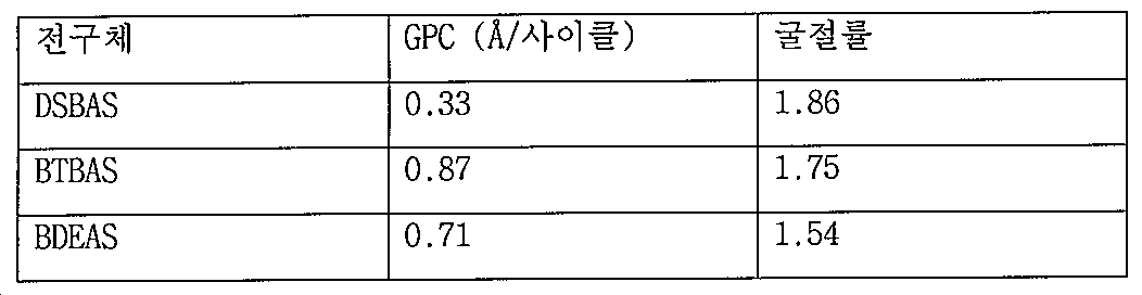
표 8을 참조로 하여, 모노아미노실란 전구체 DSBAS를 사용하여 증착된 막이 가장 높은 굴절률을 가졌는데, 이는 이러한 것이 보다 나은 질화규소 막임을 명시하는 것이다. 비스아미노실란들 중에서, BDEAS가 가장 낮은 굴절률, 즉 1.54를 가졌는데, 이는 보다 많은 산화규소 유사 막을 명시하는 것이다. 샘플들을 주변 대기에서 저장한 후에 이러한 막들의 굴절률을 다시 측정하였다. 도 2는, 막들의 굴절률이 산화로 인하여 시간에 따라 감소함을 나타낸다. 세 가지 막들 중에서, 모노아미노실란-증착 막 DSBAS 막은 비스아미노실란 증착 막 또는 BTBAS 또는 BDEAS 중 어느 하나 보다 더욱 높은 안정성을 갖는다. 비스아미노실란-증착 막들 중에서, BTBAS 막은 주변에서 대략 1일(~24 시간) 후에 1.75에서 1.57로 굴절률 감소를 나타내었다. 나머지 비스아미노실란-증착 막 또는 BDEAS는 훨씬 더 나쁜 안정성을 나타내었거나, 막 굴절률이 증착 직후에 1.57이다. 이러한 막들을 주변에서 150시간(7일) 동안 놓은 후에 XPS를 통해 조성에 대해 분석하였다. XPS 분석은 비스(아미노)실란-증착 막 또는 BDEAS 및 BTBAS 증착 막 둘 모두가 58% O, 6% C 및 3.5% N을 함유한 반면, 모노아미노실란-증착 막 또는 DSBAS 막이 2.5% O, 13.9% C 및 41% N을 함유함을 나타내었다. 이에 따라, DSBAS 증착 막은 BTBAS 또는 BDEAS 증착 막 중 어느 하나 보다 더욱 안정하였다.Referring to Table 8, the films deposited using the monoaminosilane precursor DSBAS had the highest refractive index, indicating that this is a better silicon nitride film. Of the bisaminosilanes, BDEAS had the lowest refractive index, 1.54, which specifies more silicon oxide-like films. After storing the samples in the ambient atmosphere, the refractive indices of these films were again measured. Figure 2 shows that the refractive index of the films decreases with time due to oxidation. Of the three films, the monoaminosilane-deposited film DSBAS film has a higher stability than either the bisaminosilane deposited film or either BTBAS or BDEAS. Of the bisaminosilane-deposited films, the BTBAS film exhibited a refractive index reduction from 1.75 to 1.57 after about 1 day (~ 24 hours) at the periphery. The remaining bisaminosilane-deposited film or BDEAS exhibited much worse stability, or the film index was 1.57 immediately after deposition. These membranes were placed for 150 hours (7 days) around and analyzed for composition via XPS. XPS analysis showed that both the bis (amino) silane-deposited film or the BDEAS and BTBAS deposited films contained 58% O, 6% C and 3.5% N, while the monoaminosilane- or DSBAS films contained 2.5% O, 13.9 % C and 41% N, respectively. Accordingly, the DSBAS deposited film was more stable than either of the BTBAS or BDEAS deposited films.
실시예 9. CN-1 샤워 헤드 타입 반응기를 이용하여 디-이소-프로필아미노실란(DIPAS)을 사용한 PEALD 질화규소 함유 막Example 9. PEALD silicon nitride-containing film using di-iso-propylaminosilane (DIPAS) using a CN-1 showerhead type reactor
규소 웨이퍼를 CN-1 PEALD 반응기에 로딩하고 2 torr의 챔버 압력과 함께 300℃로 가열하였다. DIPAS를 버블링법(bubbling method)을 이용하여 반응기로 전달하였다. ALD 사이클은 표 2에 제공되고 하기 공정 파라미터를 이용하는 공정 단계들로 이루어졌다:The silicon wafers were loaded into a CN-1 PEALD reactor and heated to 300 DEG C with a chamber pressure of 2 torr. DIPAS was transferred to the reactor using the bubbling method. The ALD cycle consisted of process steps provided in Table 2 and using the following process parameters:
1. 오가노아미노실란 전구체를 반응기에 도입1. Introduction of the organosiloxane precursor into the reactor
DIPAS: 전구체 용기를 관통하는 50 sccm 아르곤DIPAS: 50 sccm argon through the precursor vessel
아르곤 흐름: 100 sccmArgon flow: 100 sccm
Si 전구체 펄스: 1 초Si precursor pulse: 1 second
2. 불활성 가스 퍼징2. Inert Gas Purging
아르곤 및 질소의 전체 흐름 500 sccmTotal flow of argon and nitrogen 500 sccm
퍼지 시간: 10 초Purge time: 10 seconds
3. 플라즈마 온(plasma on)3. Plasma on
Ar 흐름: 0 내지 500 sccm Ar flow: 0 to 500 sccm
질소 흐름: 0 내지 500 sccmNitrogen flow: 0-500 sccm
Ar 및 질소의 전체 흐름: 500 sccmTotal flow of Ar and nitrogen: 500 sccm
플라즈마 출력: 125W (0.7 W/㎠)Plasma output: 125 W (0.7 W / cm 2)
플라즈마 시간: 5 초Plasma time: 5 seconds
4. 플라즈마 퍼징4. Plasma Purging
아르곤 및 질소의 전체 흐름: 500 sccmTotal flow of argon and nitrogen: 500 sccm
퍼지 시간: 10 초Purge time: 10 seconds
표 9는 공정 파라미터, 및 DIPAS를 사용하여 증착된 막들의 막 성질을 제공한다. 통상적인 DIPAS 막들은 1.2 내지 2.2%의 탄소 불순물을 갖는다.Table 9 provides process parameters and the film properties of the films deposited using DIPAS. Typical DIPAS films have 1.2 to 2.2% carbon impurities.
표 9. 공정 파라미터, 및 DIPAS를 사용하여 증착된 질화규소 함유 막들의 성질Table 9. Process parameters and properties of silicon nitride-containing films deposited using DIPAS

실시예 10. CN-1 샤워 헤드 타입 반응기에서 디-이소-프로필아미노실란(DIPAS)을 사용한 PEALD 규소 및 질소 함유 막Example 10. PEALD silicon and nitrogen containing membrane using di-iso-propylaminosilane (DIPAS) in a CN-1 showerhead type reactor
디-이소-프로필아미노실란(DIPAS) 및 He/N2 플라즈마로부터 규소 함유 막들을 증착하였다. 공정 파라미터 및 ALD 단계들은, Ar 가스 대신에 헬륨을 사용하는 것을 제외하고는 실시예 9에 기술된 것과 동일하였다. 표 10은 He/N2 플라즈마를 사용하여 증착된 막들 및 매우 낮은 묽은 HF 습윤 내에칭성(wet etch resistance; WER)을 나타낸다. 시험된 모든 He/N2 비에서, 막들은 WER >22.1 nm/분, 및 1.85 보다 더욱 낮은 굴절률을 갖는다.Silicon-containing films were deposited from di-iso-propylaminosilane (DIPAS) and He / N 2 plasma. The process parameters and ALD steps were the same as described in Example 9 except that helium was used instead of Ar gas. Table 10 shows films deposited using He / N 2 plasma and very low wet etch resistance (WER). At all He / N 2 ratios tested, the films have a WER > 22.1 nm / min, and a refractive index lower than 1.85.
표 10. 공정 파라미터, 및 DIPAS 및 He/N2 플라즈마로부터 증착된 질화규소 함유 막들의 막 성질Table 10. Process parameters and film properties of silicon nitride-containing films deposited from DIPAS and He / N 2 plasma

실시예 11. CN-1 샤워 헤드 타입 반응기에서 디-이소-프로필아미노실란(DIPAS)을 사용한 PEALD 질화규소 함유 막Example 11. PEALD silicon nitride-containing film using di-iso-propylaminosilane (DIPAS) in a CN-1 showerhead type reactor
하기 세부 공정 파라미터들과 함께 300℃ 및 2 torr의 챔버 압력에서 스크리닝(screening) PEALD 반응기를 이용하여 디-이소-프로필아미노실란(DIPAS) 및 단지 N2 플라즈마로부터 Si 함유 막들을 증착하였다:Si containing films were deposited from di-iso-propylaminosilane (DIPAS) and only N 2 plasma using a PEALD reactor screening at 300 ° C and a chamber pressure of 2 torr with the following detailed process parameters:
1. 유기아미노실란 전구체를 반응기에 도입: DIPAS1. Introduction of organosilane precursors into the reactor: DIPAS
전달 방법: 증기 인출(vapor draw)Delivery method: vapor draw
Si 전구체 펄스: 1 초Si precursor pulse: 1 second
N2 흐름: 500 sccm N 2 flow: 500 sccm
2. 불활성 가스 퍼징2. Inert Gas Purging
N2 흐름: 500 sccm N 2 flow: 500 sccm
퍼지 시간: 10 초Purge time: 10 seconds
3. 플라즈마 온3. Plasma on
질소 흐름: 500 sccm Nitrogen flow: 500 sccm
플라즈마 출력:125W (0.7 W/㎠)Plasma output: 125 W (0.7 W / cm 2)
플라즈마 시간: 5 초Plasma time: 5 seconds
4. 플라즈마 퍼징4. Plasma Purging
질소 흐름: 500 sccmNitrogen flow: 500 sccm
퍼지 시간: 10 초Purge time: 10 seconds
사이클 당 성장은 0.15 Å/사이클이며, 굴절률은 1.93이다.The growth rate per cycle is 0.15 A / cycle, and the refractive index is 1.93.
Claims (22)
a) 기판을 반응기에 제공하는 단계;
b) 반응기에 하기 화학식 (I), (II) 및 (III)으로 표현되는 하나 이상의 오가노아미노실란을 도입하는 단계로서, 하나 이상의 오가노아미노실란이 기판 표면의 일부 또는 전부 상에서 반응하여 화학흡착된 층(chemisorbed layer)을 제공하는 단계;
c) 반응기를 퍼지 가스(purge gas)로 퍼징하는 단계;
d) 질소 및 불활성 가스를 포함하는 플라즈마를 반응기에 도입하여 화학흡착된 층의 일부 또는 전부와 반응시키고 하나 이상의 반응성 사이트(reactive site)를 제공하는 단계로서, 플라즈마가 약 0.01 내지 약 1.5 W/㎠ 범위의 출력 밀도(power density)로 발생되는 단계; 및
e) 임의적으로, 반응기를 불활성 가스로 퍼징하는 단계를 포함하며,
질화규소 막의 요망되는 두께가 얻어질 때까지 단계 b) 내지 단계 e)가 반복되는, 방법:

상기 식에서, R1은 선형 또는 분지형 C3 내지 C10 알킬기, 선형 또는 분지형 C3 내지 C10 알케닐기, 선형 또는 분지형 C3 내지 C10 알키닐기, C1 내지 C6 디알킬아미노기, 전자 끄는 기, 및 C6 내지 C10 아릴기로부터 선택되며, R2는 수소, 선형 또는 분지형 C1 내지 C10 알킬기, 선형 또는 분지형 C3 내지 C6 알케닐기, 선형 또는 분지형 C3 내지 C6 알키닐기, C1 내지 C6 디알킬아미노기, C6 내지 C10 아릴기, 선형 또는 분지형 C1 내지 C6 플루오르화된 알킬기, 전자 끄는 기, 및 C4 내지 C10 아릴기로부터 선택되며, 임의적으로, R1 및 R2는 함께 연결되어 치환되거나 비치환된 방향족 고리 또는 치환되거나 비치환된 지방족 고리로부터 선택된 고리를 형성하며,
화학식 (III)에서, n은 1 또는 2이다.A method of forming a silicon nitride film on at least a surface of a substrate,
a) providing a substrate to a reactor;
b) introducing into the reactor at least one organosiloxane represented by the following formulas (I), (II) and (III), wherein at least one organoaminosilane reacts on some or all of the substrate surface to effect chemical adsorption Providing a chemisorbed layer;
c) purging the reactor with a purge gas;
d) introducing a plasma comprising nitrogen and an inert gas into the reactor to react with some or all of the chemisorbed layer and providing at least one reactive site, wherein the plasma has a plasma concentration in the range of from about 0.01 W / cm 2 to about 1.5 W / A power density of the range; And
e) optionally, purging the reactor with an inert gas,
Wherein step b) to step e) are repeated until the desired thickness of the silicon nitride film is obtained.
Wherein R 1 is a linear or branched C 3 to C 10 alkyl group, a linear or branched C 3 to C 10 alkenyl group, a linear or branched C 3 to C 10 alkynyl group, a C 1 to C 6 Dialkylamino group, is selected from electron-withdrawing group, and a C 6 to C 10 aryl group, R 2 is hydrogen, a linear or branched C 1 to C 10 alkyl group, a linear or branched C 3 to C 6 alkenyl group, a linear or Branched C 3 to C 6 alkynyl groups, C 1 to C 6 dialkylamino groups, C 6 to C 10 aryl groups, linear or branched C 1 to C 6 fluorinated alkyl groups, electron withdrawing groups, and C 4 to C 10 is selected from an aryl group, optionally, R 1 and R 2 are linked together with a substituted or unsubstituted aromatic ring or an unsubstituted or substituted form a ring selected from unsubstituted aliphatic ring, and
In formula (III), n is 1 or 2.
a) 기판을 반응기에 제공하는 단계;
b) 반응기에 디-이소-프로필아미노실란, 디-2차-부틸아미노실란, 페닐메틸아미노실란, 2,6-디메틸피페리디노실란, N-메틸사이클로헥실아미노실란, N-에틸사이클로헥실아미노실란, N-이소프로필사이클로헥실아미노실란, 2-메틸피페리디노실란, N-실릴데카하이드로퀴놀린, 2,2,6,6-테트라메틸피페리디노실란, 2-(N-실릴메틸아미노)피리딘, N-t-부틸디실라잔, N-t-펜틸디실라잔, N-(3-메틸-2-피리딜)디실라잔, N-(2-메틸페닐)디실라잔, N-(2-에틸페닐)디실라잔, N-(2,4,6-트리메틸페닐)디실라잔, N-(2,6-디-이소-프리필페닐)디실라잔, 디-이소-프로필아미노디실란, 디-이소-부틸아미노디실란, 디-2차-부틸아미노디실란, 2,6-디메틸피페리디노실란, N-메틸사이클로헥실아미노디실란, N-에틸사이클로헥실아미노디실란, 페닐메틸아미노디실란, 2-(N-디실릴메틸아미노)피리딘, N-페닐에틸디실란, N-이소프로필사이클로헥실아미노디실란, 1,1-(N,N'-디-3차-부틸에틸렌디아미노)디실란으로 이루어진 군으로부터 선택되는 하나 이상의 오가노아미노실란 전구체를 도입하는 단계로서, 하나 이상의 오가노아미노실란이 기판 표면의 일부 또는 전부 상에서 반응하여 화학흡착된 층을 제공하는 단계;
c) 반응기를 질소, 희가스 및 이들의 조합으로부터 선택된 하나 이상을 포함하는 퍼지 가스로 퍼징하는 단계;
d) 질소-함유 플라즈마를 반응기에 도입하여 화학흡착된 층의 일부 또는 전부와 반응하고 하나 이상의 반응성 사이트를 제공하는 단계로서, 플라즈마가 약 0.01 내지 약 1.5 W/㎠ 범위의 출력 밀도로 발생되는 단계; 및
e) 임의적으로, 반응기를 불활성 가스로 퍼징하는 단계를 포함하며,
질화규소 막의 요망되는 두께가 얻어질 때까지 단계 b) 내지 단계 e)가 반복되는 방법.A method of forming a silicon nitride film on at least a surface of a substrate,
a) providing a substrate to a reactor;
b) reacting in the reactor a di-iso-propylaminosilane, di-sec-butylaminosilane, phenylmethylaminosilane, 2,6-dimethylpiperidinosilane, N-methylcyclohexylaminosilane, N-ethylcyclohexylamino Silane, N-isopropylcyclohexylaminosilane, 2-methylpiperidinosilane, N-silyldecahydroquinoline, 2,2,6,6-tetramethylpiperidinosilane, 2- (N-silylmethylamino) (2-ethylphenyl) disilazane, N- (2-ethylphenyl) disilazane, N-methylpyridyl Di-iso-propylaminodisilane, di-iso-propylaminodisilane, di-iso-propylaminodisilane, N- (2,4,6-trimethylphenyl) disilazane, N- Butyldimethyldisilane, N-methylcyclohexylaminodisilane, N-ethylcyclohexylaminodisilane, phenylmethylaminodisilane, phenylmethylaminodiphenylsilane, N-methylcyclohexylaminodiphenylsilane, , 2- (N-disilylmethylamino) pyridine, N-phenyl Introducing at least one organosiloxane precursor selected from the group consisting of tributylsilane, tributylsilane, tributylsilane, tributylsilane, tributylsilane, tributylsilane, tributylsilane, tributylsilane, tributylsilane, Wherein at least one organosiloxane reacts on at least a portion of a substrate surface to provide a chemisorbed layer;
c) purging the reactor with a purge gas comprising at least one selected from nitrogen, noble gas and combinations thereof;
d) introducing a nitrogen-containing plasma into the reactor to react with some or all of the chemisorbed layer and providing at least one reactive site, wherein the plasma is generated at an output density in the range of about 0.01 to about 1.5 W / ; And
e) optionally, purging the reactor with an inert gas,
Wherein step b) to step e) are repeated until the desired thickness of the silicon nitride film is obtained.
a) 기판을 반응기에 제공하는 단계;
b) 반응기에 디-이소-프로필아미노실란, 디-2차-부틸아미노실란, 페닐메틸아미노실란, 2,6-디메틸피페리디노실란, N-메틸사이클로헥실아미노실란, N-에틸사이클로헥실아미노실란, N-이소프로필사이클로헥실아미노실란, 2-메틸피페리디노실란, N-실릴데카하이드로퀴놀린, 2,2,6,6-테트라메틸피페리디노실란, 2-(N-실릴메틸아미노)피리딘, N-t-부틸디실라잔, N-t-펜틸디실라잔, N-(3-메틸-2-피리딜)디실라잔, N-(2-메틸페닐)디실라잔, N-(2-에틸페닐)디실라잔, N-(2,4,6-트리메틸페닐)디실라잔, N-(2,6-디-이소-프리필페닐)디실라잔, 디-이소-프로필아미노디실란, 디-이소-부틸아미노디실란, 디-2차-부틸아미노디실란, 2,6-디메틸피페리디노실란, N-메틸사이클로헥실아미노디실란, N-에틸사이클로헥실아미노디실란, 페닐메틸아미노디실란, 2-(N-디실릴메틸아미노)피리딘, N-페닐에틸디실란, N-이소프로필사이클로헥실아미노디실란, 1,1-(N,N'-디-3차-부틸에틸렌디아미노)디실란으로 이루어진 군으로부터 선택된 하나 이상의 오가노아미노실란 전구체를 도입하는 단계로서, 하나 이상의 오가노아미노실란이 기판 표면의 일부 또는 전부 상에서 반응하여 화학흡착된 층을 제공하는 단계;
c) 반응기를 질소, 희가스 및 이들의 조합으로부터 선택된 하나 이상을 포함하는 퍼지 가스로 퍼징하는 단계;
d) 희가스를 포함하는 플라즈마를 반응기에 도입하여 화학흡착된 층의 일부 또는 전부와 반응하고 하나 이상의 반응성 사이트를 제공하는 단계로서, 플라즈마가 약 0.01 내지 약 1.5 W/㎠ 범위의 출력 밀도로 발생되는 단계; 및
e) 임의적으로, 반응기를 불활성 가스로 퍼징하는 단계를 포함하고,
질화규소 막의 요망되는 두께가 얻어질 때까지 단계 b) 내지 단계 e)가 반복되는 방법.A method of forming a silicon nitride film on at least a surface of a substrate,
a) providing a substrate to a reactor;
b) reacting in the reactor a di-iso-propylaminosilane, di-sec-butylaminosilane, phenylmethylaminosilane, 2,6-dimethylpiperidinosilane, N-methylcyclohexylaminosilane, N-ethylcyclohexylamino Silane, N-isopropylcyclohexylaminosilane, 2-methylpiperidinosilane, N-silyldecahydroquinoline, 2,2,6,6-tetramethylpiperidinosilane, 2- (N-silylmethylamino) (2-ethylphenyl) disilazane, N- (2-ethylphenyl) disilazane, N-methylpyridyl Di-iso-propylaminodisilane, di-iso-propylaminodisilane, di-iso-propylaminodisilane, N- (2,4,6-trimethylphenyl) disilazane, N- Butyldimethyldisilane, N-methylcyclohexylaminodisilane, N-ethylcyclohexylaminodisilane, phenylmethylaminodisilane, phenylmethylaminodiphenylsilane, N-methylcyclohexylaminodiphenylsilane, , 2- (N-disilylmethylamino) pyridine, N-phenyl Introducing at least one organoaminosilane precursor selected from the group consisting of tributyl silane, t-butyl silane, t-butyl silane, t-butyl silane, t-butyl silane, t-butyl silane, As a step, at least one organoaminosilane reacts on some or all of the substrate surface to provide a chemisorbed layer;
c) purging the reactor with a purge gas comprising at least one selected from nitrogen, noble gas and combinations thereof;
d) introducing a plasma comprising a noble gas into the reactor to react with some or all of the chemisorbed layer and providing at least one reactive site, wherein the plasma is generated at an output density in the range of about 0.01 to about 1.5 W / step; And
e) optionally, purging the reactor with an inert gas,
Wherein step b) to step e) are repeated until the desired thickness of the silicon nitride film is obtained.
Priority Applications (1)
| Application Number | Priority Date | Filing Date | Title |
|---|---|---|---|
| KR1020160150391A KR102256536B1 (en) | 2013-10-03 | 2016-11-11 | Methods for depositing silicon nitride films |
Applications Claiming Priority (4)
| Application Number | Priority Date | Filing Date | Title |
|---|---|---|---|
| US201361886406P | 2013-10-03 | 2013-10-03 | |
| US61/886,406 | 2013-10-03 | ||
| US14/498,044 US9905415B2 (en) | 2013-10-03 | 2014-09-26 | Methods for depositing silicon nitride films |
| US14/498,044 | 2014-09-26 |
Related Child Applications (1)
| Application Number | Title | Priority Date | Filing Date |
|---|---|---|---|
| KR1020160150391A Division KR102256536B1 (en) | 2013-10-03 | 2016-11-11 | Methods for depositing silicon nitride films |
Publications (1)
| Publication Number | Publication Date |
|---|---|
| KR20150040234A true KR20150040234A (en) | 2015-04-14 |
Family
ID=51663047
Family Applications (4)
| Application Number | Title | Priority Date | Filing Date |
|---|---|---|---|
| KR20140133394A KR20150040234A (en) | 2013-10-03 | 2014-10-02 | Methods for depositing silicon nitride films |
| KR1020160150391A KR102256536B1 (en) | 2013-10-03 | 2016-11-11 | Methods for depositing silicon nitride films |
| KR1020170018917A KR102281913B1 (en) | 2013-10-03 | 2017-02-10 | Methods for depositing silicon nitride films |
| KR1020210064384A KR102478568B1 (en) | 2013-10-03 | 2021-05-18 | Methods for depositing silicon nitride films |
Family Applications After (3)
| Application Number | Title | Priority Date | Filing Date |
|---|---|---|---|
| KR1020160150391A KR102256536B1 (en) | 2013-10-03 | 2016-11-11 | Methods for depositing silicon nitride films |
| KR1020170018917A KR102281913B1 (en) | 2013-10-03 | 2017-02-10 | Methods for depositing silicon nitride films |
| KR1020210064384A KR102478568B1 (en) | 2013-10-03 | 2021-05-18 | Methods for depositing silicon nitride films |
Country Status (6)
| Country | Link |
|---|---|
| US (1) | US9905415B2 (en) |
| EP (1) | EP2857552A3 (en) |
| JP (1) | JP6018149B2 (en) |
| KR (4) | KR20150040234A (en) |
| CN (1) | CN104831254B (en) |
| TW (1) | TWI565822B (en) |
Cited By (2)
| Publication number | Priority date | Publication date | Assignee | Title |
|---|---|---|---|---|
| KR20180034581A (en) * | 2015-07-31 | 2018-04-04 | 버슘머트리얼즈 유에스, 엘엘씨 | Compositions and methods for depositing silicon nitride films |
| KR20180053694A (en) * | 2015-09-11 | 2018-05-23 | 버슘머트리얼즈 유에스, 엘엘씨 | A method of depositing a conformal metal or metalloid silicon nitride film, |
Families Citing this family (227)
| Publication number | Priority date | Publication date | Assignee | Title |
|---|---|---|---|---|
| US20130023129A1 (en) | 2011-07-20 | 2013-01-24 | Asm America, Inc. | Pressure transmitter for a semiconductor processing environment |
| US10714315B2 (en) | 2012-10-12 | 2020-07-14 | Asm Ip Holdings B.V. | Semiconductor reaction chamber showerhead |
| US20160376700A1 (en) | 2013-02-01 | 2016-12-29 | Asm Ip Holding B.V. | System for treatment of deposition reactor |
| US10941490B2 (en) | 2014-10-07 | 2021-03-09 | Asm Ip Holding B.V. | Multiple temperature range susceptor, assembly, reactor and system including the susceptor, and methods of using the same |
| CN113025992B (en) * | 2014-10-24 | 2024-02-02 | 弗萨姆材料美国有限责任公司 | Composition and method for depositing silicon-containing film using the same |
| US10276355B2 (en) | 2015-03-12 | 2019-04-30 | Asm Ip Holding B.V. | Multi-zone reactor, system including the reactor, and method of using the same |
| US9748093B2 (en) * | 2015-03-18 | 2017-08-29 | Applied Materials, Inc. | Pulsed nitride encapsulation |
| US9646818B2 (en) * | 2015-03-23 | 2017-05-09 | Applied Materials, Inc. | Method of forming planar carbon layer by applying plasma power to a combination of hydrocarbon precursor and hydrogen-containing precursor |
| US10458018B2 (en) | 2015-06-26 | 2019-10-29 | Asm Ip Holding B.V. | Structures including metal carbide material, devices including the structures, and methods of forming same |
| US10745808B2 (en) * | 2015-07-24 | 2020-08-18 | Versum Materials Us, Llc | Methods for depositing Group 13 metal or metalloid nitride films |
| KR20170019668A (en) * | 2015-08-12 | 2017-02-22 | (주)디엔에프 | The manufacturing method of the silicon nitride film by using plasma enhanced atomic layer deposition |
| KR102153564B1 (en) * | 2015-10-06 | 2020-09-08 | 버슘머트리얼즈 유에스, 엘엘씨 | Method of depositing conformal metal or metalloid silicon nitride film |
| US10211308B2 (en) | 2015-10-21 | 2019-02-19 | Asm Ip Holding B.V. | NbMC layers |
| KR102458309B1 (en) | 2015-12-28 | 2022-10-24 | 삼성전자주식회사 | Method of forming a SiOCN material layer and method of fabricating a semiconductor device |
| US11139308B2 (en) | 2015-12-29 | 2021-10-05 | Asm Ip Holding B.V. | Atomic layer deposition of III-V compounds to form V-NAND devices |
| US10529554B2 (en) | 2016-02-19 | 2020-01-07 | Asm Ip Holding B.V. | Method for forming silicon nitride film selectively on sidewalls or flat surfaces of trenches |
| WO2017147150A1 (en) * | 2016-02-26 | 2017-08-31 | Versum Materials Us, Llc | Compositions and methods using same for deposition of silicon-containing film |
| EP3428959B1 (en) | 2016-03-11 | 2023-03-01 | Taiyo Nippon Sanso Corporation | Method for producing silicon nitride film, and silicon nitride film |
| US10319583B2 (en) * | 2016-03-13 | 2019-06-11 | Applied Materials, Inc. | Selective deposition of silicon nitride films for spacer applications |
| US10367080B2 (en) | 2016-05-02 | 2019-07-30 | Asm Ip Holding B.V. | Method of forming a germanium oxynitride film |
| US9859151B1 (en) | 2016-07-08 | 2018-01-02 | Asm Ip Holding B.V. | Selective film deposition method to form air gaps |
| US10612137B2 (en) | 2016-07-08 | 2020-04-07 | Asm Ip Holdings B.V. | Organic reactants for atomic layer deposition |
| US9929006B2 (en) * | 2016-07-20 | 2018-03-27 | Micron Technology, Inc. | Silicon chalcogenate precursors, methods of forming the silicon chalcogenate precursors, and related methods of forming silicon nitride and semiconductor structures |
| US9887082B1 (en) | 2016-07-28 | 2018-02-06 | Asm Ip Holding B.V. | Method and apparatus for filling a gap |
| US9812320B1 (en) | 2016-07-28 | 2017-11-07 | Asm Ip Holding B.V. | Method and apparatus for filling a gap |
| KR102532607B1 (en) | 2016-07-28 | 2023-05-15 | 에이에스엠 아이피 홀딩 비.브이. | Substrate processing apparatus and method of operating the same |
| KR102451069B1 (en) * | 2016-09-01 | 2022-10-05 | 에이에스엠 아이피 홀딩 비.브이. | Method for protecting layer by forming Hydrocarbon-based extremely thin film |
| US11532757B2 (en) | 2016-10-27 | 2022-12-20 | Asm Ip Holding B.V. | Deposition of charge trapping layers |
| US10714350B2 (en) | 2016-11-01 | 2020-07-14 | ASM IP Holdings, B.V. | Methods for forming a transition metal niobium nitride film on a substrate by atomic layer deposition and related semiconductor device structures |
| KR102546317B1 (en) | 2016-11-15 | 2023-06-21 | 에이에스엠 아이피 홀딩 비.브이. | Gas supply unit and substrate processing apparatus including the same |
| KR20180068582A (en) | 2016-12-14 | 2018-06-22 | 에이에스엠 아이피 홀딩 비.브이. | Substrate processing apparatus |
| US11447861B2 (en) | 2016-12-15 | 2022-09-20 | Asm Ip Holding B.V. | Sequential infiltration synthesis apparatus and a method of forming a patterned structure |
| US11581186B2 (en) | 2016-12-15 | 2023-02-14 | Asm Ip Holding B.V. | Sequential infiltration synthesis apparatus |
| US10269558B2 (en) | 2016-12-22 | 2019-04-23 | Asm Ip Holding B.V. | Method of forming a structure on a substrate |
| US11390950B2 (en) | 2017-01-10 | 2022-07-19 | Asm Ip Holding B.V. | Reactor system and method to reduce residue buildup during a film deposition process |
| US11017997B2 (en) * | 2017-01-13 | 2021-05-25 | Applied Materials, Inc. | Methods and apparatus for low temperature silicon nitride films |
| US10468261B2 (en) | 2017-02-15 | 2019-11-05 | Asm Ip Holding B.V. | Methods for forming a metallic film on a substrate by cyclical deposition and related semiconductor device structures |
| KR102105976B1 (en) * | 2017-03-29 | 2020-05-04 | (주)디엔에프 | Composition for depositing silicon-containing thin film and method for manufacturing silicon-containing thin film using the same |
| KR102093227B1 (en) * | 2017-04-20 | 2020-03-25 | (주)디엔에프 | Disilyl amine compound, method for preparing the same and composition for depositing silicon-containing thin film containing the same |
| US10770286B2 (en) | 2017-05-08 | 2020-09-08 | Asm Ip Holdings B.V. | Methods for selectively forming a silicon nitride film on a substrate and related semiconductor device structures |
| US11306395B2 (en) | 2017-06-28 | 2022-04-19 | Asm Ip Holding B.V. | Methods for depositing a transition metal nitride film on a substrate by atomic layer deposition and related deposition apparatus |
| TWI722292B (en) * | 2017-07-05 | 2021-03-21 | 美商應用材料股份有限公司 | Silicon nitride films with high nitrogen content |
| TWI762194B (en) | 2017-07-18 | 2022-04-21 | 美商應用材料股份有限公司 | Methods for depositing blocking layers on metal material surfaces |
| KR20190009245A (en) | 2017-07-18 | 2019-01-28 | 에이에스엠 아이피 홀딩 비.브이. | Methods for forming a semiconductor device structure and related semiconductor device structures |
| US11374112B2 (en) | 2017-07-19 | 2022-06-28 | Asm Ip Holding B.V. | Method for depositing a group IV semiconductor and related semiconductor device structures |
| US10590535B2 (en) | 2017-07-26 | 2020-03-17 | Asm Ip Holdings B.V. | Chemical treatment, deposition and/or infiltration apparatus and method for using the same |
| US10770336B2 (en) | 2017-08-08 | 2020-09-08 | Asm Ip Holding B.V. | Substrate lift mechanism and reactor including same |
| US10692741B2 (en) | 2017-08-08 | 2020-06-23 | Asm Ip Holdings B.V. | Radiation shield |
| US11769682B2 (en) | 2017-08-09 | 2023-09-26 | Asm Ip Holding B.V. | Storage apparatus for storing cassettes for substrates and processing apparatus equipped therewith |
| US11830730B2 (en) | 2017-08-29 | 2023-11-28 | Asm Ip Holding B.V. | Layer forming method and apparatus |
| US11295980B2 (en) | 2017-08-30 | 2022-04-05 | Asm Ip Holding B.V. | Methods for depositing a molybdenum metal film over a dielectric surface of a substrate by a cyclical deposition process and related semiconductor device structures |
| US11056344B2 (en) | 2017-08-30 | 2021-07-06 | Asm Ip Holding B.V. | Layer forming method |
| KR102491945B1 (en) | 2017-08-30 | 2023-01-26 | 에이에스엠 아이피 홀딩 비.브이. | Substrate processing apparatus |
| US10658205B2 (en) | 2017-09-28 | 2020-05-19 | Asm Ip Holdings B.V. | Chemical dispensing apparatus and methods for dispensing a chemical to a reaction chamber |
| US10403504B2 (en) | 2017-10-05 | 2019-09-03 | Asm Ip Holding B.V. | Method for selectively depositing a metallic film on a substrate |
| CN111316417B (en) | 2017-11-27 | 2023-12-22 | 阿斯莫Ip控股公司 | Storage device for storing wafer cassettes for use with batch ovens |
| TWI791689B (en) | 2017-11-27 | 2023-02-11 | 荷蘭商Asm智慧財產控股私人有限公司 | Apparatus including a clean mini environment |
| US10872771B2 (en) | 2018-01-16 | 2020-12-22 | Asm Ip Holding B. V. | Method for depositing a material film on a substrate within a reaction chamber by a cyclical deposition process and related device structures |
| KR20200108016A (en) | 2018-01-19 | 2020-09-16 | 에이에스엠 아이피 홀딩 비.브이. | Method of depositing a gap fill layer by plasma assisted deposition |
| TWI799494B (en) | 2018-01-19 | 2023-04-21 | 荷蘭商Asm 智慧財產控股公司 | Deposition method |
| US11081345B2 (en) | 2018-02-06 | 2021-08-03 | Asm Ip Holding B.V. | Method of post-deposition treatment for silicon oxide film |
| US10896820B2 (en) | 2018-02-14 | 2021-01-19 | Asm Ip Holding B.V. | Method for depositing a ruthenium-containing film on a substrate by a cyclical deposition process |
| EP3737779A1 (en) | 2018-02-14 | 2020-11-18 | ASM IP Holding B.V. | A method for depositing a ruthenium-containing film on a substrate by a cyclical deposition process |
| KR102636427B1 (en) | 2018-02-20 | 2024-02-13 | 에이에스엠 아이피 홀딩 비.브이. | Substrate processing method and apparatus |
| US10975470B2 (en) | 2018-02-23 | 2021-04-13 | Asm Ip Holding B.V. | Apparatus for detecting or monitoring for a chemical precursor in a high temperature environment |
| US11473195B2 (en) | 2018-03-01 | 2022-10-18 | Asm Ip Holding B.V. | Semiconductor processing apparatus and a method for processing a substrate |
| CN112005343A (en) | 2018-03-02 | 2020-11-27 | 朗姆研究公司 | Selective deposition using hydrolysis |
| US11629406B2 (en) | 2018-03-09 | 2023-04-18 | Asm Ip Holding B.V. | Semiconductor processing apparatus comprising one or more pyrometers for measuring a temperature of a substrate during transfer of the substrate |
| US11114283B2 (en) | 2018-03-16 | 2021-09-07 | Asm Ip Holding B.V. | Reactor, system including the reactor, and methods of manufacturing and using same |
| KR102646467B1 (en) | 2018-03-27 | 2024-03-11 | 에이에스엠 아이피 홀딩 비.브이. | Method of forming an electrode on a substrate and a semiconductor device structure including an electrode |
| US11230766B2 (en) | 2018-03-29 | 2022-01-25 | Asm Ip Holding B.V. | Substrate processing apparatus and method |
| KR20190128558A (en) | 2018-05-08 | 2019-11-18 | 에이에스엠 아이피 홀딩 비.브이. | Methods for depositing an oxide film on a substrate by a cyclical deposition process and related device structures |
| KR102596988B1 (en) | 2018-05-28 | 2023-10-31 | 에이에스엠 아이피 홀딩 비.브이. | Method of processing a substrate and a device manufactured by the same |
| US11718913B2 (en) | 2018-06-04 | 2023-08-08 | Asm Ip Holding B.V. | Gas distribution system and reactor system including same |
| US11270899B2 (en) | 2018-06-04 | 2022-03-08 | Asm Ip Holding B.V. | Wafer handling chamber with moisture reduction |
| US11286562B2 (en) | 2018-06-08 | 2022-03-29 | Asm Ip Holding B.V. | Gas-phase chemical reactor and method of using same |
| US10867839B2 (en) * | 2018-06-15 | 2020-12-15 | Taiwan Semiconductor Manufacturing Company, Ltd. | Patterning methods for semiconductor devices |
| KR102568797B1 (en) | 2018-06-21 | 2023-08-21 | 에이에스엠 아이피 홀딩 비.브이. | Substrate processing system |
| US10797133B2 (en) | 2018-06-21 | 2020-10-06 | Asm Ip Holding B.V. | Method for depositing a phosphorus doped silicon arsenide film and related semiconductor device structures |
| JP2021529254A (en) | 2018-06-27 | 2021-10-28 | エーエスエム・アイピー・ホールディング・ベー・フェー | Periodic deposition methods for forming metal-containing materials and films and structures containing metal-containing materials |
| WO2020003000A1 (en) | 2018-06-27 | 2020-01-02 | Asm Ip Holding B.V. | Cyclic deposition methods for forming metal-containing material and films and structures including the metal-containing material |
| US10612136B2 (en) | 2018-06-29 | 2020-04-07 | ASM IP Holding, B.V. | Temperature-controlled flange and reactor system including same |
| US10388513B1 (en) | 2018-07-03 | 2019-08-20 | Asm Ip Holding B.V. | Method for depositing silicon-free carbon-containing film as gap-fill layer by pulse plasma-assisted deposition |
| US10755922B2 (en) | 2018-07-03 | 2020-08-25 | Asm Ip Holding B.V. | Method for depositing silicon-free carbon-containing film as gap-fill layer by pulse plasma-assisted deposition |
| US20200058497A1 (en) * | 2018-08-20 | 2020-02-20 | Applied Materials, Inc | Silicon nitride forming precursor control |
| US11430674B2 (en) | 2018-08-22 | 2022-08-30 | Asm Ip Holding B.V. | Sensor array, apparatus for dispensing a vapor phase reactant to a reaction chamber and related methods |
| KR20200030162A (en) | 2018-09-11 | 2020-03-20 | 에이에스엠 아이피 홀딩 비.브이. | Method for deposition of a thin film |
| US11024523B2 (en) | 2018-09-11 | 2021-06-01 | Asm Ip Holding B.V. | Substrate processing apparatus and method |
| CN112805405B (en) * | 2018-09-24 | 2024-04-23 | 弗萨姆材料美国有限责任公司 | Method for producing silicon-and nitrogen-containing films |
| CN110970344A (en) | 2018-10-01 | 2020-04-07 | Asm Ip控股有限公司 | Substrate holding apparatus, system including the same, and method of using the same |
| US11232963B2 (en) | 2018-10-03 | 2022-01-25 | Asm Ip Holding B.V. | Substrate processing apparatus and method |
| KR102592699B1 (en) | 2018-10-08 | 2023-10-23 | 에이에스엠 아이피 홀딩 비.브이. | Substrate support unit and apparatuses for depositing thin film and processing the substrate including the same |
| US10847365B2 (en) * | 2018-10-11 | 2020-11-24 | Asm Ip Holding B.V. | Method of forming conformal silicon carbide film by cyclic CVD |
| KR102546322B1 (en) | 2018-10-19 | 2023-06-21 | 에이에스엠 아이피 홀딩 비.브이. | Substrate processing apparatus and substrate processing method |
| KR102605121B1 (en) | 2018-10-19 | 2023-11-23 | 에이에스엠 아이피 홀딩 비.브이. | Substrate processing apparatus and substrate processing method |
| US11087997B2 (en) | 2018-10-31 | 2021-08-10 | Asm Ip Holding B.V. | Substrate processing apparatus for processing substrates |
| KR20200051105A (en) | 2018-11-02 | 2020-05-13 | 에이에스엠 아이피 홀딩 비.브이. | Substrate support unit and substrate processing apparatus including the same |
| US11572620B2 (en) | 2018-11-06 | 2023-02-07 | Asm Ip Holding B.V. | Methods for selectively depositing an amorphous silicon film on a substrate |
| WO2020101437A1 (en) * | 2018-11-15 | 2020-05-22 | 주식회사 유피케미칼 | Silicon precursor compound, preparation method therefor, and silicon-containing film formation method using same |
| US10847366B2 (en) | 2018-11-16 | 2020-11-24 | Asm Ip Holding B.V. | Methods for depositing a transition metal chalcogenide film on a substrate by a cyclical deposition process |
| US10818758B2 (en) | 2018-11-16 | 2020-10-27 | Asm Ip Holding B.V. | Methods for forming a metal silicate film on a substrate in a reaction chamber and related semiconductor device structures |
| US11217444B2 (en) | 2018-11-30 | 2022-01-04 | Asm Ip Holding B.V. | Method for forming an ultraviolet radiation responsive metal oxide-containing film |
| KR102636428B1 (en) | 2018-12-04 | 2024-02-13 | 에이에스엠 아이피 홀딩 비.브이. | A method for cleaning a substrate processing apparatus |
| US11158513B2 (en) | 2018-12-13 | 2021-10-26 | Asm Ip Holding B.V. | Methods for forming a rhenium-containing film on a substrate by a cyclical deposition process and related semiconductor device structures |
| JP2020096183A (en) | 2018-12-14 | 2020-06-18 | エーエスエム・アイピー・ホールディング・ベー・フェー | Method of forming device structure using selective deposition of gallium nitride, and system for the same |
| TWI819180B (en) | 2019-01-17 | 2023-10-21 | 荷蘭商Asm 智慧財產控股公司 | Methods of forming a transition metal containing film on a substrate by a cyclical deposition process |
| KR20200091543A (en) | 2019-01-22 | 2020-07-31 | 에이에스엠 아이피 홀딩 비.브이. | Semiconductor processing device |
| CN113330141B (en) * | 2019-01-24 | 2023-10-17 | 应用材料公司 | Method for depositing silicon nitride |
| CN111524788B (en) | 2019-02-01 | 2023-11-24 | Asm Ip私人控股有限公司 | Method for topologically selective film formation of silicon oxide |
| US11482533B2 (en) | 2019-02-20 | 2022-10-25 | Asm Ip Holding B.V. | Apparatus and methods for plug fill deposition in 3-D NAND applications |
| KR102626263B1 (en) | 2019-02-20 | 2024-01-16 | 에이에스엠 아이피 홀딩 비.브이. | Cyclical deposition method including treatment step and apparatus for same |
| TW202104632A (en) | 2019-02-20 | 2021-02-01 | 荷蘭商Asm Ip私人控股有限公司 | Cyclical deposition method and apparatus for filling a recess formed within a substrate surface |
| TW202044325A (en) | 2019-02-20 | 2020-12-01 | 荷蘭商Asm Ip私人控股有限公司 | Method of filling a recess formed within a surface of a substrate, semiconductor structure formed according to the method, and semiconductor processing apparatus |
| TW202100794A (en) | 2019-02-22 | 2021-01-01 | 荷蘭商Asm Ip私人控股有限公司 | Substrate processing apparatus and method for processing substrate |
| US11742198B2 (en) | 2019-03-08 | 2023-08-29 | Asm Ip Holding B.V. | Structure including SiOCN layer and method of forming same |
| KR20200108242A (en) | 2019-03-08 | 2020-09-17 | 에이에스엠 아이피 홀딩 비.브이. | Method for Selective Deposition of Silicon Nitride Layer and Structure Including Selectively-Deposited Silicon Nitride Layer |
| KR20200108243A (en) | 2019-03-08 | 2020-09-17 | 에이에스엠 아이피 홀딩 비.브이. | Structure Including SiOC Layer and Method of Forming Same |
| KR20200116033A (en) | 2019-03-28 | 2020-10-08 | 에이에스엠 아이피 홀딩 비.브이. | Door opener and substrate processing apparatus provided therewith |
| KR20200116855A (en) | 2019-04-01 | 2020-10-13 | 에이에스엠 아이피 홀딩 비.브이. | Method of manufacturing semiconductor device |
| US11447864B2 (en) | 2019-04-19 | 2022-09-20 | Asm Ip Holding B.V. | Layer forming method and apparatus |
| KR20200125453A (en) | 2019-04-24 | 2020-11-04 | 에이에스엠 아이피 홀딩 비.브이. | Gas-phase reactor system and method of using same |
| KR20200130121A (en) | 2019-05-07 | 2020-11-18 | 에이에스엠 아이피 홀딩 비.브이. | Chemical source vessel with dip tube |
| KR20200130118A (en) | 2019-05-07 | 2020-11-18 | 에이에스엠 아이피 홀딩 비.브이. | Method for Reforming Amorphous Carbon Polymer Film |
| KR20200130652A (en) | 2019-05-10 | 2020-11-19 | 에이에스엠 아이피 홀딩 비.브이. | Method of depositing material onto a surface and structure formed according to the method |
| JP2020188255A (en) | 2019-05-16 | 2020-11-19 | エーエスエム アイピー ホールディング ビー.ブイ. | Wafer boat handling device, vertical batch furnace, and method |
| USD947913S1 (en) | 2019-05-17 | 2022-04-05 | Asm Ip Holding B.V. | Susceptor shaft |
| USD975665S1 (en) | 2019-05-17 | 2023-01-17 | Asm Ip Holding B.V. | Susceptor shaft |
| USD935572S1 (en) | 2019-05-24 | 2021-11-09 | Asm Ip Holding B.V. | Gas channel plate |
| KR20200141003A (en) | 2019-06-06 | 2020-12-17 | 에이에스엠 아이피 홀딩 비.브이. | Gas-phase reactor system including a gas detector |
| KR20200143254A (en) | 2019-06-11 | 2020-12-23 | 에이에스엠 아이피 홀딩 비.브이. | Method of forming an electronic structure using an reforming gas, system for performing the method, and structure formed using the method |
| USD944946S1 (en) | 2019-06-14 | 2022-03-01 | Asm Ip Holding B.V. | Shower plate |
| USD931978S1 (en) | 2019-06-27 | 2021-09-28 | Asm Ip Holding B.V. | Showerhead vacuum transport |
| KR20210005515A (en) | 2019-07-03 | 2021-01-14 | 에이에스엠 아이피 홀딩 비.브이. | Temperature control assembly for substrate processing apparatus and method of using same |
| JP2021015791A (en) | 2019-07-09 | 2021-02-12 | エーエスエム アイピー ホールディング ビー.ブイ. | Plasma device and substrate processing method using coaxial waveguide |
| CN112216646A (en) | 2019-07-10 | 2021-01-12 | Asm Ip私人控股有限公司 | Substrate supporting assembly and substrate processing device comprising same |
| KR20210010307A (en) | 2019-07-16 | 2021-01-27 | 에이에스엠 아이피 홀딩 비.브이. | Substrate processing apparatus |
| KR20210010816A (en) | 2019-07-17 | 2021-01-28 | 에이에스엠 아이피 홀딩 비.브이. | Radical assist ignition plasma system and method |
| KR20210010820A (en) | 2019-07-17 | 2021-01-28 | 에이에스엠 아이피 홀딩 비.브이. | Methods of forming silicon germanium structures |
| US11643724B2 (en) | 2019-07-18 | 2023-05-09 | Asm Ip Holding B.V. | Method of forming structures using a neutral beam |
| CN112242296A (en) | 2019-07-19 | 2021-01-19 | Asm Ip私人控股有限公司 | Method of forming topologically controlled amorphous carbon polymer films |
| CN112309843A (en) | 2019-07-29 | 2021-02-02 | Asm Ip私人控股有限公司 | Selective deposition method for achieving high dopant doping |
| CN112309899A (en) | 2019-07-30 | 2021-02-02 | Asm Ip私人控股有限公司 | Substrate processing apparatus |
| CN112309900A (en) | 2019-07-30 | 2021-02-02 | Asm Ip私人控股有限公司 | Substrate processing apparatus |
| US11227782B2 (en) | 2019-07-31 | 2022-01-18 | Asm Ip Holding B.V. | Vertical batch furnace assembly |
| US11587815B2 (en) | 2019-07-31 | 2023-02-21 | Asm Ip Holding B.V. | Vertical batch furnace assembly |
| US11587814B2 (en) | 2019-07-31 | 2023-02-21 | Asm Ip Holding B.V. | Vertical batch furnace assembly |
| CN112323048B (en) | 2019-08-05 | 2024-02-09 | Asm Ip私人控股有限公司 | Liquid level sensor for chemical source container |
| USD965524S1 (en) | 2019-08-19 | 2022-10-04 | Asm Ip Holding B.V. | Susceptor support |
| USD965044S1 (en) | 2019-08-19 | 2022-09-27 | Asm Ip Holding B.V. | Susceptor shaft |
| JP2021031769A (en) | 2019-08-21 | 2021-03-01 | エーエスエム アイピー ホールディング ビー.ブイ. | Production apparatus of mixed gas of film deposition raw material and film deposition apparatus |
| KR20210024423A (en) | 2019-08-22 | 2021-03-05 | 에이에스엠 아이피 홀딩 비.브이. | Method for forming a structure with a hole |
| USD930782S1 (en) | 2019-08-22 | 2021-09-14 | Asm Ip Holding B.V. | Gas distributor |
| USD940837S1 (en) | 2019-08-22 | 2022-01-11 | Asm Ip Holding B.V. | Electrode |
| USD979506S1 (en) | 2019-08-22 | 2023-02-28 | Asm Ip Holding B.V. | Insulator |
| USD949319S1 (en) | 2019-08-22 | 2022-04-19 | Asm Ip Holding B.V. | Exhaust duct |
| US11286558B2 (en) | 2019-08-23 | 2022-03-29 | Asm Ip Holding B.V. | Methods for depositing a molybdenum nitride film on a surface of a substrate by a cyclical deposition process and related semiconductor device structures including a molybdenum nitride film |
| KR20210024420A (en) | 2019-08-23 | 2021-03-05 | 에이에스엠 아이피 홀딩 비.브이. | Method for depositing silicon oxide film having improved quality by peald using bis(diethylamino)silane |
| KR20210029090A (en) | 2019-09-04 | 2021-03-15 | 에이에스엠 아이피 홀딩 비.브이. | Methods for selective deposition using a sacrificial capping layer |
| KR20210029663A (en) | 2019-09-05 | 2021-03-16 | 에이에스엠 아이피 홀딩 비.브이. | Substrate processing apparatus |
| US11562901B2 (en) | 2019-09-25 | 2023-01-24 | Asm Ip Holding B.V. | Substrate processing method |
| CN112593212B (en) | 2019-10-02 | 2023-12-22 | Asm Ip私人控股有限公司 | Method for forming topologically selective silicon oxide film by cyclic plasma enhanced deposition process |
| TW202129060A (en) | 2019-10-08 | 2021-08-01 | 荷蘭商Asm Ip控股公司 | Substrate processing device, and substrate processing method |
| TW202115273A (en) | 2019-10-10 | 2021-04-16 | 荷蘭商Asm Ip私人控股有限公司 | Method of forming a photoresist underlayer and structure including same |
| KR20210045930A (en) | 2019-10-16 | 2021-04-27 | 에이에스엠 아이피 홀딩 비.브이. | Method of Topology-Selective Film Formation of Silicon Oxide |
| US11637014B2 (en) | 2019-10-17 | 2023-04-25 | Asm Ip Holding B.V. | Methods for selective deposition of doped semiconductor material |
| KR20210047808A (en) | 2019-10-21 | 2021-04-30 | 에이에스엠 아이피 홀딩 비.브이. | Apparatus and methods for selectively etching films |
| US11646205B2 (en) | 2019-10-29 | 2023-05-09 | Asm Ip Holding B.V. | Methods of selectively forming n-type doped material on a surface, systems for selectively forming n-type doped material, and structures formed using same |
| KR20210054983A (en) | 2019-11-05 | 2021-05-14 | 에이에스엠 아이피 홀딩 비.브이. | Structures with doped semiconductor layers and methods and systems for forming same |
| US11501968B2 (en) | 2019-11-15 | 2022-11-15 | Asm Ip Holding B.V. | Method for providing a semiconductor device with silicon filled gaps |
| KR20210062561A (en) | 2019-11-20 | 2021-05-31 | 에이에스엠 아이피 홀딩 비.브이. | Method of depositing carbon-containing material on a surface of a substrate, structure formed using the method, and system for forming the structure |
| KR20210065848A (en) | 2019-11-26 | 2021-06-04 | 에이에스엠 아이피 홀딩 비.브이. | Methods for selectivley forming a target film on a substrate comprising a first dielectric surface and a second metallic surface |
| CN112951697A (en) | 2019-11-26 | 2021-06-11 | Asm Ip私人控股有限公司 | Substrate processing apparatus |
| CN112885693A (en) | 2019-11-29 | 2021-06-01 | Asm Ip私人控股有限公司 | Substrate processing apparatus |
| CN112885692A (en) | 2019-11-29 | 2021-06-01 | Asm Ip私人控股有限公司 | Substrate processing apparatus |
| JP2021090042A (en) | 2019-12-02 | 2021-06-10 | エーエスエム アイピー ホールディング ビー.ブイ. | Substrate processing apparatus and substrate processing method |
| KR20210070898A (en) | 2019-12-04 | 2021-06-15 | 에이에스엠 아이피 홀딩 비.브이. | Substrate processing apparatus |
| CN112992667A (en) | 2019-12-17 | 2021-06-18 | Asm Ip私人控股有限公司 | Method of forming vanadium nitride layer and structure including vanadium nitride layer |
| KR20210080214A (en) | 2019-12-19 | 2021-06-30 | 에이에스엠 아이피 홀딩 비.브이. | Methods for filling a gap feature on a substrate and related semiconductor structures |
| TW202140135A (en) | 2020-01-06 | 2021-11-01 | 荷蘭商Asm Ip私人控股有限公司 | Gas supply assembly and valve plate assembly |
| KR20210095050A (en) | 2020-01-20 | 2021-07-30 | 에이에스엠 아이피 홀딩 비.브이. | Method of forming thin film and method of modifying surface of thin film |
| TW202130846A (en) | 2020-02-03 | 2021-08-16 | 荷蘭商Asm Ip私人控股有限公司 | Method of forming structures including a vanadium or indium layer |
| TW202146882A (en) | 2020-02-04 | 2021-12-16 | 荷蘭商Asm Ip私人控股有限公司 | Method of verifying an article, apparatus for verifying an article, and system for verifying a reaction chamber |
| US11776846B2 (en) | 2020-02-07 | 2023-10-03 | Asm Ip Holding B.V. | Methods for depositing gap filling fluids and related systems and devices |
| US11781243B2 (en) | 2020-02-17 | 2023-10-10 | Asm Ip Holding B.V. | Method for depositing low temperature phosphorous-doped silicon |
| KR20210116240A (en) | 2020-03-11 | 2021-09-27 | 에이에스엠 아이피 홀딩 비.브이. | Substrate handling device with adjustable joints |
| US11876356B2 (en) | 2020-03-11 | 2024-01-16 | Asm Ip Holding B.V. | Lockout tagout assembly and system and method of using same |
| KR20210117157A (en) | 2020-03-12 | 2021-09-28 | 에이에스엠 아이피 홀딩 비.브이. | Method for Fabricating Layer Structure Having Target Topological Profile |
| KR20210124042A (en) | 2020-04-02 | 2021-10-14 | 에이에스엠 아이피 홀딩 비.브이. | Thin film forming method |
| TW202146689A (en) | 2020-04-03 | 2021-12-16 | 荷蘭商Asm Ip控股公司 | Method for forming barrier layer and method for manufacturing semiconductor device |
| TW202145344A (en) | 2020-04-08 | 2021-12-01 | 荷蘭商Asm Ip私人控股有限公司 | Apparatus and methods for selectively etching silcon oxide films |
| US11821078B2 (en) | 2020-04-15 | 2023-11-21 | Asm Ip Holding B.V. | Method for forming precoat film and method for forming silicon-containing film |
| KR20210132576A (en) | 2020-04-24 | 2021-11-04 | 에이에스엠 아이피 홀딩 비.브이. | Method of forming vanadium nitride-containing layer and structure comprising the same |
| KR20210132600A (en) | 2020-04-24 | 2021-11-04 | 에이에스엠 아이피 홀딩 비.브이. | Methods and systems for depositing a layer comprising vanadium, nitrogen, and a further element |
| KR20210132605A (en) | 2020-04-24 | 2021-11-04 | 에이에스엠 아이피 홀딩 비.브이. | Vertical batch furnace assembly comprising a cooling gas supply |
| KR20210134226A (en) | 2020-04-29 | 2021-11-09 | 에이에스엠 아이피 홀딩 비.브이. | Solid source precursor vessel |
| KR20210134869A (en) | 2020-05-01 | 2021-11-11 | 에이에스엠 아이피 홀딩 비.브이. | Fast FOUP swapping with a FOUP handler |
| KR20210141379A (en) | 2020-05-13 | 2021-11-23 | 에이에스엠 아이피 홀딩 비.브이. | Laser alignment fixture for a reactor system |
| TW202147383A (en) | 2020-05-19 | 2021-12-16 | 荷蘭商Asm Ip私人控股有限公司 | Substrate processing apparatus |
| KR20210145078A (en) | 2020-05-21 | 2021-12-01 | 에이에스엠 아이피 홀딩 비.브이. | Structures including multiple carbon layers and methods of forming and using same |
| TW202201602A (en) | 2020-05-29 | 2022-01-01 | 荷蘭商Asm Ip私人控股有限公司 | Substrate processing device |
| US11965239B2 (en) * | 2020-06-17 | 2024-04-23 | Entegris, Inc. | Method for nucleation of conductive nitride films |
| TW202218133A (en) | 2020-06-24 | 2022-05-01 | 荷蘭商Asm Ip私人控股有限公司 | Method for forming a layer provided with silicon |
| TW202217953A (en) | 2020-06-30 | 2022-05-01 | 荷蘭商Asm Ip私人控股有限公司 | Substrate processing method |
| KR20220010438A (en) | 2020-07-17 | 2022-01-25 | 에이에스엠 아이피 홀딩 비.브이. | Structures and methods for use in photolithography |
| TW202204662A (en) | 2020-07-20 | 2022-02-01 | 荷蘭商Asm Ip私人控股有限公司 | Method and system for depositing molybdenum layers |
| CN111883543B (en) * | 2020-07-28 | 2022-09-27 | 北海惠科光电技术有限公司 | Manufacturing method of array substrate, array substrate and display device |
| TW202212623A (en) | 2020-08-26 | 2022-04-01 | 荷蘭商Asm Ip私人控股有限公司 | Method of forming metal silicon oxide layer and metal silicon oxynitride layer, semiconductor structure, and system |
| USD990534S1 (en) | 2020-09-11 | 2023-06-27 | Asm Ip Holding B.V. | Weighted lift pin |
| USD1012873S1 (en) | 2020-09-24 | 2024-01-30 | Asm Ip Holding B.V. | Electrode for semiconductor processing apparatus |
| US11979171B2 (en) | 2020-10-13 | 2024-05-07 | Microchip Technology Incorporated | Reduced complexity encoders and related systems, methods, and devices |
| TW202229613A (en) | 2020-10-14 | 2022-08-01 | 荷蘭商Asm Ip私人控股有限公司 | Method of depositing material on stepped structure |
| KR20220053482A (en) | 2020-10-22 | 2022-04-29 | 에이에스엠 아이피 홀딩 비.브이. | Method of depositing vanadium metal, structure, device and a deposition assembly |
| TW202223136A (en) | 2020-10-28 | 2022-06-16 | 荷蘭商Asm Ip私人控股有限公司 | Method for forming layer on substrate, and semiconductor processing system |
| KR20220076343A (en) | 2020-11-30 | 2022-06-08 | 에이에스엠 아이피 홀딩 비.브이. | an injector configured for arrangement within a reaction chamber of a substrate processing apparatus |
| US11946137B2 (en) | 2020-12-16 | 2024-04-02 | Asm Ip Holding B.V. | Runout and wobble measurement fixtures |
| TW202231903A (en) | 2020-12-22 | 2022-08-16 | 荷蘭商Asm Ip私人控股有限公司 | Transition metal deposition method, transition metal layer, and deposition assembly for depositing transition metal on substrate |
| US11658025B2 (en) | 2021-01-18 | 2023-05-23 | Applied Materials, Inc. | Chalcogen precursors for deposition of silicon nitride |
| US11551926B2 (en) | 2021-01-22 | 2023-01-10 | Micron Technology, Inc. | Methods of forming a microelectronic device, and related systems and additional methods |
| USD980813S1 (en) | 2021-05-11 | 2023-03-14 | Asm Ip Holding B.V. | Gas flow control plate for substrate processing apparatus |
| USD980814S1 (en) | 2021-05-11 | 2023-03-14 | Asm Ip Holding B.V. | Gas distributor for substrate processing apparatus |
| USD981973S1 (en) | 2021-05-11 | 2023-03-28 | Asm Ip Holding B.V. | Reactor wall for substrate processing apparatus |
| USD1023959S1 (en) | 2021-05-11 | 2024-04-23 | Asm Ip Holding B.V. | Electrode for substrate processing apparatus |
| TWI809454B (en) * | 2021-07-19 | 2023-07-21 | 南亞科技股份有限公司 | Method of manufacturing semiconductor structure |
| USD990441S1 (en) | 2021-09-07 | 2023-06-27 | Asm Ip Holding B.V. | Gas flow control plate |
| US20230126516A1 (en) * | 2021-10-27 | 2023-04-27 | Asm Ip Holding B.V. | Methods and systems for forming doped silicon nitride films |
| KR102638053B1 (en) | 2021-11-15 | 2024-02-16 | 이지운 | A buoy having a function of maintaining buoyancy in case of breakage and a method for manufacturing the same |
| CN114836730B (en) * | 2021-12-30 | 2024-01-02 | 长江存储科技有限责任公司 | Atomic layer deposition method of oxide film |
Family Cites Families (25)
| Publication number | Priority date | Publication date | Assignee | Title |
|---|---|---|---|---|
| US5803975A (en) * | 1996-03-01 | 1998-09-08 | Canon Kabushiki Kaisha | Microwave plasma processing apparatus and method therefor |
| US6528430B2 (en) | 2001-05-01 | 2003-03-04 | Samsung Electronics Co., Ltd. | Method of forming silicon containing thin films by atomic layer deposition utilizing Si2C16 and NH3 |
| US6391803B1 (en) | 2001-06-20 | 2002-05-21 | Samsung Electronics Co., Ltd. | Method of forming silicon containing thin films by atomic layer deposition utilizing trisdimethylaminosilane |
| JP3937892B2 (en) | 2002-04-01 | 2007-06-27 | 日本電気株式会社 | Thin film forming method and semiconductor device manufacturing method |
| CN101572232B (en) * | 2002-12-20 | 2011-12-21 | 应用材料有限公司 | A method for forming a high quality low temperature silicon nitride layer |
| US20050227017A1 (en) * | 2003-10-31 | 2005-10-13 | Yoshihide Senzaki | Low temperature deposition of silicon nitride |
| US7875312B2 (en) * | 2006-05-23 | 2011-01-25 | Air Products And Chemicals, Inc. | Process for producing silicon oxide films for organoaminosilane precursors |
| US8530361B2 (en) * | 2006-05-23 | 2013-09-10 | Air Products And Chemicals, Inc. | Process for producing silicon and oxide films from organoaminosilane precursors |
| US7678422B2 (en) * | 2006-12-13 | 2010-03-16 | Air Products And Chemicals, Inc. | Cyclic chemical vapor deposition of metal-silicon containing films |
| KR100821082B1 (en) * | 2006-12-15 | 2008-04-08 | 동부일렉트로닉스 주식회사 | The fabricating method of semiconductor device |
| US7651961B2 (en) | 2007-03-30 | 2010-01-26 | Tokyo Electron Limited | Method for forming strained silicon nitride films and a device containing such films |
| WO2009039251A1 (en) | 2007-09-18 | 2009-03-26 | L'air Liquide - Societe Anonyme Pour L'etude Et L'exploitation Des Procedes Georges Claude | Method of forming silicon-containing films |
| US20090155606A1 (en) | 2007-12-13 | 2009-06-18 | Asm Genitech Korea Ltd. | Methods of depositing a silicon nitride film |
| US20100081293A1 (en) | 2008-10-01 | 2010-04-01 | Applied Materials, Inc. | Methods for forming silicon nitride based film or silicon carbon based film |
| US8912353B2 (en) | 2010-06-02 | 2014-12-16 | Air Products And Chemicals, Inc. | Organoaminosilane precursors and methods for depositing films comprising same |
| JP5625624B2 (en) | 2010-08-27 | 2014-11-19 | 東京エレクトロン株式会社 | Film forming apparatus, film forming method, and storage medium |
| US8465811B2 (en) | 2011-01-28 | 2013-06-18 | Asm Japan K.K. | Method of depositing film by atomic layer deposition with pulse-time-modulated plasma |
| US8771807B2 (en) * | 2011-05-24 | 2014-07-08 | Air Products And Chemicals, Inc. | Organoaminosilane precursors and methods for making and using same |
| KR20160093093A (en) | 2011-06-03 | 2016-08-05 | 에어 프로덕츠 앤드 케미칼스, 인코오포레이티드 | Compositions and processes for depositing carbon-doped silicon-containing films |
| US8993072B2 (en) | 2011-09-27 | 2015-03-31 | Air Products And Chemicals, Inc. | Halogenated organoaminosilane precursors and methods for depositing films comprising same |
| US8586487B2 (en) | 2012-01-18 | 2013-11-19 | Applied Materials, Inc. | Low temperature plasma enhanced chemical vapor deposition of conformal silicon carbon nitride and silicon nitride films |
| US9337018B2 (en) * | 2012-06-01 | 2016-05-10 | Air Products And Chemicals, Inc. | Methods for depositing films with organoaminodisilane precursors |
| US9978585B2 (en) * | 2012-06-01 | 2018-05-22 | Versum Materials Us, Llc | Organoaminodisilane precursors and methods for depositing films comprising same |
| US10573511B2 (en) * | 2013-03-13 | 2020-02-25 | Asm Ip Holding B.V. | Methods for forming silicon nitride thin films |
| US9796739B2 (en) * | 2013-06-26 | 2017-10-24 | Versum Materials Us, Llc | AZA-polysilane precursors and methods for depositing films comprising same |
-
2014
- 2014-09-26 US US14/498,044 patent/US9905415B2/en active Active
- 2014-10-01 TW TW103134304A patent/TWI565822B/en active
- 2014-10-02 KR KR20140133394A patent/KR20150040234A/en active Application Filing
- 2014-10-03 EP EP14187603.7A patent/EP2857552A3/en active Pending
- 2014-10-03 JP JP2014204854A patent/JP6018149B2/en active Active
- 2014-10-08 CN CN201410857912.0A patent/CN104831254B/en active Active
-
2016
- 2016-11-11 KR KR1020160150391A patent/KR102256536B1/en active IP Right Grant
-
2017
- 2017-02-10 KR KR1020170018917A patent/KR102281913B1/en active IP Right Grant
-
2021
- 2021-05-18 KR KR1020210064384A patent/KR102478568B1/en active IP Right Grant
Cited By (2)
| Publication number | Priority date | Publication date | Assignee | Title |
|---|---|---|---|---|
| KR20180034581A (en) * | 2015-07-31 | 2018-04-04 | 버슘머트리얼즈 유에스, 엘엘씨 | Compositions and methods for depositing silicon nitride films |
| KR20180053694A (en) * | 2015-09-11 | 2018-05-23 | 버슘머트리얼즈 유에스, 엘엘씨 | A method of depositing a conformal metal or metalloid silicon nitride film, |
Also Published As
| Publication number | Publication date |
|---|---|
| JP2015073099A (en) | 2015-04-16 |
| CN104831254A (en) | 2015-08-12 |
| EP2857552A3 (en) | 2015-09-23 |
| KR102256536B1 (en) | 2021-05-25 |
| KR20210060412A (en) | 2021-05-26 |
| KR102478568B1 (en) | 2022-12-15 |
| US9905415B2 (en) | 2018-02-27 |
| KR102281913B1 (en) | 2021-07-23 |
| CN104831254B (en) | 2019-04-12 |
| TWI565822B (en) | 2017-01-11 |
| KR20160132804A (en) | 2016-11-21 |
| TW201514332A (en) | 2015-04-16 |
| JP6018149B2 (en) | 2016-11-02 |
| US20150099375A1 (en) | 2015-04-09 |
| EP2857552A2 (en) | 2015-04-08 |
| KR20170018872A (en) | 2017-02-20 |
Similar Documents
| Publication | Publication Date | Title |
|---|---|---|
| KR102478568B1 (en) | Methods for depositing silicon nitride films | |
| US11035039B2 (en) | Compositions and methods for depositing silicon nitride films | |
| JP7025534B2 (en) | Compositions and Methods for Silicon-Containing Membrane Deposits | |
| US10242864B2 (en) | High temperature atomic layer deposition of silicon oxide thin films | |
| EP2860182B1 (en) | Organoaminosilane precursors and methods for depositing films comprising same | |
| US9447287B2 (en) | Compositions and processes for depositing carbon-doped silicon-containing films | |
| US11049714B2 (en) | Silyl substituted organoamines as precursors for high growth rate silicon-containing films | |
| TW202035430A (en) | Compositions and methods using same for silicon containing films |
Legal Events
| Date | Code | Title | Description |
|---|---|---|---|
| A201 | Request for examination | ||
| E902 | Notification of reason for refusal | ||
| AMND | Amendment | ||
| E601 | Decision to refuse application | ||
| AMND | Amendment | ||
| A107 | Divisional application of patent | ||
| J201 | Request for trial against refusal decision | ||
| N231 | Notification of change of applicant | ||
| J301 | Trial decision |
Free format text: TRIAL NUMBER: 2016101006443; TRIAL DECISION FOR APPEAL AGAINST DECISION TO DECLINE REFUSAL REQUESTED 20161111 Effective date: 20181018 |