KR20150002500A - Semiconductor device - Google Patents
Semiconductor device Download PDFInfo
- Publication number
- KR20150002500A KR20150002500A KR20140078066A KR20140078066A KR20150002500A KR 20150002500 A KR20150002500 A KR 20150002500A KR 20140078066 A KR20140078066 A KR 20140078066A KR 20140078066 A KR20140078066 A KR 20140078066A KR 20150002500 A KR20150002500 A KR 20150002500A
- Authority
- KR
- South Korea
- Prior art keywords
- layer
- oxide semiconductor
- transistor
- electrode layer
- insulating layer
- Prior art date
Links
- 239000004065 semiconductor Substances 0.000 title claims abstract description 418
- 239000013078 crystal Substances 0.000 claims abstract description 46
- 238000010894 electron beam technology Methods 0.000 claims description 85
- 239000000523 sample Substances 0.000 claims description 53
- 238000000034 method Methods 0.000 claims description 52
- 229910052738 indium Inorganic materials 0.000 claims description 28
- APFVFJFRJDLVQX-UHFFFAOYSA-N indium atom Chemical compound [In] APFVFJFRJDLVQX-UHFFFAOYSA-N 0.000 claims description 27
- 229910052782 aluminium Inorganic materials 0.000 claims description 18
- 229910052733 gallium Inorganic materials 0.000 claims description 14
- 229910052726 zirconium Inorganic materials 0.000 claims description 14
- 229910052684 Cerium Inorganic materials 0.000 claims description 13
- 229910052746 lanthanum Inorganic materials 0.000 claims description 13
- 229910052718 tin Inorganic materials 0.000 claims description 13
- 230000007547 defect Effects 0.000 abstract description 21
- 238000009413 insulation Methods 0.000 abstract description 6
- 230000004888 barrier function Effects 0.000 abstract description 5
- 238000003475 lamination Methods 0.000 abstract description 3
- 239000010410 layer Substances 0.000 description 953
- 239000000758 substrate Substances 0.000 description 60
- 229910052760 oxygen Inorganic materials 0.000 description 53
- QVGXLLKOCUKJST-UHFFFAOYSA-N atomic oxygen Chemical compound [O] QVGXLLKOCUKJST-UHFFFAOYSA-N 0.000 description 48
- 239000001301 oxygen Substances 0.000 description 48
- 239000011701 zinc Substances 0.000 description 42
- 239000000463 material Substances 0.000 description 28
- 238000010586 diagram Methods 0.000 description 23
- 238000010438 heat treatment Methods 0.000 description 23
- 239000003990 capacitor Substances 0.000 description 22
- VYPSYNLAJGMNEJ-UHFFFAOYSA-N Silicium dioxide Chemical compound O=[Si]=O VYPSYNLAJGMNEJ-UHFFFAOYSA-N 0.000 description 21
- 239000004973 liquid crystal related substance Substances 0.000 description 21
- 230000006870 function Effects 0.000 description 19
- IJGRMHOSHXDMSA-UHFFFAOYSA-N Atomic nitrogen Chemical compound N#N IJGRMHOSHXDMSA-UHFFFAOYSA-N 0.000 description 18
- 206010021143 Hypoxia Diseases 0.000 description 17
- 239000002159 nanocrystal Substances 0.000 description 17
- 125000004429 atom Chemical group 0.000 description 16
- 239000001257 hydrogen Substances 0.000 description 16
- 229910052739 hydrogen Inorganic materials 0.000 description 16
- 229910052581 Si3N4 Inorganic materials 0.000 description 15
- XUIMIQQOPSSXEZ-UHFFFAOYSA-N Silicon Chemical compound [Si] XUIMIQQOPSSXEZ-UHFFFAOYSA-N 0.000 description 15
- 239000012535 impurity Substances 0.000 description 15
- 229910052710 silicon Inorganic materials 0.000 description 15
- 239000010703 silicon Substances 0.000 description 15
- HQVNEWCFYHHQES-UHFFFAOYSA-N silicon nitride Chemical compound N12[Si]34N5[Si]62N3[Si]51N64 HQVNEWCFYHHQES-UHFFFAOYSA-N 0.000 description 15
- 229910052725 zinc Inorganic materials 0.000 description 15
- 239000012298 atmosphere Substances 0.000 description 14
- 238000004519 manufacturing process Methods 0.000 description 14
- 239000000470 constituent Substances 0.000 description 13
- 150000004767 nitrides Chemical class 0.000 description 12
- UFHFLCQGNIYNRP-UHFFFAOYSA-N Hydrogen Chemical compound [H][H] UFHFLCQGNIYNRP-UHFFFAOYSA-N 0.000 description 11
- 229910052719 titanium Inorganic materials 0.000 description 11
- 239000010936 titanium Substances 0.000 description 11
- 238000005259 measurement Methods 0.000 description 10
- 239000000203 mixture Substances 0.000 description 10
- 230000008569 process Effects 0.000 description 10
- 239000007789 gas Substances 0.000 description 9
- 229910052757 nitrogen Inorganic materials 0.000 description 9
- 238000004544 sputter deposition Methods 0.000 description 9
- HCHKCACWOHOZIP-UHFFFAOYSA-N Zinc Chemical compound [Zn] HCHKCACWOHOZIP-UHFFFAOYSA-N 0.000 description 8
- 229910052751 metal Inorganic materials 0.000 description 8
- 239000002184 metal Substances 0.000 description 8
- 229910052814 silicon oxide Inorganic materials 0.000 description 8
- RTAQQCXQSZGOHL-UHFFFAOYSA-N Titanium Chemical compound [Ti] RTAQQCXQSZGOHL-UHFFFAOYSA-N 0.000 description 7
- 238000002441 X-ray diffraction Methods 0.000 description 7
- PMHQVHHXPFUNSP-UHFFFAOYSA-M copper(1+);methylsulfanylmethane;bromide Chemical compound Br[Cu].CSC PMHQVHHXPFUNSP-UHFFFAOYSA-M 0.000 description 7
- 238000000151 deposition Methods 0.000 description 7
- TWNQGVIAIRXVLR-UHFFFAOYSA-N oxo(oxoalumanyloxy)alumane Chemical compound O=[Al]O[Al]=O TWNQGVIAIRXVLR-UHFFFAOYSA-N 0.000 description 7
- XLYOFNOQVPJJNP-UHFFFAOYSA-N water Substances O XLYOFNOQVPJJNP-UHFFFAOYSA-N 0.000 description 7
- 229910001868 water Inorganic materials 0.000 description 7
- XAGFODPZIPBFFR-UHFFFAOYSA-N aluminium Chemical compound [Al] XAGFODPZIPBFFR-UHFFFAOYSA-N 0.000 description 6
- 238000004891 communication Methods 0.000 description 6
- 230000008021 deposition Effects 0.000 description 6
- 230000005669 field effect Effects 0.000 description 6
- 150000002431 hydrogen Chemical class 0.000 description 6
- 230000001678 irradiating effect Effects 0.000 description 6
- RYGMFSIKBFXOCR-UHFFFAOYSA-N Copper Chemical compound [Cu] RYGMFSIKBFXOCR-UHFFFAOYSA-N 0.000 description 5
- 238000004458 analytical method Methods 0.000 description 5
- 229910052802 copper Inorganic materials 0.000 description 5
- 239000010949 copper Substances 0.000 description 5
- 238000009792 diffusion process Methods 0.000 description 5
- 229910052732 germanium Inorganic materials 0.000 description 5
- 229910052735 hafnium Inorganic materials 0.000 description 5
- 229910044991 metal oxide Inorganic materials 0.000 description 5
- 150000004706 metal oxides Chemical class 0.000 description 5
- SIWVEOZUMHYXCS-UHFFFAOYSA-N oxo(oxoyttriooxy)yttrium Chemical compound O=[Y]O[Y]=O SIWVEOZUMHYXCS-UHFFFAOYSA-N 0.000 description 5
- 230000002093 peripheral effect Effects 0.000 description 5
- 238000012545 processing Methods 0.000 description 5
- 229910052727 yttrium Inorganic materials 0.000 description 5
- 238000003917 TEM image Methods 0.000 description 4
- XLOMVQKBTHCTTD-UHFFFAOYSA-N Zinc monoxide Chemical compound [Zn]=O XLOMVQKBTHCTTD-UHFFFAOYSA-N 0.000 description 4
- -1 argon ions Chemical class 0.000 description 4
- 230000015572 biosynthetic process Effects 0.000 description 4
- 230000000903 blocking effect Effects 0.000 description 4
- AJNVQOSZGJRYEI-UHFFFAOYSA-N digallium;oxygen(2-) Chemical compound [O-2].[O-2].[O-2].[Ga+3].[Ga+3] AJNVQOSZGJRYEI-UHFFFAOYSA-N 0.000 description 4
- 238000005530 etching Methods 0.000 description 4
- 229910001195 gallium oxide Inorganic materials 0.000 description 4
- 229910000449 hafnium oxide Inorganic materials 0.000 description 4
- WIHZLLGSGQNAGK-UHFFFAOYSA-N hafnium(4+);oxygen(2-) Chemical compound [O-2].[O-2].[Hf+4] WIHZLLGSGQNAGK-UHFFFAOYSA-N 0.000 description 4
- 229910003437 indium oxide Inorganic materials 0.000 description 4
- PJXISJQVUVHSOJ-UHFFFAOYSA-N indium(iii) oxide Chemical compound [O-2].[O-2].[O-2].[In+3].[In+3] PJXISJQVUVHSOJ-UHFFFAOYSA-N 0.000 description 4
- 239000011261 inert gas Substances 0.000 description 4
- 230000001590 oxidative effect Effects 0.000 description 4
- 239000002356 single layer Substances 0.000 description 4
- 238000000992 sputter etching Methods 0.000 description 4
- 238000003860 storage Methods 0.000 description 4
- 229910052721 tungsten Inorganic materials 0.000 description 4
- 239000010937 tungsten Substances 0.000 description 4
- OKTJSMMVPCPJKN-UHFFFAOYSA-N Carbon Chemical compound [C] OKTJSMMVPCPJKN-UHFFFAOYSA-N 0.000 description 3
- XKRFYHLGVUSROY-UHFFFAOYSA-N argon Substances [Ar] XKRFYHLGVUSROY-UHFFFAOYSA-N 0.000 description 3
- GPBUGPUPKAGMDK-UHFFFAOYSA-N azanylidynemolybdenum Chemical compound [Mo]#N GPBUGPUPKAGMDK-UHFFFAOYSA-N 0.000 description 3
- 229910052799 carbon Inorganic materials 0.000 description 3
- 230000001413 cellular effect Effects 0.000 description 3
- 150000001875 compounds Chemical class 0.000 description 3
- 150000002500 ions Chemical class 0.000 description 3
- 239000011159 matrix material Substances 0.000 description 3
- QGLKJKCYBOYXKC-UHFFFAOYSA-N nonaoxidotritungsten Chemical compound O=[W]1(=O)O[W](=O)(=O)O[W](=O)(=O)O1 QGLKJKCYBOYXKC-UHFFFAOYSA-N 0.000 description 3
- 150000002894 organic compounds Chemical class 0.000 description 3
- 238000001228 spectrum Methods 0.000 description 3
- 239000000126 substance Substances 0.000 description 3
- WFKWXMTUELFFGS-UHFFFAOYSA-N tungsten Chemical compound [W] WFKWXMTUELFFGS-UHFFFAOYSA-N 0.000 description 3
- 229910001930 tungsten oxide Inorganic materials 0.000 description 3
- 238000001039 wet etching Methods 0.000 description 3
- VYZAMTAEIAYCRO-UHFFFAOYSA-N Chromium Chemical compound [Cr] VYZAMTAEIAYCRO-UHFFFAOYSA-N 0.000 description 2
- 208000005156 Dehydration Diseases 0.000 description 2
- ZOKXTWBITQBERF-UHFFFAOYSA-N Molybdenum Chemical compound [Mo] ZOKXTWBITQBERF-UHFFFAOYSA-N 0.000 description 2
- 229910052779 Neodymium Inorganic materials 0.000 description 2
- PXHVJJICTQNCMI-UHFFFAOYSA-N Nickel Chemical compound [Ni] PXHVJJICTQNCMI-UHFFFAOYSA-N 0.000 description 2
- MWUXSHHQAYIFBG-UHFFFAOYSA-N Nitric oxide Chemical compound O=[N] MWUXSHHQAYIFBG-UHFFFAOYSA-N 0.000 description 2
- BPQQTUXANYXVAA-UHFFFAOYSA-N Orthosilicate Chemical compound [O-][Si]([O-])([O-])[O-] BPQQTUXANYXVAA-UHFFFAOYSA-N 0.000 description 2
- 229910000577 Silicon-germanium Inorganic materials 0.000 description 2
- GWEVSGVZZGPLCZ-UHFFFAOYSA-N Titan oxide Chemical compound O=[Ti]=O GWEVSGVZZGPLCZ-UHFFFAOYSA-N 0.000 description 2
- NRTOMJZYCJJWKI-UHFFFAOYSA-N Titanium nitride Chemical compound [Ti]#N NRTOMJZYCJJWKI-UHFFFAOYSA-N 0.000 description 2
- LEVVHYCKPQWKOP-UHFFFAOYSA-N [Si].[Ge] Chemical compound [Si].[Ge] LEVVHYCKPQWKOP-UHFFFAOYSA-N 0.000 description 2
- 229910052783 alkali metal Inorganic materials 0.000 description 2
- 150000001340 alkali metals Chemical class 0.000 description 2
- 229910052784 alkaline earth metal Inorganic materials 0.000 description 2
- 150000001342 alkaline earth metals Chemical class 0.000 description 2
- 239000000956 alloy Substances 0.000 description 2
- 229910052786 argon Inorganic materials 0.000 description 2
- 238000003491 array Methods 0.000 description 2
- 238000004380 ashing Methods 0.000 description 2
- 238000000231 atomic layer deposition Methods 0.000 description 2
- 230000015556 catabolic process Effects 0.000 description 2
- 239000000919 ceramic Substances 0.000 description 2
- 229910052804 chromium Inorganic materials 0.000 description 2
- 239000011651 chromium Substances 0.000 description 2
- 239000004020 conductor Substances 0.000 description 2
- 230000018044 dehydration Effects 0.000 description 2
- 238000006297 dehydration reaction Methods 0.000 description 2
- 238000006356 dehydrogenation reaction Methods 0.000 description 2
- 238000001312 dry etching Methods 0.000 description 2
- 230000000694 effects Effects 0.000 description 2
- 230000005281 excited state Effects 0.000 description 2
- 239000011521 glass Substances 0.000 description 2
- VBJZVLUMGGDVMO-UHFFFAOYSA-N hafnium atom Chemical compound [Hf] VBJZVLUMGGDVMO-UHFFFAOYSA-N 0.000 description 2
- AMGQUBHHOARCQH-UHFFFAOYSA-N indium;oxotin Chemical compound [In].[Sn]=O AMGQUBHHOARCQH-UHFFFAOYSA-N 0.000 description 2
- 238000005468 ion implantation Methods 0.000 description 2
- MRELNEQAGSRDBK-UHFFFAOYSA-N lanthanum(3+);oxygen(2-) Chemical compound [O-2].[O-2].[O-2].[La+3].[La+3] MRELNEQAGSRDBK-UHFFFAOYSA-N 0.000 description 2
- 238000001451 molecular beam epitaxy Methods 0.000 description 2
- 229910052750 molybdenum Inorganic materials 0.000 description 2
- 239000011733 molybdenum Substances 0.000 description 2
- PLDDOISOJJCEMH-UHFFFAOYSA-N neodymium(3+);oxygen(2-) Chemical compound [O-2].[O-2].[O-2].[Nd+3].[Nd+3] PLDDOISOJJCEMH-UHFFFAOYSA-N 0.000 description 2
- 238000005498 polishing Methods 0.000 description 2
- 239000010453 quartz Substances 0.000 description 2
- 230000006798 recombination Effects 0.000 description 2
- HBMJWWWQQXIZIP-UHFFFAOYSA-N silicon carbide Chemical compound [Si+]#[C-] HBMJWWWQQXIZIP-UHFFFAOYSA-N 0.000 description 2
- 229910010271 silicon carbide Inorganic materials 0.000 description 2
- 229910052715 tantalum Inorganic materials 0.000 description 2
- GUVRBAGPIYLISA-UHFFFAOYSA-N tantalum atom Chemical compound [Ta] GUVRBAGPIYLISA-UHFFFAOYSA-N 0.000 description 2
- OGIDPMRJRNCKJF-UHFFFAOYSA-N titanium oxide Inorganic materials [Ti]=O OGIDPMRJRNCKJF-UHFFFAOYSA-N 0.000 description 2
- 238000012546 transfer Methods 0.000 description 2
- 239000011787 zinc oxide Substances 0.000 description 2
- 229910000838 Al alloy Inorganic materials 0.000 description 1
- JBRZTFJDHDCESZ-UHFFFAOYSA-N AsGa Chemical compound [As]#[Ga] JBRZTFJDHDCESZ-UHFFFAOYSA-N 0.000 description 1
- ZOXJGFHDIHLPTG-UHFFFAOYSA-N Boron Chemical compound [B] ZOXJGFHDIHLPTG-UHFFFAOYSA-N 0.000 description 1
- MYMOFIZGZYHOMD-UHFFFAOYSA-N Dioxygen Chemical compound O=O MYMOFIZGZYHOMD-UHFFFAOYSA-N 0.000 description 1
- GYHNNYVSQQEPJS-UHFFFAOYSA-N Gallium Chemical compound [Ga] GYHNNYVSQQEPJS-UHFFFAOYSA-N 0.000 description 1
- 229910001218 Gallium arsenide Inorganic materials 0.000 description 1
- 229910004129 HfSiO Inorganic materials 0.000 description 1
- 108010083687 Ion Pumps Proteins 0.000 description 1
- OAICVXFJPJFONN-UHFFFAOYSA-N Phosphorus Chemical compound [P] OAICVXFJPJFONN-UHFFFAOYSA-N 0.000 description 1
- BQCADISMDOOEFD-UHFFFAOYSA-N Silver Chemical compound [Ag] BQCADISMDOOEFD-UHFFFAOYSA-N 0.000 description 1
- QCWXUUIWCKQGHC-UHFFFAOYSA-N Zirconium Chemical compound [Zr] QCWXUUIWCKQGHC-UHFFFAOYSA-N 0.000 description 1
- 230000009471 action Effects 0.000 description 1
- 229910045601 alloy Inorganic materials 0.000 description 1
- 239000012300 argon atmosphere Substances 0.000 description 1
- NWAIGJYBQQYSPW-UHFFFAOYSA-N azanylidyneindigane Chemical compound [In]#N NWAIGJYBQQYSPW-UHFFFAOYSA-N 0.000 description 1
- 239000002585 base Substances 0.000 description 1
- 230000005540 biological transmission Effects 0.000 description 1
- 229910052796 boron Inorganic materials 0.000 description 1
- 150000001721 carbon Chemical group 0.000 description 1
- 239000002041 carbon nanotube Substances 0.000 description 1
- 229910021393 carbon nanotube Inorganic materials 0.000 description 1
- 239000000969 carrier Substances 0.000 description 1
- 229910000420 cerium oxide Inorganic materials 0.000 description 1
- 230000008859 change Effects 0.000 description 1
- 238000005229 chemical vapour deposition Methods 0.000 description 1
- 238000011109 contamination Methods 0.000 description 1
- 238000005520 cutting process Methods 0.000 description 1
- 229910001882 dioxygen Inorganic materials 0.000 description 1
- 238000007599 discharging Methods 0.000 description 1
- 230000005684 electric field Effects 0.000 description 1
- GNPVGFCGXDBREM-UHFFFAOYSA-N germanium atom Chemical compound [Ge] GNPVGFCGXDBREM-UHFFFAOYSA-N 0.000 description 1
- 230000005283 ground state Effects 0.000 description 1
- 125000005843 halogen group Chemical group 0.000 description 1
- 230000012447 hatching Effects 0.000 description 1
- MYMOFIZGZYHOMD-UHFFFAOYSA-O hydridodioxygen(1+) Chemical compound [OH+]=O MYMOFIZGZYHOMD-UHFFFAOYSA-O 0.000 description 1
- 125000004435 hydrogen atom Chemical group [H]* 0.000 description 1
- 238000007654 immersion Methods 0.000 description 1
- 238000003780 insertion Methods 0.000 description 1
- 230000037431 insertion Effects 0.000 description 1
- 230000010354 integration Effects 0.000 description 1
- 239000011229 interlayer Substances 0.000 description 1
- 230000007774 longterm Effects 0.000 description 1
- CPLXHLVBOLITMK-UHFFFAOYSA-N magnesium oxide Inorganic materials [Mg]=O CPLXHLVBOLITMK-UHFFFAOYSA-N 0.000 description 1
- 239000000395 magnesium oxide Substances 0.000 description 1
- AXZKOIWUVFPNLO-UHFFFAOYSA-N magnesium;oxygen(2-) Chemical compound [O-2].[Mg+2] AXZKOIWUVFPNLO-UHFFFAOYSA-N 0.000 description 1
- 238000012423 maintenance Methods 0.000 description 1
- 230000007246 mechanism Effects 0.000 description 1
- 239000007769 metal material Substances 0.000 description 1
- 230000004048 modification Effects 0.000 description 1
- 238000012986 modification Methods 0.000 description 1
- 229910021421 monocrystalline silicon Inorganic materials 0.000 description 1
- QEFYFXOXNSNQGX-UHFFFAOYSA-N neodymium atom Chemical compound [Nd] QEFYFXOXNSNQGX-UHFFFAOYSA-N 0.000 description 1
- 229910052759 nickel Inorganic materials 0.000 description 1
- RUFLMLWJRZAWLJ-UHFFFAOYSA-N nickel silicide Chemical compound [Ni]=[Si]=[Ni] RUFLMLWJRZAWLJ-UHFFFAOYSA-N 0.000 description 1
- 229910021334 nickel silicide Inorganic materials 0.000 description 1
- 239000012299 nitrogen atmosphere Substances 0.000 description 1
- BMMGVYCKOGBVEV-UHFFFAOYSA-N oxo(oxoceriooxy)cerium Chemical compound [Ce]=O.O=[Ce]=O BMMGVYCKOGBVEV-UHFFFAOYSA-N 0.000 description 1
- BPUBBGLMJRNUCC-UHFFFAOYSA-N oxygen(2-);tantalum(5+) Chemical compound [O-2].[O-2].[O-2].[O-2].[O-2].[Ta+5].[Ta+5] BPUBBGLMJRNUCC-UHFFFAOYSA-N 0.000 description 1
- RVTZCBVAJQQJTK-UHFFFAOYSA-N oxygen(2-);zirconium(4+) Chemical compound [O-2].[O-2].[Zr+4] RVTZCBVAJQQJTK-UHFFFAOYSA-N 0.000 description 1
- 230000003071 parasitic effect Effects 0.000 description 1
- 230000000737 periodic effect Effects 0.000 description 1
- 229910052698 phosphorus Inorganic materials 0.000 description 1
- 239000011574 phosphorus Substances 0.000 description 1
- 230000000704 physical effect Effects 0.000 description 1
- 238000009832 plasma treatment Methods 0.000 description 1
- 229910021420 polycrystalline silicon Inorganic materials 0.000 description 1
- 229920005591 polysilicon Polymers 0.000 description 1
- 238000005215 recombination Methods 0.000 description 1
- 230000003252 repetitive effect Effects 0.000 description 1
- 229910052594 sapphire Inorganic materials 0.000 description 1
- 239000010980 sapphire Substances 0.000 description 1
- 229910052706 scandium Inorganic materials 0.000 description 1
- SIXSYDAISGFNSX-UHFFFAOYSA-N scandium atom Chemical compound [Sc] SIXSYDAISGFNSX-UHFFFAOYSA-N 0.000 description 1
- 238000001004 secondary ion mass spectrometry Methods 0.000 description 1
- 238000000926 separation method Methods 0.000 description 1
- 229910021332 silicide Inorganic materials 0.000 description 1
- FVBUAEGBCNSCDD-UHFFFAOYSA-N silicide(4-) Chemical compound [Si-4] FVBUAEGBCNSCDD-UHFFFAOYSA-N 0.000 description 1
- 229910052709 silver Inorganic materials 0.000 description 1
- 239000004332 silver Substances 0.000 description 1
- 238000009751 slip forming Methods 0.000 description 1
- 238000001179 sorption measurement Methods 0.000 description 1
- 238000005477 sputtering target Methods 0.000 description 1
- 238000000859 sublimation Methods 0.000 description 1
- 230000008022 sublimation Effects 0.000 description 1
- MZLGASXMSKOWSE-UHFFFAOYSA-N tantalum nitride Chemical compound [Ta]#N MZLGASXMSKOWSE-UHFFFAOYSA-N 0.000 description 1
- 229910001936 tantalum oxide Inorganic materials 0.000 description 1
- XOLBLPGZBRYERU-UHFFFAOYSA-N tin dioxide Chemical compound O=[Sn]=O XOLBLPGZBRYERU-UHFFFAOYSA-N 0.000 description 1
- 229910001887 tin oxide Inorganic materials 0.000 description 1
- 238000002834 transmittance Methods 0.000 description 1
- 229910052720 vanadium Inorganic materials 0.000 description 1
- VWQVUPCCIRVNHF-UHFFFAOYSA-N yttrium atom Chemical compound [Y] VWQVUPCCIRVNHF-UHFFFAOYSA-N 0.000 description 1
- AKJVMGQSGCSQBU-UHFFFAOYSA-N zinc azanidylidenezinc Chemical compound [Zn++].[N-]=[Zn].[N-]=[Zn] AKJVMGQSGCSQBU-UHFFFAOYSA-N 0.000 description 1
- YVTHLONGBIQYBO-UHFFFAOYSA-N zinc indium(3+) oxygen(2-) Chemical compound [O--].[Zn++].[In+3] YVTHLONGBIQYBO-UHFFFAOYSA-N 0.000 description 1
- 229910001928 zirconium oxide Inorganic materials 0.000 description 1
Images


Classifications
-
- H—ELECTRICITY
- H01—ELECTRIC ELEMENTS
- H01L—SEMICONDUCTOR DEVICES NOT COVERED BY CLASS H10
- H01L29/00—Semiconductor devices adapted for rectifying, amplifying, oscillating or switching, or capacitors or resistors with at least one potential-jump barrier or surface barrier, e.g. PN junction depletion layer or carrier concentration layer; Details of semiconductor bodies or of electrodes thereof ; Multistep manufacturing processes therefor
- H01L29/66—Types of semiconductor device ; Multistep manufacturing processes therefor
- H01L29/68—Types of semiconductor device ; Multistep manufacturing processes therefor controllable by only the electric current supplied, or only the electric potential applied, to an electrode which does not carry the current to be rectified, amplified or switched
- H01L29/76—Unipolar devices, e.g. field effect transistors
- H01L29/772—Field effect transistors
- H01L29/78—Field effect transistors with field effect produced by an insulated gate
- H01L29/786—Thin film transistors, i.e. transistors with a channel being at least partly a thin film
- H01L29/7869—Thin film transistors, i.e. transistors with a channel being at least partly a thin film having a semiconductor body comprising an oxide semiconductor material, e.g. zinc oxide, copper aluminium oxide, cadmium stannate
-
- H—ELECTRICITY
- H01—ELECTRIC ELEMENTS
- H01L—SEMICONDUCTOR DEVICES NOT COVERED BY CLASS H10
- H01L27/00—Devices consisting of a plurality of semiconductor or other solid-state components formed in or on a common substrate
- H01L27/02—Devices consisting of a plurality of semiconductor or other solid-state components formed in or on a common substrate including semiconductor components specially adapted for rectifying, oscillating, amplifying or switching and having at least one potential-jump barrier or surface barrier; including integrated passive circuit elements with at least one potential-jump barrier or surface barrier
- H01L27/12—Devices consisting of a plurality of semiconductor or other solid-state components formed in or on a common substrate including semiconductor components specially adapted for rectifying, oscillating, amplifying or switching and having at least one potential-jump barrier or surface barrier; including integrated passive circuit elements with at least one potential-jump barrier or surface barrier the substrate being other than a semiconductor body, e.g. an insulating body
- H01L27/1214—Devices consisting of a plurality of semiconductor or other solid-state components formed in or on a common substrate including semiconductor components specially adapted for rectifying, oscillating, amplifying or switching and having at least one potential-jump barrier or surface barrier; including integrated passive circuit elements with at least one potential-jump barrier or surface barrier the substrate being other than a semiconductor body, e.g. an insulating body comprising a plurality of TFTs formed on a non-semiconducting substrate, e.g. driving circuits for AMLCDs
- H01L27/1222—Devices consisting of a plurality of semiconductor or other solid-state components formed in or on a common substrate including semiconductor components specially adapted for rectifying, oscillating, amplifying or switching and having at least one potential-jump barrier or surface barrier; including integrated passive circuit elements with at least one potential-jump barrier or surface barrier the substrate being other than a semiconductor body, e.g. an insulating body comprising a plurality of TFTs formed on a non-semiconducting substrate, e.g. driving circuits for AMLCDs with a particular composition, shape or crystalline structure of the active layer
- H01L27/1225—Devices consisting of a plurality of semiconductor or other solid-state components formed in or on a common substrate including semiconductor components specially adapted for rectifying, oscillating, amplifying or switching and having at least one potential-jump barrier or surface barrier; including integrated passive circuit elements with at least one potential-jump barrier or surface barrier the substrate being other than a semiconductor body, e.g. an insulating body comprising a plurality of TFTs formed on a non-semiconducting substrate, e.g. driving circuits for AMLCDs with a particular composition, shape or crystalline structure of the active layer with semiconductor materials not belonging to the group IV of the periodic table, e.g. InGaZnO
-
- H—ELECTRICITY
- H01—ELECTRIC ELEMENTS
- H01L—SEMICONDUCTOR DEVICES NOT COVERED BY CLASS H10
- H01L27/00—Devices consisting of a plurality of semiconductor or other solid-state components formed in or on a common substrate
- H01L27/02—Devices consisting of a plurality of semiconductor or other solid-state components formed in or on a common substrate including semiconductor components specially adapted for rectifying, oscillating, amplifying or switching and having at least one potential-jump barrier or surface barrier; including integrated passive circuit elements with at least one potential-jump barrier or surface barrier
- H01L27/12—Devices consisting of a plurality of semiconductor or other solid-state components formed in or on a common substrate including semiconductor components specially adapted for rectifying, oscillating, amplifying or switching and having at least one potential-jump barrier or surface barrier; including integrated passive circuit elements with at least one potential-jump barrier or surface barrier the substrate being other than a semiconductor body, e.g. an insulating body
- H01L27/1214—Devices consisting of a plurality of semiconductor or other solid-state components formed in or on a common substrate including semiconductor components specially adapted for rectifying, oscillating, amplifying or switching and having at least one potential-jump barrier or surface barrier; including integrated passive circuit elements with at least one potential-jump barrier or surface barrier the substrate being other than a semiconductor body, e.g. an insulating body comprising a plurality of TFTs formed on a non-semiconducting substrate, e.g. driving circuits for AMLCDs
- H01L27/1259—Multistep manufacturing methods
- H01L27/127—Multistep manufacturing methods with a particular formation, treatment or patterning of the active layer specially adapted to the circuit arrangement
-
- H—ELECTRICITY
- H01—ELECTRIC ELEMENTS
- H01L—SEMICONDUCTOR DEVICES NOT COVERED BY CLASS H10
- H01L29/00—Semiconductor devices adapted for rectifying, amplifying, oscillating or switching, or capacitors or resistors with at least one potential-jump barrier or surface barrier, e.g. PN junction depletion layer or carrier concentration layer; Details of semiconductor bodies or of electrodes thereof ; Multistep manufacturing processes therefor
- H01L29/02—Semiconductor bodies ; Multistep manufacturing processes therefor
- H01L29/04—Semiconductor bodies ; Multistep manufacturing processes therefor characterised by their crystalline structure, e.g. polycrystalline, cubic or particular orientation of crystalline planes
-
- H—ELECTRICITY
- H01—ELECTRIC ELEMENTS
- H01L—SEMICONDUCTOR DEVICES NOT COVERED BY CLASS H10
- H01L29/00—Semiconductor devices adapted for rectifying, amplifying, oscillating or switching, or capacitors or resistors with at least one potential-jump barrier or surface barrier, e.g. PN junction depletion layer or carrier concentration layer; Details of semiconductor bodies or of electrodes thereof ; Multistep manufacturing processes therefor
- H01L29/02—Semiconductor bodies ; Multistep manufacturing processes therefor
- H01L29/06—Semiconductor bodies ; Multistep manufacturing processes therefor characterised by their shape; characterised by the shapes, relative sizes, or dispositions of the semiconductor regions ; characterised by the concentration or distribution of impurities within semiconductor regions
- H01L29/0657—Semiconductor bodies ; Multistep manufacturing processes therefor characterised by their shape; characterised by the shapes, relative sizes, or dispositions of the semiconductor regions ; characterised by the concentration or distribution of impurities within semiconductor regions characterised by the shape of the body
-
- H—ELECTRICITY
- H01—ELECTRIC ELEMENTS
- H01L—SEMICONDUCTOR DEVICES NOT COVERED BY CLASS H10
- H01L29/00—Semiconductor devices adapted for rectifying, amplifying, oscillating or switching, or capacitors or resistors with at least one potential-jump barrier or surface barrier, e.g. PN junction depletion layer or carrier concentration layer; Details of semiconductor bodies or of electrodes thereof ; Multistep manufacturing processes therefor
- H01L29/40—Electrodes ; Multistep manufacturing processes therefor
- H01L29/41—Electrodes ; Multistep manufacturing processes therefor characterised by their shape, relative sizes or dispositions
- H01L29/423—Electrodes ; Multistep manufacturing processes therefor characterised by their shape, relative sizes or dispositions not carrying the current to be rectified, amplified or switched
- H01L29/42312—Gate electrodes for field effect devices
- H01L29/42316—Gate electrodes for field effect devices for field-effect transistors
- H01L29/4232—Gate electrodes for field effect devices for field-effect transistors with insulated gate
- H01L29/42384—Gate electrodes for field effect devices for field-effect transistors with insulated gate for thin film field effect transistors, e.g. characterised by the thickness or the shape of the insulator or the dimensions, the shape or the lay-out of the conductor
-
- H—ELECTRICITY
- H01—ELECTRIC ELEMENTS
- H01L—SEMICONDUCTOR DEVICES NOT COVERED BY CLASS H10
- H01L29/00—Semiconductor devices adapted for rectifying, amplifying, oscillating or switching, or capacitors or resistors with at least one potential-jump barrier or surface barrier, e.g. PN junction depletion layer or carrier concentration layer; Details of semiconductor bodies or of electrodes thereof ; Multistep manufacturing processes therefor
- H01L29/66—Types of semiconductor device ; Multistep manufacturing processes therefor
- H01L29/68—Types of semiconductor device ; Multistep manufacturing processes therefor controllable by only the electric current supplied, or only the electric potential applied, to an electrode which does not carry the current to be rectified, amplified or switched
- H01L29/76—Unipolar devices, e.g. field effect transistors
- H01L29/772—Field effect transistors
- H01L29/78—Field effect transistors with field effect produced by an insulated gate
- H01L29/786—Thin film transistors, i.e. transistors with a channel being at least partly a thin film
- H01L29/78606—Thin film transistors, i.e. transistors with a channel being at least partly a thin film with supplementary region or layer in the thin film or in the insulated bulk substrate supporting it for controlling or increasing the safety of the device
-
- H—ELECTRICITY
- H01—ELECTRIC ELEMENTS
- H01L—SEMICONDUCTOR DEVICES NOT COVERED BY CLASS H10
- H01L29/00—Semiconductor devices adapted for rectifying, amplifying, oscillating or switching, or capacitors or resistors with at least one potential-jump barrier or surface barrier, e.g. PN junction depletion layer or carrier concentration layer; Details of semiconductor bodies or of electrodes thereof ; Multistep manufacturing processes therefor
- H01L29/66—Types of semiconductor device ; Multistep manufacturing processes therefor
- H01L29/68—Types of semiconductor device ; Multistep manufacturing processes therefor controllable by only the electric current supplied, or only the electric potential applied, to an electrode which does not carry the current to be rectified, amplified or switched
- H01L29/76—Unipolar devices, e.g. field effect transistors
- H01L29/772—Field effect transistors
- H01L29/78—Field effect transistors with field effect produced by an insulated gate
- H01L29/786—Thin film transistors, i.e. transistors with a channel being at least partly a thin film
- H01L29/78696—Thin film transistors, i.e. transistors with a channel being at least partly a thin film characterised by the structure of the channel, e.g. multichannel, transverse or longitudinal shape, length or width, doping structure, or the overlap or alignment between the channel and the gate, the source or the drain, or the contacting structure of the channel
Abstract
Description
본 명세서에서 개시(開示)하는 발명은 반도체 장치 및 반도체 장치의 제작 방법에 관한 것이다.The invention disclosed in this specification relates to a semiconductor device and a method for manufacturing the semiconductor device.
또한, 본 명세서 등에서 반도체 장치란, 반도체 특성을 이용함으로써 기능할 수 있는 장치 전반을 가리키고, 전기 광학 장치, 반도체 회로, 표시 장치, 발광 장치, 및 전자 기기는 모두 반도체 장치의 범주에 포함된다.In the present specification and the like, a semiconductor device refers to an overall device capable of functioning by using semiconductor characteristics, and the electro-optical device, the semiconductor circuit, the display device, the light emitting device, and the electronic device are all included in the category of the semiconductor device.
절연 표면을 갖는 기판 위에 형성된 반도체막을 사용하여 트랜지스터를 구성하는 기술이 주목을 모으고 있다. 상기 트랜지스터는 집적 회로(IC)나 화상 표시 장치(단순히 표시 장치라고도 표기함)와 같은 전자 디바이스에 널리 응용되고 있다. 트랜지스터에 적용할 수 있는 반도체막으로서 실리콘계 반도체 재료가 널리 알려져 있지만 기타 재료로서 반도체 특성을 나타내는 금속 산화물(산화물 반도체)이 주목을 모으고 있다.A technique of forming a transistor using a semiconductor film formed on a substrate having an insulating surface has attracted attention. The transistor is widely applied to an electronic device such as an integrated circuit (IC) or an image display device (also simply referred to as a display device). Although a silicon-based semiconductor material is widely known as a semiconductor film applicable to a transistor, metal oxides (oxide semiconductors) showing semiconductor characteristics as other materials are attracting attention.
예를 들어, 산화물 반도체로서 In, Zn, Ga, Sn 등을 포함하는 비정질 산화물을 사용하여 트랜지스터를 제작하는 기술이 특허문헌 1에 개시되어 있다.For example, Patent Document 1 discloses a technique for fabricating a transistor using an amorphous oxide including In, Zn, Ga, and Sn as an oxide semiconductor.
산화물 반도체를 사용한 트랜지스터는 트랜지스터 특성을 비교적 쉽게 얻을 수 있는 한편 물성이 쉽게 불안정하게 되어 신뢰성을 확보하기 어렵다.Transistors using oxide semiconductors are relatively easy to obtain transistor characteristics, but their physical properties are easily unstable, making it difficult to ensure reliability.
그래서 본 발명의 일 형태는 산화물 반도체를 포함하며 신뢰성이 높은 반도체 장치를 제공하는 것을 과제 중 하나로 한다.Therefore, one aspect of the present invention is to provide a semiconductor device including an oxide semiconductor and having high reliability.
또한, 상술한 과제의 기재는, 다른 과제의 존재를 방해하는 것이 아니다. 또한 상술한 과제 외의 과제는 명세서 등의 기재로부터 저절로 명확해지는 것이며 명세서 등의 기재로부터 상술한 과제 외의 과제를 추출할 수 있다.Further, the description of the above-described problems does not hinder the existence of other problems. In addition, a problem other than the above-described problem becomes obvious from the description of the specification or the like, and problems other than the above-described problems can be extracted from the description of the specification or the like.
본 발명의 일 형태는 산화물 반도체층과, 산화물 반도체층과 접촉하는 절연층이 포함되는 적층 구조를 포함하고, 산화물 반도체층은, 채널이 형성되는 제 1 층과, 제 1 층과 절연층 사이에 제공되고 제 1 층의 전도대 하단의 에너지보다 전도대 하단의 에너지가 진공 준위에 가까운 제 2 층을 포함한다. 상술한 기재에서 제 2 층은 산화물 반도체층과 접촉하는 절연층과 채널 사이에 결함 준위가 형성되는 것을 억제하는 배리어층으로서 기능한다. 또한, 제 1 층 및 제 2 층은 각각 거시적으로 보면 원자 배열에 주기성이 보이지 않을 정도로 매우 미세한 결정부를 포함한다. 예를 들어, 1nm 이상 10nm 이하의 범위에서 원자 배열에 주기성이 확인되는 결정부를 포함한다. 결정부를 포함하는 제 1 층 및 제 2 층은 비정질 산화물 반도체층보다 결함 준위 밀도가 저감된 산화물 반도체층이고 상기 산화물 반도체층을 적용함으로써 결함 준위 밀도에 기인하는 트랜지스터의 전기 특성의 변동을 억제할 수 있다.One embodiment of the present invention includes a stacked structure including an oxide semiconductor layer and an insulating layer in contact with the oxide semiconductor layer, wherein the oxide semiconductor layer includes a first layer in which a channel is formed and a second layer in which a channel is formed, And a second layer provided at the lower end of the conduction band nearer to the vacuum level than the energy at the lower end of the conduction band of the first layer. In the above-described substrate, the second layer functions as a barrier layer for suppressing the formation of a defect level between the insulating layer in contact with the oxide semiconductor layer and the channel. In addition, the first layer and the second layer each include a very fine crystal portion such that the periodicity is not observed in the atomic arrangement when viewed macroscopically. For example, the periodic structure is identified in the atomic arrangement in the range of 1 nm or more and 10 nm or less. The first layer and the second layer including the crystal portion are oxide semiconductor layers whose defect level density is lower than that of the amorphous oxide semiconductor layer and by applying the oxide semiconductor layer it is possible to suppress fluctuation of the electrical characteristics of the transistor due to the defect level density have.
더 구체적으로 말하면 예를 들어, 이하와 같은 구성으로 할 수 있다.More specifically, for example, the following configuration can be employed.
본 발명의 일 형태는 산화물 반도체층과, 산화물 반도체층과 서로 중첩되는 게이트 전극층과, 산화물 반도체층과 게이트 전극층 사이의 게이트 절연층과, 산화물 반도체층과 전기적으로 접속되는 소스 전극층 및 드레인 전극층과, 산화물 반도체층을 개재(介在)하여 게이트 절연층과 서로 중첩되는 절연층을 포함하고, 산화물 반도체층은 채널이 형성되는 제 1 층과, 제 1 층과 절연층 사이의 제 2 층으로 이루어지는 적층 구조를 갖고 제 1 층 및 제 2 층은 각각 10nm 이하의 크기를 갖는 결정을 포함하고, 제 1 층 및 제 2 층은 각각 In-M-Zn 산화물(M은 Al, Ga, Ge, Y, Zr, Sn, La, Ce, 또는 Hf)로 표기되는 산화물 반도체층이며 제 2 층의 인듐에 대한 M의 원자수비는 제 1 층의 인듐에 대한 M의 원자수비보다 높은 것을 특징으로 하는 반도체 장치다.According to one aspect of the present invention, there is provided a semiconductor device comprising: an oxide semiconductor layer; a gate electrode layer overlapping the oxide semiconductor layer; a gate insulating layer between the oxide semiconductor layer and the gate electrode layer; a source electrode layer and a drain electrode layer electrically connected to the oxide semiconductor layer; And an insulating layer interposed between the gate insulating layer and the oxide semiconductor layer, wherein the oxide semiconductor layer has a stacked structure including a first layer in which a channel is formed and a second layer between the first layer and the insulating layer The first layer and the second layer each comprise a crystal having a size of 10 nm or less, and each of the first and second layers comprises an In-M-Zn oxide (M is at least one element selected from the group consisting of Al, Ga, Ge, Y, Zr, Sn, La, Ce, or Hf), and the atomic ratio of M to indium of the second layer is higher than the atomic ratio of M to indium of the first layer.
또한, 본 발명의 일 형태는 산화물 반도체층과, 산화물 반도체층과 서로 중첩되는 게이트 전극층과, 산화물 반도체층과 게이트 전극층 사이의 게이트 절연층과, 산화물 반도체층과 전기적으로 접속되는 소스 전극층 및 드레인 전극층과, 산화물 반도체층을 개재하여 게이트 절연층과 서로 중첩되는 절연층을 포함하고, 산화물 반도체층은 채널이 형성되는 제 1 층과, 제 1 층과 절연층 사이의 제 2 층과, 제 1 층과 게이트 절연층 사이의 제 3 층을 포함하고, 제 1 층, 제 2 층, 및 제 3 층은 각각 10nm 이하의 크기를 갖는 결정을 포함하고, 제 1 층, 제 2 층, 및 제 3 층은 각각 In-M-Zn 산화물(M은 Al, Ga, Ge, Y, Zr, Sn, La, Ce, 또는 Hf)로 표기되는 산화물 반도체층이며 제 2 층의 인듐에 대한 M의 원자수비 및 제 3 층의 인듐에 대한 M의 원자수비는 각각 제 1 층의 인듐에 대한 M의 원자수비보다 높은 것을 특징으로 하는 반도체 장치다.According to an aspect of the present invention, there is provided a semiconductor device comprising: an oxide semiconductor layer; a gate electrode layer superimposed on the oxide semiconductor layer; a gate insulating layer between the oxide semiconductor layer and the gate electrode layer; a source electrode layer and a drain electrode layer electrically connected to the oxide semiconductor layer; And an insulating layer overlapping with the gate insulating layer via the oxide semiconductor layer, wherein the oxide semiconductor layer includes a first layer in which a channel is formed, a second layer between the first layer and the insulating layer, And a third layer between the first insulating layer and the gate insulating layer, wherein the first layer, the second layer, and the third layer each comprise a crystal having a size of 10 nm or less, and each of the first layer, Is an oxide semiconductor layer represented by an In-M-Zn oxide (M is Al, Ga, Ge, Y, Zr, Sn, La, Ce or Hf) The atomic ratio of M to indium in the three layers is M is higher than the atomic ratio of M.
상술한 반도체 장치에서 제 3 층은, 전자빔의 프로브 직경을 1nm 이상 10nm 이하로 수속(收束)시킨 나노 전자빔 회절에 의한 회절 패턴에서 원주로 배치된 복수의 스폿이 관찰된다.In the semiconductor device described above, a plurality of spots circumferentially arranged in the diffraction pattern by nano-electron beam diffraction in which the probe diameter of the electron beam is converged to 1 nm or more and 10 nm or less is observed in the third layer.
또한, 상술한 반도체 장치에서 제 1 층 및 제 2 층은, 전자빔의 프로브 직경을 1nm 이상 10nm 이하로 수속시킨 나노 전자빔 회절에 의한 회절 패턴에서 원주로 배치된 복수의 스폿이 관찰된다.Further, in the above-described semiconductor device, a plurality of spots arranged circumferentially in the diffraction pattern by nano-electron beam diffraction in which the probe diameter of the electron beam is converged to 1 nm or more and 10 nm or less are observed in the first layer and the second layer.
또한, 상술한 반도체 장치에서 제 2 층의 전도대 하단의 에너지는 제 1 층의 전도대 하단의 에너지보다 0.05eV 이상 2eV 이하만큼 진공 준위에 가까운 것이 바람직하다.It is preferable that the energy of the lower end of the conduction band of the second layer in the above-described semiconductor device is closer to the vacuum level by 0.05 eV or more and 2 eV or less than the energy of the lower end of the conduction band of the first layer.
또한, 상술한 반도체 장치에서, 절연층은 산화물 반도체층 위에 접촉하여 제공되고 절연층에 제공된 콘택트 홀(개구부라고도 함)을 통하여 산화물 반도체층과 소스 전극층 또는 드레인 전극층이 전기적으로 접속되어도 좋다. 이 경우, 소스 전극층 및 드레인 전극층은, 절연층 및 제 2 층에 제공된 콘택트 홀을 통하여 제 1 층과 전기적으로 접속되는 것이 바람직하다.In the above-described semiconductor device, the insulating layer may be provided in contact with the oxide semiconductor layer, and the oxide semiconductor layer and the source or drain electrode layer may be electrically connected through a contact hole (also referred to as an opening) provided in the insulating layer. In this case, it is preferable that the source electrode layer and the drain electrode layer are electrically connected to the first layer through the insulating layer and the contact hole provided in the second layer.
또한, 상술한 반도체 장치에서 소스 전극층 및 드레인 전극층은 제 1 층의 상면의 일부 및 측면과 접촉하도록 제공되고 제 3 층은 소스 전극층 및 드레인 전극층으로 덮이지 않는 제 1 층의 일부와 접촉하도록 소스 전극층 및 드레인 전극층 위에 제공되어도 좋다.Further, in the semiconductor device described above, the source electrode layer and the drain electrode layer are provided so as to be in contact with a part and the side surface of the upper surface of the first layer, and the third layer is provided in contact with a part of the first layer not covered with the source electrode layer and the drain electrode layer. And the drain electrode layer.
본 발명의 일 형태에 의하여 신뢰성이 높은 반도체 장치를 제공할 수 있다.According to an aspect of the present invention, a highly reliable semiconductor device can be provided.
도 1은 본 발명의 일 형태에 따른 반도체 장치에 포함되는 적층 구조의 일례 및 그 밴드도를 도시한 모식도.
도 2는 본 발명의 일 형태에 따른 반도체 장치에 포함되는 적층 구조의 일례 및 그 밴드도를 도시한 모식도.
도 3은 본 발명의 일 형태에 따른 반도체 장치에 포함되는 적층 구조의 일례 및 그 밴드도를 도시한 모식도.
도 4는 나노 결정 산화물 반도체층의 단면 TEM상 및 나노 전자빔 회절 패턴을 나타낸 도면.
도 5는 참고예에서 사용하는 시료의 제작 방법을 도시한 모식도.
도 6은 나노 결정 산화물 반도체층의 나노 전자빔 회절 패턴을 나타낸 도면.
도 7은 나노 결정 산화물 반도체층의 단면 TEM상을 나타낸 도면.
도 8은 나노 결정 산화물 반도체층의 나노 전자빔 회절 패턴을 나타낸 도면.
도 9는 석영 유리 기판의 나노 전자빔 회절 패턴을 나타낸 도면.
도 10은 나노 결정 산화물 반도체층의 나노 전자빔 회절 패턴을 나타낸 도면.
도 11은 나노 결정 산화물 반도체층의 XRD 스펙트럼의 측정 결과를 나타낸 그래프.
도 12는 반도체 장치의 일 형태를 도시한 평면도 및 단면도.
도 13은 반도체 장치의 일 형태를 도시한 평면도 및 단면도.
도 14는 반도체 장치의 제작 방법의 일례를 도시한 도면.
도 15는 반도체 장치의 일 형태를 도시한 평면도 및 단면도.
도 16은 반도체 장치의 일 형태를 도시한 평면도 및 단면도.
도 17은 반도체 장치의 제작 방법의 일례를 도시한 도면.
도 18은 본 발명의 일 형태에 따른 반도체 장치의 회로도.
도 19는 본 발명의 일 형태에 따른 반도체 장치의 회로도 및 개념도.
도 20은 실시형태에 따른 표시 패널의 구성을 설명하기 위한 도면.
도 21은 실시형태에 따른 전자 기기의 블록도를 설명하기 위한 도면.
도 22는 실시형태에 따른 전자 기기의 외관도를 설명하기 위한 도면.1 is a schematic diagram showing an example of a laminated structure included in a semiconductor device according to an embodiment of the present invention and its band diagram.
2 is a schematic diagram showing an example of a laminated structure included in a semiconductor device according to an embodiment of the present invention and its band diagram.
3 is a schematic diagram showing an example of a laminated structure included in a semiconductor device according to an embodiment of the present invention and its band diagram.
4 is a cross-sectional TEM image of a nanocrystal oxide semiconductor layer and a nano electron beam diffraction pattern.
5 is a schematic diagram showing a method for producing a sample used in Reference Example.
6 is a view showing a nano-electron beam diffraction pattern of a nanocrystal oxide semiconductor layer.
7 is a cross-sectional TEM image of a nanocrystal oxide semiconductor layer.
8 is a view showing a nano-electron beam diffraction pattern of a nanocrystal oxide semiconductor layer.
9 shows a nano-electron beam diffraction pattern of a quartz glass substrate.
10 is a view showing a nano-electron beam diffraction pattern of a nanocrystal oxide semiconductor layer.
11 is a graph showing the results of XRD spectrum measurement of a nanocrystal oxide semiconductor layer.
12 is a plan view and a cross-sectional view showing one embodiment of a semiconductor device.
13 is a plan view and a cross-sectional view showing an embodiment of a semiconductor device.
14 is a view showing an example of a manufacturing method of a semiconductor device;
15 is a plan view and a cross-sectional view showing one embodiment of a semiconductor device.
16 is a plan view and a cross-sectional view showing an embodiment of a semiconductor device.
17 is a view showing an example of a manufacturing method of a semiconductor device.
18 is a circuit diagram of a semiconductor device according to an embodiment of the present invention.
19 is a circuit diagram and a conceptual diagram of a semiconductor device according to an embodiment of the present invention.
20 is a view for explaining a configuration of a display panel according to the embodiment;
21 is a diagram for explaining a block diagram of an electronic apparatus according to the embodiment;
22 is a view for explaining an external view of an electronic apparatus according to the embodiment;
본 발명의 실시형태에 대하여 도면을 사용하여 이하에서 자세히 설명한다. 다만, 본 발명은 이하의 설명에 한정되지 않으며, 그 형태 및 자세한 사항을 다양하게 변경할 수 있는 것은 당업자라면 쉽게 이해할 수 있다. 따라서, 본 발명은 이하에 나타내는 실시형태의 기재 내용에 한정하여 해석되는 것이 아니다.DESCRIPTION OF THE PREFERRED EMBODIMENTS Embodiments of the present invention will be described below in detail with reference to the drawings. However, the present invention is not limited to the following description, and it is easily understood by those skilled in the art that the form and the details can be variously changed. Therefore, the present invention is not construed as being limited to the description of the embodiments described below.
또한, 이하에서 설명하는 본 발명의 구성에서, 동일 부분 또는 같은 기능을 갖는 부분에는 동일한 부호를 상이한 도면 사이에서 공통적으로 사용하고, 그 반복 설명은 생략한다. 또한, 같은 기능을 갖는 부분을 가리킬 때는 같은 해치 패턴(hatching pattern)을 사용하고, 특별히 부호를 붙이지 않은 경우가 있다.In the constitution of the present invention described below, the same reference numerals are used in common between different drawings, and repetitive description thereof is omitted. In addition, when referring to a portion having the same function, the same hatching pattern is used, and there may be a case where the code is not particularly specified.
또한, 본 명세서에서 설명하는 각 도면에서 각 구성의 크기, 막 두께, 또는 영역은 명료화를 위하여 과장되는 경우가 있다. 따라서 반드시 그 스케일에 한정되지 않는다.Further, in each of the drawings described in the present specification, the size, film thickness, or region of each structure may be exaggerated for clarity. Therefore, it is not necessarily limited to the scale.
또한, 본 명세서 등에서 제 1, 제 2 등이라고 붙여지는 서수사는 편의상 사용되는 것이며 공정 순서 또는 적층 순서를 가리키는 것이 아니다. 그러므로 예를 들어, "제 1"을 "제 2" 또는 "제 3" 등이라고 적절히 바꿔서 설명할 수 있다. 또한, 본 명세서 등에 기재되는 서수사와 본 발명의 일 형태를 특정하기 위하여 사용되는 서수사는 일치하지 않는 경우가 있다.In this specification and the like, ordinal numbers attached to the first, second, etc. are used for convenience and do not indicate a process order or a stacking order. Therefore, for example, "first" can be explained by appropriately changing it to "second" In addition, the ordinal numbers used in the present specification and the like may be inconsistent with the ordinal numbers used to specify one form of the present invention.
(실시형태 1)(Embodiment 1)
본 실시형태에서, 본 발명의 일 형태에 따른 반도체 장치에 포함되는 산화물 반도체층에 대하여 도 1~도 11을 참조하여 설명한다.In the present embodiment, an oxide semiconductor layer included in a semiconductor device according to an embodiment of the present invention will be described with reference to Figs. 1 to 11. Fig.
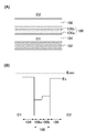
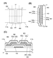
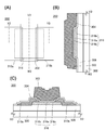
도 1의 (A)는 본 발명의 일 형태에 따른 반도체 장치에 포함되는 적층 구조의 일례를 도시한 모식도다. 본 발명의 일 형태에 따른 반도체 장치는 게이트 전극층(102)과, 게이트 전극층(102) 위의 게이트 절연층(104)과, 게이트 절연층(104) 위의 산화물 반도체층(106)과, 산화물 반도체층(106) 위의 절연층(108)으로 이루어지는 적층 구조를 포함한다.1 (A) is a schematic diagram showing an example of a laminated structure included in a semiconductor device according to an embodiment of the present invention. A semiconductor device according to an embodiment of the present invention includes a
산화물 반도체층(106)은 제 1 층(106a)과, 제 1 층(106a)과 절연층(108) 사이의 제 2 층(106b)으로 이루어지는 적층 구조를 갖는다.The
제 1 층(106a) 및 제 2 층(106b)은 거시적으로 보면 원자 배열에 주기성이 보이지 않을 정도로 매우 미세한 결정부를 포함하는 산화물 반도체층이다. 구체적으로는, 제 1 층(106a) 및 제 2 층(106b)은 각각 1nm 이상 10nm 이하, 또는 1nm 이상 3nm 이하의 크기를 갖는 결정부(이하, 본 명세서 등에서 나노 결정(nc: nano crystal)이라고 표기함)를 포함한다.The
제 1 층(106a) 및 제 2 층(106b)에 포함되는 결정부는 상기 결정부의 크기에 가깝거나 또는 결정부의 크기보다 작은 프로브 직경(예를 들어, 1nm 이상 30nm 이하)을 갖는 전자빔을 조사하여 얻어지는 전자빔 회절 패턴에서 휘도가 높은 원형(환형) 영역을 갖고 휘도가 높은 영역 내에 복수의 스폿(휘점)을 확인할 수 있다. 복수의 스폿이 원주로 배치됨으로써 휘도가 높은 환형 영역을 형성한다고 바꿔 말할 수 있다.The crystal portion included in the
또한, 포함되는 결정부의 크기에 가까운 범위 이하, 또는 결정부의 크기보다 작은 범위 이하로 전자빔 회절에 의한 평면 방향의 측정 범위 및 깊이 방향의 측정 범위를 축소함으로써 전자빔 회절 패턴에서 결정 상태를 나타내는 규칙성을 갖는 스폿이 관찰되는 경우가 있다. 평면 방향의 측정 범위를 축소하기 위해서는 전자빔의 프로브 직경을 축소(예를 들어, 1nm 이상 30nm 이하)하면 좋다. 또한, 깊이 방향의 측정 범위를 축소하기 위해서는 예를 들어, 이온 밀링 가공 등에 의하여 10nm 이하까지 박편화된 영역을 측정하면 좋다.It is also possible to reduce the measurement range in the plane direction and the depth direction by the electron beam diffraction to a range not more than a range close to the size of the crystal portion included or smaller than a range smaller than the size of the crystal portion to narrow the regularity indicating the crystal state in the electron beam diffraction pattern May be observed in some cases. In order to reduce the measurement range in the plane direction, the probe diameter of the electron beam may be reduced (for example, 1 nm or more and 30 nm or less). In order to reduce the measurement range in the depth direction, it is preferable to measure the thinned region to 10 nm or less by, for example, ion milling.
또한, 제 1 층(106a) 및 제 2 층(106b) 양쪽 모두의 단면 방향 및 평면 방향의 전자빔 회절 패턴에서 상술한 휘도가 높은 환형 영역 내에 배치된 복수의 스폿을 확인할 수 있다. 결정부가 단면 방향 또는 평면 방향의 지향성을 갖지 않고 막 중에 랜덤하게 포함됨으로써 단면 방향의 전자빔 회절 패턴에서 확인되는 스폿과 평면 방향의 전자빔 회절 패턴에서 확인되는 스폿은 같은 경향을 나타낸다.It is also possible to identify a plurality of spots arranged in the annular region having a high luminance in the electron beam diffraction pattern in both the cross-sectional direction and the planar direction of both the
또한, 산화물 반도체층 중에 포함되는 결정부가 10nm 이하이며 사용하는 프로브 직경보다 큰 결정부를 가지면 단면 방향과 평면 방향의 전자빔 회절 패턴에서 상이한 경향이 보일 수 있다. 예를 들어, 단면 방향에 프로브 직경보다 큰 원자 배열의 주기성을 갖고 평면 방향에 프로브 직경과 같거나 프로브 직경보다 작은 원자 배열의 주기성을 갖는 결정부를 측정하는 경우, 단면 방향의 전자빔 회절 패턴에서 확인되는 스폿은 평면 방향의 전자빔 회절 패턴에서 확인되는 스폿보다 희미하게 될 수 있다. 또한, 제 1 층(106a) 및 제 2 층(106b)은 각각 단면 방향 및 평면 방향의 전자빔 회절 패턴의 경향이 마찬가지인 영역과 상이한 경향이 보일 수 있는 영역을 갖는 경우가 있다. 예를 들어, 제 1 층(106a)과 제 2 층(106b)의 계면 근방에서는 단면 방향 및 평면 방향의 전자빔 회절 패턴이 상이한 경향을 나타내고, 제 1 층(106a)과 게이트 절연층(104)의 계면 근방에서는 단면 방향 및 평면 방향의 전자빔 회절 패턴이 마찬가지의 경향을 나타내는 경우가 있다.Further, when the crystal part included in the oxide semiconductor layer has a crystal part of 10 nm or less and larger than the diameter of the probe to be used, the electron beam diffraction pattern in the cross-sectional direction and the planar direction may be different. For example, in the case of measuring a crystal portion having a periodicity of an atomic arrangement larger than the probe diameter in the cross-sectional direction and having a periodicity of an atomic arrangement equal to or smaller than the probe diameter in the planar direction, it is confirmed in the electron beam diffraction pattern in the cross- The spot may become more blurred than the spot identified in the electron beam diffraction pattern in the planar direction. In some cases, the
또한, 상술한 바와 같이, 제 1 층(106a) 및 제 2 층(106b)에서 원자 배열에 주기성을 갖는 영역은 예를 들어, 1nm 이상 10nm 이하의 미소한 범위이며 또한, 상이한 결정부 사이에서는 결정 범위에 질서성이 보이지 않는다. 따라서 제 1 층(106a) 및 제 2 층(106b)은 각각 막 전체에서 배향성이 보이지 않는다. 그러므로 산화물 반도체층(106)의 분석 방법에 따라서는 제 1 층(106a) 및 제 2 층(106b)에 포함되는 결정부를 해석할 수 없어 비정질 산화물 반도체층과 구별할 수 없는 경우가 있다.In addition, as described above, the region having the periodicity in the atomic arrangement in the
예를 들어, 결정부를 포함하는 제 1 층(106a) 또는 제 2 층(106b)을 각각 단면 방향 및 평면 방향으로부터 투과형 전자 현미경(TEM: Transmission Electron Microscope)으로 관찰하여도 결정 구조를 명확히 확인하기 어렵다.For example, even if the
또한, 산화물 반도체층(106)에 대하여 제 1 층(106a) 및 제 2 층(106b)에 포함되는 결정부보다 큰 직경을 갖는 X선을 사용하는 X선 회절(XRD: X-Ray Diffraction) 장치를 사용하여 구조 해석을 수행하면 out-of-plane법에 의한 해석에서는 결정면을 나타내는 피크가 검출되지 않는다.An X-ray diffraction (XRD) device using an X-ray having a diameter larger than that of the crystal part included in the
더구나 제 1 층(106a) 또는 제 2 층(106b)에 대하여 결정부보다 프로브 직경이 큰(예를 들어, 100nm 이상) 전자빔을 사용하는 전자빔 회절(제한 시야 전자빔 회절이라고도 함)에서는 헤일로 패턴(halo pattern)과 같은 회절 패턴이 관측될 수 있다.Furthermore, in the electron beam diffraction (also referred to as limited viewing electron beam diffraction) using an electron beam having a larger probe diameter (for example, 100 nm or more) than the crystal portion with respect to the
또한, 전자빔의 프로브 직경을 크게 할수록 상술한 휘도가 높은 환형 영역이 희미하게 되어 환이 갖는 폭이 넓게 되는 것을 확인할 수 있다. 또한, 프로브 직경을 예를 들어, 50nm 이상으로 하면 휘도가 높은 환형 영역 내에 스폿을 관찰하기 어려워진다.Also, it can be seen that as the probe diameter of the electron beam is increased, the annular region having a higher luminance described above becomes faint and the width of the ring becomes wider. Further, when the probe diameter is, for example, 50 nm or more, it becomes difficult to observe the spot in the annular region having a high luminance.
본 실시형태에서 기재하는 나노 결정을 포함하는 산화물 반도체층(이하, 나노 결정 산화물 반도체층이라고도 표기함)은 비정질 산화물 반도체층에 비하여 막 밀도가 높고 치밀한 막이다. 산화물 반도체층은 결함이 적을수록 또는 수소 등의 불순물 농도가 낮을수록 막 밀도가 높게 된다. 산소 결함 및/또는 수소 등의 불순물은 산화물 반도체층에 결함 준위를 생성하는 요인이 되기 때문에 나노 결정을 포함하는 제 1 층(106a) 및 제 2 층(106b)은 비정질 산화물 반도체층에 비하여 결함 준위 밀도가 저감된 영역이라고 할 수 있다. 또한, 본 명세서 등에서 비정질 산화물 반도체층이란 예를 들어, 원자 배열이 무질서하고 결정 성분을 갖지 않는 산화물 반도체층을 가리킨다.The oxide semiconductor layer containing nanocrystals (hereinafter also referred to as a nanocrystalline oxide semiconductor layer) described in this embodiment is a dense film having a film density higher than that of the amorphous oxide semiconductor layer. The oxide semiconductor layer has a higher film density as the number of defects is smaller or the impurity concentration such as hydrogen is lower. Since the impurity such as oxygen defects and / or hydrogen is a cause of generating a defect level in the oxide semiconductor layer, the
또한, 제 1 층(106a) 및 제 2 층(106b)에는 적어도 인듐 및 아연을 구성 원소로서 갖는 금속 산화물을 사용하는 것이 바람직하다. 또한, 제 1 층(106a) 및 제 2 층(106b)의 구성 원소를 동일하게 하고 이들의 조성을 상이하게 하여도 좋다.It is preferable to use a metal oxide having at least indium and zinc as constituent elements in the
또한, 본 실시형태에서 제 1 층(106a) 및 제 2 층(106b)은 적어도 인듐 및 아연을 포함하는 나노 결정 산화물 반도체층이며 재료나 성막 조건에 따라서는 각 영역끼리의 계면이 불명확하게 되는 경우도 있다. 따라서 도 1에서는 제 1 층(106a)과 제 2 층(106b)의 계면을 모식적으로 점선으로 도시하였다. 이것은 나중에 제시되는 각 도면에서도 마찬가지다.In the present embodiment, the
제 1 층(106a)이 In-M-Zn 산화물(M은 Al, Ga, Ge, Y, Zr, Sn, La, Ce, 또는 Hf)로 표기되는 산화물 반도체층인 경우, 제 2 층(106b)으로서는 제 1 층(106a)과 마찬가지로 In-M-Zn 산화물(M은 Al, Ga, Ge, Y, Zr, Sn, La, Ce, 또는 Hf)로 표기되고 제 1 층(106a)보다 인듐에 대한 M의 원자수비가 높은 산화물 반도체층으로 하는 것이 바람직하다.In the case where the
더 구체적으로는, 제 2 층(106b)으로서 제 1 층(106a)보다 상술한 원소를 1.5배 이상, 바람직하게는 2배 이상, 더 바람직하게는 3배 이상 높은 원자수비로 포함하는 산화물 반도체층을 적용한다. 상술한 원소 M은 인듐보다 산소와 강하게 결합되기 때문에 인듐에 대한 M의 원자수비가 높은 산화물 반도체는 막 중에 산소 결손이 생기기 어렵다. 즉 제 2 층(106b)은 제 1 층(106a)보다 산소 결손이 생기기 어려운 산화물 반도체층이다. 또한, 인듐에 대한 M의 원자수비가 높을수록 산화물 반도체층의 에너지 갭(밴드 갭)이 커지기 때문에 인듐에 대한 M의 원자수비가 지나치게 높으면 제 2 층(106b)은 절연층으로서 기능한다. 따라서 제 2 층(106b)이 반도체층으로서 기능할 수 있도록 인듐에 대한 M의 원자수비를 조정하는 것이 바람직하다.More specifically, as the
제 1 층(106a) 및 제 2 층(106b)이 각각 적어도 인듐, 아연, 및 M(M은 Al, Ti, Ga, Ge, Y, Zr, Sn, La, Ce, 또는 Hf 등의 금속)을 포함하는 In-M-Zn 산화물이라면 제 1 층(106a)을 In:M:Zn=x1:y1:z1[원자수비], 제 2 층(106b)을 In:M:Zn=x2:y2:z2[원자수비]로 하면 y2/x2를 y1/x1보다 크게 하는 것이 바람직하다. y2/x2는 y1/x1보다 1.5배 이상, 바람직하게는 2배 이상, 더 바람직하게는 3배 이상으로 한다. 이 때, 제 1 층(106a)에서 y1이 x1 이상이라면 트랜지스터의 전기 특성을 안정시킬 수 있다. 다만 y1이 x1의 3배 이상이 되면 트랜지스터의 전계 효과 이동도가 저하되기 때문에 y1은 x1의 3배 미만인 것이 바람직하다.The
또한, 제 1 층(106a)이 In-M-Zn 산화물일 때, Zn과 O를 제외한 In과 M의 원자수 비율은 바람직하게는 In을 25atomic% 이상, M을 75atomic% 미만, 더 바람직하게는 In을 34atomic% 이상, M을 66atomic% 미만으로 한다. 또한, 제 2 층(106b)이 In-M-Zn 산화물일 때, Zn과 O를 제외한 In과 M의 원자수 비율은 바람직하게는 In을 50atomic% 미만, M을 50atomic% 이상, 더 바람직하게는 In을 25atomic% 미만, M을 75atomic% 이상으로 한다.When the
또한, 제 2 층(106b)은 전도대 하단의 에너지가 제 1 층(106a)의 그것보다 0.05eV, 0.07eV, 0.1eV, 0.15eV 중 어느 하나 이상이고 2eV, 1eV, 0.5eV, 0.4eV 중 어느 하나 이하만큼 진공 준위에 가까운 산화물 반도체로 형성되는 것이 바람직하다.The energy of the lower end of the conduction band of the
이와 같은 구조에서 게이트 전극층(102)에 전계를 인가하면 산화물 반도체층(106) 중 전도대 하단의 에너지가 가장 작은 층인 제 1 층(106a)이 캐리어의 주된 이동 경로(채널)가 된다. 여기서 채널 형성 영역(제 1 층(106a))과 절연층(108) 사이에 제 2 층(106b)을 포함함으로써 산화물 반도체층(106)과 절연층(108)의 계면에서 불순물 및 결함에 의하여 형성될 수 있는 트랩 준위와 채널 형성 영역 사이에 거리가 있다. 이 결과, 제 1 층(106a)을 흐르는 전자가 트랩 준위에 포획되기 어렵고, 트랜지스터의 온 전류를 증대시킬 수 있음과 동시에, 전계 효과 이동도를 높일 수 있다. 또한, 트랩 준위에 전자가 포획되면 상기 전자가 마이너스의 고정 전하가 되고 트랜지스터의 문턱 전압의 변동 요인이 된다. 그러나, 제 1 층(106a)과 트랩 준위 사이에 거리가 있기 때문에 트랩 준위에서 전자가 포획되는 것을 저감시킬 수 있어 문턱 전압의 변동을 저감시킬 수 있다.When an electric field is applied to the
또한, 제 1 층(106a) 및 제 2 층(106b)은 각 층을 단순히 적층시키는 것이 아니라 연속 접합(여기서는 특히 전도대 하단의 에너지가 각 층 사이에서 연속적으로 변화되는 구조를 가리킴)이 형성되도록 제작한다. 즉, 각 층의 계면에서 트랩 중심이나 재결합 중심과 같은 결함 준위를 형성하는 바와 같은 불순물이 존재하지 않는 적층 구조로 한다. 가령 적층된 제 1 층(106a)과 제 2 층(106b) 사이에 불순물이 혼재되면 에너지 밴드의 연속성이 없어져 계면에서 캐리어가 포획되거나 재결합하여 소멸된다.The
연속 접합을 형성하기 위해서는 로드록(load lock)실을 구비한 멀티 챔버 방식의 성막 장치(스퍼터링 장치)를 사용하여 각 막을 대기에 노출시키지 않고 연속적으로 적층할 필요가 있다. 스퍼터링 장치의 각 챔버는, 산화물 반도체층에서 불순물이 되는 물 등을 가능한 한 제거하기 위하여 크라이오 펌프와 같은 흡착식 진공 배기 펌프를 사용하여 고진공 배기(5×10⁻⁷Pa~1×10⁻⁴Pa 정도까지)하는 것이 바람직하다. 또는 터보 분자 펌프와 콜드 트랩을 조합하여 배기계로부터 챔버 내에 가스, 특히 탄소 또는 수소를 포함하는 가스가 역류하지 않도록 해 두는 것이 바람직하다.In order to form a continuous junction, it is necessary to sequentially laminate the films without exposing them to the atmosphere by using a multi-chamber type film forming apparatus (sputtering apparatus) provided with a load lock chamber. Each chamber of the sputtering apparatus is subjected to a high-vacuum discharge (5 x 10 < -7 > Pa to 1 x 10 < -4 > Pa ). Alternatively, it is preferable to combine the turbo molecular pump and the cold trap so that the gas, particularly the gas containing carbon or hydrogen, does not flow back into the chamber from the exhaust system.
도 1의 (B)는, 도 1의 (A)에 도시된 적층 구조를 D1-D2에서 잘랐을 때의 밴드 구조의 일부를 모식적으로 도시한 것이다. 여기서는 산화물 반도체층(106)과 접촉하는 절연층인 게이트 절연층(104) 및 절연층(108)으로서 산화 실리콘층을 제공한 경우에 대하여 설명한다. 또한, 도 1의 (B)에서 Evac는 진공 준위의 에너지를 가리키고 Ec는 전도대 하단의 에너지를 가리킨다.Fig. 1B schematically shows a part of the band structure when the laminated structure shown in Fig. 1A is cut in D1-D2. Here, the case of providing the silicon oxide layer as the
도 1의 (B)에 도시된 바와 같이, 제 1 층(106a) 및 제 2 층(106b)에서, 전도대 하단의 에너지는 장벽이 없고 완만하게 변화한다. 바꿔 말하면 연속적으로 변화한다고 할 수도 있다. 이것은 제 1 층(106a) 및 제 2 층(106b)이 공통적인 원소를 포함하고 제 1 층(106a)과 제 2 층(106b) 사이에서 산소가 상호적으로 이동함으로써 혼합층이 형성되기 때문이라고 할 수 있다.As shown in Fig. 1B, in the
도 1의 (B)를 보면 산화물 반도체층(106)에서 제 1 층(106a)이 웰(우물)이 되고 채널 영역이 제 1 층(106a)에 형성되는 것을 알 수 있다. 또한, 산화물 반도체층(106)은 전도대 하단의 에너지가 연속적으로 변화하기 때문에, 제 1 층(106a)과 제 2 층(106b)이 연속 접합한다고 할 수도 있다.Referring to FIG. 1B, it can be seen that in the
제 2 층(106b)과 절연층(108)의 계면 근방에는 절연층(108)의 구성 원소(예를 들어, 실리콘) 또는 탄소 등의 불순물이나 결함에 기인한 트랩 준위가 형성될 수 있지만 채널이 형성되는 제 1 층(106a)과 절연층(108) 사이에 제 2 층(106b)이 제공됨으로써 제 1 층(106a)과 트랩 준위를 멀어지게 할 수 있다. 다만, 제 1 층(106a)과 제 2 층(106b) 사이의 에너지 차이가 작은 경우, 제 1 층(106a)의 전자가 상기 에너지 차이를 넘어 트랩 준위에 도달되는 경우가 있다. 트랩 준위에 전자가 포획됨으로써 절연막 계면에 마이너스의 고정 전하가 생겨 트랜지스터의 문턱 전압은 플러스 방향으로 변동된다. 따라서, 제 1 층(106a)과 제 2 층(106b)의 전도대 하단의 에너지 차이를, 0.05eV 이상, 바람직하게는 0.15eV 이상으로 하면, 트랜지스터의 문턱 전압의 변동이 저감되어, 안정된 전기 특성이 되기 때문에 바람직하다.A trap level due to impurities or defects such as constituent elements (e.g., silicon) or carbon of the insulating
산화물 반도체층을 사용한 반도체 장치의 신뢰성을 향상시키기 위해서는 채널로서 기능하는 산화물 반도체층 및 그 계면의 결함 준위 밀도를 저감할 필요가 있다. 특히 산화물 반도체층을 사용한 트랜지스터의 문턱 전압이 마이너스 방향으로 변동하는 것은 채널로서 기능하는 산화물 반도체층 및 그 계면의 산소 결손에 기인하는 결함 준위가 원인이라고 생각될 수 있다.In order to improve the reliability of the semiconductor device using the oxide semiconductor layer, it is necessary to reduce the defect level density of the oxide semiconductor layer functioning as a channel and its interface. In particular, it is considered that the threshold voltage of the transistor using the oxide semiconductor layer fluctuates in the minus direction due to the oxide semiconductor layer functioning as a channel and the defect level due to the oxygen deficiency at the interface thereof.
그래서 본 실시형태에 기재된 바와 같이, 비정질 산화물 반도체층에 비하여 결함 준위 밀도가 저감된 제 1 층(106a) 및 제 2 층(106b)을 포함하는 산화물 반도체층을 트랜지스터에 사용함으로써 상기 트랜지스터의 가시광이나 자외광의 조사로 인한 전기 특성의 변동을 저감시킬 수 있다. 따라서 상기 트랜지스터의 신뢰성을 향상시킬 수 있다.Therefore, as described in this embodiment mode, by using the oxide semiconductor layer including the
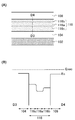
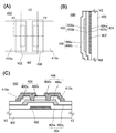
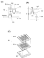
도 2의 (A)는 본 발명의 일 형태에 따른 반도체 장치에 포함되는 적층 구조의 다른 일례를 도시한 모식도다. 도 2의 (A)에 도시된 적층 구조는 도 1의 (A)에 도시된 적층 구조와 마찬가지로 게이트 전극층(102)과, 게이트 전극층(102) 위의 게이트 절연층(104)과, 게이트 절연층(104) 위의 산화물 반도체층(116)과, 산화물 반도체층(116) 위의 절연층(108)을 포함하고, 산화물 반도체층(116)은 채널이 형성되는 제 1 층(116a)과, 제 1 층(116a)과 절연층(108) 사이의 제 2 층(116b)과, 제 1 층(116a)과 게이트 절연층(104) 사이의 제 3 층(116c)을 포함한다.2 (A) is a schematic diagram showing another example of a laminated structure included in a semiconductor device according to an embodiment of the present invention. 2A, the
도 2의 (A)에 포함되는 산화물 반도체층(116)은 채널로서 기능하는 제 1 층(116a)과 게이트 절연층(104) 사이에 제 3 층(116c)을 포함하는 점이 도 1의 (A)에 도시된 산화물 반도체층(106)과 상이하고 그 외의 구성은 도 1의 (A)와 마찬가지로 할 수 있다. 예를 들어, 산화물 반도체층(116)의 제 1 층(116a)은 상술한 산화물 반도체층(106)의 제 1 층(106a)에 대한 설명을 참조할 수 있고 산화물 반도체층(116)의 제 2 층(116b)은 상술한 산화물 반도체층(106)의 제 2 층(106b)에 대한 설명을 참조할 수 있다.The
산화물 반도체층(116)에 포함되는 제 1 층(116a), 제 2 층(116b), 및 제 3 층(116c)은 각각 나노 결정을 포함하는 산화물 반도체층이다. 또한, 제 3 층(116c)은 제 1 층(116a) 및 제 2 층(116b)과 마찬가지로 적어도 인듐 및 아연을 구성 원소로서 갖는 금속 산화물을 사용하는 것이 바람직하다. 또한, 제 1 층(116a)~제 3 층(116c)의 구성 원소를 동일하게 하고 각 조성을 상이하게 하여도 좋다.The
제 1 층(116a)이 In-M-Zn 산화물(M은 Al, Ga, Ge, Y, Zr, Sn, La, Ce, 또는 Hf)로 표기되는 산화물 반도체층인 경우, 제 3 층(116c)으로서는 제 1 층(116a)과 마찬가지로 In-M-Zn 산화물(M은 Al, Ga, Ge, Y, Zr, Sn, La, Ce, 또는 Hf)로 표기되고 제 1 층(116a)보다 인듐에 대한 M의 원자수비가 높은 산화물 반도체층으로 하는 것이 바람직하다. 즉 제 3 층(116c)은 제 1 층(116a)보다 산소 결손이 생기기 어려운 산화물 반도체층이다. 더 구체적으로는, 제 3 층(116c)으로서 제 1 층(116a)보다 상술한 원소를 1.5배 이상, 바람직하게는 2배 이상, 더 바람직하게는 3배 이상 높은 원자수비로 포함하는 산화물 반도체층을 적용한다.When the
또한, 제 1 층(116a)~제 3 층(116c)이 각각 적어도 인듐, 아연, 및 M(M은 Al, Ti, Ga, Ge, Y, Zr, Sn, La, Ce, 또는 Hf 등의 금속)을 포함하는 In-M-Zn 산화물이라면 제 1 층(116a)을 In:M:Zn=x1:y1:z1[원자수비], 제 2 층(116b)을 In:M:Zn=x2:y2:z2[원자수비], 및 제 3 층(116c)을 In:M:Zn=x3:y3:z3[원자수비]으로 하면, y2/x2 및 y3/x3이 y1/x1보다 크게 되는 것이 바람직하다. y2/x2 및 y3/x3은 y1/x1보다 1.5배 이상, 바람직하게는 2배 이상, 더 바람직하게는 3배 이상으로 한다. 이 때, 제 1 층(116a)에서 y1이 x1 이상이라면 트랜지스터의 전기 특성을 안정시킬 수 있다. 다만 y1이 x1의 3배 이상이 되면 트랜지스터의 전계 효과 이동도가 저하되기 때문에 y1은 x1의 3배 미만인 것이 바람직하다.The
또한, 제 3 층(116c)이 In-M-Zn 산화물일 때, Zn과 O를 제외한 In과 M의 원자수 비율은 바람직하게는 In을 50atomic% 미만, M을 50atomic% 이상, 더 바람직하게는 In을 25atomic% 미만, M을 75atomic% 이상으로 한다. 또한, 제 1 층(116a)이 In-M-Zn 산화물일 때, Zn과 O를 제외한 In과 M의 원자수 비율은 바람직하게는 In을 25atomic% 이상, M을 75atomic% 미만, 더 바람직하게는 In을 34atomic% 이상, M을 66atomic% 미만으로 한다. 또한, 제 2 층(116b)이 In-M-Zn 산화물일 때, Zn과 O를 제외한 In과 M의 원자수 비율은 바람직하게는 In을 50atomic% 미만, M을 50atomic% 이상, 더 바람직하게는 In을 25atomic% 미만, M을 75atomic% 이상으로 한다. When the
또한, 제 3 층(116c)과 제 2 층(116b)은, 상이한 구성 원소를 포함하는 층으로 하여도 좋고, 동일한 구성 원소를 동일한 원자수비로, 또는 다른 원자수비로 포함하는 층으로 하여도 좋다.The
또한, 제 2 층(116b) 및 제 3 층(116c)은 전도대 하단의 에너지가 제 1 층(116a)의 그것보다 0.05eV, 0.07eV, 0.1eV, 0.15eV 중 어느 하나 이상이고 2eV, 1eV, 0.5eV, 0.4eV 중 어느 하나 이하만큼 진공 준위에 가까운 산화물 반도체로 형성되는 것이 바람직하다.The
도 2의 (B)는 도 2의 (A)에 도시된 적층 구조를 D3-D4에서 잘랐을 때의 밴드 구조의 모식도를 도시한 것이다.FIG. 2B is a schematic diagram of the band structure when the laminated structure shown in FIG. 2A is cut in D3-D4.
도 2의 (B)를 보면 산화물 반도체층(116)에서 제 1 층(116a)이 웰(우물)이 되고 채널 영역이 제 1 층(116a)에 형성되는 것을 알 수 있다. 또한, 산화물 반도체층(116)은 전도대 하단의 에너지가 연속적으로 변화하기 때문에, 제 1 층(116a), 제 2 층(116b), 및 제 3 층(116c)이 연속 접합한다고 할 수도 있다.Referring to FIG. 2B, it can be seen that the
채널로서 기능하는 제 1 층(116a)의 위 및 아래에 제공되는 제 2 층(116b) 또는 제 3 층(116c)은 배리어층으로서 기능하고 산화물 반도체층(116)에 접촉되는 절연층(게이트 절연층(104) 및 절연층(108))과 산화물 반도체층(116)의 계면에 형성되는 트랩 준위가, 트랜지스터의 캐리어의 주된 경로(캐리어 패스)가 되는 제 1 층(106a)에 미치는 영향을 억제할 수 있다.A
예를 들어, 산화물 반도체층에 포함되는 산소 결손은, 산화물 반도체의 에너지 갭 내의 깊은 에너지 위치에 존재하는 국재 준위(局在 準位)로서 현재화(顯在化)된다. 이와 같은 국재 준위에 캐리어가 포획됨으로써 트랜지스터의 신뢰성이 저하되기 때문에, 산화물 반도체층에 포함되는 산소 결손을 저감하여야 한다. 도 2에 도시된 적층 구조에서는 제 1 층(116a)에 비하여 산소 결손이 생기기 어려운 산화물 반도체층인 제 2 층(116b) 및 제 3 층(116c)을 제 1 층(116a)의 위 및 아래에 접촉하도록 제공함으로써 채널로서 기능하는 제 1 층(116a)에서의 산소 결손을 저감시킬 수 있다.For example, the oxygen deficiency contained in the oxide semiconductor layer is exposed as a local level existing at a deep energy position in the energy gap of the oxide semiconductor. Since the carrier is trapped at such a local level, the reliability of the transistor is lowered. Therefore, the oxygen deficiency contained in the oxide semiconductor layer must be reduced. 2, the
또한, 산화물 반도체층(116)이, 구성 원소가 상이한 절연층(예를 들어, 산화 실리콘막을 포함하는 하지 절연층)과 접촉하는 경우, 2층의 계면에 계면 준위가 형성되고, 상기 계면 준위는 채널을 형성하는 경우가 있다. 이와 같은 경우, 문턱 전압이 상이한 제 2 트랜지스터가 출현하여, 트랜지스터의 외견상 문턱 전압이 변동되는 경우가 있다. 하지만 도 2에 도시된 적층 구조를 포함하는 트랜지스터에서는 제 1 층(116a)~제 3 층(116c)은 각각 적어도 인듐 및 아연을 포함하여 구성되기 때문에 채널로서 기능하는 제 1 층(116a) 계면에 계면 준위를 형성하기 어렵게 된다. 따라서 트랜지스터의 문턱 전압 등의 전기 특성의 편차를 저감할 수 있다.Further, when the
또한, 게이트 절연층(104)과 산화물 반도체층(116)의 계면에 채널이 형성되는 경우, 상기 계면에서 계면 산란이 일어나, 트랜지스터의 전계 효과 이동도가 낮게 된다. 하지만 본 실시형태에 따른, 적층 구조를 포함하는 트랜지스터에서는 채널이 형성되는 제 1 층(116a)과 게이트 절연층(104) 사이에 산화물 반도체를 포함하여 이루어지는 제 3 층(116c)이 제공되고 제 3 층(116c)과 제 1 층(116a) 계면에서는 캐리어가 산란되기 어렵다. 따라서 상기 트랜지스터의 전계 효과 이동도를 높게 할 수 있다.Further, when a channel is formed at the interface between the
또한, 제 3 층(116c) 및 제 2 층(116b)은 각각, 게이트 절연층(104) 및 절연층(108)의 구성 원소가 채널이 형성되는 제 1 층(116a)에 혼입되어 불순물에 의한 준위가 형성되는 것을 억제하기 위한 배리어층으로서도 기능한다.The
또한, 도 2의 (B)에서는 제 3 층(116c)의 전도대 하단의 에너지가 제 2 층(116b)의 전도대 하단의 에너지보다 진공 준위에 가까운 경우를 예로 들어 설명하였지만, 본 발명의 일 형태는 이것에 한정되지 않는다. 제 2 층(116b) 및 제 3 층(116c)은 각각 적어도 제 1 층(116a)의 전도대 하단의 에너지보다 진공 준위에 가까운 전도대 하단의 에너지를 가지면 좋고, 제 3 층(116c)은 제 2 층(116b)의 전도대 하단의 에너지보다 진공 준위로부터 멀어지는 전도대 하단의 에너지를 가져도 좋고, 양쪽이 같은 에너지를 가져도 좋다.2B, the case where the energy of the lower end of the conduction band of the
또한, 상술한 설명에서는 적어도 제 1 층 및 제 2 층을 포함하는 산화물 반도체층이 게이트 절연층을 개재하여 게이트 전극층 위에 제공된 보텀 게이트 구조에 대하여 기재하였지만 본 발명의 일 형태는 이에 한정되지 않는다.In the above description, the oxide semiconductor layer including at least the first layer and the second layer is described on the bottom gate structure provided on the gate electrode layer via the gate insulating layer, but one form of the present invention is not limited thereto.
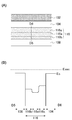
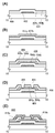
도 3의 (A)는 본 발명의 일 형태에 따른 반도체 장치에 포함되는 적층 구조의 다른 일례를 도시한 모식도다. 도 3의 (A)에 도시된 적층 구조는 절연층(108)과, 절연층(108) 위의 산화물 반도체층(116)과, 산화물 반도체층(116) 위의 게이트 절연층(104)과, 게이트 절연층(104) 위의 게이트 전극층(102)을 포함하고, 산화물 반도체층(116)은 채널이 형성되는 제 1 층(116a)과, 제 1 층(116a)과 절연층(108) 사이의 제 2 층(116b)과, 제 1 층(116a)과 게이트 절연층(104) 사이의 제 3 층(116c)을 포함한다.3 (A) is a schematic diagram showing another example of the laminated structure included in the semiconductor device according to one embodiment of the present invention. 3 (A) includes an insulating
또한, 도 3의 (B)는 도 3의 (A)에 도시된 적층 구조를 D5-D6에서 잘랐을 때의 밴드 구조의 일부를 모식적으로 도시한 것이다.FIG. 3B schematically shows a part of the band structure when the laminated structure shown in FIG. 3A is cut in D5-D6.
도 3에는, 도 2에 도시된 적층 구조의 적층 순서를 반대로 하여 톱 게이트 구조로 한 적층 구조를 예를 들어 도시하였다. 각 층이 갖는 구성은 상술한 설명과 마찬가지로 할 수 있다. 도 3에 도시된 톱 게이트 구조의 자세한 사항은 도 2에 대한 설명을 참조할 수 있고 같은 효과를 나타낼 수 있다.In FIG. 3, a stacked structure having a top gate structure is illustrated by reversing the stacking order of the stacked structure shown in FIG. 2, for example. The constitution of each layer can be the same as that described above. The details of the top gate structure shown in FIG. 3 can be referred to the description of FIG. 2 and can show the same effect.
또한, 도 3에서는 제 1 층(116a)의 위 및 아래에 제 2 층(116b) 및 제 3 층(116c)이 각각 접촉하도록 제공된 톱 게이트형 구조를 도시하였지만 본 발명의 일 형태는 이것에 한정되지 않는다. 예를 들어, 제 1 층(116a) 위에 접촉하도록 산화물 반도체층을 중첩되어 2층의 적층 구조로 이루어지는 산화물 반도체층을 제공하고, 이 2층의 적층 구조로 이루어지는 산화물 반도체층 위에 게이트 전극층을 갖는 톱 게이트형 구조를 적용하여도 좋다.Although FIG. 3 shows the top gate type structure provided so that the
상술한 바와 같이, 본 실시형태에 따른, 적층 구조를 포함하는 트랜지스터는 산화물 반도체층에서 채널이 형성되는 제 1 층과 절연층 사이에 제 2 층이 제공됨으로써 산화물 반도체층의 계면과 채널을 멀어지게 할 수 있기 때문에 계면 준위가 채널에 미치는 영향을 억제할 수 있다.As described above, in the transistor including the stacked structure according to the present embodiment, the second layer is provided between the first layer where the channel is formed in the oxide semiconductor layer and the insulating layer, so that the interface and the channel of the oxide semiconductor layer are separated from each other The influence of the interface level on the channel can be suppressed.
또한, 제 1 층(116a)~제 3 층(116c)은 비정질 산화물 반도체에 비하여 결함 준위 밀도가 저감된 나노 결정 산화물 반도체로 구성된다. 결함 준위 밀도가 저감된 제 1 층(116a)~제 3 층(116c)을 포함하는 산화물 반도체층을 트랜지스터에 사용함으로써 상기 트랜지스터의 전기 특성의 변동을 저감하고 신뢰성을 향상시킬 수 있다.The
(참고예)(Reference example)
본 참고예에서는 본 실시형태에 따른 산화물 반도체층에 포함되는 나노 결정에 대하여 나노 전자빔 회절 패턴을 사용하여 설명한다.In this reference example, nanocrystals contained in the oxide semiconductor layer according to the present embodiment will be described using a nano electron beam diffraction pattern.
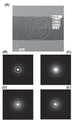
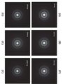
<산화물 반도체층의 단면 방향의 나노 전자빔 회절 패턴>≪ Nano electron beam diffraction pattern in the cross-sectional direction of the oxide semiconductor layer &
본 참고예에서 사용하는 시료 1의 제작 방법을 이하에서 기재한다. 제 1 층에 상당하는 산화물 반도체층의 일례로서, 석영 유리 기판 위에 In-Ga-Zn계 산화물막을 막 두께 50nm로 성막한 것을 시료 1로서 사용한다. 이 성막 조건은 In:Ga:Zn=1:1:1[원자수비]인 산화물 타깃을 사용하여, 산소 분위기 하(유량 45sccm), 압력 0.4Pa, 직류(DC) 전원 0.5kW, 기판 온도를 실온으로 하였다. 또한, 산화물 반도체층을 성막한 후 질소 분위기 하에서 450℃로 1시간 동안 제 1 가열 처리를 수행하고, 질소 및 산소 분위기 하에서 450℃로 1시간 동안 제 2 가열 처리를 수행하였다.The production method of the sample 1 used in this Reference Example is described below. As an example of the oxide semiconductor layer corresponding to the first layer, an In-Ga-Zn oxide film having a film thickness of 50 nm is formed on a quartz glass substrate as a sample 1. The deposition conditions were as follows: an oxide target having an In: Ga: Zn ratio of 1: 1: 1 (atomic ratio) was used and the substrate temperature was set at room temperature (flow rate: 45 sccm) Respectively. After the oxide semiconductor layer was formed, the first heat treatment was performed at 450 占 폚 for one hour in a nitrogen atmosphere, and the second heat treatment was performed at 450 占 폚 for one hour in an atmosphere of nitrogen and oxygen.
제 2 가열 처리를 수행한 후의 산화물 반도체층을 Ar이온을 사용한 이온 밀링법에 의하여 50nm 정도(40nm±10nm)가 되도록 박편화하였다. 먼저, 박편화를 보강하기 위하여 산화물 반도체층이 성막된 석영 유리 기판을 더미 기판과 접합한 후, 절단 및 연마에 의하여 두께 50μm 정도가 되도록 박편화하였다. 그 후, 도 5에 도시된 바와 같이, 산화물 반도체층(204)이 제공된 석영 유리 기판(200) 및 더미 기판(202)에 대하여 저각도(3° 정도)로부터 아르곤 이온을 조사하여 이온 밀링을 수행하고 50nm 정도(40nm±10nm)까지 박편화된 영역(210a)을 형성하고 그 단면을 관찰하였다.The oxide semiconductor layer after the second heat treatment was thinned to about 50 nm (40 nm ± 10 nm) by an ion milling method using Ar ions. First, a quartz glass substrate having an oxide semiconductor layer formed thereon was bonded to a dummy substrate to reinforce flaking, and then cut to a thickness of about 50 mu m by cutting and polishing. 5, ion milling is performed by irradiating argon ions from the low angle (about 3 deg.) To the
제 1 가열 처리 및 제 2 가열 처리를 수행한 후의 산화물 반도체층을 50nm 정도(40nm±10nm)가 되도록 박편화한 시료 1의 단면 TEM상을 도 4의 (A)에 나타내었다. 또한, 도 4의 (A)에 나타낸 단면을 나노 전자빔 회절에 의하여 측정한 전자빔 회절 패턴을 도 4의 (B)~(E)에 나타내었다. 도 4의 (B)는 프로브 직경을 1nm로 수속시킨 전자빔을 조사한 전자빔 회절 패턴이다. 도 4의 (C)는 프로브 직경을 10nm로 수속시킨 전자빔을 조사한 전자빔 회절 패턴이다. 도 4의 (D)는 프로브 직경을 20nm로 수속시킨 전자빔을 조사한 전자빔 회절 패턴이다. 그리고 도 4의 (E)는 프로브 직경을 30nm로 수속시킨 전자빔을 조사한 전자빔 회절 패턴이다.A cross-sectional TEM image of the sample 1 in which the oxide semiconductor layer after the first heat treatment and the second heat treatment were made thin to be about 50 nm (40 nm ± 10 nm) is shown in FIG. 4 (B) to 4 (E) show electron beam diffraction patterns measured by nano-electron beam diffraction of the cross section shown in Fig. 4 (A). 4B is an electron beam diffraction pattern irradiated with an electron beam converged at a probe diameter of 1 nm. 4C is an electron beam diffraction pattern irradiated with an electron beam converged at a probe diameter of 10 nm. 4 (D) is an electron beam diffraction pattern irradiated with an electron beam converged at a probe diameter of 20 nm. 4 (E) is an electron beam diffraction pattern irradiated with an electron beam converged at a probe diameter of 30 nm.
도 4의 (B)에 나타낸 바와 같이, 시료 1의 단면 방향의 전자빔 회절 패턴에서 휘도가 높은 환형 영역을 갖고 휘도가 높은 영역 내에 복수의 스폿(휘점)이 관찰된다. 또한, 도 4의 (C)~(E)를 보면 전자빔의 프로브 직경을 크게 하여 측정 범위를 넓히면 상기 복수의 스폿은 서서히 희미해지고 휘도가 높은 환형 영역의 폭도 넓어지는 것을 확인할 수 있다.As shown in Fig. 4 (B), a plurality of spots (bright spots) are observed in an area having a high luminance and a high luminance in the electron beam diffraction pattern in the cross-sectional direction of the sample 1. [ 4 (C) to 4 (E), it can be seen that as the probe diameter of the electron beam is increased and the measurement range is widened, the plurality of spots gradually become faint and the width of the annular region having a higher luminance is widened.
본 참고예의 시료 1에 포함되는 결정부의 크기가 10nm 이하, 또는 5nm 이하인 경우, 산화물 반도체층을 50nm 정도가 되도록 박편화한 시료 1에서는 깊이 방향의 측정 범위가 상기 결정부의 크기보다 크게 되기 때문에 측정 범위 내에 복수의 결정부가 포함될 수 있다. 그래서, 시료 1과 같은 제작 방법으로 제작한 산화물 반도체층이 10nm 이하, 바람직하게는 5nm 이하, 더 바람직하게는 3nm 이하까지 박편화된 영역을 시료 2로 하고 그 단면을 나노 전자빔 회절에 의하여 관찰하였다.When the size of the crystal part included in the sample 1 of this reference example is 10 nm or less, or 5 nm or less, the measurement range in the depth direction of the sample 1 in which the oxide semiconductor layer is thinned to be about 50 nm is larger than the size of the crystal part, A plurality of determination units may be included in the determination unit. Thus, the thinned region of the oxide semiconductor layer prepared by the same manufacturing method as that of the sample 1 to 10 nm or less, preferably 5 nm or less, more preferably 3 nm or less was used as the sample 2, and its cross section was observed by nano-electron beam diffraction .
Ar이온을 사용하여 이온 밀링법을 수행하고 도 5에 도시된 바와 같이, 10nm 이하(예를 들어, 5nm~10nm)까지 박편화된 영역(210b)을 형성하고, 이 단면을 관찰하였다.Ion milling was performed using Ar ions to form a
10nm 이하까지 박편화된 시료 2의 임의의 4점을, 프로브 직경을 1nm로 수속시킨 전자빔을 사용하여 측정한 나노 전자빔 회절 패턴을 도 6에 나타내었다.6 shows a nano electron beam diffraction pattern measured by using an electron beam obtained by converging any four points of the sample 2 thinned to 10 nm or less to 1 nm in probe diameter.
도 6의 (A) 및 (B)에서는 특정한 면으로 배향한 결정 상태를 나타내는 규칙성을 갖는 스폿을 관찰할 수 있다. 여기서부터 본 실시형태에 따른 산화물 반도체층은 결정부를 확실히 갖는 것을 알 수 있다. 한편으로, 도 6의 (C) 및 (D)에서는 휘도가 높은 환형 영역 내에 배치된 복수의 스폿을 관찰할 수 있다.6 (A) and 6 (B), a spot having a regularity indicating a crystal state oriented to a specific plane can be observed. From this, it can be seen that the oxide semiconductor layer according to the present embodiment reliably has a crystal portion. On the other hand, in FIGS. 6C and 6D, it is possible to observe a plurality of spots arranged in the annular region having a high luminance.
상술한 바와 같이, 나노 결정 산화물 반도체층에 포함되는 결정부의 크기는 예를 들어, 10nm 이하, 또는 5nm 이하로 매우 미세하다. 따라서 예를 들어, 시료를 10nm 이하가 되도록 박편화하고 전자빔을 1nm로 수속시켜 평면 방향의 측정 범위 및 깊이 방향의 측정 범위를 축소(예를 들어, 한 결정부 크기보다 작은 영역까지 축소)한 경우, 측정하는 영역에 따라서는 특정 면으로 배향한 결정 상태를 나타내는 규칙성을 갖는 스폿을 관찰할 수 있다. 또한, 측정하는 영역에 복수의 결정부가 포함되면 결정부를 투과한 전자빔이 결정의 크기보다 더 넓어짐으로써 깊이 방향의 결정의 스폿이 관측될 수 있다. 이 경우, 나노 전자빔 회절 패턴에서 복수의 스폿이 관측되는 것이 생각될 수 있다.As described above, the size of the crystal portion included in the nanocrystal oxide semiconductor layer is extremely small, for example, 10 nm or less, or 5 nm or less. Therefore, for example, when the sample is thinned to 10 nm or less and the electron beam is converged to 1 nm to reduce the measuring range in the plane direction and the measuring range in the depth direction (for example, , And a spot having a regularity indicating a crystal state oriented to a specific plane depending on the region to be measured can be observed. Further, when a plurality of crystal portions are included in the region to be measured, the electron beam transmitted through the crystal portion becomes wider than the crystal size, so that the spot of the crystal in the depth direction can be observed. In this case, it is conceivable that a plurality of spots are observed in the nano electron beam diffraction pattern.
다음에 시료 1 및 시료 2와 조성이 상이한 산화물 반도체층을 시료 3으로서 제작하고 나노 전자빔을 조사하여 전자빔 회절 패턴을 확인하였다. 시료 3은 본 실시형태에 따른 산화물 반도체층에서 제 2 층 또는 제 3 층에 상당하는 산화물 반도체층의 일례다.Next, an oxide semiconductor layer having a different composition from Sample 1 and Sample 2 was prepared as Sample 3 and an electron beam diffraction pattern was confirmed by irradiation with a nano electron beam. Sample 3 is an example of the oxide semiconductor layer corresponding to the second layer or the third layer in the oxide semiconductor layer according to the present embodiment.
시료 3의 제작 방법을 이하에 기재한다. 석영 유리 기판 위에 In-Ga-Zn계 산화물막을 막 두께 100nm로 형성한 것을 시료 3으로서 사용한다. 이 성막 조건은 In:Ga:Zn=1:3:2[원자수비]인 산화물 타깃을 사용하여, 산소 및 아르곤 분위기 하(산소 유량 15sccm, Ar 유량 30sccm), 압력 0.4Pa, 직류(DC) 전원 0.5kW, 기판 온도를 실온으로 하였다.A method for producing the sample 3 is described below. An In-Ga-Zn oxide film having a thickness of 100 nm formed on a quartz glass substrate is used as a sample 3. The deposition conditions were as follows: an oxide target having an In: Ga: Zn ratio of 1: 3: 2 (atomic ratio) was used and an oxygen and argon atmosphere (oxygen flow rate 15 sccm,
형성된 산화물 반도체층을 50nm 정도(40nm±10nm)가 되도록 박편화한 시료 3의 단면 TEM상을 도 7에 나타내었다. 또한, 도 7에 나타낸 단면을 나노 전자빔 회절에 의하여 측정한 전자빔 회절 패턴을 도 8에 나타내었다. 도 8의 (A)는 프로브 직경을 1nm로 수속시킨 전자빔을 조사한 전자빔 회절 패턴이다. 도 8의 (B)는 프로브 직경을 10nm로 수속시킨 전자빔을 조사한 전자빔 회절 패턴이다. 도 8의 (C)는 프로브 직경을 20nm로 수속시킨 전자빔을 조사한 전자빔 회절 패턴이다. 도 8의 (D)는 프로브 직경을 30nm로 수속시킨 전자빔을 조사한 전자빔 회절 패턴이다. 도 8의 (E)는 프로브 직경을 50nm로 수속시킨 전자빔을 조사한 전자빔 회절 패턴이다. 그리고 도 8의 (F)는 프로브 직경을 100nm로 수속시킨 전자빔을 조사한 전자빔 회절 패턴이다.FIG. 7 shows a cross-sectional TEM image of Sample 3 in which the formed oxide semiconductor layer was thinned to have a thickness of about 50 nm (40 nm 占 10 nm). The electron beam diffraction pattern measured by the nano-electron beam diffraction of the cross section shown in Fig. 7 is shown in Fig. 8A is an electron beam diffraction pattern irradiated with an electron beam converged at a probe diameter of 1 nm. 8B is an electron beam diffraction pattern irradiated with an electron beam converged at a probe diameter of 10 nm. FIG. 8C is an electron beam diffraction pattern irradiated with an electron beam converged at a probe diameter of 20 nm. 8 (D) is an electron beam diffraction pattern irradiated with an electron beam converged at a probe diameter of 30 nm. 8 (E) is an electron beam diffraction pattern irradiated with an electron beam converged at a probe diameter of 50 nm. 8 (F) is an electron beam diffraction pattern irradiated with an electron beam converged at a probe diameter of 100 nm.
도 8에 나타낸 바와 같이, 시료 1과 조성이 상이한 시료 3의 단면 방향의 전자빔 회절 패턴에서도 휘도가 높은 환형 영역을 갖고 휘도가 높은 영역 내에 복수의 스폿(휘점)이 관찰된다. 또한, 도 8을 보면 전자빔의 프로브 직경을 크게 하여 측정 범위를 넓히면 상기 복수의 스폿은 서서히 희미해지고 휘도가 높은 환형 영역의 폭도 넓어지는 것이 확인된다.As shown in Fig. 8, a plurality of spots (bright spots) are observed in an area having a high luminance and a high luminance even in the electron beam diffraction pattern in the cross-sectional direction of the sample 3 having a different composition from the sample 1. 8, when the probe diameter of the electron beam is increased and the measurement range is widened, it is confirmed that the plurality of spots gradually fade and the width of the annular region having a higher luminance is widened.
<석영 유리 기판에서의 나노 전자빔 회절 패턴>≪ Nano electron beam diffraction pattern on quartz glass substrate >
도 9에 석영 유리 기판에서의 나노 전자빔 회절 패턴을 나타내었다. 도 9의 측정 조건은 도 4의 (B) 및 도 8의 (A)와 마찬가지로 하고 전자빔의 프로브 직경을 1nm로 수속시켰다.FIG. 9 shows a nano electron beam diffraction pattern on a quartz glass substrate. The measurement conditions in Fig. 9 were the same as those in Figs. 4 (B) and 8 (A), and the probe diameter of the electron beam was converged to 1 nm.
도 9에 나타낸 바와 같이, 비정질 구조를 갖는 석영 유리 기판에서는 특정한 스폿으로 회절되지 않고, 메인 스폿으로부터 휘도가 연속적으로 변화하는 헤일로 패턴이 관측된다. 이와 같이, 비정질 구조를 갖는 막에서는 매우 미소한 영역의 전자빔 회절을 수행하더라도 본 실시형태에 따른 산화물 반도체층에서 관찰되는 바와 같은 원주로 배치된 복수의 스폿이 관찰되지 않는다. 따라서 본 참고예에 기재된 시료 1~시료 3에서 관찰되는 원주로 배치된 복수의 스폿은 본 참고예에 기재된 산화물 반도체층에 특유한 것이라고 확인된다.As shown in Fig. 9, in a quartz glass substrate having an amorphous structure, a halo pattern in which the luminance continuously changes from the main spot is not observed in a specific spot is observed. As described above, even when the electron beam diffraction in a very minute region is performed in the film having an amorphous structure, a plurality of spots arranged in a circumferential direction as observed in the oxide semiconductor layer according to the present embodiment is not observed. Therefore, it is confirmed that the plurality of spots arranged in the circumference as observed in Samples 1 to 3 described in this Reference Example are peculiar to the oxide semiconductor layer described in this Reference Example.
<산화물 반도체층의 단면 방향의 나노 전자빔 회절 패턴 및 평면 방향의 나노 전자빔 회절 패턴>≪ Nano electron beam diffraction pattern in the cross-sectional direction of the oxide semiconductor layer and nano electron beam diffraction pattern in the plane direction >
이어서 형성된 산화물 반도체층에 대하여 단면 방향 및 평면 방향으로부터 각각 전자빔을 조사한 전자빔 회절 패턴을 비교한다. 비교하기 위하여 사용한 시료 4의 제작 방법을 이하에 기재한다.Next, electron beam diffraction patterns obtained by irradiating electron beams from the cross-sectional direction and the planar direction with respect to the oxide semiconductor layer formed are compared. A method for producing the sample 4 used for comparison is described below.
석영 유리 기판 위에 In-Ga-Zn계 산화물막을 막 두께 50nm로 성막한 것을 시료 4로서 사용한다. 이 성막 조건은 In:Ga:Zn=1:1:1[원자수비]인 산화물 타깃을 사용하여, 산소 분위기 하(유량 45sccm), 압력 0.4Pa, 직류(DC) 전원 0.5kW, 기판 온도를 실온으로 하였다. An In-Ga-Zn-based oxide film having a film thickness of 50 nm is formed on a quartz glass substrate as a sample 4. The deposition conditions were as follows: an oxide target having an In: Ga: Zn ratio of 1: 1: 1 (atomic ratio) was used and the substrate temperature was set at room temperature (flow rate: 45 sccm) Respectively.
형성된 산화물 반도체층에 대하여 평면 방향으로부터 전자빔을 조사한 나노 전자빔 회절 패턴을 도 10의 (A)에 나타내었다. 또한, 산화물 반도체층을 50nm 정도가 되도록 박편화한 후, 단면 방향으로 전자빔을 조사한 나노 전자빔 회절 패턴을 도 10의 (B)에 나타내었다. 도 10의 (A) 및 (B)는 프로브 직경을 1nm로 수속시킨 전자빔을 조사한 전자빔 회절 패턴이다.Fig. 10 (A) shows a nano-electron beam diffraction pattern obtained by irradiating an electron beam from the planar direction to the oxide semiconductor layer formed. FIG. 10B shows a nano-electron beam diffraction pattern obtained by thinning the oxide semiconductor layer to a thickness of about 50 nm and irradiating an electron beam in the cross-sectional direction. 10 (A) and 10 (B) are electron beam diffraction patterns obtained by irradiating an electron beam converged at a probe diameter of 1 nm.
도 10의 (A) 및 (B)에 나타낸 바와 같이, 평면 방향의 전자빔 회절 패턴에서도 단면 방향의 전자빔 회절 패턴과 마찬가지로 휘도가 높은 환형 영역을 갖고 휘도가 높은 영역 내에 복수의 스폿(휘점)을 확인할 수 있다. 따라서 본 참고예에 기재된 시료 4에서는 막 중의 단면 방향 또는 평면 방향으로 치우치지 않고 대략 균일하게 결정부를 포함하는 곳이 확인되었다.As shown in Figs. 10A and 10B, in the electron beam diffraction pattern in the planar direction, a plurality of spots (bright spots) are observed in an area having a high luminance and a high luminance similarly to the electron beam diffraction pattern in the sectional direction . Therefore, in the sample 4 described in this Reference Example, it was confirmed that the crystal portion was not substantially deviated in the cross-sectional direction or the planar direction of the film but substantially uniformly included the crystal portion.
<X선 회절에 의한 분석>≪ Analysis by X-ray diffraction >
이어서 석영 유리 기판 위에 산화물 반도체층이 제공된 시료 5를 X선 회절(XRD: X-Ray Diffraction)을 사용하여 분석하였다. 도 11에 out-of-plane법을 사용하여 XRD 스펙트럼을 측정한 결과를 나타내었다. 또한, 시료 5의 제작 방법은 상술한 시료 4와 마찬가지다.Then, the sample 5 provided with the oxide semiconductor layer on the quartz glass substrate was analyzed using X-ray diffraction (XRD). FIG. 11 shows the result of XRD spectrum measurement using the out-of-plane method. The method of producing sample 5 is the same as that of sample 4 described above.
도 11에서 세로 축은 X선 회절 강도(임의 단위)이고, 가로 축은 회절각 2θ(deg.)다. 또한, XRD 스펙트럼의 측정에는 X선 회절 장치 D-8 ADVANCE(Bruker AXS사제)를 사용하였다.11, the vertical axis is the X-ray diffraction intensity (arbitrary unit), and the horizontal axis is the diffraction angle 2? (Deg.). An X-ray diffractometer D-8 ADVANCE (manufactured by Bruker AXS) was used for the measurement of the XRD spectrum.
도 11에 나타낸 바와 같이, 2θ=20°∼23° 근방에 석영에 기인하는 피크가 관찰되지만, 산화물 반도체층에 포함되는 결정부에 기인하는 피크는 확인되지 않는다. 따라서 도 11의 결과를 봐서도 본 참고예에 따른 산화물 반도체층에 포함되는 결정부는 매우 미세한 결정부인 것이 시사된다.As shown in Fig. 11, peaks due to quartz are observed in the vicinity of 2? = 20 to 23 占 but peaks attributable to crystal portions included in the oxide semiconductor layer are not confirmed. Therefore, it is suggested that the crystal part included in the oxide semiconductor layer according to the present reference example is a very fine crystal part, considering the results of FIG.
상술한 바와 같이, 본 실시형태에 따른 산화물 반도체층에 포함되는 결정부의 크기는 예를 들어, 10nm 이하, 또는 5nm 이하인 것이 추측된다. 본 실시형태에 따른 산화물 반도체층은 예를 들어, 1nm 이상 10nm 이하의 결정부(나노 결정)를 포함하는 산화물 반도체층이다.As described above, it is presumed that the size of the crystal portion included in the oxide semiconductor layer according to the present embodiment is, for example, 10 nm or less, or 5 nm or less. The oxide semiconductor layer according to the present embodiment is, for example, an oxide semiconductor layer containing crystal portions (nanocrystals) of 1 nm or more and 10 nm or less.
상술한 본 실시형태에 기재된 구성 및 방법 등은 다른 실시형태에 기재된 구성 및 방법 등과 적절히 조합하여 사용할 수 있다.The configuration and method described in the present embodiment can be used in combination with the configuration, the method, and the like described in the other embodiments.
(실시형태 2)(Embodiment 2)
본 실시형태에서는 실시형태 1에 기재된 적층 구조를 갖는 반도체 장치에 대하여 도 12~도 17을 참조하여 설명한다.In this embodiment mode, a semiconductor device having the laminated structure described in Embodiment Mode 1 will be described with reference to Figs. 12 to 17. Fig.
<트랜지스터의 구성예 1>≪ Configuration Example 1 of Transistor &
도 12에 반도체 장치의 구성예를 도시하였다. 도 12에서는 반도체 장치의 일례로서 보텀 게이트 구조의 트랜지스터를 도시하였다. 도 12의 (A)는 트랜지스터(450)의 평면도이고, 도 12의 (B)는 도 12의 (A)를 V1-W1을 따라 자른 단면도이고, 도 12의 (C)는 도 12의 (A)를 X1-Y1을 따라 자른 단면도다. 또한, 도면이 복잡해지는 것을 피하기 위하여 도 12의 (A)에서는 구성 요소의 일부(예를 들어, 절연층(408) 등)를 생략하여 도시하였다. 이것은 이후의 평면도에 관해서도 마찬가지다.12 shows a configuration example of the semiconductor device. In Fig. 12, a transistor having a bottom gate structure is shown as an example of a semiconductor device. 12A is a plan view of the
도 12에 도시된 트랜지스터(450)는 기판(400) 위에 제공된 게이트 전극층(402)과, 게이트 전극층(402) 위의 게이트 절연층(404)과, 게이트 절연층(404) 위에 제공되고 게이트 전극층(402)과 서로 중첩되는 산화물 반도체층(406)과, 산화물 반도체층(406)과 전기적으로 접속되는 소스 전극층(410a) 및 드레인 전극층(410b)과, 산화물 반도체층(406)을 개재하여 게이트 절연층(404)과 서로 중첩되는 절연층(408)을 포함한다.The
트랜지스터(450)에 포함되는 산화물 반도체층(406)은 채널이 형성되는 제 1 층(406a)과, 제 1 층(406a)과 절연층(408) 사이의 제 2 층(406b)의 적층 구조를 갖는다. 제 1 층(406a) 및 제 2 층(406b)은 각각 나노 결정을 포함하는 산화물 반도체층이고 도 1에 도시된 제 1 층(106a) 및 제 2 층(106b)에 각각 상당한다.The
상술한 바와 같이, 제 1 층(406a) 및 제 2 층(406b)은 각각 인듐 및 아연을 구성 원소로서 포함하고 제 2 층(406b)의 전도대 하단의 에너지는 제 1 층(406a)의 전도대 하단의 에너지보다 0.05eV 이상 2eV 이하만큼 진공 준위에 가깝다.As described above, the
제 1 층(406a) 및 제 2 층(406b)이 나노 결정을 포함함으로써 산화물 반도체층(406)은 비정질 산화물 반도체에 비하여 결함 준위 밀도가 저감된 산화물 반도체층으로 할 수 있다. 또한, 산화물 반도체층(406)에서 채널이 형성되는 제 1 층(406a)과 절연층(408) 사이에 제 2 층(406b)을 포함함으로써 산화물 반도체층(406)과 절연층(408) 사이에 형성될 수 있는 트랩 준위가 채널에 미치는 영향을 저감 또는 억제할 수 있다. 따라서 트랜지스터(450)의 전기 특성을 안정화시킬 수 있다.Since the
또한, 산화물 반도체층(406)에서 채널이 형성되는 제 1 층(406a)은 수소가 가능한 한 저감되는 것이 바람직하다. 구체적으로는 2차 이온 질량 분석법(SIMS: Secondary Ion Mass Spectrometry)에 의하여 얻어지는 제 1 층(406a)에서의 수소 농도는 2×10²⁰atoms/cm3 이하, 바람직하게는 5×10¹⁹atoms/cm3 이하, 1×10¹⁹atoms/cm3 이하, 5×10¹⁸atoms/cm3 이하, 1×10¹⁸atoms/cm3 이하, 5×10¹⁷atoms/cm3 이하, 더 바람직하게는 1×10¹⁶atoms/cm3 이하다.In the
트랜지스터(450)에서 게이트 절연층(404)은 절연층(404a) 및 절연층(404b)으로 이루어지는 적층 구조를 갖는다. 절연층(404a) 및 절연층(404b)은 각각 산화질화 실리콘, 질화산화 실리콘, 질화 실리콘, 산화 알루미늄, 산화질화 알루미늄, 질화 알루미늄, 질화산화 알루미늄, 산화 하프늄, 산화 갈륨, 또는 Ga-Zn계 금속 산화물 등을 사용할 수 있다. 또한, 본 실시형태에서는 절연층(404a) 및 절연층(404b)의 적층 구조로 이루어지는 게이트 절연층(404)을 제공하는 경우를 예를 들어 기재하지만 이에 한정되지 않고 단층 구조의 게이트 절연층으로 하여도 좋고 3층 이상의 적층 구조를 포함하는 게이트 절연층으로 하여도 좋다.In the
게이트 절연층(404)에서 게이트 전극층(402)에 접촉하는 절연층(404a)으로서 질화 실리콘, 질화산화 실리콘, 질화 알루미늄, 질화산화 알루미늄 등의 질화물 절연막을 형성함으로써 게이트 전극층(402)을 구성하는 금속 원소의 확산을 막을 수 있으므로 바람직하다.A nitride insulating film such as silicon nitride, silicon nitride oxide, aluminum nitride, or aluminum nitride oxide is formed as an insulating
또한, 절연층(404a)으로서 질화 실리콘막 또는 질화산화 실리콘막을 사용하는 것이 바람직하다. 질화 실리콘막 또는 질화산화 실리콘막은 산화 실리콘막에 비하여 비유전율이 높고 동등한 정전 용량을 얻기 위하여 필요한 막 두께가 크기 때문에 게이트 절연층의 막 두께를 물리적으로 두껍게 할 수 있다. 예를 들어, 절연층(404a)의 막 두께를 300nm 이상 400nm 이하로 할 수 있다. 따라서 트랜지스터(450)의 절연 내압이 저하되는 것을 억제하거나 절연 내압을 향상시킬 수 있어 반도체 장치의 정전 파괴를 억제할 수 있다.It is preferable to use a silicon nitride film or a silicon nitride oxide film as the insulating
또한, 절연층(404a)으로서 바람직하게 사용할 수 있는 질화물 절연막은 치밀한 막을 형성할 수 있고 게이트 전극층(402)의 금속 원소의 확산을 막을 수 있는 한편으로 결함 준위 밀도나 내부 응력이 커지기 때문에 산화물 반도체층(406)과의 계면을 형성하면 문턱 전압의 변동을 일으킬 우려가 있다. 따라서 절연층(404a)으로서 질화물 절연막을 형성하는 경우에는 산화물 반도체층(406)과의 사이에 절연층(404b)으로서 산화 실리콘, 산화질화 실리콘, 산화 알루미늄, 산화질화 알루미늄 등의 산화물 절연막을 제공하는 것이 바람직하다. 산화물 반도체층(406)과 질화물 절연막으로 이루어지는 절연층(404a) 사이에 산화물 절연막으로 이루어지는 절연층(404b)을 형성함으로써 게이트 절연층(404)과 산화물 반도체층(406)의 계면을 안정화시킬 수 있다.Since the nitride insulating film which can be preferably used as the insulating
절연층(404b)의 막 두께는 예를 들어, 25nm 이상 150nm 이하로 할 수 있다. 또한, 산화물 반도체층(406)과 접촉하는 절연층(404b)에 산화물 절연막을 사용함으로써 산화물 반도체층(406)에 산소를 공급할 수도 있다. 산화물 반도체 중에 포함되는 산소 결손은 산화물 반도체를 n형화하고 전기 특성의 변동을 일으키기 때문에 절연층(404b)으로부터 산소를 공급하여 산소 결손을 보전하는 것은 신뢰성의 향상에 효과적이다.The thickness of the insulating
또는, 게이트 절연층(404)으로서, 하프늄 실리케이트(HfSiOx), 질소가 첨가된 하프늄 실리케이트(HfSixOyNz), 질소가 첨가된 하프늄 알루미네이트(HfAlxOyNz), 산화 하프늄, 산화 이트륨 등의 high-k 재료를 사용함으로써 트랜지스터의 게이트 누설을 저감할 수 있다.Alternatively, hafnium silicate (HfSiO x ), nitrogen added hafnium silicate (HfSi x O y N z ), nitrogen added hafnium aluminate (HfAl x O y N z ), hafnium oxide , And the gate leakage of the transistor can be reduced by using a high-k material such as yttrium oxide.
또한, 트랜지스터(450)에서, 산화물 반도체층(406) 위에 접촉하여 제공되는 절연층(408)으로서는 산소를 포함하는 절연층(산화물 절연층)(바꿔 말하면 산소를 방출할 수 있는 절연층)을 포함하는 것이 바람직하다. 절연층(408)으로부터 산소를 방출함으로써 산화물 반도체층(406)(더 구체적으로는 채널이 형성되는 제 1 층(406a))으로 산소를 공급하여 산화물 반도체층(406)의 막 중 또는 계면에서의 산소 결손을 보전할 수 있게 되기 때문이다. 또한, 산소를 방출할 수 있는 절연층으로서는 산화 실리콘층, 산화질화 실리콘층, 또는 산화 알루미늄층을 적용할 수 있다.The insulating
본 실시형태에서는 절연층(408)을 절연층(408a) 및 절연층(408b)으로 이루어지는 적층 구조로 하고 절연층(408a)으로서 산화물 반도체의 산소 결손을 저감할 수 있는 산화물 절연막을 사용하고 절연층(408b)으로서 외부로부터의 불순물이 산화물 반도체층(406)으로 이동하는 것을 막을 수 있는 질화물 절연막을 사용한다. 절연층(408a)으로서 바람직하게 사용할 수 있는 산화물 절연막, 및 절연층(408b)으로서 바람직하게 사용할 수 있는 질화물 절연막에 대하여 이하에서 자세히 설명한다.In this embodiment mode, an oxide insulating film capable of reducing the oxygen deficiency of the oxide semiconductor is used as the insulating
산화물 절연막은 화학 양론적 조성을 만족시키는 산소보다 많은 산소를 포함하는 산화물 절연막을 사용하여 형성한다. 화학 양론적 조성을 만족시키는 산소보다 많은 산소를 포함하는 산화물 절연막은 가열함으로써 산소의 일부가 이탈된다. 화학 양론적 조성을 만족시키는 산소보다 많은 산소를 포함하는 산화물 절연막은 TDS 분석에서, 산소 원자로 환산한 산소의 이탈량이 1.0×10¹⁸atoms/cm3 이상, 바람직하게는 3.0×10²⁰atoms/cm3 이상인 산화물 절연막이다. 또한, 상기 TDS 분석 시에서의 기판 온도로서는 100℃ 이상 700℃ 이하, 또는 100℃ 이상 500℃ 이하의 범위가 바람직하다.The oxide insulating film is formed using an oxide insulating film containing more oxygen than the oxygen satisfying the stoichiometric composition. The oxide insulating film containing more oxygen than the oxygen satisfying the stoichiometric composition is partially removed by heating. The oxide insulating film containing more oxygen than the oxygen satisfying the stoichiometric composition has an oxygen content of less than or equal to 1.0 x 10 18 atoms / cm 3 , preferably 3.0 x 10 20 atoms / cm 3 or greater in the TDS analysis Oxide insulating film. The substrate temperature in the above TDS analysis is preferably in the range of 100 占 폚 to 700 占 폚, or 100 占 폚 to 500 占 폚.
절연층(408a)으로서 사용할 수 있는 산화물 절연막으로서는 막 두께가 30nm 이상 500nm 이하, 바람직하게는 50nm 이상 400nm 이하의 산화 실리콘, 산화질화 실리콘 등을 사용할 수 있다.As the oxide insulating film that can be used as the insulating
절연층(408b)으로서 사용할 수 있는 질화물 절연막은 산소, 수소, 물, 알칼리 금속, 알칼리 토금속 등에 대한 블로킹 효과를 갖는다. 절연막(124)으로서 질화물 절연막을 제공함으로써 반도체층(110)으로부터 산소가 외부로 확산되거나 외부로부터 수소, 물 등이 반도체층(110)으로 침입되는 것을 막을 수 있다. 질화물 절연막으로서는 질화 실리콘, 질화산화 실리콘, 질화 알루미늄, 질화산화 알루미늄 등이 있다. 또한, 산소, 수소, 물, 알칼리 금속, 알칼리 토금속 등에 대한 블로킹 효과를 갖는 질화물 절연막 대신에, 산소, 수소, 물 등에 대한 블로킹 효과를 갖는 산화물 절연막을 제공하여도 좋다. 산소, 수소, 물 등에 대한 블로킹 효과를 갖는 산화물 절연막으로서는, 산화 알루미늄, 산화질화 알루미늄, 산화 갈륨, 산화질화 갈륨, 산화 이트륨, 산화질화 이트륨, 산화 하프늄, 산화질화 하프늄 등이 있다.The nitride insulating film that can be used as the insulating
<트랜지스터의 구성예 2>≪ Configuration Example 2 of Transistor &
도 13에 트랜지스터(450)의 변형예로서 트랜지스터(460)를 도시하였다. 도 13의 (A)는 트랜지스터(460)의 평면도이고, 도 13의 (B)는 도 13의 (A)를 V2-W2를 따라 자른 단면도이고, 도 13의 (C)는 도 13의 (A)를 X2-Y2를 따라 자른 단면도다.A
도 13에 도시된 트랜지스터(460)는 기판(400) 위에 제공된 게이트 전극층(402)과, 게이트 전극층(402) 위의 게이트 절연층(404)과, 게이트 절연층(404) 위에 제공되고 게이트 전극층(402)과 서로 중첩되는 산화물 반도체층(406)과, 산화물 반도체층을 개재하여 게이트 절연층(404)과 서로 중첩되는 절연층(408)과, 절연층(408)에 제공된 콘택트 홀을 통하여 산화물 반도체층(406)과 전기적으로 접속되는 소스 전극층(410a) 및 드레인 전극층(410b)을 포함한다. 트랜지스터(460)에서 게이트 절연층(404)은 절연층(404a) 및 절연층(404b)을 포함한다. 또한, 절연층(408)은 절연층(408a) 및 절연층(408b)을 포함한다.13 includes a
도 13에 도시된 트랜지스터(460)는 소스 전극층(410a) 및 드레인 전극층(410b)과 절연층(408)의 적층 순서가 도 12에 도시된 트랜지스터(450)와 상이하다. 즉, 트랜지스터(450)에서는 섬 형상의 산화물 반도체층(406)을 덮도록 소스 전극층(410a) 및 드레인 전극층(410b)이 되는 도전막을 형성한 후, 상기 도전막을 가공하여 소스 전극층(410a) 및 드레인 전극층(410b)을 형성하고, 소스 전극층(410a) 및 드레인 전극층(410b)으로 덮이지 않는 산화물 반도체층(406)의 일부를 덮도록 소스 전극층(410a) 및 드레인 전극층(410b) 위에 절연층(408)을 형성한다. 따라서 트랜지스터(450)에서는 섬 형상의 산화물 반도체층(406)의 상면의 일부 및 측면에 접촉하도록 소스 전극층(410a) 및 드레인 전극층(410b)이 형성된다.The
한편, 트랜지스터(460)에서는 섬 형상의 산화물 반도체층(406)을 덮도록 절연층(408)을 형성하고 절연층(408)에 콘택트 홀을 형성한 후, 상기 콘택트 홀을 통하여 산화물 반도체층(406)과 접속되는 소스 전극층(410a) 및 드레인 전극층(410b)을 형성한다. 따라서 트랜지스터(460)에서는 산화물 반도체층(406)의 상면의 일부에 접촉하도록 소스 전극층(410a) 및 드레인 전극층(410b)이 형성된다. 다만, 절연층(408)에 콘택트 홀을 형성하는 조건에 따라서는 산화물 반도체층(406)의 일부가 동시에 에칭되는 경우가 있다. 예를 들어, 제 2 층(406b)과 절연층(408)에 콘택트 홀이 형성되고 소스 전극층(410a) 및 드레인 전극층(410b)과 제 1 층(406a)이 접촉하는 경우가 있다.In the
트랜지스터(460)에 포함되는 기타 구성은 트랜지스터(450)와 같은 구성으로 할 수 있다.The other configuration included in the
<트랜지스터의 제작 방법 1>≪ Transistor Manufacturing Method 1 >
트랜지스터(460)의 제작 방법의 일례에 대하여 도 14를 참조하며 이하에 설명한다.An example of a method of manufacturing the
먼저, 기판(400) 위에 게이트 전극층(402)(이와 같은 층으로 형성되는 배선을 포함함)을 형성하고 게이트 전극층(402) 위에 게이트 절연층(404)을 형성한다(도 14의 (A) 참조).First, a gate electrode layer 402 (including a wiring formed of such a layer) is formed on a
기판(400)의 재질 등에 특별한 제한은 없지만, 적어도 나중에 수행되는 가열 처리에 견딜 수 있을 정도의 내열성을 가질 필요가 있다. 예를 들어, 유리 기판, 세라믹 기판, 석영 기판, 사파이어 기판 등을 기판(400)으로서 사용하여도 좋다. 또한, 실리콘이나 탄소화 실리콘 등으로 이루어지는 단결정 반도체 기판, 다결정 반도체 기판, 실리콘 게르마늄 등으로 이루어지는 화합물 반도체 기판, SOI 기판 등을 적용할 수도 있고, 이와 같은 기판 위에 반도체 소자가 제공된 것을 기판(400)으로서 사용하여도 좋다. 또한, 기판(400)으로서 유리 기판을 사용하는 경우, 제 6 세대(1500mm×1850mm), 제 7 세대(1870mm×2200mm), 제 8 세대(2200mm×2400mm), 제 9 세대(2400mm×2800mm), 제 10 세대(2950mm×3400mm) 등의 대면적 기판을 사용하여 대형 표시 장치를 제작할 수 있다.There is no particular limitation on the material of the
또한, 기판(400)으로서 가요성 기판을 사용하고 가요성 기판 위에 직접 트랜지스터(460)를 형성하여도 좋다. 본 발명의 일 형태에 따른 반도체 장치에 포함되는 산화물 반도체층은 실온에서 성막할 수 있기 때문에 내열성이 낮은 가요성 기판이라도 바람직하게 사용할 수 있다. 또는 기판(400)과 트랜지스터(460) 사이에 박리층을 제공하여도 좋다. 박리층은 그 위에 반도체 장치의 일부 또는 전부가 완성된 후에 기판(400)으로부터 분리하고 다른 기판으로 전재(轉載)하는 데 사용할 수 있다. 그 때 트랜지스터(460)는 내열성이 떨어지는 기판이나 가요성 기판에도 전재할 수 있다.Further, the flexible substrate may be used as the
게이트 전극층(402)의 재료는 몰리브데넘, 티타늄, 탄탈럼, 텅스텐, 알루미늄, 구리, 크로뮴, 네오디뮴, 스칸듐과 같은 금속 재료, 또는 이들 중 어느 것을 주성분으로 하는 합금 재료를 사용하여 형성할 수 있다. 또한, 게이트 전극층(402)으로서 인 등 불순물 원소를 도핑한 다결정 실리콘막으로 대표되는 반도체막, 니켈 실리사이드 등의 실리사이드막을 사용하여도 좋다. 게이트 전극층(402)은 단층 구조로 하여도 좋고 적층 구조로 하여도 좋다. 게이트 전극층(402)은 테이퍼 형상으로 하여도 좋고, 예를 들어 테이퍼 각을 15° 이상 70° 이하로 하면 좋다. 여기서, 테이퍼각이란, 테이퍼 형상을 갖는 층의 측면과, 상기 층의 저면 사이의 각도를 가리킨다.The material of the
또한, 게이트 전극층(402)의 재료로서는 산화 인듐 산화 주석, 산화 텅스텐이 포함된 인듐 산화물, 산화 텅스텐을 포함한 인듐 아연 산화물, 산화 티타늄이 포함된 인듐 산화물, 산화 티타늄이 포함된 인듐 주석 산화물, 산화 인듐 산화 아연, 산화 실리콘이 첨가된 인듐 주석 산화물과 같은 도전성 재료를 적용할 수도 있다.As the material of the
또는, 게이트 전극층(402)의 재료로서, 질소가 포함된 In-Ga-Zn계 산화물, 질소가 포함된 In-Sn계 산화물, 질소가 포함된 In-Ga계 산화물, 질소가 포함된 In-Zn계 산화물, 질소가 포함된 Sn계 산화물, 질소가 포함된 In계 산화물, 금속 질화물막(질화 인듐막, 질화 아연막, 질화 탄탈럼막, 질화 텅스텐막 등)을 사용하여도 좋다. 이들 재료는 5eV 이상의 일함수를 갖기 때문에, 이들 재료를 사용하여 게이트 전극층(402)을 형성함으로써 트랜지스터의 문턱 전압을 플러스로 할 수 있어 노멀리 오프의 스위칭 트랜지스터를 구현할 수 있다.Alternatively, an In-Zn-based oxide containing nitrogen, an In-Sn-based oxide containing nitrogen, an In-Ga-based oxide containing nitrogen, an In-Zn-containing oxide containing nitrogen Based oxide, an Sn-based oxide containing nitrogen, an In-based oxide containing nitrogen, a metal nitride film (an indium nitride film, a zinc nitride film, a tantalum nitride film, a tungsten nitride film, or the like) may be used. Since these materials have a work function of 5 eV or more, by forming the
게이트 절연층(404)으로서는 플라즈마 CVD법, 스퍼터링법 등에 의하여 산화 실리콘층, 산화질화 실리콘층, 질화산화 실리콘층, 질화 실리콘층, 산화 알루미늄층, 산화 하프늄층, 산화 이트륨층, 산화 지르코늄층, 산화 갈륨층, 산화 탄탈럼층, 산화 마그네슘층, 산화 란타넘층, 산화 세륨층, 및 산화 네오디뮴층 중에서 하나 이상이 포함된 절연층을 사용할 수 있다. 또한, 게이트 절연층(404)은 상술한 절연층의 재료를 사용한 적층 구조로 하여도 좋다.The
또한, 나중에 형성되는 산화물 반도체층(406)과 접촉하는 절연층(404b)은 산화물 절연층인 것이 바람직하고, 화학 양론적 조성보다 과잉으로 산소가 포함되는 영역(산소 과잉 영역)을 갖는 것이 더 바람직하다. 절연층(404b)에 산소 과잉 영역을 형성하기 위해서는 예를 들어, 산소 분위기 하에서 절연층(404b)을 형성하면 좋다. 또는, 형성된 후의 절연층(404b)에 산소를 도입함으로써 산소 과잉 영역을 형성하여도 좋다. 산소를 도입하는 방법으로서는, 이온 주입법, 이온 도핑법, 플라즈마 잠입 이온 주입법, 플라즈마 처리 등을 사용할 수 있다.The insulating
본 실시형태에서는 절연층(404a)으로서 질화 실리콘막을 형성하고, 절연층(404b)으로서 산화질화 실리콘막을 형성한다.In the present embodiment, a silicon nitride film is formed as the insulating
다음에 게이트 절연층(404) 위에 제 1 층(406a)이 되는 제 1 산화물 반도체막(407a)과, 제 2 층(406b)이 되는 제 2 산화물 반도체막(407b)을 적층한다.Next, a first
본 실시형태에서 제 1 산화물 반도체막(407a)에는 In-M-Zn 산화물(M은 Al, Ti, Ga, Y, Zr, La, Ce, Nd, 또는 Hf)로 표기되는 산화물 반도체를 사용한다. 또한, In 및 M의 원자수 비율은 바람직하게는 In을 50atomic% 미만, M을 50atomic% 이상, 더 바람직하게는 In을 25atomic% 미만, M을 75atomic% 이상으로 한다.In this embodiment mode, an oxide semiconductor represented by an In-M-Zn oxide (M is Al, Ti, Ga, Y, Zr, La, Ce, Nd or Hf) is used for the first
또한, 본 실시형태에서 제 2 산화물 반도체막(407b)에는 In-M-Zn 산화물(M은 Al, Ti, Ga, Ge, Y, Zr, Sn, La, Ce, 또는 Hf 등의 금속)로 표기되고 제 1 산화물 반도체막(407a)보다 인듐에 대한 M의 원자수비가 높은 산화물 반도체를 적용한다. 구체적으로는 제 1 산화물 반도체막(407a)보다 원소 M이 1.5배 이상, 바람직하게는 2배 이상, 더 바람직하게는 3배 이상 높은 원자수비로 포함되는 산화물 반도체를 사용하는 것이 바람직하다. 원소 M은 인듐보다 산소와 강하게 결합되기 때문에, 산소 결손이 생기는 것을 억제하는 기능을 갖는다. 따라서 제 2 산화물 반도체막(407b)은 제 1 산화물 반도체막(407a)보다 산소 결손이 생기기 어려운 산화물 반도체막으로 할 수 있다.In the present embodiment, the second
또한, 제 2 산화물 반도체막(407b)으로서 전도대 하단의 에너지가 제 1 산화물 반도체막(407a)의 전도대 하단의 에너지보다 진공 준위에 가까운 산화물 반도체를 적용한다. 예를 들어, 제 2 산화물 반도체막(407b)의 전도대 하단의 에너지와 제 1 산화물 반도체막(407a)의 전도대 하단의 에너지 차이를 0.05eV 이상, 0.07eV 이상, 0.1eV 이상, 또는 0.15eV 이상이며, 2eV 이하, 1eV 이하, 0.5eV 이하, 또는 0.4eV 이하로 하는 것이 바람직하다.Further, as the second
예를 들어, 제 2 산화물 반도체막(407b)에서 In과 M의 원자수 비율은 바람직하게는 In을 25atomic% 이상, M을 75atomic% 미만, 더 바람직하게는 In을 34atomic% 이상, M을 66atomic% 미만으로 한다.For example, the ratio of the number of atoms of In and M in the second
또한, 예를 들어, 제 1 산화물 반도체막(407a)으로서 In:Ga:Zn=1:1:1 또는 3:1:2인 원자수비의 In-Ga-Zn 산화물을 사용할 수 있다. 또한, 제 2 산화물 반도체막(407b)으로서 In:Ga:Zn=1:3:2, 1:3:4, 1:3:6, 1:6:4, 또는 1:9:6인 원자수비의 In-Ga-Zn 산화물을 사용할 수 있다. 또한, 제 1 산화물 반도체막(407a) 및 제 2 산화물 반도체막(407b)의 원자수비는 각각 상술한 원자수비의 ±20%의 변동을 포함한다.For example, an In-Ga-Zn oxide having an atomic ratio of In: Ga: Zn = 1: 1: 1 or 3: 1: 2 can be used as the first
또한 이들에 한정되지 않고, 필요로 하는 트랜지스터의 반도체 특성 및 전기 특성(전계 효과 이동도, 문턱 전압 등)에 따라 적절한 조성을 갖는 것을 사용하면 좋다. 또한 필요로 하는 트랜지스터의 반도체 특성을 얻기 위하여 제 1 산화물 반도체막(407a) 및 제 2 산화물 반도체막(407b)의 캐리어 밀도나 불순물 농도, 결함 밀도, 금속 원소와 산소의 원자수비, 원자간 거리, 밀도 등을 적절한 것으로 하면 좋다.However, the present invention is not limited to these, and any one having an appropriate composition may be used depending on the semiconductor characteristics and electrical characteristics (field effect mobility, threshold voltage, and the like) of the required transistor. Further, in order to obtain semiconductor characteristics of the required transistor, the carrier density, the impurity concentration, the defect density, the atomic ratio of the metal element and the oxygen, the distance between atoms, and the atomic ratio of the first
제 1 산화물 반도체막(407a) 및 제 2 산화물 반도체막(407b)의 성막 방법은 스퍼터링법, MBE(Molecular Beam Epitaxy)법, CVD법, 펄스 레이저 퇴적법, ALD(Atomic Layer Deposition)법 등을 적절히 사용할 수 있다.The first
또한, 형성된 후의 산화물 반도체막 중의 산소 결손을 저감시키기 위하여 산소를 포함하는 분위기 하에서 제 1 산화물 반도체막(407a) 및 제 2 산화물 반도체막(407b)을 형성하는 것이 바람직하다. 제 1 산화물 반도체막(407a)과 제 2 산화물 반도체막(407b)의 계면에 불순물이 혼입되지 않도록 제 1 산화물 반도체막(407a)을 형성한 후 대기에 개방하지 않고 연속적으로 제 2 산화물 반도체막(407b)을 형성하는 것이 바람직하다.Further, it is preferable to form the first
예를 들어, 다결정을 함유하는 스퍼터링 타깃을 사용한 스퍼터링법에 의하여 제 1 산화물 반도체막(407a) 및 제 2 산화물 반도체막(407b)을 형성함으로써 나노 결정을 포함하는 제 1 산화물 반도체막(407a) 및 제 2 산화물 반도체막(407b)을 형성할 수 있다.For example, the first
또한, 제 1 산화물 반도체막(407a) 및 제 2 산화물 반도체막(407b)을 형성할 때 가능한 한 막 중에 포함되는 수소 농도를 저감시키는 것이 바람직하다. 수소 농도를 저감시키기 위하여 예를 들어, 스퍼터링법을 사용하여 형성하는 경우에는 성막실 내를 고진공 배기할 뿐만 아니라 스퍼터링 가스의 고순도화도 필요하다. 스퍼터링 가스로서 이슬점이 -40℃ 이하, 바람직하게는 -80℃ 이하, 더 바람직하게는 -100℃ 이하, 더욱 바람직하게는 -120℃ 이하까지 고순도화한 산소 가스나 아르곤 가스를 사용함으로써 산화물 반도체막(208)에 수분 등이 침입되는 것을 가능한 한 막을 수 있다.In addition, when forming the first
또한, 성막실 내의 잔류 수분을 제거하기 위해서는, 흡착형 진공 펌프, 예를 들어, 크라이오 펌프, 이온 펌프, 티타늄 서블리메이션 펌프를 사용하는 것이 바람직하다. 또한, 터보 분자 펌프에 콜드 트랩을 더한 것이어도 좋다. 크라이오 펌프는 예를 들어 수소 분자, 물(H2O) 등 수소 원자를 포함하는 화합물, 탄소 원자를 포함하는 화합물 등의 배기 능력이 높기 때문에, 크라이오 펌프를 사용하여 배기한 성막실에서 성막한 막 중에 포함되는 불순물 농도를 저감할 수 있다.Further, in order to remove the residual moisture in the deposition chamber, it is preferable to use an adsorption type vacuum pump, for example, a cryo pump, an ion pump, and a titanium sublimation pump. Further, a turbo molecular pump may be added with a cold trap. Since the cryo pump has a high exhausting ability such as a hydrogen molecule, a compound containing a hydrogen atom such as water (H 2 O), a compound containing a carbon atom, etc., The impurity concentration contained in one film can be reduced.
또한, 제 1 산화물 반도체막(407a) 및 제 2 산화물 반도체막(407b)을 스퍼터링법으로 형성하는 경우, 성막하기 위하여 사용하는 금속 산화물 타깃의 상대 밀도(충전율)는 90% 이상 100% 이하, 바람직하게는 95% 이상 99.9% 이하로 한다. 상대 밀도가 높은 금속 산화물 타깃을 사용함으로써, 형성되는 막을 치밀한 막으로 할 수 있다.When the first
또한, 제 1 산화물 반도체막(407a) 및 제 2 산화물 반도체막(407b)은 실온 하에서 형성하는 것이 바람직하다. 제 1 산화물 반도체막(407a) 및 제 2 산화물 반도체막(407b)을 실온 하에서 형성함으로써 나노 결정을 포함하는 산화물 반도체막을 높은 생산성으로 형성할 수 있다.It is preferable that the first
다음에 제 1 산화물 반도체막(407a) 및 제 2 산화물 반도체막(407b)을 원하는 영역으로 가공함으로써 제 1 층(406a) 및 제 2 층(406b)을 포함하는 섬 형상의 산화물 반도체층(406)을 형성한다. 또한, 산화물 반도체층(406)으로 가공할 때에 게이트 절연층(404)의 일부(제 1 층(406a) 및 제 2 층(406b)으로 덮이지 않는 영역)가 에칭되어 막 두께가 감소될 수 있다.The island-shaped
섬 형상의 산화물 반도체층(406)을 형성한 후에 가열 처리를 수행하는 것이 바람직하다. 가열 처리는 250℃ 이상 650℃ 이하, 바람직하게는 300℃ 이상 400℃ 이하, 더 바람직하게는 320℃ 이상 370℃ 이하의 온도로 불활성 가스 분위기, 산화성 가스를 10ppm 이상 포함하는 분위기, 또는 감압 분위기에서 수행하면 좋다. 또한, 가열 처리의 분위기로서는 불활성 가스 분위기에서 가열 처리를 수행한 후에, 이탈된 산소를 보충하기 위하여 산화성 가스를 10ppm 이상 포함한 분위기에서 수행하여도 좋다. 이 가열 처리에 의하여, 게이트 절연층(404) 및 산화물 반도체층(406) 중 적어도 하나로부터 수소나 물 등 불순물을 제거할 수 있다. 또한, 이 가열 처리는 제 1 산화물 반도체막(407a) 및 제 2 산화물 반도체막(407b)을 섬 형상으로 가공하기 전에 수행되어도 좋다.It is preferable to perform the heat treatment after the island-shaped
다음에 산화물 반도체층(406) 위에 절연층(408)을 형성한다(도 14의 (C) 참조).Next, an insulating
절연층(408)으로서는 상술한 게이트 절연층(404)과 같은 재료를 사용하여 단층 또는 적층으로 사용할 수 있다.As the insulating
본 실시형태에서는 절연층(408)을 산화물 절연층으로 이루어지는 절연층(408a) 및 질화물 절연층으로 이루어지는 절연층(408b)의 적층 구조로 하고 절연층(408a)으로서 산화질화 실리콘막을 형성하고 절연층(408b)으로서 질화 실리콘막을 형성한다. 또한, 절연층(408a)은 화학 양론적 조성보다 과잉으로 산소가 포함되는 영역(산소 과잉 영역)을 갖는 것이 바람직하다.In this embodiment mode, the insulating
절연층(408a)을 형성한 후에 가열 처리를 수행하는 것이 바람직하다. 가열 처리를 수행함으로써 절연층(408a)에 포함되는 산소의 일부를 산화물 반도체층(406)으로 이동시켜 산화물 반도체층(406) 중의 산소 결손을 보전할 수 있다. 가열 처리의 조건으로서는 산화물 반도체층(406)을 형성한 후에 수행된 가열 처리와 마찬가지로 할 수 있다.It is preferable to perform heat treatment after forming the insulating
다음에 절연층(408)을 원하는 영역으로 가공함으로써 산화물 반도체층(406)에 도달되는 콘택트 홀(409)을 형성한다(도 14의 (D) 참조).Next, the insulating
또한, 콘택트 홀(409)은 산화물 반도체층(406)의 일부가 노출되도록 형성한다. 콘택트 홀(409)을 형성할 때에 산화물 반도체층(406)의 제 2 층(406b)의 적어도 일부를 제거하여 상기 콘택트 홀(409)과 중첩되는 제 2 층(406b)의 막 두께를 저감하는 것이 바람직하다. 또는 콘택트 홀(409)을 형성할 때에 제 1 층(406a)의 일부가 노출되도록 제 2 층(406b)에 콘택트 홀을 형성하는 것이 바람직하다.The
제 2 층(406b)의 일부를 제거, 또는 제 2 층(406b)에 콘택트 홀을 형성함으로써 산화물 반도체층(406)에서 나중에 형성되는 소스 전극층(410a) 및 드레인 전극층(410b)과 접촉하는 위치에서의 막 두께를 이 외의 막 두께보다 저감시킬 수 있다. 이로써 산화물 반도체층(406)과 소스 전극층(410a) 및 드레인 전극층(410b)의 콘택트 저항을 저감할 수 있기 때문에 바람직하다. 상술한 바와 같이, 제 2 층(406b)은 제 1 층(406a)에 비하여 인듐에 대한 원소 M(M은 Al, Ga, Ge, Y, Zr, Sn, La, Ce, 또는 Hf)의 원자수비가 높은 영역이다. 인듐에 대한 원소 M의 원자수비가 높을수록 산화물 반도체층의 에너지 갭(밴드 갭)이 커지기 때문에 제 2 층(406b)은 제 1 층(406a)보다 절연성이 높은 산화물막이다. 따라서 나중에 형성되는 소스 전극층(410a) 및 드레인 전극층(410b)과 산화물 반도체층(406)의 콘택트 저항을 저감시키기 위해서는 제 2 층(406b)의 막 두께를 저감 또는 제 2 층(406b)을 일부 제거하는 것이 효과적이다.The
콘택트 홀(409)을 형성하는 방법으로서는 예를 들어, 드라이 에칭법을 사용할 수 있다. 다만, 콘택트 홀(409)을 형성하는 방법은 이에 한정되지 않고 웨트 에칭법, 또는 드라이 에칭법과 웨트 에칭법이 조합된 형성 방법으로 하여도 좋다.As a method for forming the
다음에 콘택트 홀(409) 및 절연층(408) 위에 도전막을 형성하고, 이를 가공함으로써 소스 전극층(410a) 및 드레인 전극층(410b)을 형성한다(도 14의 (E) 참조).Next, a conductive film is formed on the
소스 전극층(410a) 및 드레인 전극층(410b)이 되는 도전막의 재료로서는 알루미늄, 티타늄, 크로뮴, 니켈, 구리, 이트륨, 지르코늄, 몰리브데넘, 은, 탄탈럼, 또는 텅스텐으로 이루어진 단체 금속, 또는 이들 중 어느 것을 주성분으로 하는 합금을, 단층 구조 또는 적층 구조로서 사용할 수 있다. 예를 들어, 알루미늄막 위에 티타늄막을 적층하는 2층 구조, 텅스텐막 위에 티타늄막을 적층하는 2층 구조, 구리-마그네슘-알루미늄 합금막 위에 구리막을 적층하는 2층 구조, 티타늄막 또는 질화 티타늄막 위에 겹쳐서 알루미늄막 또는 구리막을 적층하고, 이들 위에 티타늄막 또는 질화 티타늄막을 더 형성하는 3층 구조, 몰리브데넘막 또는 질화 몰리브데넘막 위에 겹쳐서 알루미늄막 또는 구리막을 적층하고, 이들 위에 몰리브데넘막 또는 질화 몰리브데넘막을 더 형성하는 3층 구조 등이 있다. 또한, 산화 인듐, 산화 주석, 또는 산화 아연을 포함한 투명 도전 재료를 사용하여도 좋다. 또한 도전막은 예를 들어, 스퍼터링법을 사용하여 형성할 수 있다.The material of the conductive film to be the
상술한 공정을 거쳐 채널 보호형 트랜지스터(460)를 형성할 수 있다.The channel-protected
<반도체 장치의 구성예 3><Configuration Example 3 of Semiconductor Device>
도 15에 트랜지스터(350)의 구성예를 도시하였다. 트랜지스터(350)는 상술한 실시형태 1에서 도 3을 사용하여 설명한 적층 구조를 갖는 톱 게이트 구조의 트랜지스터다. 도 15의 (A)는 트랜지스터(350)의 평면도이고, 도 15의 (B)는 도 15의 (A)를 V3-W3을 따라 자른 단면도이고, 도 15의 (C)는 도 15의 (A)를 X3-Y3을 따라 자른 단면도다.FIG. 15 shows a configuration example of the
또한, 트랜지스터(350)의 구성 요소는 적층 순서가 상이한 외는 상술한 톱 게이트 구조의 트랜지스터와 대략 공통된다. 따라서 자세한 구성에 대해서는 상술한 설명을 참조할 수 있기 때문에 기재를 생략할 경우가 있다.Further, the constituent elements of the
도 15에 도시된 트랜지스터(350)는 기판(300) 위에 제공된 절연층(308) 위에, 섬 형상의 산화물 반도체층(316)과, 산화물 반도체층(316)과 전기적으로 접속되는 소스 전극층(310a) 및 드레인 전극층(310b)과, 소스 전극층(310a) 및 드레인 전극층(310b)으로 덮이지 않는 산화물 반도체층(316)의 일부와 접촉되는 게이트 절연층(304)과, 게이트 절연층(304)을 개재하여 산화물 반도체층(316)과 서로 중첩되는 게이트 전극층(302)을 포함한다.The
트랜지스터(350)에 포함되는 산화물 반도체층(316)은 채널이 형성되는 제 1 층(316a)과, 제 1 층(316a)과 절연층(308) 사이의 제 2 층(316b)과, 제 1 층(316a)과 게이트 절연층(304) 사이의 제 3 층(316c)으로 이루어지는 적층 구조를 갖는다. 제 1 층(316a), 제 2 층(316b), 및 제 3 층(316c)은 각각 나노 결정을 포함하는 산화물 반도체층이며 실시형태 1에 기재된 제 1 층(106a), 제 2 층(106b), 및 제 3 층(106c)에 각각 상당한다.The
또한, 제 1 층(316a), 제 2 층(316b), 및 제 3 층(316c)은 각각 인듐 및 아연을 구성 원소로서 포함하고 제 2 층(316b) 및 제 3 층(316c)의 전도대 하단의 에너지는 각각 제 1 층(316a)의 전도대 하단의 에너지보다 0.05eV 이상 2eV 이하만큼 진공 준위에 가깝다.The
트랜지스터(350)에서 하지 절연층으로서 기능하는 절연층(308)은 기판(300)으로부터 불순물이 확산되는 것을 막는 역할을 갖는 외, 제 2 층(316b) 및/또는 제 1 층(316a)에 산소를 공급하는 역할을 갖는다. 따라서 절연층(308)에는 산소를 포함하는 절연층을 사용하는 것으로 한다. 자세한 구성은 절연층(408a)과 마찬가지로 할 수 있다. 절연층(308)으로부터 산소가 공급됨으로써 산화물 반도체층(316)에서의 산소 결손을 저감시킬 수 있다. 또한, 기판(300)에 다른 반도체 소자가 형성되는 경우, 절연층(308)은 층간 절연막으로서도 기능한다. 이와 같은 경우에는 표면이 평탄하게 되도록 CMP(Chemical Mechanical Polishing)법 등으로 평탄화 처리를 수행하는 것이 바람직하다.The insulating
<반도체 장치의 구성예 4>≪ Configuration Example 4 of Semiconductor Device &
도 16에 트랜지스터(360)의 구성예를 도시하였다. 트랜지스터(360)는 트랜지스터(350)와 일부가 상이한 구성을 갖는 톱 게이트 구조의 트랜지스터다. 도 16의 (A)는 트랜지스터(360)의 평면도이고, 도 16의 (B)는 도 16의 (A)를 V4-W4를 따라 자른 단면도이고, 도 16의 (C)는 도 16의 (A)를 X4-Y4를 따라 자른 단면도다.FIG. 16 shows a configuration example of the
도 16에 도시된 트랜지스터(360)는 기판(300) 위에 제공된 절연층(308) 위에, 섬 형상의 산화물 반도체층(316)과, 산화물 반도체층(316)과 전기적으로 접속되는 소스 전극층(310a) 및 드레인 전극층(310b)과, 산화물 반도체층(316)과 접촉되는 게이트 절연층(304)과, 게이트 절연층(304)을 개재하여 산화물 반도체층(316)과 서로 중첩되는 게이트 전극층(302)을 포함한다.16 includes an island-shaped
산화물 반도체층(316)은 제 1 층(316a), 제 2 층(316b), 및 제 3 층(316c)을 포함한다. 제 2 층(316b)은 절연층(308) 위에 접촉하여 제공되고 제 1 층(316a)은 제 2 층(316b) 위에 접촉하여 제공된다. 소스 전극층(310a) 및 드레인 전극층(310b)은 섬 형상의 제 2 층(316b) 및 제 1 층(316a)의 한 측면과, 제 1 층(316a)의 상면의 일부를 덮도록 제공된다. 또한, 제 3 층(316c)은 소스 전극층(310a) 및 드레인 전극층(310b) 위에 위치하고 소스 전극층(310a) 및 드레인 전극층(310b)으로 덮이지 않는 제 1 층(316a)의 일부와 접촉한다.The
도 16의 (B)에 도시된 바와 같이, 트랜지스터(360)는 채널 폭 방향의 단면에서 섬 형상의 제 2 층(316b) 및 제 1 층(316a)의 측면을 제 3 층(316c)이 덮고, 제 3 층(316c)의 측면을 게이트 절연층(304)이 덮는 구성을 갖는다. 상기 구성으로 함으로써 산화물 반도체층(316)의 채널 폭 방향 단부에서 생길 수 있는 기생 채널의 영향을 저감할 수 있다.16B, the
또한, 도 16의 (A) 및 도 16의 (C)에 도시된 바와 같이, 제 3 층(316c) 및 게이트 절연층(304)은 게이트 전극층(302)과 동일한 평면 형상을 갖고, 바꿔 말하면, 단면도에서 제 3 층(316c)의 상단부는 게이트 절연층(304)의 하단부와 일치하고, 게이트 절연층(304)의 상단부는 게이트 전극층(302)의 하단부와 일치한다. 이와 같은 형상은, 게이트 전극층(302)을 마스크로 하여(또는, 게이트 전극층(302)을 형성한 마스크와 동일한 마스크를 사용하여), 제 3 층(316c) 및 게이트 절연층(304)을 가공함으로써, 형성할 수 있다. 또한, 본 명세서 등에서 '동일' 또는 '일치'라는 표현은 엄밀하게 동일 또는 일치할 필요가 없는 취지로 사용하는 것이며, 대략 동일 또는 대략 일치를 그 범주에 포함한다. 예를 들어, 동일한 마스크를 사용한 에칭에 의하여 얻어진 형상에서의 일치의 정도를 포함한다.16 (A) and 16 (C), the
<반도체 장치의 제작 방법 2><Manufacturing Method 2 of Semiconductor Device>
도 16에 도시된 트랜지스터(360)의 제작 방법의 일례를 도 17을 사용하여 설명한다.An example of a manufacturing method of the
먼저, 기판(300) 위에 절연층(308) 및 제 2 층(316b)이 되는 제 2 산화물 반도체막(317b) 및 제 1 층(316a)이 되는 제 1 산화물 반도체막(317a)을 형성한다(도 17의 (A) 참조).A second
절연층(308)은 단층으로 하여도 좋고, 적층으로 하여도 좋다. 다만 적어도 나중에 형성되는 산화물 반도체층(316)과 접촉하는 영역은 산소를 포함하는 재료로 형성한다. 또한, 과잉으로 산소를 포함하는 층으로 하는 것이 바람직하다.The insulating
또한, 절연층(308)은 막 중의 수소 농도가 저감되는 것이 바람직하다. 따라서 절연층(308)을 형성한 후 수소를 제거하기 위하여 가열 처리(탈수화 처리 또는 탈수소화 처리)를 수행하는 것이 바람직하다. 또한, 가열 처리에 의하여 절연층(308)으로부터 산소가 이탈되는 경우가 있다. 그러므로 탈수화 처리 또는 탈수소화 처리를 수행한 절연층(308)에 대하여 산소를 도입하는 처리를 수행하는 것이 바람직하다.Further, it is preferable that the insulating
제 2 산화물 반도체막(317b)은 제 2 산화물 반도체막(407b)과 같은 재료 및 같은 방법으로 형성할 수 있다. 또한, 제 1 산화물 반도체막(317a)은 제 1 산화물 반도체막(407a)과 같은 재료 및 같은 방법으로 형성할 수 있다.The second
제 2 산화물 반도체막(317b) 및 제 1 산화물 반도체막(317a)을 형성한 후에 가열 처리를 수행하는 것이 바람직하다. 가열 처리는 250℃ 이상 650℃ 이하, 바람직하게는 300℃ 이상 500℃ 이하의 온도에서, 불활성 가스 분위기, 산화성 가스를 10ppm 이상 포함하는 분위기, 또는 감압 분위기에서 수행하면 좋다. 또한, 가열 처리의 분위기로서는 불활성 가스 분위기에서 가열 처리를 수행한 후에, 이탈된 산소를 보충하기 위하여 산화성 가스를 10ppm 이상 포함한 분위기에서 수행하여도 좋다.It is preferable to perform the heat treatment after forming the second
다음에 제 2 산화물 반도체막(317b) 및 제 1 산화물 반도체막(317a)을 가공하여 섬 형상의 제 2 층(316b) 및 제 1 층(316a)을 형성한다. 여기서는 제 2 층(316b) 및 제 1 층(316a)은 동일한 마스크를 사용한 에칭에 의하여 가공할 수 있다. 따라서 제 2 층(316b) 및 제 1 층(316a)의 평면 형상은 동일하고 제 2 층(316b)의 상단부와 제 1 층(316a)의 하단부는 일치한다.Next, the second
또한, 제 2 층(316b) 및 제 1 층(316a)을 가공할 때에 제 2 산화물 반도체막(317b)의 오버 에칭에 의하여 절연층(308)의 일부(섬 형상의 제 2 층(316b)으로 덮이지 않는 영역)가 에칭되어 막 두께가 감소될 수 있다.When the
다음에, 제 1 층(316a) 위에 도전막을 형성하고, 이 도전막을 가공하여 소스 전극층(310a) 및 드레인 전극층(310b)을 형성한다(도 17의 (B) 참조).Next, a conductive film is formed on the
또한, 본 실시형태에서, 소스 전극층(310a) 및 드레인 전극층(310b)의 단부는 계단 형상으로 복수로 단이 제공된 형상으로 한다. 상기 단부는 애싱에 의하여 레지스트 마스크를 후퇴시키는 공정과 에칭 공정을 교대로 복수로 수행함으로써 가공할 수 있다.In the present embodiment, the end portions of the
또한, 본 실시형태에서는, 소스 전극층(310a) 및 드레인 전극층(310b)의 단부에 2개의 단이 제공된 형상을 예시하지만, 단의 개수는 3개 이상이어도 좋고, 가공 도중에 레지스트의 애싱을 수행하지 않고 단의 개수를 1개로 하여도 좋다. 소스 전극층(310a) 및 드레인 전극층(310b)의 막 두께가 두꺼울수록 상기 단의 개수를 늘리는 것이 바람직하다. 또한, 소스 전극층(310a) 및 드레인 전극층(310b)의 단부는 대칭적이지 않아도 좋다. 또한, 각 계단 형상의 상면과 단면 사이에 임의의 곡률 반경을 갖는 곡면이 형성되어도 좋다.Although the present embodiment exemplifies the shape provided with the two ends at the ends of the
소스 전극층(310a) 및 드레인 전극층(310b)을 상술한 바와 같은 복수의 단이 제공된 형상으로 함으로써, 그들의 위쪽에 형성되는 막, 구체적으로는, 제 3 층(316c), 게이트 절연층(304) 등의 피복성이 향상되어, 트랜지스터의 전기 특성이나 장기 신뢰성을 향상시킬 수 있다.The
또한, 소스 전극층(310a) 및 드레인 전극층(310b)을 가공할 때, 도전막의 오버 에칭에 의하여 절연층(308)의 일부 및 제 1 층(316a)의 일부(소스 전극층(310a) 및 드레인 전극층(310b)으로 덮이지 않는 영역)가 에칭되어 막 두께가 감소될 수 있다.When the
또한, 소스 전극층(310a) 및 드레인 전극층(310b)으로 되는 도전막이 잔사물로서 제 1 층(316a) 위에 잔존하면, 이 잔사물이 제 1 층(316a) 중 또는 그들 계면에서 불순물 준위를 형성하는 경우가 있다. 또는, 상기 잔사물에 의하여, 제 1 층(316a)으로부터 산소가 빼앗겨, 산소 결손이 형성되는 경우가 있다.When the conductive film consisting of the
따라서, 소스 전극층(310a) 및 드레인 전극층(310b)을 형성한 후, 제 1 층(316a) 표면에 상기 잔사물을 제거하는 처리를 수행하여도 좋다. 잔사물 제거 처리는, 에칭(예를 들어, 웨트 에칭)에 의한 처리, 또는 산소 또는 일산화 이질소를 사용한 플라즈마 처리에 의하여 수행할 수 있다. 상기 잔사물 제거 처리에 의하여, 소스 전극층(310a)과 드레인 전극층(310b) 사이에 노출된 제 1 층(316a)의 일부의 막 두께가 1nm 이상 3nm 이하 정도 감소될 수 있다.Therefore, after the
다음에 소스 전극층(310a)과 드레인 전극층(310b) 위에, 제 3 층(316c)이 되는 제 3 산화물 반도체막(317c) 및 게이트 절연층(304)이 되는 게이트 절연막(303)을 적층하여 형성한다(도 17의 (C) 참조).A third
또한, 제 3 산화물 반도체막(317c)과 게이트 절연막(303)을 대기에 개방하지 않고 연속적으로 형성하면 제 3 산화물 반도체막(317c) 표면에 수소나 수본 등의 불순물이 흡착되는 것을 방지할 수 있기 때문에 바람직하다.Further, if the third
제 3 산화물 반도체막(317c)은 제 2 산화물 반도체막(317b)과 같은 재료 및 같은 방법으로 형성할 수 있다.The third
게이트 절연막(303)은 게이트 절연층(404)과 같은 재료 및 방법을 사용하여 형성할 수 있다.The
다음에 게이트 절연막(403) 위에 게이트 전극층(302)을 형성한다. 그 후, 상기 게이트 전극층(302)을 마스크로 하여 제 3 산화물 반도체막(317c) 및 게이트 절연막(303)을 가공하여 제 3 층(316c) 및 게이트 절연층(304)을 형성한다(도 17의 (D) 참조). 게이트 전극층(302)을 마스크로 하여 자기 정합적으로 제 3 층(316c) 및 게이트 절연층(304)을 가공하면 마스크 개수를 증가하지 않고 형성할 수 있기 때문에 바람직하다.Next, a
게이트 전극층(302)은 게이트 전극층(402)과 같은 재료 및 방법을 사용하여 형성할 수 있다.The
제 3 산화물 반도체막(317c)을 제 3 층(316c)으로 가공함으로써 제 3 층(316c)에 포함되는 인듐의 외방 확산을 억제할 수 있다. 인듐의 외방 확산은, 트랜지스터의 전기 특성의 변동을 일으키는 요인이나, 공정 중의 성막실 내의 오염 요인으로 되기 때문에, 게이트 전극층(302)을 마스크로 한 제 3 층(316c)으로의 가공은 효과적이다.By processing the third
상술한 공정을 거쳐 트랜지스터(360)를 제작할 수 있다.The
본 실시형태에 기재된, 실시형태 1에 따른 적층 구조를 포함하는 트랜지스터는 산화물 반도체층에서 채널이 형성되는 제 1 층과 절연층 사이에 제 3 층이 제공됨으로써 산화물 반도체층의 계면과 채널을 멀어지게 할 수 있기 때문에 계면 준위가 채널에 미치는 영향을 억제할 수 있다. 또한, 제 1 층~제 3 층은 비정질 산화물 반도체에 비하여 결함 준위 밀도가 저감된 나노 결정 산화물 반도체로 구성된다. 결함 준위 밀도가 저감된 제 1 층~제 3 층을 포함하는 산화물 반도체층을 트랜지스터에 사용함으로써 상기 트랜지스터의 전기 특성의 변동을 저감하여 신뢰성을 향상시킬 수 있다.In the transistor including the lamination structure according to Embodiment 1 described in this embodiment mode, the third layer is provided between the first layer in which the channel is formed in the oxide semiconductor layer and the insulating layer, so that the interface between the oxide semiconductor layer and the channel is separated The influence of the interface level on the channel can be suppressed. Further, the first to third layers are made of a nanocrystalline oxide semiconductor having a defect level density lower than that of an amorphous oxide semiconductor. By using the oxide semiconductor layer including the first layer to the third layer in which the defect level density is reduced in the transistor, it is possible to reduce variations in the electrical characteristics of the transistor and improve the reliability.
상술한 본 실시형태에 기재된 구성 및 방법 등은 다른 실시형태에 기재된 구성 및 방법 등과 적절히 조합하여 사용할 수 있다.The configuration and method described in the present embodiment can be used in combination with the configuration, the method, and the like described in the other embodiments.
(실시형태 3)(Embodiment 3)
본 발명의 일 형태에 따른 반도체 장치의 일례로서, 논리 회로인 NOR 회로의 회로도의 일례를 도 18의 (A)에 도시하였다. 도 18의 (B)는 NAND 회로의 회로도다.FIG. 18 (A) shows an example of a circuit diagram of a NOR circuit which is a logic circuit as an example of a semiconductor device according to an embodiment of the present invention. 18B is a circuit diagram of a NAND circuit.
도 18의 (A)에 도시된 NOR 회로에서, p채널형 트랜지스터인 트랜지스터(801) 및 트랜지스터(802)로서는, 채널 형성 영역에 산화물 반도체 외의 반도체 재료(예를 들어, 실리콘 등)를 사용한 트랜지스터를 사용하고, n채널형 트랜지스터인 트랜지스터(803) 및 트랜지스터(804)로서는, 산화물 반도체를 포함하며 실시형태 2에 기재된 트랜지스터와 같은 구조를 갖는 트랜지스터를 사용한다.In the NOR circuit shown in Fig. 18A, as the
실리콘 등의 반도체 재료를 사용한 트랜지스터는 쉽게 고속 동작할 수 있다. 한편, 산화물 반도체가 사용되는 트랜지스터는 그 특성 때문에 전하를 오랫동안 유지할 수 있다.A transistor using a semiconductor material such as silicon can easily operate at a high speed. On the other hand, a transistor in which an oxide semiconductor is used can retain charge for a long time because of its characteristics.
논리 회로를 소형화하기 위하여, n채널형 트랜지스터인 트랜지스터(803) 및 트랜지스터(804)는 p채널형 트랜지스터인 트랜지스터(801) 및 트랜지스터(802) 위에 적층되는 것이 바람직하다. 예를 들어, 단결정 실리콘 기판을 사용하여 트랜지스터(801) 및 트랜지스터(802)를 형성하고, 절연층을 개재하여 트랜지스터(801) 및 트랜지스터(802) 위에 트랜지스터(803) 및 트랜지스터(804)를 형성할 수 있다.In order to miniaturize the logic circuit, it is preferable that the
또한, 도 18의 (B)에 도시된 NAND 회로에서, p채널형 트랜지스터인 트랜지스터(811) 및 트랜지스터(814)로서는, 채널 형성 영역에 산화물 반도체 외의 반도체 재료(예를 들어, 실리콘 등)를 사용한 트랜지스터를 사용하고, n채널형 트랜지스터인 트랜지스터(812) 및 트랜지스터(813)로서는, 산화물 반도체층을 포함하며 상술한 실시형태 2에 기재된 트랜지스터와 같은 구조를 갖는 트랜지스터를 사용한다.In the NAND circuit shown in Fig. 18B, the
또한, 도 18의 (A)에 도시된 NOR 회로와 마찬가지로 논리 회로를 소형화하기 위하여, n채널형 트랜지스터인 트랜지스터(812) 및 트랜지스터(813)는 p채널형 트랜지스터인 트랜지스터(811) 및 트랜지스터(814) 위에 적층되는 것이 바람직하다.In order to miniaturize the logic circuit similarly to the NOR circuit shown in FIG. 18A, the
본 실시형태에 기재되는 반도체 장치에서는, 채널 형성 영역에 산화물 반도체가 사용된, 오프 전류가 매우 작은 트랜지스터를 적용함으로써 소비 전력을 충분히 저감시킬 수 있다.In the semiconductor device described in this embodiment mode, power consumption can be sufficiently reduced by applying a transistor having an extremely small off current, in which an oxide semiconductor is used in the channel forming region.
또한, 상이한 반도체 재료를 사용한 반도체 소자를 적층시킴으로써 미세화 및 고집적화를 구현하며, 안정적이고 높은 전기적 특성이 부여된 반도체 장치, 및 상기 반도체 장치의 제작 방법을 제공할 수 있다.In addition, it is possible to provide a semiconductor device which realizes miniaturization and high integration by stacking semiconductor devices using different semiconductor materials, and which is stably and highly electrically imparted, and a method of manufacturing the semiconductor device.
또한, 본 발명의 일 형태에 따른 산화물 반도체층을 포함하는 트랜지스터의 구성을 적용함으로써, 신뢰성이 높고, 안정된 특성을 나타내는 NOR 회로와 NAND 회로를 제공할 수 있다.Further, by applying the configuration of the transistor including the oxide semiconductor layer according to an aspect of the present invention, it is possible to provide a NOR circuit and a NAND circuit that exhibit high reliability and stable characteristics.
또한, 본 실시형태에서는 실시형태 2에 기재된 트랜지스터를 사용한 NOR 회로와 NAND 회로의 예를 기재하였지만, 특별히 이에 한정되지 않고, 실시형태 2에 기재된 트랜지스터를 사용한 AND 회로나 OR 회로 등을 형성할 수도 있다.In the present embodiment, an example of a NOR circuit and a NAND circuit using the transistor described in Embodiment 2 is described. However, the present invention is not limited to this, and an AND circuit, an OR circuit, or the like using the transistor described in Embodiment 2 may be formed .
또는, 본 실시형태나 다른 실시형태에서 기재한 트랜지스터와 표시 소자를 조합하여 표시 장치를 구성할 수 있다. 예를 들어, 표시 소자, 표시 소자를 갖는 장치인 표시 장치, 발광 소자, 및 발광 소자를 갖는 장치인 발광 장치는 다양한 형태로 사용되거나 또는 다양한 소자를 가질 수 있다. 표시 소자, 표시 장치, 발광 소자, 또는 발광 장치의 일례로서는, EL(일렉트로루미네선스) 소자(유기물 및 무기물을 포함한 EL 소자, 유기 EL 소자, 무기 EL 소자), LED(백색 LED, 적색 LED, 녹색 LED, 청색 LED 등), 트랜지스터(전류에 따라 발광하는 트랜지스터), 전자 방출 소자, 액정 소자, 전자 잉크, 전기 영동 소자, 회절 광 밸브(GLV), 플라즈마 디스플레이 패널(PDP), 디지털 마이크로미러 디바이스(DMD), 압전 세라믹 디스플레이, 카본 나노 튜브 등 전기 자기적 작용에 의하여, 콘트라스트, 휘도, 반사율, 투과율 등이 변화하는 표시 매체를 갖는 것을 들 수 있다. EL 소자를 사용한 표시 장치의 일례로서는 EL 디스플레이 등이 있다. 전자 방출 소자를 사용한 표시 장치의 일례로서는 필드 이미션 디스플레이(FED) 또는 SED 방식 평면형 디스플레이(SED: Surface-conduction Electron-emitter Display) 등이 있다. 액정 소자를 사용한 표시 장치의 일례로서는 액정 디스플레이(투과형 액정 디스플레이, 반투과형 액정 디스플레이, 반사형 액정 디스플레이, 직시형 액정 디스플레이, 투사형 액정 디스플레이) 등이 있다. 전자 잉크 또는 전기 영동 소자를 사용한 표시 장치의 일례로서는 전자 페이퍼 등이 있다.Alternatively, the display device can be configured by combining the transistor and the display element described in this embodiment mode or another embodiment mode. For example, a light emitting device, which is a display device, a display device which is an apparatus having a display element, a light emitting element, and an apparatus having a light emitting element, may be used in various forms or may have various elements. (EL element, organic EL element, inorganic EL element including organic substances and inorganic substances), LED (white LED, red LED, red LED, and the like) as an example of a display element, a display, a light emitting element, A green LED, and a blue LED), a transistor (a transistor that emits light according to current), an electron emitting device, a liquid crystal device, an electronic ink, an electrophoretic device, a diffraction light valve (GLV), a plasma display panel (PDP) (DMD), a piezoelectric ceramic display, a carbon nanotube, and the like, having a display medium in which contrast, brightness, reflectance, transmittance, and the like are changed by an electromagnetism action. As an example of a display device using an EL element, there is an EL display or the like. An example of a display device using an electron-emitting device is a field emission display (FED) or a surface-conduction electron-emitter display (SED). Examples of a display device using a liquid crystal element include a liquid crystal display (a transmissive liquid crystal display, a transflective liquid crystal display, a reflective liquid crystal display, a direct viewing type liquid crystal display, a projection type liquid crystal display) and the like. As an example of a display device using an electronic ink or an electrophoretic element, there is an electronic paper or the like.
상술한 본 실시형태에 기재된 구성 및 방법 등은 다른 실시형태에 기재된 구성 및 방법 등과 적절히 조합하여 사용할 수 있다.The configuration and method described in the present embodiment can be used in combination with the configuration, the method, and the like described in the other embodiments.
(실시형태 4)(Fourth Embodiment)
본 실시형태에서는, 실시형태 2에 기재된 트랜지스터를 사용하며, 전력이 공급되지 않는 상황에서도 기억 내용을 유지할 수 있고, 또한 기록 횟수에도 제한이 없는 반도체 장치(기억 장치)의 일례를 도면을 사용하여 설명한다.In the present embodiment, an example of a semiconductor device (memory device) which can use a transistor according to the second embodiment and can keep the memory contents even in a state where power is not supplied and has no limitation on the number of times of writing is described do.
도 19의 (A)는 본 실시형태의 반도체 장치를 도시한 회로도다.FIG. 19A is a circuit diagram showing the semiconductor device of this embodiment. FIG.
도 19의 (A)에 도시된 트랜지스터(260)에는, 산화물 반도체 외의 반도체 재료(예를 들어, 실리콘 등)를 사용한 트랜지스터를 적용할 수 있고, 쉽게 고속 동작할 수 있다. 또한, 트랜지스터(262)에는, 본 발명의 일 형태에 따른 산화물 반도체층을 포함하며 실시형태 2에 기재된 트랜지스터와 같은 구조를 갖는 트랜지스터를 적용할 수 있고, 그 특성에 의하여 오랫동안 전하를 유지할 수 있다.A transistor using a semiconductor material (for example, silicon or the like) other than an oxide semiconductor can be applied to the
또한, 상기 트랜지스터는 모두 n채널형 트랜지스터인 것으로 하여 설명하지만, 본 실시형태에 기재된 반도체 장치에 사용하는 트랜지스터로서 p채널형 트랜지스터를 사용할 수도 있다.It is to be noted that all the transistors are n-channel transistors. However, a p-channel transistor may be used as the transistor used in the semiconductor device according to the present embodiment.
도 19의 (A)에서, 제 1 배선(1st Line)과 트랜지스터(260)의 소스 전극층은 전기적으로 접속되고, 제 2 배선(2nd Line)과 트랜지스터(260)의 드레인 전극층은 전기적으로 접속된다. 또한, 제 3 배선(3rd Line)과 트랜지스터(262)의 소스 전극층 및 드레인 전극층 중 한쪽은 전기적으로 접속되고, 제 4 배선(4th Line)과 트랜지스터(262)의 게이트 전극층은 전기적으로 접속된다. 그리고, 트랜지스터(260)의 게이트 전극층과 트랜지스터(262)의 소스 전극층 및 드레인 전극층 중 다른 한쪽은 용량 소자(264)의 한쪽 전극과 전기적으로 접속되고, 제 5 배선(5th Line)과 용량 소자(264)의 다른 한쪽 전극은 전기적으로 접속된다.19A, the first wiring (1st Line) and the source electrode layer of the
도 19의 (A)에 도시된 반도체 장치에서는, 트랜지스터(260)의 게이트 전극층의 전위가 유지될 수 있다는 특징을 살려 다음과 같이 정보의 기록, 유지, 및 판독이 가능하다.In the semiconductor device shown in FIG. 19A, the potential of the gate electrode layer of the
정보의 기록 및 유지에 대하여 설명한다. 먼저, 제 4 배선의 전위를 트랜지스터(262)가 온 상태가 되는 전위로 설정하여 트랜지스터(262)를 온 상태로 한다. 이로써, 제 3 배선의 전위가 트랜지스터(260)의 게이트 전극층 및 용량 소자(264)에 인가된다. 즉, 트랜지스터(260)의 게이트 전극층에는 소정의 전하가 인가된다(기록). 여기서는, 2개의 상이한 전위 레벨을 인가하는 전하(이하, Low 레벨 전하, High 레벨 전하라고 함) 중 어느 하나가 인가되는 것으로 한다. 이 후, 제 4 배선의 전위를 트랜지스터(262)가 오프 상태가 되는 전위로 설정하여 트랜지스터(262)를 오프 상태로 함으로써, 트랜지스터(260)의 게이트 전극층에 인가된 전하가 유지된다(유지).Information recording and maintenance will be described. First, the potential of the fourth wiring is set to the potential at which the
트랜지스터(262)의 오프 전류는 매우 작기 때문에 트랜지스터(260)의 게이트 전극층의 전하는 오랫동안 유지된다.Since the off current of the
다음에, 정보의 판독에 대하여 설명한다. 제 1 배선에 소정의 전위(정전위)를 인가한 상태에서 제 5 배선에 적절한 전위(판독 전위)를 인가하면 트랜지스터(260)의 게이트 전극층에 유지된 전하량에 따라 제 2 배선의 전위가 달라진다. 일반적으로, 트랜지스터(260)를 n채널형으로 하면, 트랜지스터(260)의 게이트 전극층에 High 레벨 전하가 공급되는 경우의 외견상 문턱 전압(Vth _H)은, 트랜지스터(260)의 게이트 전극층에 Low 레벨 전하가 인가되는 경우의 외견상 문턱 전압(Vth _L)보다 낮게 되기 때문이다. 여기서, 외견상 문턱 전압이란, 트랜지스터(260)를 '온 상태'로 하기 위하여 필요한 제 5 배선의 전위를 말한다. 따라서, 제 5 배선의 전위를 Vth _H와 Vth _L 사이의 전위(V0)로 함으로써 트랜지스터(260)의 게이트 전극층에 인가된 전하를 판별할 수 있다. 예를 들어, 기록에서, High 레벨 전하가 인가되는 경우에는, 제 5 배선의 전위가 V0(>Vth _H)이 되면, 트랜지스터(260)는 '온 상태'가 된다. Low 레벨 전하가 인가되는 경우에는, 제 5 배선의 전위가 V0(<Vth _L)이 되어도 트랜지스터(260)는 '오프 상태'인 채다. 따라서, 제 2 배선의 전위를 봄으로써, 유지된 정보를 판독할 수 있다.Next, the reading of information will be described. When a proper potential (read potential) is applied to the fifth wiring while a predetermined potential (positive potential) is applied to the first wiring, the potential of the second wiring varies depending on the amount of charge held in the gate electrode layer of the
또한, 메모리 셀을 어레이 형상으로 배치하여 사용하는 경우에는 원하는 메모리 셀의 정보만을 판독할 수 있어야 한다. 이와 같이, 정보를 판독하지 않는 경우에는 게이트 전극층의 상태에 상관없이 트랜지스터(260)가 '오프 상태'가 되는 전위, 즉 Vth _H보다 낮은 전위를 제 5 배선에 인가하면 좋다. 또는, 게이트 전극층의 상태에 상관없이 트랜지스터(260)가 '온 상태'가 되는 전위, 즉 Vth _L보다 높은 전위를 제 5 배선에 인가하면 좋다.In addition, when memory cells are arranged in an array, they need to be able to read only the information of a desired memory cell. In this way, when information is not to be read, a potential lower than the potential at which the
다른 구조를 갖는 기억 장치의 일 형태의 예를 도 19의 (B)에 도시하였다. 도 19의 (B)는 반도체 장치의 회로 구성의 일례를 도시한 것이고, 도 19의 (C)는 반도체 장치의 일례를 도시한 개념도다. 먼저, 도 19의 (B)에 도시된 반도체 장치에 대하여 설명하고, 이어서 도 19의 (C)에 도시된 반도체 장치에 대하여 이하에서 설명한다.An example of one form of a storage device having another structure is shown in Fig. 19 (B). FIG. 19B shows an example of a circuit configuration of a semiconductor device, and FIG. 19C shows a concept of an example of a semiconductor device. First, the semiconductor device shown in FIG. 19 (B) will be described, and the semiconductor device shown in FIG. 19 (C) will be described below.
도 19의 (B)에 도시된 반도체 장치에서 비트선(BL)과 트랜지스터(262)의 소스 전극 및 드레인 전극 중 한쪽은 전기적으로 접속되고, 워드선(WL)과 트랜지스터(262)의 게이트 전극층은 전기적으로 접속되고, 트랜지스터(262)의 소스 전극 및 드레인 전극 중 다른 한쪽과 용량 소자(254)의 제 1 단자는 전기적으로 접속된다.In the semiconductor device shown in FIG. 19B, one of the source electrode and the drain electrode of the bit line BL and the
산화물 반도체를 사용한 트랜지스터(262)는 오프 전류가 매우 낮다는 특징을 갖는다. 그러므로, 트랜지스터(262)를 오프 상태로 함으로써 용량 소자(254)의 제 1 단자의 전위(또는 용량 소자(254)에 축적된 전하)를 매우 오랫동안 유지할 수 있다.The
이어서, 도 19의 (B)에 도시된 반도체 장치(메모리 셀(250))에, 정보의 기록 및 유지를 수행하는 경우에 대하여 설명한다.Next, a case where information is recorded and held in the semiconductor device (memory cell 250) shown in FIG. 19B will be described.
먼저, 워드선(WL)의 전위를 트랜지스터(262)가 온 상태가 되는 전위로 하여 트랜지스터(262)를 온 상태로 한다. 이로써, 비트선(BL)의 전위가 용량 소자(254)의 제 1 단자에 인가된다(기록). 이 후, 워드선(WL)의 전위를 트랜지스터(262)가 오프 상태가 되는 전위로 하여 트랜지스터(262)를 오프 상태로 함으로써 용량 소자(254)의 제 1 단자의 전위가 유지된다(유지).First, the potential of the word line WL is set to the potential at which the
트랜지스터(262)의 오프 전류는 매우 낮기 때문에, 용량 소자(254)의 제 1 단자의 전위(또는 용량 소자에 축적된 전하)를 오랫동안 유지할 수 있다.Since the off current of the
다음에, 정보의 판독에 대하여 설명한다. 트랜지스터(262)가 온 상태가 되면, 용량 소자(254)와 부유 상태인 비트선(BL)이 도통되어, 용량 소자(254)와 비트선(BL) 사이에서 전하가 다시 분배된다. 이 결과, 비트선(BL)의 전위가 변화한다. 비트선(BL)의 전위의 변화량은 용량 소자(254)의 제 1 단자의 전위(또는, 용량 소자(254)에 축적된 전하)에 따라 상이한 값이 된다.Next, the reading of information will be described. When the
예를 들어, 용량 소자(254)의 제 1 단자의 전위를 V, 용량 소자(254)의 용량을 C, 비트선(BL)이 갖는 용량 성분(이하, 비트선 용량이라고도 함)을 CB, 전하가 다시 분배되기 전의 비트선(BL)의 전위를 VB0으로 하면, 전하가 다시 분배된 후의 비트선(BL)의 전위는 (CB×VB0+C×V)/(CB+C)가 된다. 따라서, 메모리 셀(250)의 상태로서 용량 소자(254)의 제 1 단자의 전위가 V1과 V0(V1>V0)의 2가지 상태를 취한다고 하면, 전위(V1)를 유지한 경우의 비트선(BL)의 전위(=(CB×VB0+C×V1)/(CB+C))는 전위(V0)를 유지한 경우의 비트선(BL)의 전위(=(CB×VB0+C×V0)/(CB+C))보다 높은 것을 알 수 있다.For example, when the potential of the first terminal of the
그리고, 비트선(BL)의 전위를 소정의 전위와 비교함으로써 정보를 판독할 수 있다.The information can be read by comparing the potential of the bit line BL with a predetermined potential.
이와 같이, 트랜지스터(262)의 오프 전류가 매우 낮다는 특징에 의하여, 도 19의 (B)에 도시된 반도체 장치에서는 용량 소자(254)에 축적된 전하를 오랫동안 유지할 수 있다. 즉, 리프레시 동작을 수행할 필요가 없게 되거나, 또는 리프레시 동작의 빈도를 매우 적게 할 수 있기 때문에 소비 전력이 충분히 저감될 수 있다. 또한, 전력이 공급되지 않을 때에도 오랫동안 기억 내용을 유지할 수 있다.Thus, the charge stored in the
다음에 도 19의 (C)에 도시된 반도체 장치에 대하여 설명한다.Next, the semiconductor device shown in FIG. 19 (C) will be described.
도 19의 (C)에 도시된 반도체 장치는, 상부에 도 19의 (B)에 도시된 메모리 셀(250)을 기억 회로로서 복수로 갖는 메모리 셀 어레이(251a) 및 메모리 셀 어레이(251b)를 갖고, 하부에 메모리 셀 어레이(251)(메모리 셀 어레이(251a) 및 메모리 셀 어레이(251b))를 동작시키기 위하여 필요한 주변 회로(253)를 갖는다. 또한, 주변 회로(253)는 메모리 셀 어레이(251)와 전기적으로 접속된다.The semiconductor device shown in FIG. 19C includes a
도 19의 (C)에 도시된 구성으로 함으로써, 주변 회로(253)를 메모리 셀 어레이(251)(메모리 셀 어레이(251a) 및 메모리 셀 어레이(251b))의 바로 아래에 제공할 수 있기 때문에 반도체 장치의 소형화를 도모할 수 있다.19C, the
주변 회로(253)에 제공되는 트랜지스터에는 트랜지스터(262)의 반도체 재료와 상이한 반도체 재료를 사용하는 것이 바람직하다. 예를 들어, 실리콘, 게르마늄, 실리콘 게르마늄, 탄소화 실리콘, 또는 갈륨 비소 등을 사용할 수 있으며, 단결정 반도체를 사용하는 것이 바람직하다. 이 외에 유기 반도체 재료 등을 사용하여도 좋다. 이와 같은 반도체 재료를 사용한 트랜지스터는 충분한 고속 동작이 가능하다. 따라서, 상기 트랜지스터에 의하여, 고속 동작이 요구되는 각종 회로(논리 회로, 구동 회로 등)를 바람직하게 구현하는 것이 가능하다.It is preferable to use a semiconductor material different from the semiconductor material of the
또한, 도 19의 (C)에 도시된 반도체 장치에서는 2개의 메모리 셀 어레이(251)(메모리 셀 어레이(251a) 및 메모리 셀 어레이(251b))가 적층된 구성을 예시하였지만, 적층시키는 메모리 셀 어레이의 개수는 이것에 한정되지 않는다. 3개 이상의 메모리 셀 어레이를 적층시키는 구성으로 하여도 좋다.In the semiconductor device shown in FIG. 19C, two memory cell arrays 251 (
트랜지스터(262)로서 본 발명의 일 형태에 따른 산화물 반도체층을 채널 형성 영역에 사용한 트랜지스터를 적용함으로써, 오랫동안 기억 내용을 유지할 수 있다. 즉, 리프레시 동작이 필요 없거나, 또는 리프레시 동작의 빈도가 매우 적은 반도체 기억 장치로 할 수 있어 소비 전력을 충분히 저감시킬 수 있다.By using the transistor in which the oxide semiconductor layer according to an aspect of the present invention is used as the channel forming region as the
상술한 본 실시형태에 기재된 구성 및 방법 등은 다른 실시형태에 기재된 구성 및 방법 등과 적절히 조합하여 사용할 수 있다.The configuration and method described in the present embodiment can be used in combination with the configuration, the method, and the like described in the other embodiments.
(실시형태 5)(Embodiment 5)
본 실시형태에서는 본 발명의 일 형태에 따른 표시 패널의 구성에 대하여 도 20을 참조하여 설명한다.In the present embodiment, the structure of a display panel according to an embodiment of the present invention will be described with reference to Fig.
도 20의 (A)는 본 발명의 일 형태에 따른 표시 패널의 상면도이고, 도 20의 (B)는 본 발명의 일 형태에 따른 표시 패널의 화소에 액정 소자를 적용하는 경우에 사용할 수 있는 화소 회로를 설명하기 위한 회로도다. 또한, 도 20의 (C)는 본 발명의 일 형태에 따른 표시 패널의 화소에 유기 EL 소자를 적용하는 경우에 사용할 수 있는 화소 회로를 설명하기 위한 회로도다.FIG. 20A is a top view of a display panel according to an embodiment of the present invention, and FIG. 20B is a cross-sectional view of a display panel according to an embodiment of the present invention, And is a circuit diagram for explaining a pixel circuit. FIG. 20C is a circuit diagram for explaining a pixel circuit that can be used when an organic EL element is applied to a pixel of a display panel according to an embodiment of the present invention. FIG.
화소부에 배치된 트랜지스터는 실시형태 2에 따라 형성할 수 있다. 또한,상기 트랜지스터는 n채널형 트랜지스터로 쉽게 할 수 있기 때문에, 구동 회로 중 n채널형 트랜지스터로 구성될 수 있는 구동 회로의 일부를, 화소부의 트랜지스터와 동일 기판 위에 형성한다. 이와 같이 실시형태 3에 기재된 트랜지스터를 화소부나 구동 회로로서 사용함으로써, 신뢰성이 높은 표시 장치를 제공할 수 있다.The transistor arranged in the pixel portion can be formed according to the second embodiment. In addition, since the transistor can be easily formed by an n-channel transistor, a part of a driver circuit that can be formed of an n-channel transistor among the driver circuits is formed on the same substrate as the transistor of the pixel portion. As described above, by using the transistor described in Embodiment Mode 3 as a pixel portion or a driving circuit, a highly reliable display device can be provided.
액티브 매트릭스형 표시 장치의 블록도의 일례를 도 20의 (A)에 도시하였다. 표시 장치의 기판(500) 위에는, 화소부(501), 제 1 주사선 구동 회로(502), 제 2 주사선 구동 회로(503), 신호선 구동 회로(504)가 제공된다. 화소부(501)에는, 신호선 구동 회로(504)로부터 연장되는 복수의 신호선이 배치되고, 제 1 주사선 구동 회로(502) 및 제 2 주사선 구동 회로(503)로부터 연장되는 복수의 주사선이 배치된다. 또한 주사선과 신호선의 교차 영역에는, 각각 표시 소자를 갖는 화소가 매트릭스 형상으로 배치된다. 또한, 표시 장치의 기판(500)은 FPC(Flexible Printed Circuit) 등의 접속부를 통하여 타이밍 제어 회로(컨트롤러 또는 제어 IC라고도 함)에 접속된다.An example of a block diagram of an active matrix display device is shown in Fig. 20 (A). A
도 20의 (A)에 도시된 제 1 주사선 구동 회로(502), 제 2 주사선 구동 회로(503), 및 신호선 구동 회로(504)는 화소부(501)와 같은 기판(500) 위에 형성된다. 그러므로, 외부에 제공되는 구동 회로 등의 부품 개수가 감소되어 비용을 절감시킬 수 있다. 또한, 기판(500) 외부에 구동 회로를 제공하였을 경우에는, 배선을 연장시킬 필요가 있어, 배선 사이의 접속 개수가 증가된다. 같은 기판(500) 위에 구동 회로를 제공한 경우에 그 배선 사이의 접속 개수를 줄일 수 있어 신뢰성 향상, 또는 수율 향상을 도모할 수 있다.The first scanning
<액정 패널>≪ Liquid crystal panel &
또한, 화소의 회로 구성의 일례를 도 20의 (B)에 도시하였다. 여기서는 VA형 액정 표시 패널의 화소에 적용할 수 있는 화소 회로를 도시하였다.An example of the circuit configuration of the pixel is shown in Fig. 20 (B). Here, a pixel circuit applicable to a pixel of a VA type liquid crystal display panel is shown.
이 화소 회로는 한 화소에 복수의 화소 전극층을 갖는 구성에 적용할 수 있다. 화소 전극층은 상이한 트랜지스터에 각각 접속되고 각 트랜지스터는 상이한 게이트 신호에 의하여 구동할 수 있도록 구성된다. 이로써 멀티 도메인 설계된 화소 각각의 화소 전극층에 인가되는 신호를 독립적으로 제어할 수 있다.This pixel circuit can be applied to a configuration having a plurality of pixel electrode layers in one pixel. The pixel electrode layers are connected to different transistors, respectively, and each transistor is configured to be driven by a different gate signal. Thus, signals applied to the pixel electrode layers of the multi-domain designed pixels can be independently controlled.
트랜지스터(516)의 게이트 배선(512)과, 트랜지스터(517)의 게이트 배선(513)은 상이한 게이트 신호가 공급될 수 있도록 분리된다. 한편, 데이터선으로서 기능하는 소스 전극층 또는 드레인 전극층(514)은, 트랜지스터(516) 및 트랜지스터(517)에서 공통적으로 사용된다. 트랜지스터(516) 및 트랜지스터(517)는 실시형태 2에서 설명한 트랜지스터를 적절히 사용할 수 있다. 이로써 신뢰성이 높은 액정 표시 패널을 제공할 수 있다.The
트랜지스터(516)와 전기적으로 접속되는 제 1 화소 전극층과, 트랜지스터(517)와 전기적으로 접속되는 제 2 화소 전극층의 형상에 대하여 설명한다. 제 1 화소 전극층과 제 2 화소 전극층의 형상은 슬릿에 의하여 분리된다. 제 1 화소 전극층은 V자형으로 넓어지는 형상을 갖고 제 2 화소 전극층은 제 1 화소 전극층 외측을 둘러싸도록 형성된다.The first pixel electrode layer electrically connected to the
트랜지스터(516)의 게이트 전극층은 게이트 배선(512)과 접속되고 트랜지스터(517)의 게이트 전극층은 게이트 배선(513)과 접속된다. 게이트 배선(512)과 게이트 배선(513)에 상이한 게이트 신호를 공급하여 트랜지스터(516) 및 트랜지스터(517)의 동작 타이밍을 상이하게 함으로써 액정의 배향을 제어할 수 있다.The gate electrode layer of the
또한,용량 배선(510)과, 유전체로서 기능하는 게이트 절연층과, 제 1 화소 전극층 또는 제 2 화소 전극층에 전기적으로 접속되는 용량 전극을 사용하여 유지 용량을 형성하여도 좋다.The storage capacitor may be formed using the
멀티 도메인 구조는 한 화소에 제 1 액정 소자(518)와 제 2 액정 소자(519)를 구비한다. 제 1 액정 소자(518)는 제 1 화소 전극층과, 대향 전극층과, 이들 사이의 액정층으로 구성되고, 제 2 액정 소자(519)는 제 2 화소 전극층과, 대향 전극층과, 이들 사이의 액정층으로 구성된다.The multi-domain structure includes a first
또한, 도 20의 (B)에 도시된 화소 회로는 이에 한정되지 않는다. 예를 들어, 도 20의 (B)에 도시된 화소에 스위치, 저항 소자, 용량 소자, 트랜지스터, 센서, 또는 논리 회로 등을 새로 추가적으로 제공하여도 좋다.Note that the pixel circuit shown in Fig. 20B is not limited to this. For example, a switch, a resistance element, a capacitor, a transistor, a sensor, a logic circuit, or the like may be additionally provided in the pixel shown in Fig. 20B.
<유기 EL 패널><Organic EL panel>
또한, 화소의 회로 구성의 다른 일례를 도 20의 (C)에 도시하였다. 여기서는, 유기 EL 소자를 사용한 표시 패널의 화소 구조를 기재한다.Another example of the circuit configuration of the pixel is shown in Fig. 20 (C). Here, a pixel structure of a display panel using an organic EL element is described.
유기 EL 소자는, 발광 소자에 전압을 인가함으로써, 한 쌍의 전극 중 한쪽으로부터 전자가, 한 쌍의 전극 중 다른 한쪽으로부터 정공이 각각 발광성 유기 화합물을 포함하는 층으로 주입되어 전류가 흐른다. 그리고, 전자 및 정공이 재결합함으로써 발광성 유기 화합물이 여기 상태에 이르고, 그 여기 상태가 기저 상태로 돌아올 때에 발광한다. 이와 같은 메커니즘으로부터 이러한 발광 소자는, 전류 여기형 발광 소자라고 불린다.In the organic EL element, when a voltage is applied to the light emitting element, electrons are injected from one of the pair of electrodes, and holes are injected into the layer containing the luminescent organic compound from the other of the pair of electrodes. Then, when the luminous organic compound reaches the excited state due to the recombination of the electrons and the holes, and the excited state returns to the ground state, the luminous organic compound emits light. From such a mechanism, such a light-emitting element is called a current-excited light-emitting element.
적용할 수 있는 화소 회로의 일례를 도 20의 (C)에 도시하였다. 여기서는 n채널형 트랜지스터를 한 화소에 2개 사용하는 예를 도시하였다. 또한, 본 발명의 일 형태에 따른 산화물 반도체층은 n채널형 트랜지스터의 채널 형성 영역에 사용할 수 있다. 또한, 상기 화소 회로는 디지털 시간 계조 구동을 적용할 수 있다.An example of the applicable pixel circuit is shown in Fig. 20 (C). In this example, two n-channel transistors are used for one pixel. Also, the oxide semiconductor layer according to an embodiment of the present invention can be used in a channel forming region of an n-channel transistor. Also, the pixel circuit can apply digital time gradation driving.
적용할 수 있는 화소 회로의 구성 및 디지털 시간 계조 구동을 적용한 경우의 화소의 동작에 대하여 설명한다.The configuration of the applicable pixel circuit and the operation of the pixel in the case of applying digital time gradation driving will be described.
화소(520)는, 스위칭용 트랜지스터(521), 구동용 트랜지스터(522), 발광 소자(524), 및 용량 소자(523)를 포함한다. 스위칭용 트랜지스터(521)의 게이트 전극층이 주사선(526)에 접속되고, 스위칭용 트랜지스터(521)의 제 1 전극(소스 전극층 및 드레인 전극층 중 한쪽)은 신호선(525)에 접속되고, 스위칭용 트랜지스터(521)의 제 2 전극(소스 전극층 및 드레인 전극층 중 다른 한쪽)은 구동용 트랜지스터(522)의 게이트 전극층에 접속된다. 구동용 트랜지스터(522)의 게이트 전극층은 용량 소자(523)를 통하여 전원선(527)에 접속되고, 구동용 트랜지스터(522)의 제 1 전극은 전원선(527)에 접속되고, 구동용 트랜지스터(522)의 제 2 전극은 발광 소자(524)의 제 1 전극(화소 전극)에 접속된다. 발광 소자(524)의 제 2 전극은 공통 전극(528)에 상당한다. 공통 전극(528)은 동일 기판 위에 형성되는 공통 전위선과 전기적으로 접속된다.The
스위칭용 트랜지스터(521)와 구동용 트랜지스터(522)는 실시형태 3에서 설명하는 트랜지스터를 적절히 사용할 수 있다. 이로써 신뢰성이 높은 유기 EL 표시 패널을 제공할 수 있다.The switching
발광 소자(524)의 제 2 전극(공통 전극(528))의 전위는 저전원 전위로 설정한다. 또한, 저전원 전위란 전원선(527)에 설정되는 고전원 전위보다 낮은 전위이며 예를 들어, GND, 0V 등을 저전원 전위로서 설정할 수 있다. 발광 소자(524)의 순방향의 문턱 전압 이상이 되도록 고전원 전위와 저전원 전위를 설정하고 그 전위 차이를 발광 소자(524)에 인가함으로써 발광 소자(524)에 전류를 흘려 발광시킨다. 또한, 발광 소자(524)의 순방향 전압이란 원하는 휘도로 하는 경우의 전압을 가리키고 적어도 순방향 문턱 전압을 포함한다.The potential of the second electrode (common electrode 528) of the
또한, 용량 소자(523)는 구동용 트랜지스터(522)의 게이트 용량을 대용함으로써 생략할 수 있다. 구동용 트랜지스터(522)의 게이트 용량은 채널 형성 영역과 게이트 전극층 사이에 형성되어도 좋다.The
다음에 구동용 트랜지스터(522)에 입력하는 신호에 대하여 설명한다. 전압 입력 전압 구동 방식의 경우, 구동용 트랜지스터(522)가 충분히 온 상태 또는 오프 상태가 되는 비디오 신호를 구동용 트랜지스터(522)에 입력한다. 또한, 구동용 트랜지스터(522)를 선형 영역에서 동작시키기 위하여 전원선(527)의 전압보다 높은 전압을 구동용 트랜지스터(522)의 게이트 전극층에 인가한다. 또한, 신호선(525)에는 전원선 전압에 구동용 트랜지스터(522)의 문턱 전압(Vth)을 더한 값 이상의 전압을 인가한다.Next, the signal input to the driving
아날로그 계조 구동을 수행하는 경우, 구동용 트랜지스터(522)의 게이트 전극층에 발광 소자(524)의 순방향 전압에 구동용 트랜지스터(522)의 문턱 전압(Vth)을 더한 값 이상의 전압을 인가한다. 또한, 구동용 트랜지스터(522)가 포화 영역에서 동작되도록 비디오 신호를 입력하여 발광 소자(524)에 전류를 흘린다. 또한, 구동용 트랜지스터(522)를 포화 영역에서 동작시키기 위하여, 전원선(527)의 전위는, 구동용 트랜지스터(522)의 게이트 전위보다 높게 한다. 비디오 신호를 아날로그 신호로 함으로써 발광 소자(524)에 비디오 신호에 따른 전류를 흘려 아날로그 계조 구동을 수행할 수 있다.A voltage equal to or greater than a value obtained by adding the threshold voltage Vth of the driving
또한, 화소 회로의 구성은 도 20의 (C)에 도시된 화소 구성에 한정되지 않는다. 예를 들어, 도 20의 (C)에 도시된 화소 회로에 스위치, 저항 소자, 용량 소자, 센서, 트랜지스터 또는 논리 회로 등을 추가하여도 좋다.The configuration of the pixel circuit is not limited to the pixel configuration shown in Fig. 20C. For example, a switch, a resistance element, a capacitor, a sensor, a transistor or a logic circuit may be added to the pixel circuit shown in Fig. 20C.
상술한 본 실시형태에 기재된 구성 및 방법 등은 다른 실시형태에 기재된 구성 및 방법 등과 적절히 조합하여 사용할 수 있다.The configuration and method described in the present embodiment can be used in combination with the configuration, the method, and the like described in the other embodiments.
(실시형태 6)(Embodiment 6)
본 실시형태에서는 본 발명의 일 형태에 따른 산화물 반도체층을 사용한 반도체 장치 및 전지 기기의 구성에 대하여 도 21 및 도 22를 참조하면서 설명한다.In this embodiment, the structure of a semiconductor device and a battery device using an oxide semiconductor layer according to an aspect of the present invention will be described with reference to Figs. 21 and 22. Fig.
도 21은 본 발명의 일 형태에 따른 산화물 반도체층을 적용한 반도체 장치를 포함하는 전자 기기의 블록도다.21 is a block diagram of an electronic device including a semiconductor device to which an oxide semiconductor layer according to an embodiment of the present invention is applied.
도 22는 본 발명의 일 형태에 따른 산화물 반도체층을 적용한 반도체 장치를 포함하는 전자 기기의 외관도다.22 is an external view of an electronic device including a semiconductor device to which an oxide semiconductor layer according to an embodiment of the present invention is applied.
도 21에 도시된 전자 기기는 RF 회로(901), 아날로그 베이스 밴드 회로(902), 디지털 베이스 밴드 회로(903), 배터리(904), 전원 회로(905), 애플리케이션 프로세서(906), 플래시 메모리(910), 디스플레이 컨트롤러(911), 메모리 회로(912), 디스플레이(913), 터치 센서(919), 음성 회로(917), 키보드(918) 등으로 구성된다.21 includes an
애플리케이션 프로세서(906)는 CPU(907), DSP(908), 인터페이스(IF)(909)를 갖는다. 또한, 메모리 회로(912)는 SRAM 또는 DRAM로 구성할 수 있다.The
실시형태 2에서 설명하는 트랜지스터를 메모리 회로(912)에 적용함으로써 정보의 기록 및 판독이 가능한, 신뢰성이 높은 전자 기기를 제공할 수 있다.By applying the transistor described in the second embodiment to the
또한, CPU(907) 또는 DSP(908)에 포함되는 레지스터 등에 실시형태 2에서 설명한 트랜지스터를 적용함으로써 정보의 기록 및 판독이 가능한, 신뢰성이 높은 전자 기기를 제공할 수 있다.Further, by applying the transistor described in Embodiment Mode 2 to a register included in the CPU 907 or the DSP 908, it is possible to provide a highly reliable electronic apparatus capable of recording and reading information.
또한, 실시형태 2에서 설명하는 트랜지스터의 오프 누설 전류가 매우 작은 경우에는 오랫동안 기억 내용을 유지할 수 있고 소비 전력이 충분히 저감된 메모리 회로(912)를 제공할 수 있다. 또한, 파워 게이팅이 수행되는 기간에 파워 게이팅이 수행되기 전의 상태를 레지스터 등에 기억할 수 있는 CPU(907) 또는 DSP(908)를 제공할 수 있다.In addition, when the off-leakage current of the transistor described in Embodiment 2 is very small, it is possible to provide the
또한, 디스플레이(913)는 표시부(914), 소스 드라이버(915), 게이트 드라이버(916)로 구성된다.The
표시부(914)는 매트릭스 형상으로 배치된 복수의 화소를 갖는다. 화소는 화소 회로를 구비하고 화소 회로는 게이트 드라이버(916)와 전기적으로 접속된다.The
실시형태 2에서 설명한 트랜지스터를 화소 회로 또는 게이트 드라이버(916)에 적절히 사용할 수 있다. 이로써 신뢰성이 높은 디스플레이를 제공할 수 있다.The transistor described in Embodiment Mode 2 can be suitably used for the pixel circuit or the
전자 기기로서는, 예를 들어, 텔레비전 장치(텔레비전 또는 텔레비전 수신기라고도 함), 컴퓨터용 등의 모니터, 디지털 카메라 또는 디지털 비디오 카메라 등의 카메라, 디지털 포토 프레임, 휴대 전화기(휴대 전화 또는 휴대 전화 장치라고도 함), 휴대용 게임기, 휴대 정보 단말, 음향 재생 장치, 파친코기 등의 대형 게임기 등을 들 수 있다.The electronic device may be, for example, a television device (also referred to as a television or a television receiver), a monitor for a computer, a camera such as a digital camera or a digital video camera, a digital photo frame, a mobile phone ), A portable game machine, a portable information terminal, a sound reproducing device, and a pachislot machine.
도 22의 (A)는 휴대형 정보 단말이며, 본체(1101), 하우징(1102), 표시부(1103a), 및 표시부(1103b) 등으로 구성된다. 표시부(1103b)는 터치 패널로 되어 있어, 표시부(1103b)에 표시되는 키보드 버튼(1104)을 터치함으로써 화면 조작이나, 문자 입력을 수행할 수 있다. 표시부(1103a)를 터치 패널로서 구성하여도 좋은 것은 말할 나위 없다. 실시형태 3에서 설명한 트랜지스터를 스위칭 소자로서 사용하여 액정 패널이나 유기 발광 패널을 제작하여 표시부(1103a) 또는 표시부(1103b)에 적용함으로써, 신뢰성이 높은 휴대형 정보 단말을 제공할 수 있다.22A is a portable information terminal and is composed of a
도 22의 (A)에 도시된 휴대형 정보 단말은 다양한 정보(정지 화상, 동영상, 텍스트 화상 등)를 표시하는 기능, 달력, 날짜, 또는 시각 등을 표시부에 표시하는 기능, 표시부에 표시한 정보를 조작 또는 편집하는 기능, 다양한 소프트웨어(프로그램)에 의하여 처리를 제어하는 기능 등을 가질 수 있다. 또한, 외부 접속용 단자(이어폰 단자, USB 단자 등), 기록 매체 삽입부 등을 하우징 뒷면이나 측면에 구비하는 구성으로 하여도 좋다.The portable information terminal shown in Fig. 22A has a function of displaying various information (still image, moving image, text image, etc.), a function of displaying a calendar, a date, or a time on the display unit, Manipulation or editing, a function of controlling processing by various software (programs), and the like. It is also possible to provide an external connection terminal (earphone terminal, USB terminal, etc.), a recording medium insertion portion, or the like on the back surface or the side surface of the housing.
도 22의 (A)에 도시된 휴대형 정보 단말은, 무선으로 정보를 송수신할 수 있는 구성으로 하여도 좋다. 무선 통신을 통해, 전자 서적 서버로부터 원하는 서적 데이터 등을 구매하여 다운로드할 수 있는 구성으로 하여도 좋다.The portable information terminal shown in Fig. 22 (A) may be configured to be able to transmit and receive information wirelessly. The desired book data or the like can be purchased and downloaded from the electronic book server through the wireless communication.
도 22의 (B)는 휴대 음악 플레이어이며, 본체(1021)에는 표시부(1023), 귀에 장착하기 위한 고정부(1022), 스피커, 조작 버튼(1024), 외부 메모리 슬롯(1025) 등이 제공된다. 실시형태 3에서 설명한 트랜지스터를 스위칭 소자로서 사용하여 액정 패널이나 유기 발광 패널을 제작하여 표시부(1023)에 적용함으로써, 신뢰성이 높은 휴대 음악 플레이어를 제공할 수 있다.22B shows a portable music player. A
또한, 도 22의 (B)에 도시된 휴대형 음악 플레이어에 안테나, 마이크로폰 기능, 또는 무선 기능을 장착하고, 휴대 전화와 연결시키면, 승용차 등을 운전하면서 핸즈프리로 전화 통화도 가능하다.When the portable music player shown in FIG. 22 (B) is equipped with an antenna, a microphone function, or a wireless function and is connected to a mobile phone, a hands-free telephone conversation is possible while driving a passenger car or the like.
도 22의 (C)는 휴대 전화이며, 하우징(1030) 및 하우징(1031)의 2개의 하우징으로 구성된다. 하우징(1031)은, 표시 패널(1032), 스피커(1033), 마이크로폰(1034), 포인팅 디바이스(1036), 카메라용 렌즈(1037), 외부 접속 단자(1038) 등을 구비한다. 또한, 하우징(1030)은, 휴대 전화를 충전하기 위한 태양 전지 셀(1040), 외부 메모리 슬롯(1041) 등을 구비한다. 또한, 안테나는 하우징(1031) 내부에 내장된다. 실시형태 3에서 설명한 트랜지스터를 표시 패널(1032)에 적용함으로써, 신뢰성이 높은 휴대 전화를 제공할 수 있다.22C is a cellular phone, and is composed of two housings, a
또한, 표시 패널(1032)은 터치 패널을 구비하고, 도 22의 (C)에는 영상 표시되는 복수의 조작 키(1035)를 점선으로 나타내었다. 또한, 태양 전지 셀(1040)로부터 출력되는 전압을 각 회로에 필요한 전압으로 승압시키기 위한 승압 회로도 장착된다.In addition, the
예를 들어, 승압 회로 등의 전원 회로에 사용되는 파워 트랜지스터도 실시형태 3에서 설명한 트랜지스터의 산화물 반도체층의 막 두께를 2μm 이상 50μm 이하로 함으로써 형성할 수 있다.For example, a power transistor used in a power supply circuit such as a step-up circuit can also be formed by setting the film thickness of the oxide semiconductor layer of the transistor described in Embodiment Mode 3 to 2 μm or more and 50 μm or less.
표시 패널(1032)은 사용하는 상태에 따라 표시의 방향이 적절히 변화한다. 또한, 표시 패널(1032)과 동일면상에 카메라용 렌즈(1037)가 제공되어, 영상 전화가 가능하다. 스피커(1033) 및 마이크로폰(1034)은 음성 통화뿐만 아니라, 영상 전화, 녹음, 재생 등에 사용될 수 있다. 또한, 하우징(1030)과 하우징(1031)은, 슬라이드하여 도 22의 (C)에 도시된 바와 같이 전개되어 있는 상태로부터 겹친 상태로 할 수 있어 휴대하기에 적합한 소형화가 가능하다.The
외부 접속 단자(1038)는 AC 어댑터 및 USB 케이블 등의 각종 케이블과 접속할 수 있고 충전 및 퍼스널 컴퓨터 등과의 데이터 통신이 가능하다. 또한, 외부 메모리 슬롯(1041)에 기록 매체를 삽입함으로써, 더 많은 양의 데이터를 보존하거나 이동할 수 있게 된다.The
또한, 상기 기능에 더하여, 적외선 통신 기능, 텔레비전 수신 기능 등이 장착된 것이라도 좋다.In addition to the above functions, an infrared communication function, a television receiving function, or the like may be mounted.
도 22의 (D)는, 텔레비전 장치의 일례를 도시한 것이다. 텔레비전 장치(1050)는 하우징(1051)에 표시부(1053)가 제공된다. 표시부(1053)에서 영상을 표시할 수 있다. 또한, 하우징(1051)을 지지하는 스탠드(1055)에 CPU가 내장된다. 실시형태 3에서 설명한 트랜지스터를 표시부(1053) 및 CPU에 적용함으로써, 신뢰성이 높은 텔레비전 장치(1050)를 제공할 수 있다.FIG. 22D shows an example of a television apparatus. The
텔레비전 장치(1050)의 조작에는 하우징(1051)이 구비하는 조작 스위치나 또는 별체의 리모트 컨트롤러에 의하여 조작할 수 있다. 또한, 상기 리모트 컨트롤러로부터 출력되는 정보를 표시하기 위한 표시부를 상기 리모트 컨트롤러에 제공하여도 좋다.The
또한, 텔레비전 장치(1050)는 수신기나, 모뎀 등이 구비된 구성으로 한다. 수신기에 의하여, 일반적인 텔레비전 방송이 수신될 수 있고 또한, 모뎀을 통하여 유선 또는 무선 통신으로 통신 네트워크에 접속함으로써 단방향(송신자로부터 수신자로) 또는 쌍방향(송신자와 수신자 사이 또는 수신자들 사이 등)의 정보 통신을 수행할 수도 있다.In addition, the
또한, 텔레비전 장치(1050)에는 외부 접속 단자(1054), 기억 매체 재생 녹화부(1052), 및 외부 메모리 슬롯이 구비된다. 외부 접속 단자(1054)는 USB 케이블 등의 각종 케이블과 접속할 수 있고 퍼스널 컴퓨터 등과의 데이터 통신이 가능하다. 기억 매체 재생 녹화부(1052)에 디스크형 기록 매체를 삽입하여, 기록 매체에 기억되어 있는 데이터의 판독 및 기록 매체로의 데이터의 기록을 수행할 수 있다. 또한, 외부 메모리 슬롯에 삽입된 외부 메모리(1056)에 데이터로서 기억되어 있는 화상이나, 영상 등을 표시부(1053)에 표시할 수도 있다.In addition, the
또한, 실시형태 2에서 설명한 트랜지스터의 오프 누설 전류가 매우 낮은 경우에는 상기 트랜지스터를 외부 메모리(1056)나 CPU에 적용함으로써 소비 전력이 충분히 저감된, 신뢰성이 높은 텔레비전 장치(1050)를 제공할 수 있다.Further, when the off-leakage current of the transistor described in Embodiment 2 is extremely low, it is possible to provide the highly
상술한 본 실시형태에 기재된 구성 및 방법 등은 다른 실시형태에 기재된 구성 및 방법 등과 적절히 조합하여 사용할 수 있다.The configuration and method described in the present embodiment can be used in combination with the configuration, the method, and the like described in the other embodiments.
102: 게이트 전극층
104: 게이트 절연층
106: 산화물 반도체층
106a: 층
106b: 층
106c: 층
108: 절연층
110: 반도체층
116: 산화물 반도체층
116a: 층
116b: 층
116c: 층
124: 절연막
200: 석영 유리 기판
202: 더미 기판
204: 산화물 반도체층
208: 산화물 반도체막
208a: 산화물 반도체층
208b: 산화물 반도체층
210a: 영역
210b: 영역
250: 메모리 셀
251: 메모리 셀 어레이
251a: 메모리 셀 어레이
251b: 메모리 셀 어레이
253: 주변 회로
254: 용량 소자
260: 트랜지스터
262: 트랜지스터
264: 용량 소자
300: 기판
302: 게이트 전극층
303: 게이트 절연막
304: 게이트 절연층
308: 절연층
310a: 소스 전극층
310b: 드레인 전극층
314a: 산화물 반도체층
314b: 산화물 반도체층
316: 산화물 반도체층
316a: 층
316b: 층
316c: 층
317a: 산화물 반도체막
317b: 산화물 반도체막
317c: 산화물 반도체막
350: 트랜지스터
360: 트랜지스터
400: 기판
402: 게이트 전극층
403: 게이트 절연막
404: 게이트 절연층
404a: 절연층
404b: 절연층
406: 산화물 반도체층
406a: 층
406b: 층
407a: 산화물 반도체막
407b: 산화물 반도체막
408: 절연층
408a: 절연층
408b: 절연층
409: 콘택트 홀
410a: 소스 전극층
410b: 드레인 전극층
450: 트랜지스터
460: 트랜지스터
500: 기판
501: 화소부
502: 주사선 구동 회로
503: 주사선 구동 회로
504: 신호선 구동 회로
510: 용량 배선
512: 게이트 배선
513: 게이트 배선
514: 드레인 전극층
516: 트랜지스터
517: 트랜지스터
518: 액정 소자
519: 액정 소자
520: 화소
521: 스위칭용 트랜지스터
522: 구동용 트랜지스터
523: 용량 소자
524: 발광 소자
525: 신호선
526: 주사선
527: 전원선
528: 공통 전극
801: 트랜지스터
802: 트랜지스터
803: 트랜지스터
804: 트랜지스터
811: 트랜지스터
812: 트랜지스터
813: 트랜지스터
814: 트랜지스터
901: RF 회로
902: 아날로그 베이스 밴드 회로
903: 디지털 베이스 밴드 회로
904: 배터리
905: 전원 회로
906: 애플리케이션 프로세서
907: CPU
908: DSP
910: 플래시 메모리
911: 디스플레이 컨트롤러
912: 메모리 회로
913: 디스플레이
914: 표시부
915: 소스 드라이버
916: 게이트 드라이버
917: 음성 회로
918: 키보드
919: 터치 센서
1021: 본체
1022: 고정부
1023: 표시부
1024: 조작 버튼
1025: 외부 메모리 슬롯
1030: 하우징
1031: 하우징
1032: 표시 패널
1033: 스피커
1034: 마이크로폰
1035: 조작 키
1036: 포인팅 디바이스
1037: 카메라용 렌즈
1038: 외부 접속 단자
1040: 태양 전지 셀
1041: 외부 메모리 슬롯
1050: 텔레비전 장치
1051: 하우징
1052: 기억 매체 재생 녹화부
1053: 표시부
1054: 외부 접속 단자
1055: 스탠드
1056: 외부 메모리
1101: 본체
1102: 하우징
1103a: 표시부
1103b: 표시부
1104: 키보드 버튼102: gate electrode layer
104: gate insulating layer
106: oxide semiconductor layer
106a: layer
106b: layer
106c: layer
108: insulating layer
110: semiconductor layer
116: oxide semiconductor layer
116a: layer
116b: layer
116c: layer
124: insulating film
200: quartz glass substrate
202: dummy substrate
204: oxide semiconductor layer
208: oxide semiconductor film
208a: oxide semiconductor layer
208b: an oxide semiconductor layer
210a: area
210b: area
250: memory cell
251: memory cell array
251a: memory cell array
251b: memory cell array
253: peripheral circuit
254: Capacitive element
260: transistor
262: transistor
264: Capacitive element
300: substrate
302: gate electrode layer
303: gate insulating film
304: gate insulating layer
308: Insulation layer
310a: source electrode layer
310b: drain electrode layer
314a: an oxide semiconductor layer
314b: an oxide semiconductor layer
316: oxide semiconductor layer
316a: layer
316b: layer
316c:
317a: oxide semiconductor film
317b: oxide semiconductor film
317c: oxide semiconductor film
350: transistor
360: transistor
400: substrate
402: gate electrode layer
403: Gate insulating film
404: gate insulating layer
404a: insulating layer
404b: insulating layer
406: oxide semiconductor layer
406a: layer
406b: layer
407a: oxide semiconductor film
407b: oxide semiconductor film
408: Insulation layer
408a: Insulating layer
408b: Insulating layer
409: Contact hole
410a: source electrode layer
410b: drain electrode layer
450: transistor
460: transistor
500: substrate
501:
502: scanning line driving circuit
503: scanning line driving circuit
504: Signal line driving circuit
510: Capacitive Wiring
512: gate wiring
513: gate wiring
514: drain electrode layer
516: transistor
517: transistor
518: liquid crystal element
519: liquid crystal element
520: pixel
521: switching transistor
522: driving transistor
523: Capacitive element
524: Light emitting element
525: Signal line
526: scan line
527: Power line
528: common electrode
801: Transistor
802: transistor
803: Transistor
804: Transistor
811: Transistor
812: Transistor
813: Transistor
814: transistor
901: RF circuit
902: Analog baseband circuit
903: Digital baseband circuit
904: Battery
905: Power supply circuit
906: Application processor
907: CPU
908: DSP
910: flash memory
911: Display controller
912: Memory circuit
913: Display
914:
915: Source driver
916: Gate driver
917: Speech circuit
918: Keyboard
919: Touch sensor
1021:
1022:
1023:
1024: Operation button
1025: External memory slot
1030: Housing
1031: Housing
1032: Display panel
1033: Speaker
1034: microphone
1035: Operation keys
1036: Pointing device
1037: Camera lens
1038: External connection terminal
1040: solar cell
1041: External memory slot
1050: Television device
1051: Housing
1052: storage medium reproduction recording section
1053:
1054: External connection terminal
1055: Stand
1056: External memory
1101:
1102: Housing
1103a:
1103b:
1104: keyboard button
Claims (11)
산화물 반도체층과;
게이트 전극층과;
상기 산화물 반도체층과 상기 게이트 전극층 사이의 게이트 절연층과;
상기 산화물 반도체층과 전기적으로 접속되는 소스 전극층 및 드레인 전극층과;
절연층을 포함하고,
상기 게이트 전극층과 상기 산화물 반도체층은 서로 중첩되고,
상기 절연층과 상기 게이트 절연층은 상기 산화물 반도체층을 개재(介在)하여 서로 중첩되고,
상기 산화물 반도체층은 제 1 층과, 상기 제 1 층과 상기 절연층 사이의 제 2 층으로 이루어지는 적층 구조를 갖고,
상기 제 1 층 및 상기 제 2 층은 각각 10nm 이하의 크기를 갖는 결정을 포함하고,
상기 제 1 층 및 상기 제 2 층은 각각 In-M-Zn 산화물(M은 Al, Ga, Ge, Y, Zr, Sn, La, Ce, 또는 Hf)로 표기되는 산화물 반도체층이며 상기 제 2 층의 인듐에 대한 M의 원자수비는 상기 제 1 층의 인듐에 대한 M의 원자수비보다 높은, 반도체 장치.In the semiconductor device,
An oxide semiconductor layer;
A gate electrode layer;
A gate insulating layer between the oxide semiconductor layer and the gate electrode layer;
A source electrode layer and a drain electrode layer electrically connected to the oxide semiconductor layer;
And an insulating layer,
The gate electrode layer and the oxide semiconductor layer overlap each other,
The insulating layer and the gate insulating layer overlap each other with the oxide semiconductor layer interposed therebetween,
Wherein the oxide semiconductor layer has a laminated structure including a first layer and a second layer between the first layer and the insulating layer,
Wherein the first layer and the second layer each comprise a crystal having a size of 10 nm or less,
Wherein the first layer and the second layer are oxide semiconductor layers represented by In-M-Zn oxides (M is Al, Ga, Ge, Y, Zr, Sn, La, Ce, or Hf) Wherein an atomic ratio of M to indium of the first layer is higher than an atomic ratio of M to indium of the first layer.
상기 제 2 층의 전도대 하단의 에너지는 상기 제 1 층의 전도대 하단의 에너지보다 0.05eV 이상 2eV 이하만큼 진공 준위에 가까운, 반도체 장치.The method according to claim 1,
And the energy of the lower end of the conduction band of the second layer is closer to the vacuum level than the energy of the lower end of the conduction band of the first layer by 0.05 eV or more and 2 eV or less.
상기 절연층은 상기 산화물 반도체층과 접촉하고,
상기 산화물 반도체층은 상기 절연층의 개구부에서 상기 소스 전극층 또는 상기 드레인 전극층과 접촉하는, 반도체 장치.The method according to claim 1,
Wherein the insulating layer is in contact with the oxide semiconductor layer,
And the oxide semiconductor layer is in contact with the source electrode layer or the drain electrode layer at the opening of the insulating layer.
상기 소스 전극층 및 상기 드레인 전극층은 상기 제 2 층 및 상기 절연층의 개구부에서 상기 제 1 층과 접촉하는, 반도체 장치.The method of claim 3,
And the source electrode layer and the drain electrode layer are in contact with the first layer at the openings of the second layer and the insulating layer.
산화물 반도체층과;
게이트 전극층과;
상기 산화물 반도체층과 상기 게이트 전극층 사이의 게이트 절연층과;
상기 산화물 반도체층과 전기적으로 접속되는 소스 전극층 및 드레인 전극층과;
절연층을 포함하고,
상기 게이트 전극층과 상기 산화물 반도체층은 서로 중첩되고,
상기 절연층과 상기 게이트 절연층은 상기 산화물 반도체층을 개재하여 서로 중첩되고,
상기 산화물 반도체층은 제 1 층과, 상기 제 1 층과 상기 절연층 사이의 제 2 층과, 상기 제 1 층과 상기 게이트 절연층 사이의 제 3 층을 포함하고,
상기 제 1 층, 상기 제 2 층, 및 상기 제 3 층은 각각 10nm 이하의 크기를 갖는 결정을 포함하고,
상기 제 1 층, 상기 제 2 층, 및 상기 제 3 층은 각각 In-M-Zn 산화물(M은 Al, Ga, Ge, Y, Zr, Sn, La, Ce, 또는 Hf)로 표기되는 산화물 반도체층이며 상기 제 2 층의 인듐에 대한 M의 원자수비 및 상기 제 3 층의 인듐에 대한 M의 원자수비는 각각 상기 제 1 층의 인듐에 대한 M의 원자수비보다 높은, 반도체 장치.In the semiconductor device,
An oxide semiconductor layer;
A gate electrode layer;
A gate insulating layer between the oxide semiconductor layer and the gate electrode layer;
A source electrode layer and a drain electrode layer electrically connected to the oxide semiconductor layer;
And an insulating layer,
The gate electrode layer and the oxide semiconductor layer overlap each other,
The insulating layer and the gate insulating layer overlap each other via the oxide semiconductor layer,
Wherein the oxide semiconductor layer comprises a first layer, a second layer between the first layer and the insulating layer, and a third layer between the first layer and the gate insulating layer,
Wherein the first layer, the second layer, and the third layer each comprise a crystal having a size of 10 nm or less,
Wherein the first layer, the second layer and the third layer are oxide semiconductors represented by In-M-Zn oxides (M is Al, Ga, Ge, Y, Zr, Sn, La, Ce, or Hf) Layer and the atomic ratio of M to indium of the second layer and the atomic ratio of M to indium of the third layer are higher than the atomic ratio of M to indium of the first layer, respectively.
상기 제 3 층은, 전자빔의 프로브 직경을 1nm 이상 10nm 이하로 수속시킨 나노 전자빔 회절에 의한 회절 패턴에서 원주로 배치된 복수의 스폿이 관찰되는, 반도체 장치.6. The method of claim 5,
Wherein the third layer has a plurality of spots circumferentially arranged in a diffraction pattern by nano-electron beam diffraction in which the probe diameter of the electron beam is converged to 1 nm or more and 10 nm or less.
상기 제 1 층 및 상기 제 2 층은, 전자빔의 프로브 직경을 1nm 이상 10nm 이하로 수속시킨 나노 전자빔 회절에 의한 회절 패턴에서 원주로 배치된 복수의 스폿이 관찰되는, 반도체 장치.6. The method of claim 5,
Wherein the first layer and the second layer have a plurality of spots arranged circumferentially in a diffraction pattern by nano-electron beam diffraction in which the probe diameter of the electron beam is converged to 1 nm or more and 10 nm or less.
상기 제 2 층의 전도대 하단의 에너지는 상기 제 1 층의 전도대 하단의 에너지보다 0.05eV 이상 2eV 이하만큼 진공 준위에 가까운, 반도체 장치.6. The method of claim 5,
And the energy of the lower end of the conduction band of the second layer is closer to the vacuum level than the energy of the lower end of the conduction band of the first layer by 0.05 eV or more and 2 eV or less.
상기 절연층은 상기 산화물 반도체층과 접촉하고,
상기 산화물 반도체층은 상기 절연층의 개구부에서 상기 소스 전극층 또는 상기 드레인 전극층과 접촉하는, 반도체 장치.6. The method of claim 5,
Wherein the insulating layer is in contact with the oxide semiconductor layer,
And the oxide semiconductor layer is in contact with the source electrode layer or the drain electrode layer at the opening of the insulating layer.
상기 소스 전극층 및 상기 드레인 전극층은 상기 제 2 층 및 상기 절연층의 개구부에서 상기 제 1 층과 접촉하는, 반도체 장치.10. The method of claim 9,
And the source electrode layer and the drain electrode layer are in contact with the first layer at the openings of the second layer and the insulating layer.
상기 소스 전극층 및 상기 드레인 전극층은 상기 제 1 층의 상면의 일부 및 측면과 접촉하고,
상기 제 3 층은, 상기 소스 전극층 및 상기 드레인 전극층으로 덮이지 않는 상기 제 1 층의 일부와 접촉하도록 상기 소스 전극층 및 상기 드레인 전극층 위에 제공되는, 반도체 장치.6. The method of claim 5,
Wherein the source electrode layer and the drain electrode layer are in contact with a part and a side surface of the upper surface of the first layer,
And the third layer is provided on the source electrode layer and the drain electrode layer so as to be in contact with a part of the first layer not covered with the source electrode layer and the drain electrode layer.
Applications Claiming Priority (2)
| Application Number | Priority Date | Filing Date | Title |
|---|---|---|---|
| JPJP-P-2013-136451 | 2013-06-28 | ||
| JP2013136451 | 2013-06-28 |
Publications (1)
| Publication Number | Publication Date |
|---|---|
| KR20150002500A true KR20150002500A (en) | 2015-01-07 |
Family
ID=52114715
Family Applications (1)
| Application Number | Title | Priority Date | Filing Date |
|---|---|---|---|
| KR20140078066A KR20150002500A (en) | 2013-06-28 | 2014-06-25 | Semiconductor device |
Country Status (3)
| Country | Link |
|---|---|
| US (1) | US20150001533A1 (en) |
| JP (6) | JP6359892B2 (en) |
| KR (1) | KR20150002500A (en) |
Cited By (3)
| Publication number | Priority date | Publication date | Assignee | Title |
|---|---|---|---|---|
| KR20180049780A (en) * | 2016-10-31 | 2018-05-11 | 엘지디스플레이 주식회사 | Thin Film Transistor Substrate Having Bi-Layer Oxide Semiconductor |
| US10043660B2 (en) | 2016-05-20 | 2018-08-07 | Semiconductor Energy Laboratory Co., Ltd. | Semiconductor device or display device including the same |
| US10374098B2 (en) | 2016-10-21 | 2019-08-06 | Semiconductor Energy Laboratory Co., Ltd. | Semiconductor device |
Families Citing this family (15)
| Publication number | Priority date | Publication date | Assignee | Title |
|---|---|---|---|---|
| US9496330B2 (en) | 2013-08-02 | 2016-11-15 | Semiconductor Energy Laboratory Co., Ltd. | Oxide semiconductor film and semiconductor device |
| US10043913B2 (en) | 2014-04-30 | 2018-08-07 | Semiconductor Energy Laboratory Co., Ltd. | Semiconductor film, semiconductor device, display device, module, and electronic device |
| TWI663726B (en) | 2014-05-30 | 2019-06-21 | Semiconductor Energy Laboratory Co., Ltd. | Semiconductor device, module, and electronic device |
| KR20160114511A (en) | 2015-03-24 | 2016-10-05 | 가부시키가이샤 한도오따이 에네루기 켄큐쇼 | Method for manufacturing semiconductor device |
| US9806200B2 (en) | 2015-03-27 | 2017-10-31 | Semiconductor Energy Laboratory Co., Ltd. | Semiconductor device |
| CN105140271B (en) * | 2015-07-16 | 2019-03-26 | 深圳市华星光电技术有限公司 | The manufacturing method and display device of thin film transistor (TFT), thin film transistor (TFT) |
| CN105097557A (en) * | 2015-09-25 | 2015-11-25 | 深圳市华星光电技术有限公司 | Thin film transistor (TFT) substrate, TFT switch tube and manufacturing method of TFT switch tube |
| US10714633B2 (en) | 2015-12-15 | 2020-07-14 | Semiconductor Energy Laboratory Co., Ltd. | Semiconductor device and display device |
| WO2017149413A1 (en) * | 2016-03-04 | 2017-09-08 | Semiconductor Energy Laboratory Co., Ltd. | Semiconductor device and manufacturing method thereof |
| KR20180123028A (en) | 2016-03-11 | 2018-11-14 | 가부시키가이샤 한도오따이 에네루기 켄큐쇼 | Semiconductor equipment, a method of manufacturing the semiconductor device, and a display device including the semiconductor device |
| CN115332356A (en) * | 2016-04-13 | 2022-11-11 | 株式会社半导体能源研究所 | Semiconductor device and display device including the same |
| TW202129966A (en) * | 2016-10-21 | 2021-08-01 | 日商半導體能源研究所股份有限公司 | Composite oxide semiconductor and transistor |
| CN108022937B (en) * | 2016-10-31 | 2021-10-01 | 乐金显示有限公司 | Thin film transistor substrate having double-layered oxide semiconductor |
| JP7291630B2 (en) * | 2017-04-27 | 2023-06-15 | アライド ビジョン テクロノジー ゲーエムベーハー | Apparatus for detecting data |
| EP3561893B1 (en) * | 2018-04-26 | 2022-06-15 | Canon Kabushiki Kaisha | Organic device and method of manufacturing the same |
Family Cites Families (20)
| Publication number | Priority date | Publication date | Assignee | Title |
|---|---|---|---|---|
| US7297977B2 (en) * | 2004-03-12 | 2007-11-20 | Hewlett-Packard Development Company, L.P. | Semiconductor device |
| JP5138163B2 (en) * | 2004-11-10 | 2013-02-06 | キヤノン株式会社 | Field effect transistor |
| KR101657957B1 (en) * | 2008-09-12 | 2016-09-20 | 가부시키가이샤 한도오따이 에네루기 켄큐쇼 | Display device |
| TWI656645B (en) | 2008-11-13 | 2019-04-11 | 日商半導體能源研究所股份有限公司 | Semiconductor device and method of manufacturing same |
| KR101643204B1 (en) * | 2008-12-01 | 2016-07-27 | 가부시키가이샤 한도오따이 에네루기 켄큐쇼 | Semiconductor device and manufacturing method thereof |
| TWI476917B (en) * | 2009-04-16 | 2015-03-11 | Semiconductor Energy Lab | Semiconductor device and manufacturing method thereof |
| KR20120031026A (en) * | 2009-06-30 | 2012-03-29 | 가부시키가이샤 한도오따이 에네루기 켄큐쇼 | Method for manufacturing semiconductor device |
| CN102484135B (en) | 2009-09-04 | 2016-01-20 | 株式会社东芝 | Thin-film transistor and manufacture method thereof |
| EP3540772A1 (en) * | 2009-09-16 | 2019-09-18 | Semiconductor Energy Laboratory Co., Ltd. | Transistor and display device |
| KR102321565B1 (en) * | 2009-09-24 | 2021-11-05 | 가부시키가이샤 한도오따이 에네루기 켄큐쇼 | Oxide semiconductor film and semiconductor device |
| JPWO2011039853A1 (en) * | 2009-09-30 | 2013-02-21 | キヤノン株式会社 | Thin film transistor |
| KR101877149B1 (en) * | 2009-10-08 | 2018-07-10 | 가부시키가이샤 한도오따이 에네루기 켄큐쇼 | Oxide semiconductor layer, semiconductor device and manufacturing method thereof |
| KR101779349B1 (en) * | 2009-10-14 | 2017-09-18 | 가부시키가이샤 한도오따이 에네루기 켄큐쇼 | Semiconductor device and manufacturing method thereof |
| JP5693070B2 (en) * | 2010-07-16 | 2015-04-01 | キヤノン株式会社 | Movie editing apparatus, control method therefor, program, and storage medium |
| CN103339715B (en) | 2010-12-03 | 2016-01-13 | 株式会社半导体能源研究所 | Oxide semiconductor film and semiconductor device |
| TWI525614B (en) | 2011-01-05 | 2016-03-11 | 半導體能源研究所股份有限公司 | Storage element, storage device, and signal processing circuit |
| US8869903B2 (en) * | 2011-06-30 | 2014-10-28 | Baker Hughes Incorporated | Apparatus to remotely actuate valves and method thereof |
| US9214474B2 (en) | 2011-07-08 | 2015-12-15 | Semiconductor Energy Laboratory Co., Ltd. | Semiconductor device and method for manufacturing semiconductor device |
| US8748886B2 (en) | 2011-07-08 | 2014-06-10 | Semiconductor Energy Laboratory Co., Ltd. | Semiconductor device and method for manufacturing semiconductor device |
| US9048323B2 (en) * | 2012-04-30 | 2015-06-02 | Semiconductor Energy Laboratory Co., Ltd. | Semiconductor device |
-
2014
- 2014-06-24 US US14/313,591 patent/US20150001533A1/en not_active Abandoned
- 2014-06-25 KR KR20140078066A patent/KR20150002500A/en not_active Application Discontinuation
- 2014-06-26 JP JP2014131751A patent/JP6359892B2/en active Active
-
2018
- 2018-06-21 JP JP2018117778A patent/JP6602918B2/en active Active
-
2019
- 2019-09-09 JP JP2019163533A patent/JP6852133B2/en active Active
-
2021
- 2021-03-10 JP JP2021037947A patent/JP7052110B2/en active Active
-
2022
- 2022-03-30 JP JP2022056834A patent/JP7392024B2/en active Active
-
2023
- 2023-11-22 JP JP2023198273A patent/JP2024019204A/en active Pending
Cited By (5)
| Publication number | Priority date | Publication date | Assignee | Title |
|---|---|---|---|---|
| US10043660B2 (en) | 2016-05-20 | 2018-08-07 | Semiconductor Energy Laboratory Co., Ltd. | Semiconductor device or display device including the same |
| US10580641B2 (en) | 2016-05-20 | 2020-03-03 | Semiconductor Energy Laboratory Co., Ltd. | Semiconductor device or display device including the same |
| US10374098B2 (en) | 2016-10-21 | 2019-08-06 | Semiconductor Energy Laboratory Co., Ltd. | Semiconductor device |
| US10777687B2 (en) | 2016-10-21 | 2020-09-15 | Semiconductor Energy Laboratory Co., Ltd. | Semiconductor device |
| KR20180049780A (en) * | 2016-10-31 | 2018-05-11 | 엘지디스플레이 주식회사 | Thin Film Transistor Substrate Having Bi-Layer Oxide Semiconductor |
Also Published As
| Publication number | Publication date |
|---|---|
| JP7392024B2 (en) | 2023-12-05 |
| JP6359892B2 (en) | 2018-07-18 |
| JP7052110B2 (en) | 2022-04-11 |
| JP2020073954A (en) | 2020-05-14 |
| JP2022097483A (en) | 2022-06-30 |
| US20150001533A1 (en) | 2015-01-01 |
| JP2024019204A (en) | 2024-02-08 |
| JP2015029087A (en) | 2015-02-12 |
| JP6602918B2 (en) | 2019-11-06 |
| JP2021106275A (en) | 2021-07-26 |
| JP6852133B2 (en) | 2021-03-31 |
| JP2018148237A (en) | 2018-09-20 |
Similar Documents
| Publication | Publication Date | Title |
|---|---|---|
| JP7392024B2 (en) | semiconductor equipment | |
| JP7288929B2 (en) | semiconductor equipment | |
| JP6626941B2 (en) | Semiconductor device | |
| JP6402017B2 (en) | Semiconductor device | |
| JP6499426B2 (en) | Semiconductor device | |
| KR101969279B1 (en) | Semiconductor device | |
| JP6386323B2 (en) | Semiconductor device | |
| JP6999325B2 (en) | Semiconductor device | |
| US9305774B2 (en) | Method for processing thin film and method for manufacturing semiconductor device | |
| JP6199581B2 (en) | Metal oxide film and semiconductor device | |
| US10615187B2 (en) | Transistor, semiconductor device, and electronic device | |
| JP6378908B2 (en) | Semiconductor device | |
| JP6553266B2 (en) | Metal oxide film and semiconductor device | |
| JP6733015B2 (en) | Metal oxide film and semiconductor device | |
| JP6392955B2 (en) | Metal oxide film |
Legal Events
| Date | Code | Title | Description |
|---|---|---|---|
| WITN | Application deemed withdrawn, e.g. because no request for examination was filed or no examination fee was paid |