KR20140131977A - Control circuit - Google Patents
Control circuit Download PDFInfo
- Publication number
- KR20140131977A KR20140131977A KR1020147027004A KR20147027004A KR20140131977A KR 20140131977 A KR20140131977 A KR 20140131977A KR 1020147027004 A KR1020147027004 A KR 1020147027004A KR 20147027004 A KR20147027004 A KR 20147027004A KR 20140131977 A KR20140131977 A KR 20140131977A
- Authority
- KR
- South Korea
- Prior art keywords
- current
- transmission path
- energy
- energy storage
- storage device
- Prior art date
Links
Images


Classifications
-
- H—ELECTRICITY
- H02—GENERATION; CONVERSION OR DISTRIBUTION OF ELECTRIC POWER
- H02H—EMERGENCY PROTECTIVE CIRCUIT ARRANGEMENTS
- H02H7/00—Emergency protective circuit arrangements specially adapted for specific types of electric machines or apparatus or for sectionalised protection of cable or line systems, and effecting automatic switching in the event of an undesired change from normal working conditions
- H02H7/26—Sectionalised protection of cable or line systems, e.g. for disconnecting a section on which a short-circuit, earth fault, or arc discharge has occured
- H02H7/268—Sectionalised protection of cable or line systems, e.g. for disconnecting a section on which a short-circuit, earth fault, or arc discharge has occured for dc systems
-
- H—ELECTRICITY
- H02—GENERATION; CONVERSION OR DISTRIBUTION OF ELECTRIC POWER
- H02H—EMERGENCY PROTECTIVE CIRCUIT ARRANGEMENTS
- H02H3/00—Emergency protective circuit arrangements for automatic disconnection directly responsive to an undesired change from normal electric working condition with or without subsequent reconnection ; integrated protection
- H02H3/16—Emergency protective circuit arrangements for automatic disconnection directly responsive to an undesired change from normal electric working condition with or without subsequent reconnection ; integrated protection responsive to fault current to earth, frame or mass
-
- H—ELECTRICITY
- H02—GENERATION; CONVERSION OR DISTRIBUTION OF ELECTRIC POWER
- H02H—EMERGENCY PROTECTIVE CIRCUIT ARRANGEMENTS
- H02H9/00—Emergency protective circuit arrangements for limiting excess current or voltage without disconnection
-
- H—ELECTRICITY
- H02—GENERATION; CONVERSION OR DISTRIBUTION OF ELECTRIC POWER
- H02H—EMERGENCY PROTECTIVE CIRCUIT ARRANGEMENTS
- H02H9/00—Emergency protective circuit arrangements for limiting excess current or voltage without disconnection
- H02H9/04—Emergency protective circuit arrangements for limiting excess current or voltage without disconnection responsive to excess voltage
-
- H—ELECTRICITY
- H02—GENERATION; CONVERSION OR DISTRIBUTION OF ELECTRIC POWER
- H02J—CIRCUIT ARRANGEMENTS OR SYSTEMS FOR SUPPLYING OR DISTRIBUTING ELECTRIC POWER; SYSTEMS FOR STORING ELECTRIC ENERGY
- H02J1/00—Circuit arrangements for dc mains or dc distribution networks
- H02J1/02—Arrangements for reducing harmonics or ripples
-
- H—ELECTRICITY
- H02—GENERATION; CONVERSION OR DISTRIBUTION OF ELECTRIC POWER
- H02J—CIRCUIT ARRANGEMENTS OR SYSTEMS FOR SUPPLYING OR DISTRIBUTING ELECTRIC POWER; SYSTEMS FOR STORING ELECTRIC ENERGY
- H02J3/00—Circuit arrangements for ac mains or ac distribution networks
- H02J3/36—Arrangements for transfer of electric power between ac networks via a high-tension dc link
-
- H—ELECTRICITY
- H02—GENERATION; CONVERSION OR DISTRIBUTION OF ELECTRIC POWER
- H02J—CIRCUIT ARRANGEMENTS OR SYSTEMS FOR SUPPLYING OR DISTRIBUTING ELECTRIC POWER; SYSTEMS FOR STORING ELECTRIC ENERGY
- H02J4/00—Circuit arrangements for mains or distribution networks not specified as ac or dc
-
- H—ELECTRICITY
- H02—GENERATION; CONVERSION OR DISTRIBUTION OF ELECTRIC POWER
- H02M—APPARATUS FOR CONVERSION BETWEEN AC AND AC, BETWEEN AC AND DC, OR BETWEEN DC AND DC, AND FOR USE WITH MAINS OR SIMILAR POWER SUPPLY SYSTEMS; CONVERSION OF DC OR AC INPUT POWER INTO SURGE OUTPUT POWER; CONTROL OR REGULATION THEREOF
- H02M7/00—Conversion of ac power input into dc power output; Conversion of dc power input into ac power output
- H02M7/42—Conversion of dc power input into ac power output without possibility of reversal
- H02M7/44—Conversion of dc power input into ac power output without possibility of reversal by static converters
- H02M7/48—Conversion of dc power input into ac power output without possibility of reversal by static converters using discharge tubes with control electrode or semiconductor devices with control electrode
- H02M7/483—Converters with outputs that each can have more than two voltages levels
- H02M7/4835—Converters with outputs that each can have more than two voltages levels comprising two or more cells, each including a switchable capacitor, the capacitors having a nominal charge voltage which corresponds to a given fraction of the input voltage, and the capacitors being selectively connected in series to determine the instantaneous output voltage
-
- H—ELECTRICITY
- H02—GENERATION; CONVERSION OR DISTRIBUTION OF ELECTRIC POWER
- H02H—EMERGENCY PROTECTIVE CIRCUIT ARRANGEMENTS
- H02H9/00—Emergency protective circuit arrangements for limiting excess current or voltage without disconnection
- H02H9/04—Emergency protective circuit arrangements for limiting excess current or voltage without disconnection responsive to excess voltage
- H02H9/041—Emergency protective circuit arrangements for limiting excess current or voltage without disconnection responsive to excess voltage using a short-circuiting device
-
- H—ELECTRICITY
- H02—GENERATION; CONVERSION OR DISTRIBUTION OF ELECTRIC POWER
- H02J—CIRCUIT ARRANGEMENTS OR SYSTEMS FOR SUPPLYING OR DISTRIBUTING ELECTRIC POWER; SYSTEMS FOR STORING ELECTRIC ENERGY
- H02J3/00—Circuit arrangements for ac mains or ac distribution networks
- H02J3/36—Arrangements for transfer of electric power between ac networks via a high-tension dc link
- H02J2003/365—Reducing harmonics or oscillations in HVDC
-
- H—ELECTRICITY
- H02—GENERATION; CONVERSION OR DISTRIBUTION OF ELECTRIC POWER
- H02M—APPARATUS FOR CONVERSION BETWEEN AC AND AC, BETWEEN AC AND DC, OR BETWEEN DC AND DC, AND FOR USE WITH MAINS OR SIMILAR POWER SUPPLY SYSTEMS; CONVERSION OF DC OR AC INPUT POWER INTO SURGE OUTPUT POWER; CONTROL OR REGULATION THEREOF
- H02M1/00—Details of apparatus for conversion
- H02M1/32—Means for protecting converters other than automatic disconnection
-
- Y—GENERAL TAGGING OF NEW TECHNOLOGICAL DEVELOPMENTS; GENERAL TAGGING OF CROSS-SECTIONAL TECHNOLOGIES SPANNING OVER SEVERAL SECTIONS OF THE IPC; TECHNICAL SUBJECTS COVERED BY FORMER USPC CROSS-REFERENCE ART COLLECTIONS [XRACs] AND DIGESTS
- Y02—TECHNOLOGIES OR APPLICATIONS FOR MITIGATION OR ADAPTATION AGAINST CLIMATE CHANGE
- Y02E—REDUCTION OF GREENHOUSE GAS [GHG] EMISSIONS, RELATED TO ENERGY GENERATION, TRANSMISSION OR DISTRIBUTION
- Y02E60/00—Enabling technologies; Technologies with a potential or indirect contribution to GHG emissions mitigation
- Y02E60/60—Arrangements for transfer of electric power between AC networks or generators via a high voltage DC link [HVCD]
Landscapes
- Engineering & Computer Science (AREA)
- Power Engineering (AREA)
- Charge And Discharge Circuits For Batteries Or The Like (AREA)
- Direct Current Feeding And Distribution (AREA)
- Inverter Devices (AREA)
- Emergency Protection Circuit Devices (AREA)
Abstract
제1 전력 전송 라인(26) 및 제2 전력 전송 라인(28)에 각각 연결하기 위한 제1 단자(22) 및 제2 단자(24);
제1 단자(22)와 제2 단자(24) 사이에서 연장하고 제3 단자(34)에 의해 분리되는 제1 전류 전송 경로부(30) 및 제2 전류 전송 경로부(32)를 갖는 전류 전송 경로로서, 제1 전류 전송 경로부(30) 및 제2 전류 전송 경로부(32) 중 하나 또는 양자 모두는 하나 이상의 모듈(36)을 포함하고, 상기 모듈 또는 각각의 모듈(36)은 하나 이상의 에너지 저장 디바이스를 포함하는, 전류 전송 경로;
접지 또는 제2 전력 전송 라인(28)에의 연결을 위한 보조 단자(42);
전력 전송 라인(26, 28)으로부터 에너지를 제거하기 위한 에너지 변환 블록으로서, 이러한 에너지 변환 블록은, 제3 단자(34)와 보조 단자(42) 사이에서 연장하여 전류 전송 경로로부터 분기하고 하나 이상의 에너지 변환 요소(44)를 포함하는, 에너지 변환 블록; 및
에너지 저장 디바이스 또는 각각의 에너지 저장 디바이스를 전류 전송 경로로부터 선택적으로 제거하는 제어 유닛(46)을 포함하는 제어 회로(20).A first terminal 22 and a second terminal 24 for respectively connecting to the first power transmission line 26 and the second power transmission line 28;
A current transmission having a first current transmission path portion 30 and a second current transmission path portion 32 extending between the first terminal 22 and the second terminal 24 and separated by the third terminal 34, One or both of the first current transmission path portion 30 and the second current transmission path portion 32 includes one or more modules 36 and the module or each module 36 is connected to one or more An energy storage device;
Auxiliary terminal 42 for connection to ground or to second power transmission line 28;
An energy conversion block for removing energy from the power transmission lines 26 and 28 such that the energy conversion block extends between the third terminal 34 and the auxiliary terminal 42 and branches off from the current transmission path, An energy conversion block including a conversion element (44); And
A control circuit (20) comprising a control unit (46) for selectively removing an energy storage device or each energy storage device from an electric current transmission path.
Description
본 발명은 제어 회로에 관한 것이다. The present invention relates to a control circuit.
도 1a에 도시된 바와 같이, DC 전력 전송 방식에서, DC 전송 라인(10a, 10b)은 전송 전기 네트워크(12)와 수신 전기 네트워크(14)를 상호연결하는데 사용되어 두 개의 전기 네트워크(12, 14) 사이에 전력의 전달을 가능하게 한다. 수신 전기 네트워크(14)가 DC 전송 라인(10a, 10b)으로부터의 전력을 수신하지 못하게 하는 장애(fault)(16) 이벤트에서 전송 전기 네트워크(12)는 DC 전송 라인(10a, 10b)으로의 전력 전송을 중단할 수 없다. 이는 발전기, 예컨대 풍력 터빈(wind turbine)이 순간적으로 스위치 오프될 수 없으므로 에너지(18)를 DC 전송 라인(10a, 10b)으로 계속 공급할 것이기 때문이다. 또한, 수신 전기 네트워크(14)는 예컨대, 전압이 그것의 원래 값의 대략 15%까지 감소되는 공급 딥(dip)을 보상하고 장애(16) 제거시 전력 전송을 재개하도록 그리드 코드(Grid Code)에 의해 요구된다. 1A,
전력을 DC 전송 라인(10a, 10b)로 계속 전송하는 것은 DC 전송 라인(10a, 10b)에 초과 전력의 축적을 초래하고 이러한 초과 전력의 축적은 각각의 전기 네트워크(12, 14)에 의한 전력의 전송 및 수신 사이의 균형에 악영향을 미칠 뿐만 아니라 특히 DC 전송 라인(10a, 10b)의 커패시턴스의 제어되지 않은 충전에 의해 야기되는 고전압 스트레스의 결과 DC 전력 전송 방식의 여러 컴포넌트를 손상시킬 수 있다. Continued transmission of power to the
초과 전력의 축적을 방지하기 위한 하나의 해결책은 DC 링크 커패시터와 전송 전기 네트워크(12)의 부분을 형성하는 다른 커패시터에 초과 전력을 일시적으로 저장하는 것이다. 그러나 전송 전기 네트워크(12)의 유한한 에너지 저장 능력은 수신 전기 네트워크(14)가 작동 상태로 복귀할 때까지 일시적으로 저장될 수 있는 실제 전력의 양을 제한한다. One solution to prevent the accumulation of excess power is to temporarily store excess power in the DC link capacitor and other capacitors forming part of the transmission
초과 전력의 축적을 방지하기 위한 다른 해결책은 로드 덤프 초퍼 회로(load dump chopper circuit)(20)를 사용하여 DC 전송 라인(10a, 10b)으로부터 초과 전력을 다른 곳으로 돌리는 것이다. 도 1b는 DC 전송 라인(10a, 10b)에 걸쳐 스위치(24)와 직렬로 연결된 덤프 저항(22)을 도시한다. 스위치(24)를 닫으면 전류가 DC 전송 라인으로부터 덤프 저항(22)으로 흐르게 되고, 결국 전력이 덤프 저항(22)을 통해 소산되도록 한다. 이는 초과 에너지가 로드 덤프 초퍼 회로(20)를 통해 DC 전송 라인(10a, 10b)으로부터 제거되도록 한다. Another solution to prevent the accumulation of excess power is to use a load
기존의 초퍼 회로는 초과 에너지를 흡수하기 위하여 단순한 반도체 스위치를 이용하여 저항을 DC 전송 라인 사이에 연결한다. 이러한 타입의 초퍼는 펄스폭 변조(PWM) 방식으로 작동되는 다수의 저전압 반도체 스위치의 동시 스위칭 및 직렬 연결에 의존하여 에너지 흡수를 정확하게 제어한다. 이러한 초퍼 회로 스위치의 디자인 및 작동은 개개의 반도체 스위치 사이에 인가되는 총 전압의 균등한 공유를 보장하기 위하여 대형 수동 소자 및 복잡한 제어 방법을 요구한다. 또한, PWM 동작은 초퍼 회로 및 DC 전송 라인 내의 전압 및 전류가 매우 높은 속도로 변하게 하는데 이는 바람직하지 않은 전기 스파이크 및 높은 레벨의 전자기 잡음 및 간섭으로 이어진다. Conventional chopper circuits use a simple semiconductor switch to connect the resistor between DC transmission lines to absorb excess energy. This type of chopper relies on simultaneous switching and series connection of a number of low voltage semiconductor switches operating in a pulse width modulation (PWM) manner to precisely control energy absorption. The design and operation of these chopper circuit switches requires large passive components and complex control methods to ensure equal sharing of the total voltage applied across the individual semiconductor switches. Also, the PWM operation causes voltage and current in the chopper circuit and the DC transmission line to change at a very high rate, leading to undesirable electrical spikes and high levels of electromagnetic noise and interference.
본 발명의 일 태양에 따르면, 제1 전력 전송 라인 및 제2 전력 전송 라인에 각각 연결하기 위한 제1 단자 및 제2 단자;According to an aspect of the present invention, there is provided a power supply apparatus including: a first terminal and a second terminal for respectively connecting to a first power transmission line and a second power transmission line;
제1 단자와 제2 단자 사이에서 연장하고 제3 단자에 의해 분리된 제1 전류 전송 경로부 및 제2 전류 전송 경로부를 갖는 전류 전송 경로로서, 제1 전류 전송 경로부 및 제2 전류 전송 경로부 중 하나 또는 양자 모두는 적어도 하나의 모듈을 포함하고, 모듈 또는 각각의 모듈은 적어도 하나의 에너지 저장 디바이스를 포함하는, 전류 전송 경로;A current transmission path having a first current transmission path portion extending between a first terminal and a second terminal and separated by a third terminal and a second current transmission path portion, the current transmission path comprising a first current transmission path portion and a second current transmission path portion, One or both of which includes at least one module, wherein the module or each module comprises at least one energy storage device;
접지 또는 제2 전력 전송 라인에의 연결을 위한 보조 단자;A secondary terminal for connection to a ground or a second power transmission line;
전력 전송 라인으로부터 에너지를 제거하기 위한 에너지 변환 블록으로서, 에너지 변환 블록은, 제3 단자와 보조 단자 사이에서 연장하여 전류 전송 경로로부터 분기하고 적어도 하나의 에너지 변환 요소를 포함하는, 에너지 변환 블록; An energy conversion block for removing energy from a power transmission line, the energy conversion block comprising: an energy conversion block that extends between a third terminal and a supplementary terminal and branches from the current transmission path and comprises at least one energy conversion element;
에너지 저장 디바이스 또는 각각의 에너지 저장 디바이스를 전류 전송 경로로부터 선택적으로 제거하는 제어 유닛을 포함하는 제어 회로가 제공된다. A control circuit is provided that includes a control unit that selectively removes the energy storage device or each energy storage device from the current transmission path.
이러한 방식의 제어 회로의 구성은 예를 들어, 과전압으로부터 라인을 보호하고 필요한 경우 저전압 장애 보상을 보장하도록 전력 전송 라인으로부터 초과 에너지를 제거하기 위한 에너지 제거 디바이스로서 사용되는 것을 가능하게 한다. 이는 제어 회로에 모듈 또는 각각의 모듈을 포함하는 것이 전력 전송 라인으로부터 제거될 초과 에너지에 대응하기 위해 에너지 변환 요소 또는 각각의 에너지 변환 요소에 흐르는 전류의 능동적인 수정을 가능하게 하기 때문이다. The configuration of this type of control circuit makes it possible, for example, to be used as an energy removal device to remove excess energy from the power transmission line to protect the line from overvoltage and, if necessary, to assure undervoltage fault compensation. This is because the inclusion of the module or each module in the control circuit enables active modification of the current flowing in the energy conversion element or each energy conversion element to correspond to excess energy to be removed from the power transmission line.
전력 전송 라인에서의 에너지 레벨을 조절하기 위하여, 제어 회로는 정상 작동에서 에너지 저장 디바이스 또는 각각의 에너지 저장 디바이스가 전류 전송 경로로 삽입되는 대기 구성을 채용하도록 구성됨으로써 전력 전송 라인의 정상 상태 동안 전류 전송 경로에 전류가 흐르지 못하도록 하거나, 또는 하나 이상의 에너지 저장 디바이스를 전류 전송 경로로부터 선택적으로 제거하여 초과 에너지가 DC 전송 라인으로부터 제거되고 에너지 변환 요소 또는 각각의 에너지 변환 요소를 통해 소산되는 것을 가능하게 하기 위해 전류가 전력 전송 라인으로부터 전류 전송 경로를 통해 에너지 변환 요소 또는 각각의 에너지 변환 요소로 흐르도록 할 수 있다. In order to regulate the energy level in the power transmission line, the control circuit is configured to employ a standby configuration in which the energy storage device or each energy storage device is inserted into the current transmission path in normal operation, Or to selectively remove one or more energy storage devices from the current transmission path to enable excess energy to be removed from the DC transmission line and dissipated through the energy conversion element or each energy conversion element Allowing current to flow from the power transmission line through the current transmission path to the energy conversion element or to each energy conversion element.
에너지 저장 디바이스 또는 각각의 에너지 저장 디바이스를 전류 전송 경로로부터 선택적으로 제거하는 능력은 전력 전송 라인으로부터 제어 회로로의 에너지, 즉, 초과 전력의 빠른 전달을 가능하게 하고 이에 따라 전력 전송 라인에서의 에너지 레벨의 신속한 조절을 가능하게 하는 것으로 밝혀졌다. 이는 결국 연관된 전기 네트워크에서의 장애 이벤트 시에 전력 전송 라인에서의 에너지 레벨을 조절하기 위한 요구에 제어 회로가 신속하게 응답하는 것을 가능하게 한다. The ability to selectively remove the energy storage device or each energy storage device from the current transmission path allows for rapid transfer of energy from the power transmission line to the control circuitry, i.e., excess power, and thus the energy level in the power transmission line ≪ / RTI > This ultimately enables the control circuit to respond quickly to a request to adjust the energy level in the power transmission line in the event of a failure in the associated electrical network.
이러한 방식에서 제어 회로의 구성은, 즉 전류 전송 경로와 관련한 에너지 변환 블록의 구성은 제어 회로가 전력 전송 라인으로부터 에너지를 제거하는데 필요하지 않은 경우 에너지 변환 블록에서의 전류가 차단 또는 최소화되는 것을 가능하게 한다. 제어 회로가 전력 전송 라인으로부터 에너지를 제거하는데 필요한 경우, 제1 전류 전송 경로부 및 제2 전류 전송 경로부 중 하나 또는 양자 모두는 전력 전송 라인으로부터의 에너지 제거를 가능하게 하기 위하여 전류가 에너지 변환 블록을 통해 흐르게 하도록 구성될 수 있다. The configuration of the control circuit in this way, that is, the configuration of the energy conversion block associated with the current transmission path, enables the current in the energy conversion block to be blocked or minimized if the control circuit is not required to remove energy from the power transmission line do. If the control circuit is required to remove energy from the power transmission line, one or both of the first current transmission path portion and the second current transmission path portion may be energized to allow energy to be removed from the power transmission line, As shown in FIG.
보조 단자를 제2 전력 전송 라인에 연결하는 제어 회로의 구성은 에너지 변환 블록이 접지가 아니라 제2 전력 전송 라인에 연결되는 것을 가능하게 하여 고전류가 전력 전송 라인의 부유 커패시턴스 대신에 전력 전송 라인을 통해 순환하는 것을 가능하게 한다. The configuration of the control circuit connecting the auxiliary terminal to the second power transmission line enables the energy conversion block to be connected to the second power transmission line rather than to ground so that high current flows through the power transmission line instead of the floating capacitance of the power transmission line It enables to circulate.
본 발명에서 "전력 전송 라인"에 대한 참조는 AC 및 DC 전력 전송 라인 모두를 포함한다는 것이 이해될 것이다. It will be appreciated that references to "power transmission lines" in the present invention include both AC and DC power transmission lines.
본 발명의 실시예에서, 제1 전류 전송 경로부는 하나 이상의 제1 모듈을 포함할 수 있고, 제1 모듈 또는 각각의 제1 모듈은 하나 이상의 제1 에너지 저장 디바이스를 포함한다. In an embodiment of the present invention, the first current transmission path portion may include at least one first module, and the first module or each first module includes at least one first energy storage device.
하나 이상의 제1 모듈은 하나 이상의 주 스위칭 요소를 더 포함하여 선택적으로 전류가 제1 에너지 저장 디바이스 또는 각각의 제1 에너지 저장 디바이스를 통하도록 하거나 또는 전류가 제1 에너지 저장 디바이스 또는 각각의 제1 에너지 저장 디바이스를 바이패스하도록 할 수 있다. 이러한 방식에서 각각의 제1 모듈의 구성은 그것의 주 스위칭 요소가 외부 전력 공급원 대신에 그것의 에너지 저장 디바이스에 의해 전원을 공급받을 수 있도록 하고, 따라서 그 결과 제어 회로가 더욱 컴팩트해진다. Wherein the at least one first module further comprises at least one main switching element to selectively cause current to flow through the first energy storage device or each first energy storage device, The storage device can be bypassed. In this manner, the configuration of each first module allows its main switching element to be powered by its energy storage device instead of an external power supply, thus resulting in a more compact control circuit.
제1 모듈 또는 각각의 제1 모듈은 양방향 전류 능력을 갖도록, 즉, 제1 모듈 또는 각각의 제1 모듈은 전류를 두 방향으로 전도할 수 있도록 구성될 수 있다. 예로써, 하나 이상의 제1 모듈은 하프-브리지 구성으로 에너지 저장 디바이스와 병렬 연결된 주 스위칭 요소 쌍을 포함하여 영 또는 양 전압을 제공하고 전류를 두 방향으로 전도할 수 있는 2-상한 유니폴라 모듈을 형성할 수 있다. 다른 예로써, 하나 이상의 제1 모듈은 제1 에너지 저장 디바이스와 병렬 연결된 두 쌍의 주 스위칭 요소를 포함하여 영, 양 또는 음 전압을 제공하고 전류를 두 방향으로 전도할 수 있는 4-상한 바이폴라 모듈을 형성할 수 있다. The first module or each first module may be configured to have bi-directional current capability, i.e., the first module or each first module may conduct current in two directions. By way of example, one or more first modules may include a pair of primary switching elements connected in parallel with the energy storage device in a half-bridge configuration to provide a two-high unipolar module capable of providing zero or positive voltage and conducting current in two directions . As another example, the one or more first modules may include two pairs of main switching elements connected in parallel with the first energy storage device to provide a zero-positive or negative voltage and a four-high-limit bipolar module Can be formed.
제어 회로에서 양방향 전압 능력을 갖는 모듈의 사용은 전송 전력의 방향이 바뀌는 경우 DC 전압의 극성이 변경되는 LCC HVDC 방식과 제어 회로의 결합을 가능하게 한다. The use of a module with bidirectional voltage capability in the control circuit enables the combination of the control circuit with the LCC HVDC scheme in which the polarity of the DC voltage is changed when the direction of the transmission power is changed.
대안적으로 제1 모듈 또는 각각의 제1 모듈은 단방향 전류 능력을 갖도록, 즉, 제1 모듈 또는 각각의 제1 모듈은 전류를 단 하나의 방향으로 전도할 수 있도록 구성될 수 있다. 예로써, 하나 이상의 제1 모듈은 직렬-연결된 전류 흐름 제어 요소의 제1 세트 및 제2 세트를 포함할 수 있고, 전류 흐름 제어 요소의 각 세트는 선택적으로 전류가 제1 에너지 저장 디바이스 또는 각각의 제1 에너지 저장 디바이스를 통하도록 하기 위한 능동 스위칭 요소와 제1 모듈을 통하는 전류 흐름을 단일 방향으로 제한하기 위한 수동 전류 체크 요소를 포함하며, 직렬-연결된 전류 흐름 제어 요소의 제1 및 제2 세트와 제1 에너지 저장 디바이스 또는 각각의 제1 에너지 저장 디바이스는 풀-브리지 구성으로 배치되어 영, 양 또는 음 전압을 제공하면서 전류를 단일 방향으로 전도할 수 있는 합리화된 2-상한 바이폴라 모듈을 형성한다. Alternatively, the first module or each first module may be configured to have unidirectional current capability, i.e., the first module or each first module may conduct current in only one direction. By way of example, the one or more first modules may comprise a first set and a second set of series-connected current flow control elements, each set of current flow control elements optionally having a current flow through the first energy storage device or each And a passive current check element for limiting the current flow in a single direction through the first module, wherein the first and second sets of series-connected current flow control elements And the first energy storage device or each first energy storage device are arranged in a full-bridge configuration to form a rational two-high limit bipolar module capable of conducting current in a single direction while providing zero, positive or negative voltage .
이러한 제1 모듈은 제1 에너지 저장 디바이스 또는 각각의 제1 에너지 저장 디바이스를 전류 전송 경로로부터 선택적으로 제거하는 안정적인 수단을 제공한다. This first module provides a stable means for selectively removing the first energy storage device or each first energy storage device from the current transmission path.
본 발명의 실시예에서, 제2 전류 전송 경로부는 제2 전류 전송 경로부에서의 전류 흐름을 선택적으로 허용 또는 억제하도록 스위칭 가능한 하나 이상의 주 스위칭 블록을 포함할 수 있다. In an embodiment of the present invention, the second current transmission path portion may include one or more main switching blocks that can be switched to selectively allow or suppress current flow in the second current transmission path portion.
하나 이상의 주 스위칭 블록은 하나 이상의 부 스위칭 요소를 포함할 수 있다. 제2 전류 전송 경로부에서의 부 스위칭 요소의 개수는 제2 전류 전송 경로부의 필요한 전압 정격에 따라 가변할 수 있다. The one or more main switching blocks may include one or more sub-switching elements. The number of secondary switching elements in the second current transmission path portion may vary depending on the required voltage rating of the second current transmission path portion.
하나 이상의 주 스위칭 블록은 제2 모듈을 포함할 수 있고, 제2 모듈은 하나 이상의 제2 에너지 저장 디바이스를 포함한다. 하나 이상의 제2 모듈은 하나 이상의 주 스위칭 요소를 포함하여 선택적으로 전류가 제2 에너지 저장 디바이스 또는 각각의 제2 에너지 저장 디바이스를 통하도록 하거나 또는 전류가 제2 에너지 저장 디바이스 또는 각각의 제2 에너지 저장 디바이스를 바이패스하도록 할 수 있다. 제1 모듈과 관련하여 앞서 명시된 바와 같이, 이러한 방식에서 제2 모듈 또는 각각의 제2 모듈의 구성은 그것의 스위칭 요소가 외부 전력 공급원 대신에 그것의 에너지 저장 디바이스에 의해 전원을 공급받도록 하고, 따라서 그 결과 제어 회로가 더욱 컴팩트해진다. The one or more main switching blocks may comprise a second module and the second module comprises one or more second energy storage devices. The one or more second modules may include one or more primary switching elements to selectively cause current to flow through the second energy storage device or each second energy storage device or alternatively a current may flow through the second energy storage device, The device can be bypassed. As noted previously with respect to the first module, in this way the configuration of the second module or each second module allows its switching element to be powered by its energy storage device instead of an external power supply, As a result, the control circuit becomes more compact.
제2 모듈 또는 각각의 제2 모듈은 앞서 명시된 제1 모듈 또는 각각의 제1 모듈과 동일한 방식으로 양방향 또는 단방향 전류 능력을 갖도록 구성될 수 있다. 이러한 제2 모듈은 주 스위칭 블록 또는 각각의 주 스위칭 블록을 스위칭하기 위하여 제2 에너지 저장 디바이스 또는 각각의 제2 에너지 저장 디바이스를 제2 전류 전송 경로부로부터 선택적으로 제거하는 안정적인 수단을 제공한다. The second module or each second module may be configured to have bidirectional or unidirectional current capability in the same manner as the first module or each first module specified above. This second module provides a stable means for selectively removing the second energy storage device or each second energy storage device from the second current transmission path portion to switch the main switching block or each main switching block.
보조 단자가 제2 전력 전송 라인에 연결되는 본 발명의 실시예에서, 에너지 변환 블록을 통해 흐르는 전류를 증가시키고 이에 따라 DC 전력 전송 라인으로부터 에너지를 제거함에 있어서 제어 회로의 효율을 개선하기 위하여 제어 회로는 전력 전송 라인으로부터의 에너지 제거 동안 제2 전류 전송 경로부를 통해 흐르는 전류를 차단 또는 최소화하도록 구성될 수 있다. 특히, 제어 유닛은 주 스위칭 블록 또는 각각의 주 스위칭 블록을 선택적으로 스위칭하여 제2 전류 전송 경로부를 통해 흐르는 전류를 차단 또는 최소화하고 이에 따라 전류가 에너지 변환 요소 또는 각각의 에너지 변환 요소로 향하도록 할 수 있다. In an embodiment of the present invention in which the auxiliary terminal is connected to the second power transmission line, in order to increase the current flowing through the energy conversion block and thus the energy from the DC power transmission line, May be configured to block or minimize current flowing through the second current transmission path portion during energy removal from the power transmission line. In particular, the control unit selectively switches the main switching block or each main switching block to block or minimize the current flowing through the second current transmission path portion, thereby causing the current to flow to the energy conversion element or to each energy conversion element .
하나 이상의 주 스위칭 블록이 하나 이상의 부 스위칭 요소를 포함하는 경우, 제어 유닛은 부 스위칭 요소 또는 각각의 부 스위칭 요소를 오프-상태로 선택적으로 스위칭하여 제2 전류 전송 경로부를 통해 흐르는 전류를 차단하고 이에 따라 전류가 에너지 변환 요소 또는 각각의 에너지 변환 요소로 향하도록 할 수 있다. When the at least one main switching block includes one or more secondary switching elements, the control unit selectively switches the secondary switching element or each secondary switching element to the off-state to block the current flowing through the secondary current transmission path section So that the current can be directed to the energy conversion element or to each energy conversion element.
하나 이상의 주 스위칭 블록이 제2 모듈을 포함하는 경우, 제어 유닛은 제2 전류 전송 경로부의 제2 모듈 또는 각각의 제2 모듈의 스위칭 요소 또는 각각의 스위칭 요소를 선택적으로 스위칭하여 제2 전류 전송 경로부를 통해 흐르는 전류를 차단 또는 최소화하고 이에 따라 전류가 에너지 변환 요소 또는 각각의 에너지 변환 요소로 향하도록 할 수 있다. When the at least one main switching block includes the second module, the control unit selectively switches the switching element or each switching element of the second module or each second module of the second current transmission path portion to generate a second current transmission path To block or minimize the current flowing through the portion and thus direct current to the energy conversion element or to each energy conversion element.
하나 이상의 제1 모듈 및 하나 이상의 주 스위칭 블록의 사용을 채용하는 실시예에 대하여, 전압 및 전류 양자 모두를 수정하는 제1 전류 전송 경로부의 능력은 영-전압 및 영-전류 상태 하에서 제2 전류 전송 경로부의 주 스위칭 블록 또는 각각의 주 스위칭 블록의 소프트-스위칭을 가능하게 한다. For embodiments employing the use of one or more first modules and one or more main switching blocks, the ability of the first current transmission path portion to modify both the voltage and the current is dependent on the second current transmission < RTI ID = 0.0 > Switching of the main switching block or each main switching block of the path portion.
보조 단자를 제2 전력 전송 라인에 연결하기 위한 제어 회로의 구성 및 그 작동의 결과 제2 전류 전송 경로부는 전력 전송 라인으로부터의 에너지 제거 동안 영 또는 거의 영인 전류를 전도한다. 이는 따라서 제2 전류 전송 경로부에서의 저전류, 고전압 반도체 디바이스의 사용을 가능하게 한다. As a result of the construction and operation of the control circuit for connecting the auxiliary terminal to the second power transmission line, the second current transmission path portion conducts zero or nearly zero current during energy removal from the power transmission line. This, in turn, enables the use of low current, high voltage semiconductor devices in the second current transmission path portion.
보조 단자가 접지에 연결되는 본 발명의 실시예에서, 제어 회로는 다음과 같이 전류가 에너지 변환 요소 또는 각각의 에너지 변환 요소 및 전류 전송 경로를 통해 흐르게 하도록 구성될 수 있다. In an embodiment of the present invention in which the auxiliary terminal is connected to ground, the control circuit can be configured to cause current to flow through the energy conversion element or each energy conversion element and the current transmission path as follows.
제1 전류 전송 경로부 및 제2 전류 전송 경로부가 각각 하나 이상의 모듈을 포함하는 경우, 제어 유닛은 제1 및 제2 전류 전송 경로부로부터 각각의 에너지 저장 디바이스를 선택적으로 제거함으로써 전력 전송 라인으로부터 에너지를 제거하기 위해 에너지 변환 요소 또는 각각의 에너지 변환 요소 양단에 AC 전압(교류 전압) 파형을 생성한다. When the first current transmission path portion and the second current transmission path portion each include one or more modules, the control unit selectively removes each energy storage device from the first and second current transmission path portions, To generate an AC voltage (AC voltage) waveform across the energy conversion element or each energy conversion element.
선택적으로 제어 유닛은 제1 및 제2 전류 전송 경로부로부터 각각의 에너지 저장 디바이스를 선택적으로 제거하여 제1 및 제2 전류 전송 경로부 각각의 양단에 사각 전압 파형, 예를 들어 180° 위상 변이된 사각 전압 파형을 생성하고 이에 따라 전력 전송 라인으로부터 에너지를 제거하기 위해 에너지 변환 요소 또는 각각의 에너지 변환 요소 양단에 AC 전압 파형을 생성할 수 있다. 전력 전송 라인으로부터의 에너지 제거 동안 제1 및 제2 전류 전송 경로부 양단에 이러한 사각 전압 파형을 생성하는 것은 모듈을 통해 흐르는 전류의 피크 값을 감소시킬 뿐만 아니라, 각각의 전류 전송 경로부의 다수의 모듈 사이에 에너지 균형을 가능하게 한다는 것이 밝혀졌다. 전력 전송 라인으로부터 에너지를 제거하는 동안 제1 및 제2 전류 전송 경로부 각각의 양단에 상이한 형상의 전압 파형을 생성하기 위하여 제어 유닛이 제1 및 제2 전류 전송 경로부로부터 각각의 에너지 저장 디바이스를 선택적으로 제거할 수 있음이 이해될 수 있다. Optionally, the control unit selectively removes each energy storage device from the first and second current transmission path portions to generate a square voltage waveform, e.g., 180 degrees phase shifted across the first and second current transmission path portions, An AC voltage waveform may be generated across the energy conversion element or each energy conversion element to generate a square voltage waveform and thus remove energy from the power transmission line. Generating such a square voltage waveform across both the first and second current transmission path portions during energy removal from the power transmission line not only reduces the peak value of the current flowing through the module, Lt; RTI ID = 0.0 > energy balance. ≪ / RTI > The control unit controls each energy storage device from the first and second current transmission path portions to generate voltage waveforms of different shapes at both ends of each of the first and second current transmission path portions while removing energy from the power transmission line It can be understood that it can be selectively removed.
에너지 변환 블록의 사용을 채용하는 본 발명의 실시예에서, 에너지 변환 블록은 에너지 변환 요소 또는 각각의 에너지 변환 요소에서의 전류 흐름을 선택적으로 허용 또는 억제하도록 스위칭 가능한 하나 이상의 보조 스위칭 블록을 더 포함할 수 있다. In an embodiment of the invention employing the use of an energy conversion block, the energy conversion block further comprises one or more auxiliary switching blocks that are switchable to selectively allow or inhibit current flow in the energy conversion element or each energy conversion element .
이러한 제어 회로에서, 전류 전송 경로부로부터의 에너지 저장 디바이스 또는 각각의 에너지 저장 디바이스의 선택적 제거는 전력 전송 라인으로부터의 에너지 제거를 제어하는데 필수적이지 않다. 대신에 보조 스위칭 블록 또는 각각의 보조 스위칭 블록의 스위칭이 에너지 변환 블록 또는 각각의 에너지 변환 블록에서의 전류 흐름 및 이에 따라 에너지 제거 모드에서 전력 전송 라인으로부터의 에너지 제거를 제어한다. 에너지 변환 블록에서 하나 이상의 보조 스위칭 블록의 사용은 그것의 사용과 관련하여 전류 전송 경로의 구조의 생략을 가능하게 하여 대기 구성에서의 전류를 차단하고, 따라서 하드웨어 풋프린트 및 비용 측면에서 절감 효과를 제공하고 제어 회로의 작동 효율 면에서 개선을 제공한다. In this control circuit, selective removal of the energy storage device or each energy storage device from the current transmission path portion is not necessary to control the energy removal from the power transmission line. Instead, the switching of the auxiliary switching block or each of the auxiliary switching blocks controls the current flow in the energy conversion block or each energy conversion block and thus energy removal from the power transmission line in the energy removal mode. The use of one or more auxiliary switching blocks in the energy conversion block allows the omission of the structure of the current transmission path in relation to its use, thereby blocking current in the standby configuration and thus providing savings in terms of hardware footprint and cost And provides an improvement in the operating efficiency of the control circuit.
하나 이상의 보조 스위칭 블록은 하나 이상의 보조 스위칭 요소를 포함할 수 있다. The one or more auxiliary switching blocks may include one or more auxiliary switching elements.
하나 이상의 보조 스위칭 블록은 보조 모듈을 포함할 수 있고, 보조 모듈은 하나 이상의 보조 에너지 저장 디바이스를 포함한다. 하나 이상의 보조 모듈은 하나 이상의 보조 스위칭 요소를 포함하여 선택적으로 전류가 보조 에너지 저장 디바이스 또는 각각의 보조 에너지 저장 디바이스를 통하도록 하거나 또는 전류가 보조 에너지 저장 디바이스 또는 각각의 보조 에너지 저장 디바이스를 바이패스하도록 할 수 있다. The one or more auxiliary switching blocks may include an auxiliary module, and the auxiliary module includes one or more auxiliary energy storage devices. The one or more auxiliary modules may include one or more auxiliary switching elements to selectively allow current to flow through the auxiliary energy storage device or each auxiliary energy storage device or to allow current to bypass the auxiliary energy storage device or each auxiliary energy storage device can do.
이러한 보조 모듈은 전력 전송 라인으로부터 제거되어야 할 초과 에너지에 대응하기 위해 에너지 변환 요소 또는 각각의 에너지 변환 요소에 흐르는 전류를 능동적으로 수정하도록 제어될 수 있다. This auxiliary module can be controlled to actively modify the energy conversion element or the current flowing in each energy conversion element to accommodate the excess energy to be removed from the power transmission line.
선택적으로 하나 이상의 보조 모듈은 앞서 명시된 바와 같이 제1 모듈 및 제2 모듈과 동일한 방식으로 양방향 또는 단방향 전류 능력을 갖도록 구성될 수 있다. Optionally, the one or more auxiliary modules may be configured to have bidirectional or unidirectional current capability in the same manner as the first module and the second module as previously described.
하나 이상의 보조 스위칭 블록 및 하나 이상의 제2 에너지 저장 디바이스의 사용을 채용하는 본 발명의 실시예에서, 제어 유닛은 제2 전류 전송 경로부로부터 각각의 제2 에너지 저장 디바이스를 선택적으로 제거함으로써 보조 스위칭 블록 또는 각각의 보조 스위칭 블록이 스위칭되는 경우 보조 스위칭 블록 또는 각각의 보조 스위칭 블록의 소프트-스위칭을 가능하게 하고 따라서 스위칭 손실을 최소화하기 위하여 제3 단자에서의 전압을 수정할 수 있다. In an embodiment of the present invention that employs the use of one or more secondary switching blocks and one or more secondary energy storage devices, the control unit selectively removes each secondary energy storage device from the secondary current transfer path portion, Or to modify the voltage at the third terminal to enable soft switching of the auxiliary switching block or each of the auxiliary switching blocks when each auxiliary switching block is switched and thus minimize the switching losses.
첨부된 도면을 참조하여 비제한적인 예로써 본 발명의 바람직한 실시예가 이제 설명될 것이다:
도 1a 및 1b는 회로도 형태로 종래의 DC 전송 방식을 도시한다;
도 2는 회로도 형태로 본 발명의 제1 실시예에 따른 제어 회로를 도시한다;
도 3은 도 2의 제어 회로의 작동을 나타낸다;
도 4는 회로도 형태로 본 발명의 제2 실시예에 따른 제어 회로를 도시한다;
도 5는 회로도 형태로 본 발명의 제3 실시예에 따른 제어 회로를 도시한다;
도 6은 회로도 형태로 본 발명의 제4 실시예에 따른 제어 회로를 도시한다;
도 7은 도 6의 제어 회로의 작동을 나타낸다;
도 8은 회로도 형태로 Matlab-Simulink 시뮬레이션을 위한 도 6의 제어 회로의 시뮬레이션 모델을 도시한다;
도 9a 내지 9c는 그래프 형태로 도 8의 시뮬레이션 모델의 결과를 나타낸다; 그리고
도 10은 회로도 형태로 본 발명의 제5 실시예에 따른 제어 회로를 도시한다.Preferred embodiments of the present invention will now be described, by way of non-limiting example, with reference to the accompanying drawings, in which:
Figures 1A and 1B illustrate a conventional DC transmission scheme in the form of a circuit diagram;
2 shows a control circuit according to a first embodiment of the present invention in the form of a circuit diagram;
Figure 3 shows the operation of the control circuit of Figure 2;
4 shows a control circuit according to a second embodiment of the present invention in the form of a circuit diagram;
5 shows a control circuit according to a third embodiment of the present invention in the form of a circuit diagram;
Figure 6 shows a control circuit according to a fourth embodiment of the present invention in the form of a circuit diagram;
Figure 7 shows the operation of the control circuit of Figure 6;
Figure 8 shows a simulation model of the control circuit of Figure 6 for Matlab-Simulink simulation in the form of a circuit diagram;
Figures 9a-9c show the results of the simulation model of Figure 8 in graph form; And
10 shows a control circuit according to a fifth embodiment of the present invention in the form of a circuit diagram.
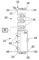
본 발명의 제1 실시예에 따른 제1 제어 회로(20)가 도 2에 도시된다. A
제1 제어 회로(20)는 제1 단자(22) 및 제2 단자(24)를 포함한다. 사용 시에, 제1 단자(22) 및 제2 단자(24)는 각각 +Vdc/2 및 -Vdc/2의 전압을 전달하는 제1 DC 전력 전송 라인(26) 및 제2 전력 전송 라인(28)에 연결된다. The
제1 제어 회로(20)는 제1 단자(22) 및 제2 단자(24) 사이에서 연장하는 전류 전송 경로를 더 포함한다. 전류 전송 경로는 제3 단자(34)에 의해 분리된 제1 전류 전송 경로부(30) 및 제2 전류 전송 경로부(32)를 갖는다. The first control circuit (20) further includes a current transmission path extending between the first terminal (22) and the second terminal (24). The current transmission path has a first current
제1 전류 전송 경로부(30)는 제1 단자(22)와 제3 단자(34) 사이에서 연장하고, 복수의 직렬-연결된 제1 모듈(36)을 포함한다. 각각의 제1 모듈(36)은 제1 커패시터의 형태의 에너지 저장 디바이스와 병렬로 연결된 두 쌍의 주 스위칭 요소(primary switching elements)를 포함한다. 두 쌍의 주 스위칭 요소 및 제1 커패시터는 풀-브리지(full-bridge) 구성으로 연결되어 영(zero), 음(negative) 또는 양(positive) 전압을 제공할 수 있고 두 방향으로 전류를 전도할 수 있는 4-상한 바이폴라 모듈(4-quadrant bipolar module)을 형성한다. The first current
제2 전류 전송 경로부(32)는 제2 단자(24) 및 제3 단자(34) 사이에서 연장하고 복수의 직렬-연결된 부 스위칭 요소(secondary switching element)(40)를 포함한다. The second current
각각의 스위칭 요소는 IGBT(Insulated Gate Bipolar Transistor) 형태의 반도체 디바이스로 구성된다. 각각의 스위칭 요소는 또한 그것과 병렬로 연결된 역-평행 다이오드(anti-parallel diode)를 포함한다. Each switching element is composed of a semiconductor device in the form of IGBT (Insulated Gate Bipolar Transistor). Each switching element also includes an anti-parallel diode connected in parallel with it.
제1 제어 회로(20)는 보조 단자(42)와, 제3 단자(34)와 보조 단자(42) 사이에서 연장하여 전류 전송 경로로부터 분기(branch)하는 에너지 변환 블록을 더 포함한다. 에너지 변환 블록은 제3 단자(34)와 보조 단자(42) 사이에 직렬로 연결된 덤프 저항(44)을 포함한다. 본 발명의 다른 실시예에서, 덤프 저항(44)이 복수의 덤프 저항으로 대체될 수 있음이 예상된다. The
사용 시에 보조 단자(42)는 DC 전력 전송 라인(28)에 연결된다. In use, the
제1 제어 회로(20)는 제어 유닛(46)을 더 포함하여 제1 전류 전송 경로부(30)로부터 각각의 제1 커패시터의 선택적 제거를 제어한다. 각각의 제1 커패시터는 다음과 같이 제1 전류 전송 경로부(30)로부터 선택적으로 제거된다. The
각각의 4-상한 바이폴라 모듈의 제1 커패시터는 주 스위칭 요소의 상태를 변경함으로써 선택적으로 바이패스(bypass)되거나 전류 전송 경로에 삽입된다. 각각의 4-상한 바이폴라 모듈이 영, 음 또는 양 전압을 제공하도록, 이는 선택적으로 전류를 제1 커패시터를 통하도록 하거나 전류가 제1 커패시터를 바이패스하도록 한다. The first capacitor of each 4-high limit bipolar module is selectively bypassed or inserted into the current transmission path by changing the state of the main switching element. Each of the four-upper limit bipolar modules provides zero, positive, or positive voltage, which selectively allows current to pass through the first capacitor or allows current to bypass the first capacitor.
각각의 4-상한 바이폴라 모듈의 주 스위칭 요소 쌍이 4-상한 바이폴라 모듈에 단락 회로를 형성하도록 구성되는 경우 각각의 4-상한 바이폴라 모듈의 제1 커패시터는 바이패스된다. 이는 제1 전류 전송 경로부(30)의 전류가 단락 회로를 통과하고 제1 커패시터를 바이패스하도록 하고, 따라서 4-상한 바이폴라 모듈이 영 전압을 제공, 즉, 4-상한 바이폴라 모듈이 바이패스 모드로 구성되어 제1 전류 전송 경로부(30)로부터 제거된다. When the main switching element pair of each 4-upper limit bipolar module is configured to form a short circuit to the 4-upper limit bipolar module, the first capacitor of each 4-upper limit bipolar module is bypassed. This allows the current in the first current
각각의 4-상한 바이폴라 모듈의 주 스위칭 요소 쌍이 제1 전류 전송 경로부(30)의 전류가 제1 커패시터로 유입되고 제1 커패시터로부터 유출되게 하도록 구성되는 경우 각각의 4-상한 바이폴라 모듈의 제1 커패시터가 제1 전류 전송 경로부(30)로 삽입된다. 제1 커패시터는 그 다음 영이 아닌 전압을 제공하기 위하여, 즉, 4-상한 바이폴라 모듈이 비-바이패스 모드(non-bypassed mode)로 구성되고 따라서 제1 전류 전송 경로부(30)로부터 제거되지 않도록 그것의 충전된 에너지를 방전하거나 충전한다. 4-상한 바이폴라 모듈의 양방향 특성은, 양 또는 음 전압을 제공하기 위하여 제1 커패시터가 순방향 또는 역방향으로 제1 전류 전송 경로부(30)로 삽입될 수 있음을 의미한다. If the main switching element pair of each 4-high limit bipolar module is configured to cause the current of the first current
각각 그 자신의 전압을 제공하는, 다수의 제1 모듈(36)의 제1 커패시터를 제1 전류 전송 경로부(30)에 삽입함으로써, 개개의 제1 모듈(36) 각각으로부터 이용가능한 전압보다 높은, 복수의 제1 모듈(36) 양단의 결합된 전압을 구축하는 것이 가능하다. 이러한 방식에서 각각의 제1 모듈(36)의 주 스위칭 요소의 스위칭은 복수의 제1 모듈(36)이 계단형(stepped) 가변 전압원을 제공하도록 하며, 이는 단계적 근사(step-wiseapproximation)를 이용하여 복수의 제1 모듈(36)에 걸쳐 전압 파형의 생성을 가능하게 한다. By inserting a first capacitor of a plurality of
본 발명의 다른 실시예에서, 각각의 제1 모듈은 양방향 전류 능력을 갖는 다른 방식으로 구성될 수 있음이 예상된다. 예를 들어, 각각의 제1 모듈은 하프-브리지 구성의 제1 커패시터에 병렬로 연결된 주 스위칭 요소 쌍을 포함하여 영 또는 양 전압을 제공하고 두 방향으로 전류를 전도할 수 있는 2-상한 유니폴라 모듈(2-quadrant unipolar module)을 형성할 수 있다.In another embodiment of the present invention, it is contemplated that each first module may be configured in other ways with bi-directional current capability. For example, each first module may include a pair of primary switching elements connected in parallel to a first capacitor of a half-bridge configuration to provide a zero-or-positive voltage and a two- Module (2-quadrant unipolar module).
제어 유닛(46)은 또한 복수의 부 스위칭 요소(40)의 스위칭을 제어한다. The
DC 전력 전송 방식 내에서의 제1 제어 회로(20)의 작동은 도 3을 참조하여 다음과 같이 설명된다. The operation of the
제1 DC 전력 전송 라인(26) 및 제2 DC 전력 전송 라인(28)은, 대응하는 제1 AC 네트워크 및 제2 AC 네트워크(도시되지 않음)의 각각의 상(phase)에 연결된 제1 전력 변환기(48) 및 제2 전력 변환기(50)를 상호연결한다. 전력은 대응하는 전력 변환기와 제1 및 제2 DC 전력 전송 라인(26, 28)을 통해 제1 AC 네트워크로부터 제2 AC 네트워크로 전송된다. The first DC
정상 작동 동안 제1 제어 회로(20)는 각각의 제1 모듈(36)의 제1 커패시터가 전류 전송 경로에 연결되는 대기 구성(standby configuration)을 채용한다. 한편 제어 유닛(46)은 각각의 부 스위칭 요소(40)를 온-상태로 스위칭하여 전류가 제2 전류 전송 경로부(32)를 통해 흘러서 덤프 저항(44)을 바이패스하도록 한다. 즉, 제2 전류 전송 경로부(32)는 덤프 저항(44)을 회로의 밖으로 "단락"하도록 구성되고 제1 제어 회로(20)가 대기 구성에 있는 동안 그 상태로 유지된다. 이러한 방식으로 제2 전류 전송 경로부(32)를 구성하는 목적은 덤프 저항(44)을 통한 에너지 소산을 통해 전력 손실을 최소화하는 것이다. During normal operation, the
제1 전류 전송 경로부(30) 양단의 총 전압은 DC 전력 전송 라인(26, 28) 양단의 전압인 VDC와 대략 동일하다. 대기 구성에서 영 또는 최소 전류가 전류 전송 경로를 통해 흐른다. The total voltage across the first current
예를 들어 제2 AC 네트워크에서의 장애(fault)의 결과로 제2 전력 변환기(50)가 전송된 전력을 수신할 수 없는 이벤트에서, 제1 AC 네트워크는 전력 전달이 영으로 감소할 수 있을 때까지 일시적으로 DC 전송 라인으로 전력 전송을 계속해야 하는데, 풍력 발전 설비의 경우 통상적으로 1-2초가 걸린다. 이것은 DC 전력 전송 라인(26, 28)에서의 초과 에너지 축적으로 이어질 수 있다. DC 전력 전송 라인(26, 28)으로부터의 초과 에너지의 제거는 DC 전력 전송 라인(26, 28)을 과전압으로부터 보호하고 필요한 경우 저전압 장애 보상(ride-through)을 보장하기 위하여 필요하다. For example, in an event where the
제1 AC 네트워크가 제1 전력 변환기(48)를 통해 DC 전송 라인으로 전력을 계속하여 전송하도록 하기 위하여, 제어 유닛(46)은 각각의 부 스위칭 요소(40)를 오프-상태로 선택적으로 스위칭하여 제2 전류 전송 경로부(32)를 통해 흐르는 전류를 차단하고 따라서 전류가 덤프 저항(44)으로 향하도록 한다. 한편, 제어 유닛(46)은 각각의 제1 커패시터를 제1 전류 전송 경로부(30)로부터 선택적으로 제거하여 제1 전류 전송 경로부(30) 양단에 전압 파형(V1)을 생성하는데, 이러한 전압 파형은 유한한 전압 단계를 DC 전송 라인 양단의 전압(VDC)에 가산하거나 감산한다. 이것은 전류(Idump)가 DC 전력 전송 라인(26, 28)으로부터 제1 전류 전송 경로부(30)를 통해 덤프 저항(44)으로 흐르도록 하고, 따라서 DC 전력 전송 라인(26, 28)으로부터 초과 에너지를 제거하기 위해 덤프 저항(44)을 통한 에너지 소산을 가능하게 한다. In order to allow the first AC network to continuously transmit power to the DC transmission line through the
에너지 제거 모드에서, 제1 제어 회로(20)는 비교적 높은 전류(통상적으로 유닛당 1.0)를 DC 전력 전송 라인(26, 28)으로부터 인출하고 DC 전력 전송 라인(26, 28)과 실제 전력을 교환한다. In the energy removal mode, the
이러한 방식에서 제1 제어 회로(20)는 에너지 제거 디바이스로서 사용되어 DC 전력 전송 라인(26, 28)으로부터 초과 에너지를 제거할 수 있다. In this manner, the
제1 제어 회로(20)가 복수의 제1 모듈(36)을 포함함으로써 광범위한 전압 파형의 생성을 가능하게 하여, DC 전력 전송 라인(26, 28)으로부터 제거될 초과 에너지에 대응하도록 덤프 저항(44)을 통해 흐르는 전류를 능동적으로 수정한다. The
전류 전송 경로로부터 각각의 제1 커패시터를 선택적으로 제거하는 능력은 DC 전력 전송 라인(26, 28)으로부터 제1 제어 회로(20)로의 에너지, 즉, 초과 전력의 빠른 전달을 허용하여 DC 전력 전송 라인(26, 28)에서의 에너지 레벨의 신속한 조절을 가능하게 하는 것으로 밝혀졌다. 이것은 결국 연관된 전기 네트워크에서의 장애 이벤트 시에 DC 전력 전송 라인(26, 28)의 에너지 레벨을 조절하기 위한 요구에 제1 제어 회로(20)가 신속하게 응답할 수 있도록 한다. The ability to selectively remove each first capacitor from the current transfer path allows for rapid transfer of energy from the DC
또한, 보조 단자(42)의 제2 DC 전력 전송 라인(28)에 대한 연결은 결국 덤프 저항(44)이 접지가 아닌, 제2 DC 전력 전송 라인(28)에 연결되도록 하고 따라서 고전류가 DC 전력 전송 라인(26, 28)의 부유 커패시턴스(stray capacitance) 대신에 DC 전력 전송 라인(26, 28)을 통해 순환하도록 한다. In addition, the connection of the
제2 전류 전송 경로부(32)는 대기 구성 및 에너지 제거 모드에서 영 또는 영이 아닌 전류를 전도하는 것이 이해될 것이다. 이것은 따라서 제2 전류 전송 경로부(32)에서의 저전류, 고전압 반도체 디바이스의 사용을 허용하고, 결국 손실, 비용 및 풋프린트(footprint)의 측면에서 감소를 제공한다. It will be understood that the second current
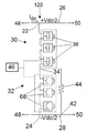
본 발명의 제2 실시예에 따른 제2 제어 회로(120)가 도 4에 도시된다. 도 4에 도시된 제2 제어 회로(120)는 구조 및 작동에 있어서 도 1에 도시된 제1 제어 회로(20)와 유사하고, 유사한 구성은 동일한 도면부호를 공유한다. A
제2 제어 회로(120)는, 제2 제어 회로(120)에서 복수의 직렬-연결된 부 스위칭 요소(40)가 복수의 직렬-연결된 제2 모듈(68)로 대체된다는 점에서 제1 제어 회로(20)와 상이하다. 각각의 제2 모듈(68)은 제2 커패시터 형태의 에너지 저장 디바이스와 병렬 연결된 주 스위칭 요소 쌍을 포함한다. 주 스위칭 요소 쌍과 제2 커패시터는 하프-브리지 구성으로 연결되어 영 또는 양 전압을 제공하고 두 방향으로 전류를 전도할 수 있는 2-상한 유니폴라 모듈을 형성한다. The
사용 시에, 제어 유닛(46)은 제2 전류 전송 경로부(32)로부터의 각각의 제2 커패시터의 선택적 제거를 제어한다. 각각의 제2 커패시터는 다음과 같이 제2 전류 전송 경로부(32)로부터 선택적으로 제거 가능하다. In use, the
각각의 2-상한 유니폴라 모듈의 제2 커패시터는 주 스위칭 요소의 상태를 변경함으로써 선택적으로 바이패스되거나 전류 전송 경로에 삽입된다. 이는, 각각의 2-상한 유니폴라 모듈이 영 또는 양 전압을 제공하도록, 선택적으로 전류가 제2 커패시터를 통하도록 하거나 또는 전류가 제2 커패시터를 바이패스하도록 한다. The second capacitor of each two-high limit unipolar module is selectively bypassed or inserted into the current transmission path by changing the state of the main switching element. This allows either the two-high-limit unipolar module to provide zero or positive voltage, optionally allowing current to pass through the second capacitor, or allowing current to bypass the second capacitor.
각각의 2-상한 유니폴라 모듈의 주 스위칭 요소 쌍이 2-상한 유니폴라 모듈에 단락 회로를 형성하도록 구성되는 경우 각각의 2-상한 유니폴라 모듈의 제2 커패시터는 바이패스된다. 이것은 제2 전류 전송 경로부(32)의 전류가 단락 회로를 통과하고 제2 커패시터를 바이패스하도록 하고, 따라서 2-상한 유니폴라 모듈은 영 전압을 제공, 즉, 2-상한 유니폴라 모듈은 바이패스 모드로 구성되고 이에 따라 제2 전류 전송 경로부(32)로부터 제거된다. When the main switching element pair of each two-high limit unipolar module is configured to form a short circuit to the two-high limit unipolar module, the second capacitor of each two-high limit unipolar module is bypassed. This allows the current in the second current
각각의 2-상한 유니폴라 모듈의 주 스위칭 요소 쌍이 제2 전류 전송 경로부(32)의 전류가 제2 커패시터로 유입되고 제2 커패시터로부터 유출되게 하도록 구성되는 경우 각각의 2-상한 유니폴라 모듈의 제2 커패시터는 제2 전류 전송 경로부(32)에 삽입된다. 제2 커패시터는 그 다음 영이 아닌 전압을 제공하기 위하여, 즉, 2-상한 유니폴라 모듈이 비-바이패스 모드로 구성되고 따라서 제2 전류 전송 경로부(32)로부터 제거되지 않도록 하기 위하여, 그것의 저장된 에너지를 방전하거나 충전한다. And the pair of main switching elements of each 2-high limit unipolar module is configured to cause the current of the second current
복수의 제1 모듈(36)과 관련하여 앞서 설명한 바와 동일한 방식으로 복수의 제2 모듈(68) 양단의 결합된 전압을 구축하는 것이 가능하다. It is possible to construct a combined voltage across the plurality of
제2 제어 회로(120)의 작동은 다음을 제외하고는 제1 제어 회로(20)의 작동과 유사하다: DC 전력 전송 라인(26, 28)으로부터 에너지를 제거하는 경우, 제어 유닛(46)은 제2 전류 전송 경로부(32)의 각각의 제2 모듈(68)의 주 스위칭 요소의 상태를 선택적으로 스위칭하여 제2 전류 전송 경로부(32)를 통해 흐르는 전류를 차단하거나 최소화하고 따라서 전류가 덤프 저항(44)으로 향하도록 한다. The operation of the
바람직하게 제2 제어 회로(120)는, DC 전력 전송 라인(26, 28)으로부터 에너지를 제거하는 동안 제2 전류 전송 경로부(32)를 통해 흐르는 전류가 영이 되도록 제어되어야 한다. 그러나, 실제로, 일부 전류가 제2 전류 전송 경로부(32)를 통해 흘러서 제2 커패시터의 충전 및 방전이 덤프 저항(44) 양단의 원하는 전압을 달성할 수 있도록 할 것이다. Preferably, the
손실, 비용 및 풋프린트 측면에서의 감소를 제공하도록 각각의 복수의 제2 모듈(68)이 각각의 복수의 제1 모듈(36)보다 낮은 정격(rating)을 갖도록 구성될 수 있음이 이해될 것이다. 이것은, 제1 제어 회로(20)와 관련하여 앞서 기재된 바와 같이, 제2 전류 전송 경로부(32)가 대기 구성 및 에너지 제거 모드에서 영 또는 영이 아닌 전류를 전도하기 때문이다. It will be appreciated that each of the plurality of
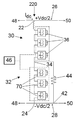
본 발명의 제3 실시예에 따른 제3 제어 회로(220)가 도 5에 도시된다. 도 5에 도시된 제3 제어 회로(220)는 도 4에 도시된 제2 제어 회로(120)와 구조 및 작동에 있어서 유사하고, 유사한 구성은 동일한 도면부호를 공유한다. A
제3 제어 회로(220)는, 제3 제어 회로(220)에서 각각의 제2 모듈(70)이 제2 커패시터 형태의 에너지 저장 디바이스와 병렬 연결된 두 쌍의 주 스위칭 요소를 포함한다는 점에서 제2 제어 회로(120)와 상이하다. 주 스위칭 요소 쌍과 제2 커패시터는 풀-브리지 구성으로 연결되어 영, 음 또는 양 전압을 제공하고 두 방향으로 전류를 전도할 수 있는 4-상한 바이폴라 모듈을 형성한다. The
사용 시에, 제어 유닛(46)은 제2 전류 전송 경로부(32)로부터의 각각의 제2 커패시터의 선택적 제거를 제어한다. 각각의 제2 커패시터는, 제1 제어 회로(20)에서의 제1 전류 전송 경로부(30)로부터의 각각의 제1 모듈(36)의 선택적 제거와 동일한 방식으로 제2 전류 전송 경로부(32)로부터 선택적으로 제거 가능하다. In use, the
제2 전류 전송 경로부(32)에서 2-상한 유니폴라 모듈 대신에 4-상한 바이폴라 모듈을 사용하는 것 외에는, 제3 제어 회로(220)의 작동은 제2 제어 회로(120)의 작동과 유사하다. The operation of the
제2 전류 전송 경로부(32)에서의 4-상한 바이폴라 모듈의 사용은, 그것이 전송 전력의 방향이 바뀌는 경우 DC 전압의 극성이 변경되는 LCC HVDC 방식과 결합하여 제3 제어 회로(220)의 사용을 가능하게 한다는 점에서 유용하다. The use of the 4-high-limit bipolar module in the second current
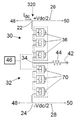
본 발명의 제4 실시예에 따른 제4 제어 회로(320)가 도 6에 도시된다. 도 6에 도시된 제4 제어 회로(320)는 구조 및 작동에 있어서 도 5에 도시된 제3 제어 회로(220)와 유사하고, 유사한 구성은 동일한 도면부호를 공유한다. A
제4 제어 회로(320)는, 사용 시에 보조 단자(42)가 제2 DC 전송 라인(28) 대신에 접지에 연결되고 제2 전류 전송 경로부(32)가 복수의 제2 모듈(70)과 직렬 연결된 제2 인덕터를 더 포함한다는 점에서 제3 제어 회로(220)와 상이하다. The
DC 전력 전송 방식에서의 제4 제어 회로(320)의 작동이 도 7을 참조하여 다음과 같이 설명된다. The operation of the
제1 DC 전력 전송 라인(26) 및 제2 DC 전력 전송 라인(28)은 대응하는 제1 AC 네트워크 및 제2 AC 네트워크(도시되지 않음)의 각각의 상에 연결된 제1 전력 변환기(48) 및 제2 전력 변환기(50)를 상호연결한다. 전력은 대응하는 전력 변환기와 제1 및 제2 DC 전력 전송 라인(26, 28)을 통해 제1 AC 네트워크로부터 제2 AC 네트워크로 전송된다. The first DC
정상 작동 동안 제4 제어 회로(320)는 제1 모듈 및 제2 모듈(70)의 커패시터가 전류 전송 경로에 연결되는 대기 구성을 채용한다. 한편 제1 전류 전송 경로부(30) 및 제2 전류 전송 경로부(32)는, 제4 제어 회로(320)가 대기 구성인 경우 덤프 저항(44)을 통해 흐르는 전류를 차단 또는 최소화하고 이에 따라 덤프 저항(44)을 통한 에너지 소산을 최소화하기 위하여 덤프 저항(44) 양단에 영 또는 영이 아닌 전압을 유지하도록 구성된다. 이러한 방식으로 제1 전류 전송 경로부(30) 및 제2 전류 전송 경로부(32)를 구성하는 목적은 덤프 저항(44)을 통한 에너지 소산을 통한 전력 손실을 최소화하는 것이다. During normal operation, the
제1 전류 전송 경로부(30) 양단의 총 전압은 DC 전력 전송 라인(26, 28) 양단의 전압인 VDC와 대략 동일하다. 대기 구성에서 전류 전송 경로를 통해 영 또는 최소 전류가 흐른다. The total voltage across the first current
제2 전력 변환기(50)가 예를 들어 제2 AC 네트워크에서의 장애의 결과로 전송 전력을 수신할 수 없는 이벤트에서, 제1 AC 네트워크는 전력 전달이 영으로 감소될 수 있을 때까지 DC 전송 라인으로 일시적으로 전력 전송을 계속해야 하는데, 풍력 발전 설비의 경우 통상적으로 1-2초가 걸린다. 앞서 설명된 바와 같이, 이는 DC 전력 전송 라인(26, 28)에서의 초과 에너지 축적으로 이어질 수 있다. DC 전력 전송 라인(26, 28)으로부터의 초과 에너지의 제거는 DC 전력 전송 라인(26, 28)을 과전압으로부터 보호하고 필요한 경우 저전압 장애 보상을 보장하기 위하여 필요하다. In an event where the
제1 AC 네트워크가 제1 전력 변환기(48)를 통해 DC 전송 라인으로 전력 전송을 계속하도록 하기 위하여, 제어 유닛(46)은 각각의 제1 커패시터 및 제2 커패시터를 제1 전류 전송 경로부(30) 및 제2 전류 전송 경로부(32)로부터 선택적으로 제거하여 제1 전류 전송 경로부(30) 및 제2 전류 전송 경로부(32) 각각의 양단에 전압 파형을 생성하는데, 이러한 전압 파형은 DC 전송 라인 양단의 전압(VDC)에 유한한 전압 단계를 가산하거나 감산한다. 제1 전류 전송 경로부(30) 및 제2 전류 전송 경로부(32) 양단의 전압 파형은 덤프 저항(44) 양단에 AC 전압 파형을 생성하도록 형상화된다. 이는 전류(IAC _ dump/2)가 DC 전력 전송 라인(26, 28)으로부터 제1 전류 전송 경로부(30) 및 제2 전류 전송 경로부(32)를 통해 흐르도록 하고 전류(IAC _ dump)가 덤프 저항(44)으로 흐르도록 하며, 이에 따라 DC 전력 전송 라인(26, 28)으로부터 초과 에너지를 제거하기 위하여 덤프 저항(44)을 통한 에너지 소산을 가능하게 한다. In order to allow the first AC network to continue transmitting power to the DC transmission line through the
제4 제어 회로(320)의 시뮬레이션 모델이 Matlab-Simulink를 이용하여 구현되어 그 작동을 도시하였다. 시뮬레이션 모델의 표현(representation)은 도 8에 도시되며, 여기서 각각의 제1 커패시터 및 제2 커패시터가 DC 전압원으로서 모델링되고 제4 제어 회로(320)가 DC 전압원과 병렬 연결된다. The simulation model of the
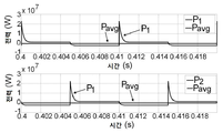
사각 전압 파형 수요전력(square voltage waveform demand)이 제1 전류 전송 경로부(30) 및 제2 전류 전송 경로부(32) 각각에 대해 설정된다. 제1 전류 전송 경로부(30) 및 제2 전류 전송 경로부(32) 각각에 대해 각각의 사각 전압 파형 수요전력의 양의 피크는 Vdc로 설정되고, 반면 제1 전류 전송 경로부(30) 및 제2 전류 전송 경로부(32) 각각에 대해 각각의 사각 전압 파형 수요전력의 음의 피크는, 복수의 제1 모듈(36)에 걸친 전력(P1) 변화와 영인(nil) 평균 전력(Pavg)에 의해 나타내어지는 영의 순 에너지 교환(zero net energy exchange)을 그래프 형태로 나타내는 도 9a에 도시된 바와 같이, 단일 사이클에 대해 순 에너지 교환이 영이 되도록 제1 커패시터 및 제2 커패시터에서 손실된 임의의 에너지를 재저장하기 위하여 비례-적분 조절기(proportional-integral regulator)에 의해 제어되는 음의 전압값이다. A square voltage waveform demand is set for each of the first current
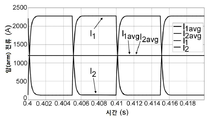
실제로, 생성된 전압 파형의 음의 값은 일정한 DC 전류가 전류 전송 경로를 통해 제2 DC 전력 전송 라인(28)으로부터 제1 DC 전력 전송 라인(26)으로 흐르도록 하여 제1 커패시터 및 제2 커패시터로부터 덤프 저항(44)으로의 임의의 에너지 손실을 보상한다. 제1 전류 전송 경로부(30)에서의 순시 전류(I1) 및 영 평균 전류(I1avg)와 제2 전류 전송 경로부(32)에서의 순시 전류(I2) 및 영 평균 전류(I2avg)를 그래프 형태로 나타내는 도 9b에 도시된 바와 같이, 일정한 DC 전류는 전류 전송 경로를 통해 덤프 저항(44)으로 흐르는 AC 전류를 상쇄(offset)한다. In fact, the negative value of the generated voltage waveform causes a constant DC current to flow from the second DC
도 9c는 덤프 저항(44)에서 소모되는 평균 전력(PRavg) 및 순시 전력(PR)을 그래프 형태로 도시한다. Figure 9C shows the average power (P Ravg ) and instantaneous power (P R ) consumed in the dump resistor (44) in graphical form.
제1 전류 전송 경로부(30) 및 제2 전류 전송 경로부(32) 각각의 양단에 180° 위상 변이된 사각 전압 파형을 사용함으로써 제1 커패시터 및 제2 커패시터를 통하는 전류의 피크 값을 감소시킬 뿐만 아니라 복수의 제1 모듈(36) 및 복수의 제2 모듈(70) 각각에 대해 단일 사이클에서 영의 순 에너지 교환의 결과를 낳는다는 것이 시뮬레이션 모델로부터 밝혀졌다. 따라서 제1 전류 전송 경로부(30) 및 제2 전류 전송 경로부(32) 각각의 양단에 180° 위상 변이된 사각 전압 파형을 사용한 결과 DC 전력 전송 라인(26, 28)으로부터의 에너지 제거 동안 제4 제어 회로(320)가 안정적으로 작동한다. The peak value of the current passing through the first capacitor and the second capacitor is reduced by using a rectangular voltage waveform that is 180 ° out of phase with respect to each of the first current
본 발명의 제5 실시예에 따른 제5 제어 회로(420)가 도 10에 도시된다. 도 10에 도시된 제5 제어 회로(420)는 도 4에 도시된 제2 제어 회로(120)와 구조에 있어서 유사하며, 유사한 구성은 동일한 도면부호를 공유한다. A
제5 제어 회로(420)는, 제5 제어 회로(420)가 복수의 제1 모듈(36)을 생략하고 에너지 변환 블록이 덤프 저항(44)에 직렬로 연결된 복수의 직렬-연결된 보조 스위칭 요소(100)를 더 포함한다는 점에서 제2 제어 회로(120)와 상이하다. The
DC 전력 전송 방식에서의 제5 제어 회로(420)의 작동이 다음과 같이 설명된다. The operation of the
정상 작동 동안 제5 제어 회로(420)는 각각의 제2 커패시터가 전류 전송 경로에 연결되는 대기 구성을 채용한다. 한편 각각의 보조 스위칭 요소(100)는 오프-상태로 스위칭되어 덤프 저항(44)에서의 전류 흐름을 억제하여 에너지 손실을 최소화한다. During normal operation, the
DC 전력 전송 라인(26, 28)으로부터 에너지를 제거하기 위하여, 각각의 스위칭 요소(100)는 온-상태로 스위칭되어 덤프 저항(44)에서의 전류 흐름을 허용한다. 이 단계에서 제어 유닛(46)은 각각의 제2 커패시터를 제2 전류 전송 경로부로부터 선택적으로 제거하여, 각각의 보조 스위칭 요소(100)가 온-상태로 스위칭되는 경우 각각의 보조 스위칭 요소(100)의 소프트-스위칭이 가능하도록 제3 단자(34)에서의 전압을 수정한다. In order to remove energy from the DC
각각의 보조 스위칭 요소(100)의 온-상태로의 스위칭은 DC 전류가 DC 전력 전송 라인(26, 28)으로부터 전류 전송 경로를 통하여 덤프 저항(44)으로 흐르도록 한다. 이는 DC 전력 전송 라인(26, 28)으로부터의 초과 에너지를 제거하기 위하여 덤프 저항(44)을 통한 에너지 소산을 허용한다. The switching of each of the
DC 전력 전송 라인(26, 28)이 정상 작동을 재개하고 제5 제어 회로(420)가 더 이상 DC 전력 전송 라인(26, 28)으로부터 에너지를 제거하도록 작동할 필요가 없어진 후에, 제5 제어 회로(420)가 그 대기 구성으로 재구성되기 전에 각각의 보조 스위칭 요소(100)는 오프-상태로 다시 스위칭되어 덤프 저항(44)에서의 전류 흐름을 억제한다. 이 단계에서 제어 유닛(46)은 제2 전류 전송 경로부로부터 각각의 제2 커패시터를 선택적으로 제거하여, 각각의 보조 스위칭 요소(100)가 다시 오프-상태로 스위칭되는 경우 각각의 보조 스위칭 요소(100)의 소프트-스위칭이 가능하도록 제3 단자(34)에서의 전압을 수정한다. After the DC
이러한 방식에서 제5 제어 회로(420)는 또한 DC 전력 전송 라인(26, 28)으로부터 에너지를 제거할 수 있는 더욱 간단한 구성을 제공한다. In this manner, the
제2 전류 전송 경로부(32)가 손실, 비용 및 풋프린트 측면에세의 감소를 제공하기 위하여 복수의 직렬-연결된 보조 스위칭 요소(100)보다 낮은 정격을 갖도록 구성될 수 있음이 이해될 것이다. 이는 전류 전송 경로로부터 각각의 제2 커패시터를 선택적으로 제거하는 것이 DC 전력 전송 라인(26, 28)으로부터의 에너지 제거를 제어하는데 필수적이지 않기 때문이다. It will be appreciated that the second current
본 발명의 다른 실시예에서, 각각의 보조 스위칭 요소가 덤프 저항에서의 전류 흐름을 제어하기 위하여 보조 모듈로 대체될 수 있고 이러한 보조 모듈은 각각 적어도 하나의 보조 에너지 저장 디바이스를 포함할 수 있다는 것이 예상된다. 바람직하게 각각의 보조 모듈은 적어도 하나의 보조 스위칭 요소를 포함하여 선택적으로 전류를 이러한 보조 에너지 저장 디바이스 또는 각각의 보조 에너지 저장 디바이스를 통하도록 하거나 또는 선택적으로 전류가 이러한 보조 에너지 저장 디바이스 또는 각각의 보조 에너지 저장 디바이스를 바이패스하도록 한다. In another embodiment of the present invention, it is contemplated that each auxiliary switching element may be replaced with an auxiliary module to control the flow of current in the dump resistor and each such auxiliary module may include at least one auxiliary energy storage device do. Preferably each auxiliary module comprises at least one auxiliary switching element to selectively allow current to flow through the auxiliary energy storage device or each auxiliary energy storage device or alternatively to allow current to flow through the auxiliary energy storage device or each auxiliary Thereby bypassing the energy storage device.
각각의 보조 모듈은 양방향 전류 능력을 갖도록 구성될 수 있다. 예를 들어, 각각의 보조 모듈은, 앞선 실시예에서 위에 명시된 바와 같이 전류 전송 경로의 제1 모듈 및 제2 모듈에서와 동일한 방식으로 양방향 전류 능력을 갖도록 구성될 수 있다. Each auxiliary module may be configured to have bi-directional current capability. For example, each auxiliary module may be configured to have bi-directional current capability in the same manner as in the first and second modules of the current transmission path, as specified above in the previous embodiment.
각각의 보조 스위칭 요소는 또한 선택적으로 단방향 전류 능력을 갖도록 구성된, 즉, 그 보조 에너지 저장 디바이스 또는 각각의 보조 에너지 저장 디바이스가 단 하나의 방향으로 전류를 전도할 수 있도록 구성된, 보조 모듈에 의해 대체될 수 있다. 예를 들어, 각각의 보조 모듈은 직렬-연결된 전류 흐름 제어 요소의 제1 세트 및 제2 세트를 포함할 수 있고, 각각의 직렬-연결된 전류 흐름 제어 요소 세트는 전류를 그 보조 에너지 저장 디바이스 또는 각각의 보조 에너지 저장 디바이스로 향하게 하기 위한 능동 스위칭 요소와 보조 모듈을 통하는 전류 흐름을 단일 방향으로 제한하기 위한 수동 전류 체크 요소를 포함하며, 직렬-연결된 전류 흐름 제어 요소의 제1 및 제2 세트와 그 보조 에너지 저장 디바이스 또는 각각의 보조 에너지 저장 디바이스는 풀-브리지 구성으로 배치되어 단일 방향으로 전류를 전도하면서 영, 양 또는 음 전압을 제공할 수 있는 합리화된 2-상한 바이폴라 모듈(2-quadrant bipolar rationalised module)을 형성한다. Each auxiliary switching element may also be replaced by an auxiliary module configured to have unidirectional current capability, i. E., The auxiliary energy storage device or each auxiliary energy storage device is configured to conduct current in only one direction . For example, each auxiliary module may comprise a first set and a second set of series-connected current flow control elements, each set of series-connected current flow control elements supplying current to its auxiliary energy storage device or And a passive current check element for limiting the current flow in a single direction through the auxiliary module, wherein the first and second sets of series-connected current flow control elements and the first and second sets of series- The auxiliary energy storage device or each auxiliary energy storage device may be a rationalized two-quadrant bipolar rationalised (BIP) module capable of providing zero, positive or negative voltages while being placed in a full-bridge configuration to conduct current in a single direction module.
본 발명의 다른 실시예에서(도시되지 않음), 스위칭 요소 중 하나 이상은 예컨대, 게이트 턴 오프 사이리스터(gate turn-off thyristor), FET(field effect transistor), IEGT(injection-enhanced gate transistor), 통합 게이터 정류 사이리스터(integrated gate commutated thyristor)와 같은 상이한 스위칭 디바이스 또는 임의의 기타 자가-정류 반도체 디바이스(self-commutated semiconductor device)일 수 있음이 예상된다. 각각의 예에서, 스위칭 디바이스는 역-평행 다이오드와 병렬 연결된다. In another embodiment of the present invention (not shown), one or more of the switching elements may be a gate turn-off thyristor, a field effect transistor (FET), an injection-enhanced gate transistor (IEGT) It is anticipated that it may be a different switching device such as an integrated gate commutated thyristor or any other self-commutated semiconductor device. In each example, the switching device is connected in parallel with the anti-parallel diode.
본 발명의 다른 실시예에서(도시되지 않음), 각각의 모듈의 커패시터는 예컨대, 연료 전지, 배터리 또는 전기 에너지를 저장 및 방출하여 전압을 제공할 수 있는 임의의 기타 에너지 저장 디바이스와 같은 상이한 에너지 저장 디바이스로 대체될 수 있음이 예상된다. In another embodiment of the present invention (not shown), the capacitors of each module may be a different energy storage device such as, for example, a fuel cell, a battery, or any other energy storage device capable of storing and discharging electrical energy to provide a voltage Devices. ≪ / RTI >
Claims (18)
상기 제1 단자와 상기 제2 단자 사이에서 연장하고 제3 단자에 의해 분리되는 제1 전류 전송 경로부 및 제2 전류 전송 경로부를 갖는 전류 전송 경로로서, 상기 제1 전류 전송 경로부 및 상기 제2 전류 전송 경로부 중 하나 또는 양자 모두는 하나 이상의 모듈을 포함하고, 상기 모듈 또는 각각의 모듈은 하나 이상의 에너지 저장 디바이스를 포함하는, 전류 전송 경로;
접지 또는 상기 제2 전력 전송 라인에의 연결을 위한 보조 단자;
상기 전력 전송 라인으로부터 에너지를 제거하기 위한 에너지 변환 블록으로서, 상기 에너지 변환 블록은, 상기 제3 단자와 상기 보조 단자 사이에서 연장하여 상기 전류 전송 경로로부터 분기하고 하나 이상의 에너지 변환 요소를 포함하는, 에너지 변환 블록; 및
상기 에너지 저장 디바이스 또는 각각의 에너지 저장 디바이스를 상기 전류 전송 경로로부터 선택적으로 제거하는 제어 유닛을 포함하는 제어 회로.A first terminal and a second terminal for respectively connecting to the first power transmission line and the second power transmission line;
A current transmission path having a first current transmission path portion extending between the first terminal and the second terminal and separated by a third terminal and a second current transmission path portion, One or both of the current transmission path portions include one or more modules, and wherein the or each module includes one or more energy storage devices;
An auxiliary terminal for grounding or connection to the second power transmission line;
An energy conversion block for removing energy from the power transmission line, the energy conversion block comprising: an energy conversion block that extends between the third terminal and the auxiliary terminal and branches from the current transmission path and includes one or more energy conversion elements Conversion block; And
And a control unit for selectively removing the energy storage device or each energy storage device from the current transmission path.
상기 제어 유닛은, 상기 에너지 저장 디바이스 또는 각각의 에너지 저장 디바이스를 상기 전류 전송 경로로부터 선택적으로 제거하여, 상기 전력 전송 라인으로부터 에너지를 제거하기 위해 전류가 상기 전력 전송 라인으로부터 상기 전류 전송 경로를 통하여 상기 에너지 변환 요소 또는 각각의 에너지 변환 요소로 흐르도록 하는, 제어 회로.The method according to claim 1,
Wherein the control unit is operable to selectively remove the energy storage device or each energy storage device from the current transmission path to cause current to flow from the power transmission line through the current transmission path To the energy conversion element or to each energy conversion element.
상기 제1 전류 전송 경로부는, 하나 이상의 제1 모듈을 포함하고, 상기 제1 모듈 또는 각각의 제1 모듈은 하나 이상의 제1 에너지 저장 디바이스를 포함하는, 제어 회로.3. The method according to claim 1 or 2,
Wherein the first current transmission path portion comprises at least one first module and wherein the first module or each first module comprises at least one first energy storage device.
상기 하나 이상의 제1 모듈은, 하나 이상의 주 스위칭 요소를 포함하여 선택적으로 전류가 상기 제1 에너지 저장 디바이스 또는 각각의 제1 에너지 저장 디바이스를 통하도록 하거나 또는 전류가 상기 제1 에너지 저장 디바이스 또는 각각의 제1 에너지 저장 디바이스를 바이패스하도록 하는, 제어 회로.The method of claim 3,
Wherein the at least one first module includes at least one primary switching element to selectively cause current to flow through the first energy storage device or each first energy storage device, And to bypass the first energy storage device.
상기 제2 전류 전송 경로부는, 상기 제2 전류 전송 경로부에서의 전류 흐름을 선택적으로 허용 또는 억제하도록 스위칭 가능한 하나 이상의 주 스위칭 블록을 포함하는, 제어 회로.5. The method according to any one of claims 1 to 4,
Wherein the second current transmission path section includes at least one main switching block switchable to selectively allow or suppress current flow in the second current transmission path section.
상기 하나 이상의 주 스위칭 블록은 하나 이상의 부 스위칭 요소를 포함하는, 제어 회로.6. The method of claim 5,
Wherein the at least one main switching block comprises at least one sub-switching element.
상기 하나 이상의 주 스위칭 블록은 제2 모듈을 포함하고,
상기 제2 모듈은 하나 이상의 제2 에너지 저장 디바이스를 포함하는, 제어 회로.The method according to claim 5 or 6,
Wherein the at least one main switching block comprises a second module,
Wherein the second module comprises at least one second energy storage device.
상기 하나 이상의 제2 모듈은, 하나 이상의 주 스위칭 요소를 포함하여 선택적으로 전류가 상기 제2 에너지 저장 디바이스 또는 각각의 제2 에너지 저장 디바이스를 통하도록 하거나 또는 전류가 상기 제2 에너지 저장 디바이스 또는 각각의 제2 에너지 저장 디바이스를 바이패스하도록 하는, 제어 회로.8. The method of claim 7,
Wherein the one or more second modules include one or more primary switching elements to selectively cause current to flow through the second energy storage device or each second energy storage device, And to bypass the second energy storage device.
상기 제어 유닛은, 선택적으로 상기 주 스위칭 블록 또는 각각의 주 스위칭 블록을 스위칭하여 상기 제2 전류 전송 경로부에서의 전류를 차단 또는 최소화함으로써 전류가 상기 에너지 변환 요소 또는 각각의 에너지 변환 요소로 향하도록 하는, 제어 회로.9. The method according to any one of claims 5 to 8,
Wherein the control unit selectively switches the main switching block or each main switching block to block or minimize the current in the second current transmission path portion so that current is directed to the energy converting element or each energy converting element Control circuit.
제6항에 따르는 경우, 상기 제어 유닛은, 상기 부 스위칭 요소 또는 각각의 부 스위칭 요소를 오프-상태로 선택적으로 스위칭하여 상기 제2 전류 전송 경로부에서의 전류를 차단함으로써 전류가 상기 에너지 변환 요소 또는 각각의 에너지 변환 요소로 향하도록 하는, 제어 회로.10. The method of claim 9,
The control unit according to claim 6, wherein the control unit selectively switches the sub-switching element or each sub-switching element to the off-state to interrupt the current in the second current- Or to each energy conversion element.
제8항에 따르는 경우, 상기 제어 유닛은, 상기 제2 모듈 또는 각각의 제2 모듈의 상기 주 스위칭 요소 또는 각각의 주 스위칭 요소를 선택적으로 스위칭하여 상기 제2 전류 전송 경로부에서의 전류를 차단 또는 최소화함에 따라 전류가 상기 에너지 변환 요소 또는 각각의 에너지 변환 요소로 향하도록 하는, 제어 회로.10. The method of claim 9,
The control unit according to claim 8, wherein the control unit selectively switches the main switching element or each main switching element of the second module or each second module to block current in the second current transmission path part Or minimizes the current to the energy conversion element or to each energy conversion element.
제3항 또는 제4항에 따르는 경우, 상기 제어 유닛은, 상기 제1 전류 전송 경로부 및 상기 제2 전류 전송 경로부로부터 각각의 에너지 저장 디바이스를 선택적으로 제거하여, 상기 전력 전송 라인으로부터 에너지를 제거하기 위해 상기 에너지 변환 요소 또는 각각의 에너지 변환 요소 양단에 AC 전압 파형을 생성하는, 제어 회로.9. The method according to claim 7 or 8,
The control unit according to claim 3 or 4, wherein the control unit selectively removes each energy storage device from the first current transmission path part and the second current transmission path part, And generates an AC voltage waveform across the energy conversion element or each energy conversion element for removal.
상기 제어 유닛은, 상기 제1 전류 전송 경로부 및 상기 제2 전류 전송 경로부로부터 각각의 에너지 저장 디바이스를 선택적으로 제거하여, 상기 제1 전류 전송 경로부 및 상기 제2 전류 전송 경로부 각각의 양단에 사각 전압 파형을 생성함으로써 상기 전력 전송 라인으로부터 에너지를 제거하기 위해 상기 에너지 변환 요소 또는 각각의 에너지 변환 요소 양단에 AC 전압 파형을 생성하는, 제어 회로.13. The method of claim 12,
Wherein the control unit selectively removes each of the energy storage devices from the first current transmission path portion and the second current transmission path portion to electrically connect both ends of each of the first current transmission path portion and the second current transmission path portion To generate an AC voltage waveform across the energy conversion element or each energy conversion element to remove energy from the power transmission line by generating a square voltage waveform on the energy conversion element.
상기 에너지 변환 블록은, 상기 에너지 변환 요소 또는 각각의 에너지 변환 요소에서의 전류 흐름을 선택적으로 허용 또는 억제하도록 스위칭 가능한 하나 이상의 보조 스위칭 블록을 더 포함하는, 제어 회로.14. The method according to any one of claims 1 to 13,
Wherein the energy conversion block further comprises at least one auxiliary switching block switchable to selectively allow or inhibit current flow in the energy conversion element or each energy conversion element.
상기 하나 이상의 보조 스위칭 블록은 하나 이상의 보조 스위칭 요소를 포함하는, 제어 회로.15. The method of claim 14,
Wherein the at least one auxiliary switching block comprises at least one auxiliary switching element.
상기 하나 이상의 보조 스위칭 블록은 보조 모듈을 포함하고,
상기 보조 모듈은 하나 이상의 보조 에너지 저장 디바이스를 포함하는, 제어 회로.16. The method according to claim 14 or 15,
Wherein the at least one auxiliary switching block comprises an auxiliary module,
Wherein the auxiliary module comprises one or more auxiliary energy storage devices.
상기 하나 이상의 보조 모듈은, 하나 이상의 보조 스위칭 요소를 포함하여 선택적으로 전류가 상기 보조 에너지 저장 디바이스 또는 각각의 보조 에너지 저장 디바이스를 통하도록 하거나 또는 전류가 상기 보조 에너지 저장 디바이스 또는 각각의 보조 에너지 저장 디바이스를 바이패스하도록 하는, 제어 회로.17. The method of claim 16,
The one or more auxiliary modules may include one or more auxiliary switching elements to selectively cause current to flow through the auxiliary energy storage device or each auxiliary energy storage device or to allow current to flow through the auxiliary energy storage device or each auxiliary energy storage device To be bypassed.
제7항 또는 제8항에 따르는 경우, 상기 제어 유닛은, 상기 제2 전류 전송 경로부로부터 각각의 제2 에너지 저장 디바이스를 선택적으로 제거하여, 상기 보조 스위칭 블록 또는 각각의 보조 스위칭 블록이 스위칭되는 경우 상기 보조 스위칭 블록 또는 각각의 보조 스위칭 블록의 소프트-스위칭이 가능하도록 상기 제3 단자에서의 전압을 수정하는, 제어 회로. The method according to any one of claims 14 to 17,
The control unit according to claim 7 or 8, wherein the control unit selectively removes each second energy storage device from the second current transmission path part so that the auxiliary switching block or each auxiliary switching block is switched And modifies the voltage at the third terminal to enable soft-switching of the sub-switching block or each sub-switching block.
Applications Claiming Priority (3)
| Application Number | Priority Date | Filing Date | Title |
|---|---|---|---|
| PCT/EP2012/053571 WO2013127461A1 (en) | 2012-03-01 | 2012-03-01 | Control circuit |
| EPPCT/EP2012/053571 | 2012-03-01 | ||
| PCT/GB2012/053278 WO2013128148A1 (en) | 2012-03-01 | 2012-12-28 | Control circuit |
Publications (2)
| Publication Number | Publication Date |
|---|---|
| KR20140131977A true KR20140131977A (en) | 2014-11-14 |
| KR101649248B1 KR101649248B1 (en) | 2016-08-18 |
Family
ID=47630401
Family Applications (2)
| Application Number | Title | Priority Date | Filing Date |
|---|---|---|---|
| KR1020147023655A KR102005104B1 (en) | 2012-03-01 | 2012-03-01 | Control circuit |
| KR1020147027004A KR101649248B1 (en) | 2012-03-01 | 2012-12-28 | Control circuit |
Family Applications Before (1)
| Application Number | Title | Priority Date | Filing Date |
|---|---|---|---|
| KR1020147023655A KR102005104B1 (en) | 2012-03-01 | 2012-03-01 | Control circuit |
Country Status (8)
| Country | Link |
|---|---|
| US (2) | US9954358B2 (en) |
| EP (1) | EP2820734B1 (en) |
| JP (1) | JP6110884B2 (en) |
| KR (2) | KR102005104B1 (en) |
| CN (2) | CN104160572B (en) |
| CA (2) | CA2865447C (en) |
| IN (1) | IN2014MN01647A (en) |
| WO (2) | WO2013127461A1 (en) |
Families Citing this family (49)
| Publication number | Priority date | Publication date | Assignee | Title |
|---|---|---|---|---|
| KR101507560B1 (en) | 2009-07-31 | 2015-04-07 | 알스톰 그리드 유케이 리미티드 | Configurable hybrid converter circuit |
| CN102792544B (en) | 2010-03-15 | 2016-01-20 | 阿尔斯通技术有限公司 | There is the Static Var Compensator of multiphase converter |
| BR112012031569A2 (en) | 2010-06-18 | 2016-11-08 | Alstom Technology Ltd | electronic converter and power for use in high voltage direct current power transmission and reactive power compensation and method of operation of the electronic power converter |
| US9350250B2 (en) | 2011-06-08 | 2016-05-24 | Alstom Technology Ltd. | High voltage DC/DC converter with cascaded resonant tanks |
| CN103891121B (en) | 2011-08-01 | 2016-11-23 | 阿尔斯通技术有限公司 | DC-to-DC converter assembly |
| EP2777127B1 (en) | 2011-11-07 | 2016-03-09 | Alstom Technology Ltd | Control circuit |
| US9362848B2 (en) | 2011-11-17 | 2016-06-07 | Alstom Technology Ltd. | Hybrid AC/DC converter for HVDC applications |
| EP2820734B1 (en) | 2012-03-01 | 2016-01-13 | Alstom Technology Ltd | Control circuit |
| EP2750271A1 (en) * | 2012-12-28 | 2014-07-02 | Alstom Technology Ltd | Control circuit |
| FR3002384B1 (en) * | 2013-02-21 | 2016-08-19 | Valeo Systemes De Controle Moteur | ELECTRICAL ARCHITECTURE FOR THE CONVERSION OF CONTINUOUS VOLTAGE TO AN ALTERNATIVE VOLTAGE, AND RECIPROCEMENT |
| EP2773006B1 (en) | 2013-02-28 | 2016-06-15 | General Electric Technology GmbH | Control circuit |
| US20150102671A1 (en) * | 2013-10-15 | 2015-04-16 | General Electric Company | Direct current power transmission system |
| KR20150119750A (en) * | 2014-04-16 | 2015-10-26 | 삼성전자주식회사 | Display apparatus, server, system and postviewing related content information providing and evaluating methods thereof |
| CN103986177B (en) * | 2014-05-09 | 2017-04-12 | 华北电力大学 | LCC-HVDC topological structure into which controllable sub-modules are connected in series |
| EP3062413A1 (en) * | 2015-02-27 | 2016-08-31 | Alstom Technology Ltd | Voltage source converter and control thereof |
| GB2541465A (en) * | 2015-08-21 | 2017-02-22 | General Electric Technology Gmbh | Electrical assembly |
| WO2017044052A1 (en) * | 2015-09-09 | 2017-03-16 | Ongvisetpaiboon Theerachai | Electrical device regulating system |
| US10084371B2 (en) | 2015-09-21 | 2018-09-25 | Abb Schweiz Ag | Multilevel converter with a chopper circuit |
| EP3211784B1 (en) * | 2016-02-25 | 2021-03-31 | GE Energy Power Conversion Technology Ltd | Double submodule for a modular multilevel converter and modular multilevel converter comprising same |
| KR101864946B1 (en) * | 2016-10-26 | 2018-06-05 | 한국전력공사 | Apparatus and method for controlling output voltage of single type converter |
| US10141743B2 (en) * | 2016-11-30 | 2018-11-27 | State Grid Jiangsu Electric Power Research Institute | Bipolar VSC-HVDC and UPFC hybrid topology and an operation method thereof |
| CN106712248B (en) * | 2017-01-16 | 2019-06-18 | 南京南瑞继保电气有限公司 | The charging method of one seed module mixed type inverter |
| CN106712238B (en) * | 2017-01-16 | 2019-05-07 | 南京南瑞继保电气有限公司 | The charging method of one seed module mixed type inverter |
| UA127478C2 (en) * | 2017-06-12 | 2023-09-06 | Тае Текнолоджиз, Інк. | Multi-level multi-quadrant hysteresis current controllers and methods for control thereof |
| JP7393949B2 (en) | 2017-06-16 | 2023-12-07 | ティーエーイー テクノロジーズ, インコーポレイテッド | Multilevel hysteresis voltage controller for voltage modulator and method for its control |
| WO2019003290A1 (en) * | 2017-06-27 | 2019-01-03 | 三菱電機株式会社 | Power conversion device |
| WO2019043758A1 (en) * | 2017-08-28 | 2019-03-07 | 株式会社東芝 | Power conversion device, power conversion system, and method for using power conversion system |
| EP3461062B1 (en) * | 2017-09-22 | 2020-02-26 | General Electric Technology GmbH | Power delivery apparatus |
| FR3077438B1 (en) * | 2018-01-31 | 2020-01-10 | Supergrid Institute | CONVERSION STATION HAVING A VOLTAGE BALANCING CIRCUIT |
| EP3544141A1 (en) * | 2018-03-21 | 2019-09-25 | General Electric Technology GmbH | Electrical assembly |
| KR20200135399A (en) | 2018-03-22 | 2020-12-02 | 티에이이 테크놀로지스, 인크. | Systems and methods for power management and control |
| US10943768B2 (en) | 2018-04-20 | 2021-03-09 | Applied Materials, Inc. | Modular high-frequency source with integrated gas distribution |
| JP7036520B2 (en) * | 2018-05-18 | 2022-03-15 | シーメンス アクチエンゲゼルシヤフト | Monitoring of high voltage direct current transmission |
| CN109327016B (en) * | 2018-09-29 | 2020-10-16 | 南京南瑞继保电气有限公司 | Direct-current interelectrode breaking device and control method |
| CN109274269B (en) * | 2018-11-07 | 2021-08-27 | 王宇 | Direct-current chopping device and control method |
| EP3696963B1 (en) * | 2019-02-12 | 2022-03-30 | General Electric Technology GmbH | Electrical assembly |
| KR20210141716A (en) | 2019-03-29 | 2021-11-23 | 티에이이 테크놀로지스, 인크. | Module-based energy systems capable of cascaded and interconnected configurations and methods related thereto |
| WO2021028003A1 (en) * | 2019-08-13 | 2021-02-18 | Vestas Wind Systems A/S | Intelligent discharge control for modular multilevel converter |
| EP3780366A1 (en) * | 2019-08-13 | 2021-02-17 | Vestas Wind Systems A/S | Dc chopper for mmc cell with integrated chopper resistor |
| EP4340157A2 (en) * | 2019-11-20 | 2024-03-20 | General Electric Technology GmbH | Improvements in or relating to power dissipating converters |
| EP4340204A2 (en) * | 2019-11-20 | 2024-03-20 | General Electric Technology GmbH | Improvements in or relating to power dissipating converters |
| CN110768519A (en) * | 2019-11-27 | 2020-02-07 | 南方电网科学研究院有限责任公司 | Overvoltage protection method and device for flexible direct current converter valve and storage medium thereof |
| WO2021211630A2 (en) | 2020-04-14 | 2021-10-21 | Tae Technologies, Inc. | Systems, devices, and methods for charging and discharging module-based cascaded energy systems |
| JP2023526245A (en) | 2020-05-14 | 2023-06-21 | ティーエーイー テクノロジーズ, インコーポレイテッド | Systems, devices and methods for rail-based and other electric vehicles with modular cascaded energy systems |
| KR20230074240A (en) | 2020-09-28 | 2023-05-26 | 티에이이 테크놀로지스, 인크. | Multiphase module based energy system framework and method related thereto |
| JP2023543834A (en) | 2020-09-30 | 2023-10-18 | ティーエーイー テクノロジーズ, インコーポレイテッド | Systems, devices, and methods for intraphase and interphase equilibrium in module-based cascaded energy systems |
| WO2023283260A1 (en) | 2021-07-07 | 2023-01-12 | Tae Technologies, Inc. | Systems, devices, and methods for module-based cascaded energy systems configured to interface with renewable energy sources |
| JP7028359B1 (en) | 2021-10-01 | 2022-03-02 | 富士電機株式会社 | Power converter |
| WO2024042595A1 (en) * | 2022-08-23 | 2024-02-29 | 株式会社東芝 | Dc power transmission system and dc power transmission method |
Citations (2)
| Publication number | Priority date | Publication date | Assignee | Title |
|---|---|---|---|---|
| US20110148198A1 (en) * | 2010-12-28 | 2011-06-23 | Vestas Wind Systems A/S | Power conversion system and method |
| US20110163544A1 (en) * | 2010-01-04 | 2011-07-07 | Vestas Wind Systems A/S | Method for operating a power dissipating unit in a wind turbine |
Family Cites Families (157)
| Publication number | Priority date | Publication date | Assignee | Title |
|---|---|---|---|---|
| SE370297B (en) | 1973-02-02 | 1974-10-07 | Asea Ab | |
| US3867643A (en) | 1974-01-14 | 1975-02-18 | Massachusetts Inst Technology | Electric power converter |
| CH586483A5 (en) * | 1975-01-16 | 1977-03-31 | Bbc Brown Boveri & Cie | |
| US4053820A (en) | 1976-01-29 | 1977-10-11 | Wisconsin Alumni Research Foundation | Active filter |
| US4300181A (en) | 1979-11-28 | 1981-11-10 | General Electric Company | Commutation circuit for an HVDC circuit breaker |
| SE426002B (en) * | 1980-12-23 | 1982-11-29 | Ellemtel Utvecklings Ab | DEVICE FOR PROTECTION OF A CIRCUIT IN A TELECOMMUNICATION EQUIPMENT |
| US4663702A (en) | 1984-10-12 | 1987-05-05 | Kabushiki Kaisha Toshiba | Power converter apparatus and control method thereof |
| US4636907A (en) | 1985-07-11 | 1987-01-13 | General Electric Company | Arcless circuit interrupter |
| US4658227A (en) | 1986-03-14 | 1987-04-14 | General Electric Company | High speed magnetic contact driver |
| US4816736A (en) | 1987-03-12 | 1989-03-28 | Globe-Union Inc. | Polyphase alternator and dual voltage battery charging system for multiple voltage loads |
| CA2003191A1 (en) | 1988-11-21 | 1990-05-21 | Shigeki Tezuka | Electric power supply system for automobile |
| US5027264A (en) | 1989-09-29 | 1991-06-25 | Wisconsin Alumni Research Foundation | Power conversion apparatus for DC/DC conversion using dual active bridges |
| US5164872A (en) | 1991-06-17 | 1992-11-17 | General Electric Company | Load circuit commutation circuit |
| US5345375A (en) | 1991-12-16 | 1994-09-06 | Regents Of The University Of Minnesota | System and method for reducing harmonic currents by current injection |
| US5499178A (en) | 1991-12-16 | 1996-03-12 | Regents Of The University Of Minnesota | System for reducing harmonics by harmonic current injection |
| WO1993023913A1 (en) | 1992-05-11 | 1993-11-25 | Electric Power Research Institute | Optimized high power voltage sourced inverter system |
| US5339210A (en) | 1992-07-22 | 1994-08-16 | General Electric Company | DC circuit interrupter |
| DE4317965A1 (en) | 1993-05-28 | 1994-12-01 | Siemens Ag | Hybrid circuit breaker |
| US5414612A (en) | 1993-08-03 | 1995-05-09 | Asea Brown Boveri Ab | HVDC transmission with a converter connected between an AC voltage and a DC link common to the converters |
| GB2285523B (en) | 1994-01-08 | 1997-10-15 | Gec Alsthom Ltd | Improvements in or relating to multilevel convertors |
| DE9416048U1 (en) | 1994-10-06 | 1996-02-01 | Siemens Ag | Device for increasing the basic vibration power yield of a self-commutated inverter |
| GB2294821A (en) | 1994-11-04 | 1996-05-08 | Gec Alsthom Ltd | Multilevel converter |
| US5561595A (en) | 1995-03-24 | 1996-10-01 | Magl Power Inc. | Power inverter with input line conditioning |
| JP3465454B2 (en) | 1995-04-24 | 2003-11-10 | 株式会社デンソー | Power generator |
| JPH08336238A (en) | 1995-06-06 | 1996-12-17 | Nippondenso Co Ltd | Power supply system for vehicle |
| SE504522C2 (en) | 1995-07-06 | 1997-02-24 | Asea Brown Boveri | Power transmission with high voltage direct current comprising more than two inverter stations |
| DE19634905A1 (en) | 1996-08-29 | 1998-03-05 | Abb Patent Gmbh | Three=phase bridge rectifier for battery charger |
| US5936855A (en) | 1996-09-03 | 1999-08-10 | Mercury Electric Corporation | Harmonic correction of 3-phase rectifiers and converters |
| SE514498C2 (en) | 1997-03-13 | 2001-03-05 | Abb Ab | Control equipment for an active filter and HVDC system including such control equipment |
| SE514920C2 (en) | 1997-03-24 | 2001-05-14 | Abb Ab | Electric power plant with DC and AC networks including detecting unbalanced states of inverters |
| SE510597C2 (en) | 1997-03-24 | 1999-06-07 | Asea Brown Boveri | Electric power transmission system |
| US5892677A (en) | 1997-06-02 | 1999-04-06 | Reliance Electric Industrial Company | Adaptive overlapping communication control of modular AC-AC converter and integration with device module of multiple AC-AC switches |
| DE19823917A1 (en) | 1997-06-03 | 1998-12-10 | Fuji Electric Co Ltd | Converter for producing multiphase AC current |
| JP3700386B2 (en) | 1998-04-15 | 2005-09-28 | 株式会社日立製作所 | Energy and power interchange system |
| US5986909A (en) | 1998-05-21 | 1999-11-16 | Robicon Corporation | Multiphase power supply with plural series connected cells and failed cell bypass |
| DE69928336T2 (en) | 1998-09-08 | 2006-07-27 | Kabushiki Kaisha Toshiba, Kawasaki | Power conversion system |
| US6320767B1 (en) | 1998-12-18 | 2001-11-20 | Kabushiki Kaisha Toshiba | Inverter apparatus |
| US6236580B1 (en) | 1999-04-09 | 2001-05-22 | Robicon Corporation | Modular multi-level adjustable supply with series connected active inputs |
| US6545887B2 (en) | 1999-08-06 | 2003-04-08 | The Regents Of The University Of California | Unified constant-frequency integration control of three-phase power factor corrected rectifiers, active power filters and grid-connected inverters |
| US6301130B1 (en) | 1999-09-01 | 2001-10-09 | Robicon Corporation | Modular multi-level adjustable supply with parallel connected active inputs |
| DE60139067D1 (en) | 2000-03-18 | 2009-08-06 | Areva T & D Sa | IMPROVED ELECTRIC LOWER STATION |
| US6442051B1 (en) | 2000-10-31 | 2002-08-27 | General Electric Company | Full thyristor bridge circuit with free wheeling diode for de-excitation control and stability sensing |
| US6392348B1 (en) | 2000-11-17 | 2002-05-21 | Johnson Controls Technology Co. | Dual voltage alternator using center-tap regulation |
| SE518070C2 (en) | 2000-12-20 | 2002-08-20 | Abb Ab | VSCconverter |
| US6847531B2 (en) | 2001-01-02 | 2005-01-25 | General Electric Company | System and method for regenerative PWM AC power conversion |
| DE20122923U1 (en) | 2001-01-24 | 2010-02-25 | Siemens Aktiengesellschaft | Converter circuits with distributed energy storage |
| SE521243C2 (en) | 2001-02-07 | 2003-10-14 | Abb Ab | Converter device and method for controlling such |
| GB0103748D0 (en) | 2001-02-15 | 2001-04-04 | Univ Northumbria Newcastle | A Hybrid fault current limiting and interrupting device |
| DE10114075B4 (en) | 2001-03-22 | 2005-08-18 | Semikron Elektronik Gmbh | Power converter circuitry for dynamically variable power output generators |
| SE521885C2 (en) | 2001-04-11 | 2003-12-16 | Abb Ab | DC Drives |
| FR2834143B1 (en) | 2001-12-20 | 2004-02-27 | Thales Sa | SYNCHRONOUS SWITCHING SERIES CHOPPER |
| US6603675B1 (en) | 2002-01-17 | 2003-08-05 | Abb Ab | Apparatus and a method for voltage conversion |
| US6850426B2 (en) * | 2002-04-30 | 2005-02-01 | Honeywell International Inc. | Synchronous and bi-directional variable frequency power conversion systems |
| KR100654487B1 (en) | 2003-09-09 | 2006-12-05 | 마츠시타 덴끼 산교 가부시키가이샤 | Converter circuit, motor driving device, compressor, air conditioner, refrigerator, electric washing machine, fan, electric cleaner, and heat pump water-warmer |
| GB0325067D0 (en) | 2003-10-27 | 2003-12-03 | Goodrich Actuation Systems Ltd | Multi-pulse converter circuits |
| US7050311B2 (en) | 2003-11-25 | 2006-05-23 | Electric Power Research Institute, Inc. | Multilevel converter based intelligent universal transformer |
| US6969967B2 (en) | 2003-12-12 | 2005-11-29 | Ut-Battelle Llc | Multi-level dc bus inverter for providing sinusoidal and PWM electrical machine voltages |
| FR2864372A1 (en) | 2003-12-19 | 2005-06-24 | Hispano Suiza Sa | 12-cycle converter for use in electrical motor control system, has unit that generates additional magnetic leakage flux at level of interface inductors in order to integrate smoothing inductor |
| EP1562279A3 (en) | 2004-02-06 | 2005-11-02 | HONDA MOTOR CO., Ltd. | DC/DC converter and program |
| GB2418079B (en) | 2004-09-10 | 2007-12-12 | Areva T & D Uk Ltd | Convertible high voltage direct current installation |
| GB2419043A (en) | 2004-09-27 | 2006-04-12 | Areva T & D Uk Ltd | DC transmission system with variable current and voltage |
| US7199535B2 (en) | 2005-01-26 | 2007-04-03 | General Motors Corporation | Doubled-ended inverter drive system topology for a hybrid vehicle |
| DE102005040432A1 (en) | 2005-08-25 | 2007-03-01 | Rwth Aachen | Current limiting switch |
| DE102005040549A1 (en) | 2005-08-26 | 2007-03-15 | Siemens Ag | pulse resistor |
| DE102005042319A1 (en) | 2005-09-06 | 2007-03-08 | Siemens Ag | Large voltage converter with network side converter, has n circuit boost-buck converter device which has n load side converters and n transformers |
| EP1922804A1 (en) | 2005-09-09 | 2008-05-21 | Siemens Aktiengesellschaft | Device for electron energy transfer |
| EP3270501B1 (en) | 2005-09-09 | 2020-10-28 | Siemens Aktiengesellschaft | Device for transferring electrical energy via hvdc |
| DE102005045090B4 (en) | 2005-09-21 | 2007-08-30 | Siemens Ag | Method for controlling a multiphase power converter with distributed energy storage |
| JP2007089358A (en) | 2005-09-26 | 2007-04-05 | Mitsubishi Electric Corp | Control device of vehicle ac generator |
| WO2007097696A1 (en) | 2006-02-23 | 2007-08-30 | Abb Research Ltd | Control of power flow in a transmission line |
| US7274576B1 (en) | 2006-03-01 | 2007-09-25 | Rockwell Automation Technologies, Inc. | Power converter with reduced common mode voltage |
| WO2007129456A1 (en) | 2006-04-25 | 2007-11-15 | Mitsubishi Electric Corporation | Power converter |
| KR100795752B1 (en) | 2006-07-06 | 2008-01-21 | 명지대학교 산학협력단 | Voltage source converter system with pulse-interleaving auxiliary circuit for HVDC application |
| DE102007003172B4 (en) | 2006-08-08 | 2011-06-01 | Siemens Ag | Diesel electric drive system |
| US8144488B2 (en) | 2006-08-25 | 2012-03-27 | Abb Technology Ltd. | Voltage source converter station |
| JP2008125310A (en) | 2006-11-15 | 2008-05-29 | Sakae Shibazaki | Switching power supply |
| US20080137383A1 (en) | 2006-11-21 | 2008-06-12 | University Of New Brunsick | Two-phase power converter apparatus and method |
| EP2100367B1 (en) | 2006-12-08 | 2011-09-07 | Siemens Aktiengesellschaft | Device for converting an electric current |
| WO2008067784A1 (en) | 2006-12-08 | 2008-06-12 | Siemens Aktiengesellschaft | Control of a modular power converter with distributed energy accumulators |
| FR2910197B1 (en) | 2006-12-13 | 2009-02-06 | Messier Dowty Sa Sa | POWER SUPPLY WITH TWO INVERTERS IN SERIES FOR ELECTROMECHANICAL ACTUATOR POLYPHASE |
| US8390259B2 (en) | 2007-01-17 | 2013-03-05 | Siemens Aktiengesellschaft | Driving of a phase module branch of a multilevel converter |
| JP5049637B2 (en) | 2007-04-12 | 2012-10-17 | 三菱電機株式会社 | DC / DC power converter |
| US20080258661A1 (en) | 2007-04-23 | 2008-10-23 | Nagashima James M | Inverter topology for an electric motor |
| ZA200804390B (en) | 2007-05-22 | 2009-06-24 | Hecker Electronica De Potencia | Electric transformer-rectifier |
| US7986535B2 (en) | 2007-07-17 | 2011-07-26 | Raytheon Company | Methods and apparatus for a cascade converter using series resonant cells with zero voltage switching |
| US8026691B2 (en) | 2007-07-30 | 2011-09-27 | GM Global Technology Operations LLC | Double ended inverter system with a cross-linked ultracapacitor network |
| CN101803169B (en) | 2007-09-05 | 2013-01-02 | Abb技术有限公司 | Voltage source converter for high voltage direct current power transmission |
| EP2043243A1 (en) | 2007-09-27 | 2009-04-01 | ABB Schweiz AG | Converter switching mechanism and method for operating such a converter switching mechanism |
| US7710082B2 (en) | 2007-10-18 | 2010-05-04 | Instituto Potosino De Investigacion Cientifica Y Technologica (Ipicyt) | Controller for the three-phase cascade multilevel converter used as shunt active filter in unbalanced operation with guaranteed capacitors voltages balance |
| JP5527497B2 (en) | 2008-01-11 | 2014-06-18 | 富士電機株式会社 | AC motor drive circuit and electric vehicle drive circuit |
| JP4643670B2 (en) | 2008-03-07 | 2011-03-02 | 株式会社東芝 | Electric car drive |
| DE102008014898B4 (en) | 2008-03-19 | 2018-09-27 | Siemens Aktiengesellschaft | Method for controlling a multiphase power converter with distributed energy stores at low output frequencies |
| US8422257B2 (en) | 2008-06-09 | 2013-04-16 | Abb Technology Ag | Voltage source converter |
| DE102008036809A1 (en) | 2008-08-07 | 2010-02-18 | Siemens Aktiengesellschaft | Redundancy control method of a multi-phase power converter with distributed energy storage |
| DE102008045247A1 (en) | 2008-09-01 | 2010-03-04 | Siemens Aktiengesellschaft | Inverters with distributed braking resistors |
| US8687389B2 (en) | 2008-09-05 | 2014-04-01 | Siemens Aktiengesellschaft | Apparatus having a converter |
| WO2010040388A1 (en) | 2008-10-07 | 2010-04-15 | Abb Technology Ag | Multilevel converter and method for compensating active and reactive power in a high voltage network |
| EP2342808B1 (en) | 2008-11-07 | 2014-10-29 | ABB Technology AG | Chain-link converter, method for starting chain-link converter and static compensator system |
| US8188720B2 (en) | 2008-11-14 | 2012-05-29 | Ford Global Technologies, Llc | Multi-phase DC-DC converter control |
| US8867241B2 (en) | 2008-12-17 | 2014-10-21 | Abb Technology Ag | Method of upgrading a plant for transmitting electric power and such a plant |
| EP2202863A1 (en) | 2008-12-29 | 2010-06-30 | Siemens Aktiengesellschaft | Multilevel convertor as reactive power compensator with active power balancing |
| DE112009004353B4 (en) | 2009-01-13 | 2019-08-22 | Mitsubishi Electric Corporation | Power conversion device |
| CN102334274B (en) | 2009-02-09 | 2014-12-03 | 阿尔斯通技术有限公司 | Converter |
| FR2943792B1 (en) | 2009-03-30 | 2011-05-06 | Areva T & D Sa | CURRENT SENSOR IN THE FORM OF A CABLE TO ATTACH IN LOOP |
| EP2416486B1 (en) | 2009-03-30 | 2018-05-30 | Hitachi, Ltd. | Power conversion device |
| WO2010145688A1 (en) | 2009-06-15 | 2010-12-23 | Areva T&D Uk Limited | Converter control |
| EP2443734A1 (en) | 2009-06-15 | 2012-04-25 | Alstom Grid UK Limited | Converter |
| CA2764504C (en) | 2009-06-15 | 2016-08-23 | David Trainer | Dc voltage source converter |
| EP2446527B1 (en) | 2009-06-22 | 2015-07-01 | ALSTOM Technology Ltd | Converter |
| KR101507560B1 (en) | 2009-07-31 | 2015-04-07 | 알스톰 그리드 유케이 리미티드 | Configurable hybrid converter circuit |
| CA2768785C (en) | 2009-07-31 | 2017-01-31 | Alstom Grid Uk Limited | Converter with active fault current limitation |
| US8837176B2 (en) | 2009-08-03 | 2014-09-16 | Alstom Technology, Ltd. | Converter with reactive power compensation |
| US8385091B2 (en) | 2009-08-20 | 2013-02-26 | Electric IT Corporation | 3-phase high-power UPS |
| WO2011029480A1 (en) | 2009-09-11 | 2011-03-17 | Abb Research Ltd | Fault current limitation in dc power transmission systems |
| CN101692579B (en) * | 2009-09-27 | 2011-07-20 | 荣信电力电子股份有限公司 | Full-controlled variable current device based sub-synchronous oscillation suppression method for generating set |
| FI123528B (en) | 2009-10-05 | 2013-06-28 | Alstom Grid Oy | Coupling of an inductive load |
| JP5176006B2 (en) | 2009-10-06 | 2013-04-03 | エー ビー ビー リサーチ リミテッド | Voltage type converter |
| EP2489053B1 (en) | 2009-10-13 | 2013-07-31 | ABB Research Ltd. | A hybrid circuit breaker |
| KR101342333B1 (en) | 2009-10-27 | 2013-12-16 | 에이비비 테크놀로지 아게 | An hvdc breaker and control apparatus for controlling an hvdc breaker |
| EP2494687B1 (en) | 2009-10-29 | 2018-08-01 | General Electric Technology GmbH | High voltage ac-dc converter |
| CN201742086U (en) | 2009-11-30 | 2011-02-09 | 广东明家科技股份有限公司 | Electrical protective device of remote monitoring unit |
| US8363434B2 (en) | 2009-12-22 | 2013-01-29 | Logah Technology Corp. | Interleaved bridgeless power factor corrector and controlling method thereof |
| WO2011098117A1 (en) | 2010-02-09 | 2011-08-18 | Areva T&D Uk Limited | Converter for high voltage dc dc transmission |
| DE102010007452A1 (en) | 2010-02-10 | 2011-08-11 | Siemens Aktiengesellschaft, 80333 | Switching relief for a circuit breaker |
| CN101795072A (en) | 2010-03-03 | 2010-08-04 | 中国科学院电工研究所 | High-voltage direct-current direct-current (HVDC-DC) power electronic converter transformer |
| CN102792544B (en) | 2010-03-15 | 2016-01-20 | 阿尔斯通技术有限公司 | There is the Static Var Compensator of multiphase converter |
| JP5378274B2 (en) | 2010-03-15 | 2013-12-25 | 株式会社日立製作所 | Power converter |
| EP2567455B1 (en) | 2010-03-23 | 2017-06-28 | ABB Schweiz AG | A voltage source converter and a method for fault handling thereof |
| DK2556585T3 (en) | 2010-04-08 | 2014-05-05 | Alstom Technology Ltd | Hybrid high voltage DC converter |
| KR101719393B1 (en) * | 2010-04-15 | 2017-03-23 | 제네럴 일렉트릭 테크놀러지 게엠베하 | Hybrid 2-level and multilevel hvdc converter |
| CA2798652C (en) | 2010-05-11 | 2015-07-21 | Abb Technology Ag | A high voltage dc breaker apparatus |
| WO2011147423A1 (en) * | 2010-05-27 | 2011-12-01 | Vestas Wind Systems A/S | High-voltage power converter |
| BR112012031569A2 (en) | 2010-06-18 | 2016-11-08 | Alstom Technology Ltd | electronic converter and power for use in high voltage direct current power transmission and reactive power compensation and method of operation of the electronic power converter |
| CN102906983B (en) | 2010-07-15 | 2015-06-03 | Abb技术有限公司 | Cell based DC/DC converter |
| KR101797796B1 (en) | 2010-07-30 | 2017-11-15 | 제네럴 일렉트릭 테크놀러지 게엠베하 | Hvdc converter comprising fullbridge cells for handling a dc side short circuit |
| EP2609678A1 (en) | 2010-08-24 | 2013-07-03 | Alstom Technology Ltd. | Hvdc converter with neutral-point connected zero-sequence dump resistor |
| DE102010046142A1 (en) | 2010-09-15 | 2012-03-15 | Converteam Gmbh | Modular switch for an electrical converter, electrical converter and method for operating an electrical converter |
| KR20130132451A (en) | 2010-10-27 | 2013-12-04 | 알스톰 테크놀러지 리미티드 | Modular multilevel converter |
| US20120120697A1 (en) | 2010-11-13 | 2012-05-17 | Cuks, Llc. | Three-phase isolated rectifer with power factor correction |
| US8344550B2 (en) * | 2010-12-21 | 2013-01-01 | General Electric Company | Power conversion control with energy storage |
| EP2523204B1 (en) | 2011-05-12 | 2019-09-04 | ABB Schweiz AG | Circuit arrangement and method for interrupting a current flow in a DC current path |
| US9350250B2 (en) | 2011-06-08 | 2016-05-24 | Alstom Technology Ltd. | High voltage DC/DC converter with cascaded resonant tanks |
| CN102231520A (en) * | 2011-06-20 | 2011-11-02 | 浙江大学 | Hybrid DC (direct current) electric power transmission system |
| IN2013MN02004A (en) | 2011-06-29 | 2015-06-19 | Alstom Technology Ltd | |
| WO2013000518A1 (en) | 2011-06-30 | 2013-01-03 | Alstom Technology Ltd | A control circuit |
| CN103891121B (en) | 2011-08-01 | 2016-11-23 | 阿尔斯通技术有限公司 | DC-to-DC converter assembly |
| CN102957151A (en) | 2011-08-22 | 2013-03-06 | 台达电子企业管理(上海)有限公司 | Power compensation device and power compensation method for renewable energy source system |
| EP2777127B1 (en) | 2011-11-07 | 2016-03-09 | Alstom Technology Ltd | Control circuit |
| EP2781013B1 (en) | 2011-11-15 | 2016-01-13 | Alstom Technology Ltd | A power electronic module |
| US9362848B2 (en) | 2011-11-17 | 2016-06-07 | Alstom Technology Ltd. | Hybrid AC/DC converter for HVDC applications |
| WO2013071980A1 (en) | 2011-11-18 | 2013-05-23 | Abb Technology Ag | Hvdc hybrid circuit breaker with snubber circuit |
| US8687388B2 (en) | 2012-01-31 | 2014-04-01 | Delta Electronics, Inc. | Three-phase soft-switched PFC rectifiers |
| CN104115391A (en) | 2012-02-16 | 2014-10-22 | 阿尔斯通技术有限公司 | Modular multilevel converter using asymmetry |
| US20150131189A1 (en) | 2012-03-01 | 2015-05-14 | Alstom Technology Ltd | Composite high voltage dc circuit breaker |
| EP2820734B1 (en) | 2012-03-01 | 2016-01-13 | Alstom Technology Ltd | Control circuit |
| EP2820756A1 (en) | 2012-03-01 | 2015-01-07 | ALSTOM Technology Ltd | High voltage dc circuit breaker apparatus |
| EP2750271A1 (en) | 2012-12-28 | 2014-07-02 | Alstom Technology Ltd | Control circuit |
-
2012
- 2012-03-01 EP EP12706602.5A patent/EP2820734B1/en active Active
- 2012-03-01 IN IN1647MUN2014 patent/IN2014MN01647A/en unknown
- 2012-03-01 CN CN201280071028.3A patent/CN104160572B/en active Active
- 2012-03-01 US US14/378,319 patent/US9954358B2/en active Active
- 2012-03-01 CA CA2865447A patent/CA2865447C/en not_active Expired - Fee Related
- 2012-03-01 KR KR1020147023655A patent/KR102005104B1/en active IP Right Grant
- 2012-03-01 WO PCT/EP2012/053571 patent/WO2013127461A1/en active Application Filing
- 2012-12-28 JP JP2014559286A patent/JP6110884B2/en not_active Expired - Fee Related
- 2012-12-28 US US14/382,291 patent/US9306392B2/en not_active Expired - Fee Related
- 2012-12-28 CN CN201280072851.6A patent/CN104303384B/en not_active Expired - Fee Related
- 2012-12-28 CA CA2865694A patent/CA2865694A1/en not_active Abandoned
- 2012-12-28 WO PCT/GB2012/053278 patent/WO2013128148A1/en active Application Filing
- 2012-12-28 KR KR1020147027004A patent/KR101649248B1/en active IP Right Grant
Patent Citations (2)
| Publication number | Priority date | Publication date | Assignee | Title |
|---|---|---|---|---|
| US20110163544A1 (en) * | 2010-01-04 | 2011-07-07 | Vestas Wind Systems A/S | Method for operating a power dissipating unit in a wind turbine |
| US20110148198A1 (en) * | 2010-12-28 | 2011-06-23 | Vestas Wind Systems A/S | Power conversion system and method |
Also Published As
| Publication number | Publication date |
|---|---|
| KR20140135713A (en) | 2014-11-26 |
| KR101649248B1 (en) | 2016-08-18 |
| IN2014MN01647A (en) | 2015-05-22 |
| WO2013128148A1 (en) | 2013-09-06 |
| EP2820734A1 (en) | 2015-01-07 |
| US9306392B2 (en) | 2016-04-05 |
| CN104303384A (en) | 2015-01-21 |
| WO2013127461A1 (en) | 2013-09-06 |
| JP2015515245A (en) | 2015-05-21 |
| US20150035364A1 (en) | 2015-02-05 |
| CA2865447C (en) | 2019-03-12 |
| KR102005104B1 (en) | 2019-07-30 |
| CA2865447A1 (en) | 2013-09-06 |
| US9954358B2 (en) | 2018-04-24 |
| CN104303384B (en) | 2017-04-26 |
| CA2865694A1 (en) | 2013-09-06 |
| EP2820734B1 (en) | 2016-01-13 |
| CN104160572A (en) | 2014-11-19 |
| US20150009594A1 (en) | 2015-01-08 |
| JP6110884B2 (en) | 2017-04-05 |
| CN104160572B (en) | 2017-03-01 |
Similar Documents
| Publication | Publication Date | Title |
|---|---|---|
| KR101649248B1 (en) | Control circuit | |
| US9209693B2 (en) | Control circuit for DC network to maintain zero net change in energy level | |
| US9748848B2 (en) | Modular multilevel DC/DC converter for HVDC applications | |
| CN107078509B (en) | Current flow controller | |
| EP2750271A1 (en) | Control circuit | |
| RU2649888C2 (en) | Assembly for compensating reactive power and active power in a high-voltage network | |
| WO2012041544A1 (en) | Modular converter with reduced protection requirements that prevent damage to components by extinguishing fault currents | |
| US11777401B2 (en) | Fault tolerant AC-DC chain-link converter | |
| US9847642B2 (en) | Control circuit | |
| US20160352239A1 (en) | Power electronic converter | |
| Feldman et al. | DC fault ride-through capability and STATCOM operation of a hybrid voltage source converter arrangement for HVDC power transmission and reactive power compensation | |
| CN106489222B (en) | Control circuit | |
| US20190068081A1 (en) | Converter | |
| EP2834896B1 (en) | Control circuit | |
| WO2013000518A1 (en) | A control circuit | |
| Zhang | Topology and control of transformer-less modular multilevel DC-DC converters for HVDC grid application |
Legal Events
| Date | Code | Title | Description |
|---|---|---|---|
| A201 | Request for examination | ||
| E902 | Notification of reason for refusal | ||
| E701 | Decision to grant or registration of patent right | ||
| GRNT | Written decision to grant |