KR20140105394A - Semiconductor chip and semiconductor device - Google Patents
Semiconductor chip and semiconductor device Download PDFInfo
- Publication number
- KR20140105394A KR20140105394A KR1020140019303A KR20140019303A KR20140105394A KR 20140105394 A KR20140105394 A KR 20140105394A KR 1020140019303 A KR1020140019303 A KR 1020140019303A KR 20140019303 A KR20140019303 A KR 20140019303A KR 20140105394 A KR20140105394 A KR 20140105394A
- Authority
- KR
- South Korea
- Prior art keywords
- substrate
- pad
- pads
- input
- semiconductor chip
- Prior art date
Links
Images


Classifications
-
- H—ELECTRICITY
- H01—ELECTRIC ELEMENTS
- H01L—SEMICONDUCTOR DEVICES NOT COVERED BY CLASS H10
- H01L24/00—Arrangements for connecting or disconnecting semiconductor or solid-state bodies; Methods or apparatus related thereto
- H01L24/01—Means for bonding being attached to, or being formed on, the surface to be connected, e.g. chip-to-package, die-attach, "first-level" interconnects; Manufacturing methods related thereto
- H01L24/10—Bump connectors ; Manufacturing methods related thereto
- H01L24/15—Structure, shape, material or disposition of the bump connectors after the connecting process
- H01L24/17—Structure, shape, material or disposition of the bump connectors after the connecting process of a plurality of bump connectors
-
- H—ELECTRICITY
- H01—ELECTRIC ELEMENTS
- H01L—SEMICONDUCTOR DEVICES NOT COVERED BY CLASS H10
- H01L23/00—Details of semiconductor or other solid state devices
- H01L23/48—Arrangements for conducting electric current to or from the solid state body in operation, e.g. leads, terminal arrangements ; Selection of materials therefor
- H01L23/488—Arrangements for conducting electric current to or from the solid state body in operation, e.g. leads, terminal arrangements ; Selection of materials therefor consisting of soldered or bonded constructions
- H01L23/498—Leads, i.e. metallisations or lead-frames on insulating substrates, e.g. chip carriers
- H01L23/49811—Additional leads joined to the metallisation on the insulating substrate, e.g. pins, bumps, wires, flat leads
- H01L23/49816—Spherical bumps on the substrate for external connection, e.g. ball grid arrays [BGA]
-
- H—ELECTRICITY
- H01—ELECTRIC ELEMENTS
- H01L—SEMICONDUCTOR DEVICES NOT COVERED BY CLASS H10
- H01L21/00—Processes or apparatus adapted for the manufacture or treatment of semiconductor or solid state devices or of parts thereof
- H01L21/02—Manufacture or treatment of semiconductor devices or of parts thereof
- H01L21/04—Manufacture or treatment of semiconductor devices or of parts thereof the devices having at least one potential-jump barrier or surface barrier, e.g. PN junction, depletion layer or carrier concentration layer
- H01L21/50—Assembly of semiconductor devices using processes or apparatus not provided for in a single one of the subgroups H01L21/06 - H01L21/326, e.g. sealing of a cap to a base of a container
- H01L21/56—Encapsulations, e.g. encapsulation layers, coatings
- H01L21/563—Encapsulation of active face of flip-chip device, e.g. underfilling or underencapsulation of flip-chip, encapsulation preform on chip or mounting substrate
-
- H—ELECTRICITY
- H01—ELECTRIC ELEMENTS
- H01L—SEMICONDUCTOR DEVICES NOT COVERED BY CLASS H10
- H01L23/00—Details of semiconductor or other solid state devices
- H01L23/02—Containers; Seals
- H01L23/04—Containers; Seals characterised by the shape of the container or parts, e.g. caps, walls
-
- H—ELECTRICITY
- H01—ELECTRIC ELEMENTS
- H01L—SEMICONDUCTOR DEVICES NOT COVERED BY CLASS H10
- H01L23/00—Details of semiconductor or other solid state devices
- H01L23/12—Mountings, e.g. non-detachable insulating substrates
-
- H—ELECTRICITY
- H01—ELECTRIC ELEMENTS
- H01L—SEMICONDUCTOR DEVICES NOT COVERED BY CLASS H10
- H01L23/00—Details of semiconductor or other solid state devices
- H01L23/48—Arrangements for conducting electric current to or from the solid state body in operation, e.g. leads, terminal arrangements ; Selection of materials therefor
- H01L23/488—Arrangements for conducting electric current to or from the solid state body in operation, e.g. leads, terminal arrangements ; Selection of materials therefor consisting of soldered or bonded constructions
- H01L23/498—Leads, i.e. metallisations or lead-frames on insulating substrates, e.g. chip carriers
- H01L23/49838—Geometry or layout
-
- H—ELECTRICITY
- H01—ELECTRIC ELEMENTS
- H01L—SEMICONDUCTOR DEVICES NOT COVERED BY CLASS H10
- H01L25/00—Assemblies consisting of a plurality of individual semiconductor or other solid state devices ; Multistep manufacturing processes thereof
- H01L25/03—Assemblies consisting of a plurality of individual semiconductor or other solid state devices ; Multistep manufacturing processes thereof all the devices being of a type provided for in the same subgroup of groups H01L27/00 - H01L33/00, or in a single subclass of H10K, H10N, e.g. assemblies of rectifier diodes
- H01L25/04—Assemblies consisting of a plurality of individual semiconductor or other solid state devices ; Multistep manufacturing processes thereof all the devices being of a type provided for in the same subgroup of groups H01L27/00 - H01L33/00, or in a single subclass of H10K, H10N, e.g. assemblies of rectifier diodes the devices not having separate containers
- H01L25/065—Assemblies consisting of a plurality of individual semiconductor or other solid state devices ; Multistep manufacturing processes thereof all the devices being of a type provided for in the same subgroup of groups H01L27/00 - H01L33/00, or in a single subclass of H10K, H10N, e.g. assemblies of rectifier diodes the devices not having separate containers the devices being of a type provided for in group H01L27/00
- H01L25/0657—Stacked arrangements of devices
-
- H—ELECTRICITY
- H01—ELECTRIC ELEMENTS
- H01L—SEMICONDUCTOR DEVICES NOT COVERED BY CLASS H10
- H01L2224/00—Indexing scheme for arrangements for connecting or disconnecting semiconductor or solid-state bodies and methods related thereto as covered by H01L24/00
- H01L2224/01—Means for bonding being attached to, or being formed on, the surface to be connected, e.g. chip-to-package, die-attach, "first-level" interconnects; Manufacturing methods related thereto
- H01L2224/10—Bump connectors; Manufacturing methods related thereto
- H01L2224/15—Structure, shape, material or disposition of the bump connectors after the connecting process
- H01L2224/16—Structure, shape, material or disposition of the bump connectors after the connecting process of an individual bump connector
- H01L2224/161—Disposition
- H01L2224/16151—Disposition the bump connector connecting between a semiconductor or solid-state body and an item not being a semiconductor or solid-state body, e.g. chip-to-substrate, chip-to-passive
- H01L2224/16221—Disposition the bump connector connecting between a semiconductor or solid-state body and an item not being a semiconductor or solid-state body, e.g. chip-to-substrate, chip-to-passive the body and the item being stacked
- H01L2224/16225—Disposition the bump connector connecting between a semiconductor or solid-state body and an item not being a semiconductor or solid-state body, e.g. chip-to-substrate, chip-to-passive the body and the item being stacked the item being non-metallic, e.g. insulating substrate with or without metallisation
-
- H—ELECTRICITY
- H01—ELECTRIC ELEMENTS
- H01L—SEMICONDUCTOR DEVICES NOT COVERED BY CLASS H10
- H01L2224/00—Indexing scheme for arrangements for connecting or disconnecting semiconductor or solid-state bodies and methods related thereto as covered by H01L24/00
- H01L2224/01—Means for bonding being attached to, or being formed on, the surface to be connected, e.g. chip-to-package, die-attach, "first-level" interconnects; Manufacturing methods related thereto
- H01L2224/26—Layer connectors, e.g. plate connectors, solder or adhesive layers; Manufacturing methods related thereto
- H01L2224/31—Structure, shape, material or disposition of the layer connectors after the connecting process
- H01L2224/32—Structure, shape, material or disposition of the layer connectors after the connecting process of an individual layer connector
- H01L2224/321—Disposition
- H01L2224/32135—Disposition the layer connector connecting between different semiconductor or solid-state bodies, i.e. chip-to-chip
- H01L2224/32145—Disposition the layer connector connecting between different semiconductor or solid-state bodies, i.e. chip-to-chip the bodies being stacked
-
- H—ELECTRICITY
- H01—ELECTRIC ELEMENTS
- H01L—SEMICONDUCTOR DEVICES NOT COVERED BY CLASS H10
- H01L2224/00—Indexing scheme for arrangements for connecting or disconnecting semiconductor or solid-state bodies and methods related thereto as covered by H01L24/00
- H01L2224/01—Means for bonding being attached to, or being formed on, the surface to be connected, e.g. chip-to-package, die-attach, "first-level" interconnects; Manufacturing methods related thereto
- H01L2224/42—Wire connectors; Manufacturing methods related thereto
- H01L2224/47—Structure, shape, material or disposition of the wire connectors after the connecting process
- H01L2224/48—Structure, shape, material or disposition of the wire connectors after the connecting process of an individual wire connector
- H01L2224/481—Disposition
- H01L2224/48151—Connecting between a semiconductor or solid-state body and an item not being a semiconductor or solid-state body, e.g. chip-to-substrate, chip-to-passive
- H01L2224/48221—Connecting between a semiconductor or solid-state body and an item not being a semiconductor or solid-state body, e.g. chip-to-substrate, chip-to-passive the body and the item being stacked
- H01L2224/48225—Connecting between a semiconductor or solid-state body and an item not being a semiconductor or solid-state body, e.g. chip-to-substrate, chip-to-passive the body and the item being stacked the item being non-metallic, e.g. insulating substrate with or without metallisation
- H01L2224/48227—Connecting between a semiconductor or solid-state body and an item not being a semiconductor or solid-state body, e.g. chip-to-substrate, chip-to-passive the body and the item being stacked the item being non-metallic, e.g. insulating substrate with or without metallisation connecting the wire to a bond pad of the item
-
- H—ELECTRICITY
- H01—ELECTRIC ELEMENTS
- H01L—SEMICONDUCTOR DEVICES NOT COVERED BY CLASS H10
- H01L2224/00—Indexing scheme for arrangements for connecting or disconnecting semiconductor or solid-state bodies and methods related thereto as covered by H01L24/00
- H01L2224/01—Means for bonding being attached to, or being formed on, the surface to be connected, e.g. chip-to-package, die-attach, "first-level" interconnects; Manufacturing methods related thereto
- H01L2224/42—Wire connectors; Manufacturing methods related thereto
- H01L2224/47—Structure, shape, material or disposition of the wire connectors after the connecting process
- H01L2224/48—Structure, shape, material or disposition of the wire connectors after the connecting process of an individual wire connector
- H01L2224/484—Connecting portions
- H01L2224/48463—Connecting portions the connecting portion on the bonding area of the semiconductor or solid-state body being a ball bond
- H01L2224/48464—Connecting portions the connecting portion on the bonding area of the semiconductor or solid-state body being a ball bond the other connecting portion not on the bonding area also being a ball bond, i.e. ball-to-ball
-
- H—ELECTRICITY
- H01—ELECTRIC ELEMENTS
- H01L—SEMICONDUCTOR DEVICES NOT COVERED BY CLASS H10
- H01L2224/00—Indexing scheme for arrangements for connecting or disconnecting semiconductor or solid-state bodies and methods related thereto as covered by H01L24/00
- H01L2224/73—Means for bonding being of different types provided for in two or more of groups H01L2224/10, H01L2224/18, H01L2224/26, H01L2224/34, H01L2224/42, H01L2224/50, H01L2224/63, H01L2224/71
- H01L2224/732—Location after the connecting process
- H01L2224/73251—Location after the connecting process on different surfaces
- H01L2224/73265—Layer and wire connectors
-
- H—ELECTRICITY
- H01—ELECTRIC ELEMENTS
- H01L—SEMICONDUCTOR DEVICES NOT COVERED BY CLASS H10
- H01L2225/00—Details relating to assemblies covered by the group H01L25/00 but not provided for in its subgroups
- H01L2225/03—All the devices being of a type provided for in the same subgroup of groups H01L27/00 - H01L33/648 and H10K99/00
- H01L2225/04—All the devices being of a type provided for in the same subgroup of groups H01L27/00 - H01L33/648 and H10K99/00 the devices not having separate containers
- H01L2225/065—All the devices being of a type provided for in the same subgroup of groups H01L27/00 - H01L33/648 and H10K99/00 the devices not having separate containers the devices being of a type provided for in group H01L27/00
- H01L2225/06503—Stacked arrangements of devices
- H01L2225/0651—Wire or wire-like electrical connections from device to substrate
-
- H—ELECTRICITY
- H01—ELECTRIC ELEMENTS
- H01L—SEMICONDUCTOR DEVICES NOT COVERED BY CLASS H10
- H01L2225/00—Details relating to assemblies covered by the group H01L25/00 but not provided for in its subgroups
- H01L2225/03—All the devices being of a type provided for in the same subgroup of groups H01L27/00 - H01L33/648 and H10K99/00
- H01L2225/04—All the devices being of a type provided for in the same subgroup of groups H01L27/00 - H01L33/648 and H10K99/00 the devices not having separate containers
- H01L2225/065—All the devices being of a type provided for in the same subgroup of groups H01L27/00 - H01L33/648 and H10K99/00 the devices not having separate containers the devices being of a type provided for in group H01L27/00
- H01L2225/06503—Stacked arrangements of devices
- H01L2225/06517—Bump or bump-like direct electrical connections from device to substrate
-
- H—ELECTRICITY
- H01—ELECTRIC ELEMENTS
- H01L—SEMICONDUCTOR DEVICES NOT COVERED BY CLASS H10
- H01L2225/00—Details relating to assemblies covered by the group H01L25/00 but not provided for in its subgroups
- H01L2225/03—All the devices being of a type provided for in the same subgroup of groups H01L27/00 - H01L33/648 and H10K99/00
- H01L2225/04—All the devices being of a type provided for in the same subgroup of groups H01L27/00 - H01L33/648 and H10K99/00 the devices not having separate containers
- H01L2225/065—All the devices being of a type provided for in the same subgroup of groups H01L27/00 - H01L33/648 and H10K99/00 the devices not having separate containers the devices being of a type provided for in group H01L27/00
- H01L2225/06503—Stacked arrangements of devices
- H01L2225/06555—Geometry of the stack, e.g. form of the devices, geometry to facilitate stacking
- H01L2225/06558—Geometry of the stack, e.g. form of the devices, geometry to facilitate stacking the devices having passive surfaces facing each other, i.e. in a back-to-back arrangement
-
- H—ELECTRICITY
- H01—ELECTRIC ELEMENTS
- H01L—SEMICONDUCTOR DEVICES NOT COVERED BY CLASS H10
- H01L24/00—Arrangements for connecting or disconnecting semiconductor or solid-state bodies; Methods or apparatus related thereto
- H01L24/73—Means for bonding being of different types provided for in two or more of groups H01L24/10, H01L24/18, H01L24/26, H01L24/34, H01L24/42, H01L24/50, H01L24/63, H01L24/71
-
- H—ELECTRICITY
- H01—ELECTRIC ELEMENTS
- H01L—SEMICONDUCTOR DEVICES NOT COVERED BY CLASS H10
- H01L2924/00—Indexing scheme for arrangements or methods for connecting or disconnecting semiconductor or solid-state bodies as covered by H01L24/00
- H01L2924/15—Details of package parts other than the semiconductor or other solid state devices to be connected
- H01L2924/151—Die mounting substrate
- H01L2924/153—Connection portion
- H01L2924/1531—Connection portion the connection portion being formed only on the surface of the substrate opposite to the die mounting surface
- H01L2924/15311—Connection portion the connection portion being formed only on the surface of the substrate opposite to the die mounting surface being a ball array, e.g. BGA
Abstract
Description
본 발명은 기판에 플립 칩 실장되는 반도체 칩 및 그것을 실장한 반도체 장치에 관한 것으로, 특히 실장되는 기판의 배선성을 개선하기 위하여 적절하게 이용할 수 있는 것이다.BACKGROUND OF THE
플립 칩 실장에서는, 반도체 칩이 실장되는 기판에는, 반도체 칩의 패드와 대면하는 위치에 접속되는 패드가 설치되어 있고, 범프 등을 통하여 서로 접속됨으로써, 전기적으로 도통된다. 이하, 반도체 칩과 접속하기 위하여 기판에 설치된 패드를 기판 패드라고 칭하고, 반도체 칩상의 패드는, 간단히 패드 또는 칩 패드라고 칭한다.In the flip chip mounting, the substrate on which the semiconductor chip is mounted is provided with a pad connected to a position facing the pad of the semiconductor chip, and is electrically connected by being connected to each other through bumps or the like. Hereinafter, the pad provided on the substrate for connecting with the semiconductor chip is referred to as a substrate pad, and the pad on the semiconductor chip is simply referred to as a pad or a chip pad.
반도체 칩에서는, 특히 SoC(System on Chip) 등의 대규모 LSI(Large Scale Integrated circuit)에서의, 집적도의 향상에 수반하여, 보다 많은 전극수 즉 패드수가 요구되는 경향이 있다. 그러한 반도체 칩의 패드에는, 반도체 칩의 각 변에서 1열로 배열된 입출력 셀(IO 셀)의 편측 또는 양측에 2열로 번갈아 배치되는, 소위 지그재그 배치가 제안되어 있다. 패드는 입출력 셀보다도 매우 크므로, 지그재그 배치가 가장 면적 효율이 좋기 때문이다.In the semiconductor chip, there is a tendency that a larger number of electrodes, that is, the number of pads, is required in an LSI (Large Scale Integrated Circuit) such as SoC (System on Chip) In the pads of such a semiconductor chip, so-called zigzag arrangements are proposed, which are alternately arranged in two rows on one side or both sides of input / output cells (IO cells) arranged in one row on each side of the semiconductor chip. Since the pads are much larger than the input / output cells, the zigzag arrangement is the most efficient in area efficiency.
특허문헌 1에는, 반도체 칩의 표면에 복수의 패드를 배열하는 경우에, 패드 배치 영역의 면적을 억제하는 기술이 개시되어 있다. 입출력 버퍼의 편측에, 복수의 패드를 2열 또는 3열 이상의 복수열로 지그재그 형상으로 배열한다.
특허문헌 2에는, 반도체 칩의 다이 크기를 증대시키지 않고, IO 패드의 배치를 고밀도화하는 기술이 개시되어 있다. 반도체 칩의 외주부에, 외부와의 전기적인 교환을 행하기 위한 입출력 회로를 구비한 입출력 셀(IO 셀)을 링 형상으로 배치한다. IO 패드는 링 형상으로 배치된 IO 셀을 사이에 끼워서 지그재그 형상으로 배치된다.
이에 비해, 반도체 칩이 실장되는 기판에서는, 칩 패드와 대면하는 위치에 기판 패드가 배치되고, 그 반대면을 향하여, 기판 전체 또는 기판을 구성하는 배선층을 관통하는 스루홀 비아(이하 간단히 비아라고 칭함)가 배치되고, 기판 패드와 동일한 배선층을 사용하여 기판 패드와 배선되어 있다. 반도체 칩의 소형화나 다핀화에 수반하여 패드간 피치가 좁아져, 기판에 있어서 비아와 배선의 폭주가 현재화되어 오고 있다. 예를 들어, 비아를, 그것이 접속되어야 할 기판 패드의 근방에 배치할 수 없어, 기판 패드로부터 비아로의 배선의 인출이 길어져서 배선 임피던스가 커져, 전기적 특성을 열화시키는 등의 문제가 발생한다. 또한, 레이아웃면에서의 배선성이 저하하여 기판의 면적이 커지고, 예를 들어 기판이 LSI 패키지의 실장 기판인 경우에는, 수용할 수 있는 패키지의 크기가 커지는 등의 문제가 발생한다.On the other hand, in the substrate on which the semiconductor chip is mounted, the substrate pad is disposed at a position facing the chip pad, and the through hole vias (hereinafter, simply referred to as vias) passing through the entire substrate or the wiring layer constituting the substrate And are wired with the substrate pads using the same wiring layer as that of the substrate pads. The pads between the pads are narrowed due to miniaturization and multi-pin formation of semiconductor chips, and congestion of vias and wirings in the substrate has been achieved. For example, the via can not be disposed in the vicinity of the substrate pad to which it is to be connected, leading to an increase in the wiring impedance from the substrate pad to the via, leading to deterioration of the electrical characteristics. In addition, the wiring property on the layout surface is lowered and the area of the substrate is increased. For example, when the substrate is a mounting substrate of an LSI package, there arises a problem that the size of a package that can be accommodated becomes large.
특허문헌 3에는, POE(Pad On Element) 기술과 지그재그 형상의 전극 패드 배열을 채용한 CSP(Chip Size Package)형 반도체 장치에 있어서, 반도체 칩의 크기 증대 요인을 없애는 기술이 개시되어 있다. 보다 상세하게는, 특허문헌 3의 도 2와 요약 및 제0011 단락으로부터 제0013 단락을 참조하면, 이하의 기술이 개시되어 있다. 반도체 칩(10)의 표면 상의 코너 셀(11)에 인접하여, 주연부에 배열되도록 입출력 셀(12)을, 각 입출력 셀(12) 상에 전극 패드(13)를 각각 형성한다. 전극 패드(13)는, 지그재그 형상의 패드 배열을 이루도록 내측 패드열과 외측 패드열을 구성한다. 단, 내측 패드열을 구성하는 전극 패드(13) 중 코너 셀(11)의 양측에 인접하는 소정 범위 내의 전극 패드 배치를 생략함으로써, 반도체 칩(10)에 범프 접속되는 캐리어(20)(기판에 상당함)의 배선 패턴(21) 및 비아(22)의 착종을 방지한다.
특허문헌 4에는, BGA(Ball Grid Array)의 패키지 기판에 있어서의 도금 배선의 레이아웃이 개시되어 있다. 패키지 기판에 있어서의 도금 배선이란, 기판의 표리면의 전극을 전해 도금하기 위해서, 모든 전극에 전해 처리에 필요한 전위를 인가하고 전류를 통과시키는 기판 상의 배선이다. 특허문헌 4의 도 2에 도시되는 바와 같이, 도금 배선(9)은, 본딩 리드로부터 외측으로 인출되어 있다.
특허문헌 1, 2, 3 및 4에 대하여 본 발명자가 검토한 결과, 이하와 같은 새로운 과제가 있다는 것을 알았다.As a result of the inventors' study on
특허문헌 1에 기재되는 패드의 배치에서는, 입출력 버퍼에 가까운 측의 복수의 패드열에서는, 패드간에, 입출력 버퍼로부터 보다 먼 다른 패드열에의 배선을 통과시킬 필요가 있어, 패드 피치를 설계 제약상 허용되는 최소 피치로 할 수 없다.In the arrangement of the pads described in
특허문헌 2에 기재되는 패드의 배치는, IO 셀의 양측에 1열씩 패드를 배치하기 위해서, 상기한 문제를 해결하고, 패드 피치를 설계 제약상 허용되는 최소 피치로 할 수 있다. 그러나, 이 반도체 칩이 플립 칩 실장된 경우의 기판의 배선성에 대해서는, 전혀 고려되어 있지 않다.The arrangement of the pads described in
특허문헌 3에 기재되는 패드의 배치는, IO 셀의 양측에 1열씩 패드가 배치된 반도체 칩이 플립 칩 실장된 경우의 기판의 배선성에 대해서, 특히 반도체 칩의 코너부에서의 배선성에 대하여 고려된 것이다. 반도체 칩에서는, IO 셀의 내측 패드열과 외측 패드열 각각을 구성하는 패드는, 각각 설계 제약상 허용되는 최소의 피치로 배치될 수 있다. 이것과 접속되는 기판측의 기판 패드도 마찬가지로, 설계 제약상 허용되는 최소의 피치로 배치되게 된다. 반도체 칩 상의 설계 제약과 기판에 있어서의 설계 제약은 상이한 경우도 있지만, 기판 패드 사이에 배선을 통과시키는 여유를 취하는 것은 현실적으로 곤란하기 때문에, 기판 상의 배선도, 반도체 칩의 내측 패드열에 접속되는 내측 기판 패드열로부터의 배선은 내측 방향으로, 반도체 칩의 외측 패드열에 접속되는 외측 기판 패드열로부터의 배선은 외측 방향으로, 각각 한정된다. 그로 인해, 특허문헌 3에 기재되는 패드의 배치는, 코너부에서 외측 패드열을 남기고, 내측 패드열의 패드 배치를 생략한다.The arrangement of the pads described in
내측 기판 패드열로부터의 기판 상의 배선이 내측 방향으로, 외측 기판 패드열로부터의 배선이 외측 방향으로, 각각 한정되는 것에 의한 폐해는, 또한, 기판에 있어서의 도금선의 레이아웃에도 나타난다. 전해 처리에서는, 모든 전극에 동일한 전위를 인가하지 않으면 안된다. 그로 인해, 도금 배선을 사용하여, 기판의 외주부로부터 모든 전극으로의 배선을 행한다. 내측 기판 패드열로부터의 기판 상의 배선이 내측 방향으로 한정되는, 상기한 제약 때문에, 내측 기판 패드에 전해 처리의 전위를 인가하는 도금 배선을, 기판 상의 반도체 칩의 실장면에 레이아웃하는 것이 어렵다는 문제가 있다. 그로 인해, 내측 기판 패드에 대한 도금 배선은, BGA 전극면에 레이아웃하지 않을 수 없어, BGA 전극의 배치를 제약하고, 배치 가능한 전극수를 저감시킨다는 문제를 발생한다.The disadvantage caused by the wirings on the substrate from the inner substrate pad rows being limited in the inner direction and the wirings from the outer substrate pad rows being limited in the outer direction also appears on the layout of the plating lines in the substrate. In the electrolytic treatment, the same potential must be applied to all the electrodes. Thus, wiring from the outer peripheral portion of the substrate to all of the electrodes is performed using the plating wiring. There is a problem in that it is difficult to lay out the plating wiring for applying the potential of the electrolytic treatment to the inner substrate pad to the mounting surface of the semiconductor chip on the substrate due to the above described limitation that the wiring on the substrate from the inner substrate pad row is limited inward have. As a result, the plating wiring for the inner substrate pads can not be laid out on the BGA electrode surface, thereby limiting the arrangement of the BGA electrodes and reducing the number of electrodes that can be arranged.
이러한 과제를 해결하기 위한 수단을 이하에 설명하는데, 그 밖의 과제와 신규의 특징은, 본 명세서의 기술 및 첨부 도면으로부터 명확해질 것이다.Means for solving such problems will be described below, and other problems and novel features will be apparent from the description of the present specification and the accompanying drawings.
일 실시 형태에 의하면, 하기와 같다.According to one embodiment, it is as follows.
즉, 복수의 칩 패드를 구비하는 반도체 칩과, 그 반도체 칩이 플립 칩 실장되고, 칩 패드와 접속되는 기판 패드와 비아를 구비한 기판을 구비하는 반도체 장치로서, 이하와 같이 구성된다. 반도체 칩은, 입출력 셀이 직선 형상으로 배열된 입출력 셀열을 구비하고, 그 외측과 내측으로 교대로 인출된 외측 칩 패드열과 내측 칩 패드열을 구비한다. 외측 칩 패드열에는 적어도 2개의 외측 칩 패드가 포함되고, 내측 칩 패드열에는 적어도 1개의 내측 칩 패드가 포함된다. 반도체 칩이 플립 칩 실장되는 상기 기판에는, 내측 칩 패드열과 대면하여 접속되는 내측 기판 패드열과, 외측 칩 패드열과 대면하여 접속되는 외측 기판 패드열이 설치된다. 외측 기판 패드열에 포함되고, 서로 인접하는 외측 기판 패드의 간격은, 기판의 설계 제약에서 허용되는 배선의 최소폭과, 배선과 기판 패드에 요구되는 스페이스값의 2배의 합보다도 좁다. 이때, 외측 칩 패드열과 내측 칩 패드열의 거리를, 소정의 간격 이상 이격하여 배치한다. 소정의 간격은, 예를 들어 반도체 칩이 플립 칩 실장되는 기판에 설치되는 비아의 직경과, 비아와 기판 패드의 간격에 설계 제약에서 요구되는 최소 스페이스값의 2배의 합이다. 또한, 소정의 간격은, 기판에 있어서, 내측 기판 패드열과 외측 기판 패드열 사이의 레지스트막에, 내측 기판 패드와 외측 기판 패드를 단락하는 도금 배선을 에치 백하기 위한 개구부를 형성할 수 있는 간격이다.That is, a semiconductor device having a semiconductor chip having a plurality of chip pads, a substrate having flip-chip mounted thereon, and a substrate having pads and vias connected to the chip pads, is configured as follows. The semiconductor chip has an input / output cell array in which input / output cells are arranged in a straight line shape, and has an outer chip pad row and an inner chip pad row alternately drawn outwardly and inwardly. The outer chip pad row includes at least two outer chip pads and the inner chip pad row includes at least one inner chip pad. The substrate on which the semiconductor chip is to be flip-chip mounted is provided with an inner substrate pad row which is connected to the inner chip pad row and a outer substrate pad row which is connected to the outer chip pad row so as to face each other. The spacing of the outer substrate pads included in the outer substrate pad column and adjacent to each other is narrower than the sum of the minimum width of the wiring allowed by the design constraint of the substrate and twice the space value required of the wiring and the substrate pad. At this time, the distances between the outer chip pad rows and the inner chip pad rows are spaced apart from each other by a predetermined distance or more. The predetermined distance is, for example, the sum of the diameter of the via provided in the substrate to which the semiconductor chip is flip-chip mounted and the space between the via and the substrate pad twice the minimum space value required by the design constraint. The predetermined interval is an interval at which an opening for etching back the plating wiring shorting the inner substrate pad and the outer substrate pad can be formed in the resist film between the inner substrate pad row and the outer substrate pad row in the substrate .
상기 일 실시 형태에 의해 얻어지는 효과를 간단하게 설명하면 하기와 같다.The effect obtained by the above embodiment will be briefly described as follows.
즉, 반도체 칩이 플립 칩 실장되는 기판의 배선성을 향상시킬 수 있다. 예를 들어, 소정의 간격을, 비아의 직경과, 비아와 기판 패드 사이의 스페이스값에 기초하여 상기와 같이 규정한 경우에는, 기판 상의 신호 배선이나 전원 배선의 배선성을 향상시킬 수 있다. 또한, 소정의 간격을, 도금 배선을 에치 백하기 위한 레지스트막의 개구부의 크기에 기초하여 상기와 같이 규정한 경우에는, 기판 상의 도금 배선의 배선성을 향상시킬 수 있다.That is, the wiring property of the substrate on which the semiconductor chip is flip-chip mounted can be improved. For example, when the predetermined interval is defined as described above based on the diameter of the via and the space value between the via and the substrate pad, the wiring property of the signal wiring and power supply wiring on the substrate can be improved. In addition, when the predetermined interval is defined as described above based on the size of the opening of the resist film for etching back the plating wiring, the wiring property of the plating wiring on the substrate can be improved.
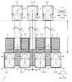
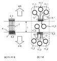
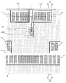
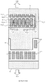
도 1은 실시 형태 1 또는 실시 형태 2에 따른 반도체 칩에 있어서의 패드의 배치를 도시하는 레이아웃도이다.
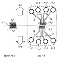
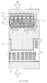
도 2는 종래의 반도체 칩에 있어서의 패드의 배치를 도시하는 레이아웃도.
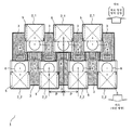
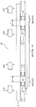
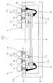
도 3은 실시 형태 1 또는 실시 형태 2에 따른 반도체 칩이 기판 상에 플립 칩 실장된, 반도체 장치의 단면 방향의 실장 상태를 도시하는 모식도.
도 4는 실시 형태 1 또는 실시 형태 2에 따른 반도체 칩에 있어서의 패드의 레이아웃과, 그것이 플립 칩 실장되는 기판에 있어서의 기판 패드의 레이아웃을 도시하는 모식도.
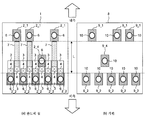
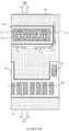
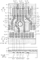
도 5는 실시 형태 1에 따른 반도체 칩이 플립 칩 실장되는 기판에 있어서의, 기판 패드의 배치를 도시하는 레이아웃도.
도 6은 종래의 반도체 칩에 있어서의 패드의 배치예와, 그 반도체 칩이 플립 칩 실장되는 기판에 있어서의, 기판 패드의 배치예를 도시하는 레이아웃도.
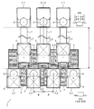
도 7은, 실시 형태 1에 따른 반도체 칩에 있어서의 패드의 배치예와 그 반도체 칩이 플립 칩 실장되는 기판에 있어서의, 기판 패드의 배치예를 도시하는 레이아웃도.
도 8은 실시 형태 1에 따른 반도체 칩에 있어서의 패드의 배치예와 그 반도체 칩이 플립 칩 실장되는 기판에 있어서의, 기판 패드의 배치의 다른 예를 도시하는 레이아웃도.
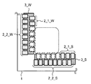
도 9는 실시 형태 2에 따른 반도체 칩이 플립 칩 실장되는 기판에 있어서의, 기판 패드의 배치를 도시하는 레이아웃도.
도 10은 실시 형태 3에 따른 반도체 칩에 있어서의 패드의 배치를 도시하는 레이아웃도.
도 11은 종래의 반도체 칩의 코너부에 있어서의 패드의 배치를 도시하는 레이아웃도.
도 12는 실시 형태 4에 따른 반도체 칩의 코너부에 있어서의 패드의 배치를 도시하는 레이아웃도.
도 13은 실시 형태 1 내지 4에 따른 반도체 칩이 플립 칩 실장된 기판을 포함하는, BGA의 단면 방향의 실장 형태의 일례를 도시하는 모식도.
도 14는 실시 형태 1 내지 4에 따른 반도체 칩이 플립 칩 실장된 기판을 포함하는, SiP(System in Package)의 단면 방향의 실장 형태의 일례를 도시하는 모식도.
도 15는 실시 형태 1 내지 4에 따른 반도체 칩이 플립 칩 실장된 기판을 포함하는, PoP(Package on Package)의 단면 방향의 실장 형태의 일례를 도시하는 모식도.
도 16은 실시 형태 1 내지 4에 따른 반도체 칩이 기판 상에 베어 칩인 상태로 플립 칩 실장된 회로 기판에 있어서의, 단면 방향의 실장 형태의 일례를 도시하는 모식도.
도 17은 새로운 과제에 관한 설명도.
도 18은 새로운 과제에 관한 보다 상세한 설명도.
도 19는 실시 형태 6에 따른 반도체 칩이 기판 상에 플립 칩 실장된, 반도체 장치의 평면 방향 및 단면 방향의 실장 상태를 도시하는 모식도.
도 20은 실시 형태 6에 따른 반도체 장치의 기판에 있어서의, 기판 패드의 배치의 일례를 도시하는 레이아웃도.
도 21은 실시 형태 6에 따른 반도체 장치의 기판에 있어서의, 기판 패드의 배치의 다른 예를 도시하는 레이아웃도.
도 22는 실시 형태 6에 따른 반도체 장치의 기판에 있어서의, 기판 패드의 배치의 또 다른 예를 도시하는 레이아웃도.
도 23은 실시 형태 7에 따른 반도체 장치의 기판에 있어서의, 솔더 레지스트 개구부의 형상의 일례를 도시하는 레이아웃도.
도 24는 실시 형태 8에 따른 반도체 장치의 기판에 있어서의, 기판 패드의 배치의 일례를 도시하는 레이아웃도.
도 25는 실시 형태 9에 따른 반도체 장치의 기판에 있어서의, 솔더 레지스트 개구부 내에 배치되는 기판 패드의 형상의 일례를 도시하는 레이아웃도.
도 26은 실시 형태 10에 따른 반도체 장치의 기판에 있어서의, 기판 패드 및 배선의 배치의 일례를 도시하는 레이아웃도.1 is a layout diagram showing the arrangement of pads in the semiconductor chip according to the first or second embodiment.
2 is a layout diagram showing the arrangement of pads in a conventional semiconductor chip.
3 is a schematic diagram showing a mounting state of a semiconductor device in a cross-sectional direction in which a semiconductor chip according to
4 is a schematic diagram showing the layout of the pads in the semiconductor chip according to the first or second embodiment and the layout of the substrate pads in the substrate on which the flip chip is mounted.
5 is a layout view showing the arrangement of substrate pads in a substrate on which a semiconductor chip according to
6 is a layout diagram showing an example of arrangement of pads in a conventional semiconductor chip and an example of arrangement of substrate pads in a substrate on which the semiconductor chip is flip-chip mounted.
Fig. 7 is a layout diagram showing an example of arrangement of pads in the semiconductor chip according to the first embodiment and an example of arrangement of the substrate pads in a substrate on which the semiconductor chips are flip-chip mounted. Fig.
8 is a layout diagram showing another example of the arrangement of pads in the semiconductor chip according to the first embodiment and the arrangement of the substrate pads in the substrate on which the semiconductor chips are mounted by flip-chip mounting.
9 is a layout view showing the arrangement of substrate pads in the substrate on which the semiconductor chip according to the second embodiment is mounted by flip-chip mounting.
10 is a layout view showing the arrangement of pads in the semiconductor chip according to the third embodiment;
11 is a layout view showing the arrangement of pads in a corner portion of a conventional semiconductor chip.
12 is a layout view showing the arrangement of pads in the corner portion of the semiconductor chip according to the fourth embodiment;
13 is a schematic diagram showing an example of a mounting form of the BGA in the cross-sectional direction, including the substrate on which the semiconductor chip according to the first to fourth embodiments is flip-chip mounted.
14 is a schematic diagram showing an example of a mounting form of the SiP (System in Package) in the cross-sectional direction, including the substrate on which the semiconductor chip according to the first to fourth embodiments is flip-chip mounted.
15 is a schematic diagram showing an example of a mounting form of a package on package (PoP) in a cross-sectional direction, including a substrate on which a semiconductor chip according to any of the first to fourth embodiments is flip-chip mounted.
16 is a schematic diagram showing an example of a mounting form in a cross-sectional direction in a circuit board on which a semiconductor chip according to any of the first to fourth embodiments is flip-chip mounted with a bare chip on a board.
17 is an explanatory diagram relating to a new problem.
Figure 18 is a more detailed illustration of a new task.
19 is a schematic diagram showing a mounting state in a plane direction and a cross-sectional direction of a semiconductor device in which a semiconductor chip according to a sixth embodiment is flip-chip mounted on a substrate.
20 is a layout view showing an example of the arrangement of substrate pads in the substrate of the semiconductor device according to the sixth embodiment;
21 is a layout view showing another example of the arrangement of substrate pads in the substrate of the semiconductor device according to the sixth embodiment;
22 is a layout view showing another example of the arrangement of substrate pads in the substrate of the semiconductor device according to the sixth embodiment;
23 is a layout view showing an example of the shape of a solder resist opening portion in the substrate of the semiconductor device according to the seventh embodiment;
24 is a layout view showing an example of the arrangement of substrate pads in the substrate of the semiconductor device according to the eighth embodiment;
Fig. 25 is a layout view showing an example of the shape of a substrate pad disposed in a solder resist opening portion in a substrate of a semiconductor device according to
26 is a layout view showing an example of the arrangement of substrate pads and wirings in the substrate of the semiconductor device according to the tenth embodiment;
1. 실시 형태의 개요1. Overview of Embodiment
우선, 본원에 있어서 개시되는 대표적인 실시 형태에 대하여 개요를 설명한다. 대표적인 실시 형태에 따른 개요 설명에서 괄호를 붙여서 참조하는 도면 중의 참조 부호는 그것이 붙여진 구성 요소의 개념에 포함되는 것을 예시한 것에 불과하다.First, the outline of a representative embodiment disclosed in the present application will be described. Reference numerals in the drawings referred to by parentheses in the outline explanation according to the exemplary embodiment are merely illustrative of those included in the concept of the attached components.
〔1〕<실장 완료 LSI; 내측과 외측의 패드의 간격을 확대>[1] < Implemented LSI; Expansion of spacing between inner and outer pads>
복수의 칩 패드(2)를 구비하는 반도체 칩(1)과, 상기 반도체 칩이 플립 칩 실장되고, 상기 칩 패드와 접속되는 기판 패드(9)과 비아(11)를 구비한 기판(8)을 구비하는 반도체 장치(20)로서, 이하와 같이 구성된다.A semiconductor device comprising: a semiconductor chip (1) having a plurality of chip pads (2); a substrate pad (9) having the semiconductor chip flip chip mounted thereon and connected to the chip pads; The
상기 반도체 칩은, 직선 형상으로 배열되고, 인접하는 제1 입출력 셀(3_1)과 제2 입출력 셀(3_2)과 제3 입출력 셀(3_3)을 포함하는, 복수의 입출력 셀(3)을 포함하는 입출력 셀열을 구비한다. 상기 복수의 칩 패드는, 상기 제1 입출력 셀에 전기적으로 접속되는 제1 패드(2_2_1)와 상기 제2 입출력 셀에 전기적으로 접속되는 제2 패드(2_1_2)와 상기 제3 입출력 셀에 전기적으로 접속되는 제3 패드(2_2_3)를 포함한다.The semiconductor chip includes a plurality of input / output cells (3) arranged in a straight line and including adjacent first input / output cells (3_1), second input / output cells (3_2) and third input / output cells (3_3) And an input / output cell array. The plurality of chip pads includes a first pad (2_2_1) electrically connected to the first input / output cell, a second pad (2_1_2) electrically connected to the second input / output cell, and a second pad electrically connected to the third input / And a third pad 2_2_3.
상기 기판은, 상기 제1 패드와 대면하여 접속되는 제1 기판 패드(9_2_1)와, 상기 제2 패드와 대면하여 접속되는 제2 기판 패드(9_1_2)와, 상기 제3 패드와 대면하여 접속되는 제3 기판 패드(9_2_3)를 구비한다. 상기 제1 기판 패드와 상기 제3 기판 패드의 간격은, 상기 기판의 설계 제약에서 허용되는 배선의 최소폭과, 배선과 기판 패드에 요구되는 스페이스값의 2배의 합보다도 좁다.The substrate includes a first substrate pad (9_2_1) connected to the first pad in a face-to-face relationship, a second substrate pad (9_1_2) connected to face the second pad, and a
상기 반도체 칩에 있어서, 상기 제1 패드와 상기 제3 패드는 상기 입출력 셀열보다 외측에 서로 인접하여 배열된다. 상기 제2 패드는, 상기 입출력 셀열보다 내측에 배치되고, 상기 제1 패드와 상기 제3 패드 각각으로부터 소정의 거리를 이격하여 배치된다. 상기 소정의 거리란, 상기 반도체 칩이 플립 칩 실장되는 기판에 설치되는 비아의 직경(L1)과, 상기 비아와 상기 기판 패드의 간격에 설계 제약에서 요구되는 최소 스페이스값(L2)의 2배의 합 이상의 거리(L)이다.In the semiconductor chip, the first pad and the third pad are arranged adjacently to each other outside the input / output cell array. The second pad is disposed on the inner side of the input / output cell array and is spaced apart from the first pad and the third pad by a predetermined distance. The predetermined distance is defined as a distance L1 between a diameter of the via formed in the substrate on which the semiconductor chip is mounted and a distance between the via and the substrate pad that is twice the minimum space value L2 (L).
이에 의해, 반도체 칩이 플립 칩 실장되는 기판의 배선성을 향상시킬 수 있다. 특히, 기판 상의 신호 배선이나 전원 배선의 배선성을 향상시킬 수 있다.Thereby, the wiring property of the substrate on which the semiconductor chip is flip-chip mounted can be improved. In particular, it is possible to improve the wiring property of the signal wiring and the power wiring on the substrate.
〔2〕<외측의 패드(out-line pad)는, 최소 피치로 직선 형상으로 배열>[2] < Out-line pads are arranged in a linear shape with a minimum pitch >
항1에 있어서, 상기 반도체 칩은, 상기 제1 패드와 상기 제3 패드를 포함하는 복수의 패드가 서로 인접하여, 상기 입출력 셀열과 평행하고 상기 입출력 셀열보다 외측에 직선 형상으로 배열되는, 제1 패드열(2_2)을 구비하고, 상기 제1 패드열에 있어서 서로 인접하여 배열되는 복수의 패드는, 상기 반도체 칩의 패드끼리의 간격에 설계 제약에서 요구되는 최소의 피치로 배치된다.2. The semiconductor device according to
이에 의해, 반도체 칩(1)의 칩 크기가 단자수에 의해 결정되는 패드 넥인 경우에도, 종래와 동일한 칩 크기로 억제할 수 있다.Thus, even when the chip size of the
〔3〕<내측의 패드(in-line pad)도 최소 피치로 직선 형상으로 배열>[3] <In-line pads are also arranged in a linear shape with a minimum pitch>
항2에 있어서, 상기 반도체 칩은, 상기 제2 패드를 포함하는 복수의 패드가 서로 인접하여, 상기 입출력 셀열과 평행하고 상기 입출력 셀열보다 내측에 직선 형상으로 배열되는, 제2 패드열(2_1)을 구비하고, 상기 제2 패드열에 있어서 서로 인접하여 배열되는 복수의 패드는, 상기 반도체 칩의 패드끼리의 간격에 설계 제약에서 요구되는 최소의 피치로 배치된다.The semiconductor chip according to
이에 의해, 반도체 칩(1)에 있어서, 종래와 동일수의 패드수(단자수)를 확보할 수 있다.As a result, it is possible to secure the same number of pads (the number of terminals) as in the
〔4〕<프로브용 패드>[4] <Pads for probes>
항1에 있어서, 상기 반도체 칩은, 상기 제2 입출력 셀에 전기적으로 접속되고, 상기 입출력 셀열보다 내측이고 상기 제2 패드와 상기 입출력 셀열 사이에 배치되는, 제4 패드(2_3)를 더 구비한다.The semiconductor device of
이에 의해, 프로브용 패드를, 프로빙을 위한 바늘 접촉 압력이 내부 회로에 가해지지 않는 위치에 배치할 수 있다.Thereby, the probe pads can be arranged at positions where the needle contact pressure for probing is not applied to the internal circuit.
상기 기판은, 상기 제1 패드와 대면하여 접속되는 제1 기판 패드(9_2_1)와, 상기 제2 패드와 대면하여 접속되는 제2 기판 패드(9_1_2)와, 상기 제3 패드와 대면하여 접속되는 제3 기판 패드(9_2_3)를 구비하고, 상기 제4 패드와 대면하는 위치에 기판 패드를 배치하지 않는다.The substrate includes a first substrate pad (9_2_1) connected to the first pad in a face-to-face relationship, a second substrate pad (9_1_2) connected to face the second pad, and a
〔5〕<코너부>[5] <corner part>
항3에 있어서, 상기 반도체 칩은, 상기 입출력 셀열을 제1 입출력 셀열(3_W)로 하고, 상기 반도체 칩의 1개의 코너부에서 상기 제1 입출력 셀열과 직각 방향으로 직선 형상으로 배열된 복수의 입출력 셀을 제2 입출력 셀열(3_S)로 하고, 상기 제2 입출력 셀열과 평행하고 상기 제2 입출력 셀열보다 외측에 직선 형상으로 배열되는, 제3 패드열(2_2_S)을 구비한다. 상기 제3 패드열에 있어서 서로 인접하여 배열되는 복수의 패드는, 상기 반도체 칩의 패드끼리의 간격에 설계 제약에서 요구되는 최소의 피치로 배치된다.The semiconductor chip according to
이에 의해, 반도체 칩(1)의 코너부에 있어서, 배치하는 패드의 수를 종래보다도 증가시킬 수 있다.As a result, the number of pads to be arranged at the corner of the
〔6〕<근접하는 입출력 셀에 접속되는 패드간에서 비아를 공유>[6] <Vias are shared between pads connected to adjacent input / output cells>
항1에 있어서, 상기 기판은, 상기 제1 패드와 대면하여 접속되는 제1 기판 패드(9_2_1)와, 상기 제2 패드와 대면하여 접속되는 제2 기판 패드(9_1_2)와, 상기 제3 패드와 대면하여 접속되는 제3 기판 패드(9_2_3)를 구비한다. 상기 기판은, 상기 제1 기판 패드와 상기 제2 기판 패드와 동일한 배선층에서 상기 제1 기판 패드와 상기 제2 기판 패드를 접속하는 배선과, 상기 배선에 접속되고 상기 제1 기판 패드와 상기 제2 기판 패드 사이에 배치되는 비아(11_4)를 구비한다.The semiconductor device of
이에 의해, 내측 패드열과 외측 패드열에서, 서로 근접하는 입출력 셀에 접속되는 칩 패드가, 동일한 신호인 경우, 대응하는 기판 패드를 서로 단락하여 비아를 공유함으로써, 기판의 배선성을 더 향상시킬 수 있다. 특히, 근접하는 패드가 모두 전원이나 그라운드인 경우에 유효하다.Thus, when the chip pads connected to the input / output cells adjacent to each other in the inner pad row and the outer pad row are the same signal, the corresponding substrate pads are short-circuited to share vias, thereby further improving the wiring property of the substrate have. Especially, it is effective when all adjacent pads are power or ground.
〔7〕<BGA>[7] <BGA>
항1 내지 항6 중 어느 한 항에 있어서, 상기 기판은, 상기 기판 패드를 구비하는 면과 반대 면에, BGA 패드(22)를 구비하고, 상기 BGA 패드에 접속되는 BGA 전극(23)을 구비한다.6. The semiconductor device according to any one of
이에 의해, BGA에 실장된 반도체 장치(20_1)에 있어서, 기판의 배선성을 향상시킬 수 있다.Thus, in the semiconductor device 20_1 mounted on the BGA, the wiring property of the substrate can be improved.
〔8〕<SiP(System in Package)>[8] SiP (System in Package)
항7에 있어서, 상기 반도체 칩을 제1 반도체 칩(1)으로 하고, 상기 제1 반도체 칩에 적층된, 제2 반도체 칩(24)을 더 구비한다. 상기 기판 패드를 제1 기판 패드군(9_1, 9_2)으로 하고, 상기 기판은, 상기 제1 기판 패드군과 동일한 면에 상기 제1 기판 패드군과는 상이한 제2 기판 패드군(9_4)을 더 구비하고, 상기 제2 반도체 칩은 상기 제2 기판 패드군과 본딩와이어(25)에 의해 접속된다.The semiconductor device according to
이에 의해, SiP(20_2)에 있어서, 기판의 배선성을 향상시킬 수 있다.Thereby, the wiring property of the substrate can be improved in the SiP 20_2.
〔9〕<PoP(Package on Package)>[9] < PoP (Package on Package) >
항7에 있어서, 돌기 전극(27)을 구비하는 패키지 실장된 제2 반도체 장치(26)를 더 구비한다.The semiconductor device according to
상기 기판 패드를 제1 기판 패드군(9_1, 9_2)으로 하고, 상기 기판은, 상기 제1 기판 패드군과 동일한 면에 상기 제1 기판 패드군과는 상이한 제2 기판 패드군(9_4)을 더 구비하고, 상기 돌기 전극과 상기 제2 기판 패드군을 접속함으로써, 상기 제2 반도체 장치가 적층된다.The substrate pads are made of first substrate pad groups 9_1 and 9_2 and the substrate has a second substrate pad group 9_4 different from the first substrate pad group on the same surface as the first substrate pad group And the second semiconductor device is stacked by connecting the protruding electrode and the second substrate pad group.
이에 의해, PoP(20_3)에 있어서, 기판의 배선성을 향상시킬 수 있다.As a result, the wiring property of the substrate can be improved in the PoP 20_3.
〔10〕<플립 칩용 반도체 칩; 내측과 외측의 패드의 간격을 확대>[10] < Flip Chip Semiconductor Chip; Expansion of spacing between inner and outer pads>
반도체 칩(1)은 직선 형상으로 배열되고, 인접하는 제1 입출력 셀(3_1)과 제2 입출력 셀(3_2)과 제3 입출력 셀(3_3)을 포함하는, 복수의 입출력 셀(3)을 포함하는 입출력 셀열을 구비한다. 또한, 반도체 칩(1)은, 상기 제1 입출력 셀에 전기적으로 접속되는 제1 패드(2_2_1)와 상기 제2 입출력 셀에 전기적으로 접속되는 제2 패드(2_1_2)와 상기 제3 입출력 셀에 전기적으로 접속되는 제3 패드(2_2_3)를 구비한다.The
상기 반도체 칩이 플립 칩 실장되는 기판(8)은, 상기 제1 패드와 대면하여 접속되는 제1 기판 패드(9_2_1)와, 상기 제2 패드와 대면하여 접속되는 제2 기판 패드(9_1_2)와, 상기 제3 패드와 대면하여 접속되는 제3 기판 패드(9_2_3)를 구비한다. 상기 제1 기판 패드와 상기 제3 기판 패드의 간격은, 상기 기판의 설계 제약에서 허용되는 배선의 최소폭과, 배선과 기판 패드에 요구되는 스페이스값의 2배의 합보다도 좁다.The
상기 제1 패드와 상기 제3 패드는 상기 입출력 셀열보다 외측에 서로 인접하여 배열되고, 상기 제2 패드는, 상기 입출력 셀열보다 내측에 배치된다. 상기 제2 패드는, 상기 반도체 칩이 플립 칩 실장되는 기판에 설치되는 비아의 직경(L1)과, 상기 비아와 상기 반도체 칩의 패드와 접속되는 상기 기판 상의 기판 패드의 간격에 설계 제약에서 요구되는 최소 스페이스값(L2)의 2배의 합 이상의 거리(L)를 상기 제1 패드와 상기 제3 패드 각각으로부터 이격하여 배치된다.The first pad and the third pad are arranged adjacent to each other on the outer side of the input / output cell array, and the second pad is disposed on the inner side of the input / output cell array. Wherein the second pad has a diameter (L1) of a via provided on a substrate on which the semiconductor chip is to be flip-chip mounted and a gap between the via and the pad of the semiconductor chip And a distance L equal to or greater than twice the minimum space value L2 is disposed apart from the first pad and the third pad.
이에 의해, 반도체 칩이 플립 칩 실장되는 기판의 배선성을 향상시킬 수 있다. 특히, 기판 상의 신호 배선이나 전원 배선의 배선성을 향상시킬 수 있다.Thereby, the wiring property of the substrate on which the semiconductor chip is flip-chip mounted can be improved. In particular, it is possible to improve the wiring property of the signal wiring and the power wiring on the substrate.
〔11〕<외측의 패드(out-line pad)는 최소 피치로 직선 형상으로 배열>[11] Out-line pads are arranged in a linear shape with a minimum pitch.
항10에 있어서, 상기 제1 패드와 상기 제3 패드를 포함하는 복수의 패드가 서로 인접하여, 상기 입출력 셀열과 평행하고 상기 입출력 셀열보다 외측에 직선 형상으로 배열되는, 제1 패드열(2_2)을 구비하고, 상기 제1 패드열에 있어서 서로 인접하여 배열되는 복수의 패드는, 상기 반도체 칩의 패드끼리의 간격에 설계 제약에서 요구되는 최소의 피치로 배치된다.10. The semiconductor device according to
이에 의해, 반도체 칩(1)의 칩 크기가 단자수에 의해 결정되는 패드 넥인 경우에도, 종래와 동일한 칩 크기로 억제할 수 있다.Thus, even when the chip size of the
〔12〕<내측의 패드(in-line pad)도 최소 피치로 직선 형상으로 배열>[12] <In-line pads are also arranged in a linear shape with a minimum pitch>
항11에 있어서, 상기 제2 패드를 포함하는 복수의 패드가 서로 인접하여, 상기 입출력 셀열과 평행하고 상기 입출력 셀열보다 내측에 직선 형상으로 배열되는, 제2 패드열(2_1)을 구비하고, 상기 제2 패드열에 있어서 서로 인접하여 배열되는 복수의 패드는, 상기 반도체 칩의 패드끼리의 간격에 설계 제약에서 요구되는 최소의 피치로 배치된다.The apparatus of
이에 의해, 반도체 칩(1)에 있어서, 종래와 동일수의 패드수(단자수)를 확보할 수 있다.As a result, it is possible to secure the same number of pads (the number of terminals) as in the
〔13〕<프로브용 패드>[13] <Pad for probe>
항10에 있어서, 상기 반도체 칩은, 상기 제2 입출력 셀에 전기적으로 접속되고, 상기 입출력 셀열보다 내측이고 상기 제2 패드와 상기 입출력 셀열 사이에 배치되는, 제4 패드(2_3)를 더 구비한다.The semiconductor chip of
이에 의해, 프로브용 패드를, 프로빙을 위한 바늘 접촉 압력이 내부 회로에 가해지지 않는 위치에 배치할 수 있다.Thereby, the probe pads can be arranged at positions where the needle contact pressure for probing is not applied to the internal circuit.
〔14〕<코너부>[14] <corner part>
항12에 있어서, 상기 입출력 셀열을 제1 입출력 셀열(3_W)로 하고, 상기 반도체 칩의 1개의 코너부에서 상기 제1 입출력 셀열과 직각 방향으로 직선 형상으로 배열된 복수의 입출력 셀을 제2 입출력 셀열(3_S)로 하고, 상기 제2 입출력 셀열과 평행하고 상기 제2 입출력 셀열보다 외측에 직선 형상으로 배열되는, 제3 패드열(2_2_S)을 구비한다.Output cell column as a first input / output cell array (3_W), and a plurality of input / output cells arranged linearly at one corner of the semiconductor chip in a direction perpendicular to the first input / output cell column are connected to a second input / And a third pad column 2_2_S arranged as a cell column 3_S and arranged in a straight line outside the second input / output cell column and parallel to the second input / output cell column.
상기 제3 패드열에 있어서 서로 인접하여 배열되는 복수의 패드는, 상기 반도체 칩의 패드끼리의 간격에 설계 제약에서 요구되는 최소의 피치로 배치된다.The plurality of pads arranged adjacent to each other in the third pad column are arranged at the minimum pitch required for the design constraint in the interval between the pads of the semiconductor chip.
이에 의해, 반도체 칩(1)의 코너부에 있어서, 배치하는 패드의 수를 종래보다도 증가시킬 수 있다.As a result, the number of pads to be arranged at the corner of the
〔15〕<실장 완료; LSI 내측과 외측의 패드의 간격을 도금 배선분 확대>[15] < Implementation completion; The distance between the pad inside and outside of the LSI is enlarged by plating wiring.
복수의 칩 패드(2)를 구비하는 반도체 칩(1)과, 상기 반도체 칩이 플립 칩 실장되는 기판(8)을 구비하는 반도체 장치(20)로서, 이하와 같이 구성된다.A semiconductor device (20) including a semiconductor chip (1) having a plurality of chip pads (2) and a substrate (8) on which the semiconductor chip is mounted by flip chip mounting.
상기 기판은, 상기 칩 패드와 접속되는 기판 패드(9)와, 상기 기판 패드와 동일한 배선층의 배선(12_1 내지 12_6)과, 상기 배선의 적어도 일부를 피복하는 레지스트막(13)을 구비한다.The substrate includes a substrate pad (9) connected to the chip pad, wirings (12_1 to 12_6) in the same wiring layer as the substrate pad, and a resist film (13) covering at least a part of the wiring.
상기 반도체 칩은, 직선 형상으로 배열되고, 인접하는 제1 입출력 셀(3_1)과 제2 입출력 셀(3_2)과 제3 입출력 셀(3_3)을 포함하는, 복수의 입출력 셀(3)을 포함하는 입출력 셀열을 구비한다. 상기 복수의 칩 패드는, 상기 제1 입출력 셀에 전기적으로 접속되는 제1 패드(2_2_1)와 상기 제2 입출력 셀에 전기적으로 접속되는 제2 패드(2_1_2)와 상기 제3 입출력 셀에 전기적으로 접속되는 제3 패드(2_2_3)를 포함한다.The semiconductor chip includes a plurality of input / output cells (3) arranged in a straight line and including adjacent first input / output cells (3_1), second input / output cells (3_2) and third input / output cells (3_3) And an input / output cell array. The plurality of chip pads includes a first pad (2_2_1) electrically connected to the first input / output cell, a second pad (2_1_2) electrically connected to the second input / output cell, and a second pad electrically connected to the third input / And a third pad 2_2_3.
상기 기판은, 상기 제1 패드와 대면하여 접속되는 제1 기판 패드(9_2_1)와, 상기 제2 패드와 대면하여 접속되는 제2 기판 패드(9_1_2)와, 상기 제3 패드와 대면하여 접속되는 제3 기판 패드(9_2_3)를 구비한다. 상기 제1 기판 패드와 상기 제3 기판 패드의 간격은, 상기 기판의 설계 제약에서 허용되는 배선의 최소폭과, 배선과 기판 패드에 요구되는 스페이스값의 2배의 합보다도 좁다.The substrate includes a first substrate pad (9_2_1) connected to the first pad in a face-to-face relationship, a second substrate pad (9_1_2) connected to face the second pad, and a
상기 반도체 칩에 있어서, 상기 제1 패드와 상기 제3 패드는 상기 입출력 셀열보다 외측에 서로 인접하여 배열되고, 상기 제2 패드는, 상기 입출력 셀열보다 내측에 배치된다.In the semiconductor chip, the first pad and the third pad are arranged adjacently to each other outside the input / output cell array, and the second pad is disposed inside the input / output cell array.
상기 기판에 있어서, 상기 제2 기판 패드와 상기 제1 및 상기 제3 기판 패드 사이의 레지스트막(13_2, 13_3)에, 상기 제1, 제2 및 제3 기판 패드를 단락하는 도금 배선(12_1)을 에치 백하기 위한 개구부를 형성한다.The plating wiring 12_1 for short-circuiting the first, second, and third substrate pads is formed on the resist film 13_2, 13_3 between the second substrate pad and the first and third substrate pads, An opening for etching back is formed.
이에 의해, 반도체 칩이 플립 칩 실장되는 기판의 배선성을 향상시킬 수 있다. 특히, 기판 상의 도금 배선의 배선성을 향상시킬 수 있다.Thereby, the wiring property of the substrate on which the semiconductor chip is flip-chip mounted can be improved. In particular, the wiring property of the plating wiring on the substrate can be improved.
〔16〕<외측의 패드(out-line pad)는, 최소 피치로 직선 형상으로 배열>(16) Out-line pads are arranged in a linear shape with a minimum pitch.
항15에 있어서, 상기 반도체 칩은, 상기 제1 패드와 상기 제3 패드를 포함하는 복수의 패드가 서로 인접하여, 상기 입출력 셀열과 평행하고 상기 입출력 셀열보다 외측에 직선 형상으로 배열되는, 제1 패드열(2_2)을 구비하고, 상기 제1 패드열에 있어서 서로 인접하여 배열되는 복수의 패드는, 상기 반도체 칩의 패드끼리의 간격에 설계 제약에서 요구되는 최소의 피치로 배치된다.15. The semiconductor chip according to
이에 의해, 반도체 칩(1)의 칩 크기가 단자수에 의해 결정되는 패드 넥인 경우에도, 종래와 동일한 칩 크기로 억제할 수 있다.Thus, even when the chip size of the
〔17〕<내측의 패드(in-line pad)도 최소 피치로 직선 형상으로 배열>[17] <In-line pads are also arranged in a linear shape with a minimum pitch>
항16에 있어서, 상기 반도체 칩은, 상기 제2 패드를 포함하는 복수의 패드가 서로 인접하여, 상기 입출력 셀열과 평행하고 상기 입출력 셀열보다 내측에 직선 형상으로 배열되는, 제2 패드열(2_1)을 구비하고, 상기 제2 패드열에 있어서 서로 인접하여 배열되는 복수의 패드는, 상기 반도체 칩의 패드끼리의 간격에 설계 제약에서 요구되는 최소의 피치로 배치된다.The semiconductor chip according to
이에 의해, 반도체 칩(1)에 있어서, 종래와 동일수의 패드수(단자수)를 확보할 수 있다.As a result, it is possible to secure the same number of pads (the number of terminals) as in the
〔18〕<프로브용 패드>[18] <Pads for probes>
항15에 있어서, 상기 반도체 칩은, 상기 제2 입출력 셀에 전기적으로 접속되고, 상기 입출력 셀열보다 내측이고 상기 제2 패드와 상기 입출력 셀열 사이에 배치되는, 제4 패드(2_3)를 더 구비한다.The semiconductor chip according to
이에 의해, 프로브용 패드를, 프로빙을 위한 바늘 접촉 압력이 내부 회로에 가해지지 않는 위치에 배치할 수 있다.Thereby, the probe pads can be arranged at positions where the needle contact pressure for probing is not applied to the internal circuit.
상기 기판은, 상기 제1 패드와 대면하여 접속되는 제1 기판 패드(9_2_1)와, 상기 제2 패드와 대면하여 접속되는 제2 기판 패드(9_1_2)와, 상기 제3 패드와 대면하여 접속되는 제3 기판 패드(9_2_3)를 구비하고, 상기 제4 패드와 대면하는 위치에 기판 패드를 배치하지 않는다.The substrate includes a first substrate pad (9_2_1) connected to the first pad in a face-to-face relationship, a second substrate pad (9_1_2) connected to face the second pad, and a
〔19〕<코너부>[19] <corner part>
항17에 있어서, 상기 반도체 칩은, 상기 입출력 셀열을 제1 입출력 셀열(3_W)로 하고, 상기 반도체 칩의 1개의 코너부에서 상기 제1 입출력 셀열과 직각 방향으로 직선 형상으로 배열된 복수의 입출력 셀을 제2 입출력 셀열(3_S)로 하고, 상기 제2 입출력 셀열과 평행하고 상기 제2 입출력 셀열보다 외측에 직선 형상으로 배열되는, 제3 패드열(2_2_S)을 구비한다. 상기 제3 패드열에 있어서 서로 인접하여 배열되는 복수의 패드는, 상기 반도체 칩의 패드끼리의 간격에 설계 제약에서 요구되는 최소의 피치로 배치된다.The semiconductor chip according to
이에 의해, 반도체 칩(1)의 코너부에, 배치 가능한 패드수를 종래보다도 증가시킬 수 있다.Thereby, the number of pads that can be arranged at the corner of the
〔20〕<근접하는 입출력 셀에 접속되는 패드간에서 비아를 공유>[20] <Vias are shared between pads connected to adjacent input / output cells>
항15에 있어서, 상기 기판은, 상기 제1 기판 패드와 상기 제2 기판 패드와 동일한 배선층에서 상기 제1 기판 패드와 상기 제2 기판 패드를 접속하는 배선과, 상기 배선에 접속되고 상기 제1 기판 패드와 상기 제2 기판 패드 사이에 배치되는 비아(11_4)를 구비한다.15. The substrate of
이에 의해, 내측 패드열과 외측 패드열에서, 서로 근접하는 입출력 셀에 접속되는 칩 패드가, 동일한 신호인 경우, 대응하는 기판 패드를 서로 단락하여 비아를 공유함으로써 기판의 배선성을 보다 향상시킬 수 있다. 특히, 근접하는 패드가 모두 전원이나 그라운드인 경우에 유효하다.Thus, when the chip pads connected to the input / output cells adjacent to each other in the inner pad column and the outer pad column are the same signal, the corresponding board pads are short-circuited to each other to share vias, thereby further improving the wiring property of the substrate . Especially, it is effective when all adjacent pads are power or ground.
〔21〕<BGA>[21] <BGA>
항15 내지 항20 중 어느 한 항에 있어서, 상기 기판은, 상기 기판 패드를 구비하는 면과 반대 면에, BGA 패드(22)를 구비하고, 상기 BGA 패드에 접속되는 BGA 전극(23)을 구비한다.
이에 의해, BGA에 실장된 반도체 장치(20_1)에 있어서, 기판의 배선성을 향상시킬 수 있다.Thus, in the semiconductor device 20_1 mounted on the BGA, the wiring property of the substrate can be improved.
〔22〕<SiP>[22] < SiP >
항(21)에 있어서, 상기 반도체 칩을 제1 반도체 칩(1)으로 하고, 상기 제1 반도체 칩에 적층된, 제2 반도체 칩(24)을 더 구비한다. 상기 기판 패드를 제1 기판 패드군(9_1, 9_2)으로 하고, 상기 기판은, 상기 제1 기판 패드군과 동일한 면에 상기 제1 기판 패드군과는 상이한 제2 기판 패드군(9_4)을 더 구비하고, 상기 제2 반도체 칩은 상기 제2 기판 패드군과 본딩와이어(25)에 의해 접속된다.Item (21) further includes a second semiconductor chip (24) stacked on the first semiconductor chip, wherein the semiconductor chip is a first semiconductor chip (1). The substrate pads are made of first substrate pad groups 9_1 and 9_2 and the substrate has a second substrate pad group 9_4 different from the first substrate pad group on the same surface as the first substrate pad group And the second semiconductor chip is connected to the second substrate pad group by a bonding wire (25).
이에 의해, SiP(20_2)에 있어서, 기판의 배선성을 향상시킬 수 있다.Thereby, the wiring property of the substrate can be improved in the SiP 20_2.
〔23〕<PoP>[23] <PoP>
항(21)에 있어서, 돌기 전극(27)을 구비하는 패키지 실장된 제2 반도체 장치(26)를 더 구비한다.
상기 기판 패드를 제1 기판 패드군(9_1, 9_2)으로 하고, 상기 기판은, 상기 제1 기판 패드군과 동일한 면에 상기 제1 기판 패드군과는 상이한 제2 기판 패드군(9_4)을 더 구비하고, 상기 돌기 전극과 상기 제2 기판 패드군을 접속함으로써, 상기 제2 반도체 장치가 적층된다.The substrate pads are made of first substrate pad groups 9_1 and 9_2 and the substrate has a second substrate pad group 9_4 different from the first substrate pad group on the same surface as the first substrate pad group And the second semiconductor device is stacked by connecting the protruding electrode and the second substrate pad group.
이에 의해, PoP(20_3)에 있어서, 기판의 배선성을 향상시킬 수 있다.As a result, the wiring property of the substrate can be improved in the PoP 20_3.
〔24〕<플립 칩용 반도체 칩; 내측과 외측의 패드의 간격을 도금 배선분 확대>[24] < Flip Chip Semiconductor Chip; The gap between the inner and outer pads is enlarged by plating wiring.
반도체 칩(1)은 직선 형상으로 배열되고, 인접하는 제1 입출력 셀(3_1)과 제2 입출력 셀(3_2)과 제3 입출력 셀(3_3)을 포함하는, 복수의 입출력 셀(3)을 포함하는 입출력 셀열을 구비한다. 또한, 반도체 칩(1)은 상기 제1 입출력 셀에 전기적으로 접속되는 제1 패드(2_2_1)와 상기 제2 입출력 셀에 전기적으로 접속되는 제2 패드(2_1_2)와 상기 제3 입출력 셀에 전기적으로 접속되는 제3 패드(2_2_3)를 구비한다.The
상기 반도체 칩이 플립 칩 실장되는 기판(8)은, 상기 제1 패드와 대면하여 접속되는 제1 기판 패드(9_2_1)와, 상기 제2 패드와 대면하여 접속되는 제2 기판 패드(9_1_2)와, 상기 제3 패드와 대면하여 접속되는 제3 기판 패드(9_2_3)를 구비한다. 상기 제1 기판 패드와 상기 제3 기판 패드의 간격은, 상기 기판의 설계 제약에서 허용되는 배선의 최소폭과, 배선과 기판 패드에 요구되는 스페이스값의 2배의 합보다도 좁다.The
상기 제1 패드와 상기 제3 패드는 상기 입출력 셀열보다 외측에 서로 인접하여 배열되고, 상기 제2 패드는, 상기 입출력 셀열보다 내측에 배치되고, 상기 제1 패드와 상기 제3 패드 각각으로부터 소정의 간격 이상 이격하여 배치된다.Wherein the first pad and the third pad are arranged adjacently to each other on the outside of the input / output cell array, and the second pad is disposed on the inner side of the input / output cell array, Spaced apart from each other.
상기 소정의 간격은, 상기 기판에 있어서, 상기 제2 기판 패드와, 상기 제1 및 제3 기판 패드 사이의 레지스트막(13_2, 13_3)에, 상기 제1, 제2 및 제3 기판 패드를 단락하는 도금 배선(12_1)을 에치 백하기 위한 개구부를 형성할 수 있는 간격에 의해 규정된다.The predetermined interval is set such that the first, second and third substrate pads are short-circuited to the resist film (13_2, 13_3) between the second substrate pad and the first and third substrate pads Is formed by an interval capable of forming an opening for etching back the plating wiring 12_1.
이에 의해, 반도체 칩이 플립 칩 실장되는 기판의 배선성을 향상시킬 수 있다. 특히, 기판 상의 도금 배선의 배선성을 향상시킬 수 있다.Thereby, the wiring property of the substrate on which the semiconductor chip is flip-chip mounted can be improved. In particular, the wiring property of the plating wiring on the substrate can be improved.
〔25〕<외측의 패드(out-line pad)는, 최소 피치로 직선 형상으로 배열>[25] < Out-line pads are arranged in a linear shape with a minimum pitch >
항24에 있어서, 상기 제1 패드와 상기 제3 패드를 포함하는 복수의 패드가 서로 인접하여, 상기 입출력 셀열과 평행하고 상기 입출력 셀열보다 외측에 직선 형상으로 배열되는, 제1 패드열(2_2)을 구비하고, 상기 제1 패드열에 있어서 서로 인접하여 배열되는 복수의 패드는, 상기 반도체 칩의 패드끼리의 간격에 설계 제약에서 요구되는 최소의 피치로 배치된다.24, wherein the plurality of pads including the first pad and the third pad are adjacent to each other, and the first pad column (2_2) is parallel to the input / output cell column and linearly arranged outside the input / Wherein a plurality of pads arranged adjacent to each other in the first pad column are arranged at a minimum pitch required for a design constraint in the interval between the pads of the semiconductor chip.
이에 의해, 반도체 칩(1)의 칩 크기가 단자수에 의해 결정되는 패드 넥인 경우에도, 종래와 동일한 칩 크기로 억제할 수 있다.Thus, even when the chip size of the
〔26〕<내측의 패드(in-line pad)도 최소 피치로 직선 형상으로 배열>[26] < In-line pads are also arranged in a linear shape with a minimum pitch >
항25에 있어서, 상기 제2 패드를 포함하는 복수의 패드가 서로 인접하여, 상기 입출력 셀열과 평행하고 상기 입출력 셀열보다 내측에 직선 형상으로 배열되는, 제2 패드열(2_1)을 구비하고, 상기 제2 패드열에 있어서 서로 인접하여 배열되는 복수의 패드는, 상기 반도체 칩의 패드끼리의 간격에 설계 제약에서 요구되는 최소의 피치로 배치된다.26. The semiconductor device according to
이에 의해, 반도체 칩(1)에 있어서, 종래와 동일수의 패드수(단자수)를 확보할 수 있다.As a result, it is possible to secure the same number of pads (the number of terminals) as in the
〔27〕<프로브용 패드>[27] < Pads for Probe >
항24에 있어서, 상기 반도체 칩은, 상기 제2 입출력 셀에 전기적으로 접속되고, 상기 입출력 셀열보다 내측이고 상기 제2 패드와 상기 입출력 셀열 사이에 배치되는, 제4 패드(2_3)를 더 구비한다.24. The semiconductor chip of
이에 의해, 프로브용 패드를, 프로빙을 위한 바늘 접촉 압력이 내부 회로에 가해지지 않는 위치에 배치할 수 있다.Thereby, the probe pads can be arranged at positions where the needle contact pressure for probing is not applied to the internal circuit.
〔28〕<코너부>[28] <corner part>
항26에 있어서, 상기 입출력 셀열을 제1 입출력 셀열(3_W)로 하고, 상기 반도체 칩의 1개의 코너부에서 상기 제1 입출력 셀열과 직각 방향으로 직선 형상으로 배열된 복수의 입출력 셀을 제2 입출력 셀열(3_S)로 하고, 상기 제2 입출력 셀열과 평행하고 상기 제2 입출력 셀열보다 외측에 직선 형상으로 배열되는, 제3 패드열(2_2_S)을 구비한다.26. The semiconductor device according to
상기 제3 패드열에 있어서 서로 인접하여 배열되는 복수의 패드는, 상기 반도체 칩의 패드끼리의 간격에 설계 제약에서 요구되는 최소의 피치로 배치된다.The plurality of pads arranged adjacent to each other in the third pad column are arranged at the minimum pitch required for the design constraint in the interval between the pads of the semiconductor chip.
이에 의해, 반도체 칩(1)의 코너부에, 배치 가능한 패드수를 종래보다도 증가시킬 수 있다.Thereby, the number of pads that can be arranged at the corner of the
〔29〕<실장 완료 LSI; 솔더 레지스트 개구부 1개당의 기판 패드수를 제한>[29] < Implemented LSI; Limit the number of board pads per solder resist opening>
항1에 있어서, 상기 반도체 칩은 상기 기판에, 액상 경화성 수지(16)를 끼워서 플립 칩 실장된다.The semiconductor chip according to
상기 반도체 칩은, 상기 제1 패드와 상기 제3 패드를 포함하는 복수의 패드가 서로 인접하여, 상기 입출력 셀열과 평행하고 상기 입출력 셀열보다 외측에 직선 형상으로 배열되는, 제1 패드열(2_2)과, 상기 제2 패드를 포함하는 복수의 패드가 서로 인접하여, 상기 입출력 셀열과 평행하고 상기 입출력 셀열보다 내측에 직선 형상으로 배열되는, 제2 패드열(2_1)을 구비한다.The semiconductor chip may include a first pad column (2_2) having a plurality of pads including the first pad and the third pad, which are adjacent to each other and are arranged in parallel with the input / output cell column and linearly outside the input / And a plurality of pads including the second pads adjacent to each other and arranged in parallel to the input / output cell columns and linearly inside the input / output cell columns.
상기 기판은, 솔더 레지스트(13)와, 상기 제1 패드열을 구성하는 복수의 패드 각각과 대면하여 접속되는 복수의 기판 패드를 포함하는, 제1 기판 패드열(9_2)과, 상기 제2 패드열을 구성하는 복수의 패드 각각과 대면하여 접속되는 복수의 기판 패드를 포함하는, 제2 기판 패드열(9_1)을 구비한다. 상기 솔더 레지스트는, 상기 기판의, 상기 반도체 칩이 플립 칩 실장되는 면의 표면에 구비되고, 상기 제2 기판 패드열을 구성하는 상기 복수의 기판 패드가 배치되는 영역에, 솔더 레지스트 개구부(15)를 갖는다.Wherein the substrate comprises: a first substrate pad row (9_2) comprising a solder resist (13), and a plurality of substrate pads connected to each of the plurality of pads constituting the first pad row, And a plurality of substrate pads connected to face each of the plurality of pads constituting the heat. The solder resist is provided on a surface of the substrate on which the semiconductor chip is to be flip-chip mounted, and a solder resist opening (15) is formed in a region where the plurality of substrate pads constituting the second substrate pad row are disposed. .
1개의 상기 솔더 레지스트 개구부 내에 배치되는 상기 기판 패드의 수는, 상기 액상 경화성 수지의 플립 칩 실장시의 점성과, 상기 솔더 레지스트의 두께와, 상기 반도체 칩과 상기 기판의 간격에 기초하여 산출된다.The number of the substrate pads arranged in one solder resist opening is calculated based on the viscosity of the liquid curable resin during flip chip mounting and the thickness of the solder resist and the distance between the semiconductor chip and the substrate.
액상 경화성 수지(16)는 점성을 갖는 액체 상태로 상기 기판에 도포되고(이것을 선도포라고 칭함), 그 위에서 상기 반도체 칩이 플립 칩되어 겹쳐지고, 가압하여 접착된다. 이 플립 칩 실장 후, 액상 경화성 수지는 경화하여 언더필(16)로 된다. 반도체 장치(20)가 상술한 구성을 취함으로써, 액상 경화성 수지를 언더필로서 선도포한 후에, 반도체 칩을 기판에 가압하여 접착하는 플립 칩 실장을 행했을 때에도, 솔더 레지스트 개구부에 복수의 기판 패드에 걸치는 큰 보이드가 형성되는 일이 없어, 그 반도체 장치의 신뢰성을 높일 수 있다.The liquid
〔30〕<솔더 레지스트 개구부의 형상>[30] < Shape of solder resist opening portion >
항1에 있어서, 상기 반도체 칩은 상기 기판에, 액상 경화성 수지(16)를 끼워서 플립 칩 실장된다.The semiconductor chip according to
상기 반도체 칩은, 상기 제1 패드와 상기 제3 패드를 포함하는 복수의 패드가 서로 인접하여, 상기 입출력 셀열과 평행하고 상기 입출력 셀열보다 외측에 직선 형상으로 배열되는, 제1 패드열(2_2)과, 상기 제2 패드를 포함하는 복수의 패드가 서로 인접하여, 상기 입출력 셀열과 평행하고 상기 입출력 셀열보다 내측에 직선 형상으로 배열되는, 제2 패드열(2_1)을 구비한다.The semiconductor chip may include a first pad column (2_2) having a plurality of pads including the first pad and the third pad, which are adjacent to each other and are arranged in parallel with the input / output cell column and linearly outside the input / And a plurality of pads including the second pads adjacent to each other and arranged in parallel to the input / output cell columns and linearly inside the input / output cell columns.
상기 기판은, 솔더 레지스트(13)와, 상기 제1 패드열을 구성하는 복수의 패드 각각과 대면하여 접속되는 복수의 기판 패드를 포함하는, 제1 기판 패드열(9_2)과, 상기 제2 패드열을 구성하는 복수의 패드 각각과 대면하여 접속되는 복수의 기판 패드를 포함하는, 제2 기판 패드열(9_1)을 구비한다. 상기 솔더 레지스트는, 상기 기판의, 상기 반도체 칩이 플립 칩 실장되는 면의 표면에 구비되고, 상기 제2 기판 패드열을 구성하는 상기 복수의 기판 패드가 배치되는 영역에, 솔더 레지스트 개구부(15_4)를 갖는다.Wherein the substrate comprises: a first substrate pad row (9_2) comprising a solder resist (13), and a plurality of substrate pads connected to each of the plurality of pads constituting the first pad row, And a plurality of substrate pads connected to face each of the plurality of pads constituting the heat. Wherein the solder resist is provided on a surface of the substrate on which the semiconductor chip is to be flip-chip mounted, and a solder resist opening (15_4) is formed in a region where the plurality of substrate pads constituting the second substrate pad row are disposed, .
상기 솔더 레지스트 개구부는, 상기 제1 기판 패드열로부터 먼 변에 있어서, 상기 복수의 기판 패드의 간극에 대면하는 위치에 오목부를 갖고, 상기 제1 기판 패드열에 가까운 변에 있어서, 상기 복수의 기판 패드의 각 변에 대면하는 위치에 볼록부를 갖는다.Wherein the solder resist opening portion has a concave portion at a position facing the gap of the plurality of substrate pads at a side farther from the first substrate pad row and at a side near the first substrate pad row, As shown in Fig.
이에 의해, 액상 경화성 수지를 언더필로서 선도포한 후에, 반도체 칩을 기판에 가압하여 접착하는 플립 칩 실장을 행했을 때에도, 솔더 레지스트 개구부에 복수의 기판 패드에 걸치는 큰 보이드가 형성되는 일이 없어, 반도체 장치의 신뢰성을 높일 수 있다.As a result, even when the flip chip mounting in which the liquid-curable resin is firstly formed as the underfill and the semiconductor chip is pressed to the substrate is performed, large voids are not formed in the opening of the solder resist over a plurality of substrate pads, The reliability of the semiconductor device can be enhanced.
〔31〕<솔더 레지스트 개구부 내의 기판 패드의 간극을 좁힌다>[31] < Thickness of the substrate pad in the opening of the solder resist is narrowed.
항1에 있어서, 상기 반도체 칩은 상기 기판에, 액상 경화성 수지(16)를 끼워서 플립 칩 실장된다.The semiconductor chip according to
상기 반도체 칩은, 상기 제1 패드와 상기 제3 패드를 포함하는 복수의 패드가 서로 인접하여, 상기 입출력 셀열과 평행하고 상기 입출력 셀열보다 외측에 직선 형상으로 배열되는, 제1 패드열(2_2)과, 상기 제2 패드를 포함하는 복수의 패드가 서로 인접하여, 상기 입출력 셀열과 평행하고 상기 입출력 셀열보다 내측에 직선 형상으로 배열되는, 제2 패드열(2_1)을 구비한다.The semiconductor chip may include a first pad column (2_2) having a plurality of pads including the first pad and the third pad, which are adjacent to each other and are arranged in parallel with the input / output cell column and linearly outside the input / And a plurality of pads including the second pads adjacent to each other and arranged in parallel to the input / output cell columns and linearly inside the input / output cell columns.
상기 기판은, 솔더 레지스트(13)와, 상기 제1 패드열을 구성하는 복수의 패드 각각과 대면하여 접속되는 복수의 기판 패드를 포함하는, 제1 기판 패드열(9_2)과, 상기 제2 패드열을 구성하는 복수의 패드 각각과 대면하여 접속되는 복수의 기판 패드를 포함하는, 제2 기판 패드열(9_1)을 구비한다. 상기 솔더 레지스트는, 상기 기판의, 상기 반도체 칩이 플립 칩 실장되는 면의 표면에 구비되고, 상기 제2 기판 패드열을 구성하는 상기 복수의 기판 패드가 배치되는 영역에, 솔더 레지스트 개구부(15_5)를 갖는다.Wherein the substrate comprises: a first substrate pad row (9_2) comprising a solder resist (13), and a plurality of substrate pads connected to each of the plurality of pads constituting the first pad row, And a plurality of substrate pads connected to face each of the plurality of pads constituting the heat. Wherein the solder resist is provided on a surface of the substrate on which the semiconductor chip is to be flip-chip mounted, and a solder resist opening (15_5) is formed in a region where the plurality of substrate pads constituting the second substrate pad row are arranged, .
상기 솔더 레지스트 개구부 내의 상기 제2 기판 패드열을 구성하는 상기 복수의 기판 패드는, 서로 설계상 기판 패드에 허용되는 최소 간격으로 배치된다.The plurality of substrate pads constituting the second substrate pad row in the solder resist opening are designed so as to be spaced from each other by a minimum allowable distance on the substrate pad.
이에 의해, 액상 경화성 수지를 언더필로서 선도포한 후에, 반도체 칩을 기판에 가압하여 접착하는 플립 칩 실장을 행했을 때에도, 솔더 레지스트 개구부에 복수의 기판 패드에 걸치는 큰 보이드가 형성되는 일이 없어, 반도체 장치의 신뢰성을 높일 수 있다.As a result, even when the flip chip mounting in which the liquid-curable resin is firstly formed as the underfill and the semiconductor chip is pressed to the substrate is performed, large voids are not formed in the opening of the solder resist over a plurality of substrate pads, The reliability of the semiconductor device can be enhanced.
〔32〕<솔더 레지스트 개구부 내의 기판 패드의 형상><32> <Shape of Substrate Pads in Solder Resist Openings>
항1에 있어서, 상기 반도체 칩은 상기 기판에, 액상 경화성 수지(16)를 끼워서 플립 칩 실장된다.The semiconductor chip according to
상기 반도체 칩은, 상기 제1 패드와 상기 제3 패드를 포함하는 복수의 패드가 서로 인접하여, 상기 입출력 셀열과 평행하고 상기 입출력 셀열보다 외측에 직선 형상으로 배열되는, 제1 패드열(2_2)과, 상기 제2 패드를 포함하는 복수의 패드가 서로 인접하여, 상기 입출력 셀열과 평행하고 상기 입출력 셀열보다 내측에 직선 형상으로 배열되는, 제2 패드열(2_1)을 구비한다.The semiconductor chip may include a first pad column (2_2) having a plurality of pads including the first pad and the third pad, which are adjacent to each other and are arranged in parallel with the input / output cell column and linearly outside the input / And a plurality of pads including the second pads adjacent to each other and arranged in parallel to the input / output cell columns and linearly inside the input / output cell columns.
상기 기판은, 솔더 레지스트(13)와, 상기 제1 패드열을 구성하는 복수의 패드 각각과 대면하여 접속되는 복수의 기판 패드를 포함하는, 제1 기판 패드열(9_2)과, 상기 제2 패드열을 구성하는 복수의 패드 각각과 대면하여 접속되는 복수의 기판 패드를 포함하는, 제2 기판 패드열(9_1)을 구비한다. 상기 솔더 레지스트는, 상기 기판의, 상기 반도체 칩이 플립 칩 실장되는 면의 표면에 구비되고, 상기 제2 기판 패드열을 구성하는 상기 복수의 기판 패드가 배치되는 영역에, 솔더 레지스트 개구부(15_6)를 갖는다.Wherein the substrate comprises: a first substrate pad row (9_2) comprising a solder resist (13), and a plurality of substrate pads connected to each of the plurality of pads constituting the first pad row, And a plurality of substrate pads connected to face each of the plurality of pads constituting the heat. The solder resist is provided on a surface of the substrate on which the semiconductor chip is to be flip-chip mounted, and the solder resist opening (15_6) is formed in a region where the plurality of substrate pads constituting the second substrate pad row are disposed. .
상기 솔더 레지스트 개구부 내의 상기 제2 기판 패드열을 구성하는 상기 복수의 기판 패드 각각은, 상기 제1 기판 패드열로부터 먼 변에 볼록부를 갖는다.Each of the plurality of substrate pads constituting the second substrate pad row in the solder resist opening portion has a convex portion farther from the first substrate pad row.
이에 의해, 액상 경화성 수지를 언더필로서 선도포한 후에, 반도체 칩을 기판에 가압하여 접착하는 플립 칩 실장을 행했을 때에도, 솔더 레지스트 개구부에 복수의 기판 패드에 걸치는 큰 보이드가 형성되는 일이 없어, 반도체 장치의 신뢰성을 높일 수 있다.As a result, even when the flip chip mounting in which the liquid-curable resin is firstly formed as the underfill and the semiconductor chip is pressed to the substrate is performed, large voids are not formed in the opening of the solder resist over a plurality of substrate pads, The reliability of the semiconductor device can be enhanced.
〔33〕<솔더 레지스트 개구부의 양단의 기판 패드에 접속되는 외측 방향의 배선에 의한 모세관 현상>[33] < Capillary phenomenon by outward wiring connected to the substrate pads at both ends of the solder resist opening portion >
항1에 있어서, 상기 반도체 칩은 상기 기판에, 액상 경화성 수지(16)를 끼워서 플립 칩 실장된다.The semiconductor chip according to
상기 반도체 칩은, 상기 제1 패드와 상기 제3 패드를 포함하는 복수의 패드가 서로 인접하여, 상기 입출력 셀열과 평행하고 상기 입출력 셀열보다 외측에 직선 형상으로 배열되는, 제1 패드열(2_2)과, 상기 제2 패드를 포함하는 복수의 패드가 서로 인접하여, 상기 입출력 셀열과 평행하고 상기 입출력 셀열보다 내측에 직선 형상으로 배열되는, 제2 패드열(2_1)을 구비한다.The semiconductor chip may include a first pad column (2_2) having a plurality of pads including the first pad and the third pad, which are adjacent to each other and are arranged in parallel with the input / output cell column and linearly outside the input / And a plurality of pads including the second pads adjacent to each other and arranged in parallel to the input / output cell columns and linearly inside the input / output cell columns.
상기 기판은, 솔더 레지스트(13)와, 상기 제1 패드열을 구성하는 복수의 패드 각각과 대면하여 접속되는 복수의 기판 패드를 포함하는, 제1 기판 패드열(9_2)과, 상기 제2 패드열을 구성하는 복수의 패드 각각과 대면하여 접속되는 복수의 기판 패드를 포함하는, 제2 기판 패드열(9_1)을 구비한다. 상기 솔더 레지스트는, 상기 기판의, 상기 반도체 칩이 플립 칩 실장되는 면의 표면에 구비되고, 상기 제2 기판 패드열을 구성하는 상기 복수의 기판 패드가 배치되는 영역에, 솔더 레지스트 개구부(15_7)를 갖는다.Wherein the substrate comprises: a first substrate pad row (9_2) comprising a solder resist (13), and a plurality of substrate pads connected to each of the plurality of pads constituting the first pad row, And a plurality of substrate pads connected to face each of the plurality of pads constituting the heat. The solder resist is provided on a surface of the substrate on which the semiconductor chip is to be flip-chip mounted, and a solder resist opening (15_7) is formed in a region where the plurality of substrate pads constituting the second substrate pad row are disposed. .
상기 솔더 레지스트 개구부 내의 상기 제2 기판 패드열을 구성하는 상기 복수의 기판 패드 중, 양단의 기판 패드(9_1_11)는, 각각 상기 기판 상을 상기 제1 패드열을 향하여 연장되는 배선에 접속된다.Among the plurality of substrate pads constituting the second substrate pad row in the solder resist opening, the substrate pads 9_1_11 at both ends are respectively connected to wirings extending toward the first pad row on the substrate.
이에 의해, 액상 경화성 수지를 언더필로서 선도포한 후에, 반도체 칩을 기판에 가압하여 접착하는 플립 칩 실장을 행했을 때에도, 솔더 레지스트 개구부에 복수의 기판 패드에 걸치는 큰 보이드가 형성되는 일이 없어, 반도체 장치의 신뢰성을 높일 수 있다.As a result, even when the flip chip mounting in which the liquid-curable resin is firstly formed as the underfill and the semiconductor chip is pressed to the substrate is performed, large voids are not formed in the opening of the solder resist over a plurality of substrate pads, The reliability of the semiconductor device can be enhanced.
〔34〕<플립 칩용 반도체 칩; 실장되는 기판 상에서의 솔더 레지스트 개구부 1개당의 기판 패드수를 제한>[34] <Semiconductor chip for flip chip; Limit the number of substrate pads per solder resist opening on a mounted substrate >
항10에 있어서, 상기 반도체 칩은 상기 기판에, 액상 경화성 수지(16)를 끼워서 플립 칩 실장된다.Item 10: The semiconductor chip is flip-chip mounted on the substrate with a liquid-
상기 반도체 칩은, 상기 제1 패드와 상기 제3 패드를 포함하는 복수의 패드가 서로 인접하여, 상기 입출력 셀열과 평행하고 상기 입출력 셀열보다 외측에 직선 형상으로 배열되는, 제1 패드열(2_2)과, 상기 제2 패드를 포함하는 복수의 패드가 서로 인접하여, 상기 입출력 셀열과 평행하고 상기 입출력 셀열보다 내측에 직선 형상으로 배열되는, 제2 패드열(2_1)을 구비한다.The semiconductor chip may include a first pad column (2_2) having a plurality of pads including the first pad and the third pad, which are adjacent to each other and are arranged in parallel with the input / output cell column and linearly outside the input / And a plurality of pads including the second pads adjacent to each other and arranged in parallel to the input / output cell columns and linearly inside the input / output cell columns.
상기 반도체 칩이 플립 칩 실장되는 상기 기판은, 솔더 레지스트(13)와, 상기 제1 패드열을 구성하는 복수의 패드 각각과 대면하여 접속되는 복수의 기판 패드를 포함하는, 제1 기판 패드열(9_2)과, 상기 제2 패드열을 구성하는 복수의 패드 각각과 대면하여 접속되는 복수의 기판 패드를 포함하는, 제2 기판 패드열(9_1)을 구비한다.Wherein the substrate on which the semiconductor chip is mounted by flip chip mounting comprises a first substrate pad column (13) including a solder resist (13) and a plurality of substrate pads connected to each of the plurality of pads constituting the first pad column And a second substrate pad row 9_1 including a plurality of substrate pads connected to the plurality of pads constituting the second pad row so as to face each other.
상기 솔더 레지스트는, 상기 기판의, 상기 반도체 칩이 플립 칩 실장되는 면의 표면에 구비되고, 상기 제2 기판 패드열을 구성하는 상기 복수의 기판 패드가 배치되는 영역에, 솔더 레지스트 개구부(15)를 갖는다.The solder resist is provided on a surface of the substrate on which the semiconductor chip is to be flip-chip mounted, and a solder resist opening (15) is formed in a region where the plurality of substrate pads constituting the second substrate pad row are disposed. .
1개의 상기 솔더 레지스트 개구부 내에 배치되는 상기 기판 패드의 수는, 상기 액상 경화성 수지의 플립 칩 실장시의 점성과, 상기 솔더 레지스트의 두께와, 상기 반도체 칩과 상기 기판의 간격에 기초하여 산출된다. 상기 반도체 칩에 있어서, 상기 솔더 레지스트 개구부 내에 배치되는 상기 기판 패드 각각과 접속되고, 상기 제2 패드열을 구성하는 제2 패드의 수는, 상기 기판 패드의 수와 동일수로 된다.The number of the substrate pads arranged in one solder resist opening is calculated based on the viscosity of the liquid curable resin during flip chip mounting and the thickness of the solder resist and the distance between the semiconductor chip and the substrate. The number of the second pads constituting the second pad column is equal to the number of the substrate pads in the semiconductor chip connected to each of the substrate pads disposed in the solder resist opening portion.
이에 의해, 액상 경화성 수지를 언더필로서 선도포한 후에, 기판에 가압하여 접착되는 플립 칩 실장되는 반도체 칩에 있어서, 실장 후의 반도체 장치의 솔더 레지스트 개구부에 복수의 기판 패드에 걸치는 큰 보이드가 형성되는 일이 없어, 신뢰성을 높이는 것이 가능한, 반도체 칩을 제공할 수 있다.As a result, in a semiconductor chip mounted on a flip chip in which a liquid curable resin is firstly formed as an underfill and then adhered to a substrate by pressurization, large voids are formed on a plurality of substrate pads in the solder resist opening portion of the semiconductor device after mounting There can be provided a semiconductor chip capable of improving reliability.
〔35〕<솔더 레지스트 개구부의 양단의 기판 패드에 접속되는 외측 방향의 배선에 의한 모세관 현상>[35] < Capillary phenomenon by outward wiring connected to the substrate pads at both ends of the solder resist opening portion >
항10에 있어서, 상기 반도체 칩은 상기 기판에, 액상 경화성 수지(16)를 끼워서 플립 칩 실장된다.Item 10: The semiconductor chip is flip-chip mounted on the substrate with a liquid-
상기 반도체 칩은, 상기 제1 패드와 상기 제3 패드를 포함하는 복수의 패드가 서로 인접하여, 상기 입출력 셀열과 평행하고 상기 입출력 셀열보다 외측에 직선 형상으로 배열되는, 제1 패드열(2_2)과, 상기 제2 패드를 포함하는 복수의 패드가 서로 인접하여, 상기 입출력 셀열과 평행하고 상기 입출력 셀열보다 내측에 직선 형상으로 배열되는, 제2 패드열(2_1)을 구비한다. 상기 반도체 칩은, 또한, 상기 입출력 셀열과 평행하고 상기 입출력 셀열보다 내측이고 상기 제2 패드열보다 외측에 직선 형상으로 배열되고, 상기 제2 패드열의 양측에 배치되는, 제3 패드열과 제4 패드열(2_5)을 구비한다.The semiconductor chip may include a first pad column (2_2) having a plurality of pads including the first pad and the third pad, which are adjacent to each other and are arranged in parallel with the input / output cell column and linearly outside the input / And a plurality of pads including the second pads adjacent to each other and arranged in parallel to the input / output cell columns and linearly inside the input / output cell columns. Wherein the semiconductor chip further includes a third pad row and a fourth pad which are parallel to the input / output cell row and which are arranged inside the input / output cell column and arranged linearly outside the second pad row, And a column 2_5.
상기 반도체 칩이 플립 칩 실장되는 상기 기판은, 솔더 레지스트(13)와, 상기 제1 패드열을 구성하는 복수의 패드 각각과 대면하여 접속되는 복수의 기판 패드를 포함하는, 제1 기판 패드열(9_2)과, 상기 제2 패드열을 구성하는 복수의 패드 각각과 대면하여 접속되는 복수의 기판 패드를 포함하는, 제2 기판 패드열(9_1)을 구비한다. 상기 기판은 또한, 상기 제3 패드열을 구성하는 복수의 패드 각각과 대면하여 접속되는 복수의 기판 패드(9_5)를 포함하는, 제3 기판 패드열과, 상기 제4 패드열을 구성하는 복수의 패드 각각과 대면하여 접속되는 복수의 기판 패드(9_5)를 포함하는, 제4 기판 패드열을 구비한다.Wherein the substrate on which the semiconductor chip is mounted by flip chip mounting comprises a first substrate pad column (13) including a solder resist (13) and a plurality of substrate pads connected to each of the plurality of pads constituting the first pad column And a second substrate pad row 9_1 including a plurality of substrate pads connected to the plurality of pads constituting the second pad row so as to face each other. The substrate further includes a third substrate pad row including a plurality of substrate pads (9_5) facing each of the plurality of pads constituting the third pad row, and a plurality of pads And a plurality of substrate pads 9_5 connected to each other in a face-to-face relationship.
상기 솔더 레지스트는, 상기 기판의, 상기 반도체 칩이 플립 칩 실장되는 면의 표면에 구비되고, 상기 제2 기판 패드열을 구성하는 상기 복수의 기판 패드가 배치되는 영역에, 솔더 레지스트 개구부(15_7)를 갖는다.The solder resist is provided on a surface of the substrate on which the semiconductor chip is to be flip-chip mounted, and a solder resist opening (15_7) is formed in a region where the plurality of substrate pads constituting the second substrate pad row are disposed. .
상기 제2 패드열의 상기 제3 패드열에 가까운 단에 배치되는 패드는, 상기 제3 패드열의 상기 제2 패드열에 가까운 단에 배치되는 패드와 상기 기판 상에서 단락되고, 상기 제2 패드열의 상기 제4 패드열에 가까운 단에 배치되는 패드는, 상기 제4 패드열의 상기 제2 패드열에 가까운 단에 배치되는 패드와 상기 기판 상에서 단락된다.And a pad disposed at an end near the third pad row of the second pad row is short-circuited on the substrate and a pad disposed at an end near the second pad row of the third pad row, The pad disposed at the column near the column is short-circuited on the substrate and the pad disposed on the end of the fourth pad column near the second pad column.
이에 의해, 액상 경화성 수지를 언더필로서 선도포한 후에, 기판에 가압하여 접착되는 플립 칩 실장되는 반도체 칩에 있어서, 실장 후의 반도체 장치의 솔더 레지스트 개구부에 복수의 기판 패드에 걸치는 큰 보이드가 형성되는 일이 없어, 신뢰성을 높이는 것이 가능한, 반도체 칩을 제공할 수 있다.As a result, in a semiconductor chip mounted on a flip chip in which a liquid curable resin is firstly formed as an underfill and then adhered to a substrate by pressurization, large voids are formed on a plurality of substrate pads in the solder resist opening portion of the semiconductor device after mounting There can be provided a semiconductor chip capable of improving reliability.
2. 실시 형태의 상세2. Detailed Embodiment
실시 형태에 대하여 더욱 상세하게 설명한다.The embodiment will be described in more detail.
〔실시 형태 1〕<내측과 외측의 패드의 간격을 확대>[Embodiment 1] < Expansion of spacing between inner and outer pads >
도 1은, 실시 형태 1에 따른 반도체 칩(1)에 있어서의 패드(2)의 배치를 도시하는 레이아웃도이며, 도 2는, 종래의 반도체 칩에 있어서의 패드의 배치를 도시하는 레이아웃도이다. 도 3은, 실시 형태 1에 따른 반도체 칩(1)이 기판(8) 상에 플립 칩 실장된, 반도체 장치(20)의 단면 방향의 실장 상태를 도시하는 모식도이며, 도 4는, 실시 형태 1 및 실시 형태 2에 따른 반도체 칩(1)에 있어서의 패드(2)의 레이아웃과, 그것이 플립 칩 실장되는 기판(8)에 있어서의 기판 패드(9)의 레이아웃을 도시하는 모식도이다.1 is a layout view showing the arrangement of
본 실시 형태 1에 따른 반도체 장치(20)는, 도 3에 도시하는 바와 같이, 기판(8) 상에 반도체 칩(1)이 플립 칩 실장되어 구성된다. 반도체 칩(1)은 칩 패드(2_1과 2_2)를 구비하고, 기판(8)은 칩 패드(2_1과 2_2)와 범프(21)를 개재하여 각각 접속되는 기판 패드(9_1과 9_2)와, 도시를 생략한 비아(11)를 구비한다. 범프(21)를 개재하여 접속된 예를 도시했지만, 다른 접속 방법이어도 된다. 도 4는, 반도체 칩(1)에 있어서의 칩 패드(2_1과 2_2)의 레이아웃(a)과, 그것이 플립 칩 실장되는 기판(8)에 있어서의 기판 패드(9_1과 9_2)의 레이아웃(b)를 도시하는 모식도이다. 도 4에 도시하는 바와 같이, 기판 패드(9_1과 9_2)는, 각각 접속되는 칩 패드(2_1과 2_2)와 대면하는 위치에 배치된다. 도 4의 (a)와 (b)는 각각 상면도이므로, 칩 패드(2_1과 2_2)의 레이아웃(a)와 기판 패드(9_1과 9_2)의 레이아웃(b)은 경면 대상의 위치에 있다.The
도 1은, 실시 형태 1에 따른 반도체 칩에 있어서의 패드의 배치를 도시하는 레이아웃도이며, 도 2는, 종래의 반도체 칩에 있어서의 패드의 배치를 도시하는 레이아웃도이다.Fig. 1 is a layout view showing the arrangement of pads in the semiconductor chip according to the first embodiment, and Fig. 2 is a layout diagram showing the arrangement of pads in the conventional semiconductor chip.
반도체 칩(1)은 직선 형상으로 배열되고, 서로 인접하는 입출력 셀(3_1 내지 3_3)을 포함하는, 복수의 입출력 셀(3)을 포함하는 입출력 셀열을 구비한다. 입출력 셀(3) 각각에는, 패드와의 사이의 배선을 위한 전극(4)이 설치되어 있다. 복수의 칩 패드(2)에는, 입출력 셀(3_1, 3_2, 3_3)에 각각 전기적으로 접속되는 패드(2_2_1, 2_1_2, 2_2_3)가 포함된다. 패드(2)에는 각각, 프로빙 에리어(5)와 본딩에리어(6)가 있다. 프로빙 에리어(5)는 반도체 칩(1)의 테스팅에 있어서, 테스트용 신호를 인가하거나, 또는 출력되는 신호를 관측하기 위해서, 탐침을 접촉시키기 위한 에리어이다. 본딩에리어(6)는, 패드(2)와 기판(8)의 신호의 전기적 접속을 행하기 위한 에리어이며, 예를 들어 범프(돌기 전극)가 형성된다.The
기판(8)은, 반도체 칩(1)의 패드(2_2_1, 2_1_2, 2_2_3)의 각각과 대면하여 접속되는 기판 패드(9_2_1, 9_1_2, 9_2_3)를 구비한다. 기판 패드(9_2_1)와 기판 패드(9_2_3)의 간격은, 기판(8)의 설계 제약에서 허용되는 배선의 최소폭과, 배선과 기판 패드(9)에 요구되는 스페이스값의 2배의 합보다도 좁다. 따라서, 기판 패드(9_2_1)와 기판 패드(9_2_3) 사이에는, 배선을 통과시킬 수는 없다.The
반도체 칩(1)에 있어서, 칩 패드(2_2_1과 2_2_3)는, 복수의 입출력 셀(3)을 포함하는 입출력 셀열보다 외측에 서로 인접하여 배열된다. 칩 패드(2_1_2)는, 복수의 입출력 셀(3)을 포함하는 입출력 셀열보다 내측에 배치된다. 여기서, 외측이란 반도체 칩(1)의 칩단의 방향이며, 내측이란 칩의 중심 방향이다. 도 2에 도시하는 바와 같이, 종래의 반도체 칩에서는, 입출력 셀열의 외측의 패드열(out-line pad)과 내측의 패드열(in-line pad)은, 근접하여 레이아웃되어 있다. 외측 패드열과 내측 패드열은, 반도체 칩의 패드끼리의 간격에 설계 제약에서 요구되는 최소의 피치로 배치된다. 이에 의해, 반도체 칩의 칩 크기가 패드수(단자수)에 의해 결정되는 패드 넥인 경우에 칩 크기를 최소로 할 수 있다.In the
이에 비해, 본 실시 형태 1의 반도체 칩(1)에서는, 패드(2_1_2)는, 패드(2_2_1과 2_2_3)로부터 소정의 거리 L만큼 이격하여 레이아웃된다. 패드(2_1_2)와 입출력 셀(3_2)의 전극(4) 사이는, 배선(7)으로 배선된다. 보다 적합하게는, 기판 패드(9_2_1과 9_2_3)의 각각과 접속되는 칩 패드(2_2_1과 2_2_3)는, 외측의 패드열에 포함되어 반도체 칩(1)의 패드(2)끼리의 간격에 설계 제약에서 요구되는 최소의 피치(2p)로 지그재그 배치된다. 이에 의해, 인접하는 입출력 셀에 접속되는 외측과 내측의 패드는, 설계 제약에서 요구되는 최소의 피치(2p)의 절반의 피치 p의 간격으로 배치할 수 있고, 반도체 칩(1)의 칩 크기가 단자수에 의해 결정되는 패드 넥인 경우에도, 종래와 동일한 칩 크기 이하로 억제할 수 있다. 또한, 기판 패드(9_1_2)와 접속되는 칩 패드(2_1_2)는, 내측의 패드열에 포함되어 반도체 칩(1)의 패드(2)끼리의 간격에 설계 제약에서 요구되는 최소의 피치(2p)로 배치된다. 이에 의해, 반도체 칩(1)에 있어서도, 인접하는 입출력 셀에 접속되는 외측과 내측의 패드는, 설계 제약에서 요구되는 최소의 피치(2p)의 절반의 피치 p의 간격으로 배치할 수 있어, 패드수(단자수)를 종래와 동일수 이상으로 할 수 있다.In contrast, in the
소정의 거리 L의 규정 방법의 일례에 대해서, 도 5를 인용하여 설명한다. 소정의 거리 L은, 반도체 칩(1)이 플립 칩 실장되는 기판(8)에 있어서의 배선성을 고려하여 규정된다.An example of a method of specifying the predetermined distance L will be described with reference to Fig. The predetermined distance L is defined in consideration of the wiring property of the
도 5는, 실시 형태 1에 따른 반도체 칩(1)이 플립 칩 실장되는 기판(8)에 있어서의, 기판 패드(9)의 배치예를 도시하는 레이아웃도이다. 기판(8)에는, 반도체 칩(1)의 내측 패드열에 접속되는 복수의 기판 패드(9_1)를 포함하는 내측 기판 패드열(in-line pad)과, 반도체 칩(1)의 외측의 패드열에 접속되는 복수의 기판 패드(9_2)를 포함하는 외측 기판 패드열(out-line pad)이 배치되어 있다. 이때, 소정의 거리 L은, 기판(8)에 있어서 외측 기판 패드열과 내측 기판 패드열 사이에, 적어도 1개의 비아(11)를 배치할 수 있는 거리로 한다. 보다 구체적으로는, 비아의 직경(L1)과, 상기 비아와 상기 기판 패드의 간격에 설계 제약에서 요구되는 최소 스페이스값(L2)의 2배의 합 이상의 거리로 한다. 이에 수반하여, 반도체 칩(1) 상의 패드(2_1_2)는, 접속되는 기판 패드(9_1_2)가 칩 패드(2_2_1과 2_2_3)에 각각 접속되는 기판 패드(9_2_1과 9_2_3)로부터 상기 소정의 거리만큼 이격되도록, 칩 패드(2_2_1과 2_2_3) 각각으로부터 이격하여 배치된다.5 is a layout diagram showing an example of the arrangement of the
이에 의해, 반도체 칩이 플립 칩 실장되는 기판의 배선성을 향상시킬 수 있다. 특히, 기판 상의 신호 배선이나 전원 배선의 배선성을 향상시킬 수 있다.Thereby, the wiring property of the substrate on which the semiconductor chip is flip-chip mounted can be improved. In particular, it is possible to improve the wiring property of the signal wiring and the power wiring on the substrate.
본 실시 형태 1의 효과에 대하여 설명한다.The effect of the first embodiment will be described.
도 6은, 종래의 반도체 칩에 있어서의 패드(2_1과 2_2)의 배치예와, 그 반도체 칩이 플립 칩 실장되는 기판(8)에 있어서의, 기판 패드(9_1과 9_2)의 배치예를 도시하는 레이아웃도이다. 도 7은, 실시 형태 1에 따른 반도체 칩(1)에 있어서의 패드(2_1과 2_2)의 배치예와 그 반도체 칩(1)이 플립 칩 실장되는 기판(8)에 있어서의, 기판 패드(9_1과 9_2)의 배치예를 도시하는 레이아웃도이다. 도 6과 도 7에서는 각각, (a)에 나타내는 바와 같이 반도체 칩(1) 측에는, 복수의 패드(2_1)를 포함하는 내측 패드열과 복수의 패드(2_2)를 포함하는 외측 패드열이, 지그재그 배치되어 있다. (b)에 나타내는 바와 같이, 기판(8) 측에는, 복수의 기판 패드(9_1)를 포함하는 내측 기판 패드열과 복수의 기판 패드(9_2)를 포함하는 외측 기판 패드열과, 각각의 기판 패드로부터 인출되는 배선(12)에 의해 접속되는 복수의 비아(11)가 도시된다. 반도체 칩(1)의 패드의 피치 p가, 예를 들어 25㎛일 때, 비아(11)의 직경은 그 기판의 재질이나 가공 정밀도에 따라, 140㎛ 내지 200㎛로 된다. 도 6과 도 7에서는, 그러한 패드와 비아의 치수비가, 비교적 충실하게 그려져 있다.6 shows an example of the arrangement of the pads 2_1 and 2_2 in the conventional semiconductor chip and an example of the arrangement of the substrate pads 9_1 and 9_2 in the
도 6에 도시되는 종래의 반도체 칩에 있어서의 내측 패드열과 외측 패드열의 간격은 좁고(a), 거기에 접속되는 기판(8)의 내측 기판 패드열과 외측 기판 패드열의 간격도 좁다(b). 그로 인해, 내측 기판 패드열에 접속되는 배선(12)과 비아(11_1)는 내측 방향으로만 배치할 수 있고, 외측 기판 패드열에 접속되는 배선(12)과 비아(11_2)는 외측 방향으로만 배치할 수 있다. 비아(11_1과 11_2)의 직경은, 도시되는 바와 같거나, 또는 그것보다도 크므로, 비아(11_1과 11_2)를 배치할 수 있는 위치는, 기판 패드(9_1과 9_2)의 근방에만 그칠 수는 없고, 많은 신호선에서 먼 곳까지 배선을 연장시킬 필요가 생긴다. 도 6에서는, 배선 영역이 (b)에 파선으로 나타내는 영역에까지 확장되어 있다. 지면의 사정상, 내외 각각 4개의 기판 패드(9_1과 9_2)와 비아(11_1과 11_2)를 나타내는 것밖에 할 수 없지만, 이 수가 증가하면, 보다 넓은 배선 영역이 필요해지는 것은 명확하다.(A) in the conventional semiconductor chip shown in FIG. 6, and (b) the space between the inner substrate pad row and the outer substrate pad row of the
도 7에 도시되는, 실시 형태 1에 따른 반도체 칩(1)에 있어서는, 내측 기판 패드열과 외측 기판 패드열의 간격을 도 5에 도시하는 바와 같이, 비아(11)를 배치할 수 있는 거리 L까지 확장되도록, 반도체 칩에 있어서의 내측 패드열과 외측 패드열의 간격을 넓혔다(a). (b)에 도시되는 기판(8) 측에서는, 내측 기판 패드열과 외측 기판 패드열 사이에, 2개의 비아(11_3)를 배치할 수 있으므로, 파선으로 도시되는 배선 영역은, 보다 좁아진다. 지면의 사정상, 내외 각각 4개의 기판 패드(9_1과 9_2)와 비아(11_1, 11_2 및 11_3)를 나타내는 것밖에 할 수 없지만, 이 수가 증가하면, 도 6에 도시한 종래의 배선 영역의 면적과의 차는, 커지는 경향이 있다.In the
소정의 간격 L은, 내측 기판 패드열과 외측 기판 패드열 사이에 비아(11)를 1개 이상 배치할 수 있는 거리이면 되고, 간격을 넓히기 위해 필요한 반도체 칩(1) 상의 배선(7)에 의해 증가하는 임피던스의 크기와, 기판의 배선성이 개선됨으로써 저감되는 임피던스의 크기의 트레이드오프에 의해 최적 설계된다. 또한, 기하학적으로는, 패드 피치 p와 비아 직경 L1의 비를 고려하여 최적 설계된다. 예를 들어, 피치 p로 지그재그 배치되는 7개(양단의 2개는 인접 배선 영역과 공통이기 때문에, 실효적으로는 6개)의 패드의 폭은, 6p이며, 이것이 비아의 직경 L1과 동일할 때, 내측 기판 패드열의 내측에 2개의 비아(11_1), 외측 기판 패드열의 외측에 2개의 비아(11_2), 사이에 2개의 비아(11_3)를 배치할 수 있으면, 배선 영역의 폭은, 6p=L1로 되어 최적으로 된다. L=2×L1+3×L2가 최적으로 된다. 일반적으로, 비아의 직경 L1=N×p일 때, L=N/3×L1+(N/3+1)×L2가 최적으로 되고, 이것보다도 큰 거리 L을 채용해도, 기판의 배선성은 거의 개선되지 않는다. 오히려, 큰 거리 L을 실현하기 위한 배선(7)에 의해 칩 측의 임피던스가 증가하는 문제가 현재화될 우려가 있다.The predetermined distance L may be a distance that one or
이상 설명한 바와 같이, 본 실시 형태 1에 의하면, 반도체 칩(1)이 플립 칩 실장되는 기판(8)의 배선성을 향상시킬 수 있다. 특히, 기판 상의 신호 배선이나 전원 배선의 배선성을 향상시킬 수 있다.As described above, according to the first embodiment, the wiring property of the
도 8은, 실시 형태 1에 따른 반도체 칩(1)에 있어서의 패드(2_1과 2_2)의 배치예와 그 반도체 칩(1)이 플립 칩 실장되는 기판(8)에 있어서의, 기판 패드(9_1과 9_2)의 배치의 다른 예를 도시하는 레이아웃도이다. 도 7에 도시한 것과 마찬가지로, (a)에 나타내는 반도체 칩(1) 측에는, 복수의 패드(2_1)를 포함하는 내측 패드열과 복수의 패드(2_2)를 포함하는 외측 패드열이, 거리 L만큼 이격하여 지그재그 배치되어 있다. (b)에 나타내는 기판(8) 측에는, 복수의 기판 패드(9_1)를 포함하는 내측 기판 패드열과 복수의 기판 패드(9_2)를 포함하는 외측 기판 패드열과, 각각의 기판 패드로부터 인출되는 배선(12)에 의해 접속되는 복수의 비아(11)가 도시된다. 도 7에 도시한 예에서는, 모든 기판 패드(9)가, 각각 1개의 비아(11)에 배선된다. 그것에 대하여 도 8에 도시하는 예에서는, 기판 패드(9_2_1)와, 기판 패드(9_1_2)가 배선(12)으로 단락되고 그 사이에 배치되는 비아(11_4)를 구비한다.8 shows a layout example of the pads 2_1 and 2_2 in the
이에 의해, 내측 기판 패드열과 외측 기판 패드열에서, 서로 근접하는 입출력 셀에 접속되는 패드(2_2_1과 2_1_2)가, 동일한 신호인 경우, 대응하는 기판 패드(9_2_1과 9_1_2)를 서로 단락하여 비아(11_4)를 공유함으로써, 기판의 배선성을 보다 향상시킬 수 있다. 특히, 인접하고 근접하는 패드가 모두 전원이나 그라운드인 경우에 유효하다.Thus, when the pads 2_2_1 and 2_1_2 connected to the input / output cells adjacent to each other in the inner substrate pad row and the outer substrate pad row are the same signal, the corresponding substrate pads 9_2_1 and 9_1_2 are short- ), It is possible to further improve the wiring property of the substrate. Particularly, it is effective when both adjacent and adjacent pads are power or ground.
〔실시 형태2〕<내측과 외측의 패드의 간격을 확대(도금 배선)>[Embodiment 2] < Expansion of spacing between inner and outer pads (plating wiring) >
소정의 거리 L의 규정 방법에 대해서, 도 5를 인용하여 설명한 예와는 다른 예를, 도 9를 인용하여 설명한다. 소정의 거리 L은, 반도체 칩(1)이 플립 칩 실장되는 기판(8)에 있어서의 배선성을 고려하여 규정되는 점은 마찬가지이지만, 특히, 도금 배선의 배선성을 고려하여 규정된다.An example different from the example described with reference to Fig. 5 will be described with reference to Fig. 9 as to the method of specifying the predetermined distance L. Fig. The predetermined distance L is defined in consideration of the wiring property in the
다른 구성은, 실시 형태 1에서 설명한 것과 마찬가지이다. 도 1, 도 3, 도 4에 관한 설명은, 그대로 본 실시 형태 2에 대해서도 타당하다.Other configurations are the same as those described in the first embodiment. The description of FIGS. 1, 3, and 4 is also valid for the second embodiment.
도 9는, 실시 형태 2에 따른 반도체 칩(1)이 플립 칩 실장되는 기판(8)에 있어서의, 기판 패드(9_1과 9_2)의 배치를 도시하는 레이아웃도이다.Fig. 9 is a layout diagram showing the arrangement of the substrate pads 9_1 and 9_2 in the
기판(8)에는, 반도체 칩(1)의 내측 패드열에 접속되는 복수의 기판 패드(9_1)를 포함하는 내측 기판 패드열과, 반도체 칩(1)의 외측의 패드열에 접속되는 복수의 기판 패드(9_2)를 포함하는 외측 기판 패드열이 배치되어 있다. 내측 기판 패드열 중 몇개의 기판 패드(9_1)와 외측 기판 패드열 중 몇개의 기판 패드(9_2)는, 배선(12_1 내지 12_6)으로 서로 단락되어 있다. 배선(12_1 내지 12_6)은 도금 배선이며, 또한 배선(12)을 추가하여 모든 기판 패드가 단락되어도 된다.The
기판(8)은, 기판 패드(9) 등을 제외하고, 레지스트막(13)으로 피복되어 있다. 내측 기판 패드열의 내측에는 레지스트막(13_1), 외측 기판 패드열의 외측에는 레지스트막(13_4)이 형성되어 있다. 배선(12_1 내지 12_6)은 도금 배선이므로, 단락 부분은 전해 도금 처리 후에 에칭에 의해 제거될 필요가 있다. 내측 기판 패드열과 외측 기판 패드열 사이의 레지스트막(13_2와 13_3)에는, 도금 배선(12_1)을 에치 백하기 위한 개구부가 설치되어 있다. 실제의 에치 백 공정에서는, 마스크(14_1과 14_2)를 사용하여, 기판 패드(9_1과 9_2)도 포함시켜서, 에칭 대상외의 영역이 덮인다. 마스크(14_1과 14_2)는 에치 백 공정 후, 세정액 등에 의해 제거된다.The
소정의 거리 L은, 레지스트막의 개구의 최소폭 L3과 레지스트막 자체의 최소폭 L4의 2배의 합 이상의 값으로 규정된다.The predetermined distance L is defined as a value equal to or greater than the sum of the minimum width L3 of the opening of the resist film and the minimum width L4 of the resist film itself.
이에 의해, 기판 상의 도금 배선의 배선성을 향상시킬 수 있다. 반도체 칩(1)의 4변에 대응하는 기판(8) 상의 4변의 모든 기판 패드(9_1과 9_2)를 동일한 폭 L만큼 이격하여 배치하면, 모든 기판 패드(9_1과 9_2)를 서로 단락하는 도금 배선(12_1)은, 4변을 주회하는 레이아웃으로 할 수 있다. 이로 인해, 기판(8)의 반대면에는, 도금 배선을 설치할 필요가 없어진다. 그로 인해, 그 기판이 예를 들어 BGA를 위한 패키지 기판이면, 도금 배선을 위하여 BGA 전극을 배치할 수 없는 영역을 없앨 수 있다. 동일한 면적에 보다 많은 BGA 전극을 배치할 수 있거나, 또는, 동일 수의 BGA 전극을 배치하기 위한 패키지 크기를 작게 할 수 있다.Thus, the wiring property of the plating wiring on the substrate can be improved. If all of the four substrate pads 9_1 and 9_2 on the four sides of the
〔실시 형태3〕<프로브용 패드>[Embodiment 3] <Pad for probe>
실시 형태 1 및 2에서는, 동일한 칩 패드 상에 프로빙 에리어(5)와 본딩에리어(6)가 있는 예를 나타냈다. 여기서, 프로빙 에리어(5)는, 전술한 바와 같이, 반도체 칩(1)의 테스팅에 있어서, 테스트용 신호를 인가하거나 또는 출력되는 신호를 관측하기 위한, 탐침을 접촉시키기 위한 에리어이기 때문에, 테스팅 시에 탐침을 누르는 것에 의해 가압이 가해진다. 종래의 반도체 칩에서는, 입출력 셀(3)의 영역 내 또는, 내부 회로와의 스페이싱 영역 상에 배치할 수 있기 때문에, 탐침에 의한 가압은 내부 회로에는 걸리지 않는다. 그런데, 실시 형태 1 및 2에 나타낸 바와 같이, 내측 패드열을 내측 즉 회로 형성 영역의 방향으로 이동시키기 때문에, 내측 패드열이 내부 회로 상에 배치될 가능성이 있다. 이때, 탐침에 의한 가압이 내부 회로의 특성이나 동작에 영향을 주어, 디바이스의 신뢰성이나 안정 동작의 보증이 곤란해진다. 이것은, 실시 형태 1 및 2에서 발생한 새로운 과제이다. 본 실시 형태 3은 그 과제를 해결하는 구성의 하나이다.In
도 10은, 실시 형태 3에 따른 반도체 칩에 있어서의 패드의 배치를 도시하는 레이아웃도이다.10 is a layout diagram showing the arrangement of pads in the semiconductor chip according to the third embodiment.
다른 구성은, 실시 형태 1 및 실시 형태 2에서 설명한 것과 마찬가지이고, 도 1, 도 3, 도 4에 관한 설명은, 본 실시 형태 3에 대해서도 타당하다. 실시 형태 3에 따른 반도체 칩(1)은, 입출력 셀(3_2)에 전기적으로 접속되고, 입출력 셀열보다 내측이고 패드(2_1_2)와 입출력 셀열 사이에 배치되는, 패드(2_3)를 더 구비한다.Other configurations are the same as those described in
이 반도체 칩(1)이 플립 칩 실장되는 기판(8)은, 패드(2_2_1)와 대면하여 접속되는 기판 패드(9_2_1)와, 패드(2_1_2)와 대면하여 접속되는 기판 패드(9_1_2)와, 패드(2_2_3)와 대면하여 접속되는 기판 패드(9_2_3)를 구비하지만, 패드(2_3)와 대면하는 위치에 기판 패드를 배치하지 않는다. 패드(2_3)는 오로지 프로빙에 사용되고, 패드(2_1_2)가 오로지 본딩에 사용된다. 도 10에서는, 3개의 모든 내측 패드(2_1)가 프로빙 에리어(5)를 갖지 않고 본딩에리어(6)만을 갖고, 본딩에리어(6)를 갖지 않고 프로빙 에리어(5)만을 갖는 패드(2_3)를 구비한다. 본딩에리어(6)를 갖지 않고 프로빙 에리어(5)만을 갖는 패드(2_3)는, 입출력 셀(3)의 영역 내 또는, 내부 회로와의 스페이싱 영역 상에 배치할 수 있다.The
이에 의해, 프로빙시의 대미지를 경감할 수 있고, 디바이스 특성을 열화시키는 문제의 발생을 방지할 수 있다.Thereby, it is possible to reduce the damage at the time of probing, and it is possible to prevent occurrence of a problem of deteriorating device characteristics.
내측 패드열의 패드 중, 가압을 허용할 수 없는 회로 상에 배치되는 패드(2_1)에 한하여 프로빙 에리어(5)만을 갖는 패드(2_3)를 더 구비해도 되고, 내측 패드열의 패드 모두에 프로빙 에리어(5)만을 갖는 패드(2_3)를 구비해도 된다.A pad 2_3 having only a probing
〔실시 형태4〕<칩 코너부>[Fourth Embodiment] < Chip corner part >
실시 형태 1 및 2의 반도체 칩(1)에 있어서의 칩 코너부의 구성예에 대하여 설명한다.A configuration example of a chip corner portion in the
도 11은, 종래의 반도체 칩의 코너부에 있어서의 패드의 배치를 도시하는 레이아웃도이며, 도 12는, 실시 형태 4에 따른 반도체 칩의 코너부에 있어서의 패드의 배치를 도시하는 레이아웃도이다.Fig. 11 is a layout view showing the arrangement of pads in a corner portion of a conventional semiconductor chip, and Fig. 12 is a layout diagram showing the arrangement of pads in a corner portion of the semiconductor chip according to
도 11과 도 12는, 반도체 칩(1)의 좌측 하방의 코너부를 나타내고, 하변의 입출력 셀열(3_S)과 좌변의 입출력 셀열이, 직각 방향으로 배치되어 있고, 그 내측과 외측 각각에, 내측 패드열(2_1_S)와 외측 패드열(2_2_S), 내측 패드열(2_1_W)과 외측 패드열(2_2_W)이 지그재그 배치되어 있다. 도 11에 도시하는 종래의 반도체 칩의 코너부에서는, 파선으로 둘러싸인 영역에 대응하는 기판의 영역에서의 배선의 폭주를 피하기 위해서, 예를 들어 특허문헌 3에 도시되는 바와 같이, 일부의 내측 패드의 배치를 금지하고 있다. 도 11에 있어서 파선으로 도시되는 내측 패드(2_1)는, 배치가 금지되었기 때문에 배치할 수 없었던 패드이다.11 and 12 show corner portions on the lower left side of the
도 12에는, 본 실시 형태 4에 따른 반도체 칩(1)에 있어서의 칩 코너부의 구성예가 도시된다. 좌변에 있어서, 내측 패드열(2_1_W)은 외측 패드열(2_2_W)보다도 소정의 거리 L만큼 내측으로 이동하여 배치되고, 배선(7)으로 입출력 셀열(3_W)에 배선되어 있다. 한편, 하변의 내측 패드열(2_1_S)은, 좌변의 내측 패드열(2_1_W) 및 기판에 있어서의 배선 영역을 고려하여, 좌측 단부로부터 몇개의 패드(2_1)를 배치할 수 없다.Fig. 12 shows a configuration example of a chip corner portion in the
도 11과 도 12를 비교하면, 종래는 합계 10개의 내측 패드열의 패드가, 배치를 금지당하는 데 반해, 본 실시 형태 4에서는, 하변의 5개의 내측 패드열의 패드가, 배치를 금지당하는 데 그친다. 동일한 칩 면적, 기판 면적에 배치할 수 있는 패드의 수를 종래보다도 증가시킬 수 있다.Comparing Fig. 11 and Fig. 12, in the past, 10 pads of the inner pad rows in total were inhibited from being disposed, whereas in the fourth embodiment, the pads of the five inner pad rows on the lower side were inhibited from being disposed . The number of pads that can be arranged in the same chip area and substrate area can be increased as compared with the conventional one.
도 12에는, 하변에서만 내측 패드열의 패드의 배치를 금지하는 예를 나타냈지만, 좌변과 하변의 양변에서 대략 동일 수의 내측 패드열의 패드의 배치를 금지할 수도 있다. 이에 의해, 실시 형태 2와 조합한 경우에, 좌변의 도금 배선과 하변의 도금 배선의 접속이 용이해진다. 본 실시 형태 4는, 좌측 하방의 코너부를 예시하여 설명했지만, 다른 코너부에도 마찬가지로 적용할 수 있는 것, 또한, 4코너 모두에 적용해도 되는 것은 물론이다.12 shows an example in which the arrangement of the pads of the inner pad rows is prohibited only at the lower side. However, it is also possible to inhibit the arrangement of the pads of substantially the same number of the inner pad rows at both sides of the left side and the lower side. Thus, when combined with
〔실시 형태5〕<실장 형태>[Embodiment 5] < Mounting mode >
실시 형태 1 내지 4에 따른 반도체 칩(1)은, 기판(8) 상에 플립 칩 실장되는 다양한 실장 형태의 반도체 장치를 구성할 수 있다.The
도 13은, 실시 형태 1 내지 4에 따른 반도체 칩(1)이 플립 칩 실장된 기판(8)을 포함하는, BGA20_1의 단면 방향의 실장 형태의 일례를 도시하는 모식도이다. 반도체 칩(1)은, 외측 패드열(2_2)과 그 외측 패드열(2_2)로부터 소정의 거리 L만큼 이격하여 배치된 내측 패드열(2_1)을 구비한다. 기판(8)은, 범프(21)를 개재하여 반도체 칩(1)의 내측 패드열(2_1)과 외측 패드열(2_2)에 접속되는 내측 기판 패드열(9_1)과 외측 기판 패드열(9_2)을 구비한다. 기판(8)은, 기판 패드(9_1과 9_2)를 구비하는 면과 반대 면에, BGA 패드(22)를 구비하고, BGA 패드(22)에 접속되는 BGA 전극(23)을 구비한다. 상부는, 밀봉재(28)로 밀봉된다. 밀봉재(28)는, 예를 들어 레진이나 금속제의 덮개를 갖는 세라믹 등이어도 된다.13 is a schematic diagram showing an example of a mounting form of the BGA 20_1 in the cross-sectional direction, including the
이에 의해, BGA에 실장된 반도체 장치(20_1)에 있어서, 기판(8)의 배선성을 향상시킬 수 있다. 실시 형태 2의 경우에는, BGA 패드면의 도금 배선을 생략하는 것도 가능하고, 동일한 기판 면적에 많은 BGA 단자(23)를 배치하거나 또는 소정수의 BGA 단자를 배치하기 위한 기판(8)의 면적 즉, BGA 패키지의 크기를 작게 억제할 수 있다.As a result, the wiring property of the
도 14는, 실시 형태 1 내지 4에 따른 반도체 칩(1)이 플립 칩 실장된 기판(8)을 포함하는, SiP(System in Package)(20_2)의 단면 방향의 실장 형태의 일례를 도시하는 모식도이다.14 is a schematic diagram showing an example of a mounting form of the SiP (System in Package) 20_2 in the cross-sectional direction, including the
도 13에 나타낸 것과 마찬가지로, 반도체 칩(1)은, 외측 패드열(2_2)과 그 외측 패드열(2_2)로부터 소정의 거리 L만큼 이격하여 배치된 내측 패드열(2_1)을 구비한다. 기판(8)은, 범프(21)를 개재하여 반도체 칩(1)의 내측 패드열(2_1)과 외측 패드열(2_2)에 접속되는 내측 기판 패드열(9_1)과 외측 기판 패드열(9_2)을 구비한다. 기판(8)은, 기판 패드(9_1과 9_2)를 구비하는 면과 반대 면에, BGA 패드(22)를 구비하고, BGA 패드(22)에 접속되는 BGA 전극(23)을 구비한다. BGA 이외의 전극이어도 된다. 반도체 칩(1) 상에는, 또한 다른 반도체 칩(24)이 적층된다. 기판(8)에는, 또한 기판 패드군(9_4)이 설치되고, 본딩와이어(25)로 반도체 칩(24)과 전기적으로 접속된다. 상부는, 밀봉재(28)로 밀봉된다. 밀봉재(28)는, 예를 들어 레진이나 금속제의 덮개를 갖는 세라믹 등이어도 된다.13, the
예를 들어, 반도체 칩(1)을 CPU를 포함하는 마이크로컴퓨터나 시스템 LSI로 하고, 반도체 칩(24)을 메모리로 해서, 단일 패키지에 하나의 응용 시스템을 집적할 수 있다.For example, the
이에 의해, SiP(20_2)에 있어서, 기판의 배선성을 향상시킬 수 있다.Thereby, the wiring property of the substrate can be improved in the SiP 20_2.
도 15는, 실시 형태 1 내지 4에 따른 반도체 칩(1)이 플립 칩 실장된 기판(8)을 포함하는, PoP(Package on Package)(20_3)의 단면 방향의 실장 형태의 일례를 도시하는 모식도이다.Fig. 15 is a schematic diagram showing an example of a mounting form of a PoP (Package on Package) 20_3 in the cross-sectional direction, including the
도 13, 도 14에 도시한 것과 마찬가지로, 반도체 칩(1)은 외측 패드열(2_2)와 그 외측 패드열(2_2)로부터 소정의 거리 L만큼 이격하여 배치된 내측 패드열(2_1)을 구비한다. 기판(8)은, 범프(21)를 개재하여 반도체 칩(1)의 내측 패드열(2_1)과 외측 패드열(2_2)와에 접속되는 내측 기판 패드열(9_1)과 외측 기판 패드열(9_2)을 구비한다. 기판(8)은, 기판 패드(9_1과 9_2)를 구비하는 면과 반대 면에, BGA 패드(22)를 구비하고, BGA 패드(22)에 접속하는 BGA 전극(23)을 구비한다. BGA 이외의 전극이어도 된다. 반도체 칩(1)의 상에는, 돌기 전극(27)을 구비하는 패키지 실장된 반도체 장치(26)가 적층된다. 기판(8)에는, 또한 기판 패드군(9_4)이 설치되고, 돌기 전극(27)으로 반도체 장치(26)와 전기적으로 접속된다.13 and 14, the
돌기 전극(27)과 그것과 접속되는 기판 패드(9_4)의 사양은, 예를 들어 JEDEC 반도체 기술협회에 의해 규정되어 표준 규격에 준하여 정할 수 있다.The specifications of the protruding
이에 의해, PoP(20_3)에 있어서, 기판의 배선성을 향상시킬 수 있다.As a result, the wiring property of the substrate can be improved in the PoP 20_3.
실시 형태 1 내지 4에 따른 반도체 칩(1)은 도 13 내지 15에 예시한 것 같은 특정한 실장 형태를 채용하지 않고, 프린트 기판 상에 직접 베어 칩 실장될 수도 있다.The
도 16은, 실시 형태 1 내지 4에 따른 반도체 칩이 기판 상에 베어 칩인 상태로 플립 칩 실장된 회로 기판(프린트 기판)에 있어서의, 단면 방향의 실장 형태의 일례를 도시하는 모식도이다.16 is a schematic diagram showing an example of a mounting form in a cross-sectional direction in a circuit board (printed board) on which a semiconductor chip according to any of the first to fourth embodiments is flip chip mounted with a bare chip on a board.
도 13 내지 15에 나타낸 것과 마찬가지로, 반도체 칩(1)은 외측 패드열(2_2)와 그 외측 패드열(2_2)로부터 소정의 거리 L만큼 이격하여 배치된 내측 패드열(2_1)을 구비한다. 기판(8)은 범프(21)를 개재하여 반도체 칩(1)의 내측 패드열(2_1)과 외측 패드열(2_2)에 접속되는 내측 기판 패드열(9_1)과 외측 기판 패드열(9_2)을 구비한다. 여기서 기판(8)은, 다른 반도체 칩이 베어 칩 실장되거나, 또는 패키지된 다른 반도체 칩이나 그 밖의 디스크리트 부품이 실장된, 프린트 기판으로 할 수 있다. 또한, 그러한 다른 부품을 실장하고, 표면 또는 이면에 전극을 설치한, 멀티 칩 모듈을 구성할 수도 있다.As shown in Figs. 13 to 15, the
〔실시 형태 6〕<솔더 레지스트 개구부 1개당의 기판 패드수를 제한>[Embodiment 6] < Restriction of the number of substrate pads per solder resist opening portion >
실시 형태 1에 따른 반도체 칩(1)을, 대응하는 기판(8) 상에 플립 칩 실장하고, 반도체 장치(20)를 구성하는 경우, 플립 칩 실장의 방법에 따라서는, 어떤 조건 하에서 반도체 장치(20)의 신뢰성을 저하시키는 문제가 발생할 우려가 있다. 우선, 이 새로운 과제에 대하여 설명한다.When the
도 17은, 새로운 과제에 관한 설명도이며, 도 18은, 그 보다 상세한 설명도이다.Fig. 17 is an explanatory view of a new problem, and Fig. 18 is a more detailed explanatory view thereof.
도 17은, 실시 형태 1에 따른 반도체 칩(1)이 플립 칩 실장되는 기판(8)의 상면도이다. 기판(8)의 표면에는, 솔더 레지스트(13)의 층이 형성되어 있다. 반도체 칩(1)이 실장(마운트)되는 위치(29)의 영역 내에는, 솔더 레지스트(13)의 개구부(15)가 형성되어 있고, 기판 패드(9_1, 9_2, 9_5)가 표면에 노출되어 있다. 기판 패드(9_1과 9_2와 9_5)는, 예를 들어 동일한 변에서는, 대면하는 반도체 칩(1)의 패드(2_1과 2_2와 2_5)가 입출력 셀(3)의 동일한 열에 접속되는 패드인, 기판 패드열이며, 기판 패드(9_2)는 외측 기판 패드열, 기판 패드(9_5)는 종래 기술과 마찬가지의 내측 기판 패드열, 기판 패드(9_1)는 실시 형태 1에 따른 내측 기판 패드열을 구성하고 있다. 기판 패드(9_2)에 의해 구성되는 외측 기판 패드열과, 기판 패드(9_1)에 의해 구성되는 내측 기판 패드열은, 상술한 실시 형태 1에서 설명한 위치 관계에 준하여 배치된다. 반도체 칩(1)을 실장하는 공정에서는, 우선, 액상 경화성 수지(16)가, 점성을 갖는 액체 상태에서 기판(8)에 도포된다. 이것은 선도포라고 불린다. 액상 경화성 수지(16)는, 도 17에는, 반도체 칩(1)의 실장(마운트) 위치(29)의 중앙 부근에, 예를 들어 선도포 영역(18)으로서 도시되는 바와 같이, X자 형상으로 선도포된다. 그 후, 반도체 칩(1)이 플립 칩되어 마운트 위치(29)에 겹쳐지고, 가압하여 접착된다. 이 플립 칩 실장 후, 액상 경화성 수지는 경화하여 언더필(16)로 된다.17 is a top view of a
이러한 플립 칩 실장의 방법을 채용한 경우, 어떤 조건 하에서, 내측 기판 패드열을 구성하는 기판 패드(9_1)를 둘러싸는 솔더 레지스트 개구부(15)에 있어서, 액상 경화성 수지가 경화된 언더필(16) 내에, 기포(이것을 보이드라고 칭함)(19)가 잔류하는 경우가 있다. 보이드(19)가 복수의 기판 패드(9)에 걸쳐서 형성된 경우에, 반도체 장치(20)의 신뢰성을 저하시킬 우려가 있다. 예를 들어, 보이드(19) 내에서 기판 패드가 산화되거나 또는 부식되어, 단락 경로가 형성될 우려가 있다.When such a flip chip mounting method is employed, under certain conditions, in the solder resist
보이드(19)가 발생하는 원리에 대해서, 도 18을 사용하여 설명한다.The principle that the
도 18은, 이 새로운 과제에 관한 보다 상세한 설명도이며, 보이드(19)가 발생하는 부근을 확대한 기판(8)의 상면도(a)와, 보이드(19)가 발생하는 개소인 X-Y 단면을 도시한 단면도(b)를 포함한다. X-Y 단면에는, (b)에 도시하는 바와 같이, 기판(8) 상에, 솔더 레지스트(13)의 층과 기판 패드(9_1_5)가 형성되어 있고, 기판 패드(9_1_5)는, 솔더 레지스트(13)의 개구부(15) 중에 배치되어 있다. 기판 패드(9_1_5)는, 범프(21)를 개재하여, 대면하는 반도체 칩(1)의 패드(2_1_5)에 접속된다. 반도체 칩(1)과 기판(8) 사이에는, 액상 경화성 수지(16)가 경화된 언더필(16)이 형성되어 있다. 언더필(16)은, 반도체 칩(1)과 기판(8)을 접착하는 기능과 함께, 기판 패드(9)와 반도체 칩(1)의 패드(2)의 접속부에 외부로부터 수분 등이 침입하는 것을 방지하는 기능을 하여, 반도체 장치(20)의 신뢰성을 유지한다.18 is a more detailed explanatory view of this new problem and shows a top view (a) of the
상면도(a)에는, 액상 경화성 수지(16)가 선도포된 후, 반도체 칩(1)이 가압되었을 때의, 액상 경화성 수지(16)의 흐름이 화살표 17로 나타난다. 선도포 영역(18)은, 마운트 위치(29)의 중앙 부근이므로, 도 18에서는 상측 방향이다. 액상 경화성 수지(16)는 내측으로부터 외측으로 흘러가게 된다. 이때, 솔더 레지스트(13)의 개구부(15)를 통과하는 액상 경화성 수지(16)는, 개구부(15)의 옆을 통과하는 액상 경화성 수지(16)에 비하여, 유속이 느려진다. 개구부(15)를 통과하는 액상 경화성 수지(16)는, 개구부(15)의 단차와 기판 패드(9_1_5)의 단차를 극복할 필요가 있기 때문이다. 개구부(15)의 옆을 통과하여 개구부(15)의 외측으로 돌아들어오는 액상 경화성 수지(16)의 흐름이, 개구부(15)를 통과하는 액상 경화성 수지(16)보다도 빠르고, 개구부(15)의 외측에 도달하면, 개구부(15)의 단부에 개구부(15)를 통과하는 액상 경화성 수지(16)에 의해 압출된 공기가, 빠져나갈 곳을 잃어서 갇힌다. 이것이, 기포 즉 보이드(19)로 되어, 액상 경화성 수지가 경화된 후에도 언더필(16) 내에 잔류한다.In the top view (a), the flow of the liquid
보이드(19)의 크기는, 개구부(15)를 통과하는 액상 경화성 수지(16)에 의해 압출되는 공기의 양에 따라 결정되고, 그 공기의 양은, 그 개구부(15)의 크기 즉, 그 개구부(15) 내에 배치되는 기판 패드(9)의 수에 의해 규정된다. 따라서, 다수의 기판 패드(9)를 둘러싸는 큰 개구부를 형성하면, 보이드(19)가 커져, 개구부(15)의 테두리로부터 기판 패드(9)에 도달하고, 나아가서는, 복수의 기판 패드(9)에 걸치는 크기에 도달할 우려가 있다. 보이드(19)가 복수의 기판 패드(9)에 걸친 경우에는, 보이드(19) 내에서, 기판 패드나 반도체 칩의 패드의 산화나 부식이 진행되어, 산화물에 의한 단락 등의 고장을 야기할 우려가 있어, 반도체 장치(20)의 신뢰성을 저하시킨다.The size of the void 19 is determined according to the amount of air to be extruded by the liquid
이 과제는, 실시 형태 1에 나타내는 바와 같이, 내측 기판 패드열을, 외측 기판 패드열로부터, 종래보다도 내측으로 이동시키고, 각각 다른 솔더 레지스트 개구부(15) 내에 배치할 때에, 내측 기판 패드열의 개구부(15)에서 발생한다.This problem is solved by moving the inner substrate pad row from the outer substrate pad row to the inside of the solder resist
이 새로운 과제를 해결하기 위해서, 크게 나누어 이하의 3가지의 해결 수단을 취할 수 있다.In order to solve this new problem, we can roughly divide into three following solutions.
제1 해결 수단은, 솔더 레지스트 개구부(15)를 세분화하여, 압출되어야 할 공기의 양을 저감시키고, 발생하는 보이드(19)의 크기를 억제한다는, 기술 사상에 기초하는 것이다. 본 실시 형태 6에서 상세하게 설명한다.The first solution is based on the technical idea that the solder resist opening
제2 해결 수단은, 개구부(15)를 통과하는 액상 경화성 수지(16)의 유속을 올리고, 개구부(15)의 옆으로부터 돌아들어오는 액상 경화성 수지(16)의 유속과의 차를 없애도록 한다는, 기술 사상에 기초하는 것이다. 후술하는 실시 형태 7, 실시 형태 8 및 실시 형태 9에서 상세하게 설명한다.The second solution is to improve the flow rate of the liquid
제3 해결 수단은, 개구부(15)의 옆으로부터 돌아들어오는 액상 경화성 수지(16)가, 개구부(15)의 외측에 도달하는 것을 지연시키고, 갇힌 공기의 양을 줄임으로써, 발생하는 보이드(19)의 크기를 억제한다는, 기술 사상에 기초하는 것이다. 후술하는 실시 형태 10에서 상세하게 설명한다.The third solution is to prevent the liquid
실시 형태 6 내지 실시 형태 10까지 나타내는 기술 사상은, 서로 조합할 수 있고, 또한, 상술한 실시 형태 1 내지 실시 형태 5와의 조합도 임의이다.The technical ideas shown in the sixth to tenth embodiments can be combined with each other, and a combination with the above-described first to fifth embodiments is also optional.
우선, 제1 해결 수단에 대해서, 실시 형태 6으로서 이하에 상세하게 설명한다.First, the first solution will be described in detail as a sixth embodiment.
도 19는, 실시 형태 6에 따른 반도체 칩(1)이 기판(8) 상에 플립 칩 실장된, 반도체 장치(20)의 평면 방향 및 단면 방향의 실장 상태를 도시하는 모식도이다. 도 17, 18에 나타낸 것과 마찬가지로, 반도체 칩(1)은 기판(8)에, 액상 경화성 수지(16)를 끼워서 플립 칩 실장된다. 도 18과 마찬가지로, (a)는 기판(8)의 상면도이며, (b)는 칩 실장 상태의 단면도이다. (b)는 보이드(19)가 발생하는 개소인 X-Y 단면을 도시한 단면도(b)이며, X-Y 단면에는, 기판(8) 상에, 솔더 레지스트(13)의 층과 기판 패드(9_1_5)가 형성되어 있고, 기판 패드(9_1_5)는, 솔더 레지스트(13)의 개구부(15) 중에 배치되어 있다. 기판 패드(9_1_5)는, 범프(21)를 개재하여, 대면하는 반도체 칩(1)의 패드(2_1_5)에 접속된다. 반도체 칩(1)과 기판(8) 사이에는, 액상 경화성 수지(16)가 경화된 언더필(16)이 형성되어 있다.19 is a schematic diagram showing the mounting state of the
반도체 칩(1)은 도 19에는 도시되지 않았지만, 도 1과 마찬가지로, 제1 패드열(2_2)(외측 패드열)과 제2 패드열(2_1)(실시 형태 1에 따른 내측 패드열)과 제3 패드열(2_5)(종래 기술과 마찬가지의 내측 패드열)을 구비한다. 제1 패드열(2_2)에서는, 제1 패드(2_2_1)와 제3 패드(2_2_3)를 포함하는 복수의 패드가 서로 인접하여, 입출력 셀열(3_1 내지 3_3)과 평행하고 입출력 셀열(3_1 내지 3_3)보다 외측에 직선 형상으로 배열된다. 제2 패드열(2_1)에서는, 제2 패드(2_1_2)를 포함하는 복수의 패드가 서로 인접하여, 입출력 셀열(3_1 내지 3_3)과 평행하고 입출력 셀열(3_1 내지 3_3)보다 내측에 직선 형상으로 배열된다. 제3 패드열(2_5)에서는, 제2 패드(2_1_2)를 포함하는 복수의 패드가 서로 인접하여, 입출력 셀열(3_1 내지 3_3)과 평행하고 입출력 셀열(3_1 내지 3_3)보다 내측이고, 제2 패드열(2_1)보다도 외측에, 직선 형상으로 배열된다.Although not shown in FIG. 19, the
기판(8)은, 솔더 레지스트(13)와, 제1 기판 패드열(9_2)과, 제2 기판 패드열(9_1)과, 제3 기판 패드열(9_5)을 구비한다. 제1 기판 패드열(9_2), 제2 기판 패드열(9_1), 제3 기판 패드열(9_5)은, 각각, 반도체 칩(1)의 제1 패드열(2_2), 제2 패드열(2_1), 제3 패드열(2_5)을 구성하는 복수의 패드 각각과 대면하여 접속되는 복수의 기판 패드를 포함한다. 도 17을 인용하여 설명한 것과 마찬가지로, 제1 기판 패드열(9_2)은 외측 기판 패드열, 제3 기판 패드열(9_5)은 종래 기술과 마찬가지의 내측 기판 패드열, 제2 기판 패드열(9_1)은 실시 형태 1에 따른 내측 기판 패드열이다. 솔더 레지스트(13)는, 기판(8)의, 반도체 칩(1)이 플립 칩 실장되는 면의 표면에 구비되고, 제1 기판 패드열(9_2), 제2 기판 패드열(9_1), 제3 기판 패드열(9_5)을 구성하는 복수의 기판 패드가 배치되는 영역에, 솔더 레지스트 개구부(15)를 갖는다. 근접하여 배치된 기판 패드는, 동일한 솔더 레지스트 개구부(15)에 포함된다. 도 19에서는, 4개의 기판 패드를 포함하는 제2 기판 패드열(9_1)이 1개의 솔더 레지스트 개구부(15) 내에 배치되고, 3개의 기판 패드를 포함하는 제3 기판 패드열(9_5)과 7개의 기판 패드를 포함하는 제1 기판 패드열(9_2)이, 다른 1개의 솔더 레지스트 개구부(15) 내에 배치된다.The
제2 기판 패드열(9_1) 측(내측 기판 패드열측)에 있어서, 1개의 솔더 레지스트 개구부(15) 내에 배치되는 기판 패드(9)의 수는, 액상 경화성 수지(16)의 플립 칩 실장시의 점성과, 솔더 레지스트(13)의 두께와, 반도체 칩(1)과 기판(8)의 간격을 포함하는 파라미터에 기초하여 산출된다. 예를 들어, 그들을 파라미터로서 입력하는 유체 시뮬레이션에 의해 구할 수 있다. 또는 예를 들어, 그들을 파라미터로 하는 시작품을 사용하여, 실험적으로 구할 수 있다.The number of the
내측 기판 패드열에 있어서, 1개의 솔더 레지스트 개구부(15) 내에 배치되는 기판 패드(9)의 수를 산출된 수 이하로 제한함으로써, 압출되는 공기의 양을 저감시키고, 발생하는 보이드(19)의 크기를 억제할 수 있다. 도 19는, 1개의 솔더 레지스트 개구부(15) 내에 배치되는 기판 패드(9)의 수를 4개로 억제한 예이다. 도 19에 있어서 보이드(19)는 도 18에 나타낸 예보다도 작게 억제되어, 제2 기판 패드열(9_1)의 기판 패드(9_1_5)에 도달해 있지 않다. 이로 인해, 기판 패드(9_1_5)의 산화나 부식이 예방된다.By limiting the number of
반도체 장치(20)가 상술한 구성을 취함으로써, 액상 경화성 수지(16)를 언더필로서 선도포한 후에, 반도체 칩(1)을 기판(8)에 가압하여 접착하는 플립 칩 실장을 행했을 때에도, 솔더 레지스트 개구부(15)에 복수의 기판 패드에 걸치는 큰 보이드가 형성되는 일이 없어, 그 반도체 장치(20)의 신뢰성을 높일 수 있다. 또한, 반도체 칩(1)에 있어서, 상술한 기판(8)에 실장되는 것을 전제로, 패드를 배치하는 위치를 정함으로써, 실장 후의 반도체 장치(20)의 솔더 레지스트 개구부(15)에 복수의 기판 패드에 걸치는 큰 보이드가 형성되는 일이 없어, 신뢰성을 높일 수 있는, 반도체 칩(1)을 제공할 수 있다.Even when flip chip mounting is performed in which the
내측 기판 패드열에 있어서, 1개의 솔더 레지스트 개구부(15) 내에 배치되는 기판 패드(9)의 수를 산출된 수 이하로 제한하기 위한, 기판 패드(9)의 배치 방법에는, 다양한 실시 형태가 있다.There are various embodiments of the method of arranging the
도 20은, 실시 형태 6에 따른 반도체 장치(20)의 기판(8)에 있어서의, 기판 패드(9)의 배치의 일례를 도시하는 레이아웃도이다. 도 17이나 도 18과 도 19의 (a)와 마찬가지로, 기판(8)의 상면도이다. 내측 기판 패드열에 있어서, 1개의 솔더 레지스트 개구부(15) 내에 배치되는 기판 패드(9)의 수를, 산출된 수 이내로 제한하기 위해서, 개구부(15_1과 15_2) 중에 배치되는 기판 패드(9)의 수를 각각 4개로 제한한 예이다. 개구부(15_1과 15_2) 사이에 배치되는 기판 패드(9)를, 제3 기판 패드열(9_5) 측으로 이동시킴으로써, 개구부를 분리하여, 각각의 개구부(15_1과 15_2) 중에 포함되는 기판 패드의 수를 4개로 제한한 예이다. 이동시킨 기판 패드(9)를 노출시키기 위한 솔더 레지스트 개구는, 외측 기판 패드열의 개구부(15)와 결합하여 형성된다. 개구부간의 간격 SR은, 기판(8)의 설계 룰에 준하여, 예를 들어 20㎛로 하고, 2개의 내측 기판 패드열(9_1과 9_5)의 피치 PL은, 예를 들어 100㎛로 할 수 있다. 이들 간격은, 실시 형태 1에서 설명한 것과 마찬가지로, 내측 기판 패드열(9_1)과 외측 기판 패드열(9_2) 사이에 비아(11)를 1개 이상 배치할 수 있는 거리이면 되고, 간격을 넓히기 위하여 필요한 반도체 칩(1) 상의 배선에 의해 증가하는 임피던스의 크기와, 기판의 배선성이 개선됨으로써 저감되는 임피던스의 크기의 트레이드오프에 의해 최적 설계된다. 또한, 기하학적으로는, 패드 피치와 비아 직경의 비를 고려하여 최적 설계된다.20 is a layout diagram showing an example of the arrangement of the
도 21은, 실시 형태 6에 따른 반도체 장치(20)의 기판(8)에 있어서의, 기판 패드(9)의 배치의 다른 예를 도시하는 레이아웃도이다. 도 17이나 도 18과 도 19의 (a), 도 20과 마찬가지로, 기판(8)의 상면도이다. 내측 기판 패드열(9_1)에 있어서, 1개의 솔더 레지스트 개구부(15) 내에 배치되는 기판 패드(9)의 수를, 산출된 수 이내로 제한하기 위해서, 개구부(15_1과 15_2) 중에 배치되는 기판 패드(9)의 수를 각각 4개로 제한한 예이다. 개구부(15_1과 15_2) 사이에 배치되는 기판 패드(9_6)를, 또한 내측으로 이동시킴으로써, 개구부(15_1과 15_2)를 분리하여, 각각의 개구부 중에 포함되는 기판 패드의 수를 4개로 제한한 예이다. 이동시킨 기판 패드(9_6)를 노출시키기 위한 솔더 레지스트 개구부(15_3)는, 독립하여 형성된다. 개구부(15_3과, 15_1, 15_2) 사이의 간격 SR은, 기판(8)의 설계 룰에 준하여, 예를 들어 20㎛로 하고, 2개의 내측 기판 패드열(9_1)과 이동시킨 기판 패드(9_6)의 피치 PL은, 예를 들어 100㎛로 할 수 있다. 도 20과 비교하여, 내측 기판 패드열(9_1)과 외측 기판 패드열(9_2) 사이의 공간을 넓게 취할 수 있어, 기판 상에서 비아를 배치할 때의 여유를 크게 할 수 있다.21 is a layout diagram showing another example of the arrangement of the
도 22는, 실시 형태 6에 따른 반도체 장치(20)의 기판(8)에 있어서의, 기판 패드(9)의 배치의 또 다른 예를 도시하는 레이아웃도이다. 도 17이나 도 18과 도 19의 (a), 도 20, 도 21과 마찬가지로, 기판(8)의 상면도이다. 내측 기판 패드열에 있어서, 1개의 솔더 레지스트 개구부(15) 내에 배치되는 기판 패드(9)의 수를, 산출된 수 이내로 제한하기 위해서, 개구부(15_1과 15_2) 중에 배치되는 기판 패드(9_7)의 수를 각각 4개로 제한한 예이다. 개구부(15_1과 15_2) 사이에 배치되는 1개의 기판 패드(9_1)를 원래의 위치에 남긴 상태로, 양편의 기판 패드(9_7)를 다시 내측으로 이동시킴으로써, 개구부(15_1과 15_2)를 분리하여, 각각의 개구부 중에 포함되는 기판 패드의 수를 4개로 제한한 예이다. 각각으로 분리되어, 솔더 레지스트 개구부(15_1, 15_2, 15_3)가 형성된다. 개구부(15_3)와, 개구부(15_1, 15_2) 사이의 간격 SR은, 기판(8)의 설계 룰에 준하여, 예를 들어 20㎛로 하고, 이동시킨 2개의 내측 기판 패드열(9_7)과 기판 패드(9_1)의 피치 PL은, 예를 들어 100㎛로 할 수 있다. 도 20과 비교하여, 내측 기판 패드열(9_7)과 외측 기판 패드열(9_2) 사이의 공간을 넓게 취할 수 있어, 기판 상에서 비아를 배치할 때의 여유를 크게 할 수 있다.22 is a layout diagram showing another example of the arrangement of the
〔실시 형태7〕<솔더 레지스트 개구부의 형상>[Embodiment 7] < Shape of solder resist opening portion >
상술한 새로운 과제를 해결하기 위한, 제2 해결 수단, 즉, 개구부(15)를 통과하는 액상 경화성 수지(16)의 유속을 올려서, 개구부(15)의 옆으로부터 돌아들어오는 액상 경화성 수지(16)의 유속과의 차를 없애도록 한다는, 기술 사상에 기초하는 것 중의 1개의 실시 형태에 대하여 설명한다.The flow rate of the liquid
도 23은, 실시 형태 7에 따른 반도체 장치의 기판에 있어서의, 솔더 레지스트 개구부의 형상의 일례를 도시하는 레이아웃도이다. 도 17, 도 18과 도 19의 (a), 도 20, 도 21, 도 22와 마찬가지로, 기판(8)의 상면도이다. 내측 기판 패드열에 있어서, 1개의 솔더 레지스트 개구부(15) 내에 배치되는 기판 패드(9)의 수를 제한하는 대신, 개구부(15)의 형상을 연구한 예이다.23 is a layout view showing an example of the shape of the solder resist opening portion in the substrate of the semiconductor device according to the seventh embodiment. 17, 18 and 19 (a), 20, 21, and 22, the
반도체 칩(1)은 도 23에는 도시되지 않았지만, 도 1, 도 19와 마찬가지로, 제1 패드열(2_2)(외측 패드열)과 제2 패드열(2_1)(실시 형태 1에 따른 내측 패드열)과 제3 패드열(2_5)(종래 기술과 마찬가지의 내측 패드열)을 구비한다. 기판(8)은, 솔더 레지스트(13)와, 제1 기판 패드열(9_2)과, 제2 기판 패드열(9_1)과, 제3 기판 패드열(9_5)을 구비한다. 각각의 구성은, 도 19를 인용하여 설명한 바와 같으므로, 여기서는 설명을 생략한다.Although not shown in FIG. 23, the
도 23에서는, 6개의 기판 패드를 포함하는 제2 기판 패드열(9_1)(내측 기판 패드열)이 1개의 솔더 레지스트 개구부(15_4) 내에 배치되고, 3개의 기판 패드를 포함하는 제3 기판 패드열(9_5)과 7개의 기판 패드를 포함하는 제1 기판 패드열(9_2)이, 다른 솔더 레지스트 개구부(15) 내에 배치된다. 솔더 레지스트 개구부(15_4)는, 제1 기판 패드열(9_2)로부터 먼 변(칩의 내측 방향의 변)에 있어서, 복수의 기판 패드(9_1)의 간극에 대면하는 위치에 오목부를 갖고, 제1 기판 패드열(9_2)에 가까운 변(칩의 외측 방향의 변)에 있어서, 복수의 기판 패드(9_1)의 각 변에 대면하는 위치에 볼록부를 갖는다. 도 23에는 개구부(15_4)를 곡선으로 구성하는 예를 나타냈지만, 꺾은선으로 구성되는 다각형으로 해도 된다.23, a second substrate pad row 9_1 (inner substrate pad row) including six substrate pads is disposed in one solder resist opening 15_4, and a third substrate pad column 9-3 including three substrate pads The first substrate pad row 9_2 including the first substrate pad 9_5 and the seven substrate pads is disposed in the other solder resist
도 23에는, 액상 경화성 수지(16)의 흐름(17)이 화살표로 나타내져 있다. 선도포 영역(18)은, 마운트 위치(29)의 중앙 부근이므로 도 23에서는 상측 방향이며, 액상 경화성 수지(16)는 내측으로부터 외측을 향하여 흘러가게 된다. 솔더 레지스트(13)의 개구부(15_4)를 통과하는 액상 경화성 수지(16)의 흐름은, 도면 부호 17_3로 나타내는 바와 같이, 솔더 레지스트 개구부(15_4)의 내측 방향에 가까운 변의 오목부에 집중한다. 내측으로부터 흘러 온 액상 경화성 수지(16)는, 오목부보다도 먼저 볼록부에 도달하여 솔더 레지스트(13)의 단차에 의해 유속이 느려지기 때문에, 오목부로 방향을 바꾸기 때문이다. 오목부에는 액상 경화성 수지(16)의 흐름이 집중하고, 화살표(17_4)로 나타내는 바와 같이, 기판 패드(9_1)의 간극을 통하여 흐른다. 이때, 흐름이 집중하기 때문에, 화살표(17_1, 17_2)로 나타내는 개구부(15)의 옆을 통과하는 액상 경화성 수지(16)에 비하여 유속이 느려지는 경우가 없거나, 느려지는 정도가 도 18에 나타낸 예보다도 완화된다. 또한, 솔더 레지스트 개구부(15_4)의 외측 방향에 가까운 변에서는, 액상 경화성 수지(16)의 흐름은, 화살표(17_5)로 나타내는 바와 같이, 복수의 기판 패드(9_1)의 각 변에 대면하는 위치의 볼록부에 집중한다. 솔더 레지스트(13)의 단차를 넘기 때문에 유속이 느려지기 때문이다. 그 결과, 개구부(15_4)를 통과하는 액상 경화성 수지(16)의 흐름(17_3, 17_4, 17_5)은, 개구부(15_4)의 옆을 통과하여 개구부(15_4)의 외측으로 돌아들어오는 액상 경화성 수지(16)의 흐름(17_1, 17_2)과 비교하여, 동등한 속도이거나, 또는 느려진다고 해도 그 정도가 도 18에 나타낸 예보다도 완화된다. 개구부(15_4)의 단부에 압출되어 빠져나갈 곳을 잃어서 갇힌 공기의 양을 저감시킬 수 있다. 또한, 갇히는 공기도, 각 볼록부에 분산되므로, 보이드(19)가 형성되는 장소도 각 볼록부에 분산되고, 복수의 기판 패드(9)에 걸쳐서 형성되는 문제의 발생을 방지할 수 있거나, 발생해도 그 확률이 대폭 경감된다. 그로 인해, 1개의 개구부(15_4) 내에 포함할 수 있는 기판 패드(9_1)의 수를, 실시 형태 6에 비하여 증가시킬 수 있다.In Fig. 23, the
이에 의해, 액상 경화성 수지(16)를 언더필로서 선도포한 후에, 반도체 칩(1)을 기판(8)에 가압하여 접착하는 플립 칩 실장을 행했을 때에도, 솔더 레지스트 개구부(15)에 복수의 기판 패드에 걸치는 큰 보이드(19)가 형성되는 일이 없어, 반도체 장치(20)의 신뢰성을 높일 수 있다.Thereby, even when the flip chip mounting in which the
〔실시 형태8〕<솔더 레지스트 개구부 내의 기판 패드의 간극을 좁힌다>[Embodiment 8] < Thickness of the substrate pad in the opening of the solder resist is narrowed.
상술한 새로운 과제를 해결하기 위한, 제2 해결 수단, 즉, 개구부(15)를 통과하는 액상 경화성 수지(16)의 유속을 올려, 개구부(15)의 옆으로부터 돌아들어오는 액상 경화성 수지(16)의 유속과의 차를 없애도록 한다는, 기술 사상에 기초하는 실시 형태 중 다른 실시 형태에 대하여 설명한다.The flow rate of the liquid
도 24는, 실시 형태 8에 따른 반도체 장치의 기판에 있어서의, 기판 패드의 배치의 일례를 도시하는 레이아웃도이다. 도 23 등과 마찬가지로, 기판(8)의 상면도이며, 도시되지 않는 반도체 칩(1)의 패드열(2_2, 2_1, 2_5)과, 도시되는 기판 패드열(9_2, 9_1, 9_5)은, 도 23과 마찬가지이다. 각각의 구성은, 도 19, 도 23을 인용하여 설명한 바와 같으므로, 여기서는 설명을 생략한다. 솔더 레지스트 개구부(15_5)의 형상은, 도 18, 도 19 등과 마찬가지로 사각형이지만, 본 실시 형태 8에 있어서는, 기판 패드열(9_1)의 간극이 가능한 한 좁게 형성되어 있다. 화살표(17_6)로 나타내는, 기판 패드열(9_1)의 간극을 흐르는 액상 경화성 수지(16)의 유속은, 모세관 현상에 의해, 도 19에 나타낸 예에 있어서의 기판 패드열(9_1)의 간극을 흐르는 액상 경화성 수지(16)의 유속보다도 빨라진다. 그 결과, 개구부(15_5)를 통과하는 액상 경화성 수지(16)의 흐름(17_6)은, 개구부(15_5)의 옆을 통과하여 개구부(15_5)의 외측으로 돌아들어오는 액상 경화성 수지(16)의 흐름(17_1, 17_2)과 비교하여, 동등한 속도이거나, 또는 느려진다고 해도 그 정도가 도 18에 나타낸 예보다도 완화된다. 개구부(15_5)의 단부에 압출되어 빠져나갈 곳을 잃어서 갇히는 공기의 양을 저감시킬 수 있다. 그로 인해, 1개의 개구부(15_5) 내에 포함할 수 있는 기판 패드(9_1)의 수를, 실시 형태 6에 비하여 증가시킬 수 있다.24 is a layout diagram showing an example of the arrangement of substrate pads in the substrate of the semiconductor device according to the eighth embodiment. 23 and the like are the top views of the
이에 의해, 액상 경화성 수지(16)를 언더필로서 선도포한 후에, 반도체 칩(1)을 기판(8)에 가압하여 접착하는 플립 칩 실장을 행했을 때에도, 솔더 레지스트 개구부(15)에 복수의 기판 패드에 걸치는 큰 보이드(19)가 형성되는 일이 없어, 반도체 장치(20)의 신뢰성을 높일 수 있다.Thereby, even when the flip chip mounting in which the
〔실시 형태9〕<솔더 레지스트 개구부 내의 기판 패드의 형상>[Embodiment 9] < Shape of substrate pad in solder resist opening portion >
상술한 새로운 과제를 해결하기 위한, 제2 해결 수단, 즉, 개구부(15)를 통과하는 액상 경화성 수지(16)의 유속을 올려, 개구부(15)의 옆으로부터 돌아들어오는 액상 경화성 수지(16)의 유속과의 차를 없애도록 한다는, 기술 사상에 기초하는 실시 형태 중 또 다른 실시 형태에 대하여 설명한다.The flow rate of the liquid
도 25는, 실시 형태 9에 따른 반도체 장치의 기판에 있어서의, 솔더 레지스트 개구부(15_6) 내에 배치되는 기판 패드(9_1)의 형상의 일례를 도시하는 레이아웃도이다. 도 23, 도 24 등과 마찬가지로, 기판(8)의 상면도이며, 도시되지 않는 반도체 칩(1)의 패드열(2_2, 2_1, 2_5)과, 도시되는 기판 패드열(9_2, 9_1, 9_5)은, 도 23, 도 24와 마찬가지이다. 각각의 구성은, 도 19, 도 23 등을 인용하여 설명한 바와 같으므로, 여기서는 설명을 생략한다. 솔더 레지스트 개구부(15_6)의 형상은, 도 18, 도 19, 도 24 등과 마찬가지로 사각형이지만, 본 실시 형태 9에 있어서는, 내측 기판 패드열을 구성하는 기판 패드(9_1)의 형상에 연구가 실시되어 있다. 솔더 레지스트 개구부(15_6) 내의 내측 기판 패드열을 구성하는 기판 패드(9_1)는, 각각 외측 기판 패드열로부터 먼 변에 볼록부를 갖는다. 솔더 레지스트(13)의 개구부(15_6)를 통과하는 액상 경화성 수지(16)의 흐름은, 도면 부호(17_7)로 나타내는 바와 같이, 복수의 기판 패드(9_1)의 상호의 간극에 집중한다. 기판 패드(9_1)의 간극에는 액상 경화성 수지(16)의 흐름이 집중하고, 화살표(17_8)로 나타내는 바와 같이, 기판 패드(9_1)의 간극을 통하여 흐른다. 이때, 흐름이 집중하기 때문에, 화살표(17_1)로 나타내는 개구부(15)의 옆을 통과하는 액상 경화성 수지(16)에 비하여 유속이 느려지는 경우가 없거나, 느려지는 정도가 도 18에 나타낸 예보다도 완화된다. 이로 인해, 개구부(15_6)의 단부에 압출되어 빠져나갈 곳을 잃어서 갇히는 공기의 양을 저감시킬 수 있다. 또한, 각각 외측 기판 패드열에 가까운 변에도 기판 패드(9_1)에 볼록부를 설치해 두면, 액상 경화성 수지(16)의 흐름은 화살표(17_9)로 나타내는 바와 같이 유도되어, 갇히는 공기, 즉, 보이드(19)의 발생 개소를 분산시킬 수 있다.25 is a layout diagram showing an example of the shape of the substrate pad 9_1 disposed in the solder resist opening 15_6 in the substrate of the semiconductor device according to the ninth embodiment. The pad rows 2_2, 2_1 and 2_5 of the
이상과 같이, 보이드(19)가 복수의 기판 패드(9)에 걸쳐서 형성되는 문제의 발생을 방지할 수 있거나, 발생해도 그 확률이 대폭 경감된다. 그로 인해, 1개의 개구부(15_6) 내에 포함할 수 있는 기판 패드(9_1)의 수를, 실시 형태 6에 비하여 증가시킬 수 있다.As described above, it is possible to prevent the occurrence of the problem that the
이에 의해, 액상 경화성 수지(16)를 언더필로서 선도포한 후에, 반도체 칩(1)을 기판(8)에 가압하여 접착하는 플립 칩 실장을 행했을 때에도, 솔더 레지스트 개구부(15_6)에 복수의 기판 패드에 걸치는 큰 보이드(19)가 형성되는 일이 없어, 반도체 장치(20)의 신뢰성을 높일 수 있다.Thereby, even when the flip chip mounting in which the
〔실시 형태 10〕<솔더 레지스트 개구부의 양단의 기판 패드에 접속되는 외측 방향의 배선에 의한 모세관 현상>[Embodiment 10] < Capillary phenomenon by outward wiring connected to the substrate pads at both ends of the solder resist opening portion >
상술한 새로운 과제를 해결하기 위한, 제3 해결 수단, 즉, 개구부(15)의 옆으로부터 돌아들어오는 액상 경화성 수지(16)가 개구부(15)의 외측에 도달하는 것을 지연시키고, 갇히는 공기의 양을 줄임으로써, 발생하는 보이드(19)의 크기를 억제한다는, 기술 사상에 기초하는 실시 형태에 대하여 설명한다.In order to solve the above-mentioned new problem, the third solution means that the liquid
도 26은, 실시 형태 10에 따른 반도체 장치의 기판에 있어서의, 기판 패드 및 배선의 배치의 일례를 도시하는 레이아웃도이다. (a)는 도 17, 도 18과 도 19의 (a), 도 20 내지 도 25와 마찬가지로, 기판(8)의 상면도이며, (b)는 (a)의 X-Y 단면도이다. 도시되지 않는 반도체 칩(1)의 패드열(2_2, 2_1, 2_5)과, 도시되는 기판 패드열(9_2, 9_1, 9_5)은, 도 18과 마찬가지이며, 각각의 구성은, 도 18을 인용하여 설명한 바와 같으므로, 여기서는 설명을 생략한다.26 is a layout diagram showing an example of the arrangement of substrate pads and wirings in the substrate of the semiconductor device according to the tenth embodiment. (a) is a top view of the
본 실시 형태 10에서는, 기판(8) 상에 내측 기판 패드열(9_1)의 기판 패드와 기판 패드열(9_5) 또는 외측 기판 패드열(9_2)을 구성하는 기판 패드와의 사이를 전기적으로 접속하는 배선(12_11 내지 12_15)이 배선되어 있어 있다. 내측 기판 패드열(9_1)의 기판 패드(9_1_11과 9_1_15)는, 각각 배선(12_11과 12_15)을 개재하여, 기판 패드열(9_5)의 기판 패드(9_5_11과 9_5_15)와 결선되어 있다. 기판 패드(9_1_12와 9_1_14)는, 각각 배선(12_12와 12_14)을 개재하여, 외측 기판 패드열(9_1)의 기판 패드(9_2_12와 9_2_13)와 결선되어 있다. 기판 패드(9_1_13)는 배선(12_13)을 개재하여 비아(11)와 결선되어 있다.In the tenth embodiment, the substrate pad of the inner substrate pad row 9_1 and the substrate pad constituting the substrate pad column 9_5 or the outer substrate pad column 9_2 are electrically connected to the
칩 실장 상태의 X-Y 단면의 단면도(b)에 도시되는 바와 같이, 배선(12_11 내지 12_15)은, 솔더 레지스트(13)로 덮여 있다. 반대로 말하면, 솔더 레지스트(13)는 배선(12_11 내지 12_15) 상에서는, 반도체 칩(1)과의 기판(8)의 간극은 좁아져 있다. 간극이 좁은 부분에서는, 모세관 현상에 의해, 액상 경화성 수지(16)의 흐름이 재촉되어, 유속이 빨라진다.The wiring lines 12_11 to 12_15 are covered with the solder resist 13 as shown in the sectional view (X) of the X-Y cross section of the chip mounting state. Conversely, on the wirings 12_11 to 12_15 of the solder resist 13, the gap between the
상면도(a)에는, 액상 경화성 수지(16)가 선도포된 후, 반도체 칩(1)이 가압되었을 때의, 액상 경화성 수지(16)의 흐름(17)이 화살표로 나타내진다. 선도포 영역(18)은 마운트 위치(29)의 중앙 부근이므로, 액상 경화성 수지(16)는 내측으로부터 외측(도 26에서는 상에서 하)으로 흘러가게 된다. 이때, 솔더 레지스트(13)의 개구부(15_7)를 통과하는 액상 경화성 수지(16)는 개구부(15_7)의 옆을 통과하는 액상 경화성 수지(16)에 비하여, 유속이 느려진다. 개구부(15_7)의 옆을 통과하여 개구부(15_7)의 외측으로 돌아들어오는 액상 경화성 수지(16)의 흐름이, 개구부(15_7)를 통과하는 액상 경화성 수지(16)보다도 빨리 개구부(15_7)의 외측에 도달하면, 압출된 공기가 빠져나갈 곳을 잃어서 개구부(15_7)의 단부에 갇히고, 이것이, 기포 즉 보이드(19)로 되어, 액상 경화성 수지가 경화된 후에도 언더필(16) 내에 잔류한다. 그러나, 본 실시 형태 10에서는, 개구부(15_7)의 옆을 통과하여 개구부(15_7)의 외측으로 돌아들어오는 액상 경화성 수지(16)의 흐름(17_2)은, 배선(12_11과 12_15)의 방향으로 유도된다. (b)에 도시하는 바와 같이, 배선(12_11과 12_15)의 상부는, 다른 부분과 비교하여 반도체 칩(1)과 기판(8)의 간극이 좁기 때문에, 모세관 현상에 의해, 액상 경화성 수지(16)의 흐름(17_10)이 촉진된다. 그로 인해, 개구부(15_7)의 외측으로 돌아들어오는 액상 경화성 수지(16)의 흐름(17_11)이 줄어든다. 한편, 개구부(15_7)를 통과하는 액상 경화성 수지(16)는 배선(12_12 내지 12_14)이 있기 때문에, 모세관 현상에 의해, 액상 경화성 수지(16)의 흐름(17_12) 등이 촉진된다.In the top view (a), the
이상과 같이, 개구부(15_7)를 통과하는 액상 경화성 수지(16)의 흐름(17_12)이 모세관 현상에 의해 촉진되는 한편, 개구부(15_7)의 옆을 통과하여 개구부(15_7)의 외측으로 돌아들어오는 액상 경화성 수지(16)의 흐름(17_2)은, 배선(12_11과 12_15)의 방향으로 유도되어 감소되기 때문에, 개구부(15_7)로부터 압출되어 빠져나갈 곳을 잃는 공기의 양이 감소하거나 또는 없어진다. 보이드(19)의 크기는, 빠져나갈 곳을 잃은 공기의 양에 의해 결정되고, 그 공기의 양이 줄어들거나 없어지므로, 발생하는 보이드의 크기를 작게 하거나 보이드의 발생을 억제할 수 있다.As described above, the flow 17_12 of the liquid
도 26의 우측에서는, 개구부(15_7)의 단의 기판 패드(9_1_16)가 아니고, 그것보다 내측의 기판 패드(9_1_15)과 기판 패드(9_5_15)를 결선하는 배선(12_15)을 예시했지만, 배선은 개구부(15_7)의 단의 기판 패드(9_1_16)에 접속하는 것을 이용하는 편이 효율적이다. 기판 패드(9_1_15와 9_1_16)에 걸치는 보이드(19)의 발생을 고려할 필요가 없어지기 때문이다. 또한, 배선(12_12 내지 12_14)는, 액상 경화성 수지(16)의 흐름과 공기의 흐름을 유도하고, 빠져나갈 곳을 잃는 공기의 양을 저감시키거나 또는 없앨 수 있으면 충분하므로, 반드시 기판 패드(9)와 전기적으로 접속되어 있을 필요는 없다.The wiring 12_15 for connecting the substrate pad 9_1_15 and the substrate pad 9_5_15 on the inner side than the substrate pad 9_1_16 on the end of the opening 15_7 has been illustrated on the right side of Fig. To the substrate pad 9_1_16 of the stage of the capacitor 15_7. It is not necessary to consider the generation of the
반도체 장치(20)가 상술한 구성을 취함으로써, 액상 경화성 수지(16)를 언더필로서 선도포한 후에, 반도체 칩(1)을 기판(8)에 가압하여 접착하는 플립 칩 실장을 행했을 때에도, 솔더 레지스트 개구부(15)에 복수의 기판 패드에 걸치는 큰 보이드가 형성되는 일이 없어, 그 반도체 장치(20)의 신뢰성을 높일 수 있다. 또한, 반도체 칩(1)에 있어서, 상술한 기판(8)에 실장되는 것을 전제로, 패드를 배치하는 위치를 정함으로써, 실장 후의 반도체 장치(20)의 솔더 레지스트 개구부(15)에 복수의 기판 패드에 걸치는 큰 보이드가 형성되는 일이 없어, 신뢰성을 높일 수 있는, 반도체 칩(1)을 제공할 수 있다. 예를 들어, 기판(8) 상에서 단락하는 배선이 형성되도록, 기판 패드(9_1_11과 9_5_11)에 대면하는 반도체 칩(1)의 패드(2_1_11과 2_5_11)와, 또는 기판 패드(9_1_15와 9_5_15)에 대면하는 반도체 칩(1)의 패드(2_1_15와 2_5_15)에, 동일 전위의 신호를 할당하면 된다. 예를 들어, 이들을 전원 패드 또는 접지(그라운드) 패드로 하면 된다.Even when flip chip mounting is performed in which the
이상 본 발명자에 의해 이루어진 발명을 실시 형태에 기초하여 구체적으로 설명했지만, 본 발명은 그것에 한정되는 것이 아니라, 그 요지를 일탈하지 않는 범위에서 여러가지 변경 가능한 것은 물론이다.Although the invention made by the present inventors has been specifically described on the basis of the embodiments, the present invention is not limited thereto. Needless to say, various modifications can be made without departing from the gist of the invention.
예를 들어, 입출력 셀열과 그 양측에, 소정의 간격을 두고 배치되는, 내측 패드열(in-line pad)과 외측 패드열(out-line pad)은, 직사각형 반도체 칩의 4변에 구비해도 되고, 일부의 변에 구비해도 된다. 또한, 변의 일부에만 실시해도 된다. 또한, 변의 일부마다, 실시 형태 1 내지 3과 종래의 패드 배치를 혼재하여 형성해도 된다. 또한, 실시 형태 6 내지 10을 조합해도 된다.For example, an in-line pad and an out-line pad, which are arranged at a predetermined interval on the input / output cell row and on both sides thereof, may be provided on four sides of the rectangular semiconductor chip , Or on some sides. It is also possible to perform only a part of the sides. Further, the first to third embodiments and the conventional pad arrangement may be formed in a mixed manner for every part of the sides. The sixth to tenth embodiments may be combined.
1 : 반도체 칩
2 : 칩 패드
2_1 : 내측 칩 패드(in-line pad)
2_2 : 외측 칩 패드(out-line pad)
2_3 : 프로브용 패드
2_4 : 그 밖의 칩 패드
3 : 입출력 셀(IO 셀)
4 : 입출력 셀(IO 셀)용 전극
5 : 프로빙 에리어
6 : 본딩에리어
7 : 배선
8 : 기판(또는 인터포저)
9 : 기판 패드
9_1 : 내측 기판 패드
9_2 : 외측 기판 패드
9_4 : 그 밖의 기판 패드
10 : 기판측 본딩에리어
11 : 비아
12 : 배선
13 : 레지스트(솔더 레지스트)
14 : 마스크
15 : 솔더 레지스트의 개구부
16 : 액상 경화성 수지(언더필)
17 : 액상 경화성 수지의 흐름
18 : 액상 경화성 수지의 선도포 영역
19 : 보이드
20 : 반도체 장치
20_1 : BGA
20_2 : SiP
20_3 : PoP
20_4 : 베어 칩 실장된 반도체 장치
21 : 범프
22 : 기판 이면의 배선·패드
23 : 돌기 전극
24 : 반도체 칩
25 : 본딩와이어
26 : 반도체 장치
27 : 돌기 전극
28 : 밀봉재
29 : 반도체 칩의 실장(마운트) 위치1: semiconductor chip
2: chip pad
2_1: Inner chip pad (in-line pad)
2_2: Outside line pad (out-line pad)
2_3: Pads for probes
2_4: Other chip pads
3: I / O cell (IO cell)
4: I / O cell (IO cell) electrode
5: Probing Area
6: bonding area
7: Wiring
8: substrate (or interposer)
9: substrate pad
9_1: Inner board pad
9_2: outer substrate pad
9_4: Other substrate pads
10: substrate side bonding area
11: Via
12: Wiring
13: Resist (solder resist)
14: Mask
15: opening of solder resist
16: Liquid curable resin (underfill)
17: Flow of liquid curable resin
18: Lead bubble area of liquid curable resin
19: Boyd
20: Semiconductor device
20_1: BGA
20_2: SiP
20_3: PoP
20_4: Bare chip mounted semiconductor device
21: Bump
22: wiring and pad on the back side of the substrate
23: protruding electrode
24: Semiconductor chip
25: Bonding wire
26: Semiconductor device
27: protruding electrode
28: Seal material
29: Mounting position of semiconductor chip
Claims (21)
상기 반도체 칩은, 직선 형상으로 배열되고, 인접하는 제1 입출력 셀과 제2 입출력 셀과 제3 입출력 셀을 포함하는, 복수의 입출력 셀을 포함하는 입출력 셀열을 구비하고, 상기 복수의 칩 패드는, 상기 제1 입출력 셀에 전기적으로 접속되는 제1 패드와 상기 제2 입출력 셀에 전기적으로 접속되는 제2 패드와 상기 제3 입출력 셀에 전기적으로 접속되는 제3 패드를 포함하고,
상기 기판은, 상기 제1 패드와 대면하여 접속되는 제1 기판 패드와, 상기 제2 패드와 대면하여 접속되는 제2 기판 패드와, 상기 제3 패드와 대면하여 접속되는 제3 기판 패드를 구비하고, 상기 제1 기판 패드와 상기 제3 기판 패드의 간격은, 상기 기판의 설계 제약에서 허용되는 배선의 최소폭과, 배선과 기판 패드에 요구되는 스페이스값의 2배의 합보다도 좁고,
상기 반도체 칩에 있어서,
상기 제1 패드와 상기 제3 패드는 상기 입출력 셀열보다 외측에 서로 인접하여 배열되고,
상기 제2 패드는, 상기 입출력 셀열보다 내측에 배치되고, 상기 제2 기판 패드가, 상기 반도체 칩이 플립 칩 실장되는 기판에 설치되는 비아의 직경과, 상기 비아와 상기 기판 패드의 간격에 설계 제약에서 요구되는 최소 스페이스값의 2배의 합 이상의 거리를 상기 제1 기판 패드와 상기 제3 기판 패드로부터 이격하여 배치되도록, 상기 제1 패드와 상기 제3 패드 각각으로부터 이격하여 배치되는, 반도체 장치.1. A semiconductor device comprising: a semiconductor chip having a plurality of chip pads; a substrate having flip chip mounted on the semiconductor chip and connected to the chip pad;
The semiconductor chip has an input / output cell array arranged in a straight line and including a plurality of input / output cells including adjacent first input / output cells, second input / output cells, and third input / output cells, A first pad electrically connected to the first input / output cell, a second pad electrically connected to the second input / output cell, and a third pad electrically connected to the third input / output cell,
The substrate may include a first substrate pad connected to the first pad to face the first pad, a second substrate pad connected to the second pad to face the first pad, and a third substrate pad facing the third pad, Wherein the interval between the first substrate pad and the third substrate pad is narrower than the minimum width of the wiring allowed by the design constraint of the substrate and twice the sum of the space value required for the wiring and the substrate pad,
In the semiconductor chip,
The first pad and the third pad are arranged adjacently to each other outside the input / output cell array,
Wherein the second pad is disposed inside the input / output cell array, and the second substrate pad has a design constraint on the diameter of the via provided on the substrate on which the semiconductor chip is flip-chip mounted and the interval between the via and the substrate pad Is spaced apart from the first substrate pad and the third substrate pad by a distance equal to or greater than a sum of twice the minimum space value required for the first substrate pad and the third pad.
상기 반도체 칩은, 상기 제1 패드와 상기 제3 패드를 포함하는 복수의 패드가 서로 인접하여, 상기 입출력 셀열과 평행하고 상기 입출력 셀열보다 외측에 직선 형상으로 배열되는, 제1 패드열을 구비하고,
상기 제1 패드열에 있어서 서로 인접하여 배열되는 복수의 패드는, 상기 반도체 칩의 패드끼리의 간격에 설계 제약에서 요구되는 최소의 피치로 배치되는, 반도체 장치.The method according to claim 1,
The semiconductor chip may include a first pad array in which a plurality of pads including the first pad and the third pad are adjacent to each other and are arranged in parallel to the input / output cell column and linearly outside the input / output cell column ,
Wherein a plurality of pads arranged adjacent to each other in the first pad row are arranged at a minimum pitch required in a design constraint in an interval between pads of the semiconductor chip.
상기 반도체 칩은, 상기 제2 패드를 포함하는 복수의 패드가 서로 인접하여, 상기 입출력 셀열과 평행하고 상기 입출력 셀열보다 내측에 직선 형상으로 배열되는, 제2 패드열을 구비하고,
상기 제2 패드열에 있어서 서로 인접하여 배열되는 복수의 패드는, 상기 반도체 칩의 패드끼리의 간격에 설계 제약에서 요구되는 최소의 피치로 배치되는, 반도체 장치.3. The method of claim 2,
Wherein the semiconductor chip has a plurality of pads including the second pads adjacent to each other and arranged in parallel with the input / output cell rows and linearly inside the input / output cell columns,
Wherein a plurality of pads arranged adjacent to each other in the second pad column are arranged at a minimum pitch required in a design constraint in an interval between pads of the semiconductor chip.
상기 반도체 칩은, 상기 제2 입출력 셀에 전기적으로 접속되고, 상기 입출력 셀열보다 내측이고 상기 제2 패드와 상기 입출력 셀열과의 사이에 배치되는, 제4 패드를 더 구비하고,
상기 기판은, 상기 제1 패드와 대면하여 접속되는 제1 기판 패드와, 상기 제2 패드와 대면하여 접속되는 제2 기판 패드와, 상기 제3 패드와 대면하여 접속되는 제3 기판 패드를 구비하고, 상기 제4 패드와 대면하는 위치에 기판 패드를 배치하지 않는, 반도체 장치.The method according to claim 1,
The semiconductor chip further includes a fourth pad electrically connected to the second input / output cell and disposed between the second pad and the input / output cell column, the fourth pad being inside the input / output cell column,
The substrate may include a first substrate pad connected to the first pad to face the first pad, a second substrate pad connected to the second pad to face the first pad, and a third substrate pad facing the third pad, And does not place the substrate pad at a position facing the fourth pad.
상기 반도체 칩은, 상기 입출력 셀열을 제1 입출력 셀열로 하고, 상기 반도체 칩의 1개의 코너부에서 상기 제1 입출력 셀열과 직각 방향으로 직선 형상으로 배열된 복수의 입출력 셀을 제2 입출력 셀열로 하고, 상기 제2 입출력 셀열과 평행하고 상기 제2 입출력 셀열보다 외측에 직선 형상으로 배열되는, 제3 패드열을 구비하고,
상기 제3 패드열에 있어서 서로 인접하여 배열되는 복수의 패드는, 상기 반도체 칩의 패드끼리의 간격에 설계 제약에서 요구되는 최소의 피치로 배치되는, 반도체 장치.The method of claim 3,
A plurality of input / output cells arranged linearly in a direction perpendicular to the first input / output cell column at one corner of the semiconductor chip are set as a second input / output cell array, the input / output cell array is the first input / output cell array, And a third pad column arranged parallel to the second input / output cell column and arranged linearly outside the second input / output cell column,
Wherein a plurality of pads arranged adjacently to each other in the third pad column are arranged at a minimum pitch required in a design constraint in an interval between pads of the semiconductor chip.
상기 기판은, 상기 제1 패드와 대면하여 접속되는 제1 기판 패드와, 상기 제2 패드와 대면하여 접속되는 제2 기판 패드와, 상기 제3 패드와 대면하여 접속되는 제3 기판 패드를 구비하고,
상기 기판은, 상기 제1 기판 패드와 상기 제2 기판 패드와 동일한 배선층에서 상기 제1 기판 패드와 상기 제2 기판 패드를 접속하는 배선과, 상기 배선에 접속되고 상기 제1 기판 패드와 상기 제2 기판 패드 사이에 배치되는 비아를 구비하는, 반도체 장치.The method according to claim 1,
The substrate may include a first substrate pad connected to the first pad to face the first pad, a second substrate pad connected to the second pad to face the first pad, and a third substrate pad facing the third pad, ,
Wherein the substrate includes wiring for connecting the first substrate pad and the second substrate pad in the same wiring layer as the first substrate pad and the second substrate pad and a second substrate pad connected to the first substrate pad and the second substrate pad, And vias disposed between the substrate pads.
상기 기판은, 상기 기판 패드를 구비하는 면과 반대의 면에, BGA 패드를 구비하고,
상기 BGA 패드에 접속되는 BGA 전극을 구비하는, 반도체 장치.The method according to claim 1,
Wherein the substrate has a BGA pad on a surface opposite to a surface having the substrate pad,
And a BGA electrode connected to the BGA pad.
상기 반도체 칩을 제1 반도체 칩으로 하고, 상기 제1 반도체 칩에 적층된, 제2 반도체 칩을 더 구비하고,
상기 기판 패드를 제1 기판 패드군으로 하고, 상기 기판은, 상기 제1 기판 패드군과 동일한 면에 상기 제1 기판 패드군과는 상이한 제2 기판 패드군을 더 구비하고,
상기 제2 반도체 칩은 상기 제2 기판 패드군과 본딩와이어에 의해 접속되는, 반도체 장치.8. The method of claim 7,
Further comprising a second semiconductor chip which is a first semiconductor chip and which is stacked on the first semiconductor chip,
Wherein the substrate pad is a first substrate pad group and the substrate further comprises a second substrate pad group which is different from the first substrate pad group on the same surface as the first substrate pad group,
And the second semiconductor chip is connected to the second substrate pad group by a bonding wire.
돌기 전극을 구비하는 패키지 실장된 제2 반도체 장치를 더 구비하고,
상기 기판 패드를 제1 기판 패드군으로 하고, 상기 기판은, 상기 제1 기판 패드군과 동일한 면에 상기 제1 기판 패드군과는 상이한 제2 기판 패드군을 더 구비하고,
상기 돌기 전극과 상기 제2 기판 패드군을 접속함으로써, 상기 제2 반도체 장치가 적층된, 반도체 장치.8. The method of claim 7,
Further comprising a package-mounted second semiconductor device having protruding electrodes,
Wherein the substrate pad is a first substrate pad group and the substrate further comprises a second substrate pad group which is different from the first substrate pad group on the same surface as the first substrate pad group,
And the second semiconductor device is laminated by connecting the protruding electrode and the second substrate pad group.
상기 반도체 칩이 플립 칩 실장되는 기판은, 상기 제1 패드와 대면하여 접속되는 제1 기판 패드와, 상기 제2 패드와 대면하여 접속되는 제2 기판 패드와, 상기 제3 패드와 대면하여 접속되는 제3 기판 패드를 구비하고, 상기 제1 기판 패드와 상기 제3 기판 패드의 간격은, 상기 기판의 설계 제약에서 허용되는 배선의 최소폭과, 배선과 기판 패드에 요구되는 스페이스값의 2배의 합보다도 좁고,
상기 제1 패드와 상기 제3 패드는 상기 입출력 셀열보다 외측에 서로 인접하여 배열되고,
상기 제2 패드는, 상기 입출력 셀열보다 내측에 배치되고, 상기 반도체 칩이 플립 칩 실장되는 기판에 설치되는 비아의 직경과, 상기 비아와 상기 반도체 칩의 패드와 접속되는 상기 기판 상의 기판 패드의 간격에 설계 제약에서 요구되는 최소 스페이스값의 2배의 합 이상의 거리를, 상기 제1 패드와 상기 제3 패드 각각으로부터 이격하여 배치되는, 반도체 칩.An input / output cell array including a plurality of input / output cells arranged in a straight line and including adjacent first input / output cells, second input / output cells and third input / output cells, and first and second pads electrically connected to the first input / A second pad electrically connected to the second input / output cell, and a third pad electrically connected to the third input / output cell,
Wherein the substrate on which the semiconductor chip is to be flip-chip mounted includes: a first substrate pad connected to the first pad in a face-to-face relationship; a second substrate pad connected to face the second pad; Wherein a distance between the first substrate pad and the third substrate pad is equal to or greater than a minimum width of the wiring permitted by the design constraint of the substrate and a minimum width of the space required for the wiring and the substrate pad Narrower than the sum,
The first pad and the third pad are arranged adjacently to each other outside the input / output cell array,
Wherein the second pad is disposed on the inner side of the input / output cell array and has a diameter of a via formed on a substrate on which the semiconductor chip is to be flip-chip mounted and a gap between the via and the substrate pad on the substrate connected to the pad of the semiconductor chip Is spaced apart from each of the first pad and the third pad by a distance equal to or greater than twice the minimum space value required by the design constraint.
상기 제1 패드와 상기 제3 패드를 포함하는 복수의 패드가 서로 인접하여, 상기 입출력 셀열과 평행하고 상기 입출력 셀열보다 외측에 직선 형상으로 배열되는, 제1 패드열을 구비하고,
상기 제1 패드열에 있어서 서로 인접하여 배열되는 복수의 패드는, 상기 반도체 칩의 패드끼리의 간격에 설계 제약에서 요구되는 최소의 피치로 배치되는, 반도체 칩.11. The method of claim 10,
And a plurality of pads including the first pads and the third pads are adjacent to each other and are arranged in parallel to the input / output cell rows and linearly outside the input / output cell columns,
Wherein a plurality of pads arranged adjacent to each other in the first pad row are arranged at a minimum pitch required for a design constraint in an interval between pads of the semiconductor chip.
상기 제2 패드를 포함하는 복수의 패드가 서로 인접하여, 상기 입출력 셀열과 평행하고 상기 입출력 셀열보다 내측에 직선 형상으로 배열되는, 제2 패드열을 구비하고,
상기 제2 패드열에 있어서 서로 인접하여 배열되는 복수의 패드는, 상기 반도체 칩의 패드끼리의 간격에 설계 제약에서 요구되는 최소의 피치로 배치되는, 반도체 칩.12. The method of claim 11,
And a plurality of pads including the second pads are adjacent to each other and are arranged in parallel with the input / output cell rows and linearly inside the input / output cell columns,
Wherein a plurality of pads arranged adjacent to each other in the second pad row are arranged at a minimum pitch required in a design constraint in an interval between pads of the semiconductor chip.
상기 반도체 칩은, 상기 제2 입출력 셀에 전기적으로 접속되고, 상기 입출력 셀열보다 내측이고 상기 제2 패드와 상기 입출력 셀열 사이에 배치되는, 제4 패드를 더 구비하는, 반도체 칩.11. The method of claim 10,
The semiconductor chip further comprises a fourth pad electrically connected to the second input / output cell and disposed between the second pad and the input / output cell column, the fourth pad being inside the input / output cell column.
상기 입출력 셀열을 제1 입출력 셀열로 하고, 상기 반도체 칩의 1개의 코너부에서 상기 제1 입출력 셀열과 직각 방향으로 직선 형상으로 배열된 복수의 입출력 셀을 제2 입출력 셀열로 하고,
상기 제2 입출력 셀열과 평행하고 상기 제2 입출력 셀열보다 외측에 직선 형상으로 배열되는, 제3 패드열을 구비하고,
상기 제3 패드열에 있어서 서로 인접하여 배열되는 복수의 패드는, 상기 반도체 칩의 패드끼리의 간격에 설계 제약에서 요구되는 최소의 피치로 배치되는, 반도체 칩.13. The method of claim 12,
A plurality of input / output cell arrays arranged linearly in a direction perpendicular to the first input / output cell column at one corner of the semiconductor chip as the first input / output cell array as a second input / output cell array,
And a third pad column arranged parallel to the second input / output cell column and arranged linearly outside the second input / output cell column,
Wherein a plurality of pads arranged adjacent to each other in the third pad row are arranged at a minimum pitch required in a design constraint in an interval between pads of the semiconductor chip.
상기 반도체 칩은 상기 기판에, 액상 경화성 수지를 끼워서 플립 칩 실장되고,
상기 반도체 칩은, 상기 제1 패드와 상기 제3 패드를 포함하는 복수의 패드가 서로 인접하여, 상기 입출력 셀열과 평행하고 상기 입출력 셀열보다 외측에 직선 형상으로 배열되는, 제1 패드열과, 상기 제2 패드를 포함하는 복수의 패드가 서로 인접하여, 상기 입출력 셀열과 평행하고 상기 입출력 셀열보다 내측에 직선 형상으로 배열되는, 제2 패드열을 구비하고,
상기 기판은, 솔더 레지스트와, 상기 제1 패드열을 구성하는 복수의 패드 각각과 대면하여 접속되는 복수의 기판 패드를 포함하는, 제1 기판 패드열과, 상기 제2 패드열을 구성하는 복수의 패드 각각과 대면하여 접속되는 복수의 기판 패드를 포함하는, 제2 기판 패드열을 구비하고,
상기 솔더 레지스트는, 상기 기판의, 상기 반도체 칩이 플립 칩 실장되는 면의 표면에 구비되고, 상기 제2 기판 패드열을 구성하는 상기 복수의 기판 패드가 배치되는 영역에, 솔더 레지스트 개구부를 갖고,
1개의 상기 솔더 레지스트 개구부 내에 배치되는 상기 기판 패드의 수는, 상기 액상 경화성 수지의 플립 칩 실장시의 점성과, 상기 솔더 레지스트의 두께와, 상기 반도체 칩과 상기 기판의 간격에 기초하여 산출되는, 반도체 장치.The method according to claim 1,
Wherein the semiconductor chip is flip-chip mounted on the substrate with a liquid-curable resin interposed therebetween,
A plurality of pads including the first pads and the third pads are adjacent to each other and are arranged in parallel to the input / output cell rows and linearly arranged outside the input / output cell columns; And a plurality of pads including two pads adjacent to each other and arranged in parallel to the input / output cell rows and linearly inside the input / output cell columns,
Wherein the substrate comprises a first substrate pad row including a solder resist and a plurality of substrate pads connected to face each of the plurality of pads constituting the first pad row and a plurality of pads constituting the second pad row, And a plurality of substrate pads connected to each other in a face-to-face manner,
Wherein the solder resist is provided on a surface of a surface of the substrate on which the semiconductor chip is mounted by flip chip mounting and has solder resist openings in a region where the plurality of substrate pads constituting the second substrate pad row are disposed,
The number of the substrate pads arranged in one solder resist opening is calculated based on a viscosity of the liquid curable resin during flip chip mounting, a thickness of the solder resist, and an interval between the semiconductor chip and the substrate, A semiconductor device.
상기 반도체 칩은 상기 기판에, 액상 경화성 수지를 끼워서 플립 칩 실장되고,
상기 반도체 칩은, 상기 제1 패드와 상기 제3 패드를 포함하는 복수의 패드가 서로 인접하여, 상기 입출력 셀열과 평행하고 상기 입출력 셀열보다 외측에 직선 형상으로 배열되는, 제1 패드열과, 상기 제2 패드를 포함하는 복수의 패드가 서로 인접하여, 상기 입출력 셀열과 평행하고 상기 입출력 셀열보다 내측에 직선 형상으로 배열되는, 제2 패드열을 구비하고,
상기 기판은, 솔더 레지스트와, 상기 제1 패드열을 구성하는 복수의 패드 각각과 대면하여 접속되는 복수의 기판 패드를 포함하는, 제1 기판 패드열과, 상기 제2 패드열을 구성하는 복수의 패드 각각과 대면하여 접속되는 복수의 기판 패드를 포함하는, 제2 기판 패드열을 구비하고,
상기 솔더 레지스트는, 상기 기판의, 상기 반도체 칩이 플립 칩 실장되는 면의 표면에 구비되고, 상기 제2 기판 패드열을 구성하는 상기 복수의 기판 패드가 배치되는 영역에, 솔더 레지스트 개구부를 갖고,
상기 솔더 레지스트 개구부는, 상기 제1 기판 패드열로부터 먼 변에 있어서, 상기 복수의 기판 패드의 간극에 대면하는 위치에 오목부를 갖고, 상기 제1 기판 패드열에 가까운 변에 있어서, 상기 복수의 기판 패드의 각 변에 대면하는 위치에 볼록부를 갖는, 반도체 장치.The method according to claim 1,
Wherein the semiconductor chip is flip-chip mounted on the substrate with a liquid-curable resin interposed therebetween,
A plurality of pads including the first pads and the third pads are adjacent to each other and are arranged in parallel to the input / output cell rows and linearly arranged outside the input / output cell columns; And a plurality of pads including two pads adjacent to each other and arranged in parallel to the input / output cell rows and linearly inside the input / output cell columns,
Wherein the substrate comprises a first substrate pad row including a solder resist and a plurality of substrate pads connected to face each of the plurality of pads constituting the first pad row and a plurality of pads constituting the second pad row, And a plurality of substrate pads connected to each other in a face-to-face manner,
Wherein the solder resist is provided on a surface of a surface of the substrate on which the semiconductor chip is mounted by flip chip mounting and has solder resist openings in a region where the plurality of substrate pads constituting the second substrate pad row are disposed,
Wherein the solder resist opening portion has a concave portion at a position facing the gap of the plurality of substrate pads at a side farther from the first substrate pad row and at a side near the first substrate pad row, And a convex portion at a position facing each side of the semiconductor chip.
상기 반도체 칩은 상기 기판에, 액상 경화성 수지를 끼워서 플립 칩 실장되고,
상기 반도체 칩은, 상기 제1 패드와 상기 제3 패드를 포함하는 복수의 패드가 서로 인접하여, 상기 입출력 셀열과 평행하고 상기 입출력 셀열보다 외측에 직선 형상으로 배열되는, 제1 패드열과, 상기 제2 패드를 포함하는 복수의 패드가 서로 인접하여, 상기 입출력 셀열과 평행하고 상기 입출력 셀열보다 내측에 직선 형상으로 배열되는, 제2 패드열을 구비하고,
상기 기판은, 솔더 레지스트와, 상기 제1 패드열을 구성하는 복수의 패드 각각과 대면하여 접속되는 복수의 기판 패드를 포함하는, 제1 기판 패드열과, 상기 제2 패드열을 구성하는 복수의 패드 각각과 대면하여 접속되는 복수의 기판 패드를 포함하는, 제2 기판 패드열을 구비하고,
상기 솔더 레지스트는, 상기 기판의, 상기 반도체 칩이 플립 칩 실장되는 면의 표면에 구비되고, 상기 제2 기판 패드열을 구성하는 상기 복수의 기판 패드가 배치되는 영역에, 솔더 레지스트 개구부를 갖고,
상기 솔더 레지스트 개구부 내의 상기 제2 기판 패드열을 구성하는 상기 복수의 기판 패드는, 서로 설계상 기판 패드에 허용되는 최소 간격으로 배치되는, 반도체 장치.The method according to claim 1,
Wherein the semiconductor chip is flip-chip mounted on the substrate with a liquid-curable resin interposed therebetween,
A plurality of pads including the first pads and the third pads are adjacent to each other and are arranged in parallel to the input / output cell rows and linearly arranged outside the input / output cell columns; And a plurality of pads including two pads adjacent to each other and arranged in parallel to the input / output cell rows and linearly inside the input / output cell columns,
Wherein the substrate comprises a first substrate pad row including a solder resist and a plurality of substrate pads connected to face each of the plurality of pads constituting the first pad row and a plurality of pads constituting the second pad row, And a plurality of substrate pads connected to each other in a face-to-face manner,
Wherein the solder resist is provided on a surface of a surface of the substrate on which the semiconductor chip is mounted by flip chip mounting and has solder resist openings in a region where the plurality of substrate pads constituting the second substrate pad row are disposed,
Wherein the plurality of substrate pads constituting the second substrate pad row in the solder resist opening are designed so as to be spaced from each other by a minimum allowable distance on the substrate pad.
상기 반도체 칩은 상기 기판에, 액상 경화성 수지를 끼워서 플립 칩 실장되고,
상기 반도체 칩은, 상기 제1 패드와 상기 제3 패드를 포함하는 복수의 패드가 서로 인접하여, 상기 입출력 셀열과 평행하고 상기 입출력 셀열보다 외측에 직선 형상으로 배열되는, 제1 패드열과, 상기 제2 패드를 포함하는 복수의 패드가 서로 인접하여, 상기 입출력 셀열과 평행하고 상기 입출력 셀열보다 내측에 직선 형상으로 배열되는, 제2 패드열을 구비하고,
상기 기판은, 솔더 레지스트와, 상기 제1 패드열을 구성하는 복수의 패드 각각과 대면하여 접속되는 복수의 기판 패드를 포함하는, 제1 기판 패드열과, 상기 제2 패드열을 구성하는 복수의 패드 각각과 대면하여 접속되는 복수의 기판 패드를 포함하는, 제2 기판 패드열을 구비하고,
상기 솔더 레지스트는, 상기 기판의, 상기 반도체 칩이 플립 칩 실장되는 면의 표면에 구비되고, 상기 제2 기판 패드열을 구성하는 상기 복수의 기판 패드가 배치되는 영역에, 솔더 레지스트 개구부를 갖고,
상기 솔더 레지스트 개구부 내의 상기 제2 기판 패드열을 구성하는 상기 복수의 기판 패드 각각은, 상기 제1 기판 패드열로부터 먼 변에 볼록부를 갖는, 반도체 장치.The method according to claim 1,
Wherein the semiconductor chip is flip-chip mounted on the substrate with a liquid-curable resin interposed therebetween,
A plurality of pads including the first pads and the third pads are adjacent to each other and are arranged in parallel to the input / output cell rows and linearly arranged outside the input / output cell columns; And a plurality of pads including two pads adjacent to each other and arranged in parallel to the input / output cell rows and linearly inside the input / output cell columns,
Wherein the substrate comprises a first substrate pad row including a solder resist and a plurality of substrate pads connected to face each of the plurality of pads constituting the first pad row and a plurality of pads constituting the second pad row, And a plurality of substrate pads connected to each other in a face-to-face manner,
Wherein the solder resist is provided on a surface of a surface of the substrate on which the semiconductor chip is mounted by flip chip mounting and has solder resist openings in a region where the plurality of substrate pads constituting the second substrate pad row are disposed,
Each of the plurality of substrate pads constituting the second substrate pad row in the solder resist opening portion has a convex portion on a side farther from the first substrate pad row.
상기 반도체 칩은 상기 기판에, 액상 경화성 수지를 끼워서 플립 칩 실장되고,
상기 반도체 칩은, 상기 제1 패드와 상기 제3 패드를 포함하는 복수의 패드가 서로 인접하여, 상기 입출력 셀열과 평행하고 상기 입출력 셀열보다 외측에 직선 형상으로 배열되는, 제1 패드열과, 상기 제2 패드를 포함하는 복수의 패드가 서로 인접하여, 상기 입출력 셀열과 평행하고 상기 입출력 셀열보다 내측에 직선 형상으로 배열되는, 제2 패드열을 구비하고,
상기 기판은, 솔더 레지스트와, 상기 제1 패드열을 구성하는 복수의 패드 각각과 대면하여 접속되는 복수의 기판 패드를 포함하는, 제1 기판 패드열과, 상기 제2 패드열을 구성하는 복수의 패드 각각과 대면하여 접속되는 복수의 기판 패드를 포함하는, 제2 기판 패드열을 구비하고,
상기 솔더 레지스트는, 상기 기판의, 상기 반도체 칩이 플립 칩 실장되는 면의 표면에 구비되고, 상기 제2 기판 패드열을 구성하는 상기 복수의 기판 패드가 배치되는 영역에, 솔더 레지스트 개구부를 갖고,
상기 솔더 레지스트 개구부 내의 상기 제2 기판 패드열을 구성하는 상기 복수의 기판 패드 중, 양단의 기판 패드는, 각각 상기 기판 상을 상기 제1 패드열을 향하여 연장되는 배선에 접속되는, 반도체 장치.The method according to claim 1,
Wherein the semiconductor chip is flip-chip mounted on the substrate with a liquid-curable resin interposed therebetween,
A plurality of pads including the first pads and the third pads are adjacent to each other and are arranged in parallel to the input / output cell rows and linearly arranged outside the input / output cell columns; And a plurality of pads including two pads adjacent to each other and arranged in parallel to the input / output cell rows and linearly inside the input / output cell columns,
Wherein the substrate comprises a first substrate pad row including a solder resist and a plurality of substrate pads connected to face each of the plurality of pads constituting the first pad row and a plurality of pads constituting the second pad row, And a plurality of substrate pads connected to each other in a face-to-face manner,
Wherein the solder resist is provided on a surface of a surface of the substrate on which the semiconductor chip is mounted by flip chip mounting and has solder resist openings in a region where the plurality of substrate pads constituting the second substrate pad row are disposed,
Wherein the substrate pads at both ends of the plurality of substrate pads constituting the second substrate pad row in the solder resist opening portion are respectively connected to wirings extending on the substrate toward the first pad row.
상기 반도체 칩은 상기 기판에, 액상 경화성 수지를 끼워서 플립 칩 실장되고,
상기 반도체 칩은, 상기 제1 패드와 상기 제3 패드를 포함하는 복수의 패드가 서로 인접하여, 상기 입출력 셀열과 평행하고 상기 입출력 셀열보다 외측에 직선 형상으로 배열되는, 제1 패드열과, 상기 제2 패드를 포함하는 복수의 패드가 서로 인접하여, 상기 입출력 셀열과 평행하고 상기 입출력 셀열보다 내측에 직선 형상으로 배열되는, 제2 패드열을 구비하고,
상기 반도체 칩이 플립 칩 실장되는 상기 기판은, 솔더 레지스트와, 상기 제1 패드열을 구성하는 복수의 패드 각각과 대면하여 접속되는 복수의 기판 패드를 포함하는, 제1 기판 패드열과, 상기 제2 패드열을 구성하는 복수의 패드 각각과 대면하여 접속되는 복수의 기판 패드를 포함하는, 제2 기판 패드열을 구비하고,
상기 솔더 레지스트는, 상기 기판의, 상기 반도체 칩이 플립 칩 실장되는 면의 표면에 구비되고, 상기 제2 기판 패드열을 구성하는 상기 복수의 기판 패드가 배치되는 영역에, 솔더 레지스트 개구부를 갖고,
1개의 상기 솔더 레지스트 개구부 내에 배치되는 상기 기판 패드의 수는, 상기 액상 경화성 수지의 플립 칩 실장시의 점성과, 상기 솔더 레지스트의 두께와, 상기 반도체 칩과 상기 기판의 간격에 기초하여 산출되는, 반도체 칩.11. The method of claim 10,
Wherein the semiconductor chip is flip-chip mounted on the substrate with a liquid-curable resin interposed therebetween,
A plurality of pads including the first pads and the third pads are adjacent to each other and are arranged in parallel to the input / output cell rows and linearly arranged outside the input / output cell columns; And a plurality of pads including two pads adjacent to each other and arranged in parallel to the input / output cell rows and linearly inside the input / output cell columns,
Wherein the substrate on which the semiconductor chip is mounted by flip chip mounting includes a first substrate pad row including a solder resist and a plurality of substrate pads connected to face each of the plurality of pads constituting the first pad row, And a plurality of substrate pads connected to face each of the plurality of pads constituting the pad column,
Wherein the solder resist is provided on a surface of a surface of the substrate on which the semiconductor chip is mounted by flip chip mounting and has solder resist openings in a region where the plurality of substrate pads constituting the second substrate pad row are disposed,
The number of the substrate pads arranged in one solder resist opening is calculated based on a viscosity of the liquid curable resin during flip chip mounting, a thickness of the solder resist, and an interval between the semiconductor chip and the substrate, Semiconductor chip.
상기 반도체 칩은 상기 기판에, 액상 경화성 수지를 끼워서 플립 칩 실장되고,
상기 반도체 칩은, 상기 제1 패드와 상기 제3 패드를 포함하는 복수의 패드가 서로 인접하여, 상기 입출력 셀열과 평행하고 상기 입출력 셀열보다 외측에 직선 형상으로 배열되는, 제1 패드열과, 상기 제2 패드를 포함하는 복수의 패드가 서로 인접하여, 상기 입출력 셀열과 평행하고 상기 입출력 셀열보다 내측에 직선 형상으로 배열되는, 제2 패드열과, 상기 입출력 셀열과 평행하고 상기 입출력 셀열보다 내측이고 상기 제2 패드열보다 외측에 직선 형상으로 배열되고, 상기 제2 패드열의 양측에 배치되는, 제3 패드열과 제4 패드열을 구비하고,
상기 반도체 칩이 플립 칩 실장되는 상기 기판은, 솔더 레지스트와, 상기 제1 패드열을 구성하는 복수의 패드 각각과 대면하여 접속되는 복수의 기판 패드를 포함하는, 제1 기판 패드열과, 상기 제2 패드열을 구성하는 복수의 패드 각각과 대면하여 접속되는 복수의 기판 패드를 포함하는, 제2 기판 패드열과, 상기 제3 패드열을 구성하는 복수의 패드 각각과 대면하여 접속되는 복수의 기판 패드를 포함하는, 제3 기판 패드열과, 상기 제4 패드열을 구성하는 복수의 패드 각각과 대면하여 접속되는 복수의 기판 패드를 포함하는, 제4 기판 패드열을 구비하고,
상기 솔더 레지스트는, 상기 기판의, 상기 반도체 칩이 플립 칩 실장되는 면의 표면에 구비되고, 상기 제2 기판 패드열을 구성하는 상기 복수의 기판 패드가 배치되는 영역에, 솔더 레지스트 개구부를 갖고,
상기 제2 패드열의 상기 제3 패드열에 가까운 단에 배치되는 패드는, 상기 제3 패드열의 상기 제2 패드열에 가까운 단에 배치되는 패드와 상기 기판 상에서 단락되고, 상기 제2 패드열의 상기 제4 패드열에 가까운 단에 배치되는 패드는, 상기 제4 패드열의 상기 제2 패드열에 가까운 단에 배치되는 패드와 상기 기판 상에서 단락되는, 반도체 칩.11. The method of claim 10,
Wherein the semiconductor chip is flip-chip mounted on the substrate with a liquid-curable resin interposed therebetween,
A plurality of pads including the first pads and the third pads are adjacent to each other and are arranged in parallel to the input / output cell rows and linearly arranged outside the input / output cell columns; A plurality of pads including two pads adjacent to each other and arranged in parallel with the input / output cell column and linearly arranged inside the input / output cell column; and a second pad column which is parallel to the input / output cell column, And a third pad row and a fourth pad row which are linearly arranged outside the two pad rows and are arranged on both sides of the second pad row,
Wherein the substrate on which the semiconductor chip is mounted by flip chip mounting includes a first substrate pad row including a solder resist and a plurality of substrate pads connected to face each of the plurality of pads constituting the first pad row, A second substrate pad row including a plurality of substrate pads connected to face each of the plurality of pads constituting the pad row and a plurality of substrate pads connected to face each of the plurality of pads constituting the third pad row, And a plurality of substrate pads connected to the plurality of pads constituting the fourth pad column so as to face each other,
Wherein the solder resist is provided on a surface of a surface of the substrate on which the semiconductor chip is mounted by flip chip mounting and has solder resist openings in a region where the plurality of substrate pads constituting the second substrate pad row are disposed,
And a pad disposed at an end near the third pad row of the second pad row is short-circuited on the substrate and a pad disposed at an end near the second pad row of the third pad row, Wherein a pad disposed at an end close to the column is short-circuited on the substrate and a pad disposed at an end near the second pad row of the fourth pad row.
Applications Claiming Priority (4)
| Application Number | Priority Date | Filing Date | Title |
|---|---|---|---|
| JP2013033097 | 2013-02-22 | ||
| JPJP-P-2013-033097 | 2013-02-22 | ||
| JPJP-P-2013-126533 | 2013-06-17 | ||
| JP2013126533A JP6118652B2 (en) | 2013-02-22 | 2013-06-17 | Semiconductor chip and semiconductor device |
Publications (1)
| Publication Number | Publication Date |
|---|---|
| KR20140105394A true KR20140105394A (en) | 2014-09-01 |
Family
ID=51346595
Family Applications (1)
| Application Number | Title | Priority Date | Filing Date |
|---|---|---|---|
| KR1020140019303A KR20140105394A (en) | 2013-02-22 | 2014-02-19 | Semiconductor chip and semiconductor device |
Country Status (4)
| Country | Link |
|---|---|
| US (2) | US20140239493A1 (en) |
| JP (1) | JP6118652B2 (en) |
| KR (1) | KR20140105394A (en) |
| CN (2) | CN203746832U (en) |
Families Citing this family (7)
| Publication number | Priority date | Publication date | Assignee | Title |
|---|---|---|---|---|
| JP6118652B2 (en) * | 2013-02-22 | 2017-04-19 | ルネサスエレクトロニクス株式会社 | Semiconductor chip and semiconductor device |
| JP6342221B2 (en) * | 2014-06-02 | 2018-06-13 | ルネサスエレクトロニクス株式会社 | Semiconductor device |
| JP6579111B2 (en) * | 2014-10-24 | 2019-09-25 | 株式会社ソシオネクスト | Semiconductor integrated circuit device |
| US9929095B2 (en) * | 2014-11-06 | 2018-03-27 | Qualcomm Incorporated | IO power bus mesh structure design |
| KR102264548B1 (en) | 2014-11-21 | 2021-06-16 | 삼성전자주식회사 | Semiconductor packages and fabrication method thereof |
| CN112868094A (en) * | 2018-10-19 | 2021-05-28 | 株式会社索思未来 | Semiconductor chip |
| US20200335463A1 (en) * | 2019-04-22 | 2020-10-22 | Mikro Mesa Technology Co., Ltd. | Electrical binding structure and method of forming the same |
Family Cites Families (32)
| Publication number | Priority date | Publication date | Assignee | Title |
|---|---|---|---|---|
| US5028986A (en) * | 1987-12-28 | 1991-07-02 | Hitachi, Ltd. | Semiconductor device and semiconductor module with a plurality of stacked semiconductor devices |
| US5796171A (en) * | 1996-06-07 | 1998-08-18 | Lsi Logic Corporation | Progressive staggered bonding pads |
| JP2781787B2 (en) * | 1996-08-29 | 1998-07-30 | 日本電気アイシーマイコンシステム株式会社 | Bonding pad arrangement of semiconductor chip and optimization method thereof |
| JPH10173087A (en) | 1996-12-09 | 1998-06-26 | Hitachi Ltd | Semiconductor integrated circuit device |
| US6031258A (en) * | 1998-03-06 | 2000-02-29 | S3 Incorporated | High DC current stagger power/ground pad |
| JP3407025B2 (en) * | 2000-06-08 | 2003-05-19 | Necエレクトロニクス株式会社 | Semiconductor device and manufacturing method thereof |
| US6404043B1 (en) * | 2000-06-21 | 2002-06-11 | Dense-Pac Microsystems, Inc. | Panel stacking of BGA devices to form three-dimensional modules |
| JP2002270779A (en) * | 2001-03-14 | 2002-09-20 | Kawasaki Microelectronics Kk | Semiconductor device |
| JP2002280453A (en) * | 2001-03-19 | 2002-09-27 | Mitsubishi Electric Corp | Semiconductor integrated circuit |
| US6977440B2 (en) * | 2001-10-09 | 2005-12-20 | Tessera, Inc. | Stacked packages |
| JP2004095923A (en) * | 2002-09-02 | 2004-03-25 | Murata Mfg Co Ltd | Mounting board and electronic device using the same |
| JP3986989B2 (en) * | 2003-03-27 | 2007-10-03 | 松下電器産業株式会社 | Semiconductor device |
| US8574959B2 (en) * | 2003-11-10 | 2013-11-05 | Stats Chippac, Ltd. | Semiconductor device and method of forming bump-on-lead interconnection |
| JP2005294406A (en) * | 2004-03-31 | 2005-10-20 | Nec Electronics Corp | Semiconductor integrated circuit device and method for wiring therein |
| TWI425604B (en) * | 2004-07-26 | 2014-02-01 | Rambus Inc | Semiconductor device |
| JP2006237459A (en) * | 2005-02-28 | 2006-09-07 | Matsushita Electric Ind Co Ltd | Wiring substrate and semiconductor device using same |
| US8841779B2 (en) * | 2005-03-25 | 2014-09-23 | Stats Chippac, Ltd. | Semiconductor device and method of forming high routing density BOL BONL and BONP interconnect sites on substrate |
| US20070111376A1 (en) * | 2005-04-29 | 2007-05-17 | Stats Chippac Ltd. | Integrated circuit package system |
| US7663216B2 (en) * | 2005-11-02 | 2010-02-16 | Sandisk Corporation | High density three dimensional semiconductor die package |
| JP4740765B2 (en) * | 2006-02-24 | 2011-08-03 | エルピーダメモリ株式会社 | Semiconductor device and manufacturing method thereof |
| JP5018155B2 (en) * | 2007-03-16 | 2012-09-05 | 富士通セミコンダクター株式会社 | Wiring board, electronic component mounting structure, and semiconductor device |
| JP2009164195A (en) * | 2007-12-28 | 2009-07-23 | Panasonic Corp | Semiconductor chip |
| WO2009084100A1 (en) * | 2007-12-28 | 2009-07-09 | Fujitsu Microelectronics Limited | Semiconductor device and its manufacturing method |
| JP2010010492A (en) * | 2008-06-27 | 2010-01-14 | Sony Corp | Semiconductor device and semiconductor integrated circuit |
| JP4918069B2 (en) | 2008-06-30 | 2012-04-18 | パナソニック株式会社 | Semiconductor device |
| US8659172B2 (en) * | 2008-12-31 | 2014-02-25 | Stats Chippac, Ltd. | Semiconductor device and method of confining conductive bump material with solder mask patch |
| JP5503466B2 (en) * | 2010-08-31 | 2014-05-28 | ルネサスエレクトロニクス株式会社 | Manufacturing method of semiconductor device |
| JP5709309B2 (en) * | 2011-03-28 | 2015-04-30 | 京セラサーキットソリューションズ株式会社 | Wiring board |
| JP5727288B2 (en) * | 2011-04-28 | 2015-06-03 | ルネサスエレクトロニクス株式会社 | Semiconductor device, semiconductor device design method, semiconductor device design apparatus, and program |
| US8946900B2 (en) * | 2012-10-31 | 2015-02-03 | Intel Corporation | X-line routing for dense multi-chip-package interconnects |
| JP6118652B2 (en) * | 2013-02-22 | 2017-04-19 | ルネサスエレクトロニクス株式会社 | Semiconductor chip and semiconductor device |
| KR20140143567A (en) * | 2013-06-07 | 2014-12-17 | 삼성전기주식회사 | Semiconductor package board and method for maunfacturing the same |
-
2013
- 2013-06-17 JP JP2013126533A patent/JP6118652B2/en active Active
-
2014
- 2014-02-19 CN CN201420070435.9U patent/CN203746832U/en not_active Withdrawn - After Issue
- 2014-02-19 CN CN201410055843.1A patent/CN104009012B/en not_active Expired - Fee Related
- 2014-02-19 KR KR1020140019303A patent/KR20140105394A/en not_active Application Discontinuation
- 2014-02-21 US US14/187,118 patent/US20140239493A1/en not_active Abandoned
- 2014-06-03 US US14/294,978 patent/US9190378B2/en not_active Expired - Fee Related
Also Published As
| Publication number | Publication date |
|---|---|
| US9190378B2 (en) | 2015-11-17 |
| JP2014187343A (en) | 2014-10-02 |
| CN104009012A (en) | 2014-08-27 |
| US20140284818A1 (en) | 2014-09-25 |
| CN203746832U (en) | 2014-07-30 |
| US20140239493A1 (en) | 2014-08-28 |
| JP6118652B2 (en) | 2017-04-19 |
| CN104009012B (en) | 2018-04-13 |
Similar Documents
| Publication | Publication Date | Title |
|---|---|---|
| KR20140105394A (en) | Semiconductor chip and semiconductor device | |
| US10431556B2 (en) | Semiconductor device including semiconductor chips mounted over both surfaces of substrate | |
| CN110676179B (en) | Method for forming cross-wafer RDL and semiconductor device in rebuilt wafer | |
| JP4719009B2 (en) | Substrate and semiconductor device | |
| US8084869B2 (en) | Semiconductor device and method for manufacturing the same | |
| KR100868419B1 (en) | Semiconductor device and manufacturing method thereof | |
| JPH08298269A (en) | Semiconductor device and manufacture thereof | |
| JP2008252026A (en) | Semiconductor device | |
| US20160079207A1 (en) | Semiconductor device and method for manufacturing same | |
| KR20100069589A (en) | Semiconductor device | |
| JP2008252027A (en) | Semiconductor device | |
| JP5290215B2 (en) | Semiconductor device, semiconductor package, interposer, and manufacturing method of interposer | |
| JPH07170098A (en) | Mounting structure of electronic parts and mounting method | |
| JPH11260851A (en) | Semiconductor device and its manufacture | |
| KR20100005112A (en) | Flip chip with interposer, and methods of making same | |
| KR101740878B1 (en) | Semiconductor device | |
| KR101096455B1 (en) | Heat dissipating uint and method for manufacturing thereof and stack package using the same | |
| US10553558B2 (en) | Semiconductor device | |
| JPWO2011021364A1 (en) | Semiconductor device and manufacturing method thereof | |
| TWI770287B (en) | Semiconductor device | |
| TWI395280B (en) | Test socket and test board for wafer level semiconductor testing | |
| TW201724432A (en) | BGA package with improved trace structure and substrate thereof | |
| JP4668814B2 (en) | Semiconductor device | |
| KR20090041987A (en) | Semiconductor device having a fine pitch type bondpad | |
| JP2015103547A (en) | Semiconductor device |
Legal Events
| Date | Code | Title | Description |
|---|---|---|---|
| A201 | Request for examination | ||
| E902 | Notification of reason for refusal | ||
| E601 | Decision to refuse application |