KR20140081835A - Highly reliable photoluminescent materials having a thick and uniform titanium dioxide coating - Google Patents
Highly reliable photoluminescent materials having a thick and uniform titanium dioxide coating Download PDFInfo
- Publication number
- KR20140081835A KR20140081835A KR1020147010934A KR20147010934A KR20140081835A KR 20140081835 A KR20140081835 A KR 20140081835A KR 1020147010934 A KR1020147010934 A KR 1020147010934A KR 20147010934 A KR20147010934 A KR 20147010934A KR 20140081835 A KR20140081835 A KR 20140081835A
- Authority
- KR
- South Korea
- Prior art keywords
- titanium dioxide
- photoluminescent material
- phosphor
- layer
- coated
- Prior art date
Links
- GWEVSGVZZGPLCZ-UHFFFAOYSA-N Titan oxide Chemical compound O=[Ti]=O GWEVSGVZZGPLCZ-UHFFFAOYSA-N 0.000 title claims abstract description 232
- 239000000463 material Substances 0.000 title claims abstract description 136
- 239000004408 titanium dioxide Substances 0.000 title claims abstract description 115
- 238000000576 coating method Methods 0.000 title claims description 45
- 239000011248 coating agent Substances 0.000 title claims description 37
- OAICVXFJPJFONN-UHFFFAOYSA-N Phosphorus Chemical compound [P] OAICVXFJPJFONN-UHFFFAOYSA-N 0.000 claims abstract description 91
- 238000000034 method Methods 0.000 claims abstract description 43
- 239000007787 solid Substances 0.000 claims abstract description 6
- 239000002243 precursor Substances 0.000 claims description 59
- 239000000203 mixture Substances 0.000 claims description 42
- BPQQTUXANYXVAA-UHFFFAOYSA-N Orthosilicate Chemical compound [O-][Si]([O-])([O-])[O-] BPQQTUXANYXVAA-UHFFFAOYSA-N 0.000 claims description 26
- 238000000151 deposition Methods 0.000 claims description 25
- 239000002904 solvent Substances 0.000 claims description 22
- 230000008021 deposition Effects 0.000 claims description 19
- 150000004767 nitrides Chemical class 0.000 claims description 15
- 238000005424 photoluminescence Methods 0.000 claims description 8
- UCKMPCXJQFINFW-UHFFFAOYSA-N Sulphide Chemical compound [S-2] UCKMPCXJQFINFW-UHFFFAOYSA-N 0.000 claims description 4
- 239000007791 liquid phase Substances 0.000 claims description 4
- 230000002194 synthesizing effect Effects 0.000 claims description 4
- 229910017053 inorganic salt Inorganic materials 0.000 claims description 3
- 150000004645 aluminates Chemical class 0.000 claims description 2
- 230000015572 biosynthetic process Effects 0.000 claims description 2
- 150000002902 organometallic compounds Chemical group 0.000 claims description 2
- UAHZTKVCYHJBJQ-UHFFFAOYSA-N [P].S=O Chemical compound [P].S=O UAHZTKVCYHJBJQ-UHFFFAOYSA-N 0.000 claims 1
- 230000003287 optical effect Effects 0.000 claims 1
- 238000004519 manufacturing process Methods 0.000 abstract description 5
- 239000010410 layer Substances 0.000 description 59
- KFZMGEQAYNKOFK-UHFFFAOYSA-N Isopropanol Chemical compound CC(C)O KFZMGEQAYNKOFK-UHFFFAOYSA-N 0.000 description 28
- 238000006243 chemical reaction Methods 0.000 description 21
- XLYOFNOQVPJJNP-UHFFFAOYSA-N water Substances O XLYOFNOQVPJJNP-UHFFFAOYSA-N 0.000 description 21
- 239000000725 suspension Substances 0.000 description 18
- 229910052788 barium Inorganic materials 0.000 description 14
- 229910052791 calcium Inorganic materials 0.000 description 13
- 229910052712 strontium Inorganic materials 0.000 description 12
- 239000010936 titanium Substances 0.000 description 11
- 238000006460 hydrolysis reaction Methods 0.000 description 10
- 230000007062 hydrolysis Effects 0.000 description 9
- 230000035484 reaction time Effects 0.000 description 9
- 229910052731 fluorine Inorganic materials 0.000 description 7
- 239000000758 substrate Substances 0.000 description 7
- LFQSCWFLJHTTHZ-UHFFFAOYSA-N Ethanol Chemical compound CCO LFQSCWFLJHTTHZ-UHFFFAOYSA-N 0.000 description 6
- 229910052782 aluminium Inorganic materials 0.000 description 6
- 229910052794 bromium Inorganic materials 0.000 description 6
- 229910052801 chlorine Inorganic materials 0.000 description 6
- 229910052733 gallium Inorganic materials 0.000 description 6
- 229910052749 magnesium Inorganic materials 0.000 description 6
- 238000003756 stirring Methods 0.000 description 6
- 229910052725 zinc Inorganic materials 0.000 description 6
- 229910004283 SiO 4 Inorganic materials 0.000 description 5
- 239000011230 binding agent Substances 0.000 description 5
- ONTQJDKFANPPKK-UHFFFAOYSA-L chembl3185981 Chemical compound [Na+].[Na+].CC1=CC(C)=C(S([O-])(=O)=O)C=C1N=NC1=CC(S([O-])(=O)=O)=C(C=CC=C2)C2=C1O ONTQJDKFANPPKK-UHFFFAOYSA-L 0.000 description 5
- 238000001035 drying Methods 0.000 description 5
- 239000007788 liquid Substances 0.000 description 5
- 238000005259 measurement Methods 0.000 description 5
- 229910052751 metal Inorganic materials 0.000 description 5
- 239000002184 metal Substances 0.000 description 5
- 229910052757 nitrogen Inorganic materials 0.000 description 5
- 239000000376 reactant Substances 0.000 description 5
- 229910052684 Cerium Inorganic materials 0.000 description 4
- 229910002601 GaN Inorganic materials 0.000 description 4
- 229910052688 Gadolinium Inorganic materials 0.000 description 4
- JMASRVWKEDWRBT-UHFFFAOYSA-N Gallium nitride Chemical compound [Ga]#N JMASRVWKEDWRBT-UHFFFAOYSA-N 0.000 description 4
- 229910052796 boron Inorganic materials 0.000 description 4
- FPCJKVGGYOAWIZ-UHFFFAOYSA-N butan-1-ol;titanium Chemical compound [Ti].CCCCO.CCCCO.CCCCO.CCCCO FPCJKVGGYOAWIZ-UHFFFAOYSA-N 0.000 description 4
- 229910052799 carbon Inorganic materials 0.000 description 4
- 239000008367 deionised water Substances 0.000 description 4
- 229910021641 deionized water Inorganic materials 0.000 description 4
- 238000000295 emission spectrum Methods 0.000 description 4
- 229910052732 germanium Inorganic materials 0.000 description 4
- 238000010438 heat treatment Methods 0.000 description 4
- 125000002524 organometallic group Chemical group 0.000 description 4
- 229910052760 oxygen Inorganic materials 0.000 description 4
- VXUYXOFXAQZZMF-UHFFFAOYSA-N titanium(IV) isopropoxide Chemical compound CC(C)O[Ti](OC(C)C)(OC(C)C)OC(C)C VXUYXOFXAQZZMF-UHFFFAOYSA-N 0.000 description 4
- ZWEHNKRNPOVVGH-UHFFFAOYSA-N 2-Butanone Chemical compound CCC(C)=O ZWEHNKRNPOVVGH-UHFFFAOYSA-N 0.000 description 3
- OKKJLVBELUTLKV-UHFFFAOYSA-N Methanol Chemical compound OC OKKJLVBELUTLKV-UHFFFAOYSA-N 0.000 description 3
- 229910052771 Terbium Inorganic materials 0.000 description 3
- 238000000231 atomic layer deposition Methods 0.000 description 3
- QVGXLLKOCUKJST-UHFFFAOYSA-N atomic oxygen Chemical compound [O] QVGXLLKOCUKJST-UHFFFAOYSA-N 0.000 description 3
- 230000000694 effects Effects 0.000 description 3
- 239000011521 glass Substances 0.000 description 3
- 229910052746 lanthanum Inorganic materials 0.000 description 3
- 239000001301 oxygen Substances 0.000 description 3
- 229910052698 phosphorus Inorganic materials 0.000 description 3
- CSCPPACGZOOCGX-UHFFFAOYSA-N Acetone Chemical compound CC(C)=O CSCPPACGZOOCGX-UHFFFAOYSA-N 0.000 description 2
- QGZKDVFQNNGYKY-UHFFFAOYSA-N Ammonia Chemical compound N QGZKDVFQNNGYKY-UHFFFAOYSA-N 0.000 description 2
- IJGRMHOSHXDMSA-UHFFFAOYSA-N Atomic nitrogen Chemical compound N#N IJGRMHOSHXDMSA-UHFFFAOYSA-N 0.000 description 2
- 229910052765 Lutetium Inorganic materials 0.000 description 2
- LRHPLDYGYMQRHN-UHFFFAOYSA-N N-Butanol Chemical compound CCCCO LRHPLDYGYMQRHN-UHFFFAOYSA-N 0.000 description 2
- AMQJEAYHLZJPGS-UHFFFAOYSA-N N-Pentanol Chemical compound CCCCCO AMQJEAYHLZJPGS-UHFFFAOYSA-N 0.000 description 2
- 229910052772 Samarium Inorganic materials 0.000 description 2
- 239000000853 adhesive Substances 0.000 description 2
- 230000001070 adhesive effect Effects 0.000 description 2
- 229910052793 cadmium Inorganic materials 0.000 description 2
- 150000001768 cations Chemical class 0.000 description 2
- 239000000919 ceramic Substances 0.000 description 2
- 239000003153 chemical reaction reagent Substances 0.000 description 2
- 239000011247 coating layer Substances 0.000 description 2
- 230000002596 correlated effect Effects 0.000 description 2
- 230000000875 corresponding effect Effects 0.000 description 2
- 238000013461 design Methods 0.000 description 2
- 230000005284 excitation Effects 0.000 description 2
- 238000001914 filtration Methods 0.000 description 2
- 229910052736 halogen Inorganic materials 0.000 description 2
- 150000002367 halogens Chemical class 0.000 description 2
- ZSIAUFGUXNUGDI-UHFFFAOYSA-N hexan-1-ol Chemical compound CCCCCCO ZSIAUFGUXNUGDI-UHFFFAOYSA-N 0.000 description 2
- 238000005286 illumination Methods 0.000 description 2
- 229910052740 iodine Inorganic materials 0.000 description 2
- 229910052741 iridium Inorganic materials 0.000 description 2
- 238000004020 luminiscence type Methods 0.000 description 2
- 150000002739 metals Chemical class 0.000 description 2
- 239000002245 particle Substances 0.000 description 2
- BASFCYQUMIYNBI-UHFFFAOYSA-N platinum Chemical compound [Pt] BASFCYQUMIYNBI-UHFFFAOYSA-N 0.000 description 2
- 229920000642 polymer Polymers 0.000 description 2
- 239000011541 reaction mixture Substances 0.000 description 2
- 229910052710 silicon Inorganic materials 0.000 description 2
- 229910052717 sulfur Inorganic materials 0.000 description 2
- 238000012360 testing method Methods 0.000 description 2
- QDZRBIRIPNZRSG-UHFFFAOYSA-N titanium nitrate Chemical compound [O-][N+](=O)O[Ti](O[N+]([O-])=O)(O[N+]([O-])=O)O[N+]([O-])=O QDZRBIRIPNZRSG-UHFFFAOYSA-N 0.000 description 2
- 229910052727 yttrium Inorganic materials 0.000 description 2
- QUVMSYUGOKEMPX-UHFFFAOYSA-N 2-methylpropan-1-olate;titanium(4+) Chemical compound [Ti+4].CC(C)C[O-].CC(C)C[O-].CC(C)C[O-].CC(C)C[O-] QUVMSYUGOKEMPX-UHFFFAOYSA-N 0.000 description 1
- GRWPYGBKJYICOO-UHFFFAOYSA-N 2-methylpropan-2-olate;titanium(4+) Chemical compound [Ti+4].CC(C)(C)[O-].CC(C)(C)[O-].CC(C)(C)[O-].CC(C)(C)[O-] GRWPYGBKJYICOO-UHFFFAOYSA-N 0.000 description 1
- 229910018072 Al 2 O 3 Inorganic materials 0.000 description 1
- 229910000838 Al alloy Inorganic materials 0.000 description 1
- 239000004593 Epoxy Substances 0.000 description 1
- 229910052693 Europium Inorganic materials 0.000 description 1
- 229910003668 SrAl Inorganic materials 0.000 description 1
- 229910004122 SrSi Inorganic materials 0.000 description 1
- 229910052776 Thorium Inorganic materials 0.000 description 1
- CUJRVFIICFDLGR-UHFFFAOYSA-N acetylacetonate Chemical compound CC(=O)[CH-]C(C)=O CUJRVFIICFDLGR-UHFFFAOYSA-N 0.000 description 1
- NIXOWILDQLNWCW-UHFFFAOYSA-N acrylic acid group Chemical group C(C=C)(=O)O NIXOWILDQLNWCW-UHFFFAOYSA-N 0.000 description 1
- 150000001298 alcohols Chemical class 0.000 description 1
- XAGFODPZIPBFFR-UHFFFAOYSA-N aluminium Chemical compound [Al] XAGFODPZIPBFFR-UHFFFAOYSA-N 0.000 description 1
- 229910021529 ammonia Inorganic materials 0.000 description 1
- 150000001450 anions Chemical class 0.000 description 1
- 229910052787 antimony Inorganic materials 0.000 description 1
- 230000004888 barrier function Effects 0.000 description 1
- 229910052797 bismuth Inorganic materials 0.000 description 1
- 238000009835 boiling Methods 0.000 description 1
- 239000005388 borosilicate glass Substances 0.000 description 1
- 238000001354 calcination Methods 0.000 description 1
- 238000005119 centrifugation Methods 0.000 description 1
- 238000004891 communication Methods 0.000 description 1
- 230000006866 deterioration Effects 0.000 description 1
- 238000010586 diagram Methods 0.000 description 1
- VJDVOZLYDLHLSM-UHFFFAOYSA-N diethylazanide;titanium(4+) Chemical compound [Ti+4].CC[N-]CC.CC[N-]CC.CC[N-]CC.CC[N-]CC VJDVOZLYDLHLSM-UHFFFAOYSA-N 0.000 description 1
- 238000009826 distribution Methods 0.000 description 1
- 230000009977 dual effect Effects 0.000 description 1
- 238000001493 electron microscopy Methods 0.000 description 1
- 230000004907 flux Effects 0.000 description 1
- 238000007429 general method Methods 0.000 description 1
- 230000017525 heat dissipation Effects 0.000 description 1
- 229930195733 hydrocarbon Natural products 0.000 description 1
- 150000002430 hydrocarbons Chemical class 0.000 description 1
- 230000003301 hydrolyzing effect Effects 0.000 description 1
- 238000011065 in-situ storage Methods 0.000 description 1
- 229910052738 indium Inorganic materials 0.000 description 1
- 239000004615 ingredient Substances 0.000 description 1
- GKOZUEZYRPOHIO-UHFFFAOYSA-N iridium atom Chemical compound [Ir] GKOZUEZYRPOHIO-UHFFFAOYSA-N 0.000 description 1
- 239000004973 liquid crystal related substance Substances 0.000 description 1
- 238000011068 loading method Methods 0.000 description 1
- 150000002736 metal compounds Chemical class 0.000 description 1
- 229910021645 metal ion Inorganic materials 0.000 description 1
- 238000003801 milling Methods 0.000 description 1
- 238000002156 mixing Methods 0.000 description 1
- 229910052750 molybdenum Inorganic materials 0.000 description 1
- 229910052758 niobium Inorganic materials 0.000 description 1
- 239000003960 organic solvent Substances 0.000 description 1
- DCKVFVYPWDKYDN-UHFFFAOYSA-L oxygen(2-);titanium(4+);sulfate Chemical compound [O-2].[Ti+4].[O-]S([O-])(=O)=O DCKVFVYPWDKYDN-UHFFFAOYSA-L 0.000 description 1
- 229910052697 platinum Inorganic materials 0.000 description 1
- 229920000515 polycarbonate Polymers 0.000 description 1
- 239000004417 polycarbonate Substances 0.000 description 1
- 239000002861 polymer material Substances 0.000 description 1
- 229920001296 polysiloxane Polymers 0.000 description 1
- 239000000843 powder Substances 0.000 description 1
- 238000004886 process control Methods 0.000 description 1
- BDERNNFJNOPAEC-UHFFFAOYSA-N propan-1-ol Chemical compound CCCO BDERNNFJNOPAEC-UHFFFAOYSA-N 0.000 description 1
- HKJYVRJHDIPMQB-UHFFFAOYSA-N propan-1-olate;titanium(4+) Chemical compound CCCO[Ti](OCCC)(OCCC)OCCC HKJYVRJHDIPMQB-UHFFFAOYSA-N 0.000 description 1
- 239000011253 protective coating Substances 0.000 description 1
- 239000011241 protective layer Substances 0.000 description 1
- 238000000746 purification Methods 0.000 description 1
- 229910052706 scandium Inorganic materials 0.000 description 1
- 238000007650 screen-printing Methods 0.000 description 1
- 239000000565 sealant Substances 0.000 description 1
- 238000004062 sedimentation Methods 0.000 description 1
- 230000035945 sensitivity Effects 0.000 description 1
- 238000007764 slot die coating Methods 0.000 description 1
- 238000005476 soldering Methods 0.000 description 1
- 238000004528 spin coating Methods 0.000 description 1
- 238000000352 supercritical drying Methods 0.000 description 1
- 229910052715 tantalum Inorganic materials 0.000 description 1
- 238000010345 tape casting Methods 0.000 description 1
- JMXKSZRRTHPKDL-UHFFFAOYSA-N titanium ethoxide Chemical compound [Ti+4].CC[O-].CC[O-].CC[O-].CC[O-] JMXKSZRRTHPKDL-UHFFFAOYSA-N 0.000 description 1
- OGIDPMRJRNCKJF-UHFFFAOYSA-N titanium oxide Inorganic materials [Ti]=O OGIDPMRJRNCKJF-UHFFFAOYSA-N 0.000 description 1
- 229910000348 titanium sulfate Inorganic materials 0.000 description 1
- UBZYKBZMAMTNKW-UHFFFAOYSA-J titanium tetrabromide Chemical compound Br[Ti](Br)(Br)Br UBZYKBZMAMTNKW-UHFFFAOYSA-J 0.000 description 1
- XJDNKRIXUMDJCW-UHFFFAOYSA-J titanium tetrachloride Chemical compound Cl[Ti](Cl)(Cl)Cl XJDNKRIXUMDJCW-UHFFFAOYSA-J 0.000 description 1
- XROWMBWRMNHXMF-UHFFFAOYSA-J titanium tetrafluoride Chemical compound [F-].[F-].[F-].[F-].[Ti+4] XROWMBWRMNHXMF-UHFFFAOYSA-J 0.000 description 1
- NLLZTRMHNHVXJJ-UHFFFAOYSA-J titanium tetraiodide Chemical compound I[Ti](I)(I)I NLLZTRMHNHVXJJ-UHFFFAOYSA-J 0.000 description 1
- 229910052721 tungsten Inorganic materials 0.000 description 1
- 238000001291 vacuum drying Methods 0.000 description 1
- 238000009777 vacuum freeze-drying Methods 0.000 description 1
- 238000005406 washing Methods 0.000 description 1
Images


Classifications
-
- H—ELECTRICITY
- H01—ELECTRIC ELEMENTS
- H01L—SEMICONDUCTOR DEVICES NOT COVERED BY CLASS H10
- H01L33/00—Semiconductor devices having potential barriers specially adapted for light emission; Processes or apparatus specially adapted for the manufacture or treatment thereof or of parts thereof; Details thereof
- H01L33/48—Semiconductor devices having potential barriers specially adapted for light emission; Processes or apparatus specially adapted for the manufacture or treatment thereof or of parts thereof; Details thereof characterised by the semiconductor body packages
- H01L33/50—Wavelength conversion elements
- H01L33/501—Wavelength conversion elements characterised by the materials, e.g. binder
-
- C—CHEMISTRY; METALLURGY
- C09—DYES; PAINTS; POLISHES; NATURAL RESINS; ADHESIVES; COMPOSITIONS NOT OTHERWISE PROVIDED FOR; APPLICATIONS OF MATERIALS NOT OTHERWISE PROVIDED FOR
- C09K—MATERIALS FOR MISCELLANEOUS APPLICATIONS, NOT PROVIDED FOR ELSEWHERE
- C09K11/00—Luminescent, e.g. electroluminescent, chemiluminescent materials
- C09K11/02—Use of particular materials as binders, particle coatings or suspension media therefor
- C09K11/025—Use of particular materials as binders, particle coatings or suspension media therefor non-luminescent particle coatings or suspension media
-
- C—CHEMISTRY; METALLURGY
- C09—DYES; PAINTS; POLISHES; NATURAL RESINS; ADHESIVES; COMPOSITIONS NOT OTHERWISE PROVIDED FOR; APPLICATIONS OF MATERIALS NOT OTHERWISE PROVIDED FOR
- C09K—MATERIALS FOR MISCELLANEOUS APPLICATIONS, NOT PROVIDED FOR ELSEWHERE
- C09K11/00—Luminescent, e.g. electroluminescent, chemiluminescent materials
- C09K11/08—Luminescent, e.g. electroluminescent, chemiluminescent materials containing inorganic luminescent materials
- C09K11/0883—Arsenides; Nitrides; Phosphides
-
- C—CHEMISTRY; METALLURGY
- C09—DYES; PAINTS; POLISHES; NATURAL RESINS; ADHESIVES; COMPOSITIONS NOT OTHERWISE PROVIDED FOR; APPLICATIONS OF MATERIALS NOT OTHERWISE PROVIDED FOR
- C09K—MATERIALS FOR MISCELLANEOUS APPLICATIONS, NOT PROVIDED FOR ELSEWHERE
- C09K11/00—Luminescent, e.g. electroluminescent, chemiluminescent materials
- C09K11/08—Luminescent, e.g. electroluminescent, chemiluminescent materials containing inorganic luminescent materials
- C09K11/77—Luminescent, e.g. electroluminescent, chemiluminescent materials containing inorganic luminescent materials containing rare earth metals
- C09K11/7728—Luminescent, e.g. electroluminescent, chemiluminescent materials containing inorganic luminescent materials containing rare earth metals containing europium
- C09K11/77342—Silicates
-
- C—CHEMISTRY; METALLURGY
- C09—DYES; PAINTS; POLISHES; NATURAL RESINS; ADHESIVES; COMPOSITIONS NOT OTHERWISE PROVIDED FOR; APPLICATIONS OF MATERIALS NOT OTHERWISE PROVIDED FOR
- C09K—MATERIALS FOR MISCELLANEOUS APPLICATIONS, NOT PROVIDED FOR ELSEWHERE
- C09K11/00—Luminescent, e.g. electroluminescent, chemiluminescent materials
- C09K11/08—Luminescent, e.g. electroluminescent, chemiluminescent materials containing inorganic luminescent materials
- C09K11/77—Luminescent, e.g. electroluminescent, chemiluminescent materials containing inorganic luminescent materials containing rare earth metals
- C09K11/7728—Luminescent, e.g. electroluminescent, chemiluminescent materials containing inorganic luminescent materials containing rare earth metals containing europium
- C09K11/77347—Silicon Nitrides or Silicon Oxynitrides
-
- F—MECHANICAL ENGINEERING; LIGHTING; HEATING; WEAPONS; BLASTING
- F21—LIGHTING
- F21Y—INDEXING SCHEME ASSOCIATED WITH SUBCLASSES F21K, F21L, F21S and F21V, RELATING TO THE FORM OR THE KIND OF THE LIGHT SOURCES OR OF THE COLOUR OF THE LIGHT EMITTED
- F21Y2105/00—Planar light sources
- F21Y2105/10—Planar light sources comprising a two-dimensional array of point-like light-generating elements
-
- F—MECHANICAL ENGINEERING; LIGHTING; HEATING; WEAPONS; BLASTING
- F21—LIGHTING
- F21Y—INDEXING SCHEME ASSOCIATED WITH SUBCLASSES F21K, F21L, F21S and F21V, RELATING TO THE FORM OR THE KIND OF THE LIGHT SOURCES OR OF THE COLOUR OF THE LIGHT EMITTED
- F21Y2115/00—Light-generating elements of semiconductor light sources
- F21Y2115/10—Light-emitting diodes [LED]
-
- H—ELECTRICITY
- H01—ELECTRIC ELEMENTS
- H01L—SEMICONDUCTOR DEVICES NOT COVERED BY CLASS H10
- H01L2224/00—Indexing scheme for arrangements for connecting or disconnecting semiconductor or solid-state bodies and methods related thereto as covered by H01L24/00
- H01L2224/01—Means for bonding being attached to, or being formed on, the surface to be connected, e.g. chip-to-package, die-attach, "first-level" interconnects; Manufacturing methods related thereto
- H01L2224/42—Wire connectors; Manufacturing methods related thereto
- H01L2224/47—Structure, shape, material or disposition of the wire connectors after the connecting process
- H01L2224/48—Structure, shape, material or disposition of the wire connectors after the connecting process of an individual wire connector
- H01L2224/4805—Shape
- H01L2224/4809—Loop shape
- H01L2224/48091—Arched
-
- H—ELECTRICITY
- H01—ELECTRIC ELEMENTS
- H01L—SEMICONDUCTOR DEVICES NOT COVERED BY CLASS H10
- H01L2224/00—Indexing scheme for arrangements for connecting or disconnecting semiconductor or solid-state bodies and methods related thereto as covered by H01L24/00
- H01L2224/01—Means for bonding being attached to, or being formed on, the surface to be connected, e.g. chip-to-package, die-attach, "first-level" interconnects; Manufacturing methods related thereto
- H01L2224/42—Wire connectors; Manufacturing methods related thereto
- H01L2224/47—Structure, shape, material or disposition of the wire connectors after the connecting process
- H01L2224/48—Structure, shape, material or disposition of the wire connectors after the connecting process of an individual wire connector
- H01L2224/481—Disposition
- H01L2224/48151—Connecting between a semiconductor or solid-state body and an item not being a semiconductor or solid-state body, e.g. chip-to-substrate, chip-to-passive
- H01L2224/48221—Connecting between a semiconductor or solid-state body and an item not being a semiconductor or solid-state body, e.g. chip-to-substrate, chip-to-passive the body and the item being stacked
- H01L2224/48245—Connecting between a semiconductor or solid-state body and an item not being a semiconductor or solid-state body, e.g. chip-to-substrate, chip-to-passive the body and the item being stacked the item being metallic
- H01L2224/48247—Connecting between a semiconductor or solid-state body and an item not being a semiconductor or solid-state body, e.g. chip-to-substrate, chip-to-passive the body and the item being stacked the item being metallic connecting the wire to a bond pad of the item
-
- H—ELECTRICITY
- H01—ELECTRIC ELEMENTS
- H01L—SEMICONDUCTOR DEVICES NOT COVERED BY CLASS H10
- H01L2224/00—Indexing scheme for arrangements for connecting or disconnecting semiconductor or solid-state bodies and methods related thereto as covered by H01L24/00
- H01L2224/01—Means for bonding being attached to, or being formed on, the surface to be connected, e.g. chip-to-package, die-attach, "first-level" interconnects; Manufacturing methods related thereto
- H01L2224/42—Wire connectors; Manufacturing methods related thereto
- H01L2224/47—Structure, shape, material or disposition of the wire connectors after the connecting process
- H01L2224/48—Structure, shape, material or disposition of the wire connectors after the connecting process of an individual wire connector
- H01L2224/484—Connecting portions
- H01L2224/48463—Connecting portions the connecting portion on the bonding area of the semiconductor or solid-state body being a ball bond
- H01L2224/48464—Connecting portions the connecting portion on the bonding area of the semiconductor or solid-state body being a ball bond the other connecting portion not on the bonding area also being a ball bond, i.e. ball-to-ball
-
- H—ELECTRICITY
- H01—ELECTRIC ELEMENTS
- H01L—SEMICONDUCTOR DEVICES NOT COVERED BY CLASS H10
- H01L2224/00—Indexing scheme for arrangements for connecting or disconnecting semiconductor or solid-state bodies and methods related thereto as covered by H01L24/00
- H01L2224/01—Means for bonding being attached to, or being formed on, the surface to be connected, e.g. chip-to-package, die-attach, "first-level" interconnects; Manufacturing methods related thereto
- H01L2224/42—Wire connectors; Manufacturing methods related thereto
- H01L2224/47—Structure, shape, material or disposition of the wire connectors after the connecting process
- H01L2224/49—Structure, shape, material or disposition of the wire connectors after the connecting process of a plurality of wire connectors
- H01L2224/491—Disposition
- H01L2224/49105—Connecting at different heights
- H01L2224/49107—Connecting at different heights on the semiconductor or solid-state body
-
- H—ELECTRICITY
- H01—ELECTRIC ELEMENTS
- H01L—SEMICONDUCTOR DEVICES NOT COVERED BY CLASS H10
- H01L2224/00—Indexing scheme for arrangements for connecting or disconnecting semiconductor or solid-state bodies and methods related thereto as covered by H01L24/00
- H01L2224/73—Means for bonding being of different types provided for in two or more of groups H01L2224/10, H01L2224/18, H01L2224/26, H01L2224/34, H01L2224/42, H01L2224/50, H01L2224/63, H01L2224/71
- H01L2224/732—Location after the connecting process
- H01L2224/73251—Location after the connecting process on different surfaces
- H01L2224/73265—Layer and wire connectors
-
- H—ELECTRICITY
- H01—ELECTRIC ELEMENTS
- H01L—SEMICONDUCTOR DEVICES NOT COVERED BY CLASS H10
- H01L33/00—Semiconductor devices having potential barriers specially adapted for light emission; Processes or apparatus specially adapted for the manufacture or treatment thereof or of parts thereof; Details thereof
- H01L33/44—Semiconductor devices having potential barriers specially adapted for light emission; Processes or apparatus specially adapted for the manufacture or treatment thereof or of parts thereof; Details thereof characterised by the coatings, e.g. passivation layer or anti-reflective coating
Landscapes
- Chemical & Material Sciences (AREA)
- Engineering & Computer Science (AREA)
- Materials Engineering (AREA)
- Organic Chemistry (AREA)
- Inorganic Chemistry (AREA)
- Microelectronics & Electronic Packaging (AREA)
- Manufacturing & Machinery (AREA)
- Computer Hardware Design (AREA)
- Power Engineering (AREA)
- Luminescent Compositions (AREA)
- Led Device Packages (AREA)
Abstract
코팅된 광발광 재료 및 이러한 코팅된 광발광 재료의 제조 방법이 본 명세서에 기재되어 있다. 더욱 특히, 이산화티탄으로 코팅된 인광체, 이산화티탄으로 코팅된 인광체의 제조 방법, 및 이산화티탄으로 코팅된 인광체를 포함하는 고체 상태 발광 디바이스가 본 명세서에 제공된다.Coated photoluminescent materials and methods of making such coated photoluminescent materials are described herein. More particularly, there is provided herein a phosphor coated with titanium dioxide, a method of making a phosphor coated with titanium dioxide, and a solid state light emitting device comprising a phosphor coated with titanium dioxide.
Description
코팅된 광발광 재료 및 이러한 코팅된 광발광 재료를 제조하는 방법이 본 명세서에 제공된다. 더욱 특히, 배타적은 아니지만, 이산화티탄으로 코팅된 인광체, 이산화티탄으로 코팅된 인광체의 제조 방법, 및 이산화티탄으로 코팅된 인광체를 포함하는 고체 상태 발광 디바이스(solid-state light emitting device)가 본 명세서에 제공된다.Coated photoluminescent materials and methods of making such coated photoluminescent materials are provided herein. More particularly, but not exclusively, there is provided a method of making a phosphor coated with titanium dioxide, a method of making a phosphor coated with titanium dioxide, and a solid-state light emitting device comprising a phosphor coated with titanium dioxide, / RTI >
광발광 재료는 예를 들면 휴대전화 및 액정 디스플레이 디바이스를 비롯한 다양한 디스플레이 소스의 역광 소스로 통상적으로 사용되는 백색 발광 다이오드(LED)의 통합 부품이다. 더욱 최근에는, 광발광 재료를 사용하는 백색 발광 LED가 전적으로 조명에서 사용되어 왔고 백열성, 형광성 및 할로겐 램프와 같은 종래의 백색 광원에 대한 대체물로서 제안되었다.Photoluminescent materials are an integral part of white light emitting diodes (LEDs) that are commonly used as backlight sources for a variety of display sources including, for example, cell phones and liquid crystal display devices. More recently, white-emitting LEDs using photoluminescent materials have been used solely in illumination and have been proposed as alternatives to conventional white light sources such as whiteness, fluorescence and halogen lamps.
많은 광발광 재료와 관련된 문제점은 이 재료를 사용하는 디바이스의 수명 및/또는 이용성에 영향을 미치는 열, 산소 및 수분에 대한 이의 민감성이다. 따라서, 필요한 것은 현재 이용 가능한 광발광 재료보다 열, 산소 및 수분에 더 안정한 신규한 광발광 재료이다.A problem associated with many photoluminescent materials is their sensitivity to heat, oxygen and moisture, which affects the lifetime and / or availability of devices using the materials. Thus, what is needed is a novel photoluminescent material that is more stable to heat, oxygen and moisture than currently available photoluminescent materials.
본 명세서의 교시내용은 열 및 수분에 더 우수한 안정성을 보유하는 코팅된 광발광 재료, 이 코팅된 광발광 재료의 제조 방법, 및 이 코팅된 광발광 재료가 일체화된 LED 디바이스를 제공하여 상기 요건 및 다른 요건을 만족시킨다. 일 양태에서, 코팅된 광발광 재료가 제공된다. 코팅된 광발광 재료는 광발광 재료 및 균일한 이산화티탄 층을 포함한다. 이산화티탄 층은 두께가 예를 들면 약 80㎚ 내지 약 500㎚일 수 있다.The teachings herein teach provide a coated photoluminescent material having better stability to heat and moisture, a method of making the coated photoluminescent material, and an LED device in which the coated photoluminescent material is integrated, Meets other requirements. In one embodiment, a coated photoluminescent material is provided. The coated photoluminescent material comprises a photoluminescent material and a uniform titanium dioxide layer. The titanium dioxide layer may have a thickness of, for example, from about 80 nm to about 500 nm.
제2 양태에서, 균일하게 코팅된 광발광 재료를 합성하는 방법이 제공된다. 상기 방법은 단일 코팅 사이클로 광발광 재료 위의 적어도 약 71㎚ 두께의 균일한 이산화티탄 층을 증착시키기에 효과적인 시간 동안 이산화티탄을 증착시키는 단계를 포함하고, 몇몇 실시양태에서 두께는 적어도 약 80㎚일 수 있다. 몇몇 실시양태에서, 이산화티탄은 액상 중의 이산화티탄 전구체로부터 생성되고 시간당 약 1㎚ 내지 약 100㎚ 및 3㎚ 내지 20㎚의 속도로 증착될 수 있다.In a second aspect, a method of synthesizing a uniformly coated photoluminescent material is provided. The method includes depositing titanium dioxide for a time effective to deposit a uniform titanium dioxide layer on the photoluminescent material at a thickness of at least about 71 nm in a single coating cycle, and in some embodiments, the thickness is at least about 80 nm . In some embodiments, titanium dioxide is produced from a titanium dioxide precursor in a liquid phase and may be deposited at a rate of about 1 nm to about 100 nm and 3 nm to 20 nm per hour.
제3 양태에서, 코팅된 광발광 재료가 제공된다. 단일 코팅 사이클로 광발광 재료 위에 적어도 약 80㎚ 두께의 균일한 이산화티탄 층을 증착시키기에 효과적인 시간 동안 이산화티탄을 증착시키는 단계를 포함하는 방법에 의해 코팅된 광발광 재료를 제조할 수 있다. 이산화티탄은 액상 중의 이산화티탄 전구체로부터 생성되고 시간당 약 3㎚ 내지 약 18nm의 속도로 증착될 수 있다.In a third aspect, a coated photoluminescent material is provided. The coated photoluminescent material can be prepared by a process comprising depositing titanium dioxide over a period of time effective to deposit a uniform titanium dioxide layer at least about 80 nm thick on a photoluminescent material in a single coating cycle. Titanium dioxide is produced from the titanium dioxide precursor in the liquid phase and can be deposited at a rate of about 3 nm to about 18 nm per hour.
제4 양태에서, 고체 상태 발광 디바이스가 제공된다. 발광 디바이스는 고체 상태 광 에미터(solid-state light emitter), 통상적으로 LED 칩, 및 코팅된 광발광 재료를 포함한다. 코팅된 광발광 재료는 광 투과성 결합제, 예컨대 실리콘 또는 에폭시와 혼합될 수 있고, 혼합물은 LED 칩의 발광 표면에 도포된다. 대안적인 실시양태에서, 코팅된 광발광 재료는 LED에 멀리 위치한 부품의 표면 위의 층으로서 제공되거나 이 부품 내에 일체화되고 이 부품의 용적에 걸쳐 균일하게 분포될 수 있다. 코팅된 광발광 재료는 광발광 재료 및 균일한 이산화티탄 층을 포함한다. 이산화티탄 층은 두께가 예를 들면 약 80㎚ 내지 약 500㎚일 수 있다.In a fourth aspect, a solid state light emitting device is provided. The light-emitting device includes a solid-state light emitter, typically an LED chip, and a coated light-emitting material. The coated photoluminescent material may be mixed with a light transmitting binder, such as silicone or epoxy, and the mixture is applied to the light emitting surface of the LED chip. In an alternative embodiment, the coated photoluminescent material may be provided as a layer on the surface of the component that is remotely located to the LED, or it may be integrated within the component and evenly distributed over the volume of the component. The coated photoluminescent material comprises a photoluminescent material and a uniform titanium dioxide layer. The titanium dioxide layer may have a thickness of, for example, from about 80 nm to about 500 nm.
도 1은 몇몇 실시양태에 따른 코팅 녹색 규산염 인광체와 비코팅 녹색 규산염 인광체 사이의 휘도 강도의 비교를 도시한 도면;
도 2는 몇몇 실시양태에 따른 코팅 녹색 규산염 인광체와 비코팅 녹색 규산염 인광체 사이의 광발광 강도의 비교를 도시한 도면;
도 3은 몇몇 실시양태에 따른 코팅 적색 질화물 인광체와 비코팅 적색 질화물 인광체 사이의 광발광 강도의 비교를 도시한 도면;
도 4는 몇몇 실시양태에 따른 녹색 규산염 인광체에 대한 1000시간 초과의 시간 간격에서의 상대 휘도 강도를 도시한 도면;
도 5는 몇몇 실시양태에 따른 녹색 규산염 인광체에 대한 1000시간 초과의 시간 간격에서의 상대 색도 이동(CIE 델타-x)을 도시한 도면;
도 6은 몇몇 실시양태에 따른 녹색 규산염 인광체에 대한 1000시간 초과의 시간 간격에서의 상대 색도 이동(CIE 델타-y)을 도시한 도면;
도 7은 몇몇 실시양태에 따른 적색 질화물 인광체에 대한 1000시간 초과의 시간 간격에서의 상대 휘도 강도를 도시한 도면;
도 8은 몇몇 실시양태에 따른 질화물 인광체에 대한 1000시간 초과의 시간 간격에서의 상대 색도 이동(CIE 델타-x)을 도시한 도면;
도 9는 몇몇 실시양태에 따른 질화물 인광체에 대한 1000시간 초과의 시간 간격에서의 상대 색도 이동(CIE 델타-y)을 도시한 도면;
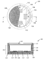
도 10은 몇몇 실시양태에 따른 두께가 약 350㎚±약 1.4%인 균일한 이산화티탄 코팅을 도시한 도면;
도 11은 본 발명의 실시양태에 따른 발광 디바이스의 도식적 단면도를 도시한 도면;
도 12는 본 발명의 실시양태에 따른 발광 디바이스의 평면도 및 단면도를 도시한 도면;
도 13 및 도 14는 본 발명의 실시양태에 따른 광발광 파장 전환 부품의 도식적 표시를 도시한 도면.1 illustrates a comparison of the intensity of luminescence between a coated green silicate phosphor and an uncoated green silicate phosphor according to some embodiments;
Figure 2 illustrates a comparison of the photoluminescent intensities between a coated green silicate phosphor and an uncoated green silicate phosphor according to some embodiments;
Figure 3 illustrates a comparison of photoluminescence intensities between a coated red nitride phosphor and an uncoated red nitride phosphor according to some embodiments;
Figure 4 illustrates the relative intensity of light for a green silicate phosphor according to some embodiments in time intervals greater than 1000 hours;
FIG. 5 illustrates relative chromaticity shift (CIE delta-x) over a time interval of more than 1000 hours for a green silicate phosphor according to some embodiments; FIG.
Figure 6 illustrates relative chromaticity shift (CIE delta-y) over a time interval of more than 1000 hours for a green silicate phosphor according to some embodiments;
Figure 7 illustrates the relative intensity of light for a red nitride phosphor according to some embodiments in time intervals greater than 1000 hours;
FIG. 8 illustrates relative chromaticity shift (CIE delta-x) over a time interval of more than 1000 hours for a nitride phosphor according to some embodiments;
Figure 9 illustrates relative chromaticity shift (CIE delta-y) over a time interval of 1000 hours for a nitride phosphor according to some embodiments;
Figure 10 illustrates a uniform titanium dioxide coating having a thickness of about 350 nm ± about 1.4% according to some embodiments;
11 is a schematic cross-sectional view of a light emitting device according to an embodiment of the present invention;
12 is a top view and a cross-sectional view of a light emitting device according to an embodiment of the present invention;
13 and 14 are diagrams showing a schematic representation of a photoluminescence wavelength conversion part according to an embodiment of the present invention;
본 명세서에 제공된 교시내용은 열 및 수분에 더 우수한 안정성을 보유하는 광발광 재료에 관한 것이다. 본 교시내용은 동일한 조성물의 비코팅 광발광 재료와 비교할 때, 예를 들면 수분 및 열에 더 우수한 안정성을 일반적으로 갖는 코팅된 광발광 재료를 포함한다. 코팅된 광발광 재료의 더 우수한 안정성은 예를 들면 발광 디바이스에서 재료의 광발광 성능의 안정성을 개선한다.The teachings provided herein relate to photoluminescent materials that have better stability to heat and moisture. The present teachings include coated photoluminescent materials that generally have better stability to, for example, moisture and heat when compared to uncoated photoluminescent materials of the same composition. The better stability of the coated photoluminescent material improves the stability of the photoluminescent performance of the material, for example in a light emitting device.
그러므로, 본 교시내용은 이산화티탄의 두꺼운 균일한 코팅을 갖는 신뢰성 있는 광발광 재료에 관한 것이다. 이 코팅된 재료는 광발광 재료 및 이 광발광 재료의 표면 위의 산화티탄을 포함하는 층을 포함하고, 층은 두께가 약 80㎚ 내지 약 500㎚, 약 80㎚ 내지 약 450㎚, 약 100㎚ 내지 약 400㎚, 약 125㎚ 내지 약 450㎚, 약 150㎚ 내지 약 375㎚, 약 175㎚ 내지 약 350㎚, 약 200㎚ 내지 약 400㎚, 약 250㎚ 내지 약 500㎚, 또는 이들 내의 임의의 범위이다. 몇몇 실시양태에서, 코팅 두께는 약 80㎚, 약 100㎚, 약 120㎚, 약 140㎚, 약 160㎚, 약 180㎚, 약 200㎚, 약 220㎚, 약 240㎚, 약 260㎚, 약 280㎚, 약 300㎚, 약 320㎚, 약 340㎚, 약 360㎚, 약 380㎚, 약 400㎚, 약 420㎚, 약 440㎚, 약 460㎚, 약 480㎚, 약 500㎚, 또는 이들 내의 약 5㎚ 증분의 임의의 두께일 수 있다.Therefore, the present teachings relate to reliable photoluminescent materials having a thick, uniform coating of titanium dioxide. The coated material includes a photoluminescent material and a layer comprising titanium oxide on the surface of the photoluminescent material, wherein the layer has a thickness of from about 80 nm to about 500 nm, from about 80 nm to about 450 nm, from about 100 nm From about 150 nm to about 375 nm, from about 175 nm to about 350 nm, from about 200 nm to about 400 nm, from about 250 nm to about 500 nm, or any within thereof Range. In some embodiments, the coating thickness is about 80 nm, about 100 nm, about 120 nm, about 140 nm, about 160 nm, about 180 nm, about 200 nm, about 220 nm, about 240 nm, About 300 nm, about 320 nm, about 340 nm, about 360 nm, about 380 nm, about 400 nm, about 420 nm, about 440 nm, about 460 nm, about 480 nm, about 500 nm, Lt; RTI ID = 0.0 > 5 nm < / RTI >
본 명세서에 교시된 코팅은 광발광 재료의 광 생성에 거의 영향을 미치지 않거나 영향이 없다. 예를 들면, 비코팅 형태의 광발광 재료로부터의 광발광의 강도 및 색도는 이산화티탄을 포함하는 층을 갖는 광발광 재료로부터의 광발광 강도와 동일하거나 실질적으로 동일할 수 있다.The coating taught herein has little or no effect on the photogeneration of the photoluminescent material. For example, the intensity and chromaticity of the photoluminescence from the photoluminescent material in the uncoated form may be the same or substantially the same as the photoluminescent intensity from the photoluminescent material with the layer comprising titanium dioxide.
몇몇 실시양태에서, 재료 사이에 예를 들면 휘도 안정성, 색상 안정성의 측정치 또는 이들의 조합을 사용하여 성능 신뢰성을 비교할 때, 비교 중인 상이한 광발광 재료를 포함하는 발광 디바이스 사이에서(발광 디바이스는 그 외에는 동일함), 광발광 코팅된 재료의 성능 매개변수의 신뢰성은 동일한 조성물의 비코팅 광발광 재료보다 클 수 있다. 다른 실시양태에서, 광발광, 휘도 안정성 또는 색상 안정성은 다른 코팅된 광발광 재료보다 크다. 용어 "안정성"은 예를 들면 일정 시간 동안 성능 매개변수의 열화 또는 변화에 대한 저항, 예컨대 일정 시간 동안 발광 디바이스의 출력 강도 또는 출력 일관성을 의미하기 위해 사용될 수 있다. 몇몇 실시양태에서, 일정 시간 기간은 발광 디바이스 내의 또는 사이의 성능 매개변수의 성능 신뢰성을 비교하기 위해 사용되는 일련의 조작 또는 시험 조건 하에, 예를 들면 1000시간, 1250시간, 1500시간, 1750시간, 2000시간, 3000시간, 4000시간, 5000시간, 또는 10,000시간일 수 있다.In some embodiments, when comparing performance reliability using, for example, a luminance stability, a measure of color stability, or a combination thereof, between materials, between light emitting devices comprising different light emitting materials being compared The reliability of the performance parameters of the photoluminescent coated material can be greater than the uncoated photoluminescent material of the same composition. In another embodiment, photoluminescence, brightness stability or color stability is greater than other coated photoluminescent materials. The term "stability" can be used to mean, for example, resistance to deterioration or change in performance parameters for a period of time, e.g., output intensity or output consistency of a light emitting device for a period of time. In some embodiments, the constant time period may be, for example, 1000 hours, 1250 hours, 1500 hours, 1750 hours, or even 1000 hours under a series of operating or test conditions used to compare the performance reliability of performance parameters within or between light emitting devices. 2000 hours, 3000 hours, 4000 hours, 5000 hours, or 10,000 hours.
이산화티탄 층을 균일한 또는 실질적으로 균일한 층으로서 증착시킬 수 있다. 당업자에게 공지된 임의의 측정치, 예컨대 본 명세서에 교시된 코팅에서의 측정으로부터 얻은 데이터의 통계 측정치를 이용하여 균일성을 표시할 수 있다. 예를 들면, 층의 균일성 변동이 의도되는 광발광 재료를 보호하는 층의 능력에 거의 영향을 미치지 않거나 영향이 없는 것으로 생각될 때, 층은 "균일"한 것으로 생각될 수 있다. 층의 균일성 변동이 의도되는 광발광 재료를 보호하는 층의 능력에 실질적인 영향을 더 적게 미쳐 성능 매개변수, 또는 성능 신뢰성에 오직 적은 영향을 미치는 것으로 생각되고, 디바이스의 사용자가 층이 적어도 실질적으로 의도되는 디바이스의 신뢰성을 증대시킨다고 믿을 때, 층은 "실질적으로 균일"한 것으로 생각될 수 있다.The titanium dioxide layer can be deposited as a uniform or substantially uniform layer. Any measurements known to those skilled in the art, such as statistical measurements of data obtained from measurements in the coatings taught herein, can be used to indicate uniformity. For example, a layer may be considered "homogeneous " when the uniformity variation of the layer is thought to have little or no effect on the ability of the layer to protect the intended photoluminescent material. It is believed that the uniformity of the layer variation is less likely to have a substantial effect on the ability of the layer to protect the photoluminescent material that is intended to affect only the performance parameter or performance reliability, When believed to increase the reliability of the intended device, the layer may be considered to be "substantially uniform ".
몇몇 실시양태에서, 용어 "실질적인"은 추구하는 것과 실현되는 것 사이의 차이를 나타내기 위해 사용될 수 있다. 몇몇 실시양태에서, 그 차이는 10%, 20%, 30%, 또는 35% 초과 또는 이들 사이의 임의의 양일 수 있고, 실질적인 것으로 생각될 수 없는 그 차이의 양은 고려 중인 측정치에 따라 달라질 수 있다. 예를 들면, 성능 특성이 적어도 추구하는 최저 정도를 만족시키지 않을 때, 변화가 실질적일 수 있다. 마찬가지로, 용어 "약"은 몇몇 실시양태에서 양 또는 변수를 의미하기 위해 사용될 수 있고, 양 또는 변수의 측정 시 차이는 관련 성능 특성의 실질적인 변화를 적게 생성할 때 그 차이는 실질적인 것으로 생각될 수 없다.In some embodiments, the term "substantial" can be used to denote the difference between seeking and being realized. In some embodiments, the difference can be any amount between 10%, 20%, 30%, or 35% or more between, and the amount of the difference that can not be considered substantial can vary depending on the measurement under consideration. For example, when the performance characteristic does not satisfy at least the minimum seeking, the change may be substantial. Likewise, the term "about" can be used to denote a quantity or variable in some embodiments, and the difference in the measurement of a quantity or a variable can not be regarded as substantial when producing a substantial change in the relevant performance characteristic .
광발광 재료의 표면에 도포된 층의 평균 두께로부터 변동 퍼센트를 사용하여 층의 균일성을 측정하고 비교할 수 있다. 두께 변동 퍼센트는, 예를 들면 약 1% 내지 약 33% 및 이들 내의 임의의 1% 증분 범위일 수 있고, 몇몇 실시양태에서, 층의 최소 두께는 80㎚ 이상이다. 몇몇 실시양태에서, 이산화티탄 층의 두께는 2% 미만으로 변한다. 다른 실시양태에서, 이산화티탄 층의 두께는 약 2%로 변한다. 또 다른 실시양태에서, 이산화티탄 층의 두께는 약 2.0% 내지 약 2.8%, 또는 이들 사이의 임의의 0.2% 증분으로 변한다. 또 다른 실시양태에서, 이산화티탄 층의 두께는 3% 미만으로 변한다. 또 다른 실시양태에서, 이산화티탄 층의 두께는 4% 미만으로 변한다. 또 다른 실시양태에서, 이산화티탄 층의 두께는 5% 미만으로 변한다. 또 다른 실시양태에서, 이산화티탄 층의 두께는 10% 미만으로 변한다. 또 다른 실시양태에서, 이산화티탄 층의 두께는 약 1.0% 내지 약 10.0%, 또는 이들 사이의 임의의 0.5% 증분으로 변한다. 또 다른 실시양태에서, 이산화티탄 층의 두께는 20% 미만으로 변한다. 또 다른 실시양태에서, 이산화티탄 층의 두께는 30% 미만으로 변한다. 변동 퍼센트가 허용되는 양을 초과할 때, 코팅 층은 또한 허용되는 두께보다 좁아져서, 광발광 재료에 예를 들면 수분으로부터 덜 바람직한 장벽을 제공할 수 있는 것으로 이해되어야 한다.The uniformity of the layer can be measured and compared using the percentage variation from the average thickness of the applied layer to the surface of the photoluminescent material. The percent thickness variation may be, for example, from about 1% to about 33% and any 1% increments within them, and in some embodiments, the minimum thickness of the layer is at least 80 nm. In some embodiments, the thickness of the titanium dioxide layer varies to less than 2%. In another embodiment, the thickness of the titanium dioxide layer changes to about 2%. In another embodiment, the thickness of the titanium dioxide layer varies from about 2.0% to about 2.8%, or any 0.2% increment therebetween. In another embodiment, the thickness of the titanium dioxide layer changes to less than 3%. In another embodiment, the thickness of the titanium dioxide layer is changed to less than 4%. In another embodiment, the thickness of the titanium dioxide layer changes to less than 5%. In another embodiment, the thickness of the titanium dioxide layer changes to less than 10%. In another embodiment, the thickness of the titanium dioxide layer varies from about 1.0% to about 10.0%, or any 0.5% increment therebetween. In another embodiment, the thickness of the titanium dioxide layer changes to less than 20%. In another embodiment, the thickness of the titanium dioxide layer changes to less than 30%. It should be understood that when the percentage of variation exceeds an allowable amount, the coating layer can also be narrower than the thickness allowed to provide a less desirable barrier to the photoluminescent material, for example, from moisture.
허용되는 양의 변동은 코팅의 평균 두께에 따라 다랄진다. 몇몇 실시양태에서, 허용되는 양의 변동은 코팅 층에서 80㎚ 초과의 최소 두께를 발생시키는 것이다. 그러므로, 용어 "균일성"은 예를 들면 전자 현미경검사와 같은 당업자에게 공지된 임의의 방법을 이용하여 측정된 두께 변동과 관련하여 사용될 수 있다. 몇몇 실시양태에서, 두께 변동은 ±5㎚, ±10nm, ±15㎚, ±20㎚, ±25 nm, ±30㎚, ±35㎚, ±40㎚, ±45㎚, ±50㎚, ±60㎚, ±70㎚, ±80㎚, ±90㎚, 또는 ±100㎚일 수 있다. 몇몇 실시양태에서, 변동은 30㎚, 20㎚, 10㎚, 5㎚, 3㎚, 2㎚, 또는 1㎚ 미만이다. 몇몇 실시양태에서, 변동은 ±5%, ±10%, ±15%, ±20%, ±25%, ±30%, 또는 ±35%일 수 있다. 몇몇 실시양태에서, 변동은 30%, 20%, 10%, 5%, 3%, 2%, 또는 1% 미만이다.The amount of variation allowed depends on the average thickness of the coating. In some embodiments, an acceptable amount of variation results in a minimum thickness of greater than 80 nm in the coating layer. Therefore, the term "uniformity" can be used in connection with measured thickness variations using any method known to those skilled in the art, such as, for example, electron microscopy. In some embodiments, the thickness variation may be in the range of ± 5 nm, ± 10 nm, ± 15 nm, ± 20 nm, ± 25 nm, ± 30 nm, ± 35 nm, ± 40 nm, ± 45 nm, ± 50 nm, ± 60 nm , ± 70 nm, ± 80 nm, ± 90 nm, or ± 100 nm. In some embodiments, the variation is less than 30 nm, 20 nm, 10 nm, 5 nm, 3 nm, 2 nm, or 1 nm. In some embodiments, the variation can be ± 5%, ± 10%, ± 15%, ± 20%, ± 25%, ± 30%, or ± 35%. In some embodiments, the variation is less than 30%, 20%, 10%, 5%, 3%, 2%, or 1%.
몇몇 실시양태에서, 이산화티탄 층은 두께가 약 80㎚ 내지 약 500㎚일 수 있다. 다른 실시양태에서, 이산화티탄 층은 두께가 약 100㎚ 내지 약 500㎚일 수 있다. 또 다른 실시양태에서, 이산화티탄 층은 두께가 약 200㎚ 내지 약 500㎚일 수 있다. 또 다른 실시양태에서, 이산화티탄 층은 두께가 약 400㎚ 내지 약 500㎚일 수 있다. 또 다른 실시양태에서, 이산화티탄 층은 두께가 약 200㎚ 내지 약 400㎚일 수 있다. 또 다른 실시양태에서, 이산화티탄 층은 두께가 약 300㎚ 내지 약 400㎚일 수 있다. 또 다른 실시양태에서, 이산화티탄 층은 두께가 약 350㎚일 수 있다. 몇몇 실시양태에서, 이산화티탄 층은 두께가 약 100㎚, 200㎚, 300㎚, 400㎚, 500㎚, 또는 이들 사이의 임의의 10㎚ 증분일 수 있다.In some embodiments, the titanium dioxide layer may have a thickness of from about 80 nm to about 500 nm. In another embodiment, the titanium dioxide layer may have a thickness of from about 100 nm to about 500 nm. In another embodiment, the titanium dioxide layer may have a thickness of from about 200 nm to about 500 nm. In another embodiment, the titanium dioxide layer may have a thickness of from about 400 nm to about 500 nm. In another embodiment, the titanium dioxide layer may have a thickness of from about 200 nm to about 400 nm. In another embodiment, the titanium dioxide layer may have a thickness of from about 300 nm to about 400 nm. In another embodiment, the titanium dioxide layer may be about 350 nm thick. In some embodiments, the titanium dioxide layer may be about 10 nm increments in thickness between about 100 nm, 200 nm, 300 nm, 400 nm, 500 nm, or the like.
몇몇 실시양태에서, 코팅된 재료의 크기는 약 2㎛ 내지 약 50㎛이다. 다른 실시양태에서, 코팅된 재료의 크기는 약 5㎛ 내지 약 20㎛이다. 당업자에게 공지된 임의의 방법을 이용하여 코팅된 재료의 크기를 결정할 수 있다.In some embodiments, the size of the coated material is from about 2 [mu] m to about 50 [mu] m. In another embodiment, the size of the coated material is from about 5 [mu] m to about 20 [mu] m. Any method known to those skilled in the art can be used to determine the size of the coated material.
몇몇 실시양태에서, 광발광 재료는 인광체이다. 다른 실시양태에서, 광발광 재료는 규산염 인광체, 알루민산염 인광체, 질화물 인광체, 산화질화물 인광체, 황화물 인광체 또는 산화황화물 인광체이다. 또 다른 실시양태에서, 광발광 재료는 규산염 인광체이다.In some embodiments, the photoluminescent material is a phosphor. In another embodiment, the photoluminescent material is a silicate phosphor, an aluminate phosphor, a nitride phosphor, an oxynitride phosphor, a sulfide phosphor, or an oxidized sulfide phosphor. In another embodiment, the photoluminescent material is a silicate phosphor.
몇몇 실시양태에서, 인광체는 예를 들면 (Ca, Sr, Ba)(Al, In, Ga)2S4:Eu, (Ca, Sr)S:Eu, CaS:Eu, (Zn, Cd)S:Eu:Ag와 같은 황화물 인광체이다. 다른 실시양태에서, 인광체는 예를 들면 (Ca, Sr, Ba)2Si5N8:Eu, CaAlSiN3:Eu, Ce(Ca, Sr, Ba)Si7N10:Eu 또는 (Ca, Sr, Ba)SiN2:Eu와 같은 질화물 인광체이다. 다른 예시적인 인광체는 Ba2 +, Mg2 + 동시도핑된 Sr2SiO4, (Y, Gd, Lu, Sc, Sm, Tb, Th, Ir, Sb, Bi)3(Al, Ga)5O12:Ce(Pr과 함께 또는 이것 없이), YSiO2N:Ce, Y2Si3O3N4:Ce, Gd2Si3O3N4:Ce, (Y, Gd, Tb, Lu)3Al5 - xSixO12 -x:Ce, BaMgAl10O17:Eu(Mn과 함께 또는 이것 없이), SrAl2O4:Eu, Sr4A14O25:Eu, (Ca, Sr, Ba)Si2N2O2:Eu, SrSi,Al2O3N2:Eu, (Ca, Sr, Ba)Si2N2O2:Eu, (Ca, Sr, Ba)SiN2:Eu 및 (Ca, Sr, Ba)SiO4:Eu(Winkler et al, 미국 특허 출원 제2010/0283076호; Lee 외, Applied Surface Science 257, (2011) 8355-8369)를 포함한다.In some embodiments, the phosphor, for example, (Ca, Sr, Ba) ( Al, In, Ga) 2 S 4: Eu, (Ca, Sr) S: Eu, CaS: Eu, (Zn, Cd) S: Eu: Ag is a sulfide phosphor such as Ag. (Ca, Sr, Ba) 2 Si 5 N 8 : Eu, CaAlSiN 3 : Eu, Ce (Ca, Sr, Ba) Si 7 N 10 : Eu, Ba) SiN 2 : Eu. Other exemplary phosphor is Ba 2 +, Mg 2 + co-doped Sr 2 SiO 4, (Y, Gd, Lu, Sc, Sm, Tb, Th, Ir, Sb, Bi) 3 (Al, Ga) 5 O 12 : Ce (Pr and with or without it), YSiO 2 N: Ce,
몇몇 실시양태에서, 인광체는 화학식 (Sr1-x-yMxTy)3-mEum(Si1-zAlz)O5(여기서, M은 Ba, Mg 및 Zn 중 적어도 1종이고, T는 3가 금속이며, 0≤x≤0.4이고, 0≤y≤0.4이며, 0≤z≤0.2이고, 0.001≤m≤0.4임)의 혼합 2가 및 3가 양이온을 갖는 알루미늄-규산염계 오렌지색-적색 인광체이다(Liu 외, 미국 특허 출원 제2008/0111472호).In some embodiments, the phosphor has the formula (Sr 1-xy M x T y) 3-m Eu m (Si 1-z Al z) O 5 ( wherein, at least one member of the M is Ba, Mg and Zn and, T Silicate-based orange-yellowish-yellowish-yellowish-yellowish-yellowish-yellowish-yellowish-yellowish-yellowish- Red phosphor (Liu et al., U. S. Patent Application No. 2008/0111472).
다른 실시양태에서, 인광체는 화학식 (Y, A)3(Al, B)5(O, C)12:Ce3 +(여기서, A는 Tb, Gd, Sm, La, Sr, Ba, Ca로 이루어진 군으로부터 선택되고, A는 약 0.1% 내지 100% 범위의 양으로 Y를 치환하고; B는 Si, Ge, B, P 및 Ga로 이루어진 군으로부터 선택되고, B는 약 0.1% 내지 100% 범위의 양으로 Al을 치환하고; C는 F, Cl, N 및 S로 이루어진 군으로부터 선택되고, C는 0.1% 내지 100% 범위의 양으로 O를 치환함)의 YAG:Ce 인광체이다(Tao 외, 미국 특허 출원 제2008/0138268호).In another embodiment, the phosphor has the formula (Y, A) 3 (Al , B) 5 (O, C) 12: Ce 3 + ( where, A is composed of Tb, Gd, Sm, La, Sr, Ba, Ca B is selected from the group consisting of Si, Ge, B, P, and Ga, and B is selected from the group consisting of about 0.1% to 100% (Wherein C is selected from the group consisting of F, Cl, N and S and C is substituted by O in an amount ranging from 0.1% to 100%) (Tao et al., USA Patent Application No. 2008/0138268).
또 다른 실시양태에서, 인광체는 화학식 A2SiO4:Eu2+D(여기서, A는 Sr, Ca, Ba, Mg, Zn 및 Cd이고; D는 F, Cl, Br, I, P, S 및 N으로 이루어진 군으로부터 선택되는 도펀트임)의 규산염계 황색-녹색 인광체이다(Wang 외, 미국 특허 제7,311,858호).In another embodiment, the phosphor is represented by the formula A 2 SiO 4 : Eu 2+ D, where A is Sr, Ca, Ba, Mg, Zn and Cd; D is F, Cl, Br, I, N, which is a silicate-based yellow-green phosphor (Wang et al., U.S. Patent No. 7,311,858).
또 다른 실시양태에서, 인광체는 화학식 (M1-xEux)2-zMgzAly)O(2+3/2)y(여기서, M은 Ba 및 Sr 중 적어도 1종이고, (0.05<x<0.5; 3≤y≤8; 및 0.8≤z≤l<1.2) 또는 (0.2<x<0.5; 3≤y≤8; 및 0.8≤z≤l<1.2) 또는 (0.05<x<0.5; 3≤y≤12; 및 0.8≤z≤l<1.2) 또는 (0.2<x<0.5; 3≤y≤12; 및 0.8≤z≤l<1.2) 또는 (0.05<x<0.5; 3≤y≤6; 및 0.8≤z≤1.2)임)의 알루민산염계 청색 인광체이다(Dong 외, 미국 특허 제7,390,437호).In another embodiment, the phosphor and the formula (M 1-x Eu x) 2-z Mg z Al y) O (2 + 3/2) y ( where, at least one member of the M is selected from Ba and Sr, (0.05 (0.2 < x < 0.5, 3 y < 8 and 0.8 z < l & X? 0.5? 3? Y? 12 and 0.8? Z? L <1.2) or (0.05 <x <0.5; ? 6; and 0.8? Z? 1.2). (Dong et al., U.S. Patent No. 7,390,437).
또 다른 실시양태에서, 인광체는 화학식 (Gd1 - xAx)(V1 - yBy)(O4 - zCz)(여기서, A는 Bi, Tl, Y, La, Ce, Pr, Nd, Pm, Sm, Eu, Tb, Dy, Ho, Er, Tm, Yb, Lu이고; B는 Ta, Nb, W, 및 Mo이며; C는 N, F, Br 및 I이고; 0<x<0.2이며; 0<y<0.1이고; 0<z<0.1임)의 황색 인광체이다(Li 외, 미국 특허 제7,399,428호). In another embodiment, the phosphor has the formula (Gd 1 - x A x) (V 1 - y B y) (O 4 - z C z) ( where, A is Bi, Tl, Y, La, Ce, Pr, B, Ta, Nb, W and Mo; C is N, F, Br and I; 0 < x <0.2; 0 <y <0.1 and 0 <z <0.1) (Li et al., US Pat. No. 7,399,428).
또 다른 실시양태에서, 인광체는 화학식 A[Srx(M1)1-x]zSiO4ㆍ(1-a)[Sry(M2)1-y]uSiO5:Eu2+D(여기서, M1 및 M2는 Ba, Mg, Ca, 및 Zn과 같은 2가 금속 중 적어도 1종이고; 0.6≤a≤0.85이며; 0.3≤x≤0.6이고; 0.85≤y≤1이며; 1.5≤z≤2.5이고; 2.6<u<3.3이며, Eu 및 D는 0.0001 내지 약 0.5이고; D는 F, Cl, Br, S 및 N으로 이루어진 군으로부터 선택되는 음이온이며, D 중 적어도 몇몇은 임자 격자 내에 산소를 대체함)의 황색 인광체이다(Li 외, 미국 특허 제7,922,937호).In another embodiment, the phosphor has the formula A [Sr x (M 1) 1-x]
또 다른 실시양태에서, 인광체는 화학식 (Sr, A1)x(Si, A2)(O, A3)2+x:Eu2 +(여기서, A1은 Mg, Ca, Ba, Zn 또는 +1 및 =3 이온의 조합과 같은 적어도 1종의 2가 금속 이온이고; A2는 B, Al, Ga, C, Ge, P 중 적어도 1종을 포함하는 3+, 4+ 또는 5+ 양이온이며; A3은 F, Cl, 및 Br을 포함하는 1-, 2- 또는 3- 음이온이고; 1.5<x<2.5임)의 규산염계 녹색 인광체이다(Li 외, 미국 특허 출원 제2009/0294731호). In another embodiment, the phosphor has the formula (Sr, A 1) x ( Si, A 2) (O, A 3) 2 + x:
또 다른 실시양태에서, 인광체는 화학식 MaMbBc(N, D):Eu2 +(여기서, Ma는 Mg, Ca, Sr, Ba와 같은 2가 금속 이온이고; Mb는 Al, Ga, Bi, Y, La, Sm과 같은 3가 금속이며; Mc는 Si, Ge, Pl, 및 B와 같은 3가 원소이고; N은 질소이고; D는 F, Cl 또는 Br과 같은 할로겐임)의 질화물계 적색 인광체이다(Liu 외, 미국 특허 출원 제2009/0283721호).In another embodiment, the phosphor has the formula M a M b B c (N , D):
또 다른 실시양태에서, 인광체는 화학식 (Sr, A1)x(Si, A2)(O, A3)2+x:Eu2 +(여기서, A1은 Mg, Ca, Ba, Zn 또는 +1 및 =3 이온의 조합과 같은 적어도 1종의 2가 금속 이온이고; A2는 B, Al, Ga, C, Ge, P 중 적어도 1종을 포함하는 3+, 4+ 또는 5+ 양이온이며; A3은 F, Cl, 및 Br을 포함하는 1-, 2- 또는 3- 음이온이고; 1.5<x<2.5임)의 규산염계 오렌지색 인광체이다(Cheng 외, 미국 특허 제7,655, 156호).In another embodiment, the phosphor has the formula (Sr, A 1) x ( Si, A 2) (O, A 3) 2 + x:
또 다른 실시양태에서, 인광체는 화학식 M1-xEuxMg1-yMnyAlzO[(x+y)+3z/2)](여기서, 0.1<x<1.0이고; 0.1<y<1.0이며; 0.2<x+y<2.0이고; 2≤z≤14임)의 알루민산염계 녹색 인광체이다(Wang 외, 미국 특허 제7,755,276호).In another embodiment, the phosphor is represented by the formula M 1-x Eu x Mg 1 -y Mn y Al z O [(x + y) + 3z / 2)] where 0.1 <x < 1.0 and 0.2 < x + y < 2.0 and 2? Z? 14) (Wang et al., U.S. Patent No. 7,755,276).
본 명세서에 제공된 교시내용은, 예를 들면 본 명세서에 기재된 것과 같은 임의의 다양한 광발광 기재 위의 이산화티탄을 포함하는 코팅의 도포에 관한 것이다. 몇몇 실시양태에서, 이산화티탄은 이산화티탄 전구체로부터 생성될 수 있다. 몇몇 실시양태에서, 전구체는 유기 금속 화합물이다. 다른 실시양태에서, 유기 금속 화합물은 티탄 에톡사이드(Ti(EtO)4), 티탄 프로폭사이드(Ti(PrO)4), 티탄 아이소프로폭사이드(Ti(i-PrO)4), 티탄 n-뷰톡사이드(Ti(n-BuO)4), 티탄 아이소-뷰톡사이드(Ti(i-BuO)4), 티탄 tert-뷰톡사이드(Ti(i-BuO)4), 테트라키스(다이에틸아미노)티탄[(CH3CH2)2N]4, Ti(AcAc)4, Ti(CH3)4, Ti(C2H5)4 또는 이들의 조합이다. 몇몇 실시양태에서, 전구체는 무기 염이다. 다른 실시양태에서, 무기 염은 산화티탄(TiO2), 염화티탄(TiCl4), 불화티탄(TiF4), 질산티탄(Ti(NO3)4), 브롬화티탄(TiBr4), 요오드화티탄(TiI4) 또는 황산티탄(TiOSO4)이다.The teachings provided herein relate, for example, to the application of coatings comprising titanium dioxide on any of a variety of photoluminescent substrates such as those described herein. In some embodiments, the titanium dioxide can be produced from a titanium dioxide precursor. In some embodiments, the precursor is an organometallic compound. In another embodiment, the organic metal compound is titanium ethoxide (Ti (EtO) 4), titanium propoxide (Ti (PrO) 4), titanium isopropoxide (Ti (i-PrO) 4 ), titanium n- butoxide (Ti (n-BuO) 4 ), titanium iso-butoxide (Ti (i-BuO) 4 ), titanium tert- butoxide (Ti (i-BuO) 4 ), tetrakis (diethylamino) titanium [(CH 3 CH 2) 2 N] 4, Ti (AcAc) 4, Ti (CH 3) 4, Ti (C 2 H 5) 4 or a combination thereof. In some embodiments, the precursor is an inorganic salt. In another embodiment, the inorganic salt is selected from the group consisting of titanium oxide (TiO 2 ), titanium chloride (TiCl 4 ), titanium fluoride (TiF 4 ), titanium nitrate (Ti (NO 3 ) 4 ), titanium bromide (TiBr 4 ), titanium iodide a TiI 4), or titanium sulfate (TiOSO 4).
본 명세서의 교시내용은 또한 열 및 수분에 더 우수한 안정성을 보유하는 광발광 재료의 제조 방법을 제공한다. 몇몇 실시양태에서, 상기 방법은 단일 코팅 사이클로 광발광 재료 위에 적어도 약 80㎚의 두께의 균일한 이산화티탄 층을 증착시키기에 효과적인 시간 동안 이산화티탄을 증착시키는 단계를 포함할 수 있다. 몇몇 실시양태에서, 상기 방법은 광발광 재료의 표면 위에 이산화티탄 층을 증착시키는 단계를 포함하고, 이산화티탄은 액상 중의 이산화티탄 전구체로부터 생성될 수 있다. 단일 코팅 사이클로 광발광 재료의 표면 위에 적어도 약 80㎚의 원하는 두께로 이산화티탄의 균일한 층을 생성하기에 효과적인 시간 동안 증착이 일어날 수 있다. 몇몇 실시양태에서, 상기 방법은 전구체와 용매의 혼합물을 형성하는 단계, 및 (i) 전구체로부터의 이산화티탄의 형성 속도 및 (ii) 균일한 층을 증착시키기에 효과적인 시간 동안 광발광 재료의 표면 위의 이산화티탄의 증착 속도를 제어하기 위해 혼합물에 물을 점진적으로 첨가하는 단계를 포함한다. 몇몇 실시양태에서, 용매는 물; 알콜, 예컨대 메탄올, 에탄올, 프로판올, 아이소프로판올, 뷰탄올, 펜탄올, 및 헥산올; 아세톤; 메틸 에틸 케톤; 다른 탄화수소; 또는 이들의 혼합물을 포함할 수 있다.The teachings herein also provide a method of making a photoluminescent material that has better stability to heat and moisture. In some embodiments, the method may comprise depositing titanium dioxide over a period of time effective to deposit a uniform layer of titanium dioxide on the photoluminescent material in a single coating cycle, the thickness of the layer being at least about 80 nm thick. In some embodiments, the method comprises depositing a layer of titanium dioxide on the surface of the photoluminescent material, wherein the titanium dioxide can be generated from the titanium dioxide precursor in the liquid phase. Deposition can take place over a period of time effective to produce a uniform layer of titanium dioxide with a desired thickness of at least about 80 nm on the surface of the photoluminescent material with a single coating cycle. In some embodiments, the method comprises forming a mixture of a precursor and a solvent, and forming a mixture of the precursor and the solvent on the surface of the photoluminescent material for a time effective to (i) form a titanium dioxide from the precursor and (ii) And gradually adding water to the mixture to control the deposition rate of titanium dioxide. In some embodiments, the solvent is water; Alcohols such as methanol, ethanol, propanol, isopropanol, butanol, pentanol, and hexanol; Acetone; Methyl ethyl ketone; Other hydrocarbons; Or mixtures thereof.
몇몇 실시양태에서, 코팅된 광발광 재료를 합성하는 방법은 광발광 재료를 용매에 첨가하여 제1 혼합물을 형성하는 단계; 이산화티탄 전구체의 가수분해에 준비하기 위해 제1 혼합물의 pH를 조정하는 단계; 이산화티탄 전구체를 제1 혼합물에 첨가하여 제2 혼합물을 형성하는 단계(여기서, 전구체는 제1 혼합물에 제어된 속도로 첨가될 수 있고, 첨가되는 전구체의 양은 광발광 재료의 중량과 비교하여 이산화티탄의 약 10중량% 미만의 양일 수 있음); 광발광 재료의 표면 위의 이산화티탄의 증착을 허용하는 시간 동안 제2 혼합물을 혼합하는 단계; 코팅된 광발광 재료를 세척하는 단계; 코팅된 광발광 재료를 정제하는 단계; 코팅된 광발광 재료를 건조시키는 단계; 및 코팅된 광발광 재료를 하소시키는 단계를 포함할 수 있다.In some embodiments, a method of synthesizing a coated photoluminescent material comprises: adding a photoluminescent material to a solvent to form a first mixture; Adjusting the pH of the first mixture to prepare for hydrolysis of the titanium dioxide precursor; Adding a titanium dioxide precursor to the first mixture to form a second mixture wherein the precursor can be added to the first mixture at a controlled rate and the amount of precursor added is less than the weight of the light- ≪ / RTI > less than about 10% by weight of the composition; Mixing the second mixture for a time allowing deposition of titanium dioxide on the surface of the photoluminescent material; Washing the coated photoluminescent material; Purifying the coated photoluminescent material; Drying the coated photoluminescent material; And calcining the coated photoluminescent material.
임의의 수의 추가의 단계를 공정에 추가할 수 있는 것으로 이해되어야 한다. 예를 들면, 코팅 공정은 추가의 반응 단계, 경화 단계, 건조 단계, 열 처리 단계 등을 포함할 수 있다. 예를 들면, 상기 공정은 물과 용매의 혼합물을 첨가하여 제3 "경화" 혼합물을 형성하는 단계; 제3 혼합물을 제2 시간 동안 가열 및/또는 반응시키는 단계; 및 가능하게는 추가의 단계를 제3 시간 동안 추가하는 단계를 포함할 수 있다. 몇몇 실시양태에서, 예를 들면 광발광 재료의 농도는 약 0.0001g/㎖ 내지 약 10.0g/㎖일 수 있다.It should be understood that any number of additional steps may be added to the process. For example, the coating process may include additional reaction steps, a curing step, a drying step, a heat treatment step, and the like. For example, the process may include adding a mixture of water and a solvent to form a third "cure" mixture; Heating and / or reacting the third mixture for a second time; And possibly adding an additional step for a third time. In some embodiments, for example, the concentration of the photoluminescent material may be from about 0.0001 g / ml to about 10.0 g / ml.
몇몇 실시양태에서, 본 명세서에 제공된 교시내용을 이용하여 표면 위의 이산화티탄의 증착 속도는 원자 층 증착 수준으로 제어될 수 있는 것으로 이해되어야 한다. 증착 속도는 반응 시간 선택에 이용될 수 있다. 당업자는 반응 시간 선택이 적어도 부분적으로 전구체, 시약 농도, 시약 첨가 속도, 반응 온도 및 원하는 코팅 두께의 선택을 포함할 수 있는 공정 설계에 따라 달라진다는 것을 이해할 것이다. 이 공정 조건은 광발광 재료의 표면 위의 이산화티탄의 증착 속도를 결정한다. 몇몇 실시양태에서, 이산화티탄은 시간당 약 1㎚ 내지 약 100㎚의 속도로 증착된다. 몇몇 실시양태에서, 이산화티탄은 시간당 약 5㎚ 내지 약 20㎚의 속도로 광발광 재료에 증착된다. 다른 실시양태에서, 이산화티탄은 시간당 약 3㎚ 내지 약 18nm의 속도로 광발광 재료에 증착된다. 또 다른 실시양태에서, 이산화티탄은 시간당 약 6nm 내지 약 15㎚의 속도로 광발광 재료에 증착된다. 또 다른 실시양태에서, 이산화티탄은 시간당 약 5nm 내지 약 7nm의 속도로 광발광 재료에 증착된다. 또 다른 실시양태에서, 제2 이산화티탄 층은 광발광 재료 위에 증착된다.In some embodiments, it should be understood that the deposition rate of titanium dioxide on the surface can be controlled to the atomic layer deposition level using the teachings provided herein. The deposition rate can be used to select the reaction time. Those skilled in the art will appreciate that the reaction time selection will depend, at least in part, on the process design, which may include the choice of precursor, reagent concentration, reagent addition rate, reaction temperature and desired coating thickness. This process condition determines the deposition rate of titanium dioxide on the surface of the photoluminescent material. In some embodiments, titanium dioxide is deposited at a rate of about 1 nm to about 100 nm per hour. In some embodiments, titanium dioxide is deposited on the photoluminescent material at a rate of about 5 nm to about 20 nm per hour. In another embodiment, the titanium dioxide is deposited on the photoluminescent material at a rate of about 3 nm to about 18 nm per hour. In another embodiment, the titanium dioxide is deposited on the photoluminescent material at a rate of about 6 nm to about 15 nm per hour. In another embodiment, titanium dioxide is deposited on the photoluminescent material at a rate of about 5 nm to about 7 nm per hour. In another embodiment, a second titanium dioxide layer is deposited over the photoluminescent material.
몇몇 실시양태에서, 반응물의 계량 첨가를 통해 농도를 제어할 수 있다. 예를 들면, 전구체를 용매 중에 희석하고 물을 전구체의 가수분해를 제어하기 위한 제어 속도로 첨가할 수 있다. 몇몇 실시양태에서, 전구체는 아이소프로판올 중에 Ti(i-PrO)4 용해될 수 있고, 물은 전구체의 가수분해를 제어하기 위한 제어 속도로 계량 첨가를 통해 점진적으로 첨가될 수 있다. 다른 예에서, 광발광 재료와 용매의 제1 혼합물을 원하는 pH로 조정하여 전구체의 가수분해에 준비할 수 있고, 이후 전구체의 가수분해를 제어하기 위한 제어 속도를 이용하여 전구체를 원하는 pH로 제1 혼합물에 첨가한다.In some embodiments, the concentration can be controlled by metered addition of the reactants. For example, the precursor may be diluted in a solvent and water added at a controlled rate to control the hydrolysis of the precursor. In some embodiments, the precursor can be dissolved Ti (i-PrO) 4 in isopropanol and water can be added incrementally through metering at a controlled rate to control the hydrolysis of the precursor. In another example, the first mixture of photoluminescent material and solvent may be adjusted to a desired pH to prepare for hydrolysis of the precursor, and then the precursor may be heated to a desired pH using a control rate to control the hydrolysis of the precursor Add to the mixture.
당업자에게 공지된 임의의 방법을 이용하여 반응물의 계량 첨가를 성취할 수 있다. 몇몇 실시양태에서, 전구체에 가수분해되는 조건을 포함하는 혼합물에 전구체를 적하할 수 있다. 몇몇 실시양태에서, 미세한 니들로 연속하여 전구체를 주입할 수 있다. 몇몇 실시양태에서, 가수분해제, 예컨대 물 또는 유기 용매 함유 물을 전구체와 용매의 혼합물에 적하할 수 있다. 예를 들면, 상기 방법은 전구체와 용매의 혼합물을 형성하는 단계, 및 (i) 전구체로부터의 이산화티탄의 형성 속도 및 (ii) 균일한 층을 증착시키기에 효과적인 시간 동안 광발광 재료의 표면 위의 이산화티탄의 증착 속도를 제어하기 위해 혼합물에 물을 점진적으로 첨가하는 단계를 포함할 수 있다.Any method known to those skilled in the art can be used to achieve metered addition of reactants. In some embodiments, a precursor may be added to a mixture comprising conditions that are hydrolyzed to the precursor. In some embodiments, a precursor can be injected in succession with a fine needle. In some embodiments, a hydrolytic release, such as a water or organic solvent inclusion, may be added to the mixture of precursor and solvent. For example, the method may include forming a mixture of a precursor and a solvent, and forming a mixture of (i) a rate of formation of titanium dioxide from the precursor and (ii) a time sufficient to deposit a uniform layer on the surface of the photoluminescent material And gradually adding water to the mixture to control the deposition rate of titanium dioxide.
몇몇 실시양태에서, 전구체를 약 0.0001㎖/분 내지 200㎖/분의 속도로 첨가할 수 있다. 몇몇 실시양태에서, 전구체를 약 2㎖/분 내지 30㎖/분의 속도로 첨가할 수 있다. 몇몇 실시양태에서, 전구체를 약 6㎖/분 내지 20㎖/분의 속도로 첨가할 수 있다. 몇몇 실시양태에서, 전구체를 약 5㎖/분 내지 60㎖/분의 속도로 첨가할 수 있다.In some embodiments, the precursor may be added at a rate of about 0.0001 ml / min to 200 ml / min. In some embodiments, the precursor may be added at a rate of about 2 ml / min to 30 ml / min. In some embodiments, the precursor may be added at a rate of about 6 ml / min to 20 ml / min. In some embodiments, the precursor may be added at a rate of about 5 ml / min to 60 ml / min.
증착 속도의 제어는 광발광 재료의 표면 위에 이산화티탄 층의 원하는 두께를 증착시키기 위한 반응 시간의 제어를 제공한다. 반응 시간은 예를 들면 0.1.0시간 내지 10일, 1.0시간 내지 7일, 2시간 내지 5일, 1.0시간 내지 4일, 0.5시간 내지 3일, 0.5시간 내지 2일, 0.5시간 내지 1일, 1.0시간 내지 18시간, 0.5시간 내지 12시간, 0.5시간 내지 8시간, 1.0시간 내지 6시간, 0.5시간 내지 4시간, 0.5시간 내지 2시간, 또는 이들 내의 임의의 범위일 수 있다.Control of the deposition rate provides control of the reaction time for depositing a desired thickness of the titanium dioxide layer on the surface of the photoluminescent material. The reaction time is, for example, 0.1.0 hours to 10 days, 1.0 hours to 7 days, 2 hours to 5 days, 1.0 hours to 4 days, 0.5 hours to 3 days, 0.5 hours to 2 days, 0.5 hours to 1 day, From 1.0 hour to 18 hours, from 0.5 hours to 12 hours, from 0.5 hours to 8 hours, from 1.0 hour to 6 hours, from 0.5 hours to 4 hours, from 0.5 hours to 2 hours, or any range within these ranges.
몇몇 실시양태에서, 반응 혼합물을 약 30℃ 내지 용매의 비점±10℃ 범위의 온도로 가열할 수 있다. 다른 실시양태에서, 반응 혼합물을 약 40℃ 내지 약 80℃의 온도로 가열할 수 있다. 용어 "반응한다", "반응하는" 및 "반응"은 몇몇 실시양태에서, 예를 들면 전구체를 가수분해하여 이산화티탄을 형성하는 것, 광발광 재료의 표면 위에 이산화티탄의 층을 증착시키는 것 등을 의미하는 것으로 이해되어야 하고, 공정에서 이 단계 동안 분자 구조 간의 결합 변화가 일어날 수 있다.In some embodiments, the reaction mixture can be heated to a temperature ranging from about 30 캜 to the boiling point of the solvent 賊 10 캜. In another embodiment, the reaction mixture can be heated to a temperature of about 40 캜 to about 80 캜. The term " reacts ", "reacting" and "reaction" include, in some embodiments, for example, hydrolysis of the precursor to form titanium dioxide, deposition of a layer of titanium dioxide on the surface of the photoluminescent material , And the bond change between molecular structures during this step in the process can occur.
몇몇 실시양태에서, 코팅된 광발광 재료를 정제할 수 있다. 예를 들면, 코팅된 광발광 재료를 용매로 첨가한 후, 여과하여 정제할 수 있다. 다른 실시양태에서, 코팅된 광발광 재료를 원심분리, 침강 및 경사여과에 의해 정제할 수 있다. 당업자에게 공지된 임의의 정제 방법을 사용할 수 있다.In some embodiments, the coated photoluminescent material can be purified. For example, the coated photoluminescent material can be added as a solvent and then purified by filtration. In another embodiment, the coated photoluminescent material can be purified by centrifugation, sedimentation and gradient filtration. Any purification method known to those skilled in the art can be used.
몇몇 실시양태에서, 코팅된 광발광 재료를 약 60℃ 내지 약 200℃의 온도에서 건조시킬 수 있다. 다른 실시양태에서, 코팅된 광발광 재료를 약 85℃ 내지 약 200℃의 온도에서 건조시킬 수 있다. 몇몇 실시양태에서, 건조는 진공 건조, 동결 건조, 또는 임계점 건조를 포함할 수 있다. 또 다른 실시양태에서, 코팅된 광발광 재료를 약 200℃ 내지 약 600℃의 온도에서 하소시킬 수 있다.In some embodiments, the coated photoluminescent material can be dried at a temperature from about 60 [deg.] C to about 200 < 0 > C. In another embodiment, the coated photoluminescent material can be dried at a temperature of from about 85 캜 to about 200 캜. In some embodiments, drying may include vacuum drying, freeze drying, or critical point drying. In another embodiment, the coated photoluminescent material can be calcined at a temperature from about 200 [deg.] C to about 600 < 0 > C.
코팅된 광발광 재료를 합성하는 다른 방법이 본 명세서에 제공된다. 광발광 재료를 용매에 첨가하여 제1 혼합물을 형성한다. 제1 혼합물의 pH를 조정하여 무기 이산화티탄 전구체와 반응시킨다. 전구체를 제1 혼합물에 제어 속도로 첨가하여 제2 혼합물을 형성하고, 첨가되는 전구체의 양은 광발광 재료의 약 10중량% 미만이다. 제2 혼합물을 일정 시간 동안 가열하고 이후 제2 시간 동안 반응시킨다. 코팅된 광발광 재료를 정제하고 건조시키고 이후 하소시킨다. 몇몇 실시양태에서, 제2 혼합물을 약 0.1시간 내지 약 10일의 시간 동안 약 40℃ 내지 약 80℃의 온도에서 가열한다. 다른 실시양태에서, 제2 혼합물을 약 0.1시간 내지 약 10일의 제2 시간 동안 반응시킨다.Other methods of synthesizing coated photoluminescent materials are provided herein. A photoluminescent material is added to the solvent to form a first mixture. The pH of the first mixture is adjusted to react with the inorganic titanium dioxide precursor. A precursor is added to the first mixture at a controlled rate to form a second mixture, and the amount of precursor added is less than about 10% by weight of the photoluminescent material. The second mixture is heated for a period of time and then allowed to react for a second time. The coated photoluminescent material is purified, dried and then calcined. In some embodiments, the second mixture is heated at a temperature of from about 40 ° C to about 80 ° C for a time period of from about 0.1 hour to about 10 days. In another embodiment, the second mixture is allowed to react for a second time of about 0.1 hours to about 10 days.
몇몇 실시양태에서, 발광 다이오드 디바이스가 제공된다. 발광 다이오드 디바이스는 칩 및 코팅된 광발광 재료를 포함한다. 코팅된 광발광 재료는 광발광 재료 및 균일한 이산화티탄 층을 포함한다. 이산화티탄 층은 두께가 80㎚ 내지 500㎚이다. 몇몇 실시양태에서, 디바이스는 비코팅 형태의 광발광 재료 및 발광 다이오드 칩을 갖는 제2 디바이스보다 높은 휘도 안정성 및 색상 안정성을 갖는다. 휘도 안정성 및 색상 안정성을 예를 들면 적어도 1000시간의 조작 기간에 걸쳐 시험하고 비교할 수 있다. 몇몇 실시양태에서, 디바이스는 약 200㎚ 내지 약 500㎚ 범위의 이산화티탄 층의 두께를 갖는다. 이 실시양태에서, 디바이스는 비코팅 형태의 광발광 재료 및 발광 다이오드 칩을 갖는 제2 디바이스보다 높은 휘도 안정성 및 색상 안정성을 갖는다. 몇몇 실시양태에서, 이산화티탄 코팅은 71㎚ 내지 500㎚ 범위일 수 있다. 이산화티탄 층의 두께는 몇몇 실시양태에서, 예를 들면 적어도 80㎚, 90㎚, 또는 100㎚이고; 다른 실시양태에서, 예를 들면 약 200㎚, 약 300㎚, 약 400㎚, 또는 약 500㎚이다. 그러므로, 본 명세서의 교시내용에 의해 제공된 발광 디바이스는 코팅된 광발광 재료를 포함하는 이러한 다른 디바이스보다 큰 휘도 안정성 또는 색상 안정성을 가질 수 있다. 휘도 안정성 및 색상 안정성을 적어도 1000시간의 조작 기간 동안 다시 시험할 수 있다.In some embodiments, a light emitting diode device is provided. Light emitting diode devices include chips and coated photoluminescent materials. The coated photoluminescent material comprises a photoluminescent material and a uniform titanium dioxide layer. The titanium dioxide layer has a thickness of 80 nm to 500 nm. In some embodiments, the device has higher luminance stability and color stability than a second device having a light-emitting material and a light emitting diode chip in an uncoated form. The luminance stability and color stability can be tested and compared over, for example, at least 1000 hours of operation. In some embodiments, the device has a thickness of the titanium dioxide layer in the range of about 200 nm to about 500 nm. In this embodiment, the device has higher luminance stability and color stability than a second device having a light-emitting material and a light emitting diode chip in an uncoated form. In some embodiments, the titanium dioxide coating may range from 71 nm to 500 nm. The thickness of the titanium dioxide layer is, for example, at least 80 nm, 90 nm, or 100 nm in some embodiments; In other embodiments, for example, about 200 nm, about 300 nm, about 400 nm, or about 500 nm. Therefore, the light emitting device provided by the teachings herein can have greater luminance stability or color stability than such other devices including coated photoluminescent materials. The brightness stability and color stability can be tested again for at least 1000 hours of operation.
실시예 1: 이산화티탄 전구체의 선택 Example 1 : Selection of Titanium Dioxide Precursor
코팅 공정은 이산화티탄의 유기 금속 전구체 또는 이산화티탄의 무기 전구체를 사용할 수 있는 액체 공정이다. 선택된 전구체 유형은 용매, 반응 온도, 및 반응 시간, 및 반응물 첨가 속도의 선택에 영향을 미친다. 이산화티탄의 유기 금속 또는 무기 전구체를 사용할 수 있다.The coating process is a liquid process in which an organometallic precursor of titanium dioxide or an inorganic precursor of titanium dioxide can be used. The type of precursor selected affects the choice of solvent, reaction temperature, and reaction time, and reactant addition rate. Organic metal or inorganic precursors of titanium dioxide can be used.
유기 금속 전구체의 사용은 일반적으로 우선 전구체를 물 비함유, 또는 실질적인 물 비함유 용매 매질 중에 분산시키는 것을 포함한다. 이는 광발광 재료의 표면에 증착이 일어날 수 있기 전에 전구체의 원치않는 가수분해 반응의 발생을 피한다. 예를 들면, 물과 접촉시 가수분해되는 유기 금속 전구체를 사용하는 공정에서, 아이소프로필 알콜을 물이 없는 비교적 순수한 형태로 얻을 수 있어서, 이는 예를 들면 일반적으로 모든 유기 금속 전구체에 대한 우수한 후보물질 용매이다. The use of organometallic precursors generally involves first dispersing the precursor in a water-free, or substantially water-free, solvent medium. This avoids the occurrence of unwanted hydrolysis reactions of the precursor before deposition can take place on the surface of the photoluminescent material. For example, in a process using an organometallic precursor that is hydrolyzed upon contact with water, isopropyl alcohol can be obtained in a relatively pure form without water, which is generally an excellent candidate for all organometallic precursors Solvent.
전구체 선택은 공정 제어 조건에 기초할 수 있다. 예를 들면, 티탄 n-뷰톡사이드 또는 티탄 아이소프로폭사이드를 선택하는 경우, 예를 들면 이것이 물 중에 매우 빨리 가수분해한다는 것을 알고 있으므로, 반응 속도를 제어하기 위해 물을 아이소프로필 알콜에 첨가하여 알콜 용매 중의 물 농도를 제어하였다. 반면, 무기 전구체가 선택되고, 예를 들면 1차성 용매로서 직접 물 중에 분산될 수 있고, 이후 반응 속도를 제어하기 위해 암모니아 첨가를 통해 pH는 점점 더 염기성이 된다.Precursor selection may be based on process control conditions. For example, when titanium n-butoxide or titanium isopropoxide is selected, it is known, for example, that it hydrolyzes very quickly in water, so that water is added to isopropyl alcohol to control the reaction rate, The water concentration in the solvent was controlled. On the other hand, inorganic precursors can be selected and dispersed directly in water, for example as a primary solvent, and then the pH becomes increasingly basic through the addition of ammonia to control the reaction rate.
실시예 2: 이산화티탄 코팅된 광발광 재료를 제조하기 위한 일반적인 절차. Example 2 : General procedure for preparing titanium dioxide coated photoluminescent material.
이 실시예는 코팅된 광발광 재료를 제조하기 위한 일반 방법을 기술한다. 상기 방법은 (i) 광발광 재료("인광체"), 이산화티탄 전구체, 및 용매와 같은 공정 성분; 및 (ii) 성분 농도, 반응물 첨가 속도, 반응 온도 및 반응 시간과 같은 공정 조건을 선택하는 것을 포함한다.This example describes a general method for producing a coated photoluminescent material. (I) process components such as photoluminescent materials ("phosphors"), titanium dioxide precursors, and solvents; And (ii) selecting process conditions such as component concentration, reactant addition rate, reaction temperature, and reaction time.
공정 성분을 선택한 후, 당업자에게 공지된 방법을 이용하여 공정 조건을 선택할 수 있다. 예를 들면, 당업자는 다양한 반응물 농도 및 첨가 속도 및 반응 온도를 갖는 일련의 공정 조건을 설계하는 방법을 알 것이다. 각각의 샘플에서 인광체 중량당 총 10% 미만의 이산화티탄의 농도(wt/wt)를 사용하여 인광체 표면 위의 이산화티탄 증착을 만들어야 한다는 것에 유의한다. 증착 반응에 첨가되는 이산화티탄의 양의 선택은 인광체 양 및 인광체 크기에 따라 달라질 수 잇다. 평균 인광체 입자 크기는 직경이 예를 들면 약 2㎛ 내지 약 30㎛ 범위일 수 있고, 녹색 규산염 인광체의 경우 평균 직경은 예를 들면 약 12㎛ 내지 약 20㎛일 수 있다. 실제 크기 분포는 다양한 인광체 유형에 걸쳐 약 1㎛ 내지 약 100㎛ 범위일 수 있다. 첨가 속도는 어레이에 걸쳐 온도 및 반응 시간을 다양하게 하면서 어레이에서의 각각의 샘플에서 제어 속도로, 예를 들면 "가수분해제" 예컨대 물 또는 다른 물 함유 용매(예를 들면, 에탄올)를 첨가하는 것을 포함할 수 있다. 교반하고 선택된 반응 시간 종료 동안 기다려서 원하는 코팅 두께를 얻었다. 발광 디바이스에서의 성능의 신뢰성에 대해 어레이에 걸쳐 각각의 코팅된 인광체를 시험하였다.After selecting the process components, process conditions can be selected using methods known to those skilled in the art. For example, those skilled in the art will know how to design a range of process conditions with varying reactant concentrations and addition rates and reaction temperatures. Note that in each sample a concentration of titanium dioxide (wt / wt) of less than 10% total phosphor weight per weight of the phosphor should be used to make titanium dioxide deposition on the phosphor surface. The choice of the amount of titanium dioxide added to the deposition reaction may vary depending on the amount of phosphor and the size of the phosphor. The average phosphor particle size can range, for example, from about 2 탆 to about 30 탆 in diameter, and for green silicate phosphors, the average diameter can be, for example, from about 12 탆 to about 20 탆. The actual size distribution may range from about 1 [mu] m to about 100 [mu] m across the various phosphor types. The rate of addition may be adjusted by varying the temperature and reaction time throughout the array, for example by adding "hydrolysis" such as water or other water-containing solvent (e.g., ethanol) ≪ / RTI > Stirring and waiting for the selected reaction time period to get the desired coating thickness. Each coated phosphor was tested across the array for reliability of performance in a light emitting device.
선택 공정 성분 및 조건을 이용하여, 인광체, 이산화티탄 전구체 및 용매를 함께 혼합하여 제1 혼합물을 형성하였다. 제1 혼합물을 선택 반응 온도로 가열하고, 전구체의 가수분해 속도를 제어하기 위해 제1 혼합물에 제어 속도로 선택 가수분해제, 예컨대 물 또는 다른 물 함유 용매(예를 들면, 에탄올)를 첨가하였다. 이는 또한 인광체에 대한 이산화티탄의 증착 속도의 제어를 제공한다. 선택 반응 시간 동안 교반하여 원하는 코팅 두께를 얻었다.Using the selected process components and conditions, the phosphor, the titanium dioxide precursor, and the solvent were mixed together to form a first mixture. The first mixture is heated to a selective reaction temperature and a selective hydrolysis, e. G., Water or other water-containing solvent (e. G., Ethanol) is added to the first mixture at a controlled rate to control the rate of hydrolysis of the precursor. It also provides control of the rate of deposition of titanium dioxide on the phosphor. The desired coating thickness was obtained by stirring for an optional reaction time.
두꺼운 코팅과 높은 수준의 균일성(적은 두께 변화)의 조합은 발광 디바이스에서 코팅 인광체의 높은 신뢰성과 상관된다. 코팅 두께와 균일성의 균형은 보호성 코팅에 걸쳐 인광체의 에너지를 안정하게 출력하여 신뢰성 있는 발광 디바이스를 제공하는 것으로 나타났다.The combination of a thick coating and a high level of uniformity (small thickness variation) correlates with the high reliability of the coating phosphor in the light emitting device. The balance of coating thickness and uniformity has been shown to provide a reliable light emitting device by reliably outputting the energy of the phosphor over the protective coating.
실시예 3: 녹색 규산염 및 적색 질화물 인광체의 이산화티탄 코팅을 위한 선택 공정 성분 및 조건 Example 3 : Selection process for titanium dioxide coating of green silicate and red nitride phosphors Ingredients and conditions
녹색 규산염 인광체를 이 실시예에서 코팅하였다("녹색 1호"). 녹색 1호는 화학식 (Sr1 -x-y Bax Mgy)2SiO4Clz:Eu(여기서, 0≤x≤1이고, 0≤y≤0.5이며, 0≤z≤0.5임)로 표시되는 유형이다.Green silicate phosphors were coated in this example ("Green No. 1"). Green No. 1 is a type represented by the formula (Sr 1 -xy Ba x Mg y ) 2 SiO 4 Cl z : Eu (where 0 ≦ x ≦ 1, 0 ≦ y ≦ 0.5, and 0 ≦ z ≦ 0.5) to be.
가열 맨틀 및 교반기를 갖는 유리 반응기에 아이소프로필 알콜(IPA, 3.0ℓ)을 첨가하였다. 이후, 녹색 1호(200g)를 교반하면서 첨가하여 현탁액을 형성하였다. 티탄 n-뷰톡사이드(30㎖)를 주사기로 현탁액에 첨가하였다. 현탁액을 실온에서 2.0시간 동안 교반하였다. 탈이온수와 아이소프로필 알콜의 혼합물(20㎖:20㎖)을 현탁액에 적하하였다. 적하 후, 생성된 현탁액을 0.5시간 동안 40℃로 가열하였다. 이를 실온으로 냉각시키고 실온에서 추가로 20시간 동안 교반하였다. 현탁액을 1.5시간 동안 60℃로 가열하고 실온에서 22시간 동안 추가로 교반하였다. 이후, 탈이온수와 아이소프로필 알콜의 제2 부분(80㎖:50㎖)을 현탁액에 적하하였다. 현탁액을 40℃에서 1.0시간 동안 가열하고 실온에서 추가로 2.5시간 동안 교반하였다. 현탁 어셈블리를 제거하였다. 혼합물을 10분 동안 침전시켰다. 용액의 상층을 경사 여과시키고 IPA를 더 많이 첨가하여 2시간 동안 세척한 후 부흐너 깔때기를 통해 여과시켰다. 깔때기 내의 고체를 진공 오븐 내에서 110℃에서 1.0시간 동안 건조시켰다. 건조시킨 후, 코팅 인광체를 박스로 내에서 350℃에서 1.0시간 동안 소성하였다.Isopropyl alcohol (IPA, 3.0 L) was added to a glass reactor with heating mantle and stirrer. Then, Green No. 1 (200 g) was added with stirring to form a suspension. Titanium n-butoxide (30 ml) was added to the suspension with a syringe. The suspension was stirred at room temperature for 2.0 hours. A mixture of deionized water and isopropyl alcohol (20 ml: 20 ml) was added dropwise to the suspension. After loading, the resulting suspension was heated to 40 < 0 > C for 0.5 h. It was cooled to room temperature and stirred at room temperature for a further 20 hours. The suspension was heated to 60 < 0 > C for 1.5 hours and further stirred at room temperature for 22 hours. Then, a second portion of deionized water and isopropyl alcohol (80 ml: 50 ml) was added dropwise to the suspension. The suspension was heated at 40 < 0 > C for 1.0 h and stirred at room temperature for an additional 2.5 h. The suspension assembly was removed. The mixture was allowed to settle for 10 minutes. The upper layer of the solution was obliquely filtered, more IPA added, washed for 2 hours, then filtered through a Buchner funnel. The solids in the funnel were dried in a vacuum oven at 110 < 0 > C for 1.0 hour. After drying, the coated phosphor was fired in a box furnace at 350 DEG C for 1.0 hour.
적색 질화물 인광체를 또한 이 실시예에서 코팅하였다("적색 1호"). 적색 1호는 화학식 (Ca1 - xSrx)SiN3:Eu(여기서, 0≤x≤1임)로 표시되는 유형이다.Red nitride phosphors were also coated in this example ("Red No. 1"). Red No. 1 is a type represented by the formula (Ca 1 - x Sr x ) SiN 3 : Eu (where 0? X ? 1).
가열 맨틀 및 교반 바를 갖는 유리 반응기에, 아이소프로필 알콜(IPA, 280㎖)을 첨가하였다. 이후, 적색 1호(10g)를 교반하면서 첨가하여 현탁액을 형성하였다. 티탄 n-뷰톡사이드(1.5㎖)를 주사기로 현탁액에 첨가하였다. 현탁액을 실온에서 2.0시간 동안 교반하였다. 탈이온수와 아이소프로필 알콜의 혼합물(2㎖:20㎖)을 현탁액에 적하하였다. 생성된 현탁액을 0.5시간 동안 40℃로 가열하였다. 이것을 실온으로 냉각시키고 실온에서 추가로 20시간 동안 교반하였다. 현탁액을 1.5시간 동안 60℃로 가열하고 실온에서 추가로 22시간 동안 교반하였다. 이후, 탈이온수와 아이소프로필 알콜의 제2 부분(4㎖:20㎖)을 현탁액에 적하하였다. 현탁액을 40℃에서 1.0시간 동안 가열하고 실온에서 추가로 2.5시간 동안 교반하였다. 교반 바를 제거하고 혼합물을 10분 동안 침전시켰다. 용액의 상층을 경사여과하고 IPA를 더 많이 첨가하여 2시간 동안 세척한 후 부흐너 깔때기를 통해 여과시켰다. 깔때기 내의 고체를 진공 오븐 내에서 110℃에서 1.0시간 동안 건조시켰다. 건조시킨 후, 코팅 인광체를 박스로 내에서 350℃에서 1.0시간 동안 소성하였다.To a glass reactor with heating mantle and stirring bar was added isopropyl alcohol (IPA, 280 ml). Thereafter, red No. 1 (10 g) was added with stirring to form a suspension. Titanium n-butoxide (1.5 ml) was added to the suspension with a syringe. The suspension was stirred at room temperature for 2.0 hours. A mixture of deionized water and isopropyl alcohol (2 ml: 20 ml) was added dropwise to the suspension. The resulting suspension was heated to < RTI ID = 0.0 > 40 C < / RTI > This was cooled to room temperature and stirred at room temperature for a further 20 hours. The suspension was heated to 60 < 0 > C for 1.5 h and stirred at room temperature for a further 22 h. Then, a second portion of deionized water and isopropyl alcohol (4 ml: 20 ml) was added dropwise to the suspension. The suspension was heated at 40 < 0 > C for 1.0 h and stirred at room temperature for an additional 2.5 h. The stirring bar was removed and the mixture was allowed to settle for 10 minutes. The upper layer of the solution was obliquely filtered, more IPA added, washed for 2 hours, and then filtered through a Buchner funnel. The solids in the funnel were dried in a vacuum oven at 110 < 0 > C for 1.0 hour. After drying, the coated phosphor was fired in a box furnace at 350 DEG C for 1.0 hour.
실시예 4: 코팅 인광체와 비코팅 인광체 간의 휘도 및 광발광 강도의 비교 Example 4 : Comparison of luminance and photoluminescence intensity between coated phosphor and uncoated phosphor
도 1은 몇몇 실시양태에 따라 코팅 녹색 규산염 인광체와 비코팅 녹색 규산염 인광체 간의 휘도 강도의 비교를 도시한다. 녹색 1호를 광 투과성 결합제 중에 적색 630호인 적색 인광체와 혼합하여 백색 광(x = 0.30, 및 y = 0.30)을 얻었다. 혼합 겔을 LED 칩에 붓고 경화시켰다. 디바이스를 청색 광 하에 조작하고 휘도를 측정하였다. 코팅이 녹색 규산염 인광체를 갖는 LED 디바이스의 실질적인 휘도 강도 감소를 발생시키지 않는 것으로 볼 수 있다. 표 1은 코팅으로부터 실질적인 강도 손실이 없다는 것을 추가로 표시한다.Figure 1 shows a comparison of the intensity of luminescence between a coated green silicate phosphor and an uncoated green silicate phosphor according to some embodiments. Green No. 1 was mixed with the red phosphor of Red No. 630 in the light-permeable binder to obtain white light (x = 0.30, and y = 0.30). The mixed gel was poured into an LED chip and cured. The device was operated under blue light and the luminance was measured. It can be seen that the coating does not cause a substantial decrease in the intensity intensity of the LED device with the green silicate phosphor. Table 1 further indicates that there is no substantial strength loss from the coating.

도 2는 몇몇 실시양태에 따라 코팅 녹색 규산염 인광체와 비코팅 녹색 규산염 인광체 간의 광발광 강도의 비교를 도시한다. 녹색 1호를 얕은 접시에 붓고 템퍼링하여 편평한 표면을 만들었다. 이후, 인광체를 외부 광원(청색 LED)에 의해 여기시키고 이후 방출 스펙트럼을 측정하였다. 도 2에서 볼 수 있는 것처럼, 코팅으로 인한 실질적인 광발광 손실은 없었다.Figure 2 illustrates a comparison of the photoluminescent intensities between a coated green silicate phosphor and an uncoated green silicate phosphor according to some embodiments. Green No. 1 was poured into a shallow dish and tempered to make a flat surface. Thereafter, the phosphor was excited by an external light source (blue LED) and then the emission spectrum was measured. As can be seen in Fig. 2, there was no substantial photoluminescence loss due to the coating.
도 3은 몇몇 실시양태에 따라 코팅 적색 질화물 인광체와 비코팅 적색 질화물 인광체 간의 광발광 강도의 비교를 도시한다. 적색 1호를 얕은 접시에 붓고 템퍼링하여 편평한 표면을 만들었다. 이후, 인광체를 외부 광원(청색 LED)에 의해 여기시키고 이후 방출 스펙트럼을 측정하였다. 도 3에서 볼 수 있는 것처럼, 코팅으로 인한 실질적인 광발광 손실은 없었다.Figure 3 illustrates a comparison of the photoluminescent intensities between a coated red nitride phosphor and an uncoated red nitride phosphor in accordance with some embodiments. Red No. 1 was poured into a shallow dish and tempered to create a flat surface. Thereafter, the phosphor was excited by an external light source (blue LED) and then the emission spectrum was measured. As can be seen from Fig. 3, there was no substantial photoluminescence loss due to the coating.
실시예 5: 이산화티탄으로 코팅된 인광체를 갖는 발광 디바이스의 신뢰성 시험. Example 5 : Reliability test of a light emitting device with a phosphor coated with titanium dioxide.
녹색 1호를 광 투과성 결합제와 혼합하였다. 혼합 겔을 LED 칩에 붓고 경화시켰다. 패키징된 디바이스를 85℃ 및 85% 습도에서 오븐에 위치시키고 연속하여 조작하였다. 상이한 시간 간격에서, 디바이스를 오븐으로부터 제거하고 방출 스펙트럼을 청색 광에 의한 여기로 측정하였다. 색상 변화 및 휘도를 계산하기 위해 데이터를 수집하였다.Green No. 1 was mixed with a light-permeable binder. The mixed gel was poured into an LED chip and cured. The packaged device was placed in an oven at 85 캜 and 85% humidity and operated in succession. At different time intervals, the device was removed from the oven and the emission spectrum was measured by excitation by blue light. Data were collected to calculate color change and brightness.
도 4는 몇몇 실시양태에 따라 녹색 규산염 인광체에 대한 1000시간 초과의 시간 간격에서의 상대 휘도 강도를 도시한다. 도 4에 도시된 것처럼, 비코팅 인광체와 비교할 때 이산화티탄 코팅 인광체를 갖는 발광 디바이스에 높은 수준의 휘도 안정성이 관찰되었다.FIG. 4 illustrates the relative intensity of light for a green silicate phosphor in time intervals greater than 1000 hours in accordance with some embodiments. As shown in Figure 4, a high level of luminance stability has been observed in light emitting devices with titanium dioxide coated phosphors as compared to uncoated phosphors.
도 5는 몇몇 실시양태에 따라 녹색 규산염 인광체에 대한 1000시간 초과의 시간 간격에서의 상대 색도 이동(CIE 델타-x)을 도시한다. 도 5에 도시된 것처럼, 비코팅 인광체와 비교할 때 이산화티탄 코팅 인광체를 갖는 발광 디바이스에 높은 색상 안정성이 관찰되었다.Figure 5 shows the relative chromaticity shift (CIE delta-x) over a time interval of more than 1000 hours for green silicate phosphors according to some embodiments. As shown in FIG. 5, high color stability was observed in light emitting devices with titanium dioxide coated phosphors as compared to uncoated phosphors.
도 6은 몇몇 실시양태에 따라 녹색 규산염 인광체에 대해 1000시간 초과의 시간 간격에서의 상대 색도 이동(CIE 델타-y)을 도시한다. 도 6에 도시된 것처럼, 비코팅 인광체와 비교할 때 이산화티탄 코팅 인광체를 갖는 발광 디바이스에 높은 색상 안정성이 관찰되었다.Figure 6 shows relative chromaticity shift (CIE delta-y) over a time interval of more than 1000 hours for a green silicate phosphor in accordance with some embodiments. As shown in Figure 6, high color stability was observed in light emitting devices with titanium dioxide coated phosphors as compared to uncoated phosphors.
적색 1호를 광 투과성 결합제와 혼합하였다. 혼합 겔을 LED 칩에 붓고 경화시켰다. 패키징된 디바이스를 85℃ 및 85% 습도에서 오븐에 위치시키고 연속하여 조작하였다. 상이한 시간 간격에서, 디바이스를 오븐으로부터 제거하고 방출 스펙트럼을 청색 광에 의한 여기로 측정하였다. 색상 변화 및 휘도를 계산하기 위해 데이터를 수집하였다.Red No. 1 was mixed with a light-permeable binder. The mixed gel was poured into an LED chip and cured. The packaged device was placed in an oven at 85 캜 and 85% humidity and operated in succession. At different time intervals, the device was removed from the oven and the emission spectrum was measured by excitation by blue light. Data were collected to calculate color change and brightness.
도 7은 몇몇 실시양태에 따라 적색 질화물 인광체에 대해 1000시간 초과의 시간 간격에서의 상대 휘도 강도를 도시한다. 도 7에 도시된 것처럼, 비코팅 인광체와 비교할 때 이산화티탄 코팅 인광체를 갖는 발광 디바이스에 높은 수준의 휘도 안정성이 관찰되었다.FIG. 7 illustrates the relative intensity of light for a red nitride phosphor in time intervals greater than 1000 hours in accordance with some embodiments. As shown in FIG. 7, a high level of luminance stability was observed in the light emitting device with the titanium dioxide coated phosphor as compared to the uncoated phosphor.
도 8은 몇몇 실시양태에 따라 질화물 인광체에 대해 1000시간 초과의 시간 간격에서의 상대 색도 이동(CIE 델타-x)을 도시한다. 도 8에 도시된 것처럼, 비코팅 인광체와 비교할 때 이산화티탄 코팅 인광체를 갖는 발광 디바이스에 높은 색상 안정성이 관찰되었다.Figure 8 shows the relative chromaticity shift (CIE delta-x) over a time interval of more than 1000 hours for a nitride phosphor according to some embodiments. As shown in Figure 8, high color stability was observed in light emitting devices with titanium dioxide coated phosphors as compared to uncoated phosphors.
도 9는 몇몇 실시양태에 따라 적색 질화물 인광체에 대해 1000시간 초과의 시간 간격에서의 상대 색도 이동(CIE 델타-y)을 도시한다. 도 9에 도시된 것처럼, 비코팅 인광체와 비교할 때 이산화티탄 코팅 인광체를 갖는 발광 디바이스에 높은 색상 안정성이 관찰되었다.Figure 9 shows the relative chromaticity shift (CIE delta-y) over a time interval of more than 1000 hours for red nitride phosphors according to some embodiments. As shown in Figure 9, high color stability was observed in light emitting devices with titanium dioxide coated phosphors as compared to uncoated phosphors.
실시예 6: 이산화티탄 층의 두께 및 균일성의 결정 Example 6 : Determination of Thickness and Uniformity of Titanium Dioxide Layer
상기 실시예 2의 일반적인 교시내용에 따라, 신뢰성에 대해 각각의 샘플을 시험하고, 가장 높은 신뢰성을 갖는 샘플이 최고의 조건 세트와 상관되는 것으로 추정되었다. 코팅 균일성과 두께의 조합은 높은 신뢰성을 갖는 발광 디바이스에 기여하는 코팅 인광체의 구성요소인 것으로 밝혀졌다. 인광체의 원하는 에너지 출력 및 인광체를 보호하는 코팅의 실란트 능력을 얻는데 두께와 균일성 간의 균형이 중요한 것으로 밝혀졌다.According to the general teaching of Example 2 above, each sample was tested for reliability, and it was assumed that the sample with the highest reliability correlated with the best condition set. The combination of coating uniformity and thickness has been found to be a component of a coated phosphor that contributes to light emitting devices with high reliability. It has been found that a balance between thickness and uniformity is important to obtain the desired energy output of the phosphor and the sealant ability of the coating to protect the phosphor.
도 10은 몇몇 실시양태에 따라 두께가 약 350㎚±약 1.4%인 균일한 이산화티탄 코팅을 도시한다. FEI 이중 빔 830 FIB/SEM에서 인시츄 FIB 리프트 아웃(lift out) 기법을 이용하여 각각의 분말로부터 TEM-레디 샘플을 제조하였다. 단면 절단된 입자의 면적을 처음에 이리듐 및 백금의 보호층으로 캡핑하였다. 이 층은 FIB 밀링 공정 동안 코팅 표면을 보호한다. 명시야(BF) TEM 모드 및 고해상(HR) 모드에서 200kV에서 조작되는 FEI Tecnai TF-20 FEG/TEM으로 TEM-레디 샘플을 영상화하였다. 두께 및 두께의 균일성을 결정하기 위해 측정하고, 두께는 345㎚ 내지 355㎚ 범위이고, 평균 약 350㎚이어서, 약 ±1.4%의 예측 편차로 균일성이 매우 높은 코팅을 제공하였다.Figure 10 shows a uniform titanium dioxide coating having a thickness of about 350 nm ± about 1.4% according to some embodiments. TEM-ready samples were prepared from each powder using an in situ FIB lift-out technique in an FEI dual beam 830 FIB / SEM. The area of the cross-sectioned particles was first capped with a protective layer of iridium and platinum. This layer protects the coating surface during the FIB milling process. TEM-ready samples were imaged with FEI Tecnai TF-20 FEG / TEM operating at 200 kV in bright field (BF) TEM mode and high resolution (HR) mode. Thickness and thickness uniformity, and provided coatings with very uniform thickness with a prediction deviation of about +/- 1.4%, with a thickness in the range of 345 nm to 355 nm and an average of about 350 nm.
본 발명의 실시양태에 따른 발광 디바이스(10)의 예가 도 11에 도시되어 있다. 디바이스는 패키지(14) 내에 하우징된 청색 발광 GaN(질화갈륨) LED 칩(12)을 포함할 수 있다. 예를 들면, 저온 동시소성 세라믹(LTCC) 또는 고온 중합체를 포함할 수 있는 패키지(14)는 상부 및 하부 바디 파트(16, 18)를 포함한다. 상부 바디 파트(16)는 LED 칩(12)을 수용하도록 구성된 대개 원형 형상의 오목부(20)를 획정한다. 패키지(14)는 오목부(20)의 바닥 위의 상응하는 전극 접촉 패드(26, 28)를 또한 획정하는 전기 연결기(22, 24)를 추가로 포함한다. 접착제 또는 납땜을 사용하여, LED 칩(12)을 오목부(20)의 바닥에 탑재한다. LED 칩의 전극 패드는 본드 와이어(30, 32)를 사용하여 패키지의 바닥 위의 상응하는 전극 접촉 패드(26, 28)에 전기 접속되고, 오목부(20)는 분말화 코팅된 인광체 재료가 로딩된 통상적으로 실리콘인 투명 중합체 재료(34)로 완전히 충전되어, LED 칩(12)의 노출된 표면은 인광체/중합체 재료 혼합물에 의해 커버된다. 디바이스의 방출 휘도를 증대시키기 위해, 오목부의 벽은 경사지고 광 반사성 표면을 갖는다.An example of a
본 발명의 실시양태에 따른 고체 상태 발광 디바이스(100)가 디바이스의 도식적 부분 절단도 및 단면도를 도시한 도 12와 관련하여 기재되어 있다. 디바이스(100)는 CCT(상관 색 온도)가 대략 3000K이고 광속이 대략 1000루멘인 온백색 광을 생성하도록 구성될 수 있고, 하향등 또는 다른 조명 픽스쳐의 일부로서 사용될 수 있다.A solid state light emitting
디바이스(100)는 원형 디스크형 기부(104), 중공 원통형 벽부분(106) 및 탈착형 환형 상부(108)로 이루어진 원통형 중공체(102)를 포함한다. 열 소산을 돕기 위해, 기부(104)는 바람직하게는 알루미늄, 알루미늄 합금 또는 높은 열 전도도의 임의의 재료로부터 제작된다. 도 12에 도시된 바대로, 기부(104)는 나사 또는 볼트 또는 다른 고정장치 또는 접착제에 의해 벽부분(106)에 부착될 수 있다.The
디바이스(100)는 원형 MCPCB(금속 코어 인쇄 회로 기판)(114)와 열 연통으로 탑재된 복수의(예시된 이 실시예에서 4개의) 청색 발광 LED(112)(청색 LED)를 추가로 포함한다. 청색 LED(112)는 3열×4행의 직사각형 어레이로서 구성된 12개의 0.4W GaN계(질화갈륨계) 청색 LED 칩의 세라믹 패키징된 어레이를 포함할 수 있다.The
광의 방출을 최대화하기 위해, 디바이스(100)는 MCPCB(114)의 면 및 상부(108)의 내부 곡면을 각각 커버하는 광 반사성 표면(116, 118)을 추가로 포함할 수 있다. 디바이스(100)는 LED(112)에 의해 생성된 청색 광의 일부를 흡수하고 이를 광발광 공정에 의해 상이한 파장의 광으로 전환시키도록 조작 가능한 광발광 파장 전환 부품(120)을 추가로 포함한다. 디바이스(100)의 방출 생성물은 LED(112) 및 광발광 파장 전환 부품(120)에 의해 생성된 조합 광을 포함한다. 파장 전환 부품은 LED(112)에 원격으로 위치하고 LED로부터 공간상 분리된다. 이 특허 명세서에서 "원격으로" 및 "원격"은 이격되거나 분리된 관계를 의미한다. 파장 전환 부품(120)은 하우징 개구를 완전히 커버하여, 램프에 의해 방출된 모든 광이 부품(120)을 통과하도록 구성된다. 도시된 바대로, 파장 전환 부품(120)은 상부(108)를 이용하여 벽부분(106)의 상부에 탈착형으로 탑재되어 램프의 부품 및 방출 색상이 용이하게 변하도록 할 수 있다.To maximize the emission of light, the
도 13에 도시된 바대로, 파장 전환 부품(120)은 광 투과성 기판(122) 및 하나 이상의 코팅된 광발광 재료를 포함하는 파장 전환층(124)을 순서대로 포함한다. 광 투과성 기판(122)은 파장 범위가 380㎚ 내지 740㎚인 광에 실질적으로 투과성이고 광 투과성 중합체, 예컨대 폴리카보네이트 또는 아크릴릭 또는 유리, 예컨대 붕규산 유리를 포함할 수 있는 임의의 재료일 수 있다. 도 12의 디바이스(100)의 경우, 기판(122)은 직경 Φ= 62㎜ 및 통상적으로 0.5㎜ 내지 3㎜인 두께(t1)의 평면 원형 디스크를 포함한다. 다른 실시양태에서, 기판은 예를 들면 반구형 또는 원통형과 같은 형태의 볼록 또는 오목인 다른 기하구조를 포함할 수 있다.As shown in FIG. 13, the
코팅된 광발광 재료를 액체 광 투과성 결합제 재료와 공지된 비율로 완전히 혼합하여 현탁액을 형성하고 "인광체 잉크"인 생성된 인광체 조성물을 기판(122)에 바로 증착하여 파장 전환층(124)을 증착시킨다. 스크린 인쇄, 슬롯 다이 코팅, 스핀 코팅 또는 닥터 블레이딩에 의해 파장 전환층을 증착시킬 수 있다.The coated photoluminescent material is thoroughly mixed with the liquid light transmitting binder material in known proportions to form a suspension and the resulting phosphor composition that is a "phosphor ink " is directly deposited on the
도 14에 도시된 대안적인 실시양태에서, 코팅된 광발광 재료는 파장 전환 부품에 혼입되고 부품의 용적에 걸쳐 균일하게 분포될 수 있다.In the alternative embodiment shown in Fig. 14, the coated photoluminescent material can be incorporated into the wavelength conversion component and evenly distributed over the volume of the component.
본 명세서의 교시내용을 실행하는 대안적인 방식이 있는 것에 유의한다. 따라서, 본 실시양태는 예시로 생각되지만 제한으로 생각되지 않고, 본 발명은 본 명세서에 기재된 상세내용으로 제한되지 않지만, 특허청구범위 및 이의 균등물 내에 변형될 수 있다. 코팅 재료 조성물에 따라, 특히 코팅 재료의 굴절률은 원하는 코팅 두께에 영향을 미칠 수 있다. 예를 들면, 본 명세서에 교시된 이산화티탄 코팅의 경우, 코팅 두께는 약 80㎚ 내지 약 500㎚ 범위여서, 열 및 수분에 더 우수한 안정성을 제공하는 광발광 재료를 제공할 수 있다. 유기 금속 또는 유기 전구체와 같은 액상의 코팅 재료의 전구체를 사용하여 액상 증착을 이용하여 광발광 재료에 코팅 재료를 도포할 수 있다. 코팅의 증착 속도를 시간당 약 1㎚ 내지 약 100㎚의 속도로 제어하여, 몇몇 실시양태에서, 예를 들면 약 10시간 내지 72시간 내에 단일 공정으로 두꺼운 코팅이 증착되게 한다. 본 명세서의 교시내용으로부터 알 수 있는 것처럼, 증착 속도를 제어할 수 있다. 예를 들면, 전구체 농도, 전구체의 첨가 속도 및/또는 공정 온도에 의해 증착 속도를 제어할 수 있다. 기상 원자층 증착(ALD)에서 유추하면, 본 명세서에 교시된 실시양태는 광발광 재료에 훨씬 더 두꺼운 재료의 코팅이 증착되게 하는 액체 원자층 성장 방법인 것으로 고려될 수 있다. 그리고, 본 명세서에 교시된 코팅 및 기판을 이용하는 특히 놀라운 결과가 기재되어 있지만, 임의의 다양한 광발광 재료에 본 명세서에 교시된 코팅 및 방법을 이용하여 유리한 결과를 또한 얻을 수 있는 것으로 고려된다.Note that there is an alternative way of implementing the teachings of the present disclosure. Accordingly, this embodiment is considered to be illustrative, but not limiting, and the invention is not to be limited to the details described herein, but may be modified within the scope of the appended claims and equivalents thereof. Depending on the coating material composition, in particular the refractive index of the coating material can affect the desired coating thickness. For example, in the case of the titanium dioxide coating taught herein, the coating thickness can range from about 80 nm to about 500 nm, providing a photoluminescent material that provides better stability to heat and moisture. The coating material may be applied to the photoluminescent material using liquid deposition using a precursor of a liquid coating material such as an organic metal or organic precursor. The deposition rate of the coating is controlled at a rate of from about 1 nm to about 100 nm per hour such that thick coatings are deposited in a single process in some embodiments, for example from about 10 hours to 72 hours. As can be seen from the teachings herein, the deposition rate can be controlled. For example, the deposition rate can be controlled by the precursor concentration, the rate of addition of the precursor, and / or the process temperature. Inferred from gaseous atomic layer deposition (ALD), the embodiments taught herein can be considered to be a liquid atomic layer growth method that allows a coating of a much thicker material to be deposited on the photoluminescent material. And, while particularly surprising results have been described using the coatings and substrates taught herein, it is contemplated that advantageous results may also be obtained using the coatings and methods taught herein for any of a variety of photoluminescent materials.
본 명세서에 인용된 모든 공보 및 특허는 그 전문이 참조문헌으로 포함된다.All publications and patents cited herein are incorporated by reference in their entirety.
Claims (20)
광발광 재료를 포함하는 이산화티탄의 두꺼운 균일한 코팅; 및
상기 광발광 재료의 표면 위의 이산화티탄을 포함하는 층을 구비하되,
상기 이산화티탄 층의 두께는 약 80㎚ 내지 약 500㎚ 범위인 것인 광발광 재료.As a photoluminescent material,
Thick uniform coating of titanium dioxide comprising a photoluminescent material; And
And a layer comprising titanium dioxide on the surface of the photoluminescent material,
Wherein the thickness of the titanium dioxide layer is in the range of about 80 nm to about 500 nm.
광발광 재료의 표면 위에 이산화티탄 층을 증착시키는 단계를 포함하되,
상기 이산화티탄은 액상 중의 이산화티탄 전구체로부터 생성되고;
단일 코팅 사이클로 상기 광발광 재료의 표면 위에 적어도 약 80㎚의 두께로 균일한 이산화티탄 층을 증착시키기에 효과적인 시간 동안 증착이 일어나며;
이산화티탄은 시간당 약 1㎚ 내지 약 100㎚의 속도로 상기 표면에 증착되는 것인, 광발광 재료의 합성방법.A method of synthesizing a uniformly coated photoluminescent material,
Depositing a layer of titanium dioxide on the surface of the photoluminescent material,
Wherein the titanium dioxide is produced from a titanium dioxide precursor in a liquid phase;
Deposition takes place during a time effective to deposit a uniform titanium dioxide layer on the surface of the photoluminescent material in a single coating cycle at a thickness of at least about 80 nm;
Titanium dioxide is deposited on the surface at a rate of about 1 nm to about 100 nm per hour.
상기 전구체와 용매의 혼합물을 형성하는 단계; 및
(i) 상기 전구체로부터의 이산화티탄의 형성 속도 및 (ii) 상기 균일한 층을 증착시키기에 효과적인 시간 동안 상기 광발광 재료의 표면 위의 이산화티탄의 증착 속도를 제어하기 위해 상기 혼합물에 물을 점진적으로 첨가하는 단계를 포함하는 것인, 광발광 재료의 합성방법.10. The method of claim 9,
Forming a mixture of the precursor and a solvent; And
(i) the rate of formation of titanium dioxide from the precursor and (ii) the rate of deposition of titanium dioxide on the surface of the photoluminescent material for a time effective to deposit the uniform layer. To < RTI ID = 0.0 > 1, < / RTI >
제1항의 코팅된 광발광 재료를 포함하는, 발광 디바이스.A solid-state light emitter; And
A light emitting device comprising the coated photoluminescent material of claim 1.
고체 상태 광 에미터; 및
광발광 재료의 표면 위의 균일한 이산화티탄 층을 포함하는 코팅된 광발광 재료를 포함하되,
상기 이산화티탄 층의 두께는 약 200㎚ 내지 약 500㎚인 것인 발광 디바이스.As a light emitting device,
Solid state optical emitter; And
A coated photoluminescent material comprising a uniform titanium dioxide layer on the surface of the photoluminescent material,
Wherein the thickness of the titanium dioxide layer is from about 200 nm to about 500 nm.
Applications Claiming Priority (3)
| Application Number | Priority Date | Filing Date | Title |
|---|---|---|---|
| US13/273,166 | 2011-10-13 | ||
| US13/273,166 US20130092964A1 (en) | 2011-10-13 | 2011-10-13 | Highly reliable photoluminescent materials having a thick and uniform titanium dioxide coating |
| PCT/US2012/059442 WO2013055727A1 (en) | 2011-10-13 | 2012-10-10 | Highly reliable photoluminescent materials having a thick and uniform titanium dioxide coating |
Publications (1)
| Publication Number | Publication Date |
|---|---|
| KR20140081835A true KR20140081835A (en) | 2014-07-01 |
Family
ID=48082362
Family Applications (1)
| Application Number | Title | Priority Date | Filing Date |
|---|---|---|---|
| KR1020147010934A KR20140081835A (en) | 2011-10-13 | 2012-10-10 | Highly reliable photoluminescent materials having a thick and uniform titanium dioxide coating |
Country Status (7)
| Country | Link |
|---|---|
| US (1) | US20130092964A1 (en) |
| EP (1) | EP2766449A4 (en) |
| JP (1) | JP2014528657A (en) |
| KR (1) | KR20140081835A (en) |
| CN (1) | CN103975040B (en) |
| TW (1) | TWI525176B (en) |
| WO (1) | WO2013055727A1 (en) |
Families Citing this family (13)
| Publication number | Priority date | Publication date | Assignee | Title |
|---|---|---|---|---|
| US9006966B2 (en) | 2011-11-08 | 2015-04-14 | Intematix Corporation | Coatings for photoluminescent materials |
| WO2013102222A1 (en) | 2011-12-30 | 2013-07-04 | Intematix Corporation | Nitride phosphors with interstitial cations for charge balance |
| US8663502B2 (en) | 2011-12-30 | 2014-03-04 | Intematix Corporation | Red-emitting nitride-based phosphors |
| US8597545B1 (en) | 2012-07-18 | 2013-12-03 | Intematix Corporation | Red-emitting nitride-based calcium-stabilized phosphors |
| US9638581B2 (en) * | 2014-06-12 | 2017-05-02 | Globalfoundries Inc. | Determining thermal profiles of semiconductor structures |
| EP3159392A4 (en) * | 2014-06-18 | 2017-05-24 | Panasonic Intellectual Property Management Co., Ltd. | Method for manufacturing surface-treated phosphor, surface-treated phosphor, wavelength conversion member, and light emission device |
| JP2016027077A (en) * | 2014-06-30 | 2016-02-18 | パナソニックIpマネジメント株式会社 | Production method of surface-treated phosphor, surface-treated phosphor obtained by the method, and wavelength conversion member and light-emitting device using the phosphor |
| US10066160B2 (en) | 2015-05-01 | 2018-09-04 | Intematix Corporation | Solid-state white light generating lighting arrangements including photoluminescence wavelength conversion components |
| US10253257B2 (en) | 2015-11-25 | 2019-04-09 | Intematix Corporation | Coated narrow band red phosphor |
| CN106281312A (en) * | 2016-07-15 | 2017-01-04 | 烟台希尔德新材料有限公司 | A kind of rear-earth-doped nitrogen oxides red emitter and illuminating device |
| US10584280B2 (en) * | 2016-10-31 | 2020-03-10 | Intematix Corporation | Coated narrow band green phosphor |
| US10886437B2 (en) | 2016-11-03 | 2021-01-05 | Lumileds Llc | Devices and structures bonded by inorganic coating |
| JP2020066677A (en) * | 2018-10-24 | 2020-04-30 | デンカ株式会社 | Surface coat phosphor particle, composite, light-emitting device, and production method of surface coat phosphor particle |
Family Cites Families (17)
| Publication number | Priority date | Publication date | Assignee | Title |
|---|---|---|---|---|
| US5156885A (en) * | 1990-04-25 | 1992-10-20 | Minnesota Mining And Manufacturing Company | Method for encapsulating electroluminescent phosphor particles |
| US5593782A (en) * | 1992-07-13 | 1997-01-14 | Minnesota Mining And Manufacturing Company | Encapsulated electroluminescent phosphor and method for making same |
| US5118529A (en) * | 1990-06-18 | 1992-06-02 | Gte Laboratories Incorporated | Process for coating finely divided material with titania |
| JPH11204254A (en) * | 1998-01-14 | 1999-07-30 | Toshiba Corp | Phosphor having moisture-proof film and its manufacture |
| JP2000160155A (en) * | 1998-09-24 | 2000-06-13 | Konica Corp | Rare-earth metal activated alkaline earth metal fluorohalide-based phosphorescent fluorescent substance, its moistureproof treatment, radiological image converting panel and production of phosphorescent fluorescent substance |
| US7511411B2 (en) * | 2002-11-08 | 2009-03-31 | Nichia Corporation | Light emitting device, phosphor, and method for preparing phosphor |
| DE10307281A1 (en) * | 2003-02-20 | 2004-09-02 | Patent-Treuhand-Gesellschaft für elektrische Glühlampen mbH | Coated phosphor, light-emitting device with such phosphor and method for its production |
| JP5443662B2 (en) * | 2005-09-28 | 2014-03-19 | 戸田工業株式会社 | Method for producing moisture-resistant phosphor particle powder and LED element or dispersion-type EL element using moisture-resistant phosphor particle powder obtained by the production method |
| US20070125984A1 (en) * | 2005-12-01 | 2007-06-07 | Sarnoff Corporation | Phosphors protected against moisture and LED lighting devices |
| CN101336479A (en) * | 2005-12-01 | 2008-12-31 | 沙诺夫公司 | Phosphors protected against moisture and led lighting devices |
| JP2008111080A (en) * | 2006-10-31 | 2008-05-15 | Mitsubishi Chemicals Corp | Method of surface-treating fluorescent substance, fluorescent substance, fluorescent substance-containing composition, light emitting device, image display device, and illuminating device |
| DE102007010719A1 (en) * | 2007-03-06 | 2008-09-11 | Merck Patent Gmbh | Phosphors consisting of doped garnets for pcLEDs |
| KR101414243B1 (en) * | 2007-03-30 | 2014-07-14 | 서울반도체 주식회사 | Method of coating sulfide phosphor and light emitting device employing the coated sulfide phosphor |
| DE102007053285A1 (en) * | 2007-11-08 | 2009-05-14 | Merck Patent Gmbh | Process for the preparation of coated phosphors |
| DE102007053770A1 (en) * | 2007-11-12 | 2009-05-14 | Merck Patent Gmbh | Coated phosphor particles with refractive index matching |
| EP2278852A4 (en) * | 2008-03-18 | 2011-08-03 | Asahi Glass Co Ltd | Substrate for electronic device, layered body for organic led element, method for manufacturing the same, organic led element, and method for manufacturing the same |
| EP2370993A1 (en) * | 2008-12-30 | 2011-10-05 | Nanosys, Inc. | Methods for encapsulating nanocrystals and resulting compositions |
-
2011
- 2011-10-13 US US13/273,166 patent/US20130092964A1/en not_active Abandoned
-
2012
- 2012-10-05 TW TW101136769A patent/TWI525176B/en active
- 2012-10-10 CN CN201280059761.3A patent/CN103975040B/en active Active
- 2012-10-10 KR KR1020147010934A patent/KR20140081835A/en not_active Application Discontinuation
- 2012-10-10 JP JP2014535802A patent/JP2014528657A/en active Pending
- 2012-10-10 WO PCT/US2012/059442 patent/WO2013055727A1/en active Application Filing
- 2012-10-10 EP EP12840292.2A patent/EP2766449A4/en not_active Withdrawn
Also Published As
| Publication number | Publication date |
|---|---|
| CN103975040A (en) | 2014-08-06 |
| JP2014528657A (en) | 2014-10-27 |
| TWI525176B (en) | 2016-03-11 |
| TW201323581A (en) | 2013-06-16 |
| CN103975040B (en) | 2016-08-31 |
| EP2766449A4 (en) | 2015-11-25 |
| EP2766449A1 (en) | 2014-08-20 |
| WO2013055727A1 (en) | 2013-04-18 |
| US20130092964A1 (en) | 2013-04-18 |
Similar Documents
| Publication | Publication Date | Title |
|---|---|---|
| TWI525176B (en) | Highly reliable photoluminescent materials having a thick and uniform titanium dioxide coating | |
| US9006966B2 (en) | Coatings for photoluminescent materials | |
| KR102323340B1 (en) | Coated Narrowband Green Phosphor | |
| JP2020183541A (en) | Coated narrow band red phosphor | |
| US8313844B2 (en) | Phosphor, method for production thereof, wavelength converter, light emitting device and luminaire | |
| JP2016053179A (en) | Fluophor and manufacturing method therefor, fluophor-containing composition and light-emitting device using fluophor and image display device and luminaire using light-emitting device | |
| WO2008122331A1 (en) | METHOD FOR PRODUCING ILLUMINANTS BASED ON ORTHOSILICATES FOR pcLEDs | |
| CN101336479A (en) | Phosphors protected against moisture and led lighting devices | |
| JPWO2008078711A1 (en) | Phosphor, its manufacturing method, wavelength converter, light emitting device, and lighting device | |
| JP2013067710A (en) | Method of manufacturing coating fluorescent substance, coating fluorescent substance, and white light source | |
| TWI540200B (en) | Coatings for photoluminescent materials | |
| JP2008081586A (en) | Fluorophor particle and wavelength converter and light-emitting device | |
| JP2016028170A (en) | Method for producing coated phosphor, coated phosphor, and white light source |
Legal Events
| Date | Code | Title | Description |
|---|---|---|---|
| WITN | Application deemed withdrawn, e.g. because no request for examination was filed or no examination fee was paid |